EXAR
Corporation, 48720 Kato Road, Fremont, CA 94538
∑
(510) 668-7000
∑
FAX (510) 668-7017
∑
www.exar.com
XRD98L23
8-Bit, High-speed Linear CIS/CCD Sensor
Signal Processor with Serial Control
November 2002-2
FEATURES
∑
8-Bit Resolution, No Missing Codes
∑
One-channel 10MSPS Pixel Rate
∑
Dual-channel 5MSPS Pixel Rate
∑
Three-channel 3 MSPS Pixel Rate
∑
6-bit Programmable Gain Amplifier
∑
8-bit Programmable Offset Adjustment
∑
CIS or CCD Compatibility
∑
Internal Clamp for CIS or CCD AC Coupled
Configurations
∑
3.3V Operation & I/O Compatibility
∑
Serial Load Control Registers
∑
Low Power CMOS: 75mW-typ
∑
Low Cost 20-Lead Packages
∑
USB Compliant
APPLICATIONS
∑
Check Scanners
∑
General Purpose CIS or CCD Imaging
∑
Low Cost Data Acquisition
∑
Simple and Direct Interface to Canon 600 DPI
Sensors
ORDERING INFORMATION
Package Type
Temperature Range
Part Number
20-Lead SOIC
0∞C to +70∞C
XRD98L23ACD
20-Lead SSOP
0∞C to +70∞C
XRD98L23ACU
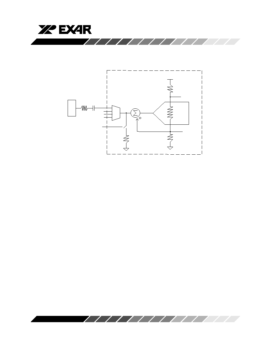
GENERAL DESCRIPTION
The XRD98L23 is a complete linear CIS or CCD sensor
signal processor on a single monolithic chip. The
XRD98L23 includes a high speed 8-bit resolution ADC,
a 6-bit Programmable Gain Amplifier with gain adjust-
ment of 1 to 10, and a typical 8-bit programmable input
referred offset calibration range of 480mV.
In the CCD configuration the input signal is AC coupled
with an external capacitor. An internal clamp sets the
black level. In the CIS configuration, the clamp switch
can be disabled and the CIS output signal is DC
coupled from the CIS sensor to the XRD98L23. The
CIS signal is level shifted to VRB in order to use the full
range of the ADC. In the CIS configuration the input can
also be AC coupled similar to the CCD configuration.
This enables CIS signals with large black levels to be
internally clamped to a DC reference equal to the black
level. The DC reference is internally subtracted from
the input signal.
The CIS configuration can also be used in other
applications that do not require CDS function, such as
low cost data acquisition.
Rev. 1.00
XRD98L23
2
Rev. 1.00
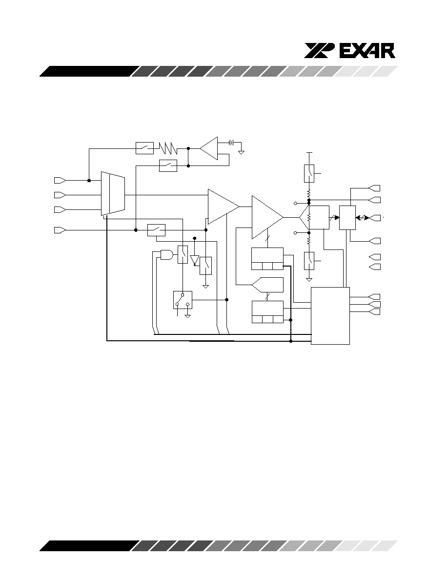
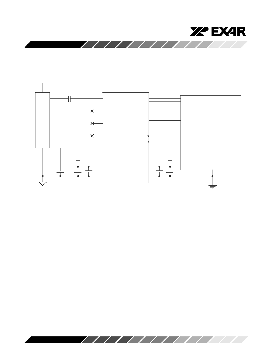
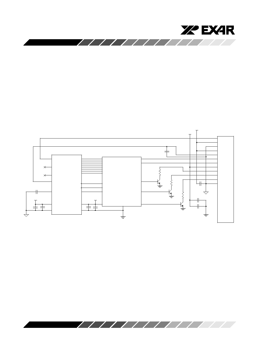
Figure 1. Functional Block Diagram
RED
GRN
BLU
VDCEXT
VREF+
DB7:0
DVDD
DGND
AVDD
AGND
ADCCLK
CLAMP
SYNCH
PGA
TIMING
&
CONTROL LOGIC
AVDD
6-BIT GAIN
REGISTERS
8-BIT
ADC
RL
AGND
DATA
I/O
PORT
BUFFER
VRT
VRB
Triple
S/H
&
3-1
MUX
8-BIT DAC
8
8
8-BIT OFFSET
REGISTERS
6
8
+
_
AGND
V
DCREF
DC/AC
INT/EXT_V DCREF
CIS/CCD
G<5:0>
O<7:0>
R
G
B
R
G
B
CLP
C
L
A
M
P
Power
Down
Power
Down
VRT
CCD
CIS
VBG
CIS REF Circuit
CIS REF Circuit
DC Reference
XRD98L23
3
Rev. 1.00
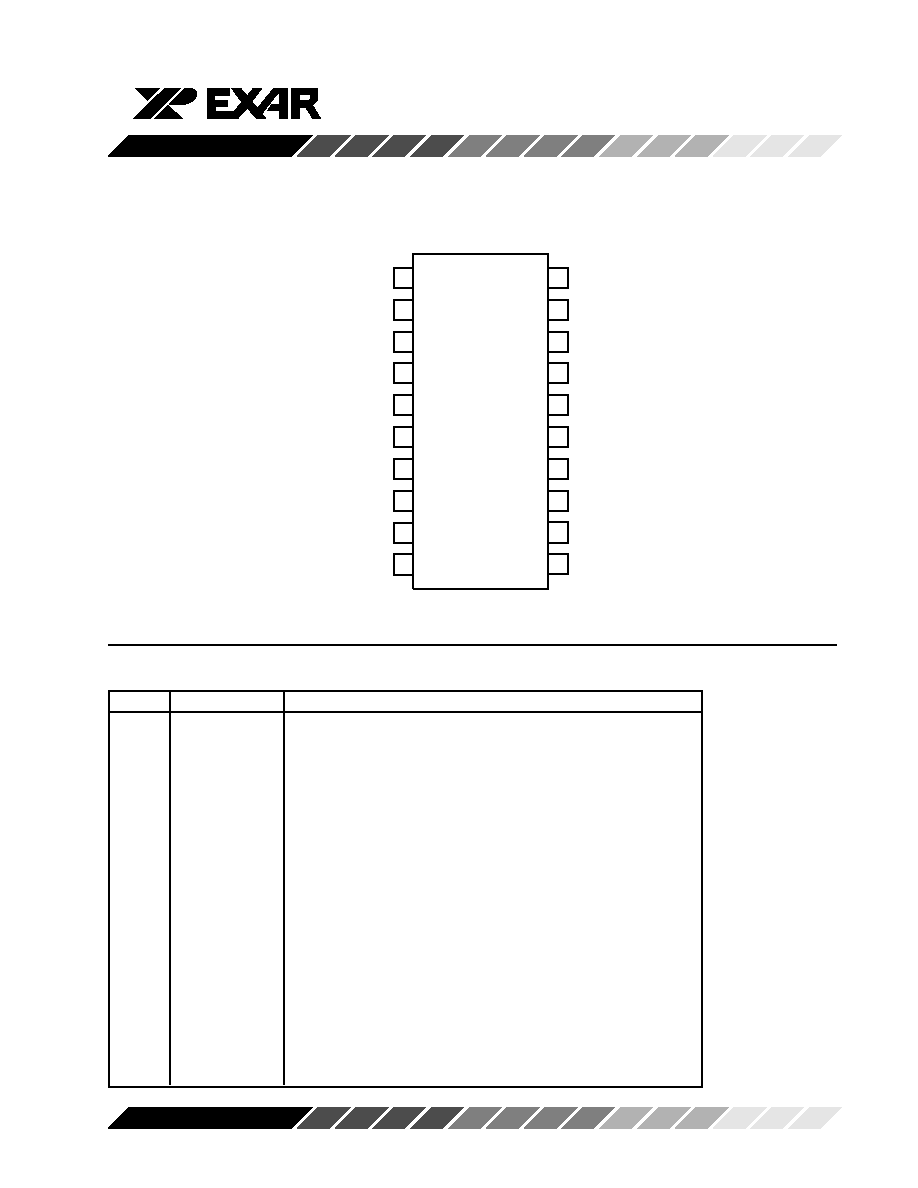
1
2
3
4
5
6
7
8
9
10
AVDD
VREF+
XRD98L23ACD
20
19
18
17
16
15
14
13
12
RED
GRN
BLU
VDCEXT
AGND
DVDD
DB0
DB1
DB2
DB4
DGND
ADCCLK
DB3
11
DB5/SCLK
DB6/SDATA
DB7/LD
CLAMP
SYNCH
20-Lead SOIC
PIN DESCRIPTION
Pin #
Symbol
Description
1
DVDD
Digital VDD (for Output Drivers)
2
DB0
Data Output Bit 0
3
DB1
Data Output Bit 1
4
DB2
Data Output Bit 2
5
DB3
Data Output Bit 3
6
DB4
Data Output Bit 4
7
DB5/SCLK
Data Output Bit 5 & Data Input SCLK
8
DB6/SDATA
Data Output Bit 6 & Data Input SDATA
9
DB7/LD
Data Output Bit 7 & LD
10
DGND
Digital Ground (for Output Drivers)
11
ADCCLK
A/D Converter Clock
12
CLAMP
Clamp and Video Sample Clock
13
SYNCH
Start of New Line and Serial Data Input Control
14
AGND
Analog Ground
15
VREF+
A/D Positive Reference for Decoupling Cap
16
VDCEXT
External DC Reference
17
BLU
Blue Input
18
GRN
Green Input
19
RED
Red Input
20
AVDD
Analog Power Supply
PIN CONFIGURATION
XRD98L23
4
Rev. 1.00
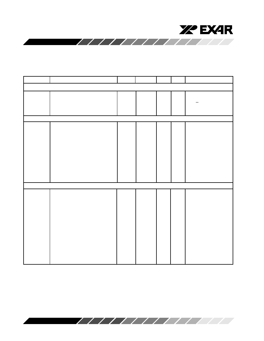
ELECTRICAL CHARACTERISTICS
Test Conditions: AV
DD
=DV
DD
=3.3V, ADCCLK=10MHz, 50% Duty Cycle, T
A
=25∞C unless otherwise specified.
Symbol
Parameter
Min.
Typ.
Max.
Unit
Conditions
Power Supplies
AV
DD
Analog Power Supply
3.0
3.3
3.6
V
DV
DD
Digital I/O Power Supply
3.0
3.3
3.6
V
DV
DD
< AV
DD
I
DD
Supply Current (total)
25
60
mA
V
DD
=3.0V
IDD
PD
Power Down Power Supply Current
50
µ
A
V
DD
=3.0V
ADC Specifications
RES
Resolution
8
Bits
F
s
Maximum Sampling Rate
12
MSPS
DNL
Differential Non-Linearity
±0.5
LSB
INL
Integral Non-Linearity
±1.0
LSB
MON
Monotonicity
Yes
V
RT
Top Reference Voltage
2.1
2.2
2.6
V
V
RB
Bottom Reference Voltage
AV
DD
/10
V
DV
REF
Differential Reference Voltage
0.18
0.67AV
DD
V
(V
RT
- V
RB
)
R
L
Ladder Resistance
300
600
780
PGA & Offset DAC Specifications
PGARES
PGA Resolution
6
Bits
PGAG
MIN
Minimum Gain
0.950
1.0
1.35
V/V
PGAG
MAX
Maximum Gain
9.5
10.0
10.50
V/V
PGAGD
Gain Adjustment Step Size
0.14
V/V
V
BLACK
Black Level Input Adjust Range
-60
+300
mV
DC Configuration
DACRES
Offset DAC Resolution
8
Bits
OFF
MIN
Minimum Offset Adjustment
-180
-120
-80
mV
Mode 111, D5=0 (Note 1)
OFF
MAX
Maximum Offset Adjustment
+200
+360
+400
mV
Mode 111, D5=0
OFF
MIN
Minimum Offset Adjustment
-350
-240
-100
mV
Mode 111, D5=1 (Note 1)
OFF
MAX
Maximum Offset Adjustment
+100
+240
+350
mV
Mode 111, D5=1
OFF
Offset Adjustment Step Size
1.88
mV
Note 1:
The additional ±60 mV of adjustment with respect to the black level input range is needed to compensate
for any additional offset introduced by the XRD98L23 Buffer/PGA internally.
XRD98L23
5
Rev. 1.00
ELECTRICAL CHARACTERISTICS (CONT'D)
Test Conditions: AV
DD
=DV
DD
=3.3V, ADCCLK=10MHz, 50% Duty Cycle, T
A
=25∞C unless otherwise specified.
Symbol
Parameter
Min.
Typ.
Max.
Unit
Conditions
Buffer Specifications
I
IL
Input Leakage Current
100
nA
CIN
Input Capacitance
10
pF
VIN
PP
AC Input Voltage Range
0
AV
DD
-1.4
V
CIS AC; INT V
DCREF
Config Reg
=> XXX010XX
Gain=1 (Note 1)
AC Input Voltage Range
0
DV
REF
V
CCD AC; INT V
DCREF
Config Reg
=> XXX011XX
Gain=1 (Note 1)
VIN
DC Input Voltage Range
-0.1
AV
DD
-1.4
V
CIS DC; INT V
DCREF
Config Reg
=> XXX000XX
Gain=1 (Note 2)
DC Input Voltage Range
V
DCEXT
-0.1
V
DCEXT
+
V
CIS DC; EXT V
DCREF
DV
REF
Config Reg
=> XXX100XX
Gain=1 (Note 3)
V
DCEXT
+DV
REF
< AV
DD
V
DCEXT
External DC Reference
0.3
AV
DD
/2
V
CIS DC; EXT V
DCREF
Config Reg
=> XXX100XX
VIN
BW
Input Bandwidth (Small Signal)
10
MHz
VIN
CT
Channel to Channel Crosstalk
-60
dB
Internal Clamp Specifications
V
CLAMP
Clamp Voltage
AGND
50
mV
CIS (AC) Config
2.1
V
RT
V
CCD (AC) Config
R
INT
Clamp Switch On Resistance
180
250
R
OFF
Clamp Switch Off Resistance
12
M
Note 1: VIN
PP
is the signal swing before the external capacitor tied to the MUX inputs.
Note 2: The -0.1V minimum is specified in order to accommodate black level signals lower than the external DC
reference (clamp) voltage.
Note 3: The V
DCEXT
-0.1V minimum is specified in order to accommodate black level signals lower than the external DC
reference voltage.

XRD98L23
6
Rev. 1.00
ELECTRICAL CHARACTERISTICS (CONT'D)
Test Conditions: AV
DD
=DV
DD
=3.3V, ADCCLK=10MHz, 50% Duty Cycle, T
A
=25∞C unless otherwise specified.
Symbol
Parameter
Min.
Typ.
Max.
Unit
Conditions
System Specifications (MUX + Buffer + PGA + ADC)
Note 1
SYS
DNL
System DNL
-1.0
±0.5
+2.0
LSB
No missing codes
SYS
LIN
System Linearity
±6.0
LSB
SYS
GE
System Gain Error
-5.0
+5.0
%
IRN
Input Referred Noise
1.5
mV
rms
Gain=1
Input Referred Noise
0.5
mV
rms
Gain=10
System Timing Specifications
tcklw
ADCCLK Low Pulse Width
50
ns
tckhw
ADCCLK High Pulse Width
50
ns
tckpd
ADCCLK Period
100
ns
tsypw
SYNCH Pulse Width
30
ns
trars
Rising ADCCLK to rising
0
SYNCH must rise equal to
SYNCH
or after ADCCLK, See Figure 18
tclpw
CLAMP Pulse Width
30
ns
Note 2
Write Timing Specifications
tsclkw
SCLK Pulse Width
40
ns
tdz
LD Low to SCLK High
20
ns
tds
Input Data Set-up Time
20
ns
tdh
Input Data Hold Time
0
ns
tdl
SCLK High to LD High
50
ns
ADC Digital Output Specifications
tap
Aperture Delay
ns
tdv
Output Data Valid
30
50
ns
tsa
SYNCH to ADCCLK (3ch)
20
ns
3ch Pixel Md
tsa2
SYNCH to ADCCLK (2ch)
20
80
ns
2ch Pixel Md
tlat
Latency
8
cycles
Config 00, 11
tlat
Latency
6
pixels
Config 01, 10
Digital Input Specifications
V
IH
Input High Voltage
AV
DD
-1.5
V
V
IL
Input Low Voltage
0.6
V
I
IH
High Voltage Input Current
5
µ
A
I
IL
Low Voltage Input Current
5
µ
A
C
IN
Input Capacitance
10
pF
Note 1:
System performance is specified for typical digital system timing specifications.
Note 2:
The actual minimum `tclpw' is dependent on the external capacitor value, the CIS output impedance.
During `clamp' operation, sufficient time needs to be allowed for the external capacitor to charge up to the
correct operating level. Refer to the description in Theory of Operation, CIS Config.
XRD98L23
7
Rev. 1.00
ELECTRICAL CHARACTERISTICS (CONT'D)
Test Conditions: AV
DD
=DV
DD
=3.3V, ADCCLK=10MHz, 50% Duty Cycle, T
A
=25∞C unless otherwise specified.
Symbol
Parameter
Min.
Typ.
Max.
Unit
Conditions
Digital Output Specifications
V
OH
Output High Voltage
80
(
%) DVDD
I
L
= 1mA
V
OL
Output Low Voltage
20
(
%) DVDD
I
L
= -1mA
I
Oz
Output High-Z Leakage Current
-10
10
µ
A
C
OUT
Output Capacitance
10
pF
SR
Slew Rate (10% to 90% DV
DD
)
2
15
ns
C
L
= 10pF, DV
DD
= 3.3V

XRD98L23
8
Rev. 1.00
THEORY OF OPERATION
CIS Configuration (Contact Image Sensor)
The XRD98L23 has two configurations for CIS applications. Each configuration is set by the control registers
accessed through the serial port.
Mode 1. DC Coupled
If the CIS does not have leading or trailing black pixels as shown in Figure 2, then DC couple the CIS output to the
XRD98L23 input.
Optically Shielded
Pixels
Valid Pixels
Adjust the offset of the CIS (-60 mV to 300 mV) by setting the internal registers of the XRD98L23 to set the black
pixel value when the LEDs of the CIS are off. When the LEDs are on, use the XRD98L23 Programmable Gain to
maximize the ADCs dynamic range. Figure 3 shows a typical application for a CIS with an offset of -60mV to 300mV.
Figure 2. Typical Output CIS Mode
XRD98L23
9
Rev. 1.00
R
L
VRT
VRB
VDD
RED
XRD98L23
C
I
S
M
U
X
N/C
N/C
N/C
The input is added to VRB before the signal passes
through the ADC. If the CIS output is zero, then the
output of the ADC will be zero code. This enables the
CIS to be referenced to the bottom ladder reference
voltage to use the full range of the ADC.
Some CIS sensors have an output with an offset voltage
of greater than 300mV. If the CIS output is beyond the
offset range of the XRD98L23 (see Offset Control DAC,
Pg. 27) set the internal mode registers to external
reference. An external reference voltage equal to the
value of the CIS offset voltage can be applied to
VDCEXT (Figure 4) in order to meet the dynamic range
of the XRD98L23. Figure 4 is a diagram of the
XRD98L23 in the external reference mode for CIS, DC
coupled applications.
Figure 3. Application with Offset in the Range (-60mv to 300mv)

XRD98L23
10
Rev. 1.00
RL
VRT
VRB
VDD
RED
XRD98L23
DC
REFERENCE
C
I
S
M
U
X
N/C
N/C
VDCEXT
The DC reference voltage applied to VDCEXT does not
have to be accurate. The internal offset DAC voltage is
still used in this mode for fine adjustment. VDCEXT
cannot be used as an input from the CIS. Any signal
applied to VDCEXT will be subtracted from the output
signal of the multiplexer.
Figure 4. Application with Offset Greater Than (-60mv to 300mv)
XRD98L23
11
Rev. 1.00
AGND
DVDD (3V)
VCC (5V - 15V)
AVDD
DGND
AVDD
ASIC
DIGITAL
C
I
S
N/C
N/C
4
K
0
.
1
u
F
0
.
0
1
u
F
0.1uF
0
.
0
1
u
F
0
.
1
u
F
0
.
1
u
F
1
K
XRD98L23
DVDD
1
DB0
2
DB1
3
DB2
4
DB3
5
DB4
6
DB5/SCLK
7
DB6/SDATA
8
DB7/LD
9
DGND
10
ADCCLK
11
CLAMP
12
SYNCH
13
AGND
14
VREF+
15
VDCEXT
16
BLU
17
GRN
18
RED
19
AVDD
20
Figure 5. Typical Application Circuitry CIS DC Coupled Non-Inverted Mode with
VDC External Offset Compensation
XRD98L23
12
Rev. 1.00
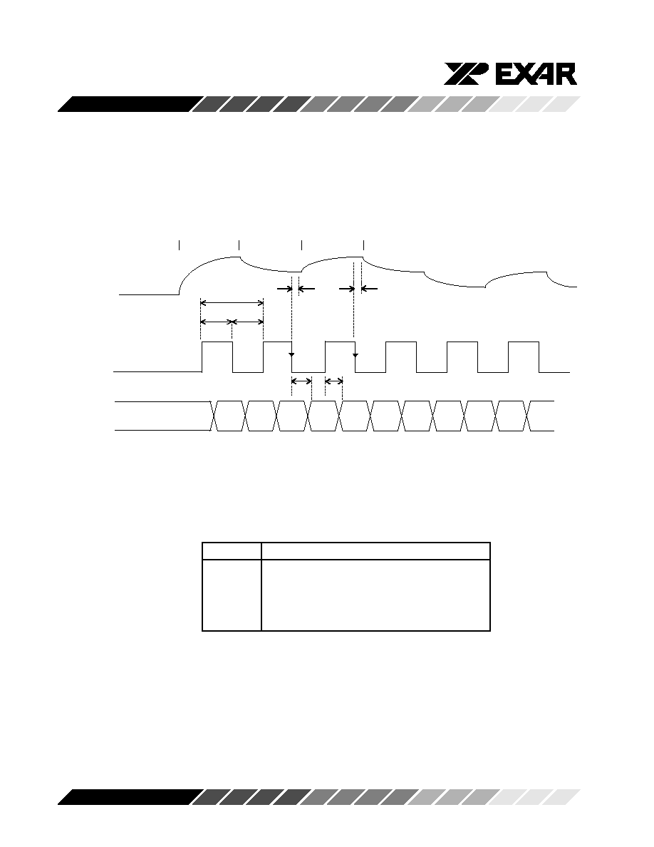
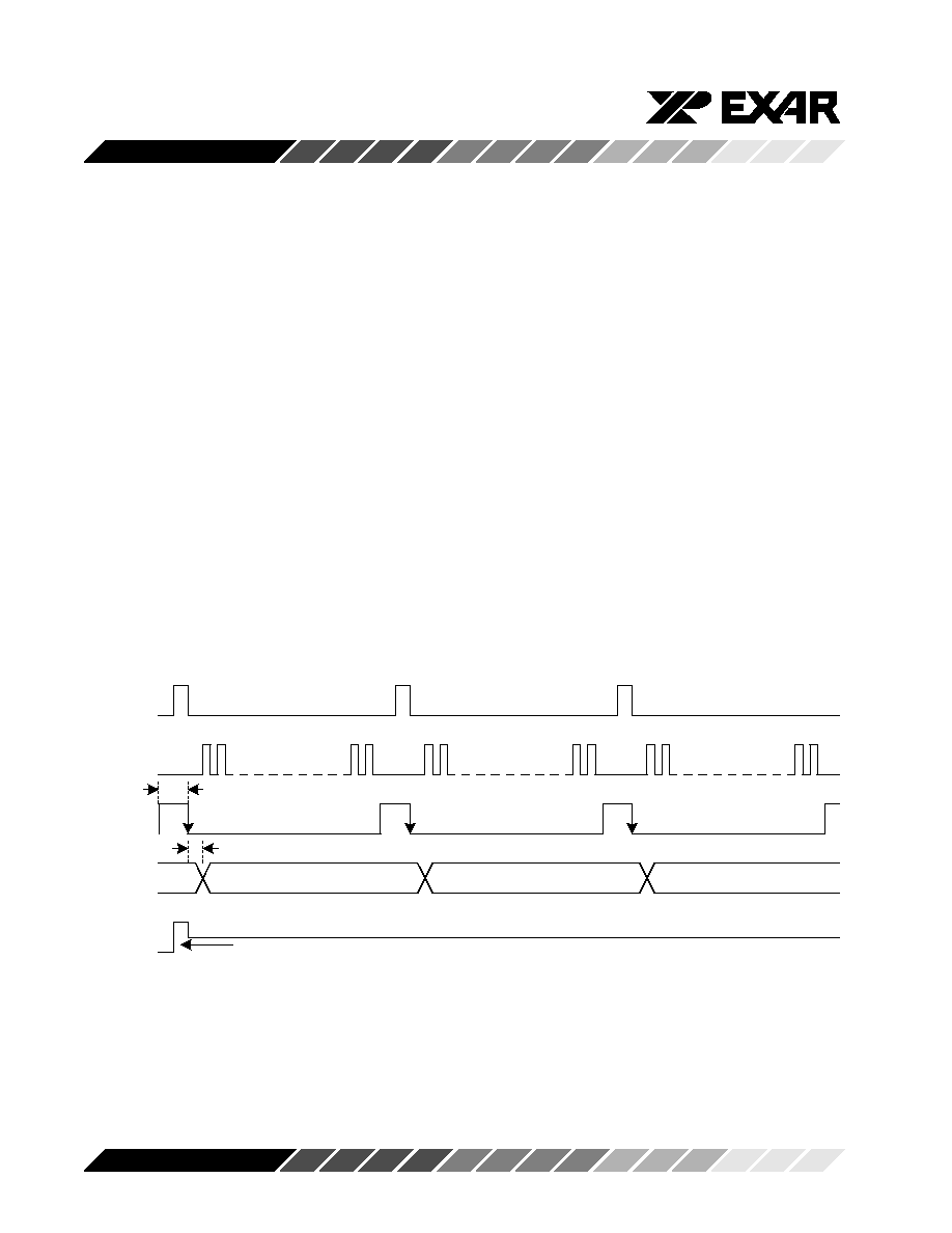
CIS Mode Timing -- DC Coupled
(CLAMP disabled)
ADCCLK
tckhw
tcklw
tckpd
tap
tap
Pixel N-1
Pixel N
tdv
Pixel N+1
CIS
tdv
[7:0]
N-8
N/A
N-7
N/A
N-6
N/A
N-5
N/A
DB
Figure 6. Timing Diagram for Figure 5
ADCCLK
Events
ADC Sample & PGA Start Tracking next Pixel
Data Out
Invalid Data Out
HI
ADC Track PGA Output
LO
ADC Hold/Convert
Table 1.
Mode 2. AC Coupled
If the CIS signal has a black reference for the video
signal, an external capacitor C
EXT
is used. When
CLAMP (clamp) pin is set high an internal switch allows
one side of the external capacitor to be set to ground.
It then is level shifted to correspond to the bottom ladder
reference voltage of the ADC (Figure 7).
XRD98L23
13
Rev. 1.00
R
L
VRT
VRB
VDD
XRD98L23
CLAMP
RINT
RED
M
U
X
C
I
S
REXT CEXT
N/C
N/C
N/C
Therefore, Tc =1/R
INT
C
EXT
If the input to the external capacitor has a source
impedance (R
EXT
), then:
T
c
=1/(R
INT
+R
EXT
)C
EXT
This value corresponds to the black reference of the
image sensor. When the CLAMP pin is set back to low,
the ADC samples the video signal with respect to the
black reference. The typical value for the external
capacitor is 100pF. This value should be adjusted
according to the time constant (Tc) needed in a particu-
lar application. The CLAMP pin has an internal 180 ohm
(from electrical tabels) impedance (R
INT
) which is in
series with the external capacitor (C
EXT
).
Figure 7. CIS AC Coupled Application
XRD98L23
14
Rev. 1.00
DVDD (3V)
AVDD
VCC (5V - 15V)
DGND
AGND
DIGITAL
ASIC
C
I
S
N/C
N/C
N/C
100PF
0
.
1
u
F
0
.
1
u
F
0
.
0
1
u
F
0
.
1
u
F
0
.
0
1
u
F
XRD98L23
DVDD
1
DB0
2
DB1
3
DB2
4
DB3
5
DB4
6
DB5/SCLK
7
DB6/SDATA
8
DB7/LD
9
DGND
10
ADCCLK
11
CLAMP
12
SYNCH
13
AGND
14
VREF+
15
VDCEXT
16
BLU
17
GRN
18
RED
19
AVDD
20
Figure 8. Typical Application Circuitry CIS AC Coupled Non-Inverted
XRD98L23
15
Rev. 1.00
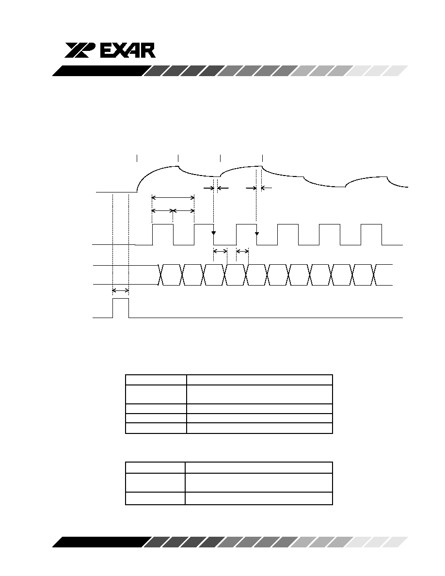
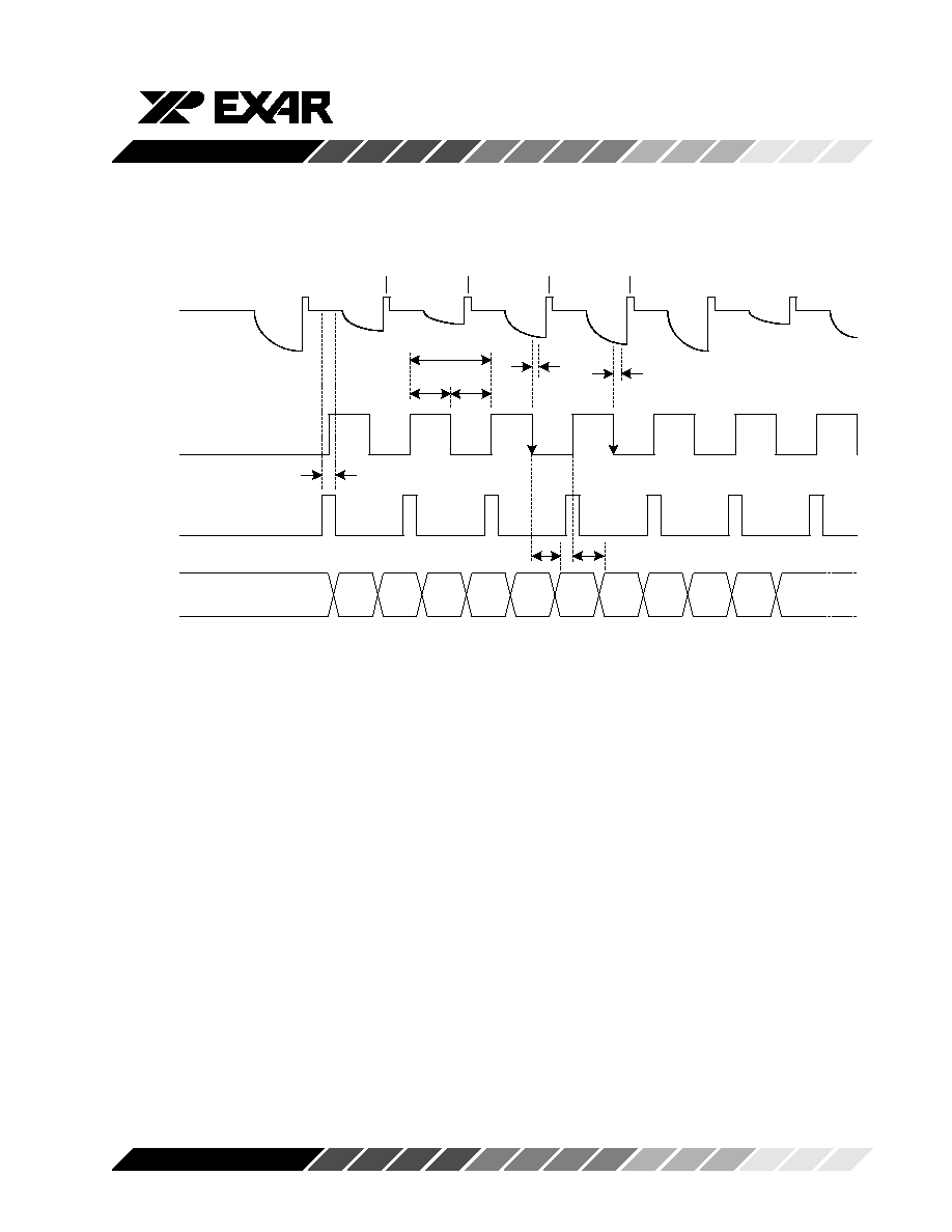
CIS Mode Timing -- AC Coupled
(CLAMP enabled)
ADCCLK
tckhw
tcklw
tckpd
tap
tap
Pixel N-1
Pixel N
tdv
Pixel N+1
CIS
tdv
N-8
N/A
N-7
N/A
N-6
N/A
N-5
N/A
CLAMP
tclpw
DB [7.0]
Figure 9. Timing Diagram for Figure 8
ADCCLK
Events
ADC Sample & PGA Start Track of next Pixel
Data Out
Invalid Data Out
HI
ADC Track PGA Output
LO
ADC Hold/Convert
Table 2.
CLAMP
Events
HI
PGA Tracks V
CLAMP
& C
EXT
is Charged to
V
BLACK
- V
CLAMP
, which is equal to V
BLACK
LO
PGA Tracks VIN
PP
Table 3.
XRD98L23
16
Rev. 1.00
Internal CIS Reference Circuit (DB 4 = 1)
The XRD98L23 has an internal register reserved for
interfacing to the Canon CIS model number CVA-
60216K. When this register is selected, the VDCEXT
(Pin 16) becomes an output voltage of 1.24 volts. This
voltage can be directly connected to the VREF (Pin 5)
of the Canon sensor. This reduces the amount of
components needed for biasing the Canon CIS sensor
(the external diodes and resistors typically used in this
application have been included inside the XRD98L23
Figure 10. Typical Application Circuitry Internal CIS Reference Circuit Mode
CANON CIS Sensor, Model #CVA=60216K
for this mode of operation). Below is a typical applica-
tion circuit using the XRD98L23 and the Canon CVA-
60216K CIS sensor.
AGN
D
DVDD (3V )
VCC (5V)
AVD
D
DGND
AGN
D
DGND
DGND
DGND
DGND
DVDD (3V - 5V)
ASIC
DIGITAL
N/C
N/C
CANON CIS
SENSOR
0
.
1
u
F
0
.
0
1
u
F
0.1u
F
0
.
0
1
u
F
0
.
1
u
F
XRD98L23
DVDD
1
DB0
2
DB1
3
DB2
4
DB3
5
DB4
6
DB5/SCLK
7
DB6/
SDATA
8
DB7/LD
9
DGND
10
ADCCL
K
11
CLAM
P
12
SYNC
H
13
AGN
D
14
VREF+
15
VDCEX
T
16
BLU
17
GRN
18
RED
19
AVD
D
20
CVA-60216K
VOU
T
1
MOD
E
2
AGN
D
3
VCC
4
VREF
5
SP
6
CLK
7
LED
COM
8
LED BLU
9
LED GRN
10
LED RED
11
FGND
12
1
0
K
1
0
K
1
0
K
47u
F
4
7
u
F
NPN
NPN
NPN
0.01u
F
100u
F

XRD98L23
17
Rev. 1.00
CIS Line-By-Line Rotating Gain and Offset
(Configuration DB1 = 1, DB0 = 1)
Line-by-line rotating gain and offset minimizes the
amount of write cycles per scan. Pre-loaded values of
gain and offset can be loaded for each color before the
first line is scanned. Each gain and offset is cycled
through line-by-line so that the gain and offset do not
have to be loaded in between lines. Below is the typical
application circuit and timing for this configuration.
Figure 11. Typical Application Circuitry Internal CIS Rotating Gain
and Offset Line-By-Line
AVDD
AGND
DGND
VCC (5V - 15V)
DVDD (3V)
ASIC
DIGITAL
C
I
S
N/C
0
.
0
1
u
F
0
.
1
u
F
0.1uF
0
.
1
u
F
XRD98L23
DVDD
1
DB0
2
DB1
3
DB2
4
DB3
5
DB4
6
DB5/SCLK
7
DB6/SDATA
8
DB7/LD
9
DGND
10
ADCCLK
11
CLAMP
12
SYNCH
13
AGND
14
VREF+
15
VDCEXT
16
BLU
17
GRN
18
RED
19
AVDD
20
0
.
0
1
u
F
XRD98L23
18
Rev. 1.00
CCD Configuration (Charge Coupled Device)
Mode 1. AC Coupled
In the CCD configuration of operation, an external
capacitor needs to be chosen according to the equa-
tions below. The typical value for the external capacitor
is 100pF. This value should be adjusted according to
the time constant (Tc) needed in a particular applica-
tion. The CLAMP pin has an internal 180 ohm imped-
ance (R
INT
) which is in series with the external capacitor
(C
EXT
).
Therefore, Tc =1/R
INT
C
EXT
If the input to the external capacitor has a load imped-
ance (R
EXT
), then
T
c
=1/(R
INT
+R
EXT
)C
EXT
When CLAMP (clamp) pin is set high an internal switch
allows one side of the external capacitor to be set to
VRT (Figure 13). This value corresponds to the black
reference of the CCD. When the CLAMP pin is set back
to low, the ADC samples the video signal with respect
to the black reference. The difference between the
black reference and the video signal is the actual pixel
value of the video content. Since this value is refer-
enced to the top ladder reference voltage of the ADC a
zero input signal would yield a full scale output code.
Therefore, the output of the conversion is inverted
(internally) to correspond to zero scale output code.
Figure 12. Timing Diagram for Figure 11
CIS Rotating Gain and Offset
Line-By-Line (Md 11)
ADCCLK
CIS
SYNCH
GAIN/
OFFSET
LD
Red Pixel Line Scan
Grn Pixel Line Scan
Blu Pixel Line Scan
Red Gain/Offset Cycle
Grn Gain/Offset Cycle
Blu Gain/Offset Cycle
Reset Internal Mux Color to Red Channel (LD = 110YYYYYY11)
tsa
tsypw
Note: Y = Previous State
Tri-State (SYNCH = LO)

XRD98L23
19
Rev. 1.00
Area or Linear CCD Applications
Figure 13, is a block diagram for applications with Area
or Linear CCDs (The timing for Area CCDs and B/W
CCDs is the same). For Area or Linear CCD applica-
tions, a global offset is loaded into the serial port at the
beginning of a line. The gain is set to adjust for the
highest color intensity of the CCD output. Once the
pixel values have been sampled, the gain and offset are
adjusted at the beginning of the next line. For example,
if there is a line-to-line variation between the black
reference pixels, the offset is adjusted. The gain is
always adjusted for the highest color intensity.
Figure 13. CCD AC Coupled Application
RL
VRT
VRB
VDD
RED
XRD98L23
CLAMP
M
U
X
AREA
or
LINEAR
CCD
N/C
N/C
N/C

XRD98L23
20
Rev. 1.00
Figure 14. Typical Application Circuitry for a Single
Channel B/W CCD AC Coupled Inverted Mode
DVDD (3V)
AVDD
VCC (5V - 15V)
DGND
AGND
DIGITAL
ASIC
C
C
D
N/C
N/C
N/C
100PF
0
.
1
u
F
0
.
1
u
F
0
.
0
1
u
F
0
.
1
u
F
0
.
0
1
u
F
XRD98L23
DVDD
1
DB0
2
DB1
3
DB2
4
DB3
5
DB4
6
DB5/SCLK
7
DB6/SDATA
8
DB7/LD
9
DGND
10
ADCCLK
11
CLAMP
12
SYNCH
13
AGND
14
VREF+
15
VDCEXT
16
BLU
17
GRN
18
RED
19
AVDD
20
XRD98L23
21
Rev. 1.00
tdv
tdv
AREA, LINEAR or B/W CCD -- AC Coupled
(CLAMP Enabled)
Pixel N-1
Pixel N
Pixel N+1
CCD
Channel N
ADCCLK
tckpd
tap
tap
tckhw
tcklw
CLAMP
tclpw
N-8
N/A
N-7
N/A
N-6
N.A
[7:0]
DB
Figure 15. Timing Diagram for Figure 14
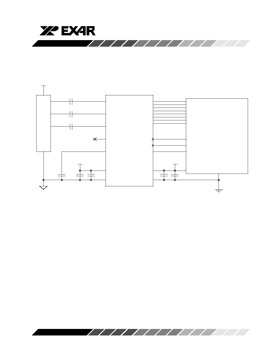
Triple Channel CCD Application
Figure 16, is a block diagram for pixel-by-pixel applica-
tions with triple channel CCDs. During the optically
shielded section of a pixel, CLAMP must go high to
store the black reference on each capacitor to the input.
The gain and offset is automatically rotated to adjust for
each channel input. The data is available on the output
bus on the falling edge of ADCCLK.
XRD98L23
22
Rev. 1.00
RL
VRT
VRB
VDD
RED/GRN/BLU
XRD98L23
CLAMP
C
C
D
M
U
X
N/C
Figure 16. CCD AC Coupled Application
XRD98L23
23
Rev. 1.00
AVDD
VCC (5V - 15V)
DGND
AGND
DIGITAL
ASIC
C
C
D
N/C
100PF
0
.
1
u
F
0
.
1
u
F
0
.
0
1
u
F
0
.
1
u
F
0
.
0
1
u
F
100PF
100PF
XRD98L23
DVDD
1
DB0
2
DB1
3
DB2
4
DB3
5
DB4
6
DB5/SCLK
7
DB6/SDATA
8
DB7/LD
9
DGND
10
ADCCLK
11
CLAM
P
12
SYNCH
13
AGND
14
VREF+
15
VDCEXT
16
BLU
17
GRN
18
RED
19
AVDD
20
DVDD (3V)
Figure 17. Typical Application Circuitry Triple Channel CCD
AC Coupled Inverted Mode
XRD98L23
24
Rev. 1.00
(CLAMP Enabled)
BLU
GRN
RED
ADCCLK
CLAMP
DATA
PIXEL-BY-PIXEL 3 CHANNEL CCD -- AC Coupled
tdv
RED (N-6)
N+1 Pixel
CONVERT
RED (N)
CONVERT
GRN (N)
CONVERT
BLU (N)
TRACK
RED (N)
TRACK
GRN (N)
TRACK
RED (N+1)
TRACK
BLU (N)
CONVERT
RED (N+1)
tdv
tdv
tdv
tdv
N/A
GRN (N-6)
N/A
BLU (N-6)
N/A
CLAMP
tsa
SYNCH
tsypw
tclp=10ns
tap
tclp=10ns
N+1 Pixel
N+1 Pixel
N Pixel
N Pixel
N Pixel
Simultaneous
Sample
trars
ADCCLK
Events
3rd
Simultaneous RED/GRN/BLU Sample Every 3rd CLK.
Convert RED, S/H GRN, S/H BLU.
All
Data Out
Non-valid Data Out
HI
ADC Track PGA Output
LO
ADC Hold/Convert
CLAMP
Events
HI
Internal Clamp Enabled
LO
Internal RED/GRN/BLU Tracking Enabled
SYNCH
Events
HI
Reset Internal Mux to Red, Output Bus is Tri-stated
LO
Increment Mux Color on Falling Edge of ADCCLK
Table 4.
Figure 18. Timing Diagram for Figure 17
XRD98L23
25
Rev. 1.00
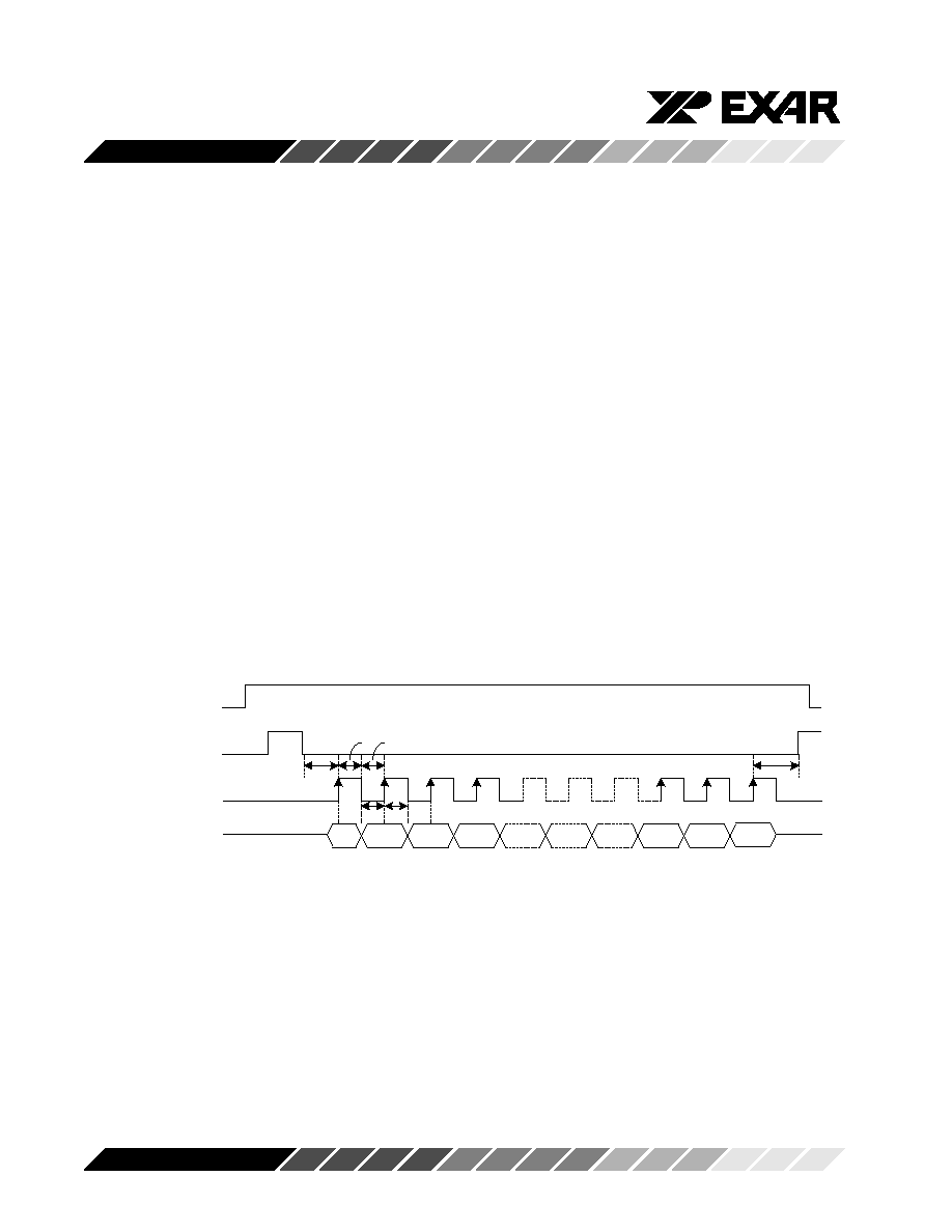
Figure 19. Timing Diagram for 2-channel
GRN
RED
ADCCLK
DATA
PIXEL-BY-PIXEL 2-CHANNEL CCD
tdv
RED(N_6)
N+1 Pixel
CONVERT
RED (N)
CONVERT
GRN (N)
CONVERT
TRACK
RED (N)
TRACK
GRN (N)
TRACK
GRN (N+1)
TRACK
RED (NH)
CONVERT
GRN (N+1)
tdv
tdv
tdv
tdv
N/A
GRN(N-6)
N/A
RED(N-5)
N/A
CLAMP
tsa2
SYNCH
tsypw
tap
N+1 Pixel
N Pixel
N Pixel
Simultaneous
Sample
trars
RED (NH)
tsypw
XRD98L23
26
Rev. 1.00
T/H
T/H
T/H
From CCD RED
Channel
From CCD
GRN Channel
From CCD BLU
Channel
8-Bit ADC
S1 S2 S3
S4
S5
S6
S7
S8
S9
ADCCLK
CLAMP
S4 and S5 open
at this falling
edge
S6 opens, S7
closes at this
rising edge
S7 opens, S8
closes at this
rising edge
S8 Opens, S4,
S5 and S6
close at this
rising edge
Track
GRN
Track
BLU
Track
RED
Track
RED
Convert
RED
Convert
RED
Convert
GRN
Convert
BLU
CCD
Waveform
S8 Opens, S4,
S5 and S6
close at this
rising edge
S9 closes at rising edge and opens
at falling edge of ADCCLK
S1, S2 and S3 close when
CLAMP is high and open
when CLAMP is low
-
+
PGA
C EXTR
C EXTG
C EXTB
VCDS = PGAG * [V
RT
- (V
RT
- V
PIX
)]
= PGAG * V
PIX
XRD98L23
V
RT -
V
RT
V
RT
V
PIX
V
PIX
V
PIX
V
BLK
V
BLK
-
Figure 20. CDS Timing (Triple Channel)
Mode: 110 00001110
XRD98L23
27
Rev. 1.00
Mode 2. DC Coupled
Typical CCDs have outputs with black references.
Therefore, DC Coupled is not recommended for CCD
applications.
Offset Control DAC
The offset DAC is controlled by 8-bits. The offset range
is 480 mV ranging from -120 mV to +300 mV (when DB5
is set to 0) and -240 mV to +240 mV (when DB5 is set
to 1). Therefore, the resolution of the 8-bit offset DAC
is 1.88 mV. However, the XRD98L23 has +/- 60 mV
reserved for internal offsets. Therefore, the effective
range for adjusting for CIS offsets or black reference is
300 mV. The offset adjustment is used primarily to
correct for the difference between the black level of the
image sensor and the bottom ladder reference voltage
(VRB) of the ADC. By adjusting the black level to
correspond to VRB, the entire range of the ADC can be
used.
If the offset of the CIS output is greater than 300 mV an
external reference can be applied to VDCEXT. The
external reference can be used to adjust for large
offsets only when the internal mode is configured
through the serial port.
Since the offset DAC adjustment is done before the
gain stage, it is gain-dependent. For example, if the
gain needs to be changed between lines (red to blue,
etc.), the offset is calibrated before the signal passes
through the PGA.
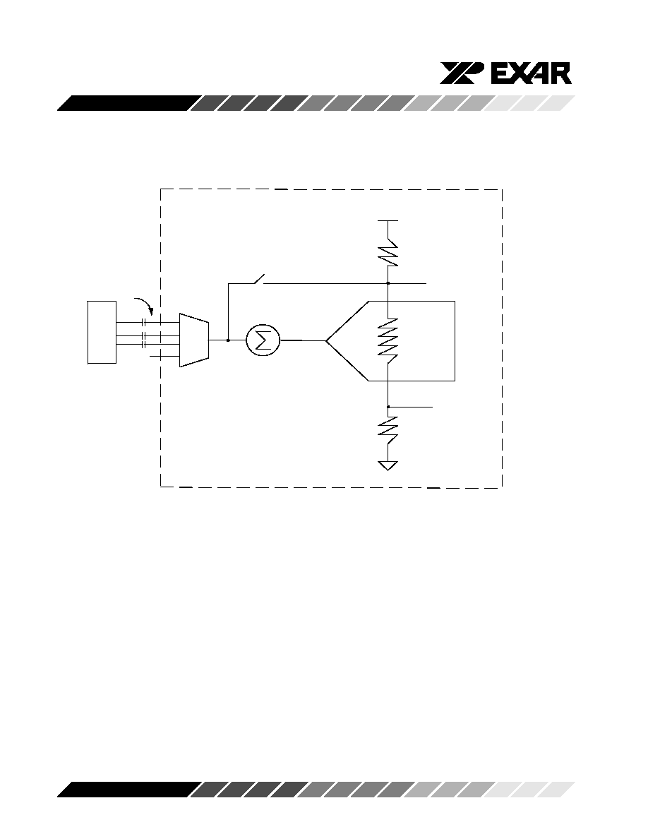
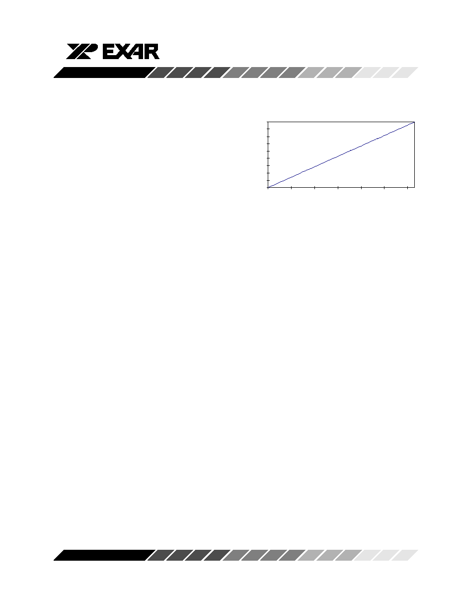
PGA (Programmable Gain Amplifier) DAC
The gain of the input waveform is controlled by a 6-Bit
PGA. The PGA is used along with the offset DAC for
the purpose of using the entire range of the ADC. The
PGA has a linear gain from 1 to 10. Figure 20, is a plot
of the transfer curve for the PGA gain.
PGA GAIN TRANSFER CURVE
GAIN 1 - 10
1
2
3
4
5
6
7
8
9
10
0
10
20
30
40
50
60
CODE
GAIN
Figure 21. Transfer Curve for the 6-Bit PGA
After the signal is level shifted to correspond with the
bottom ladder reference voltage, the system can be
calibrated such that a white video pixel can represent
the top ladder reference voltage to the ADC. This allows
for a full scale conversion maximizing the resolution of
the ADC.
Analog to Digital Converter
The ADC is an 8-bit, 10 MSPS analog-to-digital con-
verter for high speed and high accuracy. The ADC uses
a subranging architecture to maintain low power con-
sumption at high conversion rates. The output of the
ADC is on 8-bit databus. ADCCLK samples the input
on its falling edge. After the input is sampled, the data
is latched to the output drivers. On the rising edge of
the ADCCLK, invalid data is latched to the output
drivers. There is an 8 clock cycle latency (Config 00,
11) or 6 pixel count latency (Config 01, 10) for the
analog-to-digital converter.
The V
RT
and V
RB
reference voltages for the ADC are
generated internally, unless the external V
RT
is se-
lected. In the external V
RT
mode, the V
RT
voltage is set
through the VREF+ pin. This allows the user to select
the dynamic range of the ADC.
XRD98L23
28
Rev. 1.00
Serial Load Control Registers
The serial load registers are controlled by a three wire
serial interface through the bi-directional parallel port to
reduce the pin count of this device. When SYNCH is set
to high, the output bus is tri-stated and the serial
interface is activated. DB7/LD, DB5/SCLK and DB6/
SDATA are the three input signals that control this
process. The DB7/LD signal is set low to initiate the
loading of the internal registers.
There are internal registers that are accessed via an 11-
bit data string. Data is shifted in on the rising edge of
SCLK and loaded to the registers on the rising edge of
LD. The data on pin DB6/SDATA is latched automati-
cally after eleven DB5/SCLKs have been counted. If
eleven clocks are not present on DB5/SCLK before the
DB7/LD signal returns high, no data will be loaded into
the internal registers. If more than 11 clocks are
present on DB5/SCLK, the additional clocks will be
ignored. The data corresponding to the first eleven
DB5/SCLKs will be loaded only.
The first three MSBs choose which internal register will
be selected. The remaining 8 LSBs contain the data
needed for programming the internal register for a
particular configuration.
Power-Up State of the Internal Registers
The control register settings upon initial power-up are
for CIS, DC Coupled configuration (V
RT
is set to internal,
Input DC Reference=AGND and the input to the ADC is
selected through the RED channel). Gain is unity and
Offset is set to zero. The test modes are disabled in the
power-up state.
DB6/SDATA
DB5/SCLK
SYNCH
S2
S1
S0
D7
D2
D1
D0
DB7/LD
tdl
tdz
tsclkw
tds tdh
Figure 22. Write Timing
XRD98L23
29
Rev. 1.00
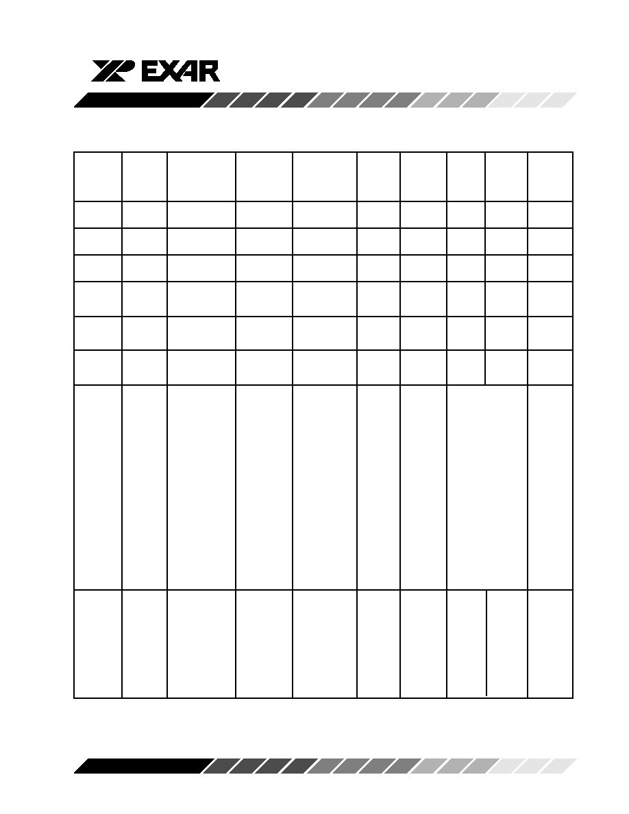
Note :
These are the control register settings upon initial power-up. The previous register settings are retained
following
a logic power-down initiated by the power down bit except the signal configuration. When
de-selecting the power down bit (D7 = 0, Normal), the signal configuration (D5 and D0) has to be
reprogrammed.
Function
(Register
S2/S1/S0)
D7
D6
D5
D4
D3
D2
D1
D0
Power-up
State
(Note 1)
Red Gain
G5
G4
G3
G2
G1
G0
X
X
000000XX
(000)
(MSB)
(LSB)
Red Offset
O7
O6
O5
O4
O3
O2
O1
O0
01000000
(001)
(MSB)
(LSB)
Grn Gain
G5
G4
G3
G2
G1
G0
X
X
000000XX
(010)
(MSB)
(LSB)
Grn Offset
(011)
O7
O6
O5
O4
O3
O2
O1
O0
01000000
(MSB)
(LSB)
Blu Gain
(100)
G5
G4
G3
G2
G1
G0
X
X
000000XX
(MSB)
(LSB)
Blu Offset
(101)
O7
O6
O5
O4
O3
O2
O1
O0
01000000
(MSB)
(LSB)
Mode
POWER
DIGITAL
V
RT
INPUT DC
DC/AC
SIGNAL
SIGNAL
00000000
(110)
DOWN
RESET
REFERENCE
POLARITY
CONFIGURATION
(V
DCREF
)
0: NORMAL
0: NO RESET
0: INTERNAL
0: INTERNAL
0: DC
0: Non-
00: Single-Channel
(V
DCREF
=AGND)
Inverted
RED input/gain/offset
1:
1:RESET
1: EXTERNAL
1: EXTERNAL
1: AC
(CIS)
POWER
(REGISTERS
(V
DCREF
=V
DCEXT
)
1: Inverted
01: Single-Channel
DOWN
ARE RESET TO
(CCD/CIS)
RED input
POWER-UP
RED/GRN/BLU
STATES)
gain/offset cycle
pixel-by-pixel or dual
channel RED/GRN
10: Triple-Channel
RED/GRN/BLU
input/gain/offset cycle
pixel-by-pixel
11: Triple-Channel
RED/GRN/BLU
input/gain/offset cycle
line-by-line
Mode
OUTPUT
OUTPUT
OFFSET
INTERNAL CIS
TEST4
TEST3
TEST2
TEST1
00000000
&Test
BUS
DISABLE
DAC
REFERENCE
(111)
CONTROL
RANGE
CIRCUIT
Must be
0:OUTPUTS
0:-120mV to
0:NORMAL
0: TEST4
0: TEST3
0: TEST2
0:NORMAL
Programmed
ENABLED
+360mV
DISABLED
DISABLED
DISABLED
to 1
1:OUTPUTS
1:-280mV to
1:REFERENCE
1: OUTPUT
1: OUTPUT
1: INPUT
1: TEST1
DISABLED
+240mV
CIRCUIT
OF BUFFER
OF PGA
OF ADC
ENABLED
ENABLED
TIED TO
TIED TO
TIED TO
BLU
VDCEXT
GRN
Control Registers
XRD98L23
30
Rev. 1.00
XRD98L23
31
Rev. 1.00
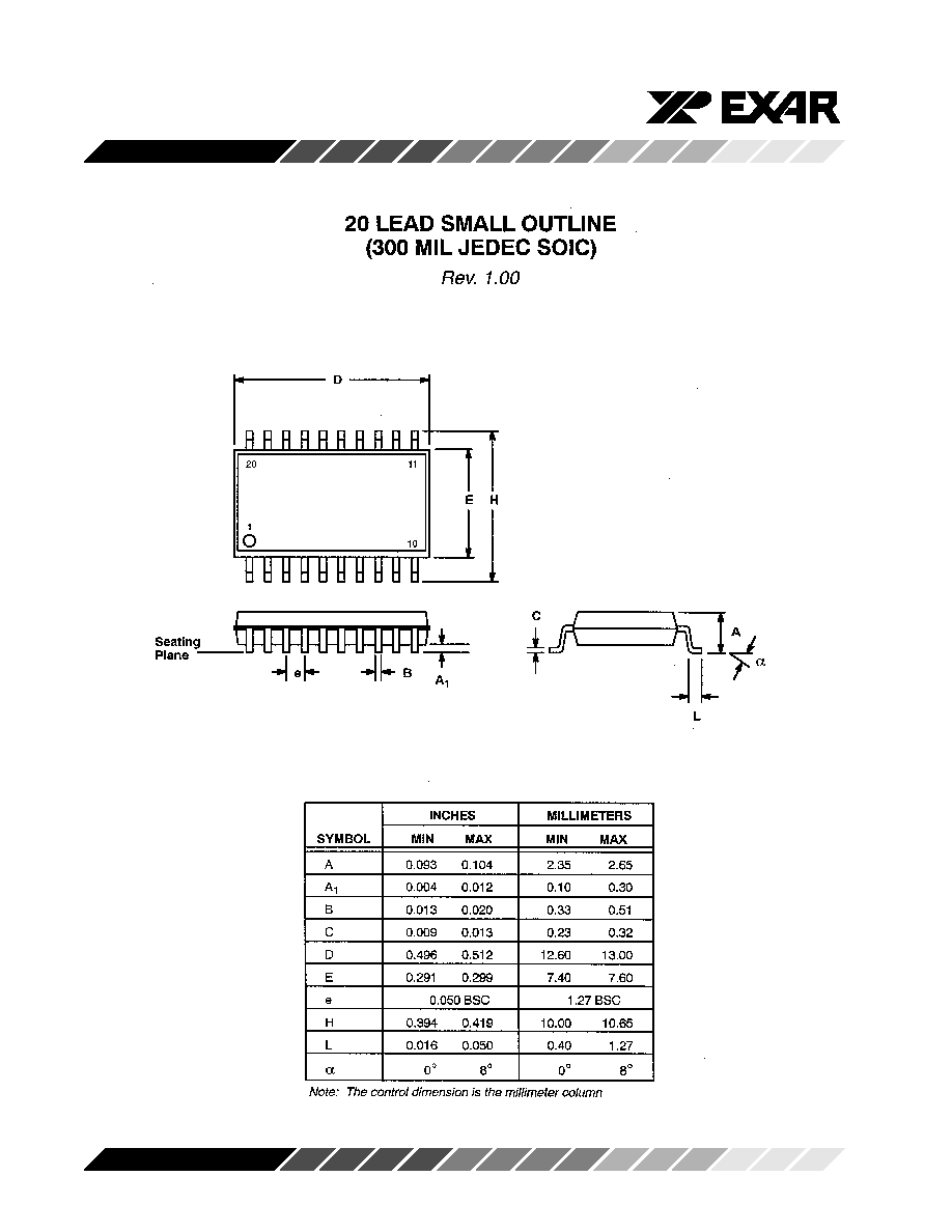
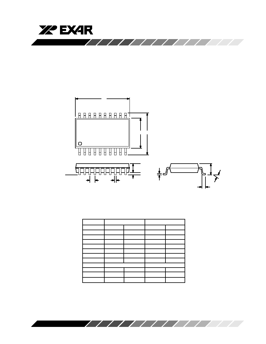
20 LEAD SHRINK SMALL OUTLINE PACKAGE
(5.3 mm SSOP)
Rev. 2.00
20
11
10
e
D
E
H
B
A
L
C
A
1
Seating
Plane
A
2
1
INCHES
MILLIMETERS
SYMBOL
MIN
MAX
MIN
MAX
A
0.067
0.079
1.70
2.00
A1
0.002
0.006
0.05
0.15
A2
0.065
0.073
1.65
1.85
B
0.009
0.015
0.22
0.38
C
0.004
0.010
0.09
0.25
D
0.272
0.296
6.90
7.50
E
0.197
0.221
5.00
5.60
e
0.0256 BSC
0.65 BSC
H
0.292
0.323
7.40
8.20
L
0.022
0.037
0.55
0.95
0∞
8∞
0∞
8∞
Note: The control dimension is the inch column

XRD98L23
32
Rev. 1.00
NOTICE
EXAR Corporation reserves the right to make changes to the products contained in this publication in order to
improve design, performance or reliability. EXAR Corporation assumes no responsibility for the use of any
circuits described herein, conveys no license under any patent or other right, and makes no representation that
the circuits are free of patent infringement. Charts and schedules contained here in are only for illustration
purposes and may vary depending upon a user's specific application. While the information in this publication
has been carefully checked; no responsibility, however, is assumed for in accuracies.
EXAR Corporation does not recommend the use of any of its products in life support applications where the
failure or malfunction of the product can reasonably be expected to cause failure of the life support system or to
significantly affect its safety or effectiveness. Products are not authorized for use in such applications unless
EXAR Corporation receives, in writing, assurances to its satisfaction that: (a) the risk of injury or damage has
been minimized; (b) the user assumes all such risks; (c) potential liability of EXAR Corporation is adequately
protected under the circumstances.
Copyright 2000 EXAR Corporation
Datasheet November 2002
Reproduction, in part or whole, without the prior written consent of EXAR Corporation is prohibited.