EXAR Corporation, 48720 Kato Road, Fremont, CA 94538
∑
(510) 668-7000
∑
FAX (510) 668-7017
∑
www.exar.com
XRD98L62
CCD Image Digitizers with
CDS, PGA and 12-Bit A/D
July 2000-4
FEATURES
∑
12-bit Resolution ADC
∑
30MHz Sampling Rate
∑
10-bit Programmable Gain: 0dB to 36dB PGA
∑
Digitally Controlled Offset-Calibration with Pixel
Averager and Hot Pixel Clipper
∑
DNS Filter Removes Black Level Digital Noise
∑
Widest Black Level Calibration Range at
Maximum Gain
∑
1ns/step Programmable Aperture Delay on SPIX,
SBLK and ADCLK
∑
Manual Control of Offset DAC via Serial Port for
use with High-speed Scanners
∑
Single 2.7V to 3.6V Power Supply
∑
Optimize Power with External Resistor to 180mW
∑
View Finder Mode, 6-bit Resolution, 25%
Less Power
∑
Low Power for Battery Operation
APPLICATIONS
∑
Mega pixel Digital Still Cameras
∑
Digital Camcorders
∑
3 CCD Professional/Broadcast Camera
∑
Line Scan Cameras
∑
PC Video Cameras
∑
CCTV/Security Cameras
∑
Industrial/Medical Cameras
∑
2D Bar Code Readers
∑
High Speed Scanners
∑
Digital Copiers
GENERAL DESCRIPTION
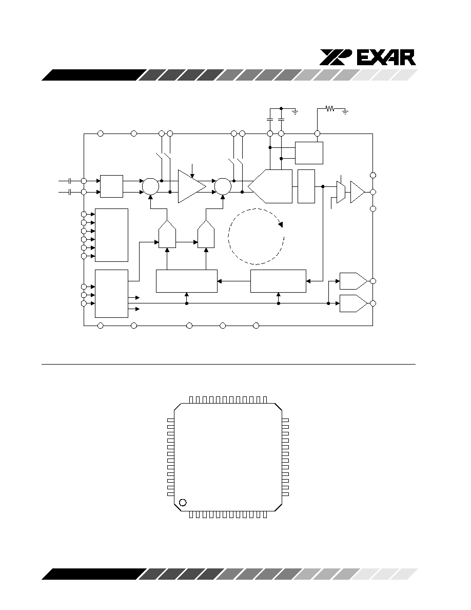
The XRD98L62 is a complete, low power CCD Image
Digitizer for digital motion and still cameras. The
product includes a high bandwidth differential Corre-
lated Double Sampler (CDS), 10-bit digitally Program-
mable Gain Amplifier (PGA), 12-bit Analog-to-Digital
Converter (ADC) and improved digitally controlled
black level auto-calibration circuitry with program-
mable pixel averager, hot pixel clipper, and a DNS
filter.
Two 8-bit serial controlled digital-to-analog converter
(DACs) are provided to control external analog signals
(Iris, Focus, Flash, etc.)
The Correlated Double Sampler (CDS) subtracts the
CCD output signal black level from the video level.
Common mode signal and power supply noise are
rejected by the differential CDS input stage.
The PGA is digitally controlled with 10-bit resolution on
a linear dB scale, resulting in a gain range of 0dB to
36dB with 0.047dB per LSB of the gain code.
The auto calibration circuit compensates for any inter-
nal offset of the XRD98L62 as well as black level offset
from the CCD.
The PGA and black level auto-calibration are con-
trolled through a simple 3-wire serial interface. The
timing circuitry is designed to enable users to select a
wide variety of available CCD and image sensors for
their applications. Readback of the serial data regis-
ters is available from the digital output bus.
The XRD98L62 has direct access to the ADC and PGA
inputs for digitizing other analog signals.
The XRD98L62 is packaged in 48-lead TQFP to reduce
space and weight, and is suitable for hand-held and
portable applications.
Rev. P2.00
∑
Two Serial Controlled 8-bit D/A Converters
∑
0.5mA Stand-by Mode Current
∑
Three-state Digital Outputs
∑
2,000V ESD Protection
∑
48-pin TQFP Package
Preliminary
ORDERING INFORMATION
Operating
Maximum
Part No.
Package
Temperature Range
Power Supply
Sampling Rate
XRD98L62ACV
48-Pin TQFP
-15∞C to 70∞C
3.0V
30 MSPS
3
Rev. P2.00
XRD98L62
Preliminary
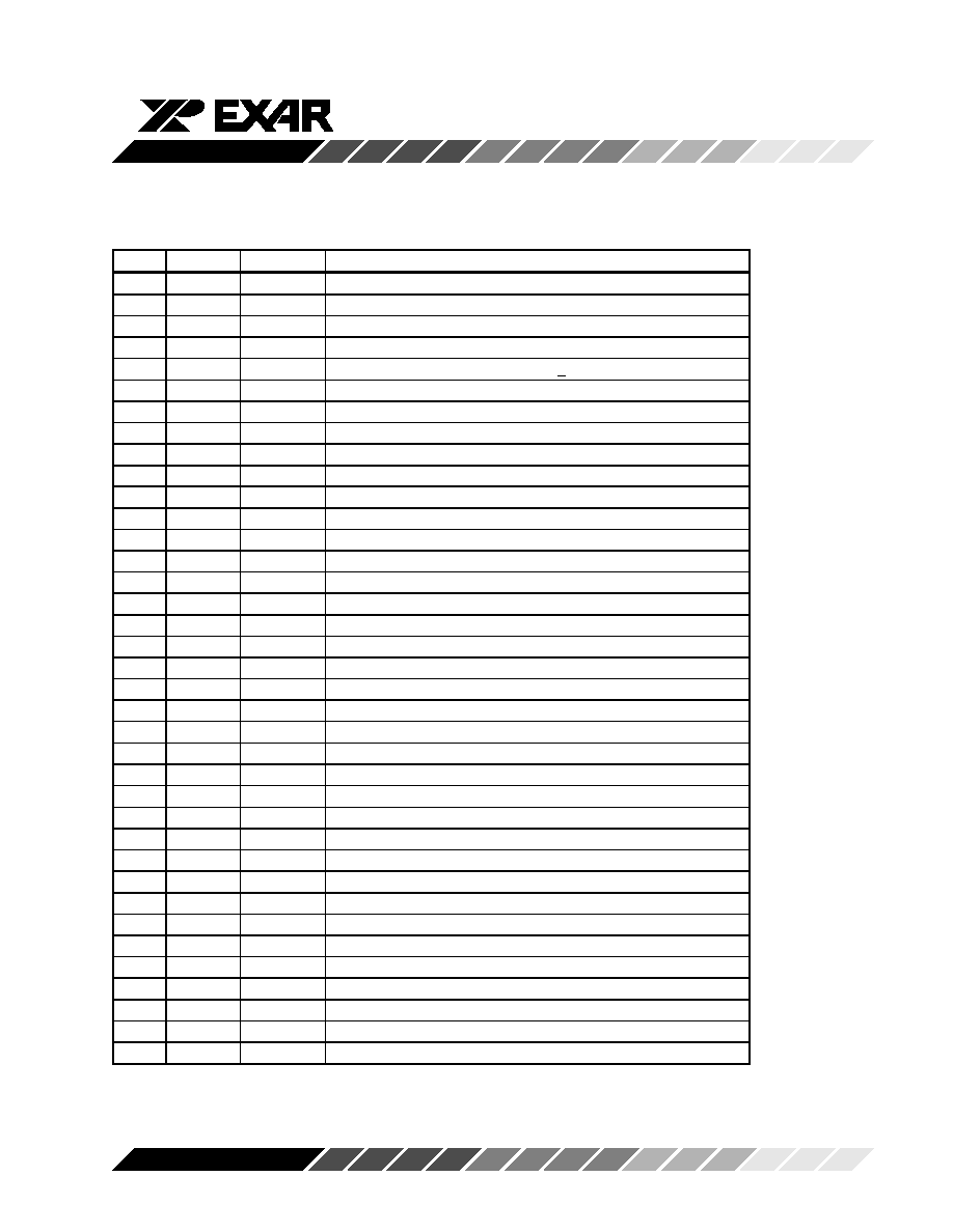
PIN DESCRIPTION
Pin #
Symbol
Type
Description
1
DB7
Digital Out
ADC Output
2
DB6
Digital Out
ADC Output
3
DB5
Digital Out
ADC Output
4
OGND
Ground
Digital Output Ground
5
OV
DD
Power
Digital Output Power Supply (must be < AV
DD
)
6
DB4
Digital Out
ADC Output
7
DB3
Digital Out
ADC Output
8
DB2
Digital Out
ADC Output
9
DB1
Digital Out
ADC Output
10
DB0
Digital Out
ADC Output (LSB)
11
Fsync
Digital In
Frame Sync Clock. Connect to DV
DD
.
12
CAL
Digital In
Calibration Control (clamp OB)
13
CLAMP
Digital In
DC-Restore Clamp Control
14
SBLK
Digital In
Sample Black CDS Clock
15
SPIX
Digital In
Sample Pixel CDS Clock
16
ADCLK
Digital In
ADC Clock
17
DV
DD
Power
On chip Logic Power Supply (must = AV
DD
)
18
DGND
Ground
On chip Logic Ground
19
AV
DD
Power
Analog Power Supply
20
AGND
Ground
Analog Ground
21
SCLK
Digital In
Serial Interface Shift Clock
22
LOAD
Digital In
Serial Interface Data Load
23
SDI
Digital In
Serial Interface Data Input
24
OE
Digital In
Output Enable Control 1=enable, 0=high-Z
25
PD
Digital In
Power Down Control 1=powerdown, 0=convert
26
RESET
Digital In
Reset Control 1=reset, 0=convert
27
AGND
Ground
Analog Ground
28
REFin
Analog
CCD Reference Signal
29
CCDin
Analog
CCD Input Signal
30
AV
DD
Power
Analog Power Supply
31
Test1
Analog
Direct PGA Input (inverting input)
32
Test2
Analog
Direct PGA Input (non-inverting input)
33
AGND
ground
Analog Ground
34
DAC1
Analog
Utility DAC 1 Output
35
DAC0
Analog
Utility DAC 0 Output
36
AV
DD
Power
Analog Power Supply
37
ADCinP
Analog
Direct ADC Input (non-inverting input)
5
Rev. P2.00
XRD98L62
Preliminary
DC ELECTRICAL CHARACTERISTICS ≠ XRD98L62
Unless otherwise specified: OV
DD
= DV
DD
=AV
DD
= 3.0V, Pixel Rate = 30MSPS, T
A
= 25∞C
Rext= 20KOhm
Symbol
Parameter
Min.
Typ.
Max.
Unit
Conditions
CDS Performance
CDSV
IN
Input Range
800
mV
PP
Pixel (V
BLK
- V
VIDEO
), (See Figure 2).
V
DARK
Maximum Dark Voltage Offset
250
mV
At any gain. (See Figure 2).
Vrst
Reset Pulse
500
mV
r
CLAMP
Clamp On Resistance
120
PGA Parameters
AV
MIN
Minimum Gain
0
dB
Gain Code = 0
AV
MAX
Maximum Gain
36
dB
Gain Code > 768
PGA n
Resolution
10
bits
Transfer function is linear steps in dB
PGA Step
Gain Step Size
0.047
dB
ADC Parameters (Measured in ADC Test Mode)SDI = 0010 001 0011 1000
ADC n
Resolution
12
bits
f
s
Max Sample Rate
30
MSPS
DNL
Differential Non-Linearity
-1
+0.75
1
LSB
V
ID
Full Scale Differential Input
+1.0
V
REF
ADC Reference Voltage
1
V
CapP - CapN =
V
REF