 | –≠–ª–µ–∫—Ç—Ä–æ–Ω–Ω—ã–π –∫–æ–º–ø–æ–Ω–µ–Ω—Ç: XRT4000 | –°–∫–∞—á–∞—Ç—å:  PDF PDF  ZIP ZIP |
XRT4000
Universal Multiprotocol
Serial Interface
November 1998-2
Rev. 1.00
EXAR Corporation, 48720 Kato Road, Fremont, CA 95538
(510) 668-7000
FAX (510) 668-7017
FEATURES
∑
Software-configurable multiprotocol serial
interface supporting:
V.35, V.36, EIA-530 (A), RS232
(V.28), X.21, RS449
∑
One chip fully integrated solution (Internal
termination)
∑
Contains 8 receivers and 8 transmitters for full
DTE and DCE support
∑
Glitch filters on the control signals (Optional)
∑
+5V, +12V, -6V power supplies required
∑
Full support of loopbacks, data & clock inversion,
and echoed clock in DTE and DCE modes
∑
Full support of most popular types of HDLC
controllers (single, double, and triple clocks
supported)
∑
Internal oscillator for standalone DTE loopback
testing
∑
Control signals can be registered and non-
registered
∑
Control signals can be tri-stated for bus-based
designs
∑
"Fail Safe" operation supported
∑
ESD Protection Over + 2kV Range
APPLICATIONS
∑
Data Service Units (DSU)
∑
Routers
∑
Access Multiplexers
GENERAL DESCRIPTION
The XRT4000 is a fully integrated multiprotocol serial
interface. It is a universal device because it supports
all of the popular serial physical interfaces such as
V.35, V.36, EIA-530 (A), RS232 (V.28), X.21 and
RS449. Furthermore it can easily be interfaced with
most common types of HDLC controllers. This
device contains 8 receivers and 8 transmitters. It is
a complete solution containing all of the required
source and load terminations in one 100 pin TQFP
package.
XRT4000 can be configured to operate in one of the
seven interfaces in either DTE and DCE modes of
operation and power down mode. It fully supports
echoed clock as well as clock and data inversion. An
elaborate set of loopbacks are supported in DTE and
DCE modes of operation. This eliminates the need
for external circuitry for loopback implementation.
The control signals such as RI, RL, DCD, DTR, DSR
are protected against glitches by internal filters.
These filters can be disabled. XRT4000 has an
internal oscillator which is used to create a clock
signal needed to conduct standalone diagnostics of
DTE equipment.
ORDER INFORMATION
Part No.
Package
Operating
Temperature Range
XRT4000CV
100 Pin TQFP
0
∞
C to +70
∞
C

XRT4000
Rev. 1.00
- 2 -
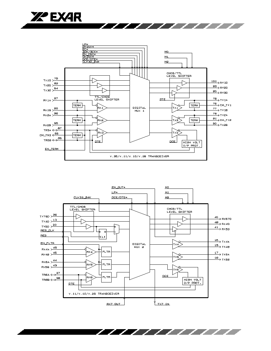
Figure 1. XRT4000 Functional Block Diagram
XRT4000
Rev. 1.00
- 3 -
Figure 2. XRT4000 RTMOD1 Block
Figure 3. XRT4000 RTMOD2 Block
XRT4000
Rev. 1.00
- 4 -
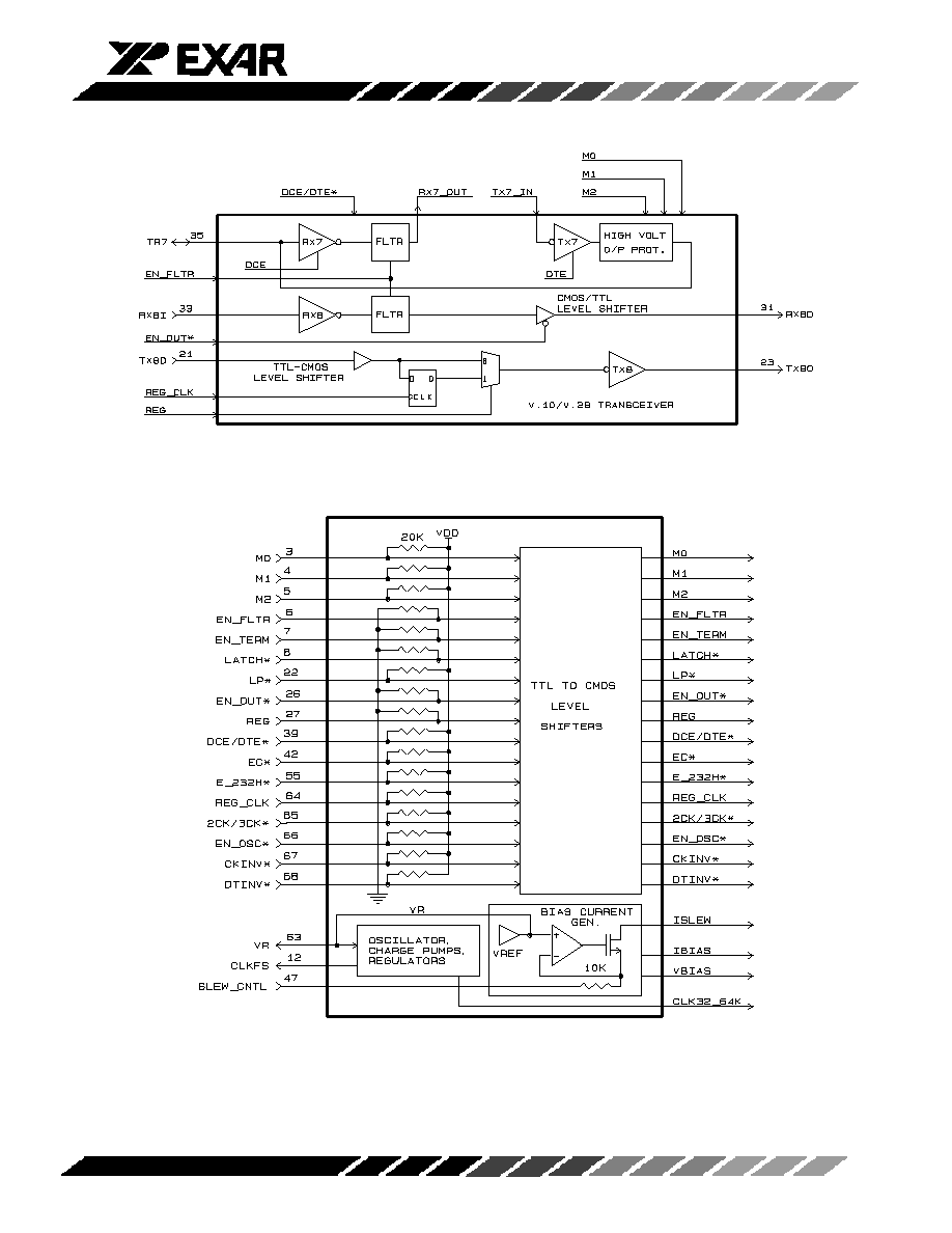
Figure 4. XRT4000 RTMOD3 Block
Figure 5. XRT4000 Control Block
Note: Signals without pin numbers having names identical to those with pin numbers are CMOS level-shifted
versions of TTL-compatible input signals.
XRT4000
Rev. 1.00
- 5 -
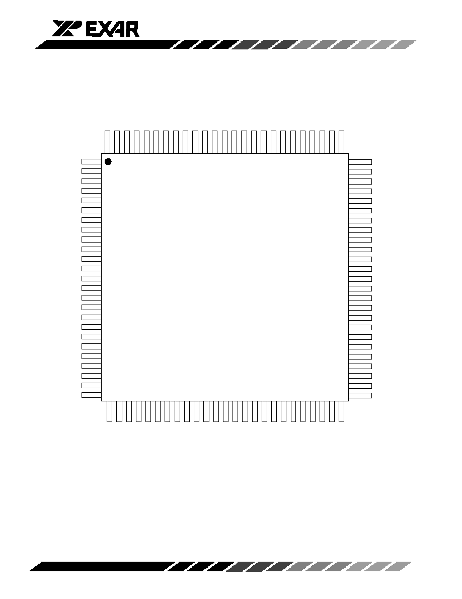
PIN CONFIGURATION
V D D
G N D
M 0
M 2
E N _ F L T R
E N _ T E R M
L A T C H *
V S S
V S S
G N D
C L K F S
M 1
T X 4 D
V D D
T X 4 B
T X 5 A
T X 4 A
T X 5 B
T X 8 D
G N D
T X 5 D
T X 8 O
V S S
L P *
V D D
T X 1 D
G N D
V S S
V D D
G N D
V S S
D T I N V *
C K I N V *
E N _ O S C *
2 C K / 3 C K *
R E G _ C L K
V D D
V R
V P P
N C
N C
N C
N C
E _ 2 3 2 H *
V P P
V D D
N / C
G N D
V S S
N / C
EN_OUT*
VSS
VDD
VDD
RX8D
GND
RX8I
TR7
VSS
TX76D
TR6A
TR6B
DCE/DTE*
RX67D
RX5D
EC*
RX5B
RX5A
RX4A
RX4B
SLEW_CNTL
RX4D
GND
N/C
REG
RX1D
VDD
RX1B
RX1A
RX2A
RX2B
VSS
RX2D
VDD
GND
RX3D
GND
TR3B
TR3A
CM_TR3
VSS
TX3D
VDD
TX2D
CM_TX2
TX2B
TX2A
TX1A
TX1B
CM_TX1
6 0
30
40
50
80
90
1 0
2 0
7 0
100-Pin
T Q F P
X R T 4 0 0 0

XRT4000
Rev. 1.00
- 6 -
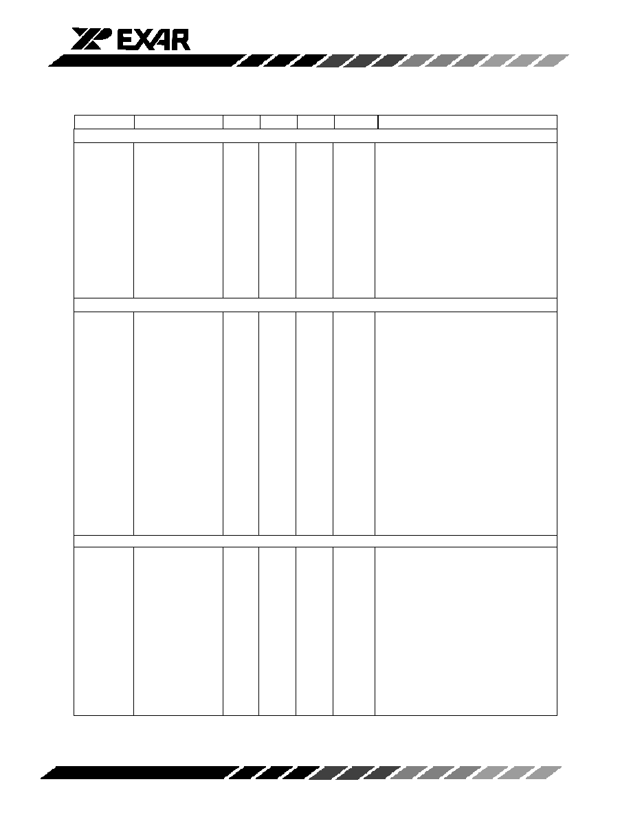
PIN DESCRIPTION
Pin
#
Symbol
DTE
Mode
DCE
Mode
Type
Function
1
VDD
Digital VDD for Receiver 1 - Connect to +5V
2
GND
Digital GND for Receiver 1
3
M0
I
Mode Control - Mode Select Input 0; Internal 20K
pull-up
4
M1
I
Mode Control - Mode Select Input 1; Internal 20K
pull-up
5
M2
I
Mode Control - Mode Select Input 2; Internal 20K
pull-up
6
EN_FLTR
I
Enable Glitch Filter on Receiver 4, 5, 6, 7, 8 inputs.
Internal 20K
pull-down
7
EN_TERM
I
Enable input termination for Receiver 1, 2, 3 in V.11 Mode.
Internal 20K
pull-down
8
LATCH*
I
Mode Control Input Latch Enable - Logic 0: Changes on
M0, 1, 2, EN_FLTR, and EN_TERM pins cause mode
changes (input latches in transparent state).
Logic 1: Changes on these input pins do not cause mode
changes (input latches in latched state). Internal 20K
pull-
down
9
VSS
Digital VSS for Transmitter 4, 5, 6. Connect to -6V
10
VSS
Analog VSS for bias generation Connect to -6V
11
GND
Digital GND for Transmitter 7, 8
12
CLKFS
O
Internal Clock Generated - 500kHz
13
TX4D
D_RTS
D_CTS
I
Transmitter 4 - Digital Data Input from equipment
14
VDD
Digital VDD for Transmitter 4, 5, 6; Connect to +5V
15
TX4B
RTSB
CTSB
O
Transmitter 4 - Positive Data Differential Output to line
16
TX4A
RTSA
CTSA
O
Transmitter 4 - Negative Data Differential Output to line
17
TX5A
DTRA
DSRA
O
Transmitter 5 - Negative Data Differential Output to line
18
TX5B
DTRB
DSRB
O
Transmitter 5 - Positive Data Differential Output to line
19
GND
Digital GND for Transmitter 4, 5, 6
20
TX5D
D_DTR
D_DSR
I
Transmitter 5 - Digital Data Input from equipment
21
TX8D
D_RL
D_RI
I
Transmitter 8 - Digital Data Input from equipment
22
LP*
I
Loopback Enable - Active low; Logic 0: Loopback
enabled.
Logic 1: Loopback disabled. Internal 20K
pull-up
23
TX8O
RLA
RIA
O
Transmitter 8 - Single Ended Data Output to line
24
VSS
Digital VSS for Transmitter 7, 8; Connect to -6V
25
VDD
Digital VDD for Transmitter 7, 8; Connect to +5V
26
EN_OUT*
I
Output Enable for Receiver 5, 8; Internal 20K
pull-down
27
REG
I
Register Control - Logic 1: TX5D, TX8D signal values will
be latched on the positive edge of REG_CLK, Logic 0: The
Register flip-flop is bypassed therefore REG_CLK has no
effect on these signals. Internal 20K
pull-down
28
VSS
Analog VSS for Receiver 4, 5, 6; Connect to -6V
29
VDD
Analog VDD for Receiver 4, 5, 6; Connect to +5V
30
VDD
Analog VDD for Receiver 7, 8; Connect to +5V
31
RX8D
D_RI
D_RL
O
Receiver 8 - Digital Data Output to equipment
32
GND
Analog GND for Receiver 7, 8
33
RX8I
RIA
RLA
I
Receiver 8 - Single Ended Data Input from line
34
VSS
Analog VSS for Receiver 7, 8; Connect to -6V
Note: An asterisk (*) following a pin symbol indicates that the pin is active low.
Names begining with D_ are digital signals.
Names ending with B and A are the positive and negative polarities of differential signals respectively.
XRT4000
Rev. 1.00
- 7 -
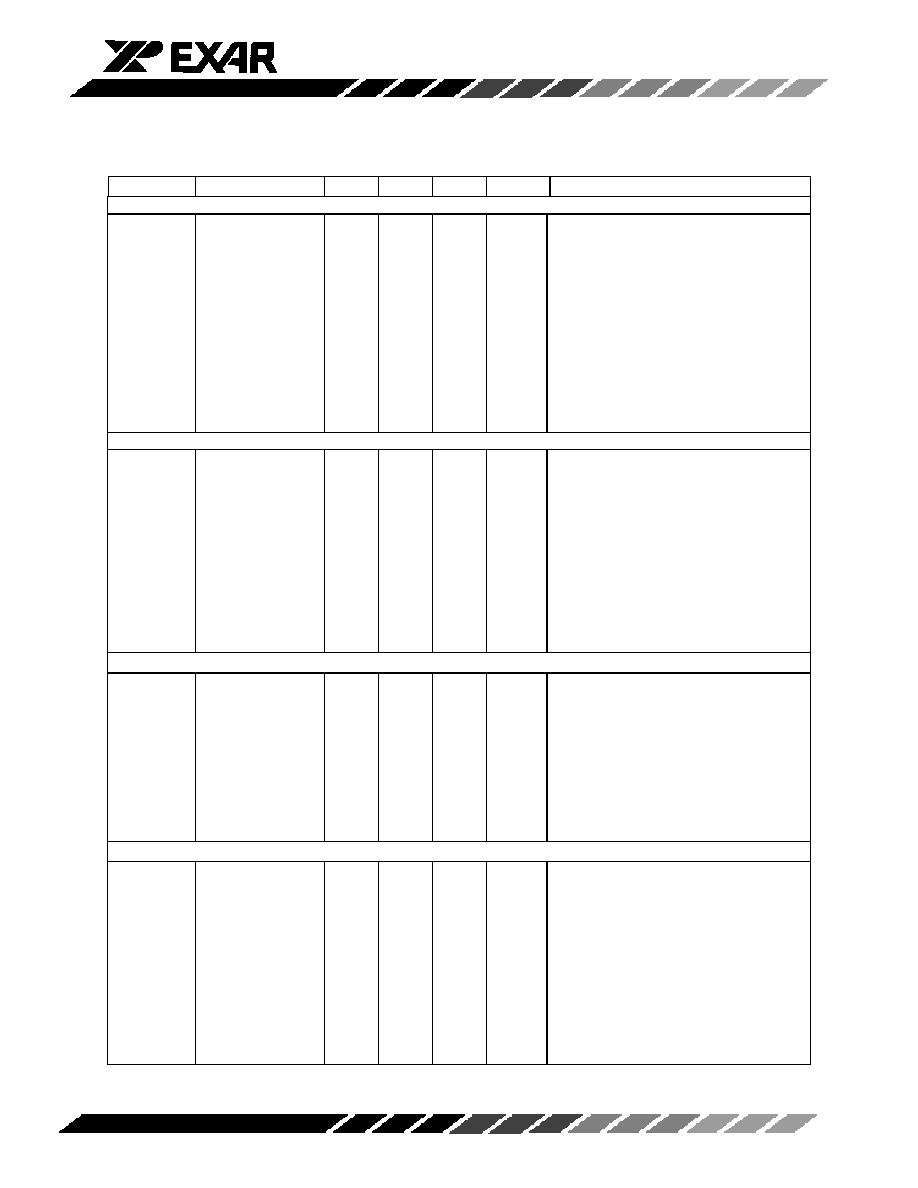
PIN DESCRIPTION (CONT'D)
Pin
#
Symbol
DTE
Mode
DCE
Mode
Type
Function
35
TR7
LLA
LLA
I/O
DTE Mode - Transmitter 7 - Single Ended Data Output to line
DCE Mode - Receiver 7 - Single Ended Data Input from line
36
TX76D
D_LL
D_DCD
I
Digital Input - Refer to Mode Control Table
37
TR6A
DCDA
DCDA
I/O
DTE Mode - Receiver 6 - Negative Data Differential Input
from line
DCE Mode - Transmitter 6 - Negative Data Differential
Output to line
38
TR6B
DCDB
DCDB
I/O
DTE Mode - Receiver 6 - Positive Data Differential Input from
line
DCE Mode - Transmitter 6 - Positive Data Differential Output
to line
39
DCE/DTE*
LOW
HIGH
I
DCE/DTE Select - Selects operating mode. Logic 0: DTE
Mode. Logic 1: DCE Mode. Internal 20K
pull-up
40
RX67D
D_DCD
D_LL
O
Digital Output - Refer to Mode Control Table
41
RX5D
D_DSR
D_DTR
O
Receiver 5 - Digital Data Output to equipment
42
EC*
I
Enable Clock Mode - Active Low, Logic 0: Echoed Mode.
Logic 1: Normal Mode. Internal 20K
pull-up
43
RX5B
DSRB
DTRB
I
Receiver 5 - Positive Data Differential Input from line
44
RX5A
DSRA
DTRA
I
Receiver 5 - Negative Data Differential Input from line
45
RX4A
CTSA
RTSA
I
Receiver 4 - Negative Data Differential Input from line
46
RX4B
CTSB
RTSB
I
Receiver 4 - Positive Data Differential Input from line
47
SLEW_
CNTL
O
Analog Output - Resistor connected between this pin and
Ground controls transmitter output pulse rise and fall time in
V.10 or V.28 mode as specified in Figures 15 and 16
respectively.
48
RX4D
D_CTS
D_RTS
O
Receiver 4 - Digital Data Output to equipment
49
GND
Digital GND for Receiver 4, 5, 6
50
NC
51
NC
52
GND
Analog GND for bias generator.
53
NC
54
VSS
Analog Substrate - Connect to -6V
55
E_232H*
I
High Speed RS-232 Enable - Logic 0: Enables high speed
RS-232 mode (drives 3K
in parallel with 1000pF at 256KHz).
Internal 20K
pull-up
56
VDD
Analog VDD for bias generation circuit; Connect to +5V
57
VPP
VPP - Connect to +12V supply
58
NC
59
NC
60
NC
61
NC
62
VPP
VPP - Connect to +12V supply
63
VR
O
VR - Internally generated +2.2V Reference (Sources 20
µ
A
maximum)
Note: An asterisk (*) following a pin symbol indicates that the pin is active low.
Names begining with D_ are digital signals.
Names ending with B and A are the positive and negative polarities of differential signals respectively
XRT4000
Rev. 1.00
- 8 -
Pin
#
Symbol
DTE
Mode
DCE
Mode
Type
Function
64
REG_CLK
I
Clock - For Transmitter 5, 8 input register. Internal 20K
pull-up
65
2CK/3CK*
I
2 or 3 Clock Select - Internal 20K
pull-up
Logic Don't Care: 1 Clock When Mode = X.21 (M2, M1, M0= 011)
Logic 0: 3 Clocks When Mode
X.21 (M2, M1, M0
011)
Logic 1: 2 Clocks When Mode
X.21 (M2, M1, M0
011)
66
EN_OSC*
I
Test Oscillator Enable - Active Low; Logic 0: Oscillator Enabled.
Logic 1: Oscillator Disabled. Internal 20K
pull-up
67
CKINV*
I
Invert Clock - Active Low; Logic 0: Clock Inverted.
Logic 1: Clock not Inverted. Internal 20K
pull-up
68
DTINV*
I
Invert Data - Active Low; Logic 0: Data Inverted.
Logic 1: Data not Inverted. Internal 20K
pull-up
69
VSS
Digital VSS for Transmitter 1, 2, 3 Output Drivers;
Connect to -6V
70
GND
Digital GND for Transmitter 1, 2, 3 Output Drivers
71
VDD
Digital VDD for Transmitter 1, 2, 3 Output Drivers;
Connect to +5V
72
VDD
Analog VDD for Transmitter 1, 2; Connect to +5V
73
VSS
Analog VSS for Transmitter 1, 2; Connect to -6V
74
GND
Analog GND for Transmitter 1, 2 "T" termination
75
TX1D
D_TXD
D_RXD
I
Transmitter 1- Digital Data Input from equipment
76
CM_TX1
O
AC GND - Transmitter 1 Output Termination center tap in V.35 mode
77
TX1B
TXDB
RXDB
O
Transmitter 1 - Positive Data Differential Output to line
78
TX1A
TXDA
RXDA
O
Transmitter 1 - Negative Data Differential Output to line
79
TX2A
SCTEA
RXCA
O
Transmitter 2 - Negative Data Differential Output to line
80
TX2B
SCTEB
RXCB
O
Transmitter 2 - Positive Data Differential Output to line
81
CM_TX2
O
AC GND - Transmitter 2 Output Termination center tap in V.35 mode
82
TX2D
D_SCTE
D_RXC
I
Transmitter 2 - Digital Data Input from equipment
83
VDD
Digital VDD for Receiver and Transmitter 1, 2, 3; Connect to +5V
84
TX3D
D_X
D_TXC
I
DTE Mode - Input not used
DCE Mode - Transmitter 3 - Digital Data Input from equipment
85
VSS
Digital VSS for Receiver and Transmitter 1, 2, 3; Connect to -6V
86
CM_TR3
O
DTE Mode - AC GND - Transmitter 3 Output Termination center tap
in V.35 mode
DCE Mode - AC GND - Receiver 3 Input Termination center tap in
V.35 mode
87
TR3A
TXCA
TXCA
I/O
DTE Mode - Receiver 3 - Negative Data Differential Input from line.
DCE Mode - Transmitter 3 - Negative Data Differential Output to
line.
Note: An asterisk (*) following a pin symbol indicates that the pin is active low.
Names begining with D_ are digital signals.
Names ending with B and A are the positive and negative polarities of differential signals respectively
XRT4000
Rev. 1.00
- 9 -
Pin
#
Symbol
DTE
Mode
DCE
Mode
Type
Function
88
TR3B
TXCB
TXCB
I/O
DCE Mode - Transmitter 3 - Positive Data Differential
Output to line
DTE Mode - Receiver 3 - Positive Data Differential Input
from line
89
GND
Analog GND for Receiver 1, 2, 3
90
RX3D
D_TXC
D_X
O
DTE Mode - Receiver 3- Digital Data Output to equipment
DCE Mode - Not used
91
VDD
Digital VDD for Receiver 2, 3; Connect to +5V
92
GND
Digital GND for Receiver 2, 3
93
RX2D
D_RXC
D_SCTE
O
Receiver 2 - Digital Data Output to equipment
94
VSS
Analog VSS for Receiver 1, 2, 3; Connect to -6V
95
RX2B
RXCB
SCTEB
I
Receiver 2 - Positive Data Differential Input from line
96
RX2A
RXCA
SCTEA
I
Receiver 2 - Negative Data Differential Input from line
97
RX1A
RXDA
TXDA
I
Receiver 2 - Negative Data Differential Input from line
98
RX1B
RXDB
TXDB
I
Receiver 2 - Positive Data Differential Input from line
99
VDD
Analog VDD for Receiver 1, 2, 3; Connect to +5V
100
RX1D
D_RXD
D_TXD
O
Receiver 1 - Digital Data Output to equipment
Note: An asterisk (*) following a pin symbol indicates that the pin is active low.
Names begining with D_ are digital signals.
Names ending with B and A are the positive and negative polarities of differential signals respectively.
`

XRT4000
Rev. 1.00
- 10 -
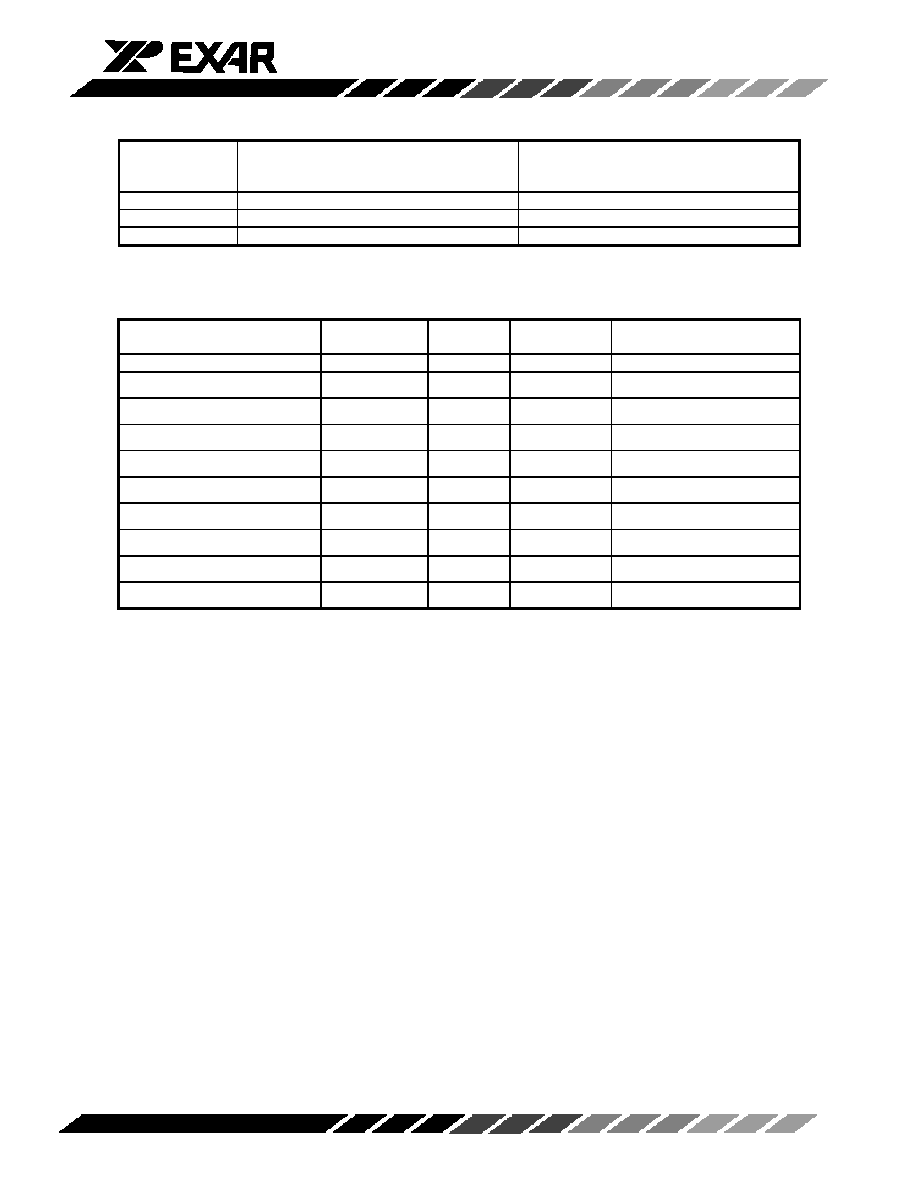
ELECTRICAL CHARCTERISTICS
Test Conditions: VDD = 5V, VSS = -6V, VPP = 12V (all
±
5%), TA = 25
∞
C
Sybol
Parameter
Min
Typ
Max
Unitd
Interface
Supply Currents
M0
M1
M2
I
DD
VDD
Supply
Current
20
mA
0
0
0
V.10, No Load
(DCE
Mode,
90
mA
0
0
0
V.10, Full Load
All Digital
Pins=GND
20
mA
1
0
0
EIA-530A, No Load
or VDD)
160
mA
1
0
0
EIA-530A, Full Load
55
mA
0
0
1
V.35, No Load on V.28 Drivers
55
mA
0
0
1
V.35, Full Load on V.28
Drivers
16
mA
0
1
1
RS232, No Load
16
mA
0
1
1
RS232, Full Load
2
mA
1
1
1
Power Down Mode
I
SS
VSS
Supply
Current
30
mA
0
0
0
V.10, No Load
(DCE
Mode,
90
mA
0
0
0
V.10, Full Load
All Digital
Pins=GND
30
mA
1
0
0
EIA-530A, No Load
or VDD)
50
mA
1
0
0
EIA-530A, Full Load
45
mA
0
0
1
V.35, No Load on V.28 Drivers
55
mA
0
0
1
V.35, Full Load on V.28
Drivers
16
mA
0
1
1
RS232, No Load
30
mA
0
1
1
RS232, Full Load
2
mA
1
1
1
Power Down Mode
I
PP
VPP
Supply
Current
10
mA
0
0
0
V.10, No Load
(DCE
Mode,
10
mA
0
0
0
V.10, Full Load
All Digital
Pins =
GND
10
mA
1
0
0
EIA-530A, No Load
or VDD)
10
mA
1
0
0
EIA-530A, Full Load
10
mA
0
0
1
V.35, No Load on V.28 Drivers
20
mA
0
0
1
V.35, Full Load on V.28
Drivers
10
mA
0
1
1
RS232, No Load
25
mA
0
1
1
RS232, Full Load
10
mA
1
1
1
Power Down Mode
Note 1: Absolute Maximum Ratings are those beyond which the safety of a device may be impaired.
Note 2: All currents into device pins are positive; all currents out of device are negative. All voltages are
referenced to device ground unless otherwise specified.
XRT4000
Rev. 1.00
- 11 -
ELECTRICAL CHARCTERISTICS (CONT'D)
Test Conditions: VDD = 5V, VSS = -6V, VPP = 12V (all
±
5%), TA = 25
∞
C
Symbol
Parameter
Min
Typ
Max
Units
Conditions
Logic Inputs and Outputs
V
IH
Logic Input High
Voltage
2
V
V
IL
Logic Input Low
Voltage
0.8
V
I
IN
Logic Input
Current
±250
µ
A
With 20k
internal pull-up/down resistor
V
OH
Output High
Voltage
3
4.5
V
IO = -4mA
V
OL
Output Low
Voltage
0.3
0.8
V
IO = 4mA
I
OSR
Output Short-
Circuit Current
-60
60
mA
0V
VO
VDD
I
OZR
Three-State
Output Current
0
±1
µ
A
M0 = Ml = M2 = VDD 0V
VO
VDD
V.11 Driver
V
OD
Differential Output
Voltage
±2
5
V
Open Circuit
RL = 50
(Figure 6)
V
OD
Change in
Magnitude of
Differential Output
Voltage
0.2
V
RL = 50
(Figure 6)
V
OC
Common Mode
Output Voltage
3.0
V
RL = 50
(Figure 6)
V
OC
Change in
Magnitude of
Common Mode
Output Voltage
0.2
V
RL = 50
(Figure 6)
I
SS
Short-Circuit
Current
±150
mA
VO = GND
I
OZ
Output Leakage
Current
±0.01
±100
µ
A
-0.25V
VO
0.25V, Power Off or
Driver Disabled
t
r
, t
f
Rise or Fall Time
4
13
25
ns
(Figures 7, 11)
T
PLH
Input to Output
50
70
110
ns
(Figures 7, 11)
T
PHL
Input to Output
50
70
110
ns
(Figures 7, 11)
t
Inp. to Out.
Difference, |TPLH
- TPHL|
0
5
15
ns
(Figures 7, 11)
T
SKEW
Output to Output
Skew
5
ns
(Figures 7, 11)
Note 1: Absolute Maximum Ratings are those beyond which the safety of a device may be impaired.
Note 2: All currents into device pins are positive; all currents out of device are negative. All voltages are
referenced to device ground unless otherwise specified.
XRT4000
Rev. 1.00
- 12 -
ELECTRICAL CHARCTERISTICS (CONT'D)
Test Conditions: VDD = 5V, VSS = -6V, VPP = 12V (all
±
5%), TA = 25
∞
C
Symbol
Parameter
Min
Typ
Max
Units
Conditions
V.11 Receiver
V
TH
Input Threshold
Voltage
-0.2
0.2
-7V
VCM
7V
VTH
Input Hysteresis
35
60
mV
-7V
VCM
7V
I
IN
Input Current (A,
B)
±1
±1.5
mA
-10V
VA,B
10V
R
IN
Input Impedance
9
10
11
k
-10V
VA,B
10V
t
r
, t
f
Rise or Fall Time
20
ns
(Figures 7, 12)
T
PLH
Input to Output
50
80
120
ns
(Figures 7, 12)
T
PHL
Input to Output
50
80
120
ns
(Figures 7, 12)
t
Inp. to Out.
Difference, |TPLH
- TPHL|
0
5
15
ns
(Figures 7, 12)
V.35 Driver
V
OD
Differential Output
Voltage
±0.44
±0.55
±0.66
V
With Load, (Figure 12)
I
OH
Transmitter
Output High
Current
-12
-11
-10
mA
VA, B = 0V
I
OL
Transmitter
Output Low
Current
10
11
12
mA
VA, B = 0V
I
OZ
Transmiter Output
Leakage Current
±0.01
±100
µ
A
-0.25
VA,B
0.25V
t
r
, t
f
Rise or Fall Time
5
ns
(Figures 8, 11)
T
PLH
Input to Output
25
55
85
ns
(Figures 8, 11)
T
PHL
Input to Output
25
55
85
ns
(Figures 8, 11)
t
Inp. to Out.
Difference, |TPLH
- TPHL|
0
5
15
ns
(Figures 8, 11)
T
SKEW
Output to Output
Skew
5
ns
(Figures 8, 11)
V.35 Receiver
V
TH
Differential Input
Threshold Volt.
-0.2
0.2
V
-2V
=
(VA + VB)/2
=
2V (Figure 8)
V
TH
Input Hysteresis
35
60
mV
-2V
=
(VA + VB)/2
=
2V (Figure 8)
I
IN
Input Current
(A,B)
±60
mA
-10V
=
VA, B
=
10V
R
IN
Input Impedance
(A, B)
175
-10V
=
VA, B
=
10V
t
r
, t
f
Rise or Fall Time
20
ns
(Figures 8, 12)
T
PLH
Input to Output
80
120
ns
(Figures 8, 12)
T
PHL
Input to Output
100
120
ns
(Figures 8, 12)
t
Input to Output
Difference, ITPLH
- TPHLI
5
15
ns
(Figures 8, 12)
Note 1: Absolute Maximum Ratings are those beyond which the safety of a device may be impaired.
Note 2: All currents into device pins are positive; all currents out of device are negative. All voltages are
referenced to device ground unless otherwise specified.
XRT4000
Rev. 1.00
- 13 -
ELECTRICAL CHARCTERISTICS (CONT'D)
Test Conditions: VDD = 5V, VSS = -6V, VPP = 12V (all
±
5%), TA = 25
∞
C
Symbol
Parameter
Min
Typ
Max
Units
Conditions
V.10 Driver
V
O
Output Voltage
±4.0
±3.6
±6.0
V
V
Open Circuit, RL = 3.9k
RL = 450
(Figure 9)
I
SS
Short-Circuit
Current
±100
mA
VO = GND
I
OZ
Input Leakage
Current
±0.1
±100
µ
A
-0.25
VO
0.25V, Power Off or
Driver Disabled
t
r
, t
f
Rise or Fall Time
0
5
µ
s
(Figures 9, 13), RL = 450
, CL = 100pF
RSLEW_CNTL = 10k
T
PLH
Input to output
5
µ
s
(Figures 9, 13), RL = 450
, CL = 100pF
RSLEW_CNTL = 10k
T
PHL
Input to output
5
µ
s
(Figures 9, 13), RL = 450
, CL = 100pF
RSLEW_CNTL = 10k
V.10 Receiver
V
TH
Receiver Input
Threshold Voltage
-0.2
0.2
V
AV
TH
Receiver Input
Hysteresis
35
60
mV
I
IN
Receiver Input
Current
±1
±1.5
mA
-10
VA
10V
R
IN
Receiver Input
Impedance
9
10
11
k
-10
VA
10V
t
r
, t
f
Rise or Fall Time
20
ns
(Figures 10, 14)
T
PLH
Input to Output
100
ns
(Figures 10, 14)
T
PHL
Input to Output
100
ns
(Figures 10, 14)
V.28 Driver
V
O
Output Voltage
±5
±5.5
±6
V
Open Circuit
RL = 3k (Figure 9)
I
SS
Short-Circuit
Current
±100
mA
VO = GND
I
OZ
Input Leakage
Current
±0.01
±100
µ
A
-0.25
VCM
0.25V, Power Off or
Driver Disabled
SR
Slew Rate
4.0
30.0
V/
µ
s
(Figures 9, 13), RL = 3k, CL = 2500pF
T
PLH
Input to output
2
4
µ
s
(Figures 9, 13), RL = 3k, CL = 2500pF
T
PHL
Input to output
2
4
µ
s
(Figures 9, 13), RL = 3k, CL = 2500pF
V.28 Receiver
V
THL
Input Low
Threshold Voltage
1.4
0.8
V
V
TLH
Input High
Threshold Voltage
2.0
1.4
V
AV
TH
Receiver Input
Hysteresis
0.1
0.4
1.0
V
R
IN
Receiver Input
Impedance
3
5
7
k
-15
VA
15V
t
r
, t
f
Rise or Fall Time
20
ns
(Figures 10, 14)
T
PLH
Input to Output
120
ns
(Figures 10, 14)
T
PHL
Input to Output
180
ns
(Figures 10, 14)

XRT4000
Rev. 1.00
- 14 -
The following tests circuits and timing diagrams are referenced in the preceding Electrical Characteristics
Tables.
Figure 6. RS422 Driver Test Circuit
Figure 7. RS422 Driver/Receiver AC Test Circuit
Figure 8. V.35 Driver/Receiver AC Test Circuit (TX1/RX1, TX2/RX2 Only)
Figure 9. V.10/V.28 Driver Test Circuit
Figure 10. V.10/V.28 Receiver Test Circuit

XRT4000
Rev. 1.00
- 15 -
Figure 11. V.11, V.35 Driver Propagation Delays
V1 = 0V for V.35, 2.5V for V.11
Figure 12. V.11, V.35 Receiver Propagation Delays
Figure 13. V.10, V.28 Driver Propagation Delays
V1 = 1.8V for V.28, 0.1V for V.10
V2 = 1.0V for V.28. -0.1V for V.10
Figure 14. V.10, V.28 Receiver Propagation Delays

XRT4000
Rev. 1.00
- 16 -
SYSTEM DESCRIPTION
It is important to describe the difference
between an electrical specification and a
physical interface specification. An electrical
specification defines the electrical characteristics
of a transmitter or receiver. These include
voltage, current, impedance levels, rise/fall
times and other similar parameters. Popular
electrical interfaces are V.10, V.11, V.35 and
V.28. A serial physical interface specification,
however, describes an interface in its entirety.
This description includes the names and
functions of all involved signals, the electrical
parameters of each of the signals, and the
connector type. Popular serial interface types
include V.35, RS232 (V.28), RS449, EIA-530(A),
X.21, and V.36. The XRT4000 contains a
sufficient number of receivers, transmitters and
transceivers to transport all of the signals
required for a physical serial interface. It has
control circuitry that can configure each driver
and receiver to the appropriate electrical levels
required by the specification for the selected
serial interface.
Figure 1 is a top level block diagram that shows
how the eight receivers and eight transmitters
present in the XRT4000 are grouped in three
modules named RTMOD1, RTMOD2, and
RTMOD3. A forth module labeled CONTROL
programs these receivers and transmitters with
the appropriate electrical levels for operation
with most popular standard serial interfaces
such as V.35, RS232, RS449, EIA-530(A), X.21,
and V.36. These interfaces are fully compliant
with international NET1 and NET2
specifications.
Figures 2, 3, 4, and 5 are a set of functional
block diagrams that give more detailed
information about the four modules shown in the
top-level diagram. The eight receivers and
transmitters are grouped in three different
categories according to the type of signals
transmitted or received. The categories are
denoted as RTMOD1 (Figure 2), RTMOD2
(Figure 3), RTMOD3 (Figure 4), and CONTROL
(Figure 5).
RTMOD1 Block
RTMOD1 is intended for the high speed data
and clock signals of a selected interface. This
block contains receivers RX1 and RX2,
transmitters TX1 and TX2, and bi-directional
transceiver TR3 which is composed of TX3 and
RX3. All of these devices may be programmed
with the electrical levels required for V.35, V.11,
V.10, or V.28 operating modes. In V.35 mode,
each transmitter has a common mode pin that is
connected to the center of the internal
termination. This pin should be bypassed to
ground with an external capacitor in order to
provide the best possible driver output stage
balance. In a system application, the TX1-RX1
pair and TX2-RX2 pair handle the TXD-RXD and
TXC-RXC high-speed interface signals
respectively. Transceiver TR3 is dedicated to
the SCTE signal for both DCE and DTE modes
of operation. It functions as a receiver for the
DTE mode and as a transmitter during the DCE
mode.
RTMOD2 Block
RTMOD2 contains receivers RX4 and RX5,
transmitters TX4 and TX5, and transceiver TR6
which is composed of TX6 and RX6. These
devices may be programmed with the electrical
levels required for V.11, V.10, or V.28 operating
modes. The RX4-TX4 pair are dedicated for
RTS and CTS signals while RX5-TX5 are
intended for DTR and DSR signals. Transceiver
TR3 handles the DCD signal which requires a
transmitter in the DCE and a receiver
in-the-
DTE mode.
RTMOD3 Block
RTMOD3 contains transceiver TR7, which is
composed of TX7 and RX7, receiver RX8 and
transmitter TX8. These devices, which may be
programmed with the electrical levels required
for V.10, or V.28 operating modes, are intended
for the LL, RL and RI signals.

XRT4000
Rev. 1.00
- 17 -
CONTROL Block
The CONTROL block contains the configuration
and bias generation circuitry required by
RTMOD1, RTMOD2, and RTMOD3. It includes
TTL to CMOS level shifters for the control signal
inputs which have either an internal 20 k
pull-
up or pull-down resistor as shown in Figure 5
and as described in the pin description. This
block also includes a reference voltage source,
bias voltage and current generators, and a slew
rate control circuit that is used in the V.10 and
V.28 modes. The physical interface
configuration is done by three control pins called
M0, M1 and M2. The logic levels present on
these three inputs are internally latched during a
positive transition of the LATCH* signal. The
functions of the eight possible combinations of
M0, M1 and M2 are described in Tables 1 and 2.
Power Requirements
Table 3, which contains the maximum and
minimum peak supply currents for each of the 3
supply voltages, provides the information
necessary for determining a system power
budget. Notice that maximum current is
required in the V.11 mode when TX1, TX2, and
TX3 are terminated with 100
. Minimum current
consumption occurs when none of the
transmitters are terminated and the device is not
in the V.35 mode.
Receiver and Transmitter Specifications
Tables 4 and 5, which are for the XRT4000
receiver and transmitter sections respectively,
summarize the electrical requirements for V.35,
V.11, V.10, and RS232 interfaces. These tables
provide virtually all of the electrical information
necessary to describe these 4 interfaces in a
concise form.

XRT4000
Rev. 1.00
- 18 -
CONTROL
DRIVER/RECEIVER PAIR AND CORRESPONDING SIGNAL NAME - DTE MODE
INTERFACE
INPUTS
TX1
RX1
TX2
RX2 TX3 RX3
TX4
RX4
TX5
RX5
TX6
RX6
TX7
RX7
TX8 RX8 STANDARD
M2
M1
M0
TXD
RXD SCTE
RXC
-
TXC
RTS
CTS
DTR
DSR
-
DCD
LL
TM
RL
RI
0
0
0
10
10
10
10
Off
10
10
10
10
10
Off
10
10
Off
10
10
V.10
0
0
1
11
11
11
11
Off
11
11
11
10
10
Off
11
10
Off
10
10
EIA-530-A
0
1
0
11
11
11
11
Off
11
11
11
11
11
Off
11
10
Off
10
10
EIA-530, RS449, V.36
0
1
1
11
11
11
11
Off
11
11
11
11
11
Off
Off
Off
Off
Off
Off X.21
1
0
0
35
35
35
35
Off
35
28
28
28
28
Off
28
28
Off
28
28
V.35
1
0
1
11
11
11
11
Off
11
11
11
11
11
Off
11
10
Off
10
10
RESERVED
1
1
0
28
28
28
28
Off
28
28
28
28
28
Off
28
28
Off
28
28
RS232
1
1
1
Off
Off
Off
Off
Off
Off
Off
Off
Off
Off
Off
Off
Off
Off
Off
Off POWER DOWN
Table 1. DTE Mode - Control Programming for Driver and Receiver Mode Selection
CONTROL
DRIVER/RECEIVER PAIR AND CORRESPONDING SIGNAL NAME - DCE MODE
INTERFACE
INPUTS
TX1
RX1
TX2
RX2
TX3
RX3
TX4
RX4
TX5
RX5
TX6
RX6
TX7
RX7
TX8
RX8
STANDARD
M2
M1 M0 RXD TXD RXC SCTE TXC
-
CTS
RTS
DSR
DTR
DCD
-
TM
LL
RI
RL
0
0
0
10
10
10
10
10
Off
10
10
10
10
10
Off
Off
10
10
10
V.10
0
0
1
11
11
11
11
11
Off
11
11
10
10
11
Off
Off
10
10
10
EIA-530-A
0
1
0
11
11
11
11
11
Off
11
11
11
11
11
Off
Off
10
10
10
EIA-530, RS449, V.36
0
1
1
11
11
11
11
11
Off
11
11
11
11
OFF
Off
Off
Off
Off
Off
X.21
1
0
0
35
35
35
35
35
Off
28
28
28
28
28
Off
Off
28
28
28
V.35
1
0
1
11
11
11
11
11
Off
11
11
11
11
11
Off
Off
10
10
10
RESERVED
1
1
0
28
28
28
28
28
Off
28
28
28
28
28
Off
Off
28
28
28
RS232
1
1
1
Off
Off
Off
Off
Off
Off
Off
Off
Off
Off
Off
Off
Off
Off
Off
Off
POWER DOWN
Table 2. DCE Mode - Control Programming for Driver and Receiver Mode Selection
Note: For the above tables:
Table
Representation
Corresponding
Electrical Level
Type
Signal
35
V.35
Differential
11
V.11
Differential
10
V.10
Single Ended
28
V.28/RS232
Single Ended
XRT4000
Rev. 1.00
- 19 -
Supply
Maximum Current
TX1-TX3 Drivers Terminated
with 100
in V.11 Mode
Minimum Current
None of the Drivers Terminated
(Non-V.35 Mode)
VDD (+5V)
160 mA
15 mA
VSS (-6V)
120 mA
20 mA
VPP (+12V)
40 mA
10 mA
Table 3. Maximum and Minimum Peak Supply Currents
V.35
V.11
V.10
RS232
Single-Ended or Differential
DIFF
DIFF
Single-Ended
Single-Ended
Max Signal Level
±
660 mV
±
6 V
±
6 V
±
15 V
Min Signal Level
±
440 mV
±
300 mV
±
300 mV
±
3 V
Common-Mode Voltage
±
2 V
±
7 V
Note 1
N/A
Max Signal Peak Operation
±
2.66 V
±
10 V
±
10 V
±
15 V
Max Signal Peak no Damage
N/A
±
12 V
±
12 V
±
25 V
Rin Differential
100
±
10%
Note 2
N/A
N/A
Rin Common-Mode
150
±
15%
N/A
N/A
N/A
DC Rin Each Input to Ground
> 8K
> 8K
> 8K
3K
< DC Rin < 7 K
Clock Frequency
20 MHz
20MHz
120KHz
256KHz
Table 4. Receiver Specifications
Note 1:
±
7 V on Receivers 1-6, not applicable for Receivers 7-8
Note 2: 100 to 150 Ohms terminated.
XRT4000
Rev. 1.00
- 20 -
V.35
V.11
V.10
RS232
Single-Ended or Differential
DIFF
DIFF
Single-Ended
Single-Ended
Max Signal Level
±
660 mV
RL= 100
|
V0
|
< 6 V
RL=3900
4 <
|
V0
|
< 6 V
RL=3900
±
6 V
3000
< RL <
7000
Min Signal Level
±
440 mV
RL= 100
2V <
|
VT
|
>0.5 V0
RL=100
|
VT
|
> 0.9 V0
RL= 450
±
5 V
3000
< RL <
7000
Offset Voltage
N/A
|
Vos
|
< 3V
N/A
N/A
Rout Differential
100
±
10%
100
N/A
N/A
Rout Common-Mode
150
±
15%
N/A
N/A
N/A
Rout Power Off
N/A
N/A
N/A
> 300
Output Slew Rate/Tr,Tf
20 ns
20 ns
1ms
< 30 V/
µ
s
Clock Frequency
20 MHz
20 MHz
120 KHz
256 KHz
Table 5. Transmitter Specification
V.10\V.28 Output Pulse Rise and Fall Time
SLEW_CNTL (pin 47) is an analog output that
controls transmitter pulse rise and fall time for
the V.10 and V.28 modes. Connecting a
resistor, RSLEW, having a value between 0 and
200 k
from this pin to ground controls the
rise/fall times for V.10 and the slew rate for V.28
as shown in Figures 15 and 16 respectively.
High-Speed RS232 Mode
When E_232H* (pin 55) is set to logic 0 in
RS232 mode, the transmitters are put is a
special high-speed RS232 mode that can drive
loads of 3000
in parallel with 1000pF at
speeds up to 256 KHz.
Power Down Mode
All transmitters and receivers may be powered
down by either setting the pins for control bits
M0, M1 and M2 to logic 1 or by leaving them
open.
Internal Cable Terminations
XRT4000 has fully integrated receiver and
transmitter cable terminations for high speed
signals (RXD, TXD, RXC, TXC, SCTE).
Therefore, no external resistors and/or switches
are necessary to implement the proper line
termination. The schematic diagrams given in
Figures 17 and 18 show the effective receiver
and transmitter terminations respectively for
each mode of operation. When a specific
electrical interface is selected by M0, M1 and
M2, the termination required for that interface is
also automatically chosen. The XRT4000
eliminates double termination problems and
makes point to multipoint operation possible in
the V.11 mode by providing the option for
disabling the internal input termination on high
speed receivers.
Glitch Filters
Occasional extraneous glitches on
control/handshake signal inputs such as CTS,
RTS, DTR and DSR can have damaging effects
on the integrity of a connection. The XRT4000
is equipped with lowpass filters on the input of
each of the receivers for the control and
handshake signals. These filters eliminate
glitches which are narrower than 10
µ
s. The
user may disable these filters by setting
EN_FLTR to logic 0.

XRT4000
Rev. 1.00
- 21 -
Clock Inversion
Transmit Clock signal, TXC, has an inversion
option for both DTE and DCE modes of
operation. The user can invert the polarity of the
TXC by setting CKINV* to logic 0. In the DTE
mode, the incoming TXC signal from the line will
be inverted before it is routed to the system. In
DCE mode, the incoming TXC signal from the
system will be inverted before it is sent over the
line toward the remote DTE. This feature allows
a phase correction when there is a long cable
delay between the DTE and DCE. This
correction may be necessary in order to obtain
the desired clock-to-data phase relationship.
Data Inversion
Similar to TXC, there is a provision in the
XRT4000 to invert the TXD and RXD signals.
Once the Setting the DTINV* input to logic 0
enables an inverter at the output of RX1 and
input of TX1.
Registered Mode of Operation
The XRT4000 has integrated registers allowing
users the option of clocking the values of
DSR/DTR and RL/RI signals. This can be done
if the registered mode of operation is selected
(REG=1). In this case, the values of these
signals will be latched on the positive edge of
the REG_CLK signal. In the normal mode (REG
= 0), the registers on the path of the DSR/DTR
and RL/RI are bypassed and REG_CLK will
have no effect.
Similarly, the outputs of the receivers (RX5 and
RX8) can be disabled by setting the EN_OUT*
input high. This allows these drivers to be
connected directly to a microcontroller bus since
they can be enabled during read cycles and
disabled in other times.
This feature eliminates the need for external
registers when a microcontroller is used to
control (reading and writing) DSR/DTR and
RL/RI signals.
Loopbacks
XRT4000 contains internal logic to place the
interface in a loopback mode for test purposes.
The loopback feature is supported in both DTE
and DCE modes of operation and it can be
invoked by setting the LP* input at logic 0.
Possible loopback implementations are depicted
in the scenarios located at the end of this
document.

XRT4000
Rev. 1.00
- 22 -
10
100
1 10
3
1
10
100
1 10
3
R (K Ohms)
V.10 Rise Time (us)
Figure 15. V.10 Rise Time as a Function of RSLEW
10
100
1 10
3
0.01
0.1
1
10
R (K Ohms)
V.28 Slew Rate (V/us)
Figure 16. V.28 Slew Rate Over
±
3 V Output Range
with 3 k
in Parallel with 2500 pF Load as a Function of RSLEW

XRT4000
Rev. 1.00
- 23 -
Echoed Clock
The XRT4000 can interface with serial
controllers which have two or three clock pins.
Furthermore, it can handle interfaces (e.g. X.21)
which have only one clock. Information
contained in the Pin Description for the EC* and
2CK/3CK* pins shows how the user can select
the number of available clocks by applying the
appropriate logic levels to these inputs.
Self-contained DTE Loopback Testing
Equipment having a DTE interface obtains
timing information from another interface (DCE).
RXC and TXC are clocks which are sourced by
the DCE. A DTE device uses them to clock
data in/out of the interface. The SCTE clock is
generated by DTE using TXC or RXC which are
originated in the DCE. In summary, a DTE
equipment is a timing slave.
Occasionally it is beneficial to conduct testing of
a DTE interface without connecting it to its DCE
counterpart. Lack of a synchronization source
will make the standalone testing of DTE
equipment not possible. The XRT4000 has an
on-board oscillator which can be used as a
timing source while the DCE connection is
missing. This feature allows users to conduct
loopback testing on isolated equipment with a
DTE interface.
This mode is invoked if EN_OSC* is set to logic
0. This connects an internally generated clock
signal (32 kHz - 64 kHz) to the RX2D/RX3D
output. A standalone system test may be
performed by combining this feature with the
appropriate loopback mode.
Operational Scenarios
Visualizing features such as clock/data
inversion, echoed clock, and loopbacks, in DTE
and DCE modes makes configuring the
XRT4000 a non-trivial task. A series of 48
system level application diagrams located at the
end of the data sheet called "Scenarios" assist
users in understanding the benefits of these
different features. The internal XRT4000
connections required for a particular scenario
are made through MUX1 and MUX2 that are
shown on the block diagrams given in Figures 2
and 3 respectively. Table 6 contains the signal
routing information versus control input logic
level for MUX1 and Table 7 contains similar
information for MUX2.

XRT4000
Rev. 1.00
- 24 -
APPLICATIONS INFORMATION
Traditional interfaces either require different
transmitters and receivers for each electrical
standard, or use complicated termination
switching methods to change modes of
operation. Mechanical switching schemes,
which are expensive and inconvenient, include
relays, and custom cables with the terminations
located in the connectors. Electrical switching
circuits using FETs are difficult to implement
because the FET must remain off when the
signal voltage exceeds the supply voltage and
when the interface power is off.
The XRT4000 uses innovative, patented circuit
design techniques to solve the termination
switching problem. This device includes internal
circuitry that may be controlled by software to
provide the correct terminations for V.10
(RS423), V.11 (RS422), V.28 (RS232), and V.35
electrical interfaces. The schematic diagrams
given in Figures 17 and 18 conceptually show
the switching options for the high-speed receiver
input and transmitter output terminations
respectively. Additionally, Tables 4 and 5
provide a summary of receiver and transmitter
specifications respectively for the different
electrical modes of operation.
V.10 (RS423) Interface
Figure 19 shows a typical V.10 (RS423)
interface. This configuration uses an
unbalanced cable to connect the transmitter
TXA output to the receiver RXA input. The "B"
outputs and inputs that are present on the
differential transmitters and receivers contained
in the XRT4000 are not used. The system
ground provides the signal return path. The
receiver input resistance is 10 k
nominal and
no other cable termination is normally used for
the V.10 mode.
V.11 (RS422) Interface
Figure 11 shows a typical V.11 (RS422)
interface. This configuration uses a balanced
cable to connect the transmitter TXA and TXB
outputs to the receiver RXA and RXB inputs
respectively. The XRT4000 includes provisions
for adding a 125
terminating resistor for the
V.11 mode. Although this resistor is optional in
the V.11 specification, it is necessary to prevent
reflections that would corrupt signals on high-
speed clock and data lines. The differential
receiver input resistance without the optional
termination is 20 k
nominal.
V.28 (RS232) Interface
Figure 19 shows a typical V.28 (RS232)
interface. This configuration uses an
unbalanced cable to connect the transmitter
TXA output to the receiver RXA input. The "B"
outputs and inputs that are present on the
differential transmitters and receivers contained
in the XRT4000 are not used. The system
ground provides the signal return path. The
receiver "B" input is internally connected to a 1.4
V reference source to provide a 1.4 V threshold.
The receiver input resistance is 5 k
nominal
and no other cable termination is normally used
for the V.28 mode.
V.35 Interface
Figure 21 shows a typical V.35 interface. This
configuration uses a balanced cable to connect
the transmitter TXA and TXB outputs to the
receiver RXA and RXB inputs respectively. The
XRT4000 internal terminations meets the
following V.35 requirements. The receiver
differential input resistance is 100
±
10
and
the shorted-terminal resistance (RXA and RXB
connected together) to ground is 150
±
15
.
The transmitter differential output resistance is
100
±
10
and the shorted-terminal
resistance (TXA and TXB connected together)
to ground is 150
±
15.
The junction of the 3 resistors (CMTX) on the
transmit termination is brought out to pins 76
and 81 for TX1 and TX2 respectively. Figure 21
shows how capacitor C having a value of 100 to
1000 pF bypasses this point to ground to reduce
common mode noise. This capacitor shorts
current caused by differential driver rise and fall
time or propagation delay miss-match directly to
ground. If it was not present, the flow of this
current through the 125
resistor to ground
would cause common mode voltage spikes at
the TXA and TXB outputs.

XRT4000
Rev. 1.00
- 25 -
Receiver
R1
20
S1
RXxA
To
RXxB
R3
85
R4
30
R6
125
S3
R2
20
S2
R4
30
R8
10K
S4
R10
4K
R11
6K
R9
4K
R12
6K
Mode
Switches
S1
S2
S3
S4
V.35
Closed
Closed
Open
Open
V.11 Terminated
Open
Open
Closed
Open
V.11 Unterminated
Open
Open
Open
Open
V.10
Open
Open
Open
Open
V.28
Open
Open
Open
Open
Figure 17. Receiver Termination
TXxA
TXxB
S1
R1
50
R3
125
S2
R2
50
Mode
Switches
S1
S2
V.35
Closed
Closed
V.11/V.10/V.28
Open
Open

XRT4000
Rev. 1.00
- 26 -
Figure 18. Transmitter Termination
Figure 19. Typical V.10 or V.28 Interface (R1 = 10 K
in V.10 and 5 K
in V.28)
Figure 20. Typical V.11 Interface (Termination Resistor, R1, is Optional.)
Figure 21. Typical V.35 Interface
Note: All Resistors shown above are internal to the XRT4000.

XRT4000
Rev. 1.00
- 27 -
Scenario Number
Logic Level Applied to
Control Input Name/Pin Number
Signal Source for
Output Name/Pin Number
DCE/
DTE*
EC*
2CK/
3CK*
LP*
CK
INV*
DT
INV*
EN
_OSC*
RX1D
TX1B-TX1A
RX2D
TX2B-TX2A
RX3D
TR3B-TR3A
39
42
65
22
67
68
66
100
77,78
93
80,79
90
88,87
1
0
1
0
1
1
1
1
RX1B-RX1A
TX1D
RX2B-RX2A
TX2D
TR3B-TR3A
X
2
1
1
0
1
1
1
1
RX1B-RX1A
TX1D
RX2B-RX2A
TX2D
X
TX3D
3
0
1
0
0
1
1
1
TX1D
RX1B-RX1A
TX2D
RX2B-RX2A
TR3B-TR3A
X
4
1
1
0
0
1
1
1
TX1D
RX1B-RX1A
TX2D
RX2B-RX2A
X
TX3D
5
0
1
0
1
0
1
1
RX1B-RX1A
TX1D
RX2B-RX2A
TX2D
(TR3B-TR3A)*
X
6
1
1
0
1
0
1
1
RX1B-RX1A
TX1D
RX2B-RX2A
TX2D
X
(TX3D)*
7
0
1
0
0
0
1
1
TX1D
RX1B-RX1A
TX2D
RX2B-RX2A
(TR3B-TR3A)*
X
8
1
1
0
0
0
1
1
TX1D
RX1B-RX1A
TX2D
RX2B-RX2A
X
(TX3D)*
9
0
1
1
1
1
1
1
RX1B-RX1A
TX1D
RX2B-RX2A
X
TR3B-TR3A
X
10
1
1
1
1
1
1
1
RX1B-RX1A
TX1D
TX3D
TX2D
X
TX3D
11
0
1
1
0
1
1
1
TX1D
RX1B-RX1A
TX2D
X
TR3B-TR3A
X
12
1
1
1
0
1
1
1
TX1D
RX1B-RX1A
TX2D
TX3D
X
TX3D
13
0
1
1
1
0
1
1
RX1B-RX1A
TX1D
RX2B-RX2A
X
(TR3B-TR3A)*
X
14
1
1
1
1
0
1
1
RX1B-RX1A
TX1D
TX3D
TX2D
X
(TX3D)*
15
0
1
1
0
0
1
1
TX1D
RX1B-RX1A
TX2D
X
(TR3B-TR3A)*
X
16
1
1
1
0
0
1
1
TX1D
RX1B-RX1A
TX2D
TX3D
X
(TX3D)*
17
0
1
X
1
1
1
1
RX1B-RX1A
TX1D
RX2B-RX2A
X
RX2B-RX2A
X
18
1
1
X
1
1
1
1
RX1B-RX1A
TX1D
TX2D
TX2D
X
X
19
0
1
X
0
1
1
1
TX1D
RX1B-RX1A
TX2D
X
TR3B-TR3A
X
20
1
1
X
0
1
1
1
TX1D
RX1B-RX1A
TX2D
RX2B-RX2A
X
X
21
0
1
X
1
0
1
1
RX1B-RX1A
TX1D
RX2B-RX2A
X
(RX2B-RX2A)*
X
22
1
1
X
1
0
1
1
RX1B-RX1A
TX1D
(TX2D)*
TX2D
X
X
23
0
1
X
0
0
1
1
TX1D
RX1B-RX1A
TX2D
X
(RX2B-RX2A)*
X
24
1
1
X
0
0
1
1
TX1D
NOTE 1
TX2D
TX2D
X
X
25
0
0
0
1
1
1
1
RX1B-RX1A
TX1D
RX2B-RX2A
TR3B-TR3A
TR3B-TR3A
X
26
1
0
0
1
1
1
1
RX1B-RX1A
TX1D
RX2B-RX2A
TX3D
X
TX3D
27
0
0
0
0
1
1
1
TX1D
RX1B-RX1A
TR3B-TR3A
RX2B-RX2A
TR3B-TR3A
X
28
1
0
0
0
1
1
1
TX1D
RX1B-RX1A
TX3D
RX2B-RX2A
X
TX3D
29
0
0
0
1
0
1
1
RX1B-RX1A
TX1D
RX2B-RX2A
(TR3B-TR3A)*
(TR3B-TR3A)*
X
30
1
0
0
1
0
1
1
RX1B-RX1A
TX1D
RX2B-RX2A
TX3D
X
(TX3D)*
31
0
0
0
0
0
1
1
TX1D
RX1B-RX1A
(TR3B-TR3A)*
RX2B-RX2A
(TR3B-TR3A)*
X
32
1
0
0
0
0
1
1
TX1D
RX1B-RX1A
TX3D
RX2B-RX2A
X
(TX3D)*
33
0
0
1
1
1
1
1
RX1B-RX1A
TX1D
RX2B-RX2A
X
TR3B-TR3A
X
34
1
0
1
1
1
1
1
RX1B-RX1A
TX1D
TX3D
TX3D
X
TX3D
35
0
0
1
0
1
1
1
TX1D
RX1B-RX1A
TR3B-TR3A
X
TR3B-TR3A
X
36
1
0
1
0
1
1
1
TX1D
RX1B-RX1A
TX3D
TX3D
X
TX3D
37
0
0
1
1
0
1
1
RX1B-RX1A
TX1D
RX2B-RX2A
X
(TR3B-TR3A)*
X
38
1
0
1
1
0
1
1
RX1B-RX1A
TX1D
TX3D
TX3D
X
(TX3D)*
39
0
0
1
0
0
1
1
TX1D
RX1B-RX1A
(TR3B-TR3A)*
X
(TR3B-TR3A)*
X
40
1
0
1
0
0
1
1
TX1D
RX1B-RX1A
TX3D
TX3D
X
(TX3D)*
41
0
0
X
1
1
1
1
RX1B-RX1A
TX1D
RX2B-RX2A
X
RX2B-RX2A
X
42
1
0
X
1
1
1
1
RX1B-RX1A
TX1D
TX3D
TX3D
X
X
43
0
0
X
0
1
1
1
TX1D
RX1B-RX1A
RX2B-RX2A
X
RX2B-RX2A
X
44
1
0
X
0
1
1
1
TX1D
RX1B-RX1A
TX3D
TX3D
X
X
45
0
0
X
1
0
1
1
RX1B-RX1A
TX1D
RX2B-RX2A
X
(RX2B-RX2A)*
X
46
1
0
X
1
0
1
1
RX1B-RX1A
TX1D
(TX3D)*
TX3D
X
X
47
0
0
X
0
0
1
1
TX1D
RX1B-RX1A
RX2B-RX2A
X
RX2B-RX2A
X
48
1
0
X
0
0
1
1
TX1D
NOTE 1
TX3D
TX3D
X
X
X
X
X
X
X
0
1
INVERT
INVERT
UNCHANGED
UNCHANGED
UNCHANGED
UNCHANGED
0
1
X
0
X
X
0
UNCHANGED
UNCHANGED
UNCHANGED
UNCHANGED
32-64 kHz
UNCHANGED
0
0
X
0
X
X
0
UNCHANGED
UNCHANGED
32-64 kHz
UNCHANGED
32-64 kHz
UNCHANGED
Table 6. MUX1 Connection Table
Table entries are inputs to MUX1.
Column headings are outputs.
Signal names ending with A or B are analog inputs or outputs.

XRT4000
Rev. 1.00
- 28 -
Signal names ending with D are digital inputs or outputs. * Indicates signal complement. X is don't care.
Note 1: Refer to Figure 22 located on the next page for signal definition.
Figure 22. Signal Definition for Scenario Number 48
Scenario
Number
Control Input/
Pin Number
Signal Source for
Output Name/Pin Number
DCE/
DTE*
LP*
RX4D
TX4B-TX4A
RX5D
TX5B-TX5A
RX67D
TR6B-TR6A
TR7
39
22
48
15,16
41
18,17
40
38,37
35
1
0
0
TX4D
RX4B-RX4A
TX5D
TR6B-TR6A
TX5D
X
TX76D
2
0
1
RX4B-RX4A
TX4D
RX5B-RX5A
TX5D
TR6B-TR6A
X
TX76D
3
1
0
TX4D
RX4B-RX4A
TX76D
RX5B-RX5A
TR7
RX5B-RX5A
X
4
1
1
RX4B-RX4A
TX4D
RX5B-RX5A
TX5D
TR7
TX76D
X
Table 7. MUX2 Connection Table
Table entries are inputs to MUX2. Column headings are outputs.
Signal names ending with A or B are analog inputs or outputs. Signal names ending with D are digital
inputs or outputs.

XRT4000
Rev. 1.00
- 29 -
Operating Modes for the XRT4000 Device
The XRT4000 Multiprotocol Serial Interface
device can be configured to operate in a
wide variety of modes or "scenarios". This
document illustrates some of these
"scenarios" and provides the reader with the
following information associated with each of
these scenarios.
∑
Which pins (on the "DCE Mode" XRT4000
and "DTE Mode" XRT4000 devices) are
used to propagate various data or clock
signals.
∑
Which signals are to be used when
operating the XRT4000 devices in the
"differential" or "single-ended" modes.
∑
How does one configure the "DCE Mode"
and "DTE Mode" XRT4000 device to
operate in these scenarios.
Notes:
1. The "line" signals are drawn with both a
"solid" line and a "dashed" line. Both lines
are used to transmit and receive "differential"
mode signals. However, the "solid" line
indentifies the signal that should be used,
when operating the Transmitter in the
"Single-Ended" mode.
2. Each scenarios includes a table that indicates
how to configure the XRT4000 device into
each of these modes, by specifying the
appropriate logic states for EC*, 2CK/3CK*,
LP*, CKINV*, DTINV*, and EN_OSC*.
3. In all, 48 scenarios have been defined for the
XRT4000 device. Currently, this document
only lists a subset of these scenarios.
Further versions of the XRT4000 data sheet
will include this information for all 48
scenarios.
XRT4000
Rev. 1.00
- 30 -
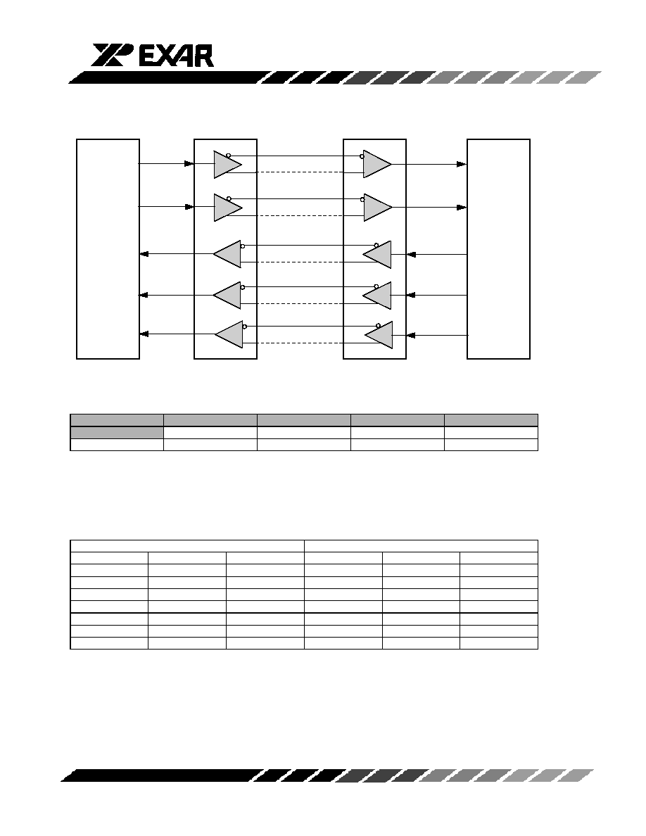
Scenarios 1 & 2
HDLC (R)
HDLC (L)
T4000 (DTE)
T4000 (DCE)
RX1
TX1
RX2
TX2
RX3
TX3
RX2
TX2
RX1
TX1
TXD
SCTE
TXC
RXC
RXD
TXD
SCTE
TXC
RXC
RXD
75
82
90
93
100
97
98
96
95
87
88
79
80
78
77
100
93
84
82
75
78
77
79
80
87
88
96
95
97
98
TXD
SCTE
TXC
RXC
RXD
Options
DTE
Normal
3 Clocks
No Loopback
No Invert
DCE
Echo Mode
2 Clocks
Loopback
Invert
1 Clock (X.21)
Input Pin Settings (Scenarios 1 & 2)
T4000 (DTE)
T4000 (DCE)
Pin Number
Name
State
Pin Number
Name
State
39
DCE/DTE*
0
39
DCE/DTE*
1
42
EC*
1
42
EC*
1
65
2CK/3CK*
0
65
2CK/3CK*
0
22
LP*
1
22
LP*
1
67
CKINV*
1
67
CKINV*
1
68
DTINV*
1
68
DTINV*
1
66
EN_OSC*
1
66
EN_OSC*
1
XRT4000
Rev. 1.00
- 31 -
Scenario 3
HDLC (R)
HDLC (L)
T4000 (DTE)
T4000 (DCE)
RX1
TX1
RX2
TX2
RX3
TX3
RX2
TX2
RX1
TX1
TXD
SCTE
TXC
RXC
RXD
TXD
SCTE
TXC
RXC
RXD
75
82
90
93
100
97
98
96
95
87
88
79
80
78
77
100
93
84
82
75
78
77
79
80
87
88
96
95
97
98
TXD
SCTE
TXC
RXC
RXD
Options
DTE
Normal
3 Clocks
No Loopback
No Invert
DCE
Echo Mode
2 Clocks
Loopback
Invert
1 Clock (X.21)
Input Pin Settings (Scenario 3)
T4000 (DTE)
T4000 (DCE)
Pin Number
Name
State
Pin Number
Name
State
39
DCE/DTE*
0
39
DCE/DTE*
1
42
EC*
1
42
EC*
1
65
2CK/3CK*
0
65
2CK/3CK*
0
22
LP*
0
22
LP*
1
67
CKINV*
1
67
CKINV*
1
68
DTINV*
1
68
DTINV*
1
66
EN_OSC*
1
66
EN_OSC*
1

XRT4000
Rev. 1.00
- 32 -
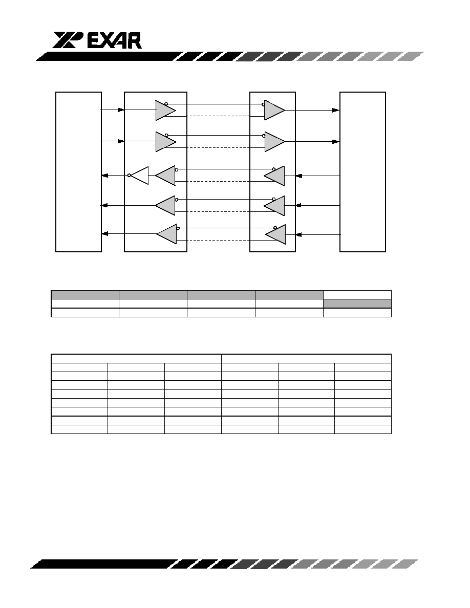
Scenario 4
HDLC (R)
HDLC (L)
T4000 (DTE)
T4000 (DCE)
RX1
TX1
RX2
TX2
RX3
TX3
RX2
TX2
RX1
TX1
TXD
SCTE
TXC
RXC
RXD
TXD
SCTE
TXC
RXC
RXD
75
82
90
93
100
97
98
96
95
87
88
79
80
78
77
100
93
84
82
75
78
77
79
80
87
88
96
95
97
98
TXD
SCTE
TXC
RXC
RXD
Options
DTE
Normal
3 Clocks
No Loopback
No Invert
DCE
Echo Mode
2 Clocks
Loopback
Invert
1 Clock (X.21)
Input Pin Settings (Scenario 4)
T4000 (DTE)
T4000 (DCE)
Pin Number
Name
State
Pin Number
Name
State
39
DCE/DTE*
0
39
DCE/DTE*
1
42
EC*
1
42
EC*
1
65
2CK/3CK*
0
65
2CK/3CK*
0
22
LP*
1
22
LP*
0
67
CKINV*
1
67
CKINV*
1
68
DTINV*
1
68
DTINV*
1
66
EN_OSC*
1
66
EN_OSC*
1
XRT4000
Rev. 1.00
- 33 -
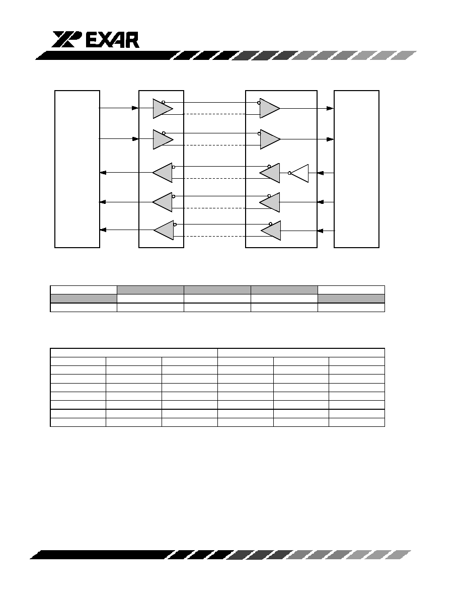
Scenario 5
HDLC (R)
HDLC (L)
T4000 (DTE)
T4000 (DCE)
RX1
TX1
RX2
TX2
RX3
TX3
RX2
TX2
RX1
TX1
TXD
SCTE
TXC
RXC
RXD
TXD
SCTE
TXC
RXC
RXD
75
82
90
93
100
97
98
96
95
87
88
79
80
78
77
100
93
84
82
75
78
77
79
80
87
88
96
95
97
98
TXD
SCTE
TXC
RXC
RXD
Options
DTE
Normal
3 Clocks
No Loopback
No Invert
DCE
Echo Mode
2 Clocks
Loopback
Invert
1 Clock (X.21)
Input Pin Settings (Scenario 5)
T4000 (DTE)
T4000 (DCE)
Pin Number
Name
State
Pin Number
Name
State
39
DCE/DTE*
0
39
DCE/DTE*
1
42
EC*
1
42
EC*
1
65
2CK/3CK*
0
65
2CK/3CK*
0
22
LP*
1
22
LP*
1
67
CKINV*
0
67
CKINV*
1
68
DTINV*
1
68
DTINV*
1
66
EN_OSC*
1
66
EN_OSC*
1
XRT4000
Rev. 1.00
- 34 -
Scenario 6
HDLC (R)
HDLC (L)
T4000 (DTE)
T4000 (DCE)
RX1
TX1
RX2
TX2
RX3
TX3
RX2
TX2
RX1
TX1
TXD
SCTE
TXC
RXC
RXD
TXD
SCTE
TXC
RXC
RXD
75
82
90
93
100
97
98
96
95
87
88
79
80
78
77
100
93
84
82
75
78
77
79
80
87
88
96
95
97
98
TXD
SCTE
TXC
RXC
RXD
Options
DTE
Normal
3 Clocks
No Loopback
No Invert
DCE
Echo Mode
2 Clocks
Loopback
Invert
1 Clock (X.21)
Input Pin Settings (Scenarios 1 & 2)
T4000 (DTE)
T4000 (DCE)
Pin Number
Name
State
Pin Number
Name
State
39
DCE/DTE*
0
39
DCE/DTE*
1
42
EC*
1
42
EC*
1
65
2CK/3CK*
0
65
2CK/3CK*
0
22
LP*
1
22
LP*
1
67
CKINV*
1
67
CKINV*
0
68
DTINV*
1
68
DTINV*
1
66
EN_OSC*
1
66
EN_OSC*
1

XRT4000
Rev. 1.00
- 35 -
Scenario 7
HDLC (R)
HDLC (L)
T4000 (DTE)
T4000 (DCE)
RX1
TX1
RX2
TX2
RX3
TX3
RX2
TX2
RX1
TX1
TXD
SCTE
TXC
RXC
RXD
TXD
SCTE
TXC
RXC
RXD
75
82
90
93
100
97
98
96
95
87
88
79
80
78
77
100
93
84
82
75
78
77
79
80
87
88
96
95
97
98
TXD
SCTE
TXC
RXC
RXD
Options
DTE
Normal
3 Clocks
No Loopback
No Invert
DCE
Echo Mode
2 Clocks
Loopback
Invert
1 Clock (X.21)
Input Pin Settings (Scenarios 7)
T4000 (DTE)
T4000 (DCE)
Pin Number
Name
State
Pin Number
Name
State
39
DCE/DTE*
0
39
DCE/DTE*
1
42
EC*
1
42
EC*
1
65
2CK/3CK*
0
65
2CK/3CK*
0
22
LP*
0
22
LP*
1
67
CKINV*
0
67
CKINV*
1
68
DTINV*
1
68
DTINV*
1
66
EN_OSC*
1
66
EN_OSC*
1

XRT4000
Rev. 1.00
- 36 -
Scenario 8
HDLC (R)
HDLC (L)
T4000 (DTE)
T4000 (DCE)
RX1
TX1
RX2
TX2
RX3
TX3
RX2
TX2
RX1
TX1
TXD
SCTE
TXC
RXC
RXD
TXD
SCTE
TXC
RXC
RXD
75
82
90
93
100
97
98
96
95
87
88
79
80
78
77
100
93
84
82
75
78
77
79
80
87
88
96
95
97
98
TXD
SCTE
TXC
RXC
RXD
Options
DTE
Normal
3 Clocks
No Loopback
No Invert
DCE
Echo Mode
2 Clocks
Loopback
Invert
1 Clock (X.21)
Input Pin Settings (Scenario 8)
T4000 (DTE)
T4000 (DCE)
Pin Number
Name
State
Pin Number
Name
State
39
DCE/DTE*
0
39
DCE/DTE*
1
42
EC*
1
42
EC*
1
65
2CK/3CK*
0
65
2CK/3CK*
0
22
LP*
1
22
LP*
0
67
CKINV*
1
67
CKINV*
0
68
DTINV*
1
68
DTINV*
1
66
EN_OSC*
1
66
EN_OSC*
1
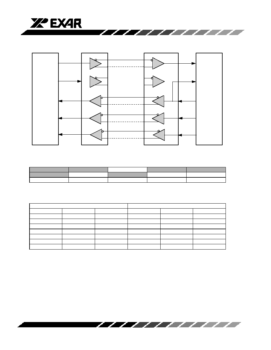
XRT4000
Rev. 1.00
- 37 -
Scenarios 9 & 10
HDLC (R)
HDLC (L)
T4000 (DTE)
T4000 (DCE)
RX1
TX1
RX2
TX2
RX3
TX3
RX2
TX2
RX1
TX1
TXD
SCTE
TXC
RXC
RXD
TXD
SCTE
TXC
RXC
RXD
75
82
90
93
100
97
98
96
95
87
88
79
80
78
77
100
93
84
82
75
78
77
79
80
87
88
96
95
97
98
TXD
TXC
RXC
RXD
Options
DTE
Normal
3 Clocks
No Loopback
No Invert
DCE
Echo Mode
2 Clocks
Loopback
Invert
1 Clock (X.21)
Input Pin Settings (Scenarios 9 & 10)
T4000 (DTE)
T4000 (DCE)
Pin Number
Name
State
Pin Number
Name
State
39
DCE/DTE*
0
39
DCE/DTE*
1
42
EC*
1
42
EC*
1
65
2CK/3CK*
1
65
2CK/3CK*
1
22
LP*
1
22
LP*
1
67
CKINV*
1
67
CKINV*
1
68
DTINV*
1
68
DTINV*
1
66
EN_OSC*
1
66
EN_OSC*
1

XRT4000
Rev. 1.00
- 38 -
Scenario 12
HDLC (R)
HDLC (L)
T4000 (DTE)
T4000 (DCE)
RX1
TX1
RX2
TX2
RX3
TX3
RX2
TX2
RX1
TX1
TXD
SCTE
TXC
RXC
RXD
TXD
SCTE
TXC
RXC
RXD
75
82
90
93
100
97
98
96
95
87
88
79
80
78
77
100
93
84
82
75
78
77
79
80
87
88
96
95
97
98
TXD
TXC
RXC
RXD
Options
DTE
Normal
3 Clocks
No Loopback
No Invert
DCE
Echo Mode
2 Clocks
Loopback
Invert
1 Clock (X.21)
Input Pin Settings (Scenario 12)
T4000 (DTE)
T4000 (DCE)
Pin Number
Name
State
Pin Number
Name
State
39
DCE/DTE*
0
39
DCE/DTE*
1
42
EC*
1
42
EC*
1
65
2CK/3CK*
0
65
2CK/3CK*
1
22
LP*
1
22
LP*
0
67
CKINV*
1
67
CKINV*
1
68
DTINV*
1
68
DTINV*
1
66
EN_OSC*
1
66
EN_OSC*
1

XRT4000
Rev. 1.00
- 39 -
Scenario 13
HDLC (R)
HDLC (L)
T4000 (DTE)
T4000 (DCE)
RX1
TX1
RX2
TX2
RX3
TX3
RX2
TX2
RX1
TX1
TXD
SCTE
TXC
RXC
RXD
TXD
SCTE
TXC
RXC
RXD
75
82
90
93
100
97
98
96
95
87
88
79
80
78
77
100
93
84
82
75
78
77
79
80
87
88
96
95
97
98
TXD
TXC
RXC
RXD
Options
DTE
Normal
3 Clocks
No Loopback
No Invert
DCE
Echo Mode
2 Clocks
Loopback
Invert
1 Clock (X.21)
Input Pin Settings (Scenario 13)
T4000 (DTE)
T4000 (DCE)
Pin Number
Name
State
Pin Number
Name
State
39
DCE/DTE*
0
39
DCE/DTE*
1
42
EC*
1
42
EC*
1
65
2CK/3CK*
1
65
2CK/3CK*
1
22
LP*
1
22
LP*
0
67
CKINV*
0
67
CKINV*
1
68
DTINV*
1
68
DTINV*
1
66
EN_OSC*
1
66
EN_OSC*
1

XRT4000
Rev. 1.00
- 40 -
Scenario 14
HDLC (R)
HDLC (L)
T4000 (DTE)
T4000 (DCE)
RX1
TX1
RX2
TX2
RX3
TX3
RX2
TX2
RX1
TX1
TXD
SCTE
TXC
RXC
RXD
TXD
SCTE
TXC
RXC
RXD
75
82
90
93
100
97
98
96
95
87
88
79
80
78
77
100
93
84
82
75
78
77
79
80
87
88
96
95
97
98
TXD
TXC
RXC
RXD
Options
DTE
Normal
3 Clocks
No Loopback
No Invert
DCE
Echo Mode
2 Clocks
Loopback
Invert
1 Clock (X.21)
Input Pin Settings (Scenario 14)
T4000 (DTE)
T4000 (DCE)
Pin Number
Name
State
Pin Number
Name
State
39
DCE/DTE*
0
39
DCE/DTE*
1
42
EC*
1
42
EC*
1
65
2CK/3CK*
1
65
2CK/3CK*
1
22
LP*
1
22
LP*
1
67
CKINV*
0
67
CKINV*
0
68
DTINV*
1
68
DTINV*
1
66
EN_OSC*
1
66
EN_OSC*
1

XRT4000
Rev. 1.00
- 41 -
Scenario 16
HDLC (R)
HDLC (L)
T4000 (DTE)
T4000 (DCE)
RX1
TX1
RX2
TX2
RX3
TX3
RX2
TX2
RX1
TX1
TXD
SCTE
TXC
RXC
RXD
TXD
SCTE
TXC
RXC
RXD
75
82
90
93
100
97
98
96
95
87
88
79
80
78
77
100
93
84
82
75
78
77
79
80
87
88
96
95
97
98
TXD
TXC
RXC
RXD
Options
DTE
Normal
3 Clocks
No Loopback
No Invert
DCE
Echo Mode
2 Clocks
Loopback
Invert
1 Clock (X.21)
Input Pin Settings (Scenario 16)
T4000 (DTE)
T4000 (DCE)
Pin Number
Name
State
Pin Number
Name
State
39
DCE/DTE*
0
39
DCE/DTE*
1
42
EC*
1
42
EC*
1
65
2CK/3CK*
1
65
2CK/3CK*
1
22
LP*
1
22
LP*
0
67
CKINV*
1
67
CKINV*
0
68
DTINV*
1
68
DTINV*
1
66
EN_OSC*
1
66
EN_OSC*
1

XRT4000
Rev. 1.00
- 42 -
Scenario 17 & 18
HDLC (R)
HDLC (L)
T4000 (DTE)
T4000 (DCE)
RX1
TX1
RX2
TX2
RX3
TX3
RX2
TX2
RX1
TX1
TXD
SCTE
TXC
RXC
RXD
TXD
SCTE
TXC
RXC
RXD
75
82
90
93
100
97
98
96
95
87
88
79
80
78
77
100
93
84
82
75
78
77
79
80
87
88
96
95
97
98
TXD
RXC
RXD
Options
DTE
Normal
3 Clocks
No Loopback
No Invert
DCE
Echo Mode
2 Clocks
Loopback
Invert
1 Clock (X.21)
Input Pin Settings (Scenario 17 & 18)
T4000 (DTE)
T4000 (DCE)
Pin Number
Name
State
Pin Number
Name
State
39
DCE/DTE*
0
39
DCE/DTE*
1
42
EC*
1
42
EC*
1
65
2CK/3CK*
X
65
2CK/3CK*
X
22
LP*
1
22
LP*
1
67
CKINV*
1
67
CKINV*
1
68
DTINV*
1
68
DTINV*
1
66
EN_OSC*
1
66
EN_OSC*
1

XRT4000
Rev. 1.00
- 43 -
Scenario 20
HDLC (R)
HDLC (L)
T4000 (DTE)
T4000 (DCE)
RX1
TX1
RX2
TX2
RX3
TX3
RX2
TX2
RX1
TX1
TXD
SCTE
TXC
RXC
RXD
TXD
SCTE
TXC
RXC
RXD
75
82
90
93
100
97
98
96
95
87
88
79
80
78
77
100
93
84
82
75
78
77
79
80
87
88
96
95
97
98
TXD
RXC
RXD
Options
DTE
Normal
3 Clocks
No Loopback
No Invert
DCE
Echo Mode
2 Clocks
Loopback
Invert
1 Clock (X.21)
Input Pin Settings (Scenario 20)
T4000 (DTE)
T4000 (DCE)
Pin Number
Name
State
Pin Number
Name
State
39
DCE/DTE*
0
39
DCE/DTE*
1
42
EC*
1
42
EC*
1
65
2CK/3CK*
X
65
2CK/3CK*
X
22
LP*
1
22
LP*
0
67
CKINV*
1
67
CKINV*
1
68
DTINV*
1
68
DTINV*
1
66
EN_OSC*
1
66
EN_OSC*
1

XRT4000
Rev. 1.00
- 44 -
Scenario 21
HDLC (R)
HDLC (L)
T4000 (DTE)
T4000 (DCE)
RX1
TX1
RX2
TX2
RX3
TX3
RX2
TX2
RX1
TX1
TXD
SCTE
TXC
RXC
RXD
TXD
SCTE
TXC
RXC
RXD
75
82
90
93
100
97
98
96
95
87
88
79
80
78
77
100
93
84
82
75
78
77
79
80
87
88
96
95
97
98
TXD
RXC
RXD
Options
DTE
Normal
3 Clocks
No Loopback
No Invert
DCE
Echo Mode
2 Clocks
Loopback
Invert
1 Clock (X.21)
Input Pin Settings (Scenario 21)
T4000 (DTE)
T4000 (DCE)
Pin Number
Name
State
Pin Number
Name
State
39
DCE/DTE*
0
39
DCE/DTE*
1
42
EC*
1
42
EC*
1
65
2CK/3CK*
X
65
2CK/3CK*
X
22
LP*
1
22
LP*
1
67
CKINV*
0
67
CKINV*
1
68
DTINV*
1
68
DTINV*
1
66
EN_OSC*
1
66
EN_OSC*
1

XRT4000
Rev. 1.00
- 45 -
Scenario 22
HDLC (R)
HDLC (L)
T4000 (DTE)
T4000 (DCE)
RX1
TX1
RX2
TX2
RX3
TX3
RX2
TX2
RX1
TX1
TXD
SCTE
TXC
RXC
RXD
TXD
SCTE
TXC
RXC
RXD
75
82
90
93
100
97
98
96
95
87
88
79
80
78
77
100
93
84
82
75
78
77
79
80
87
88
96
95
97
98
TXD
RXC
RXD
Options
DTE
Normal
3 Clocks
No Loopback
No Invert
DCE
Echo Mode
2 Clocks
Loopback
Invert
1 Clock (X.21)
Input Pin Settings (Scenario 22)
T4000 (DTE)
T4000 (DCE)
Pin Number
Name
State
Pin Number
Name
State
39
DCE/DTE*
0
39
DCE/DTE*
1
42
EC*
1
42
EC*
1
65
2CK/3CK*
X
65
2CK/3CK*
X
22
LP*
1
22
LP*
1
67
CKINV*
1
67
CKINV*
0
68
DTINV*
1
68
DTINV*
1
66
EN_OSC*
1
66
EN_OSC*
1

XRT4000
Rev. 1.00
- 46 -
Scenario 23
HDLC (R)
HDLC (L)
T4000 (DTE)
T4000 (DCE)
RX1
TX1
RX2
TX2
RX3
TX3
RX2
TX2
RX1
TX1
TXD
SCTE
TXC
RXC
RXD
TXD
SCTE
TXC
RXC
RXD
75
82
90
93
100
97
98
96
95
87
88
79
80
78
77
100
93
84
82
75
78
77
79
80
87
88
96
95
97
98
TXD
RXC
RXD
Options
DTE
Normal
3 Clocks
No Loopback
No Invert
DCE
Echo Mode
2 Clocks
Loopback
Invert
1 Clock (X.21)
Input Pin Settings (Scenario 23)
T4000 (DTE)
T4000 (DCE)
Pin Number
Name
State
Pin Number
Name
State
39
DCE/DTE*
0
39
DCE/DTE*
1
42
EC*
1
42
EC*
1
65
2CK/3CK*
X
65
2CK/3CK*
X
22
LP*
0
22
LP*
1
67
CKINV*
0
67
CKINV*
1
68
DTINV*
1
68
DTINV*
1
66
EN_OSC*
1
66
EN_OSC*
1