 | –≠–ª–µ–∫—Ç—Ä–æ–Ω–Ω—ã–π –∫–æ–º–ø–æ–Ω–µ–Ω—Ç: XRT4500 | –°–∫–∞—á–∞—Ç—å:  PDF PDF  ZIP ZIP |
Document Outline
- General Description
- Table of Contents
- Pin Descriptions
- Figure 1. Supply Current versus Temperature and Supply Voltage, without Load or Signal in EIA-530...
- Figure 2. Supply Current versus Temperature and Supply Voltage, with Load in EIA- 530 (V.11) mode
- Figure 3. RS422 Driver Test Circuit
- Figure 4. RS422 Driver/Receiver AC Test Circuit
- Figure 5. V.35 Driver/Receiver AC Test Circuit (TX1/RX1, TX2/RX2 Only)
- Figure 6. V.10/V.28 Driver Test Circuit
- Figure 7. V.10 (RS-423) V.28 (RS-232) Receiver Test Circuit
- Figure 8. V.11, V.35 Driver Propagation Delays
- Figure 9. V.11, V.35 Receiver Propagation Delays
- Figure 10. V.10 (RS-423) V.28 (RS-232) Driver Propagation Delays
- Figure 11. V.10, V.28 Receiver Propagation Delays
- Table 1: Receiver Specifications
- Table 2: Transmitter Specification
- 1.0 SYSTEM DESCRIPTION
- Table 3: DTE Mode - Control Programming for Driver and Receiver Mode Selection
- Table 4: DCE Mode - Control Programming for Driver and Receiver Mode Selection
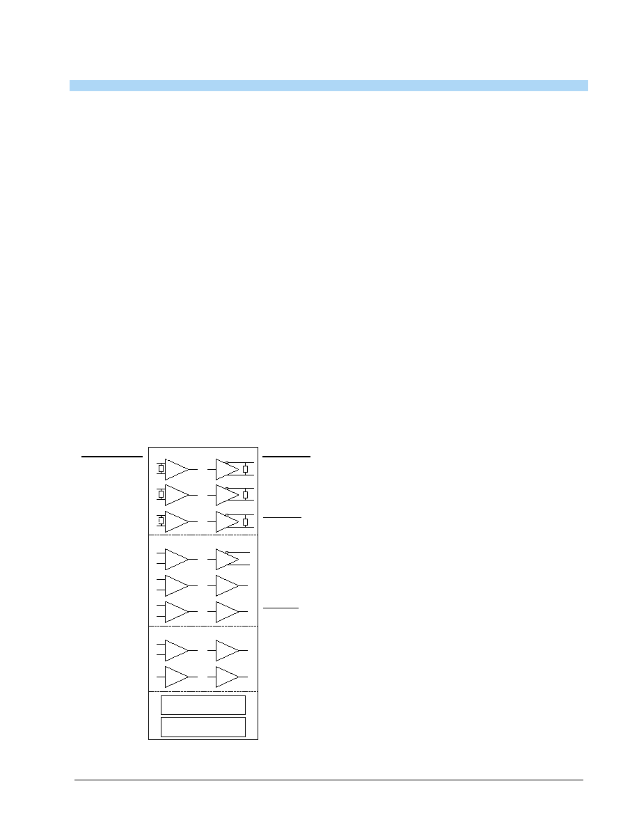
- Figure 12. High-Speed Transceiver Block
- Figure 13. Handshaking/Control Transceiver Block
- Figure 14. Diagnostic Operation indicator Transceiver Block
- Figure 15. Diagram of the XRT4500 Control Block
- Table 5: The Relationship between the settings for the M[2:0] bit-fields and the Corresponding Co...
- Figure 16. A Simple Illustration of the DCE/DTE Interface
- Figure 17. Illustration of both the DTE and DCE Mode XRT4500 operating, when the Loop-Back Mode i...
- Figure 18. Illustration of the Behavior the DTE Mode XRT4500, when it is configured to operate in...
- Figure 19. Illustration of the Behavior of the DCE Mode XRT4500, when it is configured to operate...
- Figure 20. Illustration of a typical ç3-Clock DCE/DTEé Interface
- Figure 21. Illustration of the wave-forms of the signals that are transported across a ç3-Clock D...
- Figure 22. Illustration of a ç2-Clock DTE/DCEé Interface
- Figure 23. The Behavior of the TXC and TXD Signals at the DCE and DTE SCCs, (Data Rate = 1.0Mbps,...
- Figure 24. The Behavior of the TXC and TXD Signals at the DCE and DTE SCCs (Data Rate = 1.544Mbps...
- Figure 25. Illustration of the çEcho-Clocké Feature within the XRT4500
- Figure 26. Illustration of the Wave-forms, across a DCE/DTE Interface, when the Echo-Clock Featur...
- Figure 27. Illustration of the DCE/DTE Interface, with the DCE Mode XRT4500 operating in the ç2- ...
- Figure 28. Illustration of the DCE Mode XRT4500 being configured to invert the TXC signal
- Figure 29. Illustration of the DTE Mode XRT4500 being configured to invert the TXC signal
- Figure 30. Illustration of the DCE Mode XRT4500, which is operating in the ç2-Clocké Mode, and in...
- Figure 31. An Illustration of the Effective Interface between the XRT4500 and the SCC/Microproces...
- Figure 32. An Illustration of the Necessary Glue Logic required to design a feature similar to th...
- Figure 33. Illustration of the Internal Oscillators within the XRT4500
- 2.0 Receiver and Transmitter �Specifications
- 3.0 V.10\V.28 Output Pulse Rise and Fall Time Control
- Figure 34. V.10 Rise/Fall Time as a Function of RSLEW
- Figure 35. V.28 Slew Rate Over ± 3 V Output Range with 3 kW in Parallel with 2500 pF Load as a Fu...
- 4.0 The High-Speed RS232 Mode
- 5.0 Internal Cable Terminations
- 6.0 Operational Scenarios
- 7.0 APPLICATIONS INFORMATION
- Figure 36. Receiver Termination
- Table 6: Receiver Switches
- Figure 37. Transmitter Termination
- Table 7: Transmitter Switches
- Figure 38. Typical V.10 or V.28 Interface (R1 = 10 KW in V.10 and 5 KW in V.28)
- Figure 39. Typical V.11 Interface (Termination Resistor, R1, is Optional.)
- Figure 40. Typical V.35 Interface
- Table 8: MUX1 Connection Table �
- Table 9: MUX2 Connection Table (RX4-RX7, TX4-TX7), Output Versus Input
- Figure 41. Scenario A, MUX2, (DCE/DTE = 0, LP = 0)
- Figure 42. Scenario B, MUX2, (DCE/DTE = 0, LP = 1), Loop Back Not enabled
- Figure 43. Scenario C, MUX2, (DCE/DTE = 1, LP = 0)
- Figure 44. Scenario D, MUX2, (DCE/DTE = 1, LP = 1), Loop Back Not enabled
- Figure 45. Serial Interface Signals and Connector Pin-Out
- Figure 46. Serial Interface Connector Drawings
- Figure 47. EIA-530 Connection Diagram for XRT4500
- Figure 48. RS-232 Connection Diagram for XRT4500
Exar
Corporation 48720 Kato Road, Fremont CA, 94538
∑
(510) 668-7000
∑
FAX (510) 668-7017
∑
www.exar.com
·Á
·Á
·Á
·Á
XRT4500
MULTIPROTOCOL SERIAL NETWORK INTERFACE IC
SEPTEMBER 2002
REV. 1.0.7
GENERAL DESCRIPTION
The XRT4500 is a fully integrated multiprotocol serial
interface. It supports all of the popular serial commu-
nication interface standards such as ITU-T V.35, ITU-
T V.36, EIA530A, RS232 (ITU-T V.28), ITU-T X.21
and RS449. It can easily be interfaced with most
common types of Serial Communications Controllers
(SCCs). This device contains eight receivers and
eight transmitters, in groups of six or seven. It is a
complete solution containing all of the required
source and load termination resistors in one 80-pin
TQFP package. The XRT4500 operates at higher
speeds (20MHz for V.35 and 256kbps for V.28).
The XRT4500 can be configured to operate in one of
the seven interface standards in either DTE, or DCE
modes of operation and power down mode. It fully
supports echoed clock as well as clock and data in-
version. Loopbacks are supported in DTE and DCE
modes of operation. This feature eliminates the need
for external circuitry for loopback implementation.
Control signals such as RI, RL, DCD, DTR, DSR are
protected against glitches by internal filters. These fil-
ters can be turned off. The XRT4500 provides an in-
ternal oscillator (clock signal) which can be used to
conduct standalone diagnostics of DTE equipment.
B
LOCK
D
IAGRAM
FEATURES
∑ Pin Programmable Multiprotocol Serial Interface
∑ V.35, V.36, EIA-530 A, RS232 (V.28), V.10, V.11, X.21
and RS449 Communication Interface Standards
∑ V.28, V.10, V.11 and V.35 Electrical Interfaces are
`CTR2' Compliant
∑ Contains On-Chip Source and Load Termination
Resistors
∑ Contains Eight Receivers and Eight Transmitters
with Switchable DTE and DCE Modes
∑ Glitch Filters on the Control Signals (Selectable)
∑ +5V Single Power Supply with internal DC-DC
Converter
∑ Full Support of Loopbacks, Data & Clock Inversion,
and Echoed Clock in DTE and DCE Modes
∑ Full Support of Most Popular Types of HDLC Control-
lers (Single, Double, and Triple Clocks supported)
∑ High-speed V.28 Driver: 256KHz
∑ Internal Oscillator for Standalone DTE Loopback
Testing
∑ Control Signals Can Be Registered and Non-regis-
tered
∑ Control Signals Can Be Tri-stated for Bus-based
Designs
∑ "Cable Safe" Operation Supported
∑ ESD Protection Over ± 1KV Range
∑ TTL Level Digital Inputs
∑ TTL/CMOS Digital Outputs
APPLICATIONS
∑ Data Service Units (DSU)
∑ Channel Service Units (CSU)
∑ Routers
∑ Bridges
∑ Access Equipment
TX2
TX1
RX3
RX2
RX1
TX4
TX3
RX4
RX5
TX5
TX6
RX6
TX7
RX8
RX7
V.10, V.11, V.35, V.28
Electrical Interfaces
Signals
TXD, RXD
High Speed Data
and Clock
V.10, V.11, V.35, V.28
V.10, V.11, V.35, V.28
SCTE Signals:
DCE Transmitter,
DTE Receiver
RTS, CTS
DTR, DSR
LL, RL, RI (TM)
LL, RL, RI (TM)
Mode and Configuration
Control
Switching Regulator
DC-DC Converter
V.10, V.11, ---- , V.28
V.10, V.11, ---- , V.28
V.10, V.11, ---- , V.28
V.10, ---- , ---- , V.28
V.10, ---- , ---- , V.28
High Speed Transceiver
TXC, RXC
High Speed Data
and Clock
DCD Signals:
DCE Transmitter,
DTE Receiver
Diagnostic Transceivers
TX8
Handshaking/Control Transceivers

·Á
·Á
·Á
·Á
XRT4500
MULTIPROTOCOL SERIAL NETWORK INTERFACE IC
REV. 1.0.7
2
B
LOCK
D
IAGRAM
Digital MUX 1
47µ
F
L o w E S R
-6V
2 6
- 6 V
S w i t c h i n g R e g u l a t o r
4 1
5 6
5 2
4 2
4 3
+ 1 2 V
C h a r g e P u m p
2 1
2 2
2 . 2
µ
F
V
S S
V s e n s e V
S S
_ T 1 2 3
S R _ O U T
I s e n s e
G N D _ R E G
C P P
C P M
1 N 5 8 1 9
4 7
µ
H
0 . 5
-
+
1 6
D e c o d e r
L a t c h
4
5
6
4 4
XRT4500
MODE & CONFIGURATION
CONTROL LOGIC
3 2 - 6 4 K H z
S L E W R A T E
C O N T R O L
4 5
3 9
R
slew
M 0
M 1
M 2
C L K F S
S L E W _ C N T L
M o d e S e l e c t
Echo Clock 34
2 or 3 Clock Select 50
Invert Clock 54
Register 24
Invert Data 55
L o o p b a c k
R e g i s t e r M o d e
Clock Input
M o d e C o n t r o l
4 9
R E G _ C L K
R E G
2 C K / 3 C K
L P
C L K I N V
D T I N V
E C
D E C / D T E
5 1
V D D _ R E G
V D D
R X 1 B
R X 1 , 2 , 3
R X 1 D
R X 1 A
2
7 8
7 9
R X 2 D
R X 1
1
R X 8 D
R X 8 I
2 5
2 3
R X 8
Filter
G N D
R X 1 , 2 , 3
3
R X 5 B
R X 5 D
R X 5 A
3 6
3 3
3 5
R X 5
Filter
R X 2 B
R X 2 A
T
7 7
7 4
7 6
R X 2
R X 3 D
7 3
R X 3
R X 6 7 D
3 2
R X 4 , 5 , 6 , 7
R X 7
R X 6
Filter
Filter
7 5
E N _ F L T R
T X 1 , 2 , 3
5 8
V D D _ T 1 2 3
6 7
T X 2 D
T
6 4
T X 2 A
6 6 C M _ T X 2
T X 2 B
6 5
6 8
T X 3 D
T
7 0
T R 3 A
6 9 C M _ T R 3
T R 3 B
7 1
8
T X 4 D
1 1
T X 4 A
T X 4 B
1 0
T X 2
T X 4
T X 3
1 5
T X 5 D
1 2
T X 5 A
T X 5 B
1 3
2 7
T R 7
T X 7
T X 5
G N D _ T 1 2
6 0
T X 1 D
T
6 3
T X 1 A
6 1 C M _ T X 1
T X 1 B
6 2
T X 1
T X 1 , 2
5 9
7 2 G N D
9 V D D
T X 4 , 5 , 6 , 7 , 8
2 9
T R 6 A
T R 6 B
3 0
T X 6
M U X
2 8 TX76D
V . 1 1 ( R X 1 , 2 , 3 ) T e r m i n a t i o n 8 0
E N _ T E R M
Digital MUX 2
4 6
Glitch Filter
4 8
E N _ O U T
M U X
E _ 2 3 2 H
O S C E N
5 3
T X 1 , 2 , 3
5 7 G N D
R X 4 , 5 , 6 , 7 , 8
7
V
S S
1 7
T X 8 D
1 9 T X 8 O
G N D
1 4
T X 4 , 5 , 6 , 7 , 8
T X 8
T
H i g h S p e e d R S 2 3 2 E n a b l e
2 0
V D D
R X 4 B
R X 4 D
R X 4 A
3 7
4 0
3 8
R X 4
Filter
V
P P
+
1 0
µ
F
0 . 1
0 . 1
0 . 1
V D D 4 7
L A T C H
Mode Control
MUX Control
1 8
3 1
5 0 0 K Hz
C L O C K
+
-
XRT4500
·Á
·Á
·Á
·Á
MULTIPROTOCOL SERIAL NETWORK INTERFACE IC
REV. 1.0.7
3
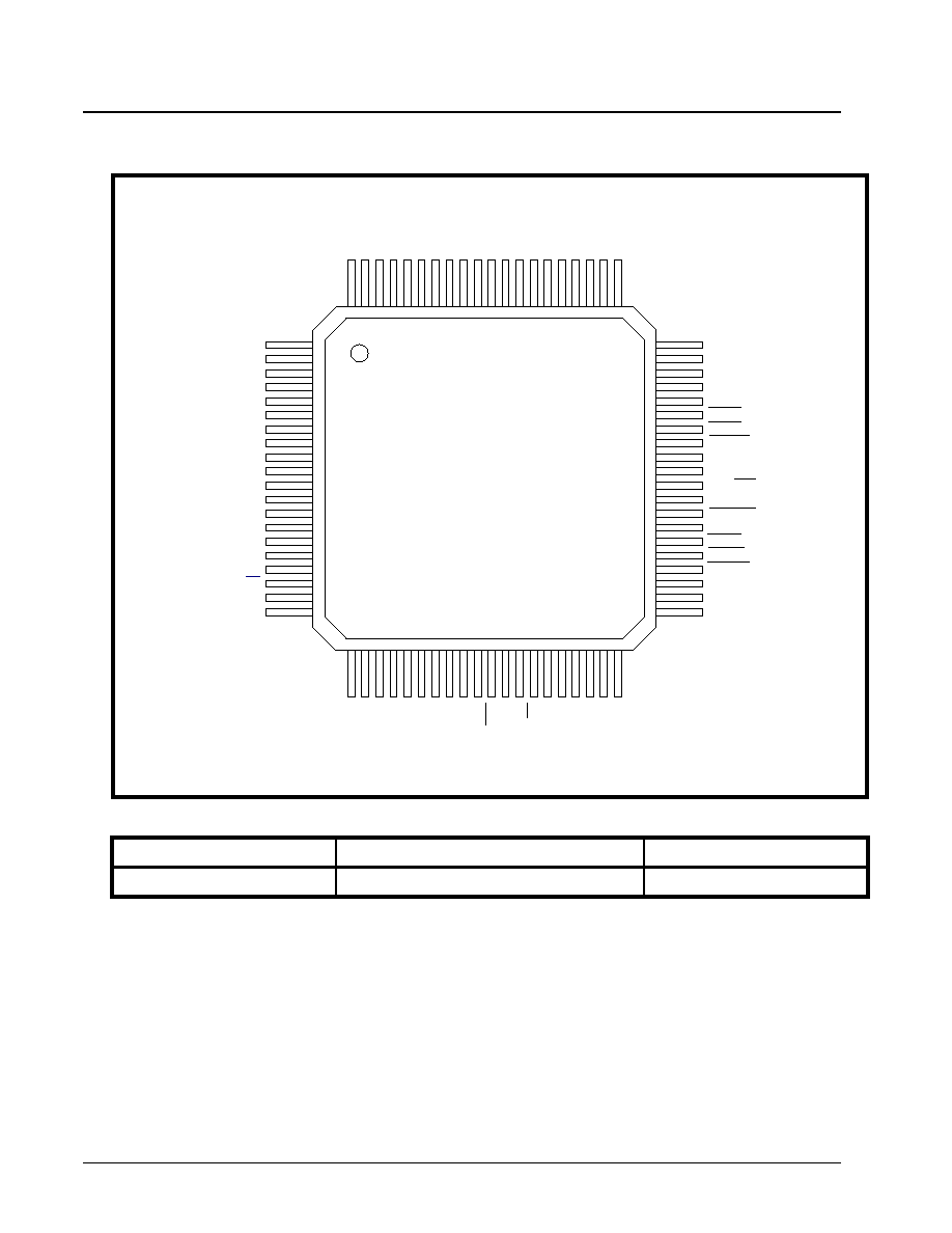
P
IN
O
UT
OF
THE
D
EVICE
O
RDERING
I
NFORMATION
P
ART
N
UMBER
P
ACKAGE
O
PERATING
T
EMPERATURE
R
ANGE
XRT4500CV
80 Pin TQFP
0
∞
C to +70
∞
C
CPP
CPM
RX8D
REG
RX8I
VSS
TR7
TX76D
TR6A
TR6B
DCE/DTE
RX67D
RX5D
EC
RX5B
RX5A
RX4A
RX4B
SLEW_CNTL
RX4D
XRT4500
80 Lead TQFP
1
2
3
4
5
6
7
8
9
1 0
1 1
1 2
1 3
1 4
1 5
1 6
1 7
1 8
1 9
2 0
6 0
5 9
5 8
5 7
5 6
5 5
5 4
5 3
5 2
5 1
5 0
4 9
4 8
4 7
4 6
4 5
4 4
4 3
4 2
4 1
21
22
23
24
25
26
27
28
29
30
31
32
33
34
35
36
37
38
39
40
80
79
78
77
76
75
74
73
72
71
70
69
68
67
66
65
64
63
62
61
EN_TERM
RX1B
RX1A
RX2A
RX2B
EN_FLTR
RX2D
RX3D
GND
TR3B
TR3A
CM_TR3
TX3D
TX2D
CM_TX2
TX2B
TX2A
TX1A
TX1B
CM_TX1
V D D
T X 8 O
L P
T X 8 D
V P P
T X 5 D
G N D
T X 5 B
T X 5 A
T X 4 A
T X 4 B
V D D
T X 4 D
B I A S
M 2
M 1
M 0
G N D
V D D
R X 1 D
T X 1 D
G N D
V D D
G N D
V S S
D T I N V
C K I N V
O S C E N
S R _ O U T
V D D
2 C K / 3 C K
R E G _ C L K
E N _ O U T
V D D
E - 2 3 2
C L K F S
L A T C H
G N D
I _ S E N S E
V _ S E N S E

·Á
·Á
·Á
·Á
XRT4500
MULTIPROTOCOL SERIAL NETWORK INTERFACE IC
REV. 1.0.7
I
TABLE OF CONTENTS
GENERAL DESCRIPTION................................................................................................. 1
Block Diagram........................................................................................................................................... 1
F
EATURES
...................................................................................................................................... 1
A
PPLICATIONS
................................................................................................................................ 1
Block Diagram........................................................................................................................................... 2
Pin Out of the Device ................................................................................................................................ 3
Ordering Information ................................................................................................................................. 3
T
ABLE
OF
C
ONTENTS
............................................................................................................ I
PIN DESCRIPTIONS .......................................................................................................... 4
E
LECTRICAL
C
HARACTERISTICS
.................................................................................................... 26
TA = 25∞C, VDD = 5V, VSS = -6V, VPP = 12V, Maximum Operating Frequency Unless Otherwise Specified
28
Power Supply Consumption.................................................................................................................... 29
F
IGURE
1. S
UPPLY
C
URRENT
VERSUS
T
EMPERATURE
AND
S
UPPLY
V
OLTAGE
,
WITHOUT
L
OAD
OR
S
IGNAL
IN
EIA-530 (V.11)
MODE
......................................................................................................................................................... 29
F
IGURE
2. S
UPPLY
C
URRENT
VERSUS
T
EMPERATURE
AND
S
UPPLY
V
OLTAGE
,
WITH
L
OAD
IN
EIA-530 (V.11)
MODE
... 30
F
IGURE
3. RS422 D
RIVER
T
EST
C
IRCUIT
................................................................................................................. 33
F
IGURE
4. RS422 D
RIVER
/R
ECEIVER
AC T
EST
C
IRCUIT
........................................................................................... 33
F
IGURE
5. V.35 D
RIVER
/R
ECEIVER
AC T
EST
C
IRCUIT
(TX1/RX1, TX2/RX2 O
NLY
) .................................................. 34
F
IGURE
6. V.10/V.28 D
RIVER
T
EST
C
IRCUIT
............................................................................................................ 34
F
IGURE
7. V.10 (RS-423) V.28 (RS-232) R
ECEIVER
T
EST
C
IRCUIT
......................................................................... 34
F
IGURE
8. V.11, V.35 D
RIVER
P
ROPAGATION
D
ELAYS
.............................................................................................. 34
F
IGURE
9. V.11, V.35 R
ECEIVER
P
ROPAGATION
D
ELAYS
.......................................................................................... 34
F
IGURE
10. V.10 (RS-423) V.28 (RS-232) D
RIVER
P
ROPAGATION
D
ELAYS
............................................................. 35
F
IGURE
11. V.10, V.28 R
ECEIVER
P
ROPAGATION
D
ELAYS
........................................................................................ 35
T
ABLE
1: R
ECEIVER
S
PECIFICATIONS
....................................................................................................................... 35
T
ABLE
2: T
RANSMITTER
S
PECIFICATION
.................................................................................................................... 36
1.0 SYSTEM DESCRIPTION ..................................................................................................................... 37
1.1 THE DIFFERENCE BETWEEN AN ELECTRICAL INTERFACE AND A COMMUNICATIONS INTERFACE 37
T
ABLE
3: DTE M
ODE
- C
ONTROL
P
ROGRAMMING
FOR
D
RIVER
AND
R
ECEIVER
M
ODE
S
ELECTION
.............................. 38
T
ABLE
4: DCE M
ODE
- C
ONTROL
P
ROGRAMMING
FOR
D
RIVER
AND
R
ECEIVER
M
ODE
S
ELECTION
.............................. 38
1.2 THE SYSTEM ARCHITECTURE .................................................................................................................... 39
1.2.1 THE "HIGH -SPEED TRANSCEIVER" BLOCK ......................................................................................................... 40
F
IGURE
12. H
IGH
-S
PEED
T
RANSCEIVER
B
LOCK
........................................................................................................ 40
1.2.2 THE "HANDSHAKING/CONTROL SIGNAL TRANSCEIVER" BLOCK .................................................................... 41
F
IGURE
13. H
ANDSHAKING
/C
ONTROL
T
RANSCEIVER
B
LOCK
...................................................................................... 41
1.2.3 THE "DIAGNOSTIC OPERATION INDICATOR TRANSCEIVER" BLOCK............................................................... 42
F
IGURE
14. D
IAGNOSTIC
O
PERATION
INDICATOR
T
RANSCEIVER
B
LOCK
..................................................................... 42
1.3 THE CONTROL BLOCK ................................................................................................................................. 43
F
IGURE
15. D
IAGRAM
OF
THE
XRT4500 C
ONTROL
B
LOCK
........................................................................................ 43
1.3.1 M[2:0] - THE (COMMUNICATION INTERFACE) MODE CONTROL SELECT PINS. ............................................... 44
T
ABLE
5: T
HE
R
ELATIONSHIP
BETWEEN
THE
SETTINGS
FOR
THE
M[2:0]
BIT
-
FIELDS
AND
THE
C
ORRESPONDING
C
OMMUNICA
-
TION
I
NTERFACE
THAT
IS
SUPPORTED
.......................................................................................................... 44
1.3.2 DCE/DTE - THE DCE/DTE MODE SELECT PIN ........................................................................................................ 45
F
IGURE
16. A S
IMPLE
I
LLUSTRATION
OF
THE
DCE/DTE I
NTERFACE
.......................................................................... 45
1.3.3 THE LP - LOOP-BACK ENABLE/DISABLE SELECT PIN ........................................................................................ 46
F
IGURE
17. I
LLUSTRATION
OF
BOTH
THE
DTE
AND
DCE M
ODE
XRT4500
OPERATING
,
WHEN
THE
L
OOP
-B
ACK
M
ODE
IS
DIS
-
ABLED
........................................................................................................................................................ 46
F
IGURE
18. I
LLUSTRATION
OF
THE
B
EHAVIOR
THE
DTE M
ODE
XRT4500,
WHEN
IT
IS
CONFIGURED
TO
OPERATE
IN
THE
L
OOP
-
B
ACK
M
ODE
............................................................................................................................................... 47
F
IGURE
19. I
LLUSTRATION
OF
THE
B
EHAVIOR
OF
THE
DCE M
ODE
XRT4500,
WHEN
IT
IS
CONFIGURED
TO
OPERATE
IN
THE
L
OOP
-
BACK
M
ODE
...................................................................................................................................... 48
1.3.4 THE EC* (ECHO CLOCK MODE - ENABLE/DISABLE SELECT INPUT PIN) .......................................................... 49
F
IGURE
20. I
LLUSTRATION
OF
A
TYPICAL
"3-C
LOCK
DCE/DTE" I
NTERFACE
............................................................... 49
F
IGURE
21. I
LLUSTRATION
OF
THE
WAVE
-
FORMS
OF
THE
SIGNALS
THAT
ARE
TRANSPORTED
ACROSS
A
"3-C
LOCK
DTE/DCE"
I
NTERFACE
................................................................................................................................................. 50

XRT4500
·Á
·Á
·Á
·Á
MULTIPROTOCOL SERIAL NETWORK INTERFACE IC
REV. 1.0.7
II
F
IGURE
22. I
LLUSTRATION
OF
A
"2-C
LOCK
DTE/DCE" I
NTERFACE
............................................................................ 51
F
IGURE
23. T
HE
B
EHAVIOR
OF
THE
TXC
AND
TXD S
IGNALS
AT
THE
DCE
AND
DTE SCC
S
, (D
ATA
R
ATE
= 1.0M
BPS
, "DCE-
TO
-DTE"
PROPAGATION
DELAY
= 160
NS
, "DTE-
TO
-DCE"
PROPAGATION
DELAY
= 160
NS
)............................ 52
F
IGURE
24. T
HE
B
EHAVIOR
OF
THE
TXC
AND
TXD S
IGNALS
AT
THE
DCE
AND
DTE SCC
S
(D
ATA
R
ATE
= 1.544M
BPS
, DCE-
TO
-DTE P
ROPAGATION
D
ELAY
= 160
NS
, DTE-
TO
-DCE P
ROPAGATION
D
ELAY
= 160
NS
) ............................. 52
F
IGURE
25. I
LLUSTRATION
OF
THE
"E
CHO
-C
LOCK
" F
EATURE
WITHIN
THE
XRT4500 ................................................... 53
F
IGURE
26. I
LLUSTRATION
OF
THE
W
AVE
-
FORMS
,
ACROSS
A
DCE/DTE I
NTERFACE
,
WHEN
THE
E
CHO
-C
LOCK
F
EATURE
(
WITHIN
THE
XRT4500)
IS
USED
AS
DEPICTED
IN
F
IGURE
25........................................................................ 54
1.3.5 THE "2CK/3CK" (2-CLOCK/3-CLOCK MODE - ENABLE/DISABLE SELECT INPUT PIN) ..................................... 54
F
IGURE
27. I
LLUSTRATION
OF
THE
DCE/DTE I
NTERFACE
,
WITH
THE
DCE M
ODE
XRT4500
OPERATING
IN
THE
"2-C
LOCK
"
M
ODE
........................................................................................................................................................ 55
1.3.6 THE "CLOCK INVERSION" (CK_INV) FEATURE ..................................................................................................... 55
F
IGURE
28. I
LLUSTRATION
OF
THE
DCE M
ODE
XRT4500
BEING
CONFIGURED
TO
INVERT
THE
TXC
SIGNAL
................ 56
F
IGURE
29. I
LLUSTRATION
OF
THE
DTE M
ODE
XRT4500
BEING
CONFIGURED
TO
INVERT
THE
TXC
SIGNAL
................ 56
F
IGURE
30. I
LLUSTRATION
OF
THE
DCE M
ODE
XRT4500,
WHICH
IS
OPERATING
IN
THE
"2-C
LOCK
" M
ODE
,
AND
INVERTING
THE
"TXC"
SIGNAL
..................................................................................................................................... 57
1.3.7 THE LATCH MODE OF OPERATION ........................................................................................................................ 58
1.3.8 THE REGISTERED MODE OF OPERATION ............................................................................................................. 58
F
IGURE
31. A
N
I
LLUSTRATION
OF
THE
E
FFECTIVE
I
NTERFACE
BETWEEN
THE
XRT4500
AND
THE
SCC/M
ICROPROCESSOR
WHEN
THE
"R
EGISTERED
" M
ODE
IS
ENABLED
............................................................................................... 58
F
IGURE
32. A
N
I
LLUSTRATION
OF
THE
N
ECESSARY
G
LUE
L
OGIC
REQUIRED
TO
DESIGN
A
FEATURE
SIMILAR
TO
THAT
OFFERED
BY
THE
"R
EGISTERED
" M
ODE
,
WHEN
USING
A
DIFFERENT
M
ULTI
-
PROTOCOL
S
ERIAL
N
ETWORK
I
NTERFACE
IC 59
1.3.9 THE INTERNAL OSCILLATOR .................................................................................................................................. 59
F
IGURE
33. I
LLUSTRATION
OF
THE
I
NTERNAL
O
SCILLATORS
WITHIN
THE
XRT4500..................................................... 60
1.3.10 GLITCH FILTERS...................................................................................................................................................... 60
1.3.11 DATA INVERSION .................................................................................................................................................... 60
1.3.12 DATA INTERLUDE ................................................................................................................................................... 60
2.0 RECEIVER AND TRANSMITTER SPECIFICATIONS .........................................................................60
3.0 V.10\V.28 OUTPUT PULSE RISE AND FALL TIME CONTROL .........................................................60
F
IGURE
34. V.10 R
ISE
/F
ALL
T
IME
AS
A
F
UNCTION
OF
RSLEW ................................................................................. 61
F
IGURE
35. V.28 S
LEW
R
ATE
O
VER
± 3 V O
UTPUT
R
ANGE
WITH
3
K
W
IN
P
ARALLEL
WITH
2500
P
F L
OAD
AS
A
F
UNCTION
OF
RSLEW................................................................................................................................................ 61
4.0 THE HIGH-SPEED RS232 MODE ........................................................................................................61
5.0 INTERNAL CABLE TERMINATIONS ..................................................................................................62
6.0 OPERATIONAL SCENARIOS ..............................................................................................................62
7.0 APPLICATIONS INFORMATION .........................................................................................................62
F
IGURE
36. R
ECEIVER
T
ERMINATION
........................................................................................................................ 63
T
ABLE
6: R
ECEIVER
S
WITCHES
................................................................................................................................ 63
F
IGURE
37. T
RANSMITTER
T
ERMINATION
.................................................................................................................. 64
T
ABLE
7: T
RANSMITTER
S
WITCHES
........................................................................................................................... 64
F
IGURE
38. T
YPICAL
V.10
OR
V.28 I
NTERFACE
(R1 = 10 KW
IN
V.10
AND
5 KW
IN
V.28) ........................................ 64
F
IGURE
39. T
YPICAL
V.11 I
NTERFACE
(T
ERMINATION
R
ESISTOR
, R1,
IS
O
PTIONAL
.).................................................. 64
F
IGURE
40. T
YPICAL
V.35 I
NTERFACE
...................................................................................................................... 65
T
ABLE
8: MUX1 C
ONNECTION
T
ABLE
....................................................................................................................... 65
T
ABLE
9: MUX2 C
ONNECTION
T
ABLE
(RX4-RX7, TX4-TX7), O
UTPUT
V
ERSUS
I
NPUT
.............................................. 67
F
IGURE
41. S
CENARIO
A, MUX2, (DCE/DTE = 0, LP = 0)....................................................................................... 68
F
IGURE
42. S
CENARIO
B, MUX2, (DCE/DTE = 0, LP = 1), L
OOP
B
ACK
N
OT
ENABLED
............................................. 69
F
IGURE
43. S
CENARIO
C, MUX2, (DCE/DTE = 1, LP = 0)....................................................................................... 70
F
IGURE
44. S
CENARIO
D, MUX2, (DCE/DTE = 1, LP = 1), L
OOP
B
ACK
N
OT
ENABLED
............................................. 71
F
IGURE
45. S
ERIAL
I
NTERFACE
S
IGNALS
AND
C
ONNECTOR
P
IN
-O
UT
......................................................................... 72
F
IGURE
46. S
ERIAL
I
NTERFACE
C
ONNECTOR
D
RAWINGS
........................................................................................... 73
F
IGURE
47. EIA-530 C
ONNECTION
D
IAGRAM
FOR
XRT4500 .................................................................................... 74
F
IGURE
48. RS-232 C
ONNECTION
D
IAGRAM
FOR
XRT4500 ..................................................................................... 75
Scenarios 1 & 2 Normal: `3-clock' DCE/DTE Interface Operation ...........................................................76
Input Pin Settings ....................................................................................................................................76
Scenario 3 &2 DTE Loop-Back Mode......................................................................................................77
Input Pin Settings ....................................................................................................................................77
Scenario 4 ...............................................................................................................................................78
Comments: DCE Loop-Back Mode .........................................................................................................78

·Á
·Á
·Á
·Á
XRT4500
MULTIPROTOCOL SERIAL NETWORK INTERFACE IC
REV. 1.0.7
III
Input Pin Settings .................................................................................................................................... 78
Scenario 5 & 2......................................................................................................................................... 79
Comments: TXC Clock Inversion in DTE Mode ...................................................................................... 79
Input Pin Settings .................................................................................................................................... 79
Scenario 6 ............................................................................................................................................... 80
Comments: TXC Clock Inversion in DCE Mode...................................................................................... 80
Input Pin Settings .................................................................................................................................... 80
Scenario 7 & 2......................................................................................................................................... 81
Input Pin Settings .................................................................................................................................... 81
Scenario 8 ............................................................................................................................................... 82
Input Pin Settings .................................................................................................................................... 82
Scenario 9 & 10....................................................................................................................................... 83
Comments: 2 Clock Mode Operation Within the `DCE Mode'. This feature is Useful For Applications .. 83
That Interface to a Device Which Does Not Supply `SCTE' Clock Signal............................................... 83
Input Pin Settings .................................................................................................................................... 83
Scenario 12 ............................................................................................................................................. 84
Input Pin Settings .................................................................................................................................... 84
Scenario 13 & 10..................................................................................................................................... 85
Input Pin Settings .................................................................................................................................... 85
Scenario 14 ............................................................................................................................................. 86
Comments: TXC Clock Inversion and 2 Clock Mode Operation Within The DCE Mode. This Scenario Can
be Used to Resolve the 2 Clock Propagation Delay Timing Violation Issue. .......................................... 86
Input Pin Settings .................................................................................................................................... 86
Scenario 16 ............................................................................................................................................. 87
Input Pin Settings .................................................................................................................................... 87
Scenario 17 & 18..................................................................................................................................... 88
Comments: X:21 Mode Operation........................................................................................................... 88
Input Pin Settings (1 clock mode) ........................................................................................................... 88
Scenario 20 ............................................................................................................................................. 89
Input Pin Settings (1 clock mode) ........................................................................................................... 89
Scenario 21 ............................................................................................................................................. 90
Input Pin Settings (1 clock mode) ........................................................................................................... 90
Scenario 22 ............................................................................................................................................. 91
Input Pin Settings (1 clock mode) ........................................................................................................... 91
Scenario 23 ............................................................................................................................................. 92
Input Pin Settings (1 clock mode) ........................................................................................................... 92
Scenario 48 ............................................................................................................................................. 93
Input Pin Settings (1 clock mode) ........................................................................................................... 93
R
EVISIONS
................................................................................................................................... 96
XRT4500
·Á
·Á
·Á
·Á
MULTIPROTOCOL SERIAL NETWORK INTERFACE IC
REV. 1.0.7
4
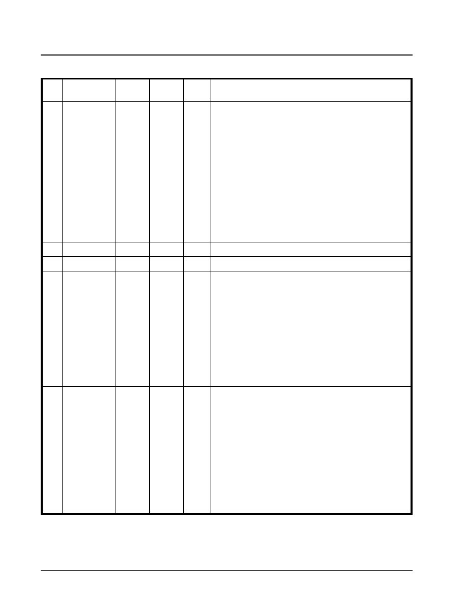
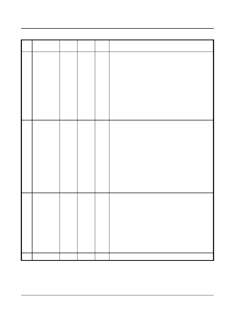
PIN DESCRIPTIONS
PIN
#
Signal
DTE
MODE
DCE
MODE
TYPE
FUNCTION
1
RX1D
D_RXD
D_TXD
O
Receiver 1 Digital Output ≠ Digital Data Output to terminal
equipment
This output pin is the digital (TTL/CMOS level) representation of
the line signal that has been received via the RX1A (pin 78) and
RX1B (pin 79) input pins.
The exact role that this pin plays depends upon whether the
XRT4500 is operating in the DCE or DTE Mode.
DCE Mode ≠ TXD Digital Output Signal
This output pin functions as the TXD Digital Output signal (which
should be input to the Terminal Equipment).
DTE Mode ≠ RXD Digital Output Signal
This output pin functions as the RXD Digital Output signal (which
should be input to the Terminal Equipment).
2
VDD
Analog VDD for Receiver 1, 2, 3
3
GND
I
Analog GND for Receiver 1, 2, 3 and Transmitter 3
4
M0
I
Mode Control ≠ Mode Select Input 0
This input pin, along with M1 and M2 are used to configure the
XRT4500 to operate in the desired "Communication Interface"
Mode. Table 3 and Table 4 present the relationship between
the states of the M2, M1 and M0 input pins and the correspond-
ing communication interface modes selected.
This input pin (along with M1 and M2) is internally latched into
the XRT4500, upon the rising edge of the "LATCH" signal. At this
point, changes in this input pin will not effect the "internally
latched" state of this pin.
This input pin contains an Internal 20K
pull-up to VDD.
5
M1
I
Mode Control ≠ Mode Select Input 1
This input pin, along with M0 and M2 are used to configure the
XRT4500 to operate in the desired "Communication Interface"
Mode. Table 3 and Table 4 present the relationship between the
states of the M2, M1 and M0 input pins and the corresponding
communication interface modes selected.
This input pin (along with M0 and M2) is internally latched into the
XRT4500 device, upon the rising edge of the "LATCH" signal. At
this point, changes in this input pin will not effect the "internally
latched" state of this pin.
This input pin contains an Internal 20K
pull-up to VDD.
·Á
·Á
·Á
·Á
XRT4500
MULTIPROTOCOL SERIAL NETWORK INTERFACE IC
REV. 1.0.7
5
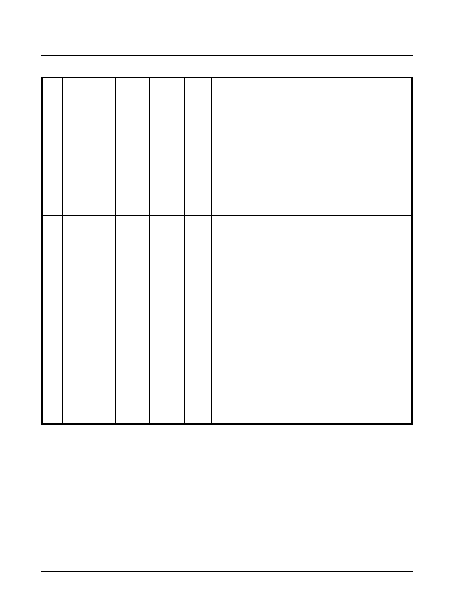
PIN DESCRIPTIONS (CONT.)
PIN
#
Signal
DTE
MODE
DCE
MODE
TYPE FUNCTION
6
M2
I
Mode Control ≠ Mode Select Input 2
This input pin, along with M0 and M1 are used to configure the
XRT4500 to operate in the desired "Communication Interface"
Mode. Table 3 and Table 4 present the relationship between
the states of the M2, M1 and M0 input pins and the correspond-
ing communication interface modes selected.
This input pin (along with M0 and M1) is internally latched into
the XRT4500 device, upon the rising edge of the "LATCH" sig-
nal. At this point, changes in this input pin will not effect the
"internally latched" state of this pin.
This input pin contains an Internal 20K
pull-up to VDD.
7
VSS
-6V Power: This supply voltage is internally generated by the
Switching Regulator Circuit within the XRT4500. The -6V is used
by TX 4, 5, 6, 7, 8.
8
TX4D
D_RTS
D_CTS
I
Transmitter 4 ≠ Digital Data Input from Terminal Equipment
The XRT4500 accepts binary TTL Level data stream, via this
input pin, converts it into either a V.10, V.11 or V.28 format and
outputs it via the TX4A and TX4B output pins.
The exact role that this pin plays depends upon whether the
XRT4500 is operating in the DCE or DTE Mode.
DCE Mode ≠ CTS (Clear to Send) Input
If the XRT4500 is operating in the DCE Mode, then this input pin
should be tied to the CTS Output pin of the Terminal Equipment.
DTE Mode ≠ RTS (Request to Send) Input
If the XRT4500 is operating in the DTE Mode, then this input pin
should be tied to the RTS output pin of the Terminal Equipment.
9
VDD
Analog VDD ≠ For Transmitters 4, 5, 6, 7 and 8
10
TX4B
RTSB
CTSB
O
Transmitter 4 ≠ Positive Data Differential Output to Line
The XRT4500 accepts a TTL binary data stream from the Termi-
nal Equipment via the TX4D (pin 8) input pin. The XRT4500 will
convert this data into either the V.10, V.11 or V.28 modes, and
will output it via this pin and TX4A (pin 11).
The exact role that this pin plays depends upon whether the
XRT4500 is operating in the DTE or DCE mode.
DTE Mode ≠ Positive Polarity portion of RTS Line Signal.
DCE Mode ≠ Positive Polarity portion of CTS Line Signal.
Note: This output pin is not used if the XRT4500 has been con-
figured to operate in either the V.28/EIA-232 or V.10 Modes.
XRT4500
·Á
·Á
·Á
·Á
MULTIPROTOCOL SERIAL NETWORK INTERFACE IC
REV. 1.0.7
6
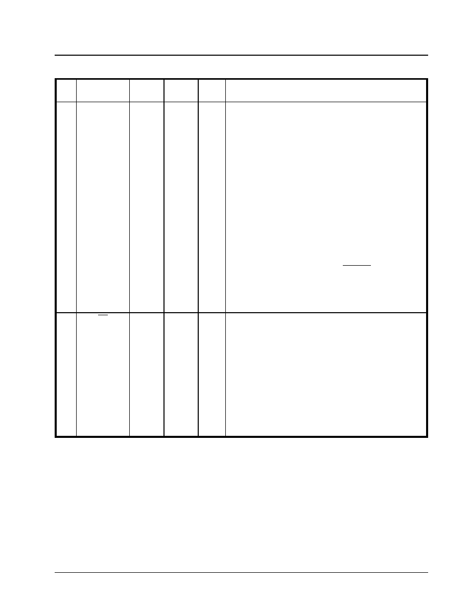
PIN DESCRIPTIONS (CONT.)
PIN
#
Signal
DTE
MODE
DCE
MODE
TYPE
FUNCTION
11
TX4A
RTSA
CTSA
O
Transmitter 4 ≠ Negative Data Differential Output to Line
The XRT4500 accepts a TTL binary data stream from the Terminal
Equipment via the TX4D (pin 8) input pin. The XRT4500 will convert
this data into either the V.10, V.11 or V.28 modes, and will output it
via this pin and TX4B (pin 10). The exact function of this output pin
depends upon whether the XRT4500 device is operating in the
DTE or DCE mode.
DTE Mode ≠ Negative Polarity portion of the RTS Line Signal.
DCE Mode ≠ Negative Polarity portion of the CTS Line Signal.
Note: If the XRT4500 has been configured to operate in either
the V.28/EIA-232 or V.10 Modes, then all of the data will be out-
put (to the line) in a single-rail manner via this output pin.
12
TX5A
DTRA
DSRA
O
Transmitter 5 ≠ Negative Data Differential Output to Line
The XRT4500 accepts a TTL binary data stream via the TX5D (pin
15) input pin. The XRT4500 will convert this data into either the
V.10, V.11 or V.28 modes, and will output it via this pin and TX5B
(pin 13). The exact function of this output pin depends upon
whether the XRT4500 device is operating in the DTE or DCE mode.
DTE Mode ≠ Negative Polarity portion of the DTR Line Signal.
Transmitter 5 accepts a TTL level binary data stream (as the
Data Terminal Read ≠ DTR) from the terminal equipment.
DCE Mode ≠ Negative Polarity portion of the DSR Line Signal.
Note: If the XRT4500 has been configured to operate in either
the V.28/EIA-232 or V.10 Modes, then all of the data will be out-
put (to the line) in a single-rail manner via this output pin.
13
TX5B
DTRB
DSRB
O
Transmitter 5 ≠ Positive Data Differential Output to Line
The XRT4500 accepts a TTL binary data stream via the TX5D (pin
15) input pin. The XRT4500 will convert this data into either the
V.10, V.11 or V.28 modes, and will output it via this pin and TX5A
(pin 12). The exact function of this output pin depends upon
whether the XRT4500 device is operating in the DTE or DCE mode.
DTE Mode
≠ Positive Polarity portion of DTR Line signal.
DCE Mode ≠ Positive Polarity portion of DSR Line signal.
Note: This output pin is not used if the XRT4500 has been con-
figured to operate in either the V.28/EIA-232 or V.10 Modes.
14
GND
Analog GND ≠ For Transmitters 4, 5, 6, 7, and 8.

·Á
·Á
·Á
·Á
XRT4500
MULTIPROTOCOL SERIAL NETWORK INTERFACE IC
REV. 1.0.7
7
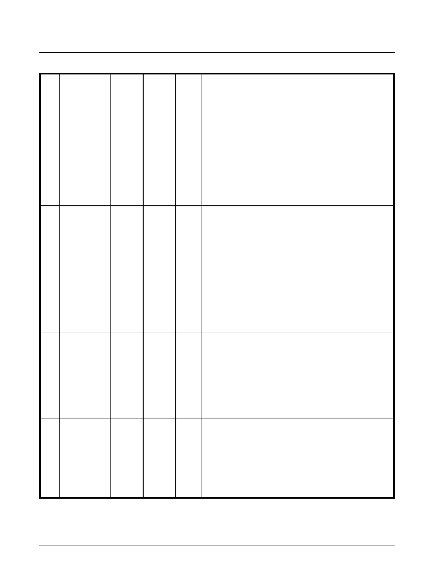
PIN DESCRIPTIONS (CONT.)
PIN
#
Signal
DTE
MODE
DCE
MODE
TYPE
FUNCTION
15
TX5D
D_DTR
D_DSR
I
Transmitter 5 ≠ Digital Data Input from Terminal Equipment
This input pin accepts a TTL level binary data stream, from the
local terminal equipment, and outputs it, in either a V.10, V.11 or
V.28 manner, via the TX5A (pin 12) and TX5B (pin 13) output
pins. The exact role that this input pin plays depends upon
whether the XRT4500 is operating in the DTE or DCE Modes.
DTE Mode ≠ Data Terminal Ready (DTR) Input Pin
If the XRT4500 is operating in the DTE mode, then this input pin
should be tied to the DTR output pin of the terminal equipment.
DCE Mode ≠ Data Set Ready (DSR) Input Pin
If the XRT4500 is operating in the DCE mode, then this input pin
should be tied to the DSR output pin of the terminal equipment.
Note: If the XRT4500 has been configured to operate in the
"Registered" Mode, then data applied to this input pin will be
latched (into the XRT4500) upon the rising edge of the
REG_CLK input signal.
16
VPP
+12V Power: This supply voltage is internally generated by the
Charge Pump Circuit within the XRT4500 device. If +12V is
available, then the external components can be eliminated.
17
TX8D
D_RL
D_RI
I
Transmitter 8 ≠ Digital Data Input from Terminal Equipment
This input accepts a TTL level binary data stream, from the local
terminal equipment, and outputs it, in either a V.10 or V.28 man-
ner via the TX8O (pin 19) output pin.
DCE Mode ≠ Ring Indicator (or Test Mode) Input Pin
If the XRT4500 has been configured to operate in the
DCE Mode ≠ This input pin should be connected to either the
"RI" (Ring Indicator) or the "TM" (Test Mode) indicator output pin
of the Terminal Equipment.
DTE Mode ≠ Remote Loop-back Indicator Input Pin
If the XRT4500 has been configured to operate in the
DTE Mode ≠ This input pin should be connected to the "RL"
(Remote Loop-back) indicator output pin of the Terminal Equip-
ment.
Note: If the XRT4500 has been configured to operate in the
"Registered" Mode, then data applied to this input pin will be
latched (into the XRT4500) upon the rising edge of the
REG_CLK input signal.

XRT4500
·Á
·Á
·Á
·Á
MULTIPROTOCOL SERIAL NETWORK INTERFACE IC
REV. 1.0.7
8
PIN DESCRIPTIONS (CONT.)
N
OTE
: Signal names beginning with D_ are digital signals.
N
OTE
: Signal names ending with B and A are the positive
and negative polarities of differential signals respectively.
PIN
#
Signal
DTE
MODE
DCE
MODE
TYPE
FUNCTION
18
LP
I
Loopback Command Input Pin ≠ Active Low:
This active-low input pin permits the user to configure the
XRT4500 into a "Loop-Back" Mode. The exact loop-back will
depend upon whether the XRT4500 is operating in the DTE or
DCE Modes.
Setting this input pin to "LOW" enables the Loop-back Operation.
Setting this input pin to "HIGH" disables the Loop-back Operation.
This input pin contains an Internal 20K
pull-up to VDD.
19
TX8O
RLA
RIA
O
Transmitter 8 ≠ Single Ended Data Output to Line
The XRT4500 accepts a TTL level binary data stream, from the
local terminal equipment via the "TX8D" input pin (pin 17), and
outputs it, in either a V.10 or V.28 manner via this output pin. The
exact role that this output pin plays depends upon whether the
XRT4500 is operating in the DTE or DCE Modes.
If the XRT4500 is configured to operate in the DCE Mode:
This output pin will typically drive the state of either the "RI"
(Ring Indicator) or "TM" (Test Mode) signals to the Remote
Terminal Equipment.
If the XRT4500 is configured to operate in the DTE Mode:
This output pin will typically drive the state of the "RL" (Remote
Loop-back) signal to the Remote Terminal Equipment.
20
VDD
Analog VDD ≠ For Receivers 4, 5, 6, 7 and 8.
21
CPP
Charge Pump Capacitor Pin: A 2.2µF tantalum capacitor must
be connected between pin 21 and pin 22.
22
CPM
Charge Pump Capacitor Pin: A 2.2µF tantalum capacitor must
be connected between pin 21 and pin 22.

·Á
·Á
·Á
·Á
XRT4500
MULTIPROTOCOL SERIAL NETWORK INTERFACE IC
REV. 1.0.7
9
PIN DESCRIPTIONS (CONT.)
PIN
#
Signal
DTE
MODE
DCE
MODE
TYPE
FUNCTION
23
RX8D
D_RI
D_RL
O
Receiver 8 ≠ Digital Data Output to Terminal Equipment
The XRT4500 receives a line signal (in either the V.10 or V.28
manner) via the RX8I input pin (Pin 25). The XRT4500 then con-
verts this data into a digital format (e.g., a CMOS level binary
data stream) and outputs it via this pin. The exact functionality of
this output pin depends upon whether the XRT4500 is operating
in the DCE or DTE Modes.
DCE Mode ≠ Remote Loop-back Indicator Output
If the XRT4500 has been configured to operate in the DCE
Mode ≠ This output pin should be connected to the "RL" (Remote
Loop-back) indicator input pin (of the Terminal Equipment).
DTE Mode ≠ Ring Indicator (or Test Mode Indicator) Output
If the XRT4500 has been configured to operate in the DTE
Mode ≠ This output pin should be connected to either the "RI"
(Ring Indicator) or "TM" (Test Mode) input pin of the Terminal
Equipment.
Notes: This output pin is tri-stated if the EN_OUT* input pin (pin
48) is "HIGH". If the XRT4500 has been configured to operate in
the "Registered" Mode, then data will be outputted via this pin,
upon the rising edge of the REG_CLK clock signal.
24
REG
I
Register Mode Control Select Input Pin:
This input pin permits the user to configure the XRT4500 to
operate in either the "Registered" Mode or in the "non-Regis-
tered" Mode. If the XRT4500 has been configured to operate in
the "Registered" Mode, then the following will happen.
∑ Data at the "TX5D" and "TX8D" input pins (Pins 15 & 17) will
be latched into the XRT4500 circuitry upon the rising edge of
the clock signal applied at the "REG_CLK" input pin.
∑ Data will be output via the "RX5D" and "RX8D" pins, upon the
rising edge of the clock signal applied at the "REG_CLK" input
pin.
If the XRT4500 has been configured to operate in the "Non-Reg-
istered" Mode, then the "REG_CLK" clock signal will have no
effect on the processing of signals via the "TX5D", "TX8D",
"RX5D" and "RX8D" pins.
Setting the "REG" input to "HIGH" configures the XRT4500 to
operate in the "Registered" Mode.
Setting the "REG" input to "LOW" configures the XRT4500 to
operate in the "Non-Registered" Mode.
This pin contains an internal 20K
pull-down to ground.

XRT4500
·Á
·Á
·Á
·Á
MULTIPROTOCOL SERIAL NETWORK INTERFACE IC
REV. 1.0.7
10
PIN DESCRIPTIONS (CONT.)
PIN
#
Signal
DTE
MODE
DCE
MODE
TYPE
FUNCTION
25
RX8I
RIA
RLA
I
Receiver 8 ≠ Line Input Pin:
This input pin accepts either a V.10 or V.28 type signal from the
line. Receiver 8 will then convert this signal into a "CMOS" level
(digital) signal and output this signal to the Terminal Equipment
via the RX8D output pin (Pin 23). The exact function of this out-
put pin depends upon whether the XRT4500 device is operating
in the DTE or DCE mode.
DTE Mode ≠ The RI line signal
DCE Mode ≠ The RL line signal
Notes:
1.
For some DTE applications, this input pin would accept
the "RI" (Ring Indicator) line signal (in either the V.10 or
V.28 format) form the DCE Terminal Equipment.
2. For some DCE applications, this input pin would accept the
"RL" (Remote Loop-back") line signal (in either the V.10 or
the V.28 format) from the DTE Terminal Equipment.
26
VSS
-6V Power: This supply voltage is internally generated by the
Switching Regulator Circuit within the XRT4500. The -6V is used
by receivers 4, 5, 6, 7 and 8. If a -6V supply is available, then the
external components can be eliminated.
27
TR7
LLA
LLA
I/0
Transceiver # 7 I/O Pins
The exact function of this pin depends upon whether the
XRT4500 is operating in the DCE or DTE Modes.
DTE Mode ≠ Transmitter 7 ≠ Single Ended Data Output to Line
Transceiver 7 accepts a CMOS level signal via the "TX76D" input
pin (pin 28). This digital data is converted into either a V.10 or
V.28 electrical signal; which is then output (via this pin), on the
line to the Remote Terminal Equipment.
DCE Mode ≠ Receiver 7 ≠ Single Ended Data Input from Line
This input pin accepts the line signal, from the Remote Terminal
Equipment, in a "single-ended" manner. This line signal is con-
verted into a CMOS level signal and is output (to the local Termi-
nal Equipment) via the "RX67D" output pin (Pin 32).
28
TX76D
D_LL
D_DCD
I
Digital Input ≠ Refer to Mode Control Tables, Table 3 & Table 4 .

·Á
·Á
·Á
·Á
XRT4500
MULTIPROTOCOL SERIAL NETWORK INTERFACE IC
REV. 1.0.7
11
PIN DESCRIPTIONS (CONT.)
PIN
#
Signal
DTE
MODE
DCE
MODE
TYPE
FUNCTION
29
TR6A
DCDA
DCDA
I/O
Transceiver # 6 Line Signal I/O Pin:
The exact function of this pin depends upon whether the
XRT4500 has been configured to operate in the DCE or DTE
Mode.
DTE Mode: Negative Polarity Input of DCD (Data Carrier
Detect) Signal:
This input pin (along with TR6B, pin 30) accepts the line signal,
from the remote terminal equipment, in either a Single-Ended or
Differential manner. This line signal is converted to CMOS level
signals and is outputted (to the local terminal equipment) via the
RX67D output pin (Pin 32).
DCE Mode: Negative Polarity Output Signal (of DCD-Data
Carrier Detect) to the Line:
Transceiver 6 accepts TTL level binary data stream, via the
"TX67D" (pin 28) input pin. This output pin, along with "TR6B"
(pin 30) will output this data to the Remote Terminal Equipment).
via an Analog Line Signal.
30
TR6B
DCDB
DCDB
I/O
Transceiver #6 Line Signal I/O Pin
The exact function of this pin, depends upon whether the
XRT4500 has been configured to operate in the DCE or DTE
Mode.
DTE Mode: Receiver 6 ≠ Positive Polarity Input of DCD (Data
Carrier Detect) Signal:
This input pin (along with TR6A, pin 29) accepts the line signal,
from the remote terminal equipment, in a Differential manner.
This line is converted to CMOS signal levels and is output (to the
local terminal equipment) via the RX67D output pin (Pin 32).
DCE Mode: Transmitter 6 ≠ Positive Polarity Output of DCD
(Data Carrier Data Signal) Pin:
Transceiver 6 accepts a TTL level binary data stream, via the
TX67D (pin 28) input pin. This output pin (along with TR6A, pin
29) will output this data (to the remote terminal equipment) via
an Analog line signal.
N
OTE
: This I/O pin is not used if the XRT4500 has been config-
ured to operate in the V.28/EIA-232 Communications Interface
Mode.
XRT4500
·Á
·Á
·Á
·Á
MULTIPROTOCOL SERIAL NETWORK INTERFACE IC
REV. 1.0.7
12
PIN DESCRIPTIONS (CONT.)
N
OTE
: Signal names beginning with D_ are digital signals.
N
OTE
: Signal names ending with B and A are the positive
and negative polarities of differential signals respectively.
PIN
#
Signal
DTE
MODE
DCE
MODE
TYPE
FUNCTION
31
DCE/DTE
LOW
HIGH
I
DCE/DTE Mode Select:
This input pin permits the user to configure the XRT4500 to
operate in either the DCE Mode or in the DTE Mode.
Logic 0: DTE Mode Operation
When the XRT4500 is configured to operate in the "DTE" Mode,
then "Transceiver # 3" will be configured to function as a
Receiver.
Logic 1: DCE Mode Operation
When the XRT4500 is configured to operate in the "DCE" Mode,
then "Transceiver # 3" will be configured to function as a Trans-
mitter. This input pin contains an internal 20K
pull-up to VDD.
32
RX67D
D_DCD
D_LL
O
Transceiver 6/7 Digital Output Pin:
The exact function of this pin depends upon whether the
XRT4500 has been configured to operate in the DCE or DTE
Mode.
DTE Mode ≠ Data Carrier Detect (DCD) Output Pin
When the XRT4500 is operating in the DTE Mode, this trans-
ceiver functions as a "line receiver". This line receiver accepts
either a V.10, V.28 or V.11 line signal via the TR6A and TR6B
pins (pins 29 and 30) and converts this line signal into a CMOS
level binary data stream. This binary data stream is output via
this pin. For DTE applications, this output pin should be con-
nected to the "DCD" input pin of the "Terminal Equipment".
DCE Mode ≠ Local Loop-back (LL) Indicator Output Pin
When the XRT4500 is operating in the DCE Mode, this trans-
ceiver functions as a "line receiver". This line receiver accepts
either a V.10, or V.28 line signal via the TR7 input pin (pin 27)
and converts this line signal into a CMOS level binary data
stream. This binary data stream is output via this pin. For DCE
applications, this input pin should be connected to the "LL" input
pin of the "Terminal Equipment".
·Á
·Á
·Á
·Á
XRT4500
MULTIPROTOCOL SERIAL NETWORK INTERFACE IC
REV. 1.0.7
13
PIN DESCRIPTIONS (CONT.)
N
OTE
: Signal names beginning with D_ are digital signals.
N
OTE
: Signal names ending with B and A are the positive
and negative polarities of differential signals respectively.
PIN
#
Signal
DTE
MODE
DCE
MODE
TYPE
FUNCTION
33
RX5D
D_DSR
D_DTR
O
Receiver 5 ≠ Digital Data Output to Terminal Equipment
The XRT4500 accepts a line signal (in either the V.10, V.11 or
V.28 manner) via the RX5A and RX5B input pins (Pins 35 & 36).
The XRT4500 then converts this data into digital format (e.g., a
CMOS level binary data stream) and outputs it to the Terminal
Equipment via this pin.
The exact role that this pin plays depends upon whether the
XRT4500 device is operating in the DCE or DTE modes.
DTE Mode ≠ Data Set Ready (DSR) Output Pin
For DTE applications, this output pin should be connected to the
"DSR" input of the Terminal Equipment.
DCE Mode ≠ Data Terminal Ready (DTR) Output Pin
For DCE applications, this output pin should be connected to the
"DTR" input pin of the Terminal Equipment.
Note:
1. This output pin is tri-stated if the EN_OUT input pin (pin 48)
is "HIGH".
2. If the XRT4500 has been configured to operate in the
"Registered" Mode, then data will be outputted via this pin
upon the rising edge of the "REG_CLK" clock signal.
34
EC
I
Echo Clock Mode Select Input Pin
This input pin permits the user to enable or disable the "Echo-
Clock" Mode feature within the XRT4500 device. If the user con-
figures the XRT4500 to operate in the "Echo-Clock" Mode, then
the RX3D output pin (Pin 73) will be internally looped into the
"TX2D" input pin (Pin 67).
Setting this input pin "LOW" enables the "Echo-Clock" Mode.
Setting this input pin "HIGH" disables the "Echo-Clock" Mode.
Note: The "Echo-Clock" Mode feature is only available if the
XRT4500 is operating in the DTE Mode.
This input pin contains an internal 20K
pull-up to VDD.
XRT4500
·Á
·Á
·Á
·Á
MULTIPROTOCOL SERIAL NETWORK INTERFACE IC
REV. 1.0.7
14
PIN DESCRIPTIONS (CONT.)
N
OTE
: Signal names beginning with D_ are digital signals.
N
OTE
: Signal names ending with B and A are the positive
and negative polarities of differential signals respectively.
PIN
#
Signal
DTE
MODE
DCE
MODE
TYPE
FUNCTION
35
RX5B
DSRB
DTRB
I
Receiver 5 ≠ Positive Data Differential Input from Line
The XRT4500 will accept either a V.10, V.11 or V.28 type signal via
this input pin, along with RX5A (Pin 36) and will generate a result-
ing CMOS level binary data stream, via the RX5D (Pin 33) output
pin. The exact function of this input pin depends upon whether the
XRT4500 device is operating in the DTE or DCE mode.
DTE Mode ≠ Positive polarity portion of the DSR line signal.
DCE Mode ≠ Positive polarity portion of the DTR line signal.
Note: This output pin is not used if the XRT4500 has been con-
figured to operate in either the V.28/EIA-232 or V.10 Modes.
36
RX5A
DSRA
DTRA
I
Receiver 5 ≠ Negative Data Differential Input from Line
The XRT4500 will accept either a V.10, V.11 or V.28 type signal
via this input pin, along with RX5B (pin 35) and will generate a
resulting CMOS level binary data stream, via the RX5D (Pin 33)
output pin. The exact function of this input pin depends upon
whether the XRT4500 device is operating in the DTE or DCE
mode.
DTE Mode ≠ Negative polarity portion of the DSR line signal.
DCE Mode ≠ Negative polarity portion of the DTR line signal.
Note: If the XRT4500 has been configured to operate in either
the V.28/EIA-232 or V.10 Modes, then all of the data will be out-
put (to the line) in a single-rail manner via this output pin.
37
RX4A
CTSA
RTSA
I
Receiver 4 ≠ Negative Data Differential Input from Line
The XRT4500 will accept either a V.10, V.11 or V.28 type signal
via this input pin, along with RX4B (pin 38) and will generate a
resulting CMOS level binary data stream, via the RX4D output
pin (Pin 40). The exact function of this input pin depends upon
whether the XRT4500 device is operating in the DTE or DCE
mode.
Note: If the XRT4500 has been configured to operate in either
the V.28/EIA-232 or V.10 Modes, then all of the data will be out-
put (to the line) in a single-rail manner via this output pin.
38
RX4B
CTSB
RTSB
I
Receiver 4 ≠ Positive Data Differential Input from Line
The XRT4500 will accept either a V.10, V.11 or V.28 type signal
via this input pin, along with RX4A (pin 37) and will generate a
resulting CMOS level binary data stream, via the RX4D output
pin (Pin 40). The exact function of this input pin depends upon
whether the XRT4500 device is operating in the DTE or DCE
mode.
N
OTE
: This output pin is not used if the XRT4500 has been con-
figured to operate in either the V.28/EIA-232 or V.10 Modes.
·Á
·Á
·Á
·Á
XRT4500
MULTIPROTOCOL SERIAL NETWORK INTERFACE IC
REV. 1.0.7
15
PIN DESCRIPTIONS (CONT.)
N
OTE
: Signal names beginning with D_ are digital signals.
N
OTE
: Signal names ending with B and A are the positive
and negative polarities of differential signals respectively.
PIN
#
Signal
DTE
MODE
DCE
MODE
TYPE FUNCTION
39
SLEW_CNTL
O
V.28/V.10 Slew-Rate Control Pin ≠ This pin permits the user to
specify the slew rate of the V.10 or V.28 output driver. The user
accompanies this by connecting a resistor (of a specific value)
between this pin and ground.
Figure 34 presents a plot which depicts the relationship
between the `Rise/Fall Time' of a V.10 output signal (from the
XRT4500) and the value of this resistor.
Figure 35 presents a plot which depicts the relationship
between the slew-rate (expressed in terms of V/µs) of a V.28 out-
put signal (from the XRT4500) and the value of this resistor.
40
RX4D
D_CTS
D_RTS
O
Receiver 4 ≠ Digital Data Output to Terminal Equipment
This output pin is the digital (CMOS level) representation of the
line signal that is applied to the RX4A (pin 37) and RX4B (pin 38)
input pins.
The exact role that this pin plays depends upon whether the
XRT4500 is operating in the DCE or DTE Mode.
DCE Mode ≠ CTS (Clear to Send) Output Signal
For DCE Mode applications, this output pin should be connected
to the "CTS" input pin of the Terminal Equipment.
DTE Mode ≠ RTS (Request to Send) Output Signal
For DTE Mode applications, this output pin should be connected
to the "RTS" input pin of the Terminal Equipment.
41
Vsense
I
Switching Regulator ≠ Voltage sense input
42
Isense
I
Switching Regulator ≠ Current sense input
43
GND_REG
Switching Regulator Ground
44
LATCH
I
Mode Control Input Latch Enable ≠ Logic 0:
This input pin permits the user to latch the states of the Mode
Control Input pins (4, 5, and 6) (M0, M1, and M2) into the
XRT4500 circuitry. This feature frees up the signals (driving the
Mode Control Input pins) for other purposes.
Driving this input, from "low" to "high" latches the contents of the
Mode Control pins of the XRT4500 (into the XRT4500 circuitry).
For the duration that the LATCH input pin is "high", the user can
change the state of the signals controller the M0, M1 and M2
input pins, without effecting the operation of the XRT4500.
45
CLKFS
O
Internally Generated 500kHz Clock ≠ This clock signal is inter-
nally used to drive both the switching regulator and the digital
`Glitch' filters. The user is advised to leave this pin floating.

XRT4500
·Á
·Á
·Á
·Á
MULTIPROTOCOL SERIAL NETWORK INTERFACE IC
REV. 1.0.7
16
PIN DESCRIPTIONS (CONT.)
N
OTE
: Signal names beginning with D_ are digital signals.
N
OTE
: Signal names ending with B and A are the positive
and negative polarities of differential signals respectively.
PIN
#
Signal
DTE
MODE
DCE
MODE
TYPE
FUNCTION
46
E_232H
I
High Speed RS-232 Enable ≠ Logic 0 enables high speed RS-
232 mode (drives 3K
in parallel with 1000pF at 256 KHz).
Internal 20K
pull-up to VDD.
This input pin permits the user to either enable or disable the
`High-Speed RS-232 Driver' feature. The non high speed mode
provides a 120 Kbps clock rate.
Note: This pin setting applies to all `RS-232/V.28 Drivers' within
the XRT4500.
47
V
DD
Analog VDD for the Internal Switching Regulator
48
EN_OUT
I
Output Enable Pin for Receiver 5 and 8
This active-low output pin permits the user to tri-state the
"RX5D" and "RX8D" output pins (Pins 23 & 33).
Setting this input pin "low" causes the XRT4500 to tri-state the
"RX5D" and "RX8D" output pins. Conversely, setting this input
pin "high" enables the "RX5D" and the "RX8D" output drivers for
signal transmission to the local Terminal Equipment.
This input pin contains an internal 20k
pull-down resistor to
ground.
49
REG_CLK
I
Register Mode Clock Input Signal:
If the XRT4500 has been configured to operate in the "Regis-
tered" Mode, then a rising clock edge at this input causes the
XRT4500 to do the following.
∑
Data at the TX5D and TX8D input pins (Pins 15 & 17) will be
latched into the XRT4500 circuitry.
∑
Data will be outputted via the RX5D and RX8D pins (Pins 23
& 33).
This input pin has no function when the XRT4500 is operating in
the "Non-Registered" Mode. The user configures the XRT4500
to operate in the "Registered" Mode, by pulling the "REG" input
pin to V
DD
.
This input pin contains an internal 20k
pull-up to V
DD
.

·Á
·Á
·Á
·Á
XRT4500
MULTIPROTOCOL SERIAL NETWORK INTERFACE IC
REV. 1.0.7
17
PIN DESCRIPTIONS (CONT.)
N
OTE
: Signal names beginning with D_ are digital signals.
N
OTE
: Signal names ending with B and A are the positive
and negative polarities of differential signals respectively.
PIN
#
Signal
DTE
MODE
DCE
MODE
TYPE
FUNCTION
50
2CK/3CK
I
2 or 3 Clock Select Input Pin
This input pin permits the XRT4500 to operate in either the "2
Clock" or "3 Clock" Mode. If the XRT4500 is configured to oper-
ate in the `2-Clock' mode, then the XRT4500 will synthesize the
`RX2D' Clock signal, from the clock signal applied at the `TX3D'
input pin. Conversely, if the XRT4500 is configured to operate in
the `3 Clock' Mode, then the XRT4500 will synthesize the `RX2D'
Clock signal from the live signal received via `RX2A' and `RX2B'
input pin. Setting this input pin "high" configures the XRT4500 to
operate in the "2 Clock" Mode. Conversely, setting this input pin
"low" configures the XRT4500 to operate in the "3 Clock" Mode.
Note:
1. This input pin is ignored if the XRT4500 is configured to
support the X.21 Communications Interface.
Logic Don't Care: 1 Clock When in the X.21 Mode (M2, M1, M0 = 011)
Logic 0: 3 Clocks When Mode
X.21 (M2, M1, M0
011)
Logic 1: 2 Clocks When Mode
X.21 (M2, M1, M0
011)
N
OTE
:
2. This input pin is ignored if the XRT4500 is configured to
operate in the DTE Mode.
This input pin contains an internal 20k
pull-up to V
DD
.
51
VDD_REG
Analog VDD ≠ Charge pump and switching regulator output
drivers
52
SR_OUT
O
Switching Regulator ≠ Inductor driver output

XRT4500
·Á
·Á
·Á
·Á
MULTIPROTOCOL SERIAL NETWORK INTERFACE IC
REV. 1.0.7
18
PIN DESCRIPTIONS (CONT.)
PIN
#
Signal
DTE
MODE
DCE
MODE
TYPE
FUNCTION
53
OSCEN
I
Test Oscillator Enable ≠ Active Low;
This active-low input pin permits the user to enable or disable the
"Internal Oscillator" within the XRT4500. If the user enables this fea-
ture then the XRT4500 will begin generating a clock signal via both
the RX2D and RX3D output pins. The frequency of this clock signal
ranges between 32kHz and 64kHz.
This clock signal can be used to support "Stand-Alone DTE Diag-
nostic" Testing.
Setting this input to "0" enables the "Internal Oscillator".
Setting this input to "1" disables the "Internal Oscillator".
Note: The "Internal Oscillator" is only available if the XRT4500 is
operating in the DTE Mode.
If LP = "0" The Clock Signal (32 - 64kHz) is available on Rx3D.
If LP = "0" and EC = "0" the clock signal is available on RX2D.
N
OTE
: This input pin contains an internal 20k
pull-up to V
DD
.
54
CLKINV
I
Invert Clock Input Pin ≠ This `Active -Low' input pin permits the
user to either enable or disable the `Clock/Inversion' feature. The
exact manifestation of the `Clock Inversion' feature depends upon
whether the XRT4500 is operating in the `DCE' or `DTE' Mode.
If the XRT4500 is operating in the DTE Mode, then the RX3D output
signal (which is receiving the TXC signal) will be inverted before it is
outputted to the terminal equipment.
If the XRT4500 is operating in the DCE Mode, then the TX3D input
signal (which is transmitting the TXC signal) will be inverted before it
converted into the analog format and is output to the line.
Setting this input pin `Low' enables the `Clock Inversion' feature.
Conversely, setting this input pin `High' disables this feature.
N
OTE
: This input pin contains an internal 20k
pull-up to V
DD
.
55
DTINV
I
Invert Data ≠ Active Low; Logic 0: Data Inverted.
Logic 1: Data not Inverted. Internal 20K
pull-up V
DD
.
56
VSS_T123
-6V Power Supply Signal: This supply voltage is internally gener-
ated by the Switching Regulator Circuit within the XRT4500.
57
GND
Digital Ground: for transmitters 1, 2, and 3
58
VDD_T123
Analog VDD: for transmitters 1, 2, and 3
59
GND_T12
Analog Ground: Transmitters 1 and 2

·Á
·Á
·Á
·Á
XRT4500
MULTIPROTOCOL SERIAL NETWORK INTERFACE IC
REV. 1.0.7
19
PIN DESCRIPTIONS (CONT.)
PIN
#
Signal
DTE
MODE
DCE
MODE
TYPE
FUNCTION
60
TX1D
D_TXD
D_RXD
I
Transmitter 1 ≠ Digital Data Input from Terminal Equipment.
The exact role that this input pin plays depends upon whether
the XRT4500 is operating in the DTE or DCE Modes.
DTE Mode ≠ TXD (Transmit Data) Input:
The DTE Terminal Equipment is expected to apply the TXD
(Transmit Data) to this input pin.
The XRT4500 will convert this binary data stream into either the
V.35, V.11, or V.28 format and will output this data via the TX1A
and TX1B output pin.
DCE Mode ≠ RXD (Receive Data) Input:
The DCE Terminal Equipment is expected to apply the RXD
(Receive Data) to this input pin.
The XRT4500 will convert this binary data stream into either the
V.35, V.11 or V.28 format and will output this data via the TX1A
and TX1B output pins.
61
CM_TX1
O
AC GND- Transmitter 1 Output Termination center tap in V.35
Mode. Connect a 0.1µF capacitor to ground.
62
TX1B
TXDB
RXDB
O
Transmitter 1 ≠ Positive Data Differential Output to line.
The exact function of this output pin depends upon whether the
XRT4500 is operating in the DCE or DTE Modes.
DTE Mode: Transmit Data (TXD) ≠ Positive Polarity Output
Line Signal
Transmitter 1 accepts a TTL Level binary data stream (as the
"Transmit Data" ≠ TXD) from the DTE Terminal Equipment.
Transmitter 1 converts this digital data into any of the following
electrical formats: V.10, V.11, V.28 and V.35, prior to transmis-
sion to the line.
If this data is being converted into either the V.11 or V.35 format,
then this pin outputs the positive-polarity portion of the "TXD"
data to the line. If this data is being converted into either the V.10
or V.28 formats, then this pin is inactive.
DCE Mode: Receive Data (RXD) ≠ Positive Polarity Output
Line Signal
Transmitter 1 accepts a CMOS (or TTL) level signal binary data
stream (as the "Receive Data" ≠ RXD) from the DCE Terminal
Equipment. Transmitter 1 converts this digital data into any of the
following electrical formats: V.10, V.11, V.28 and V.35 prior to
transmission to the line.
If this data is being converted into either the V.11 or V.35 format,
then this pin outputs the positive polarity portion of the "RXD"
data to the line. If this data is being converted into either the V.10
or V.28 formats, then this pin is inactive.

XRT4500
·Á
·Á
·Á
·Á
MULTIPROTOCOL SERIAL NETWORK INTERFACE IC
REV. 1.0.7
20
PIN DESCRIPTIONS (CONT.)
PIN
#
Signal
DTE
MODE
DCE
MODE
TYPE
FUNCTION
63
TX1A
TXDA
RXDA
O
Transmitter 1 ≠ Negative Data Differential Output to Line
The exact function of this output pin depends upon whether the
XRT4500 is operating in the DCE or DTE Modes.
DTE Mode: Transmit Data (TXD) ≠ Negative Polarity Output
Signal
Transmitter 1 accepts a TTL level binary data stream (as the
"Transmit Data" ≠ TXD) from the DTE Terminal Equipment. Trans-
mitter 1 converts this digital data into any of the following electrical
formats: V.10, V.11, V.28 and V.35 prior to transmission to the line.
If this data is being converted into either the V.11 or V.35 format,
then this pin outputs the negative-polarity portion of the "TXD"
data to the line. If this data is being converted into either the V.10
or V.28 formats, then this pin outputs this data to the line in a sin-
gle-ended manner.
DCE Mode: Receive Data (RXD) ≠ Negative Polarity Output
Line Signal
Transmitter 1 accepts a TTL level binary data stream (as the
"Receive Data" ≠ RXD) from the DCE Terminal Equipment.
Transmitter 1 converts this digital data into any of the following
electrical formats: V.10, V.11, V.28 and V.35 prior to transmission
to the line.
If this data is being converted into either the V.11 or V.35 format,
then this pin outputs the negative-polarity portion of the "RXD"
data to the line. If this data is being converted into either the V.10
or V.28 formats, then this pin outputs this data to the line in a sin-
gle-ended manner.

·Á
·Á
·Á
·Á
XRT4500
MULTIPROTOCOL SERIAL NETWORK INTERFACE IC
REV. 1.0.7
21
PIN DESCRIPTIONS (CONT.)
PIN
#
Signal
DTE
MODE
DCE
MODE
TYPE
FUNCTION
64
TX2A
SCTEA
RXCA
O
Transmitter 2 ≠ Negative Data Differential Output to Line
The exact function of this output pin depends upon whether the
XRT4500 is operating in the DCE or DTE Mode.
DTE Mode Transmit Clock Echo (SCTE) ≠ Negative Polarity
Output Signal
Transmitter 2 accepts a TTL level binary data system (as the
`Transmit Clock Echo' ≠ SCTE) from the DTE terminal equip-
ment. Transmitter 2 converts this digital data into any of the fol-
lowing electrical formats: V.10, V.11, V.28 or V.35 prior to
transmission to the line.
If this data is being converted into the V.11 or V.35 electrical format
then this pin outputs the `Negative Polarity' portion of the `SCTE'
data to the line. If this data is being converted into the V.10 or V.28
electrical format, tthen this pin outputs this data to the line in a
single-ended manner.
DCE Mode Receive Clock (RXC) Signal ≠ Negative Polarity
Output Line Signal
Transmitter 2 accepts a TTL level binary data system (as the
`Receive Clock - RXC) from the DCE terminal equipment. Trans-
mitter 2 converts this digital data into any of the following electrical
formats: V.10, V.11, V.28 or V.35 prior to transmission to the line
.
If this data is being converted into the V.11 or V.35 electrical for-
mat then this pin outputs the `Negative Polarity' portion of the
`RXC' data to the line. If this data is being converted into the V.10
or V.28 electrical format, then this pin outputs this data to the line
in a single-ended manner.

XRT4500
·Á
·Á
·Á
·Á
MULTIPROTOCOL SERIAL NETWORK INTERFACE IC
REV. 1.0.7
22
65
TX2B
SCTEB
RXCB
O
Transmitter 2 ≠ Positive Data Differential Output to line.
The exact function of this output pin depends upon whether the
XRT4500 is operating in the DCE or DTE Mode.
DTE Mode Transmit Clock Echo (SCTE) ≠ Positive Polarity
Output Signal
Transmitter 2 accepts a TTL level binary data system (as the
`Transmit Clock Echo' ≠ SCTE) from the DTE terminal equip-
ment. Transmitter 2 converts this digital data into any of the fol-
lowing electrical formats: V10, V.11, V.28 or V.35 prior to
transmission to the line.
If this data is being converted into the V.11 or V.35 electrical format
then this pin outputs the `Positive Polarity' portion of the `SCTE'
data to the line. If this data is being converted into the V.10 or V.28
electrical format, then this output pin is in-active.
DCE Mode Receive Clock (RXC) Signal ≠ Positive Polarity
Output Line Signal
Transmitter 2 accepts a TTL level binary data system (as the
`Receive Clock - RXC) from the DCE terminal equipment. Trans-
mitter 2 converts this digital data into any of the following electrical
formats: V.10, V.11, V.28 or V.35 prior to transmission to the line
.
If this data is being converted into the V.11 or V.35 electrical for-
mat then this pin outputs the `Positive Polarity' portion of the
`RXC' data to the line. If this data is being converted into the V.10
or V.28 electrical format, then this output pin is in-active.
66
CM_TX2
O
Transmitter 2 Output Termination Center Tap in V.35 Mode ≠
This pin should be by-passed to ground with an external 0.1µF
capacitor.
PIN
#
Signal
DTE
MODE
DCE
MODE
TYPE
FUNCTION
·Á
·Á
·Á
·Á
XRT4500
MULTIPROTOCOL SERIAL NETWORK INTERFACE IC
REV. 1.0.7
23
PIN DESCRIPTIONS (CONT.)
PIN
#
Signal
DTE
MODE
DCE
MODE
TYPE
FUNCTION
67
TX2D
D_SCTE
D_RXC
I
Transmitter 2 ≠ Digital Data Input from Terminal Equipment
The exact role that this input pin plays, depends upon whether
the XRT4500 is operating in the DTE or DCE Mode.
DTE Mode: SCTE (Transmit Clock Echo) Input
The Serial Communications Controller (at the DTE Terminal) is
expected to derive the SCTE (Transmit Clock Echo) clock signal,
from the TXC signal, and input it (into the XRT4500) via this
input pin. The XRT4500 will convert this binary data stream into
either the V.35, V.11 or V.28 format and will output this data via
the TX2A and TX2B output pins.
DCE Mode: RXC (Receive Clock) Input
The Serial Communications Controller (at the DCE Terminal) is
expected to apply the RXC clock signal to this input pin. The
XRT4500 will convert this binary data stream into either the V.35,
V.11 or V.28 format and will output this data via the TX2A and
TX2B output pins.
Note: If the XRT4500 has been configured to operate in both the
DTE and the "Echoed Clock" Mode, then the XRT4500 will
ignore this input pin and will instead use the clock signal which is
output via the "D_TXC" output pin (e.g., RX3D or pin 73).
68
TX3D
D_X
D_TXC
I
Transmitter 3 ≠ Digital Data Input from Terminal Equipment
The exact role that this pin plays depends upon whether the
XRT4500 is operating in the DCE or DTE Modes.
DTE Mode: This input pin is not used
DCE Mode: TXC ≠ Transmit Clock Signal
This input pin functions as the "TXC" (Transmit Clock) input signal
from the DCE Terminal. The XRT4500 will convert this "digital"
clock data into either the V.35, V.11 or V.28 format and will output
this data via the TR3A and TR3B output pins.
69
CM_TR3
O
DTE Mode: AC GND ≠ Transmitter 3 Output Termination center
tap in V.35 Mode. Connect a 0.1µF capacitor to ground.
DCE Mode: AC GND ≠ Receiver 3 Input Termination center tap
in V.35 Mode. Connect a 0.1µF capacitor to ground.
70
TR3A
TXCA
TXCA
I/O
DTE Mode: Receiver 3 ≠ Negative Data Differential Input from
Line
DCE Mode: Transmitter 3 ≠ Negative Data Differential Output
to Line.
71
TR3B
TXCB
TXCB
I/O
DCE Mode: Transmitter 3 ≠ Positive Data Differential Output to Line.
DTE Mode: Receiver 3 ≠ Positive Data Differential Input from Line.

XRT4500
·Á
·Á
·Á
·Á
MULTIPROTOCOL SERIAL NETWORK INTERFACE IC
REV. 1.0.7
24
PIN DESCRIPTIONS (CONT.)
PIN
#
Signal
DTE
MODE
DCE
MODE
TYPE
FUNCTION
72
GND
Analog GND: Receivers 4, 5, 6, 7 and 8
73
RX3D
D_TXC
D_X
O
Receiver 3 ≠ Digital Output to Terminal Equipment:
This output pin is the digital (CMOS level) representation of the
line signal that is received via the TR3A (pin 70) and TR3B (pin
71) input pins.
The exact role that this pin plays depends upon whether the
XRT4500 is operating in the DCE or DTE Mode.
DTE Mode: TXC ≠ Transmit Clock Signal
This output pin functions as the "TXC" (Transmit Clock) output
signal to the Terminal Equipment. The DTE Terminal Equipment
will typically use this signal to synthesize the SCTE clock signal.
DCE Mode: This output pin is NOT used.
Note: If the "Internal Oscillator" (within the XRT4500) is enabled,
then this pin will output a 32kHz to 64kHz clock signal. This clock
signal can be used for "Stand-Alone DTE Diagnostic" Testing.
74
RX2D
R_RXC
D_SCTE
O
Receiver 2 ≠ Digital Data Output to Equipment
This output pin is the digital (CMOS level) representation of the
line signal that is received via the RX2A (pin 77) and RX2B (pin
76) input pins.
The exact role that this pin plays depends upon whether the
XRT4500 is operating in the DCE or DTE Modes.
DCE Mode: SCTE ≠ Transmit Clock Echo Signal:
This output pin functions as the SCTE (Transmit Clock Echo)
output signal to the Terminal Equipment. The DCE Terminal
Equipment will typically use this clock signal to sample the "TXD"
(Transmit Data).
DTE Mode: RXC ≠ Receive Clock Signal:
This output pin functions as the "RXC" (Receive Clock) output
signal to the Terminal Equipment. The DTE Terminal Equipment
will typically use this signal to sample the "RXD" (Receive Data).
Note: If the "Internal Oscillator" (within the XRT4500) is enabled,
then this pin will output a 32kHz ≠ 64kHz clock signal. This clock
signal can be used for "Stand-Alone DTE Diagnostic" testing.
75
EN_FLTR
I
Enable Glitch Filter on Receiver 4, 5, 6, 7, 8 inputs. Internal
20k
pull-down
76
RX2B
RXCB
SCTEB
I
Receiver 2 ≠ Positive Data Differential Input from Line
77
RX2A
RXCA
RXCB
I
Receiver 2 ≠ Negative Data Differential Input from Line

·Á
·Á
·Á
·Á
XRT4500
MULTIPROTOCOL SERIAL NETWORK INTERFACE IC
REV. 1.0.7
25
PIN DESCRIPTIONS
PIN
#
Signal
DTE
MODE
DCE
MODE
TYPE
FUNCTION
78
RX1A
RXDA
TXDA
I
Receiver 1 ≠ Negative Data Differential Input from Line
79
RX1B
RXDB
TXDB
I
Receiver 1 ≠ Positive Data Differential Input from Line
The exact function of this input pin depends upon whether the
XRT4500 is operating in the DCE or DTE Mode. This input pin,
along with "RX1A" (pin 78) will accept a line signal in either the
V.35, V.11, V.28/EIA-232 or V.10 electrical format. Receiver 1 will
then convert this line signal into a CMOS level binary data
stream, and will output this data (to the Terminal Equipment) via
the "RX1D" output pin (pin 1).
DCE Mode ≠ Receive Data (RXD) ≠ Negative Polarity Input
Line Signal
80
EN_TERM
I
Enable Input Termination for Receiver 1, 2, 3, in V.11 Mode.
Internal 20k
pull-down to ground.

XRT4500
·Á
·Á
·Á
·Á
MULTIPROTOCOL SERIAL NETWORK INTERFACE IC
REV. 1.0.7
26
ELECTRICAL CHARACTERISTICS
N
OTES
:
1. Absolute Maximum Ratings are those beyond
which the safety of a device may be impaired.
2. All currents into device pins are positive; all cur-
rents out of device are negative. All voltages are
referenced to device ground unless otherwise
specified.
3. The efficiency of the switching regulator and the
charge pump is approximately 70%. The actual
power dissipation of the XRT4500 at 5V, with maxi-
mum loading, is 660mW in V.10, 700mW in V.11,
950mW in V.35 and 800mW in the V.28 mode. In
the "Reduced Power Mode" the XRT4500 chip dis-
sipation is 310mW.
4. "Typical Load" is the corresponding receiver in
another XRT4500 operating in the DTE mode.
5. A 50% duty cycle square wave, at the specified fre-
quency in the table, is applied to all Clock and Data
lines of the High Speed Transmitters).
6. A 10 KHz 50% duty cycle square wave is applied to
all Handshake Lines (Low Speed Transmitters).
Supply Voltage
M
IN
T
YP
M
AX
UNITS
T
EST
C
ONDITIONS
Vpp +12V Supply
11
12
13
V
Full Load on V.28
Vss
-5.7
-6.0
-6.3
V
Full Load on V.28
IDD in DCE Mode- Ta=25∞C, VDD=5V, Data and Clock at maximum operating frequencies unless other-
wise specified
P
ARAMETER
M
IN
T
YP
M
AX
UNITS
T
EST
C
ONDITIONS
V.10
M0=0, M1=0, M2=0
145
160
180
160
180
200
190
215
240
mA
No Load or Signal, Tx Digital Inputs tied High
Typical Load at 10 kHz
Typical Load at 50 kHz
EIA-530-A (V.11)
M0=1, M1=0, M2=0
125
205
230
275
140
230
255
305
170
275
305
365
mA
No Load or Signal, Tx Digital Inputs tied High
Typical Load at 1 MHz
Typical Load at 4 MHz
Typical Load at 10 MHz
EIA-530, RS449, V.36
M0=0, M1=1, M2=0
120
195
225
270
135
215
250
300
160
260
300
360
mA
No Load or Signal, Tx Digital Inputs tied High
Typical Load at 1 MHz
Typical Load at 4 MHz
Typical Load at 10 MHz
X.21
M0=1, M1=1, M2=0
115
195
215
260
130
215
240
290
155
260
290
350
mA
No Load or Signal, Tx Digital Inputs tied High
Typical Load at 1 MHz
Typical Load at 4 MHz
Typical Load at 10 MHz
V.35
M0=0, M1=0, M2=1
215
255
265
290
240
285
295
320
290
340
355
385
mA
No Load or Signal, TX Digital Inputs tied High
Typical Load at 1 MHz
Typical Load at 4 MHz
Typical Load at 10 MHz
RESERVED
M0=1, M1=0, M2=1
120
200
225
270
135
225
250
300
160
270
300
360
mA
No Load or Signal, Tx Digital Inputs tied High
Typical Load at 1 MHz
Typical Load at 4 MHz
Typical Load at 10 MHz
RS-232 (V.28)
M0=0, M1=1, M2=1
115
215
225
130
240
250
155
290
300
mA
No Load or Signal, Tx Digital Inputs tied High
Typical Load at 10 kHz
Typical Load at 100 kHz
POWER DOWN
M0=1, M1=1, M2=1
80
90
110
mA
Reduced Power Mode

·Á
·Á
·Á
·Á
XRT4500
MULTIPROTOCOL SERIAL NETWORK INTERFACE IC
REV. 1.0.7
27
7. Input termination is enabled on High Speed V.11
Receivers.
N
OTES
:
1. Absolute Maximum Ratings are those beyond
which the safety of a device may be impaired.
2. All currents into device pins are positive; all cur-
rents out of device are negative. All voltages are
referenced to device ground unless otherwise
specified.
3. The efficiency of the switching regulator and the
charge pump is approximately 70%. The actual
power dissipation of the XRT4500 at 5V, with maxi-
mum loading, is 660mW in V.10, 700mW in V.11,
950mW in V.35 and 800mW in the V.28 mode. In
the "Reduced Power Mode" the XRT4500 chip dis-
sipation is 310mW.
4. "Typical Load" is the corresponding receiver in
another XRT4500 operating in the DCE mode.
5. A 50% duty cycle square wave, at the specified fre-
quency in the table, is applied to all Clock and Data
lines of the High Speed Transmitters).
6. A 10 KHz 50% duty cycle square wave is applied to
all Handshake Lines (Low Speed Transmitters).
7. Input termination is enabled on High Speed V.11
Receivers.
IDD in DTE Mode - Ta=25∞C, VDD=5V, Data and Clock at maximum operating frequencies unless other-
wise specified
P
ARAMETER
M
IN
T
YP
M
AX
UNITS
T
EST
C
ONDITIONS
V.10
M0=0, M1=0, M2=0
145
160
170
160
180
190
190
215
230
mA
No Load or Signal, Tx Digital Inputs tied High
Typical Load at 10 kHz
Typical Load at 50 kHz
EIA-530-A (V.11)
M0=1, M1=0, M2=0
130
190
210
250
145
210
235
280
175
250
280
335
mA
No Load or Signal, Tx Digital Inputs tied High
Typical Load at 1 MHz
Typical Load at 4 MHz
Typical Load at 10 MHz
EIA-530, RS449, V.36
M0=0, M1=1, M2=0
125
180
205
245
140
200
230
275
170
240
275
330
mA
No Load or Signal, Tx Digital Inputs tied High
Typical Load at 1 MHz
Typical Load at 4 MHz
Typical Load at 10 MHz
X.21
M0=1, M1=1, M2=0
120
170
190
230
130
190
210
255
155
230
250
305
mA
No Load or Signal, Tx Digital Inputs tied High
Typical Load at 1 MHz
Typical Load at 4 MHz
Typical Load at 10 MHz
V.35
M0=0, M1=0, M2=1
180
220
235
255
200
245
260
285
240
295
310
340
mA
No Load or Signal, Tx Digital Inputs tied High
Typical Load at 1 MHz
Typical Load at 4 MHz
Typical Load at 10 MHz
RESERVED
M0=1, M1=0, M2=1
125
185
205
245
140
205
230
275
170
245
275
330
mA
No Load or Signal, Tx Digital Inputs tied High
Typical Load at 1 MHz
Typical Load at 4 MHz
Typical Load at 10 MHz
RS-232 (V.28)
M0=0, M1=1, M2=1
115
200
205
130
220
230
155
265
275
mA
No Load or Signal, Tx Digital Inputs tied High
Typical Load at 10 kHz
Typical Load at 100 kHz
POWER DOWN
M0=1, M1=1, M2=1
80
90
110
mA
Reduced Power Mode

XRT4500
·Á
·Á
·Á
·Á
MULTIPROTOCOL SERIAL NETWORK INTERFACE IC
REV. 1.0.7
28
TA = 25∞C, VDD = 5V, VSS = -6V, VPP = 12V, M
AXIMUM
O
PERATING
F
REQUENCY
U
NLESS
O
THERWISE
S
PECIFIED
S
YMBOL
P
ARAMETER
M
IN
T
YP
M
AX
U
NITS
M
ODE
I
NTERFACE
/C
ONDITIONS
S
UPPLY
C
URRENTS
M0
M1
M2
T
EST
C
ONDITIONS
I
DD
V
DD
Supply Current
(DCE Mode, All Digital
Pins = GND or V
DD
)
27
32
mA
0
0
0
V.10, No Load, No Signal
75
90
mA
0
0
0
V.10, Full Load, w/ Signal
27
32
mA
1
0
0
EIA-530A, No Load,
(V.11)
230
270
mA
1
0
0
EIA-530A, Full Load,
(V.11)
65
75
mA
0
0
1
V.35, No Load on V.28
Drivers
68
80
mA
0
0
1
V.35, Full Load on V.28
Drivers
20
25
mA
0
1
1
RS232, No Load
26
32
mA
0
1
1
RS232, Full Load
16
20
mA
1
1
1
Reduced Power Mode
E
LECTRICAL
C
HARACTERISTICS
(C
ONTIUED
)
S
YMBOL
P
ARAMETER
M
IN
T
YP
M
AX
U
NIT
C
ONDITIONS
L
OGIC
I
NPUTS
VIH
Logic Input High Voltage
2
V
TTL Compatible
V
IL
Logic Input Low Voltage
0.8
V
TTL Compatible
I
IN
Logic Input Current
±250
µ
A
With 20k
internal pull-up/down
resistor to ground
L
OGIC
O
UTPUTS
V
OH
Output High Voltage
3
4.5
V
I
O
= -4mA, TTL/CMOS
Compatible
V
OL
Output Low Voltage
0.3
0.8
V
I
O
= 4mA, TTL/CMOS
Compatible
I
OSR
Output Short-Circuit Current
-60
60
mA
0V
V
O
V
DD
, TTL
Compatible
I
OZR
Three-State Output Current
0
±1
µ
A
M0 = Ml = M2 = V
DD
0V
V
O
V
DD
, TTL Compatible

·Á
·Á
·Á
·Á
XRT4500
MULTIPROTOCOL SERIAL NETWORK INTERFACE IC
REV. 1.0.7
29
P
OWER
S
UPPLY
C
ONSUMPTION
When external power supplies are available, the
switching regulator and charge pumps may be dis-
abled to save on component cost and current con-
sumption from the +5V supply.
The table below shows the typical currents the +5V,
+12V and -6V supplies require for each of the interface
modes.
The following two charts show how the IDD current
varies with temperature and voltage when only a sin-
gle 5V supply is used in the EIA-530 (V.11) mode.
This mode has the highest current consumption.
I
DD
I
PP
I
SS
M
ODE
I
NTERFACE
/C
ONDITIONS
S
UPPLY
+5V
+12V
-6V
U
NIT
M2
M1
M0
27
17
40
mA
0
0
0
V.10, No Load, No Signal
75
17
-160
mA
0
0
0
V.10, Full Load with Signal
27
15
-35
mA
0
0
1
EIA-530A, No Load (V.11)
230
15
-130
mA
0
0
1
EIA-530A, Full Load (V.11)
27
15
-35
mA
0
1
0
EIA-530 (V.36) No Load
27
15
-35
mA
0
1
1
X.21
65
15
-70
mA
1
0
0
V.35, No Load on V.28 drivers
68
45
-120
mA
1
0
0
V.35, Full Load on V.28 drivers
27
15
-35
mA
1
0
1
Reserved
20
30
-45
mA
1
1
0
RS-232, No Load
26
65
-55
mA
1
1
0
RS-232, Full Load
F
IGURE
1. S
UPPLY
C
URRENT
VERSUS
T
EMPERATURE
AND
S
UPPLY
V
OLTAGE
,
WITHOUT
L
OAD
OR
S
IGNAL
IN
EIA-530 (V.11)
MODE
Supply Current, No Signal, No Load, All CH
140
142
144
146
148
150
152
154
- 20
0
25
50
70
85
Temperature ( C)
IDD (mA)
4.75V
5.00V
5.25V

XRT4500
·Á
·Á
·Á
·Á
MULTIPROTOCOL SERIAL NETWORK INTERFACE IC
REV. 1.0.7
30
F
IGURE
2. S
UPPLY
C
URRENT
VERSUS
T
EMPERATURE
AND
S
UPPLY
V
OLTAGE
,
WITH
L
OAD
IN
EIA-
530 (V.11)
MODE
S u p p ly Cu rre n t, S ig n a l, F u ll L o a d
310
320
330
340
350
360
- 20
0
25
50
70
85
Te m pe r a ture
(C)
IDD (mA)
4.75V
5.00V
5.25V
E
LECTRICAL
C
HARACTERISTICS
(C
ONTIUED
)
S
YMBOL
P
ARAMETER
M
IN
T
YP
M
AX
U
NIT
C
ONDITIONS
V.11 D
RIVER
V
OD
Differential Output Voltage
+5.5
V
Open Circuit
V
OD
Differential Output Voltage
±2
R
L
= 50
(Figure 3)
V
OD
Change in Magnitude of Differential
Output Voltage
0.25
V
R
L
= 50
(Figure 3)
V
OC
Common Mode Output Voltage
3.0
V
R
L
= 50
(Figure 3)
V
OC
Change in Magnitude of Common
Mode Output Voltage
0.2
V
R
L
= 50
(Figure 3)
I
SS
Short-Circuit Current
±150
mA
V
O
= GND
I
OZ
Output Leakage Current
±1
±100
µ
A
-0.25V
V
O
0.25V, Power
Off or Driver Disabled
t
r
, t
f
Rise or Fall Time (Transition Time)
4
10
25
ns
(Figures 4, 8 )
T
PLH
Input to Output
30
70
100
ns
(Figures 4, 8 )
T
PHL
Input to Output
30
65
100
ns
(Figures 4, 8 )
t
Inp. to Out. Difference, |T
PLH
- T
PHL
|
0
5
15
ns
(Figures 4, 8 )
T
SKEW
Output to Output Skew
5
ns
(Figures 4, 8 )
V.11 R
ECEIVER
Maximum Transmission Rate
20
MHz
V
TH
Input Threshold Voltage
-0.2
0.2
V
-7V
V
CM
7V
V
TH
Input Hysteresis
35
60
mV
-7V
V
CM
7V

·Á
·Á
·Á
·Á
XRT4500
MULTIPROTOCOL SERIAL NETWORK INTERFACE IC
REV. 1.0.7
31
V.11 R
ECEIVER
I
IN
Input Current (A, B)
±2
±2.5
mA
-10V
V
A,B
10V
R
IN
Input Impedance
9
10
11
k
-10V
V
A,B
10V
t
r
,
RiseTime
10
ns
(Figures 4, 9 )
t
f
Fall Time
5
10
ns
(Figures 4, 9 )
T
PLH
Input to Output
30
70
100
ns
(Figures 4, 9 )
T
PHL
Input to Output
30
70
100
ns
(Figures 4, 9 )
t
Inp. to Out. Difference, |T
PLH
- T
PHL
|
0
10
20
ns
(Figures 4, 9 )
E
LECTRICAL
C
HARACTERISTICS
(C
ONTIUED
)
S
YMBOL
P
ARAMETER
M
IN
T
YP
M
AX
U
NIT
C
ONDITIONS
E
LECTRICAL
C
HARACTERISTICS
(C
ONTINUED
)
S
YMBOL
P
ARAMETER
M
IN
T
YP
M
AX
U
NIT
C
ONDITIONS
V.35 Driver
Maximum Transmission Rate
20
MHz
V
OD
Differential Output Voltage
±0.44
±0.55
±0.66
V
With Load, (Figure 9)
I
OH
Transmitter Output High Current
-12
-11
-10
mA
V
A, B
= 0V
I
OL
Transmitter Output Low Current
10
11
12
mA
V
A, B
= 0V
I
OZ
Transmitter Output Leakage Current
±1
±100
µ
A
-0.25
V
A,B
0.25V
t
r
, t
f
Rise or Fall Time
5
ns
(Figures 5, 8 )
T
PLH
Input to Output
30
60
100
ns
(Figures 5, 8 )
T
PHL
Input to Output
25
55
80
ns
(Figures 5, 8 )
t
Inp. to Out. Difference, |T
PLH
- T
PHL
|
0
5
20
ns
(Figures 5, 8 )
T
SKEW
Output to Output Skew
5
ns
(Figures 5, 8 )
V.35 Receiver
V
TH
Differential Input Threshold Volt.
-0.2
0.2
V
-2V = (V
A
+ V
B
)/2 = 2V (Figure 5)
V
TH
Input Hysteresis
35
60
mV
-2V = (V
A
+ V
B
)/2 = 2V (Figure 5)
I
IN
Input Current (A, B)
±60
mA
-10V = V
A, B
= 10V
R
IN
Input Impedance (A, B)
135
150
165
-10V = V
A, B
= 10V
t
r
Rise Time
10
ns
(Figure 5, 9 )
t
f
Fall Time
5
ns
(Figure 5, 9 )
T
PLH
Input to Output
75
100
ns
(Figure 5, 9 )
T
PHL
Input to Output
75
100
ns
(Figure 5, 9 )
XRT4500
·Á
·Á
·Á
·Á
MULTIPROTOCOL SERIAL NETWORK INTERFACE IC
REV. 1.0.7
32
E
LECTRICAL
C
HARACTERISTICS
- T
A
= 25∞C, V
DD
= 5V + 5%
S
YMBOL
P
ARAMETER
M
IN
T
YP
M
AX
U
NIT
C
ONDITIONS
V.10
DRIVER
Maximum Transmission Rate
120
Kbps
V
O
Output Voltage
±4.0
±6.0
V
Open Circuit, R
L
= 3.9k
V
O
Output Voltage
±3.6
V
R
L
= 450
(Figure 6)
I
SS
Short-Circuit Current
±100
mA
V
O
= GND
I
OZ
Input Leakage Current
±0.1
±100
µ
A
-0.25
V
O
0.25V, Power Off or
Driver Disabled
t
r
, t
f
Rise or Fall Time
0
1.5
µ
s
(Figures 6, 10 ), R
L
= 450
, C
L
=
100pF, R
SLEW_CNTL
= 10k
T
PLH
Input to output
1.5
3
6
µ
s
(Figures 6, 10 ), R
L
= 450
, C
L
= 100pF
R
SLEW_CNTL
= 10k
T
PHL
Input to output
0.5
1
2
µ
s
(Figures 6, 10 ), R
L
= 450
, C
L
= 100pF
R
SLEW_CNTL
= 10k
V.10 R
ECEIVER
V
TH
Receiver Input Threshold Voltage
-0.2
0.2
V
A
VTH
Receiver Input Hysteresis
35
60
mV
I
IN
Receiver Input Current
-2.5
±2.0
±2.5
mA
-10
V
A
10V
R
IN
Receiver Input Impedance
9
11
12
k
-10
V
A
10V
t
r
, t
f
Rise or Fall Time
10
ns
(Figures 7, 11 )
T
PLH
Input to Output
200
ns
(Figures 7, 11 )
T
PHL
Input to Output
250
ns
(Figures 7, 11 )
V.28 Driver
Maximum Transmission Rate
120
Kbps
V
O
Output Voltage
±5
±5.5
±6.5
V
Open Circuit
RL = 3k (Figure 6)
I
SS
Short-Circuit Current
±100
mA
V
O
= GND
I
OZ
Input Leakage Current
±1
±100
µ
A
-0.25
V
CM
0.25V, Power Off or
Driver Disabled
SR
Slew Rate
2
5
30
V/
µ
s
(Figures 6, 10 ), R
L
= 3k, C
L
= 2500pF
T
PLH
Input to output
2
6
µ
s
(Figures 6, 10 ), R
L
= 3k, C
L
= 2500pF
T
PHL
Input to output
2
6
µ
s
(Figures 6, 10 ), R
L
= 3k, C
L
= 2500pF

·Á
·Á
·Á
·Á
XRT4500
MULTIPROTOCOL SERIAL NETWORK INTERFACE IC
REV. 1.0.7
33
The following tests circuits and timing diagrams are
referenced in the preceding Electrical Characteristics
Tables.
E
LECTRICAL
C
HARACTERISTICS
(C
ONTINUED
)
S
YMBOL
P
ARAMETER
M
IN
T
YP
M
AX
U
NIT
C
ONDITIONS
V.28 R
ECEIVER
Maximum Transmission Rate
256
Kbps
V
THL
Input Low Threshold Voltage
1.4
0.8
V
V
TLH
Input High Threshold Voltage
2.0
1.4
V
A
VTH
Receiver Input Hysteresis
0.1
0.4
1.0
V
R
IN
Receiver Input Impedance
3
5
7
k
-15
V
A
15V
t
r
, t
f
Rise or Fall Time
10
ns
(Figures 7, 11 )
T
PLH
Input to Output
400
ns
(Figures 7, 11 )
T
PHL
Input to Output
450
ns
(Figures 7, 11 )
F
IGURE
3. RS422 D
RIVER
T
EST
C
IRCUIT
RL=50
RL=50
VOC
TXA
TXB
VOD
F
IGURE
4. RS422 D
RIVER
/R
ECEIVER
AC T
EST
C
IRCUIT

XRT4500
·Á
·Á
·Á
·Á
MULTIPROTOCOL SERIAL NETWORK INTERFACE IC
REV. 1.0.7
34
F
IGURE
5. V.35 D
RIVER
/R
ECEIVER
AC T
EST
C
IRCUIT
(TX1/RX1, TX2/RX2 O
NLY
)
F
IGURE
6. V.10/V.28 D
RIVER
T
EST
C
IRCUIT
F
IGURE
7. V.10 (RS-423) V.28 (RS-232) R
ECEIVER
T
EST
C
IRCUIT
F
IGURE
8. V.11, V.35 D
RIVER
P
ROPAGATION
D
ELAYS
F
IGURE
9. V.11, V.35 R
ECEIVER
P
ROPAGATION
D
ELAYS
V1 = 0V for V.35, 2.5V for V.11

·Á
·Á
·Á
·Á
XRT4500
MULTIPROTOCOL SERIAL NETWORK INTERFACE IC
REV. 1.0.7
35
N
OTES
:
1. ± 7 V on Receivers 1-6, not applicable for Receiv-
ers 7-8
2. 100 to 150 Ohms terminated.
F
IGURE
10. V.10 (RS-423) V.28 (RS-232) D
RIVER
P
ROPAGATION
D
ELAYS
F
IGURE
11. V.10, V.28 R
ECEIVER
P
ROPAGATION
D
ELAYS
V1 = 1.8V for V.28, 0.1V for V.10
V2 = 1.0V for V.28. -0.1V for V.10
T
ABLE
1: R
ECEIVER
S
PECIFICATIONS
S
INGLE
-E
NDED
OR
D
IFFERENTIAL
V.35
D
IFFERENTIAL
V.11
D
IFFERENTIAL
V.10
S
INGLE
-E
NDED
RS232
S
INGLE
-E
NDED
Max Signal Level
± 660 mV
± 6 V
± 6 V
± 15 V
Min Signal Level
± 260 mV
± 300 mV
± 300 mV
± 3 V
Common-Mode Voltage
± 2 V
± 7 V
Note 1
N/A
Max Signal Peak Operation
± 2.66 V
± 10 V
± 10 V
± 15 V
Max Signal Peak no Damage
± 10 V
± 12 V
± 12 V
± 25 V
Rin Differential
100
±10%
Note 2
N/A
N/A
Rin Common-Mode
150
±15%
N/A
N/A
N/A
DC Rin Each Input to
Ground
> 175
> 8K
> 8K
3K
< DC Rin < 7 K
Clock Frequency
20 MHz
20MHz
120KHz
256KHz
XRT4500
·Á
·Á
·Á
·Á
MULTIPROTOCOL SERIAL NETWORK INTERFACE IC
REV. 1.0.7
36
T
ABLE
2: T
RANSMITTER
S
PECIFICATION
S
INGLE
-E
NDED
OR
D
IFFERENTIAL
V.35
D
IFFERENTIAL
V.11
D
IFFERENTIAL
V. 10
S
INGLE
-E
NDED
RS-232
S
INGLE
-E
NDED
Max Signal Level
± 660 mV
RL = 100
|V0| < 6 V
RL = 3900
4 < |V0| < 6 V
RL = 3900
± 6 V
3000
< RL < 7000
Min Signal Level
± 440 mV
RL = 100
2V < |VT| >0.5
V0 R L = 100
|VT| > 0.9 V0
RL = 450
± 5 V
3000
< RL < 7000
Offset Voltage
N/A
|Vos| < 3V
N/A
N/A
Rout Differential
100
± 10%
100
N/A
N/A
Rout Common-Mode
150
± 15%
N/A
N/A
N/A
Rout Power Off
N/A
N/A
N/A
> 300
Output Slew Rate/Tr,Tf
20 ns
20 ns
1ms
< 30 V/ms
Clock Frequency
20 MHz
20 MHz
120 KHz
256 KHz

·Á
·Á
·Á
·Á
XRT4500
MULTIPROTOCOL SERIAL NETWORK INTERFACE IC
REV. 1.0.7
37
1.0
SYSTEM DESCRIPTION
The XRT4500 Multi-protocol Serial Network Interface
IC is a flexible transceiver chip that is capable of sup-
porting the following "Communication Interfaces".
∑ ITU-T V.35
∑ ITU-T V.28/EIA-232
∑ EIA-449
∑ ITU-T V.36
∑ ITU-T X.21
∑ EIA-530
∑ EIA-530A
The XRT4500 uses the following "electrical interfac-
es" in order to realize each of these "Communication
Interfaces".
∑ ITU-T V.11/EIA-422
∑ ITU-T V.10/EIA-423
∑ ITU-T V.35
∑ ITU-T V.28/EIA-232
1.1
THE DIFFERENCE BETWEEN AN ELECTRI-
CAL INTERFACE AND A COMMUNICATIONS
INTERFACE
It is important to describe the difference between an
Electrical Interface specification and a Communica-
tions Interface specification. An Electrical Interface
specification defines the electrical characteristics of a
transmitter or receiver. These characteristics include
voltage, current, impedance levels, rise/fall times and
other similar parameters. Examples of electrical inter-
faces are ITU-T V.10 (EIA-423), ITU-T V.11 (EIA-
422), V.35 and V.28 (EIA-232).
In contrast, a Communications Interface specification
describes a "Physical Layer" interface in its entirety.
This description includes the names and functions of
all of the involved signals. The Communications Inter-
face specification identifies which electrical interface
is to be used to realize each of these signals as well
as the connector type. Examples of communication
interface types include ITU-T V.35, ITU-T V.28 (EIA-
232), EIA-449, EIA-530A, ITU-T X.21, and ITU-T
V.36.
For example, the "ITU-T V.35 Communications Inter-
face" specification requires that each of the following
signals must comply with the "ITU-T V.35 Electrical
Interface" requirements.
∑ RXD - Receive Data (CCITT Circuit 104)
∑ TXD - Transmit Data (CCITT Circuit 103)
∑ RXC - Receive Clock (CCITT Circuit 115)
∑ TXC - Transmit Clock (CCITT Circuit 114)
∑ SCTE (or TXCE) - Transmit Clock Echo
Also, the ITU-T V.35 Communications Interface speci-
fication states that each of the following signals must
comply with the "ITU-T V.28 Electrical Interface" re-
quirements.
∑ RTS - Request to Send (CCITT Circuit 105)
∑ CTS - Clear to Send (CCITT Circuit 106)
∑ DTR - Data Terminal Ready
∑ DSR - Data Set Ready (CCITT Circuit 107)
∑ DCD - Data Carrier Detect (CCITT Circuit 109)
∑ RL - Remote Loop-back Indicator*
∑ LL - Local Loop-back Indicator*
∑ TM - Test Mode Indicator*
N
OTE
: *Option Signals, per the "ITU-T V.35 Electrical Interface"
Finally, the "ITU-T V.35 Communications Interface"
recommends the use of the ISO-2593 34 pin Connec-
tor. (See Figure 46 connector drawings on page 73).
The XRT4500 contains a sufficient number of receiv-
ers, transmitters and transceivers to transport all of
the signals required for each of the above-mentioned
Communication Interface standards. By configuring
the XRT4500 to operate in a particular "Communica-
tion Interface" Mode, each of the Transmitters and
Receivers will automatically be configured to support
the appropriate "Electrical Interface" requirements.
Table 3 and Table 4 present the relationship between
the Communication Interface Mode that the
XRT4500 has been configured to operate in and the
corresponding Electrical Interface Mode that a giv-
en Transmitter or Receiver will be automatically con-
figured in.
Table 3 presents this information for the XRT4500
configured to operate in the DTE Mode. Table 4 pre-
sents this information when the XRT4500 has been
configured to operate in the DCE Mode.

XRT4500
·Á
·Á
·Á
·Á
MULTIPROTOCOL SERIAL NETWORK INTERFACE IC
REV. 1.0.7
38
T
ABLE
3: DTE M
ODE
- C
ONTROL
P
ROGRAMMING
FOR
D
RIVER
AND
R
ECEIVER
M
ODE
S
ELECTION
I
NTERFACE
S
TANDARD
C
ONTROL
I
NPUTS
M2 M1 M0
DRIVER/RECEIVER PAIR AND CORRESPONDING SIGNAL NAME - DTE MODE
TX1 RX1
TXD RXD
TX2 RX2
SCTE RXC
TX3 RX3
- TXC
TX4 RX4
RTS CTS
TX5 RX5
DTR DSR
TX6 RX6
- DCD
TX7 RX7
LL -
TX8 RX8
RL RI/TM
V.10
0 0 0
V.10 V.10
V.10 V.10
Off V.10
V.10 V.10 V.10 V.10
Off V.10
V.10 Off
V.10 V.10
EIA-530-A
(V.11)
0 0 1
V.11 V.11
V.11 V.11
Off V.11
V.11 V.11
V.10 V.10
Off V.11
V.10 Off
V.10 V.10
EIA-530,
RS449,
V.36
0 1 0
V.11 V.11
V.11 V.11
Off V.11
V.11 V.11 V.11 V.11
Off V.11
V.10 Off
V.10 V.10
X.21
0 1 1
V.11 V.11
V.11 V.11
Off V.11
V.11 V.11 V.11 V.11
Off Off
Off Off
Off Off
V.35
1 0 0
V.35 V.35
V.35 V.35
Off V.35
V.28 V.28 V.28 V.28
Off V.28
V.28 Off
V.28 V.28
RESERVED
1 0 1
V.11 V.11
V.11 V.11
Off V.11
V.11 V.11 V.11 V.11
Off V.11
V.10 Off
V.10 V.10
RS232
(V.28)
1 1 0
V.28 V.28
V.28 V.28
Off V.28
V.28 V.28 V.28 V.28
Off V.28
V.28 Off
V.28 V.28
POWER
DOWN
1 1 1
Off Off
Off Off
Off Off
Off Off
Off Off
Off Off
Off Off
Off Off
T
ABLE
4: DCE M
ODE
- C
ONTROL
P
ROGRAMMING
FOR
D
RIVER
AND
R
ECEIVER
M
ODE
S
ELECTION
I
NTERFACE
S
TANDARD
C
ONTROL
I
NPUTS
M2 M1 M0
DRIVER/RECEIVER PAIR AND CORRESPONDING SIGNAL NAME - DCE MODE
TX1 RX1
RXD TXD
TX2 RX2
RXC SCTE
TX3 RX3
TXC -
TX4 RX4
CTS RTS
TX5 RX5
DSR DTR
TX6 RX6
DCD -
TX7 RX7
- LL
TX8 RX8
RI/TM RL
V.10
0 0 0
V.10 V.10
V.10 V.10
V.10 Off
V.10 V.10 V.10 V.10
V.10 Off
Off V.10
V.10 V.10
EIA-530-A
(V.11)
0 0 1
V.11 V.11
V.11 V.11
V.11 Off
V.11 V.11
V.10 V.10
V.11 Off
Off V.10
V.10 V.10
EIA-530,
RS449,
V.36
0 1 0
V.11 V.11
V.11 V.11
V.11 Off
V.11 V.11 V.11 V.11
V.11 Off
Off V.10
V.10 V.10
X.21
0 1 1
V.11 V.11
V.11 V.11
V.11 Off
V.11 V.11 V.11 V.11
Off Off
Off Off
Off Off
V.35
1 0 0
V.35 V.35
V.35 V.35
V.35 Off
V.28 V.28 V.28 V.28
V.28 Off
Off V.28
V.28 V.28
RESERVED
1 0 1
V.11 V.11
V.11 V.11
V.11 Off
V.11 V.11 V.11 V.11
V.11 Off
Off V.10
V.10 V.10
RS232
1 1 0
V.28 V.28
V.28 V.28
V.28 Off
V.28 V.28 V.28 V.28
V.28 Off
Off V.28
V.28 V.28
POWER
DOWN
1 1 1
Off Off
Off Off
Off Off
Off Off
Off Off
Off Off
Off Off
Off Off

·Á
·Á
·Á
·Á
XRT4500
MULTIPROTOCOL SERIAL NETWORK INTERFACE IC
REV. 1.0.7
39
1.2
THE SYSTEM ARCHITECTURE
The XRT4500 contains the following functional
blocks.
∑ The High-Speed Transceiver Block
∑ The Handshaking/Control Transceiver Block
∑ The Diagnostic Operation Indicator Transceiver
Block
∑ The Control Block
Block Diagrams are located on page 1 and 2. The
figures illustrate how the eight receivers and transmitters
in the XRT4500 are grouped into the "High-Speed
Transceiver" Block, the "Handshaking/Control Trans-
ceiver" Block and the "Diagnostic Operation Indicator
Transceiver" Block.
The "Control" block permits the user to implement the
following configuration options in the XRT4500.
∑ Select which Communication Interface Mode the
XRT4500 will operate in. (RS-252, V.36, etc.)
∑ Configure the XRT4500 into either the DTE or the
DCE Mode.
∑ Configure the XRT4500 to operate in a "Loop-back"
Mode.
∑ Enable the "Echo-Clock" Mode.
∑ Configure the XRT4500 into the "Latch" Mode.
∑ Configure the XRT4500 into the "Register" Mode.
∑ Configure the XRT4500 into either the "2-Clock" or
the "3-Clock" Mode.
∑ Enable the "Internal Oscillator", in order to support
"Stand-Alone DTE Diagnostic Operation.
∑ Invert the TXC Clock signal (for DCE Application) or
the RXC Clock signal (for DTE Applications).
∑ Invert the TXD signal (for DTE Applications) or the
RXD signal (for DCE Applications).
∑ Enable the X.21 mode.
A more detailed discussion of the "Control" Block can
be found in Section 1.2.4.
Figure 12, Figure 13, Figure 14, and Figure 15 are a
set of functional block diagrams that give more de-
tailed information about the four functional blocks
shown in the top-level diagram. Figure 12 presents
detailed information on the "High-Speed Transceiver"
block. Figure 13 presents detailed information about
the "Handshaking/Control Transceiver" block.
Figure 14 presents detailed information about the "Di-
agnostic Operation Indicator Transceiver" Block. Fi-
nally, Figure 15 presents some detailed information
about the "Control" Block.
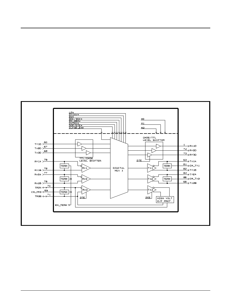
XRT4500
·Á
·Á
·Á
·Á
MULTIPROTOCOL SERIAL NETWORK INTERFACE IC
REV. 1.0.7
40
1.2.1
The "High -Speed Transceiver" Block
The "High-Speed Transceiver" block supports the
transmission and reception of high speed data and
clock signals for the selected "Communication Inter-
face". This block contains receivers RX1 and RX2,
transmitters TX1 and TX2, and bi-directional trans-
ceiver TR3 which is composed of TX3 and RX3. Each
of these devices may be configured to support the
"Electrical Interface" requirements per ITU-T V.35,
ITU-T V.11 (EIA-422), ITU-T V.10 (EIA-423), or ITU-T
V.28 (EIA-232). In the "ITU-T V.35" Mode, each trans-
mitter has a common mode pin that is connected to
the center of the internal termination. This pin should
be bypassed to ground with an external 0.1µF capac-
itor in order to provide the best possible driver output
stage balance.
In a system application, the TX1-RX1 pair and TX2-RX2
pair handle the TXD-RXD (Transmit Data - Receive
Data) and the TXC-RXC (Transmit Clock - Receive
Clock) high speed interface signals respectively. Trans-
ceiver TR3 is dedicated to the SCTE (Transmit Clock
Echo) signal for both DCE and DTE modes of operation.
Transceiver TR3 functions as a receiver for the DTE
mode and as a transmitter during the DCE mode.
F
IGURE
12. H
IGH
-S
PEED
T
RANSCEIVER
B
LOCK

·Á
·Á
·Á
·Á
XRT4500
MULTIPROTOCOL SERIAL NETWORK INTERFACE IC
REV. 1.0.7
41
1.2.2
The "Handshaking/Control Signal Trans-
ceiver" Block
The "Handshaking/Control Signal Transceiver" Block
contains receivers RX4 and RX5, transmitters TX4
and TX5, and a transceiver TR6 which is composed
of TX6 and RX6. Each of these devices may be con-
figured to support the "Electrical Interface" require-
ments per ITU-T V.11 (EIA-422), ITU-T V.10 (EIA-
423), or ITU-T V.28 (EIA-232). The RX4-TX4 pair is
dedicated for the "RTS" (Request to Send) and "CTS"
(Clear-to-Send) signals while RX5-TX5 are intended
to support the "DTR" (Data Terminal Ready) and the
"DSR" (Data Set Ready) signals. Transceiver TR6
supports the "DCD" (Data Carrier Detect) signal.
F
IGURE
13. H
ANDSHAKING
/C
ONTROL
T
RANSCEIVER
B
LOCK

XRT4500
·Á
·Á
·Á
·Á
MULTIPROTOCOL SERIAL NETWORK INTERFACE IC
REV. 1.0.7
42
1.2.3
The "Diagnostic Operation Indicator
Transceiver" Block
The "Diagnostic Operation Indicator Transceiver"
block contains transceiver TR7, which is composed of
TX7 and RX7, receiver RX8 and transmitter TX8.
These devices may be configured to support the
"Electrical Interface" requirements, per ITU-T V.10
(EIA-423) or ITU-T V.28 (EIA-232). These devices
were specifically designed to support the Local Lock
(LL), Remote Loopback (RL) and RI (or TM) signals.
F
IGURE
14. D
IAGNOSTIC
O
PERATION
INDICATOR
T
RANSCEIVER
B
LOCK

·Á
·Á
·Á
·Á
XRT4500
MULTIPROTOCOL SERIAL NETWORK INTERFACE IC
REV. 1.0.7
43
1.3
T
HE
C
ONTROL
B
LOCK
The purpose of the Control Block is to permit the user
to configure the XRT4500 into a wide variety of oper-
ating modes. In particular, the Control Block permits
the user to implement the following configuration se-
lections for the XRT4500.
To select which Communication Interface Mode the
XRT4500 will operate in.
∑ To configure the XRT4500 to operate in either the
DTE or the DCE Mode.
∑ To optionally configure the XRT4500 to operate in a
Loop-back Mode.
∑ To enable or disable the "Echo-Clock" Mode.
∑ To optionally configure the XRT4500 to operate in
the "Latch" Mode.
∑ To optionally configure the XRT4500 to operate in
the "Register" Mode.
∑ To configure the XRT4500 to operate in either the
"2 Clock" or the "3-Clock" Mode.
∑ To enable or disable the Internal Oscillator (for DTE
Stand-Alone Diagnostic operation).
∑ To invert the TXC clock signal (for DCE applica-
tions) or the RXC clock signal (for DTE applica-
tions).
∑ To invert the TXD data (for DCE applications) or the
RXD data (for DTE applications).
The input pins shown in Figure 15, the Control Block,
are described in detail, below.
F
IGURE
15. D
IAGRAM
OF
THE
XRT4500 C
ONTROL
B
LOCK

XRT4500
·Á
·Á
·Á
·Á
MULTIPROTOCOL SERIAL NETWORK INTERFACE IC
REV. 1.0.7
44
1.3.1
M[2:0] - The (Communication Interface)
Mode Control Select Pins.
As mentioned earlier, the XRT4500 is capable of sup-
porting each of the following "Communication Inter-
face" standards.
∑ ITU-T V.35
∑ ITU-T V.28 (EIA-232)
∑ EIA-449
∑ ITU-T V.36
∑ ITU-T X.21
∑ EIA-530
∑ EIA-530(A)
The XRT4500 can be configured to operate in either
one of these "Communication Interface" standards, by
setting the "M[2:0]" bit-fields to the appropriate val-
ues, as listed in Table 5.
N
OTE
: The M[2:0] input pins are internally pulled "high". As
a consequence, the XRT4500 will automatically be config-
ured into the "POWER-DOWN" Mode, if the M[2:0] input
pins are left "floating".
T
ABLE
5: T
HE
R
ELATIONSHIP
BETWEEN
THE
SETTINGS
FOR
THE
M[2:0]
BIT
-
FIELDS
AND
THE
C
ORRESPONDING
C
OMMUNICATION
I
NTERFACE
THAT
IS
SUPPORTED
C
OMMUNICATION
I
NTERFACE
M2
M1
M0
C
OMMENTS
RS423 (V.10)
0
0
0
All Transmitters and Receivers are functioning in the V.10 Mode.
N
OTE
: This is not a standard Communication Interface.
EIA-530A (V.11)
0
0
1
EIA-530 (V.36)
0
1
0
RS449
0
1
0
X.21
0
1
1
V.35
1
0
0
Reserved
1
0
1
RS232 (V.28)
1
1
0
Power Down Mode
1
1
1
All Transmitters and Receivers are shut-off. Transmitter outputs are tri-stated
and all internal loads are disconnected. The charge pump and DC-DC con-
nect continues to operate.

·Á
·Á
·Á
·Á
XRT4500
MULTIPROTOCOL SERIAL NETWORK INTERFACE IC
REV. 1.0.7
45
1.3.2
DCE/DTE - The DCE/DTE Mode Select Pin
The XRT4500 is capable of supporting either the
"DCE" or "DTE" Modes of operation. Setting this in-
put pin "high" configures the XRT4500 to operate in
the "DCE" Mode. Conversely, setting this input pin
"low" configures the XRT4500 to operate in the "DTE"
Mode. A brief description of DCE Mode and DTE
Mode operations are listed below.
Figure 16 presents a very simple illustration of a DCE
Terminal being interfaced to a DTE Terminal. From
this figure, one can make the following observations
about the DCE and DTE Terminals.
The DCE Terminal
The DCE Terminal is responsible for sourcing/gener-
ating all of the following signals.
∑ RXD - Receive Data (High Speed Signal)
∑ RXC - Receive Clock (High Speed Signal)
∑ TXC - Transmit Clock (High Speed Signal)
∑ DSR - Data Set Ready
∑ DCD - Data Carrier Detect
∑ CTS - Clear to Send
∑ RI (Ring Indicator) or
∑ TM (Test Mode).
Further, the DCE Terminal is responsible for receiving/
terminating all of the following signals.
∑ TXD - Transmit Data (High Speed Signal)
∑ TXCE (or SCTE) - Transmit Clock Echo (High
Speed Signal)
∑ DTR - Data Terminal Ready
∑ RTS - Request to Send
∑ LL - Local Loop-back Indicator
∑ RL - Remote Loop-back Indicator
Because of this, whenever the XRT4500 is configured
to operate in the "DCE" Mode, then the following con-
figuration conditions are "TRUE".
∑ Three "high-speed" Transmitters are enabled, and
∑ Two "high-speed" Receivers are enabled.
∑ Four "low-speed" Transmitters are enabled, and
∑ Four "low-speed" Receivers are enabled.
F
IGURE
16. A S
IMPLE
I
LLUSTRATION
OF
THE
DCE/DTE I
NTERFACE
TXD
TXC
RXD
RXC
TXCE
DTR
DSR
DCD
CTS
RTS
LL
RL
RI (or TM)
DTE
EQUIPMENT
DCE
EQUIPMENT
XRT4500
XRT4500
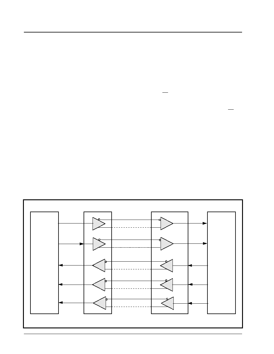
XRT4500
·Á
·Á
·Á
·Á
MULTIPROTOCOL SERIAL NETWORK INTERFACE IC
REV. 1.0.7
46
The DTE Terminal
The DTE Terminal is responsible for sourcing/gener-
ating all of the following signals.
∑ TXD - Transmit Data
∑ TXCE (or SCTE) - Transmit Clock Echo
∑ DTR - Data Terminal Ready
∑ RTS - Request to Send
∑ LL - Local Loop-back Indicator
∑ RL - Remote Loop-back Indicator
Further, the DTE Terminal is responsible for receiv-
ing/terminating all of the following signals.
∑ RXD - Receive Data
∑ TXC - Transmit Clock
∑ RXC - Receive Clock
∑ DSR - Data Set Ready
∑ DCD - Data Carrier Detect
∑ CTS - Clear-to-Send
∑ RI (Ring Indicator)
∑ TM (Test Mode Indicator).
Because of this, whenever the XRT4500 is configured
to operate in the "DTE" Mode, then the following con-
figuration conditions are "TRUE".
∑ Two "high-speed" Transmitters are enabled, and
∑ Three "high-speed" Receivers are enabled.
∑ Four "low-speed" Transmitters are enabled, and
∑ Four "low-speed" Receivers are enabled.
Other Comments about DCE and DTE Equipment
Whenever DCE and DTE Equipment are interfaced to
each other, the DCE Equipment is typically the
source of all timing signals. The DTE Equipment will
typically function as a "Clock Slave".
1.3.3
The LP - Loop-Back Enable/Disable
Select Pin
As mentioned earlier, the XRT4500 can be configured
to operate in the loop-back mode. Setting the "LP" in-
put pin "high" disables the loop-back mode (within the
XRT4500). Conversely, setting this input "low" config-
ures the XRT4500 to operate in the "TXD/RXD" loop-
back mode.
A detailed description of the "TXD/RXD" loop-back
Mode is presented below.
Behavior of DTE/DCE Mode Devices, when the
Loop-Back Mode is Disabled
Figure 17 presents an illustration of a DTE and DCE
Terminal interfaced to each other when no XRT4500
Loop-Back Mode has een configured.
F
IGURE
17. I
LLUSTRATION
OF
BOTH
THE
DTE
AND
DCE M
ODE
XRT4500
OPERATING
,
WHEN
THE
L
OOP
-B
ACK
M
ODE
IS
DISABLED
DTE (#2)
SCC (L)
XRT4500
XRT4500
RX1
TX1
RX2
TX2
RX3
TX3
RX2
TX2
RX1
TX1
RXD
RXC
TXC
SCTE_IN
TXD_IN
TXD
SCTE
TXC_IN
RXC_IN
RXD_IN
60
67
73
74
1
78
79
77
76
70
71
64
65
63
62
1
74
68
67
60
63
62
64
65
70
71
77
76
78
79
TXD
TXC
RXC
RXD
SCC (R)
DTE (#1)*
SCTE
* Indicates scenario # from Table 8

·Á
·Á
·Á
·Á
XRT4500
MULTIPROTOCOL SERIAL NETWORK INTERFACE IC
REV. 1.0.7
47
Figure 27 indicates that the DTE Serial Communica-
tions Controller (SCC) sources the "TXD" signal. This
digital signal is then converted into an "Analog Line"
signal (as dictated by the "M[2:0]" settings) by the
"DTE Mode" XRT4500. This line signal is then trans-
mitted over the DTE/DCE Interface and is received by
the DCE Terminal. This Analog Line signal is then
converted back into the digital format by the "DCE
Mode" XRT4500. This digital signal is ultimately re-
ceived and terminated by the DCE SCC (Serial Com-
munications Controller). Likewise, this figure indicates
that the RXD signal is sourced by the DCE SCC. This
digital signal is then converted into an "Analog Line"
signal by the "DCE Mode" XRT4500. This line signal is
then transported over the DCE/DTE Interface and is re-
ceived by the "DTE Mode" XRT4500. This "Analog Line
signal" is then converted back into the digital format by
the "DTE Mode" XRT4500. The XRT4500 then outputs
this signal to the "DTE SCC". This is considered to the
be the "Normal" (Non-loop-back/Diagnostic) Mode of
operation.
N
OTE
: Figure 27 only depicts the "High-Speed" DCE/DTE
Interface signals. The "Low-Speed" control/handshaking
signals are not affected by the loop-back mode.
Behavior of the DTE Mode XRT4500, when the
Loop-Back Mode is Enabled.
Figure 18 presents an illustration of a DTE and a
DCE Terminal interfaced to each other. In this case,
the XRT4500 (associated with the DTE Terminal) has
been configured to operate in the "Loop-back" Mode
N
OTE
: Figure 18 only depicts the "High-Speed" signals.
The "Low-Speed" control/handshaking signals are not
affected by the loop-back mode.
If the Loop-back Mode is configured within the
XRT4500, while it is operating in the DTE Mode, then
the following two (2) loop-back paths will exist.
∑ A Digital/Terminal-Side Loop-back
∑ An Analog/Line-Side Loop-back
Each of these Loop-back paths are described below.
1. The Digital/Terminal Side Loop-back path:
This loop-back path is referred to as a "Digital/Termi-
nal Side" Loop-back, because all signals originate
from and are terminated by the DTE SCC (e.g., the
Terminal Equipment). The signals (from the DTE
SCC) are never converted into the Analog format,
and are not outputted to the line.
The TXD signal (originating from the DTE SCC),
along with the SCTE (Transmit Echo Clock) will be not
be outputted to the DCE Terminal. Instead, this signal
will be loop-back into the "DTE SCC. The "TXD" sig-
nal will ultimately be outputted to the DTE SCC via
the "RXD" output pin of the "DTE Mode" XRT4500.
The SCTE signal will ultimately output the DTE SCC
via the "RXC" output pin of the XRT4500.
N
OTE
: Since the DTE SCC requires the TXC signal (in
order to synthesize the SCTE signal), this loop-back still
permits the TXC signal to pass through to the DTE SCC.
F
IGURE
18. I
LLUSTRATION
OF
THE
B
EHAVIOR
THE
DTE M
ODE
XRT4500,
WHEN
IT
IS
CONFIGURED
TO
OPERATE
IN
THE
L
OOP
-B
ACK
M
ODE
S C C ( R )
S C C ( L )
X R T 4 5 0 0
X R T 4 5 0 0
R X 1
T X 1
R X 2
T X 2
R X 3
T X 3
R X 2
T X 2
R X 1
T X 1
R X D
R X C
T X C
S C T E _ I N
T X D _ I N
T X D
S C T E
T X C _ I N
R X C _ I N
R X D _ I N
6 0
6 7
7 3
7 4
1
7 8
7 9
7 1
7 7
7 0
7 1
6 4
6 5
6 3
6 2
1
7 4
6 8
6 7
6 0
6 3
6 2
6 4
6 5
7 0
7 1
7 7
7 6
7 8
7 9
T X D
S C T E
T X C
R X C
R X D
Digital/Terminal
Loop-back Path
Analog/Line
Loop-back Path
M U X 1
D C E ( # 2 )
D T E ( # 3 )
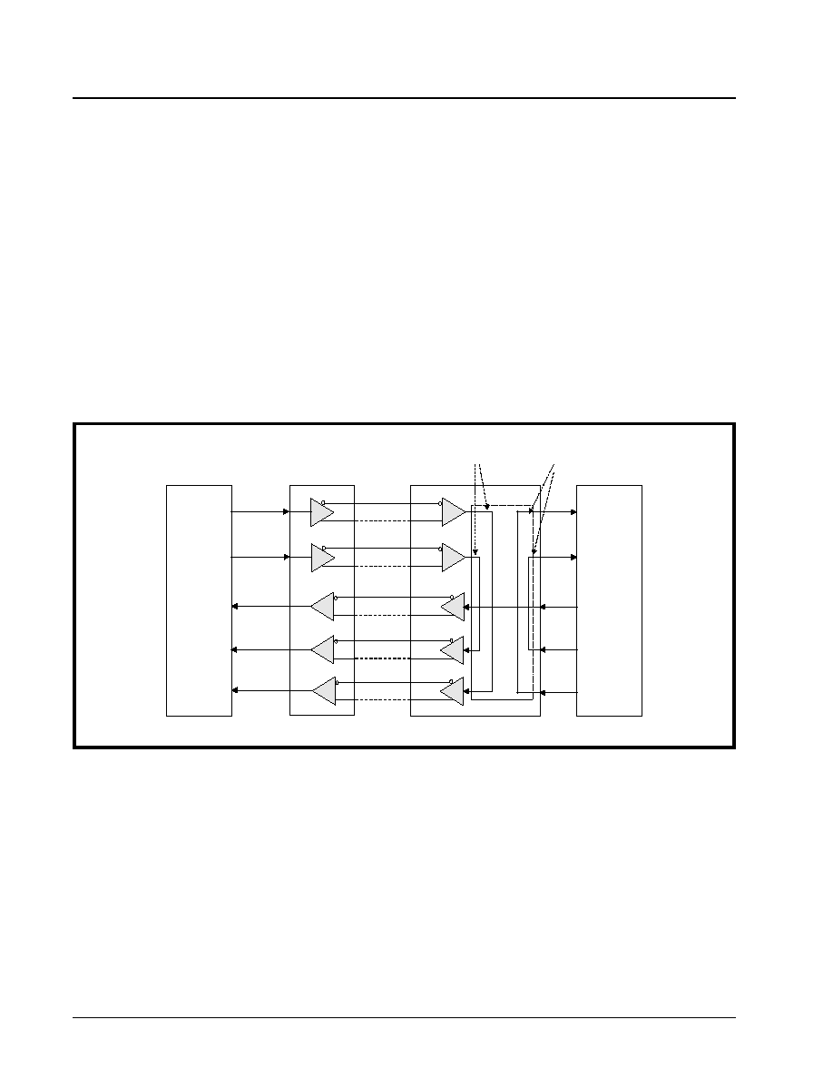
XRT4500
·Á
·Á
·Á
·Á
MULTIPROTOCOL SERIAL NETWORK INTERFACE IC
REV. 1.0.7
48
2. The Analog/Line-Side Loop-back path:
This loop-back path is referred to as an "Analog/Line-
Side" Loop-back, because all signals originate from and
are ultimately terminated by the DCE Terminal. These
signals originate from the DCE Terminal; and are out-
putted to the line, to the DTE Terminal. However, these
signals (from the DCE Terminal) are never converted in-
to the Digital format (by the DTE Mode XRT4500).
These signal are kept in the "Analog" format, and are
looped-back (over the line) to the DCE Terminal.
The RXD signal (originating from the DCE Terminal)
will be transmitted over the line to the DTE Terminal.
However, this signal will not be converted into the dig-
ital format by the "DTE Mode" XRT4500. Instead, this
signal will be looped-back out to the "DCE Terminal"
via the "TXD" signal path.
N
OTE
: In this loop-back mode, the RXC signal (e.g., the
companion clock signal to RXD) is also received by the
DTE Terminal and looped-back out to the DCE Terminal. In
this case, the "RXC" (Receive Clock) signal will be routed to
the DCE Terminal through the "SCTE" signal path The DCE
SCC can still use the RXC (via the SCTE signal path), in
order to sample the RXD signal (which is available via the
"TXD" signal path).
Behavior of the DCE Mode XRT4500, when the
Loop-Back Mode is Enabled.
Figure 19 presents an illustration of a DTE and a
DCE Terminal interfaced to each other. In this case,
the XRT4500 (associated with the DCE Terminal) has
been configured to operate in the "Loop-back" Mode.
N
OTE
: Figure 19 only depicts the "High-Speed" DCE/DTE
Interface signals. The "Low-Speed" control/handshaking
signals are not affected by the loop-back mode.
If the Loop-back Mode is configured within the
XRT4500, while it is operating in the DCE Mode, then
the following two (2) loop-back paths exists.
∑ A Digital/Terminal-Side Loop-back
∑ An Analog/Line-Side Loop-back
Each of these Loop-back paths are described below.
1. The Digital/Terminal Side Loop-back:
Again, this loop-back path is referred to as a "Digital/
Terminal Side" Loop-back, because all of the signals
originate from, and are terminated by the DCE SCC
(e.g., the Terminal Equipment). The signals (originat-
ing at the DCE SCC) are not converted into the Ana-
log format, and are not output to the line.
The "RXD" signal (originating from the DCE SCC)
along with the "RXC" (Receive Clock) signal will not
be converted into the Analog format, nor output to the
DTE Terminal (over the line). Instead, this signal will
remain in the "Digital-format" and will be looped-back
into the DCE SCC. The "RXD" signal will ultimately be
output to the DCE SCC via the "TXD" output of the
"DCE Mode" XRT4500.
N
OTE
: The "RXC" signal (e.g., the companion clock signal to
"RXD") will also be loop-back into the "DCE SCC". This signal
will be output (by the XRT4500) via the "SCTE" output pin.
F
IGURE
19. I
LLUSTRATION
OF
THE
B
EHAVIOR
OF
THE
DCE M
ODE
XRT4500,
WHEN
IT
IS
CONFIGURED
TO
OPERATE
IN
THE
L
OOP
-
BACK
M
ODE
S C C ( R )
S C C ( L )
X R T 4 5 0 0
X R T 4 5 0 0
R X 1
T X 1
R X 2
T X 2
R X 3
T X 3
R X 2
T X 2
R X 1
T X 1
R X D
R X C
T X C
S C T E _ I N
T X D _ I N
T X D
S C T E
T X C _ I N
R X C _ I N
R X D _ I N
6 0
6 7
7 3
7 4
1
7 8
7 9
7 7
7 6
7 0
7 1
6 4
6 5
6 3
6 2
1
7 4
6 8
6 7
6 0
6 3
6 2
6 4
6 5
7 0
7 1
7 7
7 6
7 8
7 9
T X D
S C T E
T X C
R X C
R X D
Analog/Line
Loop-back Path
Digital/Terminal
Loop-back Path
DTE (#1)
DCE (#4)
M U X 1
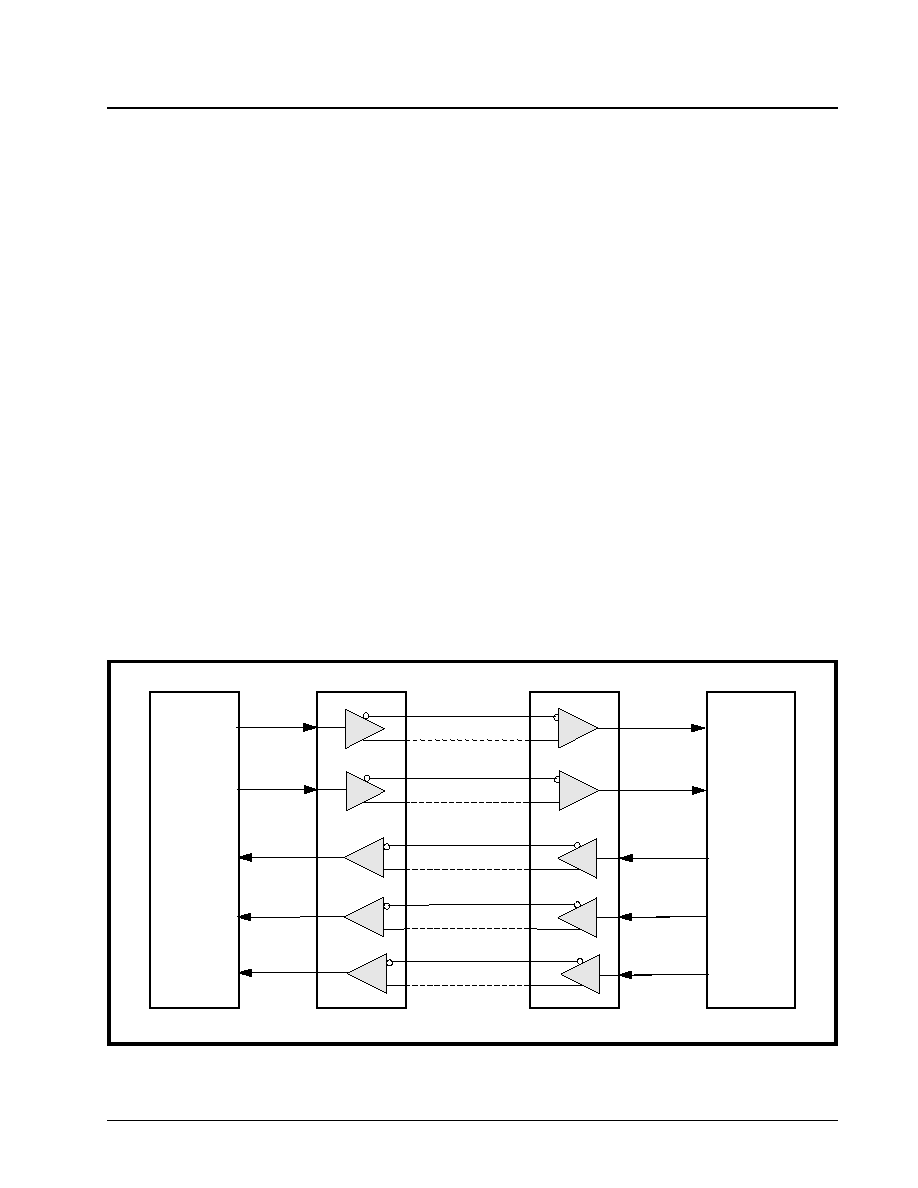
·Á
·Á
·Á
·Á
XRT4500
MULTIPROTOCOL SERIAL NETWORK INTERFACE IC
REV. 1.0.7
49
2. The Analog/Line-Side Loop-back:
This loop-back path is referred to as an "Analog/Line-
Side" loop-back, because all signals originate from
and are terminated by the DTE Terminal (over the
line). These signals originate from the DTE Terminal,
and are output, over the line, to the DTE Terminal.
However, these signal (originating from the DTE Ter-
minal) are never converted into the Digital format (by
the DCE Mode XRT4500). These signals are kept in
the "Analog" format, and are looped-back (over the
line) to the DTE Terminal.
The "TXD" signal (originating from the DTE Terminal)
will be transmitted over the line to the DCE Terminal.
However, this signal will not be converted into the dig-
ital format by the "DCE Mode" XRT4500. Instead, this
signal will be loop-back to the DTE Terminal, via the
"RXD" signal path.
N
OTE
: In this loop-back mode, the "SCTE" signal (e.g., the
companion clock signal to "TXD") is also received by the
DCE Terminal and is looped-back to the DTE Terminal. In
this case, the SCTE signal will be routed through the "RXC"
path. The DTE SCC can use this signal to sample the TXD
(now RXD signal).
1.3.4
The EC* (Echo Clock Mode - Enable/
Disable Select Input pin)
A wide variety of Serial Communications Controller
(SCCs) are deployed in either "DTE" or "DCE" type of
Data Communications equipment. These SCCs can
be realized in an ASIC solution or they can be a stan-
dard product. An example of a standard product SCC,
would be the Am85C30 from AMD.
One variation that exists among these SCCs are in
the number of "Clock Signals" that these chips use
and process, in order to support Data Communica-
tions over a DTE/DCE Interface. For example, some
SCCs process 3 clock signals in order to support the
transmission/reception of data over a DTE/DCE Inter-
face. Other SCCs process only 2 or 1 clock signals.
Examples of a "3-Clock" and a "2-Clock" DTE/DCE
Interface are presented below.
The "3-Clock" DCE/DTE Interface
Many of the Data Communication Standards (e.g.,
ITU-T V.35, EIA-530(A), etc.) define three clock sig-
nals that are to be transported over the DTE/DCE In-
terface. These tree clock signals are listed below.
∑ TXC - Transmit Clock
∑ RXC - Receive Clock
∑ SCTE (or TXCE) - Transmit Clock Echo
Figure 20 presents an illustration of a DTE and DCE
exchanging data over a "3-Clock DTE/DCE" Interface.
F
IGURE
20. I
LLUSTRATION
OF
A
TYPICAL
"3-C
LOCK
DCE/DTE" I
NTERFACE
SCC (R)
SCC (L)
X R T 4 5 0 0
X R T 4 5 0 0
R X D
R X C
T X C
S C T E _ I N
T X D _ I N
T X D
S C T E
T X C _ I N
R X C _ I N
R X D _ I N
6 0
6 7
7 3
2
7 4
1
7 8
7 9
7 7
7 6
7 0
7 1
6 4
6 5
6 3
6 2
1
7 4
6 8
6 7
6 0
6 3
6 2
6 4
6 5
7 0
7 1
7 7
7 6
7 8
7 9
T X D
S C T E
T X C
R X C
R X D
D T E ( # 1 )
D C E ( # 2 )
T X 1
R X 1
R X 2
T X 3
T X 2
T X 1
R X 2
R X 3
T X 2
R X 1
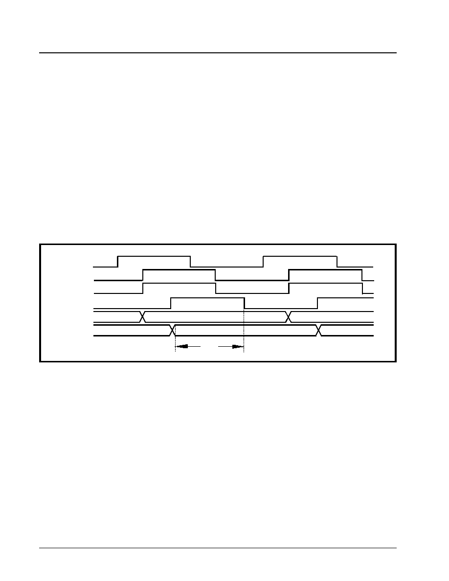
XRT4500
·Á
·Á
·Á
·Á
MULTIPROTOCOL SERIAL NETWORK INTERFACE IC
REV. 1.0.7
50
The important things to note about Figure 20 are as
follows.
1. The DCE Terminal is the ultimate source of all
clock signals.
2. The DCE Serial Communications Controller (SCC)
will transmit the TXC clock signal to the DTE node.
3. The DTE SCC will update the state on the TXD
line, upon the rising edge of the "incoming" TXC clock
signal when `Clock Invert' is not activated.
4. The DTE SCC will generate the rising edge of the
SCTE clock signal, upon receipt of the rising edge of
the "incoming" TXC clock signal when clock invert is
not activated.
5. The DCE SCC will use the falling edge of the
SCTE clock signal in order to sample the "incoming"
TXD signal.
6. Because the DTE provides the SCTE clock signals
and since the falling edge of this clock signal will oc-
cur at the middle of the bit-period (for the signal on
the TXD line); the "3-Clock DTE/DCE Interface" is
largely immune to the affects of propagation delay
(via the DCE SCC to DTE SCC" link and the "DTE
SCC to DCE SCC" link), and will operate properly
over a very wide range of data rates.
Figure 21 presents an illustration of the wave-forms of
the signals that are transported across a "3-Clock
DTE/DCE" Interface. Further, this figure indicates that
a "3-Clock DTE/DCE" Interface provides the DCE
SCC with a TXD to TXC set-up time of "one-half" of
the bit-period (0.5 * tb). Hence, a "3-Clock DTE/DCE"
Interface can support very wide range of data rates,
and still insure that the DCE SCC will be provided a
sufficient "TXD to TXC" set-up time.
The "2-Clock" DTE/DCE Interface
Although the Data Communications standards rec-
ommends the use of these three clock signals; in
practice, some Data Communications Equipment
manufacturers will build equipment that only supports
the transmission of "2-Clock" signals. The reason for
this can be due to cost, or due to the fact that the Da-
ta Communications Equipment manufacturer is using
an SCC that only handles 2-clock signals. When Data
Communications Equipment Manufacturers design
their DCE or DTE equipment to only support the
transmission of two clocks over the DTE/DCE Inter-
face; these two clocks signals are typically the "TXC"
(Transmit Clock) and the "RXC" (Receive Clock) sig-
nals. Figure 22 presents an illustration of a DTE and
DCE exchanging data over a "2-Clock DCE/DTE" In-
terface.
N
OTE
: In the "2-Clock DTE/DCE" Interface, the DTE Termi-
nal does not supply the SCTE clock signal back to the DCE.
F
IGURE
21. I
LLUSTRATION
OF
THE
WAVE
-
FORMS
OF
THE
SIGNALS
THAT
ARE
TRANSPORTED
ACROSS
A
"3-C
LOCK
DTE/DCE" I
NTERFACE
T X C ( a t D C E )
T X C ( a t D T E )
T X D ( a t D T E )
T X D ( a t D C E )
0.5*tb
S C T E ( a t D T E )
S C T E ( a t D C E )
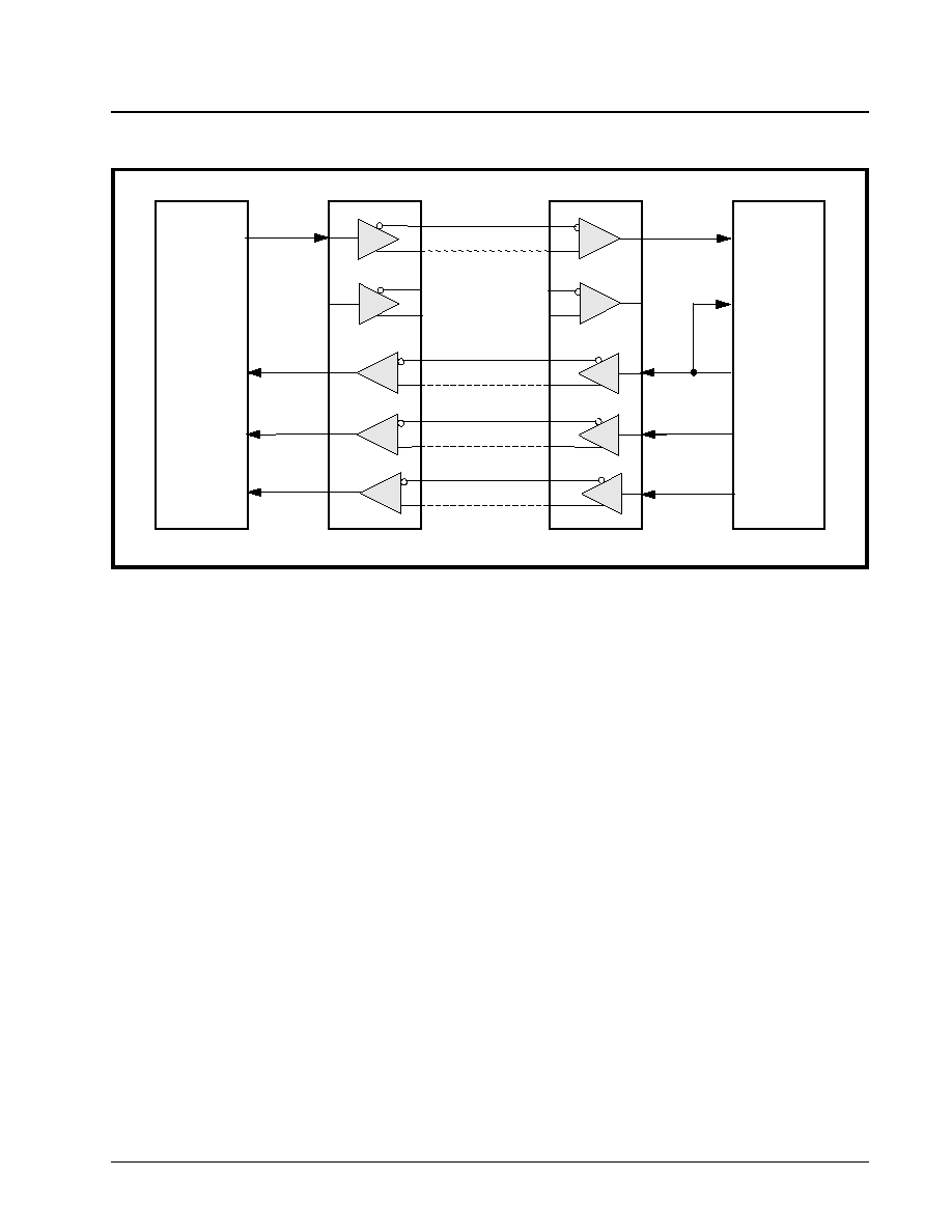
·Á
·Á
·Á
·Á
XRT4500
MULTIPROTOCOL SERIAL NETWORK INTERFACE IC
REV. 1.0.7
51
Since the DTE SCC will not provide the DCE SCC
with the SCTE signal, the DCE SCC will have to use
a different clock signal in order to sample the "incom-
ing" data on the TXD line. A common approach, in
this case, is to simply "hard-wire" the "TXC" output
signal to the "SCTE" input pin of the DCE SCC) and
to use the falling edge of the TXC clock signal in order
to sample the "incoming" data on the TXD line, as il-
lustrated above in Figure 1.8.
N
OTE
: There are numerous bad things about designing
DCE Equipment, per the illustration in Figure 1.9. In addi-
tion to the reasons presented below, since the DCE SCC is
now "hard-wired" to use the "TXC" as the means to sample
the "incoming" "TXD" signal, this approach is not flexible if
the user is interfacing to a DTE that happens to support "3-
Clock" signal. In this case, the user is advised to consider
using the "2-Clock" Mode feature (which is also offered by
the XRT4500) and is discussed in Section 1.2.5.
Important things to note about Figure 1.9.
1. The DTE SCC will not supply the SCTE signal to
the DCE SCC.
2. The DCE SCC will use the falling edge of the (lo-
cally generated) TXC clock signal in order to sample
the "incoming" TXD signal.
Unlike the "3-Clock DTE/DCE" Interface, the "2-Clock
DTE/DCE" Interface is sensitive to the "round-trip"
propagation delay between the DCE and the DTE
Terminals (due to the cable, components comprising
the DCE and DTE Terminals, etc.) An example of this
sensitivity is presented below.
Case 1 - "2-Clock DTE/DCE" Operation at
1.0Mbps
Consider the case where the DCE and DTE are ex-
changing data at a rate of 1.0Mbps. Further, let's con-
sider that the total propagation delay from the DCE to
the DTE is 160 ns. Likewise, let's consider that the to-
tal propagation delay from the DTE to the DCE is also
160ns. Given these conditions, Figure 23 plots out
the clock and signal wave-forms for the TXC and TXD
at both the DCE and DTE SCCs.
F
IGURE
22. I
LLUSTRATION
OF
A
"2-C
LOCK
DTE/DCE" I
NTERFACE
2
SCC (R)
SCC (L)
X R T 4 5 0 0
X R T 4 5 0 0
R X 1
T X 2
R X D
R X C
T X C
S C T E _ I N
T X D _ I N
T X D
S C T E
T X C _ I N
R X C _ I N
R X D _ I N
6 0
6 7
7 3
7 4
1
7 8
7 9
7 7
7 6
7 0
7 1
6 4
6 5
6 3
6 2
1
7 4
6 8
6 7
6 0
6 3
6 2
6 4
6 5
7 0
7 1
7 7
7 6
7 8
7 9
T X D
T X C
R X C
R X D
D C E
D T E
T X 1
R X 3
R X 2
R X 1
R X 2
T X 3
T X 2
T X 1
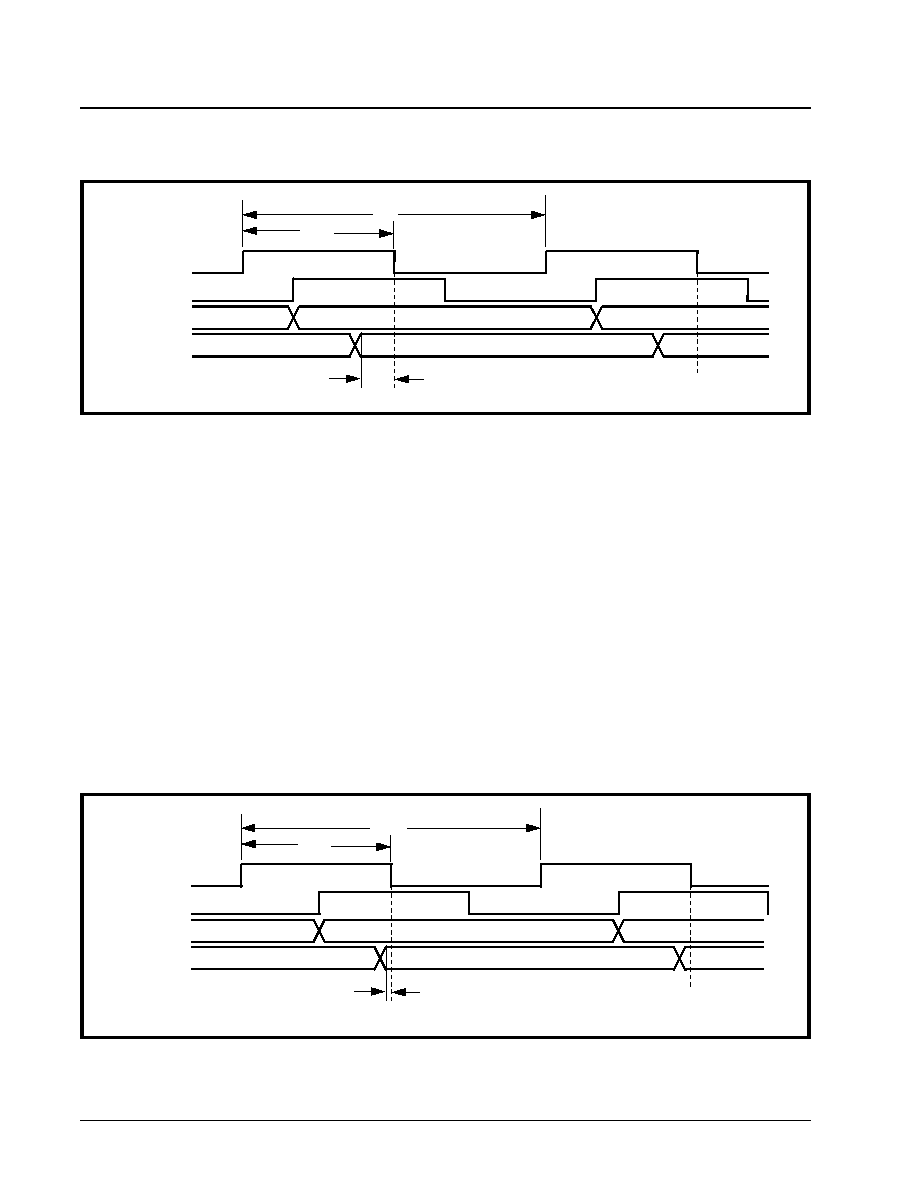
XRT4500
·Á
·Á
·Á
·Á
MULTIPROTOCOL SERIAL NETWORK INTERFACE IC
REV. 1.0.7
52
Figure 23 indicates that the TXC (Transmit Clock) sig-
nal will originate at the DCE SCC terminal. However,
because of the "DCE-to-DTE" propagation delay, the
TXC signal will arrive at the DTE SCC 160ns later.
Per the various "Communication Interface Standards"
(e.g., EIA-530A, etc.), the DTE must update the data
on the "TXD" line upon detection of the rising edge of
the "incoming" TXC clock signal. Hence, Figure 1.10
illustrates the DTE SCC toggling the TXD line coinci-
dent with the rising edge of TXC. Finally, because of
the "DTE to DCE" propagation delay, the TXD signal
will arrive at the DCE SCC 160 ns later.
Recall that the DCE SCC is using the TXC clock sig-
nal to sample the data on the "incoming" TXD line.
The scenario depicted in Figure 1.10 indicates that if
the Data Rate (between the DCE and DTE) is
1.0Mbps; and that if the "DCE to DTE" and "DTE to
DCE" propagation delays are each 160ns, then the
DCE SCC will be provided with 180ns of set-up time,
(in the TXD line) prior to sampling the data. For most
digital IC's, this amount of set-up time is sufficient
long and should not result in any bit errors.
Case 2 - "2 Clock DCE/DTE" Operation at 1.544
Mbps
Now let's consider the case where the DCE and DTE
Terminals are now exchanging data at a rate of
1.544Mbps (e.g., the DS1 rate). Further, let's consid-
er that the "DCE-to-DTE" and "DTE-to-DCE" propa-
gation delays are each 160ns (as in the prior case).
Given these conditions, Figure 24 illustrates the re-
sulting clock and signal wave-forms for the TXC and
TXD at both the DCE and DTE SCCs.
The scenario depicted in Figure 24 indicates that if
the Data Rate (between the DCE and the DTE) is
1.544Mbps and that if the "DCE-to-DTE" and the
"DTE-to-DCE" propagation delays are each 160ns,
then the DCE SCC will be provided with 4ns of set-up
time (in the TXD line) prior to sample the data. For
F
IGURE
23. T
HE
B
EHAVIOR
OF
THE
TXC
AND
TXD S
IGNALS
AT
THE
DCE
AND
DTE SCC
S
, (D
ATA
R
ATE
=
1.0M
BPS
, "DCE-
TO
-DTE"
PROPAGATION
DELAY
= 160
NS
, "DTE-
TO
-DCE"
PROPAGATION
DELAY
= 160
NS
)
TXC (at DCE)
TXD (at DTE)
TXC (at DTE)
TXD (at DCE)
1us
500ns
180ns
F
IGURE
24. T
HE
B
EHAVIOR
OF
THE
TXC
AND
TXD S
IGNALS
AT
THE
DCE
AND
DTE SCC
S
(D
ATA
R
ATE
=
1.544M
BPS
, DCE-
TO
-DTE P
ROPAGATION
D
ELAY
= 160
NS
, DTE-
TO
-DCE P
ROPAGATION
D
ELAY
= 160
NS
)
TXC (at DCE)
TXD (at DTE)
TXC (at DTE)
TXD (at DCE)
648ns
324 ns
4ns

·Á
·Á
·Á
·Á
XRT4500
MULTIPROTOCOL SERIAL NETWORK INTERFACE IC
REV. 1.0.7
53
some digital Is, this amount of set-up time is marginal
and is likely to result in bit-errors. Throughout the re-
mainder of this document, this phenomenon will be
referred to as the "2-Clock/Propagation Delay" phe-
nomenon.
Cases 1 and 2 indicate that if a wide range of data
rates are to be supported by some Data Communica-
tion Equipment over a "2-Clock DTE/DCE" Interface'
and if the propagation delays are sufficiently large (in
the "DCE-to-DTE" and "DTE-to-DCE" link); then there
are some data rates that will be handled in an "error-
free" manner; and other data rates which are prone to
errors. Consequently, the "3-Clock DTE/DCE Inter-
face" is a much more robust and reliable medium to
transport data, than is the "2-Clock DTE/DCE" Inter-
face.
Using the "Echo-Clock" Feature within the
XRT4500
The "Echo-Clock" features within the XRT4500 helps
to mitigate the "2-Clock/Propagation Delay" phenom-
enon by forcing the DTE Mode XRT4500 to supply an
additional clock signal (over the DTE/DCE Interface),
over and above that provided by the DTE SCC.
Figure 25 presents an illustration of the "Echo Clock"
feature (within the DTE Mode XRT4500) being used.
In the example, presented in Figure 25, the DTE SCC
does not supply the SCTE signal to the DTE/DCE In-
terface (just as in the two previous examples). How-
ever, in this case, the XRT4500 (on the DTE side) has
been configured to operate in the "Echo-Clock" Mode.
While the XRT4500 is operating in this mode, it will
simply take the "incoming" Transmit Clock signal
(TXC) and will "echo" it back to the SCTE input pin of
the DCE SCC. If we were to closely analyzer the
clock signals that are transported across the "DTE/
DCE" Interface, in order to determine the resulting
"TXC to TXD set-up time", we would observe the fol-
lowing.
1. The DCE SCC sources the TXC clock signal to the
DTE node.
2. The DTE SCC will update the state of the TXD line
on the rising edge of the "incoming" TXC clock signal.
3. The "DTE" XRT4500 will "internally" route the
"RX3D" output signal to the TX2D output signal. As a
consequence, the incoming TXC clock signal will be
"echoed" back out to the SCTE input pin of the DCE
SCC.
4. If we neglect the "Clock-to-Output" delay of the
DTE SCC, the DCE SCC will receive the falling edge
of the SCTE clock signal, very close to the middle of
the bit-period of each bit on the TXD line.
This phenomenon is also illustrated below in
Figure 26.
F
IGURE
25. I
LLUSTRATION
OF
THE
"E
CHO
-C
LOCK
" F
EATURE
WITHIN
THE
XRT4500
SCC (R)
SCC (L)
X R T 4 5 0 0
X R T 4 5 0 0
R X 1
T X 2
R X D
R X C
T X C
S C T E _ I N
T X D _ I N
T X D
S C T E
T X C _ I N
R X C _ I N
R X D _ I N
6 0
6 7
7 3
7 4
1
7 8
7 9
7 7
7 6
7 0
7 1
6 4
6 5
6 3
6 2
1
7 4
6 8
6 7
6 0
6 3
6 2
6 4
6 5
7 0
7 1
7 7
7 6
7 8
7 9
T X D
S C T E
T X C
R X C
R X D
D C E
D T E
T X 1
R X 3
R X 2
R X 1
R X 2
T X 3
T X 2
T X 1

XRT4500
·Á
·Á
·Á
·Á
MULTIPROTOCOL SERIAL NETWORK INTERFACE IC
REV. 1.0.7
54
By using the "Echo-Clock" feature, within the
XRT4500, the "Overall System" (comprised of the
DTE and DCE Terminals) is nearly as immune to the
"2-Clock/Propagation Delay" phenomenon, as is the
"3-Clock DTE/DCE Interface"; even though the DTE
SCC only processes two clock signals.
Hence, in short, the purpose of the Echo-Clock Mode
is to provide the "Overall-System" with the SCTE
clock signal, when it is not being supplied by the DTE
SCC. The impact of being able to accomplish this is a
more robust, reliable system performance.
Configuring the Echo-Clock Mode
The user can configure the "Echo-Clock" Mode, with-
in the XRT4500, by pulling the "EC" input pin (pin 34)
"low". Conversely, the user can disable the "Echo-
Clock" Mode by pulling the "EC" input pin "high".
When the "EC" input pin is pulled "low", then the
XRT4500 will internally use the "TXC" digital signal
(which is output, from the DTE Mode XRT4500, via
the RX3D output pin) as the source for the "SCTE" (or
the TX2D) signal.
N
OTE
: The "Echo-Clock" Mode is only available if the
XRT4500 is operating the DTE Mode.
1.3.5
The "2CK/3CK" (2-Clock/3-Clock Mode -
Enable/Disable Select Input pin)
Section 1.3.4 discusses the "Echo-Clock" Mode, and
how it can be used to combat the "2-Clock/Propaga-
tion Delay" phenomenon. The "Echo-Clock" Mode is
an approach that can be used to attack this phenom-
enon, if the XRT4500 is designed into a DTE Equip-
ment. However, if a system manufacturer, of DCE
Equipment, encounters this problem, one is not able
to configure a way out of this phenomenon by en-
abling the "Echo-Clock" Mode. Fortunately, the
XRT4500 does offer the "DCE Equipment" design a
couple of another options which can be used to miti-
gate the "2-Clock/Propagation Delay" phenomenon.
These two features are:
∑ The "2-Clock/3-Clock Mode" Feature
∑ The "Clock Inversion" Feature
This section discusses the "2-Clock/3-Clock" Feature.
As mentioned above, if the DTE/DCE Interface only
consists of two clock signals, (e.g., missing the SCTE
signal), then there will be some data rates at which
the DCE SCC will not be provided with sufficient set-
up time, when sampling the TXD signal.
Figure 27 presents an illustration of two XRT4500 be-
ing implemented in a "DTE/DCE" Interface. In this fig-
ure, the "DCE Mode" XRT4500 has been configured
to operate in the "2-Clock" Mode. When the XRT4500
is configured to operate in the "2-Clock" Mode, then it
will internally use the "TXC" signal as a means to syn-
thesize the "SCTE" clock signal (as depicted below).
F
IGURE
26. I
LLUSTRATION
OF
THE
W
AVE
-
FORMS
,
ACROSS
A
DCE/DTE I
NTERFACE
,
WHEN
THE
E
CHO
-C
LOCK
F
EATURE
(
WITHIN
THE
XRT4500)
IS
USED
AS
DEPICTED
IN
F
IGURE
25
T X C ( a t D C E )
T X C ( a t D T E )
T X D ( a t D T E )
T X D ( a t D C E )
0.5*tb
S C T E ( a t D T E )
S C T E ( a t D C E )

·Á
·Á
·Á
·Á
XRT4500
MULTIPROTOCOL SERIAL NETWORK INTERFACE IC
REV. 1.0.7
55
In this case, the "2-Clock" Mode offers a considerable
amount of design flexibility. This approach permits the
"DCE Equipment" System Design Engineer to design
and layout a board that can be automatically config-
ured to support either the "3-Clock" Mode (if all three
clock signals are present, over the DTE/DCE Inter-
face). Further, this approach also permits the System
Design Engineer to configure the XRT4500 into the
"2-Clock" Mode (if the SCTE clock signal is not
present). This feature is a nice alternative to "hard-
wiring" the "TXC" output (of the DCE SCC) to the
"SCTE" input.
N
OTE
: The "2-Clock" Mode feature, by itself, does not solve
the "2-Clock/Propagation Delay" phenomenon. However,
the "2-Clock" Mode, within the XRT4500, permits the user
to do the following.
a. To configure the XRT4500 to automatically operate
in the "3-Clock" Mode, whenever it is interfaced to a
DTE that supports all three (3) clock signals, or
b. To configure the XRT4500 to automatically operate
in the "2-Clock" Mode, whenever it is interfaced to a
DTE that only supports two (2) clock signals. Once
the user has configured the XRT4500 to operate in
the "2-Clock" Mode, then the user can "solve" the "2-
Clock/Propagation Delay" phenomenon by invoking
the "Clock Inversion" feature, as described below in
Section 1.2.6.
Configuring the "2-Clock" Mode.
The user can configure the XRT4500 to operate in
the "2-Clock" Mode by setting the "2CK/3CK" input
pin "high". Conversely, the user can disable the "2-
Clock" Mode (otherwise known as operating the
XRT4500 in the "3-Clock" Mode) by setting the "2CK/
3CK" input pin "low".
1.3.6
The "Clock Inversion" (CK_INV) feature
The XRT4500 can be configured to invert the "TXC"
signal by setting the "CK_IN" input pin (pin 54) "low".
Setting the "CK_INV" input to "high" removes the in-
vert from the "TXC" signal path. An illustration of the
"DCE Mode" XRT4500, configured to invert the "TXC"
signal is illustrated in Figure 28.
F
IGURE
27. I
LLUSTRATION
OF
THE
DCE/DTE I
NTERFACE
,
WITH
THE
DCE M
ODE
XRT4500
OPERATING
IN
THE
"2-
C
LOCK
" M
ODE
D C E
S C C ( L )
X R T 4 5 0 0
X R T 4 5 0 0
R X 1
T X 1
R X 2
T X 2
R X 3
T X 3
R X 2
T X 2
R X 1
T X 1
R X D
R X C
T X C
S C T E _ I N
T X D _ I N
T X D
S C T E
T X C _ I N
R X C _ I N
R X D _ I N
6 0
6 7
7 3
7 4
1
7 8
7 9
7 7
7 6
7 0
7 1
6 4
6 5
6 3
6 2
1
7 4
6 8
6 7
6 0
6 3
6 2
6 4
6 5
7 0
7 1
7 7
7 6
7 8
7 9
T X D
T X C
R X C
R X D
S C C ( R )
D T E

XRT4500
·Á
·Á
·Á
·Á
MULTIPROTOCOL SERIAL NETWORK INTERFACE IC
REV. 1.0.7
56
The "Clock Inversion" feature is also available if the
XRT4500 is operating in the "DTE" Mode. Figure 29
presents an illustration of a DTE Mode XRT4500,
when it is configured to invert the TXC clock signal.
The Benefits of the "Clock Inversion" Feature
In Section 1.3.4 of this document, a lengthy discussion,
regarding the "2-Clock/Propagation Delay" phenomenon
is presented. In this Section, the "Echo-Clock" Fea-
ture was also presented as a possible solution to the
"2-Clock/Propagation Delay" phenomenon. However,
the "Echo-Clock" feature has a drawback. If a "DCE
Equipment" manufacturer were to interface his/her
equipment to a DTE Terminal that does not support
F
IGURE
28. I
LLUSTRATION
OF
THE
DCE M
ODE
XRT4500
BEING
CONFIGURED
TO
INVERT
THE
TXC
SIGNAL
S C C ( R )
S C C ( L )
X R T 4 5 0 0
X R T 4 5 0 0
R X 1
T X 1
R X 2
T X 2
R X 3
T X 3
R X 2
T X 2
R X 1
T X 1
R X D _ O U T
R X C
T X C
S C T E _ I N
T X D _ I N
T X D
S C T E
T X C _ I N
R X C _ I N
R X D _ I N
6 0
6 7
7 3
7 4
1
7 8
7 9
7 7
7 6
7 0
7 1
6 4
6 5
6 3
6 2
1
7 4
6 8
6 7
6 0
6 3
6 2
6 4
6 5
7 0
7 1
7 7
7 6
7 8
7 9
T X D
S C T E
T X C
R X C
R X D
D C E
D T E
F
IGURE
29. I
LLUSTRATION
OF
THE
DTE M
ODE
XRT4500
BEING
CONFIGURED
TO
INVERT
THE
TXC
SIGNAL
S C C ( R )
S C C ( L )
X R T 4 5 0 0
X R T 4 5 0 0
R X 1
T X 1
R X 2
T X 2
R X 3
T X 3
R X 2
T X 2
R X 1
T X 1
R X D
R X C
T X C
S C T E _ I N
T X D _ I N
T X D
S C T E
T X C _ I N
R X C _ I N
R X D _ I N
6 0
6 7
7 3
7 4
1
7 8
7 9
7 7
7 6
7 0
7 1
6 4
6 5
6 3
6 2
1
7 4
6 8
6 7
6 0
6 3
6 2
6 4
6 5
7 0
7 1
7 7
7 6
7 8
7 9
T X D
S C T E
T X C
R X C
R X D
D C E
D T E

·Á
·Á
·Á
·Á
XRT4500
MULTIPROTOCOL SERIAL NETWORK INTERFACE IC
REV. 1.0.7
57
the SCTE clock signal; it is highly unlikely that the
"DCE Equipment" manufacturer will be able to (over
the DTE/DCE Interface) invoke the "Echo-Clock"
mode and resolve the "2-Clock/Propagation Delay"
phenomenon.
N
OTE
: This is especially the case if the DTE Equipment is
not using the XRT4500 as the Multi-protocol Transceiver IC.
As a consequence, the "DCE Equipment" manufac-
turer would have to resort to undesirable things, such
as using the (locally generated) TXC signal as the
sampling clock for the "TXD" signal.
However, the XRT4500 does offer the DCE Equip-
ment manufacturer an elegant solution to the "2-
Clock/Propagation Delay" phenomenon. By doing the
following things.
a. Configuring the DCE Mode XRT4500 to operate in
the "2-Clock" Mode, and
b. Inverting the TXC signal, within the DCE Mode
XRT4500, the user can largely resolve the "2-Clock/
Propagation Delay" phenomenon.
Figure 30 presents an illustration of the DCE Mode
XRT4500, being configured to (1) operate in the "2-
Clock" Mode, and (2) to invert the "TXC" signal.
By taking advantage of both the "2-Clock" Mode and
the ability to invert the "TXC" clock signal, the "DCE
Equipment" manufacture can mitigate the "2-Clock/
Propagation Delay" phenomenon by simply inverting
the "TXC" whenever the DTE/DCE Interface and sys-
tem configuration settings begin to violate the "TXD to
TXC" set-up time requirement of the DCE SCC de-
vice. By inverting the TXC signal, the phase relation-
ship, between the "TXD and the TXC signal will shift
by 180 degrees. At this point, the sampling edge of
the TXC signal will be near the middle of the "TXD"
bit-period, and the system will not be violating the
"TXD to TXC" set-up time requirements of the DCE
SCC device.
In summary, the "2-Clock" Mode (within the
XRT4500) provides the user with the following op-
tions.
The DCE Equipment (which uses the XRT4500) can
easily be configured to interface to DTE Equipment
that supports the SCTE clock signal, as well as DTE
Equipment that does not support the SCTE clock sig-
nal. If the DCE Equipment is being interfaced to a
DTE which supports the SCTE clock signal, then the
DCE Equipment should configure the XRT4500 to op-
erate in the "3-Clock" Mode. Conversely, if the DCE
Equipment is being interfaced to a DTE which does
not support the SCTE clock signal, then the DCE
Equipment should configure the XRT4500 to operate
in the "2-Clock" Mode. This step will automatically
configure the XRT4500 to route the "TXC" clock sig-
F
IGURE
30. I
LLUSTRATION
OF
THE
DCE M
ODE
XRT4500,
WHICH
IS
OPERATING
IN
THE
"2-C
LOCK
" M
ODE
,
AND
INVERTING
THE
"TXC"
SIGNAL
S C C ( R )
S C C ( L )
X R T 4 5 0 0
X R T 4 5 0 0
R X 1
T X 1
R X 2
T X 2
R X 3
T X 3
R X 2
T X 2
R X 1
T X 1
R X D _ O U T
R X C
T X C
S C T E _ I N
T X D _ I N
T X D
S C T E
T X C _ I N
R X C _ I N
R X D _ I N
6 0
6 7
7 3
7 4
1
7 8
7 9
7 7
7 6
7 0
7 1
6 4
6 5
6 3
6 2
1
7 4
6 8
6 7
6 0
6 3
6 2
6 4
6 5
7 0
7 1
7 7
7 6
7 8
7 9
T X D
S C T E
T X C
R X C
R X D
D C E
D T E

XRT4500
·Á
·Á
·Á
·Á
MULTIPROTOCOL SERIAL NETWORK INTERFACE IC
REV. 1.0.7
58
nal to the "SCTE_IN" input pin of the DCE SCC.
There is no need to design in extra glue logic to multi-
plex the "SCTE" output pin of the XRT4500 with the
TXC output pin of the DCE SCC.
Additionally, if the DCE Equipment is being interfaced
to a DTE Terminal which does not support the SCTE
signal, (e.g., the XRT4500 is now operating in the "2-
Clock" Mode), and if the "DCE/DTE Interface" config-
uration settings are such that the "TXD-to-TXC" set-
up time requirements of the DCE SCC are being vio-
lated, then the user can eliminate this problem by in-
voking the "Clock Invert" feature of the XRT4500.
1.3.7
The Latch Mode of Operation
The Latch Mode of operation permits the user to latch
the state of the "Mode Control" input pins (M[2:0]) into
the XRT4500 internal circuitry. This feature frees up
of the signals, driving the M[2:0] input pins (pins 6, 5,
and 4) for other purposes.
Because of this feature, it is permissible to control the
state of the "M[2:0]" input pins via certain signals
within a bi-directional data bus (which is controlled by
a microprocessor or microcontroller).
The user invokes this feature by driving the "LATCH"
input pin (pin 44) from "low" to "high". During this
"low" to "high" transition, the contents of the "M[2:0]"
input pins will be "locked" (or latched) into internal cir-
cuitry within the XRT4500. At this point (as long as
the "LATCH" input pin remains "high") the user's sys-
tem can do other things with the signal which are also
driving the "M[2:0]" without affecting the behavior the
XRT4500.
The user disables the "LATCH" feature by driving the
"LATCH" input pin, from "high" to "low". Once the
"LATCH" input pin is "low", then the behavior of the
XRT4500 will be dictated by the state of the "M[2:0]"
input pins.
1.3.8
The Registered Mode of Operation
The XRT4500 includes a feature which is known as
"Registered Mode" operation. The user can enable
the "Registered" Mode by setting the "REG" input pin
"HIGH". Conversely, the user can disable the "Regis-
tered" Mode by setting the "REG" input pin "LOW".
If the user enables the "Registered" Mode, then the
following things will happen.
a. The XRT4500 will be configured to sample and
latch the contents of the "TX5D" and "TX8D" input
pins, upon the rising edge of the "REG_CLK" input
signal.
b. The XRT4500 will be configured to output data (to
the SCC) via the "RX5D" and "RX8D" output pins, up-
on the rising edge of the "REG_CLK" signal.
This feature is useful in application, which use a SCC
or a Microcontroller (that requires an external clock
signal to sample the "DSR" and the "RI" (or "TM") sig-
nals. Further, this feature also configures the
XRT4500 to sample the state of the "DTR" and the
"RL" signal upon the rising edge of an external clock
signal.
If the user invokes this feature, then the relationship
between the XRT4500 and the SCC/Microprocessor
is as depicted below in Figure 31.
F
IGURE
31. A
N
I
LLUSTRATION
OF
THE
E
FFECTIVE
I
NTERFACE
BETWEEN
THE
XRT4500
AND
THE
SCC/M
ICROPRO
-
CESSOR
WHEN
THE
"R
EGISTERED
" M
ODE
IS
ENABLED
TX5D
RX5D
TX8D
RX8D
REG_CLK
µ
µ
µ
µ
C
/
µ
µ
µ
µ
P
DTR_Signal
DSR_Signal
RL_Signal
RI_Signal
External Clock
XRT4500

·Á
·Á
·Á
·Á
XRT4500
MULTIPROTOCOL SERIAL NETWORK INTERFACE IC
REV. 1.0.7
59
A system design similar to that presented below in
Figure 32, will accomplish the exact same function/re-
lationship between another Multi-protocol Transceiver
IC and the SCC/Microprocessor.
1.3.9
The Internal Oscillator
The XRT4500 includes an "Internal Oscillator" that
can be used to support "DTE Stand-Alone Testing/
Diagnostics" operations.
The user can enable the "Internal Oscillator" feature
(within the XRT4500) by pulling the "OSC_EN" input
pin (pin 53) "low". Conversely, the user can disable
the "Internal Oscillator" feature by pulling the
"OSC_EN" input pin "high".
If the user enables this feature, then the XRT4500 will
synthesize a clock signal (of frequencies ranging from
32kHz to 64kHz). Further, this clock signal will be out-
put via the "RX2D" and the "RX3D" output pins. Fig-
ure 1.20 presents an illustration of the XRT4500
(while interfaced to the DTE SCC) when the Internal
Oscillator is enabled.
F
IGURE
32. A
N
I
LLUSTRATION
OF
THE
N
ECESSARY
G
LUE
L
OGIC
REQUIRED
TO
DESIGN
A
FEATURE
SIMILAR
TO
THAT
OFFERED
BY
THE
"R
EGISTERED
" M
ODE
,
WHEN
USING
A
DIFFERENT
M
ULTI
-
PROTOCOL
S
ERIAL
N
ETWORK
I
NTERFACE
IC
µ C / µ P
Serial
N e t w o r k
Interface Device
D T R _ S i g n a l
D S R _ S i g n a l
R L _ S i g n a l
RI_Signal
D-Flip-Flops
Clock
Q
Q
Q
Q
C L K
C L K
C L K
C L K
Clock Source
D T E M o d e

XRT4500
·Á
·Á
·Á
·Á
MULTIPROTOCOL SERIAL NETWORK INTERFACE IC
REV. 1.0.7
60
If the user enables the Internal Oscillator, within the
XRT4500, then the XRT4500 will output between a
32kHz and a 64kHz clock signal via the RX2D and
RX3D signals. When the XRT4500 is interfaced to the
DTE SCC, this translates into the XRT4500 generating
the timing signals for "TXC" and the "RXC" input signals.
As a consequence, the DTE SCC is provided with all of
the requisite timing signals that it would normally have, if
it were interfaced to a DCE Terminal. This feature per-
mits the user to implement a wide variety of diagnostic
programs for DTE Equipment stand-alone testing.
N
OTE
: The Internal Oscillator feature is only available if the
XRT4500 has been configured to operate in the DTE Mode.
1.3.10 Glitch Filters
Occasional extraneous glitches on control/handshake
signal inputs such as CTS, RTS, DTR and DSR can
have damaging effects on the integrity of a connection.
The XRT4500 is equipped with lowpass filters on the
input of each of the receivers for the control and
handshake signals. These filters eliminate glitches
which are narrower than 10µs. The user may disable
these filters by setting EN_FLTR to logic 0.
1.3.11 Data Inversion
Similar to TXC, there is a provision in the XRT4500 to
invert the TXD and RXD signals. Once the Setting
the DTINV* input to logic 0 enables an inverter at the
output of RX1 and input of TX1.
1.3.12 Data Interlude
Similar to TXC, there is a provision in the XRT4500 to
invert the TXD and RXD signals. Once the Setting the
DTINV* input to logic 0 enables an inverter at the out-
put of RX1 and input of TX1.
2.0
RECEIVER AND TRANSMITTER
SPECIFICATIONS
Table 3 and Table 4, which are for the XRT4500 re-
ceiver and transmitter sections respectively, summa-
rize the electrical requirements for V.35, V.11, V.10,
and RS232 interfaces. These tables provide virtually
all of the electrical information necessary to describe
these 4 interfaces in a concise form.
3.0
V.10\V.28 OUTPUT PULSE RISE AND FALL
TIME CONTROL
SLEW_CNTL (pin 47) is an analog output that con-
trols transmitter pulse rise and fall time for the V.10
and V.28 modes. Connecting a resistor, RSLEW, hav-
ing a value between 0 and 200 k
from this pin to
ground controls the rise/fall times for V.10 and the
slew rate for V.28 as shown in Figure 34 and
Figure 35 respectively.
F
IGURE
33. I
LLUSTRATION
OF
THE
I
NTERNAL
O
SCILLATORS
WITHIN
THE
XRT4500
S C C ( L )
X R T 4 5 0 0
R X 1
R X 2
R X 3
T X 2
T X 1
T X D
S C T E
T X C _ I N
R X C _ I N
R X D _ I N
7 4
7 3
T X D
S C T E
T X C
R X C
R X D
O S C
O S C
O S C
O S C
D T E

·Á
·Á
·Á
·Á
XRT4500
MULTIPROTOCOL SERIAL NETWORK INTERFACE IC
REV. 1.0.7
61
4.0
THE HIGH-SPEED RS232 MODE
F
IGURE
34. V.10 R
ISE
/F
ALL
T
IME
AS
A
F
UNCTION
OF
RSLEW
10K
1
10
100
1 10
3
R (Ohms)
V
.
1
0
Ri
se
/
F
a
ll
Tim
e
(u
s)
100K
1 Meg
F
IGURE
35. V.28 S
LEW
R
ATE
O
VER
± 3 V O
UTPUT
R
ANGE
WITH
3
K
IN
P
ARALLEL
WITH
2500
P
F L
OAD
AS
A
F
UNCTION
OF
RSLEW
10K
100K
1 Meg
0.01
0.1
1
10
R (Ohms)
V.
28
Sle
w
Ra
te
(V/
us)

XRT4500
·Á
·Á
·Á
·Á
MULTIPROTOCOL SERIAL NETWORK INTERFACE IC
REV. 1.0.7
62
When E_232H (pin 55) is set to logic 0 in RS232 mode,
the transmitters are configured to operate in a special
high-speed RS232 mode that can drive loads of 3000
in parallel with 1000pF at speeds up to 256 KHz.
5.0
INTERNAL CABLE TERMINATIONS
XRT4500 has fully integrated receiver and transmitter
cable terminations for high speed signals (RXD, TXD,
RXC, TXC, SCTE). Therefore, no external resistors
and/or switches are necessary to implement the prop-
er line termination. The schematic diagrams given in
Figures 26 and 27 show the effective receiver and
transmitter terminations respectively for each mode of
operation. When a specific electrical interface is se-
lected by M0, M1 and M2, the termination required for
that interface is also automatically chosen. The
XRT4500 eliminates double termination problems
and makes point to midpoint operation possible in the
V.11 mode by providing the option for disabling the in-
ternal input termination on high speed receivers.
6.0
OPERATIONAL SCENARIOS
Visualizing features such as clock/data inversion,
echoed clock, and loopbacks, in DTE and DCE
modes makes configuring the XRT4500 a non-trivial
task. A series of 48 system level application diagrams
located at the end of the data sheet called "Scenari-
os" assist users in understanding the benefits of
these different features. The internal XRT4500 con-
nections required for a particular scenario are made
through MUX1 and MUX2 that are shown on the
block diagrams given in Figures 2 and 3 respectively.
Table 8 contains the signal routing information versus
control input logic level for MUX1 and Table 9 con-
tains similar information for MUX2.
7.0
APPLICATIONS INFORMATION
Traditional interfaces either require different transmit-
ters and receivers for each electrical standard, or use
complicated termination switching methods to change
modes of operation. Mechanical switching schemes,
which are expensive and inconvenient, include relays,
and custom cables with the terminations located in
the connectors. Electrical switching circuits using
FETs are difficult to implement because the FET
must remain off when the signal voltage exceeds the
supply voltage and when the interface power is off.
The XRT4500 uses innovative, patented circuit de-
sign techniques to solve the termination switching
problem. It includes internal circuitry that may be con-
trolled by software to provide the correct terminations
for V.10 (RS423), V.11 (RS422), V.28 (RS232), and
V.35 electrical interfaces. The schematic diagrams
given in Figures 26 and 27 conceptually show the
switching options for the high-speed receiver input
and transmitter output terminations respectively. Ad-
ditionally, Tables 4 and 5 provide a summary of re-
ceiver and transmitter specifications respectively for
the different electrical modes of operation.
V.10 (RS423) Interface
Figure 28 shows a typical V.10 (RS423) interface.
This configuration uses an unbalanced cable to con-
nect the transmitter TXA output to the receiver RXA
input. The "B" outputs and inputs that are present on
the differential transmitters and receivers contained in
the XRT4500 are not used. The system ground pro-
vides the signal return path. The receiver input resis-
tance is 10 k
nominal and no other cable termina-
tion is normally used for the V.10 mode.
V.11 (RS422) Interface
Figure 29 shows a typical V.11 (RS422) interface. This
configuration uses a balanced cable to connect the
transmitter TXA and TXB outputs to the receiver RXA
and RXB inputs respectively. The XRT4500 includes
provisions for adding a 125
terminating resistor for
the V.11 mode. Although this resistor is optional in the
V.11 specification, it is necessary to prevent reflections
that would corrupt signals on high-speed clock and data
lines. The differential receiver input resistance without
the optional termination is 20 k
nominal.
V.28 (RS232) Interface
Figure 28 shows a typical V.28 (RS232) interface.
This configuration uses an unbalanced cable to con-
nect the transmitter TXA output to the receiver RXA
input. The "B" outputs and inputs that are present on
the differential transmitters and receivers contained in
the XRT4500 are not used. The system ground pro-
vides the signal return path. The receiver "B" input is
internally connected to a 1.4 V reference source to
provide a 1.4 V threshold. The receiver input resis-
tance is 5 k
nominal and no other cable termination
is normally used for the V.28 mode.
V.35 Interface
Figure 30 shows a typical V.35 interface. This configu-
ration uses a balanced cable to connect the transmit-
ter TXA and TXB outputs to the receiver RXA and
RXB inputs respectively. The XRT4500 internal termi-
nations meets the following V.35 requirements. The
receiver differential input resistance is 100
± 10
and the shorted-terminal resistance (RXA and RXB
connected together) to ground is 150
± 15
. The
transmitter differential output resistance is 100
± 10
and the shorted-terminal resistance (TXA and TXB
connected together) to ground is 150
± 15
.
The junction of the 3 resistors (CMTX) on the transmit
termination is brought out to pins 61 and 66 for TX1

·Á
·Á
·Á
·Á
XRT4500
MULTIPROTOCOL SERIAL NETWORK INTERFACE IC
REV. 1.0.7
63
and TX2 respectively. Figure 30 shows how capacitor
C having a value of 100 to 1000 pF bypasses this
point to ground to reduce common mode noise. This
capacitor shorts current caused by differential driver
rise and fall time or propagation delay miss-match di-
rectly to ground. If it was not present, the flow of this
current through the 125
resistor to ground would
cause common mode voltage spikes at the TXA and
TXB outputs.
F
IGURE
36. R
ECEIVER
T
ERMINATION
R1
20
S1
RXxA
RXxB
R3
85
R4
30
R6
125
S3
R2
20
S2
R4
30
R8
10K
S4
R10
4K
R11
6K
R9
4K
R12
6K
Rx
T
ABLE
6: R
ECEIVER
S
WITCHES
M
ODE
S
WITCHES
S1
S2
S3
S4
V.35
Closed
Closed
Open
Open
V.11 Terminated
Open
Open
Closed
Open
V.11 Unterminated
Open
Open
Open
Open
V.10
Open
Open
Open
Open
V.28
Open
Open
Open
Closed

XRT4500
·Á
·Á
·Á
·Á
MULTIPROTOCOL SERIAL NETWORK INTERFACE IC
REV. 1.0.7
64
F
IGURE
37. T
RANSMITTER
T
ERMINATION
TXxA
TXxB
S1
R1
50
R3
125
S2
R2
50
TX
T
ABLE
7: T
RANSMITTER
S
WITCHES
M
ODE
S
WITCHES
S1
S2
V.35
Closed
Closed
V.11/V.10/V.28
Open
Open
F
IGURE
38. T
YPICAL
V.10
OR
V.28 I
NTERFACE
(R1 = 10 K
IN
V.10
AND
5 K
IN
V.28)
F
IGURE
39. T
YPICAL
V.11 I
NTERFACE
(T
ERMINATION
R
ESISTOR
, R1,
IS
O
PTIONAL
.)

·Á
·Á
·Á
·Á
XRT4500
MULTIPROTOCOL SERIAL NETWORK INTERFACE IC
REV. 1.0.7
65
N
OTE
: All Resistors shown above are internal to the
XRT4500
F
IGURE
40. T
YPICAL
V.35 I
NTERFACE
0.1uf
T
ABLE
8: MUX1 C
ONNECTION
T
ABLE
S
CENARIO
N
UMBER
L
OGIC
LEVEL
A
PPLIED
TO
C
ONTROL
I
NPUT
N
AME
/P
IN
N
UMBER
S
IGNAL
S
OURCE
FOR
O
UTPUT
N
AME
/P
IN
N
UMBER
DCE/
DTE
31
EC
34
2CK/
3CK
50
LP
18
CK
INV
54
DT
INV
55
EN_O
SC
53
RX1D
1
TX1B-TX1A
62, 63
RX2D
74
TX2B-TX2A
65, 64
RX3D
73
TR3B-TR3A
71, 70
1
0
1
0
1
1
1
1
RX1B-RX1A
TX1D
RX2B-RX2A
TX2D
TR3B-TR3A
X
2
1
1
0
1
1
1
1
RX1B-RX1A
TX1D
RX2B-RX2A
TX2D
X
TX3D
3
0
1
0
0
1
1
1
TX1D
RX1B-RX1A
TX2D
RX2B-RX2A
TR3B-TR3A
X
4
1
1
0
0
1
1
1
TX1D
RX1B-RX1A
TX2D
RX2B-RX2A
X
TX3D
5
0
1
0
1
0
1
1
RX1B-RX1A
TX1D
RX2B-RX2A
TX2D
(TR3B-TR3A)*
X
6
1
1
0
1
0
1
1
RX1B-RX1A
TX1D
RX2B-RX2A
TX2D
X
(TX3D)*
7
0
1
0
0
0
1
1
TX1D
RX1B-RX1A
TX2D
RX2B-RX2A
(TR3B-TR3A)*
X
8
1
1
0
0
0
1
1
TX1D
RX1B-RX1A
TX2D
RX2B-RX2A
X
(TX3D)*
9
0
1
1
1
1
1
1
RX1B-RX1A
TX1D
RX2B-RX2A
X
TR3B-TR3A
X
10
1
1
1
1
1
1
1
RX1B-RX1A
TX1D
TX3D
TX2D
X
TX3D
11
0
1
1
0
1
1
1
TX1D
RX1B-RX1A
TX2D
X
TR3B-TR3A
X
12
1
1
1
0
1
1
1
TX1D
RX1B-RX1A
TX2D
TX3D
X
TX3D
13
0
1
1
1
0
1
1
RX1B-RX1A
TX1D
RX2B-RX2A
X
(TR3B-TR3A)*
X
14
1
1
1
1
0
1
1
RX1B-RX1A
TX1D
TX3D
TX2D
X
(TX3D)*
15
0
1
1
0
0
1
1
TX1D
RX1B-RX1A
TX2D
X
(TR3B-TR3A)*
X
16
1
1
1
0
0
1
1
TX1D
RX1B-RX1A
TX2D
TX3D
X
(TX3D)*
17
0
1
X
1
1
1
1
RX1B-RX1A
TX1D
RX2B-RX2A
X
RX2B-RX2A
X
18
1
1
X
1
1
1
1
RX1B-RX1A
TX1D
TX2D
TX2D
X
X
19
0
1
X
0
1
1
1
TX1D
RX1B-RX1A
TX2D
X
TR3B-TR3A
X
20
1
1
X
0
1
1
1
TX1D
RX1B-RX1A
TX2D
RX2B-RX2A
X
X

XRT4500
·Á
·Á
·Á
·Á
MULTIPROTOCOL SERIAL NETWORK INTERFACE IC
REV. 1.0.7
66
N
OTES
:
1. Table entries are inputs to MUX1. Column headings
are outputs.
2. Signal names ending with A or B are analog inputs
or outputs. Signal names ending with D are digital
21
0
1
X
1
0
1
1
RX1B-RX1A
TX1D
RX2B-RX2A
X
(RX2B-RX2A)*
X
22
1
1
X
1
0
1
1
RX1B-RX1A
TX1D
(TX2D)*
TX2D
X
X
23
0
1
X
0
0
1
1
TX1D
RX1B-RX1A
TX2D
X
(RX2B-RX2A)*
X
24
1
1
X
0
0
1
1
TX1D
NOTE 1
TX2D
TX2D
X
X
25
0
0
0
1
1
1
1
RX1B-RX1A
TX1D
RX2B-RX2A
TR3B-TR3A
TR3B-TR3A
X
26
1
0
0
1
1
1
1
RX1B-RX1A
TX1D
RX2B-RX2A
TX3D
X
TX3D
27
0
0
0
0
1
1
1
TX1D
RX1B-RX1A
TR3B-TR3A
RX2B-RX2A
TR3B-TR3A
X
28
1
0
0
0
1
1
1
TX1D
RX1B-RX1A
TX3D
RX2B-RX2A
X
TX3D
29
0
0
0
1
0
1
1
RX1B-RX1A
TX1D
RX2B-RX2A
(TR3B-TR3A)*
(TR3B-TR3A)*
X
30
1
0
0
1
0
1
1
RX1B-RX1A
TX1D
RX2B-RX2A
TX3D
X
(TX3D)*
31
0
0
0
0
0
1
1
TX1D
RX1B-RX1A
(TR3B-TR3A)*
RX2B-RX2A
(TR3B-TR3A)*
X
32
1
0
0
0
0
1
1
TX1D
RX1B-RX1A
TX3D
RX2B-RX2A
X
(TX3D)*
33
0
0
1
1
1
1
1
RX1B-RX1A
TX1D
RX2B-RX2A
X
TR3B-TR3A
X
34
1
0
1
1
1
1
1
RX1B-RX1A
TX1D
TX3D
TX3D
X
TX3D
35
0
0
1
0
1
1
1
TX1D
RX1B-RX1A
TR3B-TR3A
X
TR3B-TR3A
X
36
1
0
1
0
1
1
1
TX1D
RX1B-RX1A
TX3D
TX3D
X
TX3D
37
0
0
1
1
0
1
1
RX1B-RX1A
TX1D
RX2B-RX2A
X
(TR3B-TR3A)*
X
38
1
0
1
1
0
1
1
RX1B-RX1A
TX1D
TX3D
TX3D
X
(TX3D)*
39
0
0
1
0
0
1
1
TX1D
RX1B-RX1A
(TR3B-TR3A)*
X
(TR3B-TR3A)*
X
40
1
0
1
0
0
1
1
TX1D
RX1B-RX1A
TX3D
TX3D
X
(TX3D)*
41
0
0
X
1
1
1
1
RX1B-RX1A
TX1D
RX2B-RX2A
X
RX2B-RX2A
X
42
1
0
X
1
1
1
1
RX1B-RX1A
TX1D
TX3D
TX3D
X
X
43
0
0
X
0
1
1
1
TX1D
RX1B-RX1A
RX2B-RX2A
X
RX2B-RX2A
X
44
1
0
X
0
1
1
1
TX1D
RX1B-RX1A
TX3D
TX3D
X
X
45
0
0
X
1
0
1
1
RX1B-RX1A
TX1D
RX2B-RX2A
X
(RX2B-RX2A)*
X
46
1
0
X
1
0
1
1
RX1B-RX1A
TX1D
(TX3D)*
TX3D
X
X
47
0
0
X
0
0
1
1
TX1D
RX1B-RX1A
RX2B-RX2A
X
RX2B-RX2A
X
48
1
0
X
0
0
1
1
TX1D
NOTE 1
TX3D
TX3D
X
X
X
X
X
X
X
0
1
INVERT
INVERT
UNCHANGED
UNCHANGED
UNCHANGED
UNCHANGED
0
1
X
0
X
X
0
UNCHANGED UNCHANGED
UNCHANGED
UNCHANGED
32-64 kHz
UNCHANGED
0
0
X
0
X
X
0
UNCHANGED UNCHANGED
32-64 kHz
UNCHANGED
32-64 kHz
UNCHANGED
T
ABLE
8: MUX1 C
ONNECTION
T
ABLE
(C
ONTINUED
)
S
CENARIO
N
UMBER
L
OGIC
LEVEL
A
PPLIED
TO
C
ONTROL
I
NPUT
N
AME
/P
IN
N
UMBER
S
IGNAL
S
OURCE
FOR
O
UTPUT
N
AME
/P
IN
N
UMBER
DCE/
DTE
31
EC
34
2CK/
3CK
50
LP
18
CK
INV
54
DT
INV
55
EN_O
SC
53
RX1D
1
TX1B-TX1A
62, 63
RX2D
74
TX2B-TX2A
65, 64
RX3D
73
TR3B-TR3A
71, 70

·Á
·Á
·Á
·Á
XRT4500
MULTIPROTOCOL SERIAL NETWORK INTERFACE IC
REV. 1.0.7
67
inputs or outputs. * indicates signal complement. X
is don't care.
.
N
OTES
:
1. Table entries are inputs to MUX2.
2. Column headings are outputs.
3. Signal names ending with A or B are analog inputs or
outputs. Signal names ending with D are digital inputs
or outputs.
4. X = Don't Care (not used)
5. Shaded blocks = Normal (No Loop-Back)
Operating Modes for the XRT4500
The XRT4500 Multi protocol Serial Interface device
can be configured to operate in a wide variety of
modes or "scenarios". This document illustrates some
of these "scenarios" and provides the reader with the
following information associated with each of these
scenarios.
∑ Which pins (on the "DCE Mode" XRT4500 and
"DTE Mode" XRT4500) are used to propagate vari-
ous data or clock signals.
∑ Which signals are to be used when operating the
XRT4500 in the "differential" or "single-ended"
modes.
∑ How does one configure the "DCE Mode" and "DTE
Mode" XRT4500 to operate in these scenarios.
N
OTES
:
1. The "line" signals are drawn with both a "solid" line
and a "dashed" line. Both lines are used to transmit
and receive "differential" mode signals. However,
the "solid" line identifies the signal that should be
used, when operating the Transmitter in the "Sin-
gle-Ended" mode.
2. Each scenario includes a table that indicates how
to configure the XRT4500 into each of these
modes, by specifying the appropriate logic states
for EC, 2CK/3CK, LP, CKINV, DTINV, and EN_OSC.
3. In all, 48 scenarios have been defined for the
XRT4500 device. Currently, this document only lists
a subset of these scenarios. Further versions of the
XRT4500 data sheet will include this information for
all 48 scenarios.
T
ABLE
9: MUX2 C
ONNECTION
T
ABLE
(RX4-RX7, TX4-TX7), O
UTPUT
V
ERSUS
I
NPUT
S
CENARIO
NUMBER
C
ONTROL
I
NPUT
/
P
IN
N
UMBER
S
IGNAL
S
OURCE
FOR
O
UTPUT
N
AME
/P
IN
N
UMBER
DCE/
DTE
LP
RX4D
TX4B-
TX4A
RX5D
TX5B-
TX5A
RX67D
TR6B-TR6A
TR7
31
18
40
10, 11
33
13, 12
32
30, 29
27
A
0
0
TX4D
RX4B-
RX4A
TX5D
TR6B-
TR6A
TX5D
X
TX76D
B
0
1
RX4B-
RX4A
TX4D
RX5B-
RX5A
TX5D
TR6B-
TR6A
X
TX76D
C
1
0
TX4D
RX4B-
RX4A
TX76D
RX5B-
RX5A
TR7
RX5B-RX5A
X
D
1
1
RX4B-
RX4A
TX4D
RX5B-
RX5A
TX5D
TR7
TX76D
X

XRT4500
·Á
·Á
·Á
·Á
MULTIPROTOCOL SERIAL NETWORK INTERFACE IC
REV. 1.0.7
68
F
IGURE
41. S
CENARIO
A, MUX2, (DCE/DTE = 0, LP = 0)
SCENARIO A
MUX2 (DCE/DTE = 0, LP = 0)
R X 8 D
RX8I
2 5
2 3
R X 8
Filter
G N D
RX1,2,3
3
R X 5 B
R X 5 D
R X 5 A
3 6
3 3
3 5
R X 5
Filter
R X 6 7 D
3 2
RX4,5,6,7
R X 7
R X 6
Filter
Filter
7 5
E N _ F L T R
8
T X 4 D
1 1
T X 4 A
T X 4 B
1 0
T X 4
1 5
T X 5 D
1 2
T X 5 A
T X 5 B
1 3
2 7
T R 7
T X 7
T X 5
9 VDD
TX4,5,6,7,8
2 9
T R 6 A
T R 6 B
3 0
T X 6
2 8 TX76D
V.11 (RX1,2,3) Termination
8 0
E N _ T E R M
Digital MUX 2
Glitch Filter
4 8
E N _ O U T
1 7
T X 8 D
1 9 TX8O
G N D
1 4
TX4,5,6,7,8
T X 8
2 0
V D D
R X 4 B
R X 4 D
R X 4 A
3 7
4 0
3 8
R X 4
Filter
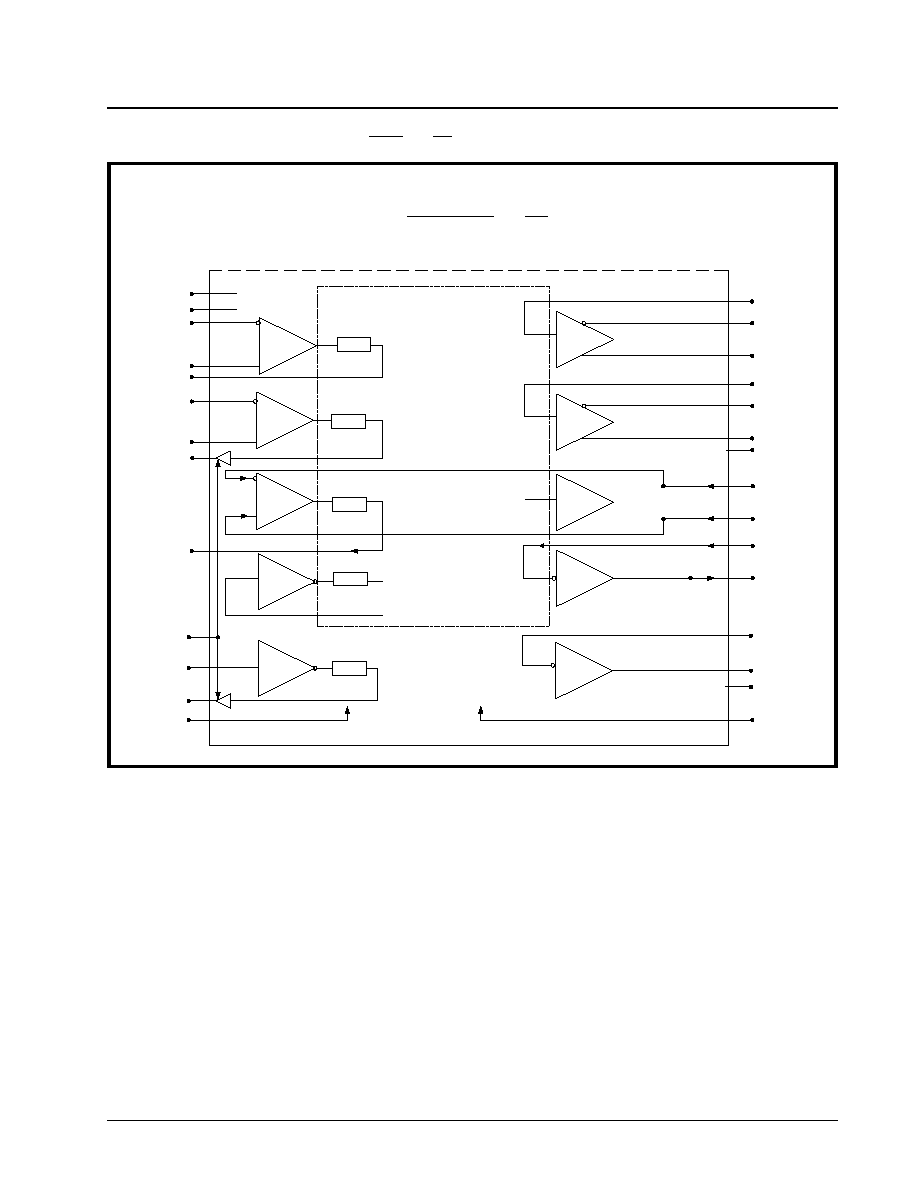
·Á
·Á
·Á
·Á
XRT4500
MULTIPROTOCOL SERIAL NETWORK INTERFACE IC
REV. 1.0.7
69
F
IGURE
42. S
CENARIO
B, MUX2, (DCE/DTE = 0, LP = 1), L
OOP
B
ACK
N
OT
ENABLED
RX8D
RX8I
25
23
RX8
Filter
GND
RX1,2,3
3
RX5B
RX5D
RX5A
36
33
35
RX5
Filter
RX67D
32
RX4,5,6,7
RX7
RX6
Filter
Filter
75
EN_FLTR
8
TX4D
11
TX4A
TX4B
10
TX4
15
TX5D
12
TX5A
TX5B
13
27
TR7
TX7
TX5
9 VDD
TX4,5,6,7,8
29
TR6A
TR6B
30
TX6
28 TX76D
V.11 (RX1,2,3) Termination
80
EN_TERM
Digital MUX 2
Glitch Filter
48
EN_OUT
17
TX8D
19 TX8O
GND
14
TX4,5,6,7,8
TX8
20
VDD
RX4B
RX4D
RX4A
37
40
38
RX4
Filter
SCENARIO B
MUX2 (DCE/DTE = 0, LP = 1)
Loop Back not enabled

XRT4500
·Á
·Á
·Á
·Á
MULTIPROTOCOL SERIAL NETWORK INTERFACE IC
REV. 1.0.7
70
F
IGURE
43. S
CENARIO
C, MUX2, (DCE/DTE = 1, LP = 0)
SCENARIO C
MUX2 (DCE/DTE = 1, LP = 0)
R X 8 D
RX8I
2 5
2 3
R X 8
Filter
G N D
RX1,2,3
3
R X 5 B
R X 5 D
R X 5 A
3 6
3 3
3 5
R X 5
Filter
R X 6 7 D
3 2
RX4,5,6,7
R X 7
R X 6
Filter
Filter
7 5
E N _ F L T R
8
T X 4 D
1 1
T X 4 A
T X 4 B
1 0
T X 4
1 5
T X 5 D
1 2
T X 5 A
T X 5 B
1 3
2 7
T R 7
T X 7
T X 5
9
V D D
TX4,5,6,7,8
2 9
T R 6 A
T R 6 B
3 0
T X 6
2 8 TX76D
V.11 (RX1,2,3) Termination
8 0
E N _ T E R M
Digital MUX 2
Glitch Filter
4 8
E N _ O U T
1 7
T X 8 D
1 9 TX8O
G N D
1 4
TX4,5,6,7,8
T X 8
2 0
V D D
R X 4 B
R X 4 D
R X 4 A
3 7
4 0
3 8
R X 4
Filter

·Á
·Á
·Á
·Á
XRT4500
MULTIPROTOCOL SERIAL NETWORK INTERFACE IC
REV. 1.0.7
71
F
IGURE
44. S
CENARIO
D, MUX2, (DCE/DTE = 1, LP = 1), L
OOP
B
ACK
N
OT
ENABLED
SCENARIO D
MUX 2 (DCE/DTE = 1, LP = 1)
Loop Back not enabled
R X 8 D
RX8I
2 5
2 3
R X 8
Filter
G N D
RX1,2,3
3
R X 5 B
R X 5 D
R X 5 A
3 6
3 3
3 5
R X 5
Filter
R X 6 7 D
3 2
RX4,5,6,7
R X 7
R X 6
Filter
Filter
7 5
E N _ F L T R
8
T X 4 D
1 1
T X 4 A
T X 4 B
1 0
T X 4
1 5
T X 5 D
1 2
T X 5 A
T X 5 B
1 3
2 7
T R 7
T X 7
T X 5
9 VDD
TX4,5,6,7,8
2 9
T R 6 A
T R 6 B
3 0
T X 6
2 8 TX76D
V.11 (RX1,2,3) Termination
8 0
E N _ T E R M
Digital MUX 2
Glitch Filter
4 8
E N _ O U T
1 7
T X 8 D
1 9 TX8O
G N D
1 4
TX4,5,6,7,8
T X 8
2 0
V D D
R X 4 B
R X 4 D
R X 4 A
3 7
4 0
3 8
R X 4
Filter

XRT4500
·Á
·Á
·Á
·Á
MULTIPROTOCOL SERIAL NETWORK INTERFACE IC
REV. 1.0.7
72
F
IGURE
45. S
ERIAL
I
NTERFACE
S
IGNALS
AND
C
ONNECTOR
P
IN
-O
UT
Serial Interface Signals and Connector pin-out
XRT4500
Standard
RS-232
EIA-574
RS-530
RS-449
V.35
X.21
XRT4500
XRT4500
Related standards
V.24
TIA-574
RS422, RS423
RS422, RS423
V.10, V.11, V.28
V.11, X.26
Connector
DB-25
DB-9
DB-25
DB-37
34-pin
15-pin
DTE
DCE
Signal Name
Abrev.
Source
Pin #, Circuit
Pin #
Pin #, Circuit
Pin #, Circuit
Pin, CCITT#
Pin #, Circuit
Pin #, Circuit
Pin #, Circuit
Shield
---
1, ---
1, ---
1, ---
A, ---
1, ---
--, ---
--, ---
Transmitted Data
TXD
DTE
2, BA
3
2, BA (A)
14, BA (B)
4, SD (A)
22, SD (B)
P, 103
S, 103
2, Circuit T (A)
9, Circuit T (B)
63, TX1A
62, TX1B
78, RX1A
79, RX1B
Received Data
RXD
DCE
3, BB
2
3, BB (A)
16, BB (B)
6, RD (A)
24, RD (B)
R, 104
T, 104
4, Circuit R (A)
11, Circuit R (B)
78, RX1A
79, RX1B
63, TX1A
62, TX1B
Request to Send
(Control for X.21)
RTS
DTE
4, CA
7
4, CA (A)
19, CA (B)
7, RS (A)
25, RS (B)
C, 105
3, Circuit C (A)
10, Circuit C (B)
11, TX4A
10, TX4B
37, RX4A
38, RX4B
Clear to Send
(Indication for X.21)
CTS
DCE
5, CB
8
5, CB (A)
13, CB (B)
9, CS (A)
27, CS (B)
D, 106
5, Circuit I (A)
12, Circuit I (B)
37, RX4A
38, RX4B
11, TX4A
10, TX4B
DCE Ready
DSR
DCE
6, CC
6
6, CC (A)
22, CC (B)
11, DM (A)
29, DM (B)
E, 107
36, RX5A
35, RX5B
12, TX5A
13, TX5B
DTE Ready
DTR
DTE
20, CD
4
20, CD (A)
23, CD (B)
12, TR (A)
30, TR (B)
H, 108 *
12, TX5A
13, TX5B
36, RX5A
35, RX5B
Signal Ground ***
---
7, AB
5
7, AB
19, SG
B, 102
8, Circuit G
3, 14, 59, 72
3, 14, 59, 72
Received Line
Signal Detector
DCD
DCE
8, CF
1
8, CF (A)
10, CF (B)
13, RR (A)
31, RR (B)
F, 109
29, TR6A
30, TR6B
29, TR6A
30, TR6B
Transmitter Signal
Element Timing
TXC
DCE
15, DB
15, DB (A)
12, DB (B)
5, ST (A)
23, ST (B)
Y, 114
AA, 114
7, Circuit B (A) **
14, Circuit B (B) **
70, TR3A
71, TR3B
70, TR3A
71, TR3B
Received Signal
Element Timing
RXC
DCE
17, DD
17, DD (A)
9, DD (B)
8, RT (A)
26, RT (B)
V, 115
X, 115
6, Circuit S (A)
13, Circuit S (B)
77, RX2A
76, RX2B
64, TX2A
65, TX2B
Local Loop-back
LL
DTE
18, LL
18, LL
10, LL
L, 141 *
27, TR7
27, TR7
Remote Loop-back
RL
DTE
21, RL
21, RL
14, RL
N, 140 *
19, TX8O
25, RX8I
Ring Indicator
CI
DCE
22, CE
9
--, ----
--, ---
J , 125 *
--, ---
Transmit Signal
Element Timing
SCTE
DTE
24, DA
24, DA (A)
11, DA (B)
17, TT (A)
35, TT (B)
U, 113 *
W, 113 *
7, Circuit X (A) **
14, Circuit X (B) **
64, TX2A
65, TX2B
77, RX2A
76, RX2B
Test Mode
TM
DCE
25, TM
25, TM
18, TM
NN, 142 *
25, RX8I
19, TX8O
Load Resistance
RL=100
RL=120
RL=100
RL=120
Signal Amplitude
±
5 to
±
15 V
0.55 Vpp
Speed per standard
20 to 150kbps
RS422: 10MBp
RS423: 100Kbps
Std: 48kpbs
Max: 10Mbps
V.11: 10Mbps
XRT4500 Speed
256 kbps
V.10: 120 kbps
V.11: 20 Mbps
Mode selection
*
Optional Signal
**
Only o
ne of the two X.21 signals (circuit B or X) can be implemented and be active at one
time
*
*
*
Connect the signal ground to the PCB ground plane of the XRT4500.
(Pins 3, 14, 59 and 72 are the analog grounds for the receivers and transmitters on the XRT4500)

·Á
·Á
·Á
·Á
XRT4500
MULTIPROTOCOL SERIAL NETWORK INTERFACE IC
REV. 1.0.7
73
F
IGURE
46. S
ERIAL
I
NTERFACE
C
ONNECTOR
D
RAWINGS
30
25
20
37
33
19
15
10
5
1
N N
L
R
V
Z
D D
JJ
F
B
M M
LL
B B
D
J
N
T
X
F F
K
P
U
Y
C C
H H
A
E
K K
E E
C
H
M
S
W
A A
13
7
1
25
20
14
1
8
15
9
Serial Interface Connector Drawings
X.21 Connector (ISO 4903)
DTE Connector - DB-15 Pin Male
DCE Connector - DB-15 Pin Female
RS-449 Connector (ISO 4902)
DTE Connector Face - DB-37 Pin Male
DCE Connector Face - DB-37 Pin Female
V.35/ISO 2593 Connector
DTE Connector Face - 34 Pin Male
DCE Connector Face - 34 Pin Female
RS-232 & EIA-530- Connector (ISO 2110)
DTE Connector - DB-25 Pin Male
DCE Connector - DB-25 Pin Female
F
IGURE
46
A
F
IGURE
46
B
F
IGURE
46
D
F
IGURE
46
C

XRT4500
·Á
·Á
·Á
·Á
MULTIPROTOCOL SERIAL NETWORK INTERFACE IC
REV. 1.0.7
74
F
IGURE
47. EIA-530 C
ONNECTION
D
IAGRAM
FOR
XRT4500
EIA-530 Connection Diagram for XRT4500
RX1B
RX1A
TR3A
TX1A
TX1B
RX4A
TX2A
TX4A
TR7
TX5A
RX4B
RX5A
TR6A
RX8I
TX2B
TX5B
TR6B
RX5B
RX2B
RX2A
TR3B
TX8O
TX4B
13
25
12
24
11
23
10
22
9
21
8
20
7
19
6
18
5
17
4
16
3
15
2
14
1
LL A
TXD B
TXD A
TXC A
RXD A
RXD B
RTS A
RXC A
CTS A
DSR A
RTS B
DTR A
DCD A
DSR B
DCD B
DTR B
TXC B
CTS B
RL A
RXC B
SCTE B
SCTE A
RI
3, 14, 59, 77
XRT4500
62
63
70
78
79
11
77
37
27
36
10
12
29
19
76
35
30
13
65
64
71
25
38
TX1B
TX1A
TR3A
RX1A
RX1B
TX4A
RX2A
RX4A
TR7
RX5A
TX4B
TX5A
TR6A
TX8O
RX2B
RX5B
TR6B
TX5B
TX2B
TX2A
TR3B
RX8I
RX4B
13
25
12
24
11
23
10
22
9
21
8
20
7
19
6
18
5
17
4
16
3
15
2
14
1
SCTE B
TXD A
TXD B
SCTE A
RXD B
RXD A
RXC B
RXC A
TXC B
TXC A
CTS B
CTS A
DSR B
DSR A
DCD B
DCD A
RI
RTS A
RTS B
DTR B
DTR A
LL A
RL A
79
78
70
63
62
37
64
11
27
12
38
36
29
25
65
13
30
35
76
77
71
19
10
3, 14, 59, 77
XRT4500
DB25
DCE MODE
P8
DB25
DTE MODE
P4
DTE Mode
DCE Mode
Shield
Shield

·Á
·Á
·Á
·Á
XRT4500
MULTIPROTOCOL SERIAL NETWORK INTERFACE IC
REV. 1.0.7
75
F
IGURE
48. RS-232 C
ONNECTION
D
IAGRAM
FOR
XRT4500
RS-232 Connection Diagram for XRT4500
RX1A
TR3A
TX1A
RX4A
TX2A
TX4A
TR7
TX5A
RX5A
TR6A
RX8I
TX8O
25
21
8
20
7
6
18
5
17
4
3
15
2
1
LL A
TXD A
TXC A
RXD A
RTS A
RXC A
CTS A
DSR A
DTR A
DCD A
DSR B
RL A
RI
3, 14, 59, 77
XRT4500
63
70
78
11
77
37
27
36
12
29
19
64
25
TX1A
TR3A
RX1A
TX4A
RX2A
RX4A
TR7
RX5A
TX5A
TR6A
TX8O
TX2A
RX8I
25
24
21
8
20
7
6
18
5
17
4
3
15
2
1
SCTE B
TXD A
SCTE A
RXD A
RXC A
TXC A
CTS A
DSR A
DCD A
RI
RTS A
DTR A
LL A
RL A
78
70
63
37
64
11
27
12
36
29
25
19
3, 14, 59, 77
XRT4500
P4
DTE MODE
DB25
DCE MODE
P8
DB25
DCE Mode
DTE Mode
Shield
Shield

XRT4500
·Á
·Á
·Á
·Á
MULTIPROTOCOL SERIAL NETWORK INTERFACE IC
REV. 1.0.7
76
S
CENARIOS
1 & 2 N
ORMAL
: `3-
CLOCK
' DCE/DTE I
NTERFACE
O
PERATION
I
NPUT
P
IN
S
ETTINGS
N
OTE
:
1. When M0=1, M2=1, M2=0 the XRT4500 is in the 1 clock (X.21) mode and the 2CK/3CK input pin is ignored.
2. (See Table 8. MUX Connection Table)
DTE (#1)
DCE (#2)
P
IN
#
N
AME
S
TATE
D
ESCRIPTION
P
IN
#
N
AME
S
TATE
D
ESCRIPTION
31
DCE/DTE
0
DTE
31
DCE/DTE
1
DCE
34
EC
1
No Echo
34
EC
1
No Echo
50
2CK/3CK
0
3 clock
50
2CK/3CK
0
3 clock
18
LP
1
No Loopback
18
LP
1
No Loopback
54
CKINV
1
No Invert
54
CKINV
1
No Invert
55
DTINV
1
No Invert
55
DTINV
1
No Invert
53
OSCEN
1
No Internal OSC
53
OSCEN
1
No Internal OSC
HDLC (R)
HDLC (L)
XRT4500
XRT4500
RX1
TX1
RX2
TX2
RX3
TX3
RX2
TX2
RX1
TX1
TXD
SCTE
TXC
RXC
RXD
TXD
SCTE
TXC
RXC
RXD
60
67
73
74
1
78
79
77
76
70
71
64
65
63
62
1
74
68
67
60
63
62
64
65
70
71
77
76
78
79
TXD
SCTE
TXC
RXC
RXD
DTE (#1)
DCE (#2)
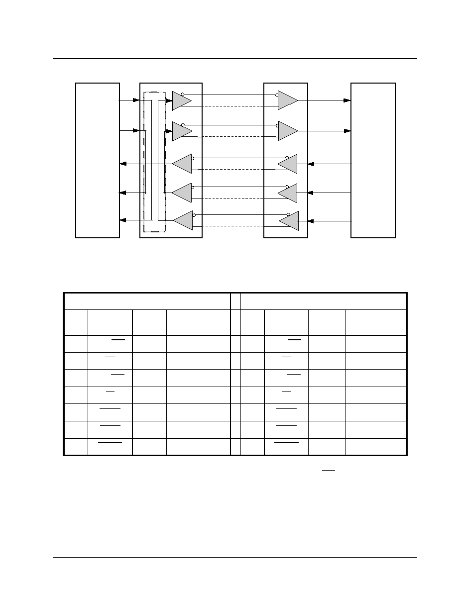
·Á
·Á
·Á
·Á
XRT4500
MULTIPROTOCOL SERIAL NETWORK INTERFACE IC
REV. 1.0.7
77
S
CENARIO
3 &2 DTE L
OOP
-B
ACK
M
ODE
I
NPUT
P
IN
S
ETTINGS
N
OTE
: When M0=1, M2=1, M2=0 the XRT4500 is in the 1 clock (X.21) mode and the 2CK/3CK input pin is ignored.
DTE (#3)
DCE (#2)
P
IN
#
N
AME
S
TATE
D
ESCRIPTION
P
IN
#
N
AME
S
TATE
D
ESCRIPTION
31
DCE/DTE
0
DTE
31
DCE/DTE
1
DCE
34
EC
1
No Echo
34
EC
1
No Echo
50
2CK/3CK
0
3 clock
50
2CK/3CK
0
3 clock
18
LP
0
Loopback
18
LP
1
No Loopback
54
CKINV
1
No Invert
54
CKINV
1
No Invert
55
DTINV
1
No Invert
55
DTINV
1
No Invert
53
OSCEN
1
No Internal OSC
53
OSCEN
1
No Internal OSC
HDLC (R)
HDLC (L)
XRT4500
XRT4500
RX1
TX1
RX2
TX2
RX3
TX3
RX2
TX2
RX1
TX1
TXD
SCTE
TXC
RXC
RXD
TXD
SCTE
TXC
RXC
RXD
60
67
73
74
1
78
79
77
76
70
71
64
65
63
62
1
74
68
67
60
63
62
64
65
70
71
77
76
78
79
TXD
SCTE
TXC
RXC
RXD
DTE (#3)
DCE (#2)
MUX 1
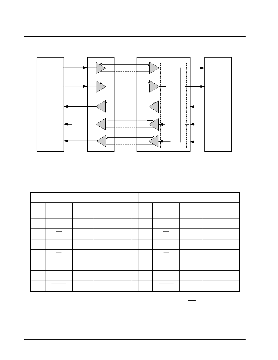
XRT4500
·Á
·Á
·Á
·Á
MULTIPROTOCOL SERIAL NETWORK INTERFACE IC
REV. 1.0.7
78
S
CENARIO
4
C
OMMENTS
: DCE L
OOP
-B
ACK
M
ODE
I
NPUT
P
IN
S
ETTINGS
N
OTE
: When M0=1, M2=1, M2=0 the XRT4500 is in the 1 clock (X.21) mode and the 2CK/3CK input pin is ignored.
DTE (#1)
DCE (#4)
P
IN
#
N
AME
S
TATE
D
ESCRIPTION
P
IN
#
N
AME
S
TATE
D
ESCRIPTION
31
DCE/DTE
0
DTE
31
DCE/DTE
1
DCE
34
EC
1
No Echo
34
EC
1
No Echo
50
2CK/3CK
0
3 Clock
50
2CK/3CK
0
3 clock
18
LP
1
No Loopback
18
LP
0
Loopback
54
CKINV
1
No Invert
54
CKINV
1
No Invert
55
DTINV
1
No Invert
55
DTINV
1
No Invert
53
OSCEN
1
No Internal OSC
53
OSCEN
1
No Internal OSC
HDLC (R)
HDLC (L)
XRT4500
XRT4500
RX1
TX1
RX2
TX2
RX3
TX3
RX2
TX2
RX1
TX1
TXD
SCTE
TXC
RXC
RXD
TXD
SCTE
TXC
RXC
RXD
60
67
73
74
1
78
79
72
76
70
71
64
65
63
62
1
74
68
67
60
63
62
64
65
70
71
77
76
78
79
TXD
SCTE
TXC
RXC
RXD
DCE (#4)
DTE (#1)
MUX 1

·Á
·Á
·Á
·Á
XRT4500
MULTIPROTOCOL SERIAL NETWORK INTERFACE IC
REV. 1.0.7
79
S
CENARIO
5 & 2
C
OMMENTS
: TXC C
LOCK
I
NVERSION
IN
DTE M
ODE
I
NPUT
P
IN
S
ETTINGS
N
OTE
: When M0=1, M2=1, M2=0 the XRT4500 is in the 1 clock (X.21) mode and the 2CK/3CK input pin is ignored.
DTE (#5)
DCE (#2)
P
IN
#
N
AME
S
TATE
D
ESCRIPTION
P
IN
#
N
AME
S
TATE
D
ESCRIPTION
31
DCE/DTE
0
DTE
31
DCE/DTE
1
DCE
34
EC
1
No Echo
34
EC
1
No Echo
50
2CK/3CK
0
3 clock
50
2CK/3CK
0
3 clock
18
LP
1
No Loopback
18
LP
1
No Loopback
54
CKINV
0
Invert
54
CKINV
1
No Invert
55
DTINV
1
No Invert
55
DTINV
1
No Invert
53
OSCEN
1
No Internal OSC
53
OSCEN
1
No Internal OSC
HDLC (R)
HDLC (L)
XRT4500
XRT4500
RX1
TX1
RX2
TX2
RX3
TX3
RX2
TX2
RX1
TX1
TXD
SCTE
TXC
RXC
RXD
TXD
SCTE
TXC
RXC
RXD
60
67
73
74
1
78
79
72
76
70
71
64
65
63
62
1
74
68
67
60
63
62
64
65
70
71
77
76
78
79
TXD
SCTE
TXC
RXC
RXD
DCE (#2)
DTE (#5)

XRT4500
·Á
·Á
·Á
·Á
MULTIPROTOCOL SERIAL NETWORK INTERFACE IC
REV. 1.0.7
80
S
CENARIO
6
C
OMMENTS
: TXC C
LOCK
I
NVERSION
IN
DCE M
ODE
I
NPUT
P
IN
S
ETTINGS
N
OTE
: When M0=1, M2=1, M2=0 the XRT4500 is in the 1 clock (X.21) mode and the 2CK/3CK input pin is ignored.
DTE (#1)
DCE (#6)
P
IN
#
N
AME
S
TATE
D
ESCRIPTION
P
IN
#
N
AME
S
TATE
D
ESCRIPTION
31
DCE/DTE
0
DTE
31
DCE/DTE
1
DCE
34
EC
1
No Echo
34
EC
1
No Echo
50
2CK/3CK
0
3 clock
50
2CK/3CK
0
3 clock
18
LP
1
No Loopback
18
LP
1
No Loopback
54
CKINV
1
No Invert
54
CKINV
0
Invert
55
DTINV
1
No Invert
55
DTINV
1
No Invert
53
OSCEN
1
No Internal OSC
53
OSCEN
1
No Internal OSC
DTE (#1)
HDLC (L)
XRT4500
XRT4500
RX1
TX1
RX2
TX2
RX3
TX3
RX2
TX2
RX1
TX1
TXD
SCTE
TXC
RXC
RXD
TXD
SCTE
TXC
RXC
RXD
60
67
73
74
1
78
79
72
76
70
71
64
65
63
62
1
74
68
67
60
63
62
64
65
70
71
77
76
78
79
TXD
SCTE
TXC
RXC
RXD
DCE (#6)
HDLC (R)

·Á
·Á
·Á
·Á
XRT4500
MULTIPROTOCOL SERIAL NETWORK INTERFACE IC
REV. 1.0.7
81
S
CENARIO
7 & 2
I
NPUT
P
IN
S
ETTINGS
N
OTE
: When M0=1, M2=1, M2=0 the XRT4500 is in the 1 clock (X.21) mode and the 2CK/3CK input pin is ignored.
DTE (#7)
DCE (#2)
P
IN
#
N
AME
S
TATE
D
ESCRIPTION
P
IN
#
N
AME
S
TATE
D
ESCRIPTION
31
DCE/DTE
0
DTE
31
DCE/DTE
1
DCE
34
EC
1
No Echo
34
EC
1
No Echo
50
2CK/3CK
0
3 clock
50
2CK/3CK
0
3 clock
18
LP
0
Loopback
18
LP
1
No Loopback
54
CKINV
0
Invert
54
CKINV
1
No Invert
55
DTINV
1
No Invert
55
DTINV
1
No Invert
53
OSCEN
1
No Internal OSC
53
OSCEN
1
No Internal OSC
HDLC (R)
HDLC (L)
XRT4500
XRT4500
RX1
TX1
RX2
TX2
RX3
TX3
RX2
TX2
RX1
TX1
TXD
SCTE
TXC
RXC
RXD
TXD
SCTE
TXC
RXC
RXD
60
67
73
74
1
78
79
72
76
70
71
64
65
63
62
1
74
68
67
60
63
62
64
65
70
71
77
76
78
79
TXD
SCTE
TXC
RXC
RXD
DCE (#2)
DTE (#7)
MUX 1

XRT4500
·Á
·Á
·Á
·Á
MULTIPROTOCOL SERIAL NETWORK INTERFACE IC
REV. 1.0.7
82
S
CENARIO
8
I
NPUT
P
IN
S
ETTINGS
N
OTE
: When M0=1, M2=1, M2=0 the XRT4500 is in the 1 clock (X.21) mode and the 2CK/3CK input pin is ignored.
DTE (#1)
DCE (#8)
P
IN
#
N
AME
S
TATE
D
ESCRIPTION
P
IN
#
N
AME
S
TATE
D
ESCRIPTION
31
DCE/DTE
0
DTE
31
DCE/DTE
1
DCE
34
EC
1
No Echo
34
EC
1
No Echo
50
2CK/3CK
0
3 clock
50
2CK/3CK
0
3 clock
18
LP
1
No Loopback
18
LP
0
Loopback
54
CKINV
1
No Invert
54
CKINV
0
Invert
55
DTINV
1
No Invert
55
DTINV
1
No Invert
53
OSCEN
1
No Internal OSC
53
OSCEN
1
No Internal OSC
HDLC (R)
HDLC (L)
XRT4500
XRT4500
RX1
TX1
RX2
TX2
RX3
TX3
RX2
TX2
RX1
TX1
TXD
SCTE
TXC
RXC
RXD
TXD
SCTE
TXC
RXC
RXD
60
76
73
74
1
78
79
72
76
70
71
64
65
63
62
1
74
68
67
60
63
62
64
65
70
71
77
76
78
79
TXD
SCTE
TXC
RXC
RXD
DCE (#8)
DCE (#1)
MUX 1

·Á
·Á
·Á
·Á
XRT4500
MULTIPROTOCOL SERIAL NETWORK INTERFACE IC
REV. 1.0.7
83
S
CENARIO
9 & 10
C
OMMENTS
: 2 C
LOCK
M
ODE
O
PERATION
W
ITHIN
THE
`DCE M
ODE
'. T
HIS
FEATURE
IS
U
SEFUL
F
OR
A
PPLICATIONS
T
HAT
I
NTERFACE
TO
A
D
EVICE
W
HICH
D
OES
N
OT
S
UPPLY
`SCTE' C
LOCK
S
IGNAL
I
NPUT
P
IN
S
ETTINGS
N
OTE
: When M0=1, M2=1, M2=0 the XRT4500 is in the 1 clock (X.21) mode and the 2CK/3CK input pin is ignored.
DTE (#9)
DCE (#10)
P
IN
#
N
AME
S
TATE
D
ESCRIPTION
P
IN
#
N
AME
S
TATE
D
ESCRIPTION
31
DCE/DTE
0
DTE
31
DCE/DTE
1
DCE
34
EC
1
No Echo
34
EC
1
No Echo
50
2CK/3CK
X
Don't Care
50
2CK/3CK
1
2 clock
18
LP
1
No Loopback
18
LP
1
No Loopback
54
CKINV
1
No Invert
54
CKINV
1
No Invert
55
DTINV
1
No Invert
55
DTINV
1
No Invert
53
OSCEN
1
No Internal OSC
53
OSCEN
1
No Internal OSC
DCE (#10)
HDLC (L)
XRT4500
XRT4500
RX1
TX1
RX2
TX2
RX3
TX3
RX2
TX2
RX1
TX1
TXD
SCTE
TXC
RXC
RXD
TXD
SCTE
TXC
RXC
RXD
60
67
73
74
1
78
79
72
76
70
71
64
65
63
62
1
74
68
67
60
63
62
64
65
70
71
77
76
78
79
TXD
TXC
RXC
RXD
HDLC (R)
DTE (#9)

XRT4500
·Á
·Á
·Á
·Á
MULTIPROTOCOL SERIAL NETWORK INTERFACE IC
REV. 1.0.7
84
S
CENARIO
12
I
NPUT
P
IN
S
ETTINGS
N
OTE
: When M0=1, M2=1, M2=0 the XRT4500 is in the 1 clock (X.21) mode and the 2CK/3CK input pin is ignored.
DTE (#9)
DCE (#12)
P
IN
#
N
AME
S
TATE
D
ESCRIPTION
P
IN
#
N
AME
S
TATE
D
ESCRIPTION
31
DCE/DTE
0
DTE
31
DCE/DTE
1
DCE
34
EC
1
No Echo
34
EC
1
No Echo
50
2CK/3CK
0
3 clock
50
2CK/3CK
1
2 clock
18
LP
1
No Loopback
18
LP
0
Loopback
54
CKINV
1
No Invert
54
CKINV
1
No Invert
55
DTINV
1
No Invert
55
DTINV
1
No Invert
53
OSCEN
1
No Internal OSC
53
OSCEN
1
No Internal OSC
HDLC (R)
HDLC (L)
XRT4500
XRT4500
RX1
TX1
RX2
TX2
RX3
TX3
RX2
TX2
RX1
TX1
TXD
SCTE
TXC
RXC
RXD
TXD
SCTE
TXC
RXC
RXD
60
67
73
74
1
78
79
72
76
70
71
64
65
63
62
1
75
68
67
60
63
62
64
65
70
71
77
76
78
79
TXD
TXC
RXC
RXD
DCE (#12)
DTE (#9)
MUX 1

·Á
·Á
·Á
·Á
XRT4500
MULTIPROTOCOL SERIAL NETWORK INTERFACE IC
REV. 1.0.7
85
S
CENARIO
13 & 10
I
NPUT
P
IN
S
ETTINGS
N
OTE
: When M0=1, M2=1, M2=0 the XRT4500 is in the 1 clock (X.21) mode and the 2CK/3CK input pin is ignored.
DTE (#13)
DCE (#10)
P
IN
#
N
AME
S
TATE
D
ESCRIPTION
P
IN
#
N
AME
S
TATE
D
ESCRIPTION
31
DCE/DTE
0
DTE
31
DCE/DTE
1
DCE
34
EC
1
No Echo
34
EC
1
No Echo
50
2CK/3CK
1
2 clock
50
2CK/3CK
1
2 clock
18
LP
1
No Loopback
18
LP
1
No Loopback
54
CKINV
0
Invert
54
CKINV
1
No Invert
55
DTINV
1
No Invert
55
DTINV
1
No Invert
53
OSCEN
1
No Internal OSC
53
OSCEN
1
No Internal OSC
HDLC (R)
HDLC (L)
XRT4500
XRT4500
RX1
TX1
RX2
TX2
RX3
TX3
RX2
TX2
RX1
TX1
TXD
SCTE
TXC
RXC
RXD
TXD
SCTE
TXC
RXC
RXD
60
67
73
74
1
78
79
72
76
70
71
64
65
63
62
1
74
68
67
60
63
62
64
65
70
71
77
76
78
79
TXD
TXC
RXC
RXD
DTE (#13)
DCE (#10)

XRT4500
·Á
·Á
·Á
·Á
MULTIPROTOCOL SERIAL NETWORK INTERFACE IC
REV. 1.0.7
86
S
CENARIO
14
C
OMMENTS
: TXC C
LOCK
I
NVERSION
AND
2 C
LOCK
M
ODE
O
PERATION
W
ITHIN
T
HE
DCE M
ODE
. T
HIS
S
CENARIO
C
AN
BE
U
SED
TO
R
ESOLVE
THE
2 C
LOCK
P
ROPAGATION
D
ELAY
T
IMING
V
IOLATION
I
SSUE
.
I
NPUT
P
IN
S
ETTINGS
N
OTE
: When M0=1, M2=1, M2=0 the XRT4500 is in the 1 clock (X.21) mode and the 2CK/3CK input pin is ignored.
DTE
DCE
P
IN
#
N
AME
S
TATE
D
ESCRIPTION
P
IN
#
N
AME
S
TATE
D
ESCRIPTION
31
DCE/DTE
0
DTE
31
DCE/DTE
1
DCE
34
EC
1
No Echo
34
EC
1
No Echo
50
2CK/3CK
1
2 clock
50
2CK/3CK
1
2 clock
18
LP
1
No Loopback
18
LP
1
No Loopback
54
CKINV
1
No Invert
54
CKINV
0
Invert
55
DTINV
1
No Invert
55
DTINV
1
No Invert
53
OSCEN
1
No Internal OSC
53
OSCEN
1
No Internal OSC
HDLC (R)
HDLC (L)
XRT4500
XRT4500
RX1
TX1
RX2
TX2
RX3
TX3
RX2
TX2
RX1
TX1
TXD
SCTE
TXC
RXC
RXD
TXD
SCTE
TXC
RXC
RXD
60
67
73
74
1
78
79
72
76
70
71
64
65
63
62
1
74
68
67
60
63
62
64
65
70
71
77
76
78
79
TXD
TXC
RXC
RXD
DTE (#13)
DCE (#14)

·Á
·Á
·Á
·Á
XRT4500
MULTIPROTOCOL SERIAL NETWORK INTERFACE IC
REV. 1.0.7
87
S
CENARIO
16
I
NPUT
P
IN
S
ETTINGS
N
OTE
: When M0=1, M2=1, M2=0 the XRT4500 is in the 1 clock (X.21) mode and the 2CK/3CK input pin is ignored.
DTE (#9)
DCE (#16)
P
IN
#
N
AME
S
TATE
D
ESCRIPTION
P
IN
#
N
AME
S
TATE
D
ESCRIPTION
31
DCE/DTE
0
DTE
31
DCE/DTE
1
DCE
34
EC
1
No Echo
34
EC
1
No Echo
50
2CK/3CK
1
2 clock
50
2CK/3CK
1
2 clock
18
LP
1
No Loopback
18
LP
0
Loopback
54
CKINV
1
No Invert
54
CKINV
0
Invert
55
DTINV
1
No Invert
55
DTINV
1
No Invert
53
OSCEN
1
No Internal OSC
53
OSCEN
1
No Internal OSC
HDLC (R)
HDLC (L)
XRT4500
XRT4500
RX1
TX1
RX2
TX2
RX3
TX3
RX2
TX2
RX1
TX1
TXD
SCTE
TXC
RXC
RXD
TXD
SCTE
TXC
RXC
RXD
60
67
73
74
1
78
79
72
76
70
71
64
65
63
62
1
74
68
67
60
63
62
64
65
70
71
77
76
78
79
TXD
TXC
RXC
RXD
DTE (#9)
DCE (#16)
MUX 1

XRT4500
·Á
·Á
·Á
·Á
MULTIPROTOCOL SERIAL NETWORK INTERFACE IC
REV. 1.0.7
88
S
CENARIO
17 & 18
C
OMMENTS
: X:21 M
ODE
O
PERATION
I
NPUT
P
IN
S
ETTINGS
(1
CLOCK
MODE
)
N
OTE
: When M0=1, M2=1, M2=0 the XRT4500 is in the 1 clock (X.21) mode and the 2CK/3CK input pin is ignored.
DTE (#17)
DCE (#18)
P
IN
#
N
AME
S
TATE
D
ESCRIPTION
P
IN
#
N
AME
S
TATE
D
ESCRIPTION
31
DCE/DTE
0
DTE
31
DCE/DTE
1
DCE
34
EC
1
No Echo
34
EC
1
No Echo
50
2CK/3CK
X
Don't care
50
2CK/3CK
X
Don't care
18
LP
1
No Loopback
18
LP
1
No Loopback
54
CKINV
1
No Invert
54
CKINV
1
No Invert
55
DTINV
1
No Invert
55
DTINV
1
No Invert
53
OSCEN
1
No Internal OSC
53
OSCEN
1
No Internal OSC
HDLC (R)
HDLC (L)
XRT4500
XRT4500
RX1
TX1
RX2
TX2
RX3
TX3
RX2
TX2
RX1
TX1
TXD
SCTE
TXC
RXC
RXD
TXD
SCTE
TXC
RXC
RXD
60
67
73
74
1
78
79
72
76
70
71
64
65
64
62
1
74
68
67
60
63
62
64
65
70
71
77
76
78
79
TXD
RXC
RXD
DTE (#17)
DCE (#18)

·Á
·Á
·Á
·Á
XRT4500
MULTIPROTOCOL SERIAL NETWORK INTERFACE IC
REV. 1.0.7
89
S
CENARIO
20
I
NPUT
P
IN
S
ETTINGS
(1
CLOCK
MODE
)
N
OTE
: When M0=1, M2=1, M2=0 the XRT4500 is in the 1 clock (X.21) mode and the 2CK/3CK input pin is ignored.
DTE (#17)
DCE (#20)
P
IN
#
N
AME
S
TATE
D
ESCRIPTION
P
IN
#
N
AME
S
TATE
D
ESCRIPTION
31
DCE/DTE
0
DTE
31
DCE/DTE
1
DCE
34
EC
1
No Echo
34
EC
1
No Echo
50
2CK/3CK
X
Don't care
50
2CK/3CK
X
Don't care
18
LP
1
No Loopback
18
LP
0
Loopback
54
CKINV
1
No Invert
54
CKINV
1
No Invert
55
DTINV
1
No Invert
55
DTINV
1
No Invert
53
OSCEN
1
No Internal OSC
53
OSCEN
1
No Internal OSC
HDLC (R)
HDLC (L)
XRT4500
XRT4500
RX1
TX1
RX2
TX2
RX3
TX3
RX2
TX2
RX1
TX1
TXD
SCTE
TXC
RXC
RXD
TXD
SCTE
TXC
RXC
RXD
60
67
73
74
1
78
79
72
76
70
71
64
65
63
62
1
74
68
67
60
63
62
64
65
70
71
77
76
78
79
TXD
RXC
RXD
DTE (#17)
DCE (#20)
MUX 1

XRT4500
·Á
·Á
·Á
·Á
MULTIPROTOCOL SERIAL NETWORK INTERFACE IC
REV. 1.0.7
90
S
CENARIO
21
I
NPUT
P
IN
S
ETTINGS
(1
CLOCK
MODE
)
N
OTE
: When M0=1, M2=1, M2=0 the XRT4500 is in the 1 clock (X.21) mode and the 2CK/3CK input pin is ignored.
DTE (#21)
DCE (#18)
P
IN
#
N
AME
S
TATE
D
ESCRIPTION
P
IN
#
N
AME
S
TATE
D
ESCRIPTION
31
DCE/DTE
0
DTE
31
DCE/DTE
1
DCE
34
EC
1
No Echo
34
EC
1
No Echo
50
2CK/3CK
X
Don't care
50
2CK/3CK
X
Don't care
18
LP
1
No Loopback
18
LP
1
No Loopback
54
CKINV
0
Invert
54
CKINV
1
No Invert
55
DTINV
1
No Invert
55
DTINV
1
No Invert
53
OSCEN
1
No Internal OSC
53
OSCEN
1
No Internal OSC
HDLC (R)
HDLC (L)
XRT4500
XRT4500
TX1
RX2
TX2
RX3
TX3
RX2
TX2
RX1
TX1
TXD
SCTE
TXC
RXC
RXD
TXD
SCTE
TXC
RXC
RXD
60
67
73
74
1
78
79
72
76
70
71
64
65
63
62
1
74
68
67
60
63
62
64
65
70
61
77
76
78
79
TXD
RXC
RXD
DTE (#21)
DCE (#18)
RX1

·Á
·Á
·Á
·Á
XRT4500
MULTIPROTOCOL SERIAL NETWORK INTERFACE IC
REV. 1.0.7
91
S
CENARIO
22
I
NPUT
P
IN
S
ETTINGS
(1
CLOCK
MODE
)
N
OTE
: When M0=1, M2=1, M2=0 the XRT4500 is in the 1 clock (X.21) mode and the 2CK/3CK input pin is ignored.
DTE (#17)
DCE (#22)
P
IN
#
N
AME
S
TATE
D
ESCRIPTION
P
IN
#
N
AME
S
TATE
D
ESCRIPTION
31
DCE/DTE
0
DTE
31
DCE/DTE
1
DCE
34
EC
1
No Echo
34
EC
1
No Echo
50
2CK/3CK
X
Don't care
50
2CK/3CK
X
Don't care
18
LP
1
No Loopback
18
LP
1
No Loopback
54
CKINV
1
No Invert
54
CKINV
0
Invert
55
DTINV
1
No Invert
55
DTINV
1
No Invert
53
OSCEN
1
No Internal OSC
53
OSCEN
1
No Internal OSC
HDLC (R)
HDLC (L)
XRT4500
XRT4500
RX1
TX1
RX2
TX2
RX3
TX3
RX2
TX2
RX1
TX1
TXD
SCTE
TXC
RXC
RXD
TXD
SCTE
TXC
RXC
RXD
60
67
73
74
1
78
79
72
76
70
71
64
65
63
62
1
74
68
67
60
63
62
64
65
70
71
77
76
78
79
TXD
RXC
RXD
DTE (#17)
DCE (#22)

XRT4500
·Á
·Á
·Á
·Á
MULTIPROTOCOL SERIAL NETWORK INTERFACE IC
REV. 1.0.7
92
S
CENARIO
23
I
NPUT
P
IN
S
ETTINGS
(1
CLOCK
MODE
)
N
OTE
: When M0=1, M2=1, M2=0 the XRT4500 is in the 1 clock (X.21) mode and the 2CK/3CK input pin is ignored.
DTE (#23)
DCE (#18)
P
IN
#
N
AME
S
TATE
D
ESCRIPTION
P
IN
#
N
AME
S
TATE
D
ESCRIPTION
31
DCE/DTE
0
DTE
31
DCE/DTE
1
DCE
34
EC
1
No Echo
34
EC
1
No Echo
50
2CK/3CK
X
Don't care
50
2CK/3CK
X
Don't care
18
LP
0
Loopback
18
LP
1
No Loopback
54
CKINV
0
Invert
54
CKINV
1
No Invert
55
DTINV
1
No Invert
55
DTINV
1
No Invert
53
OSCEN
1
No Internal OSC
53
OSCEN
1
No Internal OSC
H D L C ( R )
H D L C ( L )
XRT4500
XRT4500
R X 1
T X 1
R X 2
T X 2
T X 3
R X 2
T X 2
R X 1
T X 1
T X D
S C T E
T X C
R X C
R X D
T X D
S C T E
T X C
R X C
R X D
6 0
6 7
7 3
7 4
1
7 8
7 9
7 2
7 6
7 0
7 1
6 4
6 5
6 3
6 2
1
7 4
6 8
6 7
6 0
6 3
6 2
6 4
6 5
7 0
6 1
7 7
7 6
7 8
7 9
T X D
R X C
R X D
DTE #23)
DCE (#18)
MUX 1
R X 3

·Á
·Á
·Á
·Á
XRT4500
MULTIPROTOCOL SERIAL NETWORK INTERFACE IC
REV. 1.0.7
93
S
CENARIO
48
I
NPUT
P
IN
S
ETTINGS
(1
CLOCK
MODE
)
N
OTE
: When M0=1, M2=1, M2=0 the XRT4500 is in the 1 clock (X.21) mode and the 2CK/3CK input pin is ignored.
DTE (#17)
DCE (#48)
P
IN
#
N
AME
S
TATE
D
ESCRIPTION
P
IN
#
N
AME
S
TATE
D
ESCRIPTION
31
DCE/DTE
0
DTE
31
DCE/DTE
1
DCE
34
EC
1
No Echo
34
EC
0
Echo Mode
50
2CK/3CK
X
Don't care
50
2CK/3CK
X
Don't care
18
LP
1
No Loopback
18
LP
0
Loopback
54
CKINV
1
No Invert
54
CKINV
0
Invert
55
DTINV
1
No Invert
55
DTINV
1
No Invert
53
OSCEN
1
No Internal OSC
53
OSCEN
1
No Internal OSC
HDLC (R)
HDLC (L)
XRT4500
XRT4500
RX1
TX1
RX2
TX2
RX3
TX3
RX2
TX2
RX1
TX1
TXD
SCTE
TXC
RXC
RXD
TXD
SCTE
TXC
RXC
RXD
60
67
73
74
1
78
79
72
76
70
71
64
65
63
62
1
74
68
67
60
63
62
64
65
70
61
77
76
78
79
TXD
RXC
RXD
DTE (#17)
DCE #48)
CLK
Q
D

XRT4500
·Á
·Á
·Á
·Á
MULTIPROTOCOL SERIAL NETWORK INTERFACE IC
REV. 1.0.7
94
External Components used by the XRT4500
Function
Description
Notes
V
SS
by-pass Capacitor
25-47
µ
F, 12V, SMT Tantalum
-6V switching Regulator filter.
Low ESR. (0.20
max at 100kHz)
Sprague Type
SPR595D476X9025R2T-X
Schottky Diode
1N5819 40V, 1A.
Must be Schottky type
Inductor
47 or 68
µ
H SMT inductor
JW Miller PM105-470K or PM105-
680k.
Coilcraft D03316P-473
Current Sense Resistor
0.5
, 0.5W, 5%
Charge Pump Capacitor
2.2
µ
F, 25V, SMT Tantalum
+12V Charge Pump
V
PP
by-pass Capacitor
10
µ
F, 25V, SMT Tantalum
+12V Charge Pump
V
DD
by-pass Capacitor
22
µ
F, 16V, Electrolytic
+5V decoupling. (In addition to
various 0.1
µ
F, 50V capacitors)
General by-pass
Capacitors
0.1
µ
F, 50V
Panasonic X7R Dielectric, 1206
size.
Digikey PCC104BCT-ND
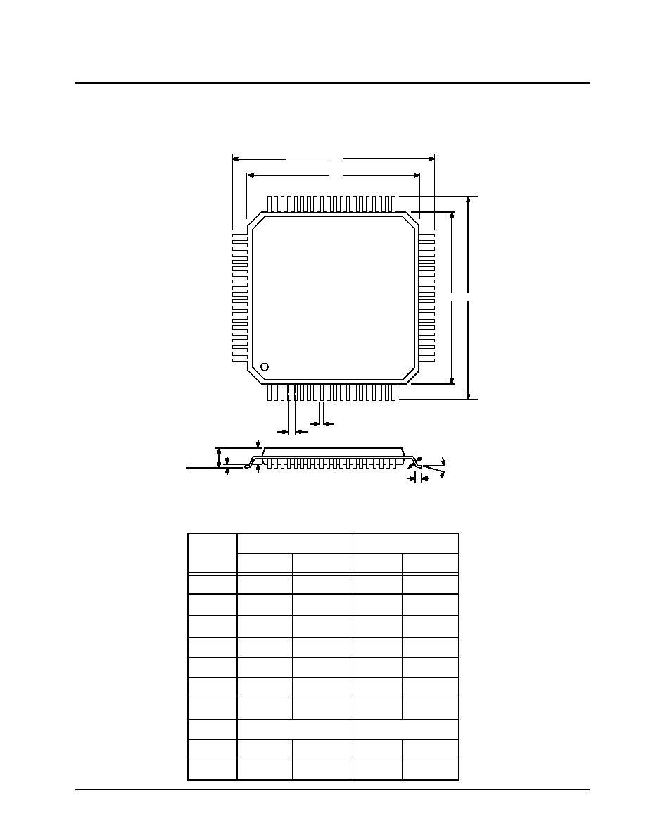
·Á
·Á
·Á
·Á
XRT4500
MULTIPROTOCOL SERIAL NETWORK INTERFACE IC
REV. 1.0.7
95
Note: The control dimension is the millimeter column
INCHES
MILLIMETERS
SYMBOL
MIN
MAX
MIN
MAX
A
0.055
0.063
1.40
1.60
A
1
0.002
0.006
0.05
0.15
A
2
0.053
0.057
1.35
1.45
B
0.009
0.015
0.22
0.38
C
0.004
0.008
0.09
0.20
D
0.622
0.638
15.80
16.20
D
1
0.547
0.555
13.90
14.10
e
0.0256 BSC
0.65 BSC
L
0.018
0.030
0.45
0.75
0
∞
7
∞
0
∞
7
∞
60
41
40
21
1
2
0
61
80
D
D1
D
D1
B
e
A2
A1
A
Seating Plane
L
C
80 LEAD THIN QUAD FLAT PACK
(14 x 14 x 1.4 mm TQFP)
REV. 3.00

·Á
·Á
·Á
·Á
XRT4500
MULTIPROTOCOL SERIAL NETWORK INTERFACE IC
REV. 1.0.7
96
NOTICE
EXAR Corporation reserves the right to make changes to the products contained in this publication in order
to improve design, performance or reliability. EXAR Corporation assumes no responsibility for the use of
any circuits described herein, conveys no license under any patent or other right, and makes no represen-
tation that the circuits are free of patent infringement. Charts and schedules contained here in are only for
illustration purposes and may vary depending upon a user's specific application. While the information in
this publication has been carefully checked; no responsibility, however, is assumed for inaccuracies.
EXAR Corporation does not recommend the use of any of its products in life support applications where
the failure or malfunction of the product can reasonably be expected to cause failure of the life support sys-
tem or to significantly affect its safety or effectiveness. Products are not authorized for use in such applica-
tions unless EXAR Corporation receives, in writing, assurances to its satisfaction that: (a) the risk of injury
or damage has been minimized; (b) the user assumes all such risks; (c) potential liability of EXAR Corpo-
ration is adequately protected under the circumstances.
Copyright 2002 EXAR Corporation
Datasheet September 2002.
Reproduction, in part or whole, without the prior written consent of EXAR Corporation is prohibited.
REVISIONS
Rev. 1.0.3 -- Updated electrical characteristics, made minor text edits.
Rev. 1.0.4 -- Corrected page formatting problems.
Rev. 1.0.5 -- Corrected table anchor format problem page 46 (caused text to hide), replaced TR3 with TR6
page 41.
Rev. 1.0.6 -- Figure 2: Supply current vs. Temp, edited IDD values.
Rev. 1.0.7 -- Table 1, Receiver specs V.35-- Min Signal level =
±
250mV, Max Signal Peak =
±10V, DC Rin =
175
. Table 6, Switch S4 V.28 changed from Open to Closed.