XR-T5683A
...the analog plus company
TM
PCM Line
Interface Chip
Rev. 2.01
E
1995
EXAR Corporation, 48720 Kato Road, Fremont, CA 94538
z
(510) 668-7000
z
FAX (510) 668-7017
1
June 1997-3
FEATURES
D
Single 5V Supply
D
Receiver Input Can Be Either Balanced or
Unbalanced
D
Up To 8.448Mbps Operation In Both Tx and Rx
Directions
D
TTL Compatible Interface
D
Device Can Be Used as a Line Interface Unit With-
out Clock Recovery
APPLICATIONS
D
T1, T2, E1 & E2 Rates, PCM Line Interface
D
Network Multiplexing and Terminating Equipment
GENERAL DESCRIPTION
The XR-T5683A is a PCM line interface chip consisting of
both transmit and receive circuitry. This device is offered
in a plastic dual in-line (PDIP) or in a surface mount
package (SOIC). The maximum bit rate of the chip is
8.448Mbps, and the signal level to the receiver can be
attenuated by -10dB cable loss at one-half the bit rate. At
nominal supply voltage operation, the typical current
consumption is 40mA.
ORDERING INFORMATION
Part No.
Package
Operating
Temperature Range
XR-T5683AIP
18 Lead 300 Mil PDIP
-40
∞
C to +85
∞
C
XR-T5683AID
18 Lead 300 Mil JEDEC SOIC
-40
∞
C to +85
∞
C
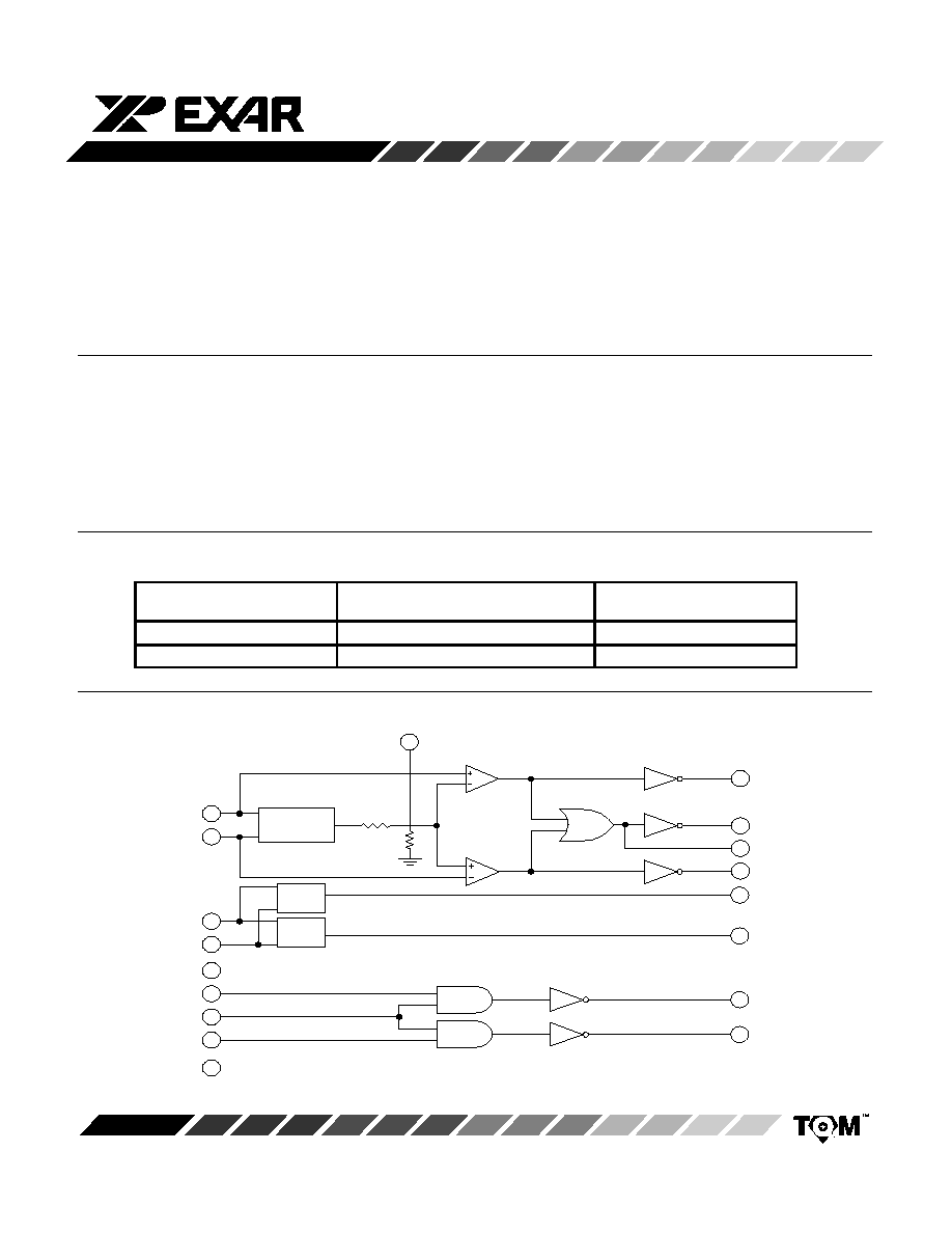
BLOCK DIAGRAM
Figure 1. Block Diagram
RPOS
11
Positive
Threshold
Comparator
PDC
1
Peak
Detector
BIAS
RXDATA+ 2
RXDATA- 3
Negative
Threshold
Comparator
TE
4
TTL Buffer
TANK BIAS
6
RNEG
10
RCLK
8
BIAS
5
TXDATA+
13
Open Collector
Driver
BIAS
TV
CC
18
RGND 7
RV
CC
9
TPOS 17
TCLK 16
TNEG 12
TGND 14
TXDATA-
15
Open Collector
Driver
TTL Buffer
TTL Buffer
XR-T5683A
2
Rev. 2.01
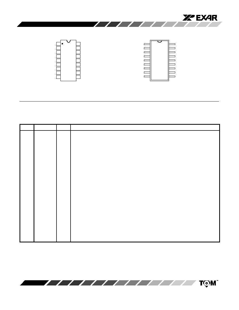
PIN CONFIGURATION
18 Lead PDIP (0.300")
1
2
3
4
5
6
7
8
9
18
17
16
15
14
13
12
11
10
TV
CC
TPOS
TCLK
TXDATA-
PDC
RXDATA+
RXDATA-
TE
TGND
TXDATA+
TNEG
RPOS
BIAS
TANK BIAS
RGND
RCLK
RNEG
RV
CC
18 Lead SOIC (JEDEC, 0.300")
18
1
10
9
2
3
4
5
6
7
15
14
13
12
11
17
16
8
PDC
RXDATA+
RXDATA-
TE
BIAS
TANK BIAS
RGND
RCLK
RV
CC
TV
CC
TPOS
TCLK
TXDATA-
TGND
TXDATA+
TNEG
RPOS
RNEG
PIN DESCRIPTION
Pin #
Symbol
Type
Description
1
PDC
Peak Detector Capacitor. This pin should be connected to a 0.1
µ
F capacitor.
2
RXDATA+
I
Receive Analog Input Positive. Line analog input.
3
RXDATA-
I
Receive Analog Input Negative. Line analog input.
4
TE
O
Tank Excitation Output. This output connects to one side of the tank circuitry.
5
BIAS
O
Bias. This output is to be connected to the center tap of the receive transformer.
6
TANK BIAS
O
Tank Bias. The tank circuitry is biased via this output.
7
RGND
Receiver Ground. To minimize ground interference a separate pin is used to ground the
receive section.
8
RCLK
O
Recovered Receive Clock. Recovered clock signal to the terminal equipment.
9
RV
CC
Receive Supply Voltage. 5V supply voltage to the receive section.
10
RNEG
O
Receive Negative Data. Negative pulse data output to the terminal equipment (active low).
11
RPOS
O
Receive Positive Data. Positive pulse data output to the terminal equipment (active low).
12
TNEG
I
Transmit Negative Data. TNEG is valid while TCLK is high.
13
TXDATA+
O
Transmit Positive Output. Transmit bipolar signal is driven to the line via a transformer.
14
TGND
Transmit Ground.
15
TXDATA-
O
Transmit Negative Output. Transmit bipolar signal is driven to the line via a transformer.
16
TCLK
I
Transmit Clock. Timing element for TPOS and TNEG.
17
TPOS
I
Transmit Positive Data. TPOS is valid while TCLK is high.
18
TV
CC
Transmit Supply Voltage. 5V supply voltage to the transmit section.
XR-T5683A
3
Rev. 2.01
ELECTRICAL CHARACTERISTICS
Test Conditions: V
CC
= 5.0V
"
5%, T
A
= 25
∞
C, Unless Otherwise Specified.
Parameters
Min.
Typ.
Max.
Unit
Conditions
DC Electrical Characteristics
Supply Voltage
4.75
5
5.25
V
Supply Current
40
55
mA
Total Current to Pin 9 & Pin 18
Transmitter Outputs Open
Receiver Section
Tank Drive Current
300
500
700
µ
A
Measured at Pin 4, V
CC
= 5V
Clock Output Low
0.3
0.6
V
Measured at Pin 8, I
OL
= 1.6mA
Clock Output High
3.0
3.6
V
Measured at Pin 8, I
OH
= -400
µ
A
Data Output Low
0.3
0.6
V
Measured at Pin 10 & 11, I
OL
= 1.6mA
Data Output High
3.0
3.6
V
Measured at Pin 10 & 11, I
OH
= -400
µ
A
Transmitter Section
Driver Output Low
0.6
0.8
1.0
V
Measured at Pin 13 & 15, I
OL
= 40mA
Output Leakage Current
0
100
µ
A
Measured in Off State, Output Pull-up to
+ 20V
Input High Voltage
2.2
V
CC
V
Measured at Pin 12, 16 & 17, I
OL
= 40mA,
V
OL
= 1.0V
Input Low Voltage
0.8
V
Measured at Pin 12, 16 & 17, Output Off
Input Low Current
-1.6
mA
Measured at Pin 12, 16 & 17, Input Low
Voltage = 0. 4V
Input High Current
40
µ
A
Measured at Pin 12, 16 & 17, Input High
Voltage = 2.7V
Output Low Current
40
mA
Measured at Pin 13 & 15, V
OL
= 1.0V
AC Electrical Characteristics
Receiver Section
Input Level
6
6.6
Vpp
Measured Between Pin 2 & 3
Loss Input Signal Alarm Level
1.6
Vpp
Measured Between Pin 2 & 3, Alarm on
Pull Data Output High
Input Impedance at 8,448MHz
2.5
k
Measured Between Pin 2 & 3, With
Sinewave Input
Clock Duty Cycle
35
50
65
%
Measured at Pin 8 at 2.0V
Clock Rise & Fall Time
20
ns
Measured at Pin 8, C
L
= 15pF
Data Pulse Width
35
50
75
% of
clock
period
Measured at Pin 10 & 11, at 1V DC
Level, Cable Loss = 0
Notes
Bold face parameters are covered by production test and guaranteed over operating temperature range.
XR-T5683A
4
Rev. 2.01
ELECTRICAL
CHARACTERISTICS (CONT'D)
Parameters
Min.
Typ.
Max.
Unit
Conditions
AC Electrical Characteristics (Cont'd)
Transmitter Section
Pulse Width at 8.448MHz
53
65
ns
Measured at Pin 13 & 15, See
Figure 6
Output Rise Time
12
25
ns
See
Figure 5
Output Fall Time
12
25
ns
See
Figure 5
Output Pulse Imbalance
2.5
ns
At 50% Output Level
Specifications are subject to change without notice
Notes
Bold face parameters are covered by production test and guaranteed over operating temperature range.
ABSOLUTE MAXIMUM RATINGS
Supply Voltage
+20V
. . . . . . . . . . . . . . . . . . . . . . . . . . . .
Storage Temperature
-65
∞
C to +150
∞
C
. . . . . . . . . . . . . .
SYSTEM DESCRIPTION
The incoming bipolar PCM signal which is attenuated and
distorted by the cable is applied to the threshold
comparator and the peak detector. The peak detector
generates a DC reference for the threshold comparator
for data and clock extraction. An external tank circuit
tuned to the appropriate frequency is added for the later
operation. The clock signal, data (+) and data (-) all go
through a similar level shifter to be converted into TTL
level to be compatible for digital processing.
In the transmit direction, the output drivers consist of two
identical TTL inputs with open collector output stages.
The maximum low level current these output stages can
sink is 40mA. With full width data (NRZ) applied to the
inputs together with a synchronized clock, the output will
generate a bipolar signal when driving a center-tapped
transformer. A block diagram of the XR-T5683A is shown
in
Figure 1.
The clock recovery uses an external tank circuit. The
receive data will create an excitation for the tank circuitry
which in turn will create a recovered, received clock
(RCLK).
XR-T5683A
5
Rev. 2.01
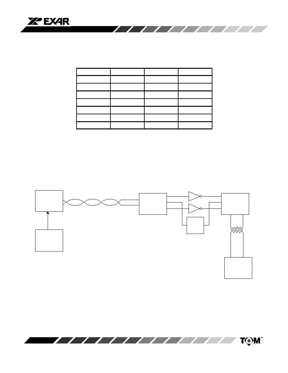
Table 1 shows typical expected jitter tolerance. The
following measurements have been done at a
transmission rate of T1 (1.544MHz). (See
Figure 2).
Jitter
1.544Mbs in UI
Jitter
1.544Mbs in UI
10Hz
>10UI
5kHz
1.3UI
100Hz
>10UI
8kHz
0.8UI
500Hz
>10UI
10kHz
0.7UI
1kHz
6.5UI
32kHz
0.5UI
2kHz
3.3UI
50kHz
0.45UI
3kHz
2.1UI
77kHz
0.45UI
4kHz
1.5UI
-
-
V
CC
= +5V
"
5%, T
A
= 25
∞
C
Table 1. Jitter Tolerance at 1.544Mbps with 6db Cable Loss
TPOS
RPOS
6db Cable Attenuation
Pattern
Generator
HP3781B
Clock
RXDATA-
RXDATA+
XR-T5683A
RX
RCLK
RNEG
XR-T5683A
TX
TCLK
TNEG
Generator
HP3785B
Jitter
TXDATA+
TXDATA-
Figure 2. Jitter Measurement Set-up
(transmitter
side)
Clock
Phase
Shift
Circuit
Jitter
Analyzer
HP3785B
(Receive Side)
XR-T5683A
6
Rev. 2.01
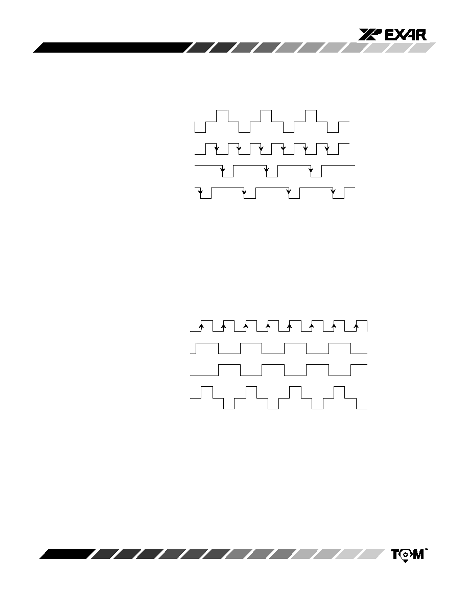
RXDATA+
RCLK Output at Pin 8
RPOS Output at Pin 11
RNEG Output at Pin 10
Figure 3. Receiver Timing Diagram With 1-1-1-1-1-1 Pattern
TCLK Clock to Pin 16
TPOS to Pin 17
Bipolar Signal at Transformer Output
TNEG to Pin 12
Figure 4. Transmitter Input Timing Diagram

XR-T5683A
7
Rev. 2.01
Notes
1
Inputs that are not connected to pulse generator will be tied to V
CC
via 1K resistor.
2
C1 includes probe and jig capacitance.
Figure 5. Test Circuit
100
0.1
µ
F
V
CC
= 5V
Output
CI=15pF
2
0V
Pin 9 & 18
Pin 13 & 15
0V
Pin 7 & 14
8.448MHz
Pulse
Generator
Input
XR-T5683A
Pin 12,16,17
1
Figure 6. Transmitter Test Circuit and Switching Waveforms (Measured at 8.448Mbps)
3V
90%
59ns
<5ns
90%
Input Pulse
From Generator
10%
1.5V
Output From Pin 13
or Pin 15
90%
1.5V
10%
15ns Typ.
15ns Typ.
90%
50%
50%
10%
10%
0V
+5V
Vol
Pulse Width
Rise Time
Fall Time
<5ns
XR-T5683A
8
Rev. 2.01
V
CC
TIP
RING
T1
PE65415
1:1:1
0.1
µ
F
390
RXDATA+
2
RXDATA-
3
BIAS
5
TE
4
TANK BIAS
6
RV
CC
9
RGND
7
RCLK
8
PDC
1
TV
CC
18
TXDATA+
13
TXDATA-
15
TGND
14
RNEG
10
RPOS
11
TNEG
12
TPOS
17
TCLK
16
U1
XR-T5683A
56
TIP
T2
PE65415
1:1:1
RING
56
R
C
L
0.1
µ
F
0.1
µ
F
RNEG
RPOS
TNEG
TPOS
TCLK
V
CC
0.1
µ
F
0.1
µ
F
RCLK
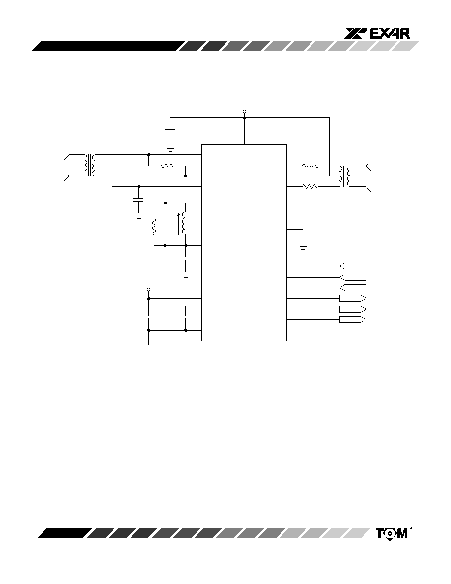
Figure 7. Application Circuit
XR-T5683A
9
Rev. 2.01
INPUT AND OUTPUT TRANSFORMERS
Pulse Engineering types PE-65415, PE-65771 or
PE-65835 transformers, may be used for both the input
and output transformers. These three parts, which are all
1CT:2CT turns ratio and have similar electrical
specifications, are wound on small, epoxy-encapsulated,
torroid cores. They differ in physical size, operating
temperature range and voltage isolation. These
transformers are suitable for operation over the 1.544
through 8.448Mbps range which includes T1, T2, E1 and
E2.
Schott-Part
Number
Nominal
Inductance
Mechanical Style
Bit Rate
(MBIT/S)
Tuning Cap.
(See Note)
24443
48
µ
Hy with CT
RM 5 Core,
4 Pin Bobbin
1.544(T1)
200pF
4 Pin Bobbin
2.048(E1)
100pF
24444
5
µ
Hy with CT
14 x 8 Potcore,
6 Pin Bobbin
6.312(T2)
100pF
6 Pin Bobbin
6.448(E2)
60pF
Table 2. Inductor Selection
Notes
- Capacitor values shown combined with typical stray capacitance will normally resonate the tank circuit at the specific bit rate.
- The center-tapped inductor (L) eliminates clock amplifier overload by reducing the signal amplitude applied to T5683A pin 4. While
feeding pseudo-random data into the receive input, tune this inductor for minimum jitter on the recovered clock (pin 8) as viewed on
an oscilloscope.
- R, which may be in the 20K to 50k
range, is optional and may be used to lower clock recovery circuit Q if desired.
Magnetic Supplier Information:
Pulse
Telecom Product Group
P.O. Box 12235
San Diego, CA 92112
Tel. (619) 674-8100
Fax. (619) 674-8262
John Marshall
Schott Corporation
1838 Elm Hill Pike, Suite 100
Nashville, TN 37210
Tel. (615) 889-8800
Fax (615) 885-0834
XR-T5683A
10
Rev. 2.01
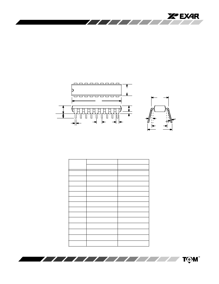
18 LEAD PLASTIC DUAL-IN-LINE
(300 MIL PDIP)
Rev. 1.00
18
1
10
9
D
e
B
1
A
1
E
1
C
E
A
2
L
B
Seating
Plane
SYMBOL
MIN
MAX
MIN
MAX
INCHES
A
0.145
0.210
3.68
5.33
A
1
0.015
0.070
0.38
1.78
A2
0.115
0.195
2.92
4.95
B
0.014
0.024
0.36
0.56
B
1
0.030
0.070
0.76
1.78
C
0.008
0.014
0.20
0.38
D
0.845
0.925
21.46
23.50
E
0.300
0.325
7.62
8.26
E
1
0.240
0.280
6.10
7.11
e
0.100 BSC
2.54 BSC
e
A
0.300 BSC
7.62 BSC
e
B
0.310
0.430
7.87
10.92
L
0.115
0.160
2.92
4.06
0
∞
15
∞
0
∞
15
∞
MILLIMETERS
A
Note: The control dimension is the inch column
e
B
e
A
XR-T5683A
11
Rev. 2.01
SYMBOL
MIN
MAX
MIN
MAX
A
0.093
0.104
2.35
2.65
A
1
0.004
0.012
0.10
0.30
B
0.013
0.020
0.33
0.51
C
0.009
0.013
0.23
0.32
D
0.447
0.463
11.35
11.75
E
0.291
0.299
7.40
7.60
e
0.050 BSC
1.27 BSC
H
0.394
0.419
10.00
10.65
L
0.016
0.050
0.40
1.27
0
∞
8
∞
0
∞
8
∞
INCHES
MILLIMETERS
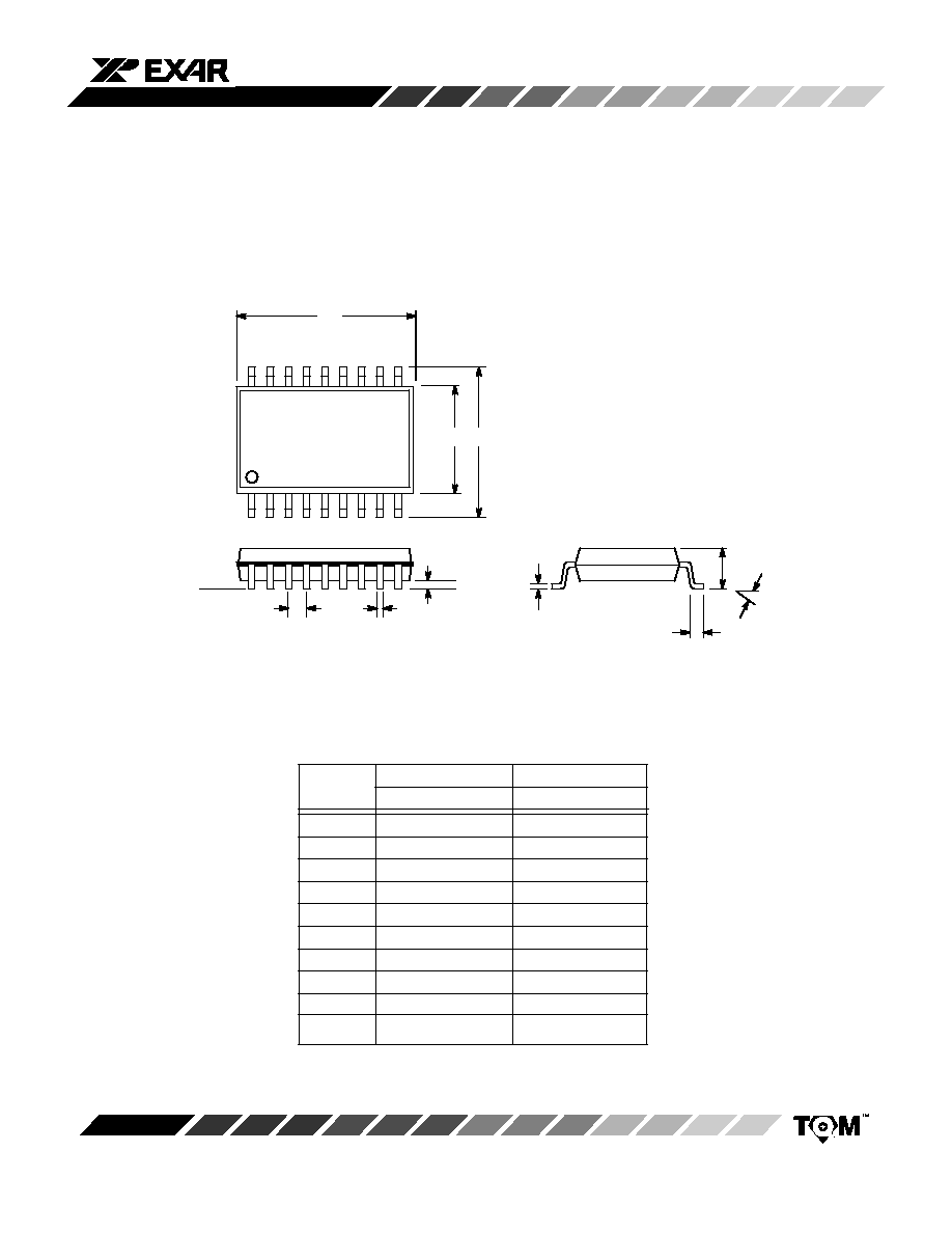
18 LEAD SMALL OUTLINE
(300 MIL JEDEC SOIC)
Rev. 1.00
e
18
10
9
D
E
H
B
A
L
C
A
1
Seating
Plane
Note: The control dimension is the millimeter column
1

XR-T5683A
12
Rev. 2.01
NOTICE
EXAR Corporation reserves the right to make changes to the products contained in this publication in order to im-
prove design, performance or reliability. EXAR Corporation assumes no responsibility for the use of any circuits de-
scribed herein, conveys no license under any patent or other right, and makes no representation that the circuits are
free of patent infringement. Charts and schedules contained herein are only for illustration purposes and may vary
depending upon a user's specific application. While the information in this publication has been carefully checked;
no responsibility, however, is assumed for inaccuracies.
EXAR Corporation does not recommend the use of any of its products in life support applications where the failure or
malfunction of the product can reasonably be expected to cause failure of the life support system or to significantly
affect its safety or effectiveness. Products are not authorized for use in such applications unless EXAR Corporation
receives, in writing, assurances to its satisfaction that: (a) the risk of injury or damage has been minimized; (b) the
user assumes all such risks; (c) potential liability of EXAR Corporation is adequately protected under the circum-
stances.
Copyright 1995 EXAR Corporation
Datasheet June 1997
Reproduction, in part or whole, without the prior written consent of EXAR Corporation is prohibited.