Document Outline
- Main Menu
- Products
- XRT5894 Menu
- Alphanumeric Index
- Search

XRT5894
Four-Channel E1
Line Interface (3.3V or 5.0V)
Rev. 1.10
E
2000
EXAR Corporation, 48720 Kato Road, Fremont, CA 94538 z (510) 668-7000 z FAX (510) 668-7017
March 2000-3
FEATURES
D
Compliant with ITU G.703 Pulse Mask Template for
2.048Mbps (E1) Rates
D
Four Independent CEPT Transceivers
D
Supports Differential Transformer Coupled
Receivers and Transmitters
D
On Chip Pulse Shaping for Both 75W and 120W Line
Drivers
D
Compliant with ITU G.775 LOS Declaration/Clearing
Recommendation
D
Optional User Selectable LOS Declaration/Clearing
Delay
D
Logical Inputs Accept either 3.3V or 5.0V Levels
D
Ultra-Low Power Dissipation
D
+3.3V or 5.0V Supply Operations
D
Individual Transmit Channel Over Temperature
Protection
APPLICATIONS
D
SDH Multiplexer
D
Digital Cross Connects
GENERAL DESCRIPTION
The XRT5894 is an optimized four channel 3.3V line
interface unit fabricated using low power CMOS
technology. The device contains four independent E1
channels. Each channel performs the driver and receiver
functions necessary to convert bipolar signals to logical
levels and vice versa. The device requires transformers
on both receiver and transmitter sides, and supports both
balanced and unbalanced interfaces.
The device offers two distinct modes of LOS detection.
The first method, which does not require an external
clock, provides an LOS output indication signal with
thresholds and delay that comply with the ITU G.775
requirements. In the second mode, the user provides an
external clock that increases the delay for LOS
declaration and clearing. This feature provides the user
with the flexibility to implement LOS specifications that
require a delay greater than the G.775 requirements.
ORDERING INFORMATION
Part No.
Package
Operating
Temperature Range
XRT5894IV
64 Lead TQFP (10 x 10 x 1.4mm)
-40�C to +85�C
XRT5894
2
Rev. 1.10
To
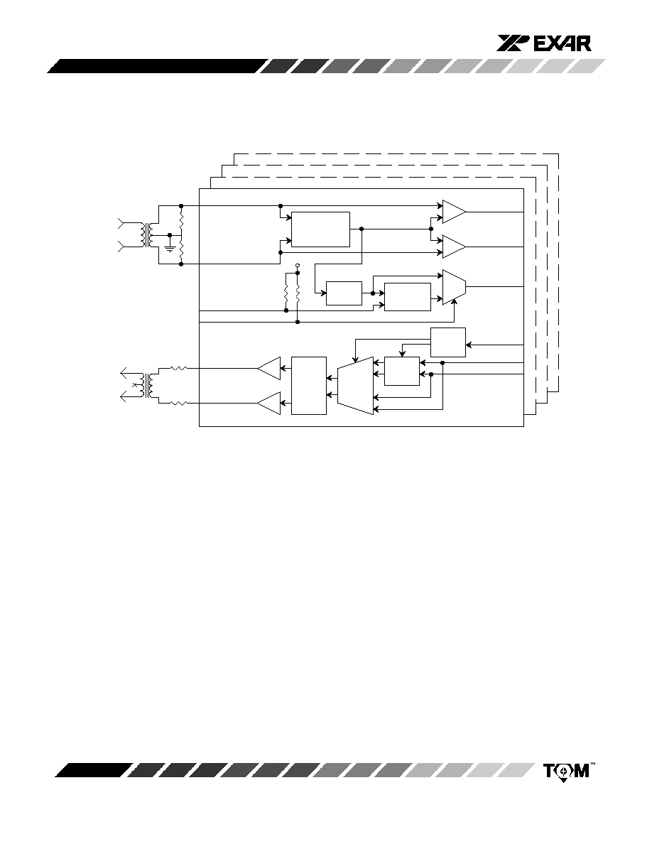
BLOCK DIAGRAM
Figure 1. XRT5894 Block Diagram
RTIP4 (43)
RRING4 (42)
LOSSEL (25)
TXCLK4 (51)
TTIP4 (53)
TRING4 (55)
LOS4 (48)
TXPOS4 (49)
TXNEG4 (50)
RXNEG4 (46)
RXPOS4 (47)
LOSCNT (45)
Signal
Peak
LOS
Detect
Loss
Delay
Mux
O
Pulse
Shaping
NRZ
Duty
Cycle
Mux
0
2:1
1:2
R1
RING
RING
TIP
RX Input
TIP
TX OUTPUT
Receive
Comparators
Line
Drivers
R2
R3
9.1
R4
9.1
Transceiver 2
Transceiver 1
Transceiver 3
Tranceiver 4
Detector
Counter
1
RZ
Adjust
0
1
1
Transmit
V
CC
Receiver Notes
D
The same type 1:2CT ratio transformer may be
used at the receiver input and transmitter output.
D
R1 and R2 are both 150W for 75W operation, or
240W for 120W operation.
D
Return loss exceeds ITU G.703 specification with
these resistors and a 1:2CT ratio input transformer.
LOS (Loss of Signal) Notes
D
LOSSEL (pin 25) is connected to logic "1" for ITU
G.775 compliant LOS delay, or to logic 0 for user
programmable additional delay.
D
LOSCNT (pin 45) is unconnected when LOSSEL is
logic 1, or connected to an external clock when
LOSSEL is logic 0.
Transmitter Notes
D
Return loss exceeds ETSI 300 166 specification
with a 1:2 ratio transformer.
D
R3 and R4 are always 9.1W for both 75W and 120W
applications.
XRT5894
3
Rev. 1.10
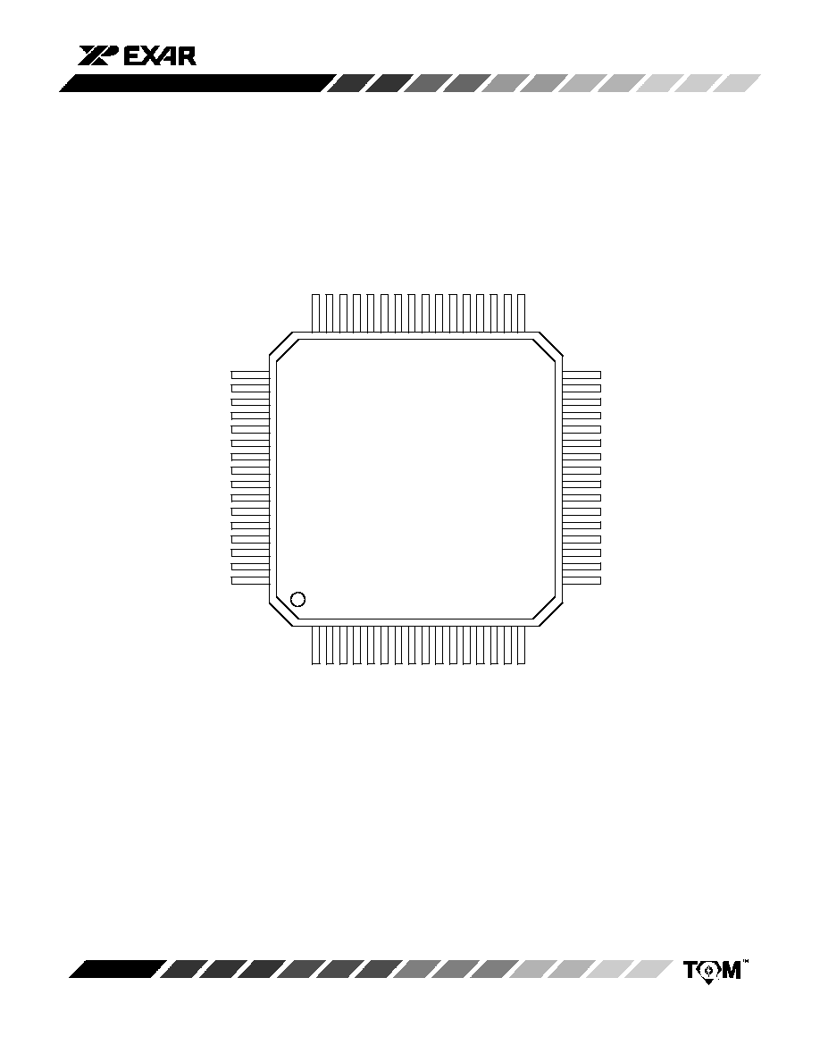
PIN CONFIGURATION
48
33
32
17
1
16
49
64
64 LEAD THIN QUAD FLAT PACK
(10 x 10 x 1.4 mm, TQFP)
L
O
S
1
R
X
P
O
S
1
R
X
N
E
G
1
V
C
C
R
T
I
P
1
R
R
I
N
G
1
G
N
D
V
C
C
V
C
C
G
N
D
T
R
I
N
G
2
V
C
C
T
T
I
P
2
G
N
D
R
T
I
P
2
R
R
I
N
G
2
TXCLK2
TXNEG2
TXPOS2
LOS2
RXPOS2
RXNEG2
V
CC
NC
LOSSEL
GND
RXNEG3
RXPOS3
LOS3
TXPOS3
TXNEG3
TXCLK3
R
R
I
N
G
3
R
T
I
P
3
G
N
D
T
T
I
P
3
V
C
C
T
R
I
N
G
3
G
N
D
V
C
C
G
N
D
R
R
I
N
G
4
R
T
I
P
4
GND
G
N
D
L
O
S
C
N
T
R
X
N
E
G
4
R
X
P
O
S
4
L
O
S
4
TXPOS4
TXNEG4
TXCLK4
TTIP4
V
CC
TRING4
GND
GND
TRING1
V
CC
TTIP1
GND
TXCLK1
TXNEG1
TXPOS1

XRT5894
4
Rev. 1.10
PIN DESCRIPTION
Pin #
Symbol
Type
Description
1
LOS1
O
Receiver 1 Loss of Signal.
Asserted during LOS condition.
2
RXPOS1
O
Receiver 1 Positive Data Out.
Positive RZ data output for channel 1.
3
RXNEG1
O
Receiver 1 Negative Data Out.
Negative RZ data output for channel 1.
4
V
CC
Positive Supply (+3.3V or +5.0V + 5%).
Digital circuitry.
5
RTIP1
I
Receiver 1 Positive Bipolar Input.
6
RRING1
I
Receiver 1 Negative Bipolar Input.
7
V
CC
Positive Supply (+3.3V or +5.0V + 5%).
Analog circuitry.
8
GND
Analog Ground.
9
V
CC
Positive Supply. (+3.3V or +5.0V + 5%).
Analog circuitry.
10
GND
Analog Ground.
11
TRING2
O
Transmitter 2 Negative Bipolar Output.
12
V
CC
Positive Supply (+3.3V or +5.0V + 5%
). Transmitter channel 2.
13
TTIP2
O
Transmitter 2 Positive Bipolar Output.
14
GND
Analog Ground.
Transmitter channel 2.
15
RTIP2
I
Receiver 2 Positive Bipolar Input.
16
RRING2
I
Receiver 2 Negative Bipolar Input.
17
TXCLK2
I
Transmitter 2 Clock Input.
Use for clocked mode with NRZ data.
1
18
TXNEG2
I
Transmitter 2 Negative Data Input.
Negative NRZ or RZ data input.
1
19
TXPOS2
I
Transmitter 2 Positive Data Input.
Positive NRZ or RZ data input.
1
20
LOS2
O
Receiver 2 Loss of Signal.
Asserted during LOS condition.
21
RXPOS2
O
Receiver 2 Positive Data Out.
Positive RZ data output for channel 2.
22
RXNEG2
O
Receiver 2 Negative Data Out.
Negative RZ data output for channel 2.
23
V
CC
Positive Supply (+3.3V or +5.0V + 5%).
Digital circuitry.
24
NC
No Connect.
25
LOSSEL
I
Loss of Signal Delay Select.
"Hi" selects G.775, "Lo" selects user programmable.
1
26
GND
Digital Ground.
27
RXNEG3
O
Receiver 3 Negative Data Out.
Negative RZ data output for channel 3.
28
RXPOS3
O
Receiver 3 Positive Data Out.
Positive RZ data output for channel 3.
29
LOS3
O
Receiver 3 Loss of Signal.
Asserted during LOS condition.
30
TXPOS3
I
Transmitter 3 Positive Data Input.
Positive NRZ or RZ data input.
1
31
TXNEG3
I
Transmitter 3 Negative Data Input.
Negative NRZ or RZ data input.
1
32
TXCLK3
I
Transmitter 3 Clock Input.
Use for clocked mode with NRZ data.
1
33
RRING3
I
Receiver 3 Negative Bipolar Input.
34
RTIP3
I
Receiver 3 Positive Bipolar Input.
Note:
1
Has internal pull-up 50KW resistor.

XRT5894
5
Rev. 1.10
PIN DESCRIPTION (CONT'D)
Pin #
Symbol
Type
Description
35
GND
Analog Ground.
36
TTIP3
O
Transmitter 3 Positive Bipolar Output.
37
V
CC
Positive Supply (+3.3V or +5.0V + 5%
). Transmitter channel 3.
38
TRING3
O
Transmitter 3 Negative Bipolar Output.
39
GND
Analog Ground.
Transmitter channel 3.
40
V
CC
Positive Supply (+3.3V or +5.0V + 5%
). Analog circuitry.
41
GND
Analog Ground.
42
RRING4
I
Receiver 4 Negative Bipolar Input.
43
RTIP4
I
Receiver 4 Positive Bipolar Input.
44
GND
Analog Ground.
45
LOSCNT
I
Loss of Signal Timing Clock Input.
For user--programmable LOS delay.
1
46
RXNEG4
O
Receiver 4 Negative Data Out.
Negative RZ data output for channel 4.
47
RXPOS4
O
Receiver 4 Positive Data Out.
Positive RZ data output for channel 4.
48
LOS4
O
Receiver 4 Loss of Signal.
Asserted during LOS condition.
49
TXPOS4
I
Transmitter 4 Positive Data Input.
Positive NRZ or RZ data input.
1
50
TXNEG4
I
Transmitter 4 Negative Data Input.
Negative NRZ or RZ data input.
1
51
TXCLK4
I
Transmitter 4 Clock Input.
Use for clocked mode with NRZ data.
1
52
GND
Analog Ground.
Transmitter channel 4.
53
TTIP4
O
Transmitter 4 Positive Bipolar Output.
54
V
CC
Positive Supply (+3.3V or +5.0V + 5%
). Transmitter channel 4.
55
TRING4
O
Transmitter 4 Negative Bipolar Output.
56
GND
Digital Ground.
57
GND
Analog Ground.
58
TRING1
O
Transmitter 1 Negative Bipolar Output.
59
V
CC
Positive Supply (+3.3V or +5.0V + 5%
). Transmitter channel 1.
60
TTIP1
O
Transmitter 1 Positive Bipolar Output.
61
GND
Analog Ground.
Transmitter channel 1.
62
TXCLK1
I
Transmitter 1 Clock Input.
Use for clocked mode with NRZ data.
1
63
TXNEG1
I
Transmitter 1 Negative Data Input.
Negative NRZ or RZ data input.
1
64
TXPOS1
I
Transmitter 1 Positive Data Input.
Positive NRZ or RZ data input.
1
Note:
1
Has internal pull-up 50KW resistor.

XRT5894
6
Rev. 1.10
ELECTRICAL CHARACTERISTICS
Test Conditions: V
CC
= 3.3V or 5.0V
+ 5%, T
A
= -40 to 25 to 85�C, Unless Otherwise Specified
Symbol
Parameter
Min.
Typ.
Max.
Unit
Conditions
DC Electrical Characteristics
Parameters
V
CC
Voltage Supply
3.135
3.3
3.465
V
3.3V Operation
V
CC
Voltage Supply
4.75
5.0
5.25
V
5V Operation
Inputs
V
IH
Input High Level
2.0
5.0
V
V
IL
Input Low Level
0.8
V
Outputs
V
OH
Output High Level
2.4
V
I
OH
= -4mA
V
OL
Output Low Level
0.4
V
I
OL
= 4mA
Receiver Specifications
RX
CL
Allowable Cable Loss
0
10
12
dB
Cable loss at 1.024MHz (Relative
to 0dB = 2.37Vp measured from
RTIP or RRING to ground).
RX
IM
Interference Margin
-15
-12
dB
With 6dB cable loss
RX
XI
Receiver Slicing Threshold
45
50
55
%
% of peak input voltage at -3dB
cable loss
RX
LOSSET
LOS Must Be Set If RX Sig.
Atten.
�
32dB (For Any Valid
Data Pattern)
15
32
dB
Relative to 0dB = 2.37Vp
Measured from RTIP or RRING to
ground.
RX
LOSCLR
LOS Must Be Cleared If RX Sig.
Atten. < 9dB
9
12
dB
Relative to 0dB = 2.37Vp
measured from RTIP or RRING to
ground.
RX
LOSHYST
Hysteresis on Input Data
1
dB
For LOS output state change
RX
IN
Input Impedance
5
kW
Up to 3.072MHz (Measured from
RTIP or RRING to ground).
Power Specifications V
CC
= 3.3V
P
D
Power Dissipation
460
590
mW
All 1's Transmit and Receive 75W
P
D
Power Dissipation
117
155
mW
All Drivers Power Down
P
C
Power Consumption 75W
770
900
mW
All 1's Transmit and Receive
P
C
Power Consumption 75W
555
675
mW
50% data density, Transmit and Re-
ceive
P
C
Power Consumption 120W
635
780
mW
All 1's Transmit and Receive
P
C
Power Consumption 120W
475
605
mW
50% data density, Transmit and Re-
ceive
Power Specifications V
CC
= 5.0V
P
D
Power Dissipation
945
1240
mW
All 1's Transmit and Receive 75W
P
D
Power Dissipation
235
290
mW
All Drivers Power Down
P
C
Power Consumption 75W
1250
1555
mW
All 1's Transmit and Receive
Note:
Bold face parameters are covered by production test and guaranteed over operating temperature range.

XRT5894
7
Rev. 1.10
ELECTRICAL CHARACTERISTICS
(CONT'D)
Test Conditions: V
CC
= 3.3V or 5.0V
+ 5%, T
A
= -40 to 25 to 85�C, Unless Otherwise Specified
Symbol
Parameter
Min.
Typ.
Max.
Unit
Conditions
Power Specifications V
CC
=5.0V (Cont'd)
P
C
Power Consumption 120W
1075
1345
mW
All 1's Transmit and Receive
P
C
Power Consumption 75W
1025
1300
mW
50% data density, Transmit and Re-
ceive
P
C
Power Consumption 120W
940
1220
mW
50% data density, Transmit and Re-
ceive
AC Electrical Characteristics
V
TXOUT
Output Pulse Amplitude
(R
L
= 75W)
2.13
2.37
2.60
V
Trans. = 1:2 ratio, 9.1W in series
with each end of primary
V
TXOUT
Output Pulse Amplitude
(R
L
= 120W)
2.70
3.0
3.30
V
Trans. = 1:2 ratio, 9.1W in series
with each end of primary
T
XPW
Output Pulse Width
224
244
264
ns
PN
IMP
Pos/Neg Pulse Unbalanced
5
%
T
1
TXCLK Clock Period (E1)
488
ns
T
2
TXCLK Duty Cycle
30
50
70
%
T
SU
Data Set-up Time, TDATA to
TXCLK
75
ns
50% TXCLK Duty Cycle
T
HO
Data Hold Time, TDATA to
TXCLK
30
ns
50% TXCLK Duty Cycle
T
R
TXCLK Rise Time (10% to 90%)
40
ns
T
F
TXCLK Fall Time (10% to 90%)
40
ns
T
3-noclk
Data Prop. Delay No-Clock
Mode
35
50
ns
T
3-clk
Data Prop. Delay Clock Mode
470
ns
50% TXCLK Duty Cycle
T
4
Receive Data High
219
244
269
ns
0dB Cable Loss
T
5
RX Data Prop. Delay
40
ns
15pF Load
T
6
Receive Rise Time
40
ns
15pF Load
T
7
Receive Rise Time
40
ns
15pF Load
Note:
Bold face parameters are covered by production test and guaranteed over operating temperature range.
ABSOLUTE MAXIMUM RATINGS
Storage Temperature
-65�C to +150�C
. . . . . . . . . . . .
Operating Temperature
-40�C to +85�C
. . . . . . . . . .
Supply Voltage
-0.3V to +6.0V
. . . . . . . . . . . . . . . . . . .
ESD Protection
>1000V (HBM)
. . . . . . . . . . . . . . . . . .

XRT5894
8
Rev. 1.10
Disabling Output Drivers
Output drivers may be individually disabled (hi-z output) by either of the following methods.
1. Either connect the transmit data inputs TXPOS
and TXNEG for the channel to be disabled to a log-
ic 1 source (VCC), or allow them to float (inputs
have internal pull--up resistors).
2. Connect TXCLK for the channel to be disabled to
logic 0 source (Ground), and also apply data to the
TXPOS and TXNEG inputs of that channel.
TRANSFORMER REQUIREMENTS
Turns Ratio
Line Impedance
1:2 CT
75W or 120W
Table 1. Input Transformer Requirements
Turns Ratio
Line Impedance
1:2
75W or 120W
Table 2. Output Transformer Requirements
Note:
The same type 1:2 CT ratio device may be used at both receiver input and transmitter output.
The following transformers have been tested with the
XRT5894:
HALO type TG26-1205(package contains two 1 CT:2 CT ratio transformers)
Pulse type PE-65535 (1:2 CT ratio)
Transpower Technologies type TTI 7154-R (1:2 CT ratio)
Magnetic Supplier Information:
HALO Electronics, Inc.
P.O. Box 5826
Redwood City, CA 94063
Tel. (415) 568-5800
Fax. (415)568-6161
Pulse
Telecom Product Group
P.O. Box 12235
San Diego, CA 92112
Tel. (619) 674-8100
Fax. (619) 674-8262
Transpower Technologies, Inc.
24 Highway 28, Suite 202
Crystal Bay, NV 89402--0187
Tel. (702) 831--0140
Fax. (702) 831--3521

XRT5894
9
Rev. 1.10
TXOUT (n)
TXCLK (n)
TXNEG (n)
TXPOS (n)
TSU
THO
TSU
THO
T1
T2
TR
TF
T3
VTXOUT
TXPW
VTXOUT
TXPW
T3
RXIN (n)
RPOS (n)
RXNEG (n)
T5
T4
T5
T4
T6
T7
T6
T7
Figure 2. Transmit Timing Diagram
Figure 3. Receive Timing Diagram
XRT5894
10
Rev. 1.10
RETURN LOSS SPECIFICATIONS
The following transmitter and receiver return loss specifications are based on a typical 1:2CT ratio transformer.
75W
120W
Frequency Range
Min.
Typ.
Min.
Typ.
Unit
51kHz to 102kHz
16
22
10
15
dB
102kHz to 2.048MHz
16
22
10
15
dB
2.048MHz to 3.072MHz
11
18
10
14
dB
Table 3. Transmitter Return Loss Specification
Transmit Return Loss Notes
D
Output transformer ratio is 1:2 (return loss exceeds
ETSI 300 166 with this transformer).
D
For both 75
W
and 120
W
applications, 9.1
W
, 1% re-
sistors are connected between each end of the
transformer primary and the XRT5894 TTIP and
TRING pins.
75W
120W
Frequency Range
Min.
Typ.
Min.
Typ.
Unit
51kHz to 102kHz
16
28
15
18
dB
102kHz to 2.048MHz
22
34
22
25
dB
2.048MHz to 3.072MHz
18
26
20
30
dB
Table 4. Receiver Return Loss Specification
Receiver Return Loss Notes
D
Input transformer ratio is 1:2 CT.
D
Transformer center tap is grounded.
D
Each half of transformer secondary is terminated
with 150
W
for 75
W
operation, or 240
W
for 120
W
op-
eration (resistors are 1% tolerance).

XRT5894
11
Rev. 1.10
SYSTEM DESCRIPTION
This device is a four channel E1 transceiver that provides
an electrical interface for 2.048Mbps applications. Its
unique architecture includes four receiver circuits that
convert ITU G.703 compliant bipolar signals to TTL
compatible logic levels. Each receiver includes a LOS
(Loss of Signal) detection circuit that may be configured
for either a fixed or a user-programmable LOS response
time delay. Similarly, in the transmit direction, four
transmitters convert TTL compatible logic levels to G.703
compatible bipolar signals. Each transmitter may be
operated either with RZ, or NRZ data types. In NRZ mode
a transmit clock is required as well. The following
description applies to any of the four receivers or
transmitters contained in the XRT5894. Therefore, the
suffix numbers for a particular channel are deleted for
simplicity. i.e. "RTIP" applies to RTIP1 through RTIP4.
Receiver Operation
A bipolar signal is transformer-coupled to the receiver
differential inputs (RTIP and RRING). The receiver is able
to tolerate up to 12dB of line loss measured at 1.024MHz.
It contains slicing circuitry that automatically samples the
incoming data at a fixed percentage (50% nominal) of the
peak signal amplitude. A precision peak detector
maintains the slicing level accuracy. The TTL compatible
receiver output data rails appear at the RXPOS and
RXNEG pins. The pulse width of this data; which is in RZ
format, is a function of the amount of the cable loss
present.
Receiver Loss Of Signal Detection (LOS)
Absence of signal at any receiver input is detected by the
loss of signal (LOS) circuit. One LOS detection circuitry is
provisioned for each receiver. The LOS signal is asserted
(LOS=1) when a LOS condition is detected and is cleared
(LOS=0) when a valid input signal is restored.
Two modes of LOS circuit operation are supported.
These distinct modes are called "automatic" and
"user-programmable". When LOSSEL (pin 25) is set to
logic "1", the automatic mode is selected. In this mode the
LOS condition will be declared and cleared in full
compliance with ITU G.775 specification. When LOSSEL
is connected to logic "0", the user-programmable delay
mode is enabled. In this mode the user has the option of
extending the delay of LOS declaration and clearing
specified in the ITU G.775. This is done by providing a
user-supplied clock to LOSCNT (pin 45). The "user
programmable mode" is provisioned to allow systems
designers to comply with older versions of LOS
specifications in legacy systems. It needs to be stressed
that the delay for declaration and clearing of the LOS
condition will never be less than the range specified in the
G.775 specification (10-255 pulse intervals).
The LOS detection/clearing circuitry of the XRT5894 in
"automatic" mode will detect LOS when the incoming
signal has "no transitions" i.e. when the signal level is less
than or equal to a signal level A
D
dB below nominal signal
level, for N consecutive pulse intervals, where 10<N<255.
The value of A
D
can vary between 10dB to 32dB
depending on the ones density of the incoming signal
assuming the received data has minimum permissible
ones density. Furthermore LOS detect is cleared when
the incoming signal has "transitions," i.e. when the signal
level is greater than or equal to a signal level of A
C
dB
below nominal, for N consecutive pulse intervals, where
10<N<255. The value of A
C
can vary between 9dB to
31dB depending on the ones density of the incoming
signal assuming the received data has minimum
permissible ones density. Each pulse interval is 488ns at
E1 rates. The absolute value of A
C
is always smaller than
A
D
by at least 1dB.
The LOS detection/clearing criteria described above is
fully compliant with G.775 LOS specification. In the "user
programmable" mode the user has the option of
extending the declaration and clearing delay (10<N<255)
by an amount which is equal to 2048 x T. T is the time
period of the clock supplied to LOSCNT (pin 45) by the
user.
Nominal signal level is defined as 2.37V peak measured
between RTIP or RRING and ground. (This voltage will
be present in 75W applications using a 1:2 CT ratio input
transformer terminated in 300W with the center tap
grounded with 0dB of cable and a 2.37V peak amplitude
transmit pulse at the cable input.)
Transmitters
This device contains four identical ITU G.703 compliant
transmitters. The output stage of each transmitter is a
differential voltage driver. External resistors need to be
connected to the primary of output transformer. This is
necessary to maintain an accurate source impedance
XRT5894
12
Rev. 1.10
that ensures compliance to ETSI 300 166 return loss
requirement.
TTL compatible dual rail transmit data signals are
supplied to TXPOS and TXNEG inputs. The transmitter
differential outputs TTIP and TRING are connected to the
output transformer primary through series 9.1W resistors.
All the four transmitters can be operated in two distinct
modes of operation referred to as "clocked" or "clockless"
modes. The operational mode is selected automatically
based on the signal provided to TXCLK input. If a clock is
present at this pin, the transmitter detects its presence
and operates in the clocked mode. In this mode, the
transmit input should be supplied with full-width NRZ
pulses. If a clock is not present at the TXCLK input (pin is
left open), the part operates in the clockless mode. In this
mode, RZ data should be supplied to the device. Each
transmit channel of XRT5894 has a duty cycle correction
circuitry. This enables the device to produce output
bipolar pulses fully compliant with G.703 despite having
TXCLK signal with 30% to 70% duty cycle.
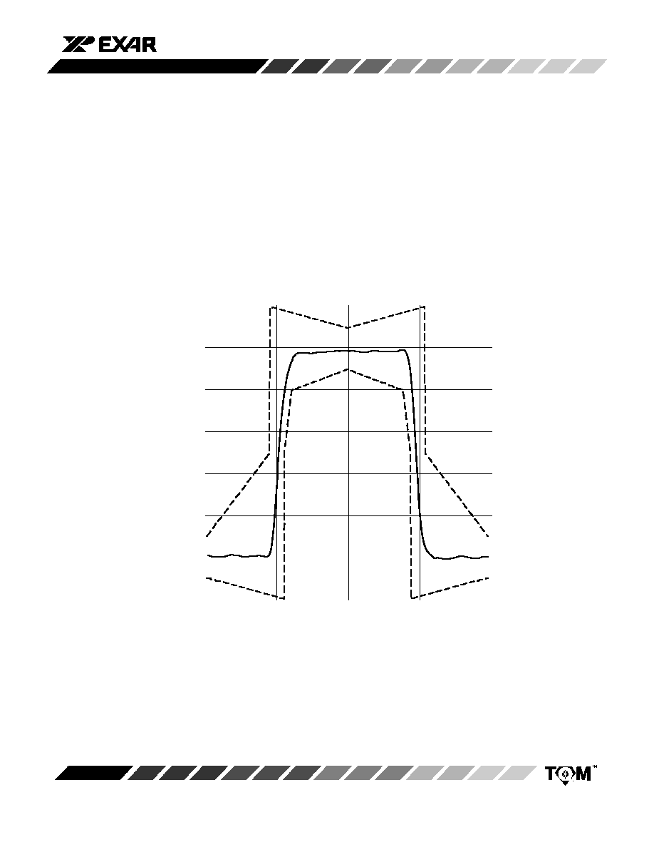
Figure 4. CCITT G.703 Pulse Template
20%
488 ns
(244 + 244)
219 ns
(244 -- 25)
0%
50%
V = 100%
269 ns
(244 + 25)
194 ns
(244 -- 50)
Nominal pulse
244 ns
10%
10%
10%
10%
10%
10%
20%
20%
Note: V corresponds to the nominal peak value
XRT5894
13
Rev. 1.10
Transmitter Output Pulse Measurement
Figure 5
shows a typical transmit pulse plotted on the template shown in ITU G.703 Figure 15/G.703. The following
conditions apply:
V
CC
=3.30V
Transmitter output transformer secondary terminated with 120W
All ones signal
Receiver output looped backed into transmitter digital input
Operation without transmitter clock (RZ data)
Measurement made with a Tektronix TDS640 digital scope set to full bandwidth
1.2
1.0
0.8
0.6
0.4
0.2
0
-0.2
-244
-122
0
122
244
Time (ns)
N
o
r
m
a
l
i
z
e
d
A
m
p
l
i
t
u
d
e
Figure 5. XRT5894 Output Pulse
XRT5894
14
Rev. 1.10
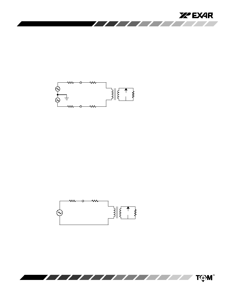
Transmitter Output Return Loss Measurements
The following measurements were made with a Wandel
and Goltermann SNA--2 Network Analyzer equipped with
an RFZ--1 75W Return Loss Bridge. A 75W to 120W
impedance matching transformer was used to make the
120W measurement. A network analyzer calibration run
subtracted out the effects of this transformer.
Test Conditions:
D
Output transformer ratio was 1:2.
D
Transmitter series resistors (R3 and R4 in Figure 1)
were 9.1W .
D
Device was powered from a 3.3V source, transmitter
was enabled, and no output data was present.
This configuration was used for both 75W and 120W
measurements. The only change was the termination
resistance provided by the return loss bridge.
Test Results:
Table 5
compares measured output return loss with
requirements in ETSI FINAL DRAFT prETS 300 166,
June 1993. These results show that measured return loss
is mainly determined by the characteristics of the output
transformer. This is particularly evident for the 120W load
where the measured result is better than the calculated
value.
Specified
Frequency
Frequency
(KHz)
ETSI Spec.
(Min. dB)
Meas. Value (dB)
75W Load
Meas. Value (dB)
120W Load
0.025 fb
51.2
6
22.6
15.4
0.05 fb
102.4
8
22.6
15.7
1.5 fb
3072
8
18.0
14.6
Table 5. Transmitter Output Return Loss Measurements
Notes:
fb = 2048KHz
This data shows that the XRT5894 is fully compliant with the ETSI Output Return Loss Specification for E1 operation with either
75W or 120W loads.

XRT5894
15
Rev. 1.10
The following pictures show typical results of measurements that made over a 50 KHz to 3.5MHz frequency range.
Figure 6. 75W Return Loss Measurement
Figure 6
shows a return loss better than 20dB at low frequencies that decreases to about 12dB at 3.5MHz. Since the
source and load resistances are well--matched, the return loss degradation is due to the transformer.
Figure 7. 120W Return Loss Measurement
Figure 7
shows that for the 120W case, transformer characteristics improve return loss at lower frequencies. At 3.5 MHz,
return loss is close to the calculated 13.8dB for a 75W source terminated with 120W.
XRT5894
16
Rev. 1.10
Output Transformer Selection
A 1:2 ratio transformer is recommended for both 75W and 120W operation because the transmitter, when equipped with
this device, meets both the ITU G.703 output pulse amplitude requirement and, the ETSI return loss specification.
Although a center--tapped output transformer is not required, choosing a part with a center-tapped secondary allows the
use of the same type of unit at the receiver input.
A theoretical justification for the 1:2 ratio transformer follows:
Figure 8. Transmitter Line Driver Model
VS
pos
VS
neg
RS
neg
TRING
R4
R
L
R3
RS
pos
V
O
TTIP
1:n
Where:
Vs
pos
= Vs
neg
= 1.25V typical (Differential line driver peak output voltage swing)
Rs
pos
= Rs
neg
= 0.8W typical (Differential line driver internal source resistance)
R3 = R4 = 9.1W (Differential line driver external source resistance from Figure 1)
R
L
= 75W or 120W (Transmitter load resistance)
n = 2 (Transformer turns ratio)
Vo = Transmitter peak output voltage (Measured across R
L
= 75W or R
L
= 120W )
Figure 9
may be converted to a single--ended model:
Figure 9. Single-ended Line Driver Model
R
L
RS
ext
RS
int
1:n
V
O
V
S
Where:
VS = �Vs
pos
� + �Vs
neg
�
RS
int
= RS
pos
+ Rs
neg
RS
ext
= R3 + R4

XRT5894
17
Rev. 1.10
This may be further simplified:
Figure 10. Equivalent Circuit
V
eq
V
s
R
T
I
Where:
R
T
= RS
int
+ Rs
ext
R
eq
=
R
L
n
2
Therefore:
I =
Vs
R
T
+ Req
V
eq
= I R
eq
V
o
= n V
eq
And:
Return Loss = 20 log
R
T
+ R
eq
R
T
-- R
eq
Table 5
contains the results of calculations made with these equations. The numbers show that output pulse amplitude
is within millivolts of the nominal values of 2.37V and 3.00V specified by ITU G.703 for 75W and 120W operation. Also,
the 1:2 ratio transformer provides an almost-perfect match for 75W operation, and return loss is well within the ETSI
specification for the 120W load.
Load Resistance
R
L
(W)
Pulse Amplitude
Vo (Volts Peak)
Output
Return Loss (dB)
75
2.43
31.3
120
3.01
13.8
Table 5. Calculated Transmitter Pulse Amplitude and Return Loss
XRT5894
18
Rev. 1.10
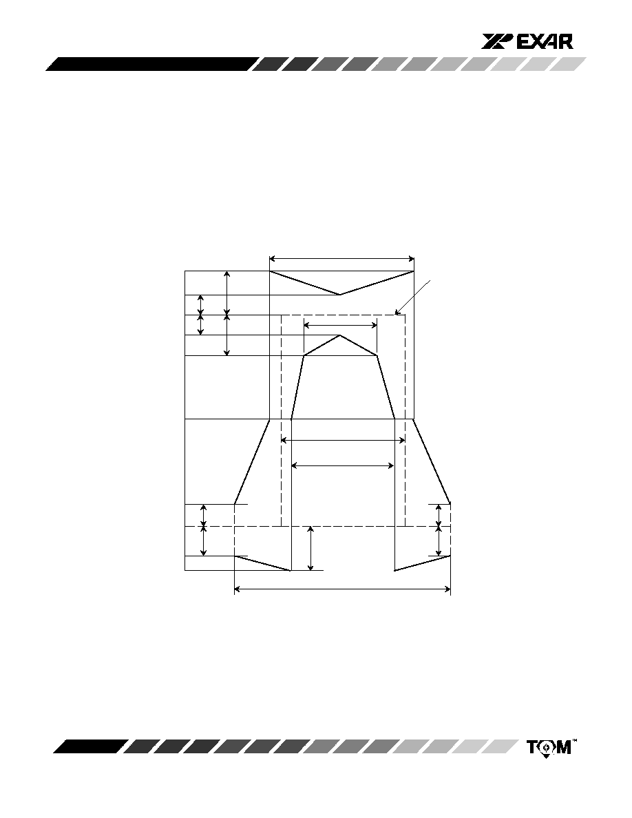
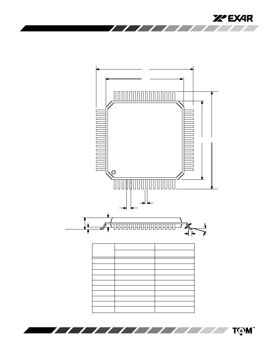
A
0.055
0.063
1.40
1.60
A
1
0.002
0.006
0.05
0.15
A
2
0.053
0.057
1.35
1.45
B
0.005
0.009
0.13
0.23
C
0.004
0.008
0.09
0.20
D
0.465
0.480
11.80
12.20
D
1
0.390
0.398
9.90
10.10
e
0.020 BSC
0.50 BSC
L
0.018
0.030
0.45
0.75
a
0
�
7
�
0
�
7
�
64 LEAD THIN QUAD FLAT PACK
(10 x 10 x 1.4 mm, TQFP)
Rev. 2.00
SYMBOL
MIN
MAX
MIN
MAX
INCHES
MILLIMETERS
48
33
32
17
1
16
49
64
D
D
1
D
D
1
B
e
A
2
a
A
1
A
Seating Plane
Note: The control dimension is the millimeter column
L
C

XRT5894
19
Rev. 1.10
NOTICE
EXAR Corporation reserves the right to make changes to the products contained in this publication in order to im-
prove design, performance or reliability. EXAR Corporation assumes no responsibility for the use of any circuits de-
scribed herein, conveys no license under any patent or other right, and makes no representation that the circuits are
free of patent infringement. Charts and schedules contained herein are only for illustration purposes and may vary
depending upon a user's specific application. While the information in this publication has been carefully checked;
no responsibility, however, is assumed for inaccuracies.
EXAR Corporation does not recommend the use of any of its products in life support applications where the failure or
malfunction of the product can reasonably be expected to cause failure of the life support system or to significantly
affect its safety or effectiveness. Products are not authorized for use in such applications unless EXAR Corporation
receives, in writing, assurances to its satisfaction that: (a) the risk of injury or damage has been minimized; (b) the
user assumes all such risks; (c) potential liability of EXAR Corporation is adequately protected under the circum-
stances.
Copyright 2000 EXAR Corporation
Datasheet March 2000
Reproduction, in part or whole, without the prior written consent of EXAR Corporation is prohibited.