 | –≠–ª–µ–∫—Ç—Ä–æ–Ω–Ω—ã–π –∫–æ–º–ø–æ–Ω–µ–Ω—Ç: XRT59L91 | –°–∫–∞—á–∞—Ç—å:  PDF PDF  ZIP ZIP |

EXAR Corporation, 48720 Kato Road, Fremont, CA 94538
∑
(510) 668-7000
∑
FAX (510) 668-7017
Rev. P2.00
XRT59L91
Single-Chip E1
Line Interface Unit
October 1999-1
Preliminary
FEATURES
l
Complete E1 (CEPT) line interface unit
(Transmitter and Receiver)
l
Generates transmit output pulses that are
compliant with the ITU-T G.703 Pulse Template
for 2.048Mbps (E1) rates
l
On-Chip Pulse Shaping for both 75
W
and 120
W
Line Drivers
l
Receiver can either be transformer or capaci-
tively-coupled to the line
l
Detects and Clears LOS (Loss of Signal) per
ITU-T G.775
l
Compliant with the ITU-T G.823 Jitter Tolerance
Requirements
l
Compliant with the ITU-T G.703 EOS Over-
voltage protection requirements
GENERAL DESCRIPTION
The XRT59L91 is an optimized single-chip analog 3.3V
E1 line interface unit (LIU) fabricated using low power
CMOS technology. The LIU IC consists of both a
Transmitter and a Receiver function. The Transmitter
accepts a TTL or CMOS level signal from the Terminal
Equipment; and outputs this data to the line via bipolar
pulses that are compliant to the ITU-T G.703 pulse
template for E1. The Receiver accepts an attenuated
bipolar line signal (from the remote terminal equipment)
and outputs this data to the (near-end) terminal equip-
ment via CMOS level signals.
ORDERING INFORMATION
Part No.
Package
Operating
Temperature Range
XRT59L91ID
16 LD JEDEC SOIC (300 mil)
-40∞C to +85∞C
l
Supports both Local- and Remote-Loop back
Operations
l
Logic Inputs accept either 3.3V or 5.0V levels
l
Operates over the Industrial Temperature Range
l
Ultra Low Power Dissipation
l
+3.3V Supply Operation
APPLICATIONS
l
PDH Multiplexers
l
SDH Multiplexers
l
Digital Cross-Connect Systems
l
DECT (Digital European Cordless Telephone)
Base Stations
l
CSU/DSU Equipment.
l
Test Equipment
The receiver input can be transformer or capacitively-
coupled to the line. The receiver input is transformer-
coupled to the line, using the 2:1 step-down trans-
former. The transmitter is coupled to the line using a
1:2 step-up transformer. This same configuration is
applicable for both balanced (120
W
) and unbalanced
(75
W
) interfaces.
XRT59L91
2
Rev. P2.00
Preliminary
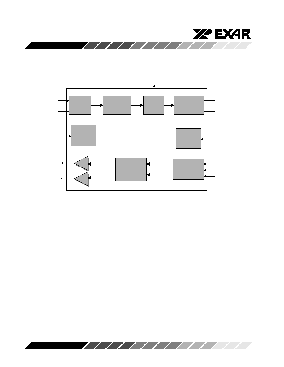
Figure 1. XRT59L91 Block Diagram
Transm it
Input
Interfac
e
Transm it Input
Interface
P ulse
S haping
Circui
t
P ulse S haping
Circuit
Recei
ve
E qualiz
er
Receive
E qualizer
P eak
Detector/
S lice
r
P eak Detector/
S licer
Receive
O utput
Interfac
e
Receive O utput
Interface
LO S
Detect
or
LO S
Detector
Loca
l
Loop
Back
M UX
Local
Loop Back
M UX
Rem ot
e
Loop
Back
M UX
Rem ote
Loop Back
M UX
TTIP
TRing
TxP O S
TxNE G
RTIP
RRing
RLoop
LLoop
R xP O S
R xN E G
RxLO S
TxClk
XRT59L91
3
Rev. P2.00
Preliminary
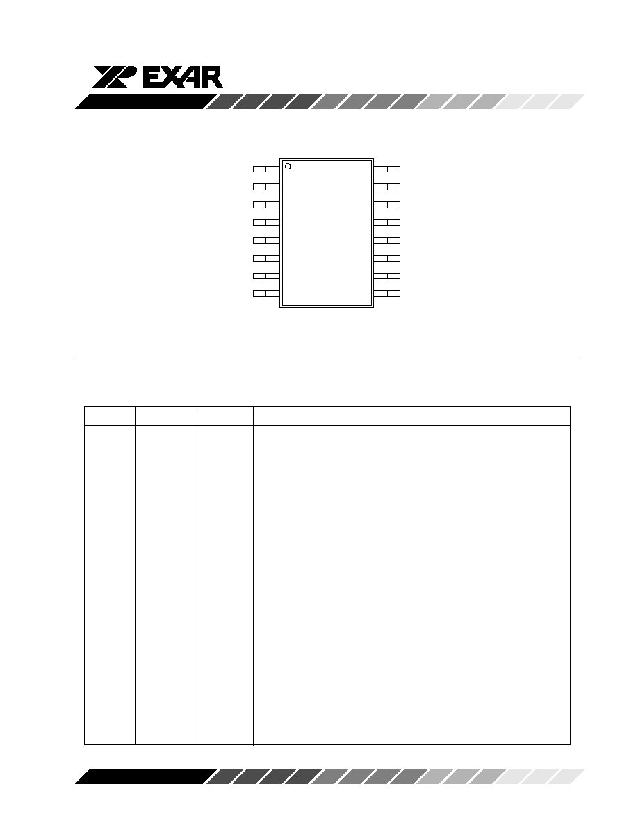
PIN CONFIGURATION
1
9
8
1 6
T x C lk
T x P O S
T V S S
T x N E G
L L oo p
R L o op
R xP O S
R xN E G
R xL O S
T R in g
T V D D
T T IP
R V D D
R V S S
R R ing
R T IP
PIN DESCRIPTION
Pin#
Symbol
Type
Description
1
TxClk
I
Transmitter Clock Input:
If the user operates the LIU in the "clocked" mode, then the "Transmit
Section" of the LIU will use the falling edge of this signal to sample the
data at the TxPOS and TxNEG input pins.
Note: If the user operates the LIU in the "clockless" mode, then the
Terminal Equipment should not apply a clock signal to this input pin.
2
TxPOS
I
Transmit ≠ Positive Data Input:
The exact signal that should be applied to this input pin depends upon
whether the user intends to operate the "Transmit Section" (of the device)
in the "Clocked" or "Clockless" Mode.
Clocked Mode -
The Terminal Equipment should apply bit-wide NRZ pulses on this input
pin, whenever the Terminal Equipment needs to transmit a "positive-
polarity" pulse onto the line via TTIP and TRing output pins. The
XRT59L91 device will sample this input pin upon the falling edge of the
TCLK signal.
Clockless Mode -
The Terminal Equipment should apply RZ pulses to this input pin,
anytime the Terminal Equipment needs to transmit a "positive-polarity"
pulse onto the line via TTIP and TRing output pins.

XRT59L91
4
Rev. P2.00
Preliminary
PIN DESCRIPTION
Pin#
Symbol
Type
Description
3
TxNEG
I
Transmit ≠ Negative Data Input:
The exact signal that should be applied to this input pin depends
upon whether the user intends to operate the "Transmit Section" (of
the device) in the "Clocked" or "Clockless" Mode.
Clocked Mode -
The Terminal Equipment should apply bit-wide NRZ pulses on this
input pin, whenever the Terminal Equipment needs to transmit a
"negative-polarity" pulse onto the line via TTIP and TRing output
pins. The XRT59L91 device will sample this input pin upon the
falling edge of the TClk signal.
Clockless Mode -
The Terminal Equipment should apply RZ pulses to this input pin,
anytime the Terminal Equipment needs to transmit a "negative-
polarity" pulse onto the line via TTIP and TRing output pins.
4
LLoop
I
Local Loopback Input Select:
This input pin permits the user to configure the XRT59L91 device to
operate in the "Local Loopback" Mode; in order to support Diagnostic
Operations.
When the XRT59L91 device is operating in the Local Loopback
Mode, then TTIP and TRing output signals will be (internally)
routed to RTIP and RRing input signals.
Setting this input pin "high" configures the XRT59L91 device to
operate in the "Local Loopback" Mode. Setting this input pin "low"
configures the XRT59L91 device to operate in the "Normal" Mode.
Note: Pulling both the "LLoop" and "RLoop" input pins to VDD,
simultaneously, will cause the XRT59L91 device to operate in the "In-
Circuit Test" Mode. In this mode, all output pins will be tri-stated.
5
RLoop
I
Remote Loopback Input Select:
This input pin permits the user to configure the XRT59L91 device to
operate in the "Remote Loopback" Mode; in order to support Diagnos-
tic Operations.
When the XRT59L91 device is operating in the Remote Loopback
Mode, then the RxPOS and RxNEG output pins will be (internally)
routed to the TxPOS and TxNEG input pins.
Setting this input pin "high" configures the XRT59L91 device to
operate in the "Remote Loopback" Mode. Setting this input pin "low"
configures the XRT59L91 device to operate in the "Normal" Mode.
Note: Pulling both the "LLoop" and "RLoop" input pins to VDD,
simultaneously, will cause the XRT59L91 device to operate in the "In-
Circuit Test" Mode. In this mode, all output pins will be tri-stated.

XRT59L91
5
Rev. P2.00
Preliminary
PIN DESCRIPTION
Pin#
Symbol
Type
Description
6
RxPOS
O
Receive Positive Pulse Output:
This output pin will pulse "high" whenever the XRT59L91 device has
received a "Positive Polarity" pulse, in the incoming line signal, at
RTIP/RRing inputs.
7
RxNEG
O
Receive Negative Pulse Output:
This output pin will pulse "high" whenever the XRT59L91 device has
received a "Negative Polarity" pulse, in the incoming line signal, at
RTIP/RRing inputs.
8
RxLOS
O
Receive Loss of Signal Output Indicator:
This output pin toggles "high" if the XRT59L91 device has detected a
"Loss of Signal" condition in the incoming line signal.
9
RTIP
I
Receive TIP Input:
This input pin, along with RRing is used to receive the bipolar line
signal from the "Remote E1 Terminal".
10
RRing
I
Receive Ring Input:
This input pin, along with RTIP is used to receive the bipolar line
signal from the "Remote E1 Terminal".
11
RVSS
-
Receiver Ground Pin
12
RVDD
-
Receiver Power Supply Pin: 3.3V + 5%
13
TTIP
O
Transmit TIP Output:
The XRT59L91 device will use this pin, along with TRing, to transmit
a bipolar line signal, via a 1:2 step-up transformer.
14
TVDD
-
Transmitter Power Supply Pin: 3.3V + 5%
15
TRing
O
Transmit Ring Output:
The XRT59L91 device will use this pin, along with TTIP, to transmit a
bipolar line signal, via a 1:2 step-up transformer.
16
TVSS
-
Transmitter Ground Pin

XRT59L91
6
Rev. P2.00
Preliminary
AC ELECTRICAL CHARACTERISTICS 25∞C
Unless otherwise specified: T
A
= V
DD
=3.3V±5%, unless otherwise specified.
DC ELECTRICAL CHARACTERISTICS 25∞C
Unless otherwise specified: T
A
=-, V
DD
=3.3V±5%, unless otherwise specified.
Parameter
Symbol
Min
Typ
Max
Unit
Power Supply Voltage
V
DD
3.13
3.3
3.46
V
Input High Voltage
V
IH
2.0
-
5.0
V
Input Low Voltage
V
IL
-0.5
-
0.8
V
Output High Voltage @ I
OH
= -4mA
V
OH
2.4
-
-
V
Output Low Voltage @ I
OL
= 4mA
V
OL
-
-
0.4
V
Input Leakage Current
(except Input pins with pull-up resistor
I
L
-
-
± 10
m
A
Input Capacitance
CI
-
5.0
-
pF
Output Load Capacitance
C
L
-
-
25
pF
Power Consumption including the line power dissipation, tranmission and receive paths all active
Unless otherwise specified: T
A
=-40 to 85∞C, V
DD
=3.3V±5%, unless otherwise specified.
Parameter
Symbol
Min
Typ
Max
Unit
Conditions
Power Consumption
PC
-
130
145
mW
75
W
load, operating at
50% Mark Density
Power Consumption
PC
-
115
130
mW
120
W
load, operating at
50% Mark Density
Power Consumption
PC
-
170
185
mW
75
W
load, operating at
100% Mark Density
Power Consumption
PC
-
140
155
mW
120
W
load, operating at
100% Mark Density
Power Consumption
PC
-
25
30
mW
Transmitter in Powered-
down mode
Parameter
Symbol
Min
Typ
Max
Unit
TClk Clock Period
T1
-
488
-
n s
TClk Duty Cycle
T2
47
50
53
%
Transmit Data Setup Time
TSU
50
-
-
n s
Transmit Data Hold Time
THO
30
-
-
ns
Transmit Data Prop. Delay Time
T3
- RZ data Mode
-
50
-
n s
- NRZ data Mode (clock mode)
-
50
-
n s
TClk Rise Time(10%/90%)
TR
-
-
40
n s
TClk Fall Time(90%/10%)
TF
-
-
40
n s
Receive Data Rise Time
Rtr
-
-
40
n s
Receive Data Fall Time
Rtf
-
-
40
n s
Receive Data Prop. Delay
Rpd
-
160
-
n s
Receive Data Pulse Width
Rxpw
210
244
450
n s
XRT59L91
7
Rev. P2.00
Preliminary
RECEIVER ELECTRICAL CHARACTERISTICS
T
A
=-40 to 85∞C, V
DD
=3.3V±5%, unless otherwise specified.
Parameter
Min
Typ
Max
Unit
Test Conditions
Receiver Loss of Signal:
Threshold to Assert
12
20
-
dB
Cable attenuation @ 1024KHz
Threshold to Clear
11
15
dB
Time Delay
10
-
255
bit
per ITU-G.775
Hysteresis
-
5
-
dB
Receiver Sensitivity
11
13
-
dB
Below nominal pulse amplitude of 3.0V
for 120
W
and 2.37V for 75
W
applications.
With -18dB interference signal added.
Interference Margin
-18
-14
-
dB
With 6dB cable loss
Input Impedance
-
5
-
K
W
Jitter Tolerance:
20Hz
10
700Hz
5
-
-
UIpp
10KHz --100KHz
0.3
Return Loss:
51KHz --102KHz
14
-
-
dB
102KHz--2048KHz
20
-
-
dB
per ITU-G.703
2048KHz--3072KHz
16
-
-
dB
TRANSMITTER ELECTRICAL CHARACTERISTICS
T
A
=-40 to 85∞C, V
DD
=3.3V±5%, unless otherwise specified.
Parameter
Min
Typ
Max
Unit
Test Conditions
AMI Output Pulse Amplitude:
75
W
Application
2.13
2.37
2.60
V
Use transformer with 1:2 ratio
120
W
Application
2.70
3.00
3.30
and 9.1
W
resistor in series
with each end of primary.
Output Pulse Width
224
244
264
ns
Output Pulse Width Ratio
0.95
1.00
1.05
-
per ITU-G.703
Output Pulse Amplitude Ratio
0.95
1.00
1.05
-
per ITU-G.703
Output Return Loss:
51KHz --102KHz
10
-
-
dB
102KHz--2048KHz
16
-
-
dB
per ETSI 300 166 and CH PTT
2048KHz--3072KHz
12
-
-
dB
ABSOLUTE MAXIMUM RATINGS
Storage Temperature
-65∞C to + 150∞C
Operating Temperature
-40∞C to + 85∞C
Supply Voltage
-0.5V to + 6.0V

XRT59L91
8
Rev. P2.00
Preliminary
SYSTEM DESCRIPTION
The XRT59L91 device is a single channel E1 trans-
ceiver that provides an electrical interface for
2.048Mbps applications. XRT59L91 includes a receive
circuit that converts an ITU-T G.703 compliant bipolar
signal into a TTL compatible logic levels. Each receiver
also includes an LOS (Loss of Signal) detection circuit.
Similarly, in the Transmit Direction, the Transmitter
converts TTL compatible logic levels into a G.703
compatible bipolar signal. The Transmitter may be
operated in either a "Clocked" or "Clockless" Mode.
The XRT59L91 device consists of both a Transmit
Section and a Receive Section; each of these sections
will be discussed in detail below.
1.0
The Transmit Section
In general, the purpose of the "Transmit Section"
(within the XRT59L91 device) is to accept TTL/CMOS
level digital data (from the Terminal Equipment), and to
encode it into a format such that it can:
1. Be efficiently transmitted over coaxial- or twisted-
pair cable at the E1 data rate; and
2. Be reliably received by the Remote Terminal
Equipment at the other end of the E1 data link.
3. Comply with the ITU-T G.703 pulse template
requirements, for E1 applications.
The circuitry that the Transmit Section (within the
XRT59L91 device) uses to accomplish this goal is
discussed below. The Transmit Section of the
XRT59L91 device consists of the following blocks:
l
Transmit Input Interface
l
Pulse Shaping Block
1.1
The Transmit Input Interface
The Transmit Input Interface accepts either "clocked" or
"clockless" data from the Terminal Equipment. The
manner in which the Terminal Equipment should apply
data to the XRT59L91 device depends upon whether the
device is being operated in the "clocked" or "clockless"
mode.
1.2.1 Operating the Transmitter in the Clocked
Mode
The user can configure the XRT59L91 device to operate
in the "Clocked" mode by simply applying a 2.048MHz
clock signal to the "TxClk" input pin. The XRT59L91
device contains detectioncircuitry that sense activity on
the "TxClk" line. If this circuit senses activity on the
"TxClk" line, then the XRT59L91 will automatically be
operating in the "Clocked" Mode.
In the Clocked Mode, a 2.048 mHz clock should be
applied toTxClk input pin and NRZ data at the TxPOS
and TxNEG input pins. The "Transmit Input Interface"
circuit will sample the data, at the TxPOS and TxNEG
input pins, upon the falling edge of TxClk, as illustrated
below.

XRT59L91
9
Rev. P2.00
Preliminary
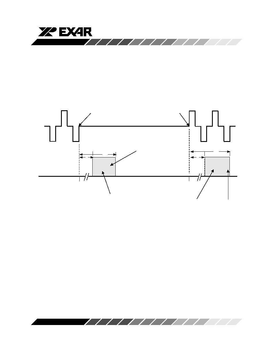
TClk
TxP O S
TxNE G
tS U
tHO
Figure 2. Illustration on how the XRT59L91 Device Samples the data on the
TXPOS and TXNEG input pins
In general, if the XRT59L91 device samples a "1" on the
TxPOS input pin, then the "Transmit Section" of the
device will ultimately generate a positive polarity pulse
via the TTIP and TRing output pins (across a 1:2
transformer). Conversely, if the XRT59L91 device
samples a "1" on the "TxNEG" input pin, then the
"Transmit Section" of the device will ultimately generate
a negative polarity pulse via the TTIP and TRing output
pins (across a 1:2 transformer).
1.2.1 Operating the Transmitter in the
"Clockless" Mode
The user can configure the XRT59L91 device to oper-
ate in the "Clockless" mode by doing the following:
l
Not applying a clock signal to the TXClk input,
and either pulling this pin to VDD or letting it float.
l
By applying RZ (Return to Zero) data to the
TxPOS and TxNEG input pins, as illustrated
below.
T xP O S
T xN E G
T xC lk
D a ta 1 1 0 1 1 0 1
B it
P e rio d
R Z P u lse w id th
sh o u ld co n fo rm to
G .7 0 3 T e m p la te
N o p u lse is to b e a p p lie d
in th e se co n d h a lf o f th e
b it p e rio d
N o A ctivity in
T xC lk L in e
Figure 3. IIlustration on how the Terminal Equipment should apply data to the "Transmit Sec-
tion" of the XRT59L91 Device, when operating in the "Clockless" Mode

XRT59L91
10
Rev. P2.00
Preliminary
Figure 3, indicates that when the user is operating the
XRT59L91 device in the "Clockless" Mode, then the
Terminal Equipment must do the following.
l
Not apply a signal on the "TxClk" line.
l
When applying a pulse (to either the TxPOS or
TxNEG input pin), apply an RZ pulse to the
appropriate input pin. This RZ pulse should only
have a width of one-half the bit-period. Addition,
the RZ pulse should occupy only the first half of
the bit-period. The TxPOS and TxNEG input pins
must be at 0V, during the second half of every bit-
period.
1.3
The Pulse Shaping Circuit
The purpose of the "Transmit Pulse Shaping" circuit is
to generate "Transmit Output" pulses that comply with
the ITU-T G.703 Pulse Template Requirements for E1
Applications.
An illustration of the "ITU-T G.703 Pulse Template
Requirements" is presented below in Figure 4.
0%
50%
V = 100%
244ns
Nominal Pulse
219ns
(244 - 25)
269ns
(244 + 25)
194ns
10%
10%
20%
Figure 4. Illustration of the ITU-T G.703 Pulse Template for E1 Application

XRT59L91
11
Rev. P2.00
Preliminary
With input signal as described above, the XRT59L91
device will take each mark (which is provided to it via the
"Transmit Input Interface" block, and will generate a
pulse that complies with the pulse template, presented
in Figure 4 (when measured on the secondary-side of
the Transmit Output Transformer).
1.2
Interfacing the Transmit Section of the
XRT59L91 device to the Line
ITU-T G.703 specifies that the E1 line signal can be
transmitted over coaxial cable and terminated with 75
W
or transmitted over twisted-pair and terminated with
120
W
.
In both applications (e.g., 75
W
or 120
W
), the user is
advised to interface the Transmitter to the Line, in the
manner as depicted in Figures 5 and 6, respectively.
Figure 5. Illustration of how to interface the Transmit Section of the
XRT59L91 device to the Line (for "75
W
W
W
W
W
" Applications)
U
1
XR T59L91
T T IP
1
3
T R in g
1
5
T xP O S
2
T xN E G
3
T xC lk
1
R
1
9 .
1
1
2
R
2
9 .
1
1
2
1 :
2
P E -
6 5 8 3 5
1
5
4
8
J
1
B N
C
1
2
T xP O S
T xN E G
T xL in e C lk

XRT59L91
12
Rev. P2.00
Preliminary
U 1
X R T 59 L 9 1
T T IP
1 3
T R ing
1 5
T xP O S
2
T xN E G
3
T xC lk
1
1 :2
P E -65 8 35
1
5
4
8
R 1
9 .1
1
2
R 2
9 .1
1
2
T T IP
T R IN G
T xP O S
T xN E G
T xL in eC lk
Figure 6. Illustration of how to interface the Transmit Section of the XRT59L91
device to the Line (for "120
W
W
W
W
W
" Applications)
Notes:
1. Figures 5 and 6 indicate that for both "75
W
and "120
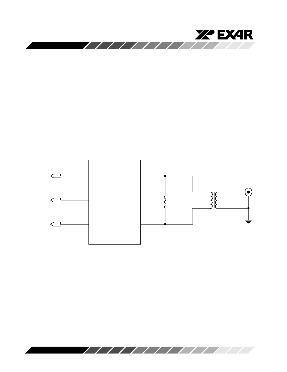
W
"
applications, the user should connect a 9.1
W
resistor,
in series, between the TTIP/TRing outputs and the
transformers.
2. Figure 5 and 6 indicate that the user should a "1:2
STEP-UP" Transformer.
XRT59L91
13
Rev. P2.00
Preliminary
Parameter
Value
Turns Ratio
1:2
Primary Inductance
Isolation Voltage
Leakage Inductance
Transmit Transformer Recommendations
Part Num ber
Vendor
Isolation
Package Type
PE-65835
Pulse
TTI 7154-R
Transpower Technologies, Inc.
TG26-1205
HALO
The Following Transformers Are Recommended For Use:
Note:
More transformers will be added to this list as we take
the time to evaluate these transformers.
Magnetic Supplier Information
Pulse
Corporate Office
12220 World Trade Drive
San Diego, CA 92128
Tel: (619)-674-8100
FAX: (619)-674-8262
Europe
1 & 2 Huxley Road
The Surrey Research Park
Guildford, Surrey GU2 5RE
United Kingdom
Tel: 44-1483-401700
FAX: 44-1483-401701
Asia
150 Kampong Ampat
#07-01/02
KA Centre
Singapore 368324
Tel: 65-287-8998
FAX: 65-280-0080
Transpower Technologies
Corporate Office
9410 Prototype Drive, Ste #1
Reno, NV 89511
Tel: (800)511-7308 or
(775)852-0140
Fax: (775)852-0145
www.trans-power.com
HALO Electronics
HALO Electronics
P.O. Box 5826
Redwood City, CA 94063
Tel: (650)568-5800
FAX: (650)568-6161
XRT59L91
14
Rev. P2.00
Preliminary
2.0 The Receive Section
The Receive Section of the XRT59L91 device consists
of the following blocks:
l
The "Receive Equalizer" block
l
The "Peak Detector" and "Slicer" block
l
The "LOS Detector" block
l
The "Receive Output Interface" block
2.1 Interfacing the Receive Section to the Line
The design of the XRT59L91 device permits the user
to transformer-couple or capacitive-couple the Re-
ceive Section to the line. Additionally, as mentioned
earlier, the specification documents for E1 specify
75
W
termination loads, when transmitting over coaxial
cable, and 120
W
loads, when transmitting over twisted-
pair. Figures 7 through 9 present the various methods
that the user can employ in order to interface the
Receiver (of the XRT59L91 device) to the line.
U 1
X RT5 9L91
R T IP
9
R R in g
1 0
R xP O S
6
R xN E G
7
R xL O S
8
1 :2
P E -6 58 3 5
1
5
4
8
R L
1 8.7
1
2
J1
B N C
1
2
L oss o f S ig na l
R xN E G
R xP O S
Figure 7. Recommended Schematic for Interfacing the Receive Section of the XRT59L91
Device to the Line for 75
W
W
W
W
W
Applications (Transformer-Coupling)

XRT59L91
15
Rev. P2.00
Preliminary
U 1
XRT59L91
R T IP
9
R R in g
1 0
R x P O S
6
R x N E G
7
R x L O S
8
1 :2
P E -6 5 8 3 5
1
5
4
8
R L
3 0 .1
1
2
R T IP
R R IN G
R x P O S
R x N E G
L o s s o f S ig n a l
Figure 8. Recommended Schematic for Interfacing the Receive Section of the XRT59L91
Device to the Line for 120
W
W
W
W
W
Applications (Transformer-Coupling)
Note:
Figures 7 and 8 indicate that the user should use a "2:1
STEP-DOWN" transformer, when interfacing the re
ceiver to the line.
U 1
X RT59L91
R T IP
9
R R in g
1 0
R x P O S
6
R x N E G
7
R x L O S
8
C 1
0 .1 u F
1
2
C 2
0 .1 u F
1
2
R 2
3 7 .4
1
2
R 1
3 7 .4
1
2
R T IP
R R IN G
R x P O S
R x N E G
L o ss o f S ig n a l
Figure 9. Recommended Schematic for Interfacing the Receive Section of the XRT59L91
Device to the Line for 75
W
W
W
W
W
Applications (Capacitive-Coupling)

XRT59L91
16
Rev. P2.00
Preliminary
2.2
The "Receive Equalizer" Block
After the XRT59L91 device has received the incoming
line signal, via the RTIP and RRing input pins, the first
block that this signal will pass through is the Receive
Equalizer block.
As the line signal is transmitted from a given "Transmit-
ting" terminal, the pulse shapes (at that location) are
basically "square". As this line signal travels from the
"transmitting terminal" (via the coaxial cable or twisted
pair) to the receiving terminal, it will be subjected to
"frequency-dependent" loss. In other words, the higher
frequency components of the signal will be subjected
to a greater amount of attenuation than will the lower
frequency components. If this line signal travels over
reasonably long cable lengths, then the shape of the
pulses (which were originally square) will be distorted
and cause inter-symbol interference to increase.
The purpose of this block is to equalize the incoming
distorted signal, due to cable loss. In essence, the
Receive Equalizer block accomplishes this by subject-
ing the received line signal to "frequency-dependent"
amplification (which attempts to counter the fre-
quency-dependent loss that the line signal has experi-
enced). By doing this, the Receive Equalizer is
attempting to restore the shape of the line signal so that
the received data can be recovered reliably.
2.3
The "Peak Detector and Slicer Block
After the incoming line signal has passed through the
Receive Equalizer block, it will be routed to the "Slicer"
block. The purpose of the "Slicer" block is to quantify
a given bit-period (or symbol) within the incoming line
signal as either a "1" or a "0".
2.4
The "LOS Detector" Block
The LOS Detector block, within the XRT59L91 was
specifically designed to comply with the "LOS Decla-
ration/Clearance" requirements per ITU-T G.775. As a
consequence, the XRT59L91 device will declare an
LOS Condition, (by driving the "RxLOS" output pin
"high") if the received line signal amplitude drops to ≠
35dB or below. Further, the XRT59L91 device will clear
the LOS Condition if the signal amplitude rises back up
to ≠12dB or above. Figure 10 presents an illustration of
G.775 spec for declaring and clearing LOS.
0 dB
-6 dB
-9dB
-35dB
Maximum Cable Loss for E1
LOS Signal Must be Declared
LOS Signal Must be Cleared
LOS Signal may be Cleared or Declared
Figure 10. Illustration of G.775 Spec.
XRT59L91
17
Rev. P2.00
Preliminary
Timing Requirements associated with Declaring
and Clearing the LOS Indicator.
The XRT59L91 device was designed to meet the ITU-
T G.775 specification timing requirements for declar-
ing and clearing the LOS indicator. In particular, the
XRT59L91 device will declare LOS, between 10 and 255
UI (or E1 bit-periods) after the actual time the LOS
condition occurred. Further, the XRT59L91 device will
A ctu a l
O ccu rre n ce
o f L O S
C o n d itio n
L in e
S ig n a l
is
R e sto re d
T im e R a n g e
fo r
L O S
D e cla ra tio n
T im e R a n g e
fo r
L O S
C le a ran ce
G .7 7 5 C o m p lia n ce
G .7 7 5 C o m p lia n ce
0
U I
10 U I
0
U I
10 U I
255 U I
255 U I
R X IN
L O S O u tp u t P in
N o te : F o r E 1 , 1 U I = 4 8 8 n s
clear the LOS indicator within 10 to 255 UI after
restoration of the incoming line signal. Figure 11
illustrates the LOS Declaration and Clearance behav-
ior, in response to first, the "Loss of Signal" event and
then afterwards, the restoration of the signal.
Figure 11. The Behavior of the LOS Output Indicator, in response to the Loss of Signal,
and the Restoration of the Signal
2.5
The "Receive Output Interface" Block
The purpose of the "Receive Output Interface" block is
to interface directly with the "Receiving Terminal
Equipment". The "Receive Output Interface" block
outputs the data (which has been recovered from the
incoming line signal) to the "Receive Terminal Equip-
ment" via the "RxPOS and RxNEG output pins.
If the "Receive Section" of the XRT59L91 device has
received a "Positive-Polarity" pulse, via the RTIP and
RRing input pins, then the Receive Output Interface will
output a pulse at the "RxPOS" output pin.
Similarly, if the "Receive Section" of the XRT59L91
device has received a "Negative-Polarity" pulse, via
the RTIP and RRing input pins, then the Receive Output
Interface will output a pulse at the "RxNEG" output pin.
XRT59L91
18
Rev. P2.00
Preliminary
3.0
Diagnostic Features
In order to support diagnostic operations, the
XRT59L91 supports the following loopback modes:
l
Local Loopback
l
Remote Loopback
Each of these loopback modes will be discussed
below.
3.1
The Local Loop-Back Mode
When the XRT59L91 device is configured to operate in
the "Local Loop-back" Mode, the XRT59L91 device will
ignore any signals that are input to the RTIP and RRing
input pins. The "Transmitting Terminal Equipment" will
transmit data (and clock, for "Clocked"
Mode) into the XRT59L91 device via the TxPOS,
TxNEG and TxCLK input pins. This data will be
processed through the "Transmit Terminal Input Inter-
face" and the "Pulse Shaping" circuit. Finally, this data
will be output to the line via the TTIP and TRing output
pins. Additionally, this data (which is being output via
the TTIP and TRing output pins) will be looped back into
the "Receive Equalizer" block. As a consequence, this
data will also be processed through the entire "Receive
Section" of the XRT59L91 device. After this "post-loop-
back" data has been processed through the "Receive
Section" it will output, to the "Near-End Receiving
Terminal Equipment" via the "RxPOS and RxNEG
output pins.
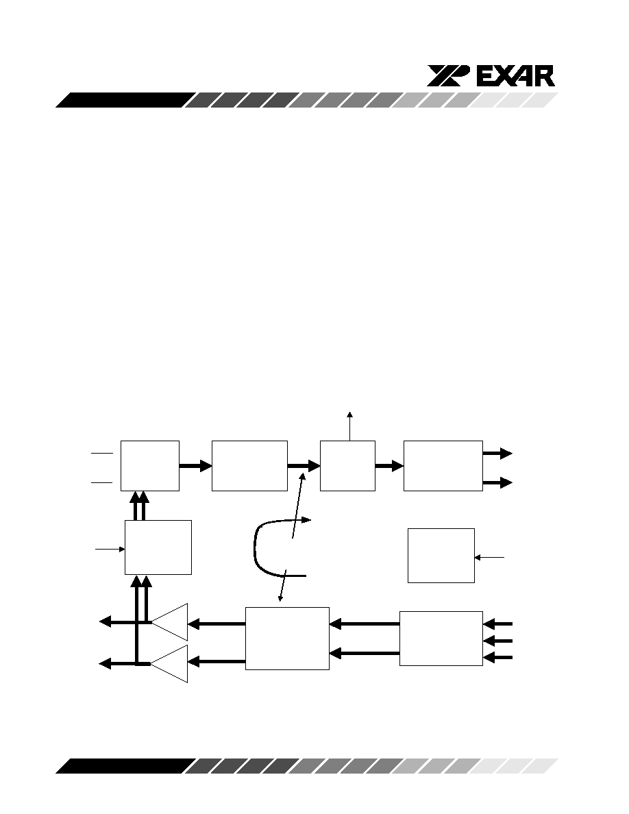
Figure 12, illustrates the path that the data takes
(within the XRT59L91 device), when the chip is config-
ured to operate in the "Local Loop-back" Mode.
Local Loop B ack
P ath
T ra nsm it Input
Interface
P ulse S haping
C ircu it
R ece ive
E qua lizer
P eak D etector/
S licer
R ece ive O utput
Interface
LO S
D etector
Local
Loop B ack
M U X
R em ote
Loop B ack
M U X
T T IP
T R ing
T xP O S
T xN E G
R T IP
R R ing
R Loop
LLoop
R xP O S
R xN E G
R xLO S
T xC lk
Figure 12. Illustration of the "Local Loop-back" within the XRT59L91 Device
XRT59L91
19
Rev. P2.00
Preliminary
The user can configure the XRT59L91 device to oper-
ate in the "Local Loop-back" Mode, by pulling the
"LLoop" input pin (pin 4) to VDD.
3.2
The Remote Loop Back Mode
When the XRT59L91 device is configured to operate in
the "Remote Loop-back" Mode, the XRT59L91 device
will ignore any signals that are input to the TxPOS and
TxNEG input pins. The XRT59L91 device will receive
the incoming line signals, via the RTIP and RRing input
pins. This data will be processed through the entire
Receive Section (within the XRT59L91) and will output
to the "Receive Terminal Equipment" via the
R em o te Loop B a ck
P a th
T ransm it In put
In terface
T ransm it In put
In terface
P u lse S ha ping
C ircuit
P u lse S ha ping
C ircuit
R eceive
E q ualize r
R eceive
E q ualize r
P e ak D ete ctor/
S licer
P e ak D ete ctor/
S licer
R eceive O utpu t
In terface
R eceive O utpu t
In terface
LO S
D etector
LO S
D etector
Lo cal
Lo op B ack
M U X
Lo cal
Lo op B ack
M U X
R em o te
Lo op B ack
M U X
R em o te
Lo op B ack
M U X
T T IP
T R ing
T xP O S
T xN E G
R T IP
R R ing
R Loop
LL oop
R xP O S
R xN E G
R xLO S
T xC lk
"RxPOS" and "RxNEG" output pins. Additionally, this
data will also be internally looped back to the "Transmit
Input Interface" block within the "Transmit Section". At
this point, this data will be routed through the remainder
of the "Transmit Section" of the XRT59L91 device and
will be transmitted out onto the line via the "TTIP" and
"TRing" output pins.
Figure 13, illustrates the path that the data takes
(within the XRT59L91 device) when the chip is config-
ured to operate in the "Remote Loop-back" Mode.
Figure 13. Illustration of the "Remote Loop-back" path, within the XRT59L91 Device
It should be noted that during "Remote Loop-back"
operation, any data which is input via the RTIP and
RRING input pins, will also be output to the Terminal
Equipment, via the RxPOS and RxNEG output pins.
XRT59L91
20
Rev. P2.00
Preliminary
4.0 Shutting off the Transmitter
The XRT59L91 device permits the user to shut the
"Transmit Driver" within the Transmit Section of the
chip. This feature can be useful for system redundancy
design considerations or during diagnostic testing.
The user can activate this feature by either of the
following ways.
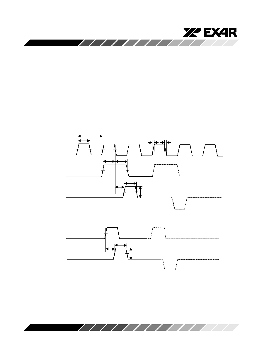
T C lk
T xP O S o r
T N E G
T T IP /
T R in g
T
H O
T
S U
T3
T
R
T
F
T xP O S o r
T N E G
T T IP /
T R in g
N RZ M ode (C lock M ode)
R Z M ode (None-C lock M ode)
T3
T
X P W
T X O U T
V
T X O U T
V
T
X P W
T
2
T
1
Method 1:
Connect the Transmit Data input pins (e.g., TxPOS
and TxNEG) to a logic "1"; or allow them to float.
(These input pins have an internal "pull-up" resistor).
Method 2:
Connect the "TxClk" input pin to a logic "0" (e.g., GND)
and continue to apply data via the TxPOS and TxNEG
input pins.
Figure 14. Transmit Timing Diagram

XRT59L91
21
Rev. P2.00
Preliminary
R T IP /
R R in g
R x P O S
R x p w
R p d
R x N E G
R tr
R tf
Figure 15. Receive Timing Diagram
APPLICATIONS INFORMATION
Figures 16, 17 and 18, provide example schematics on
how to interface the XRT59L91 device to the line, under
the following conditions:
l
Receiver is Transformer-coupled to a 75
W
unbalanced line.
l
Receiver is Transformer-coupled to a 120
W
balanced line.
l
Receiver is Capacitive-coupled to a 75
W
unbalanced line

XRT59L91
22
Rev. P2.00
Preliminary
U 1
XRT59L91
T xP O S
2
T xN E G
3
T xC lk
1
R xP O S
6
R xN E G
7
R xL O S
8
R R in g
1 0
R TIP
9
T R in g
1 5
T TIP
1 3
R 1
9 .1
1
2
R 2
9 .1
1
2
1 :2
P E -6 5 83 5
1
5
4
8
J1
B N C
1
2
R 3
1 8.7
1
2
1 :2
P E -6 5 83 5
1
5
4
8
J2
B N C
1
2
T xP O S
T xN E G
T xLin eC lk
R xP O S
R xN E G
L oss o f S ig n a l
Figure 16. Illustration on how to interface the XRT59L91 Device to the Line
(Receiver is Transformer-coupled to a 75
W
W
W
W
W
unbalanced line)

XRT59L91
23
Rev. P2.00
Preliminary
U 1
X R T59L 91
T x P O S
2
T x N E G
3
T x C lk
1
R x P O S
6
R x N E G
7
R x LO S
8
R R in g
1 0
R T IP
9
T R in g
1 5
T T IP
1 3
1 :2
P E -6 5 83 5
1
5
4
8
1 :2
P E -6 5 83 5
1
5
4
8
R 1
9 .1
1
2
R 2
9 .1
1
2
R 3
3 0.1
1
2
L os s of S ign a l
R x N E G
R x P O S
T x P O S
T x N E G
T x LIn e C lk
T T IP
T R IN G
R T IP
R R IN G
Figure 17. Illustration on how to interface the XRT59L91 Device to the Line
(Receiver is Transformer-coupled to a 120
W
W
W
W
W
balanced line)

XRT59L91
24
Rev. P2.00
Preliminary
U 1
X R T 59L 91
T xP O S
2
T xN E G
3
T xC lk
1
R xP O S
6
R xN E G
7
R xL O S
8
R R ing
1 0
R T IP
9
T R ing
1 5
T T IP
1 3
R 4
3 7 .4
1
2
R 1
9 .1
1
2
R 2
9 .1
1
2
C 1
0 .1 u F
1
2
C 2
0 .1 u F
1
2
R 3
3 7 .4
1
2
1 :2
P E -6 5 83 5
1
5
4
8
J1
B N C
1
2
J2
B N C
1
2
T xP O S
T xN E G
T xL in e C lk
R xP O S
R xN E G
L o ss o f S ig n al
Figure 18. Illustration on how to interface the XRT59L91 Device to the Line
(Receiver is Capacitive-coupled to a 75
W
W
W
W
W
unbalanced line)

XRT59L91
25
Rev. P2.00
Preliminary

XRT59L91
26
Rev. P2.00
Preliminary
Notes

XRT59L91
27
Rev. P2.00
Preliminary
Notes

XRT59L91
28
Rev. P2.00
Preliminary
NOTICE
EXAR Corporation reserves the right to make changes to the products contained in this publication in order to improve
design, performance or reliability. EXAR Corporation assumes no responsibility for the use of any circuits described
herein, conveys no license under any patent or other right, and makes no representation that the circuits are free of
patent infringement. Charts and schedules contained here in are only for illustration purposes and may vary depending
upon a user's specific application. While the information in this publication has been carefully checked; no
responsibility, however, is assumed for in accuracies.
EXAR Corporation does not recommend the use of any of its products in life support applications where the failure
or malfunction of the product can reasonably be expected to cause failure of the life support system or to significantly
affect its safety or effectiveness. Products are not authorized for use in such applications unless EXAR Corporation
receives, in writing, assurances to its satisfaction that: (a) the risk of injury or damage has been minimized; (b) the
user assumes all such risks; (c) potential liability of EXAR Corporation is adequately protected under the
circumstances.
Copyright 1999 EXAR Corporation
Datasheet October 1999
Reproduction, in part or whole, without the prior written consent of EXAR Corporation is prohibited.