 | –≠–ª–µ–∫—Ç—Ä–æ–Ω–Ω—ã–π –∫–æ–º–ø–æ–Ω–µ–Ω—Ç: XRT6164CP | –°–∫–∞—á–∞—Ç—å:  PDF PDF  ZIP ZIP |
EXAR Corporation, 48720 Kato Road, Fremont, CA 94538
∑
(510) 668-7000
∑
FAX (510) 668-7017
Rev. 3.0.0
XRT6164
Digital Line Interface Transceiver
September 2003
FEATURES
l
Single 5V Supply
l
CCITT G.703 Compatible When Used With
Either XR-T6165 or XR-T6166
l
Low Power
l
TTL Compatible Digital Inputs and Outputs
l
Links Remote Equipment at Distances up to
500 Meters Without Equalization
l
Receive Data Comparator Threshold Storage
Provides Ping-Pong Operation Capability
l
Loss of Signal Alarm
l
Dual Matched Driver Outputs
ORDERING INFORMATION
Operating
Part No.
Package
Temperature Range
XRT6164CP
16-Lead 300 Mil PDIP
0∞C to +70∞C
XRT6164CD
16-Lead 300 Mil JEDEC SOIC
0∞C to +70∞C
APPLICATIONS
l
Data Adaption Unit (DAU)
l
General Purpose TTL Compatible Line Inter-
face
GENERAL DESCRIPTION
The XRT6164 is a bipolar analog chip intended for general purpose line interface applications at bit rates up to
1.544Mbps (T1). It contains both receive and transmit circuitry in a 16-pin dual-in-line plastic package. The receiver
is designed for short line applications having a cable loss up to 10dB measured at the half bit rate. The transmitter
has open collector line driver outputs that are capable of handling up to 40mA. When used in conjunction with either
XRT6165 or XRT6166, the chip set provides a 64Kbps codirectional interface as specified in CCITT G.703.

XRT6164
2
Rev. 3.0.0
Block DIagram
PEAK CAP
RX+I/P
RX-I/P
TCM CON
V
CC
A
GNDA
TX+I/P
TX-I/P
V
CC
D
GNDD
14
16
1
15
11
6
9
7
Peak
Detector
S + R
12
S - R
RX ALARM
TCM
Control
TX + O/P
10
TX - O/P
8
I/P BIAS
TTL
Buffer
Positive
Data
Comparator
Negative
Data
Comparator
TTL
Buffer
TTL
Buffer
5
3
13
4
Bias
2
Open
Collector
Driver
Open
Collector
Driver
Threshold
Generator
Figure 1. XRT6164 Block Diagram
XRT6164
3
Rev. 3.0.0
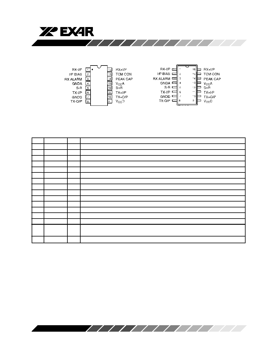
PIN CONFIGURATION
16 Lead PDIP (0.300")
16 Lead SOIC (Jedec, 0.300")
PIN DESCRIPTION
Pin#
Symbol
Type
Description
1
RX-I/P
I
Receiver Negative Bipolar Input. Line analog input.
2
I/P BIAS
O
Receive Input Bias. Connects to center tap of input transformer secondary winding.
3
RX ALARM
O
Loss of Signal Alarm. Active low.
4
GNDA
Analog Ground.
5
S-R
O
Receive Negative Data Output. Output from negative bipolar input pulses (active low).
6
TX-I/P
I
Transmit Negative Input Data. Input for negative output driver (active high).
7
GNDD
Digital Ground.
8
TX-O/P
O
Transmit Negative Output Driver. Open collector, drives output transformer primary.
9
V
CC
D
+5V
+/-5% Digital Supply.
10
TX+O/P
O
Transmit Positive Output Driver. Open collector, drives output transformer primary.
11
TX+I/P
I
Transmit Positive Input Data. Input for positive output driver (active high).
12
S+R
O
Receive Positive Data Output. Output from positive bipolar input pulses (active low).
13
V
CC
A
+5V +/-5% Analog Supply.
14
PEAKCAP
Peak Detector Capacitor. Stores peak detector voltage.
15
TCM CON
I
Time Compression Multiplex Control. When active, disconnects peak detector charge
and discharge paths (active low).
16
RX+I/P
I
Receiver Positive Bipolar Input. Line analog input.

XRT6164
4
Rev. 3.0.0
ELECTRICAL CHARACTERISTICS
Test Conditions: V
CC
= 5V +/- 5%, T
A
= 25∞C, Unless Otherwise Specified
Parameters
Min.
Typ.
Max. Units
Conditions
DC Electrical Characteristics
Supply Voltage
4.75
5
5.25
V
Analog Supply Current
4
8
mA
Digital Supply Current
13
20
mA
Receiver
Input Signal
1
2.2
Vp
Measured from Pins 1 or 16 with Respect to Pin 2
Dynamic Range
10
dB
Maximum Cable Loss Range
Input Impedance
20
k
Measured Between Pins 1 and 16
Input Slicing Threshold
50
%
Percent of Peak Input Signal Amplitude
Input Bias Voltage
1.45
V
Measured at Pin 2
Loss of Signal Alarm Threshold
150
mVp
Measured from Pins 1 or 16 with Respect to Pin 2
Loss of Signal Alarm Level
+/-1.5
dB
Difference Between Alarm-on and Alarm-off
Hysteresis
Levels
Peak Detector Leakage
-80
µ
A
Data Output Low
0.4
V
Measured at Pins 5 or 12, I OUT = +1.6mA
Data Output High
3.6
V
Measured at Pins 5 or 12, I OUT = -40
µ
A
Alarm Output Low
0.4
V
Measured at Pin 3; I OUT = +1.6mA
Alarm Output High
V
CC
-
V
Measured at Pin 3; I OUT = -40
µ
A
0.5
TCM Input Low Voltage
0.8
V
Measured at Pin 15; I IN Min = -500
µ
A, I IN Max =
+5
µ
A
Transmitter
Input Low Voltage
0.8
V
Measured at Pins 6, 11; I IN = -700
µ
A
Input High Voltage
2.2
V
Measured at Pins 6, 11; I IN = +5
µ
A
Output Low Voltage
1
V
Measured at Pins 8, 10; I OUT = -40mA
Output Low Current
40
mA
Measured at Pins 8, 10; V OUT = 1V
Output Leakage Current
-100
µ
A
Measured at Pins 8, 10; V OUT = 10V Outputs in
off state
AC Electrical Characteristics
Receiver
Input Level
1
2.2
Vp
Pin 1, 16 with Respect to Pin 2 1
Output Rise Time
50
ns
Pins 5, 12; C L = 15pF, 10% to 90%
Output Fall Time
50
ns
Pins 5, 12; C L =15pF, 90% to 10%
Notes:
1. Higher input voltages are possible if a resistive input attenuator is used.
Bold face parameters are covered by production test and guaranteed over operating temperature range.

XRT6164
5
Rev. 3.0.0
ELECTRICAL CHARACTERISTIC (CONT'D)
Parameters
Min. Typ. Max. Units Conditions
AC Electrical Characteristics (Cont'd)
Transmitter
Output Rise Time
50
ns
Pins 8, 10; R L = 130, C L = 15pF, 10% to 90%
Output Fall Time
50
ns
Pins 8, 10; R L = 130, C L = 15pF, 90% to 10%
Rising Edge Delay
100
ns
Pins 8, 10; R L = 130, C L = 15pF, 50% to 50%
(I/P to O/P)
Falling Edge Delay
100
ns
Pins 8, 10; R L = 130, C L = 15pF, 50% to 50%
(I/P to O/P)
Notes:
Bold face parameters are covered by production test and guaranteed over operating temperature range.
Specifications are subject to change without notice
ABSOLUTE MAXIMUM RATINGS
Supply Voltage 20V . . . . . . . . . . . . . . . . . . . . . . . . . . . . . . Storage Temperature -65
∞
C to +150
∞
C . . . . . . .
. . . . .
Magnetic Supplier Information:
Pulse
Telecom Product Group
P.O. Box 12235
San Diego, CA 92112
Tel. (619) 674-8100
Fax. (619) 674-8262
Transpower Technologies, Inc.
24 Highway 28, Suite 202
Crystal Bay, NV 89402≠0187
Tel. (702) 831≠0140
Fax. (702) 831≠3521

XRT6164
6
Rev. 3.0.0
SYSTEM DESCRIPTION
The XRT6164 is a general purpose line interface chip
that contains the receive and transmit circuitry neces-
sary to convert TTL logic levels to a bipolar signal both
to and from a twisted pair cable.
Receiver
The XRT6164 receiver section converts a balanced
bipolar signal that has been attenuated and distorted
by up to 10dB of twisted pair cable to active-low TTL
compatible logic levels.
The cable is transformer coupled to the receiver differ-
ential inputs (RX+IP, RX-IP) which are biased through
the input transformer secondary winding by a voltage
generated on-chip (I/P BIAS). The bipolar receive
signal is applied to a peak detector, and to a pair of data
comparators. The peak detector output voltage
charges an external capacitor connected to PEAK
CAP. This voltage generates a data comparator bias
level that is approximately 50% of the peak input pulse
amplitude. Thus, data slicing is automatically accom-
plished at the optimum level over the full cable loss
range. TTL compatible output stages buffer the re-
ceiver digital outputs (S+R, S-R) and provide active
low signals corresponding to received positive and
negative input pulses.
Loss of input signal is detected by a comparator that
monitors input signal level. An active-low TTL compat-
ible logic level (RX ALARM) indicates signal loss.
Comparator hysteresis prevents chatter on this output.
Ping-pong operation is made possible by the time
compression multiplex control input (TCM CON). A
logic 0 applied to this pin during transmission stores the
peak detector output voltage by disconnecting the
peak detector storage capacitor charge and discharge
paths. Since the receive data comparator bias voltage
is stored during transmit mode, it is immediately
available when receive mode resumes.
Transmitter
The XRT6164 transmitter section contains two
matched open collector output drivers that are capable
of driving the line transformer directly with a current up
to 40mA. The transmitter output drivers include diode
clamps to ensure non-saturating operation. Transmit-
ter digital inputs, which are active-high, are TTL com-
patible. External resistors are used between the trans-
mitter outputs and the output transformer primary to set
the output pulse amplitude.
APPLICATION INFORMATION
Figure 2 shows a general line driver application circuit
using the XRT6164. This device converts bipolar
transmit and receive signals in the 64Kbps to
1.544Mbps range to active-low TTL compatible logic
levels.
Bipolar signals that have been attenuated and dis-
torted by twisted pair cable are transformer-coupled to
the line side of the XRT6164 as shown on the left side
of Figure 2. Suggested transformers for both the input
and output applications are the Pulse types PE-65535
or TTI≠7147 for 64Kbps use and the PE-65835 for
1.544Mbps applications.
The right side of Figure 2 shows the TTL compatible
digital inputs and outputs. Please refer to the pin
description section of this data sheet for detailed
information about each signal.

XRT6164
7
Rev. 3.0.0
Figure 2. XRT6164 Line Driver Application
XRT6164

XRT6164
8
Rev. 3.0.0
16 LEAD PLASTIC DUAL-IN-LINE
(300 MIL PDIP)
Rev. 1.00
INCHES
MILLIMETERS
SYMBOL
MIN
MAX
MIN
MAX
A
0.145
0.210 3.68
5.33
A1
0.015
0.070 0.38
1.78
A 2
0.115
0.195 2.92
4.95
B
0.014
0.024 0.36
0.56
B 1
0.030
0.070 0.76
1.78
C
0.008
0.014 0.20
0.38
D
0.745
0.840 18.92
21.34
E
0.300
0.325 7.62
8.26
E 1
0.240
0.280 6.10
7.11
e
0.100 BSC
2.54 BSC
e A
0.300 BSC
7.62 BSC
e B
0.310
0.430 7.87
10.92
L
0.115
0.160 2.92
4.06
0∞
15∞
0∞
15∞
Note: The control dimension is the inch column

XRT6164
9
Rev. 3.0.0
16 LEAD SMALL OUTLINE
(300 MIL JEDEC SOIC)
Rev. 1.00
INCHES
MILLIMETERS
SYMBOL
MIN
MAX
MIN
MAX
A
0.093
0.104 2.35
2.65
A 1
0.004
0.012 0.10
0.30
B
0.013
0.020 0.33
0.51
C
0.009
0.013 0.23
0.32
D
0.398
0.413 10.10
10.50
E
0.291
0.299 7.40
7.60
e
0.050 BSC
1.27 BSC
H
0.394
0.419 10.00
10.65
L
0.016
0.050 0.40
1.27
0∞
8∞
0∞
8∞
Note: The control dimension is the millimeter column

XRT6164
10
Rev. 3.0.0
NOTICE
EXAR Corporation reserves the right to make changes to the products contained in this publication in order to
improve design, performance or reliability. EXAR Corporation assumes no responsibility for the use of any
circuits described herein, conveys no license under any patent or other right, and makes no representation that
the circuits are free of patent infringement. Charts and schedules contained here in are only for illustration
purposes and may vary depending upon a user's specific application. While the information in this publication
has been carefully checked; no responsibility, however, is assumed for inaccuracies.
EXAR Corporation does not recommend the use of any of its products in life support applications where the
failure or malfunction of the product can reasonably be expected to cause failure of the life support system or to
significantly affect its safety or effectiveness. Products are not authorized for use in such applications unless
EXAR Corporation receives, in writing, assurances to its satisfaction that: (a) the risk of injury or damage has
been minimized; (b) the user assumes all such risks; (c) potential liability of EXAR Corporation is adequately
protected under the circum-stances.
Copyright 2003 EXAR Corporation
Datasheet September 2003
Reproduction, in part or whole, without the prior written consent of EXAR Corporation is prohibited.