 | –≠–ª–µ–∫—Ç—Ä–æ–Ω–Ω—ã–π –∫–æ–º–ø–æ–Ω–µ–Ω—Ç: XRT6165 | –°–∫–∞—á–∞—Ç—å:  PDF PDF  ZIP ZIP |
XR-T6165
...the analog plus company
TM
Codirectional Digital
Data Processor
Rev. 2.02
E
1990
EXAR Corporation, 48720 Kato Road, Fremont, CA 94538
z
(510) 668-7000
z
(510) 668-7010
1
May 1997≠3
FEATURES
D
Low Power CMOS Technology
D
All Receiver and Transmitter Inputs and Outputs are
TTL Compatible
D
Transmitter Inhibits Bipolar Violation Insertion for
Transmission of Alarm Conditions
D
Alarm Output Indicates Loss of Received Bipolar
Violations
D
Up to 125
µ
s Variance of Data Transfer Timing in
Both Transmit and Receive Paths Allows Operation
in Plesiochronous Networks
D
Both Receiver and Transmitter Perform Byte
Insertion or Deletion in Response to Local Clock
Slips
APPLICATIONS
D
CCITT G.703 Compliant 64kbps Codirectional
Interface
D
Performs the Digital and Analog Functions for a
Complete 64kbps Data Adaption Unit (DAU) When
Used With the XR-T6164
GENERAL DESCRIPTION
The XR-T6165 is a CMOS device which contains the
digital circuitry necessary to interface both directions of a
64kbps data stream to 2.048Mbps transmit and receive
PCM time-slots. The XR-T6165 and the companion
XR-T6164 line interface chip together form a CCITT
G.703 compliant 64kbps codirectional interface.
The XR-T6165 contains separate transmit and receive
sections. The transmitter transforms 8 bit serial data from
a 2.048Mbps time-slot into an encoded 64kbps data
stream. The receiver, which performs the reverse
operation, decodes the 64kbps data, extracts a clock
signal, and then outputs the data to a 2.048Mbps
time-slot. The XR-T6165 provides features which allow
the repetitions and deletions of both received and
transmitted data as clock skews and transients occur.
ORDERING INFORMATION
Part No.
Package
Operating
Temperature Range
XR-T6165CP
22 Lead 400 Mil PDIP
0
∞
C to +70
∞
C
XR-T6165IP
22 Lead 400 Mil PDIP
≠40
∞
C to +85
∞
C
XR-T6165CD
24 Lead 300 Mil JEDEC SOIC
0
∞
C to +70
∞
C
XR-T6165ID
24 Lead 300 Mil JEDEC SOIC
≠40
∞
C to +85
∞
C
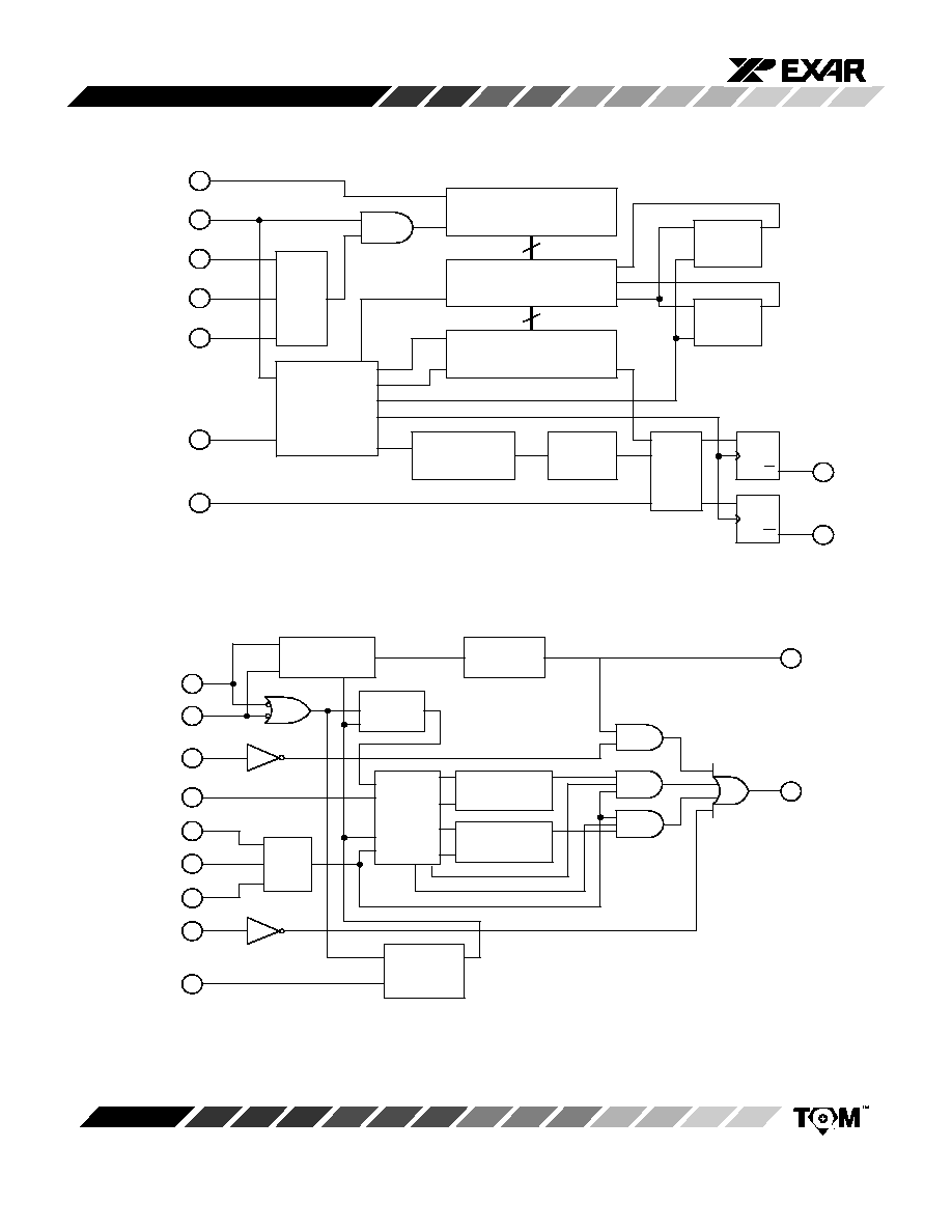
XR-T6165
2
Rev. 2.02
21
22
RXCK2MHz
18
ALARMIN
TX256kHz
PCMIN
Byte
Deletion
8 Bit Input Register
D
CLK
15
16
TX2MHz
8
TS1T
9
TS2T
12
TTSEL
8 Bit Latch
8
LOAD
8
8 Bit Output Register
Q
LOAD
CLK
Byte
Insertion
10 T+R
Violation
Insertion
Coding
Logic
Octet
Counter
14
Control
Circuitry
13
11 T-R
CLK
CLK
D
D
Q
Q
Figure 1. XR-T6165 Transmit Section Block Diagram
ALARM
Violation
Loss
Alarm
Data
Decoder
CLK
Byte Sync
Detection
CLK
1
S+R
2
S-R
3
BLS
4
RX2MHz
TS1R
8 Bit Reg 0
D
CLK
Q
8 Bit Reg 1
D
CLK
Q
Register
Select
Logic
PCMOUT
REG 0 SEL
REG 1 SEL
Time Slot
Clock
Recovery
128kHz Recovered CLK
20
RTSEL
19
TS2R
5
BLANK
7
Time
Slot
Mux
Figure 2. XR-T6165 Receiver Section Block Diagram
Time
Slot
Mux
(17)
1
(18)
1
(14)
1
(16)
1
(15)
1
(20)
1
(21)
1
(22)
1
Note
1
Number in brackets are for SOIC package
Note
1
Number in brackets are for SOIC package
(24)
1
(23)
1

XR-T6165
3
Rev. 2.02
PIN CONFIGURATION
S+R
ALARM
PCMOUT
RTSEL
TS2R
TS1R
V
SS
TX2MHz
PCMIN
S+R
S-R
BLS
RX2MHz
BLANK
V
DD
RXCK2MHz
TS1T
TX256kHz
TS2T
ALARMIN
T+R
TTSEL
T-R
22 Lead PDIP (0.400")
1
2
3
4
5
6
7
8
9
10
22
21
20
19
18
17
16
15
14
13
11
12
24
1
13
12
2
3
4
5
6
7
15
14
17
16
8
9
19
18
10
11
23
22
21
20
ALARM
PCMOUT
RTSEL
TS2R
S-R
BLS
RX2MHz
TS1R
V
SS
TX2MHz
PCMIN
BLANK
V
DD
RXCK2MHz
TS1T
TX256kHz
TS2T
ALARMIN
T+R
TTSEL
T-R
NC
NC
24 Lead SOIC (JEDEC, 0.300")
PIN DESCRIPTION
¡¡¡
¡¡¡
DIP
Pin #
¡¡¡
¡¡¡
SOIC
Pin #
¡¡¡¡¡
¡¡¡¡¡
Symbol
¡¡¡¡
¡¡¡¡
Type
¡¡¡¡¡¡¡¡¡¡¡¡¡¡¡¡¡¡¡¡¡¡¡
¡¡¡¡¡¡¡¡¡¡¡¡¡¡¡¡¡¡¡¡¡¡¡
Description
¡¡¡
¡
¡
¡
¡¡¡
1
¡¡¡
¡
¡
¡
¡¡¡
1
¡¡¡¡¡
¡
¡¡¡
¡
¡¡¡¡¡
S+R
¡¡¡¡
¡
¡¡
¡
¡¡¡¡
I
¡¡¡¡¡¡¡¡¡¡¡¡¡¡¡¡¡¡¡¡¡¡¡
¡
¡¡¡¡¡¡¡¡¡¡¡¡¡¡¡¡¡¡¡¡¡
¡
¡¡¡¡¡¡¡¡¡¡¡¡¡¡¡¡¡¡¡¡¡¡¡
Positive AMI Data to Receiver. Positive data from the XR-T6164 receive-side.
Active low.
¡¡¡
¡
¡
¡
¡¡¡
2
¡¡¡
¡
¡
¡
¡¡¡
2
¡¡¡¡¡
¡
¡¡¡
¡
¡¡¡¡¡
S-R
¡¡¡¡
¡
¡¡
¡
¡¡¡¡
I
¡¡¡¡¡¡¡¡¡¡¡¡¡¡¡¡¡¡¡¡¡¡¡
¡
¡¡¡¡¡¡¡¡¡¡¡¡¡¡¡¡¡¡¡¡¡
¡
¡¡¡¡¡¡¡¡¡¡¡¡¡¡¡¡¡¡¡¡¡¡¡
Negative AMI Data to Receiver. Negative data from the XR-T6164 receive-side.
Active low.
¡¡¡
¡¡¡
3
¡¡¡
¡¡¡
3
¡¡¡¡¡
¡¡¡¡¡
BLS
¡¡¡¡
¡¡¡¡
I
¡¡¡¡¡¡¡¡¡¡¡¡¡¡¡¡¡¡¡¡¡¡¡
¡¡¡¡¡¡¡¡¡¡¡¡¡¡¡¡¡¡¡¡¡¡¡
Byte Locking Supervision. When active, causes blanking of PCMOUT under
received alarm conditions. Active low.
¡¡¡
¡¡¡
4
¡¡¡
¡¡¡
4
¡¡¡¡¡
¡¡¡¡¡
RX2MHz
¡¡¡¡
¡¡¡¡
I
¡¡¡¡¡¡¡¡¡¡¡¡¡¡¡¡¡¡¡¡¡¡¡
¡¡¡¡¡¡¡¡¡¡¡¡¡¡¡¡¡¡¡¡¡¡¡
Receiver 2.048MHz Clock. Used to clock out PCM data.
¡¡¡
¡
¡
¡
¡¡¡
5
¡¡¡
¡
¡
¡
¡¡¡
5
¡¡¡¡¡
¡
¡¡¡
¡
¡¡¡¡¡
BLANK
¡¡¡¡
¡
¡¡
¡
¡¡¡¡
I
¡¡¡¡¡¡¡¡¡¡¡¡¡¡¡¡¡¡¡¡¡¡¡
¡
¡¡¡¡¡¡¡¡¡¡¡¡¡¡¡¡¡¡¡¡¡
¡
¡¡¡¡¡¡¡¡¡¡¡¡¡¡¡¡¡¡¡¡¡¡¡
PCMOUT Data Blanking. When active, forces PCMOUT data to all ones (AIS).
Active high.
¡¡¡
¡¡¡
6
¡¡¡
¡¡¡
6
¡¡¡¡¡
¡¡¡¡¡
V
DD
¡¡¡¡
¡¡¡¡
¡¡¡¡¡¡¡¡¡¡¡¡¡¡¡¡¡¡¡¡¡¡¡
¡¡¡¡¡¡¡¡¡¡¡¡¡¡¡¡¡¡¡¡¡¡¡
+5V +10% Power Source.
¡¡¡
¡¡¡
7
¡¡¡
¡¡¡
7
¡¡¡¡¡
¡¡¡¡¡
RXCK2MHz
¡¡¡¡
¡¡¡¡
I
¡¡¡¡¡¡¡¡¡¡¡¡¡¡¡¡¡¡¡¡¡¡¡
¡¡¡¡¡¡¡¡¡¡¡¡¡¡¡¡¡¡¡¡¡¡¡
2.048MHz Clock. Used by receiver clock recovery circuit.
¡¡¡
¡¡¡
8
¡¡¡
¡¡¡
8
¡¡¡¡¡
¡¡¡¡¡
TS1T
¡¡¡¡
¡¡¡¡
I
¡¡¡¡¡¡¡¡¡¡¡¡¡¡¡¡¡¡¡¡¡¡¡
¡¡¡¡¡¡¡¡¡¡¡¡¡¡¡¡¡¡¡¡¡¡¡
Transmitter time-slot 1 Input.
¡¡¡
¡¡¡
9
¡¡¡
¡¡¡
9
¡¡¡¡¡
¡¡¡¡¡
TS2T
¡¡¡¡
¡¡¡¡
I
¡¡¡¡¡¡¡¡¡¡¡¡¡¡¡¡¡¡¡¡¡¡¡
¡¡¡¡¡¡¡¡¡¡¡¡¡¡¡¡¡¡¡¡¡¡¡
Transmitter time-slot 2 Input.
¡¡¡
¡
¡
¡
¡¡¡
10
¡¡¡
¡
¡
¡
¡¡¡
10
¡¡¡¡¡
¡
¡¡¡
¡
¡¡¡¡¡
T+R
¡¡¡¡
¡
¡¡
¡
¡¡¡¡
O
¡¡¡¡¡¡¡¡¡¡¡¡¡¡¡¡¡¡¡¡¡¡¡
¡
¡¡¡¡¡¡¡¡¡¡¡¡¡¡¡¡¡¡¡¡¡
¡
¡¡¡¡¡¡¡¡¡¡¡¡¡¡¡¡¡¡¡¡¡¡¡
Transmit Positive AMI Data Output. Data to XR-T6164 positive transmitter input.
Active low
¡¡¡
¡
¡
¡
¡¡¡
11
¡¡¡
¡
¡
¡
¡¡¡
11
¡¡¡¡¡
¡
¡¡¡
¡
¡¡¡¡¡
T-R
¡¡¡¡
¡
¡¡
¡
¡¡¡¡
O
¡¡¡¡¡¡¡¡¡¡¡¡¡¡¡¡¡¡¡¡¡¡¡
¡
¡¡¡¡¡¡¡¡¡¡¡¡¡¡¡¡¡¡¡¡¡
¡
¡¡¡¡¡¡¡¡¡¡¡¡¡¡¡¡¡¡¡¡¡¡¡
Transmit Negative AMI Data Output. Data to XR-T6164 negative transmitter input.
Active low.
¡¡¡
¡¡¡
¡¡¡
¡¡¡
12
¡¡¡¡¡
¡¡¡¡¡
NC
¡¡¡¡
¡¡¡¡
¡¡¡¡¡¡¡¡¡¡¡¡¡¡¡¡¡¡¡¡¡¡¡
¡¡¡¡¡¡¡¡¡¡¡¡¡¡¡¡¡¡¡¡¡¡¡
No Connect.
¡¡¡
¡¡¡
¡¡¡
¡¡¡
13
¡¡¡¡¡
¡¡¡¡¡
NC
¡¡¡¡
¡¡¡¡
¡¡¡¡¡¡¡¡¡¡¡¡¡¡¡¡¡¡¡¡¡¡¡
¡¡¡¡¡¡¡¡¡¡¡¡¡¡¡¡¡¡¡¡¡¡¡
No Connect.
¡¡¡
¡¡¡
12
¡¡¡
¡¡¡
14
¡¡¡¡¡
¡¡¡¡¡
TTSEL
¡¡¡¡
¡¡¡¡
I
¡¡¡¡¡¡¡¡¡¡¡¡¡¡¡¡¡¡¡¡¡¡¡
¡¡¡¡¡¡¡¡¡¡¡¡¡¡¡¡¡¡¡¡¡¡¡
Transmit time-slot Select. When high, TS1T is selected; when low, TS2T is
selected.
¡¡¡
¡
¡
¡
¡¡¡
13
¡¡¡
¡
¡
¡
¡¡¡
15
¡¡¡¡¡
¡
¡¡¡
¡
¡¡¡¡¡
ALARMIN
¡¡¡¡
¡
¡¡
¡
¡¡¡¡
I
¡¡¡¡¡¡¡¡¡¡¡¡¡¡¡¡¡¡¡¡¡¡¡
¡
¡¡¡¡¡¡¡¡¡¡¡¡¡¡¡¡¡¡¡¡¡
¡
¡¡¡¡¡¡¡¡¡¡¡¡¡¡¡¡¡¡¡¡¡¡¡
Alarm Input. When active, inhibits insertion of violations used for octet timing in
transmitter output. Active high
¡¡¡
¡¡¡
14
¡¡¡
¡¡¡
16
¡¡¡¡¡
¡¡¡¡¡
TX256kHz
¡¡¡¡
¡¡¡¡
I
¡¡¡¡¡¡¡¡¡¡¡¡¡¡¡¡¡¡¡¡¡¡¡
¡¡¡¡¡¡¡¡¡¡¡¡¡¡¡¡¡¡¡¡¡¡¡
Transmitter 256kHz Clock. Used to output 64kbps encoded data.
XR-T6165
4
Rev. 2.02
PIN DESCRIPTION (CONT'D)
¡¡¡
¡¡¡
DIP
Pin #
¡¡¡
¡¡¡
SOIC
Pin #
¡¡¡¡¡
¡¡¡¡¡
Symbol
¡¡¡¡
¡¡¡¡
Type
¡¡¡¡¡¡¡¡¡¡¡¡¡¡¡¡¡¡¡¡¡¡¡
¡¡¡¡¡¡¡¡¡¡¡¡¡¡¡¡¡¡¡¡¡¡¡
Description
¡¡¡
¡¡¡
15
¡¡¡
¡¡¡
17
¡¡¡¡¡
¡¡¡¡¡
PCMIN
¡¡¡¡
¡¡¡¡
I
¡¡¡¡¡¡¡¡¡¡¡¡¡¡¡¡¡¡¡¡¡¡¡
¡¡¡¡¡¡¡¡¡¡¡¡¡¡¡¡¡¡¡¡¡¡¡
Transmit PCM Input. Data read from the system PCM bus.
¡¡¡
¡¡¡
16
¡¡¡
¡¡¡
18
¡¡¡¡¡
¡¡¡¡¡
TX2MHz
¡¡¡¡
¡¡¡¡
I
¡¡¡¡¡¡¡¡¡¡¡¡¡¡¡¡¡¡¡¡¡¡¡
¡¡¡¡¡¡¡¡¡¡¡¡¡¡¡¡¡¡¡¡¡¡¡
Transmitter 2.048MHz Clock. Clocks PCM data in PCMIN.
¡¡¡
¡¡¡
17
¡¡¡
¡¡¡
19
¡¡¡¡¡
¡¡¡¡¡
V
SS
¡¡¡¡
¡¡¡¡
¡¡¡¡¡¡¡¡¡¡¡¡¡¡¡¡¡¡¡¡¡¡¡
¡¡¡¡¡¡¡¡¡¡¡¡¡¡¡¡¡¡¡¡¡¡¡
Ground.
¡¡¡
¡¡¡
18
¡¡¡
¡¡¡
20
¡¡¡¡¡
¡¡¡¡¡
TS1R
¡¡¡¡
¡¡¡¡
I
¡¡¡¡¡¡¡¡¡¡¡¡¡¡¡¡¡¡¡¡¡¡¡
¡¡¡¡¡¡¡¡¡¡¡¡¡¡¡¡¡¡¡¡¡¡¡
Receiver time-slot 1 Input.
¡¡¡
¡
¡
¡
¡¡¡
19
¡¡¡
¡
¡
¡
¡¡¡
21
¡¡¡¡¡
¡
¡¡¡
¡
¡¡¡¡¡
TS2R
¡¡¡¡
¡
¡¡
¡
¡¡¡¡
I
¡¡¡¡¡¡¡¡¡¡¡¡¡¡¡¡¡¡¡¡¡¡¡
¡
¡¡¡¡¡¡¡¡¡¡¡¡¡¡¡¡¡¡¡¡¡
¡
¡¡¡¡¡¡¡¡¡¡¡¡¡¡¡¡¡¡¡¡¡¡¡
Receiver time-slot 2 Input.
¡¡¡
¡
¡
¡
¡¡¡
20
¡¡¡
¡
¡
¡
¡¡¡
22
¡¡¡¡¡
¡
¡¡¡
¡
¡¡¡¡¡
RTSEL
¡¡¡¡
¡
¡¡
¡
¡¡¡¡
I
¡¡¡¡¡¡¡¡¡¡¡¡¡¡¡¡¡¡¡¡¡¡¡
¡
¡¡¡¡¡¡¡¡¡¡¡¡¡¡¡¡¡¡¡¡¡
¡
¡¡¡¡¡¡¡¡¡¡¡¡¡¡¡¡¡¡¡¡¡¡¡
Receive time-slot Select. When high, TS1R is selected; when low, TS2R is se-
lected.
¡¡¡
¡¡¡
21
¡¡¡
¡¡¡
23
¡¡¡¡¡
¡¡¡¡¡
PCMOUT
¡¡¡¡
¡¡¡¡
O
¡¡¡¡¡¡¡¡¡¡¡¡¡¡¡¡¡¡¡¡¡¡¡
¡¡¡¡¡¡¡¡¡¡¡¡¡¡¡¡¡¡¡¡¡¡¡
Received PCM Output Data. Data sent to the system PCM bus.
¡¡¡
¡
¡
¡
¡¡¡
22
¡¡¡
¡
¡
¡
¡¡¡
24
¡¡¡¡¡
¡
¡¡¡
¡
¡¡¡¡¡
ALARM
¡¡¡¡
¡
¡¡
¡
¡¡¡¡
O
¡¡¡¡¡¡¡¡¡¡¡¡¡¡¡¡¡¡¡¡¡¡¡
¡
¡¡¡¡¡¡¡¡¡¡¡¡¡¡¡¡¡¡¡¡¡
¡
¡¡¡¡¡¡¡¡¡¡¡¡¡¡¡¡¡¡¡¡¡¡¡
Octet Timing Alarm. When active, indicates loss of received bipolar violations that
are used for octet timing. Active high.

XR-T6165
5
Rev. 2.02
ELECTRICAL CHARACTERISTICS
Test Conditions: V
DD
= 5V + 10%, T
A
= 25
∞
C, Unless Otherwise Specified
Symbol
Parameter
Min.
Typ.
Max.
Unit
Conditions
DC Electrical Characteristics
V
IH
Logic 1
2.4
V
V
IL
Logic 0
0.4
V
V
DD
Supply
4.5
5.5
V
I
DD
Supply Current
500
µ
A
Dynamic Supply Current
I
IL
Input Leakage
1
µ
A
V
OL
0.4
V
At 1.6mA
V
OH
2.4
V
At 0.4mA
AC Electrical Characteristics
General
tr, tf
Output Rise/Fall Time
20
ns
All Outputs
Receiver
tRS
RX2MHz Rising Edge to TS
Rising Edge Set Up Time
0
tRXL -
100
ns
Figure 3
tRH
RX2MHz Rising Edge to TS
Falling Edge Hold Time
0
tRXL -
100
ns
Figure 3
tDRS
TS Rising Edge to Leading Edge
of PCMOUT D0 Bit Delay
10
ns
Figure 3
tDRH
TS Falling Edge to Trailing Edge
of PCMOUT D7 Bit Hold Time
0
10
ns
Figure 3
tRXD
RX2MHz Rising Edge to
PCMOUT Bits D1 Through D6
Rising Edge Delay
10
ns
Figure 3
tPW
PCMOUT Pulse Width
488
ns
Figure 3
tRXH
RX2MHz High Time
244
ns
Figure 3
tRXL
RX2MHz Low Time
244
ns
Figure 3
tRXCLK
RX2MHz Period
488
ns
+100ppm
Transmitter
tTS
TS Rising Edge to TX2MHz Set
Up Time
20
tTXL -
100
ns
Figure 4
tTH
TS Falling Edge to TX2MHz Hold
Time
0
tTXL -
100
ns
Figure 4
tDS
PCMIN Edge to TX2MHz Set Up
Time
100
ns
Figure 4
tDH
PCMIN Edge to TX2MHz Hold
Time
100
ns
Figure 4
tTXH
TX2MHz High Time
244
ns
Figure 4
XR-T6165
6
Rev. 2.02
ELECTRICAL CHARACTERISTICS (CONT'D)
Symbol
Parameter
Min.
Typ.
Max.
Unit
Conditions
AC Electrical Characteristics (Cont'd)
Transmitter (Cont'd)
tTXL
TX2MHz Low Time
244
ns
Figure 4
tTXCLK
TX2MHz Period
488
ns
Figure 4
tKXH
TX256kHz High Time
1.95
µ
s
tKXL
TX256kHz Low Time
1.95
µ
s
tKXCLK
TX256kHz Period
3.9063
µ
s
Specifications are subject to change without notice
ABSOLUTE MAXIMUM RATINGS
Supply Voltage
20V
. . . . . . . . . . . . . . . . . . . . . . . . . . . . . . .
Operating Temperature
0
∞
C to +70
∞
C
. . . . . . . . . . . . .
Storage Temperature
-65
∞
C to +150
∞
C
. . . . . . . . . . . . .
Magnetic Supplier Information:
Pulse
Telecom Product Group
P.O. Box 12235
San Diego, CA 92112
Tel. (619)674-8100
Fax. (619)674-8262
Transpower Technologies, Inc.
24 Highway 28, Suite 202
Crystal Bay, NV 89402-0187
Tel. (702) 831-0140
Fax. (702) 831-3521

XR-T6165
7
Rev. 2.02
tPW
tRXH
tRXCLK
tRXL
tRS
tRH
tDRS
tDRH
D0
D1
D2
D3
D4
D5
D6
D7
RX2MHz
time-slot
PCMOUT
tTXCLK
tTXH
tTS
tTH
tDS
tDH
D0
D1
D2
D3
D4
D5
D6
D7
TX2MHz
time-slot
PCMIN
Figure 3. Receive Time-slot Timing
Figure 4. Transmit Time-slot Timing
tTXL
tKXCLK
tKXH
tKXL
Tr
Tf
V
IH
V
IH
V
IL
V
IL
50%
50%
Clock
50%
Figure 5. Clock Timing
tRXD

XR-T6165
8
Rev. 2.02
SYSTEM DESCRIPTION
Transmitter
Figure 1 shows the XR-T6165 transmitter section block
diagram. The transmitter converts eight bit bursts or
octets of 2.048Mbps serial data present in a PCM
time-slot to a coded continuous 64kbps data stream.
During operation, data input is controlled by external
clock and time-slot signals, and the 64kbps data output is
timed by an external 256kHz clock. Since the input and
output rates may not be exactly equal because of slight
clock rate differences, periodic slips can occur.
Therefore, circuitry is included to delete or repeat octets, if
necessary. Transmitter operation is as follows. Pin
numbers, refer to the DIP package.
PCM data is applied to PCMIN (pin 15), a 2.048MHz local
clock is applied to TX2MHz (pin 16), and a time-slot signal
is applied through the time-slot multiplexer. This
multiplexer allows the transmitter to be hard wired to two
time-slot positions. A time-slot signal is applied to
multiplexer inputs TS1T (pin 8) or TS2T (pin 9), and a
time-slot select logic level is applied to TTSEL (pin 12). A
high level at TTSEL selects TS1T while a low level
enables TS2T. The time-slot is an envelope derived
externally from TX2MHz that covers eight clock pulses.
The rising edge of the time-slot signal should be made to
coincide with the falling edge of TX2MHz. Eight bits of
PCM data are clocked into the transmitter input register
on the rising edge of TX2MHz while the selected time-slot
signal is high. The input register data is then transferred
to a storage latch.
Transmission of 64kbps data is controlled by the 256kHz
local clock that is applied to TX256kHz (pin 14). It is not
necessary for this clock to be synchronized with any other
signals that are applied to the transmitter. The output
process begins by transferring data from the storage latch
to the output shift register after transmission of the
previous eight bits of data is complete. Four periods of
TX256kHz are required to encode each data bit. A "logic
0" applied to PCMIN is coded as 0101 while a "logic 1" is
coded as 0011. This data is output on either T+R (pin 10)
or T-R (pin 11) according to the AMI (alternate mark
inversion) coding rule. Note that the T+R and T-R outputs
as well as the corresponding XR-T6164 transmitter inputs
(TX+I/P, TX-I/P) are all active-low. Therefore, a "logic 0"
is coded as a 1010 and a "logic 1" as a 1100 at the bipolar
transmitter output as specified by CCITT G.703.
Transmission of octet timing is performed by feeding the
seventh and eighth data bits in each word to the same
transmitter output. This function may be inhibited by
setting ALARMIN (pin 13) high to transmit an alarm
condition. Should skew occur between the TX2MHz and
TX256kHz clocks signals, or during an adjustment of the
timing of the time-slot signal, circuitry is included to delete
or repeat complete words of data. This could happen, for
example, when changing from one time-slot position to
another. A byte repetition or insertion occurs once if no
new PCM data is received. A byte repetition just occurs
once. If no new PCM data is received, the T+R and T-R
outputs stay high. A byte deletion occurs when the
transmitter receives a new byte of data before the
previous byte is transferred from the storage latch to the
output register. Under this condition, the stored data is
overwritten.
Receiver
Figure 2 shows the block diagram of the XR-T6165
receiver section. The receiver converts coded
continuous 64kbps data to eight bit bursts of 2.048Mbps
serial data suitable for insertion in a PCM time-slot.
During operation, data input is timed by a clock that is
extracted from the input signal, while output is controlled
by external locally supplied clock and time-slot signals.
Since the data input and output rates may not be exactly
equal, circuitry is included to delete or repeat eight bit data
blocks, if necessary. Receiver operation is as follows.
A line interface chip such as the receive section of the
XR-T6164 converts the encoded bipolar 64kbps signal to
dual-rail active-low logic levels. These signals are
applied to the XR-T6165 receiver S+R (pin 1) and S-R
(pin 2) inputs. A 128kHz clock, which is derived from the
received signal, is used to decode this data, and then to
clock it into one of two storage registers. Two registers
are used so that one may be receiving continuous data at
64kbps while the other is sending eight bit bursts at a
2.048Mbps rate to PCMOUT (pin 21) while the receiver
time-slot signal is high. The time-slot is an envelope
derived externally from RX2MHz that covers eight clock
pulses. The rising edge of the time-slot signal should be
made to coincide with the rising edge of RX2MHz. Eight
bits of PCM data are clocked out of the receiver register
on the rising edge of RX2MHz while the time-slot signal is
high. A two input multiplexer at the time-slot input allows
the receiver to be hard wired to two time-slot positions.

XR-T6165
9
Rev. 2.02
time-slot signals are applied to TS1R (pin 18) and TS2R
(pin 19) and the active time-slot is selected by RTSEL (pin
20). A high level applied to RTSEL selects TS1R and a
low level selects TS2R. Data appearing at PCMOUT is
framed by the read time-slot signal and is guaranteed
glitch free.
Recovery of the 128kHz timing signal is performed by a
variable length counter which is clocked by the 2.048 MHz
signal applied to RXCK2MHz (pin 7). This clock is not
required to be synchronized with any other signals that
are applied to the XR-T6165. However, the RX2MHz
clock (pin 4) may also be used for this function. Positive
input data transitions are used to synchronize this counter
with the data. If synchronization is lost, the counter length
is shortened, and the clock recovery circuit enters a seek
mode until a transition is found.
Octet timing ensures that bit grouping is maintained when
the data is converted from a 64kbps continuous stream to
eight bit 2.048Mbps bursts. Bipolar violations are used to
identify the last bit in each eight bit octet. In the absence of
these violations, for example when receiving a
transmitted alarm condition (transmitter ALARMIN is
high), the circuit will continue to operate in
synchronization with respect to the last received violation.
During this time, the data present at PCMOUT is still
correct as long as synchronization based on the last
received violation is still valid, and the BLS input (pin 3) is
held high. However, if BLS is low and an octet timing
violation is not received, receiver output data is blanked
by forcing PCMOUT to a high level. Also, if eight
successive octet timing violations are not received, the
ALARM output (pin 22) goes to a high level. A high level
applied to the BLANK input (pin 5) will also force
PCMOUT to an all-ones state.
Slip control logic is included in the receiver to
accommodate rate differences between input and output
data. The 64kbps input rate is determined by the remote
transmitter, while the PCMOUT rate is set by RX2MHz
which is a local clock. If this clock is slow, an octet will be
deleted periodically, while the last octet will be repeated
under fast conditions. Octet timing is maintained during
these operations.
APPLICATION INFORMATION
64kbps Codirectional Interface
Figure 6 shows a codirectional interface circuit using the
XR-T6165 with the XR-T6164 line interface. The
XR-T6164 first converts the bipolar 64kbps transmit and
receive signals to active-low TTL compatible data
required by the XR-T6165. The XR-T6165 then performs
the digital functions that are necessary to interface this
64kbps continuous data to a 2.048Mbps PCM time-slot.
The 64kbps signals that have been attenuated and
distorted by the twisted pair cable are
transformer-coupled to the line side of the XR-T6164 as
shown on the left side of
Figure 6. A suggested
transformer for both the input and output applications is
the pulse type PE-65535.
The right side of
Figure 6 shows the XR-T6164 LOS (Loss
of Signal) output and the XR-T6165 digital inputs and
outputs. All of these pins are TTL compatible. Please
refer to the pin description section of this data sheet for
detailed information about each signal.

XR-T6165
10
Rev. 2.02
L
A
7
5
4
18
X
Loss of TX Sync
Blank O/P for Alarm
T6164 LOS Output
Data to PCM BUS
ALARM
22
PCMOUT
21
BLS
3
RX2MHz
TS1R
TS2R
19
RTSEL
20
BLANK
RXCK2MHz
PCMIN
15
TX2MHz
16
TS1T 8
TS2T
9
TTSEL
12
TX256kHz
14
ALARMIN
13
S+R
1
S-R
2
T-R
11
T+R
10
V
SS
17
V
DD
6
XR-T6165
Receive
Side
Transmit
Side
+5V
0.1
µ
F
+5V
0.1
µ
F
0.1
µ
F
0.1
µ
F
1:2
480
RING
0.1
µ
F
TIP
64kbps Data
from Line
RX+I/P
16
RX-I/P
1
I/P BIAS
2
PEAK CAP
14
TX+O/P
10
TX-O/P
8
G
N
D
A
4
7
V
C
C
D
9
13
S+R 12
S-R
5
R
A
R
M
3
T
C
M
C
O
N
15
TX-I/P
6
TX+I/P
11
XR-T6164
time-slot 1
time-slot 2
time-slot Select
Forces all Ones
2.048MHz Clock
time-slot 1
time-slot 2
time-slot Select
Data from PCM BUS
Inhibit Violations
300
300
1:2
+5V
0.1
µ
F
TIP
RING
64kbs Data
to Line
G
N
D
D
V
C
C
A
Figure 6. Typical Codirectional Application Circuit
2.048MHz Clock
2.048MHz Clock
256kHz Clock
PE-65535
TTI-17147
PE-65535
TTI-17147

XR-T6165
11
Rev. 2.02
Transmitter Code Conversion
Figure 7 shows the transmitter code conversion process
that CCITT G.703 specifies for a 64kbps codirectional
interface.
Step 1 - A 64kbps bit period is divided into four unit
intervals.
Step 2 - A binary 1 is coded as a 1100.
Step 3 - A binary 0 is coded as a 1010.
Step 4 - The binary signal is converted into a three-level
signal by alternating the polarity of consecutive blocks.
Step 5 - The alternation in polarity of the blocks is violated
every eighth block. The violation block marks the last bit
in an octet.
ŒŒŒŒŒŒŒŒŒŒŒŒŒŒŒŒŒŒŒŒŒŒ
ŒŒŒŒŒŒŒŒŒŒŒŒŒŒŒŒŒŒŒŒŒŒ
ŒŒŒŒŒŒŒŒŒŒŒŒŒŒŒŒŒŒŒŒŒŒ
ŒŒŒŒŒŒŒŒŒŒŒŒŒŒŒŒŒŒŒŒŒŒ
ŒŒŒŒŒŒŒŒŒŒŒŒŒŒŒŒŒŒŒŒŒŒ
ŒŒŒŒŒŒŒŒŒŒŒŒŒŒŒŒŒŒŒŒŒŒ
ŒŒŒŒŒŒŒŒŒŒŒŒŒŒŒŒŒŒŒŒŒŒ
ŒŒŒŒŒŒŒŒŒŒŒŒŒŒŒŒŒŒŒŒŒŒ
Bit Number
64kbps data
Steps 1-3
Step 4
Step 5
Octet Timing
Violation
Violation
1
0
0
1
0
0
1
1
1
0
1
1
1
7
8
2
3
4
5
6
7
8
Figure 7. Transmitter Code Conversion for a 64kbps Bipolar Line Signal

XR-T6165
12
Rev. 2.02
Codirectional Interface Pulse Masks
Figure 8 and Figure 9 show the CCITT G.703 64kbps
codirectional interface pulse masks for single and double
pulses respectively of either polarity. Note that this mask
is for the pulse measured at the XR-T6164 transmitter
output (application circuit shown in
Figure 6) when
terminated with a 120
resistor.
3.51
µ
s
(3.9 -0.39)
3.12
µ
s
(3.9 -0.78)
Œ
Œ
Œ
Œ
Œ
Œ
Œ
Œ
Œ
Œ
Œ
Œ
Œ
Œ
Œ
Œ
V
1.0
0.5
0
7.8
µ
s
(3.9 + 3.9)
6.5
µ
s
(3.9 + 2.6)
4.29
µ
s
(3.9 + 0.39)
3.9
µ
s
11.7
µ
s
(7.8 + 3.9)
10.4
µ
s
(7.8 + 2.6)
8.19
µ
s
(7.8 + 0.39)
7.8
µ
s
7.41
µ
s
(7.8 - 0.39)
7.02
µ
s
(7.8 - 0.78)
0.1
0.1
2.0
2.0
0.1
0.1
0.1
0.1
0.2
0.2
Figure 8. Mask for a Single Pulse
Figure 9. Mask for Double Pulse
V
1.0
0.5
0
0.1
0.1
0.2
XR-T6165
13
Rev. 2.02
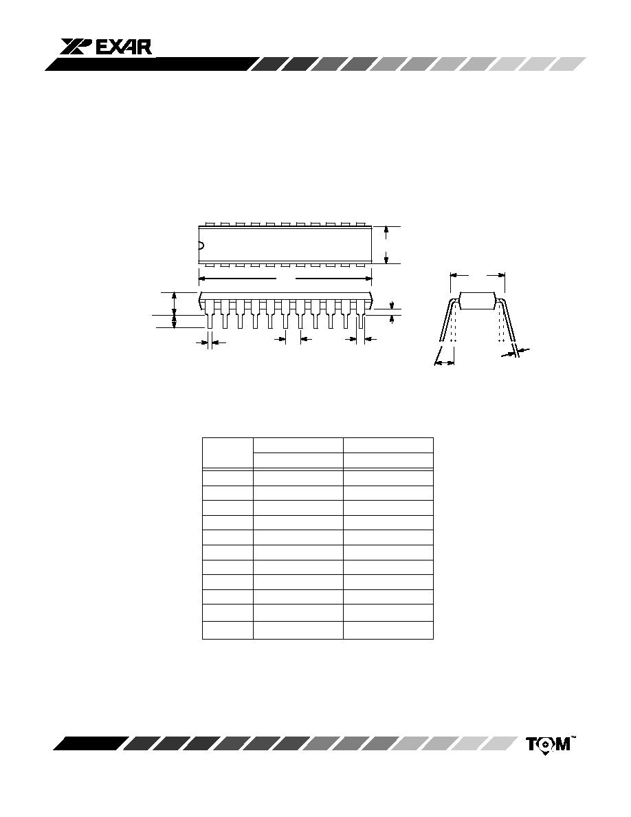
22 LEAD PLASTIC DUAL-IN-LINE
(400 MIL PDIP)
22
1
12
11
D
e
B
1
A
1
E
1
C
E
A
L
B
Seating
Plane
SYMBOL
MIN
MAX
MIN
MAX
INCHES
A
0.145
0.210
3.68
5.33
A
1
0.015
0.070
0.38
1.78
B
0.014
0.024
0.36
0.56
B
1
0.030
0.070
0.76
1.78
C
0.008
0.016
0.20
0.38
D
1.050
1.120
26.67
28.45
E
0.390
0.425
9.91
10.80
E
1
0.330
0.380
8.38
9.65
e
0.100 BSC
2.54 BSC
L
0.115
0.160
2.92
4.06
0
∞
15
∞
0
∞
15
∞
MILLIMETERS
XR-T6165
14
Rev. 2.02
SYMBOL
MIN
MAX
MIN
MAX
A
0.093
0.104
2.35
2.65
A1
0.004
0.012
0.10
0.30
B
0.013
0.020
0.33
0.51
C
0.009
0.013
0.23
0.32
D
0.598
0.614
15.20
15.60
E
0.291
0.299
7.40
7.60
e
0.050 BSC
1.27 BSC
H
0.394
0.419
10.00
10.65
L
0.016
0.050
0.40
1.27
INCHES
MILLIMETERS
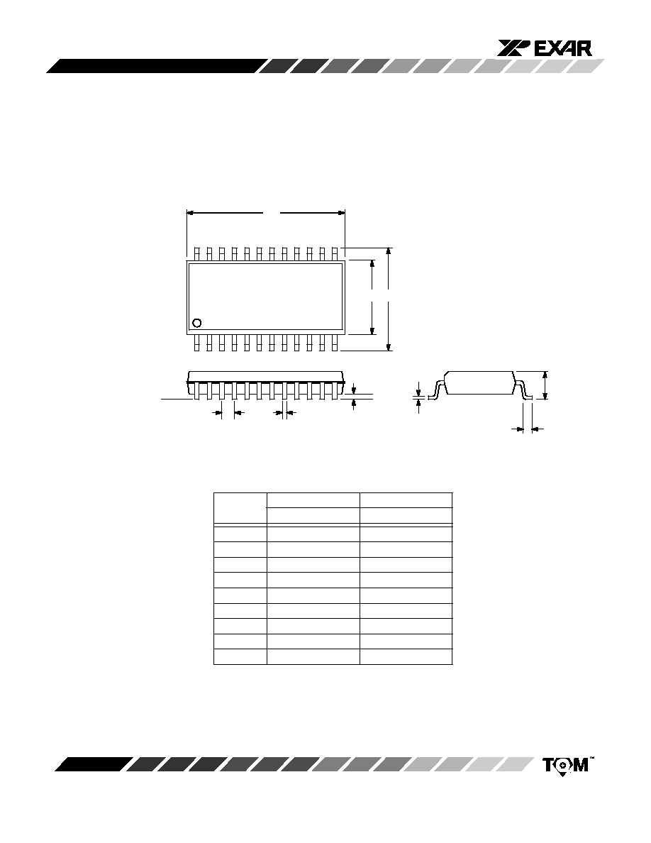
24 LEAD SMALL OUTLINE
(300 MIL JEDEC SOIC)
e
D
E
H
B
A
L
C
A
1
Seating
Plane
24
13
12

XR-T6165
15
Rev. 2.02
Notes

XR-T6165
16
Rev. 2.02
NOTICE
EXAR Corporation reserves the right to make changes to the products contained in this publication in order to im-
prove design, performance or reliability. EXAR Corporation assumes no responsibility for the use of any circuits de-
scribed herein, conveys no license under any patent or other right, and makes no representation that the circuits are
free of patent infringement. Charts and schedules contained herein are only for illustration purposes and may vary
depending upon a user's specific application. While the information in this publication has been carefully checked;
no responsibility, however, is assumed for inaccuracies.
EXAR Corporation does not recommend the use of any of its products in life support applications where the failure or
malfunction of the product can reasonably be expected to cause failure of the life support system or to significantly
affect its safety or effectiveness. Products are not authorized for use in such applications unless EXAR Corporation
receives, in writing, assurances to its satisfaction that: (a) the risk of injury or damage has been minimized; (b) the
user assumes all such risks; (c) potential liability of EXAR Corporation is adequately protected under the circum-
stances.
Copyright 1990 EXAR Corporation
Datasheet June 1997
Reproduction, in part or whole, without the prior written consent of EXAR Corporation is prohibited.