 | ÐлекÑÑоннÑй компоненÑ: XRT71D04 | СкаÑаÑÑ:  PDF PDF  ZIP ZIP |
Äîêóìåíòàöèÿ è îïèñàíèÿ www.docs.chipfind.ru
Exar
Corporation 48720 Kato Road, Fremont CA, 94538
·
(510) 668-7000
·
FAX (510) 668-7017
·
www.exar.com
áç
áç
áç
áç
XRT71D04
4 CHANNEL E3/DS3/STS-1 JITTER ATTENUATOR, STS-1 TO DS3 DESYNCHRONIZER
APRIL 2001
REV. 1.1.1
GENERAL DESCRIPTION
The XRT71D04 is a four channel, single chip Jitter At-
tenuator, that meets the Jitter transfer characteristic
requirements specified in the ETSI TBR-24, Bellcore
GR-499 and GR-253 standards.
In addition, the XRT71D04 also meets the Jitter and
Wander specifications described in the ANSI
T1.105.03b 1997, Bellcore GR-253 and GR-499 stan-
dards for Desynchronizing and Pointer adjustments in
the DS3 to STS-SPE mapping applications.
FEATURES
· Meets the E3/DS3/STS-1 jitter requirements
· No external components required
· Compliant with jitter transfer template outlined in
ITU G.751, G.752, G.755, GR-499-CORE,1995
GR-253-CORE standards
· Meets output jitter requirement as specified by
ETSI TBR24
· Meets the Jitter and Wander specifications
described in T1.105.03b,GR-253 and GR-499 stan-
dards
· Selectable buffer size of 16 and 32 bits
· Jitter attenuator can be disabled
· Available in a 80 pin TQFP package
· Single 3.3V or 5.0V supply.
· Operates over - 40
0
C to 85
0
C temperature range.
APPLICATIONS
· E3/DS3 Access Equipment
· STS-SPE to DS3 Mapper
· DSLAMs
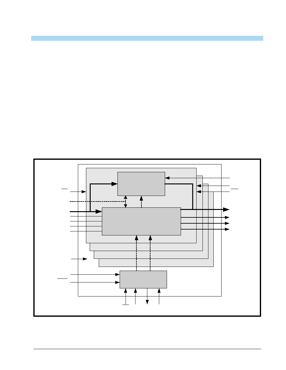
F
IGURE
1. B
LOCK
D
IAGRAM
(
ONE
CHANNEL
)
DS3/E3_n
Microprocessor Serial
Interface
HOST
Reset
XRT71D04
n = 0, 1, 2, 3
16/32 Bit FIFO
Timing Control Block /
Phase locked Loop
Write Clock
Read Clock
RRCLK_n
RRPOS_n
RRNEG_n
FL_n
DJA_n
RClk_n
RClkES
RPOS_n
RNEG_n
FSS
MCLK_n
STS1_n
Channel 0
Channel 1
Channel 2
Channel 3
ICT
CS SDI SDO SClk
MODE_CTRL
XRT71D04
áç
áç
áç
áç
4 CHANNEL E3/DS3/STS-1 JITTER ATTENUATOR, STS-1 TO DS3 DESYNCHRONIZER
REV. 1.1.1
2
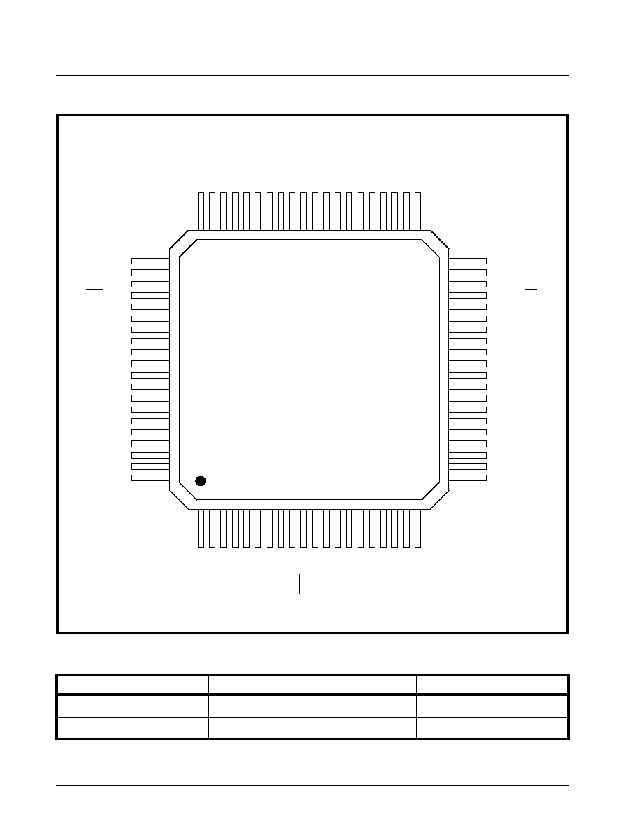
F
IGURE
2. P
IN
O
UT
OF
THE
XRT71D04
AGND
FL_1
STS1_1
DS3/E3_3
DJA_3
MCLK_1
GND
RCLK_1
RPOS_1
RNEG_1
VDD
RNEG_0
RPOS_0
RCLK_0
GND
MCLK_0
DJA_1/SDI
STS1_3
FL_3
AGND
AVDD
NC
GND
RRCLK_0
RRPOS_0
RRNEG_0
RRCLKES
NC
Reset
DS3/E3_1
VDD
MODE_CTRL
ICT
HOST
FLRST
RRNEG_3
RRPOS_3
RRCLK_3
GND
AVDD
AVDD
NC
GND
RRCLK_1
RRPOS_1
RRNEG_1
NC
RCLKES
NC
VDD
DS3/E3_2
SDO
FSS
NC
RRNEG_2
RRPOS_2
RRCLK_2
GND
NC
AVDD
XRT71D04
1
2
3
4
5
6
7
8
9
10
11
12
13
14
15
16
17
18
19
20
60
59
58
57
56
55
54
53
52
51
50
49
48
47
46
45
44
43
42
41
61
62
63
64
65
66
67
68
69
70
71
72
73
74
75
76
77
78
79
80
AGND
FL_2
STS1_2
DJA_2/CS
MCLK_2
GND
RCLK_2
RPOS_3
RNEG_3
VDD
RNEG_2
RPOS_2
RCLK_3
GND
MCLK_3
DJA_0/SCLK
DS3/E3_0
STS1_0
FL_0
AGND
40
39
38
37
36
35
34
33
32
31
30
29
28
27
26
25
24
23
22
21
ORDERING INFORMATION
P
ART
N
UMBER
P
ACKAGE
O
PERATING
T
EMPERATURE
R
ANGE
XRT71D04IV
80 Pin TQFP
-40
o
C to +85
o
C
T
HERMAL
I
NFORMATION
Theta - J
A
= ° C/W
Theta J
C
= ° C/W

áç
áç
áç
áç
XRT71D04
4 CHANNEL E3/DS3/STS-1 JITTER ATTENUATOR STS-1 TO DS3 DESYNCHRONIZER
REV. 1.1.1
I
TABLE OF CONTENTS
GENERAL DESCRIPTION .................................................................................................. 1
F
EATURES
................................................................................................................................................... 1
A
PPLICATIONS
............................................................................................................................................. 1
Figure 1. Block Diagram (one channel) ................................................................................................. 1
Figure 2. Pin Out of the XRT71D04 ........................................................................................................ 2
ORDERING INFORMATION ..................................................................................................................... 2
TABLE OF CONTENTS...................................................................................................................................... I
PIN DESCRIPTIONS ........................................................................................................... 3
ELECTRICAL CHARACTERISTICS ................................................................................... 9
Figure 3. Input/Output Timing ................................................................................................................ 9
Figure 4. Timing Diagram for the Microprocessor Serial Interface .................................................. 10
SYSTEM DESCRIPTION ................................................................................................... 12
Figure 5. A typical Channel_n of the XRT71D04 configured to operate in the Hardware Mode . 12
Figure 6. A typical Channel_n of the XRT71D04 configured to operate in the Host Mode ........... 13
1.0 Jitter Attenuator PLL .............................................................................................................................. 13
1.1 B
ACKGROUND
I
NFORMATION
...................................................................................................................................... 13
1.1.1 Definition of Jitter ..........................................................................................................................................13
1.1.2 SONET STS-1 to DS3 Mapping ....................................................................................................................13
1.2 J
ITTER
T
RANSFER
C
HARACTERISTICS
......................................................................................................................... 13
Figure 7. Category 1 DS3 Jitter Transfer Mask .................................................................................. 14
1.2.1 Jitter Tolerance ............................................................................................................................................. 14
1.2.2 Jitter Generation............................................................................................................................................ 14
1.2.3 Jitter Attenuation ........................................................................................................................................... 14
1.2.4 SONET STS-1 DS3 Mapping ....................................................................................................................... 14
Figure 8. XRT71D04 Desynchronizer Block Diagram ........................................................................ 15
1.3 XRT71D
O
4 J
ITTER
T
RANSFER
C
HARACTERISTICS
...................................................................................................... 16
T
ABLE
1: XRT71D04 J
ITTER
T
RANSFER
F
UNCTION
.................................................................................. 16
T
ABLE
2: XRT71D04 M
AXIMUM
J
ITTER
T
OLERANCE
................................................................................. 17
2.0 Operating Modes .................................................................................................................................... 17
2.1 H
ARDWARE
M
ODE
.....................................................................................................................................................17
T
ABLE
3: F
UNCTIONS
OF
DUAL
MODE
PINS
IN
H
ARDWARE
M
ODE
CONFIGURATION
..................................... 17
2.2 H
OST
M
ODE
:............................................................................................................................................................ 17
T
ABLE
4: A
DDRESS
AND
B
IT
F
ORMATS
OF
THE
C
OMMAND
R
EGISTERS
...................................................... 18
3.0 Microprocessor Serial Interface ............................................................................................................ 18
3.1 S
ERIAL
I
NTERFACE
O
PERATION
.................................................................................................................................. 18
3.1.1 Bit 1--R/W (Read/Write) Bit ..........................................................................................................................18
3.1.2 Bits 2 through 6--A0, A1, A2 ,A3, and A4 .................................................................................................... 18
3.1.3 Bit 7--A5 ....................................................................................................................................................... 18
3.1.4 Bit 8--A6 ....................................................................................................................................................... 18
3.1.5 Read Operation ............................................................................................................................................. 18
3.1.6 Write Operation ............................................................................................................................................. 18
Figure 9. Microprocessor Serial Interface Data Structure ................................................................. 19
3.1.7 Simplified Interface Option ............................................................................................................................ 19
Figure 10. Timing Diagram for the Microprocessor Serial Interface ................................................ 19
ORDERING INFORMATION ............................................................................................. 20
PACKAGE DIMENSIONS ................................................................................................. 20
R
EVISION
H
ISTORY
..................................................................................................................................... 21
XRT71D04
áç
áç
áç
áç
4 CHANNEL E3/DS3/STS-1 JITTER ATTENUATOR, STS-1 TO DS3 DESYNCHRONIZER
REV. 1.1.1
3
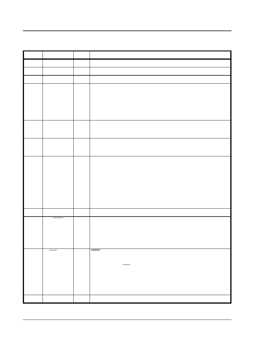
PIN DESCRIPTIONS
PIN DESCRIPTION
P
IN
#
N
AME
T
YPE
D
ESCRIPTION
1
AVDD
****
Analog Power Supply = 5V±5% or 3.3V±5%
2
NC
No Connection
3
GND
****
Digital Ground
4
RRCLK_0
O
Received Recovered Output (De-jittered) Clock - channel 0:
Output is the de-jittered or smoothed clock if the jitter attenuator is enabled. The
de-jittered data, RRPOS/RRNEG are clocked to this signal.
If RRCLKES is "low", RRPOS/RRNEG will be updated at the falling edge of
RRCLK.
If RRCLKES is "high", RRPOS/RRNEG will be updated at the rising edge of
RRCLK.
5
RRPOS_0
O
Received Recovered Positive Data (De-Jittered) Output - channel 0:
De-jittered positive data output. Updated on the rising or falling edge of RRCLK,
depending upon the state of the RRCLKES input pin (or bit-field setting).
6
RRNEG_0
O
Received Recovered Negative Data (De-Jittered) Output - channel 0:
De-jittered negative data output. Updated on the rising or falling edge of RRCLK,
depending upon the state of the RRCLKES input pin (or bit-field setting).
7
RRCLKES
I
Received Recovered Clock Edge Select Input:
Hardware Mode:
1. When RRCLKES = "0", then RRPOS and RRNEG are updated on the falling
edge of RRCLK
2. When RRCLKES = "1", then RRPOS and RRNEG are updated on the rising
edge of RRCLK
N
OTE
: This applies to all channels.
Host Mode
Connect this pin to GND when the 71D04 is configured in the Host Mode.
Internal 50 K Ohm pull-down resistor.
8
NC
No Connection
9
Reset
I
Reset Input.
(Active-Low):
A high-low transition will re-center the internal FIFO, and will clear the Command
Registers (for Host Mode operation). Resetting this pin may corrupt data within
the device.
For normal operation, pull this pin to VDD.
Internal 50 K Ohm pull-up resistor.
10
DS3/E3_1
I
DS3/E3 Select Input - channel 1
:
This pin along with the STS-1 mode select pin selects the operating mode. The
following table provides the configuration:
STS-1 DS3/E3 XRT71D04 Operating Mode
0 0 DS3 (44.736 MHz)
0 1 E3 (34.368 MHz)
1 0 STS-1 (51.84 MHz)
1 1 E3 (34.368 MHz)
Internal 50 K Ohm pull-down resistor.
11
VDD
****
Digital Power Supply = 5V±5% or 3.3V±5%
áç
áç
áç
áç
XRT71D04
4 CHANNEL E3/DS3/STS-1 JITTER ATTENUATOR, STS-1 TO DS3 DESYNCHRONIZER
REV. 1.1.1
4
12
MODE_CTRL
I
Mode Control:
When "High" in Multimode, all channels are independent. When "Low", the Mas-
ter Channel (channel_0) controls DS3/E3_n, STS1_n, RCLKES, FSS and
MCLK_n. DJA is NOT affected.
Internal 50 K Ohm pull-up resistor.
13
ICT
I
In Circuit Testing Input.
(Active low):
With this pin tied to ground, all output pins will be in high impedance mode for in-
circuit-testing.
For normal operation this input pin should be tied to VDD.
Internal 50 K Ohm pull-up resistor.
14
HOST
I
Host/Hardware Mode Select:
An active-high input enables the Host mode. Data is written to the command reg-
isters to configure the XRT71D04.
In the Host mode, the states of discrete input pins are inactive.
An active-low input enables the Hardware Mode.In this mode, the discrete inputs
are active.
Internal 50 K Ohm pull-down resistor.
15
FLRST
I
FIFO Limit Reset
Hardware Mode
Whenever the FIFO is within 2 bits of either underflow or overflow, the FL_n will
be set high.
This pin allows the user to reset the state of FL_n, (FIFO Limit) output pin.
This pin when pulsed "High", resets the the FL_n output pin, (toggles to GND).
N
OTE
: The FL_n could be set "High" again if the FIFO is within 2 bits of either
underflow or overflow.
Host Mode
Reading the FL_n bits in the status registers clears this FL_n pin. Master Reset
also clears the FL_n output.
This pin is tied to GND. FLRST has no effect in this mode.
Internal 50 K Ohm pull-down resistor.
16
RRNEG_3
O
Received Recovered Negative Data (De-Jittered) Output - channel 3:
See description of pin 6
17
RRPOS_3
O
Received Positive Data (De-Jittered) Output - channel 3:
See description of pin 5
18
RRCLK_3
O
Received Recovered Output (De-jittered) Clock - channel 3:
See description of pin 4
19
GND
O
Digital Ground
20
AVDD
****
Analog Power Supply = 5V±5% or 3.3V±5%
21
AGND
****
Analog Ground
22
FL_0
O
FIFO Limit - channel 0:
This output pin is driven high whenever the internal FIFO comes within two-bits of
being either underflow or overflow.
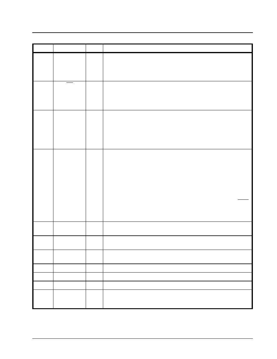
PIN DESCRIPTION
P
IN
#
N
AME
T
YPE
D
ESCRIPTION
Document Outline