 | –≠–ª–µ–∫—Ç—Ä–æ–Ω–Ω—ã–π –∫–æ–º–ø–æ–Ω–µ–Ω—Ç: XRT7245 | –°–∫–∞—á–∞—Ç—å:  PDF PDF  ZIP ZIP |
Document Outline
- GENERAL DESCRIPTION
- Features
- Applications
- Ordering Information
- Functional Description
- The Receive Section
- The Transmit Section
- The Microprocessor Interface Section
- Performance Monitor Section
- Test and Diagnostic Section
- Line Interface Drive and Scan Section
- FEATURES
- Transmit and Receive Sections
- PIN DESCRIPTION�
- DC ELECTRICAL CHARACTERISTICS
- AC ELECTRICAL CHARACTERISTICS�
- Interfacing to the ATM Switch (ATM Layer �Processor)
- Interfacing to the Local Microprocessor
- Interfacing the UNI to the DS3 Line
- PRINCIPLE OF OPERATION
- Reading Performance Monitor (PMON) �Registers
- For Example
- The PMON Holding Register
- In Summary: Whenever an ç8-bité µC/µP needs to read a PMON Register, it must execute the followin...
- 3.2.2 Data Access Modes
- Figure 8. Behavior of Microprocessor Interface signals during an çIntel-typeé Programmed I/O Read...
- Figure 9. Behavior of the Microprocessor Interface Signals, during an çIntel-typeé Programmed I/O...
- Figure 10. Illustration of the Behavior of Microprocessor Interface signals, during a çMotorola- ...
- Figure 11. Illustration of the Behavior of the Microprocessor Interface signal, during a �çMotoro...
- Figure 12. Behavior of the Microprocessor Interface Signals, during the çInitialé Read Operation ...
- Figure 13. Behavior of the Microprocessor Interface Signals, during subsequent çReadé Operations ...
- Figure 14. Behavior of the Microprocessor Interface signals, during the çInitialé Write Operation...
- Figure 15. Behavior of the Microprocessor Interface Signals, during subsequent çWriteé �Operation...
- Figure 16. Behavior of the Microprocessor Interface Signals, during the çInitialé Read Operation ...
- Figure 17. Behavior the Microprocessor Interface Signals, during subsequent çReadé Operations wit...
- Figure 18. Behavior of the Microprocessor Interface signals, during the çInitialé Write Operation...
- Figure 19. Behavior of the Microprocessor Interface Signals, during subsequent çWriteé �Operation...
- 3.3 On-Chip Register Organization
- Address = 00h, UNI Operating Mode Register
- Bit 7ÑLine Loop Back Mode
- Bit 6ÑCell Loop Back Mode
- Bit 5ÑPLCP Loop Back Mode
- Bit 4ÑReset
- Bit 3ÑDirect Mapped ATM/PLCP Mode* Selection
- Bit 2ÑM13/C-Bit* (DS3 Frame Format) Selection
- Bits 1, 0ÑTimRefSel[1, 0] (Timing Reference �SelectÑTransmit PLCP Processor and Transmit DS3 Framer)
- Address = 01h, UNI I/O Control Register
- Bit 7ÑLOC (Loss of Clock)Enable
- Bit 6ÑTest PMON
- Bit 5ÑInt En Reset (Automatic Reset of Interrupt Enable Bits) Select
- Bit 4ÑAMI/B3ZS* (Line Code)
- Bit 3ÑUnipolar/Bipolar* (Line Code)
- Bit 2ÑTxLineClk Inv
- Bit 1ÑRxLineClk Inv
- Bit 0ÑReframe (Receive DS3 Framer)
- Address = 02h, Part Number Register
- Address = 03h, Version Number Register
- Address = 04h, UNI Interrupt Enable Register
- Bit 7ÑRx DS3 Interrupt Enable
- Bit 6ÑRx PLCP Interrupt Enable
- Bit 5ÑRx CP Interrupt Enable
- Bit 4ÑRx UTOPIA Interrupt Enable
- Bit 3ÑTx UTOPIA Interrupt Enable
- Bit 2ÑTx CP Interrupt Enable
- Bit 1ÑTx DS3 Framer Interrupt Enable
- Bit 0ÑOne Second Interrupt Enable
- Address = 05h, UNI Interrupt Status Register
- Bit 7ÑRx DS3 (Framer) Interrupt Status
- Bit 6ÑRx PLCP Interrupt Status
- Bit 5ÑRx CP (Cell Processor) Interrupt Status
- Bit 4ÑRx UTOPIA Interrupt Status
- Bit 3ÑTx UTOPIA Interrupt Status
- Bit 2ÑTx CP (Cell Processor) Interrupt Status
- Bit 1ÑTx DS3 (Framer) Interrupt Status
- Bit 0ÑOne Second Interrupt Status
- Address = 06h, Test Cell Control and Status Register
- Bit 4ÑTest Cell (Generator/Receiver) Enable
- Bit 3ÑLine*/System (Side Testing)
- Bit 2ÑOne Shot Test
- Bit 1ÑOne Shot Done
- Bit 0ÑPRBS (Pseudo-Random Byte Sequence) Lock
- Address = 07h, Future Use
- Address = 08h, Test Cell Header Byte-1
- Address = 09h, Test Cell Header Byte-2
- Address = 0Ah, Test Cell Header Byte-3
- Address = 0Bh, Test Cell Header Byte-4
- Address = 0Ch, Test Cell Error AccumulatorÑMSB
- Address = 0Dh, Test Cell Error AccumulatorÑLSB
- Address = 0Eh, Rx DS3 Configuration and Status Register
- Bit 7ÑRxAISÑReceive AIS Signal
- Bit 6ÑRxLOSÑReceive LOS Condition
- Bit 5ÑRxIdleÑReceive Idle Condition
- Bit 4ÑRxOOFÑOut of Frame Condition
- Bit 3ÑInt (Receive DS3 Framer) LOS Disable
- Bit 2ÑFraming On Parity
- Bit 1ÑFSync Algo
- Bit 0ÑMSync Algo
- Address = 0Fh, Rx DS3 Status Register
- Bit 4ÑRxFERF (Far End Receive Failure)
- Bit 3ÑRxAIC
- Bits 2-0 RxFEBE[2:0]
- Address = 10h, Rx DS3 Interrupt Enable Register
- Bit 7ÑCP Bit Error Interrupt Enable
- Bit 6ÑLOS Interrupt Enable
- Bit 5ÑAIS Interrupt Enable
- Bit 4ÑIdle (Condition) Interrupt Enable
- Bit 3ÑFERF Interrupt Enable
- Bit 2ÑAIC Interrupt Enable
- Bit 1ÑOOF Interrupt Enable
- Bit 0ÑParity Error Interrupt Enable
- Address = 11h, RxDS3 Interrupt Status Register
- Bit 7ÑCP Bit Error Interrupt Status
- Bit 6ÑLOS Interrupt Status
- Bit 5ÑAIS Interrupt Status
- Bit 4ÑIdle Interrupt Status
- Bit 3ÑFERF Interrupt Status
- Bit 2Ñ(Change in) AIC Interrupt Status
- Bit 1ÑOOF (Receive DS3 Framer) Interrupt Status
- Bit 0ÑP-Bit Error (Receive DS3 Framer) Interrupt Status
- Address = 12h, RxDS3 FEAC Register
- Address = 13h, RxDS3 FEAC Interrupt Enable/Status Register
- Bit 4ÑFEAC Valid
- Bit 3ÑRxFEAC Remove Interrupt Enable
- Bit 2ÑRxFEAC Remove Interrupt Status
- Bit 1ÑRxFEAC Valid Interrupt Enable
- Bit 0ÑRxFEAC Valid Interrupt Status
- Address = 14h, RxDS3 LAPD Control Register
- Bits 7Ö3 Enable5 F(4)ÖF(0)
- Bit 2 RxLAPD Enable
- Bit 1 RxLAPD (Message Frame Reception �Complete) Interrupt Enable
- Bit 0 RxLAPD (Message Reception Complete) �Interrupt Status
- Address = 15h, Rx DS3 LAPD Status Register
- Bit 6ÑRxAbort (Receive Abort Sequence)
- Bits, 5 and 4ÑRxLAPDType[1, 0]
- Bit 3ÑRxCR (Command/Response) Type
- Bit 2ÑRx FCS (Frame Check Sequence) Error
- Bit 1ÑEnd Of Message
- Bit 0ÑFlag Present
- Address = 16h, Tx DS3 Configuration Register
- Bit 7ÑTx Yellow Alarm
- Bit 6ÑTx X-Bit (Force X bits to ç1é)
- Bit 5ÑTx Idle (Pattern)
- Bit 4ÑTx AIS (Pattern)
- Bit 3ÑTx LOS (Loss of Signal)
- Bit 2ÑFERF on LOS
- Bit 1ÑFERF on OOF
- Bit 0ÑFERF on AIS
- Address = 17h, Tx DS3 M-Bit Mask Register
- Bit 7-5: TxFEBEDat[2:0]
- Bit 4ÑFEBE Register Enable
- Bit 3ÑTransmit Erred P-Bit
- Bit 2Ö0 M-Bit Mask[2:0]
- Address = 18h, Tx DS3 F-Bit Mask1 Register
- Bits 3Ö0 F-Bit Mask[27:24]
- Address = 19h, Tx DS3 F-Bit Mask2 Register
- Bits 7Ö0 F-Bit Mask[23:16]
- Address = 1Ah, Tx DS3 F-Bit Mask3 Register
- Bits 7Ö0 F-Bit Mask[15:8]
- Address = 1Bh, Tx DS3 F-Bit Mask4 Register
- Bits 7Ö0 F-Bit Mask[7:0]
- Address = 1Ch, Tx DS3 FEAC Configuration and Status Register
- Bit 4ÑTxFEAC Interrupt Enable
- Bit 3ÑTxFEAC Interrupt Status
- Bit 2ÑTxFEAC Enable
- Bit 1ÑTxFEAC Go
- Bit 0ÑTxFEAC Busy
- Address = 1Dh, Tx DS3 FEAC Register
- Address = 1Eh, Tx DS3 LAPD Configuration Register
- Bit 3ÑAuto Retransmit
- Bit 2:1 = TxLAPD Type[1, 0]
- Bit 0ÑTxLAPD Enable
- Address = 1Fh, Tx DS3 LAPD Status/Interrupt Register
- Bit 3ÑTxDL Start
- Bit 2ÑTxDL Busy
- Bit 1ÑTxLAPD Interrupt Enable
- Bit 0ÑTxLAPD Interrupt Status
- Address = 20h, PMON LCV Event Count RegisterÑMSB
- Address = 21h, PMON LCV Event Count RegisterÑLSB
- Address = 22h, PMON Framing Bit Error Event Count RegisterÑMSB
- Address = 23h, PMON Framing Bit Error Event Count RegisterÑLSB
- Address = 24h, PMON Parity Error Event Count RegisterÑMSB
- Address = 25h, PMON Parity Error Event Count RegisterÑLSB
- Address = 26h, PMON FEBE Event Count RegisterÑMSB
- Address = 27h, PMON FEBE Event Count RegisterÑLSB
- Address = 28h, PMON BIP-8 Error Count RegisterÑMSB
- Address = 29h, PMON BIP-8 Error Count RegisterÑLSB
- Address = 2Ah, PMON PLCP Framing Byte Error Count RegisterÑMSB
- Address = 2Bh, PMON PLCP Framing Byte Error Count RegisterÑLSB
- Address = 2Ch, PMON PLCP FEBE Count RegisterÑMSB
- Address = 2Dh, PMON PLCP FEBE Count RegisterÑLSB
- Address = 2Eh, PMON Received Single HEC Error CountÑMSB
- Address = 2Fh, PMON Received Single HEC Error CountÑLSB
- Address = 30h, PMON Received Multiple-Bit HEC ErrorÑMSB
- Address = 31h, PMON Received Multiple-Bit HEC ErrorÑLSB
- Address = 32h, PMON Received Idle Cell CountÑMSB
- Address = 33h, PMON Received Idle Cell CountÑLSB
- Address = 34h, PMON Received Valid Cell CountÑMSB
- Address = 35h, PMON Received Valid Cell CountÑLSB
- Address = 36h, PMON Discarded Cell CountÑMSB
- Address = 37h, PMON Discarded Cell CountÑLSB
- Address = 38h, PMON Transmitted Idle Cell CountÑMSB
- Address = 39h, PMON Transmitted Idle Cell CountÑLSB
- Address = 3Ah, PMON Transmitted Valid Cell CountÑMSB
- Address = 3Bh, PMON Transmitted Valid Cell CountÑLSB
- Address = 3Ch, PMON Holding Register
- Address = 3Dh, One Second Error Status Register
- Bit 1ÑErrored Second
- Bit 0ÑSevere Errored Second
- Address = 3Eh, LCVÑOne Second Accumulator RegisterÑMSB
- Address = 3Fh, LCVÑOne Second Accumulator RegisterÑLSB
- Address = 40h, Frame Parity ErrorsÑOne Second Accumulator RegisterÑMSB
- Address = 41h, Frame Parity ErrorsÑOne Second Accumulator RegisterÑLSB
- Address = 42h, HEC ErrorsÑOne Second Accumulator RegisterÑMSB
- Address = 43h, HEC ErrorsÑOne Second Accumulator RegisterÑLSB
- Address = 44h, Rx PLCP Configuration/Status Register
- Bit 3ÑReframe (Receive PLCP Processor)
- Bit 2ÑPOOF (Receive PLCP OOF Condition) Status
- Bit 1ÑPLOF (Receive PLCP LOF Condition) Status
- Bit 0ÑYellow Status
- Address = 45h, Rx PLCP Interrupt Enable Register
- Bit 1ÑPOOF Interrupt Enable
- Bit 0ÑPLOF Interrupt Enable
- Address = 46h, Rx PLCP Interrupt Status Register
- Bit 1ÑPOOF Interrupt Status
- Bit 0ÑPLOF Interrupt Status
- Address = 47h, Future Use
- Address = 48h, Tx PLCP A1 Byte Error Mask
- Address = 49h, Tx PLCP A2 Byte Error Mask
- Address = 4Ah, Tx PLCP B1 Byte (BIP-8) Error Mask
- Address = 4Bh, Tx PLCP G1 Byte Register
- Bit 4ÑTxFEBE Mask
- Bit 3ÑYellow Alarm
- Bit 2Ñ0ÑLSS(2:0)
- Address = 4Ch, Rx CP Configuration Register
- Bit 7ÑRxLCD (Loss of Cell Delineation)
- Bit 6ÑRDPChk (Receive çData Path Integrity Checké)Pattern
- Bit 5ÑRDPChk (Receive çData Path Integrity Checké) Pattern Enable
- Bit 4ÑIC (Idle Cell) Discard
- Bit 3ÑOAM Check Bit
- Bit 2ÖDe-Scramble Enable
- Bit 1ÑRx Coset Enable
- Bit 0ÑHEC Error Ignore
- Address = 4Dh, Rx CP Additional Configuration Register
- Bit 5ÑUser Cell Filter Discard
- Bit 4ÑUser Cell Filter Enable
- Bits 3 and 2ÑCorrection Threshold[1, 0]
- Bit 1ÑCorrection Enable
- Address = 4Eh, Rx CP Interrupt Enable Register
- Bit 2ÑOAM (Cell Received) Interrupt Enable
- Bit 1ÑLCD (Loss of Cell Delineation) Interrupt Enable
- Bit 0ÑHEC Byte Error Interrupt Enable
- Address = 4Fh, Rx CP Interrupt Status Register
- Bit 2ÑOAM (Cell Received) Interrupt Status
- Bit 1ÑLCD (Loss of Cell Delineation) Interrupt Status
- Bit 0ÑHEC Byte Error Interrupt Status
- Address = 50h, Rx CP Idle Cell Pattern HeaderÑByte 1
- Address = 51h, Rx CP Idle Cell Pattern HeaderÑByte 2
- Address = 52h, Rx CP Idle Cell Pattern HeaderÑByte 3
- Address = 53h, Rx CP Idle Cell Pattern HeaderÑByte 4
- Address = 54h, Rx CP Idle Cell Mask HeaderÑByte 1
- Address = 55h, Rx CP Idle Cell Mask HeaderÑByte 2
- Address = 56h, Rx CP Idle Cell Mask HeaderÑByte 3
- Address = 57h, Rx CP Idle Cell Mask HeaderÑByte 4
- Address = 58h, Rx CP User Cell Filter Pattern HeaderÑByte 1
- Address = 59h, Rx CP User Cell Filter Pattern HeaderÑByte 2
- Address = 5Ah, Rx CP User Cell Filter Pattern HeaderÑByte 3
- Address = 5Bh, Rx CP User Cell Filter Pattern HeaderÑByte 4
- Address = 5Ch, Rx CP User Cell Filter Mask HeaderÑByte 1
- Address = 5Dh, Rx CP User Cell Filter Mask HeaderÑByte 2
- Address = 5Eh, Rx CP User Cell Filter Mask HeaderÑByte 3
- Address = 5Fh, Rx CP User Cell Filter Mask HeaderÑByte 4
- Address = 60h, Tx CP Control Register
- Bit 7ÑScrambler Enable
- Bit 6ÑCoset Enable
- Bit 5ÑHEC Byte Insert EnableÑAssigned Cells
- Bit 4ÑTDPChk Pat (Transmit Data Path Integrity Check Pattern Selection)
- Bit 3ÑGFC Nibble-Field Insert Enable
- Bit 2ÑTDP (Transmit Data Path Integrity Test) �Error Interrupt Enable
- Bit 1ÑIC (Idle Cell) HEC Byte Calculation Enable
- Bit 0ÑTDP (Transmit Data Path Integrity Check) Error Interrupt Status
- Address = 61h, Tx CP OAM Cell Register
- Bit 7ÑSend OAM (Cell)
- Address = 62h, Tx CP HEC Byte Error Mask Register
- Address = 63h, Future Use
- Address = 64h, Tx CP Idle Cell Pattern HeaderÑByte 1
- Address = 65h, Tx CP Idle Cell Pattern HeaderÑByte 2
- Address = 66h, Tx CP Idle Cell Pattern HeaderÑByte 3
- Address = 67h, Tx CP Idle Cell Pattern HeaderÑByte 4
- Address = 68h, Tx CP Idle Cell Pattern HeaderÑByte 5
- Address = 69h, Tx CP Idle Cell Payload Register
- Address = 6Ah, UTOPIA Configuration Register
- Bit 5ÑHandshake Mode
- Bit 4ÑM-PHY/S-PHY* (UTOPIA Operating Mode)
- Bit 3ÑCellOf52Bytes
- Bits 2, 1,ÑTFIFODepth[1, 0]
- Bit 0ÑUtWidth16ÑUTOPIA Data Width
- Address = 6Bh, Receive UTOPIA Interrupt Enable/Status Register
- Bit 6ÑRxFIFO Reset
- Bit 5ÑRxFIFO Overrun Interrupt Enable
- Bit 4ÑRxFIFO Underrun Interrupt Enable
- Bit 3ÑRxFIFO Change of Cell Alignment Interrupt Enable
- Bit 2ÑRxFIFO Overrun Interrupt Status
- Bit 1ÑRxFIFO Underrun Interrupt Status
- Bit 0ÑRxFIFO Change of Cell Alignment Interrupt Status
- Address = 6Ch, Receive UTOPIA Address Register
- Address = 6Dh, Receive UTOPIA FIFO Status Register
- Bit 1ÑRxFIFO Full
- Bit 0ÑRxFIFO Empty
- Address = 6Eh, Transmit UTOPIA Interrupt/Status Register
- Bit 7ÑTxFIFO Reset
- Bit 6ÑDiscard (Cell) Upon Parity Error (Transmit UTOPIA Interface block)
- Bit 5ÑTx Parity Interrupt Enable (Transmit UTOPIA Interface block)
- Bit 4ÑTxFIFO Overrun Interrupt Enable
- Bit 3ÑTxFIFO Change of Cell Alignment Interrupt Enable
- Bit 2ÑTx Parity Interrupt Status
- Bit 1ÑTxFIFO Overrun Interrupt Status
- Bit 0ÑTxFIFO Change of Cell Alignment Interrupt Status
- Address = 6Fh, Transmit UTOPIA UDF2 Register
- Address = 70h, Transmit UTOPIA Address Register
- Address = 71h, Transmit UTOPIA FIFO Status Register
- Bit 1ÑTxFIFO Full
- Bit 0ÑTxFIFO Empty
- Address = 72h, Line Interface Drive Register
- Bit 5ÑREQB (Receive Equalization Bypass �Control)
- Bit 4ÑTAOS (Transmit All Ones Signal)
- Bit 3ÑEncodis (B3ZS Encoder Disable)
- Bit 2ÑTxLev (Transmit Output Line Build-Out �Select Output)
- Bit 1ÑRLOOP (Remote Loop-back)
- Bit 0ÑLLOOP
- Address = 73h, Line Interface Scan Register
- Bit 2ÑDMO (Drive Monitor Output)
- Bit 1ÑRLOL (Receive Loss of Lock)
- Bit 0ÑRLOS (Receive Loss of Signal)
- Address = 74h, PMON CP Bit Error CountÑMSB
- Address = 72h, Line Interface Drive Register
- Address = 01h, UNI I/O Control Register
- UNI Interrupt Status Register: Address = 05h
- UNI Interrupt Enable Register: Address = 04h
- Address = 01h, UNI I/O Control Register
- The 8051 Microcontroller
- Port 0 (P0.0ÖP0.7)
- Port 1 (P1.0ÖP1.7)
- Port 2 (P2.0ÖP2.7)
- Port 3
- ALEÑAddress Latch Enable
- INT0* (P3.2) and INT1* (P3.3)
- Functional Description of Circuit in Figure 22.
- UNI Operating Mode Register (Address = 00h)
- UNI Operating Mode Register (Address = 00h)
- UNI Operating Mode Register (Address = 00h)
- Test Cell Control and Status Register (Address = 06h)
- Test Cell Header Byte-1 Register (Address = 08h)
- Test Cell Header Byte-2 Register (Address = 09h)
- Test Cell Header Byte-3 Register (Address = 0Ah)
- Test Cell Header Byte-4 Register (Address = 0Bh)
- Test Cell Control and Status Register (Address = 06h)
- Test Cell Control and Status Register (Address = 06h)
- Test Cell Control and Status Register (Address = 06h)
- Test Cell Control and Status Register (Address = 06h)
- Test Cell Error AccumulatorÑMSB (Address = 0Ch)
- Test Cell Error AccumulatorÑLSB (Address = 0Dh)
- Line Interface Drive Register (Address = 72h)
- Bit 5ÑREQB (Receive Equalization Enable/ �Disable Select)
- Bit 4ÑTAOS (Transmit All Ones Signal)
- Bit 3ÑEncodis (B3ZS Encoder Disable)
- Bit 2ÑTxLev (Transmit Line Build-Out Enable/ Disable Select)
- Bit 1ÑRLOOP (Remote Loop-back Select)
- Bit 0ÑLLOOP (Local Loop-back Select)
- Address = 73h, Line Interface Scan Register
- Bit 2ÑDMO (Drive Monitor Output)
- Bit 1ÑRLOL (Receive Loss of Lock)
- Bit 0ÑRLOS (Receive Loss of Signal)
- TxData[15:0] ÑTransmit UTOPIA Data Bus inputs
- TxAddr[4:0]ÑTransmit UTOPIA Address Bus �inputs
- TxClkÑTransmit UTOPIA Interface Block Clock signal input pin
- TxEnB*ÑTransmit UTOPIA Data BusÑWrite �Enable input
- TxPrtyÑTransmit UTOPIAÑOdd Parity Bit Input�Pin
- TxSoCÑTransmit UTOPIAÑçStart of Cellé �Indicator
- Example-1
- Example-2
- TxClav/TFullB*ÑTx FIFO Cell Available/TxFIFO Full*
- Selecting the UTOPIA Data Bus Width
- UTOPIA Configuration Register: Address = 6Ah
- UTOPIA Configuration Register: Address = 6Ah
- Transmit UTOPIA Interrupt/Status Register (Address = 6Eh)
- Transmit UTOPIA FIFO Manager Features and�Options
- UTOPIA Configuration Register: Address = 6Ah
- UTOPIA Configuration Register: Address = 6Ah
- Transmit UTOPIAÑInterrupt/Status Register (AddressÑ6Eh)
- Transmit UTOPIA FIFO Status Register (Address = 71h)
- TxFIFO Full
- Tx FIFO Empty
- UTOPIA Configuration Register: Address = 6Ah
- Final Comments on Single-PHY Operation
- Tx UTOPIA Address Register (Address = 70h)
- Rx UTOPIA Address Register (Address = 6Ch)
- Polling Operation
- The ATM Layer Processorês Role in the çPollingé Operation
- The UNI Devices Role in the çPollingé Operation
- UNI Interrupt Status Register (Address = 05h)
- Tx UT Interrupt Enable /Status Register (Address-6Eh)
- Bit 0ÑTCOCA Interrupt StatusÑTransmit UTOPIA Change of Cell Alignment Condition
- Tx UT Interrupt Enable /Status Register (Address-6Eh)
- Bit 1ÑTx FIFO Overrun Interrupt Status
- Transmit UTOPIA Interrupt Enable /Status Register (AddressÑ6Eh)
- Bit 2ÑTPErr Interrupt StatusÑDetection of Parity Error via the Transmit UTOPIA Interface Block
- Transmit UTOPIA Interrupt Enable /Status Register (Address-6Eh)
- Bit 3ÑTCOCA Interrupt EnableÑTransmit UTOPIA Change of Cell Alignment Interrupt Enable
- Tx UT Interrupt Enable/Status Register (Address-6Eh)
- Bit 4ÑTx FIFO ErrInt EnableÑTx FIFO Overrun Condition Interrupt Enable
- Tx UT Interrupt Enable/Status Register (Address-6Eh)
- Bit 5ÑTPerr Interrupt EnableÑDetection of Parity Error in Transmit UTOPIA Block Interrupt Enable
- Tx UT Interrupt Enable /Status Register (Address-6Eh)
- TxCP Control Register (Address = 60h)
- TxCP Control Register (Address = 60h)
- TxCP Control Register (Address = 60h)
- TxCP Error Mask Register; (Address = 62h)
- TxCP Control Register (Address = 60h)
- TxCP Control Register (Address = 60h)
- TxCP OAM Register (Address = 61h)
- PMON Transmitted Valid Cell CountÑMSB (Address = 3Ah)
- PMON Transmitted Valid Cell CountÑLSB (Address = 3Bh)
- PMON Transmitted Idle Cell CountÑMSB (Address = 38h)
- PMON Transmitted Idle Cell CountÑLSB (Address = 39h)
- Tx CP Control Register (Address = 60h)
- Bit 4ÑTDPChk PatÑTest Data Path Integrity Check Pattern
- UNI Interrupt Status Register (Address = 05h)
- Transmit Cell Processor Control Register (Address = 60h)
- Bit 2Ñ TDPErrIntEnÑçTest Data Path Integrity Checké Interrupt Enable
- Bit 0ÑTDPErrIntStatÑçTest Data Path Integrity Checké Interrupt Status
- UNI Operating Mode Register: Address = 00h
- Far-End Block Error (FEBE)
- RAI (Yellow Alarm)
- Tx PLCP BIP-8 Error Mask Register, Address = 4Ah
- Tx PLCP A1 Byte Error Mask Register (Address = 48h)
- Tx PLCP A2 Byte Error Mask Register (Address = 49h)
- Tx PLCP G1 Byte Register (Address = 4Bh)
- Tx PLCP G1 Byte Register (Address = 4Bh)
- Tx PLCP G1 Byte Register (Address = 4Bh)
- UNI Operating Mode Register: Address = 00h
- Final Notes about the Transmit PLCP Processor
- UNI Operating Mode Register: Address = 00h
- Differences Between the M13 and C-Bit Parity Frame Formats
- Definition of the DS3 Frame Overhead Bits
- P-Bits (Applies to M13 and C-Bit Parity Frame Formats)
- Alarm Indication Signal (AIS) Detection (C-Bit Parity Framing Format only)
- IDLE Condition Signal
- FEAC (Only available for the C-bit Parity Frame Format)
- FEBE (Only available for the C-bit Parity Frame Format)
- Transmit Yellow Alarm (X-bits)
- UDL: User Data Link (C-bit Parity Frame Format�Only)
- DL: Path Maintenance Data Link (C-bit Parity Frame Format Only)
- Tx DS3 M-Bit Mask Register, Address = 17h
- Bit 3ÑTx Err (Transmit Errored) P-Bit
- Bits 2Ñ0: M-Bit Mask[2:0]
- Tx DS3 F-Bit Mask1 Register, Address = 18h
- Tx DS3 F-Bit Mask2 Register, Address = 19h
- Tx DS3 F-Bit Mask3 Register, Address = 1Ah
- Tx DS3 F-Bit Mask4 Register, Address = 1Bh
- Tx DS3 FEAC RegisterÑAddress: 1Dh
- Transmit DS3 FEAC Configuration and Status RegisterÑAddress: 1Ch
- Transmit DS3 FEAC Configuration and Status RegisterÑAddress: 1Ch
- Flag Sequence Byte
- SAPIÑService Access Point Identifier
- TEIÑTerminal Endpoint Identifier
- Control
- Information Payload
- Frame Check Sequence Bytes
- Operation of the LAPD Transmitter
- Specifying the Type of LAPD Message
- Transmit DS3 LAPD Configuration Register (Address = 1Eh)
- Enabling the LAPD Transmitter
- Transmit DS3 LAPD Configuration Register (Address = 1Eh)
- Bit 0ÑTxLAPD Enable
- Tx DS3 LAPD Status/Interrupt Register (Address = 1Fh)
- Address = 01h, UNI I/O Control Register
- Address = 04h, UNI Interrupt Enable Register
- Tx DS3 M-Bit Mask Register, Address = 17h
- Bit 4ÑFEBE Register Enable
- Tx DS3 Configuration Register (Address = 16h)
- UNI Operating Mode Register: Address = 00h
- UNI I/O Control Register (Address = 01h)
- UNI I/O Control Register (Address = 01h)
- UNI I/O Control Register (Address = 01h)
- UNI Interrupt Status Register (Address = 05h)
- Tx DS3 FEAC Configuration and Status Register
- Tx DS3 FEAC Configuration and Status Register (Address = 1Ch)
- Bit 3ÑTx FEAC Interrupt Status
- Bit 4ÑTx FEAC Interrupt Enable
- Tx DS3 LAPD Status/Interrupt Register (Address = 1Fh)
- Bit-0ÑTxLAPD Interrupt Status
- Bit-1ÑTxLAPD Interrupt Enable
- UNI I/O Control Register (Address = 01h)
- UNI I/O Control Register (Address = 01h)
- Rx DS3 Configuration and Status Register, (Address = 0Eh)
- Rx DS3 Configuration and Status Register, (Address = 0Eh)
- Rx DS3 Configuration and Status Register, (Address = 0Eh)
- The çFraming on Parityé Option
- Rx DS3 Configuration and Status Register, (Address = 0Eh)
- UNI I/O Control Register (Address = 01h)
- Address = 22h, PMON Framing Bit Error Event Count RegisterÑMSB
- Address = 23h, PMON Framing Bit Error Event Count RegisterÑLSB
- Rx DS3 Configuration and Status Register, (Address = 0Eh)
- Rx DS3 Configuration and Status Register, (Address = 0Eh)
- Rx DS3 Configuration and Status Register, (Address = 0Eh)
- Rx DS3 Configuration and Status Register, (Address = 0Eh)
- Address = 0Fh, Rx DS3 Status Register
- Rx DS3 Interrupt Status Register (Address = 11h)
- Address = 24h, PMON Parity Error Event Count RegisterÑMSB
- Address = 25h, PMON Parity Error Event Count RegisterÑLSB
- Operation of the Receive DS3 FEAC Processor
- FEAC Code Validation
- Rx DS3 FEAC Interrupt Enable/Status Register (Address = 13h)
- Rx DS3 FEAC Register (Address = 12h)
- FEAC Code Removal
- Rx DS3 FEAC Interrupt Enable/Status Register (Address = 13h)
- Operation of the LAPD Receiver
- Rx DS3 LAPD Control Register (Address = 14h)
- Rx DS3 LAPD Status Register (Address = 15h)
- Bit 3ÑRxCR TypeÑC/R (Command/Response) Type
- Bit 4, 5ÑRxLAPD Type[1, 0]ÑLAPD Message Type
- Bit 1ÑEndOfMessageÑEnd of LAPD Message Frame
- Bit 2ÑRxFCSErrÑFrame Check Sequence Error Indicator
- Address = 0Fh, RxDS3 Status Register
- UNI Interrupt Status Register (Address = 05h)
- Rx DS3 Interrupt Status Register
- Rx DS3 Interrupt Status Register (Address = 11h)
- Bit 0ÑParity (P-Bit) Error Interrupt Status
- Bit 1ÑChange in OOF Statusé Interrupt Status
- Bit 2ÑAIC Interrupt Status (C-Bit Parity Mode Only)
- Bit 3ÑFERF (Far-End Receive Failure) Interrupt Status
- Bit 4ÑçChange in IDLE Statusé Interrupt Status
- Bit 5ÑçChange in AIS Statusé Interrupt Status
- Bit 6ÑçChange in LOS (Loss of Signal) Statusé Interrupt Status
- Rx DS3 Interrupt Enable Register (Address = 10h)
- Rx DS3 FEAC Interrupt Enable/Status Register
- Rx DS3 FEAC Interrupt Enable/Status Register (Address = 13h)
- Bit 0ÑRx FEAC Valid Interrupt Status
- Bit 1ÑRx FEAC Valid Interrupt Enable
- Bit 2ÑRx FEAC Removal Interrupt Status
- Bit 3ÑRx FEAC Removal Interrupt Enable
- Rx DS3 LAPD Control Register
- Rx DS3 LAPD Control Register (Address = 14h)
- Bit 0ÑRxLAPD Interrupt Status
- Bit 1ÑRxLAPD Interrupt Enable
- Rx PLCP Configuration/Status Register (Address = 44h)
- Address = 2Ah, PMON PLCP Framing Byte Error Count RegisterÑMSB
- Address = 2Bh, PMON PLCP Framing Byte Error Count RegisterÑLSB
- Rx PLCP Configuration/Status Register (Address = 44h)
- Bit 1ÑPLOF Status
- Bit 2ÑPOOF Status
- Rx PLCP Configuration/Status Register (Address = 44h)
- Address = 28h, PMON BIP-8 Error Count RegisterÑMSB
- Address = 29h, PMON BIP-8 Error Count RegisterÑLSB
- Bit 3ÑRAIÑYellow Alarm Indicator
- Rx PLCP Configuration/Status Register (Address = 44h)
- Bits 4 through 7ÑFEBE
- Address = 2Ch, PMON PLCP FEBE Count RegisterÑMSB
- Address = 2Dh, PMON PLCP FEBE Count RegisterÑLSB
- UNI Interrupt Status Register (Address = 05h)
- Rx PLCP Interrupt Status Register (Address = 46h)
- Bit 0ÑçPLOF Interrupt Status
- Bit 1ÑPOOF Interrupt Status
- The HUNT State
- The PRE-SYNC State
- The SYNC State
- Rx CP Interrupt Status Register (Address = 4Eh)
- The SYNC State
- RxCP Configuration Register (Address = 4Ch)
- The Overall Cell Filtering/Processing Approach within the Receive Cell Processor block
- RxCP Configuration Register (Address = 4Ch)
- The çHEC Byte Error Correction/Detectioné �Algorithm
- The çCorrectioné State
- RxCP Configuration Register (Address = 4Ch)
- Monitoring of Single-Bit Errors, during HEC Byte Verification.
- PMON Received Single HEC Error CountÑMSB (Address = 2Eh)
- PMON Received Single HEC Error CountÑLSB (Address = 2Fh)
- Monitoring of Multi-Bit Errors, during HEC Byte Verification
- PMON Received Multiple-Bit HEC ErrorÑMSB (Address = 30h)
- PMON Received Multiple-Bit HEC ErrorÑLSB (Address = 31h)
- The çDetectioné State
- RxCP Additional Configuration Register (Address = 4Dh)
- Bit 1ÑCorrection (Mode) Enable
- Bits 2 and 3ÑCorrection Threshold [1, 0]
- Filtering of Cells with HEC Byte Errors
- RxCP Configuration Register (Address = 4Ch)
- ExampleÑIdle Cell Filtering
- Content of Header Byte-1 (of Incoming Cell)
- Content of çRx CP Idle Cell Mask Header Byte-1 Register
- Content of çRx CP Idle Cell Header Byte-1 Register
- Comments
- Results of Comparison
- Rx CP Idle Cell Pattern Header Byte-1 Register (Address = 50h)
- Rx CP Idle Cell Pattern Header Byte-2 Register (Address = 51h)
- Rx CP Idle Cell Pattern Header Byte-3 Register (Address = 52h)
- Rx CP Idle Cell Pattern Header Byte-4 Register (Address = 53h)
- Rx CP Idle Cell Mask HeaderÑByte 1 (Address = 54h)
- Rx CP Idle Cell Mask HeaderÑByte 2 (Address = 55h)
- Rx CP Idle Cell Mask HeaderÑByte 3 (Address = 56h)
- Rx CP Idle Cell Mask HeaderÑByte 4 (Address = 57h)
- PMON Received Idle Cell CountÑMSB (Address = 32h)
- PMON Received Idle Cell CountÑLSB (Address = 33h)
- Disable the User-Cell Filter
- RxCP Additional Configuration Register (Address = 4Dh)
- Enable the User Cell Filter
- ExampleÑUser Cell Filtering
- Content of Header Byte-1 (of Incoming User Cell)
- Content of çRx CP User Cell Filter Mask Header Byte-1 Register
- Content of çRx CP User Cell Filter Pattern Header Byte-1 Register
- Comments
- Resulting çUser Cell Fiilteré Pattern for Header Byte-1
- User Cell Filter Header Byte Pattern Registers
- User Cell Filter Mask Registers
- How the Receive Cell Processor handles Segment Type OAM Cells
- RxCP Configuration Register (Address = 4Ch)
- How the Receive Cell Processor Handles End-to- End type OAM Cells
- Monitoring the Number of User/OAM Cells
- PMON Received Valid Cell CountÑMSB (Address = 34h)
- PMON Received Valid Cell CountÑLSB (Address = 35h)
- PMON Discarded Cell CountÑMSB (Address = 36h)
- PMON Discarded Cell CountÑLSB (Address = 37h)
- RxCP Configuration Register (Address = 4Ch)
- The Receive Cell Processorês Handling of the �Data Path Integrity Test pattern
- RxCP Configuration Register (Address = 4Ch)
- UNI Interrupt Status Register (Address = 05h)
- Rx CP Interrupt Status Register (Address = 4Ch)
- Bit 0ÑHEC Byte Error Interrupt Status
- Bit 1ÑçChange in LCD (Loss of Cell Delineation) Stateé Interrupt Status
- Bit 2ÑReceived OAM Cell Interrupt Status
- RxData[15:0]ÑReceive UTOPIA Data Bus Outputs
- RxAddr[4:0]ÑReceive UTOPIA Address Bus Inputs
- RxClkÑReceive UTOPIA Interface BlockÑClock Signal Input Pin
- RxEnB*ÑReceive UTOPIA Data BusÑOutput �Enable Input
- RxPrtyÑReceive UTOPIAÑOdd Parity Bit Output�Pin
- RxSoCÑReceive UTOPIAÑçStart of Cellé �Indicator Output Pin
- RxClav/RxEmptyB*ÑRx FIFO Cell Available/ �RxEmpty*
- UTOPIA Configuration Register: (Address = 6Ah)
- UTOPIA Configuration Register: (Address = 6Ah)
- An Advisory to Users
- Receive UTOPIA FIFO Manager Features and �Options
- UTOPIA Configuration Register: Address = 6Ah
- Receive UTOPIAÑInterrupt/Status Register (AddressÑ6Bh)
- Receive UTOPIA FIFO Status Register (Address = 6Dh)
- RxFIFO Full
- Rx FIFO Empty
- UTOPIA Configuration Register: Address = 6Ah
- Final Comments on Single-PHY Mode
- Receive UTOPIA Address Register: (Address = 6Ch)
- Tx UTOPIA Address Register (Address = 70h)
- Polling Operation
- UNI Interrupt Status Register (Address = 05h)
- Address = 6Bh, Rx UT Interrupt Enable/Status Register
- Bit 0ÖÑRCOCA Interrupt StatusÑReceive UTOPIA Change of Cell Alignment Condition
- Address = 6Bh, Rx UT Interrupt Enable/Status Register
- Bit 1ÑRx FIFO Underflw Interupt StatusÑRxFIFO Underrun Condition
- Address = 6Bh, Rx UT Interrupt Enable/Status Register
- Bit 2ÑRx FIFO Overflw Interrupt StatusÑRxFIFO Overrun Condition
- Address = 6Bh, Rx UT Interrupt Enable/Status Register
- Bit 3ÑRCOCA Interrupt EnableÑReceive UTOPIA Change of Cell Alignment Interrupt Enable
- Bit 4ÑRxFIFO Underflw Interrupt EnableÑ Rx�FIFO Underrun Condition Interrupt Enable
- Bit 5ÑRxFIFO Overflw Interrupt EnableÑRx FIFO Overrun Condition Interrupt Enable
- Ordering Information
- Package Dimensions
Exar Coporation 48720 Kato Road, Fremont CA, 94538 ∑ (510) 668-7000 ∑ FAX (510) 668-7200 ∑ www.exar.com
·Á
·Á
·Á
·Á
PRELIMINARY
XRT7245
DS3 UNI FOR ATM
DECEMBER 1999
REV. 1.03
GENERAL DESCRIPTION
The XRT7245 DS3 ATM User Network Interface
(UNI) device is designed to provide the ATM Physical
Layer (Physical Medium Dependent and Transmis-
sion Convergence sub-layers) interface for the public
and private networks at DS3 rates. This device pro-
vides full-duplex data flow between two ATM Layer
devices (e.g., ATM Switching equipment) and/or ATM
Adaptation Layer (AAL) devices; over a DS3 Transport
Medium.
The XRT7245 DS3 UNI for ATM incorporates Receive,
Transmit, Microprocessor Interface, Performance Moni-
tor, Test and Diagnostic and Line Interface Unit Scan
Drive functional sections.
FEATURES
∑
Compliant with UTOPIA Level 1and 2, 8 or 16 Bit,
Interface Specification and supports UTOPIA Bus
operating at 25, 33 or 50 MHz
∑
Contains on-chip 16 cell FIFO (configurable in
depths of4, 8, 12 or 16 cells), in the transmit Direc-
tion (TxFIFO)
∑
Contains on-chip Receive OAM Cell Buffer for
reception, filtering and processing of selected User
and OAM Cells
∑
Supports PLCP or ATM Direct Mapping modes
∑
Supports M13 and C-Bit Parity Framing Formats
∑
Supports Line, Cell, and PLCP Loop-backs
∑
Interfaces to 8 or 16 Bit wide Motorola and Intel µPs
and µCs
∑
Available in 160 pin PQFP Package
APPLICATIONS
∑
Private User Network Interfaces
∑
ATM Switches
∑
ATM Routers and Bridges
∑
ATM Concentrators
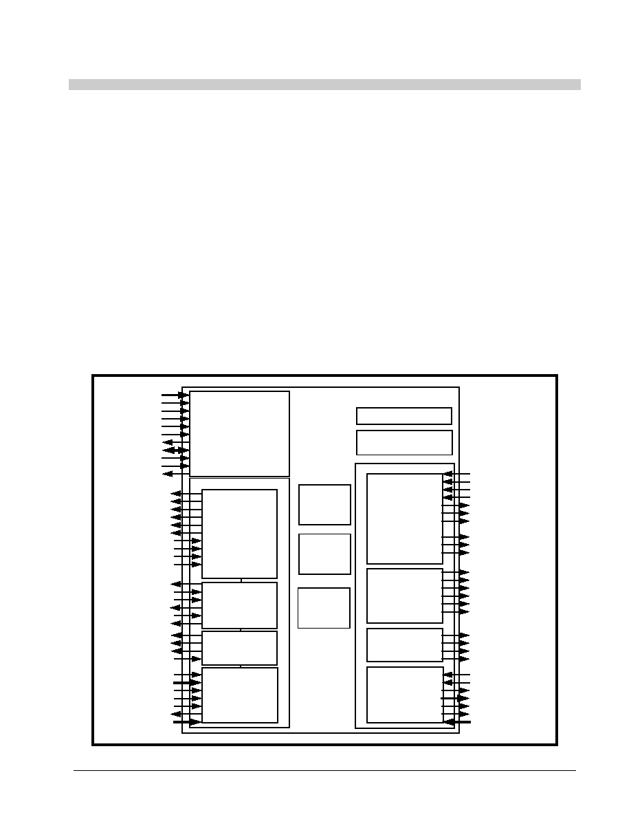
F
IGURE
1. B
LOCK
D
IAGRAM
OF
THE
XRT7245 DS3 UNI IC
Microprocessor Interface
(Programmable
Registers and Interrupt
Block)
Line I/F Drive and Scan
Transmit
DS3
Framer
Transmitter
Receiver
Receive
DS3
Framer
Performance
Monitor
Transmit
PLCP
Processor
Transmit Cell
Processor
Tx Utopia
Interface
Receive
PLCP
Processor
Receive Cell
Processor
Rx Utopia
Interface
A[8:0]
WrB_RW
RdB_DS
CSB*
ALE_AS
Reset
IntB*
D[15:0]
Width16
MOTO/Intel*
Rdy_Dtck
TxPOS
TxNEG
TxFrame
TxOHClk
TxLineClk
TxAISEn
TxFrameRef
TxInClk
TxOHIns
TxOH
TxPFrame
8kRef
StuffCtl
TxPOHFrame
TxPOH
TxPOHClk
TxCellTxed
TxGFCClk
TxGFCMSB
TxGFC
TxClk
TxData[15:0]
TxPrty
TxSoC
TxEnB
RxLineClk
RxNEG
RxPOS
RLOS
RxAIS
RxOHClk
RxOH[7:0]
RxLOS
RxFrame
RxOOF
RxPOHClk
RxPOH
RxPFrame
RxPLOF
RxPOOF
RxPOHFrame
RxCellRxed
RxGFCClk
RxGFCMSB
RxGFC
TxClav/TFullB
RFClk
RxEnB
RxPrty
RxData[15:0]
RxSoC
RxClav/RxEmpty
RxAddr[4:0]
TxAddr[4:0]
Transmit
DS3
Framer
Test and Diagnostic
FEAC
Processor
LAPD
Transceiver
XRT7245
DS3 UNI FOR ATM
·Á
·Á
·Á
·Á
PRELIMINARY
REV. 1.03
2
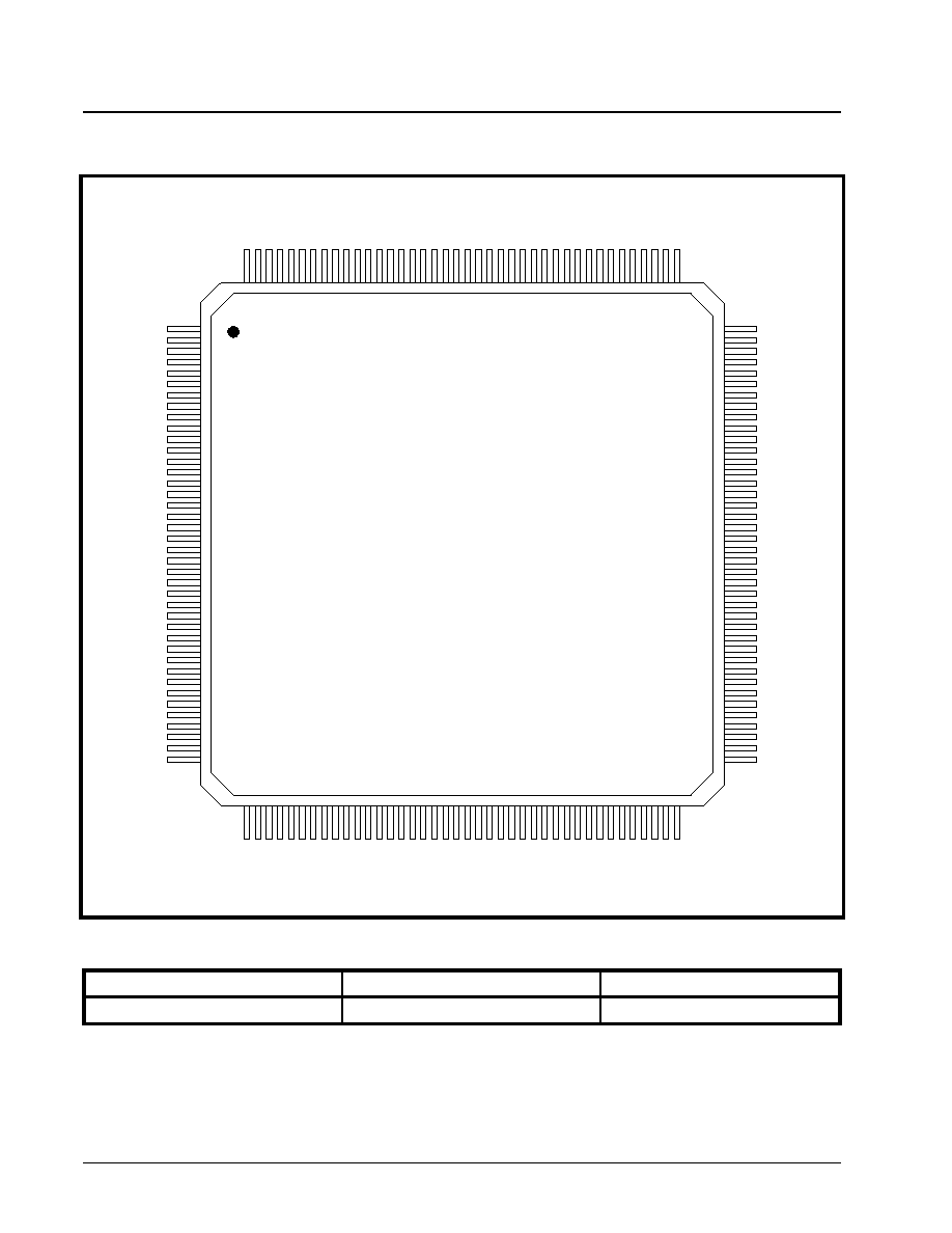
ORDERING INFORMATION
F
IGURE
2. P
IN
O
UT
OF
THE
XRT7245 DS3 UNI
FOR
ATM (160
PIN
QFP)
D 1 5
T A O S
D 1 4
D 1 3
D 1 2
D M O
M O T O / I n t e l
R L O L
D 1 1
T x F r a m e
D 1 0
R E Q B
D 9
D 8
V D D
D 7
D 6
D 5
D 4
W i d t h 1 6
D 3
E n c o D i s
D 2
T x L e v
D 1
R L O O P
D 0
L L O O P
IntB
R x L C D
G N D
C S B
R D _ D S
R x G F C
W R B _ R W
R x P O H
A 8
R x P O H C l k
A 7
R x P O H F r a m e
A6
A5
A4
A3
A2
A1
RxGFCMSB
A0
RxGFClk
RxClk
RxCellRxed
GND
RxData15
RxData7
RxData14
RxData6
RxData13
RxData5
VDD
RxData4
RxData12
RxData3
RxData11
RxData2
RxData10
VDD
RxData9
RxData1
RxData8
RxData0
GND
RxSoC
RxAddr4
RxPrty
RxAddr3
RxClav
RxAddr2
VDD
RxAddr0
RxAddr1
41
42
43
44
45
46
47
48
49
50
51
52
53
54
55
56
57
58
59
60
61
62
63
64
65
66
67
68
69
70
71
72
73
74
75
76
77
78
79
80
X R T 7 2 4 5
Rdy_Dtck
GND
TxGFC
ALE_AS
TxGFCClk
ResetB
TxGFCMSB
GND
GND
TxClk
TxAddr2
TxAddr1
TxAddr3
TxAddr0
TxAddr4
VDD
TxData15
TxData7
TxData14
TxData6
TxData13
TxData5
TxData12
TxData4
VDD
TxData3
TxData11
TxData2
TxData10
TxData1
TxData9
TxData0
TxData8
GND
TxClav
TxPrty
TxSoC
TxEnB
TxOHFrame
TxOHClk
T C e l l T x e d
T x O H
T x P O H C l k
T x O H I n s
T x P O H I n s
T x A I S E n
T x P O H
V D D
T x L i n e C l k
T x N E G
T x P O H F r a m e
T x P O S
T x P F r a m e
T x F r a m e R e f
R x P O O F
G N D
R x P L O F
T x L n C l k
StuffCtl
R x R e d
R x P R e d
R x L i n e C l k
R x N E G
R x P O S
R x F r a m e
R x O H F r a m e
R x P F r a m e
R x O H C l k
R x A I S
G N D
R x O O F
R x O H
R x L O S
EightKRef
R L O S
V D D
N C
G N D
G N D
R x E n B
1 6 0 L e a d P Q F P
160
159
158
157
156
155
154
153
152
151
150
149
148
147
146
145
144
143
142
141
140
139
138
137
136
135
134
133
132
131
130
129
128
127
126
125
124
123
122
121
1
2
3
4
5
6
7
8
9
1 0
1 1
1 2
1 3
1 4
1 5
1 6
1 7
1 8
1 9
2 0
2 1
2 2
2 3
2 4
2 5
2 6
2 7
2 8
2 9
3 0
3 1
3 2
3 3
3 4
3 5
3 6
3 7
3 8
3 9
4 0
1 2 0
1 1 9
1 1 8
1 1 7
1 1 6
1 1 5
1 1 4
1 1 3
1 1 2
1 1 1
1 1 0
1 0 9
1 0 8
1 0 7
1 0 6
1 0 5
1 0 4
1 0 3
1 0 2
1 0 1
1 0 0
9 9
9 8
9 7
9 6
9 5
9 4
9 3
9 2
9 1
9 0
8 9
8 8
8 7
8 6
8 5
8 4
8 3
8 2
8 1
P
ART
N
UMBER
P
ACKAGE
O
PERATING
T
EMPERATURE
R
ANGE
XRT7245SIQ160
28 x28 mm Plastic QFP
-40∞C to +85∞C

·Á
·Á
·Á
·Á
DS3 UNI FOR ATM
XRT7245
PRELIMINARY
REV. 1.03
3
FUNCTIONAL DESCRIPTION
The XRT7245 UNI can functionally be subdivided in-
to 6 different sections, as shown in Figure 1.
∑
Receive Section
∑
Transmit Section
∑
Microprocessor Interface Section
∑
Performance Monitor Section
∑
Test and Diagnostic Section
∑
Line Interface Unit Scan Drive Section
The features of each of these functional sections are
briefly outlined below.
THE RECEIVE SECTION
The purpose of the Receiver Section of the XRT7245
DS3 ATM UNI device is to allow a local ATM Layer (or
ATM Adaptation Layer) processor to receive ATM cell
data from a remote piece of equipment via a public or
leased DS3 transport medium.
The Receive Section of the XRT7245 DS3 UNI con-
sists of the following functional blocks.
∑
Receive DS3 Framer Block
∑
Receive PLCP (Physical Layer Convergence Proto-
col) Processor Block
∑
Receive Cell Processor Block
∑ Receive UTOPIA Interface Block
The Receive Section of the UNI device will:
∑ The Receive DS3 Framer will synchronize to the
incoming DS3 data stream and remove or process
the DS3 Framing/Overhead Bits. This procedure
will result in either extracting PLCP frame data or
"Direct-Mapped" ATM Cell data, from the payload
portion of the incoming DS3 data stream. The
Receive DS3 Framer can used to receive FEAC
(Far End Alarm & Control) messages via an on-
chip FEAC Transceiver.
Additionally, the Receive DS3 Framer includes an on-
chip LAPD Receiver that can receive incoming path
maintenance data link messages from the far-end
Transmit DS3 Framer of the "Far End" Terminal.
Note: The Receive DS3 Framer supports both M13 and C-
bit Parity Frame Formats.
∑
The Receive PLCP Processor will identify the
frame boundary of each incoming PLCP frame,
extract and process the overhead bytes of these
PLCP frames (applies only if the UNI is operating in
the PLCP Mode). The Receive PLCP Processor
will also perform some error checking on the
incoming PLCP frames. The Receive PLCP Pro-
cessor will inform the Far-End (Transmitting UNI) of
the results of this error-checking by internally rout-
ing these results to the "Near-End" Transmit PLCP
Processor, for transmission back out to the Far-End
Terminal.
∑
The Receive Cell Processor will perform the follow-
ing functions:
≠ Cell Delineation
≠ HEC Byte Verification of incoming cells
(optional)
≠ Cell-payload de-scrambling (optional)
≠ Idle cell detection and removal (optional)
≠ User and OAM Cell Filtering (optional)
≠ OAM Cell Processing (optional)
∑
The UNI provides 54 bytes of on-chip RAM that
allows for the reception and processing of selected
OAM cells.
∑ The RxFIFO, within the Receive UTOPIA Interface
block will temporarily hold any ATM cells that pass
through the Receive Cell Processor, where they can
be read out by the ATM Layer processor, over the
Receive UTOPIA Data Bus.
THE TRANSMIT SECTION
The purpose of the Transmit section of the XRT7245
DS3 ATM UNI device is to allow a local ATM Layer (or
ATM Adaptation Layer) processor to transmit ATM
Cell data to a remote piece of equipment via a public
or leased DS3 transport medium.
The Transmit Section of the XRT7245 DS3 UNI con-
sists of the following functional blocks.
∑
Transmit UTOPIA Interface Block
∑
Transmit Cell Processor Block
∑
Transmit PLCP Processor Block
∑ Transmit DS3 Framer Block
The Transmit Section of the UNI device will:
∑
Allow the ATM Layer processor to write ATM cells
into the Transmit FIFO (within the Transmit UTOPIA
Interface block) via a standard UTOPIA Level 2
interface.
∑
The Transmit Cell Processor will read in these cells
from the Transmit FIFO (if available) for further
processing. If no cell is available within the Trans-
mit FIFO, then the Transmit Cell Processor will
automatically generate an Idle cell. The UNI is
equipped with on-chip registers to allow for the
generation of customized Idle cells.

XRT7245
DS3 UNI FOR ATM
·Á
·Á
·Á
·Á
PRELIMINARY
REV. 1.03
4
∑
The UNI provides 54 bytes of on-chip RAM that
allows for the generation and transmission of "user-
specified" OAM cells. The Transmit Cell Processor
will generate and transmit these OAM cells upon
software command.
∑
The Transmit Cell Processor will (optionally) scramble
the Cell Payload bytes and (optionally) compute
and insert the HEC (Header Error Check) byte.
This HEC byte will be inserted into the fifth octet of
each cell prior to being transferred to the Transmit
PLCP Processor (or the Transmit DS3 Framer).
∑
The Transmit PLCP Processor will pack 12 ATM cells
into each PLCP frame and automatically determine
the nibble-stuffing option of the current PLCP frame.
These PLCP frames will also include an overhead
byte that reflect BIP-8 (Bit Interleaved Parity) calcu-
lation results, a byte that reflects the current stuffing
option status of the current PLCP frame, Path
Overhead and Identifier bytes, and diagnostic-
related bytes reflecting any detected BIP-8 errors
and alarm conditions detected in the Receive section
of the UNI chip.
∑ These PLCP frames (or "Direct Mapped" ATM
cells) will be inserted into the payload of an outgo-
ing DS3 frame, for transmission to the "Far-End" Ter-
minal, by the Transmit DS3 Framer. The Transmit
DS3 Framer will transmit FEAC (Far End Alarm &
Control) messages to the Far-End Receiver via an
on-chip FEAC Transceiver.Additionally, the Trans-
mit DS3 Framer can transmit path maintenance
data link messages to the Far-End Terminal via the
on-chip LAPD Transmitter.
Note: The Transmit DS3 Framer will support either M13 or
C-bit Parity Framing Formats.
THE MICROPROCESSOR INTERFACE SECTION
The Microprocessor Interface Section allows a user (or
a local "housekeeping" processor) to do the following:
∑
To configure the UNI IC into a wide variety of oper-
ating modes; by writing data into any one of a large
number of "read/write" registers.
∑
To monitor many aspects of the UNI's performance
by reading data from any one of a large number of
"read/write" and "read-only" registers.
∑
To run in a "polling" or "interrupt-driven" environment.
The UNI IC contains an extensive interrupt structure
consisting of a wide range of interrupt enable and
interrupt status registers.
∑
To command the UNI IC to transmit OAM cells,
FEAC messages and/or LAPD Messages frames,
upon software command.
∑
To read in and process received OAM cells, FEAC
messages and/or Path Maintenance Data Link
Messages from the UNI IC.
∑
The Microprocessor Interface allows the user to
interface the XRT7245 DS3 UNI to either an Intel
type or Motorola type processor. Additionally, the
Microprocessor Interface can be configured to
operate over an 8-bit or 16-bit data bus.
∑ The Microprocessor Interface section includes a
"Loss of Clock Signal" protection feature that auto-
matically completes (or terminates) a "Read/Write"
operation, should a "Loss of Clock Signal" event
occur.
PERFORMANCE MONITOR SECTION
The Performance Monitor Section of the XRT7245
DS3 UNI consists of a large number of "Reset-upon-
Read" and "Read-Only" registers that contains cumu-
lative and "one-second" statistics that reflect the per-
formance/health of the UNI chip/system. These cu-
mulative and "one-second" statistics are kept on
some of the following parameters.
∑
Number of Line Code Violation events detected by
the Receive DS3 Framer
∑
Number of Framing Bit (F- and M-bit) errors
detected by the Receive DS3 Framer
∑
Number of P-bit Errors detected by the Receive
DS3 Framer
∑
Number of FEBE Events detected by the Receive
DS3 Framer
∑
Cumulative number of BIP-8 errors, detected by
the Receive PLCP Processor
∑
Number of PLCP framing errors, detected by the
Receive PLCP Processor
∑
Cumulative sum of the FEBE value, in the incoming
G1 bytes (within each PLCP frame), received by
the Receive PLCP Processor
∑
Number of Single-bit HEC byte Errors detected
∑
Number of Multi-bit HEC byte Errors detected
∑
Number of Received Idle Cells
∑
Number of Received Valid (User and OAM) cells
discarded
∑
Number of Discarded Cells
∑
Number of Transmitted Idle Cells
∑ Number of Transmitted Valid Cells
TEST AND DIAGNOSTIC SECTION
The Test and Diagnostic Section allows the user to
perform a series of tests in order to verify proper
functionality of the UNI chip and/or the user's system.

·Á
·Á
·Á
·Á
DS3 UNI FOR ATM
XRT7245
PRELIMINARY
REV. 1.03
5
The "Test and Diagnostic" section provides the UNI
IC with the following capabilities.
∑
Allows the UNI to operate in the Line, Cell, and
PLCP Loop-back Modes
∑
Contains an internal Test Cell Generator and an
internal Test Cell Receiver. The Test Cell Generator
will generate Test Cells with "user-defined" header
byte patterns. The Test Cell Generator will also fill
the payload portion of these test cells with bytes
from an on-chip PRBS generator.
∑
The Test Cell Generator can generate test cells in
"One Shot" Mode (e.g., a burst of 1024 test cells) or in
"Continuous" Mode (e.g., a continuous stream of
test cells).
∑ The Test Cell Receiver will identify and collect the
Test Cells for further analyses, based upon the
"user-defined" header byte patterns. Additionally,
the Test Cell Receiver will report the occurrence of
any errors by incrementing an on-chip register.
LINE INTERFACE DRIVE AND SCAN SECTION
The Line Interface Drive and Scan Section allows the
user to monitor and control many aspects of the
XRT7295 DS3 Line Receiver IC and the XRT7296
DS3 Line Transmitter IC, via on-chip registers, within
the UNI IC. This feature eliminates the need for glue
logic to interface the XRT7245 DS3 UNI to the
XRT7295/XRT7296 DS3 Line Interface Unit ICs.
∑ The On-Chip Line Interface Drive register allows
the user to control the state of 6 output pins. The
function of these output pins, when asserted, are
tabulated below.
Signal Name
Function of Output Pin
REQB
Receive Equalizer By-Pass:
Setting this bit-field to "1" configures the XRT7300 device to shut off its internal Receive Equalizer.
Setting this bit-field to "0" configures the XRT7300 device to enable its internal Receive Equalizer.
TAOS
Transmit "All Ones" Pattern.
Setting this bit-field to "1" configures the XRT7300 LIU IC to overwrite the DS3 data that is output via
the TxPOS and TxNEG outputs, and transmit an "All Ones" pattern onto the line.
Setting this bit-field to "0" configures the XRT7300 LIU IC to transmit data, as is applied to it via the
TPDATA and TNDATA input pins.
ENCODIS
B3ZS Encoder Disable/Enable Select.
Setting this bit-field to "1" disables the B3ZS Encoder, within the XRT7300 device.
Setting this bit-field to "0" enables the B3ZS Decoder within the XRT7300 device.
TxLev
Transmit Output Signal Line Build Out Select.
Setting this bit-field to "1" disables the Transmit Line Build Out circuitry within the XRT7300 device. In
this case, the XRT7300 will generate an "unshaped" square wave signal out onto the line (via the TTIP
and TRING output pins).
Note: In order to configure the XRT7300 device to generate a line signal that complies with the Transmit
Output Pulse Template Requirements (per GR-499-CORE), this setting is advised if the cable length
between the Transmit Output of the XRT7300 device and the Cross-Connect is greater than 225 feet.
Setting this bit-field to "0" enables the Transmit Line Build Out circuitry within the XRT7300 device. In
this case, the XRT7300 device will generate a "shaped" square wave out onto the line (via the TTIP and
TRING output pins).
Note: In order to configure the XRT7300 device to generate a line signal that complies with the Transmit
Output Pulse Template Requirements (per GR-499-CORE), this setting is advised if the cable length
between the Transmit Output of the XRT7300 device and the Cross-Connect is less than 225 feet.

XRT7245
DS3 UNI FOR ATM
·Á
·Á
·Á
·Á
PRELIMINARY
REV. 1.03
6
∑
The On-Chip Line Interface Scan Register allows
the user to monitor the state of 3 input pins. The
function of these input pins, when asserted, are
tabulated below.
FEATURES
TRANSMIT AND RECEIVE SECTIONS
UTOPIA I
NTERFACE
B
LOCKS
∑
Compliant with UTOPIA Level 2 Interface Specifi-
cation (e.g., supports Single-PHY or Multi-PHY
operation).
∑
8-bit or 16-bit wide UTOPIA Data Bus operation in
the Transmit and Receive Directions.
∑
The UTOPIA Data Bus runs at clock rates of 25
MHz, 33 MHz and 50 MHz
∑
Supports Octet-Level and Cell-Level Handshaking
between the UNI and the ATM Layer processor.
∑
The Transmit UTOPIA Interface block performs par-
ity checking of ATM cell data that is written into it,
by the ATM Layer processor. Will optionally discard
errored cells.
∑
Contains on-chip 16 cell FIFO in the Transmit
Direction (TxFIFO)
∑
The TxFIFO can be configured to operate with
depths of 4, 8, 12 or 16 cells
∑ Contains on-chip 4 cell FIFO in the Receive
Direction (RxFIFO)
RLOOP
Remote Loop-Back Mode Select:
This bit-field, along with LLOOP can be used to configure the XRT7300 device into one of four different
loop-back modes.
Setting RLOOP to "1" (with LLOOP = 0) configures the XRT7300 device to operate in the Remote
Loop-Back Mode.
Setting RLOOP to "1" (with LLOOP = 1) configures the XRT7300 device to operate in the "Digital Local
Loop-Back" Mode.
Setting RLOOP to "0" (with LLOOP = 1) configures the XRT7300 device to operate in the "Analog Local
Loop-Back" Mode.
Setting RLOOP to "0" (with LLOOP = 0) configures the XRT7300 device to operate in the "Normal"
(No-Loop-back) Mode.
LLOOP
Local Loop-Back Mode Select:
This bit-field along with RLOOP can be used to configure the XRT7300 device into one of four different
loop-back modes.
Setting LLOOP to "1" (with RLOOP = 0) configures the XRT7300 device to operate in the "Analog Local
Loop-back" Mode.
Setting LLOOP to "1" (with RLOOP = 1) configures the XRT7300 device to operate in the "Digital Local
Loop-back" Mode.
Setting LLOOP to "0" (with RLOOP = 0) configures the XRT7300 device to operate in the "Normal"
(No-Loop-back) Mode.
Setting LLOOP to "0" (with RLOOP = 1) configures the XRT7300 device to operate in the "Remote
Loop-back" Mode.
Signal Name
Function of Output Pin
S
IGNAL
N
AME
F
UNCTION
OF
I
NPUT
P
IN
IF
ASSERTED
DMO
Indicates that the "Drive Monitor" circuitry within the XRT7300 has not detected any bipolar signals
within the last 128 ± 32 bit periods.
RLOL
Indicates that the "Clock Recovery" circuit, within the XRT7300 has lost "lock" with the incoming DS3
line signal.
RLOS
Indicates that the XRT7300 device is declaring an LOS (Loss of Signal) Condition.

·Á
·Á
·Á
·Á
DS3 UNI FOR ATM
XRT7245
PRELIMINARY
REV. 1.03
7
T
RANSMIT
C
ELL
P
ROCESSOR
B
LOCK
∑
Optionally computes and inserts HEC byte into all
cells (user, OAM and Idle).
∑
Optionally scrambles the payload of each cell.
∑
Idle cells are automatically generated when no
user cells are available in the TxFIFO.
∑
UNI contains on-chip registers that support the
generation/transmission of default or custom Idle
cells.
∑
UNI contains the on-chip "Transmit OAM Cell" buffer
(54 bytes) that allows the user to write in and store
the contents of OAM cells, in preparation for trans-
mission.
∑
OAM cells are transmitted upon software command.
∑
Performs "Data Path Integrity" check on all incoming
cell data, originating from the ATM Layer processor.
∑ Provides a serial input port to allow the user to
insert the GFC (Generic Flow Control) field exter-
nally into the GFC nibble field of an outbound (e.g.,
Transmit direction) valid ATM Cell.
R
ECEIVE
C
ELL
P
ROCESSOR
B
LOCK
∑
Performs cell delineation on either "Direct Mapped"
ATM cell data or PLCP frames.
∑
Verifies the HEC bytes of incoming cells and cor-
rects most cells with single bit errors. Cells with
multi-bit errors are detected and are optionally dis-
carded.
∑
(Optionally) Performs filtering of Idle Cells.
∑
(Optionally) Performs filtering of User and OAM cells.
∑
UNI contains on-chip buffer space ("Receive OAM
Cell" buffer) that allows for the reception and pro-
cessing of selected OAM cells.
∑
Optionally de-scrambles the payload of each cell.
∑
Provides a serial output port that allows the user to
read the GFC value of an incoming (e.g., Receive
direction) ATM Cell.
∑ Inserts the "Data Path Integrity Check" patterns in
all cells that are written to the RxFIFO.
T
RANSMIT
PLCP P
ROCESSOR
B
LOCK
∑
Can be disabled to support the "Direct Mapped"
ATM mode.
∑
Packs 12 ATM cells into each PLCP frame along
with various other overhead bytes.
∑
The Transmit PLCP Processor will automatically
determine its own stuffing options.
∑
Overhead bytes include those that support BIP-8
calculations (B1), indicator of stuff-option status for
current PLCP frame (C1), diagnostic byte that
reflects alarms conditions that were detected in the
Receive Section of the UNI (G1); and Path Over-
head bytes.
∑ Provides a serial input port for user to insert PLCP
Overhead Bytes externally.
R
ECEIVE
PLCP P
ROCESSOR
B
LOCK
∑
Can be disabled to support the "Direct Mapped"
ATM mode.
∑
Determines the frame boundaries of incoming
PLCP frames (from the Receive DS3 Framer).
∑
Extracts and processes the PLCP frame overhead
bytes.
∑
Provides a serial output port for user to read in the
contents of the PLCP Overhead Bytes from the
incoming data.
T
RANSMIT
/R
ECEIVE
DS3 F
RAMER
B
LOCK
∑
Supports the M13 and C-bit Parity Framing Formats.
∑
Transmit and Receive DS3 Framers can transmit/
receive data in the Unipolar or the Bipolar (AMI or
B3ZS line codes) format.
∑
The Transmit DS3 Framer provides a serial input
port that allows the user to insert his/her own
values for the overhead bits of the "outbound"
DS3 frames.
∑
The Receive DS3 Framer provides a serial output
port that allows the user access to the values of the
overhead bits of the "incoming" DS3 frames.
∑
The Receive DS3 Framer can be configured to
sample the incoming DS3 data (at the RxPOS and
RxNEG input pins) via the rising edge or falling
edge of the Receive Line Clock (RxLineClk) input.
∑
The Transmit DS3 Framer can be configured to
update the "outbound" DS3 data (at the TxPOS and
TxNEG output pins) at the rising edge or falling
edge of the Transmit Line Clock (TxLineClk) output.
∑
UNI includes on-chip RAM space to support the
transmission and reception of path maintenance data
link messages via an on-chip LAPD Transceiver
∑
UNI includes on-chip registers to support the trans-
mission and reception of FEAC (Far End Alarm &
Control) messages via an on-chip FEAC Transceiver.
∑
Contains on-chip FEAC Transceiver.
∑ Contains on-chip LAPD Transceiver.
M
ICROPROCESSOR
I
NTERFACE
S
ECTION
∑
Can be interfaced to Motorola or Intel type of
microprocessors/microcontrollers

XRT7245
DS3 UNI FOR ATM
·Á
·Á
·Á
·Á
PRELIMINARY
REV. 1.03
8
∑
Microprocessor interface supports 8 bit wide or 16-
bit wide read/write accesses.
∑
Supports polled or interrupt-driven environments.
∑
Supports burst mode "Read and Write" operations
between the "local" microprocessor and the UNI on-
chip registers and RAM locations.
∑ Includes a "Loss of Clock Signal" protection feature
that terminates "Read/Write" cycles with the local
µ
P, during a "Loss of Clock signal" event.
P
ERFORMANCE
M
ONITOR
S
ECTION
Contains numerous on-chip "Read-Only" registers
that allows the user to monitor the overall "health" of
the system.
T
EST
AND
D
IAGNOSTIC
S
ECTION
∑
Supports Line, PLCP, and Cell Loop-back Modes
∑
Supports Line-Side Testing
∑
Contains an on-chip Test Cell Generator and an
on-chip Test Cell Receiver
∑
Test Cell Generator can generate a "continuous"
stream of test cells, or a "one-shot" burst of 1024
test cells.
∑
The Test Cell Receiver identifies, collects and eval-
uates Test Cells for errors.
∑ The Test Cell Receiver also reports the occurrence
of errors to the user.
L
INE
I
NTERFACE
D
RIVE
AND
S
CAN
S
ECTION
∑
Consists of an on-chip "Read/Write" register that
allows the user to control the state of 6 output pins.
∑ Consists of an on-chip "Read-Only" register that
allows the user to monitor the state of 3 input pins.

·Á
·Á
·Á
·Á
DS3 UNI FOR ATM
XRT7245
PRELIMINARY
REV. 1.03
9
)Pin Descriptions (see Figure 2)
PIN DESCRIPTION
P
IN
N
O
. S
YMBOL
T
YPE
D
ESCRIPTION
1
D15
I/O
MSB of Bi-Directional Data Bus (Microprocessor Interface Section): This pin,
along with pins D0 - D14, function as the Microprocessor Interface bi-directional data
bus, and is intended to be interfaced to the "local" microprocessor. This pin is inactive
if the Microprocessor Interface block is configured to operate over an 8 bit data bus.
2
TAOS
O
"Transmit All Ones Signal" (TAOS) Command (for the XR-T7296 DS3 Line
Transmitter IC).
This output pin is intended to be connected to the TAOS input pin of the XR-T7296
DS3 Line Transmitter IC. The user can control the state of this output pin by writing a
`0' or `1' to Bit 4 (TAOS) of the Line Interface Drive Register (Address = 72h). If the
user commands this signal to toggle "high" then it will force the XR-T7296 DS3 Line
Transmitter IC to transmit an "All Ones" pattern onto the line. Conversely, if the user
commands this output signal to toggle "low" then the XR-T7296 DS3 Line Transmitter
IC will proceed to transmit data based upon the pattern that it receives via the TxPOS
and TxNEG output pins.
Writing a "1" to Bit 4 of the Line Interface Drive Register (Address = 72h) will cause this
output pin to toggle "high". Writing a "0" to this bit-field will cause this output pin to toggle
"low".
Note: If the customer is not using the XR-T7296 DS3 Line Transmitter IC, then he/she
can use this output pin for a variety of other purposes.
3
D14
I/O
Bi-directional Data bus (Microprocessor Interface Section): This pin is inactive if
the Microprocessor Interface block is configured to operate over an 8 bit data bus.
(Please see description for D15)
4
D13
I/O
Bi-directional Data bus (Microprocessor Interface Section): This pin is inactive if
the Microprocessor Interface block is configured to operate over an 8 bit data bus.
(Please see description for D15)
5
D12
I/O
Bi-directional Data bus (Microprocessor Interface Section): This pin is inactive if
the Microprocessor Interface block is configured to operate over an 8 bit data bus.
(Please see description for D15)
6 DMO
I
"Drive Monitor Output" Input (from the XRT7300 LIU IC).
This input pin is intended to be tied to the DMO output pin of the XRT7300 DS3/E3
LIU IC. The user can determine the state of this input pin by reading Bit 2 (DMO)
within the Line Interface Scan Register (Address = 73h). If this input signal is "high",
then it means that the drive monitor circuitry (within the XRT7300 LIU IC) has not
detected any bipolar signals at the MTIP and MRING inputs within the last 128 ± 32
bit-periods. If this input signal is "low", then it means that bipolar signals are being
detected at the MTIP and MRING input pins of the XRT7300 device.
Note: If this customer is not using the XRT7300 DS3 LIU IC, then he/she can use this
input pin for a variety of other purposes.
7
MOTO
I
Motorola/Intel Processor Interface Select Mode: This input pin allows the user to
configure the Microprocessor Interface to interface with either a "Motorola-type" or
"Intel-type" microprocessor/microcontroller. Tying this input pin to VCC, configures the
microprocessor interface to operate in the Motorola mode (e.g., the UNI device can be
readily interfaced to a "Motorola type" local microprocessor). Tying this input pin to
GND configures the microprocessor interface to operate in the Intel Mode (e.g., the
UNI device can be readily interfaced to an "Intel type" local microprocessor).

XRT7245
DS3 UNI FOR ATM
·Á
·Á
·Á
·Á
PRELIMINARY
REV. 1.03
10
8
RLOL
I
Receive Loss of Lock Indicator--from the XRT7300 DS3/E3 LIU IC.
This input pin is intended to be connected to the RLOL (Receive Loss of Lock) output
pin of the XRT7300 LIU IC. The user can monitor the state of this pin by reading the
state of Bit 1 (RLOL) within the Line Interface Scan Register (Address = 73h). If this
input pin is "low", then it means that the phase-locked-loop circuitry, within the XRT7300
device is properly locked onto the incoming DS3 data-stream; and is properly recover-
ing clock and data from this DS3 data-stream. However, if this input pin is "high", then
it means that the phase-locked-loop circuitry, within the XRT7300 device has lost lock
with the incoming DS3 data-stream, and is not properly recovering clock and data.
For more information on the operation of the XRT7300 DS3/E3/STS-1 LIU IC, please
consult the "XRT7300 DS3/E3/STS-1 LIU IC" data sheet.
Note: If the customer is not using the XRT7300 LIU IC, he/she can use this input pin
for other purposes.
9
D11
I/O
Bi-Directional Data bus (Microprocessor Interface Section):
10
TxFrame
O
Transmit End of DS3 Frame Indicator: This output pin indicates that the last bit of an
outbound DS3 frame is being transmitted from the TxPOS and TxNEG output pins.
This pin marks the end of DS3 frame by pulsing "high" for one bit period at the end of each
frame.
11
D10
I/O
Bi-Directional Data bus (Microprocessor Interface Section): This pin is inactive if
the Microprocessor Interface block is configured to operate over an 8 bit data bus.
(Please see description for D15)
12
REQB
O
Receive Equalization Bypass Control Output Pin--(to be connected to the
XRT7300 DS3/E3 LIU IC):
This output pin is intended to be connected to the REQB input pin of the XRT7300 DS3/
E3 LIU IC. The user can control the state of this output pin by writing a `0' or `1' to Bit 5
(REQB) of the Line Interface Driver Register (Address = 72h). If the user commands
this signal to toggle "high" then it will cause the incoming DS3 line signal to "by-pass"
equalization circuitry, within the XRT7300 Device. Conversely, if the user commands
this output signal to toggle "low", then the incoming DS3 line signal with be routed
through the equalization circuitry. For information on the criteria that should be used
when deciding whether to bypass the equalization circuitry or not, please consult the
"XRT7300 DS3/E3/STS-1 LIU IC" data sheet.
Writing a "1" to Bit 5 of the Line Interface Drive Register (Address = 72h) will cause this
output pin to toggle "high". Writing a "0" to this bit-field will cause this output pin to toggle
"low".
Note: If the customer is not using the XRT7300 DS3/E3/STS-1 LIU IC, then he/she
can use this output pin for a variety of other purposes.
13
D9
I/O
Bi-Directional Data bus (Microprocessor Interface Section): This pin is inactive if
the Microprocessor Interface block is configured to operate over an 8 bit data bus.
(Please see description for D15)
14
D8
I/O
Bi-Directional Data bus (Microprocessor Interface Section): This pin is inactive if
the Microprocessor Interface block is configured to operate over an 8 bit data bus.
(Please see description for D15)
15
VDD
***
Power Supply Pin
PIN DESCRIPTION (CONT'D)
P
IN
N
O
. S
YMBOL
T
YPE
D
ESCRIPTION

·Á
·Á
·Á
·Á
DS3 UNI FOR ATM
XRT7245
PRELIMINARY
REV. 1.03
11
16
D7
I/O
Bi-Directional Data bus (Microprocessor Interface Section): (Please see descrip-
tion for D15)
17
D6
I/O
Bi-Directional Data bus (Microprocessor Interface Section): (Please see descrip-
tion for D15)
18
D5
I/O
Bi-Directional Data bus (Microprocessor Interface Section): (Please see descrip-
tion for D15)
19
D4
I/O
Bi-Directional Data bus (Microprocessor Interface Section): (Please see descrip-
tion for D15)
20
Width16
I
Microprocessor Interface Block Data Bus Width Selector: This input pin allows the
user to configure the microprocessor interface of the UNI, to operate over either an 8
or 16 bit wide data bus. Tying this pin to VCC configures the Microprocessor Interface
Data Bus width to be 16 bits. Tying this pin to GND configures the Microprocessor
Interface Data Bus width to be 8 bits.
21
D3
I/O
Bi-Directional Data bus (Microprocessor Interface Section): (Please see descrip-
tion for D15)
22
Encodis
O
Encoder (B3ZS) Disable Output pin (intended to be connected to the XRT7300
DS3/E3 LIU IC).
This output pin is intended to be connected to the Encodis input pin of the XRT7300
LIU IC. The user can control the state of this output pin by writing a "0" or "1" to Bit 3
(Encodis) of the Line Interface Driver Register (Address = 72h). If the user commands
this signal to toggle "high" then it will disable the B3ZS encoder circuitry within the
XRT7300 IC. Conversely, if the user commands this output signal to toggle "low", then
the B3ZS Encoder circuitry, within the XRT7300 IC will be enabled.
Writing a "1" to Bit 3 of the Line Interface Driver Register (Address = 72h) will cause this
output pin to toggle "high". Writing a "0" to this bit-field will cause this output pin to toggle
"low".
Notes:
1. The user is advised to disable the B3ZS encoder (within the XRT7300 IC) if the
Transmit and Receive DS3 Framers (within the UNI) are configured to operate
in the B3ZS line code.
2. If the customer is not using the XRT7300 DS3 Line Transmitter IC, then he/
she can use this output pin for a variety of other purposes.
23
D2
I/O
Bi-Directional Data bus (Microprocessor Interface Section): (Please see descrip-
tion for D15)
PIN DESCRIPTION (CONT'D)
P
IN
N
O
. S
YMBOL
T
YPE
D
ESCRIPTION

XRT7245
DS3 UNI FOR ATM
·Á
·Á
·Á
·Á
PRELIMINARY
REV. 1.03
12
24
TxLev
O
Transmit Line Build Enable/Disable Select (to be connected to the TxLev input
pin of the XRT7300 DS3/E3 LIU IC).
This output pin is intended to be connected to the TxLev input pin of the XRT7300 DS3/
E3 LIU IC. The user can control the state of this output pin by writing a "0" or a "1" to Bit
2 (TxLev) within the Line Interface Driver Register (Address = 72h).
If the user commands this signal to toggle "high" then it will disable the "Transmit Line
Build-Out" circuitry within the XRT7300 device. In this case, the XRT7300 device will
output unshaped (square-wave) pulses onto the "Transmit Line Signal". In order to
insure that the XRT7300 device generates a line signal that is compliant with the
Bellcore GR-499-CORE Pulse Template requirements (at the Cross-Connect), the
user is advised to set this output pin high, if the cable length (between the Transmit
Output of the XRT7300 device and the Cross-Connect) is greater than 225 feet.
Conversely, if the user commands this signal to toggle "high", then it will enable the
"Transmit Line Build-Out" circuitry within the XRT7300 device. In this case, the
XRT7300 device will output shaped pulses onto the "Transmit Line Signal". In order to
ensure that the XRT7300 device generates a line signal that is compliant with the
Bellcore GR-499-CORE Pulse Template requirements (at the Cross-Connect), the
user is advised to set this output pin low, if the cable length (between the Transmit
Output of the XRT7300 device and the Cross Connect) is less than 225 ft. of cable.
Writing a "1" to Bit 2 of the Line Interface Drive Register (Address = 72h) will cause this
output pin to toggle "high". Writing a "0" to this bit-field will cause this output pin to toggle
"low".
Note: If the customer is not using the XRT7300 DS3/E3 LIU IC, then he/she can use
this output pin for a variety of other purposes.
25
D1
I/O
Bi-Directional Data bus (Microprocessor Interface Section): (Please see descrip-
tion for D15)
26
RLOOP
O
Remote Loop-back Output Pin (to the XRT7300 DS3/E3 LIU IC).
This output pin is intended to be connected to the RLOOP input pin of the XRT7300 LIU
IC. The user can command this signal to toggle "high" and, in turn, force the XRT7300
into the "Remote Loop-back" mode. Conversely, the user can command this signal to
toggle "low" and allow the XRT7300 device to operate in the normal mode. (For a
detailed description of the XRT7300 LIU IC's operation during Remote Loop-back,
please see the XRT7300 DS3/E3/STS-1 LIU IC Data Sheet).
Writing a "1" to bit 1 of the "Line Interface Drive Register (Address = 72h) will cause
this output pin to toggle "high". Writing a "0" to this bit-field will cause the RLOOP out-
put to toggle "low".
Note: If the customer is not using the XRT7300 DS3/E3/STS-1 IC, then he/she can
use this output pin for a variety of other purposes.
27
D0
I/O
Bi-Directional Data bus (Microprocessor Interface Section): (Please see descrip-
tion for D15)
PIN DESCRIPTION (CONT'D)
P
IN
N
O
. S
YMBOL
T
YPE
D
ESCRIPTION

·Á
·Á
·Á
·Á
DS3 UNI FOR ATM
XRT7245
PRELIMINARY
REV. 1.03
13
28
LLOOP
O
Local Loop-back Output Pin (to the XRT7300 DS3/E3/STS-1 LIU IC).
This output pin is intended to be connected to the LLOOP input pin of the XRT7300
LIU IC. The user can command this signal to toggle "high" and, in turn, force the LIU
into the "Local Loop-back" mode. (For a detailed description of the XRT7300 LIU IC's
operation during Local Loop-back, please see the XRT7300 DS3/E3/STS-1 LIU IC
Data Sheet).
Writing a "1" to bit 1 of the "Line Interface Drive Register" (Address = 72h) will cause
this output pin to toggle "high". Writing a "0" to this bit-field will cause the RLOOP out-
put to toggle "low".
Note: If the user is not using the XRT7300 DS3/E3/STS-1 LIU IC, then he/she can
use this output pin for a variety of other purposes.
29
IntB*
O
Interrupt Request Output: This open-drain, active-low output signal will be asserted
when the UNI device is requesting interrupt service from the local microprocessor. This
output pin should typically be connected to the "Interrupt Request" input of the local
microprocessor.
30
RxLCD
O
Loss of Cell Delineation Indicator: This active-high output pin will be asserted
whenever the Receive Cell Processor has experienced a "Loss of Cell Delineation".
This pin will return "low" once the Receive Cell Processor has regained Cell Delinea-
tion.
31
GND
***
Ground Pin Signal
32
CSB*
I
Chip Select Input: This active-low input signal selects the Microprocessor Interface
Section of the UNI device and enables Read/Write operations between the "local"
microprocessor and the UNI on-chip registers and RAM locations.
33
RDB_DS
I
Read Data Strobe (Intel Mode): If the microprocessor interface is operating in the
Intel Mode, then this input will function as the RD* (READ STROBE) input signal from
the local
µ
P
. Once this active low signal is asserted, then the UNI will place the con-
tents of the addressed registers (within the UNI) on the Microprocessor Data Bus
(D[15:0]). When this signal is negated, the Data Bus will be tri-stated.
Data Strobe (Motorola Mode): If the microprocessor interface is operating in the
Motorola mode, then this pin will function as the active low Data Strobe signal.
34
RxGFC
O
Receive GFC Nibble Field Serial Output pin: This pin, along with the RxGFCClk
and the RxGFCMSB pins form the "Receive GFC Nibble-Field" serial output port. This
pin will serially output the contents of the GFC Nibble field of each cell that is pro-
cessed through the Receive Cell Processor. This data is serially clocked out of this pin
on the rising edge of the RxGFCClk signal. The Most Significant Bit (MSB) of each
GFC value is designated by a pulse at the RxGFCMSB output pin.
35
WRB_RW
I
Write Data Strobe (Intel Mode): If the microprocessor interface is operating in the
Intel Mode, then this active low input pin functions as the WR* (Write Strobe) input sig-
nal from the
µ
P. Once this active-low signal is asserted, then the UNI will latch the
contents of the
µ
P Data Bus, into the addressed register (or RAM location) within the
UNI IC.
R/W Input Pin (Motorola Mode): When the Microprocessor Interface Section is oper-
ating in the "Motorola Mode", then this pin is functionally equivalent to the "R/W*" pin.
In the Motorola Mode, a "READ" operation occurs if this pin is at a logic "1". Similarly,
a WRITE operation occurs if this pin is at a logic "0".
PIN DESCRIPTION (CONT'D)
P
IN
N
O
. S
YMBOL
T
YPE
D
ESCRIPTION

XRT7245
DS3 UNI FOR ATM
·Á
·Á
·Á
·Á
PRELIMINARY
REV. 1.03
14
36
RxPOH
O
Receive PLCP Frame Path Overhead (POH) Byte Serial Output Port--Output Pin:
This output pin, along with RxPOHClk, RxPOHFrame, and RxPOHIns pins comprise
the "Receive PLCP Frame POH Byte" serial output port. For each PLCP frame that is
received by the Receive PLCP Processor, this serial output port will output the con-
tents of all 12 POH (Path Overhead) bytes. The data that is output via this pin, is
updated on the rising edge of the RxPOHClk output clock signal. The RxPOHFrame
pin will pulse "high" when the first bit of the Z6 byte is being output on this output pin.
37
A8
I
Address Bus Input (Microprocessor Interface)--MSB (Most Significant Bit): This
input pin, along with inputs A0 - A7 are used to select the on-chip UNI register and
RAM space for READ/WRITE operations with the "local" microprocessor.
38
RxPOHClk
O
Receive PLCP Frame Path Overhead (POH) Byte Serial Output Port--Output
Clock Signal: This output clock pin, along with RxPOH, RxPOHFrame, and RxPO-
HIns pins comprise the "Receive PLCP Frame POH Byte" serial output port. All POH
data that is output via the RxPOH pin, is updated on the rising edge of this clock signal.
39
A7
I
Address Bus Input (Microprocessor Interface): (Please see description for A8)
40
RxPO-
HFrame
O
Receive PLCP Frame Path Overhead (POH) Byte Serial Output Port--Beginning
of Frame Signal Pin: This output pin, along with RxPOH, RxPOHClk, and RxPOHIns
pins comprise the "Receive PLCP Frame POH Byte" serial output port. This output pin
provides framing information to external circuitry receiving and processing this POH
(Path Overhead) data, by pulsing "high" when the first bit of the Z6 byte is output via the
RxPOH output pin. This pin is "low" at all other times during this PLCP POH framing
cycle.
Note: The "Receive PLCP Frame POH Byte" Serial Output Port is available for the 160
pin packaged device.
41
A6
I
Address Bus Input (Microprocessor Interface): (Please see description for A8)
42
A5
I
Address Bus Input (Microprocessor Interface): (Please see description for A8)
43
A4
I
Address Bus Input (Microprocessor Interface): (Please see description for A8)
44
A3
I
Address Bus Input (Microprocessor Interface): (Please see description for A8)
45
A2
I
Address Bus Input (Microprocessor Interface): (Please see description for A8)
46
A1
I
Address Bus Input (Microprocessor Interface): (Please see description for A8)
47
RxGFCMSB
O
Received GFC Nibble Field--MSB Indicator: This output pin functions as a part of
the "Receive GFC-Nibble Field" Serial Output port; which also consists of the RxGFC
and RxGFCClk pins. This pin pulses "high" the instant that the MSB (Most Significant
Bit) of a GFC Nibble is being output on the RxGFC pin.
48
A0
I
Address Bus Input (Microprocessor Interface)--LSB (Least Significant Bit):
(Please see description for A8)
49
RxGFClk
O
Received GFC Nibble Serial Output Port Clock Signal: This output pin functions as
a part of the "Receive GFC Nibble-Field" Serial Output Port; also consisting of the
RxGFC and RxGFCMSB pins. This pin provides a clock pulse which allows external
circuitry to latch in the GFC Nibble-Data via the RxGFC output pin.
Note: The "Receive GFC Nibble Field" serial output port is only available for the 160
pin packaged devices.
50
RxClk
I
Receive UTOPIA Interface Clock Input: The byte (or word) data, on the Receive
UTOPIA Data bus is updated on the rising edge of this signal. The Receive UTOPIA
Interface can be clocked at rates up to 50 MHz.
PIN DESCRIPTION (CONT'D)
P
IN
N
O
. S
YMBOL
T
YPE
D
ESCRIPTION

·Á
·Á
·Á
·Á
DS3 UNI FOR ATM
XRT7245
PRELIMINARY
REV. 1.03
15
51
RxCellRxed
O
Receive Cell Processor--Cell Received Indicator: This output pin pulses "high"
each time the Receive Cell Processor receives a new cell from the Receive PLCP Pro-
cessor or the Receive DS3 Framer.
52
GND
***
Ground Pin Signal
53
RxData15
O
Receive UTOPIA Data Bus Input (MSB): This output pin, along with RxData14
through RxData0 functions as the Receive UTOPIA Data Bus. ATM cell data that has
been received from the "Far-End" UNI is output on the Receive UTOPIA Data Bus,
where it can be read and processed by the ATM Layer Processor.
54
RxData7
O
Receive UTOPIA Data Bus Output: This output pin, along with RxData14 through
RxData0 functions as the Receive UTOPIA Data Bus. ATM cell data that has been
received from the "Far-End" UNI is output on the Receive UTOPIA Data Bus, where it
can be read and processed by the ATM Layer Processor.
55
RxData14
O
Receive UTOPIA Data Bus Output: This output pin, along with RxData14 through
RxData0 functions as the Receive UTOPIA Data Bus. ATM cell data that has been
received from the "Far-End" UNI is output on the Receive UTOPIA Data Bus, where it
can be read and processed by the ATM Layer Processor.
56
RxData6
O
Receive UTOPIA Data Bus Output: This output pin, along with RxData14 through
RxData0 functions as the Receive UTOPIA Data Bus. ATM cell data that has been
received from the "Far-End" UNI is output on the Receive UTOPIA Data Bus, where it
can be read and processed by the ATM Layer Processor.
57
RxData13
O
Receive UTOPIA Data Bus Output: This output pin, along with RxData14 through
RxData0 functions as the Receive UTOPIA Data Bus. ATM cell data that has been
received from the "Far-End" UNI is output on the Receive UTOPIA Data Bus, where it
can be read and processed by the ATM Layer Processor.
58
RxData5
O
Receive UTOPIA Data Bus Output: This output pin, along with RxData14 through
RxData0 functions as the Receive UTOPIA Data Bus. ATM cell data that has been
received from the "Far-End" UNI is output on the Receive UTOPIA Data Bus, where it
can be read and processed by the ATM Layer Processor.
59
VDD
***
Power Supply Pin
60
RxData4
O
Receive UTOPIA Data Bus Output: This output pin, along with RxData14 through
RxData0 functions as the Receive UTOPIA Data Bus. ATM cell data that has been
received from the "Far-End" UNI is output on the Receive UTOPIA Data Bus, where it
can be read and processed by the ATM Layer Processor.
61
RxData12
O
Receive UTOPIA Data Bus Output: This output pin, along with RxData14 through
RxData0 functions as the Receive UTOPIA Data Bus. ATM cell data that has been
received from the "Far-End" UNI is output on the Receive UTOPIA Data Bus, where it
can be read and processed by the ATM Layer Processor.
62
RxData3
O
Receive UTOPIA Data Bus Output: This output pin, along with RxData14 through
RxData0 functions as the Receive UTOPIA Data Bus. ATM cell data that has been
received from the "Far-End" UNI is output on the Receive UTOPIA Data Bus, where it
can be read and processed by the ATM Layer Processor.
63
RxData11
O
Receive UTOPIA Data Bus Output: This output pin, along with RxData14 through
RxData0 functions as the Receive UTOPIA Data Bus. ATM cell data that has been
received from the "Far-End" UNI is output on the Receive UTOPIA Data Bus, where it
can be read and processed by the ATM Layer Processor.
PIN DESCRIPTION (CONT'D)
P
IN
N
O
. S
YMBOL
T
YPE
D
ESCRIPTION

XRT7245
DS3 UNI FOR ATM
·Á
·Á
·Á
·Á
PRELIMINARY
REV. 1.03
16
64
RxData2
O
Receive UTOPIA Data Bus Output: This output pin, along with RxData14 through
RxData0 functions as the Receive UTOPIA Data Bus. ATM cell data that has been
received from the "Far-End" UNI is output on the Receive UTOPIA Data Bus, where it
can be read and processed by the ATM Layer Processor.
65
RxData10
O
Receive UTOPIA Data Bus Output: This output pin, along with RxData14 through
RxData0 functions as the Receive UTOPIA Data Bus. ATM cell data that has been
received from the "Far-End" UNI is output on the Receive UTOPIA Data Bus, where it
can be read and processed by the ATM Layer Processor.
66
VDD
***
Power Supply Pin
67
RxData9
O
Receive UTOPIA Data Bus Output: This output pin, along with RxData14 through
RxData0 functions as the Receive UTOPIA Data Bus. ATM cell data that has been
received from the "Far-End" UNI is output on the Receive UTOPIA Data Bus, where it
can be read and processed by the ATM Layer Processor.
68
RxData1
O
Receive UTOPIA Data Bus Output: This output pin, along with RxData14 through
RxData0 functions as the Receive UTOPIA Data Bus. ATM cell data that has been
received from the "Far-End" UNI is output on the Receive UTOPIA Data Bus, where it
can be read and processed by the ATM Layer Processor.
69
RxData8
O
Receive UTOPIA Data Bus Output: This output pin, along with RxData14 through
RxData0 functions as the Receive UTOPIA Data Bus. ATM cell data that has been
received from the "Far-End" UNI is output on the Receive UTOPIA Data Bus, where it
can be read and processed by the ATM Layer Processor.
70
RxData0
O
Receive UTOPIA Data Bus Output--LSB: This output pin, along with RxData14
through RxData0 functions as the Receive UTOPIA Data Bus. ATM cell data that has
been received from the "Far-End" UNI is output on the Receive UTOPIA Data Bus,
where it can be read and processed by the ATM Layer Processor.
71
GND
***
Ground Signal Pin
72
RxSoC
O
Receive UTOPIA Interface--Start of Cell Indicator: This output pin allows the ATM
Layer Processor to determine the boundaries or the ATM cells that are output via the
Receive UTOPIA Data bus. The Receive UTOPIA Interface block will assert this signal
when the first byte (or word) of a new cell is present on the Receive UTOPIA Data
Bus; RxData[15:0].
73
RxAddr4
I
Receive UTOPIA Address Bus input (MSB): This input pin, along with RxAddr3
through RxAddr0 functions as the Receive UTOPIA Address bus inputs. These input
pins are only active when the UNI device is operating in the Multi-PHY Mode. The
Receive UTOPIA Address Bus input is sampled on the rising edge of the RxClk signal.
The contents of this address bus are compared with the value stored in the "Rx UT
Address Register (Address = 6Ch). If these two values match, then the UNI will inform
the ATM Layer Processor on whether or not it has any new ATM cells to be read from
the RxFIFO; by driving the RxClav output to the appropriate level. If these two address
values do not match, then the UNI will not respond to the ATM Layer Processor; and
will keep its RxClav output signal tri-stated.
74
RxPrty
O
Receive UTOPIA Interface--Parity Output pin: The Receive UTOPIA interface block
will compute the odd-parity of each byte (or word) that will place in the Receive UTO-
PIA Data Bus. This odd-parity value will be output on this pin, while the corresponding
byte (or word) is present on the Receive UTOPIA Data Bus.
75
RxAddr3
I
Receive UTOPIA Address Bus input: (See Description for RxAddr4)
PIN DESCRIPTION (CONT'D)
P
IN
N
O
. S
YMBOL
T
YPE
D
ESCRIPTION

·Á
·Á
·Á
·Á
DS3 UNI FOR ATM
XRT7245
PRELIMINARY
REV. 1.03
17
76
RxClav
O
Receive UTOPIA--Cell Available: The Receive UTOPIA Interface block will assert
this output pin in order to indicate that the Rx FIFO has some ATM cell data that needs
to be read by the ATM Layer Processor. The exact functionality of this pin depends
upon whether the UNI is operating in the "Octet Level" or "Cell Level" handshake mode.
Octet Level Handshaking Mode
When the Receive UTOPIA Interface block is operating in the "octet-level handshak-
ing" mode; this signal is asserted (toggles "high") when at least one byte of cell data
exists within the RxFIFO (within the Receive UTOPIA Interface block). This output pin
will toggle "low" if the RxFIFO is depleted of ATM cell data.
Cell Level Handshaking Mode
When the Receive UTOPIA Interface block is operating in the "cell-level handshaking"
mode; this signal is asserted if the RxFIFO contains at least one full cell of data. This
signal will toggle "low" if the RxFIFO is depleted of data, or if it contains less than one
full cell of data.
Multi-PHY Operation: When the UNI chip is operating in the Multi-PHY mode, this
signal will be tri-stated until the RxClk cycle following the assertion of a valid address
on the Receive UTOPIA Address bus input pins (e.g., if the contents on the Receive
UTOPIA Address bus pins match that with the Receive UTOPIA Address Register).
Afterwards, this output pin will behave in accordance with the cell-level handshake
mode.
77
RxAddr2
I
Receive UTOPIA Address Bus input: (See Description for RxAddr4)
78
VDD
****
Power Supply Pin
79
RxAddr0
I
Receive UTOPIA Address Bus input--LSB: (See Description for RxAddr4)
80
RxAddr1
I
Receive UTOPIA Address Bus input: (See Description for RxAddr4)
81
RxEnB*
I
Receive UTOPIA Interface--Output Enable: This active-low input signal is used to
control the drivers of the Receive UTOPIA Data Bus. When this signal is "high"
(negated) then the Receive UTOPIA Data Bus is tri-stated. When this signal is
asserted, then the contents of the byte or word that is at the "front of the RxFIFO" will
be "popped" and placed on the Receive UTOPIA Data bus on the very next rising
edge of RxClk.
82
GND
****
Ground Signal Pin
83
GND
****
Ground Signal Pin
84
TDI
NC
Boundary Scan Pin: Not Bonded out.
85
VDD
****
Power Supply Pin
PIN DESCRIPTION (CONT'D)
P
IN
N
O
. S
YMBOL
T
YPE
D
ESCRIPTION

XRT7245
DS3 UNI FOR ATM
·Á
·Á
·Á
·Á
PRELIMINARY
REV. 1.03
18
86
RLOS
I
Receive LOS (Loss of Signal) Indicator Input (from XRT7295 DS3 Line Receiver).
This input pin is intended to be connected to the RLOS (Receive Loss of Signal) output
pin of the XRT7295 DS3 Line Receiver IC. The user can monitor the state of this pin by
reading the state of Bit 0 (RLOS) within the Line Interface Scan Register (Address = 73h).
If this input pin is "low", then it means that the XRT7295 device is detecting a sufficient
amount of signal energy on the line, due to the incoming DS3 data-stream. However, if this
input pin is "high", then it means that the XRT7295 device is not detecting a sufficient
amount of signal energy on the line, due to the incoming DS3 data-stream, and may
be experiencing a "Loss of Signal" condition.
For more information on the operation of the XRT7295 DS3 Line Receiver IC, please
consult the "XRT7295 DS3 Integrated Line Receiver" data sheet.
Note: Asserting the RLOS input pin will cause the XRT7245 DS3 UNI device to
declare an "LOS" (Loss of Signal) condition. Therefore, this input pin should not be
used as a general purpose input.
87
8KRef
I
8 kHz Reference Clock Input for the PLCP Processors: The Transmit PLCP pro-
cessor can be configured to synchronize its PLCP frame processing to this clock sig-
nal. The Transmit PLCP Processor will also use this signal to compute the trailer
nibble stuff opportunities.
Note: This input signal is active only if the user has configured the PLCP Processors
to use this signal as their "master clock" signal. The user can configure the UNI to use
this signal by setting TimRefSel[1,0] (within the UNI Operating Mode Register) to 01.
88
RxLOS
O
Receive DS3 Framer--Loss of Signal Output Indicator: This pin is asserted when
the Receive DS3 Framer encounters 180 consecutive 0's via the RxPOS and RxNEG
pins. This pin will be negated once the Receive DS3 Framer has detected at least 60
"1s" out of 180 consecutive bits.
89
RxOH
O
Receive DS3 Framer Overhead Bit Serial Output pin: This output pin, along with
RxOHClk and RxOHFrame, combine to form the "Receive DS3 Framer OH Bit" Serial
output port. The UNI Receive DS3 Framer will extract the overhead bits from the incom-
ing DS3 signal, and serially output these bits on this output pin on the rising edge of
the RxOHClk output signal.
90
RxOOF
O
Receiver DS3 Framer--"Out of Frame" Indicator: The UNI Receive DS3 Framer will
assert this output signal whenever it has declared an "Out of Frame" (OOF) condition
with the incoming DS3 frames. This signal is negated when the framer correctly
locates the F- and M-bits and regains synchronization with the DS3 frame.
91
GND
***
Ground Signal Pin
92
RxAIS
O
Receive "Alarm Indication Signal" Output pin: The UNI will assert this pin to indi-
cate that the Alarm Indication Signal (AIS) has been identified in the Receive DS3
data stream. An "AIS" is detected if the payload consists of the recurring pattern of
1010... and this pattern persists for 63 M-frames. An additional requirement for AIS
indication is that the C-bits are set to 0, and the X-bits are set to 1. This pin will be
negated when a sufficient number of frames, not exhibiting the "1010..." pattern in the
payload has been detected. For more details, please see Section _.
93
RxOHClk
O
Receive DS3 Framer Overhead Bits Serial Output Port Clock. This pin, along with
the RxOH and RxOHFrame pins function as the "Receive DS3 Framer Overhead bit"
serial output port. This pin functions as a clock signal that can be used by external cir-
cuitry to latch and process the serial data from the RxOH pin.
94
RxPFrame
O
PLCP Frame Boundary Indicator Output--Receive PLCP Processor. This output
pin pulses "high" when the Receive PLCP Processor is receiving the last bit of a PLCP
frame.
PIN DESCRIPTION (CONT'D)
P
IN
N
O
. S
YMBOL
T
YPE
D
ESCRIPTION

·Á
·Á
·Á
·Á
DS3 UNI FOR ATM
XRT7245
PRELIMINARY
REV. 1.03
19
95
RxOHFrame
O
Receive DS3 Framer Overhead Bit Serial Output Port--Frame Boundary Indica-
tor: This pin, along with the RxOH and RxOHClk signals comprise the "Receive DS3
Framer OH Bit" Serial Output Port. This pin pulses high when the first overhead bit of
a DS3 frame (e.g., the X-bit in F-Frame 1) is output at the RxOH pin.
96
RxFrame
O
Receive Boundary of DS3 Frame Output Indicator: This output pin indicates the
boundary of the incoming DS3 frame as they appear, at the RxPOS and RxNEG
inputs. This pin marks the end of a DS3 frame by pulsing high for one bit period at the
end of each frame.
97
RxPOS
I
Receive Positive Data Input: The exact role of this input pin depends upon whether
the UNI is operating in the Unipolar or Bipolar Mode.
Unipolar Mode: This input pin functions as the "Single-Rail" input for the "incoming"
DS3 data stream. The signal at this input pin will be sampled and latched (into the
Receive DS3 Framer) on the "user-selected" edge of the RxLineClk signal.
Bipolar Mode: This input functions as one of the dual rail inputs for the incoming AMI/
B3ZS encoded DS3 data that has been received from an external Line Interface Unit
(LIU) IC. RxNEG functions as the other dual rail input for the UNI. When this input pin
is asserted, it means that the LIU has received a "positive polarity" pulse from the line.
98
RxNEG
I
Receive Negative Data Input: The exact role of this input pin depends upon whether
the UNI is operating in the Unipolar or Bipolar Mode.
Unipolar Mode: This input pin is inactive, and should be pulled ("low" or "high") when
the UNI is operating in the Unipolar Mode.
Bipolar Mode: This input pin functions as one of the dual rail inputs for the incoming
AMI/B3ZS encoded DS3 data that has been received from an external Line Interface
Unit (LIU) IC. RxPOS functions as the other dual rail input for the UNI. When this input
pin is asserted, it means that the LIU has received a "negative polarity" pulse from the
line.
99
RxLineClk
I
Receiver LIU (Recovered) Clock: This input signal serves three purposes:
1. The Receive DS3 Framer uses it to sample and "latch" the signals at the RxPOS
and RxNEG input pins (into the Receive DS3 Framer circuitry).
2. This input signal functions as the timing reference for the Receive Framer block.
3. The Transmit DS3 Framer block can be configured to use this input signal as its tim-
ing reference.
Note: This signal is the recovered clock from the external DS3 LIU (Line Interface
Unit) IC, which is derived from the incoming DS3 data.
100
RxPRed
O
Receiver Red Alarm Indicator--Receive PLCP Processor: The UNI asserts this
output pin to denote that one of the following events has been detected by the Receive
PLCP Processor:
∑ OOF--Out of Frame Condition
∑ LOF--Loss of Frame Condition
101
RxRed
O
Receiver Red Alarm Indicator--Receive DS3 Framer: The UNI asserts this output
pin to denote that one of the following events has been detected by the Receive DS3
Framer:
∑ LOS--Loss of Signal Condition
∑ OOF--Out of Frame Condition
∑ AIS--Alarm Indication Signal Detection
PIN DESCRIPTION (CONT'D)
P
IN
N
O
. S
YMBOL
T
YPE
D
ESCRIPTION

XRT7245
DS3 UNI FOR ATM
·Á
·Á
·Á
·Á
PRELIMINARY
REV. 1.03
20
102
StuffCtl
I
External PLCP Frame Stuff Control: This input allows the user to externally exercise
or forego trailer nibble stuffing opportunities by the Transmit PLCP Processor. PLCP
trailer nibble stuff opportunities occur in periods of three PLCP frames (375µs). The
first PLCP frame (first within a "stuff opportunity" period) will have 13 trailer nibbles
appended to it. The second PLCP frame (second within a "stuff opportunity" period)
will have 14 trailer nibbles appended to it. The third PLCP frame (the location of the
stuff opportunity) will contain 13 trailer nibbles if the StuffCtl input is "low" and 14 trailer
nibbles is the StuffCtl input is "high".
103
TxInClk
I
Transmit DS3 Framer--Clock Signal: The Transmit DS3 Framer can be configured
to use this input signal as the timing reference. If this input pin is chosen to be the tim-
ing reference, then the user must supply a high quality 44.736 MHz signal to this input
pin. In this configuration, frame generation, by the Transmit DS3 Framer, will be asyn-
chronous (with any other timing signals within the UNI). However, frame timing will be
based upon this clock signal.
Note: This input pin should be tied to "GND" if it is not used as the Transmit DS3
Framer timing reference.
104
RxPLOF
O
Receive PLCP--"Loss of Frame" Output Indicator: The Receive PLCP Processor
will assert this pin, when it declares a "Loss of Frame" condition. This output will be
negated when the Receive PLCP Processor reaches the "In Frame" Condition.
105
GND
***
Ground Signal Pin
106
RxPOOF
O
Receive PLCP "Out of Frame" Indicator: The Receive PLCP Processor will assert
this pin, when it declares an "Out of Frame" condition. This output will be negated
when the Receive PLCP Processor reaches the "In Frame" Condition.
107
TxFrameRef
I
Transmit DS3 Framer--Frame Reference Input Pin: The Transmit DS3 Framer can
be configured to use this input signal as the "framing" reference for the Transmit DS3
Framer block. If this input pin is chosen to be the timing reference, then any rising
edge at this input will cause the Transmit DS3 Framer to begin its creation a new DS3
M-frame. Consequently, the user must supply a clock signal that is equivalent to the
DS3 Frame rate (or 9398.3 Hz).
Note: This input pin should be tied to "GND" if it is not used as the Transmit DS3
Framer frame reference signal.
108
TxPFrame
O
Transmit PLCP Frame Boundary Indicator--Output: This output pin pulses "high"
once for each outbound PLCP frame, when the last nibble is being routed to the Trans-
mit DS3 Framer.
109
TxPOS
O
Transmit Positive Polarity Pulse: The exact role of this output pin depends upon
whether the UNI is operating in the Unipolar or Bipolar Mode.
Unipolar Mode: This output pin functions as the "Single-Rail" output signal for the "out-
bound" DS3 data stream. The signal, at this output pin, will be updated on the "user-
selected" edge of the TxLineClk signal.
Bipolar Mode: This output pin functions as one of the two dual rail output signals that
commands the sequence of pulses to be driven on the line. TxNEG is the other output
pin. This input is typically connected to the TPDATA input of the external DS3 Line
Interface Unit IC. When this output is asserted, it will command the LIU to generate a
positive polarity pulse on the line.
110
TxPO-
HFrame
O
Transmit PLCP Frame Path Overhead Byte Serial Input Port--Beginning of
Frame indicator. This output pin, along with the TxPOH, TxPOHClk, and TxPOHIns
pins comprise the "Transmit PLCP Frame POH Byte Insertion" serial input port. This
particular pin will pulse "high" when the "Transmit PLCP POH Byte Insertion" serial
input port is expecting the first bit of the Z6 byte at the TxPOH input pin.
PIN DESCRIPTION (CONT'D)
P
IN
N
O
. S
YMBOL
T
YPE
D
ESCRIPTION

·Á
·Á
·Á
·Á
DS3 UNI FOR ATM
XRT7245
PRELIMINARY
REV. 1.03
21
111
TxNEG
O
Transmit Negative Polarity Pulse: The exact role of this output pin depends upon
whether the UNI is operating in the Unipolar or Bipolar Mode.
Unipolar Mode: This output signal pulses "high" for one bit period, at the end of each
"outbound" DS3 frame. This output signal is at a logic "low" for all of the remaining bit-
periods of the "outbound" DS3 frames.
Bipolar Mode: This output pin functions as one of the two dual-rail output signals that
commands the sequence of pulses to be driven on the line. TxPOS is the other output
pin. This input is typically connected to the TNDATA input of the external DS3 Line
Interface Unit IC. When this output is asserted, it will command the LIU to generate a
negative polarity pulse on the line.
112
TxLineClk
O
Transmit Line Interface Clock: This clock signal is output to the Line Interface Unit,
along with the TxPOS and TxNEG signals. The purpose of this output clock signal is
to provide the LIU with timing information that it can use to generate the AMI pulses
and deliver them over the transmission medium to the Far-End Receiver. The user can
configure the source of this clock to be either the RxLineClk (from the Receiver portion
of the UNI) or the TxInClk input. The nominal frequency of this clock signal is 44.736 MHz.
113
VDD
***
Power Supply Pin
114
TxPOH
I
Transmit PLCP Frame POH Byte Insertion Serial Input: This input pin becomes
active when the user asserts the TxPOHIns input pin. When this happens the user will
be permitted to serially input their own value for PLCP POH bytes into the "outbound"
PLCP frame. This data will be clocked into the UNI device via the TxPOHClk output
signal. This UNI will also assert the TxPOHMSB output pin when it expects the MSB
(Most significant bit) of the Z6 Byte (within the PLCP frame).
115
TxAISEn
I
Transmit AIS Pattern input: When this input pin is set "high" the Transmit DS3
Framer will insert the AIS pattern into the DS3 output data stream.
116
TxPOHIns
I
Transmit PLCP Frame POH Data Insert Enable: This input can be asserted to allow
the user to input his/her own value for the PLCP POH bytes via the TxPOH input pin,
in each PLCP frame, prior to transmission. If this input pin is not asserted, then the
UNI will generate its own PLCP POH bytes.
117
TxOHIns
I
Transmit DS3 Overhead Bits Serial Input Port Enable: When the user wishes to
input his/her value for the overhead bits of the outbound DS3 data stream, he/she
should assert this input pin. When this pin is "high" then the TxOH Serial Input Port will
become active, and will begin sampling the TxOH input pin upon the rising edge of
TxOHClk signal. When this pin is low, then the TxOH Serial Input Port will be disabled,
and the overhead bits of the outbound DS3 data stream will be internally generated.
118
TxPOHClk
O
Transmit PLCP Frame POH Byte Insertion Clock: This pin, along with the TxPOH
and the TxPOHMSB input pins, function as the "Transmit PLCP Frame POH Byte"
serial input port. This output pin functions as a clock output signal that is used to sam-
ple the user's POH data at the TxPOH input pin. This output pin is always active, inde-
pendent of the state of the "TxPOHIns" pin.
119
TxOH
I
Transmit DS3 Framer Overhead Bits Serial Input Port input: This pin, along with
the TxOHIns, TxOHMSB and TxOHClk pins comprise the "Transmit DS3 Framer OH
Bit" Serial Input Port. This input pin is active when the TxOHIns input pin is "high"; and
is disabled when TxOHIns is "low". When this input pin is active, it will sample the
input signal on the rising edge of the TxOHClk signal. The data that is received via this
input will be inserted into the Overhead bits of the outbound DS3 Frame (via the
Transmit DS3 Framer Block)
120
TCellTxed
O
Transmit Cell Processor--Cell Transmitted Indicator: This output pin pulses "high"
each time the Transmit Cell Processor transmits a cell to the Transmit PLCP Proces-
sor (or Transmit DS3 Framer).
PIN DESCRIPTION (CONT'D)
P
IN
N
O
. S
YMBOL
T
YPE
D
ESCRIPTION

XRT7245
DS3 UNI FOR ATM
·Á
·Á
·Á
·Á
PRELIMINARY
REV. 1.03
22
121
TxOHClk
O
Transmit DS3 Framer Overhead Bit Serial Input Port--clock signal output. This
output clock signal, along with the TxOH, TxOHFrame, and TxOHIns pins, comprise
the "Transmit DS3 Framer OH Bits" serial input port. When this serial port is active,
then the data applied to the TxOH input pin will be "latched" into the serial port on the
rising edge of this clock signal.
Note: The TxOHClk signal is always active whether the "TxOH Serial Input" port is
active or not.
122
TxOHFrame
O
Transmit DS3 Framer Overhead Bit Serial Input Port--framing signal indicator.
This output signal, along with the TxOH, TxOHClk and TxOHIns pins comprise the
"Transmit DS3 Framer OH Bits" serial input port. This output pin pulses "high" when
the value for the first "X" bit (in F-Frame #1) is expected at the TxOH input pin.
Note: This output pin is always active whether the "Transmit DS3 Framer OH Serial
Input" port is active or not.
123
TxEnB*
I
Transmit UTOPIA Interface Block--Write Enable: This active-low signal, from the
ATM Layer processor enables the data on the Transmit UTOPIA Data Bus to be written
into the TxFIFO on the rising edge of TxClk. When this signal is asserted, then the
contents of the byte or word that is present, on the Transmit UTOPIA Data Bus, will be
latched into the Transmit UTOPIA Interface block, on the rising edge of TxClk.
When this signal is negated, then the Transmit UTOPIA Data bus inputs will be tri-
stated.
124
TxSoC
I
Transmitter--Start of Cell (SoC) Indicator Input: This input pin is driven by the ATM
Layer processor and is used to indicate the start of an ATM cell that is being transmit-
ted from the ATM layer processor. This input pin must be pulsed "high" when the first
byte (or word) of a new cell is present on the Transmit UTOPIA Data Bus. This input
pin must remain "low" at all other times.
125
TxPrty
I
Transmit UTOPIA Data Bus--Parity Input: The ATM Layer processor will apply the
parity value of the byte or word which is being applied to the Transmit UTOPIA Data
Bus (e.g., TxData[7:0] or TxData[15:0]) inputs of the UNI, respectively. Note: this par-
ity value should be computed based upon the odd-parity of the data applied at the
Transmit UTOPIA Data Bus. The Transmit UTOPIA Interface block (within the UNI) will
independently compute an odd-parity value of each byte (or word) that it receives from
the ATM Layer processor and will compare it with the logic level of this input pin.
PIN DESCRIPTION (CONT'D)
P
IN
N
O
. S
YMBOL
T
YPE
D
ESCRIPTION

·Á
·Á
·Á
·Á
DS3 UNI FOR ATM
XRT7245
PRELIMINARY
REV. 1.03
23
126
TxClav
O
Transmit UTOPIA Interface--Cell Available Output Pin: This output pin supports
data flow control between the ATM Layer processor and the Transmit UTOPIA Inter-
face block. The exact functionality of this pin depends upon whether the UNI is operat-
ing in the "Octet Level" or "Cell Level" handshaking mode.
Octet Level Handshaking: When the Transmit UTOPIA Interface block is operating in
the octet-level handshaking mode, this signal is negated (toggles "low") when the
TxFIFO is not capable of handling four more write operations; by the ATM Layer pro-
cessor to the Transmit UTOPIA Interface block. This signal will be asserted when the
TxFIFO is capable of receiving four or more write operations of ATM cell data.
Cell Level Handshaking: When the Transmit UTOPIA Interface block is operating the
cell-level handshaking mode, this signal is asserted (toggles "high") when the TxFIFO
is capable of receiving at least one more full cell of data from the ATM Layer proces-
sor. This signal is negated, if the TxFIFO is not capable of receiving one more full cell
of data from the ATM Layer processor.
Multi-PHY Operation: When the UNI chip is operating in the Multi-PHY mode, this
signal will be tri-stated until the TxClk cycle following the assertion of a valid address
on the Transmit UTOPIA Address bus input pins (e.g., when the contents on the Trans-
mit UTOPIA Address bus pins match that within the Transmit UTOPIA Address Regis-
ter). Afterwards, this output pin will behave in accordance with the cell-level
handshake mode.
127
GND
***
Ground Signal Pin.
128
TxData8
I
Transmit UTOPIA Data Bus Input: Please see description for TxData15
129
TxData0
I
Transmit UTOPIA Data Bus Input: Please see description for TxData15
130
TxData9
I
Transmit UTOPIA Data Bus Input: Please see description for TxData15
131
TxData1
I
Transmit UTOPIA Data Bus Input: Please see description for TxData15
132
TxData10
I
Transmit UTOPIA Data Bus Input: Please see description for TxData15
133
TxData2
I
Transmit UTOPIA Data Bus Input: Please see description for TxData15
134
TxData11
I
Transmit UTOPIA Data Bus Input: Please see description for TxData15
135
TxData3
I
Transmit UTOPIA Data Bus Input: Please see description for TxData15
136
VDD
***
Power Supply Pin
137
TxData4
I
Transmit UTOPIA Data Bus Input: Please see description for TxData15
138
TxData12
I
Transmit UTOPIA Data Bus Input: Please see description for TxData15
139
TxData5
I
Transmit UTOPIA Data Bus Input: Please see description for TxData15
140
TxData13
I
Transmit UTOPIA Data Bus Input: Please see description for TxData15
141
TxData6
I
Transmit UTOPIA Data Bus Input: Please see description for TxData15
142
TxData14
I
Transmit UTOPIA Data Bus Input: Please see description for TxData15
143
TxData7
I
Transmit UTOPIA Data Bus Input: Please see description for TxData15
144
TxData15
I
Transmit UTOPIA Data Bus Input--MSB: This input pin, along with TxData14
through TxData0 comprise the Transmit UTOPIA Data Bus input pins. When the ATM
Layer Processor wishes to transmit ATM cell data through the XRT7245 DS3 UNI, it
must place this data on these pins. The data, on the Transmit UTOPIA Data Bus is
latched into the Transmit UTOPIA Interface block on the rising edge of TxClk.
145
VDD
***
Power Supply Pin
PIN DESCRIPTION (CONT'D)
P
IN
N
O
. S
YMBOL
T
YPE
D
ESCRIPTION

XRT7245
DS3 UNI FOR ATM
·Á
·Á
·Á
·Á
PRELIMINARY
REV. 1.03
24
146
TxAddr4
I
Transmit UTOPIA Address Bus--MSB Input: This input pin, along with TxAddr3
through TxAddr0 comprise the Transmit UTOPIA Address Bus input pins. The Trans-
mit UTOPIA Address Bus is only in use when the UNI is operating in the M-PHY
mode. When the ATM Layer processor wishes to write data to a particular UNI device,
it will provide the address of the "intended UNI" on the Transmit UTOPIA Address Bus.
The contents of the Transmit UTOPIA Address Bus input pins are sampled on the ris-
ing edge of TxClk. The DS3 UNI will compare the data on the Transmit UTOPIA
Address Bus with the pre-programmed contents of the TxUT Address Register
(Address = 70h). If these two values are identical and the TxENB pin is asserted, then
the TxClav pin will be driven to the appropriate state (based upon the TxFIFO fill level)
for the Cell Level handshake mode of operation.
147
TxAddr0
I
Transmit UTOPIA Address Bus Input--LSB: (See Description for TxAddr4)
148
TxAddr3
I
Transmit UTOPIA Address Bus Input: (See Description for TxAddr4)
149
TxAddr1
I
Transmit UTOPIA Address Bus Input: (See Description for TxAddr4)
150
TxAddr2
I
Transmit UTOPIA Address Bus Input: (See Description for TxAddr4)
151
TxClk
I
Transmit UTOPIA Interface Clock: The Transmit UTOPIA Interface clock is used to
latch the data on the Transmit UTOPIA Data bus, into the Transmit UTOPIA Interface
block. This clock signal is also used as the timing source for circuitry used to process
the ATM cell data into and through the TxFIFO.
During Multi-PHY operation, the data on the Transmit UTOPIA Address bus pins is
sampled on the rising edge of TxClk.
152
GND
***
Ground Signal Pin
153
GND
***
Ground Signal Pin
154
TxGFCMSB
O
Transmit GFC Nibble-Field Serial Input Port--MSB Indicator: This signal, along with
TxGFC and TxGFCClk combine to function as the "Transmit GFC Nibble Field" serial
input port. This output signal will pulse "high" when the MSB (most significant bit) of
the GFC Nibble (for a given cell) is expected at the TxGFC input pin.
155
ResetB
I
Reset Input: When this "active-low" signal is asserted, the UNI device will be asyn-
chronously reset. Additionally, all outputs will be "tri-stated", and all on-chip registers
will be reset to their default values.
156
TxGFCClk
O
Transmit GFC Nibble Field Serial Input Port Clock: This signal, along with TxGFC,
and TxGFCMSB combine to function as the "Transmit GFC Nibble-field" serial input
port. The "Transmit GFC Nibble-field" serial input port uses this output clock signal to
sample the values applied to the TxGFC pin, on its rising edge. This pin will provide
four rising edges for each cell being transmitted.
157
ALE_AS
I
Address Latch Enable/Address Strobe: This input is used to latch the address
(present at the Microprocessor Interface Address Bus, A[8:0]) into the UNI Micropro-
cessor Interface circuitry and to indicate the start of a READ/WRITE cycle. This input
is active-high in the Intel Mode (MOTO = "low") and active-low in the Motorola Mode
(MOTO = "high").
158
TxGFC
I
Transmit GFC Nibble-Field Serial Input Port: This signal, along with TxGFCClk and
TxGFCMSB combine to function as the "Transmit GFC Nibble-field" serial input port.
The user will specify the value of the GFC field, within a given ATM cell, by serial
transmitting its four bit value into this input. Each of these four bits will be clocked into
the UNI via rising edge of the TxGFCClk clock output signal.
159
GND
***
Ground Signal Pin
PIN DESCRIPTION (CONT'D)
P
IN
N
O
. S
YMBOL
T
YPE
D
ESCRIPTION

·Á
·Á
·Á
·Á
DS3 UNI FOR ATM
XRT7245
PRELIMINARY
REV. 1.03
25
160
Rdy_Dtck
O
READY or DTACK: This "active-low" output pin will function as the READY output,
when the microprocessor interface is running in the "Intel" Mode; and will function as
the DTACK output, when the microprocessor interface is running in the "Motorola" Mode.
"Intel" Mode--READY Output. When the UNI negates this output pin (e.g., toggles it
"low"), it indicates (to the
µ
P) that the current READ or WRITE cycle is to be extended
until this signal is asserted (e.g., toggled "high").
"Motorola" Mode:--DTACK (Data Transfer Acknowledge) Output. The UNI device
will assert this pin in order to inform the local microprocessor that the present READ
or WRITE cycle is nearly complete. If the UNI device requires that the current READ
or WRITE cycle be extended, then the UNI will delay its assertion of this signal. The
68000 family of
µ
Ps requires this signal from its peripheral devices, in order to quickly
and properly complete a READ or WRITE cycle.
PIN DESCRIPTION (CONT'D)
P
IN
N
O
. S
YMBOL
T
YPE
D
ESCRIPTION

XRT7245
DS3 UNI FOR ATM
·Á
·Á
·Á
·Á
PRELIMINARY
REV. 1.03
26
ABSOLUTE MAXIMUM RATINGS
DC ELECTRICAL CHARACTERISTICS
Test Conditions: T
A
= 25∞C, V
CC
= 5.0V ± 5% unless otherwise specified
S
YMBOL
P
ARAMETER
M
IN
.
T
YP
.
M
AX
.
U
NITS
C
ONDITIONS
I
CC
Power Supply Current
120
mA
TxCLK and RxCLK are
operating at 25MHz
I
LL
Data Bus Tri-State Bus Leakage Current
µA
V
IL
Input Low Voltage
0.8
V
V
IH
Input High Voltage
2.0
V
CC
V
V
OL
Output Low Voltage
0.0
0.4
V
V
OH
Output High Voltage
2.4
V
CC
V
I
OC
= 1.6mA
I
OC
Open Drain Output Leakage Current
µA
I
OH
= 40µA
I
IH
Input High Voltage Current
-10
10
µA
V
IH
= V
CC
I
IL
Input Low Voltage Current
-10
10
µA
V
IL
= GND
AC ELECTRICAL CHARACTERISTICS
Test Conditions: T
A
= 25∞C, V
CC
= 5.0V ± 5% unless otherwise specified
S
YMBOL
P
ARAMETER
M
IN
.
T
YP
.
M
AX
.
U
NITS
C
ONDITIONS
Transmit UTOPIA Interface Block (See Figure 96)
t
1
TxData[15:0] to rising edge of TxClk
Setup Time
4
ns
t
2
TxData[15:0] Hold Time from rising
edge of TxClk
1
ns
t
3
TxUTOPIA Write Enable Setup Time
to rising edge of TxClk
4
ns
t
4
TxUTOPIA Write Enable Hold Time
from rising edge of TxClk
1
ns
t
5
TxPrty Setup Time to rising edge of
TxClk
4
ns
t
6
TxPrty Hold Time from rising edge of
TxClk
1
ns

·Á
·Á
·Á
·Á
DS3 UNI FOR ATM
XRT7245
PRELIMINARY
REV. 1.03
27
t
7
TxSoC Setup Time to rising edge of
TxClk
4
ns
t
8
TxSoC Hold Time from rising edge of
TxClk
1
ns
t
9
TxAddr[4:0] Setup Time to rising edge
of TxClk
4
ns
t
10
TxAddr[4:0] Hold Time from rising
edge of TxClk
1
ns
t
11
TxClav signal valid (not Hi-Z) from first
TxClk rising edge of valid and correct
TxAddr[4:0]
6
16
ns
t
12
TxClav signal Hi-Z from first TxClk ris-
ing edge of different TxAddr[4:0]
9
19
ns
Transmit Cell Processor (GFC Serial Input Port)--See Figure 97
t
13
Clock Period of TxGFCClk
232
ns
There will be a periodic clock gap
ever six clocks.
fGFCClk
Frequency of TxGFCClk
Hz
t
14
Delay from rising edge of TxGFCClk
to rising edge of TxGFCMSB pin
1.43
ns
t
15
Pulse width of TxGFCMSB signal
232
ns
t
16
TxGFC Data Setup time to rising edge
of TxGFCClk
7
ns
t
17
TxGFC Data Hold time from rising
edge of TxGFCClk
3
ns
Transmit PLCP Processor (Serial Input Port)--See Figure 98
t
18
Clock Period of TxPOHClk signal
ns
t
19
Delay from rising edge of
TxPOHFrame signal to rising edge of
TxPOHClk signal
ns
t
20
TxPOH setup time to rising edge of
TxPOHClk signal
ns
t
21
TxPOH signal hold time from rising
edge of TxPOHClk signal
ns
t
22
TxPOHIns signal setup time to rising
edge of TxPOHClk
ns
t
23
TxPOHIns signal hold time from rising
edge of TxPOHClk
ns
Transmit DS3 Framer (Serial Input Port)--See Figure 99
fTxOHClk Frequency of TxOHClk signal
Hz
t
24
Period of TxOHClk clock signal
ns
AC ELECTRICAL CHARACTERISTICS (CONT'D)
Test Conditions: T
A
= 25∞C, V
CC
= 5.0V ± 5% unless otherwise specified
S
YMBOL
P
ARAMETER
M
IN
.
T
YP
.
M
AX
.
U
NITS
C
ONDITIONS

XRT7245
DS3 UNI FOR ATM
·Á
·Á
·Á
·Á
PRELIMINARY
REV. 1.03
28
t
25
Delay from rising edge of TxOHFrame
signal to rising edge of TxOHClk signal
ns
t
26
TxOH Data Setup time to rising edge
of TxOHClk signal
ns
t
27
TxOH Data Hold time from rising edge
of TxOHClk signal
ns
t
28
TxOHIns signal setup time to rising
edge of TxOHClk
ns
t
29
TxOHIns signal hold time from rising
edge of TxOHClk
ns
Transmit DS3 Framer (LIU Interface Port)--See Figures 100 and 101
t
30
Delay time of data on TxPOS or TxNEG,
following the rising edge of the
TxLineClk
0.7
2.0
ns
Transmit DS3 Framer is configured
to update TxPOS and TxNEG on
the rising edge of TxLineClk.
t
31
Delay time of data on TxPOS or
TxNEG following the falling edge
of the TxLineClk
0.7
1.5
ns
Transmit DS3 Framer is configured
to update TxPOS and TxNEG on
the falling edge of TxLineClk.
fTxLineClk Clock frequency of TxLineClk
44.736
MHz
t
32
Period of TxLineClk clock signal
ns
t
33
Bit Period of data on TxPOS or
TxNEG pins
ns
Receive DS3 Framer (Serial Output Port)--See Figure 102
fRxOHClk Frequency of RxOHClk signal
Hz
t
34
Period of RxOHClk clock signal
ns
t
35
Delay Time from rising edge of
RxHClk to RxOHFrame signal
ns
t
36
Delay Time from rising edge of
RxOHClk to valid data at RxOH
ns
t
37
Bit Period of data at RxOH
ns
Receive DS3 Framer (LIU Interface Port)--See Figures 103 and 104
t
38
RxPOS/RxNEG data Setup Time to
rising edge of RxLineClk
6
ns
Receive DS3 Framer is configured
to sample RxPOS and RxNEG on
the rising edge of RxLineClk.
t
39
RxPOS/RxNEG data Hold Time from
rising edge of RxLineClk
3
ns
Receive DS3 Framer is configured
to sample RxPOS and RxNEG on
the rising edge of RxLineClk.
t
40
RxPOS/RxNEG data Setup Time to
falling edge of RxLineClk
6
ns
Receive DS3 Framer is configured
to sample RxPOS and RxNEG on
the falling edge of RxLineClk.
t
41
RxPOS/RxNEG data Hold Time from
falling edge of RxLineClk
3 ns
Receive DS3 Framer is configured
to sample RxPOS and RxNEG on
the falling edge of RxLineClk.
AC ELECTRICAL CHARACTERISTICS (CONT'D)
Test Conditions: T
A
= 25∞C, V
CC
= 5.0V ± 5% unless otherwise specified
S
YMBOL
P
ARAMETER
M
IN
.
T
YP
.
M
AX
.
U
NITS
C
ONDITIONS

·Á
·Á
·Á
·Á
DS3 UNI FOR ATM
XRT7245
PRELIMINARY
REV. 1.03
29
fRxLi-
neClk
Clock frequency of RxLineClk
44.736
MHz
t
42
Period of RxLineClk clock signal
ns
Receive PLCP Processor (Serial Output Port)--See Figure 105
t
43
Clock Period of RxPOHClk signal
ns
t
44
Delay from rising edge of RxPOHClk
signal to rising edge of RxPOHFrame
signal.
6
1.4
ns
t
45
Delay from rising edge of RxPOHClk
to Data valid at RxPOH output
ns
t
46
Bit period of data at RxPOH output
signal
ns
Receive Cell Processor (GFC Serial Output Port)--See Figure 106
t
47
Clock Period of RxGFCClk
232
ns
t
48
Delay from rising edge of RxGFCClk
to rising edge of RxGFCMSB pin.
0.06
1.4
ns
t
49
Pulse width of RxGFCMSB signal
232
ns
t
50
Delay from rising edge of RxGFCMSB
signal to first valid bit at RxGFC.
0
ns
t
51
Delay from rising edge of RxGFCClk
to valid bit at RxGFC.
0.9
2.4
ns
t
52
Pulse width of Bit at RxGFC output.
232
ns
Receive UTOPIA Interface Block (See Figure 107)
t
53
Delay time from rising edge of RxClk
to Data Valid at RxData[15:0]
1
9.9
16
ns
t
54
Rx UTOPIA Read Enable setup time
to rising edge of RxClk
4
ns
t
55
Delay time from rising edge of RxClk
to valid RxPrty bit
1
10
16
ns
t
56
Delay time from rising edge of RxClk
to valid RxSoC bit
1
9.9
16
ns
t
57
Delay time from Read Enable false to
Data Bus being tri-stated
1
11.5
16
ns
t
58
Delay time from Read Enable false to
RxPrty bit being tri-stated
1
12
16
ns
t
59
Delay time from Read Enable false to
RxSoC bit being tri-stated
1
11.5
16
ns
t
60
RxAddr[4:0] Setup Time to rising
edge of RxClk
4
ns
AC ELECTRICAL CHARACTERISTICS (CONT'D)
Test Conditions: T
A
= 25∞C, V
CC
= 5.0V ± 5% unless otherwise specified
S
YMBOL
P
ARAMETER
M
IN
.
T
YP
.
M
AX
.
U
NITS
C
ONDITIONS

XRT7245
DS3 UNI FOR ATM
·Á
·Á
·Á
·Á
PRELIMINARY
REV. 1.03
30
t
61
RxAddr[4:0] Hold Time from rising
edge of RxClk
1
ns
t
62
RxClav signal valid (not Hi-Z) from
first RxClk rising edge of valid and
correct TxAddr[4:0]
1
7.8
16
ns
t
63
RxClav signal Hi-Z from first RxClk
rising edge of different RxAddr[4:0].
1
9.2
16
ns
Microprocessor Interface--Intel (See Figure 108)
t
64
A8--A0 Setup Time to ALE_AS Low
3
ns
t
65
A8--A0 Hold Time from ALE_AS Low.
2
ns
Intel Type Read Operations (See Figure 108)
t
66
RDS_DS*,WRB_RW* Pulse Width
30
ns
t
67
Data Valid from RDS_DS* Low.
6
11
ns
t
68
Data Bus Floating from RDS_DS*
High.
ns
t
69
ALE to RD* Time
4
ns
t
70
RD* Time to :NOT READY" (e.g.,
Rdy_Dtck toggling "Low")
15
23
ns
Intel Type Read Operations (See Figure 108)
t
76
Minimum Time between Read Burst
Access (e.g., the rising edge of RD* to
falling edge of RD*)
5
ns
Intel Type Read Operations (See Figure 108)
t
71
Data Setup Time to WRB_RW* High
4
ns
t
72
Data Hold Time from WRB_RW* High
2
ns
t
73
High Time between Reads and/or
Writes
20
ns
t
74
ALE to WR* Time
4
ns
t
77
min. Time between Write Burst
Access (e.g., the rising edge of WR*
to the falling edge of WR*)
5
ns
t
770
CSB Assertion to falling edge of
WRB_RW
20
ns
Microprocessor Interface--Motorola Read Operations (See Figure 109)
t
78
A8--A0 Setup Time to ALE_AS High
3
ns
t
79
A8--A0 Hold Time from ALE_AS Low
2
ns
t
80
Data Valid from RDB_DS Low.
6
ns
t
81
DTACK Low from RDB_DS Low.
15
ns
AC ELECTRICAL CHARACTERISTICS (CONT'D)
Test Conditions: T
A
= 25∞C, V
CC
= 5.0V ± 5% unless otherwise specified
S
YMBOL
P
ARAMETER
M
IN
.
T
YP
.
M
AX
.
U
NITS
C
ONDITIONS

·Á
·Á
·Á
·Á
DS3 UNI FOR ATM
XRT7245
PRELIMINARY
REV. 1.03
31
t
82
Data Bus Floating from RDB_DS High
7
12
ns
t
83
Address Strove (AS) t Data Strobe
(DS) Time
ns
Microprocessor Interface--Motorola Read & Write Operations (See Figures 109 and 110)
t
84
Data Setup Time to rising edge of
RDB_DS (Data Strobe) for Write
15
ns
t
85
Data Hold Time from rising edge of
RDB_DS (Data Strobe) for Write
2
ns
t
86
AS to DS Time
4
ns
t
87
DS to DTACK Time
15
ns
t
88
Min. time between Read Burst Access
5
ns
t
89
Min. time between Write Burst Access
5
Reset Pulse Width--Both Motorola and Intel Operations (See ??????
t
90
ResetB* pulse width
30
AC ELECTRICAL CHARACTERISTICS (CONT'D)
Test Conditions: T
A
= 25∞C, V
CC
= 5.0V ± 5% unless otherwise specified
S
YMBOL
P
ARAMETER
M
IN
.
T
YP
.
M
AX
.
U
NITS
C
ONDITIONS

XRT7245
DS3 UNI FOR ATM
·Á
·Á
·Á
·Á
PRELIMINARY
REV. 1.03
32
1.0 SYSTEM DESCRIPTION
The XRT7245 DS3 UNI for ATM consists of the follow-
ing functional sections/blocks.
∑ Transmit Section
≠ Transmit UTOPIA Interface Block
≠ Transmit Cell Processor Block
≠ Transmit PLCP Processor Block
≠ Transmit DS3 Framer Block
∑ Receive Section
≠ Receive UTOPIA Interface Block
≠ Receive Cell Processor Block
≠ Receive PLCP Processor Block
≠ Receive DS3 Framer Block
∑ Microprocessor Interface Section
∑ Performance Monitor Section
∑ Test and Diagnostic Section
∑ Line Interface Drive and Scan Section
Each of these functional sections (and the blocks,
within these sections) combine to make a single chip
device that is capable of transmitting and receiving
ATM cell data via a DS3 Transport Medium.
1.1
System Level Interfacing of the XRT7245
DS3 UNI
The system designer, when using the XRT7245 DS3
UNI for ATM, must (at a minimum) interface this chip
to the following entities.
∑
The ATM Switch (or ATM Layer Processor)
∑
A local (housekeeping) microprocessor
∑ The DS3 line
Figure 3 and Figure 4 present two illustrations of the
UNI being interfaced to these three entities. A brief
discussion on how to interface the UNI to these enti-
ties follows.
INTERFACING TO THE ATM SWITCH (ATM LAY-
ER PROCESSOR)
Whenever an ATM switch needs to transmit and
receive ATM cells to and from the UNI, it will typically
use some sort of "ATM Layer" processing entity to
accomplish this processing of cell data. This "ATM
Switch Processing" entity will be referred as the "ATM
Layer Processor" throughout this data sheet. The
ATM Layer processor interfaces with the XRT7245
DS3 UNI via the "UTOPIA Bus" and will write ATM
cell data (in an 8-bit or 16-bit wide parallel format) in-
to the Transmit UTOPIA Interface block (of the UNI).
Additionally, the ATM Layer processor will also re-
ceive ATM cells (in this same 8-bit or 16-bit wide par-
allel format) from the Receive UTOPIA Interface
block (within the UNI IC).
INTERFACING TO THE LOCAL MICROPROCES-
SOR
In contrast to the ATM Layer Processor, the "local"
microprocessor (
µ
P) interfaces with the UNI via the
Microprocessor Interface. This local "housekeeping"
microprocessor will typically read and write "configu-
ration information" from or into the on-chip registers
within the UNI IC. Further, the local microprocessor
will respond to UNI-generated interrupts, read and
write PMDL (Path Maintenance Data Link) Messages,
FEAC Messages, and OAM cell data to and from the
UNI IC. Finally, the local microprocessor will "monitor"
the performance of the overall system by periodically
reading the contents of the "Performance Monitor"
registers.
Note: The local
µ
P should not be confused with the ATM
Layer processor. The terms "local
µ
P" and "ATM Layer
Processor" will be used throughout this data sheet in order
to make the distinction between these two "entities".
INTERFACING THE UNI TO THE DS3 LINE
The UNI can be interfaced to a DS3 line, that is oper-
ating over a copper or optical medium. If the user in-
tends to interface the UNI to a copper DS3 line, (e.g.,
over coaxial cable), then the user must connect the
dual rail inputs (RxPOS and RxNEG) and the dual
rail outputs (TxPOS and TxNEG) to a DS3 Line Inter-
face Unit (LIU) IC, (which is transformer-coupled to
the DS3 line) in order to reliably transmit and receive
this data over the copper medium. An example of
such an LIU are the XRT7295 (DS3 Line Receiver
IC) and the XRT7296 (DS3 Line Transmitter IC).
Figure 3 presents an illustration of the "System-Level"
interfacing of the XRT7245 DS3 UNI, when the DS3
line signal is transmitted over a copper medium.
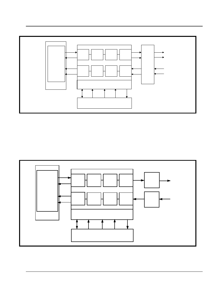
·Á
·Á
·Á
·Á
DS3 UNI FOR ATM
XRT7245
PRELIMINARY
REV. 1.03
33
If the user intends to interface the UNI to an optical
DS3 line, then the user can operate the UNI in the
"unipolar" mode. Additionally, the user would connect
the single-rail output pin of the UNI (TxPOS) to the
"Electrical" input of an "Electrical to Optical" converter;
and connect the single-rail input pin of the UNI
(RxPOS) to the "Electrical" output of an "Optical to
Electrical" converter. The "Electrical to Optical" and
"Optical to Electrical" converters are "entities" that
handle the translation between the electronic and
photonic modes. Figure 4 presents an illustration of the
"System Level" interfacing of the XRT7245 DS3 UNI,
when the DS3 line signal is transmitted over an
optical medium.
F
IGURE
3. S
YSTEM
L
EVEL
I
NTERFACING
OF
THE
XRT7245 DS3 UNI (DS3 D
ATA
IS
TRANSMITTED
OVER
C
OPPER
M
EDIUM
)
ATM
Layer
Processor
Line
Interface
Unit
Microprocessor
Interface
XR-T7245
TxData
[15:0]
RxData
[15:0]
To/From
Far End
DS3 UNI
TxPOS
TxNEG
RxPOS
RxNEG
ATM Switch
Local "Housekeeping" Processor
D[15:0]
WRB_RW ALE_AS
RDS_DS
Rdy_Dtck
TxClav
RxClav
Transmit
Utopia
Interface
Block
Transmit
Cell
Processor
Transmit
PLCP
Processor
Transmit
DS3
Framer
Receive
Cell
Processor
Receive
Utopia
Interface
Block
Receive
PLCP
Processor
Receive
DS3
Framer
F
IGURE
4. S
YSTEM
L
EVEL
I
NTERFACING
OF
THE
XRT7245 DS3 UNI
(DS3
DATA
IS
TRANSMITTED
OVER
O
PTICAL
F
IBER
ATM
Layer
Processor
Electrical
to
Optical
Converter
Microprocessor
Interface
XR-T7245
TxData
[15:0]
To/From
Far End
DS3 UNI
TxPOS
RxPOS
ATM Switch
Local "Housekeeping" Processor
D[15:0]
WRB_RW
ALE_AS
RDS_DS
Rdy_Dtck
TxClav
RxClav
Transmit
Utopia
Interface
Block
Transmit
Cell
Processor
Transmit
PLCP
Processor
Transmit
DS3
Framer
Receive
Cell
Processor
Receive
Utopia
Interface
Block
Receive
PLCP
Processor
Receive
DS3
Framer
Optical
to
Electrical
Converter
RxData
[15:0]

XRT7245
DS3 UNI FOR ATM
·Á
·Á
·Á
·Á
PRELIMINARY
REV. 1.03
34
The remainder of this text will frequently refer to each
of these "entities" as:
∑
The ATM Layer Processor
∑
The Local Microprocessor
∑ The Line Interface Unit (LIU) IC
1.2
Internal Operation of the XRT7245 DS3
UNI device
Whenever an ATM switch, that has access to a DS3
line, needs to transmit ATM cell data to the "Far-End"
Terminal over the DS3 line, it will write the ATM cell
data into the Transmit UTOPIA Interface block of the
XRT7245 DS3 UNI device. Afterwards, the Transmit
UTOPIA Interface block will ultimately write this cell
data to an internal FIFO (referred to as Tx FIFO
throughout this document); where it can be read and
further processed by the Transmit Cell Processor. The
Transmit UTOPIA Interface block will also perform
some parity checking on the data that it receives from
the ATM Layer processor. Finally, the Transmit UTOPIA
Interface block will provide signaling to support data-
flow control between the ATM Layer Processor and
the UNI IC.
The Transmit Cell Processor block will read in the
ATM cell from the Tx FIFO. It will then (optionally)
proceed to take the first four octets of this cell and
compute the HEC byte from these bytes. Afterwards
the Transmit Cell Processor will insert this HEC byte
into the 5th octet position within the cell. The Transmit
Cell Processor will also (optionally) scramble the pay-
load portion of the cell (bytes 6 through 53) in order
to prevent user data from mimicing framing or control
bits/bytes. Once the cell has gone through this process
it will then be transferred to the Transmit PLCP
Processor (or Transmit DS3 Framer, if the "Direct
Mapped" ATM option is selected).
If the Tx FIFO (within the Transmit UTOPIA Interface
block) is depleted and has no (user) cells available,
then the Transmit Cell Processor will automatically
generate Idle cells. These Idle cells will be processed
in the exact same manner as are the user cells, prior
to transmission to the Transmit PLCP Processor (or
the Transmit DS3 Framer) block. The Transmit Cell
Processor has provisions to allow the user to generate
an OAM cell via software control.
Note: The OAM cells will be subjected to the same
processing (e.g., HEC Byte Calculation/Insertion and Cell
Payload Scrambling) as are user and Idle cells.
The Transmit PLCP Processor block will take 12 ATM
cells and pack them into a single PLCP frame. In addi-
tion to the ATM Cells, the PLCP frame will consists of
numerous overhead bytes and either a 13 or 14 nibble
trailer to frequency justify the PLCP frame to the
specified 8 kHz frame rate. Once these PLCP frames
have been formed they will be transferred to the
Transmit DS3 Framer.
The Transmit DS3 Framer block will take the PLCP
frame (or ATM cells, if the Direct-Mapped ATM option
was selected), and insert this data into the payload
portions of the outbound DS3 frame. The Transmit
DS3 Framer will also generate overhead (OH) bits
that support framing, performance monitoring (parity
bits), path maintenance data link as well as alarm and
status information originating from the "Near-End"
Receiver section of the UNI. The purpose of these
alarm and status information bits is to alert the "Far-
End" equipment that the "Near-End" UNI Receiver
has detected some problems in receiving data from
it. The Transmit DS3 Framer will output this DS3 data
stream to an off-chip LIU (Line Interface Unit) chip via
the TxPOS, TxNEG, and TxLineClk output pins. The
LIU chip will take on the responsibility of driving the
DS3 data out on the DS3 Transport Medium to the
"Far-End" Terminal.
Likewise, whenever ATM cell data arrives at the UNI,
over the DS3 line, the Receive DS3 Framer block will
synchronize itself to this incoming DS3 Data Stream
(containing ATM cells) via the RxPOS, RxNEG, and
RxLineClk input pins, and proceed to "strip off" and
process the OH bits of the DS3 frame. Once all of the
OH bits have been removed, the payload portion of
the received DS3 Frame should consist of either
PLCP frames or ATM cells (if the Direct-Mapped ATM
option was selected). The PLCP frames are transferred
to the Receive PLCP Processor and the "Direct-
Mapped" ATM Cells are sent onto the Receive Cell
Processor.
The Receive PLCP Processor block will take the
PLCP frame data and search for the A1 and A2
frame alignment bytes, in order to locate the PLCP
frame boundaries. Once PLCP framing is established,
the Receive PLCP Processor will proceed to check
and process the OH bytes, within the PLCP frame.
The PLCP Frames, along with framing information
are sent on to the Receive Cell Processor.
The Receive Cell Processor takes delineated PLCP
frames from the Receive PLCP Processor, and per-
forms the following operations:
∑ Cell Delineation
∑ HEC Byte Verification
The Receive Cell Processor takes the first four octets
of the cell (the header) and computes a HEC byte. The
Receive Cell Processor will then compare this com-
puted HEC value with that of the fifth octet, within the

·Á
·Á
·Á
·Á
DS3 UNI FOR ATM
XRT7245
PRELIMINARY
REV. 1.03
35
cell. If the two HEC values are equal, then the cell is
then retained for further processing. If the two HEC
values are not equal, then the cells with single-bit
errors are typically corrected. However, the cell is
optionally discarded if multiple-bit errors are detected.
∑ Cell Filtering
The Receive Cell Processor will optionally detect and
remove Idle Cells, and can be configured to filter User
and OAM cells based upon their header byte patterns.
∑ Cell De-Scrambling
The Receive Cell Processor will de-scramble the pay-
load portion of the cell (the 6th through the 53rd octet),
and pack these octets in with the cell header bytes,
and the HEC byte for transmission to the Receive
UTOPIA Interface block.
Once the ATM cells have gone through the cell delin-
eation, HEC Byte Verification, cell payload de-scram-
bling, and cell filtering processes, then they will be
written into the Rx FIFO, within the Receive UTOPIA
Interface Block.
The Receive UTOPIA Interface block (like its Transmit
counterpart) provides the industry standard ATM/PHY
interface functions. The Receive UTOPIA Interface
Block will inform the ATM Layer Processor when it is
holding ATM cell data within the RxFIFO that needs to
be read. The ATM Layer Processor can then read out
this cell data from the Receive UTOPIA Interface
block, and route it to the remainder of the ATM switch
for further processing.
XRT7245
DS3 UNI FOR ATM
·Á
·Á
·Á
·Á
PRELIMINARY
REV. 1.03
36
PRINCIPLE OF OPERATION
2.0 THE USER NETWORK
INTERFACE (UNI)
The term UNI refers to an interface between an ATM
user or end-point (e.g., workstations, bridges, routers,
private switches) and an ATM network node (typically
a switch). The UNI could conform to any of a number
of physical transmission media standards including
the synchronous as well as the plesiochronous digital
hierarchies. Figure 5 illustrates an example of a pos-
sible application of the XRT7245 UNI.
These Functional Blocks are:
∑
Microprocessor Interface and Programmable
Registers
∑
Test and Diagnostic Section
∑
Line Interface Drive and Scan Section
∑
Transmit Section
∑
Receive Section
∑ Performance Monitors
F
IGURE
5. A
N
E
XAMPLE
OF
AN
A
PPLICATION
OF
THE
XRT7245 UNI.
Video
Camera
MPEG
Encoder
Video
Monitor
MPEG
Decoder
Video
Camera
MPEG
Encoder
Video
Monitor
MPEG
Decoder
SAR
SAR
SAR
SAR
User Terminals
IEEE 802.5
Token Ring Network
Router
Local Area Network
(10BaseT)
User Terminals
Router
ATM
Switch
ATM
Switch
XR-T7245
DS3 UNI
MPEG Data
ATM Cells
ATM Cells
XR-T7245
DS3 UNI
TCP/IP
Data
Utopia
Data Bus
TCP/IP
Data
DS3 Transport
Medium
Utopia
Data Bus
User A
User B
User D
User C
DS3 LIU
DS3 LIU
Hub
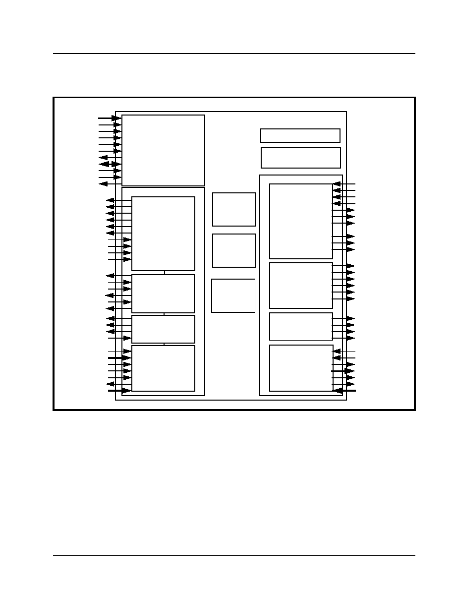
·Á
·Á
·Á
·Á
DS3 UNI FOR ATM
XRT7245
PRELIMINARY
REV. 1.03
37
Each of these functional blocks will be discussed in
detail below.
F
IGURE
6. F
UNCTIONAL
B
LOCK
D
IAGRAM
OF
THE
XRT7245 DS3 UNI.
Microprocessor Interface
(Programmable
Registers and Interrupt
Block)
Line I/F Drive and Scan
Transmit
DS3
Framer
Transmitter
Receiver
Receive
DS3
Framer
Performance
Monitor
Transmit
PLCP
Processor
Transmit Cell
Processor
Tx Utopia
Interface
Receive
PLCP
Processor
Receive Cell
Processor
Rx Utopia
Interface
A[8:0]
WrB_RW
RdB_DS
CSB*
ALE_AS
Reset
IntB*
D[15:0]
Width16
MOTO/Intel*
Rdy_Dtck
TxPOS
TxNEG
TxFrame
TxOHClk
TxLineClk
TxAISEn
TxFrameRef
TxInClk
TxOHIns
TxOH
TxPFrame
8kRef
StuffCtl
TxPOHFrame
TxPOH
TxPOHClk
TxCellTxed
TxGFCClk
TxGFCMSB
TxGFC
TxClk
TxData[15:0]
TxPrty
TxSoC
TxEnB
RxLineClk
RxNEG
RxPOS
RLOS
RxAIS
RxOHClk
RxOH[7:0]
RxLOS
RxFrame
RxOOF
RxPOHClk
RxPOH
RxPFrame
RxPLOF
RxPOOF
RxPOHFrame
RxCellRxed
RxGFCClk
RxGFCMSB
RxGFC
TxClav/TFullB
RFClk
RxEnB
RxPrty
RxData[15:0]
RxSoC
RxClav/RxEmpty
RxAddr[4:0]
TxAddr[4:0]
Transmit
DS3
Framer
Test and Diagnostic
FEAC
Processor
LAPD
Transceiver
XRT7245
DS3 UNI FOR ATM
·Á
·Á
·Á
·Á
PRELIMINARY
REV. 1.03
38
3.0 MICROPROCESSOR INTERFACE
SECTION AND ON-CHIP
PROGRAMMABLE REGISTERS
The Microprocessor Interface section supports com-
munication between the "local" microprocessor (µP)
and the UNI device. In particular, the Microprocessor
Interface section supports the following operations
between the local microprocessor and the UNI.
∑
The writing of configuration data into the UNI on-
chip (addressable) registers.
∑
The writing of "outbound" OAM cell data into the
"Transmit OAM Cell" Buffer (within the UNI).
∑
The writing of an "outbound" PMDL (Path Mainte-
nance Data Link) message into the "Transmit LAPD
Message" buffer (within the UNI).
∑
The UNI IC's generation of an Interrupt Request to
the µP.
∑
The µP's servicing of the interrupt request from the
UNI.
∑
The monitoring of the UNI system's "health" by
periodically reading the on-chip Performance Monitor
registers.
∑
The reading of an "inbound" OAM cell data from
the "Receive OAM Cell" buffer (within the UNI).
∑ The reading of an "inbound" PMDL Message from
the "Receive LAPD" Buffer (within the UNI).
Each of these operations (between the local micropro-
cessor and the UNI) will be discussed in some detail,
throughout this data sheet
Figure 7 presents a simple block diagram of the
Microprocessor Interface Section, within the UNI
device.
3.1
The Microprocessor Interface Signals
The UNI may be configured into a wide variety of
different operating modes and have its performance
monitored by software through a standard (local
"housekeeping") microprocessor, using data, address
and control signals.
Note: This local "housekeeping" Microprocessor should
not be confused with the ATM Layer Processor that inter-
faces to the UNI via the Transmit and Receive UTOPIA
Interface Blocks.
The local µP configures the UNI (into a desired oper-
ating mode) by writing data into specific addressable,
on-chip "Read/Write" registers; or on-chip RAM. The
microprocessor interface provide the signals which are
required for a general purpose microprocessor to read
or write data into these registers. The Microprocessor
Interface also supports "polled" and interrupt driven
environments. These interface signals are described
below in Table 1, 2, and 3. The microprocessor inter-
face can be configured to operate in the "Motorola"
mode or in the "Intel" mode. When the Microprocessor
Interface is operating in the "Motorola" mode, then
some of the control signals function in a manner as
required by the Motorola 68000 family of micropro-
cessors. Likewise, when the Microprocessor Interface
is operating in the "Intel" Mode, then some of these
Control Signals function in a manner as required by
the Intel 80xx family of microprocessors.
Table 1 lists and describes those Microprocessor Inter-
face signals whose role is constant across the two
F
IGURE
7. S
IMPLE
B
LOCK
D
IAGRAM
OF
M
ICROPROCESSOR
I
NTERFACE
BLOCK
OF
UNI
A[8:0]
WrB_RW
RdB_DS
CSB*
ALE_AS
Reset
IntB*
D[15:0]
Width16
MOTO
Rdy_Dtck
Microprocessor Interface
and
Programmable Registers

·Á
·Á
·Á
·Á
DS3 UNI FOR ATM
XRT7245
PRELIMINARY
REV. 1.03
39
modes. Table 2 describes the role of some of these
signals when the Microprocessor Interface is operat-
ing in the Intel Mode. Likewise, Table 3 describes the
role of these signals when the Microprocessor Inter-
face is operating in the Motorola Mode.
T
ABLE
1: D
ESCRIPTION
OF
THE
M
ICROPROCESSOR
I
NTERFACE
S
IGNALS
THAT
EXHIBIT
CONSTANT
ROLES
IN
BOTH
THE
"I
NTEL
"
AND
"M
OTOROLA
" M
ODES
.
P
IN
N
AME
T
YPE
D
ESCRIPTION
MOTO
I
Selection input for Intel/Motorola
µ
P Interface. Setting this pin to a logic "high" configures the
Microprocessor Interface to operate in the "Motorola" mode. Likewise, setting this pin to a logic
"low" configures the Microprocessor Interface to operate in the "Intel" Mode.
Width16
I
Select input for the Data Bus Width: Setting this pin to a logic "high" configures the width of the
Microprocessor Interface data bus width to be 16 bits. Likewise, setting this pin to a logic "low"
selects a data bus width of 8 bits.
D[15:0]
I/O
Bi-Directional Data Bus for register read or write operations.
Note: If the "Width16" input is "low", then only D[7:0] is active.
A[8:0]
I
Nine Bit Address Bus Input: This nine bit Address Bus is provided to allow the user to select an
on-chip register or on-chip RAM location.
CSB
I
Chip Select Input. This "active low" signal selects the Microprocessor Interface of the UNI device
and enables read/write operations with the on-chip registers/on-chip RAM.
IntB
O
Interrupt Request Output: This "open-drain/active-low" output signal will inform the local
µ
P that
the UNI has an interrupt condition that needs servicing.
T
ABLE
2: P
IN
D
ESCRIPTION
OF
M
ICROPROCESSOR
I
NTERFACE
S
IGNALS
--W
HILE
THE
M
ICROPROCESSOR
I
NTERFACE
IS
O
PERATING
IN
THE
I
NTEL
M
ODE
.
P
IN
N
AME
E
QUIVALENT
P
IN IN
I
NTEL
E
NVIRONMENT
T
YPE
D
ESCRIPTION
ALE_AS
ALE
I
Address-Latch Enable: This "active-high" signal is used to latch the contents
on the address bus, A[8:0]. The contents of the Address Bus are latched into the
A[8:0] inputs on the falling edge of ALE_AS. Additionally, this signal can be used
to indicate the start of a burst cycle.
RdB_DS
RD*
I
Read Signal: This "active-low" input functions as the read signal from the local
µ
P. When this signal goes "low", the UNI Microprocessor Interface will place the
contents of the addressed register on the Data Bus pins (D[15:0]). The Data Bus
will be "tri-stated" once this input signal returns "high".
WRB_RW
WR*
I
Write Signal: This "active-low" input functions as the write signal from the local
µ
P. The contents of the Data Bus (D[15:0]) will be written into the addressed reg-
ister (via A[8:0]), on the rising edge of this signal.
Rdy_Dtck
READY*
O
Ready Output: This "active-low" signal is provided by the UNI device, and indi-
cates that the current read or write cycle is to be extended until this signal is
asserted. The local
µ
P will typically insert "WAIT" states until this signal is
asserted. This output will toggle "low" when the device is ready for the next Read
or Write cycle.

XRT7245
DS3 UNI FOR ATM
·Á
·Á
·Á
·Á
PRELIMINARY
REV. 1.03
40
3.2
Interfacing the XRT7245 DS3 UNI to the
Local µC/µP Over Via the Microprocessor
Interface Block
The Microprocessor Interface block, within the UNI
device is very flexible and provides the following
options to the user.
∑
To interface the UNI device to a µC/µP over an 8-bit
or 16-bit wide bi-directional data bus.
∑
To interface the UNI to an Intel-type or Motorola-
type µC/µP.
∑ To transfer data (between the UNI IC and the µC/µP)
via the Programmed I/O or Burst Mode
Each of the options are discussed in detail below.
Section 3.2.1 will discussed the issues associated
with interfacing the UNI to a µC/µP over an 8-bit wide
and 16-bit wide bi-directional data bus. Afterwards,
Section 3.2.2 will discuss Data Access (e.g.,
Programmed I/O and Burst) Mode when interfaced to
both Motorola-type and Intel-type µC/µP.
3.2.1
Interfacing the XRT7245 DS3 UNI to the
Microprocessor Over an 8 and 16 Bit
Wide Bi-Directional Data Bus
The XRT7245 DS3 UNI Microprocessor Interface
permits the user to interface it to a µC/µP over an 8 or
16-bit wide bi-directional data bus.
If the user wishes to interface the UNI to a µC/µP
over an 8-bit wide bi-directional data bus, then he/
she should tie the "Width16" input pin to GND. In this
mode, only data bus pins: D0 through D7 will be active.
The remaining eight data bus pins (e.g., D8 through
D15) will be inactive.
Conversely, if the user wishes to interface the UNI to
a µC/µP over a 16-bit bi-directional data bus, then he/
she should tie the "Width16" input pin to VDD. In this
mode, all of the data bus pins: D0 through D15 will be
active.
The next two sections present issues associated with
interfacing the DS3 UNI to the µC/µP over an 8-bit
wide and 16-bit wide bi-directional data bus, respec-
tively.
T
ABLE
3: P
IN
D
ESCRIPTION
OF
THE
M
ICROPROCESSOR
I
NTERFACE
S
IGNALS
WHILE
THE
M
ICROPROCESSOR
I
NTERFACE
IS
OPERATING
IN
THE
M
OTOROLA
M
ODE
P
IN
N
AME
E
QUIVALENT
P
IN
IN
M
OTOROLA
E
NVIRONMENT
T
YPE
D
ESCRIPTION
ALE_AS
AS*
I
Address Strobe: This "active-low" signal is used to latch the contents on the
address bus input pins: A[8:0] into the Microprocessor Interface circuitry. The
contents of the Address Bus are latched into the UNI device on the rising edge of
the ALE_AS signal. This signal can also be used to indicate the start of a burst
cycle.
RdB_DS
DS*
I
Data Strobe: This signal latches the contents of the bi-directional data bus pins
into the Addressed Register (within the UNI) during a Write Cycle.
WRB_RW
R/W*
I
Read/Write* Input: When this pin is "high", it indicates a Read Cycle. When this
pin is "low", it indicates a Write cycle.
Rdy_Dtck
DTACK*
O
Data Transfer Acknowledge: The UNI device asserts DTACK* in order to
inform the CPU that the present READ or WRITE cycle is nearly complete. The
68000 family of CPUs requires this signal from its peripheral devices, in order to
quickly and properly complete a READ or WRITE cycle.

·Á
·Á
·Á
·Á
DS3 UNI FOR ATM
XRT7245
PRELIMINARY
REV. 1.03
41
3.2.1.1
Interfacing the UNI to the µC/µP Over
an 8-Bit Wide Bi-Directional Data Bus.
In general, interfacing the UNI to an "8-bit" µC/µP is
quite straight-forward. This is because most of the
registers, within the UNI, are 8-bits wide. Further, in
this mode, the µC/µP can read or write data into both
even and odd numbered addresses within the UNI
address space.
Reading Performance Monitor (PMON) Registers
The only awkward issue that the user should be wary
of (while operating in the "8-bit" mode) occurs when-
ever the µC/µP needs to read the contents of one of
the PMON (Performance Monitor) registers.
The XRT7245 DS3 UNI Device consists of the following
PMON Registers.
∑
PMON LCV Event Count Register
∑
PMON Framing Error Event Count Register
∑
PMON Received FEBE Event Count Register
∑
PMON Parity Error Event Count Register
∑
PMON Received Single-Bit HEC Error Count
Register
∑
PMON Received Multiple-Bit HEC Error Count
Register
∑
PMON Received Idle Cell Count Register
∑
PMON Received Valid Cell Count Register
∑
PMON Discarded Cell Count Register
∑
PMON Transmitted Idle Cell Count Register
∑ PMON Transmitted Valid Cell Count Register.
Unlike most of the registers within the UNI, the
PMON registers are "16-bit" registers (or 16-bits
wide). Table 4, lists each of these PMON registers as
consisting of two 8-bit registers. One of these "8-bit"
register is labeled "MSB" (or Most Significant Byte")
and the other register is labeled "LSB" (or Least
Significant Byte). When an "8-bit" PMON Register is
concatenated with its "companion 8-bit" PMON Reg-
ister, one obtains the "full 16-bit expression" within
that PMON Register.
The consequence of having these 16-bit registers is
that an "8-bit" µC/µP will have to perform two consec-
utive read operations in order to read in the full 16-bit
expression contained within a given PMON register.
To complicate matters, these PMON Registers are
"Reset-Upon-Read" registers. More specifically,
these PMON Register are "Reset-Upon-Read" in the
sense that, the entire "16-bit" contents, within a given
PMON Register is reset, as soon as an "8-bit" µC/µP
reads in either "byte" of this "two-byte" (e.g., 16 bit)
expression.
For Example
Consider that an "8-bit" µC/µP needs to read in the
"PMON LCV Event Count" Register. In order to ac-
complish this task, the 8-bit µC/µP is going to have to
read in the contents of "PMON LCV Event Count
Register--MSB" (located at Address = 0x40) and the
contents of the "PMON LCV Event Count Register--
LSB (located at Address = 0x41). These two "eight-
bit" registers, when concatenated together, make up
the "PMON LCV Event Count" Register.
If the 8-bit µC/µP reads in the "PMON LCV Event
Count--LSB" register first; then the entire "PMON
LCV Event Count" register will be reset to 0x0000. As
a consequence, if the 8-bit µC/µP attempts to read in
the "PMON LCV Event Count-MSB" register in the
very next read cycle, it will read in the value 0x00.
The PMON Holding Register
In order to "get-around" this "Reset-Upon-Read"
problem, the XRT7245 DS3 UNI device includes a
special register, which permits "8-bit" µC/µP to read
in the full 16-bit contents of these PMON registers.
This special register is called the "PMON Holding"
Register; and is located at 0x56 within the UNI Ad-
dress space.
The way the PMON Holding register works is as fol-
lows. Whenever an "8-bit" µC/µP reads in one of the
bytes (of the "2-byte" PMON register); the contents of
the "unread" (e.g., other) byte will be stored in the
PMON Holding Register. Therefore, the "8-bit" µC/µP
must then read in the contents of the PMON Holding
Register in the very next read operation.
In Summary: Whenever an "8-bit" µC/µP needs to
read a PMON Register, it must execute the follow-
ing steps.
Step 1: Read in the contents of a given "8-bit" PMON
Register (it does not matter whether the µC/µP reads
in the "-MSB" or the "-LSB" register).
Step 2: Read in the contents of the "PMON Holding"
Register (located at Address = 0x56). This register
will contain the contents of the "other" byte.
3.2.1.2
Interfacing the UNI to the µC/µP Over a
16-Bit Wide Bi-Directional Data Bus
Whenever the XRT7245 DS3 UNI is interfaced to a
µC/µP over a 16-bit wide bi-directional data, then the
following statements are true.
1.
Each read and write operation will be accessing
two "Configuration Registers" at once.

XRT7245
DS3 UNI FOR ATM
·Á
·Á
·Á
·Á
PRELIMINARY
REV. 1.03
42
2.
The µC/µP can read in the contents of a given
Performance Monitor (PMON) register in a single
read cycle.
As a consequence, the PMON Holding Register is
not needed in the "16-bit" mode.
1.
All "Read" and "Write" operations are aligned to
"even-numbered" addresses, within the UNI
Address Space.
As a consequence, the least significant address bus
pin, A0 is ignored, whenever the UNI is operating in
the "16-bit" Mode.
3.2.2
Data Access Modes
As mentioned earlier, the Microprocessor Interface
block supports data transfer between the UNI and the
µC/µP (e.g., "Read" and "Write" operations) via two
modes: the "Programmed I/O" and the "Burst"
Modes. Each of these "Data Access" Modes are dis-
cussed in detail below.
3.2.2.1
Data Access using Programmed I/O
"Programmed I/O" is the conventional manner in
which a microprocessor exchanges data with a pe-
ripheral device. However, it is also the slowest meth-
od of data exchange between the UNI and the µC/
µP; as will be described in this text.
The next two sections present detailed information
on Programmed I/O Access, when the XRT7245 DS3
UNI is operating in the "Intel Mode" and in the "Motor-
ola Mode".
3.2.2.1.1
Programmed I/O Access in the
"Intel" Mode
If the XRT7245 DS3 UNI is interfaced to an "Intel-
type" µC/µP (e.g., the 80x86 family, etc.), then it
should be configured to operate in the "Intel" mode
(by tying the "MOTO" pin to ground). Intel-type
"Read" and "Write" operations are described below.
3.2.2.1.1.1
The Intel Mode Read Cycle
Whenever an Intel-type µC/µP wishes to read the con-
tents of a register or some location within the Receive
LAPD Message buffer or the Receive OAM Cell Buffer,
(within the UNI device), it should do the following.
1.
Place the address of the "target" register or
buffer location (within the UNI) on the Address
Bus input pins A[8:0].
2.
While the µC/µP is placing this address value on
the Address Bus, the Address Decoding circuitry
(within the user's system) should assert the CS*
(Chip Select) pin of the UNI, by toggling it "low".
This action enables further communcation
between the µC/µP and the UNI Microprocessor
Interface block.
3.
Toggle the ALE_AS (Address Latch Enable)
input pin "high". This step enables the "Address
Bus" input drivers, within the Microprocessor
Interface block of the UNI.
4.
After allowing the data on the Address Bus pins
to settle (by waiting the appropriate "Address"
Data Setup time"), the µC/µP should toggle the
ALE_AS pin "low". This step causes the UNI
device to "latch" the contents of the "Address
Bus" into its internal circuitry. At this point, the
address of the register or buffer locations (within
the UNI), has now been selected.
5.
Next, the µC/µP should indicates that this current
bus cycle is a "Read" Operation by toggling the
RdB_DS (Read Strobe) input pin "low". This
action also enables the bi-directional data bus
output drivers of the UNI device. At this point, the
"bi-directional" data bus output drivers will pro-
ceed to drive the contents of the "latched
addressed" register (or buffer location) onto the
bi-directional data bus, D[15:0].
6.
Immediately after the µC/µP toggles the "Read
Strobe" signal "low", the UNI device will toggle
the Rdy_Dtck output pin "low". The UNI device
does this in order to inform the µC/µP that the
data (to be read from the data bus) is "NOT
READY" to be "latched" into the µC/µP.
7.
After some settling time, the data on the "bi-
directional" data bus will stabilize and can be
read by the µC/µP. The XRT7245 DS3 UNI will
indicate that this data can be read by toggling the
Rdy_Dtck (READY) signal "high".
8.
After the µC/µP detects the Rdy_Dtck signal
(from the XRT7245 DS3 UNI), it can then termi-
nate the Read Cycle by toggling the RdB_DS
(Read Strobe) input pin "high".
Figure 8 presents a timing diagram which illustrates
the behavior of the Microprocessor Interface signals,
during an "Intel-type" Programmed I/O Read Operation.
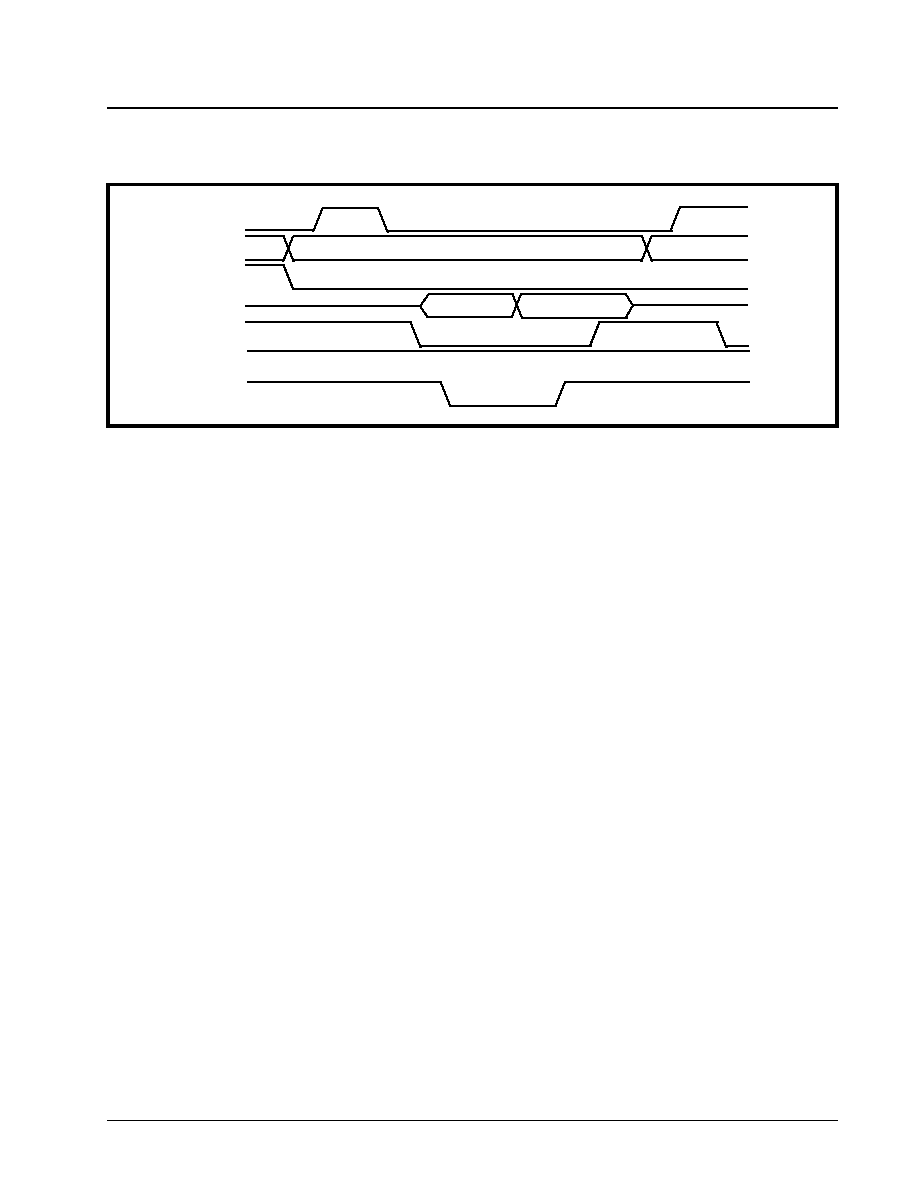
·Á
·Á
·Á
·Á
DS3 UNI FOR ATM
XRT7245
PRELIMINARY
REV. 1.03
43
3.2.2.1.1.2
The Intel Mode Write Cycle
Whenever an Intel-type µC/µP wishes to write a byte
or word of data into a register or buffer location, with-
in the UNI, it should do the following.
1.
Assert the ALE_AS (Address Latch Enable) input
pin by toggling it "high". When the µC/µP asserts
the ALE_AS input pin, it enables the "Address
Bus Input Drivers" within the UNI chip.
2.
Place the address of the "target" register or
buffer location (within the UNI), on the Address
Bus input pins, A[8:0].
3.
While the µC/µP is placing this address value
onto the Address Bus, the Address Decoding cir-
cuitry (within the user's system) should assert
the CS* input pin of the UNI device by toggling it
"low". This step enables further communication
between the µC/µP and the UNI Microprocessor
Interface block.
4.
After allowing the data on the Address Bus pins
to settle (by waiting the appropriate "Address
Setup" time); the µC/µP should toggle the
ALE_AS input pin "low". This step causes the
UNI device to "latch" the contents of the "Address
Bus" into its internal circuitry. At this point, the
address of the register or buffer location (within
the UNI), has now been selected.
5.
Next, the µC/µP should indicate that this current
bus cycle is a "Write" Operation; by toggling the
WRB_RW (Write Strobe) input pin "low". This
action also enables the "bi-directional" data bus
input drivers of the UNI device.
6.
The µC/µP should then place the byte or word
that it intends to write into the "target" register, on
the bi-directional data bus, D[15:0].
7.
After waiting the appropriate amount of time, for
the data (on the bi-directional data bus) to settle;
the µC/µP should toggle the WRB_RW (Write
Strobe) input pin "high". This action accom-
plishes two things:
a.
It latches the contents of the bi-directional
data bus into the XRT7245 DS3 UNI Micro-
processor Interface block.
b.
It terminates the write cycle.
Figure 9 presents a timing diagram which illustrates
the behavior of the Microprocessor Interface signals,
during an "Intel-type" Programmed I/O Write Operation.
F
IGURE
8. B
EHAVIOR
OF
M
ICROPROCESSOR
I
NTERFACE
SIGNALS
DURING
AN
"I
NTEL
-
TYPE
" P
ROGRAMMED
I/O R
EAD
O
PERATION
.
ALE_AS
RDB_DS
A[8:0]
CS*
D[15:0]
Rdy_Dtck
Not Valid
Valid
Address of Target Register
WRB_RW
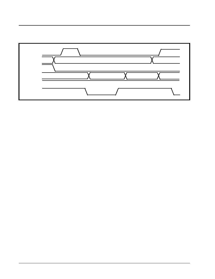
XRT7245
DS3 UNI FOR ATM
·Á
·Á
·Á
·Á
PRELIMINARY
REV. 1.03
44
3.2.2.1.2
Programmed I/O Access in the
Motorola Mode
If the XRT7245 DS3 UNI is interfaced to a "Motorola-
type" µC/µP (e.g., the MC680X0 family, etc.); it
should be configured to operate in the "Motorola"
mode (by tying the "MOTO" pin to Vcc). Motorola-
type Programmed I/O "Read" and "Write" operations
are described below.
3.2.2.1.2.1
The Motorola Mode Read Cycle
Whenever a "Motorola-type" µC/µP wishes to read
the contents of a register or some location within the
Receive LAPD Message or Receive OAM Cell Buffer,
(within the UNI device) it should do the following.
1.
Assert the ALE_AS (Address-Strobe) input pin
by toggling it low. This step enables the Address
Bus input drivers, within the Microprocessor
Interface Block of the UNI IC.
2.
Place the address of the "target" register (or
buffer location) within the UNI, on the Address
Bus input pins, A[8:0].
3.
At the same time, the Address Decoding circuitry
(within the user's system) should assert the CS*
(Chip Select) input pin of the UNI device, by tog-
gling it "low". This action enables further commu-
nication between the µC/µP and the UNI Micro-
processor Interface block.
4.
After allowing the data on the Address Bus pins
to settle (by waiting the appropriate "Address
Setup" time), the µC/µP should toggle the
ALE_AS input pin "high". This step causes the
UNI device to latch the contents of the "Address
Bus" into its internal circuitry. At this point, the
address of the register or buffer location (within
the UNI) has now been selected.
5.
Further, the µC/µP should indicate that this cycle
is a "Read" cycle by setting the WRB_RW (R/W*)
input pin "high".
6.
Next the µC/µP should initiate the current bus
cycle by toggling the RdB_DS (Data Strobe) input
pin "low". This step enables the bi-directional data
bus output drivers, within the XRT7245 DS3 UNI
device. At this point, the bi-directional data bus
output drivers will proceed to driver the contents
of the "Address" register onto the bi-directional
data bus, D[15:0].
7.
After some settling time, the data on the "bi-
directional" data bus will stabilize and can be
read by the µC/µP. The XRT7245 DS3 UNI will
indicate that this data can be read by asserting
the Rdy_Dtck (DTACK) signal.
8.
After the µC/µP detects the Rdy_Dtck signal
(from the XRT7245 DS3 UNI) it will terminate the
Read Cycle by toggling the "RdB_DS" (Data
Strobe) input pin "high".
Figure 10 presents a timing diagram which illustrates
the behavior of the Microprocessor Interface signals
during a "Motorola-type" Programmed I/O Read
Operation.
F
IGURE
9. B
EHAVIOR
OF
THE
M
ICROPROCESSOR
I
NTERFACE
S
IGNALS
,
DURING
AN
"I
NTEL
-
TYPE
" P
ROGRAMMED
I/O W
RITE
O
PERATION
.
ALE_AS
A[8:0]
CS*
D[15:0]
WRB_RW
Data to be Written
Address of Target Register
RdB_DS
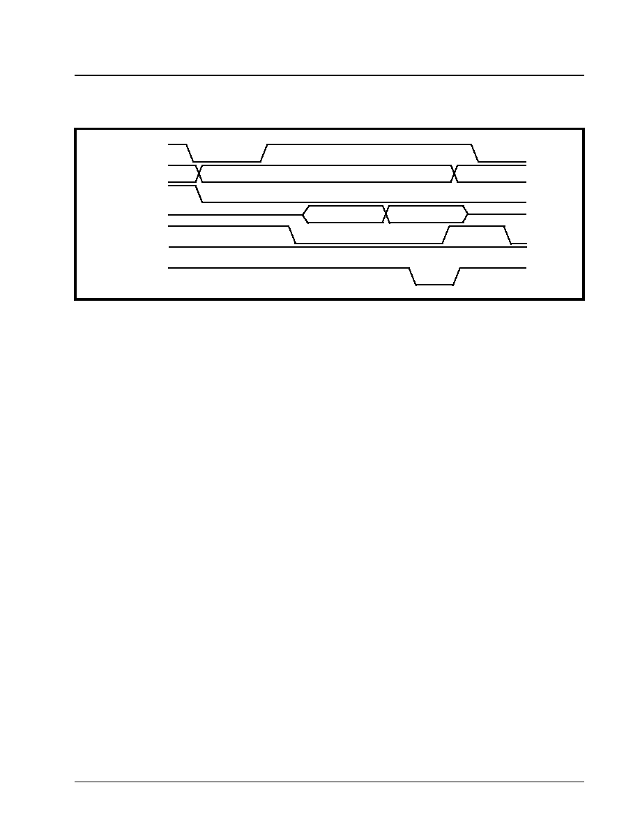
·Á
·Á
·Á
·Á
DS3 UNI FOR ATM
XRT7245
PRELIMINARY
REV. 1.03
45
3.2.2.1.2.2
The Motorola Mode Write Cycle
Whenever a Motorola-type µC/µP wishes to write a
byte or word of data into a register or buffer location,
within the UNI, it should do the following.
1.
Assert the ALE_AS (Address Select) input pin by
toggling it "low". This step enables the "Address
Bus" input drivers (within the UNI chip).
2.
Place the address of the "target" register or
buffer location (within the UNI), on the Address
Bus input pins, A[8:0].
3.
While the µC/µP is placing this address value
onto the Address Bus, the Address-Decoding cir-
cuitry (within the user's system) should assert
the CS* (Chip Select) input pins of the UNI by
toggling it "low". This step enables further com-
munication between the µC/µP and the UNI
Microprocessor Interface block.
4.
After allowing the data on the Address Bus pins
to settle (by waiting the appropriate "Address
Setup" time), the µC/µP should toggle the
ALE_AS input pin "high". This step causes the
UNI device to "latch" the contents of the "Address
Bus" into its own circuitry. At this point, the
Address of the register or buffer location (within
the UNI), has now been selected.
5.
Further, the µC/µP should indicate that this cur-
rent bus cycle is a "Write" operation by toggling
the WRB_RW (R/W*) input pin "low".
6.
The µC/µP should then place the byte or word
that it intends to write into the "target" register, on
the bi-directional data bus, D[15:0].
7.
Next, the µC/µP should initiate the bus cycle by
toggling the RdB_DS (Data Strobe) input pin
"low". When the XRT7245 DS3 UNI device
senses that the WRB_RW (R/W*) input pin is
"high" and that the RdB_DS (Data Strobe) input
pin has toggled "low", it will enable the "input
drivers" of the bidrectional data bus, D[15:0].
8.
After waiting the appropriate time, for this newly
placed data to settle on the bi-directional data
bus (e.g., the "Data Setup" time) the UNI will
assert the Rdy_Dtck output signal.
9.
After the µC/µP detects the Rdy_Dtck signal
(from the UNI), the µC/µP should toggle the
RdB_DS input pin "high". This action accom-
plishes two things.
a.
It latches the contents of the bi-directional
data bus into the XRT7245 DS3 Micropro-
cessor Interface block.
b.
It terminates the "Write" cycle.
Figure 11 presents a timing diagram which illustrates
the behavior of the Microprocessor Interface signals,
during a "Motorola-type" Programmed I/O Write
Operation.
F
IGURE
10. I
LLUSTRATION
OF
THE
B
EHAVIOR
OF
M
ICROPROCESSOR
I
NTERFACE
SIGNALS
,
DURING
A
"M
OTOROLA
-
TYPE
" P
ROGRAMMED
I/O R
EAD
O
PERATION
.
ALE_AS
RDB_DS
A[8:0]
CS*
D[15:0]
Rdy_Dtck
Not Valid
Valid Data
Address of Target Register
WRB_RW
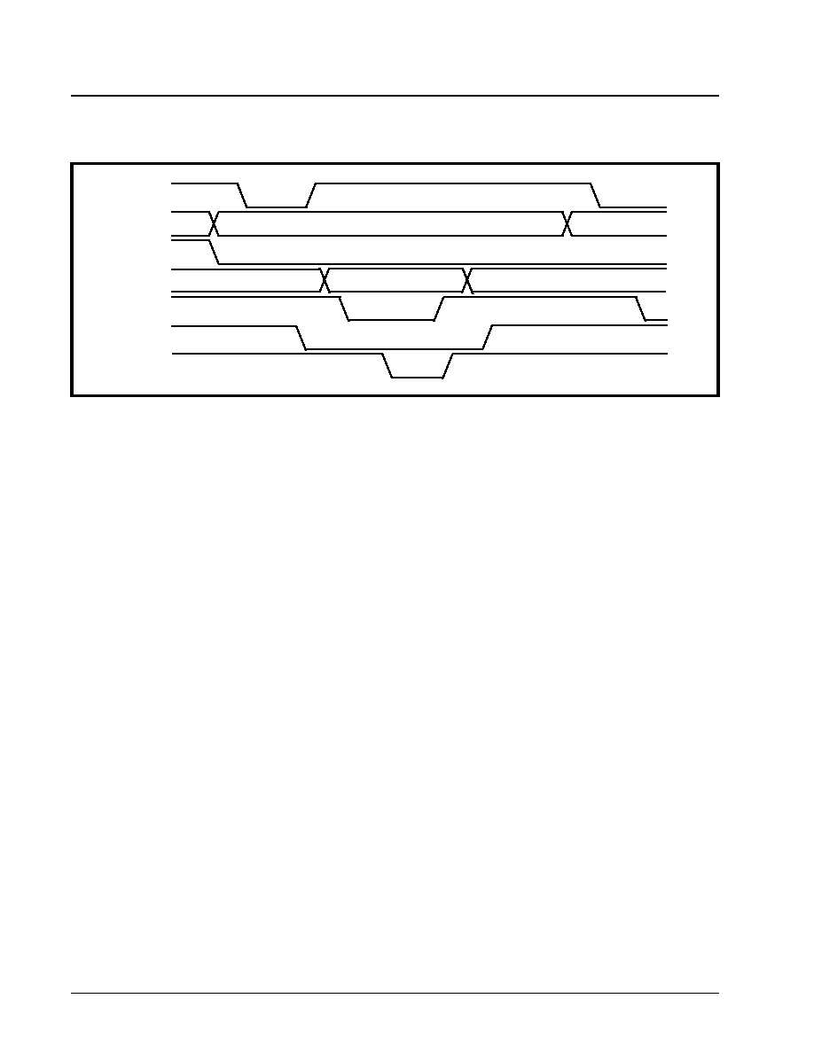
XRT7245
DS3 UNI FOR ATM
·Á
·Á
·Á
·Á
PRELIMINARY
REV. 1.03
46
3.2.2.2
Data Access Using Burst Mode I/O
Burst Mode I/O access is a much faster way to transfer
data between the µC/µP and the Microprocessor Inter-
face (of the XRT7245 DS3 UNI), than Programmed I/O.
The reason why Burst Mode I/O is so much faster
follows.
Data is placed upon the Address Bus input pins
A[8:0]; only for the very first access, within a given
burst access. The remaining read or write operations
(within this burst access) do not require the place-
ment of the Address Data on the Address Data Bus.
As a consequence, the user does not have to wait
through the "Address Setup" and "Hold" times; for
each of these Read/Write operation, within the
"Burst" Access.
It is important to note that there are some limitations
associated with Burst Mode I/O Operations.
1.
All cycles within the Burst Access, must be either
"all Read" or "all Write" cycles. No "mixing of
"Read" and "Write" cycles is permitted.
2.
A Burst Access can only be used when "Read" or
"Write" operations are to be employed over a
contiquous range of address locations, within the
UNI device.
3.
The very first "Read" or "Write" cycle, within a
burst access, must start at the "lowest" address
value, of the range of addresses to be accessed.
Subsequent operations will automatically be incre-
mented to the very next higher address value.
Examples of Burst Mode I/O operations are presented
below for read and write operations, with both "Intel-
type" and "Motorola-type" µC/µP.
3.2.2.2.1
Burst I/O Access in the Intel Mode
If the XRT7245 DS3 UNI is interfaced to an "Intel-
type" µC/µP (e.g., the 80x86 family, etc.), then it
should be configured to operate in the "Intel" mode
(by tying the "MOTO" pin to ground). Intel-type
"Read" and "Write" Burst I/O Access operations are
described below.
3.2.2.2.1.1
The "Intel-Mode" Read Burst Access
Whenever an "Intel-type" µC/µP wishes to read the
contents of numerous registers or buffer locations
over a "contiguous" range of addresses; then it
should do the following.
a.
Perform the initial "read" operation of the
burst access.
b.
Perform the remaining "read" operations of
the burst access.
c.
Terminate the "burst access" operation.
Each of these "operations" within the burst access
are described below.
3.2.2.2.1.1.1
The Initial Read Operation
The initial read operation of an "Intel-type" read burst
access is accomplished by executing a "Programmed
I/O" Read Cycle as summarized below.
A.
Execute a Single Ordinary (Programmed I/O)
Read Cycle, as described in Steps A.1
through A.7 below.
A.1
Place the address of the "initial-target" register
or buffer location (within the UNI) on the
Address Bus input pins A[8:0].
F
IGURE
11. I
LLUSTRATION
OF
THE
B
EHAVIOR
OF
THE
M
ICROPROCESSOR
I
NTERFACE
SIGNAL
,
DURING
A
"M
OTOROLA
-
TYPE
" P
ROGRAMMED
I/O W
RITE
O
PERATION
.
ALE_AS
A[8:0]
CS*
D[15:0]
RDB_DS
Rdy_Dtck
Data to be Written
Address of Target Register
WRB_RW
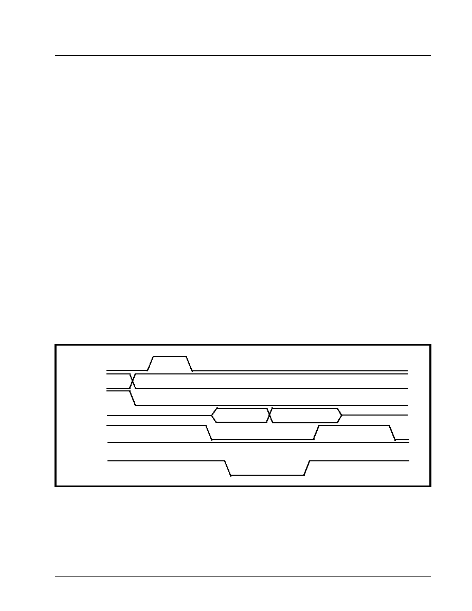
·Á
·Á
·Á
·Á
DS3 UNI FOR ATM
XRT7245
PRELIMINARY
REV. 1.03
47
A.2
While the µC/µP is placing this address value
onto the Address Bus, the Address Decoding
circuitry (within the user's system) should assert
the CS* input pin of the UNI, by toggling it
"low". This step enables further communication
between the µP/µC and the UNI Microproces-
sor Interface block.
A.3
Assert the ALE_AS (Address Latch Enable)
pin by toggling it "high". This step enables the
"Address Bus" input drivers, within the Micro-
processor Interface block of the UNI.
A.4
After allowing the data on the Address Bus
pins to settle (by waiting the appropriate
"Address" Data Setup time"), the µC/µP should
then toggle the ALE_AS pin "low". This step
latches the contents, on the Address Bus pins,
A[8:0], into the XRT7245 DS3 UNI Micropro-
cessor Interface block. At this point, the "initial"
address of the burst access has now been
selected.
Note: The ALE_AS input pin should remain "low" for the
remainder of this "Burst Access" operation.
A.5
Next, the µC/µP should indicate that this current
bus cycle is a "Read" Operation by toggling the
RdB_DS (Read Strobe) input pin "low". This
action also enables the "bi-directional" data bus
output drivers of the UNI device. At this point,
the bi-directional data bus output drivers will
proceed to drive the contents of the
"addressed" register onto the "bi-directional"
data bus, D[15:0].
A.6
Immediately after the µC/µP toggles the "Read
Strobe" signal "low", the UNI device will toggle
the Rdy_Dtck (READY) output pin "low". The
UNI device does this in order to inform the µC/
µP that the data (to be read from the data bus)
is "NOT READY" to be latched inot the µC/µP.
A.7
After some settling time, the data on the "bi-
directional" data bus will stabilize and can be
read by the µC/µP. The XRT7245 DS3 UNI will
indicate that this data is ready to be read, by
toggling the Rdy_Dtck (Ready) signal "high".
A.8
After the µC/µP detects the Rdy_Dtck signal
(from the XRT7245 DS3 UNI IC), it can then
will terminate the "Read" cycle by toggling the
RdB_DS (Read Strobe) input pin "high".
Figure 12 presents an illustration of the behavior of
the Microprocessor Interface Signals, during the "ini-
tial" Read Operation, within a Burst I/O Cycle; for an
Intel-type µC/µP.
At the completion of this initial read cycle, the µC/µP
has read in the contents of the first register or buffer
location (within the XRT7245 DS3 UNI) for this partic-
ular burst I/O access operation. In order to illustrate
how this "burst access operation" works, the byte (or
word) of data, that is being read in Figure 12 has
been labeled "Valid Data at Offset = 0x00". This label
indicates that the µC/µP is reading the very first register
(or buffer location) in this burst access operation.
3.2.2.2.1.1.2
The Subsequent Read Operations
The procedure that the µC/µP must use to perform
the remaining read cycles, within this Burst Access
operation, is presented below.
F
IGURE
12. B
EHAVIOR
OF
THE
M
ICROPROCESSOR
I
NTERFACE
S
IGNALS
,
DURING
THE
"I
NITIAL
" R
EAD
O
PERATION
OF A
B
URST
C
YCLE
(I
NTEL
T
YPE
P
ROCESSOR
).
ALE_AS
RDB_DS
A[8:0]
CS*
D[15:0]
Rdy_Dtck
Not Valid
Valid Data of Offset = 0x00
Address of "Initial" Target Register (Offset = 0x00)
WRB_RW
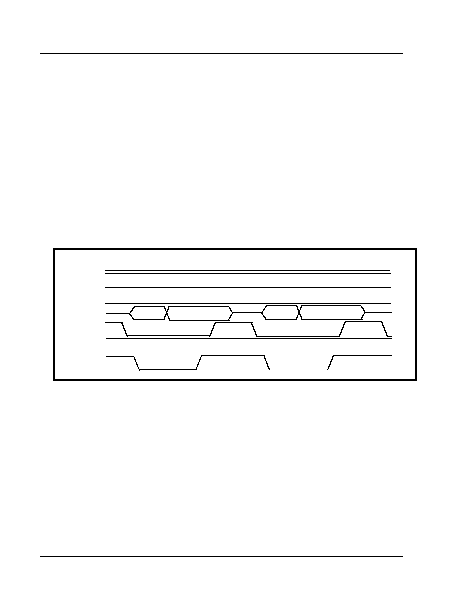
XRT7245
DS3 UNI FOR ATM
·Á
·Á
·Á
·Á
PRELIMINARY
REV. 1.03
48
B.
Execute each subsequent Read Cycles, as
described in Steps B.1 through B.3 below.
B.1
Without toggling the ALE_AS input pin (e.g.,
keeping it "low"); toggle the RdB_DS input pin
"low". This step accomplishes the following.
a.
The UNI will internally increments the
"latched address" value (within the Micro-
processor Interface circuitry).
b.
The output drivers of the "bi-directional"
data bus, D[15:0] are enabled. At some
time later, the register or buffer location
corresponding to the "incremented"
latched address value will be driven onto
the bidirectional data bus.
B.2
Immediately after the "Read Strobe" pin toggles
"low" the UNI IC will toggle the Rdy_Dtck
(READY) output pin "low" to indicate its "NOT
READY" status.
B.3
After some settling time, the data on the bi-
directional data bus will stabilize and can be
read by the µC/µP. The XRT7245 DS3 UNI will
indicate that this data is ready to be read by
toggling the Rdy_Dtck (READY) signal "high".
B.4
After the µC/µP detects the Rdy_Dtck signal
(from the XRT7245 DS3 UNI), it can then ter-
minates the "Read" cycle by toggling the
RdB_DS (Read Strobe) input pin "high".
For subsequent read operations, within this burst cycle,
the µP/µC simply repeats steps B.1 through B.3, as
illustrated in Figure 13.
In addition to the behavior of the Microprocessor In-
terface signals, Figure 13 also illustrates other points
regarding the "Burst Access Operation".
a.
The UNI internally increments the address
value, from the original "latched" value in
Figure 13. This is illustrated by the data,
appearing on the data bus, (for the first read
access) being labeled "Valid Data at Offset =
0x01"; and that for the second read access
being labeled "Valid Data at Offset = 0x02.".
b.
The UNI performs this "address increment-
ing" process even though there are no
changes in the Address Bus Data, A[8:0].
3.2.2.2.1.1.3
Terminating the Burst Access
Operation
The Burst Access Operation will be terminated upon
the rising edge of the ALE_AS input signal. At this
point the UNI will cease to internally increment the
"latched" address value. Further, the µC/µP is now
free to execute either a "Programmed I/O" access or
to start another "Burst Access" Operation with the
XRT7245 DS3 UNI.
F
IGURE
13. B
EHAVIOR
OF
THE
M
ICROPROCESSOR
I
NTERFACE
S
IGNALS
,
DURING
SUBSEQUENT
"R
EAD
" O
PERATIONS
WITHIN
THE
B
URST
I/O C
YCLE
.
ALE_AS
RDB_DS
A[8:0]
CS*
D[15:0]
Rdy_Dtck
Not Valid
Valid Data at Offset =0x01
WRB_RW
Not Valid
Valid Data at Offset =0x02
Address of "Initial" Target Register (Offset = 0x00)

·Á
·Á
·Á
·Á
DS3 UNI FOR ATM
XRT7245
PRELIMINARY
REV. 1.03
49
3.2.2.2.1.2
The "Intel-Mode" Write Burst
Access
Whenever an "Intel-type" µC/µP wishes to write data
into a "contiguous" range of addresses, then it should
do the following.
a.
Perform the initial "write" operation; of the
burst access.
b.
Perform the remaining "write" operations, of
the burst access.
c.
Terminate the burst access operation.
Each of these "operations" within the burst access
are described below.
3.2.2.2.1.2.1
The Initial Write Operation
The initial write operation of an "Intel-type" Write
Burst Access is accomplished by executing a "Pro-
grammed I/O" write cycle as summarized below.
A.
Execute a Single Ordinary (Programmed I/O)
Write cycle, as described in Steps A.1
through A.7 below.
A.1
Place the address of the "initial" target register
(or buffer location) within the UNI, on the
Address Bus pins, A[8:0].
A.2
At the same time, the "Address-Decoding" cir-
cuitry (within the user's system) should assert
the CS* (Chip Select) input pin of the UNI, by
toggling it "low". This step enables further com-
munication between the µC/µP and the UNI
Microprocessor Interface block.
A.3
Assert the ALE_AS (Address Latch Enable)
input pin "high". This step enables the Address
Bus input drivers, within the Microprocessor
Interface Block of the UNI.
A.4
After allowing the data on the Address Bus
pins to settle (by waiting the appropriate
"Address Setup" time); the µC/µP should then
toggle the ALE_AS input pin "low". This step
latches the contents, on the Address Bus pins,
A[8:0], into the XRT7245 DS3 UNI Micropro-
cessor Interface block. At this point, the "initial"
address of the "burst access" has now been
selected.
Note: The ALE_AS input pin should remain "low" for the
remainder of this "Burst I/O Access" operation.
A.5
Next, the µC/µP should indicate that this cur-
rent bus cycle is a "Write" operation by keeping
the RdB_DS pin "high" and toggling the
WRB_RW (Write Strobe) pin "low". This action
also enables the "bi-directional" data bus input
drivers of the UNI device.
A.6
The µC/µP places the byte (or word) that it
intends to write into the "target" register on the
"bidirectional data" bus, D[15:0].
A.7
After waiting the appropriate amount of time,
for the data (on the bi-directional data bus) to
settle, the µC/µP should toggle the WRB_RW
(Write Strobe) input pin "high". This action
accomplishes two things.
a.
It latches the contents of the bi-directional
data bus into the XRT7245 DS3 UNI
Microprocessor Interface Block.
b.
It terminates the write cycle.
Figure 14 presents a timing diagram which illustrates
the behavior of the Microprocessor Interface signals,
during the "initial" write operation within a Burst
Access, for an "Intel-type" µC/µP.
F
IGURE
14. B
EHAVIOR
OF
THE
M
ICROPROCESSOR
I
NTERFACE
SIGNALS
,
DURING
THE
"I
NITIAL
" W
RITE
O
PERATION
OF A
B
URST
C
YCLE
(I
NTEL
-
TYPE
P
ROCESSOR
)
ALE_AS
A[8:0]
CS*
D[15:0]
Not Valid
Valid Data at Offset =0x01
RDB_DS
Not Valid
Valid Data at Offset =0x02
WRB_RW
Address of "Initial" Target Register (Offset = 0x00)
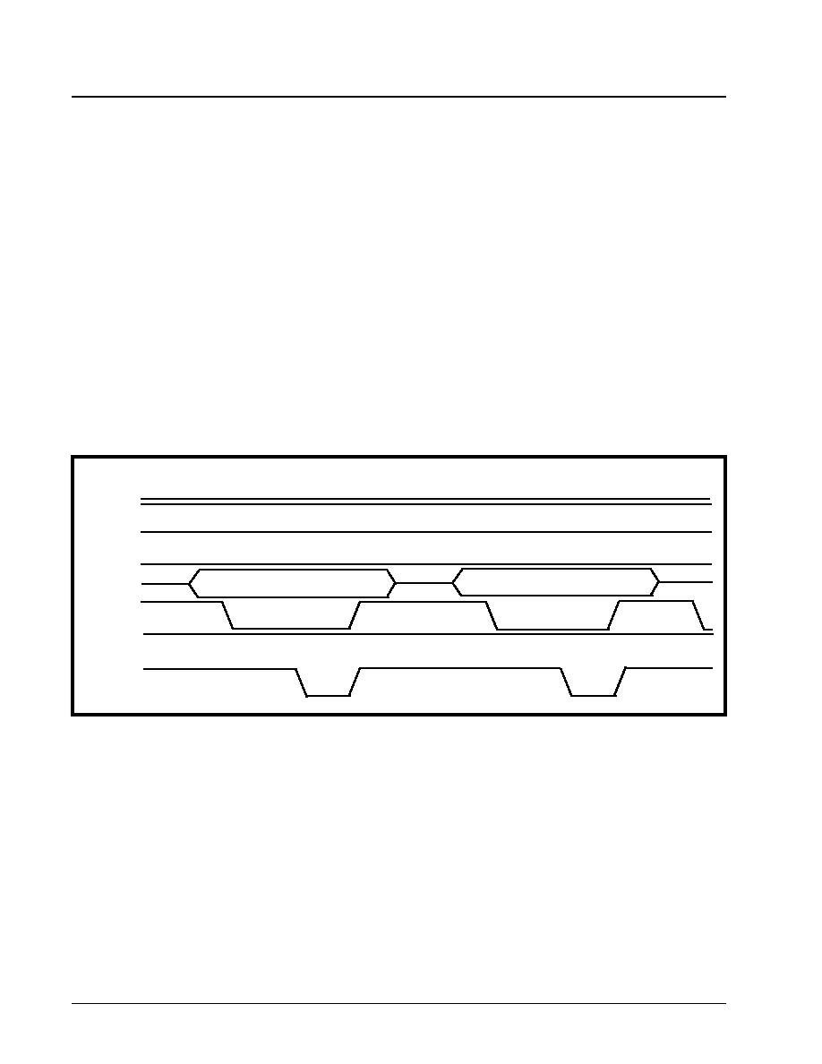
XRT7245
DS3 UNI FOR ATM
·Á
·Á
·Á
·Á
PRELIMINARY
REV. 1.03
50
At the completion of this initial write cycle, the µC/µP
has written a byte or word into the first register or
buffer location (within the XRT7245 DS3 UNI) for this
particular burst access operation. In order to illustrate
this point, the byte (or word) of data, that is being
written in Figure 14; has been labeled "Data to be
Written (Offset = 0x00)".
3.2.2.2.1.2.2
The Subsequent Write Operations
The procedure that the µC/µP must use to perform
the remaining write cycles, within this burst access
operation, is presented below.
B.
Execute each subsequent write cycle, as
described in Steps B.1 through B.3.
B.1
Without toggling the ALE_AS input pin (e.g.,
keeping it "low"); apply the value of the next
byte or word (to be written into the UNI) to the
bi-directional data bus pins, D[15:0].
B.2
Toggle the WRB_RW (Write Strobe) input pin
"low". This step accomplishes two things.
a.
It enables the input drivers of the bi-direc-
tional data bus.
b.
It causes the UNI to internally increment
the value of the "latched" address.
B.3
After waiting the appropriate amount of settling
time the data, in the internal data bus, will sta-
bilize and is ready to be latched into the UNI
Microprocessor Interface block. At this point,
the µC/µP should latch the data into the UNI by
toggling the WRB_RW input pin "high".
For subsequent write operations, within this burst I/O
access, the µC/µP simply repeats steps B.1 through
B.3, as illustrated in Figure 15.
3.2.2.2.1.2.3
Terminating the Burst I/O Access
Burst Access Operation will be terminated upon the
rising edge of the ALE_AS input signal. At this point
the UNI will cease to internally increment the "latched"
address value. Further, the µC/µP is now free to
execute either a "Programmed I/O" access or to start
another "Burst Access Operation" with the XRT7245
DS3 UNI.
3.2.2.2.2
Burst I/O Access in the Motorola
Mode
If the XRT7245 DS3 UNI is interfaced to a "Motorola-
type" µC/µP (e.g., the MC680x0 family, etc.), then it
should be configured to operate in the "Motorola" mode
(by tying the "MOTO" pin to VCC). Motorola-type
"Read" and "Write" Burst I/O Access operations are
described below.
3.2.2.2.2.1
The "Motorola-Mode" Read Burst
I/O Access Operation
Whenever a "Motorola-type" µC/µP wishes to read
the contents of numerous registers or buffer locations
over a "contiguous" range of addresses, then it
should do the following.
a.
Perform the initial "Read" operation of the
burst access.
b.
Perform the remaining "read" operations; in
the burst access.
c.
Terminate the "burst access" operation.
F
IGURE
15. B
EHAVIOR
OF
THE
M
ICROPROCESSOR
I
NTERFACE
S
IGNALS
,
DURING
SUBSEQUENT
"W
RITE
"
O
PERATIONS
WITHIN
THE
B
URST
I/O C
YCLE
.
ALE_AS
WRB_RW
A[8:0]
CS*
D[15:0]
Rdy_Dtck
Data Written at Offset =0x01
RDB_DS
Data Written at Offset =0x02
Address of "Initial" Target Register (Offset = 0x00)
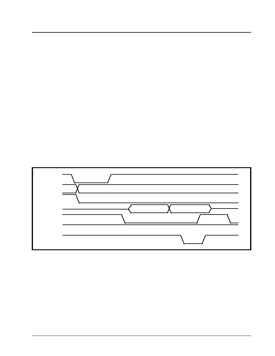
·Á
·Á
·Á
·Á
DS3 UNI FOR ATM
XRT7245
PRELIMINARY
REV. 1.03
51
Each of these operations, within the Burst Access
are discussed below.
3.2.2.2.2.1.1
The Initial Read Operation
The initial read operation of a "Motorola-type" read
burst access is accomplished by executing a "Pro-
grammed I/O Read" cycle, as summarized below.
A.
Execute a Single Ordinary (Programmed I/
O) Read Cycle, as described in steps A.1
through A.8 below.
A.1
Assert the ALE_AS (AS*) input pin by toggling
it "low". This step enables the "Address Bus"
input drivers (within the XRT7245 DS3 UNI)
within the UNI Microprocessor Interface Block.
A.2
Place the address of the "initial" target register
or buffer location (within the UNI), on the
Address Bus input pins, A[8:0].
A.3
At the same time, the Address-Decoding cir-
cuitry (within the user's system) should assert
the CS* (Chip Select) input pins of the UNI by
toggling it "low". This action enables further
communication between the µC/µP and the
UNI Microprocessor Interface block.
A.4
After allowing the data on the Address Bus
pins to settle (by waiting the appropriate
"Address Setup" time), the µC/µP should tog-
gle the ALE_AS input pin "high". This step
causes the UNI device to latch the contents of
the Address Bus into its internal circuitry. At
this point, the "initial" address of the burst
access has now been selected.
A.5
Further, the µC/µP should indicate that this
cycle is a "Read" cycle by setting the
WRB_RW (R/W*) input pin "high".
Figure 16 presents an illustration of the behavior of
the Microprocessor Interface Signals during the "ini-
tial" Read Operation, within a Burst I/O Cycle; for a
Motorola-type µC/µP.
At the completion of this initial read cycle, the µC/µP
has read in the contents of the first register or buffer
location (within the XRT7245 DS3 UNI) for this par-
ticular burst access operation. In order to illustrate
how this "burst I/O cycle" works, the byte (or word) of
data, that is being read in Figure 16, has been la-
beled "Valid Data at Offset = 0x00". This indicates
that the µC/µP is reading the very first register (or
buffer location) in this burst access.
3.2.2.2.2.1.2
The Subsequent Read Operations
The procedure that the µC/µP must use to perform
the remaining read cycles, within this Burst Access
operation, is presented below.
B.
Execute each subsequent Read Cycle, as
described in Steps B.1 through B.3, below.
B.1
Without toggling the ALE_AS input pin (e.g.,
keeping it "high"); toggle the RdB_DS (Data
Strobe) input pin "low". This step accomplishes
the following.
a.
The UNI internally increments the "latched
address" value (within the Microprocessor
Interface circuitry).
b.
The output drivers of the "bi-directional"
data bus (D[15:0]) are enabled. At some
time later, the register or buffer location
corresponding to the "incremented"
F
IGURE
16. B
EHAVIOR
OF
THE
M
ICROPROCESSOR
I
NTERFACE
S
IGNALS
,
DURING
THE
"I
NITIAL
" R
EAD
O
PERATION
OF A
B
URST
C
YCLE
(M
OTOROLA
T
YPE
P
ROCESSOR
).
ALE_AS
RDB_DS
A[8:0]
CS*
D[15:0]
Rdy_Dtck
Not Valid
Valid Data at Offset = 0x00
Address of "Initial" Target Register (Offset = 0x00)
WRB_RW
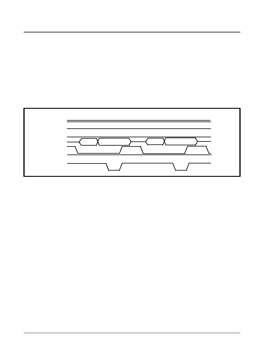
XRT7245
DS3 UNI FOR ATM
·Á
·Á
·Á
·Á
PRELIMINARY
REV. 1.03
52
latched address value will be driven onto
the bi-directional data bus.
Note: In order to insure that the XRT7245 DS3 UNI device
will interpret this signal as being a "Read" signal, the µC/µP
should keep the WRB_RW input pin "High".
B.2
After some settling time, the data on the bi-
directional data bus will stabilize and can be
read by the µC/µP. The XRT7245 DS3 UNI will
indicate that this data is ready to be read by
asserting the Rdy_Dtck (DTACK*) signal.
B.3
After the µC/µP detects the Rdy_Dtck signal
(from the SRT7245 DS3 UNI), it terminates the
"Read" cycle by toggling the RdB_DS (Data
Strobe) input pin "high".
For subsequent read operations, within this burst cycle,
the µC/µP simply repeats steps B.1 through B.3, as
illustrated in Figure 17.
3.2.2.2.2.1.3
Terminating the Burst Access
Operation
The Burst I/O Access will be terminated upon the fall-
ing edge of the ALE_AS input signal. At this point the
UNI will cease to internally increment the "latched"
address value. Further, the µC/µP is now free to exe-
cute either a "Programmed I/O" access or to start an-
other "Burst Access"Operation with the XRT7245
DS3 UNI.
3.2.2.2.2.2
The "Motorola-Mode" Write Burst
Access
Whenever a "Motorola-type" µC/µP wishes to write
the contents of numerous registers or buffer locations
over a "contiguous" range of addresses, then it
should do the following.
a.
Perform the initial "write" operation; of the
burst access.
b.
Perform the remaining "write" operations,
of the burst access.
c.
Terminate the burst access operation.
Each of these "operations" within the burst access
are described below.
3.2.2.2.2.2.1
The Initial Write Operation
The initial write operation of a "Motorola-type" Write
Burst Access is accomplished by executing a "Pro-
grammed I/O Write Cycle" as summarized below.
A.
Execute a Single Ordinary (Programmed I/O)
Write cycle, as described in Steps A.1
through A.7 below.
A.1
Assert the ALE_AS (Address Strobe) input pin
by toggling it "low". This step enables the
Address Bus input drivers (within the XRT7245
DS3 UNI).
A.2
Place the address of the "initial"target register
or buffer location (within the UNI), on the
Address Bus input pins, A[8:0].
A.3
At the same time, the Address-Decoding circuitry
(within the user's system) should assert the CS*
input pin of the UNI by toggling it "low". This step
enables further communication between the µC/
µP and the UNI Microprocessor Interface block.
A.4
After allowing the data on the Address Bus pins
to settle (by waiting the appropriate "Address
Setup" time), the µC/µP should toggle the
ALE_AS input pin "high". This step causes the
UNI device to "latch" the contents of the
F
IGURE
17. B
EHAVIOR
THE
M
ICROPROCESSOR
I
NTERFACE
S
IGNALS
,
DURING
SUBSEQUENT
"R
EAD
" O
PERATIONS
WITHIN
THE
B
URST
I/O C
YCLE
(M
OTOROLA
-
TYPE
µC/µP)
ALE_AS
RDB_DS
A[8:0]
CS*
D[15:0]
Rdy_Dtck
Not Valid
Valid Data at Offset =0x01
WRB_RW
Not Valid
Valid Data at Offset =0x02
Address of "Initial" Target Register (Offset = 0x00)
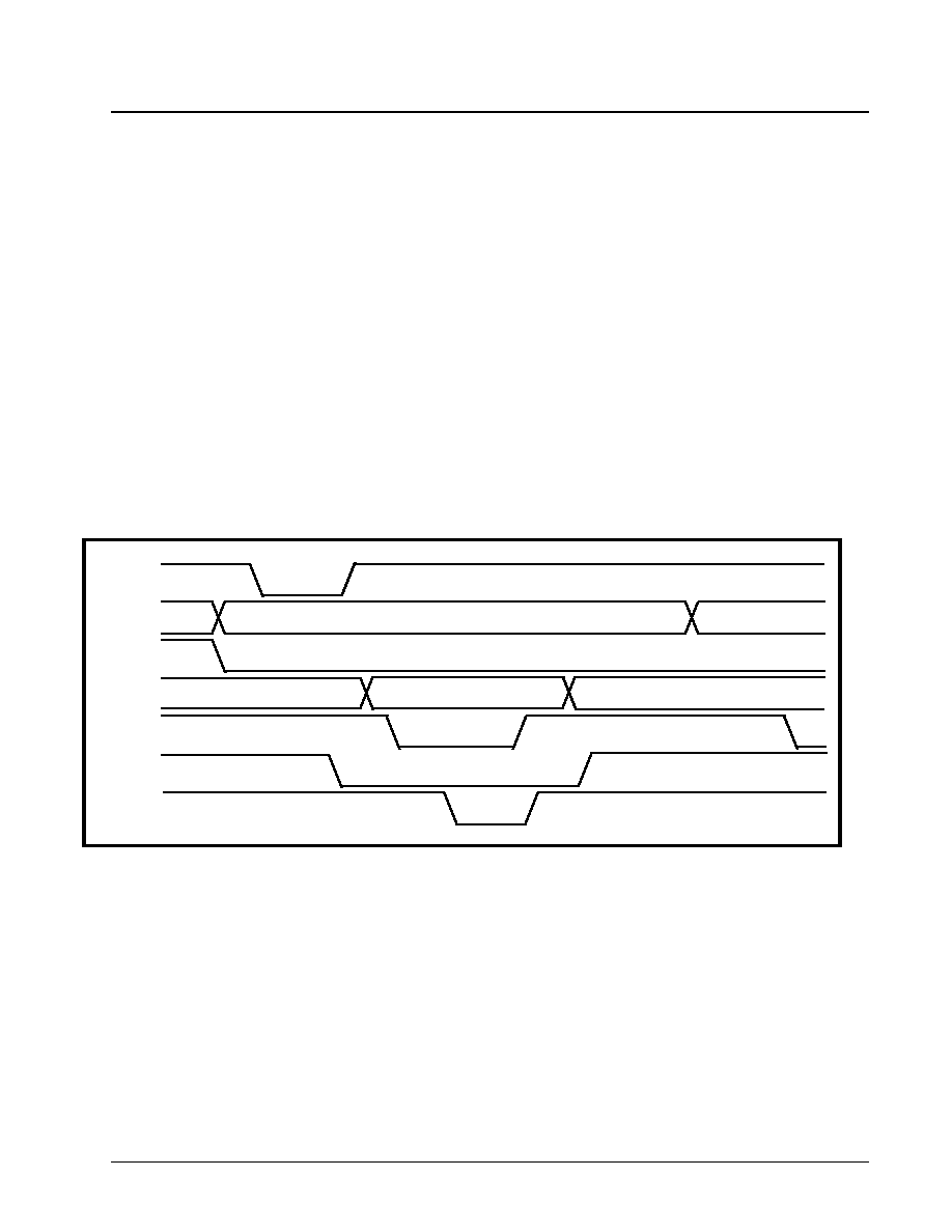
·Á
·Á
·Á
·Á
DS3 UNI FOR ATM
XRT7245
PRELIMINARY
REV. 1.03
53
"Address Bus" into its own circuitry. At this
point, the "initial" address of the burst access
has now been selected.
A.5
Further, the µC/µP should indicate that this
current bus cycle is a "Write" operation by tog-
gling the WRB_RW (R/W*) input pin "low".
A.6
The µC/µP should then place the byte or word
that it intends to write into the "target" register,
on the bidirectional data bus, D[15:0].
A.7
Next, the µC/µP should initiate the bus cycle by
toggling the RdB_DS (Data Strobe) input pin
"low". When the XRT7245 DS3 UNI device
senses that the WRB_RW input pin is "low",
and that the RdB_DS input pin has toggled
"low" it will enable the "input drivers" of the bidi-
rectional data bus, D[15:0].
A.8
After waiting the appropriate amount of time,
for this newly placed data to settle on the bi-
directional data bus( e.g., the "Data Setup"
time) the UNI will assert the Rdy_Dtck
(DTACK) output signal.
A.9
After the mC/mC detects the Rdy_Dtck signal
(from the UNI) it should toggle the RdB_DS
input pin "high". This action accomplishes two
things:
a.
It latches the contents of the bi-directional
data bus into the XRT7245 DS3 UNI
Microprocessor Interface block.
b.
It terminates the "Write" cycle.
Figure 18 presents a timing diagram which illustrates
the behavior of the Microprocessor Interface signals,
during the "Initial" write operation within a Burst
Access, for a "Motorola-type" µC/µP.
At the completion of this initial write cycle, the µC/µP
has written a byte or word into the first register or
buffer location (within the XRT7245 DS3 UNI) for this
particular burst I/O access. In order to illustrate how
this "burst I/O cycle" works, the byte (or word) of data,
that is being written in Figure 18, has been labeled
"Data to be Written (Offset = 0x00)."
3.2.2.2.2.2.2
The Subsequent Write Operations
The procedure that the µC/µP must use to perform
the remaining write cycles, within this burst access
operation, is presented below.
B.
Execute each subsequent write cycle, as
described in Steps B.1 through B.3
B.1
Without toggling the ALE_AS (Address Strobe)
input pin (e.g., keeping it "high"); apply the
value of the next byte or word (to be written into
the UNI) to the bi-directional data bus pins,
D[15:0].
B.2
toggle the RdB_DS (Data Strobe) input pin
"low". This step accomplishes the following.
a.
The UNI internally increments the "latched
address" value (within the Microprocessor
Interface).
F
IGURE
18. B
EHAVIOR
OF
THE
M
ICROPROCESSOR
I
NTERFACE
SIGNALS
,
DURING
THE
"I
NITIAL
" W
RITE
O
PERATION
OF A
B
URST
C
YCLE
(M
OTOROLA
-
TYPE
P
ROCESSOR
).
ALE_AS
A[8:0]
CS*
D[15:0]
RDB_DS
Rdy_Dtck
Data to be Written (Offset = 0x00)
Address of "Initial" Target Register (Offset = 0x00)
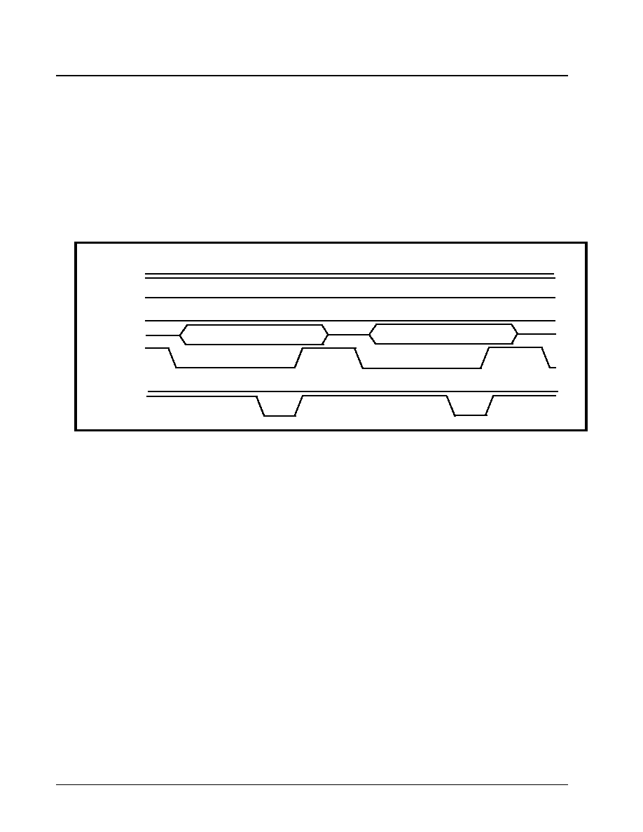
XRT7245
DS3 UNI FOR ATM
·Á
·Á
·Á
·Á
PRELIMINARY
REV. 1.03
54
b.
The input drivers of the bi-directional data
bus are enabled.
Note: In order to insure that the XRT7245 DS3 UNI device
will interpret this signal as being a "Write" signal, the µC/µP
should keep the WRB_RW input pin "low".
B.3
After some settling time, the data, in the inter-
nal data bus, will stabilize and is ready to be
latched into the UNI Microprocessor Interface
block. The Microprocessor Interface block will
indicate that this data is ready to be latched by
asserting the Rdy_Dtck (DTACK) output signal.
At this point, the µC/µP should latch the data
into the UNI by toggling the RDB_DS input pin
"high".
For subsequent write operations, within this burst I/O
access, the µC/µP simply repeats steps B.1 through
B.3 as illustrated in Figure 19.
3.2.2.2.2.2.3
Terminating the Burst I/O Access
The Burst I/O Access will be terminated upon the falling
edge of the ALE_AS input signal. At this point the UNI
will cease to internally increment the "latched" address
value. Further, the µC/µP is now free to execute
either a "Programmed I/O" access or to start another
"Burst I/O Access" with the XRT7245 DS3 UNI.
3.3
On-Chip Register Organization
The Microprocessor Interface section, within the UNI
device allows the user to do the following.
∑
Configure the UNI into a wide variety of operating
modes.
∑
Employ various features of the UNI device
∑
Perform status monitoring
∑ Enable/Disable and service Interrupt Conditions
All of these things are accomplished by reading from
or writing to the many on-chip registers, within the
UNI device. Table 4 lists each of these registers and
their corresponding address location within the UNI
address space.
3.3.1
UNI Register Addressing
The array of on-chip registers consists of a variety of
register types. These registers are denoted in Table 4,
as follows.
R/O--Read Only Registers
R/W--Read/Write Registers
RUR--Reset upon Read Registers
Sem--Semaphore Bit-field
Additionally some of these registers consists of both
R/O and R/W bit-fields. These registers are denoted
in Table 4 as "Combination of R/W and R/O".
The bit-format and definitions for each of these regis-
ters are presented in Section 3.3.2.
F
IGURE
19. B
EHAVIOR
OF
THE
M
ICROPROCESSOR
I
NTERFACE
S
IGNALS
,
DURING
SUBSEQUENT
"W
RITE
"
O
PERATIONS
WITH
THE
B
URST
I/O C
YCLE
(M
OTOROLA
-
TYPE
µC/µP).
ALE_AS
RDB_DS
A[8:0]
CS*
D[15:0]
Rdy_Dtck
Data Written at Offset =0x01
WRB_RW
Data Written at Offset =0x02
Address of "Initial" Target Register (Offset = 0x00)

·Á
·Á
·Á
·Á
DS3 UNI FOR ATM
XRT7245
PRELIMINARY
REV. 1.03
55
T
ABLE
4: R
EGISTER
A
DDRESSING
OF
THE
UNI P
ROGRAMMABLE
R
EGISTERS
A
DDRESS
R
EAD
M
ODE
R
EGISTER
W
RITE
M
ODE
R
EGISTER
R
EGISTER
T
YPE
00h
UNI Operating Mode Register
UNI Operating Mode Register
R/W
01h
UNI I/O Control Register
UNI I/O Control Register
R/W
02h
Part Number
R/O
03h
Version Number
R/O
04h
UNI Interrupt Enable Register
UNI Interrupt Enable Register
R/W
05h
UNI Interrupt Status Register
R/O
06h
Test Cell Control and Status Register
Test Cell Control and Status Register
(R/W portion only)
Combination of R/O
and R/W
07h
Future Use
Future Use
--
08h
Test Cell Header Byte 1
Test Cell Header Byte 1
R/W
09h
Test Cell Header Byte 2
Test Cell Header Byte 2
R/W
0Ah
Test Cell Header Byte 3
Test Cell Header Byte 3
R/W
0Bh
Test Cell Header Byte 4
Test Cell Header Byte 4
R/W
0Ch
Test Cell Error Accumulator--Most
Significant Byte
R/O
0Dh
Test Cell Error Accumulator--Least
Significant Byte
R/O
0Eh
Rx DS3 Configuration and Status
Register
Rx DS3 Configuration and Status
Register (R/W portion only)
Combination of R/O
and R/W
0Fh
Rx DS3 Status Register
R/O
10h
Rx DS3 Interrupt Enable Register
Rx DS3 Interrupt Enable Register
(R/W portion only)
Combination of R/O
and R/W
11h
Rx DS3 Interrupt Status Register
Combination of R/O
and RUR
12h
Rx DS3 FEAC Register
R/O
13h
Rx DS3 FEAC Interrupt Enable/Status
Register
Rx DS3 FEAC Interrupt Enable/Status
Register (R/W portion only)
Combination of R/U,
RUR and R/W
14h
Rx DS3 LAPD Controller Register
Rx DS3 LAPD Controller (R/W portion
only)
Combination of R/W
and RUR
15h
Rx DS3 LAPD Status Register
R/O
16h
Tx DS3 Configuration Register
Tx DS3 Configuration Register
R/W
17h
Tx DS3 M-Bit Mask Register
Tx DS3 M-Bit Mask Register
R/W
18h
Tx DS3 F-Bit Mask1 Register
Tx DS3 F-Bit Mask1 Register
(R/W portion only)
Combination of R/W
and R/O
19h
Tx DS3 F-Bit Mask2 Register
Tx DS3 F-Bit Mask2 Register
R/W
1Ah
Tx DS3 F-Bit Mask3 Register
Tx DS3 F-Bit Mask3 Register
R/W
1Bh
Tx DS3 F-Bit Mask4 Register
Tx DS3 F-Bit Mask4 Register
R/W
1Ch
Tx DS3 FEAC Configuration and Status
Register
Tx DS3 FEAC Configuration and Status
Register (R/W portion only)
Combination of R/W,
RUR and R/O

XRT7245
DS3 UNI FOR ATM
·Á
·Á
·Á
·Á
PRELIMINARY
REV. 1.03
56
1Dh
Tx DS3 FEAC Register
Tx DS3 FEAC Register (R/W portion
only)
Combination of R/O
and R/W
1Eh
Tx DS3 LAPD Configuration Register
Tx DS3 LAPD Configuration Register
(R/W portion only)
Combination of R/O
and R/W
1Fh
Tx DS3 LAPD Status/Interrupt Register
Tx DS3 LAPD Status/Interrupt
Register
Combination of R/O
and R/W
20h
PMON LCV Event Count Register--Most
Significant Byte (MSB)
RUR
21h
PMON LCV Event Count Register--Least
Significant Byte (LSB)
RUR
22h
PMON Framing Bit Error Count
Register--MSB
RUR
23h
PMON Framing Bit Error Count
Register--LSB
RUR
24h
PMON Parity Error Event Count
Register--MSB
RUR
25h
PMON Parity Error Event Count
Register--LSB
RUR
26h
PMON FEBE Event Count Register--
MSB
RUR
27h
PMON FEBE Event Count Register--LSB
RUR
28h
PMON BIP-8 Error Count Register--MSB
RUR
29h
PMON BIP-8 Error Count Register--LSB
RUR
2Ah
PMON PLCP Framing Byte Error Count
Register--MSB
RUR
2Bh
PMON PLCP Framing Byte Error Count
Register--LSB
RUR
2Ch
PMON PLCP FEBE Count Register--
MSB
RUR
2Dh
PMON PLCP FEBE Error Count
Register--LSB
RUR
2Eh
PMON Received Single-bit HEC Error
Count--MSB
R/O
2Fh
PMON Received Single-bit HEC Error
Count--LSB
R/O
30h
PMON Received Multiple-bit HEC Error
Count--MSB
R/O
31h
PMON Received Multiple-bit HEC Error
Count--LSB
R/O
32h
PMON Received Idle Cell Count--MSB
R/O
33h
PMON Received Idle Cell Count--LSB
R/O
34h
PMON Received Valid Cell Count--MSB
R/O
T
ABLE
4: R
EGISTER
A
DDRESSING
OF
THE
UNI P
ROGRAMMABLE
R
EGISTERS
(C
ONT
'
D
)
A
DDRESS
R
EAD
M
ODE
R
EGISTER
W
RITE
M
ODE
R
EGISTER
R
EGISTER
T
YPE

·Á
·Á
·Á
·Á
DS3 UNI FOR ATM
XRT7245
PRELIMINARY
REV. 1.03
57
35h
PMON Received Valid Cell Count-- LSB
R/O
36h
PMON Discarded Cell Count--MSB
R/O
37h
PMON Discarded Cell Count--LSB
R/O
38h
PMON Transmitted Idle Cell Count--MSB
R/O
39h
PMON Transmitted Idle Cell Count--LSB
R/O
3Ah
PMON Transmitted Valid Cell Count--
MSB
R/O
3Bh
PMON Transmitted Valid Cell Count--
LSB
R/O
3Ch
PMON Holding Register
R/O
3Dh
One Second Error Status Register
R/O
3Eh
LCV--One Second Accumulator
Register--MSB
R/O
3Fh
LCV--One Second Accumulator
Register--LSB
R/O
40h
Frame Parity Error--One Second
Accumulator Register --MSB
R/O
41h
Frame Parity Error--One Second
Accumulator Register--LSB
R/O
42h
HEC Errors--One Second Accumulator
Register--MSB
R/O
43h
HEC Errors--One Second Accumulator
Register--LSB
R/O
44h
Rx PLCP Configuration/Status Register
Rx PLCP Configuration/Status Register
(R/W Portion only)
Combination of R/O
and R/W
45h
Rx PLCP Interrupt Enable Register
Rx PLCP Interrupt Enable Register
(R/W Portion only)
Combination of R/O
and R/W
46h
Rx PLCP Interrupt Status Register
Combination of R/O
and RUR
47h
Future Use
Future Use
--
48h
Tx PLCP A1 Byte Error Mask
Tx PLCP A1 Byte Error Mask
R/W
49h
Tx PLCP A2 Byte Error Mask
Tx PLCP A2 Byte Error Mask
R/W
4Ah
Tx PLCP BIP-8 Error Mask
Tx PLCP BIP-8 Error Mask
R/W
4Bh
Tx PLCP G1 Byte Register
Tx PLCP G1 Byte Register (R/W
portion only)
Combination of R/O
and R/W
4Ch
Rx CP Configuration Register
Rx CP Configuration Register (R/W
portion only)
Combination of R/O
and R/W
4Dh
Rx CP Additional Configuration Register
Rx CP Additional Configuration
Register (R/W portion only)
Combination of R/O
and R/W
4Eh
Rx CP Interrupt Enable Register
Rx CP Interrupt Enable Register (R/W
portion only)
Combination of R/O
and R/W
T
ABLE
4: R
EGISTER
A
DDRESSING
OF
THE
UNI P
ROGRAMMABLE
R
EGISTERS
(C
ONT
'
D
)
A
DDRESS
R
EAD
M
ODE
R
EGISTER
W
RITE
M
ODE
R
EGISTER
R
EGISTER
T
YPE

XRT7245
DS3 UNI FOR ATM
·Á
·Á
·Á
·Á
PRELIMINARY
REV. 1.03
58
4Fh
Rx CP Interrupt Status Register
Combination of R/O
and RUR
50h
Rx CP Idle Cell pattern Header, Byte 1
Rx CP Idle Cell Pattern Header, Byte 1 R/W
51h
Rx CP Idle Cell Pattern Header, Byte 2
Rx CP Idle Cell Pattern Header, Byte 2 R/W
52h
Rx CP Idle Cell Pattern Header, Byte 3
Rx CP Idle Cell Pattern Header, Byte 3 R/W
53h
Rx CP Idle Cell Pattern Header, Byte 4
Rx CP Idle Cell Pattern Header, Byte 4 R/W
54h
Rx CP Idle Cell Mask Header, Byte 1
Rx CP Idle Cell Mask Header, Byte 1
R/W
55h
Rx CP Idle Cell Mask Header, Byte 2
Rx CP Idle Cell Mask Header, Byte 2
R/W
56h
Rx CP Idle Cell Mask Header, Byte 3
Rx CP Idle Cell Mask Header, Byte 3
R/W
57h
Rx CP Idle Cell Mask Header, Byte 4
Rx CP Idle Cell Mask Header, Byte 4
R/W
58h
Rx CP UserFilter Cell Pattern Header,
Byte 1
Rx CP UserFilter Cell Pattern Header,
Byte 1
R/W
59h
Rx CP UserFilter Cell Pattern Header,
Byte 2
Rx CP UserFilter Cell Pattern Header,
Byte 2
R/W
5Ah
Rx CP UserFilter Cell Pattern Header,
Byte 3
Rx CP UserFilter Cell Pattern Header,
Byte 3
R/W
5Bh
Rx CP UserFilter Cell Pattern Header,
Byte 4
Rx CP UserFilter Cell Pattern Header,
Byte 4
R/W
5Ch
Rx CP UserFilter Cell Mask Header, Byte
1
Rx CP UserFilter Cell Mask Header,
Byte 1
R/W
5Dh
Rx CP UserFilter Cell Mask Header, Byte
2
Rx CP UserFilter Cell Mask Header,
Byte 2
R/W
5Eh
Rx CP UserFilter Cell Mask Header, Byte
3
Rx CP UserFilter Cell Mask Header,
Byte 3
R/W
5Fh
Rx CP UserFilter Cell Mask Header, Byte
4
Rx CP UserFilter Cell Mask Header,
Byte 4
R/W
60h
Tx CP Control Register
Tx CP Control Register (R/W portion
only)
Combination of RUR
and R/W
61h
Tx CP OAM Register
R/O
62h
Tx CP HEC Error Mask Register
Tx CP HEC Error Mask Register
R/W
63h
Future Use
Future Use
--
64h
Tx CP Idle Cell Pattern Header, Byte 1
Tx CP Idle Cell Pattern Header, Byte 1
R/W
65h
Tx CP Idle Cell Pattern Header, Byte 2
Tx CP Idle Cell Pattern Header, Byte 2
R/W
66h
Tx CP Idle Cell Pattern Header, Byte 3
Tx CP Idle Cell Pattern Header, Byte 3
R/W
67h
Tx CP Idle Cell Pattern Header, Byte 4
Tx CP Idle Cell Pattern Header, Byte 4
R/W
68h
Tx CP Idle Cell Pattern Header, Byte 5
Tx CP Idle Cell Pattern Header, Byte 5
R/W
69h
Tx CP Idle Cell Payload Register
Tx CP Idle Cell Payload Register
R/W
6Ah
UTOPIA Configuration Register
UTOPIA Configuration Register
R/W
6Bh
RxUT Interrupt Enable/Status Register
RxUT Interrupt Enable/Status Register
Combination of R/O
and R/W
T
ABLE
4: R
EGISTER
A
DDRESSING
OF
THE
UNI P
ROGRAMMABLE
R
EGISTERS
(C
ONT
'
D
)
A
DDRESS
R
EAD
M
ODE
R
EGISTER
W
RITE
M
ODE
R
EGISTER
R
EGISTER
T
YPE

·Á
·Á
·Á
·Á
DS3 UNI FOR ATM
XRT7245
PRELIMINARY
REV. 1.03
59
3.3.2
UNI Register Description
This section provides a functional description of each
bit-field within each of the on-chip UNI Registers.
Note: For all on-chip registers, a table containing the bit-
format of the register is presented. Additionally, these tables
also contain the default values for each of these register
bits. Finally, the functional description associated with each
register bit-field is presented, along with a reference to a
Section Number, within this Data Sheet, that provides a
more in-depth discussion of the functions associated with
this register bit-field.
3.3.2.1
UNI Operating Mode Register
6Ch
RxUT Address
RxUT Address (R/W portion only)
Combination of R/O
and R/W
6Dh
RxUT FIFO Status Register
R/O
6Eh
TxUT Interrupt Status Register
TxUT Interrupt Status Register (R/W
portion only)
Combination of R/O
and R/W
6Fh
TxUT UDF2 Register
R/O
70h
TxUT Address
TxUT Address (R/W portion only)
Combination of R/O
and R/W
71h
TxUT FIFO Status Register
R/O
72h
Line Interface Drive Register
Line Interface Drive Register (R/W
portion only)
Combination of R/O
and R/W
73h
Line Interface Scan Register
R/O
74h
PMON CP Bit Error Count Register--
MSB
RUR
75h
PMON CP Bit Error Count Register--LSB
RUR
76h
One Second--CP Bit Error Accumalation
Register--MSB
RO
77h
One Second--CP Bit Error Accumalation
Register--LSB
RO
78h≠85h
Unused
Unused
--
86h≠DDh
Transmit LAPD Message Buffer (88 bytes
of on-chip RAM)
Transmit LAPD Message Buffer (88
bytes of on-chip RAM)
R/W
DEh≠135h
Receive LAPD Message Buffer (88 bytes
of on-chip RAM)
Receive LAPD Message Buffer (88
bytes of on-chip RAM)
R/W
136h≠16Bh
Transmit OAM Cell Buffer (54 bytes of on-
chip RAM)
Transmit OAM Cell Buffer (54 bytes of
on-chip RAM)
R/W
16Ch≠1A1h
Receive OAM Cell Buffer (54 bytes of on-
chip RAM)
Receive OAM Cell Buffer (54 bytes of
on-chip RAM)
R/W
T
ABLE
4: R
EGISTER
A
DDRESSING
OF
THE
UNI P
ROGRAMMABLE
R
EGISTERS
(C
ONT
'
D
)
A
DDRESS
R
EAD
M
ODE
R
EGISTER
W
RITE
M
ODE
R
EGISTER
R
EGISTER
T
YPE
Address = 00h, UNI Operating Mode Register
B
IT
7
B
IT
6
B
IT
5
B
IT
4
B
IT
3
B
IT
2
B
IT
1
B
IT
0
Line Loop
Back
Cell Loop
Back
PLCP Loop
Back
Reset
Direct-
Mapped ATM
M13/C-Bit*
TimRef
Sel(1)
TimRef
Sel(0)
R/W
R/W
R/W
R/W
R/W
R/W
R/W
R/W
0
0
0
0
1
0
1
1

XRT7245
DS3 UNI FOR ATM
·Á
·Á
·Á
·Á
PRELIMINARY
REV. 1.03
60
Bit 7--Line Loop Back Mode
This "Read/Write" bit-field allows the user to config-
ure the UNI to operate in the "Line Loopback" mode.
This is an operating mode that is available via the
UNI Test and Diagnostic Features. When the UNI is
operating in this mode, then the Transmit stream from
the TxPOS and TxNEG pins, are (internally) looped
back into the Receive RxPOS and RxNEG input pins.
Writing a "1" to this bit-field enables the Line Loop-
back Mode. Writing a "0" to this bit-field disables the
Line Loopback Mode.
For more information on the Line Loopback Mode of
operation, please see Section 4.1.1.
Bit 6--Cell Loop Back Mode
This "Read/Write" bit-field allows the user to config-
ure the UNI to operate in the "Cell Loopback" mode.
This is an operating mode that is available via the
UNI Test and Diagnostic Features. When the UNI is
operating in this mode, then the ATM Cells that are
delineated and pass through the Receive Cell Pro-
cessor will be routed directly (internally) to the Tx
FIFO (within the Transmit UTOPIA Interface block).
Writing a "1" to this bit-field enables the Cell Loop-
back Mode. Writing a "0" to this bit-field disables the
Cell Loopback Mode.
For more information on the Cell Loopback Mode of
operation, please see Section 4.1.3.
Bit 5--PLCP Loop Back Mode
This "Read/Write" bit-field allows the user to config-
ure the UNI to operate in the "PLCP Loopback"
mode. This is an operating mode that is available via
the UNI Test and Diagnostic Features. When the UNI
is operating in this mode, then the PLCP frames that
have been generated by the Transmit PLCP Processor,
will be routed directly (internally) to the Receive
PLCP Processor.
Writing a "1" to this bit-field enables the PLCP Loop-
back Mode. Writing a "0" to this bit-field disables the
PLCP Loopback Mode.
For more information on the PLCP Loopback Mode
of operation, please see Section 4.1.2
Bit 4--Reset
This "Read/Write" bit-field allows the local µP/µC to
command a reset of the entire UNI IC. When the UNI
is reset, both the TxFIFO and the RxFIFO are flushed,
and all on-chip registers are reset to their default val-
ues, and all configurations are automatically set to
their default conditions.
Writing a "1" to this bit-field will reset the UNI IC.
Writing a "0" to this bit-field imposes no change in the
UNI IC.
Bit 3--Direct Mapped ATM/PLCP Mode* Selection
This "Read/Write" bit field allows the user to config-
ure the UNI to operate in the "Direct Mapped ATM" or
in the "PLCP" Mode of operation. Writing a "1" to this
bit-field causes the UNI to be operating in the "Direct
Mapped ATM" mode. Whereas, writing a "0" to this
mode causes the UNI to operate in the "PLCP
Mode". When the UNI is operating in the Direct
Mapped ATM Mode, both the Transmit and Receive
PLCP Processor blocks will be disabled. Conse-
quently, in the Transmit Section, ATM cells will not be
packed into PLCP Frames prior to transmittal to the
Transmit DS3 Framer. ATM cells will proceed from
the Transmit Cell Processor, directly to the Transmit
DS3 Framer. The ATM Cell data will be "directly-
mapped" into the payload portions of the outgoing
DS3 frames. In the Receive Section, the payload por-
tions of the incoming DS3 frames will be routed di-
rectly to the Receive Cell Processor for further pro-
cessing. Please see Sections 6.3.3.9 and 7.3.2.1.2
for a more detailed discussion into Direct Mapped
ATM mode operation.
Bit 2--M13/C-Bit* (DS3 Frame Format) Selection
This "Read/Write" bit-field allows the user to config-
ure the UNI (e.g., the Transmit DS3 Framer and the
Receive DS3 Framer) to operate in either the C-bit
Parity or in the M13 frame format.
Writing a "0" to this bit-field configures the Transmit
and Receive DS3 Framer to operate in the C-bit Pari-
ty frame format. Writing a "1" to this bit-field config-
ures the Transmit and Receive DS3 Framers to oper-
ate in the M13 frame format. For more information on
these two framing formats, please see Section 6.4.2.
Bits 1, 0--TimRefSel[1, 0] (Timing Reference
Select--Transmit PLCP Processor and Transmit
DS3 Framer)
These two "Read/Write" bit-fields allow the user to
specify the following parameters:
∑
The Timing Reference for the Transmit DS3 Framer
∑
The Timing Reference for the Transmit PLCP
Processor
∑ The "Transmit PLCP Frame Stuff Control" Algorithm
employed
The relationship between these two bit-fields and
these three parameters are tabulated below.

·Á
·Á
·Á
·Á
DS3 UNI FOR ATM
XRT7245
PRELIMINARY
REV. 1.03
61
3.3.2.2
UNI I/O Control Register
Bit 7--LOC (Loss of Clock)Enable
This "Read/Write" bit-field allows the user to enable
or disable the LOC (Loss of Clock) features, within
the UNI IC.
If the LOC feature is enabled, then an internal LOC
circuit will be active, and will continuously check for
transitions in both the TxInClk input pin and in the
RxLineClk input pins. If a "Loss of Clock" event oc-
curs, such that none of these signals are available to
the UNI device, then the LOC circuitry will force the
Rdy_Dtck to be asserted in order to prevent the cur-
rent read or write operation (over the Microprocessor
Interface) from "hanging up" for an indefinite period.
If the LOC feature is disabled, then there will be no
protection against "Loss of Clock" induced "hang-
ups" of a read or write cycle, over the Microprocessor
Interface.
Writing a "0" to this bit-field disables the LOC feature.
Conversely, writing "1" to this bit-field enables it.
For more information on this feature, please see
Section 3.4.
Bit 6--Test PMON
This "Read/Write" bit-field allows the user to perform
some testing with the Performance Monitor Regis-
ters. Writing a "1" to this bit-field converts the PMON
Register to be of the "Read/Write" type. Writing a "0"
to this bit-field, causes the PMON Registers to be of
the "Reset upon Read" type.
Bit 5--Int En Reset (Automatic Reset of Interrupt
Enable Bits) Select
This "Read/Write" bit-field allows the user to configure
the UNI to automatically clear the "Interrupt Enable"
T
IM
R
EF
S
EL
[1, 0]
T
RANSMIT
DS3 F
RAMER
T
IMING
R
EFERENCE
T
RANSMIT
PLCP P
ROCESSOR
T
IMING
R
EFERENCE
T
RANSMIT
PLCP P
ROCESSOR
--
S
TUFF
C
ONTROL
A
LGORITHM
00
RxLineClk--Receive DS3
Framer
(For more information please
see Section 6.4.3.4.1)
Receive PLCP Processor
(For more information please
see Section 6.3.3.1)
Stuff Control is computed from
Transmit PLCP Timing Reference
(e.g., the Receive PLCP Processor)
(For more information please see
Section 6.3.3.1)
01
Framing is asynchronous from
Power On. Timing is derived
from the TxInClk pin
(For more information please
see Section 6.4.3.4.2)
Framing is derived from the 8
kHZ reference signal at the
8KRef input pin.
(For more information please
see Section 6.3.3.1)
Stuff Control is computed from
Transmit PLCP Timing Reference
(e.g., the 8KRef input pin.)
(For more information please see
Section 6.3.3.1)
10
Framing is derived from the
TxFrameRef input pin.
(For more information, please
see Section 6.4.3.4.3)
Framing/Timing is asynchro-
nous
(For more information, please
see Section 6.3.3.1)
Stuff Control is based on the state
of the "StuffCtl" input pin.
(For more information, please see
Section 6.3.3.1)
11
Framing is asynchronous from
Power On. Timing is derived
from the TxInClk pin
(For more information please
see Section 6.4.3.4.2)
Framing/Timing is asynchro-
nous
(For more information please
see Section 6.3.3.1)
Stuff Control is based upon a pre-
defined fixed stuffing pattern
(For more information please see
Section 6.3.3.1)
Address = 01h, UNI I/O Control Register
B
IT
7
B
IT
6
B
IT
5
B
IT
4
B
IT
3
B
IT
2
B
IT
1
B
IT
0
LOC Enable
Test PMON
Interrupt
Enable Reset
AMI/B3ZS*
Unipolar/
Bipolar*
TxLine Clk
Inv
RxLine Clk
Inv
Reframe
R/W
R/W
R/W
R/W
R/W
R/W
R/W
R/W
1
0
1
0
0
0
0
0

XRT7245
DS3 UNI FOR ATM
·Á
·Á
·Á
·Á
PRELIMINARY
REV. 1.03
62
bit of an `activated' interrupt, during the Interrupt
Service Routine. If the user selects this option, then
an interrupt will be automatically disabled following
its activation. The user must go back and write to the
appropriate register(s) in order to enable the interrupt
once again. This option is useful in preventing a re-
cursively occurring interrupt from "tying up the sys-
tem" and loading down the local µC/µP.
Writing a `1' to this bit-field configures the UNI to au-
tomatically disable interrupts, following their activa-
tion. Writing a `0' to this bit-field configures the UNI to
leave the Interrupt Enable bits as is, following inter-
rupt activation.
Bit 4--AMI/B3ZS* (Line Code)
This "Read/Write" bit-field allows the user to specify
whether the DS3 line code should be in the AMI (Al-
ternate Mark Inversion) or B3ZS (Bipolar, with 3 Zero
Substitution) format.
Writing a "1" to this bit-field configures the line code
(of the Transmit and Receive DS3 Framers) to be
AMI. Writing a "0" to this bit-field, configures the line
code (of the Transmit and Receive DS3 Framers) to
be B3ZS. For more information into the AMI and
B3ZS format, please see Section 6.4.3.5.1.2.
Note: This bit-field is ignored if Bit 3 is "1".
Bit 3--Unipolar/Bipolar* (Line Code)
This "Read/Write" bit-field allows the user to config-
ure the Transmit and Receive DS3 Framers to trans-
mit/receive data in a Unipolar (Single-Rail) or Bipolar
(Dual Rail) format.
If the user selects the "Bipolar" format, then he/she
can manipulate Bit 4 (of this register) in order to select
the AMI or B3ZS line code.
Writing a "0" to this bit-field configures the Transmit
DS3 Framer to transmit data in a bipolar (dual-rail)
format; and the Receive DS3 Framer to receive data
from the "line" in a bipolar (dual-rail) format. Writing a
"1" to this bit-field configures the Transmit DS3 Framer
to transmit data in a unipolar (single-rail) format, and
the Receive DS3 Framer to receive data in a unipolar
format.
For more information on Unipolar and Bipolar formats,
please see Sections 6.4.3.5.1.1 and 6.4.3.5.1.2.
Bit 2--TxLineClk Inv
This "Read/Write" bit-field allows the user to config-
ure the Transmit DS3 Framer to update the outbound
DS3 data on the TxPOS and TxNEG output pins, on
either the rising or falling edge of TxLineClk.
Writing a "0" to this bit-field configures the Transmit
DS3 Framer to update TxPOS and TxNEG on the ris-
ing edge of TxLineClk.
Writing a "1" to this bit-field configures the Transmit
DS3 Framer to update TxPOS and TxNEG on the
falling edge of TxLineClk.
For more information on this feature, please see
Section 6.4.2.3.3.
Bit 1--RxLineClk Inv
This "Read/Write" bit-field allows the user to config-
ure the Receive DS3 Framer to "sample" the incom-
ing DS3 data at the RxPOS and RxNEG input pins,
on either the rising or falling edge of RxLineClk.
Writing a "0" configures the Receive DS3 Framer to
sample the RxPOS and RxNEG input pins on the
rising edge of the RxLineClk.
Writing a "1" configures the Receive DS3 Framer to
sample the RxPOS and RxNEG input pins on the fall-
ing edge of the RxLineClk.
For more information on this feature, please see
Section 7.1.2.1.2.4.
Bit 0--Reframe (Receive DS3 Framer)
When a "0" to "1" transition is detected in this bit-field,
then the Receive DS3 Framer will be forced to start a
frame search.
3.3.2.3
Part Number Register
Address = 02h, Part Number Register
B
IT
7
B
IT
6
B
IT
5
B
IT
4
B
IT
3
B
IT
2
B
IT
1
B
IT
0
Part Number
RO
RO
RO
RO
RO
RO
RO
RO
0
0
0
0
0
0
0
1

·Á
·Á
·Á
·Á
DS3 UNI FOR ATM
XRT7245
PRELIMINARY
REV. 1.03
63
3.3.2.4
Version Number Register
3.3.2.5
UNI Interrupt Enable Register
Bit 7--Rx DS3 Interrupt Enable
This "Read/Write" bit-field allows the user to globally
disable all "Receive DS3 Framer" block interrupts; or
to enable those "Receive DS3 Framer" interrupts that
are enabled via the "Rx DS3 Interrupt Status Register
(Address = 11h), the "Rx DS3 FEAC Interrupt En-
able/Status Register (Address = 13h) and the Rx
DS3 LAPD Control Register (Address = 14h).
Writing a "0" to this bit-field disables ALL "Receive
DS3 Framer" interrupts (independent of the enable/
disable status of these interrupts within these other
registers). Writing a "1" to this bit-field enables those
"Receive DS3 Framer" interrupt that have already
been enabled via these other registers.
Bit 6--Rx PLCP Interrupt Enable
This "Read/Write" bit-field allows the user to globally
disable all "Receive PLCP Processor" related inter-
rupts; or to enable those "Receive PLCP Processor"
interrupts that are enabled via the "Rx PLCP Interrupt
Enable" Register (Address = 45h).
Writing a "0" to this bit-field disables ALL "Receive
PLCP Processor" related interrupts (independent of
the enable/disable status of these interrupts via the
"Rx PLCP Interrupt Enable Register"). Writing a "1" to
this bit-field enables those "Receive PLCP Proces-
sor" related interrupts that have already been en-
abled via the "Rx PLCP Interrupt Enable Register".
Bit 5--Rx CP Interrupt Enable
This "Read/Write" bit-field allows the user to globally
disable all "Receive Cell Processor" related inter-
rupts; or to enable those interrupts that have been
enabled via the "Rx CP Interrupt Enable" Register
(Address = 4Eh).
Writing a "0" to this bit-field disables ALL "Receive
Cell Processor" block interrupts (independent of the
enable/disable status of these interrupts via the "Rx
CP Interrupt Enable" Register). Writing a "1" to this bit-
field enables those "Receive Cell Processor block"
interrupts that have already been enabled via the "Rx
CP Interrupt Enable" Register.
Bit 4--Rx UTOPIA Interrupt Enable
This "Read/Write" bit-field allows the user to globally
disable all "Receive UTOPIA Interface block" inter-
rupts; or to enable those interrupts that have been en-
abled via the "Rx UTOPIA Interrupt Enable/Status"
Register (Address = 6Bh).
Writing a "0" to this bit-field disables ALL "Receive
UTOPIA Interface block" interrupts (independent of
the enable/disable status of these interrupts within
the "Rx UTOPIA Interrupt Enable/Status" Register).
Writing a "1" to this bit-field enables those "Receive
UTOPIA Interface block" related interrupts that have
already been enabled via the "Rx UTOPIA Interrupt
Enable/Status" register.
Address = 03h, Version Number Register
B
IT
7
B
IT
6
B
IT
5
B
IT
4
B
IT
3
B
IT
2
B
IT
1
B
IT
0
Version Number
RO
RO
RO
RO
RO
RO
RO
RO
0
0
0
0
0
0
1
1
Address = 04h, UNI Interrupt Enable Register
B
IT
7
B
IT
6
B
IT
5
B
IT
4
B
IT
3
B
IT
2
B
IT
1
B
IT
0
RxDS3
Interrupt
Enable
RxPLCP
Interrupt
Enable
RxCP
Interrupt
Enable
Rx UTOPIA
Interrupt
Enable
Tx UTOPIA
Interrupt
Enable
Tx CP
Interrupt
Enable
Tx DS3
Interrupt
Enable
One Sec
Interrupt
Enable
R/W
R/W
R/W
R/W
R/W
R/W
R/W
R/W
0
0
0
0
0
0
0
0

XRT7245
DS3 UNI FOR ATM
·Á
·Á
·Á
·Á
PRELIMINARY
REV. 1.03
64
Bit 3--Tx UTOPIA Interrupt Enable
This "Read/Write" bit-field allows the user to globally
disable all "Transmit UTOPIA Interface block" inter-
rupts; or to enable those interrupts that have been en-
abled via the "Tx UTOPIA Interrupt Enable/Status" Reg-
ister (Address = 6Eh).
Writing a "0" to this bit-field disables ALL "Transmit
UTOPIA Interface block" interrupts (independent of
the enable/disable status of these interrupts within
the "Tx UTOPIA Interrupt Enable/Status" Register).
Writing a "1" to this bit-field enables those "Transmit
UTOPIA Interface block" interrupts that have already
been enabled via the "Tx UTOPIA Interrupt Enable/
Status" Register.
Bit 2--Tx CP Interrupt Enable
This "Read/Write" bit-field allows the user to disable
the "Transmit Cell Processor block" related interrupt,
or to enable this interrupt, that has been enabled via
the "Tx CP Control" Register (Address = 60h).
Writing a "0" to this bit-field disables the "Transmit
Cell Processor block" related interrupt (independent
of the enable/disable status of this interrupt within the
"Tx CP Control" Register). Writing a "1" to this bit-
field enables this interrupt, provided it has been en-
abled within the "Tx CP Control" Register.
Bit 1--Tx DS3 Framer Interrupt Enable
This "Read/Write" bit-field allows the user to disable
the "Transmit DS3 Framer block" related interrupts, or
to enable those interrupts, that have been enabled
via the "Tx DS3 FEAC Configuration and Status"
Register (Address = 1Ch), and the "Tx DS3 LAPD
Status/Interrupt" Register (Address = 1Fh).
Writing a "0" to this bit-field disables ALL of the
"Transmit DS3 Framer block" related interrupts (inde-
pendent of the enable/disable status of these inter-
rupts within the "Tx DS3 FEAC Configuration and
Status" Register and the "Tx DS3 LAPD Status/Inter-
rupt" Register). Writing a "1" to this bit-field enables
those interrupts that have already been enabled via
these two registers.
Bit 0--One Second Interrupt Enable
This "Read/Write" bit-field allows the user to enable
or disable the "One Second" Interrupt, that is auto-
matically generated by the UNI device, once for each
second.
Writing a "0" to this bit-field disables this interrupt.
Conversely, writing a "1" to this bit-field enables the
"One-Second" interrupt.
3.3.2.6
UNI Interrupt Status Register
Bit 7--Rx DS3 (Framer) Interrupt Status
This "Read Only" bit field indicates whether or not a
"Receive DS3 Framer block" interrupt request is
pending.
If this bit-field is "0", then no "Receive DS3 Framer
block" interrupt request is pending.
However, if this bit-field is "1" then a "Receive DS3
Framer block" interrupt request is pending and awaiting
service. Since the Receive DS3 Framer has several
"potential" interrupt sources, the user should include
reads to the following registers, during the Interrupt
Service Routine, in order to determine the exact
cause of the interrupt.
∑
Rx DS3 Interrupt Status Register (Address = 11h)
∑
Rx DS3 FEAC Interrupt Enable/Status Register
(Address = 13h)
∑ Rx DS3 LAPD Control Register (Address = 14h)
This bit-field will be cleared (set to "0") after the local
µP has read the appropriate register (of the three
mentioned above), that contains the bit-field which is
associated with the interrupting condition.
Address = 05h, UNI Interrupt Status Register
B
IT
7
B
IT
6
B
IT
5
B
IT
4
B
IT
3
B
IT
2
B
IT
1
B
IT
0
RxDS3
Interrupt
Status
RxPLCP
Interrupt
Status
RxCP
Interrupt
Status
Rx
UTOPIA
Interrupt
Status
Tx
UTOPIA
Interrupt
Status
Tx CP
Interrupt
Status
Tx DS3
Interrupt
Status
One Sec
Interrupt
Status
RO
RO
RO
RO
RO
RO
RO
RUR
0
0
0
0
0
0
0
0

·Á
·Á
·Á
·Á
DS3 UNI FOR ATM
XRT7245
PRELIMINARY
REV. 1.03
65
Bit 6--Rx PLCP Interrupt Status
This "Read Only" bit field indicates whether or not a
"Receive PLCP Processor block" interrupt request is
pending.
If this bit-field is "0", then no "Receive PLCP Proces-
sor block" interrupt request is pending.
However, if this bit-field is "1" then a "Receive PLCP
Processor block" interrupt request is pending and await-
ing service. Since the Receive PLCP Processor block
has two different "potential" interrupt sources, the us-
er should include a read to the Rx PLCP Interrupt
Status Register (Address = 46h), during in the Inter-
rupt Service Routine, in order to determine the exact
cause of the interrupt.
This bit-field will be cleared (set to "0") after the local
µP has read the "Rx PLCP Interrupt Status" register.
Bit 5--Rx CP (Cell Processor) Interrupt Status
This "Read Only" bit field indicates whether or not a
"Receive Cell Processor block" interrupt request is
pending.
If this bit-field is "0", then no "Receive Cell Processor
block" interrupt request is pending.
However, if this bit-field is "1" then a "Receive Cell
Processor block" interrupt request is pending and
awaiting service. Since the Receive Cell Processor
has several "potential" interrupt sources, the user
should include a read to the "Rx CP Interrupt Status"
Register (Address = 4Fh), during the Interrupt Ser-
vice Routine, in order to determine the exact cause of
the interrupt.
This bit-field will be cleared (set to "0") after the local
µP has read the "Rx CP Interrupt Status" register.
Bit 4--Rx UTOPIA Interrupt Status
This "Read Only" bit field indicates whether or not a
"Receive UTOPIA Interface block" interrupt request is
pending.
If this bit-field is "0", then no "Receive UTOPIA Interface
block" interrupt request is pending.
However, if this bit-field is "1", then a "Receive UTOPIA
Interface block" interrupt request is pending and
awaiting service. Since the Receive UTOPIA has
multiple potential interrupt sources, the user should
include a read to the "Rx UT Interrupt Enable/Status
Register" (Address = 6Bh), in order to determine the
exact cause of the interrupt.
This bit-field will be cleared (set to "0") after the local
µP has read the "Rx UT Interrupt Enable/Status" reg-
ister.
Bit 3--Tx UTOPIA Interrupt Status
This "Read Only" bit field indicates whether or not a
"Transmit UTOPIA Interface block" interrupt request
is pending.
If this bit-field is "0", then no "Transmit UTOPIA Inter-
face block" interrupt request is pending.
However, if this bit-field is "1", then a "Transmit UTOPIA
Interface block" interrupt request is pending and await-
ing service. Since the Transmit UTOPIA has multiple
potential interrupt sources, the user should include a
read to the "Tx UTOPIA Interrupt/Status Register"
(Address = 6Eh) in the Interrupt Service Routine, in
order to determine the exact cause of the interrupt.
This bit-field will be cleared (set to "0") after the local
µP has read the "Tx UTOPIA Interrupt/Status" register.
Bit 2--Tx CP (Cell Processor) Interrupt Status
This "Read Only" bit-field indicates whether or not a
"Transmit Cell Processor block" interrupt request is
pending.
If this bit-field is "0", then no "Transmit Cell Processor
block" interrupt request is pending.
However, if this bit-field is "1", then a "Transmit Cell
Processor block" interrupt request is pending and
awaiting service. Since the Transmit Cell Processor
has only one potential interrupt source (Data Path In-
tegrity Error Occurrence), the user should still include
a read to the "Tx CP Control" Register (Address = 60h),
in the Interrupt Service Routine, in order to reset this
interrupt assertion.
This bit-field will be cleared (set to "0") after the local
µP has read the "Tx CP Control" Register.
Bit 1--Tx DS3 (Framer) Interrupt Status
This "Read Only" bit-field indicates whether or not a
"Transmit DS3 Framer block" interrupt request is
pending.
If this bit-field is "0", then a "Transmit DS3 Framer
block" interrupt request is pending.
However, if this bit-field is "1", then a "Transmit DS3
Framer" block interrupt request is pending and await-
ing service. Since the Transmit DS3 Framer has two
potential interrupts (FEAC Message Transfer Complete,
and LAPD Message Transfer Complete), the user
should include reads to the following two registers,
during the Interrupt Service Routine, in order to
determine the exact cause of the interrupt.
∑
Tx DS3 FEAC Configuration and Status Register
(Address = 1Ch)
∑ Tx DS3 LAPD Status/Interrupt Register

XRT7245
DS3 UNI FOR ATM
·Á
·Á
·Á
·Á
PRELIMINARY
REV. 1.03
66
(Address = 1Fh)
Bit 0--One Second Interrupt Status
This "Reset-upon-Read" bit-field indicates whether or
not the "One Second" interrupt has occurred, since
the last read of this register.
If this bit-field is "0", then a "One Second" interrupt
has not occurred.
However, if this bit-field is "1", then the "One Second"
interrupt has occurred.
3.3.2.7
Test Cell Control and Status Register
Bit 4--Test Cell (Generator/Receiver) Enable
This "Read/Write" bit-field allows the user to perform
some testing on the UNI, by activating the "Test and
Diagnostic" section. Once the user has activated this
section, then the "internal" Test Cell Generator and
Test Cell Receiver will be active. The Test Cell Gener-
ator will generate cells in accordance with a "traffic
pattern" as dictated by the user in his/her selection
within the "One Shot Test" bit field. The Test Cell
Generator will generate test cells that contain the
header byte pattern, as specified (by the user) in the
"Test Cell Header Byte-1 through 4" registers. The
payload portion of each of these test cells will be
"filled with" data generated by a Pseudo-Random
Byte Sequence (PRBS) generator.
The Test Cell Receiver functions as the "Test Cell
Sink" and bit-error analyzer. The Test Cell Receiver
will recognize each of these test cells by their header
byte patterns. Further, the Test Cell Receiver will
attempt to analyze the payload data (within each of
these test cells) by acquiring "PRBS Lock" on the
data. Once the Test Cell Receiver has "PRBS Lock"
on this test cell payload data, then it can perform
error-checking and error-reporting on this data. The
"Test and Diagnostic" section of the UNI performs
error reporting by updating the "Test Cell Error
Accumulator" registers.
Writing a "1" to this bit-field enables the "Test Cell
Generator/Receiver". Writing a "0" disables the "Test
Cell Generator/Receiver".
For more information on these features, please see
Section 4.3.
Bit 3--Line*/System (Side Testing)
This "Read/Write" bit-field allows the user to specify
whether or not he/she wishes to run a "Line Side"
test or a "System Side" test. If the user selects a
"Line Side" test, then the "Test Cell Generator" will
generate and insert test cells into the TxFIFO (within
the UNI). These test cells will ultimately be transmit-
ted out onto the DS3 line. In the "Receive Path",
those test cells that reach the RxFIFO will be identi-
fied by their header byte patterns, and routed into the
"Test Cell Receiver" where they will be checked for bit
errors.
If the user selects a "System side" test then the "Test
Cell Generator" will generate and insert the test cells
into the RxFIFO, where they can be read out and pro-
cessed by the ATM Layer processor, via the Receive
UTOPIA Interface block. In the transmit path, those
test cells that reach the TxFIFO will be identified by
their header byte patterns, and routed to the "Test
Cell Receiver" where they will be checked for bit errors.
Writing a "0" to this bit-field selects the "Line Side"
test. Writing a "1" to this bit-field selects the "System
Side" test.
Note: The System-side test is not supported by this ver-
sion of the XRT7245 DS3 UNI. Therefore, the user should
always write a "0" into this bit-field.
Bit 2--One Shot Test
This "Read/Write" bit-field allows the user to specify
which of two "traffic options" that he/she would like
the test cells to be generated. The UNI "Test and Di-
agnostic" section supports the following traffic op-
tions:
∑
"One Shot" Mode--A single burst of 1024 Test
Cells are generated
∑ "Continuous" Mode--A continuous stream of Test
Cells are generated for the duration that the "Test
Cell Generator/Receiver" receiver are enabled.
Address = 06h, Test Cell Control and Status Register
B
IT
7
B
IT
6
B
IT
5
B
IT
4
B
IT
3
B
IT
2
B
IT
1
B
IT
0
Unused
Test Cell Enable
Line*/System
One Shot Test
One Shot Done
PRBS Lock
RO
RO
RO
R/W
R/W
R/W
RO
RO
0
0
0
0
0
0
0
0
·Á
·Á
·Á
·Á
DS3 UNI FOR ATM
XRT7245
PRELIMINARY
REV. 1.03
67
Setting this bit-field to "1", followed by a "0" to "1"
transition in the "Test Cell Enable" bit field (Bit 4 of
this register), causes the Test Cell Generator to oper-
ate in the "One Shot" Mode, and generate a single
burst of 1024 test cells. Afterwards the Test Cell Gen-
erator will halt, and will cease the production of new
test cells, until the next "0" to "1" transition occurs in
the "Test Cell Enable" bit field.
Conversely, setting this bit-field to "0", followed by a
"0" to "1" transition in the "Test Cell Enable" bit field,
causes the Test Cell Generator to operate in the
"Continuous" Mode. When the Test Cell Generator is
operating in the "Continuous" mode, it will produce a
"continuous" stream of Test Cells, for the duration
that the "Test Cell Enable" bit-field is set to "1".
Bit 1--One Shot Done
This "Read-Only" bit-field allows the user to monitor
the status of the Test Cell Generator, while it is
operating in the "One Shot" Mode. This bit-field will
be set to "1", when the Test Cell Generator has com-
pleted its generator of the "burst" of the 1024 test
cells. Conversely, this bit-field will be set to "0" while
"test cell generation" is "in process".
Note: This bit-field has no meaning if the Test Cell Gener-
ator is operating in the "Continuous" Mode.
Bit 0--PRBS (Pseudo-Random Byte Sequence)
Lock
This "Read-Only" bit field indicates whether or not the
"Test Cell Receiver" has acquired "PRBS Lock" with
the payload data of the incoming test cells. Once the
"Test Cell Receiver" has acquired "PRBS Lock" with
this data, then it can begin to perform error-checking
on the incoming test cells.
3.3.2.8
Test Cell Header Byte-1
The "Read/Write" bit-fields, within this register; along
with those bit-fields within the "Test Cell Header Byte-
2 through -4" registers; allows the user to define the
header byte patterns for each of the "test cells" that
will be generated by the Test Cell Generator. This
particular register allows the user to define the pat-
tern for the first octet of these test cells.
3.3.2.9
Test Cell Header Byte-2
Address = 07h, Future Use
B
IT
7
B
IT
6
B
IT
5
B
IT
4
B
IT
3
B
IT
2
B
IT
1
B
IT
0
Address = 08h, Test Cell Header Byte-1
B
IT
7
B
IT
6
B
IT
5
B
IT
4
B
IT
3
B
IT
2
B
IT
1
B
IT
0
Test Cell Header Byte 1
R/W
R/W
R/W
R/W
R/W
R/W
R/W
R/W
0
0
0
1
0
0
0
1
Address = 09h, Test Cell Header Byte-2
B
IT
7
B
IT
6
B
IT
5
B
IT
4
B
IT
3
B
IT
2
B
IT
1
B
IT
0
Test Cell Header Byte 2
R/W
R/W
R/W
R/W
R/W
R/W
R/W
R/W
0
0
1
0
0
0
1
0
XRT7245
DS3 UNI FOR ATM
·Á
·Á
·Á
·Á
PRELIMINARY
REV. 1.03
68
The "Read/Write" bit-fields, within this register; along
with those bit-fields within the "Test Cell Header Byte-
1, -3 and - 4" registers; allows the user to define the
header byte patterns for each of the "test cells" that will
be generated by the Test Cell Generator. This particu-
lar register allows the user to define the pattern for the
second octet of these test cells.
3.3.2.10
Test Cell Header Byte-3
The "Read/Write" bit-fields, within this register; along
with those bit-fields within the "Test Cell Header Byte-
1, - 2 and - 4" registers; allows the user to define the
header byte patterns for each of the "test cells" that
will be generated by the Test Cell Generator. This
particular register allows the user to define the pat-
tern for the third octet of these test cells.
3.3.2.11
Test Cell Header Byte-4
The "Read/Write" bit-fields, within this register; along
with those bit-fields within the "Test Cell Header Byte-
1 through -3" registers; allows the user to define the
header byte patterns for each of the "test cells" that
will be generated by the Test Cell Generator. This
particular register allows the user to define the pat-
tern for the fourth octet of these test cells.
3.3.2.12
Test Cell Error Accumulator--MSB
These "Reset-upon-Read" bit fields, along with those
of the "Test Cell Error Accumulator--LSB" Register
(Address = 0Dh), contains a 16-bit representation of
the number of erred test cells that have been detect-
ed by the "Test Cell Receiver" since the last read of
these registers. This register contains the upper-byte
value for the 16-bit expression.
Note: The contents of these registers are valid only if the
Test Cell Receiver has acquired "PRBS Lock" with the pay-
load data of the test cells that it has received.
Address = 0Ah, Test Cell Header Byte-3
B
IT
7
B
IT
6
B
IT
5
B
IT
4
B
IT
3
B
IT
2
B
IT
1
B
IT
0
Test Cell Header Byte 3
R/W
R/W
R/W
R/W
R/W
R/W
R/W
R/W
0
0
1
1
0
0
1
1
Address = 0Bh, Test Cell Header Byte-4
B
IT
7
B
IT
6
B
IT
5
B
IT
4
B
IT
3
B
IT
2
B
IT
1
B
IT
0
Test Cell Header Byte 4
R/W
R/W
R/W
R/W
R/W
R/W
R/W
R/W
0
1
0
0
0
1
0
0
Address = 0Ch, Test Cell Error Accumulator--MSB
B
IT
7
B
IT
6
B
IT
5
B
IT
4
B
IT
3
B
IT
2
B
IT
1
B
IT
0
Test Cell Error--High Byte
RUR
RUR
RUR
RUR
RUR
RUR
RUR
RUR
0
0
0
0
0
0
0
0

·Á
·Á
·Á
·Á
DS3 UNI FOR ATM
XRT7245
PRELIMINARY
REV. 1.03
69
3.3.2.13
Test Cell Error Accumulator--LSB
These "Reset-upon-Read" bit fields, along with those
of the "Test Cell Error Accumulator--MSB" Register
(Address = 0Ch), contains a 16-bit representation of
the number of erred test cells that have been detect-
ed by the "Test Cell Receiver" since the last read of
these registers. This register contains the lower-byte
value for the 16-bit expression.
Note: The contents of these registers are valid only if the
Test Cell Receiver has acquired "PRBS Lock" with the pay-
load data of the test cells that it has received.
3.3.2.14
Rx DS3 Configuration and Status Register
Bit 7--RxAIS--Receive AIS Signal
This "Read Only" bit-field will be set to "1" if the
Receive DS3 Framer has identified an "AIS" (Alarm
Indication Signal) Condition on the incoming DS3
data stream. For more information into the "AIS" Con-
dition, please see Section 7.1.2.3.2.
Bit 6--RxLOS--Receive LOS Condition
This "Read Only" bit-field will be set to "1" if the Re-
ceive DS3 Framer has identified an "LOS" (Loss of
Signal) Condition in the incoming DS3 data stream.
For more information into the "LOS" Condition,
please see Section 7.1.2.3.1.
Bit 5--RxIdle--Receive Idle Condition
This "Read Only" bit field will be set to "1" if the Re-
ceive DS3 Framer has identified an "Idle" Condition in
the incoming DS3 data stream. For more information
into the "Idle" Condition, please see Section
7.1.2.3.3.
Bit 4--RxOOF--Out of Frame Condition
This "Read Only" bit field will be set to "1" if the
Receive DS3 Framer is in an "Out of Frame" condi-
tion. For more information into the "OOF" Condition,
please see Section 7.1.2.2.
Bit 3--Int (Receive DS3 Framer) LOS Disable
This "Read/Write" bit field allows the user to enable
or disable the "Declaration of an LOS condition"
based upon the Receive DS3 Framer's detection of
180 consecutive "0s" at the RxPOS and RxNEG inputs.
If the user writes a "1" into this bit-field, then the
Receive DS3 Framer will declare an "LOS Condition"
only if the RLOS input pin (from the XRT7295 DS3
Line Receive IC) is set "high".
If the user writes a "0" into this bit-field, then the
Receive DS3 Framer will declare an "LOS Condition"
if either (or both) of the following conditions are met:
a.
The Receive DS3 Framer detects 180 con-
secutive "0s" at the RxPOS and RxNEG
inputs, or
b.
The RLOS input pin is asserted (set "high").
Bit 2--Framing On Parity
This "Read/Write" bit field allows the user to require
that the Receive DS3 Framer include Parity (P-bit)
verification as a condition for declaring itself "In-
Frame", during Frame Acquisition. This requirement
will be imposed in addition to those criteria selected
via Bits 0 and 1 of this register.
This feature also imposes an additional "Frame Main-
tenance" requirement on the Receive DS3 Framer, in
addition to the requirements specified in the user's
Address = 0Dh, Test Cell Error Accumulator--LSB
B
IT
7
B
IT
6
B
IT
5
B
IT
4
B
IT
3
B
IT
2
B
IT
1
B
IT
0
Test Cell Error--Low Byte
RUR
RUR
RUR
RUR
RUR
RUR
RUR
RUR
0
0
0
0
0
0
0
0
Address = 0Eh, Rx DS3 Configuration and Status Register
B
IT
7
B
IT
6
B
IT
5
B
IT
4
B
IT
3
B
IT
2
B
IT
1
B
IT
0
RxAIS
RxLOS
RxIdle
RxOOF
IntLOS Disable
Framing On Parity
FSync Algo
MSync Algo
RO
RO
RO
RO
R/W
R/W
R/W
R/W
0
1
0
1
0
0
0
0

XRT7245
DS3 UNI FOR ATM
·Á
·Á
·Á
·Á
PRELIMINARY
REV. 1.03
70
selection of Bits 0 and 1 of this register. In particular,
if this additional requirement is implemented, the
Receive DS3 Framer will perform a frame search if it
detects P-bit errors in at least 2 out of 5 DS3 Frames.
Writing a "1" to this bit-field imposes this additional
requirement. Whereas, writing a `0' causes the
Receive DS3 Framer to waive this requirement.
For more information on "Framing with Parity" please
see Section 7.1.2.2.1.
Bit 1--FSync Algo
This `Read/Write' bit-field, in conjunction with Bits 0
and 2 of this register, allows the user to completely
define the Frame Maintenance Criteria of the Receive
DS3 Framer. This particular bit-field allows the user
to define the Frame Maintenance Criteria as it applies
to F-bits.
If the user writes a "1" to this bit-field, then the
Receive DS3 Framer will declare an "Out of Frame"
(OOF) condition if 3 out of 16 F-Bits are in Error. If
the user writes a "0" to this bit-field, then the Receive
DS3 Framer will declare an "Out of Frame" (OOF)
condition if 6 out of 16 F-bits are in error. For more
information on the use of this bit, and the Framing
Maintenance operation of the Receive DS3 Framer,
please see Section 7.1.2.2.2.
Bit 0--MSync Algo
This `Read/Write' bit-field in conjunction with Bits 1
and 2 of this register, allows the user to completely
define the "Frame Maintenance" Criteria of the
Receive DS3 Framer. This particular bit-field allows
the user to define the Frame Maintenance criteria, as
it applies to M-bits.
If the user writes a "1" to this bit-field, then the
Receive DS3 Framer will declare an "Out of Frame"
(OOF) condition if 3 out of 4 M-bits are in error. If the
user writes a "0" to this bit-field, then the Receive
DS3 Frame will ignore the occurrence of M-bit errors
while operating in the Frame Maintenance mode. For
more information on the use of this bit-field, and the
Framing Maintenance operation of the Receive DS3
Framer, please see Section 7.1.2.2.2.
3.3.2.15
Rx DS3 Status Register
Bit 4--RxFERF (Far End Receive Failure)
This "Read Only" bit-field is asserted when the Receive
DS3 Framer detects a "Yellow Alarm" (e.g., the X-bits
are set to "0") in the incoming DS3 data stream. This
bit-field is reset to "0", when the Receive DS3 Framer
no longer detects the "Yellow Alarm" condition in the
incoming DS3 data stream.
For more information on Yellow Alarms, please see
Section 7.1.2.3.4.
Bit 3--RxAIC
This "Read Only" bit-field reflects the value of the AIC
bit-field, within the incoming DS3 Frames, as detected
by the Receive DS3 Framer. This bit-field is set to "1"
if the incoming frame is determined to be in the C-bit
Parity Format (AIC bit = 1) for at least 63 consecutive
frames. This bit-field is set to "0" if two (2) or more
M-frames, out of the last 15 M-frames, contain a "0"
in the AIC bit position.
Bits 2-0 RxFEBE[2:0]
These "Read Only" bit-fields reflect the latest received
FEBE (Far End Block Error) values. These bit-fields
are set to "011" when the far-end Receive DS3 Framer
has detected framing or parity errors; and are set to
"111" when no framing or parity errors have been
detected by the far-end receiver.
For more information on the FEBE bits, please see
Sections 6.4.2.3 and 7.1.2.7.
Address = 0Fh, Rx DS3 Status Register
B
IT
7
B
IT
6
B
IT
5
B
IT
4
B
IT
3
B
IT
2
B
IT
1
B
IT
0
Unused
RxFERF
RxAIC
RxFEBE [2]
RxFEBE [1]
RxFEBE [0]
RO
RO
RO
RO
RO
RO
RO
RO
0
0
0
0
0
0
0
0

·Á
·Á
·Á
·Á
DS3 UNI FOR ATM
XRT7245
PRELIMINARY
REV. 1.03
71
3.3.2.16
Rx DS3 Interrupt Enable Register
Bit 7--CP Bit Error Interrupt Enable
This "Read/Write" bit-field is used to enable or disable
the "CP-Bit Error" interrupt. Setting this bit-field to "0"
disables this interrupt. Setting this bit-field to `1'
enables this interrupt.
Bit 6--LOS Interrupt Enable
This "Read/Write" bit-field is used to enable or dis-
able the "Change in LOS condition" interrupt. Setting
this bit-field to "1" enables this interrupt. Setting this
bit-field to "0" disables this interrupt. For more informa-
tion on the LOS Condition, please see Sections
6.4.3.2.5 and 7.1.2.3.1.
Bit 5--AIS Interrupt Enable
This "Read/Write" bit-field is used to enable or disable
the "Change in AIS condition" interrupt. Setting this
bit-field to "1" enables this interrupt. Setting this bit-
field to "0" disables this interrupt. For more information
on the AIS Condition, please see Sections 6.4.2.3
and 7.1.2.3.2.
Bit 4--Idle (Condition) Interrupt Enable
This "Read/Write" bit-field is used to enable or disable
the "Change in Idle condition" interrupt. Setting this
bit-field to "1" enables this interrupt. Setting this bit-
field to "0" disables this interrupt. For more information
on the Idle Condition, please see Section 7.1.2.3.3.
Bit 3--FERF Interrupt Enable
This "Read/Write" bit-field is used to enable or dis-
able the "Change in FERF (Far End Receive Failure)
Status" interrupt. Setting this bit-field to "1" enables
this interrupt. Setting this bit-field to "0" disables this
interrupt. For more information on Far-End Receive
Failures (or Yellow Alarms) please see Section
7.1.2.3.4.
Bit 2--AIC Interrupt Enable
This "Read/Write" bit field allows the user to enable or
disable the "Change in AIC value" interrupt. Setting
this bit-field to "1" enables this interrupt. Setting this
bit-field to "0" disables this interrupt. For more infor-
mation on this interrupt condition, please see Section
7.1.2.9.1.
Bit 1--OOF Interrupt Enable
This "Read/Write" bit field is used to enable or disable
the "Change in Out-of-Frame (OOF) status" interrupt.
Setting this bit-field to "1" enables this interrupt.
Setting this bit-field to "0" disables this interrupt. For
more information on the "OOF' Condition, please see
Section 7.1.2.2.2.
Bit 0--Parity Error Interrupt Enable
This "Read/Write" bit-field is used to enable or disable
the "P-Bit Error Detection" interrupt. Setting this bit-
field to "1" enables this interrupt. Setting this bit-field
to "0" disables this interrupt. For more information on
the P-Bit Error Checking/Detection, please see
Section 7.1.2.4.1.
Address = 10h, Rx DS3 Interrupt Enable Register
B
IT
7
B
IT
6
B
IT
5
B
IT
4
B
IT
3
B
IT
2
B
IT
1
B
IT
0
CP Bit Error
Interrupt
Enable
LOS
Interrupt
Enable
AIS
Interrupt
Enable
Idle
Interrupt
Enable
FERF
Interrupt
Enable
AIC
Interrupt
Enable
OOF
Interrupt
Enable
P-Bit Error
Interrupt
Enable
R/W
R/W
R/W
R/W
R/W
R/W
R/W
R/W
0
0
0
0
0
0
0
0

XRT7245
DS3 UNI FOR ATM
·Á
·Á
·Á
·Á
PRELIMINARY
REV. 1.03
72
3.3.2.17
Rx DS3 Interrupt Status Register
Bit 7--CP Bit Error Interrupt Status
This "Reset Upon Read" bit-field indicates whether
or not the "Detection of CP-Bit Error" interrupt has
occurred since the last read of this register. This bit-
field will be `0' if the "Detection of CP-Bit Error"
interrupt has NOT occurred since the last read of this
register. This bit-field will be set to `1' if this interrupt
has occurred since the last read of this register. The
"Detection of CP-Bit Error" interrupt will occur if the
receive DS3 Framer detects a CP-bit error in the
incoming DS3 Frame.
Bit 6--LOS Interrupt Status
This "Reset Upon Read" bit will be set to "1", if the
Receive DS3 Framer has detected a
"Change in the LOS Status" condition, since the last
time this register was read. This bit-field will be as-
serted under either of the following two conditions:
1.
When the Receive DS3 Framer detects the occur-
rence of an LOS Condition (e.g., the occurrence
of 180 consecutive "spaces" in the incoming DS3
data stream), and
2.
When the Receive DS3 Framer detects the end
of an LOS Condition (e.g, when the Receive DS3
Framer detects 60 mark pulses in the last 180 bit
periods).
The local µP can determine the current state of the
LOS condition by reading bit 6 of the "Rx DS3 Con-
figuration and Status" Register (Address = 0Eh).
For more information in the "LOS of Signal (LOS)
Alarm, please see Section 7.1.2.3.1.
Bit 5--AIS Interrupt Status
This "Reset Upon Read" bit field will be set to "1", if
the Receive DS3 Framer has detected a "Change in
the AIS" condition, since the last time this register
was read. This bit-field will be asserted under either
of the following two conditions:
1.
When the Receive DS3 Framer first detects an
AIS Condition in the incoming Bit 4--Idle Condi-
tion Interrupt Status, and
2.
When the Receive DS3 Framer has detected the
end of an "AIS Condition".
The local µP can determine the current state of the
AIS condition by reading bit 7 of the "Rx DS3 Config-
uration and Status" Register (Address = 0Eh).
For more information on the "AIS Condition" please
see Sections 6.4.2.3 and 7.1.2.3.2.
Bit 4--Idle Interrupt Status
This "Reset Upon Read" bit-field is set to "1" when
the Receive DS3 Framer detects a "Change in the
Idle Condition" in the incoming DS3 data stream.
Specifically, the Receive DS3 Framer will assert this
bit-field under either of the following two conditions:
1.
When the Receive DS3 Framer detects the onset
of the "Idle Condition"; and
2.
When the Receive DS3 Framer detects the end
of the "Idle Condition".
The local µP can determine the current state of the
Idle condition by reading bit 5 of the "Rx DS3 Config-
uration and Status" Register (Address = 0Eh).
For more information into the "Idle Condition", please
see Section 7.1.2.3.3.
Bit 3--FERF Interrupt Status
This "Reset Upon Read" bit will be set to `1' if the
Receive DS3 Framer has detected a "Change in the
Rx FERF" Condition, since the last time this register
was read.
This bit-field will be asserted under either of the
following two conditions.
1.
When the Receive DS3 Framer first detects the
occurrence of an Rx FERF Condition (all X-bits
are set to `0').
Address = 11h, RxDS3 Interrupt Status Register
B
IT
7
B
IT
6
B
IT
5
B
IT
4
B
IT
3
B
IT
2
B
IT
1
B
IT
0
CP Bit Error
Interrupt Staus
LOS Interrupt
Status
AIS Interrupt
Status
Idle Interrupt
Status
FERF
Interrupt
Status
AIC Inter-
rupt Status
OOF
Interrupt
Status
P-Bit Error
Interrupt
Status
RUR
RUR
RUR
RUR
RUR
RUR
RUR
RUR
0
0
0
0
0
0
0
0
·Á
·Á
·Á
·Á
DS3 UNI FOR ATM
XRT7245
PRELIMINARY
REV. 1.03
73
2.
When the Receive DS3 Framer detects the end
of the Rx FERF Condition (all X-bits are set to `0').
For more information on the Rx FERF (Yellow Alarm)
condition, please see Section 7.1.2.3.4.
Bit 2--(Change in) AIC Interrupt Status
This "Reset Upon Read" bit-field is set to "1" if the
AIC bit-field, within the incoming DS3 frames, has
changed state since the last read of this register. For
more information on this interrupt condition, please
see Section 7.1.2.9.1.
Bit 1--OOF (Receive DS3 Framer) Interrupt Sta-
tus
This "Reset Upon Read" bit-field is set to "1" if the
Receive DS3 Framer has detected a "Change in the
Out-of-Frame (OOF) Condition", since the last time
this register was read. Therefore, this bit-field will be
asserted under either of the following two conditions:
1.
When the Receive DS3 Framer has detected the
appropriate conditions to declare an "OOF"
Condition.
2.
When the Receive DS3 Framer has transitioned
from the "OOF" Condition (Frame Acquisition
Mode) into the "In-Frame" Condition (Frame
Maintenance mode).
For more information of the OOF Condition, please
see Section 7.1.2.2.2.
Bit 0--P-Bit Error (Receive DS3 Framer) Interrupt
Status
This "Reset Upon Read" bit-field indicates whether or
not the "Detection of P-bit error" interrupt has occurred
since the last read of this register. This bit-field will be
"0" if the "Detection of P-bit error" interrupt has NOT
occurred since the last read of this register. This bit-
field will be set to "1", if this interrupt has occurred
since the last read of this register. The "Detection of
P-bit Error" interrupt will occur if the Receive DS3
Framer detects a P-bit error in the incoming DS3
frame.
For more information into the role of P-bits please
see Section 7.1.2.4.1.
3.3.2.18
Rx DS3 FEAC Register
This "Read/Write" register contains the latest 6-bit
FEAC code that has been "validated" by the Receive
FEAC Processor. The contents of this register will be
cleared if the previously "validated" code has been
"removed" by the FEAC Processor.
For more information on the operation of the Receive
FEAC Processor, please see Section 7.1.2.5.
3.3.2.19
Rx DS3 FEAC Interrupt Enable/Status Register
Bit 4--FEAC Valid
This "Read Only" bit is set to "1" when an incoming
FEAC Message Code has been validated by the Re-
ceive DS3 Framer. This bit is cleared to "0" when the
FEAC code is removed. For more information on the
role of this bit-field and the Receive FEAC Processor,
please see Section 7.1.2.5.
Address = 12h, RxDS3 FEAC Register
B
IT
7
B
IT
6
B
IT
5
B
IT
4
B
IT
3
B
IT
2
B
IT
1
B
IT
0
Unused
RxFEAC [5:0]
Unused
RO
RO
RO
RO
RO
RO
RO
RO
0
1
1
1
1
1
1
0
Address = 13h, RxDS3 FEAC Interrupt Enable/Status Register
B
IT
7
B
IT
6
B
IT
5
B
IT
4
B
IT
3
B
IT
2
B
IT
1
B
IT
0
Unused
FEAC
Valid
RxFEAC Remove
Interrupt Enable
RxFEAC Remove
Interrupt Status
RxFEAC Valid
Interrupt Enable
RxFEAC Valid
Interrupt Status
RO
RO
RO
RO
R/W
RUR
R/W
RUR
0
0
0
0
0
0
0
0

XRT7245
DS3 UNI FOR ATM
·Á
·Á
·Á
·Á
PRELIMINARY
REV. 1.03
74
Bit 3--RxFEAC Remove Interrupt Enable
This "Read/Write" bit-field allows the user to enable/
disable the "RxFEAC Removal" interrupt. Writing a
"1" to this bit enables this interrupt. Likewise, writing
a "0" to this bit-field disables this interrupt. For more
information on the role of this bit-field and the Re-
ceive FEAC Processor, please see Section 7.1.2.5.
Bit 2--RxFEAC Remove Interrupt Status
A "1" in this "Read Only" bit-field indicates that the
last "validated" FEAC Message has now been removed
by the Receive FEAC Processor. The Receive FEAC
Processor will remove a validated FEAC message if
3 out of the last 10 received FEAC messages differ
from the latest valid FEAC Message. For more infor-
mation on this bit-field and the Receive FEAC
Processor, please see Section 7.1.2.5.
Bit 1--RxFEAC Valid Interrupt Enable
This "Read/Write" bit-field allows the user to enable/
disable the "Rx FEAC Valid" interrupt. Writing a "1" to
this bit-field enables this interrupt. Whereas, writing a
"0" disables this interrupt. The value of this bit-field is
"0" following power up or reset. For more information
on this bit-field and the Receive FEAC Processor,
please see Section 7.1.2.5.
Bit 0--RxFEAC Valid Interrupt Status
A "1" in this "Read Only" bit-field indicates that a new-
ly received FEAC Message has been validated by the
Receive FEAC Processor. For more information on
this bit-field and the Receive FEAC Processor, please
see Section 7.1.2.5.
3.3.2.20
Rx DS3 LAPD Control Register
Bits 7≠3 Enable5 F(4)≠F(0)
These "Read/Write" bit-fields allows the user to en-
able or disable the 5 parallel searches for valid M and
F-bit, while the Receive DS3 Framer is operating in
the "Frame Acquisition" mode. For proper operation,
the user is highly encouraged to ensure that all of
these bit-fields are set to "1".
Bit 2 RxLAPD Enable
This "Read/Write" bit-field allows the user to enable
or disable the LAPD Receiver. The LAPD Receiver
MUST be enabled before it can begin to receive and
process any LAPD Message frames from the incom-
ing DS3 data stream.
Writing a "0" to this bit-field disables the LAPD
Receiver (the default condition). Writing a "1" to this
bit-field enables the LAPD Receiver.
Bit 1 RxLAPD (Message Frame Reception
Complete) Interrupt Enable
This "Read/Write" bit-field allows the user to enable
or disable the "LAPD Message Frame Reception
Complete" interrupt. If this interrupt is enabled, then
the UNI will generate this interrupt to the local µP,
once the last bit of a LAPD Message frame has been
received and the PMDL message has been extracted
and written into the "Receive LAPD Message" buffer.
Writing a "0" to this bit-field disables this interrupt (the
default condition). Writing a "1" to this bit-field en-
ables this interrupt.
Bit 0 RxLAPD (Message Reception Complete)
Interrupt Status
This "Read-Only" bit field indicates whether or not the
"LAPD Message Reception Complete" interrupt has
occurred since the last read of this register. The
"LAPD Message Reception Complete" interrupt will
occur once the LAPD Receiver has received the last
bit of a complete LAPD Message frame, extracted
the PMDL message from this LAPD Message frame
and has written this (PMDL) message frame into the
"Receive LAPD Message" buffer. The purpose of this
interrupt is to notify the local µP that the "Receive
LAPD Message" buffer contains a new PMDL mes-
sage, that needs to be read and/or processed.
A "0" in this bit-field indicates that the "LAPD Message
Reception Complete" interrupt has NOT occurred
since the last read of this register. A "1" in this
Address = 14h, RxDS3 LAPD Control Register
B
IT
7
B
IT
6
B
IT
5
B
IT
4
B
IT
3
B
IT
2
B
IT
1
B
IT
0
Enable5
F(4)
Enable5
F(3)
Enable5
F(2)
Enable5
F(1)
Enable5
F(0)
RxLAPD
Enable
RxLAPD Interrupt
Enable
RxLAPD Interrupt
Status
R/W
R/W
R/W
R/W
R/W
R/W
R/W
RUR
1
1
1
1
1
0
0
0
·Á
·Á
·Á
·Á
DS3 UNI FOR ATM
XRT7245
PRELIMINARY
REV. 1.03
75
bit-field indicates that the "LAPD Message Reception
Complete" interrupt has occurred since the last read
of this register.
For more information on the LAPD Receiver, please
see Section 7.1.2.6.
3.3.2.21
Rx DS3 LAPD Status Register
Bit 6--RxAbort (Receive Abort Sequence)
This "Read-Only" bit-field indicates whether or not
the LAPD Receiver has detected the occurrence of
an "Abort Sequence" (e.g., a string of seven or more
consecutive "1s") from the "far-end" LAPD Transmitter.
A "0" in this bit-field indicates that no "Abort-Sequence"
has been detected. A "1" in this bit-field indicates that
the "Abort-Sequence" has been detected.
For more information on the LAPD Receiver, please
see Section 7.1.2.6.
Bits, 5 and 4--RxLAPDType[1, 0]
These two "Read Only" bit-fields combine to indicate
the "type" of LAPD Message frame that has been
received by the LAPD Receiver. The relationship
between these two bit-fields and the LAPD Message
Type follows:
Bit 3--RxCR (Command/Response) Type
This "Read Only" bit field indicates the value of the C/R
(Command/Response) bit-field of the latest received
LAPD Message.
Bit 2--Rx FCS (Frame Check Sequence) Error
This "Read-Only" bit-field indicates whether or not
the LAPD Receiver has detected a "Frame Check
Sequence" (FCS) error in the newly received LAPD
Message Frame. A "0" in this bit-field indicates that
the FCS for the latest received LAPD Message
Frame is correct. A "1" in this bit-field indicates that
the FCS for the latest received LAPD Message
Frame is incorrect.
For more information on the LAPD Receiver, please
see Section 7.1.2.6.
Bit 1--End Of Message
This "Read-Only" bit-field indicates whether or not
the LAPD Receiver has completed its reception of
the latest incoming LAPD Message frame. The local
µP can poll the progress of the LAPD Receiver by
periodically reading this bit-field.
A "0" in this bit-field indicates that the LAPD Receiver
is still receiving the latest message from the "far end"
LAPD Transmitter. A "1" in this bit-field indicates that the
LAPD Receiver has finished receiving the complete
LAPD Message Frame.
Bit 0--Flag Present
This "Read-Only" bit-field indicates whether or not
the LAPD Receiver has detected the occurrence of
the Flag Sequence byte (7Eh). A "0" in this bit-field
indicates that the LAPD Receiver does not detect the
occurrence of the Flag Sequence byte. A "1" in this
bit-field indicates that the LAPD Receiver does detect
the occurrence of the Flag Sequence byte.
For more information on the LAPD Receiver, please
see Section 7.1.2.6.
Address = 15h, Rx DS3 LAPD Status Register
B
IT
7
B
IT
6
B
IT
5
B
IT
4
B
IT
3
B
IT
2
B
IT
1
B
IT
0
Unused
RxAbort
RxLAPD Type [1:0]
RxCR Type
Rx FCS Error End-Of Message
Flag Present
RO
RO
RO
RO
RO
RO
RO
RO
0
1
0
0
0
0
0
0
B
IT
5
B
IT
4
M
ESSAGE
T
YPE
M
ESSAGE
L
ENGTH
0
0
Test Signal Identification
76 Bytes
0
1
Idle Signal Identification
76 Bytes
1
0
CL Path Identification
76 Bytes
1
1
ITU-T Path Identification
82 Bytes

XRT7245
DS3 UNI FOR ATM
·Á
·Á
·Á
·Á
PRELIMINARY
REV. 1.03
76
3.3.2.22
Tx DS3 Configuration Register
Bit 7--Tx Yellow Alarm
This "Read/Write" bit-field allows the local µP to com-
mand the Transmit DS3 Framer to transmit a "Yellow
Alarm" (e.g., X bits are all "0") in the outgoing DS3
data stream.
Writing a "0" to this bit-field disables this feature (the
default condition). In this condition, the X-bits in the
out-bound DS3 frame, are internally generated
(based upon receiver conditions).
Writing a "1" to this bit-field invokes this command. In
this condition, the Transmit DS3 Framer will override
the internally-generated X-bits and force all of the
X-bits of each outbound DS3 frame to "0".
For more information in this feature, please see
Section 6.4.3.2.1.
Note: This bit-setting is ignored if Bits 3, 4 or 5 (within this
register) are set to "1".
Bit 6--Tx X-Bit (Force X bits to "1")
This "Read/Write" bit-field allows the user to com-
mand the Transmit DS3 Framer to force all of the
X-bits, in the outbound DS3 Frames, to "1".
Writing a "0" to this bit-field disables this feature (the
default condition). In this case, the Transmit DS3
Framer will generate X-bits based upon the receive
conditions.
Writing a "1" to this bit-field invokes this command. In
this case, the Transmit DS3 Framer will overwrite the
internally-generated X-bits and set them all to "1".
For more information on this feature, please see
Section 6.4.3.2.2.
Note: This bit-setting is ignored if Bits 3, 4, 5, or 7 (within
this register) are set to "1".
Bit 5--Tx Idle (Pattern)
This "Read/Write" bit-field allows the user to com-
mand the Transmit DS3 Framer to transmit the "Idle
Condition" pattern. If the user invokes this command,
then the Transmit DS3 Framer will force the outbound
DS3 Frames to have the following patterns.
∑
Valid M-bits, F-bits and P-bits
∑
The three CP-Bits (F-frame #3) are "0"
∑
The X-bits are set to "1"
∑ A repeating "1100..." pattern in written into the pay-
load portion of the DS3 Frames.
Writing a "1" to this bit-field invokes this command.
Writing a "0" allows the Transmit DS3 Framer to func-
tion normally (e.g., the Transmit DS3 Framer will
transmit its payload and internally generated over-
head bits).
For more information on this feature, please see
Section 6.4.3.2.3.
Note: This bit-setting is ignored if Bits 3 or 4 (within this
register) are set to "1".
Bit 4--Tx AIS (Pattern)
This "Read/Write" bit-field allows the user to com-
mand the Transmit DS3 Framer to transmit an "AIS"
pattern. If the user invokes this command, then the
Transmit DS3 Framer will force the outbound DS3
frames to have the following patterns.
∑
Valid M-bits, F-bits, and P-bits
∑
All C-bits are set to `0'
∑
All X-bits are set to `1'
∑ A repeating `1010...' pattern is written into the pay-
load of the DS3 Frames.
Writing a "1' to this bit-field invokes this command.
Writing a "0" allows the Transmit DS3 Framer to func-
tion normally (e.g., the Transmit DS3 Framer will
transmit its payload and internally generated over-
head bits).
For more information on this feature, please see
Section 6.4.3.2.4.
Bit 3--Tx LOS (Loss of Signal)
This "Read/Write" bit-field allows the user to com-
mand the Transmit DS3 Framer to simulate an "LOS
Condition". If the user invokes this command, then
Address = 16h, Tx DS3 Configuration Register
B
IT
7
B
IT
6
B
IT
5
B
IT
4
B
IT
3
B
IT
2
B
IT
1
B
IT
0
Tx Yellow
Alarm
Tx X-Bit
Tx Idle
Tx AIS
Tx LOS
FERF on
LOS
FERF on
OOF
FERF on AIS
R/W
R/W
R/W
R/W
R/W
R/W
R/W
R/W
0
0
0
0
0
1
1
1

·Á
·Á
·Á
·Á
DS3 UNI FOR ATM
XRT7245
PRELIMINARY
REV. 1.03
77
the Transmit DS3 Framer will stop sending "mark"
pulses out on the line; and will transmit an all-zero
pattern.
Writing a `0' to this bit-field disables (or shuts off) this
feature, thereby allowing internally generated DS3
Frames to be generated and transmitted over the
line.
Writing a `1' to this bit-field invokes this command,
causing the Transmit DS3 Framing to generate an all
`0' pattern.
For more information on this feature, please see
Section 6.4.3.2.5.
Bit 2--FERF on LOS
This "Read/Write" bit-field allows the user to config-
ure the Transmit DS3 Framer to generate a "Yellow
Alarm" if the Near-End Receive DS3 Framer detects
a "LOS" (Loss of Signal) Condition.
Writing a "1" to this bit-field enables this feature.
Writing a "0" to this bit-field disables this feature.
For more information on this feature, please see
Section 6.4.3.2.6.
Bit 1--FERF on OOF
This "Read/Write" bit-field allows the user to config-
ure the Transmit DS3 Framer to generate a "Yellow
Alarm" if the Near-End Receive DS3 Framer detects
an "OOF (Out-of-Frame) Condition".
Writing a "1" to this bit-field enables this feature. Writing
a "0" to this bit-field disables this feature.
For more information on this feature, please see
Section 6.4.3.2.7.
Bit 0--FERF on AIS
This "Read/Write" bit-field allows the user to configure
the Transmit DS3 Framer to generate a "Yellow Alarm"
if the Near-End Receive DS3 Framer detects an AIS
(Alarm Indication Signal) Condition.
Writing a "1" to this bit-field enables this feature.
Writing a "0" to this bit-field disables this feature.
For more information on this feature, please see
Section 6.4.3.2.8.
3.3.2.23
Tx DS3 M-Bit Mask Register
Bit 7-5: TxFEBEDat[2:0]
These three (3) "read/write" bit-fields, along with Bit 4
of this register, allow the user to configure and trans-
mit his/her choice for FEBE bits in each outgoing
DS3 Frame. The user will write his/her value for the
FEBE bits into these bit-fields. The Transmit DS3
Framer will insert these values into the FEBE bit-
fields of each outgoing DS3 Frame, once the user
has written a "1" to Bit 4 (FEBE Register Enable).
For more information on this feature, please see
Section 6.4.3.1.4.
Bit 4--FEBE Register Enable
This "Read/Write" bit-field allows the user to configure
the Transmit DS3 Framer to insert the contents of
TxFEBEDat[2:0] into the FEBE bit-fields each outgo-
ing DS3 Frame.
Writing a "0" to this bit-field disables this feature (e.g.,
the Transmit DS3 Framer will transmit the internally
generated FEBE bits). Writing a "1" to this bit-field
enables this feature (e.g., the internally generated
FEBE bits are overwritten by the contents of the
TxFEBEDat[2:0] bit-field).
For more information on this feature, please see
Section 6.4.3.1.4.
Bit 3--Transmit Erred P-Bit
This "Read/Write bit-field allows the user to insert er-
rors into the P-bits of the outgoing DS3 frames (via the
Transmit DS3 Framer). If the user enables this feature,
then the Transmit DS3 Framer will proceed to invert
each and every P-bit, from its computed value, prior
to transmission to the "Far-end" Terminal.
Writing a "0" to this bit-field (the default condition)
disables this feature (e.g., the correct P-bits are sent).
Writing a "1" to this bit-field enables this feature (e.g.,
the incorrect P-bits are sent).
Address = 17h, Tx DS3 M-Bit Mask Register
B
IT
7
B
IT
6
B
IT
5
B
IT
4
B
IT
3
B
IT
2
B
IT
1
B
IT
0
TxFEBEDat[2:0]
FEBE Reg Enable
Tx Error P-Bit
M-Bit Mask(2)
M-Bit Mask(1)
M-Bit Mask(0)
R/W
R/W
R/W
R/W
R/W
R/W
R/W
R/W
0
0
0
0
0
0
0
0

XRT7245
DS3 UNI FOR ATM
·Á
·Á
·Á
·Á
PRELIMINARY
REV. 1.03
78
For more information on this feature, please see
Section 6.4.3.1.1.
Bit 2≠0 M-Bit Mask[2:0]
These "Read/Write" bit-fields allow the user to insert
errors in the M-bits for Test and Diagnostic purposes.
The Transmit DS3 Framer automatically performs an
XOR operation on the actual contents of the M-bit
fields to these register bit-fields. Therefore, for every
`1' that exists in these bit-fields, will result in a change
of state of the corresponding M-bit, prior to being
transmitted to the Far End Receive DS3 Framer.
If the user wishes to operate the Transmit DS3 Framer
in the normal mode (e.g., when no errors are being
injected into the M-bit fields of the outbound DS3
Frame), then he/she must ensure that these bit-fields
are all `0'.
3.3.2.24
Tx DS3 F-Bit Mask 1 Register
Bits 3≠0 F-Bit Mask[27:24]
These "Read/Write" bit-fields allow the user to insert
errors into the first four F-bits of a DS3 M-frame, for
test and diagnostic purposes. The Transmit DS3
Framer automatically performs an XOR operation on
the actual contents of these F-bit fields to these reg-
ister bit-fields. Therefore, for every "1" that exists in
these bit-fields, this will result in a change of state for
the corresponding F-bit, prior to being transmitted to
the Far-End Receive DS3 Framer.
If the user wishes to operate the Transmit DS3 Framer
in the normal mode (e.g., when no errors are being
injected into these F-bit fields of the outbound DS3
frames), then he/she must ensure that all of these bit-
fields are "0s".
3.3.2.25
Tx DS3 F-Bit Mask 2 Register
Bits 7≠0 F-Bit Mask[23:16]
These "Read/Write" bit-fields allow the user to insert
errors into the fifth through twelfth F-bits of a DS3
M-frame, for test and diagnostic purposes. The
Transmit DS3 Framer automatically performs an XOR
operation on the actual contents of these F-bit fields
to these register bit-fields. Therefore, for every "1"
that exists in these bit-fields, this will result in a
change of state for the corresponding F-bit, prior to
being transmitted to the Far-End Receive DS3 Framer.
If the user wishes to operate the Transmit DS3 Framer
in the normal mode (e.g., when no errors are being
injected into these F-bit fields of the outbound DS3
frames), then he/she must ensure that all of these bit-
fields are "0s".
Address = 18h, Tx DS3 F-Bit Mask1 Register
B
IT
7
B
IT
6
B
IT
5
B
IT
4
B
IT
3
B
IT
2
B
IT
1
B
IT
0
Unused
F-Bit Mask (27)
F-Bit Mask (26)
F-Bit Mask (25)
F-Bit Mask (24)
RO
RO
RO
RO
R/W
R/W
R/W
R/W
0
0
0
0
0
0
0
0
Address = 19h, Tx DS3 F-Bit Mask2 Register
B
IT
7
B
IT
6
B
IT
5
B
IT
4
B
IT
3
B
IT
2
B
IT
1
B
IT
0
F-Bit Mask
(23)
F-Bit Mask
(22)
F-Bit Mask
(21)
F-Bit Mask
(20)
F-Bit Mask
(19)
F-Bit Mask
(18)
F-Bit Mask
(17)
F-Bit Mask
(16)
R/W
R/W
R/W
R/W
R/W
R/W
R/W
R/W
0
0
0
0
0
0
0
0
·Á
·Á
·Á
·Á
DS3 UNI FOR ATM
XRT7245
PRELIMINARY
REV. 1.03
79
3.3.2.26
Tx DS3 F-Bit Mask 3 Register
Bits 7≠0 F-Bit Mask[15:8]
These "Read/Write" bit-fields allow the user to insert
errors into the thirteenth through twentieth F-bits of a
DS3 M-frame, for test and diagnostic purposes. The
Transmit DS3 Framer automatically performs an XOR
operation on the actual contents of these F-bit fields
to these register bit-fields. Therefore, for every "1"
that exists in these bit-fields, this will result in a
change of state for the corresponding F-bit, prior to
being transmitted to the Far-End Receive DS3 Framer.
If the user wishes to operate the Transmit DS3 Framer
in the normal mode (e.g., when no errors are being
injected into these F-bit fields of the outbound DS3
frames), then he/she must ensure that all of these bit-
fields are "0s".
3.3.2.27
Tx DS3 F-Bit Mask 4 Register
Bits 7≠0 F-Bit Mask[7:0]
These "Read/Write" bit-fields allow the user to insert
errors into the last eight F-bits of a DS3 M-frame, for
test and diagnostic purposes. The Transmit DS3
Framer automatically performs an XOR operation on
the actual contents of these F-bit fields to these reg-
ister bit-fields. Therefore, for every "1" that exists in
these bit-fields, this will result in a change of state for
the corresponding F-bit, prior to being transmitted to
the Far-End Receive DS3 Framer.
If the user wishes to operate the Transmit DS3 Framer
in the normal mode (e.g., when no errors are being
injected into these F-bit fields of the outbound DS3
frames), then he/she must ensure that all of these bit-
fields are "0s".
3.3.2.28
Tx DS3 FEAC Configuration and Status Register
Bit 4--TxFEAC Interrupt Enable
This "Read/Write" bit-field allows the user to enable
or disable the "FEAC Message Transmission Com-
plete" interrupt.
Writing a "0" to this bit-field disables this interrupt.
Writing a "1" to this bit-field enables this interrupt.
Address = 1Ah, Tx DS3 F-Bit Mask3 Register
B
IT
7
B
IT
6
B
IT
5
B
IT
4
B
IT
3
B
IT
2
B
IT
1
B
IT
0
F-Bit Mask
(15)
F-Bit Mask
(14)
F-Bit Mask
(13)
F-Bit Mask
(12)
F-Bit Mask
(11)
F-Bit Mask
(10)
F-Bit Mask
(9)
F-Bit Mask
(8)
R/W
R/W
R/W
R/W
R/W
R/W
R/W
R/W
0
0
0
0
0
0
0
0
Address = 1Bh, Tx DS3 F-Bit Mask4 Register
B
IT
7
B
IT
6
B
IT
5
B
IT
4
B
IT
3
B
IT
2
B
IT
1
B
IT
0
F-Bit Mask
(7)
F-Bit Mask
(6)
F-Bit Mask
(5)
F-Bit Mask
(4)
F-Bit Mask
(3)
F-Bit Mask
(2)
F-Bit Mask
(1)
F-Bit Mask
(0)
R/W
R/W
R/W
R/W
R/W
R/W
R/W
R/W
0
0
0
0
0
0
0
0
Address = 1Ch, Tx DS3 FEAC Configuration and Status Register
B
IT
7
B
IT
6
B
IT
5
B
IT
4
B
IT
3
B
IT
2
B
IT
1
B
IT
0
Unused
TxFEAC Interrupt
Enable
TxFEAC Interrupt
Status
TxFEAC
Enable
TxFEAC
Go
TxFEAC
Busy
RO
RO
RO
R/W
RUR
R/W
R/W
RO
0
0
0
0
0
0
0
0

XRT7245
DS3 UNI FOR ATM
·Á
·Á
·Á
·Á
PRELIMINARY
REV. 1.03
80
Bit 3--TxFEAC Interrupt Status
This "Read-Only" bit-field indicates whether or not the
"FEAC Message Transmission Complete" interrupt
has occurred since the last read of this register. This
interrupt will occur once the Transmit FEAC Processor
has finished its 10th transmission of the 16 bit FEAC
Message (6 bit FEAC Code word + 10 framing bits).
The purpose of this interrupt is to let the local µP
know that the Transmit FEAC Processor has com-
pleted its transmission of its latest FEAC Message
and is now ready to transmit another FEAC Message.
If this bit-field is "0", then the "FEAC Message Trans-
mission Complete" interrupt has NOT occurred since
the last read of this register.
If this bit-field is "1", then the "FEAC Message Trans-
mission Complete" interrupt has occurred since the
last read of this register.
For more information on the Transmit FEAC Processor,
please see Section 6.4.3.1.2.
Bit 2--TxFEAC Enable
This "Read/Write" bit-field allows the user to enable
or disable the Transmit FEAC Processor. The Transmit
FEAC Processor will NOT function until it has been
enabled.
Writing a "0" to this bit-field disables the Transmit
FEAC Processor. Writing a "1" to this bit-field enables
the Transmit FEAC Processor.
Bit 1--TxFEAC Go
This bit-field allows the user to invoke the "Transmit
FEAC Message" command. Once this command has
been invoked, the Transmit FEAC Processor will do
the following:
∑
Encapsulate the 6 bit FEAC code word, from the Tx
DS3 FEAC Register (Address = 1Dh) into a 16 bit
FEAC Message
∑
Serially transmit this 16-bit FEAC Message to the
far-end receiver via the "outbound" DS3 data-
stream, 10 consecutive times.
For more information on the Transmit FEAC Processor,
please see Section 6.4.3.1.2.
Bit 0--TxFEAC Busy
This "Read-Only" bit-field allows the local µP to "poll"
and determine if the Transmit FEAC Processor has
completed its 10th transmission of the 16-bit FEAC
Message. This bit-field will contain a "1", if the Trans-
mit FEAC Processor is still transmitting the FEAC
Message. This bit-field will toggle to "0", once the
Transmit FEAC Processor has completed its 10th
transmission of the FEAC Message.
For more information on the Transmit FEAC Processor,
please see Section 6.4.3.1.2.
3.3.2.29
Tx DS3 FEAC Register
This register contains a six (6) bit "read/write" field
that allows the user to write in the six-bit FEAC code
word, that he/she wishes to transmit to the "Far End
Receive FEAC Processor", via the outgoing DS3 data
stream. The Transmit FEAC Processor will encapsu-
late this six-bit code into a 16-bit FEAC message,
and will proceed to transmit this message to the "Far
End Receiver" via the FEAC bit-field within each out-
going DS3 frame.
For more information on the operation of the Transmit
FEAC Processor, please see Section 6.4.3.1.2.
Address = 1Dh, Tx DS3 FEAC Register
B
IT
7
B
IT
6
B
IT
5
B
IT
4
B
IT
3
B
IT
2
B
IT
1
B
IT
0
Unused
TxFEAC [5]
TxFEAC [4]
TxFEAC [3]
TxFEAC [2]
TxFEAC[1]
TxFEAC[0]
Unused
RO
R/W
R/W
R/W
R/W
R/W
R/W
RO
0
1
1
1
1
1
1
0

·Á
·Á
·Á
·Á
DS3 UNI FOR ATM
XRT7245
PRELIMINARY
REV. 1.03
81
3.3.2.30
Tx DS3 LAPD Configuration Register
Bit 3--Auto Retransmit
The "Read/Write" bit-field allows the user to configure
the LAPD Transmitter to either transmit the LAPD
Message frame only once; or repeatedly at one-
second intervals.
Writing a "0" to this bit-field configures the LAPD
Transmitter to either transmit the LAPD Message
frame only once. Afterwards, the LAPD Transmitter
will halt transmission, until it has commanded
transmit another LAPD Message frame.
Writing a "1" to this bit-field configures the LAPD
Transmitter to transmit the LAPD Message frame re-
peatedly at one second intervals. In this configuration,
the LAPD Transmitter will repeat its transmission of
the LAPD Message frame until it has been disabled.
Bit 2:1 = TxLAPD Type[1, 0]
These two "Read/Write" bit-fields allow the user to
specify the type of LAPD Message frame that he/she
wishes to transmit to the "Far-End" Terminal, as tabu-
lated below.
For information on the LAPD Transmitter, please see
Section 6.4.3.1.3.
Bit 0--TxLAPD Enable
This "Read/Write" bit-field allows the user to enable or
disable the LAPD Transmitter. The LAPD Transmitter
must be enabled before it can be commanded to
transmit a LAPD Message frame (containing a PMDL
message) via the outbound DS3 frames, to the "Far-
End" Terminal.
Writing a "0" disables the LAPD Transmitter (default
condition). Writing a "1" enables the LAPD Transmitter.
For information on the LAPD Transmitter, please see
Section 6.4.3.1.3.
3.3.2.31
Tx DS3 LAPD Status/Interrupt Register
Bit 3--TxDL Start
This "Read/Write" bit-field allows the user to invoke
the "Transmit LAPD Message" command. Once the
user invokes this command, the LAPD Transmitter
will do the following:
Address = 1Eh, Tx DS3 LAPD Configuration Register
B
IT
7
B
IT
6
B
IT
5
B
IT
4
B
IT
3
B
IT
2
B
IT
1
B
IT
0
Unused
Auto Retransmit
TxLAPD Type[1:0]
TxLAPD Enable
RO
RO
RO
RO
RO
R/W
R/W
R/W
0
0
0
0
1
0
0
0
T
X
LAPD T
YPE
[1, 0]
LAPD M
ESSAGE
F
RAME
T
YPE
S
IZE
OF
I
NFORMATION
P
AYLOAD
00
Test Signal Identification
76 bytes
01
Idle Signal Identification
76 bytes
10
CL Path Identification
76 bytes
11
ITU-T Path Identification
82 bytes
Address = 1Fh, Tx DS3 LAPD Status/Interrupt Register
B
IT
7
B
IT
6
B
IT
5
B
IT
4
B
IT
3
B
IT
2
B
IT
1
B
IT
0
Unused
TxDL Start
TxDL Busy
TxLAPD Interrupt
Enable
TxLAPD Interrupt
Status
RO
RO
RO
RO
R/W
RO
R/W
RUR
0
0
0
0
0
0
0
0
XRT7245
DS3 UNI FOR ATM
·Á
·Á
·Á
·Á
PRELIMINARY
REV. 1.03
82
∑
Read in the PMDL Message from the "Transmit
LAPD Message" Buffer.
∑
Encapsulate the PMDL Message into a complete
LAPD Message frame by including the necessary
header and trailer bytes (e.g., flag sequence bytes,
SAPI, CR, EA values, etc.).
∑
Compute the frame check sequence word (16 bit
value)
∑
Insert the Frame Check Sequence value into the 2
octet slot after the payload section of the Message.
∑ Proceed to transmit the LAPD Message Frame to
the "far end" terminal via the outgoing DS3 frames.
Writing a "1" to this bit-field start the transmission of
the LAPD Message Frame, via the LAPD Transmitter.
For more information on the LAPD Transmitter,
please see Section 6.4.3.1.3.
Bit 2--TxDL Busy
This "Read-Only" bit-field allows the local µP to "poll"
and determine if the LAPD Transmitter has completed
its transmission of the LAPD Message frame. This
bit-field will contain a "1", if the LAPD Transmitter is
still transmitting the LAPD Message frame to the "far-
end" terminal. This bit-field will toggle to "0", once the
LAPD Transmitter has completed its transmission of
the LAPD Message frame.
For more information on the LAPD Transmitter,
please see Section 6.4.3.1.3.
Bit 1--TxLAPD Interrupt Enable
This "Read/Write" bit-field allows the user to enable
or disable the "LAPD Message Frame Transmission
Complete" interrupt.
Writing a "0" to this bit-field disables this interrupt.
Writing a "1" to this bit-field enables this interrupt.
Bit 0--TxLAPD Interrupt Status
This "Reset Upon Read" bit-field indicates whether or
not the "LAPD Message frame Transmission Complete"
interrupt has occurred since the last read of this reg-
ister. The purpose of this interrupt is to let the local
µP know that the LAPD Transmitter has completed its
transmission of the LAPD Message frame (containing
the latest PMDL message); and is now ready to
transmit another LAPD Message frame.
A "0" in this bit-field indicates that the "LAPD Message
frame Transmission Complete" interrupt has not
occurred since the read of this register. A "1" in this
bit-field indicates that this interrupt has occurred
since the last read of this register.
For more information on the LAPD Transmitter,
please see Section 6.4.3.1.3.
3.3.2.32
PMON LCV Event Count Register--MSB
This "Reset-upon-Read" register, along with the
"PMON LCV Event Count Register--LSB" (Address
= 21h) contains a 16-bit representation of the number
of "Line Code Violations" that have been detected by
the Receive DS3 Framer, since the last read of these
registers.
This register contains the MSB (or Upper-Byte) value
of this 16 bit expression.
3.3.2.33
PMON LCV Event Count Register--LSB
Address = 20h, PMON LCV Event Count Register--MSB
B
IT
7
B
IT
6
B
IT
5
B
IT
4
B
IT
3
B
IT
2
B
IT
1
B
IT
0
LCV Count--High Byte
RUR
RUR
RUR
RUR
RUR
RUR
RUR
RUR
0
0
0
0
0
0
0
0
Address = 21h, PMON LCV Event Count Register--LSB
B
IT
7
B
IT
6
B
IT
5
B
IT
4
B
IT
3
B
IT
2
B
IT
1
B
IT
0
LCV Count--Low Byte
RUR
RUR
RUR
RUR
RUR
RUR
RUR
RUR
0
0
0
0
0
0
0
0
·Á
·Á
·Á
·Á
DS3 UNI FOR ATM
XRT7245
PRELIMINARY
REV. 1.03
83
This "Reset-upon-Read" register, along with the
"PMON LCV Event Count Register--MSB (Address
20h), contain a 16 bit representation of the number of
"Line Code Violations" that have been detected by
the Receive DS3 Framer, since the last read of these
registers. This register contains the LSB (or Lower
byte) value of this 16 bit expression.
3.3.2.34
PMON Framing Bit Error Event Count Register--MSB
This "Reset-upon-Read" register, along with the "PMON
Framing Bit Error Event Count Register--LSB"
(Address = 23h) contains a 16 bit representation of
the number of "Framing Bit Errors" (e.g., F-bit and
M-bit errors) that have been detected by the Receive
DS3 Framer, since the last read of these registers.
This register contains the MSB (or Upper Byte) value
of this 16 bit expression.
Note: If the user is interfacing the local µP/µC to the Micro-
processor Interface of the UNI chip over an 8 bit Data Bus;
then immediately after reading this register, the local µP/µC
can also read the contents of the "PMON Framing Bit Error
Event Count Register--LSB" by reading the "PMON Hold-
ing Register" (Address = 3Ch).
3.3.2.35
PMON Framing Bit Error Event Count Register--LSB
This "Reset-upon-Read" register, along with the "PMON
Framing Bit Error Event Count Register--MSB" (Ad-
dress = 22h) contains a 16 bit representation of the
number of "Framing Bit Errors" (e.g., F-bit and M-bit
errors) that have been detected by the Receive DS3
Framer, since the last read of these registers. This
register contains the LSB (or Lower Byte) value of
this 16 bit expression.
Note: If the user is interfacing the local µP/µC to the Micro-
processor Interface of the UNI chip over an 8 bit Data Bus;
then immediately after reading this register, the local µP/µC
can also read the contents of the "PMON Framing Bit Error
Event Count Register--MSB" by reading the "PMON Hold-
ing Register" (Address = 3Ch).
3.3.2.36
PMON Parity Error Event Count Register--MSB
This "Reset-upon-Read" register, along with the "PMON
Parity Error Event Count Register--LSB" (Address =
25h) contains a 16-bit representation of the number
of "Parity or P-bit errors" that have been detected by
the Receive DS3 Framer, since the last read of these
registers. This register contains the MSB (or Upper
Byte) value of this 16-bit expression.
Address = 22h, PMON Framing Bit Error Event Count Register--MSB
B
IT
7
B
IT
6
B
IT
5
B
IT
4
B
IT
3
B
IT
2
B
IT
1
B
IT
0
F-Bit Error Count--High Byte
RUR
RUR
RUR
RUR
RUR
RUR
RUR
RUR
0
0
0
0
0
0
0
0
Address = 23h, PMON Framing Bit Error Event Count Register--LSB
B
IT
7
B
IT
6
B
IT
5
B
IT
4
B
IT
3
B
IT
2
B
IT
1
B
IT
0
F-Bit Error Count--Low Byte
RUR
RUR
RUR
RUR
RUR
RUR
RUR
RUR
0
0
0
0
0
0
0
0
Address = 24h, PMON Parity Error Event Count Register--MSB
B
IT
7
B
IT
6
B
IT
5
B
IT
4
B
IT
3
B
IT
2
B
IT
1
B
IT
0
Parity Error Count--High Byte
RUR
RUR
RUR
RUR
RUR
RUR
RUR
RUR
0
0
0
0
0
0
0
0
XRT7245
DS3 UNI FOR ATM
·Á
·Á
·Á
·Á
PRELIMINARY
REV. 1.03
84
3.3.2.37
PMON Parity Error Event Count Register--LSB
This "Reset-upon-Read" register, along with the "PMON
Parity Error Event Count Register--MSB" (Address =
24h) contains a 16-bit representation of the number of
"Parity or P-bit errors" that have been detected by the
Receive DS3 Framer, since the last read of these
registers. This register contains the LSB (or Lower
Byte) value of this 16-bit expression.
3.3.2.38
PMON FEBE Event Count Register--MSB
This "Reset-upon-Read" register, along with the
"PMON FEBE Event Count Register--LSB" (Address
= 27h) contains a 16-bit representation of the number
of incoming DS3 Frames, that have been received by
the Receive DS3 Framer, that contain FEBE values
that indicate errors at the "Far-End"; since the last
read of these registers. This register contains the
MSB (or Upper byte) value of this 16-bit expression.
3.3.2.39
PMON FEBE Event Count Register--LSB
This "Reset-upon-Read" register, along with the
"PMON FEBE Event Count Register--MSB" (Ad-
dress = 26h) contains a 16-bit representation of the
number of incoming DS3 Frames, that have been re-
ceived by the Receive DS3 Framer, that contain
FEBE values that indicate errors at the "Far-End";
since the last read of these registers. This register
contains the LSB (or Lower byte) value of this 16-bit
expression.
3.3.2.40
PMON BIP-8 Error Count Register--MSB
Address = 25h, PMON Parity Error Event Count Register--LSB
B
IT
7
B
IT
6
B
IT
5
B
IT
4
B
IT
3
B
IT
2
B
IT
1
B
IT
0
Parity Error Count--Low Byte
RUR
RUR
RUR
RUR
RUR
RUR
RUR
RUR
0
0
0
0
0
0
0
0
Address = 26h, PMON FEBE Event Count Register--MSB
B
IT
7
B
IT
6
B
IT
5
B
IT
4
B
IT
3
B
IT
2
B
IT
1
B
IT
0
FEBE Count--High Byte
RUR
RUR
RUR
RUR
RUR
RUR
RUR
RUR
0
0
0
0
0
0
0
0
Address = 27h, PMON FEBE Event Count Register--LSB
B
IT
7
B
IT
6
B
IT
5
B
IT
4
B
IT
3
B
IT
2
B
IT
1
B
IT
0
FEBE Count--Low Byte
RUR
RUR
RUR
RUR
RUR
RUR
RUR
RUR
0
0
0
0
0
0
0
0
Address = 28h, PMON BIP-8 Error Count Register--MSB
B
IT
7
B
IT
6
B
IT
5
B
IT
4
B
IT
3
B
IT
2
B
IT
1
B
IT
0
BIP-8 Error Count--High Byte
RUR
RUR
RUR
RUR
RUR
RUR
RUR
RUR
0
0
0
0
0
0
0
0
·Á
·Á
·Á
·Á
DS3 UNI FOR ATM
XRT7245
PRELIMINARY
REV. 1.03
85
This "Reset-upon-Read" register, along with the
"PMON BIP-8 Error Count Register--LSB" (Address =
28h) contains a 16-bit representation of the total
number of BIP-8 Errors (in the incoming B1 byte) that
have been detected by the Receive PLCP Processor,
since the last read of these registers. This register
contains the MSB (or Upper Byte) value of this 16 bit
expression.
3.3.2.41
PMON BIP-8 Error Count Register--LSB
This "Reset-upon-Read" register, along with the
"PMON BIP-8 Error Count Register--MSB" (Address
= 27h) contains a 16-bit representation of the total
number of BIP-8 Errors (in the incoming B1 byte) that
have been detected by the Receive PLCP Processor,
since the last read of these registers. This register
contains the LSB (or Lower Byte) value of this 16 bit
expression.
3.3.2.42
PMON PLCP Framing Byte Error Count Register--MSB
This "Reset-upon-Read" register, along with the "PMON
Framing Byte Error Count Register--LSB" (Address =
2Bh) contains a 16-bit representation of the total
number of Framing Byte Errors (in the incoming A1
and A2 bytes) that have been detected by the Re-
ceive PLCP Processor, since the last read of these
registers. This register contains the MSB (or Upper
Byte) value of this 16 bit expression.
3.3.2.43
PMON PLCP Framing Byte Error Count Register--LSB
This "Reset-upon-Read" register, along with the "PMON
Framing Byte Error Count Register--MSB" (Address =
2Ah) contains a 16-bit representation of the total
number of Framing Byte Errors (in the incoming A1
and A2 bytes) that have been detected by the Re-
ceive PLCP Processor, since the last read of these
registers. This register contains the LSB (or Lower
Byte) value of this 16 bit expression.
Address = 29h, PMON BIP-8 Error Count Register--LSB
B
IT
7
B
IT
6
B
IT
5
B
IT
4
B
IT
3
B
IT
2
B
IT
1
B
IT
0
BIP-8 Error Count--Low Byte
RUR
RUR
RUR
RUR
RUR
RUR
RUR
RUR
0
0
0
0
0
0
0
0
Address = 2Ah, PMON PLCP Framing Byte Error Count Register--MSB
B
IT
7
B
IT
6
B
IT
5
B
IT
4
B
IT
3
B
IT
2
B
IT
1
B
IT
0
FA Error Count--High Byte
RUR
RUR
RUR
RUR
RUR
RUR
RUR
RUR
0
0
0
0
0
0
0
0
Address = 2Bh, PMON PLCP Framing Byte Error Count Register--LSB
B
IT
7
B
IT
6
B
IT
5
B
IT
4
B
IT
3
B
IT
2
B
IT
1
B
IT
0
FA Error Count--Low Byte
RUR
RUR
RUR
RUR
RUR
RUR
RUR
RUR
0
0
0
0
0
0
0
0

XRT7245
DS3 UNI FOR ATM
·Á
·Á
·Á
·Á
PRELIMINARY
REV. 1.03
86
3.3.2.44
PMON PLCP FEBE Count Register--MSB
This "Reset-upon-Read" register, along with the
"PMON PLCP FEBE Count Register--LSB" (Ad-
dress = 2Dh) contains a 16-bit representation of the
sum total of data within the FEBE field of the G1
Byte, that have been read by the Receive PLCP Pro-
cessor, since the last read of these registers. This
register contains the MSB (or Upper byte) value of
this 16-bit expression.
3.3.2.45
PMON PLCP FEBE Count Register--LSB
This "Reset-upon-Read" register, along with the
"PMON PLCP FEBE Count Register--MSB" (Ad-
dress = 2Ch) contains a 16-bit representation of the
sum total of data within the FEBE field of the G1
Byte, that have been read by the Receive PLCP Pro-
cessor, since the last read of these registers. This
register contains the LSB (or Lower byte) value of
this 16-bit expression.
3.3.2.46
PMON Received Single HEC Error Count--MSB
This "Reset-upon-Read" register, along with the
"PMON Received Single HEC Error Count--LSB"
register (Address = 2Fh) contains a 16 bit represen-
tation of the number of "Single bit HEC Errors" that
have been detected by the Receive Cell Processor,
since the last read of these registers. This register
contains the MSB (or Upper byte) value of this 16-bit
expression.
3.3.2.47
PMON Received Single HEC Error Count--LSB
Address = 2Ch, PMON PLCP FEBE Count Register--MSB
B
IT
7
B
IT
6
B
IT
5
B
IT
4
B
IT
3
B
IT
2
B
IT
1
B
IT
0
PFEBE Count--High Byte
RUR
RUR
RUR
RUR
RUR
RUR
RUR
RUR
0
0
0
0
0
0
0
0
Address = 2Dh, PMON PLCP FEBE Count Register--LSB
B
IT
7
B
IT
6
B
IT
5
B
IT
4
B
IT
3
B
IT
2
B
IT
1
B
IT
0
PFEBE Count--Low Byte
RUR
RUR
RUR
RUR
RUR
RUR
RUR
RUR
0
0
0
0
0
0
0
0
Address = 2Eh, PMON Received Single HEC Error Count--MSB
B
IT
7
B
IT
6
B
IT
5
B
IT
4
B
IT
3
B
IT
2
B
IT
1
B
IT
0
S-HEC Error Count--High Byte
RUR
RUR
RUR
RUR
RUR
RUR
RUR
RUR
0
0
0
0
0
0
0
0
Address = 2Fh, PMON Received Single HEC Error Count--LSB
B
IT
7
B
IT
6
B
IT
5
B
IT
4
B
IT
3
B
IT
2
B
IT
1
B
IT
0
S-HEC Error Count--Low Byte
RUR
RUR
RUR
RUR
RUR
RUR
RUR
RUR
0
0
0
0
0
0
0
0

·Á
·Á
·Á
·Á
DS3 UNI FOR ATM
XRT7245
PRELIMINARY
REV. 1.03
87
This "Reset-upon-Read" register, along with the
"PMON Received Single HEC Error Count--MSB"
register (Address = 2Eh) contains a 16 bit represen-
tation of the number of "Single bit HEC Errors" that
have been detected by the Receive Cell Processor,
since the last read of these registers. This register
contains the LSB (or Lower byte) value of this 16-bit
expression.
3.3.2.48
PMON Received Multiple-Bit HEC Error--MSB
This "Reset-upon-Read" register, along with the
"PMON Received Multiple HEC Error Count--LSB"
register (Address = 31h) contains a 16 bit represen-
tation of the number of "Multiple-bit HEC Errors" that
have been detected by the Receive Cell Processor,
since the last read of these registers. This register
contains the MSB (or Upper byte) value of this 16-bit
expression.
3.3.2.49
PMON Received Multiple-Bit HEC Error--LSB
This "Reset-upon-Read" register, along with the
"PMON Received Multiple HEC Error Count--MSB"
register (Address = 30h) contains a 16 bit represen-
tation of the number of "Multiple-bit HEC Errors" that
have been detected by the Receive Cell Processor,
since the last read of these registers. This register
contains the LSB (or Lower byte) value of this 16-bit
expression.
3.3.2.50
PMON Received Idle Cell Count--MSB
This "Reset-upon-Read" register, along with the "PMON
Received Idle Cell Count--LSB" register (Address =
33h) contains a 16 bit representation of the number of
"Idle Cells" that have been detected by the Receive Cell
Processor, since the last read of these register. This
register contains the MSB (or Upper Byte) value of this
16-bit expression.
Address = 30h, PMON Received Multiple-Bit HEC Error--MSB
B
IT
7
B
IT
6
B
IT
5
B
IT
4
B
IT
3
B
IT
2
B
IT
1
B
IT
0
M-HEC Error Count--High Byte
RUR
RUR
RUR
RUR
RUR
RUR
RUR
RUR
0
0
0
0
0
0
0
0
Address = 31h, PMON Received Multiple-Bit HEC Error--LSB
B
IT
7
B
IT
6
B
IT
5
B
IT
4
B
IT
3
B
IT
2
B
IT
1
B
IT
0
M-HEC Error Count--Low Byte
RUR
RUR
RUR
RUR
RUR
RUR
RUR
RUR
0
0
0
0
0
0
0
0
Address = 32h, PMON Received Idle Cell Count--MSB
B
IT
7
B
IT
6
B
IT
5
B
IT
4
B
IT
3
B
IT
2
B
IT
1
B
IT
0
Rx Idle Cell Count--High Byte
RUR
RUR
RUR
RUR
RUR
RUR
RUR
RUR
0
0
0
0
0
0
0
0
XRT7245
DS3 UNI FOR ATM
·Á
·Á
·Á
·Á
PRELIMINARY
REV. 1.03
88
3.3.2.51
PMON Received Idle Cell Count--LSB
This "Reset-upon-Read" register, along with the "PMON
Received Idle Cell Count--MSB" register (Address =
32h) contains a 16 bit representation of the number of
"Idle Cells" that have been detected by the Receive Cell
Processor, since the last read of these register. This
register contains the LSB (or Lower Byte) value of this
16-bit expression.
3.3.2.52
PMON Received Valid Cell Count--MSB
This "Reset-upon-Read" register, along with the "PMON
Received Valid Cell Count--LSB" register (Address =
35h) contains a 16 bit representation of the number
of "User (or Assigned) Cells" that have been detected
by the Receive Cell Processor, since the last read of
this register. This register contains the MSB (or Up-
per Byte) value of this 16-bit expression.
3.3.2.53
PMON Received Valid Cell Count--LSB
This "Reset-upon-Read" register, along with the "PMON
Received Valid Cell Count--MSB" register (Address =
34h) contains a 16 bit representation of the number
of "User (or Assigned) Cells" that have been detected
by the Receive Cell Processor, since the last read of
this register. This register contains the LSB (or Lower
Byte) value of this 16-bit expression.
3.3.2.54
PMON Discarded Cell Count--MSB
Address = 33h, PMON Received Idle Cell Count--LSB
B
IT
7
B
IT
6
B
IT
5
B
IT
4
B
IT
3
B
IT
2
B
IT
1
B
IT
0
Rx Idle Cell Count--Low Byte
RUR
RUR
RUR
RUR
RUR
RUR
RUR
RUR
0
0
0
0
0
0
0
0
Address = 34h, PMON Received Valid Cell Count--MSB
B
IT
7
B
IT
6
B
IT
5
B
IT
4
B
IT
3
B
IT
2
B
IT
1
B
IT
0
Rx Valid Cell Count--High Byte
RUR
RUR
RUR
RUR
RUR
RUR
RUR
RUR
0
0
0
0
0
0
0
0
Address = 35h, PMON Received Valid Cell Count--LSB
B
IT
7
B
IT
6
B
IT
5
B
IT
4
B
IT
3
B
IT
2
B
IT
1
B
IT
0
Rx Valid Cell Count--Low Byte
RUR
RUR
RUR
RUR
RUR
RUR
RUR
RUR
0
0
0
0
0
0
0
0
Address = 36h, PMON Discarded Cell Count--MSB
B
IT
7
B
IT
6
B
IT
5
B
IT
4
B
IT
3
B
IT
2
B
IT
1
B
IT
0
Cell Drop Count--High Byte
RUR
RUR
RUR
RUR
RUR
RUR
RUR
RUR
0
0
0
0
0
0
0
0
·Á
·Á
·Á
·Á
DS3 UNI FOR ATM
XRT7245
PRELIMINARY
REV. 1.03
89
This "Reset-upon-Read" register, along with the
"PMON Discarded Cell Count--LSB" register (Ad-
dress = 37h) contains a 16 bit representation of the
number of cells that have been discarded by the Re-
ceive Cell Processor, since the last read of these regis-
ters. This register contains the MSB (or Upper byte) val-
ue of this 16 bit expression.
Please note that this expression includes Idle cells,
cells with HEC byte errors, and cells filtered or re-
moved by the User Cell Filter.
3.3.2.55
PMON Discarded Cell Count--LSB
This "Reset-upon-Read" register, along with the
"PMON Discarded Cell Count--MSB" register (Ad-
dress = 36h) contains a 16 bit representation of the
number of cells that have been discarded by the Re-
ceive Cell Processor, since the last read of these regis-
ters. This register contains the LSB (or Lower byte) val-
ue of this 16 bit expression.
Please note that this expression includes Idle cells,
cells with HEC byte errors, and cells filtered or re-
moved by the User Cell Filter.
3.3.2.56
PMON Transmitted Idle Cell Count--MSB
This "Reset-upon-Read" register, along with the "PMON
Transmitted Idle Cell Count--LSB" register (Address =
39h) contains a 16-bit representation of the number
of "Idle Cells" that have been generated and transmit-
ted by the Transmit Cell Processor, since the last
read of these registers. This register contains the
MSB (or Upper byte) value of this 16 bit expression.
3.3.2.57
PMON Transmitted Idle Cell Count--LSB
This "Reset-upon-Read" register, along with the "PMON
Transmitted Idle Cell Count--MSB" register (Address =
38h) contains a 16-bit representation of the number
of "Idle Cells" that have been generated and transmit-
ted by the Transmit Cell Processor, since the last
read of these registers. This register contains the
LSB (or Lower byte) value of this 16 bit expression.
Address = 37h, PMON Discarded Cell Count--LSB
B
IT
7
B
IT
6
B
IT
5
B
IT
4
B
IT
3
B
IT
2
B
IT
1
B
IT
0
Cell Drop Count--Low Byte
RUR
RUR
RUR
RUR
RUR
RUR
RUR
RUR
0
0
0
0
0
0
0
0
Address = 38h, PMON Transmitted Idle Cell Count--MSB
B
IT
7
B
IT
6
B
IT
5
B
IT
4
B
IT
3
B
IT
2
B
IT
1
B
IT
0
Tx Idle Cell Count--High Byte
RUR
RUR
RUR
RUR
RUR
RUR
RUR
RUR
0
0
0
0
0
0
0
0
Address = 39h, PMON Transmitted Idle Cell Count--LSB
B
IT
7
B
IT
6
B
IT
5
B
IT
4
B
IT
3
B
IT
2
B
IT
1
B
IT
0
Tx Idle Cell Count--Low Byte
RUR
RUR
RUR
RUR
RUR
RUR
RUR
RUR
0
0
0
0
0
0
0
0
XRT7245
DS3 UNI FOR ATM
·Á
·Á
·Á
·Á
PRELIMINARY
REV. 1.03
90
3.3.2.58
PMON Transmitted Valid Cell Count--MSB
This "Reset-upon-Read" register, along with the
"PMON Transmitted Valid Cell Count--LSB" register
(Address = 3Bh) contains a 16-bit representation of
the number of "User (or Assigned) Cells" that have
been generated and transmitted by the Transmit Cell
Processor, since the last read of these registers. This
register contains the MSB (or Upper byte) value of
this 16 bit expression.
3.3.2.59
PMON Transmitted Valid Cell Count--LSB
This "Reset-upon-Read" register, along with the
"PMON Transmitted Valid Cell Count--MSB" register
(Address = 3Ah) contains a 16-bit representation of
the number of "User (or Assigned) Cells" that have
been generated and transmitted by the Transmit Cell
Processor, since the last read of these registers. This
register contains the LSB (or Lower byte) value of
this 16 bit expression.
3.3.2.60
PMON Holding Register
This register is of use if the user is operating the UNI
in the 8-bit
µ
P Access Mode. When the
µ
P reads out a
particular PMON Counter, One Second Accumulator,
or Test Cell Error Accumulator (16 bit registers), it will
read out one of two 8-bit registers. The contents of
the other 8-bit register will be stored in this register.
For more information on this operation, please see
Section 3.5.
3.3.2.61
One Second Error Status Register
Address = 3Ah, PMON Transmitted Valid Cell Count--MSB
B
IT
7
B
IT
6
B
IT
5
B
IT
4
B
IT
3
B
IT
2
B
IT
1
B
IT
0
Tx Valid Cell Count--High Byte
RUR
RUR
RUR
RUR
RUR
RUR
RUR
RUR
0
0
0
0
0
0
0
0
Address = 3Bh, PMON Transmitted Valid Cell Count--LSB
B
IT
7
B
IT
6
B
IT
5
B
IT
4
B
IT
3
B
IT
2
B
IT
1
B
IT
0
Tx Valid Cell Count--Low Byte
RUR
RUR
RUR
RUR
RUR
RUR
RUR
RUR
0
0
0
0
0
0
0
0
Address = 3Ch, PMON Holding Register
B
IT
7
B
IT
6
B
IT
5
B
IT
4
B
IT
3
B
IT
2
B
IT
1
B
IT
0
PMON Hold Value
RO
RO
RO
RO
RO
RO
RO
RO
0
0
0
0
0
0
0
0
Address = 3Dh, One Second Error Status Register
B
IT
7
B
IT
6
B
IT
5
B
IT
4
B
IT
3
B
IT
2
B
IT
1
B
IT
0
Unused
Errored Sec
Severe Errored Sec
RO
RO
RO
RO
RO
RO
RO
RO
0
0
0
0
0
0
0
0
·Á
·Á
·Á
·Á
DS3 UNI FOR ATM
XRT7245
PRELIMINARY
REV. 1.03
91
Bit 1--Errored Second
This "Read-Only" bit-field indicates whether or not
there were any errors during the last one second in-
terval. If this bit-field is "0" then there were no errors
during the last one second interval. If this bit-field is
"1", then there was at least one error during the last
one second interval.
Bit 0--Severe Errored Second
This "Read-Only" bit-field indicates whether or not
the bit-error rate, of the last one second interval, ex-
hibited a BER (bit error rate) exceeding 10
-3
.
A "0" in this bit-field indicates that the BER for the last
one-second interval was less than 10
-3
.
Conversely, a "1" in this bit-field indicates that the
BER for the last one-second interval exceeds 10
-3
.
3.3.2.62
LCV--One Second Accumulator Register--MSB
This register, along with "LCV--One Second Accu-
mulator Register--LSB" (Address = 3Fh) presents a
16-bit representation of the number of Line Code Vio-
lations that have been detected by the Receive DS3
Framer, during the last one second interval. This reg-
ister presents the MSB (Upper-byte) value of this ex-
pression.
3.3.2.63
LCV--One Second Accumulator Register--LSB
This register, along with "LCV--One Second Accu-
mulator Register--LSB" (Address = 3Eh) presents a
16-bit representation of the number of Line Code Vio-
lations that have been detected by the Receive DS3
Framer, during the last one second interval. This reg-
ister presents the LSB (Lower-byte) value of this ex-
pression.
3.3.2.64
Frame Parity Error--One Second Accumulator Register--MSB
This register, along with "Frame Parity Errors--One
Second Accumulator Register--LSB" (Address = 41h)
presents a 16-bit representation of the number of P-
bit errors that have been detected by the Receive
DS3 Framer, during the last one second interval. This
register presents the MSB (Upper-byte) value of this
expression.
Address = 3Eh, LCV--One Second Accumulator Register--MSB
B
IT
7
B
IT
6
B
IT
5
B
IT
4
B
IT
3
B
IT
2
B
IT
1
B
IT
0
LCV 1 Sec--High Byte
RO
RO
RO
RO
RO
RO
RO
RO
0
0
0
0
0
0
0
0
Address = 3Fh, LCV--One Second Accumulator Register--LSB
B
IT
7
B
IT
6
B
IT
5
B
IT
4
B
IT
3
B
IT
2
B
IT
1
B
IT
0
LCV 1 Sec--Low Byte
RO
RO
RO
RO
RO
RO
RO
RO
0
0
0
0
0
0
0
0
Address = 40h, Frame Parity Errors--One Second Accumulator Register--MSB
B
IT
7
B
IT
6
B
IT
5
B
IT
4
B
IT
3
B
IT
2
B
IT
1
B
IT
0
Framer Parity Error 1 Sec--High Byte
RO
RO
RO
RO
RO
RO
RO
RO
0
0
0
0
0
0
0
0
XRT7245
DS3 UNI FOR ATM
·Á
·Á
·Á
·Á
PRELIMINARY
REV. 1.03
92
3.3.2.65
Frame Parity Errors--One Second Accumulator Register--LSB
This register, along with "Frame Parity Errors--One
Second Accumulator Register--MSB" (Address =
40h) presents a 16-bit representation of the number
of P-bit errors that have been detected by the
Receive DS3 Framer, during the last one second
interval. This register presents the LSB (Lower-byte)
value of this expression.
3.3.2.66
HEC Errors--One Second Accumulator Register--MSB
This register, along with "HEC Errors--One Second Ac-
cumulator Register--LSB" (Address = 43h) presents a
16-bit representation of the number cells with HEC
errors that have been detected by the Receive Cell
Processor, during the last one second interval. This
register presents the MSB (Upper-byte) value of this
expression.
3.3.2.67
HEC Errors--One Second Accumulator Register--LSB
This register, along with "HEC Errors--One Second
Accumulator Register--MSB" (Address = 43h) pre-
sents a 16-bit representation of the number cells with
HEC errors that have been detected by the Receive
Cell Processor, during the last one second interval.
This register presents the LSB (Lower-byte) value of
this expression.
3.3.2.68
Rx PLCP Configuration/Status Register
Address = 41h, Frame Parity Errors--One Second Accumulator Register--LSB
B
IT
7
B
IT
6
B
IT
5
B
IT
4
B
IT
3
B
IT
2
B
IT
1
B
IT
0
Framer Parity Error 1 Sec--Low Byte
RO
RO
RO
RO
RO
RO
RO
RO
0
0
0
0
0
0
0
0
Address = 42h, HEC Errors--One Second Accumulator Register--MSB
B
IT
7
B
IT
6
B
IT
5
B
IT
4
B
IT
3
B
IT
2
B
IT
1
B
IT
0
HEC Errors 1 Sec--High Byte
RO
RO
RO
RO
RO
RO
RO
RO
0
0
0
0
0
0
0
0
Address = 43h, HEC Errors--One Second Accumulator Register--LSB
B
IT
7
B
IT
6
B
IT
5
B
IT
4
B
IT
3
B
IT
2
B
IT
1
B
IT
0
HEC Errors 1 Sec--Low Byte
RO
RO
RO
RO
RO
RO
RO
RO
0
0
0
0
0
0
0
0
Address = 44h, Rx PLCP Configuration/Status Register
B
IT
7
B
IT
6
B
IT
5
B
IT
4
B
IT
3
B
IT
2
B
IT
1
B
IT
0
Unused
Reframe
POOF Status
PLOF Status
Yellow Status
RO
RO
RO
RO
R/W
RO
RO
RO
0
0
0
0
0
1
1
0
·Á
·Á
·Á
·Á
DS3 UNI FOR ATM
XRT7245
PRELIMINARY
REV. 1.03
93
Bit 3--Reframe (Receive PLCP Processor)
This "Read/Write" bit-field allows the user to command
the Receive PLCP Processor to perform a "Reframe".
If the user invokes this command, the Receive PLCP
Processor will transition from the "In-Frame" state to
the "Loss-of-Frame" state. Afterwards, it will attempt
to re-acquire framing.
Writing a "1" to this bit-field will cause the Receive
PLCP Processor to Reframe.
For more information on PLCP Framing, please see
Section 7.2.2.1.4.
Bit 2--POOF (Receive PLCP OOF Condition) Status
This "Read-Only" bit-field indicates whether or not
the Receive PLCP Processor is in the "Out-of-Frame
(OOF)" condition or not. If this bit-field is "0", then the
Receive PLCP Processor is either in the "In-Frame"
condition or in the "Loss-of-Frame" condition. If this
bit-field is "1", then the Receive PLCP is currently in
the "OOF Condition".
For more information on PLCP Framing, please see
Section 7.2.2.1.
Bit 1--PLOF (Receive PLCP LOF Condition) Status
This "Read-Only" bit-field indicates whether or not the
Receive PLCP Processor is in the "Loss of Frame
(LOF) condition or not. If this bit-field is "0", then the
Receive PLCP Processor is either in the "In-Frame"
condition or in the "Out-of-Frame" condition. If this
bit-field is "1", then the Receive PLCP Processor is
currently in the "LOF Condition".
For more information on PLCP Framing, please see
Section 7.2.2.1.
Bit 0--Yellow Status
This "Read-Only" bit field indicates whether or not the
Receive PLCP Processor has detected a prolonged
"Yellow Alarm" indication in the G1 bytes of the in-
coming PLCP frames.
If a "Far-End" Receive PLCP Processor has trouble
receiving valid PLCP data from the "Near-End" Trans-
mit PLCP Processor, it (the Far End Transmit PLCP
Processor) will begin to transmit PLCP frames that
contain G1 bytes with the asserted "Yellow Alarm--
RAI" indicators. If the "Near-End" Receive PLCP Pro-
cessor determines that it has been receiving PLCP
frames with these kind of G1 bytes for a 2 to 10 second
period; then the Receive PLCP Processor will set this
bit-field to "1".
For more information on the G1 Byte, within the
PLCP frame, please see Section 7.2.2.2.2.
3.3.2.69
Rx PLCP Interrupt Enable Register
Bit 1--POOF Interrupt Enable
This "Read-Write" bit-field allows the user to enable
or disable the "Change in POOF Condition" interrupt.
Writing a "0" to this bit-field disables this interrupt
condition. Writing a "1" to this bit-field enables this
interrupt condition.
Bit 0--PLOF Interrupt Enable
This "Read-Write" bit-field allows the user to enable
or disable the "Change in PLOF Condition" interrupt.
Writing a "0" to this bit-field disables this interrupt
condition. Writing a "1" to this bit-field enables this
interrupt condition.
3.3.2.70
Rx PLCP Interrupt Status Register
Address = 45h, Rx PLCP Interrupt Enable Register
B
IT
7
B
IT
6
B
IT
5
B
IT
4
B
IT
3
B
IT
2
B
IT
1
B
IT
0
Unused
POOF Interrupt Enable PLOF Interrupt Enable
RO
RO
RO
RO
RO
RO
R/W
R/W
0
0
0
0
0
0
0
0
Address = 46h, Rx PLCP Interrupt Status Register
B
IT
7
B
IT
6
B
IT
5
B
IT
4
B
IT
3
B
IT
2
B
IT
1
B
IT
0
Unused
POOF Interrupt Status
PLOF Interrupt Status
RO
RO
RO
RO
RO
RO
RUR
RUR
0
0
0
0
0
0
0
0

XRT7245
DS3 UNI FOR ATM
·Á
·Á
·Á
·Á
PRELIMINARY
REV. 1.03
94
Bit 1--POOF Interrupt Status
This "Read-Only" bit-field indicates whether the
"Change in POOF (Receive PLCP Processor Out of
Frame) condition" interrupt has been generated since
the last read of this register.
If this bit-field is "0", then the "Change in POOF Condi-
tion" interrupt has not occurred since the last read of
this register. However, if this bit-field is "1", then the
"Change in POOF Condition" interrupt has occurred
since the last read of this register.
Note: This bit-field will be asserted under the following two
conditions:
1.
The Receive PLCP Processor transitions from
the "In-Frame" or "Loss of Frame" condition to the
"Out of Frame" condition.
2.
The Receive PLCP Processor transitions from
the "Out-of-Frame" condition to the "In-Frame"
condition.
The local
µ
P can read the "Rx PLCP Configuration/
Status" Register (Address = 44h), in order to determine
the current "POOF" status.
Bit 0--PLOF Interrupt Status
This "Read Only" bit-field indicates whether the
"Change in PLOF (Receive PLCP Processor Loss of
Frame) condition" interrupt has been generated since
the last read of this register.
If this bit-field is "0", then the "Change in PLOF Con-
dition" interrupt has not occurred since the last read
of this register. However, if this bit-field is "1", then the
"Change in PLOF Condition" interrupt has occurred
since the last read of this register.
Note: This bit-field will be asserted under the following two
conditions:
1.
The Receive PLCP Processor transitions from
the "In-Frame" condition to the "Loss of Frame"
condition.
2.
The Receive PLCP Processor transitions from the
"Loss of Frame" or "Out of Frame" condition to the
"In-Frame" condition.
The local
µ
P can read the "Rx PLCP Configuration/
Status" Register (Address = 44h), in order to deter-
mine the current "PLOF" status.
3.3.2.71
Future Use
3.3.2.72
Tx PLCP A1 Byte Error Mask
This register allows the user to insert errors into the
A1 Byte of each outgoing PLCP Frame. The Transmit
PLCP Processor automatically performs the XOR
operation on the A1 byte of every outbound PLCP
frame with the contents of this register. Therefore, if
this register contains any "1s", then errors will be
inserted into the A1 byte. If the user wishes to oper-
ate the Transmit PLCP in a normal mode (e.g., by
NOT inserting errors into the A1 byte), then he/she
must insure that this register contains the default
value, 00h.
Address = 47h, Future Use
B
IT
7
B
IT
6
B
IT
5
B
IT
4
B
IT
3
B
IT
2
B
IT
1
B
IT
0
Address = 48h, Tx PLCP A1 Byte Error Mask
B
IT
7
B
IT
6
B
IT
5
B
IT
4
B
IT
3
B
IT
2
B
IT
1
B
IT
0
A1 Byte Error Mask
R/W
R/W
R/W
R/W
R/W
R/W
R/W
R/W
0
0
0
0
0
0
0
0
·Á
·Á
·Á
·Á
DS3 UNI FOR ATM
XRT7245
PRELIMINARY
REV. 1.03
95
3.3.2.73
Tx PLCP A2 Byte Error Mask
This register allows the user to insert errors into the
A2 Byte of each outgoing PLCP Frame. The Transmit
PLCP Processor automatically performs the XOR op-
eration on the A2 byte of every outbound PLCP
frame with the contents of this register. Therefore, if
this register contains any "1s", then errors will be
inserted into the A2 byte. If the user wishes to oper-
ate the Transmit PLCP in a normal mode (e.g., by
NOT inserting errors into the A2 byte), then he/she
must insure that this register contains the default val-
ue, 00h.
3.3.2.74
Tx PLCP B1 Byte (BIP-8) Error Mask
This register allows the user to insert errors into the
B1 Byte of each outgoing PLCP Frame. The Transmit
PLCP Processor automatically performs the XOR op-
eration on the B1 byte of every outbound PLCP
frame with the contents of this register. Therefore, if
this register contains any "1s", then errors will be
inserted into the B1 byte. If the user wishes to oper-
ate the Transmit PLCP in a normal mode (e.g., by
NOT inserting errors into the B1 byte), then he/she
must insure that this register contains the default val-
ue, 00h.
3.3.2.75
Tx PLCP G1 Byte Register
Bit 4--TxFEBE Mask
This "Read/Write" bit-field allows the user to com-
mand the Transmit PLCP Processor to insert a value
of "0000" into the FEBE field of the G1 byte in the
outbound PLCP Frame.
Writing a "1" invokes this command (e.g., the FEBE
count - based on the Receive PLCP Processor is
overwritten, and a FEBE value of 0000 is used). Writ-
ing a "0" does not invoke this command.
For more information on the role of the FEBE field in
the G1 byte, please see Section 7.2.2.2.2.
Bit 3--Yellow Alarm
This "Read/Write" bit-field allows the user to com-
mand the Transmit PLCP to send a "Yellow Alarm" via
the G1 byte (within the outbound PLCP frame) to the
far-end Receive PLCP Processor.
Writing a "1" invokes this command (e.g., the Transmit
PLCP will force the "RAI" bit, within the G1 byte, to
"1"). Writing a "0" does not invoke this command.
Address = 49h, Tx PLCP A2 Byte Error Mask
B
IT
7
B
IT
6
B
IT
5
B
IT
4
B
IT
3
B
IT
2
B
IT
1
B
IT
0
A2 Byte Error Mask
R/W
R/W
R/W
R/W
R/W
R/W
R/W
R/W
0
0
0
0
0
0
0
0
Address = 4Ah, Tx PLCP B1 Byte (BIP-8) Error Mask
B
IT
7
B
IT
6
B
IT
5
B
IT
4
B
IT
3
B
IT
2
B
IT
1
B
IT
0
B1 Byte Error Mask
R/W
R/W
R/W
R/W
R/W
R/W
R/W
R/W
0
0
0
0
0
0
0
0
Address = 4Bh, Tx PLCP G1 Byte Register
B
IT
7
B
IT
6
B
IT
5
B
IT
4
B
IT
3
B
IT
2
B
IT
1
B
IT
0
Unused
TxFEBE Mask
Yellow Alarm
LSS(2)
LSS(1)
LSS(0)
RO
RO
RO
R/W
R/W
R/W
R/W
R/W
0
0
0
0
0
0
0
0

XRT7245
DS3 UNI FOR ATM
·Á
·Á
·Á
·Á
PRELIMINARY
REV. 1.03
96
Bit 2--0--LSS(2:0)
This "Read/Write" bit-fields allows the user to trans-
mit their own "proprietary" data link messages, via
the 3 unused bits within the G1 bytes, of each out-
bound PLCP frame.
3.3.2.76
Rx CP Configuration Register
Bit 7--RxLCD (Loss of Cell Delineation)
This "Read Only" bit-field indicates whether or not the
Receive Cell Processor is experiencing a "Loss of Cell
Delineation".
If this bit-field is "0", then the Receive Cell Processor is
NOT experiencing a "Loss of Cell Delineation" and is
properly delineating the ATM cell data that it receives
from the Receive DS3 Framer.
If this bit-field is "1", then the Receive Cell Processor is
experiencing a "Loss of Cell Delineation" and is NOT
properly delineating the ATM cell data that it receives
from the Receive DS3 Framer.
Note: The content of this bit-field is irrelevant when the
UNI is operating in the PLCP Mode.
For more information on Cell Delineation by the
Receive Cell Processor, please see Section 7.3.2.1.2.
Bit 6--RDPChk (Receive "Data Path Integrity
Check")Pattern
The "Read/Write" bit-field allows the user to select
which of two possible "Data Path Integrity Check" pat-
terns that the Receive Cell Processor will insert into the
fifth octet of each cell that is written into the RxFIFO.
The "Data Path Integrity Check" pattern options are:
∑
An alternating pattern of 55h/AAh.
∑
A constant pattern of 55h.
Writing a "0" to this bit-field selects the alternating
pattern. Writing a "1" to this bit-field selects the con-
stant pattern.
Note: This bit-field is ignored if Bit 5 (of this register) is set
to "0".
Bit 5--RDPChk (Receive "Data Path Integrity
Check") Pattern Enable
This "Read/Write" bit-field allows the user to enable or
disable the insertion of the "Data Path Integrity Check"
pattern into the 5th octet of each cell that is written in-
to the RxFIFO.
Writing a "0" into this bit-field disables the insertion of
the "Data Path Integrity Check" pattern into the 5th
octet of the cell (e.g., the cell, with its HEC byte, will
be written into the RxFIFO).
Conversely, writing a "1" into this bit-field enables this
feature (e.g., the HEC byte of each cell will be over-
written by the "Data Path Integrity Check" pattern).
The "Data Path Integrity Check" pattern that is written
into the cell depends upon the setting of Bit 6 (RD-
PChk) within this register.
For more information on this topic, please see
Section 7.3.2.6.
Bit 4--IC (Idle Cell) Discard
This "Read/Write" bit-field allows the user to configure
the Receive Cell Processor to either discard or retain
Idle Cells. If the user configures the Receive Cell
Processor to discard Idle Cells, then the Idle Cells
will be discarded and NOT written to the Rx FIFO. If
the user configures the Receive Cell Processor to re-
tain Idle Cells, then all Idle Cells will be retained and
can be (depending upon the User Cell Filter settings)
written to the Rx FIFO.
Writing a "0" to this bit-field configures the Receive
Cell Processor to retain Idle Cells. Writing a "1" to
this bit-field configures the Receive Cell Processor to
discard Idle Cells.
For more information on the handling of Idle Cells by
the Receive Cell Processor, please see Section
7.3.2.3.1.
Bit 3--OAM Check Bit
This "Read/Write" bit-field allows the user to configure
the Receive Cell Processor to "check" the next OAM
cell that it receives. Specifically, this means that the
Address = 4Ch, Rx CP Configuration Register
B
IT
7
B
IT
6
B
IT
5
B
IT
4
B
IT
3
B
IT
2
B
IT
1
B
IT
0
RxLCD
RDPChk Pat
RDPChk Pat
Enable
IC Discard
OAM Check
Bit
De-Scramble
Enable
Rx Coset
Enable
HEC Error
Ignore
RO
R/W
R/W
R/W
R/W
R/W
R/W
R/W
1
0
0
1
1
1
1
0

·Á
·Á
·Á
·Á
DS3 UNI FOR ATM
XRT7245
PRELIMINARY
REV. 1.03
97
Receive Cell Processor, upon identifying an incoming
OAM cell, will copy the header and payload contents
of this cell to the "Received OAM Cell" buffer (in on-
chip RAM). If the user does not configure the Receive
Cell processor to perform an "OAM Cell Check", the
OAM cell will simply be treated like any other user
cell, as it is processed through the User Cell Filter,
where it can be discarded or written to the Rx FIFO.
Writing a "0" to this bit-field disables the OAM Cell
Check feature. Writing a "1" to this bit-field enables
this feature.
Bit 2≠De-Scramble Enable
This "Read/Write" bit-field allows the user to enable
or disable the Cell Descrambler, within the Receive
Cell Processor. When the Cell Descrambler is en-
abled, the Receive Cell Processor will "presume" that
the payload portion of each incoming cell has been
scrambled by the "far-end" Transmit Cell Processor.
Therefore, the Receive Cell Processor will modify the
contents of the cell payload accordingly. If the Cell
Descrambler is disabled, then the Receive Cell Pro-
cessor will perform NO modifications to the payload,
of the incoming cells, at all.
Writing a "0" to this bit-field disables the Cell De-
Scrambler. Writing a "1" to this bit-field enables the
Cell Descrambler.
For more information on Cell Scrambling and Cell
Descrambling, please see Sections 6.2.2.2 and
7.3.2.5.
Bit 1--Rx Coset Enable
This "Read/Write" bit-field allows the user to config-
ure the Receive Cell Processor to account for (or not
to account for) the "far-end" Transmit Cell Processor's
modulo-2 addition of the Coset polynomial: x
6
+ x
4
+
x
2
+ 1 to the "original" HEC byte, during HEC byte cal-
culation and insertion.
If the user configures the Receive Cell Processor to
account for the Coset Polynomial, then the Receive
Cell Processor will go through the following procedure
during HEC byte verification:
∑
Recompute the "Original" HEC (CRC-8) byte,
based upon the values of bytes 1 through 4 in the
received cell.
∑
Modulo-2 add the Coset Polynomial to the CRC-8
byte, thereby creating the "HEC byte".
∑
Compare the locally computed HEC byte with the
fifth octet of the incoming cell.
If the user configures the Receive Cell Processor to
NOT account for the Coset Polynomial, then the
Receive Cell Processor will go through the following
procedure during HEC byte verification:
∑
Recompute the HEC byte, based upon the values
of bytes 1 through 4 in the received cell.
∑ Compare the locally computed HEC byte with the
fifth octet of the incoming cell.
Writing a "0" to this bit-field configures the Receive Cell
Processor to NOT account for the Coset Polynomial.
Writing a "1" to this bit-field configures the Receive
Cell Processor to account for the Coset Polynomial.
Bit 0--HEC Error Ignore
This "Read/Write" bit-field allows the user to config-
ure the Receive Cell Processor to either discard or
retain cells with HEC errors.
If the user configures the Receive Cell Processor to
discard these errored cells (the default condition),
then all incoming cells containing single-bit (when the
Receive Cell Processor is operating in the "Detection
Mode") or multi-bit errors in their header, will be dis-
carded and will NOT be written to the Rx FIFO.
Note: If the Receive Cell Processor is operating in the
"Correction Mode", then those cells that contain single-bit
errors will be corrected, via the HEC Byte Verification
Algorithm, and will not be discarded).
If the user configures the Receive Cell Processor to
retain these errored cells, then all incoming cells con-
taining single-bit or multi-bit errors in their headers, will
NOT be discarded, and may (depending upon the Idle
or User cell filter settings) be written to the Rx FIFO.
Writing a "0" to this bit-field disables this feature (e.g.,
Receive Cell Processor will discard errored cells).
Writing a "1" to this bit-field enable this feature (e.g.,
Receive Cell Processor will retain errored cells.)
Note: For more information on this feature, please see
Section 7.3.2.2.

XRT7245
DS3 UNI FOR ATM
·Á
·Á
·Á
·Á
PRELIMINARY
REV. 1.03
98
3.3.2.77
Rx CP Additional Configuration Register
Bit 5--User Cell Filter Discard
This "Read/Write" bit-field allows the user to specify
which cells are to be discarded by the User Cell Filter.
Writing a "0" to this bit-field causes the User Cell Fil-
ter to discard all user cells NOT matching the header
byte patterns, defined in the "Rx CP User Cell Filter
Pattern Header byte" registers and the "Rx CP User
Cell Filter Mask Header byte" registers.
Writing a "1" to this bit-field causes the User Cell Filter
to discard all users cells MATCHING the header byte
patterns, defined in the "Rx CP User Filter Cell Pattern
Header byte" registers and the "Rx CP User Cell Filter
Mask Header byte" registers.
For more information on the User Cell Filter, please
see Section 7.3.2.3.2.
Bit 4--User Cell Filter Enable
This "Read/Write" bit-field allows the user to enable or
disable the User (or Assigned) Cell Filter. If the User
Cell Filter is disabled then all non-Idle Cells will be
written the Rx FIFO, within the Receive UTOPIA
Interface block. However, if the User Cell Filter is
enabled, then only those user cells, specified by the
following parameters; will be written into the Rx FIFO.
∑
The contents of bit-field number 5, within this
Register (User Cell Filter Discard).
∑
The contents of the four "Rx CP User Cell Filter
Pattern Header Byte" registers (Address = 58h
through 5Bh), and
∑ The contents of the four "Rx CP User Cell Filter
Mask Header Byte" registers (Address = 5Ch
through 5Fh)
Writing a "0" to this bit-field disables the User Cell Filter.
Writing a "1" enables the User Cell Filter.
For more information on the User Cell Filter, please
see Section 7.3.2.3.2.
Bits 3 and 2--Correction Threshold[1, 0]
These two "Read/Write" bit-fields allow the user to
define the Correction Threshold, "M", as specified
below. For more information on Correction Thresh-
olds, please see Section 7.3.2.2.
∑
Correction Threshold[1, 0] = 0, 0, then M = 0
The Receive Cell Processor, while performing HEC
Verification, will always operate in the "Correction"
mode.
∑
Correction Threshold[1, 0] = 0, 1, then M = 1
The Receive Cell Processor, while performing HEC
Verification, must detect a single error-free cell be-
fore it will transition from the "Detection" mode to the
"Correction" mode.
∑
Correction Threshold[1, 0] = 1, 0, then M = 3
The Receive Cell Processor, while performing HEC
Verification, must detect 3 consecutive error-free
cells before it will transition from the "Detection"
mode to the "Correction" mode.
∑
Correction Threshold[1, 0] = 1, 1, then M = 7
The Receive Cell Processor, while performing HEC
Verification, must detect 7 consecutive error-free
cells before it will transition from the "Detection"
mode to the "Correction" mode.
Bit 1--Correction Enable
This "Read/Write" bit-field allows the user to enable
or disable the "Correction" Mode, within the HEC
Byte Verification Algorithm. Specifically, if the user
disables the "Correction" mode, then the Receive
Cell Processor, while performing HEC byte verifica-
tion, will only operate in the "Detection" Mode (e.g.,
cells with single-bit errors are NOT corrected, and
are subject to discard).
Writing a "0" to this bit-field disables the "Correction"
mode. Writing a "1" to this bit-field enables the
"Correction" Mode.
Address = 4Dh, Rx CP Additional Configuration Register
B
IT
7
B
IT
6
B
IT
5
B
IT
4
B
IT
3
B
IT
2
B
IT
1
B
IT
0
Unused
User Cell Filter
Discard
User Cell Filter
Enable
Corr Thresh [1]
Corr Thresh [0]
Corr Enable
Unused
RO
RO
R/W
R/W
R/W
R/W
R/W
RO
0
0
0
0
1
1
1
0
·Á
·Á
·Á
·Á
DS3 UNI FOR ATM
XRT7245
PRELIMINARY
REV. 1.03
99
For more information on the Correction Mode, within
the HEC Byte Verification Algorithm, please see
Section 7.3.2.2.
3.3.2.78
Rx CP Interrupt Enable Register
Bit 2--OAM (Cell Received) Interrupt Enable
This "Read/Write" bit-field allows the user to enable
or disable the "Received OAM Cell" interrupt.
Writing a "0" to this bit-field disables the "Received
OAM Cell" interrupt. Writing a "1" enables this interrupt.
Bit 1--LCD (Loss of Cell Delineation) Interrupt
Enable
This "Read/Write" bit-field allows the user to enable
or disable the "Loss of Cell Delineation Condition"
interrupt.
Writing a "0" to this bit-field disables the "Loss of Cell
Delineation Condition" interrupt. Writing a "1" enables
this interrupt.
Bit 0--HEC Byte Error Interrupt Enable
This "Read/Write" bit-field allows the user to enable or
disable the "Detection of HEC Byte Error" interrupt.
Writing a "0" to this bit-field disables the "Detection of
HEC Error" interrupt. Writing a "1" enables this interrupt.
3.3.2.79
Rx CP Interrupt Status Register
Bit 2--OAM (Cell Received) Interrupt Status
This "Read-Only" bit-field indicates whether or not
the "Received OAM Cell" interrupt has occurred
since the last read of this register. This interrupt will
occur if the "Receive OAM Cell" buffer has a new
OAM cell that needs to be read and processed by the
local µP.
If this bit-field is "0" then the "Received OAM Cell" in-
terrupt has NOT occurred since the last read of this
register. If this bit-field is "1", then the "OAM Cell Re-
ceived" interrupt has occurred since the last read of
this register.
For more information on this interrupt, please see
Section 7.3.2.4.
Bit 1--LCD (Loss of Cell Delineation) Interrupt
Status
This "Read-Only" bit-field indicates whether or not
the "Loss of Cell Delineation" interrupt has occurred
since the last read of this register. This interrupt will
occur if the Receive Cell Processor detects too many
consecutive cells with HEC byte errors, and declares
itself to be in the "HUNT" state. At this point, the
Receive Cell Processor will not be delineating cells;
and will cease to write anymore cells into the RxFIFO.
If this bit-field is "0", then the "Loss of Cell Delineation"
interrupt has NOT occurred since the last read of this
register. If this bit-field is "1", then the "Loss of Cell
Delineation" interrupt has occurred since the last
read of this register.
Address = 4Eh, Rx CP Interrupt Enable Register
B
IT
7
B
IT
6
B
IT
5
B
IT
4
B
IT
3
B
IT
2
B
IT
1
B
IT
0
Unused
OAM Interrupt Enable
LCD Interrupt Enable
HEC Error Interrupt Enable
RO
RO
RO
RO
RO
R/W
R/W
R/W
0
0
0
0
0
0
0
0
Address = 4Fh, Rx CP Interrupt Status Register
B
IT
7
B
IT
6
B
IT
5
B
IT
4
B
IT
3
B
IT
2
B
IT
1
B
IT
0
Unused
OAM Interrupt Status
LCD Interrupt Status
HEC Error Interrupt
Status
RO
RO
RO
RO
RO
RO
RO
RO
0
0
0
0
0
0
0
0
XRT7245
DS3 UNI FOR ATM
·Á
·Á
·Á
·Á
PRELIMINARY
REV. 1.03
100
For more information on this interrupt and cell delin-
eation, please see Section 7.3.2.1.2.
Bit 0--HEC Byte Error Interrupt Status
This "Read-Only" bit-field indicates whether or not the
"Detection of HEC Byte Error" interrupt has occurred
since the last read of this register. This interrupt will
occur if the Receive Cell Processor detects a single-bit
or multi-bit HEC byte error in an incoming cell that it
receives from the Receive PLCP Processor or
Receive DS3 Framer.
If this bit-field is "0", then the "Detection of HEC Byte
Error" interrupt has NOT occurred since the last read
of this register. If this bit-field is "1", then the "Detection
of HEC Byte Error" interrupt has occurred since the
last read of this register.
3.3.2.80
Rx CP Idle Cell Pattern Header--Byte 1
This "Read/Write" register along with the "Rx CP Idle
Cell Pattern Header -Bytes, 2 through 4" registers are
used to specify, to the Receive Cell Processor, the
header byte patterns for Idle Cells. The Receive Cell
Processor will use this information to identify the Idle
Cells from the stream of cells that it receives from the
Receive DS3 Framer (or Receive PLCP Processor).
The purpose of this particular register (along with the
"Rx CP Idle Cell Mask Header--Byte 1" register) is to
allow the user to define the pattern for header byte 1
of the Idle Cells.
For more information on Idle Cell Handling, please
see Section 7.3.2.3.1.
3.3.2.81
Rx CP Idle Cell Pattern Header--Byte 2
This "Read/Write" register along with the "Rx CP Idle
Cell Pattern Header -Bytes, 1, 3 and 4" registers are
used to specify, to the Receive Cell Processor, the
header byte patterns for Idle Cells. The Receive Cell
Processor will use this information to identify the Idle
Cells from the stream of cells that it receives from the
Receive DS3 Framer (or Receive PLCP Processor).
The purpose of this particular register (along with the
"Rx CP Idle Cell Mask Header--Byte 2" register) is to
allow the user to define the pattern for header byte 2
of the Idle Cells.
For more information on Idle Cell Handling, please
see Section 7.3.2.3.1.
3.3.2.82
Rx CP Idle Cell Pattern--Byte 3
Address = 50h, Rx CP Idle Cell Pattern Header--Byte 1
B
IT
7
B
IT
6
B
IT
5
B
IT
4
B
IT
3
B
IT
2
B
IT
1
B
IT
0
Rx Idle Cell Pattern--Byte 1
R/W
R/W
R/W
R/W
R/W
R/W
R/W
R/W
0
0
0
0
0
0
0
0
Address = 51h, Rx CP Idle Cell Pattern Header--Byte 2
B
IT
7
B
IT
6
B
IT
5
B
IT
4
B
IT
3
B
IT
2
B
IT
1
B
IT
0
Rx Idle Cell Pattern--Byte 2
R/W
R/W
R/W
R/W
R/W
R/W
R/W
R/W
0
0
0
0
0
0
0
0
Address = 52h, Rx CP Idle Cell Pattern Header--Byte 3
B
IT
7
B
IT
6
B
IT
5
B
IT
4
B
IT
3
B
IT
2
B
IT
1
B
IT
0
Rx Idle Cell Pattern--Byte 3
R/W
R/W
R/W
R/W
R/W
R/W
R/W
R/W
0
0
0
0
0
0
0
0
·Á
·Á
·Á
·Á
DS3 UNI FOR ATM
XRT7245
PRELIMINARY
REV. 1.03
101
This "Read/Write" register along with the "Rx CP Idle
Cell Pattern Header--Bytes, 1, 2, and 4" registers are
used to specify, to the Receive Cell Processor, the
header byte patterns for Idle Cells. The Receive Cell
Processor will use this information to identify the Idle
Cells from the stream of cells that it receives from the
Receive DS3 Framer (or Receive PLCP Processor).
The purpose of this particular register (along with the
"Rx CP Idle Cell Mask Header--Byte 3" register) is to
allow the user to define the pattern for header byte 3
of the Idle Cells.
For more information on Idle Cell Handling, please
see Section 7.3.2.3.1.
3.3.2.83
Rx CP Idle Cell Pattern Header--Byte 4
This "Read/Write" register along with the "Rx CP Idle
Cell Pattern Header--Bytes, 1 through 3" registers are
used to specify, to the Receive Cell Processor, the
header byte patterns for Idle Cells. The Receive Cell
Processor will use this information to identify the Idle
Cells from the stream of cells that it receives from the
Receive DS3 Framer (or Receive PLCP Processor).
The purpose of this particular register (along with the
"Rx CP Idle Cell Mask Header--Byte 4" register) is to
allow the user to define the pattern for header byte 4
of the Idle Cells.
For more information on Idle Cell Handling, please
see Section 7.3.2.3.1.
3.3.2.84
Rx CP Idle Cell Mask Header--Byte 1
This "Read/Write" register allows the user to specify
which bit(s), in byte 1 of the incoming Idle cell (in the
Receive Cell Processor) are to be checked against the
corresponding bit(s) in the "Rx CP Idle Cell Pattern
Header--Byte 1" register (Address = 50h) by the Idle
Cell Filter, when the Receive Cell Processor is trying
to determine if an incoming cell is an Idle Cell or not.
Writing a "1" to a particular bit in this register, forces
the Receive Cell Processor to check and compare the
corresponding bit in byte 1 of the incoming cell with
the corresponding bit in the "Rx CP Idle Cell Pattern
Header--Byte 1" register.
Writing a "0" to a particular bit, causes the Receive
Cell Processor to treat the corresponding bit of byte 1
in the incoming cell as a "don't care" (e.g., to forgo
the comparison between the corresponding bit in
byte 1 of the incoming cell with the corresponding bit
in the "Rx CP Idle Cell Pattern Header--Byte 1"
register.)
For more information on Idle Cell Handling, please
see Section 7.3.2.3.1.
Address = 53h, Rx CP Idle Cell Pattern Header--Byte 4
B
IT
7
B
IT
6
B
IT
5
B
IT
4
B
IT
3
B
IT
2
B
IT
1
B
IT
0
Rx Idle Cell Pattern--Byte 4
R/W
R/W
R/W
R/W
R/W
R/W
R/W
R/W
0
0
0
0
0
0
0
0
Address = 54h, Rx CP Idle Cell Mask Header--Byte 1
B
IT
7
B
IT
6
B
IT
5
B
IT
4
B
IT
3
B
IT
2
B
IT
1
B
IT
0
Rx Idle Cell Mask Header--Byte 1
R/W
R/W
R/W
R/W
R/W
R/W
R/W
R/W
1
1
1
1
1
1
1
1
XRT7245
DS3 UNI FOR ATM
·Á
·Á
·Á
·Á
PRELIMINARY
REV. 1.03
102
3.3.2.85
Rx CP Idle Cell Mask Header--Byte 2
This "Read/Write" register allows the user to specify
which bit(s), in byte 2 of the incoming cell (in the
Receive Cell Processor) are to be checked against
the corresponding bit(s) in the "Rx CP Idle Cell Pattern
Header--Byte 2" register (Address = 51h) by the Idle
Cell Filter, when the Receive Cell Processor is trying
to determine if an incoming cell is an Idle Cell or not.
Writing a "1" to a particular bit in this register, forces
the Receive Cell Processor to check and compare
the corresponding bit in byte 2 of the incoming cell
with the corresponding bit in the "Rx CP Idle Cell
Pattern Header--Byte 2" register.
Writing a "0" to a particular bit, causes the Receive
Cell Processor to treat the corresponding bit of byte 2
in the incoming cell as a "don't care" (e.g., to forgo the
comparison between the corresponding bit in byte 2 of
the incoming cell with the corresponding bit in the "Rx
CP Idle Cell Pattern Header--Byte 2" register.)
For more information on Idle Cell Handling, please
see Section 7.3.2.3.1.
3.3.2.86
Rx CP Idle Cell Mask Header--Byte 3
This "Read/Write" register allows the user to specify
which bit(s), in byte 3 of the incoming Idle cell (in the
Receive Cell Processor) are to be checked against the
corresponding bit(s) in the "Rx CP Idle Cell Pattern
Header--Byte 3" register (Address = 52h) by the Idle
Cell Filter, when the Receive Cell Processor is trying
to determine if an incoming cell is an Idle Cell or not.
Writing a "1" to a particular bit in this register, forces
the Receive Cell Processor to check and compare the
corresponding bit in byte 3 of the incoming cell with
the corresponding bit in the "Rx CP Idle Cell Pattern
Header--Byte 3" register.
Writing a "0" to a particular bit, causes the Receive
Cell Processor to treat the corresponding bit of byte 3
in the incoming cell as a "don't care" (e.g., to forgo the
comparison between the corresponding bit in byte 3 of
the incoming cell with the corresponding bit in the "Rx
CP Idle Cell Pattern Header--Byte 3" register.)
For more information on Idle Cell Handling, please
see Section 7.3.2.3.1.
3.3.2.87
Rx CP Idle Cell Mask Header--Byte 4
This "Read/Write" register allows the user to specify
which bit(s), in byte 4 of the incoming Idle cell (in the
Receive Cell Processor) are to be checked against the
corresponding bit(s) in the "Rx CP Idle Cell Pattern
Address = 55h, Rx CP Idle Cell Mask Header--Byte 2
B
IT
7
B
IT
6
B
IT
5
B
IT
4
B
IT
3
B
IT
2
B
IT
1
B
IT
0
Rx Idle Cell Mask Header --Byte 2
R/W
R/W
R/W
R/W
R/W
R/W
R/W
R/W
1
1
1
1
1
1
1
1
Address = 56h, Rx CP Idle Cell Mask Header--Byte 3
B
IT
7
B
IT
6
B
IT
5
B
IT
4
B
IT
3
B
IT
2
B
IT
1
B
IT
0
Rx Idle Cell Mask Header--Byte 3
R/W
R/W
R/W
R/W
R/W
R/W
R/W
R/W
1
1
1
1
1
1
1
1
Address = 57h, Rx CP Idle Cell Mask Header--Byte 4
B
IT
7
B
IT
6
B
IT
5
B
IT
4
B
IT
3
B
IT
2
B
IT
1
B
IT
0
Rx Idle Cell Mask Header--Byte 1
R/W
R/W
R/W
R/W
R/W
R/W
R/W
R/W
1
1
1
1
1
1
1
1

·Á
·Á
·Á
·Á
DS3 UNI FOR ATM
XRT7245
PRELIMINARY
REV. 1.03
103
Header--Byte 4" register (Address = 53h) by the Idle
Cell Filter, when the Receive Cell Processor is trying
to determine if an incoming cell is an Idle Cell or not.
Writing a "1" to a particular bit in this register, forces
the Receive Cell Processor to check and compare the
corresponding bit in byte 4 of the incoming cell with
the corresponding bit in the "Rx CP Idle Cell Pattern
Header--Byte 4" register.
Writing a "0" to a particular bit, causes the Receive
Cell Processor to treat the corresponding bit of byte 1
in the incoming cell as a "don't care" (e.g., to forgo the
comparison between the corresponding bit in byte 4 of
the incoming cell with the corresponding bit in the "Rx
CP Idle Cell Pattern Header--Byte 4" register.)
For more information on Idle Cell Handling, please
see Section 7.3.2.3.1.
3.3.2.88
Rx CP User Cell Filter Pattern Header--Byte 1
The User (or Assigned) cell filtering criteria is defined
based upon the contents of 8 read/write registers.
These registers are the four "Rx CP User Cell Filter
Pattern Header Byte" Registers, and the four "Rx CP
User Cell Filter Mask Header Byte" register. This
"Read/Write" register, along with the "Rx CP User
Cell Filter Mask Header--Byte 1" register (Address =
5Ch) allows the user to define the User (or Assigned)
cell filtering criteria for octet 1 of the incoming user
cell. The user will write in the header byte pattern for
octet 1, that he/she wishes to use as part of the User
Cell Filtering criteria, into this register. The user will
also write in a value to the "Rx CP User Cell Filter
Mask Header--Byte 1" register, that indicates which
bits within the first octet of the incoming cell are to be
compared with the contents of this register.
For more information on the User Cell Filter, please
see Section 7.3.2.3.2.
3.3.2.89
Rx CP User Cell Filter Pattern Header--Byte 2
The User (or Assigned) cell filtering criteria is defined
based upon the contents of 8 read/write registers.
These registers are the four "Rx CP User Cell Filter
Pattern Header Byte" Registers, and the four "Rx CP
User Cell Filter Mask Header Byte" register. This
"Read/Write" register, along with the "Rx CP User
Cell Filter Mask Header--Byte 2" register (Address =
5Dh) allows the user to define the User (or Assigned)
cell filtering criteria for octet 2 of the incoming user
cell. The user will write the header byte pattern for
octet 2, that he/she wishes to use as part of the User
Cell Filtering criteria, into this register. The user will
also write in a value to the "Rx CP User Cell Filter
Mask Header--Byte 2" register, that indicates which
bits within the second octet of the incoming cell are to
be compared with the contents of this register.
For more information on the User Cell Filter, please
see Section 7.3.2.3.2.
Address = 58h, Rx CP User Cell Filter Pattern Header--Byte 1
B
IT
7
B
IT
6
B
IT
5
B
IT
4
B
IT
3
B
IT
2
B
IT
1
B
IT
0
Rx User Cell Header Pattern--Byte 1
R/W
R/W
R/W
R/W
R/W
R/W
R/W
R/W
0
0
0
0
0
0
0
0
Address = 59h, Rx CP User Cell Filter Pattern Header--Byte 2
B
IT
7
B
IT
6
B
IT
5
B
IT
4
B
IT
3
B
IT
2
B
IT
1
B
IT
0
Rx User Cell Header Pattern--Byte 2
R/W
R/W
R/W
R/W
R/W
R/W
R/W
R/W
0
0
0
0
0
0
0
0
XRT7245
DS3 UNI FOR ATM
·Á
·Á
·Á
·Á
PRELIMINARY
REV. 1.03
104
3.3.2.90
Rx CP User Cell Filter Pattern Header--Byte 3
The User (or Assigned) cell filtering criteria is defined
based upon the contents of 8 read/write registers.
These registers are the four "Rx CP User Cell Filter
Pattern Header Byte" Registers, and the four "Rx CP
User Cell Filter Mask Header Byte" register. This
"Read/Write" register, along with the "Rx CP User
Cell Filter Mask Header--Byte 3" register (Address =
5Eh) allows the user to define the User (or Assigned)
cell filtering criteria for octet 3 of the incoming user
cell. The user will write the header byte pattern for
octet 3, that he/she wishes to use as part of the User
Cell Filtering criteria, into this register. The user will
also write in a value to the "Rx CP User Cell Filter
Mask Header--Byte 3" register, that indicates which
bits within the third octet of the incoming cell are to
be compared with the contents of this register.
For more information on the User Cell Filter, please
see Section 7.3.2.3.2.
3.3.2.91
Rx CP User Cell Filter Pattern Header--Byte 4
The User (or Assigned) cell filtering criteria is defined
based upon the contents of 8 read/write registers.
These registers are the four "Rx CP User Cell Filter
Pattern Header Byte" Registers, and the four "Rx CP
User Cell Filter Mask Header Byte" register. This
"Read/Write" register, along with the "Rx CP User
Cell Filter Mask Header--Byte 4" register (Address =
5Fh) allows the user to define the User (or Assigned)
cell filtering criteria for octet 4 of the incoming user
cell. The user will write the header byte pattern for
octet number 4, that he/she wishes to use as part of
the User Cell Filtering criteria, into this register. The
user will also write in a value to the "Rx CP User Cell
Filter Mask Header--Byte 4" register, that indicates
which bits within the fourth octet of the incoming cell
are to be compared with the contents of this register.
For more information on the User Cell Filter, please
see Section 7.3.2.3.2.
3.3.2.92
Rx CP User Cell Filter Mask Header--Byte 1
This "Read/Write" register allows the user to specify
which bit(s), in octet 1 of the incoming user cell (in
the Receive Cell Processor) are to be checked
against the corresponding bit(s) in the "Rx CP User
Cell Filter Pattern Header--Byte 1" register (Address
= 58h) by the User Cell Filter, when determining
whether a given user cell is to be filtered out or writ-
ten to the Rx FIFO.
Address = 5Ah, Rx CP User Cell Filter Pattern Header--Byte 3
B
IT
7
B
IT
6
B
IT
5
B
IT
4
B
IT
3
B
IT
2
B
IT
1
B
IT
0
Rx User Cell Header Pattern--Byte 3
R/W
R/W
R/W
R/W
R/W
R/W
R/W
R/W
0
0
0
0
0
0
0
0
Address = 5Bh, Rx CP User Cell Filter Pattern Header--Byte 4
B
IT
7
B
IT
6
B
IT
5
B
IT
4
B
IT
3
B
IT
2
B
IT
1
B
IT
0
Rx User Cell Header Pattern--Byte 4
R/W
R/W
R/W
R/W
R/W
R/W
R/W
R/W
0
0
0
0
0
0
0
0
Address = 5Ch, Rx CP User Cell Filter Mask Header--Byte 1
B
IT
7
B
IT
6
B
IT
5
B
IT
4
B
IT
3
B
IT
2
B
IT
1
B
IT
0
Rx User Cell Mask Header--Byte 1
R/W
R/W
R/W
R/W
R/W
R/W
R/W
R/W
1
1
1
1
1
1
1
1
·Á
·Á
·Á
·Á
DS3 UNI FOR ATM
XRT7245
PRELIMINARY
REV. 1.03
105
Writing a "1" to a particular bit in this register, forces
the User Cell Filter to check and compare the corre-
sponding bit in octet 1 of the incoming user cell with
the corresponding bit in the "Rx CP User Cell Filter
Pattern Header--Byte 1" register.
Writing a "0" to a particular bit, causes the User Cell
Filter to treat the corresponding bit of octet 1 in the
incoming user cell as a "don't care" (e.g., to forgo the
comparison between the corresponding bit in octet 1
of the incoming user with the corresponding bit in the
"Rx CP User Cell Filter Pattern Header--Byte 1"
register.)
For more information on User Cell Filtering, please
see Section 7.3.2.3.2.
3.3.2.93
Rx CP User Cell Filter Mask Header--Byte 2
This "Read/Write" register allows the user to specify
which bit(s), in octet 2 of the incoming user cell (in
the Receive Cell Processor) are to be checked
against the corresponding bit(s) in the "Rx CP User
Cell Filter Pattern Header--Byte 2" register (Address
= 59h) by the User Cell Filter, when determining
whether a given user cell is to be filtered out or writ-
ten to the Rx FIFO.
Writing a "1" to a particular bit in this register, forces
the User Cell Filter to check and compare the corre-
sponding bit in octet 2 of the incoming user cell with
the corresponding bit in the "Rx CP User Cell Filter
Pattern Header--Byte 2" register.
Writing a "0" to a particular bit, causes the User Cell
Filter to treat the corresponding bit of octet 2 in the
incoming user cell as a "don't care" (e.g., to forgo the
comparison between the corresponding bit in octet 2
of the incoming user with the corresponding bit in the
"Rx CP User Cell Filter Pattern Header--Byte 2"
register.)
For more information on User Cell Filtering, please
see Section 7.3.2.3.2.
3.3.2.94
Rx CP User Cell Filter Mask Header--Byte 3
This "Read/Write" register allows the user to specify
which bit(s), in octet 3 of the incoming user cell (in
the Receive Cell Processor) are to be checked
against the corresponding bit(s) in the "Rx CP User
Cell Filter Pattern Header--Byte 3" register (Address
= 5Ah) by the User Cell Filter, when determining
whether a given user cell is to be filtered out or writ-
ten to the Rx FIFO.
Writing a "1" to a particular bit in this register, forces
the User Cell Filter to check and compare the corre-
sponding bit in octet 3 of the incoming user cell with
the corresponding bit in the "Rx CP User Cell Filter
Pattern Header--Byte 3" register.
Writing a "0" to a particular bit, causes the User Cell
Filter to treat the corresponding bit of octet 3 in the
incoming user cell as a "don't care" (e.g., to forgo the
comparison between the corresponding bit in octet 3
of the incoming user with the corresponding bit in the
"Rx CP User Cell Filter Pattern Header--Byte 3"
register.)
For more information on User Cell Filtering, please
see Section 7.3.2.3.2.
Address = 5Dh, Rx CP User Cell Filter Mask Header--Byte 2
B
IT
7
B
IT
6
B
IT
5
B
IT
4
B
IT
3
B
IT
2
B
IT
1
B
IT
0
Rx User Cell Mask Header--Byte 2
R/W
R/W
R/W
R/W
R/W
R/W
R/W
R/W
1
1
1
1
1
1
1
1
Address = 5Eh, Rx CP User Cell Filter Mask Header--Byte 3
B
IT
7
B
IT
6
B
IT
5
B
IT
4
B
IT
3
B
IT
2
B
IT
1
B
IT
0
Rx User Cell Mask Header--Byte 3
R/W
R/W
R/W
R/W
R/W
R/W
R/W
R/W
1
1
1
1
1
1
1
1
XRT7245
DS3 UNI FOR ATM
·Á
·Á
·Á
·Á
PRELIMINARY
REV. 1.03
106
3.3.2.95
Rx CP User Cell Filter Mask Header--Byte 4
This "Read/Write" register allows the user to specify
which bit(s), in octet 4 of the incoming user cell (in
the Receive Cell Processor) are to be checked against
the corresponding bit(s) in the "Rx CP User Cell Filter
Pattern Header--Byte 4" register (Address = 5Bh) by
the User Cell Filter, when determining whether a given
user cell is to be filtered out or written to the Rx FIFO.
Writing a "1" to a particular bit in this register, forces
the User Cell Filter to check and compare the corre-
sponding bit in octet 4 of the incoming user cell with
the corresponding bit in the "Rx CP User Cell Filter
Pattern Header--Byte 4" register.
Writing a "0" to a particular bit, causes the User Cell
Filter to treat the corresponding bit of octet 4 in the
incoming user cell as a "don't care" (e.g., to forgo the
comparison between the corresponding bit in octet 4
of the incoming user with the corresponding bit in the
"Rx CP User Cell Filter Pattern Header--Byte 4"
register.)
For more information on User Cell Filtering, please
see Section 7.3.2.3.2.
3.3.2.96
Tx CP Control Register
The Transmit Cell Processor Control Register allows
the user to control many aspect of the operation of the
Transmit Control Processor. The description of each
bit follows.
Bit 7--Scrambler Enable
This "Read/Write" bit-field allows the user to enable or
disable the Cell Scrambler, within the Transmit Cell
Processor. When the Cell Scrambler is enabled, it will
"scramble" the payload portion of each cell prior to its
transmittal to the Transmit PLCP Processor (or the
Transmit DS3 Framer). When the Cell Scrambler is
disabled, then the Transmit Cell Processor will not
scramble the payload portion of each cell. Instead,
the Transmit Cell Processor will transmit cells to the
Transmit PLCP Processor (or the Transmit DS3
Framer), with the cell payload data as received from
the Tx FIFO.
Writing a "0" to this bit-field disables the Cell Scrambler.
Writing a "1" enables the Cell Scrambler.
For more information on the Cell Scrambler, please
see Section 6.2.2.2.
Bit 6--Coset Enable
This "Read/Write" bit-field allows the user to enable or
disable the modulo-2 addition of the Coset polynomial,
x
6
+ x
4
+ x
2
+ 1 to a newly computed HEC byte. Once
this polynomial has been added to the existing HEC
byte, this new modification to the contents of the
HEC byte will now be referred to as the "HEC byte".
Writing a "0" to this bit-field disables this addition.
Writing a "1" to this bit-field enables this addition.
For more information into the function/purpose of the
Coset polynomial, please see Section 6.2.2.1.3.
Bit 5--HEC Byte Insert Enable--Assigned Cells
This "Read/Write" bit-field allows the user to enable
or disable the calculation and insertion of the HEC
byte into user or assigned cells.
Writing a "0" into this bit-field disables the Transmit
Cell Processor from calculating and inserting the
HEC byte into each outgoing user or assigned cell.
Writing a "1" into this bit-field enables this feature.
Address = 5Fh, Rx CP User Cell Filter Mask Header--Byte 4
B
IT
7
B
IT
6
B
IT
5
B
IT
4
B
IT
3
B
IT
2
B
IT
1
B
IT
0
Rx User Cell Mask Header--Byte 4
R/W
R/W
R/W
R/W
R/W
R/W
R/W
R/W
1
1
1
1
1
1
1
1
Address = 60h, Tx CP Control Register
B
IT
7
B
IT
6
B
IT
5
B
IT
4
B
IT
3
B
IT
2
B
IT
1
B
IT
0
Rx User Cell Mask Header--Byte 4
R/W
R/W
R/W
R/W
R/W
R/W
R/W
RUR
1
1
1
1
0
0
1
0

·Á
·Á
·Á
·Á
DS3 UNI FOR ATM
XRT7245
PRELIMINARY
REV. 1.03
107
For more information on this bit selection, please see
Section 6.2.2.1.1.
Bit 4--TDPChk Pat (Transmit Data Path Integrity
Check Pattern Selection)
The Transmit Cell Processor is always checking for a
specific (Data Path Integrity Check) pattern in the
fifth octet of each cell that it reads from the Tx FIFO.
This pattern will exist in the 5th octet of the cell, prior
to the insertion of the HEC byte. This "Read/Write"
bit-field allows the user to specify the octet pattern
that the Transmit Cell Processor should be checking
for. The following table relates the contents of this bit
field to the octet pattern expected by the Transmit
Cell Processor.
For more information on this feature, please see
Section 6.2.2.6.
Bit 3--GFC Nibble-Field Insert Enable
This "Read/Write" bit-field allows the user to enable or
disable the GFC Nibble Field Serial Input port (TxGFC).
If the user enables this input port, then he/she can
externally insert the value of the GFC Nibble-field
into each outgoing cell. If this port remains disabled,
then the GFC Nibble field value will remain as written
into the Transmit UTOPIA Interface block, by the ATM
Layer processor.
Writing a "0" disables this serial port. Writing a "1"
enables this serial port.
For more information on this bit selection, please see
Section 6.2.2.3.
Bit 2--TDP (Transmit Data Path Integrity Test)
Error Interrupt Enable
This "Read/Write" bit-field allows the user to enable
or disable the "Data Path Integrity Test" interrupt.
Writing a "0" to this bit-field disables this interrupt.
Writing a "1" to this bit-field enables this interrupt.
Bit 1--IC (Idle Cell) HEC Byte Calculation Enable
This "Read/Write" bit allows the user to enable or dis-
able the calculation and the insertion of the HEC byte
into each outgoing Idle Cell.
Writing a "0" into this bit-field disables the "HEC Byte
Calculation and Insertion into Idle Cells" feature.
Writing a "1" into this bit-field enables this feature.
Note: If this feature is disabled, then the Transmit Cell Pro-
cessor will, instead, write the contents of the "Tx CP Idle
Cell Pattern Header Byte 5" register (Address = 68h) into
the fifth octet position of each Idle cell.
For more details into the operation of Idle Cells,
please see Section 6.2.2.1.2.
Bit 0--TDP (Transmit Data Path Integrity Check)
Error Interrupt Status
This "Read Only" bit-field indicates whether or not the
"Data Path Integrity Test" interrupt has occurred
since the last reading of the Tx CP Control Register.
This interrupt will occur if the Transmit Cell Processor
detects a byte-pattern, in the fifth octet position of
each cell read from the TxFIFO, that differs from the
expected "Data Path Integrity Check" pattern.
A "1" in this bit-field indicates that this interrupt has
occurred since the last reading of the Tx CP Control
Register. A "0" in this bit-field indicates that this
interrupt has not occurred.
For more details on the Data Path Integrity Check,
please see Section 6.2.2.6.
TDPC
HK
P
AT
R
ESULT
0
Transmit Cell Processor expects an alternating 55h/AAh pattern for the value of the fifth octet of the
cells received from the Tx FIFO.
1
Transmit Cell Processor expects a constant 55h pattern for the value of the fifth octet of the cells
received from the Tx FIFO.
XRT7245
DS3 UNI FOR ATM
·Á
·Á
·Á
·Á
PRELIMINARY
REV. 1.03
108
3.3.2.97
Tx CP OAM Cell Register
Bit 7--Send OAM (Cell)
A "0" to "1" transition in this bit-field will cause the
Transmit Cell Processor to read in the contents of the
"Transmit OAM Cell Buffer" (located at 136h through
16Bh in on-chip RAM), and transmit this information
as a cell to the Transmit PLCP Processor (or Transmit
DS3 Framer).
For more information on OAM cell processing please
see Section 6.2.2.4.
3.3.2.98
Tx CP HEC Byte Error Mask Register
This byte-field allows the user to insert errors into the
HEC byte of each "outgoing" cell (from the Transmit
Cell Processor block). Prior to transmission to the
Transmit PLCP Processor (or the Transmit DS3
Framer), the Transmit Cell Processor will perform an
XOR operation with the HEC byte of each cell and
the contents of this register; and will write the results
of this operation back into the 5th octet position of
each cell. Therefore, if the user does not wish to
insert errors into the HEC byte of each cell, he/she
should insure that the contents of this register is set
to "00h" (the default value). For more information in
the purpose/use of this register, please see Section
6.2.2.1.4.
3.3.2.99
Future Use
3.3.2.100
Tx CP Idle Cell Pattern Header--Byte 1
Address = 61h, Tx CP OAM Cell Register
B
IT
7
B
IT
6
B
IT
5
B
IT
4
B
IT
3
B
IT
2
B
IT
1
B
IT
0
Send OAM
Unused
Sem.
RO
RO
RO
RO
RO
RO
RO
0
0
0
0
0
0
0
0
Address = 62h, Tx CP HEC Byte Error Mask Register
B
IT
7
B
IT
6
B
IT
5
B
IT
4
B
IT
3
B
IT
2
B
IT
1
B
IT
0
HEC Error Mask
R/W
R/W
R/W
R/W
R/W
R/W
R/W
R/W
0
0
0
0
0
0
0
0
Address = 63h, Future Use
B
IT
7
B
IT
6
B
IT
5
B
IT
4
B
IT
3
B
IT
2
B
IT
1
B
IT
0
Address = 64h, Tx CP Idle Cell Pattern Header--Byte 1
B
IT
7
B
IT
6
B
IT
5
B
IT
4
B
IT
3
B
IT
2
B
IT
1
B
IT
0
Tx Idle Cell Pattern Header--Byte 1
R/W
R/W
R/W
R/W
R/W
R/W
R/W
R/W
0
0
0
0
0
0
0
0
·Á
·Á
·Á
·Á
DS3 UNI FOR ATM
XRT7245
PRELIMINARY
REV. 1.03
109
This "Read/Write" byte-field allows the user to specify
the contents of the first header byte of the Idle Cells
that are to be generated by the Transmit Cell Proces-
sor. The default value of this byte is 00h.
3.3.2.101
Tx CP Idle Cell Pattern Header--Byte 2
This "Read/Write" byte-field allows the user to specify
the contents of the second header byte of the Idle
Cells that are to be generated by the Transmit Cell
Processor. The default value of this byte is 00h.
3.3.2.102
Tx CP Idle Cell Pattern Header--Byte 3
This "Read/Write" byte-field allows the user to specify
the contents of the third header byte of the Idle Cells
that are to be generated by the Transmit Cell Proces-
sor. The default value of this byte is 00h.
3.3.2.103
Tx CP Idle Cell Pattern Header--Byte 4
This "Read/Write" byte-field allows the user to specify
the contents of the first header byte of the Idle Cells
that are to be generated by the Transmit Cell Proces-
sor. The default value of this byte is 01h.
3.3.2.104
Tx CP Idle Cell Pattern Header--Byte 5
This "Read/Write" byte-field allows the user to specify
the contents of the fifth header byte of the Idle Cells
that are to be generated by the Transmit Cell Proces-
sor. The default value of this byte is 02h.
Note: If the user enables the "Idle Cell HEC Byte Calculation
Enable" features, then the Transmit Cell Processor will
compute and insert the HEC byte into the 5th octet position,
in lieu of using the contents of this register.
Address = 65h, Tx CP Idle Cell Pattern Header--Byte 2
B
IT
7
B
IT
6
B
IT
5
B
IT
4
B
IT
3
B
IT
2
B
IT
1
B
IT
0
Tx Idle Cell Pattern Header --Byte 2
R/W
R/W
R/W
R/W
R/W
R/W
R/W
R/W
0
0
0
0
0
0
0
0
Address = 66h, Tx CP Idle Cell Pattern Header--Byte 3
B
IT
7
B
IT
6
B
IT
5
B
IT
4
B
IT
3
B
IT
2
B
IT
1
B
IT
0
Tx Idle Cell Pattern Header--Byte 3
R/W
R/W
R/W
R/W
R/W
R/W
R/W
R/W
0
0
0
0
0
0
0
0
Address = 67h, Tx CP Idle Cell Pattern Header--Byte 4
B
IT
7
B
IT
6
B
IT
5
B
IT
4
B
IT
3
B
IT
2
B
IT
1
B
IT
0
Tx Idle Cell Pattern Header --Byte 4
R/W
R/W
R/W
R/W
R/W
R/W
R/W
R/W
0
0
0
0
0
0
0
1
Address = 68h, Tx CP Idle Cell Pattern Header--Byte 5
B
IT
7
B
IT
6
B
IT
5
B
IT
4
B
IT
3
B
IT
2
B
IT
1
B
IT
0
Tx Idle Cell Pattern Header --Byte 5
R/W
R/W
R/W
R/W
R/W
R/W
R/W
R/W
0
1
0
1
0
0
1
0
XRT7245
DS3 UNI FOR ATM
·Á
·Á
·Á
·Á
PRELIMINARY
REV. 1.03
110
3.3.2.105
Tx CP Idle Cell Payload Register
This "Read/Write" byte-field allows the user to specify
the contents of the payload portion of the Idle Cells
that are to be generated by the Transmit Cell Processor.
The default value of this byte is 5Ah.
Note: The payload portion of each Idle Cell will consist of
contents of this register, replicated 48 times.
3.3.2.106
UTOPIA Configuration Register
This register allows the user to control many aspects
of the operation of the Transmit UTOPIA Interface. The
description of each of these bit-fields follows.
Bit 5--Handshake Mode
This "Read/Write" bit-field allows the user to configure
the Transmit and Receive UTOPIA Interface blocks to
operate in either the "Octet Level" or "Cell Level"
Handshake Modes.
Writing a "0" to this bit-field configures both the
Transmit and Receive UTOPIA Interface blocks to op-
erate in the "Octet-Level" Handshake Mode. Writing a
"1" to this bit-field configures both of these blocks to
operate in the "Cell Level" Handshake Mode.
For more information on "Octet-Level" and "Cell-Level"
Handshake Mode operations, please see Sections
6.1.2.2.1.1 and 6.1.2.2.1.2.
Bit 4--M-PHY/S-PHY* (UTOPIA Operating Mode)
This "Read/Write" bit-field allows the user to configure
the UNI chip to operate in either the Single-PHY or
Multi-PHY modes. When the UNI chip is operating in
Single PHY Mode, it is configured such that the ATM
Layer Processor will be writing ATM cell data to and
reading ATM cell data from it, and no other UNI ICs.
Consequently, in Single PHY Mode, the UNI IC will
not be checking for a valid Address on the UTOPIA
Address Bus. It will simply support read and write
operations, from the ATM Layer Processor, based
upon the UTOPIA Data Bus signal (e.g., TxEnB,
TxSoC, TxClav, RxEnB).
When the UNI chip is operating in Multi-PHY Mode, it
is now configured such that the ATM Layer Processor
will be writing ATM cell data to and reading ATM cell
data from it and, possibly numerous other UNI ICs.
Therefore, in this mode, the UNI IC will be checking
for a valid Address, on the UTOPIA Address bus, prior
to performing any reads or writes from the ATM Layer
Processor. Unless the UNI IC detects it own Address,
on the UTOPIA Address bus, it will ignore the UTOPIA
Data Bus signals (e.g, TxEnB, TxSoC, TxClav, RxEnB).
Writing a "1" to this bit-field will configure the UNI to
operate in the Multi-PHY mode. Writing a "0" to this
bit-field will configure the UNI to operate in the Single-
PHY mode. This configuration selection applies to
both the Transmit UTOPIA Interface and Receive
UTOPIA Interface blocks. The default UTOPIA
Operating Mode is Multi-PHY.
For more information on Single-PHY and Multi-PHY
operation, please see Sections 6.1.2.3 and 7.4.2.2.2.
Bit 3--CellOf52Bytes
This "Read/Write" bit-field allows the user to configure
the Cell Size (e.g., Number of octets per cell) that the
Transmit and Receive UTOPIA Interface blocks will
Address = 69h, Tx CP Idle Cell Payload Register
B
IT
7
B
IT
6
B
IT
5
B
IT
4
B
IT
3
B
IT
2
B
IT
1
B
IT
0
Tx Idle Cell Pattern--Payload Byte
R/W
R/W
R/W
R/W
R/W
R/W
R/W
R/W
0
1
1
0
1
0
1
0
Address = 6Ah, UTOPIA Configuration Register
B
IT
7
B
IT
6
B
IT
5
B
IT
4
B
IT
3
B
IT
2
B
IT
1
B
IT
0
Unused
Hand Shake
Mode
MPHY/
SPHY*
CellOf
52 Bytes
TxFIFO
Depth[1]
TxFIFO
Depth[0]
UTOPIA
Width 16
RO
RO
R/W
R/W
R/W
R/W
R/W
R/W
0
0
0
1
0
0
0
0
·Á
·Á
·Á
·Á
DS3 UNI FOR ATM
XRT7245
PRELIMINARY
REV. 1.03
111
process over the Transmit and Receive UTOPIA Data
Buses; as summarized below.
For more information on this parameter, please see
Sections 6.1.2.1.3 and 7.4.2.1.3.
Bits 2, 1,--TFIFODepth[1, 0]
These two "Read/Write" bit-fields allow the user to
configure the Operating Depth of the Tx FIFO; as
summarized below.
Bit 0--UtWidth16--UTOPIA Data Width
This "Read/Write" bit-field allows the user to configure
the width of the UTOPIA Data bus (for both the Transmit
and Receive UTOPIA Interface blocks) to be either 8
bits or 16 bits.
Writing a "0" to this bit-field will configure the UTOPIA
Data bus width (for both Transmit and Receive direc-
tions) to be 8 bits. Writing a "1" to this bit-field will
configure the UTOPIA Data bus width to be 16 bits.
For more information into this option, please see
Section 6.1.2.1.1.
3.3.2.107
Receive UTOPIA Interrupt Enable/Status Register
Bit 6--RxFIFO Reset
This "Read/Write" bit-field allows the user to command
a reset of the RxFIFO, within the Receive UTOPIA
Interface block; without having to command a reset of
the entire chip. Commanding a reset of the RxFIFO
will clear out all of its contents. Additionally, it will
reset the pointer to cells within the RxFIFO. Writing a
"1" to this bit-field will cause the Rx FIFO to be reset.
Bit 5--RxFIFO Overrun Interrupt Enable
This "Read/Write" bit-field allows the user to enable
or disable the "Rx FIFO Overrun Condition" interrupt.
Writing a "0" to this bit-field disables this interrupt.
Writing a "1" to this bit-field enables this interrupt.
Bit 4--RxFIFO Underrun Interrupt Enable
This "Read/Write" bit-field allows the user to enable
or disable the "Rx FIFO Underrun Condition" interrupt.
C
ELL
O
F
52B
YTES
N
UMBER
OF
O
CTETS
PER
C
ELL
0
53 Bytes--When the UTOPIA Data Bus width is configured to be 8 bits
54 Bytes--When the UTOPIA Data Bus width is configured to be 16 bits
1
52 Bytes--Independent of the configured UTOPIA Data bus width
T
X
FIFOD
EPTH
[1, 0]
O
PERATING
D
EPTH
OF
T
X
FIFO
00
16 cells
01
12 cells
10
8 cells
11
4 cells
Address = 6Bh, Receive UTOPIA Interrupt Enable/Status Register
B
IT
7
B
IT
6
B
IT
5
B
IT
4
B
IT
3
B
IT
2
B
IT
1
B
IT
0
Unused
RxFIFO
Reset
RxFIFO
Overflw
Interrupt
Enable
RxFIFO
Underflow
Interrupt
Enable
RCOCA
Interrupt
Enable
RxFIFO
Overflw
Interrupt
Status
RxFIFO
Underflw
Interrupt
Status
RCOCA
Interrupt
Status
RO
R/W
R/W
R/W
R/W
RUR
RUR
RUR
0
0
0
0
0
0
0
0

XRT7245
DS3 UNI FOR ATM
·Á
·Á
·Á
·Á
PRELIMINARY
REV. 1.03
112
Writing a "0" to this bit-field disables this interrupt.
Writing a "1" to this bit-field enables this interrupt.
Bit 3--RxFIFO Change of Cell Alignment Interrupt
Enable
This "Read/Write" bit-field allows the user to enable
or disable the "Rx FIFO Change of Cell Alignment"
interrupt.
Writing a "0" to this bit-field disables this interrupt.
Writing a "1" to this bit-field enables this interrupt.
Bit 2--RxFIFO Overrun Interrupt Status
This "Read-Only" bit-field indicates whether or not the
"Rx FIFO Overrun Condition" interrupt has occurred
since the last read of this register.
A "0" in this bit-field indicates that the "Rx FIFO Over-
run Condition" interrupt has not occurred since the
last read of this register.
A "1" in this bit-field indicates that the "Rx FIFO Over-
run Condition" interrupt has occurred since the last
read of this register.
For more information on this interrupt condition,
please see Section 7.4.2.3.2
Bit 1--RxFIFO Underrun Interrupt Status
This "Read-Only" bit-field indicates whether or not
the "Rx FIFO Underrun Condition" interrupt has
occurred since the last read of this register.
A "0" in this bit-field indicates that the "Rx FIFO
Underrun Condition" interrupt has not occurred since
the last read of this register.
A "1" in this bit-field indicates that the "Rx FIFO
Underrun Condition" interrupt has occurred (e.g., the
RxFIFO has been depleted of cell data ) since the
last read of this register.
For more information on this interrupt condition,
please see Section 7.4.2.3.3.
Bit 0--RxFIFO Change of Cell Alignment Interrupt
Status
This "Read-Only" bit-field indicates whether or not
the "Rx FIFO Change of Cell Alignment" interrupt has
occurred since the last read of this register.
A "0" in this bit-field indicates that the "Rx FIFO
Change of Cell Alignment" interrupt has not occurred
since the last read of this register.
A "1" in this bit-field indicates that the "Rx FIFO
Change of Cell Alignment" interrupt has occurred
since the last read of the register.
For more information on this interrupt condition,
please see Section 7.4.2.3.1.
3.3.2.108
Receive UTOPIA Address Register
Bits 4 through 0 of this register are "Read/Write" bit-
fields that allows the user to assign a specific "UTOPIA
Address" value to this Receive UTOPIA Interface
block. This register is only important when the UNI is
running in Multi-PHY operation. For more information
on this register and the Receive UTOPIA Address bus,
please see Section 7.4.2.2.2.2.
3.3.2.109
Receive UTOPIA FIFO Status Register
Address = 6Ch, Receive UTOPIA Address Register
B
IT
7
B
IT
6
B
IT
5
B
IT
4
B
IT
3
B
IT
2
B
IT
1
B
IT
0
Unused
Receive UTOPIA Address
RO
RO
RO
R/W
R/W
R/W
R/W
R/W
0
0
0
0
0
0
0
0
Address = 6Dh, Receive UTOPIA FIFO Status Register
B
IT
7
B
IT
6
B
IT
5
B
IT
4
B
IT
3
B
IT
2
B
IT
1
B
IT
0
Unused
RxFIFO Full
RxFIFO Empty
RO
RO
RO
RO
RO
RO
RO
RO
0
0
0
0
0
0
0
1

·Á
·Á
·Á
·Á
DS3 UNI FOR ATM
XRT7245
PRELIMINARY
REV. 1.03
113
Bit 1--RxFIFO Full
This "Read-Only" bit-field indicates whether or not
the Rx FIFO (within the Receive UTOPIA Interface
block) is full. If this bit-field is "0", then the Rx FIFO
is NOT full. However, if this bit-field is "1", then the
Rx FIFO is full.
Bit 0--RxFIFO Empty
This "Read-Only" bit-field indicates whether or not
the Rx FIFO (within the Receive UTOPIA Interface
block) is empty. If this bit-field is "0", then the Rx FIFO
is NOT empty. However, if this bit-field is "1", then the
Rx FIFO is empty.
3.3.2.110
Transmit UTOPIA Interrupt/Status Register
Bit 7--TxFIFO Reset
This "Read/Write" bit-field allows the user to com-
mand a reset of the TxFIFO, within the Transmit
UTOPIA Interface block; without having to command
a reset of the entire chip. Writing a "1" to this bit-field
will cause the Tx FIFO to be reset.
Bit 6--Discard (Cell) Upon Parity Error (Transmit
UTOPIA Interface block)
This "Read/Write" bit-field allows the user to configure
the Transmit UTOPIA Interface block to discard or
retain cells containing parity error(s), as detected by
the Transmit UTOPIA Interface block. Writing a "0" to
this bit-field configures the Transmit UTOPIA Interface
block to retain all cells (including the errored cells) and
ultimately write these cells to the Tx FIFO. Writing a
"1" to this bit-field configures the Transmit UTOPIA
Interface block to discard every cell that contains a
parity error. For more information on this selection
please see Section 6.1.2.1.4.
Bit 5--Tx Parity Interrupt Enable (Transmit UTOPIA
Interface block)
This "Read/Write" bit-field configures the Transmit
UTOPIA Interface block to generate the "Detection of
Parity Error" interrupt, if it detects a parity error on the
Transmit UTOPIA Data bus.
Writing a "0" to this bit-field disables this interrupt.
Writing a "1" to this bit-field enables this interrupt.
Bit 4--TxFIFO Overrun Interrupt Enable
This "Read/Write" bit-field configures the Transmit
UTOPIA Interface block to generate the "Tx FIFO
Overrun Condition" interrupt if it detects an overrun
condition in the TxFIFO.
Writing a "0" to this bit-field disables this interrupt.
Writing a "1" to this bit-field enables this interrupt.
Bit 3--TxFIFO Change of Cell Alignment Interrupt
Enable
This "Read/Write" bit-field configures the Transmit
UTOPIA Interface block to generate the "Tx FIFO
Change of Cell Alignment" interrupt if it detects the
receipt of a "Runt" cell.
Writing a "0" to this bit-field disables this interrupt.
Writing a "1" to this bit-field enables this interrupt.
Bit 2--Tx Parity Interrupt Status
This "Reset-Upon-Read" bit-field indicates whether
or not the "Detection of Parity Error Condition (Tx
UTOPIA)" interrupt has occurred since the last read
of this register.
A "0" in this bit-field indicates that the "Detection of
Parity Error Condition" interrupt has not occurred
since the last read of this register.
A "1" in this bit-field indicates that the "Detection of
Parity Error Condition" interrupt has occurred since
the last read of this register.
For more information on this interrupt condition,
please see Section 6.1.2.1.4.
Bit 1--TxFIFO Overrun Interrupt Status
This "Reset-Upon-Read" bit-field indicates whether
or not the "Tx FIFO Overrun Condition" interrupt has
occurred since the last read of this register.
Address = 6Eh, Transmit UTOPIA Interrupt/Status Register
B
IT
7
B
IT
6
B
IT
5
B
IT
4
B
IT
3
B
IT
2
B
IT
1
B
IT
0
TxFIFO
Reset
Discard
Upon Parity
Error
Tx Parity
Interrupt
Enable
TxFIFO
Overflw
Interrupt
Enable
TCOCA
Interrupt
Enable
Tx Parity
Interrupt
Status
TxFIFO
Overflw
Interrupt
Status
TCOCA
Interrupt
Status
R/W
R/W
R/W
R/W
R/W
RUR
RUR
RUR
0
0
0
0
0
0
0
0
XRT7245
DS3 UNI FOR ATM
·Á
·Á
·Á
·Á
PRELIMINARY
REV. 1.03
114
A "0" in this bit-field indicates that the "Tx FIFO Over-
run Condition" interrupt has not occurred since the
last read of this register.
A "1" in this bit-field indicates that the "Tx FIFO Over-
run Condition" interrupt has occurred since the last
read of this register.
For more information on this interrupt condition,
please see Section 6.1.2.4.
Bit 0--TxFIFO Change of Cell Alignment Interrupt
Status
This "Reset-Upon-Read" bit-field indicates whether or
not the "Tx FIFO Change of Cell Alignment" interrupt
has occurred since the last read of this register.
A "0" in this bit-field indicates that the "Tx FIFO
Change of Cell Alignment" interrupt has not occurred
since the last read of this register.
A "1" in this bit-field indicates that the "Tx FIFO
Change of Cell Alignment" interrupt has occurred
since the last read of the register. This interrupt will
occur if the Transmit UTOPIA Interface block detects
a "Runt" cell.
For more information on this interrupt condition,
please see Section 6.1.2.4.
3.3.2.111
Transmit UTOPIA UDF2 Register
This "Read-Only" byte only contains valid data if the
"CellOf52Bytes" option is set for 54 octets per cell, and
if the UTOPIA Data Bus Width is configured to be 16
bits. If the UNI IC is configured in these modes, then
this register will contain the 54th byte of the cell data
that the ATM Layer processor has written into the
Transmit UTOPIA Interface block.
3.3.2.112
Transmit UTOPIA Address Register
Bits 4 through 0 of this register are "Read/Write" bit-
fields that allows the user to assign a specific "UTOPIA
Address" value to this Transmit UTOPIA Interface
block. This register is only important when the UNI is
running in Multi-PHY operation. For more information
on this register and the Transmit UTOPIA Address
bus, please see Section 6.1.2.3.2.
3.3.2.113
Transmit UTOPIA FIFO Status Register
Address = 6Fh, Transmit UTOPIA UDF2 Register
B
IT
7
B
IT
6
B
IT
5
B
IT
4
B
IT
3
B
IT
2
B
IT
1
B
IT
0
Tx UDF2 Byte
RO
RO
RO
RO
RO
RO
RO
RO
0
0
0
0
0
0
0
0
Address = 70h, Transmit UTOPIA Address Register
B
IT
7
B
IT
6
B
IT
5
B
IT
4
B
IT
3
B
IT
2
B
IT
1
B
IT
0
Unused
Transmit UTOPIA Address
RO
RO
RO
R/W
R/W
R/W
R/W
R/W
0
0
0
0
0
0
0
0
Address = 71h, Transmit UTOPIA FIFO Status Register
B
IT
7
B
IT
6
B
IT
5
B
IT
4
B
IT
3
B
IT
2
B
IT
1
B
IT
0
Unused
TxFIFO Full
TxFIFO Empty
RO
RO
RO
RO
RO
RO
RO
RO
0
0
0
0
0
0
0
1

·Á
·Á
·Á
·Á
DS3 UNI FOR ATM
XRT7245
PRELIMINARY
REV. 1.03
115
Bit 1--TxFIFO Full
This "Read Only" bit-field indicates whether or not the
Tx FIFO (within the Transmit UTOPIA interface block)
is full. If this bit-field contains a "0" then the Tx FIFO
is NOT full. If this bit-field contains a "1", then the
Tx FIFO IS full.
Bit 0--TxFIFO Empty
This "Read Only" bit-field indicates whether or not the
Tx FIFO (within the Transmit UTOPIA interface block)
is empty. If this bit-field contains a "0" then the Tx FIFO
is NOT empty. If this bit-field contains a "1", then the
Tx FIFO IS empty.
3.3.2.114
Line Interface Drive Register
Bit 5--REQB (Receive Equalization Bypass
Control)
This "Read/Write" bit-field allows the user to control
the state of the REQB output pin of the UNI device.
This output pin is intended to be connected to the
REQB input pin of the XRT7300 DS3/E3 LIU IC. If
the user forcesss this signal to toggle "high", then the
Receive Equalizer (within the XRT7300 device) willa
be disabled. Conversely, if the user forces this signal
to toggle "low", then the Receive Equalizer (within the
XRT7300 device) will be enabled.
Writing a "1" to this bit-field causes the UNI device to
toggle the REQB output pin "high". Writing a "0" to
this bit-field causes the UNI device to toggle the
REQB output pin "low".
For information on the criteria that should be used
when deciding whether to bypass the equalization
circuitry or not, please consult the "XRT7300 DS3/
E3/STS-1 LIU IC" data sheet.
Note: If the customer is not using the XRT7300 DS3/E3/
STS-1 LIU IC, then he/she can use this bit-field and the
REQB output pin for other purposes.
Bit 4--TAOS (Transmit All Ones Signal)
This "Read/Write" bit-field allows the user to control
the state of the TAOS output pin of the UNI device.
This output pin is intended to be connected to the
TAOS input pin of the XRT7300 DS3/E3 LIU IC. If the
user forces this signal to toggle "high", then the
XRT7300 device will transmit an "All Ones" pattern
onto the line. Conversely, if the user commands this
output signal to toggle "low" then the XRT7300 LIU
IC will proceed to transmit data based upon the pat-
tern that it receives via the TxPOS and TxNEG out-
put pins (of the UNI IC).
Writing a "1" to this bit-field will cause the TAOS out-
put pin to toggle "high". Writing a "0" to this bit-field
will cause this output pin to toggle "low".
Note: If the customer is not using the XRT7300 DS3/E3
LIU IC, then he/she can use this bit-field, and the TAOS
output pin for other purposes.
Bit 3--Encodis (B3ZS Encoder Disable)
This "Read/Write" bit-field allows the user to control the
state of the Encodis output pin of the UNI device. This
output pin is intended to be connected to the Encodis
input pin of the XRT7300 DS3/E3 LIU IC. If the user
forces this signal to toggle "high", then the "internal
B3ZS encoder" (within the XRT7300 device) will be
disabled. Conversely, if the user command this output
signal to toggle "low", then the "internal B3ZS encoder"
(within the XRT7300 device) will be enabled.
Writing a "1" to this bit-field causes the UNI IC to
toggle the "Encodis" output pin "high". Writing a "0"
to this bit-field will cause the UNI IC to toggle this
output pin "low".
Note:
3. The B3ZS encoder, within the XRT7300 device, is
not to be confused with the B3ZS encoding capa-
ble that exists within the Transmit DS3 Framer
block of the UNI IC.
4. The user is advised to disabled the B3ZS encoder
(within the XRT7300 IC) if the Transmit and
Receive DS3 Framers (within the UNI) are config-
ured to operate in the B3ZS line code.
5. If the customer is not using the XRT7300 DS3/E3
LIU IC, then he/she can use this bit-field and the
"Encodis" output pin for other purposes.
6. It is permissible to tie the "Encodis" output pin of
the XRT7245 DS3 UNI to both the "Encodis" and
"Decodis" input pins of the XRT7300 device.
Address = 72h, Line Interface Drive Register
B
IT
7
B
IT
6
B
IT
5
B
IT
4
B
IT
3
B
IT
2
B
IT
1
B
IT
0
Unused
REQB
TAOS
Encodis
TxLev
RLoop
LLoop
RO
RO
R/W
R/W
R/W
R/W
R/W
R/W
0
0
0
0
0
0
0
0
XRT7245
DS3 UNI FOR ATM
·Á
·Á
·Á
·Á
PRELIMINARY
REV. 1.03
116
Bit 2--TxLev (Transmit Output Line Build-Out
Select Output)
This "Read/Write" bit-field allows the user to control
the state of the "TxLev" output pin of the UNI device.
This output pin is intended to be connected to the
Tx-Lev input pin of the XRT7300 DS3/E3 LIU IC. If
the user commands this signal to toggle "high", then
the XRT7300 DS3/E3 LIU IC will disable the "Transmit
Line Build-Out" circuitry, and will transmit unshaped
(square-wave) pulses onto the line. If the user com-
mands this signal to toggle "low", then the XRT7300
DS3/E3 LIU IC will enable the "Transmit Line Build-
Out" circuitry, and will transmit shaped pulses onto
the line.
In order to insure that the transmit output pulses of
the XRT7300 device meet the "DSX-3 Isolated Pulse
Template Requirements (per Bellcore GR-499-CORE),
the user is advised to set this bit-field to "0", if the
length of cable (between the XRT7300 transmit out-
put and the Cross Connect) is greater than 225 feet.
Conversely, the user is advised to set this bit-field to
"1", if the length of cable (between the XRT7300
transmit output and the Cross Connect) is less than
225 feet.
Note: If the customer is not using the XRT7300 DS3/E3
LIU IC, then he/she can use this bit-field and the TxLev out-
put pin for other purposes.
Bit 1--RLOOP (Remote Loop-back)
This "Read/Write" bit-field allows the user to control
the state of the "RLOOP" output pin of the UNI device.
This output pin is intended to be connected to the
"RLOOP" input pin of the XRT7300 DS3/E3 LIU IC.
In the XRT7300 DS3/E3 LIU IC, the state of the
"RLOOP" and the "LLOOP" pins are used to dictate
which loop-back mode the XRT7300 device will
operate in. The following table presents the relationship
between the state of these two input pins (or bit-fields)
and the resulting loop-back modes.
Writing a "1" into this bit-field commands the UNI to
toggle the "RLOOP" output signal "high". Writing a
"0" into this bit-field commands the UNI to toggle this
output signal "low".
For a detailed description of the XRT7300 DS3/E3 LIU's
operation, during each of these above-mentioned
loop-back modes, please consult the "XRT7300 DS3/
E3/STS-1 LIU IC" Data Sheet.
Note: If the customer is not using the XRT7300 DS3/E3/
STS-1 LIU IC, then he/she can use this bit-field and the
"RLOOP" output pin for other purposes.
Bit 0--LLOOP
This "Read/Write" bit-field allows the user to control
the state of the LLOOP output pin of the UNI device.
This output pin is intended to be connected to the
LLOOP input pin of the XRT7300 DS3/E3 LIU IC.
In the XRT7300 DS3/E3 LIU IC, the state of the
"RLOOP" and the "LLOOP" pins are used to dictate
which loop-back mode the XRT7300 device will
operate in. The following table presents the relation-
ship between the state of these two input pins (or
bit-fields) and the resulting loop-back modes.
Writing a "1" into this bit-field commands the UNI to
toggle the "LLOOP" output signal "high". Writing a
"0" into this bit-field commands the UNI to toggle this
output signal "low".
RLOOP
LLOOP
R
ESULTING
L
OOP
-B
ACK
M
ODE
OF
THE
XRT7300 D
EVICE
0
0
Normal Operation (No loop-back Mode)
0
1
Analog Local Loop-back Mode
1
0
Remote Loop-back Mode
1
1
Digital Local Loop-back Mode
RLOOP
LLOOP
R
ESULTING
L
OOP
-
BACK
M
ODE
OF
THE
XRT7300 D
EVICE
0
0
Normal Operation (No loop-back Mode)
0
1
Analog Local Loop-back Mode
1
0
Remote Loop-back Mode
1
1
Digital Local Loop-back Mode

·Á
·Á
·Á
·Á
DS3 UNI FOR ATM
XRT7245
PRELIMINARY
REV. 1.03
117
For a detailed description of the XRT7300 DS3/E3 LIU's
operation, during each of these above-mentioned
loop-back modes, please consult the "XRT7300 DS3/
E3/STS-1 LIU IC" Data Sheet.
Note: If the customer is not using the XRT7300 DS3/E3/
STS-1 LIU IC, then he/she can use this bit-field and the
"LLOOP" output pin for other purposes.
3.3.2.115
Line Interface Scan Register
Bit 2--DMO (Drive Monitor Output)
This "Read-Only" bit-field indicates the logic state of
the DMO input pin of the UNI device. This input pin is
intended to be connected to the DMO output pin of
the XRT7300 DS3/E3 LIU IC. If this bit-field contains
a logic "1", then the DMO input pin is "high". The
XRT7300 DS3/E3 LIU IC will set this pin "high" if the
drive monitor circuitry (within the XRT7300 device)
has not detected any bipolar signals at the MTIP and
MRING inputs (of the XRT7300 device) within the
last 128 ± 32 bit periods.
Conversely, if this bit-field contains a logic "0", then
the DMO input pin is "high". The XRT7300 DS3/E3
LIU IC will set this pin "low" if bipolar signals are
being detected at the MTIP and MRING input pins.
Note: If this customer is not using the XRT7300 DS3/E3
LIU IC, then he/she can use this input pin for a variety of
other purposes.
Bit 1--RLOL (Receive Loss of Lock)
This "Read-Only" bit-field indicates the logic state of
the RLOL input pin of the UNI device. This input pin
is intended to be connected to the RLOL output pin of
the XRT7300 DS3/E3 LIU IC. If this bit-field contains
a logic "1", then the RLOL input pin is "high". The
XRT7300 DS3/E3 LIU IC will set this pin "high" if the
clock recovery phase-locked-loop circuitry (within the
XRT7300 device) has lost "lock" with the incoming
DS3 data-stream and is not properly recovering clock
and data.
Conversely, if this bit-field contains a logic "0", then
the RLOL input pin is "low". The XRT7300 DS3/E3
LIU IC will hold this pin "low" as long as this
"phase-locked-loop" circuitry (within the XRT7300
device) is properly "locked" onto the incoming DS3
data-stream, and is properly recovering clock and
data from this data-stream.
For more information on the operation of the XRT7300
DS3/E3 LIU IC, please consult the "XRT7300 DS3/E3/
STS-1 LIU IC" data sheet.
Note: If the customer is not using the XRT7300 DS3/E3/
STS-1 IC, then he/she can use this bit-field, and the
"RLOL" input pin for other purposes.
Bit 0--RLOS (Receive Loss of Signal)
This "Read-Only" bit-field indicates the logic state of
the RLOS input pin of the UNI device. This input pin
is intended to be connected to the RLOS output pin
of the XRT7300 DS3/E3 LIU IC. If this bit-field con-
tains a logic "1", then the RLOS input pin is "high".
The XRT7300 device will toggle this signal "high" if it
(the XRT7300 LIU IC) is currently declaring an LOS
(Loss of Signal) condition.
Conversely, if this bit-field contains a logic "0", then
the RLOS input pin is "low". The XRT7300 device will
hold this signal "low" if it is NOT currently declaring
an LOS (Loss of Signal) condition.
For more information on the LOS Declaration and
Clearance criteria of the XRT7300 device, please
consult the "XRT7300 DS3/E3/STS-1 LIU IC" data
sheet.
Note: Asserting the "RLOS" input pin will cause the
XRT7245 DS3 UNI device to generate the "Change in LOS
Condition" interrupt and declare an "LOS" (Loss of Signal)
condition. Therefore, this input pin should never be used as
a general purpose input.
Address = 73h, Line Interface Scan Register
B
IT
7
B
IT
6
B
IT
5
B
IT
4
B
IT
3
B
IT
2
B
IT
1
B
IT
0
Unused
DMO
RLOL
RLOS
RO
RO
RO
RO
RO
RO
RO
RO
0
0
0
0
0
0
0
0
XRT7245
DS3 UNI FOR ATM
·Á
·Á
·Á
·Á
PRELIMINARY
REV. 1.03
118
3.3.2.116
PMON CP Bit Error Count Register (MSB)
This "Reset-upon-Read" register, along with the "PMON
CP Bit Error Count--LSB" register (Address = 75h)
contains a 16 bit representation of the number of CP
Bit Errors that have been detected by the Receive
DS3 Framer, since the last read of these register.
This register contains the MSB (or Upper Byte) value
of this 16-bit expression.
3.4
The "Loss of Clock Enable" Feature
The timing for the Microprocessor Interface section
originates from a 44.736 MHz signal that is provided
by either the TxInClk or the RxLineClk signals. How-
ever, if the UNI device experiences a "Loss of Clock
signal" event such that neither the TxInClk nor the
RxLineClk signal are present, then the UNI Micropro-
cessor Interface section ceases to function.
The UNI device offers a "Loss of Clock" (LOC) protec-
tion feature that allows the Microprocessor Interface
section to at least complete or terminate an "in-process"
Read or Write cycle (with the local µP) should this
"Loss of Clock" event occur. The "LOC" circuitry
consists of a ring oscillator that continuously checks
for signal transitions at the TxInClk and RxLineClk
input pins. If a "Loss of Clock Signal" event occurs
such that no transitions are occurring on these pins,
then the LOC circuitry will automatically assert the
Rdy_Dtck signal in order to complete (or terminate)
the current "Read" or "Write" cycle with the UNI
Microprocessor Interface section.
The user may enable or disable this "LOC Protection"
feature by writing to Bit 7 (LOC Enable) within the
UNI I/O Register, as depicted below.
Writing a "1" to this bit-field enables this "LOC
Protection" feature. Writing a "0" to this bit-field
disables this feature.
Note: The "Ring Oscillator" can be a source of noise,
within the UNI chip. Hence, there may be situations where
the user will wish to disable the "LOC Protection" feature.
3.5
Using the PMON Holding Register
If the Microprocessor Interface section is configured
to operate over an 8-bit data bus, then the local µP
will be able to read from and write to the UNI on-chip
registers, 8 bit per (read or write) cycle. Since most of
the UNI on-chip registers contain 8-bits, communicating
with the local µP over an 8-bit data bus, is not much of
Address = 74h, PMON CP Bit Error Count--MSB
B
IT
7
B
IT
6
B
IT
5
B
IT
4
B
IT
3
B
IT
2
B
IT
1
B
IT
0
Rx CP Bit Error Count--Upper Byte
RUR
RUR
RUR
RUR
RUR
RUR
RUR
RUR
0
0
0
0
0
0
0
0
Address = 72h, Line Interface Drive Register
B
IT
7
B
IT
6
B
IT
5
B
IT
4
B
IT
3
B
IT
2
B
IT
1
B
IT
0
Unused
REQB
TAOS
Encodis
TxLev
RLoop
LLoop
RO
RO
R/W
R/W
R/W
R/W
R/W
R/W
0
0
0
0
0
0
0
0
Address = 01h, UNI I/O Control Register
B
IT
7
B
IT
6
B
IT
5
B
IT
4
B
IT
3
B
IT
2
B
IT
1
B
IT
0
LOC Enable
Test
PMON
Interrupt
Enable Reset
AMI/B3ZS* Unipolar/
Bipolar*
TxLine
Clk Inv
RxLine
Clk Inv
Reframe
R/W
R/W
R/W
R/W
R/W
R/W
R/W
R/W
0
0
0
0
0
0
0
0

·Á
·Á
·Á
·Á
DS3 UNI FOR ATM
XRT7245
PRELIMINARY
REV. 1.03
119
an inconvenience. However, all of the PMON registers
within the UNI IC contain 16 bits. Consequently, any
reads of the PMON registers will require two read
cycles.
The XRT7245 DS3 UNI includes a feature that will
make reading a PMON register a slightly less compli-
cated task. The UNI chip address space contains a
register known as the "PMON Holding" register, which
is located at 3Ch. Whenever the local µP (while oper-
ating over an 8-bit data bus with the Microprocessor
Interface of the UNI) reads in an 8-bit value of a given
PMON register (e.g., either the upper-byte or the lower
byte value of the PMON register); the other 8-bit value
of that PMON register will automatically be accessible
by reading the PMON Holding register.
Hence, whenever the Microprocessor Interface is con-
figured to operate over an 8-bit data bus, anytime the
local
µ
P is trying to read in the contents of a PMON
register, the first read access must be made directly to
one of the 8-bit values of the PMON registers (e.g.,
for example: the PMON Received Single-Bit HEC
Error Count--MSB, Address = 2Eh). However, the
second read can always be made to a constant location
in system memory; the PMON Holding Register.
3.6
The Interrupt Structure within the UNI
Microprocessor Interface Section
The XRT7245 UNI device is equipped with a sophisti-
cated Interrupt Servicing Structure. This Interrupt
Structure includes an Interrupt Request output, INT*,
numerous Interrupt Enable Registers and numerous
Interrupt Status Registers. The Interrupt Servicing
Structure, within the UNI contains two levels of hier-
archy. The top level is at the functional block level
(e.g, the Receive DS3 Framer, Transmit DS3 Framer,
Receive PLCP Processor, etc.) The lower hierarchical
level is at the individual interrupt or "source" level.
Each hierarchical level consists of a complete set of
Interrupt Status Registers/bits and Interrupt Enable
Registers/bits, as will be discussed below.
Most of the functional blocks, within the UNI, are
capable of generating Interrupt Requests to the local
µC/µP. The UNI device Interrupt Structure has been
carefully designed to allow the user to quickly deter-
mine the exact source of the interrupt (with minimal
latency) which will aid the local µP/µC in determining
which interrupt service routine to call up in order to
eliminate the condition(s) causing the interrupt.
Table 5 lists all of the possible conditions that can
generate interrupts, within each functional block of
the UNI.
T
ABLE
5: L
IST
OF
ALL
OF
THE
P
OSSIBLE
C
ONDITIONS
THAT
CAN
G
ENERATE
I
NTERRUPTS
WITHIN
THE
XRT7245 UNI D
EVICE
F
UNCTIONAL
B
LOCK
I
NTERRUPTING
C
ONDITION
Transmit UTOPIA Interface Block
∑ Detection of Parity Errors
∑ Change of Cell Alignment
∑ Tx FIFO Overrun
Transmit Cell Processor
∑ Data path integrity error occurrence
Transmit PLCP Processor
None
Transmit DS3 Framer
∑ FEAC Message Transfer Complete
∑ LAPD Message frame Transfer Complete
Receive DS3 Framer
∑ Change of State on Receive LOS, OOF, AIS, Idle Detection
∑ Validation and removal of received FEAC Code
∑ New PMDL Message in Rx LAPD Message Buffer
∑ Parity Errors
Receive PLCP Processor
∑ Change of OOF State
∑ Change of LOF State
Receive Cell Processor
∑ HEC Errors
∑ OAM Cell Received
∑ Loss of Cell Delineation

XRT7245
DS3 UNI FOR ATM
·Á
·Á
·Á
·Á
PRELIMINARY
REV. 1.03
120
The XRT7245 UNI Interrupt Block comes equipped with
the following registers to support the servicing of this
wide array of potential "interrupt request" sources.
Table 6 lists these registers and their corresponding
addresses, within the UNI.
General Flow of UNI Chip Interrupt Servicing
When any of the conditions presented in Table 6
occurs (if their Interrupt is enabled), then the UNI will
generate an interrupt request to the local µP/µC by
asserting the active-low interrupt request output pin,
INT*. Shortly after the local µP/µC has detected the
activated INT* signal, it will enter into the appropriate
"user-supplied" interrupt service routine. The first
task for the local µP/µC, while running this interrupt
service routine, may be to isolate the source of the
interrupt request down to the device level (e.g.,
XRT7245 UNI Device), if multiple peripheral devices
exist in the user's system. However, once the "inter-
rupting peripheral" device has been identified, the
next task for the local µP/µC is to determine exactly
what feature or functional section within the device
requested the interrupt.
Determine the Functional Block(s) Requesting
the Interrupt
If the interrupting device turns out to be the XRT7245
DS3 UNI, then the local
µ
C/
µ
P must determine which
`functional block' requested the interrupt. Hence, upon
reaching this state, one of the very first things that the
Receive UTOPIA Interface Block
∑ Change of Cell Alignment
∑ Rx FIFO Overrun
∑ Rx FIFO Underrun
UNI Chip Level
∑ One-Second Interrupt
T
ABLE
5: L
IST
OF
ALL
OF
THE
P
OSSIBLE
C
ONDITIONS
THAT
CAN
G
ENERATE
I
NTERRUPTS
WITHIN
THE
XRT7245 UNI D
EVICE
F
UNCTIONAL
B
LOCK
I
NTERRUPTING
C
ONDITION
T
ABLE
6: A L
ISTING
OF
THE
XRT7245 UNI D
EVICE
I
NTERRUPT
B
LOCK
R
EGISTERS
A
DDRESS
L
OCATION
R
EGISTER
04h
UNI Interrupt Enable Register
05h
UNI Interrupt Status Register
0Eh
Receive DS3 Configuration and Status Register
0Fh
Receive DS3 Status Register
10h
Receive DS3 Interrupt Enable Register
11h
Receive DS3 Interrupt Status Register
13h
Receive DS3 FEAC Interrupt Enable/Status Register
14h
Receive DS3 LAPD Control Register
1Ch
Transmit DS3 FEAC Configuration and Status Register
1Fh
Transmit DS3 LAPD Status/Interrupt Register
45h
Receive PLCP Interrupt Enable Register
46h
Receive PLCP Interrupt Status Register
4Eh
Receive Cell Processor Interrupt Enable Register
4Fh
Receive Cell Processor Interrupt Status Register
60h
Transmit Cell Processor Register
6Bh
Receive UTOPIA Interrupt Enable/Status Register
6Eh
Transmit UTOPIA Interrupt Enable/Status Register

·Á
·Á
·Á
·Á
DS3 UNI FOR ATM
XRT7245
PRELIMINARY
REV. 1.03
121
local
µ
C/
µ
P must do within the user supplied "UNI" in-
terrupt service routine, is to perform a read of the
UNI Interrupt Status Register (Address = 05h) within
the XRT7245 UNI device. The bit format of the UNI
Interrupt Status Register is presented below.
The UNI Interrupt Status Register presents the "inter-
rupt request" status of each functional block within the
chip. The purpose of the UNI Interrupt Status Register
is to help the local µP/µC identify which functional
block(s) has requested the interrupt. Whichever bit(s)
are asserted in this register, identifies which block(s)
have experienced an "interrupt-generating" condition
as presented in Table 6. Once the local µP/µC has
read this register, it can determine which "branch"
within the interrupt service routine that it must follow
in order to properly service this interrupt.
The UNI further supports the Functional Block hierar-
chy by providing the UNI Interrupt Enable Register (Ad-
dress = 04h). The bit format of this register is identical
to that for the UNI Interrupt Status register, and is
presented below for the sake of completeness.
The UNI Interrupt Enable Register allows the user to
individually enable or disable the interrupt requesting
capability of the functional blocks within the UNI. If a
particular bit field within this register contains the value
"0", then the corresponding functional block has been
disabled from generating any interrupt requests.
Conversely, if that bit field contains the value "1", then
the corresponding functional block has been enabled
for interrupt generation (e.g., those potential inter-
rupts, within the `enabled functional block' that are
enabled at the source level, are now enabled). The
user should be aware of the fact that each functional
block within the UNI contains anywhere from 1 to 7
potential interrupt sources. Each of these lower level
interrupt sources contain their own set of interrupt
enable bits and interrupt status bits, existing in various
on-chip registers.
Interrupt Service Routine Branching: after reading
the UNI Interrupt Status Register
The contents of the UNI Interrupt Status Register
identify which of 8 functional blocks (within the UNI IC)
have requested interrupt service. The local
µ
P should
use this information in order to determine where, with-
in the Interrupt Service Routine, program control
should branch to. The following table can be viewed as
an "interrupt service routine" guide. It lists each of the
Functional Blocks that contain a bit-field in the UNI
Interrupt Status Register. Additionally, this table also
presents a list and addresses of corresponding on-
chip Registers that the Interrupt Service Routine
should branch to and read; based upon the Interrupt-
ing Functional Block.
UNI Interrupt Status Register: Address = 05h
B
IT
7
B
IT
6
B
IT
5
B
IT
4
B
IT
3
B
IT
2
B
IT
1
B
IT
0
Rx DS3
Interrupt
Status
Rx PLCP
Int. Stat
Rx CP
Interrupt
Status
Rx UTOPIA
Int. Stat
Tx UTOPIA
Int. Stat
Tx CP
Interrupt
Status
Tx DS3
Interrupt
Status
One Sec
Interrupt
Status
RO
RO
RO
RO
RO
RO
RO
RUR
UNI Interrupt Enable Register: Address = 04h
B
IT
7
B
IT
6
B
IT
5
B
IT
4
B
IT
3
B
IT
2
B
IT
1
B
IT
0
Rx DS3
Interrupt
Status
Rx PLCP
Int. Status
Rx CP
Interrupt
Status
Rx UTOPIA
Int. Status
Tx UTOPIA
Int. Stat
Tx CP
Interrupt
Status
Tx DS3
Interrupt
Status
One Sec
Interrupt
Status
R/W
R/W
R/W
R/W
R/W
R/W
R/W
R/W

XRT7245
DS3 UNI FOR ATM
·Á
·Á
·Á
·Á
PRELIMINARY
REV. 1.03
122
Once the local
µ
P/
µ
C has read the register that corre-
sponds to the "interrupting source" within the UNI, then
the following things will happen.
1.
The "asserted interrupt status" bit-fields within
this register will be reset upon read.
2.
The "asserted" bit-field within the UNI Interrupt
Status Register will be reset.
3.
The UNI device will negate the INT* (Interrupt
Request) output.
3.6.1
Automatic Reset of Interrupt Enable Bits
Occasionally, the user's system (which includes the UNI
device) may experience a fault condition, such that a
"UNI Interrupt Condition" will continuously exist. If
this particular interrupt condition has been enabled
(within the UNI) then the UNI device will generate an
interrupt request to the local µP/µC. Afterwards, the
local µP/µC will attempt to service this interrupt by
reading the UNI Interrupt Status Register and the
subsequent "source" level interrupt status register.
Additionally, the local µP/µC will attempt to perform
some "system-related" tasks in order to try to resolve
those conditions causing the interrupt. After the local
µP/µC has attempted all of these things, the UNI IC
will negate the INT* output. However, because the
system fault still remains, the conditions causing the
UNI to issue this interrupt request also still exist.
Consequently, the UNI device will generate another
interrupt request, which forces the local µP/µC to
"once again" attempt to service this interrupt. This
phenomenon quickly results in the local µP/µC being
"tied up" in a continuous cycle of executing this one
interrupt service routine. Consequently, the local µP/µC
(along with portions of the overall system) now
becomes non-functional.
In order to prevent this phenomenon from ever occur-
ring, the UNI IC allows the user to automatically reset
the "interrupt enable" bits, following their activation.
The user can implement this feature by writing the
appropriate value to Bit 5 (Int En Reset) of the UNI I/O
Control Register, as depicted below.
T
ABLE
7: I
NTERRUPT
S
ERVICE
R
OUTINE
G
UIDE
I
NTERRUPTING
F
UNCTIONAL
B
LOCK
T
HE
N
EXT
R
EGISTERS
TO
BE
R
EAD
D
URING
THE
I
NTERRUPT
S
ERVICE
R
OUTINE
R
EGISTER
A
DDRESS
Receive DS3 Framer
a
Rx DS3 Configuration Status Register
Rx DS3 Status Register
Rx DS3 Interrupt Status Register
Rx DS3 FEAC Interrupt Enable/Status Register
Rx DS3 LAPD Control Register
0Eh
0Fh
11h
13h
14h
Receive PLCP Processor
Rx PLCP Interrupt Status Register
46h
Receive Cell Processor
Rx CP Interrupt Status Register
4Fh
Receive UTOPIA Interface
Rx Ut Interrupt Enable/Status Register
6Bh
Transmit UTOPIA Interface
Tx Ut Interrupt Enable/Status Register
6Eh
Transmit Cell Processor
Tx CP Register
60h
Transmit DS3 Framer
1
Tx DS3 FEAC Configuration and Status Register
Tx DS3 LAPD Status/Interrupt Register
1Ch
1Fh
One Second Interrupt
User's Option
a. Registers associated with this functional block are specified in ascending order (based upon the on-chip Address Location). No other infer-
ences should be mamde regarding the order in which these registers are presented.
·Á
·Á
·Á
·Á
DS3 UNI FOR ATM
XRT7245
PRELIMINARY
REV. 1.03
123
Writing a "1" to this bit-field configures the UNI to au-
tomatically disable a given interrupt, following its acti-
vation. Writing a "0" to this bit-field configures the UNI
to leave the "Interrupt Enable" bits as is, following in-
terrupt activation.
If a user opts to implement the "Automatic Reset of In-
terrupt Enable Bits" feature, then he/she might wish to
configure the local µP/µC to go back and "re-enable"
these interrupts at a later time.
3.6.2
One Second Interrupts
The UNI Interrupt Status Register and the UNI Inter-
rupt Enable Register each contain a bit-field for the
"One Second" Interrupt. If this interrupt is enabled
(within the UNI Interrupt Enable register), then the
UNI device will automatically generate an interrupt
request to the local µP/µC repeatedly at one-second
intervals. At a minimum, the "user's" interrupt service
routine must service this interrupt by reading the UNI
Interrupt Status Register (Address = 05h). Once the
local µP/µC has read this register, then the following
things will happen.
1.
The "One-Second Interrupt" bit-field, within the
UNI Interrupt Status Register, will be reset to "0".
2.
The UNI will negate the INT* (Interrupt Request)
output.
The purpose of providing this "One Second" interrupt
is to allow the local µP/µC the opportunity to perform
certain tasks at one-second intervals. The user can
accomplish this by including the performance of
these various tasks as a part of the Interrupt Service
Routine, for the "One-Second" type interrupt. Some
of these tasks could include:
∑
Reading in the contents of the "One-Second"
Performance Monitor registers
∑
Reading various other Performance Monitor
registers.
∑ Writing a new PMDL Message into the "Transmit
LAPD" Message Buffer.
After the LAPD Transmitter has been enabled and
commanded to initiate transmission of the LAPD
Message frame (containing the PMDL Message,
residing within the "Transmit LAPD Message" buffer);
the LAPD Transmitter will continue to re-transmit this
same LAPD Message frame repeatedly at one-second
intervals until it has been disabled. If the user writes a
new PMDL message into the Transmit LAPD Message
buffer immediately following the occurrence of a
"One-Second" interrupt, then he/she can be sure that
this "write activity" will not interfere with this periodic
transmission of the LAPD Message frames.
Notes regarding the UNI Interrupt Enable and UNI
Interrupt Status Registers:
1.
The UNI Interrupt Enable Register allows the
user to globally disable all potential interrupts
within a given functional block by writing a `0' into
the appropriate bit-field of this register. However,
the UNI Interrupt Enable Register does not allow
the user to globally enable all potential interrupts
within a given functional block. In other words,
enabling a given functional block does not auto-
matically enable all of its potential interrupt
sources. Those potential interrupt sources that
have been disabled at the "source level" will
remain disabled, independent of the status of
their associated functional blocks.
2.
The UNI Interrupt Enable Register is set to 00h
upon power up or reset. Therefore, the user will
have to write some "1s" to this register in order to
enable some of the interrupts.
The remainder of the registers, presented in Table 6 will
be presented in the discussion of their corresponding
functional blocks. These discussions will present
more details about the interrupt causes and how to
properly service them.
3.7
Interfacing the UNI to an Intel type
Microprocessor
The UNI can be interfaced to both Intel-type and
Motorola type microprocessors/microcontrollers. The
following sections will provide one example for each
type of processor. This section discusses how to inter-
face the XRT7245 DS3 UNI to the 8051 microcontroller.
Address = 01h, UNI I/O Control Register
B
IT
7
B
IT
6
B
IT
5
B
IT
4
B
IT
3
B
IT
2
B
IT
1
B
IT
0
LOC Enable
Test
PMON
Interrupt
Enable Reset
AMI/B3ZS*
Unipolar/
Bipolar*
TxLine
Clk Inv
RxLine
Clk Inv
Reframe
R/W
R/W
R/W
R/W
R/W
R/W
R/W
R/W
0
0
0
0
0
0
0
0
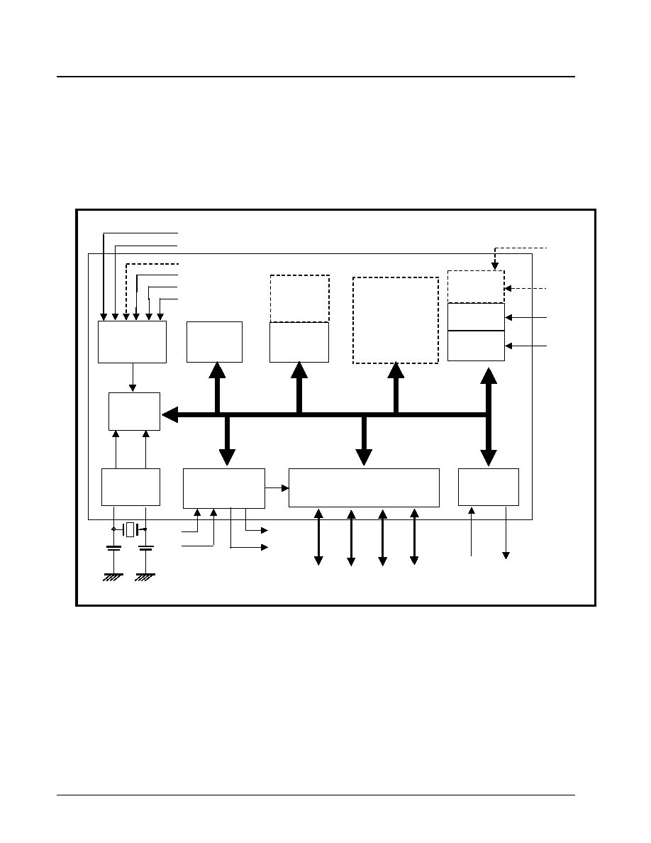
XRT7245
DS3 UNI FOR ATM
·Á
·Á
·Á
·Á
PRELIMINARY
REV. 1.03
124
The 8051 Microcontroller
The 8051 family of microcontrollers is manufactured
by Intel and comes with a variety of amenities. Some
of these amenities include:
∑
on chip serial port
∑
four 8 bit I/O port (P0≠P3)
∑
two 16 bit timers
∑
4k bytes of ROM
∑ 128 bytes of RAM
Figure 20 presents a block diagram of the 8051 Mi-
crocontroller, and Figure 2 presents the pin out of this
device.
The 8051 µC consists of 4 8-bit I/O ports. Some of
these ports have alternate functions as will be dis-
cussed below.
Port 0 (P0.0≠P0.7)
This port is a dual purpose port on pins 32≠39 of the
8051 IC. In minimal component designs, it is used as
a general purpose I/O port. For larger designs with
external memory, it becomes a multiplexed address
and data bus (AD0≠AD7).
Port 1 (P1.0≠P1.7)
Port 1 is a dedicated port on pins 1≠8. The pins,
designated at P1.0, P1.1, P1.2,..., are available for in-
terfacing as required. No alternative functions are as-
signed for Port 1 pins; thus they are used solely
for interfacing external devices. Exceptions are the
8032/8052 ICs, which use P1.0 and P1.1 either as I/O
lines or as external inputs to the third timer.
F
IGURE
20. B
LOCK
D
IAGRAM
OF
THE
8051 M
ICROCONTROLLER
Interrupt
Control
Other
Registers
128 bytes
RAM
(8032/8052)
128 bytes
RAM
ROM
0K - 8031/8032
4K - 8051
8K - 8052
Timer 2
(8032/8052)
Timer 1
Timer 0
CPU
Bus Control
I/O Ports
Serial Port
RXD*
TXD*
P
0
P
1
P2
P3
Serial Port
Timer 0
Timer 1
Timer 2 (8032/8052)
INT0*
INT1*
Oscillator
T2EX*
T2*
T1*
T0*
EA*
RST
ALE
PSEN*

·Á
·Á
·Á
·Á
DS3 UNI FOR ATM
XRT7245
PRELIMINARY
REV. 1.03
125
Port 2 (P2.0≠P2.7)
Port 2 (Pins 21
≠
28) is a dual-purpose port that can
function as general purpose I/O, or as the high byte
of the address bus for designs with external code
memory of more than 256 bytes of external data
memory (A8≠A15).
Port 3
Port 3 is a dual purpose port on pins 10≠17. In addi-
tion to functioning as general purpose I/O, these pins
have multiple functions. Each of these pins have an
alternate purpose, as listed in Table 8, below.
The 8051 also has numerous additional pins which
are relevant to interfacing to the XRT7245 DS3 UNI
or other peripherals. These pins are:
ALE--Address Latch Enable
If Port 0 is used in its alternate mode--as the data
bus and the lower byte of the address bus--ALE is
the signal that latches the address into an external
register during the first half of a memory cycle. Once
this is done Port 0 lines are then available for data in-
put or output during the second half of the memory
cycle, when the data transfer takes place.
INT0* (P3.2) and INT1* (P3.3)
INT0* and INT1* are external interrupt request inputs
to the 8051 µC. Each of these interrupt pins support
"direct interrupt" processing. In this case, the term
"direct" means that if one of these inputs are assert-
ed, then program control will automatically branch to a
specific (fixed) location in code memory. This location
is determined by the circuit design of the 8051 µC IC
and cannot be changed. Table 9 presents the loca-
tion (in code memory) where the program control will
branch to, if either of these inputs are asserted.
Therefore, if the user is using either one of these inputs
as an interrupt request input, then the user must insure
that the appropriate interrupt service routine or un-
conditional branch instruction (to the interrupt service
routine) is located at one of these address locations.
If the 8051 µC is required to interface to external
components in the data memory space of sizes
greater than 256 bytes, then both Port 0 and Port 2
must be used as the address and data lines. Port 0
will function as a multiplexed address/data bus. During
the first half of a memory cycle, Port 0 will operate as
the lower address byte. During the second half of the
memory cycle, Port 0 will operate as the bi-directional
data bus. Port 2 will be used as the upper address
byte. ALE and the use of a 74HC373 transparent
latch device can be used to demultiplex the Address
and Data bus signals.
Figure 21 presents a schematic illustrating how the
XRT7245 DS3 UNI can be interfaced to the 8051 µC.
T
ABLE
8: A
LTERNATE
F
UNCTIONS
OF
P
ORT
3 P
INS
B
IT
N
AME
A
LTERNATE
F
UNCTION
P3.0
RXD
Receive Data for Serial Port
P3.1
TXD
Transmit Data for Serial Port
P3.2
INT0*
External Interrupt 0
P3.3
INT1*
External Interrupt 1
P3.4
T0
Timer/Counter 0 External Input
P3.5
T1
Timer/Counter 1 External Input
P3.6
WR*
External Data Memory Write Strobe
P3.7
RD*
External Data Memory Read Strobe
T
ABLE
9: I
NTERRUPT
S
ERVICE
R
OUTINE
L
OCATIONS
(
IN
C
ODE
M
EMORY
)
FOR
INT0*
AND
INT1*
I
NTERRUPT
L
OCATION
INT0*
0003H
INT1*
0013H
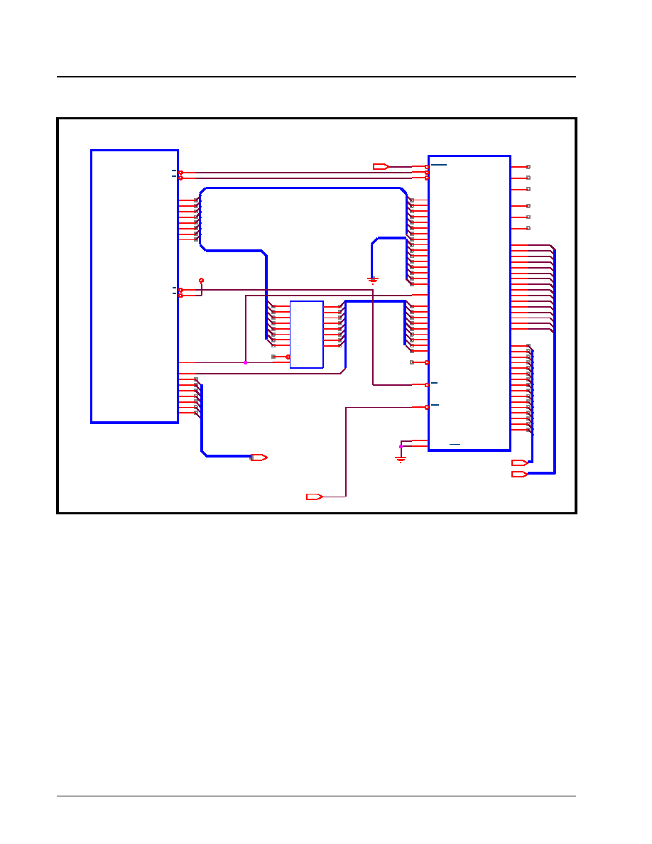
XRT7245
DS3 UNI FOR ATM
·Á
·Á
·Á
·Á
PRELIMINARY
REV. 1.03
126
The circuitry in Figure 21 will function as follows during
a UNI requested interrupt. The UNI device would re-
quest an interrupt from the CPU by asserting its ac-
tive low INT* output pin. This will cause the INT0* in-
put pin of the CPU to go "low". When this happens
the 8051 CPU will finish executing its current instruc-
tion, and will then branch program control the UNI in-
terrupt service routine. In the case of Figure 21, the
interrupt service routine will be located in 0003H in
code memory. The 8051 CPU does not issue an In-
terrupt Acknowledge signal back to the UNI. It will
just begin processing through the UNI's interrupt ser-
vice routine. Once the CPU has eliminated the
cause(s) of the interrupt request, the UNI's INT* pin
will be negated (go "high") and the CPU will return
from the interrupt service routine and resume normal
operation.
3.8
Interfacing the UNI to a Motorola type
Microprocessor
This section discusses how to interface the XRT7245
DS3 UNI to the 68000 microprocessor.
Figure 22 presents a schematic on how to interface the
XRT7245 DS3 UNI to the MC68000 microprocessor,
over a 16 bit data bus.
F
IGURE
21. S
CHEMATIC
D
EPICTING
HOW
TO
I
NTERFACE
THE
XRT7245 DS3 UNI
TO
THE
8051 M
ICROCONTROLLER
5V
A[8:0]
D[15:8]
D[7:0]
AD[7:0]
A[15:9]
R
x
D
a
t
a
[
1
5
:
0
]
T
x
D
a
t
a
[
1
5
:
0
]
U3
74HC 373
D0
3
D1
4
D2
7
D3
8
D4
13
D5
14
D6
17
D7
18
OC
1
G
11
Q0
2
Q1
5
Q2
6
Q3
9
Q4
12
Q5
15
Q6
16
Q7
19
U1
XR-T7245
TxNEG
111
TxPOS
109
TxLineClk
112
RxLineC lk
99
RxNEG
98
RxPOS
97
D15
1
D14
3
D13
4
D12
5
D11
9
D10
11
D9
13
D8
14
D7
16
D6
17
D5
18
D4
19
D3
21
D2
23
D1
25
D0
28
A8
37
A7
40
A6
41
A5
42
A4
43
A3
44
A2
45
A1
46
A0
48
TxData15
144
TxData14
142
TxData13
140
TxData12
138
TxData11
134
TxData10
132
TxData9
130
TxData8
128
TxData7
143
TxData6
141
TxData5
139
TxData4
137
TxData3
135
TxData2
133
TxData1
131
TxData0
129
M OTO/Intel
7
Rx Data0
70
Rx Data1
68
Rx Data2
64
Rx Data3
62
Rx Data4
60
Rx Data5
58
Rx Data6
56
Rx Data7
54
Rx Data8
69
Rx Data9
67
RxData10
65
RxData11
63
RxData12
61
RxData13
57
RxData14
55
RxData15
53
Reset
Rdy_Dtck
160
W idth16
20
W RB_RW
35
RDS_DS
33
ALE_AS
34
I nt
29
C S
32
U2
8051
W R
16
RD
17
AD0
39
AD1
38
AD2
37
AD3
36
AD4
35
AD5
34
AD6
33
AD7
32
ALE
30
A8
21
A9
22
A10
23
A11
24
A12
25
A13
26
A14
27
A15
28
INT0
12
INT1
13
To Address Decoder
From Address Dec oder
RESET Command Circuitry
RxData[15:0]
TxData[15:0]
·Á
·Á
·Á
·Á
DS3 UNI FOR ATM
XRT7245
PRELIMINARY
REV. 1.03
127
In general, the approach to interfacing these two
devices is pretty straightforward. However, the user
must be aware of the fact that the XRT7245 DS3 UNI
does not provide an interrupt vector to the MC68000,
during an "Interrupt Acknowledge" Cycle. Therefore,
the user must configure his/her design to support
"auto-vectored" interrupts. Auto-vectored interrupt
processing is a feature offered by the MC68000 Family
of microprocessors, where, if the microprocessor
knows (prior to any IACK cycle) the "Interrupt Level"
of this current interrupt, and that the "interrupting"
peripheral does not support vectored interrupts, then
the µP will generate its own Interrupt Vector. The
schematic shown in Figure 22, has been configured
to support auto-vectored interrupts.
Functional Description of Circuit in Figure 22.
When the XRT7245 DS3 UNI generates an interrupt,
the Int* output will toggle low. This will force Input 6,
of the "Interrupt Priority Encoder" chip (U4), to also
toggle low. In response to this, the Interrupt Priority
Encoder chip will set its three outputs to the following
states: A2 = `0', A1 = `0' and A0 = `1' (which is the
number 6 in "inverted" binary format). The state of three
output pins will be read by the active-low interrupt re-
quest inputs of the µP (IPL2, IPL1, and IPL0). When
the 68000 µP detects this value at its three interrupt
request inputs, it will know two things:
1.
An interrupt request has been issued by one of
the peripheral devices
2.
The interrupt request is a "Level 6" interrupt
request (due to the values of the A2≠A0 outputs
from the "Interrupt Priority Encoder" IC).
Once the 68000 µP has determined these two things
it will initiate an "Interrupt Acknowledge" (IACK) cycle
by doing the following:
1.
Identify this new bus cycle as an interrupt service
routine by setting all of its Function Code output
pins (FC2≠FC0) "high".
F
IGURE
22. S
CHEMATIC
D
EPICTING
HOW
TO
I
NTERFACE
THE
XRT7245 DS3 UNI
TO
THE
MC68000 M
ICROPROCESSOR
.
+5V
5V
5V
D[15:0]
D[15:0]
D[15:0]
A[23:10]
RxData[15:0]
TxData[15:0]
A[3:1]
A[8:0]
A[8:0]
A[9:1]
U1
XR-T7245
TxNEG
111
TxPOS
109
TxLineClk
112
RxLineClk
99
RxNEG
98
RxPOS
97
D15
1
D14
3
D13
4
D12
5
D11
9
D10
11
D9
13
D8
14
D7
16
D6
17
D5
18
D4
19
D3
21
D2
23
D1
25
D0
28
A8
37
A7
40
A6
41
A5
42
A4
43
A3
44
A2
45
A1
46
A0
48
TxData15
144
TxData14
142
TxData13
140
TxData12
138
TxData11
134
TxData10
132
TxData9
130
TxData8
128
TxData7
143
TxData6
141
TxData5
139
TxData4
137
TxData3
135
TxData2
133
TxData1
131
TxData0
129
MOTO/Intel
7
RxData0
70
RxData1
68
RxData2
64
RxData3
62
RxData4
60
RxData5
58
RxData6
56
RxData7
54
RxData8
69
RxData9
67
RxData10
65
RxData11
63
RxData12
61
RxData13
57
RxData14
55
RxData15
53
Reset
155
Rdy_Dtck
160
Width16
20
WRB_RW
35
RDS_DS
33
ALE_AS
34
Int
29
CS
32
U2
MC68000
RESET
18
R/W
9
DTACK
10
D0
5
D1
4
D2
3
D3
2
D4
1
D5
64
D6
63
D7
62
D8
61
D9
60
D10
59
D11
58
D12
57
D13
56
D14
55
D15
54
A1
29
A2
30
A3
31
A4
32
A5
33
A6
34
A7
35
A8
36
A9
37
FC0
28
FC1
27
FC2
26
VPA
21
IPL0
25
IPL1
24
IPL2
23
AS
6
UDS
7
LDS
8
A10
38
A11
39
A12
40
A13
41
A14
42
A15
43
A16
44
A17
45
A18
46
A19
47
A20
48
A21
49
A22
50
A23
51
U5
74AHCT138
A
1
B
2
C
3
G1
6
G2A
4
G2B
5
Y0
15
Y1
14
Y2
13
Y3
12
Y4
11
Y5
10
Y6
9
Y7
7
U3
74AHCT138
A
1
B
2
C
3
G1
6
G2A
4
G2B
5
Y0
15
Y1
14
Y2
13
Y3
12
Y4
11
Y5
10
Y6
9
Y7
7
U4
74AHCT148
0
10
1
11
2
12
3
13
4
1
5
2
6
3
7
4
EI
5
A0
9
A1
7
A2
6
GS
14
EO
15
U6A
74AHCT00
1
2
3
U7A
74AHCT04
1
2
U7B
74AHCT04
3
4
Address Decoder
Address Decoder
RxData[15:0]
TxData[15:0]

XRT7245
DS3 UNI FOR ATM
·Á
·Á
·Á
·Á
PRELIMINARY
REV. 1.03
128
2.
Placing the Interrupt Level on the Address output
pins A[3:1].
When the 68000 µP has toggled all of its Function
Code output pins "high", the "Function Code Decoder"
chip (U3) will read this value from the FC2≠FC0 pins
as being the binary value for 7. As result, U3 will
assert its active-low Y7 output pin. At the same time,
the address lines A[3:1] are carrying the current
"Interrupt Level" of this IACK cycle (level = 6, or `1 1 0'
in this example) and applying this value to the A, B,
and C inputs of the "IACK Level Decoder" chip (U5).
Initially, all of the outputs of U5 are tri-stated. Due to
the fact that its active-low G2A and G2B inputs are
negated (e.g., at a logic "high"). However, when the
68000 µP begins the IACK cycle, it will assert its
Address Strobe (AS*) signal. This action will result in
asserting the G2A input pin of U5. Additionally, since
the Function Code Decoder chip has also asserted
its Y7 output pin this will, in turn assert the G2B input
pin of U5. At this point, the output of U5 will no longer
be tri-stated. U5 will read in the contents of its A, B,
and C inputs, and assert the appropriate output pin.
In this case, since U5 has the binary value of "6"
applied to its input, it will, in turn assert its active-low
Y6 output pin. The combination of the Int* output (of
the XRT7245) and Y6 (from U5) being asserted will
cause U6A to assert the active-low VPA* (Valid
Peripheral Address) input pin of the 68000 µP. Any-
time the 68000 detects its VPA* pin being asserting
during an IACK cycle, it knows that this is an Auto-
vectored Interrupt Cycle. When the 68000 is operating
in an Auto-vectored Interrupt Cycle, it knows that it
will not receive an interrupt vector from the peripheral
device (e.g., the XRT7245 UNI in this case), and that
it must generate its own vector. In the very next bus
cycle, the 68000 µP is going to implement a "pseudo-
read" of the data bus. However, in reality no data will
be read from the XRT7245 device. The 68000 µP will
instead have determined that since this current IACK
is an Auto-vectored--Level 6 Interrupt cycle, which
corresponds to Vector Number 30, within the 68000
µP's Exception Vector Table, Vector Number 30 cor-
responds to an Address Space of 78h, in the 68000
µP's address space. In the case of this example, the
user is required to place an unconditional branch
statement (to the location of the XRT7245 Interrupt
Service Routine) at 78h in system level memory.
Table 10 presents the Auto-vector Table (e.g., the
relationship between the Interrupt Level and the
corresponding location in memory for this uncondi-
tional branch statement) for the MC68000 µP.
T
ABLE
10: A
UTO
-
VECTOR
T
ABLE
FOR
THE
MC68000 M
ICROPROCESSOR
I
NTERRUPT
L
EVEL
V
ECTOR
N
UMBER
A
DDRESS
S
PACE
1
25
064h
2
26
068h
3
27
06Ch
4
28
070h
5
29
074h
6
30
078h
7
31
07Ch

·Á
·Á
·Á
·Á
DS3 UNI FOR ATM
XRT7245
PRELIMINARY
REV. 1.03
129
4.0 THE UNI TEST AND DIAGNOSTIC
SECTION
The "Test and Diagnostic" Section, within the
XRT7245 DS3 UNI offers a significant amount of on-
chip "self-test" capability. This "self-test" capability of
the XRT7245 DS3 UNI is briefly itemized below.
∑
The XRT7245 DS3 UNI can be configured to oper-
ate in one of three loopback modes: Line, PLCP,
and Cell.
∑
The UNI contains an on-chip Test Cell Generator
that is capable of generating Test Cells with "user-
specified" header byte patterns. The Test Cell
Generator also uses an "on-chip" PRBS generator
to fill in the bytes for the payload portion of these
test cells.
∑
The "Test and Diagnostic" section, within the UNI
allows the user to route these test cells through the
UNI, while operating in the Line, PLCP, and a
"system level" external loopback mode.
∑
The Test and Diagnostic section includes a Test Cell
Receiver that is capable of identifying, terminating,
and evaluating the "post-loopback" test cells.
∑ The Test Cell Receiver will also report the occurrence
of errors, by incrementing an on-chip "Test Cell Error
Accumulation" register.
The UNI chip's Test and Diagnostic Section allows the
user to run a wide variety of diagnostic tests, based up-
on his/her selection of the following three parameters:
∑
The type of Loopback modes
∑
Line Side or System Side Testing
∑ Test Cell Generator/Receiver configuring
Each of these "Test and Diagnostic" parameters are
discussed in detail, below.
4.1
The UNI Chip's Loopback Modes
The XRT7245 DS3 UNI IC allows the user to configure
it into one of three loopback modes:
∑
Line Loopback Mode
∑
PLCP Loopback Mode
∑ Cell Loopback Mode
The following sections define each of these loopback
modes, and discusses how to configure the UNI to
operate in these modes.
4.1.1
The "Line Loopback" Mode
When the UNI is operating in the Line Loopback
Mode, the output of the Transmit DS3 Framer (e.g.,
TxPOS and TxNEG) will be internally routed to the
input pins of the Receive DS3 Framer (e.g., RxPOS
and RxNEG). Figure 23 presents an illustration of the
UNI chip operating in the Line Loopback mode.
F
IGURE
23. I
LLUSTRATION
OF
THE
UNI
OPERATING
IN
THE
L
INE
L
OOPBACK
M
ODE
.
UNI Chip
Tx
Utopia
Tx PLCP
Processor
Tx DS3
Framer
Rx DS3
Framer
Rx PLCP
Processor
Rx
Utopia
Tx Cell
Processor
Rx Cell
Processor
Line Loopback
XRT7245
DS3 UNI FOR ATM
·Á
·Á
·Á
·Á
PRELIMINARY
REV. 1.03
130
The user can configure the UNI chip to operate in the
Line Loopback mode, by writing the appropriate data
to the UNI Operating Mode Register (Address = 00h),
as depicted below.
Writing a "1" to bit 7 of the UNI Operating Mode Reg-
ister, configures the UNI to operate in the "Line Loop-
back" mode. Writing a "0" to this bit-field disables the
Line Loopback mode.
4.1.2
The PLCP Loopback Mode
When the UNI chip is configured to operate in the
"PLCP Loopback" mode, the PLCP frames, that have
been generated by the Transmit PLCP Processor, will
be routed directly (internally) to the Receive PLCP
Processor. Figure 24 presents an illustration of the
UNI chip operating in the PLCP Loopback mode.
The user can configure the UNI chip to operate in the
"PLCP Loopback" mode, by writing the appropriate
data to the UNI Operating Mode Register (Address =
00h), as depicted below.
Writing a "1" to bit 5 of the UNI Operating Mode Reg-
ister, configures the UNI to operate in the PLCP
Loopback mode. Writing a "0" to this bit-field disables
the PLCP Loopback mode.
4.1.3
The Cell Loopback Mode
When the UNI is configured to operate in the "Cell
Loopback" Mode, then ATM cells that are delineated
and pass through the Receive Cell Processor will be
UNI Operating Mode Register (Address = 00h)
B
IT
7
B
IT
6
B
IT
5
B
IT
4
B
IT
3
B
IT
2
B
IT
1
B
IT
0
Line Loopback
Cell Loopback
PLCP Loopback
Reset
Direct-Mapped ATM
C-Bit/M13
TimRefSel[1, 0]
R/W
R/W
R/W
R/W
R/W
R/W
R/W
R/W
F
IGURE
24. A
N
I
LLUSTRATION
OF
THE
UNI
CHIP
OPERATING
IN
THE
PLCP L
OOPBACK
M
ODE
.
UNI Chip
Tx
Utopia
Tx PLCP
Processor
Tx DS3
Framer
Rx DS3
Framer
Rx PLCP
Processor
Rx
Utopia
Tx Cell
Processor
Rx Cell
Processor
PLCP Loopback
UNI Operating Mode Register (Address = 00h)
B
IT
7
B
IT
6
B
IT
5
B
IT
4
B
IT
3
B
IT
2
B
IT
1
B
IT
0
Line Loopback
Cell Loopback
PLCP Loopback
Reset
Direct-Mapped ATM
C-Bit/M13
TimRefSel[1, 0]
R/W
R/W
R/W
R/W
R/W
R/W
R/W
R/W

·Á
·Á
·Á
·Á
DS3 UNI FOR ATM
XRT7245
PRELIMINARY
REV. 1.03
131
routed directly (internally) to the Tx FIFO (within the
Transmit UTOPIA Interface block). Once these cells
arrive at the TxFIFO, they will be read-in and further
processed by the Transmit Cell Processor. These
cells will ultimately be routed onto the "outbound" DS3
line via the Transmit DS3 Framer. Figure 25 presents
an illustration of the UNI chip operating in the "Cell
Loopback" Mode.
The user can configure the UNI chip to operate in the
"Cell Loopback" mode, by writing the appropriate data
to the UNI Operating Mode Register (Address = 00h),
as depicted below.
Writing a "1" to bit 6 of the UNI Operating Mode Reg-
ister configures the UNI to operate in the "Cell Loop-
back" mode. Writing a "0" to this bit-field disables the
"Cell Loopback" mode.
4.2
Line-Side/System-Side Tests
The current version of the XRT7245 DS3 UNI chip
supports "Line-Side" Testing, but not "System-Side"
testing. However, for the sake of completeness, both
of these test modes are briefly discussed below.
Future versions of the UNI Chip will allow the user to
generate test cells and run tests in either the "Line
Side" Mode or in the "System Side" Mode. The user
will be able to specify which of these mode he/she
wishes to run these tests in by writing the appropriate
value to Bit 2 (Line/System) of the "Test Cell Control
and Status" Register; as depicted below.
F
IGURE
25. A
N
I
LLUSTRATION
OF
THE
UNI
CHIP
OPERATING
IN
C
ELL
L
OOPBACK
M
ODE
.
UNI Chip
Tx
Utopia
Tx PLCP
Processor
Tx DS3
Framer
Rx DS3
Framer
Rx PLCP
Processor
Rx
Utopia
Tx Cell
Processor
Rx Cell
Processor
Cell Loopback
UNI Operating Mode Register (Address = 00h)
B
IT
7
B
IT
6
B
IT
5
B
IT
4
B
IT
3
B
IT
2
B
IT
1
B
IT
0
Line Loopback
Cell Loopback
PLCP Loopback
Reset
Direct-Mapped ATM
C-Bit/ M13
TimRefSel[1, 0]
R/W
R/W
R/W
R/W
R/W
R/W
R/W
R/W
Test Cell Control and Status Register (Address = 06h)
B
IT
7
B
IT
6
B
IT
5
B
IT
4
B
IT
3
B
IT
2
B
IT
1
B
IT
0
Unused
Test Cell Enable
Line/System
One Shot Test
One Shot Done
PRBS Lock
R/W
R/W
R/W
R/W
R/W
R/W
RO
RO

XRT7245
DS3 UNI FOR ATM
·Á
·Á
·Á
·Á
PRELIMINARY
REV. 1.03
132
Writing a "0" into this bit-field configures the UNI to
support "Line Side" Tests. Writing a "1" into this bit-
field presently does nothing. Currently, this version of
the XRT7245 DS3 UNI does not support the "System
Side" Test Mode.
A description for each of these Test Modes (including
the System-side Test Mode) is presented below.
4.2.1
Line-Side Tests
In "Line Side" Testing, the UNI chip will generate
some test cells, and will transmit these cells either on
or out towards the DS3 "Line" (hence the name "Line-
side" tests). At some point, these test cells will be
looped-back into the Receive Path, where they will
ultimately be terminated, and evaluated by the Test
Cell Receiver. These Line-Side tests are intended to
be conducted while the UNI is operating in the "Line-"
or "PLCP--" loopback modes (see Section 4.1). How-
ever, the Line Side tests can also be conducted while
the system (external to the UNI device), implements
an "External Loopback" mode. In this case, no UNI
loopback mode would be configured, and the user's
system would implement this "External Loopback" by
routing the "Transmit DS3 Line data" (from the UNI),
back into the RxPOS and RxNEG inputs of the UNI
device.
Note: The Cell Loopback Mode cannot be used in the
"Line-Side" Tests.
If the user selects a "Line Side" test, then the "Test
Cell Generator" will generate and insert test cells into
the TxFIFO (within the UNI). These test cells will be
read out of the TxFIFO by the Transmit Cell Processor,
and are ultimately transmitted out onto the DS3 line.
Eventually (depending upon the type of Loopback
chosen), these test cells will be routed back into the
"Receive Path" of the UNI device. Once in the "Receive
Path", those test cells that reach the RxFIFO will be
identified by their header byte patterns, and collected
by the "Test Cell Receiver" where they will be checked
for bit errors. The features and characteristics of the
Test Cell Generator and the Test Cell Receiver is
discussed in detail in Section 4.3.
The configuration for the Line-side Test, while the
UNI is configured to operate in the PLCP, Line and
"External" Loopback modes are illustrated in Figure 26
through 28, respectively.
F
IGURE
26. I
LLUSTRATION
OF
L
INE
S
IDE
T
EST
,
WHILE
THE
UNI
IS
CONFIGURED
TO
OPERATE
IN
THE
PLCP
L
OOPBACK
M
ODE
UNI Chip
Tx Utopia
Tx PLCP
Processor
Tx DS3
Framer
Rx DS3
Framer
Rx PLCP
Processor
Rx Utopia
Tx Cell
Processor
Rx Cell
Processor
PLCP Loopback
Test Cell
Generator
Test Cell
Receiver
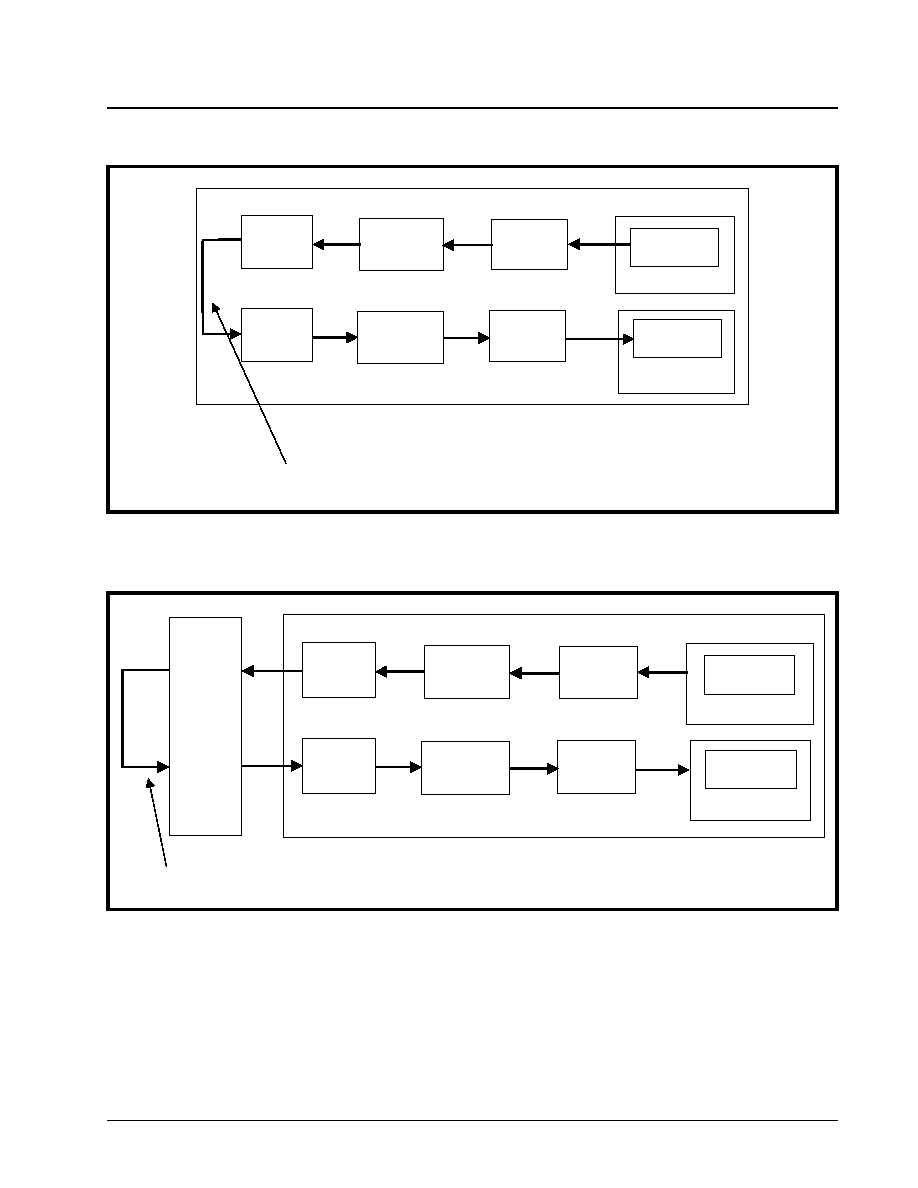
·Á
·Á
·Á
·Á
DS3 UNI FOR ATM
XRT7245
PRELIMINARY
REV. 1.03
133
4.2.2
"System Side" Testing (Not Presently
Supported by the XRT7245 DS3 UNI)
If the user selects a "System side" test then the "Test
Cell Generator" will generate and insert the test cells
into the RxFIFO, where they can be read out and pro-
cessed by the ATM Layer processor, via the Receive
UTOPIA Interface block. At some point, these test
cells will be looped back into the "Transmit Path" (of
the UNI device), via some externally implemented
"UTOPIA Loopback" mode. Once in the "transmit
path", those test cells that reach the TxFIFO (of the
UNI) will be identified by their header byte patterns,
and collected by the "Test Cell Receiver" where they
will be checked for bit errors. Figure 29 presents an il-
lustration of a System Side Test Configuration, while
the UNI System is operating in a "UTOPIA Loopback
Mode", via the ATM Layer Processor.
F
IGURE
27. I
LLUSTRATION
OF
L
INE
S
IDE
T
EST
,
WHILE
THE
UNI
IS
CONFIGURED
TO
OPERATE
IN
L
INE
L
OOPBACK
M
ODE
UNI Chip
Tx Utopia
Tx PLCP
Processor
Tx DS3
Framer
Rx DS3
Framer
Rx PLCP
Processor
Rx Utopia
Tx Cell
Processor
Rx Cell
Processor
Line Loopback
Test Cell
Generator
Test Cell
Receiver
F
IGURE
28. I
LLUSTRATION
OF
L
INE
S
IDE
T
EST
,
WHILE
THE
UNI
IS
CONFIGURED
TO
OPERATE
IN
THE
"E
XTERNAL
L
OOPBACK
M
ODE
."
UNI Chip
Tx Utopia
Tx PLCP
Processor
Tx DS3
Framer
Rx DS3
Framer
Rx PLCP
Processor
Rx Utopia
Tx Cell
Processor
Rx Cell
Processor
External Loopback
Test Cell
Generator
Test Cell
Receiver
LIU Chip
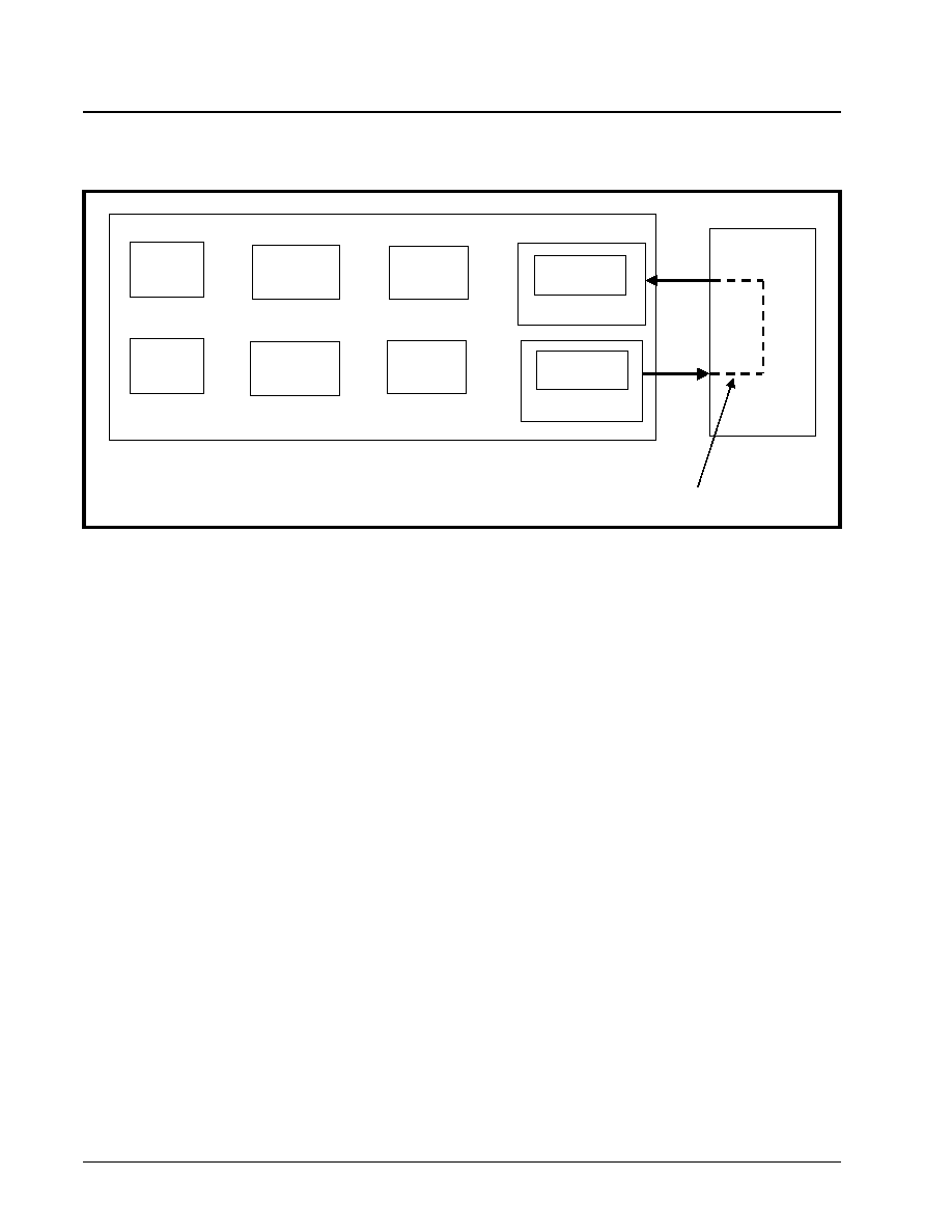
XRT7245
DS3 UNI FOR ATM
·Á
·Á
·Á
·Á
PRELIMINARY
REV. 1.03
134
Note:
1. The System-side test is not supported by this version
of the XRT7245 DS3 UNI IC.
2. The "UTOPIA Loopback" mode, as depicted in
Figure 29, must be implemented by the user's
system level hardware.
4.3
Operating the Test Cell Generator/Receiver
Sections 4.1 discussed the various loopback modes
that are available within the UNI device. Section 4.2
discussed Line Side Testing; where the "internal" Test
Cell Generator can be enabled to produce test cells,
and write them into the TxFIFO. These cells will be
read out of the TxFIFO by the Transmit Cell Processor,
and routed towards the DS3 line. Section 4.1 and 4.2
also mentioned that these cells could be "looped"
back into the Receive path (of the UNI), at various
points depending upon the Loopback Mode selected.
When operating the UNI in the Line Side Test Mode,
the following loopback options are available.
∑
PLCP Loopback
∑
Line Loopback
∑ External Loopback
As these test cells proceed through the Receive path
(after traversing the loopback point), they will eventu-
ally arrive at the RxFIFO (within the Receive UTOPIA
Interface); where they will be identified, collected and
analyzed by the Test Cell Receiver.
The next two sections discuss the operation of the
Test Cell Generator and the Test Cell Receiver, with
the UNI Test and Diagnostic Section.
4.3.1
Characteristics of the Test Cell Generator
The Test Cell Generator has the following
characteristics:
∑
It allows the user to specify the header byte patterns
of these test cells.
∑
The payload bytes within these test cells will be
filled by an internal Pseudo-Random Byte
Sequence (PRBS) Pattern Generator.
∑
It allows the user to select one of two "Test Cell
Traffic" generating options. These options are:
1.
The "One Shot" Mode
2.
The "Continuous" Mode
∑ It generates Test Cells and writes them into the
TxFIFO (within the Transmit UTOPIA Interface
block), where they will be read from and processed
throughout the UNI.
Each of these Characteristics of the Test Cell Gener-
ator are described in greater detail below.
4.3.1.1
Specifying the Header Byte Pattern of
Test Cells
The user can specify his/her choice for the header byte
patterns of these Test Cells, by writing the "desired"
header byte patterns into the "Test Cell Header Byte"
F
IGURE
29. I
LLUSTRATION
OF
S
YSTEM
S
IDE
T
EST
,
WHILE
THE
UNI S
YSTEM
IS
CONFIGURED
TO
OPERATING
IN
UTOPIA L
OOPBACK
M
ODE
.
Utopia Loopback
UNI Chip
Tx Utopia
Tx PLCP
Processor
Tx DS3
Framer
Rx DS3
Framer
Rx PLCP
Processor
Rx Utopia
Tx Cell
Processor
Rx Cell
Processor
Test Cell
Receiver
Test Cell
Generator
ATM Layer
Processor

·Á
·Á
·Á
·Á
DS3 UNI FOR ATM
XRT7245
PRELIMINARY
REV. 1.03
135
registers 1 through 4 (Address = 08h through 0Bh); as
depicted below.
Writing the Test Cell Header bytes into these registers
accomplishes two things:
a.
It configures the Test Cell Generator to
produce Test Cells with these header byte
patterns; and
b.
It informs the Test Cell Receiver of the
"header bytes" patterns of these Test Cells,
in order to help it to identify and collect these
cells for error-checking purposes.
4.3.1.2
The Payload Bytes of the Test Cells
The Test Cell Generator will automatically fill the
payload portion of these Test Cells with bytes that
are generated by an internal Pseudo-Random Byte
Sequence (PRBS) generator. These PRBS generated
bytes will ultimately be used by the Test Cell Receiver
in order to perform error-checking of the "post-routed"
Test Cells.
4.3.1.3
Test Cell Generator--Test Cell Traffic
Options
The user can configure the Test Cell Generator to
generate "Test Cells" based upon one of two traffic
options: The "One Shot" Mode, or the "Continuous"
Mode. The user can make this selection by writing
the appropriate value to Bit 2 of the Test Cell Control
and Status Register (Address = 06h); as depicted
below.
Test Cell Header Byte-1 Register (Address = 08h)
B
IT
7
B
IT
6
B
IT
5
B
IT
4
B
IT
3
B
IT
2
B
IT
1
B
IT
0
Test Cell Header Byte 1
R/W
R/W
R/W
R/W
R/W
R/W
R/W
R/W
0
0
0
0
0
0
0
0
Test Cell Header Byte-2 Register (Address = 09h)
B
IT
7
B
IT
6
B
IT
5
B
IT
4
B
IT
3
B
IT
2
B
IT
1
B
IT
0
Test Cell Header Byte 2
R/W
R/W
R/W
R/W
R/W
R/W
R/W
R/W
0
0
0
0
0
0
0
0
Test Cell Header Byte-3 Register (Address = 0Ah)
B
IT
7
B
IT
6
B
IT
5
B
IT
4
B
IT
3
B
IT
2
B
IT
1
B
IT
0
Test Cell Header Byte 3
R/W
R/W
R/W
R/W
R/W
R/W
R/W
R/W
0
0
0
0
0
0
0
0
Test Cell Header Byte-4 Register (Address = 0Bh)
B
IT
7
B
IT
6
B
IT
5
B
IT
4
B
IT
3
B
IT
2
B
IT
1
B
IT
0
Test Cell Header Byte 4
R/W
R/W
R/W
R/W
R/W
R/W
R/W
R/W
0
0
0
0
0
0
0
0
XRT7245
DS3 UNI FOR ATM
·Á
·Á
·Á
·Á
PRELIMINARY
REV. 1.03
136
The user can configure the "Test Cell Generator" to
operate in the "One Shot" mode by writing a "1" into
this bit-field. Conversely, the user can configure the
"Test Cell Generator" to operate in the "Continuous"
Mode by writing a "0" into this bit-field.
4.3.1.3.1
The "One Shot" Mode
If the Test Cell Generator is configured to operate in
the "One Shot" mode, then upon enabling the Test Cell
Generator (by inducing a "0" to "1" transition in the
"Test Cell Enable" field of this register), the Test Cell
Generator will generate a "single burst" of 1024 test
cells. Afterward, the Test Cell Generator will stop and
will not produce any more test cells until the next "0"
to "1" transition in the "Test Cell Enable" bit-field.
If the Test Cell Generator is operating in the "One
Shot" Mode, the user can determine its "progress" in
its "Test Cell" production by reading Bit 1 (One Shot
Done) of the "Test Cell Control and Status Register";
as depicted below.
If this "Read-Only" bit-field contains a "1" then the
Test Cell Generator has completed its generation of
the latest burst of 1024 Test Cells. However, if this
bit-field contains a "0", then generation of this burst
of Test Cells is still in-process.
Note: The contents within Bit 1 (One Shot Done) is only
relevant if the user is operating the Test Cell Generator in
the "One Shot" Mode.
4.3.1.3.2
The "Continuous" Mode
If the Test Cell Generator is configured to operate in the
"Continuous" mode, then upon enabling the Test Cell
Generator (by writing a "1" into the "Test Cell Enable"
bit-field in this register), the Test Cell Generator will
produce a continuous stream of Test Cells for the
duration that the Test Cell Generator is enabled.
4.3.1.4
Enabling the "Test Cell Generator"
The user can Enable the "production" of Test Cells by
writing a "1" to Bit 4 (Test Cell Enable) of the Test Cell
Control and Status Register, as depicted below.
Writing a "1" to this bit-field enables the "Test Cell
Generator/Receiver". Writing a "0" disables the "Test
Cell Generator/Receiver".
Once the Test Cell Generator has been enabled, it
will begin to either produce a continuous stream of
cells (if configured to operate in the "Continuous"
mode), or a single burst of 1024 cells (if configured to
operate in the "One Shot" mode.)
4.3.2
Characteristics of the Test Cell Receiver
The Test Cell Receiver has the following characteris-
tics:
∑
It checks the header bytes of all cells arriving at the
RxFIFO (within the Receive UTOPIA Interface
Block), in order to determine if they are (or are not)
Test Cells.
Test Cell Control and Status Register (Address = 06h)
B
IT
7
B
IT
6
B
IT
5
B
IT
4
B
IT
3
B
IT
2
B
IT
1
B
IT
0
Unused
Test Cell Enable
Line/System
One Shot Test
One Shot Done
PRBS Lock
R/W
R/W
R/W
R/W
R/W
R/W
RO
RO
Test Cell Control and Status Register (Address = 06h)
B
IT
7
B
IT
6
B
IT
5
B
IT
4
B
IT
3
B
IT
2
B
IT
1
B
IT
0
Unused
Test Cell Enable
Line/System One Shot Test
One Shot Done
PRBS Lock
R/W
R/W
R/W
R/W
R/W
R/W
RO
RO
Test Cell Control and Status Register (Address = 06h)
Bit 7
Bit 6
Bit 5
Bit 4
Bit 3
Bit 2
Bit 1
Bit 0
Unused
Test Cell Enable
Line/System One Shot Test One Shot Done
PRBS Lock
R/W
R/W
R/W
R/W
R/W
R/W
RO
RO

·Á
·Á
·Á
·Á
DS3 UNI FOR ATM
XRT7245
PRELIMINARY
REV. 1.03
137
∑
It reads in those cells that have identified as "Test
Cells" from the RxFIFO
∑
Acquires and Maintains "PRBS Lock" with the pay-
load data, within these Test Cells.
∑
Reports the occurrences of errors.
4.3.2.1
Identifying the Test Cells
The Test Cell Receiver will monitor those cells that
reach the RxFIFO, within the Receive UTOPIA Inter-
face block, and, from that "stream of incoming cells"
identify and collect the test cells. The Test Cell
Receiver will use the "user-specified" header byte
patterns, as written into the "Test Cell Header Byte"
registers-1 through 4 (Address = 08h to 0Bh), in order
identify these test cells.
4.3.2.2
Acquiring and Maintaining "PRBS Lock"
During Test Cell production, the Test Cell Generator
will fill in the "payload portions" of each test cell with
bytes that were generated by a "Pseudo-Random
Byte Sequence (PRBS) generator. Consequently, the
contents within the cell payload bytes (of these test
cells) do follow a pre-defined sequence.
After the Test Cell Receiver has started to "collect"
these test cells from the RxFIFO, it will "strip off" the
cell header bytes and will begin to evaluate their pay-
load bytes. One of the first things that the Test Cell
Receiver will try to do is to look for this "pre-defined
(PRBS) sequence" within this test cell payload data.
Once the Test Cell Receiver has found this "pre-
defined" sequence within the test cell payload data,
it will inform the user of this fact by asserting the
"PRBS Lock" bit-field, within the "Test Cell Control
and Status" Register; as depicted below.
As long as the Test Cell Receiver has found (and
continues to find) this pre-defined sequence in the
incoming Test Cell payload data, it will keep this
bit-field asserted (e.g., at a logic "1").
4.3.2.3
Evaluating the Test Cell Payload Data
and Reporting Errors
Once the Test Cell Receiver has acquired "PRBS Lock"
with the contents of the incoming Test Cell payload
data; then it can begin to compare this data with the
"pre-defined" PRBS pattern of data, as produced by
the PRBS Generator (within the Test Cell Generator).
If the Test Cell Receiver detects any discrepancies
between the Test Cell Payload bytes, and the "pre-
defined" PRBS pattern, then it will increment to the
"Test Cell Error Accumulator" Registers. The "Test
Cell Error Accumulator" register actually consists of
two 8-bit "Reset upon Read" registers, as depicted
below.
Test Cell Control and Status Register (Address = 06h)
B
IT
7
B
IT
6
B
IT
5
B
IT
4
B
IT
3
B
IT
2
B
IT
1
B
IT
0
Unused
Test Cell Enable
Line/System
One Shot Test
One Shot Done
PRBS Lock
R/W
R/W
R/W
R/W
R/W
R/W
RO
RO
1
0
x
x
1
Test Cell Error Accumulator--MSB (Address = 0Ch)
B
IT
7
B
IT
6
B
IT
5
B
IT
4
B
IT
3
B
IT
2
B
IT
1
B
IT
0
Test Cell Errors--High Byte
RUR
RUR
RUR
RUR
RUR
RUR
RUR
RUR
Test Cell Error Accumulator--LSB (Address = 0Dh)
B
IT
7
B
IT
6
B
IT
5
B
IT
4
B
IT
3
B
IT
2
B
IT
1
B
IT
0
Test Cell Errors--Low Byte
RUR
RUR
RUR
RUR
RUR
RUR
RUR
RUR

XRT7245
DS3 UNI FOR ATM
·Á
·Á
·Á
·Á
PRELIMINARY
REV. 1.03
138
These two registers combine to form a 16-bit expres-
sion of the number of bit-errors that the Test Cell
Receiver has detected within the payload bytes of
the "incoming" test cells. The "Test Cell Error
Accumulator--MSB" register contains the "upper"
byte value of this 16-bit expression. Likewise, the
"Test Cell Error Accumulator--LSB" register contains
the "lower" byte value of this 16-bit expression.
Since these registers are "Reset upon Read", they
contain the number of "test cell payload" bit errors
that have been detected by the Test Cell Receiver
since the last read of these registers.
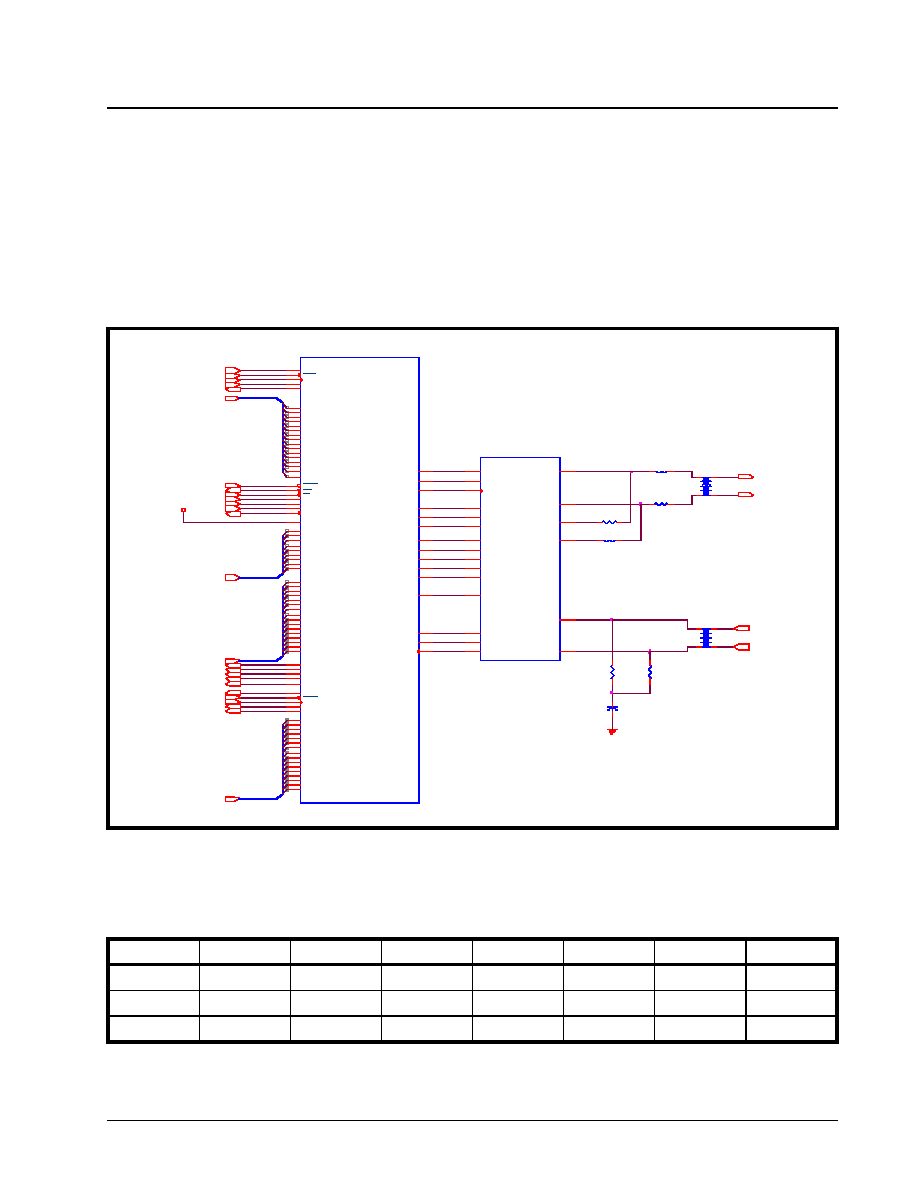
·Á
·Á
·Á
·Á
DS3 UNI FOR ATM
XRT7245
PRELIMINARY
REV. 1.03
139
5.0 LINE INTERFACE DRIVE
AND SCAN SECTION
The "Line Interface Drive and Scan" Section, of the
XRT7245 DS3 UNI consists of 5 output pins, three
input pins, a "Read/Write" register, and a "Read Only"
register.
The purpose of the "Line Interface Drive and Scan"
section, is to allow the user to monitor and exercise
control over many aspects of the XRT7300 DS3/E3
LIU IC without having to develop the necessary "off-
chip" glue logic.
Figure 30 presents a simply circuit schematic that
depicts how the XRT7245 DS3 UNI should be inter-
faced to the XRT7300 DS3/E3 LIU IC.
As mentioned above, the Line Interface Drive and
Scan Section, consists of five output pins and three
input pins. The logic state of the output pins are con-
trolled by the contents within the "Line Interface
Drive" Register, as depicted below.
F
IGURE
30. C
IRCUIT
S
CHEMATIC
I
LLUSTRATING
HOW
THE
XRT7245 DS3 UNI
SHOULD
BE
INTERFACED
TO
THE
XRT7295/XRT7296 DS3 L
INE
I
NTERFACE
U
NIT
DEVICES
.
+5V
Rx Data[15 :0]
D[15:0]
A[8:0]
T xDa ta[15 :0]
TxSoC
TxEnB*
TxClk
TxPrty
RESETB*
RW
DS
AS
RxClk
CS B*
RxEnB*
T xClav
INT*
DTACK*
RxLOS
RxOOF
RxLCD
RxRED
RxAIS
RxSOC
RxPr ty
RxClav
T T IP
T RING
RT IP
RRI NG
U1
XRT 73 00
T PDATA
37
T NDATA
38
T CLK
36
RCLK1
31
RNEG
32
RPOS
33
T T IP
41
TRING
40
MTIP
44
MRING
43
RRING
9
RT IP
8
DMO
4
RLOS
24
RLOL
23
L LB
14
RLB
15
T AOS
2
T xLEV
1
ENCODIS
21
REQDIS
12
T 1
1:1
1
5
4
8
T 2
1:1
1
5
4
8
U2
XRT 7245
T x POS
109
TxNE G
111
TxLineClk
112
DMO
6
ExtL OS
86
RLOL
8
LLOOP
28
RL OOP
26
T AOS
2
T xLEV
24
ENCODIS
22
REQB
12
Rx POS
97
RxNE G
98
RxLineClk
99
A0
48
A1
46
A2
45
A3
44
A4
43
A5
42
A6
41
A7
39
A8
37
D0
27
D1
25
D2
23
D3
21
D4
19
D5
18
D6
17
D7
16
D8
14
D9
13
D10
11
D11
9
D12
5
D13
4
D14
3
D15
1
RESET
1 55
INT
29
CS
32
WRB_RW
35
RDB_DS
33
ALE_AS
1 57
Rdy_Dtck
1 60
MOTO
7
RxLOS
88
RxOOF
90
RxLCD
30
RxRED
1 01
RxAIS
92
RxSOC
72
RxEnB
81
RxClk
50
RxPr ty
74
RxClav
76
TxSoC
1 24
TxEnB
1 23
TxClk
1 51
TxPrty
1 25
TxClav
1 26
RxData 0
70
RxData 1
68
RxData 2
64
RxData 3
62
RxData 4
60
RxData 5
58
RxData 6
56
RxData 7
54
RxData 8
69
RxData 9
67
RxData 10
65
RxData 11
63
RxData 12
61
RxData 13
57
RxData 14
55
RxData 15
53
TxData0
1 29
TxData1
1 30
TxData2
1 31
TxData3
1 32
TxData4
1 33
TxData5
1 34
TxData6
1 35
TxData7
1 36
TxData8
1 37
TxData9
1 38
TxData1 0
1 39
TxData1 1
1 40
TxData1 2
1 41
TxData1 3
1 42
TxData1 4
1 43
TxData1 5
1 44
R1
36
1
2
R4
2 70
1
2
R2
36
1
2
R3
2 70
1
2
R5
3 7.5
1
2
R6
37 .5
1
2
C1
0.01 uF
1
2
Line Interface Drive Register (Address = 72h)
B
IT
7
B
IT
6
B
IT
5
B
IT
4
B
IT
3
B
IT
2
B
IT
1
B
IT
0
Unused
REQB
TAOS
Encodis
TxLev
RLOOP
LLOOP
RO
RO
R/W
R/W
R/W
R/W
R/W
R/W
0
0
0
0
1
0
0
0

XRT7245
DS3 UNI FOR ATM
·Á
·Á
·Á
·Á
PRELIMINARY
REV. 1.03
140
The role of each of these bit-fields and their corre-
sponding output pins are depicted below.
The logic state of the input pins can be monitored by
reading the contents of the "Line Interface Scan"
Register, as depicted below.
Bit 5--REQB (Receive Equalization Enable/
Disable Select)
This "Read/Write" bit-field allows the user to control
the state of the "REQB" output pin of the UNI device.
This output pin is intended to be connected to the
"REQB" input pin of the XRT7300 DS3/E3 LIU IC. If
the user forces this signal to toggle "high", then the
internal Receive Equalizer (within the XRT7300 device)
will be disabled. Conversely, if the user forces this
signal to toggle "low", then the Receive Equalizer
(within the XRT7300 device) will be enabled.
The purpose of the internal Receive Equalizer (within
the XRT7300 device) is to compensate for the
"Frequency-Dependent" attenuation (e.g., cable-loss),
that a line signal will experience as it travels through
coaxial cable, from the transmitting to the receiving
terminal.
Writing a "1" to this bit-field causes the UNI device to
toggle the "REQB" output pin "high". Writing a "0" to
this bit-field causes the UNI device to toggle the
"REQB" output pin "low".
For information on the criteria that should be used
when deciding whether to enable or disable the
Receive Equalizer, please consult the XRT7300 device.
Note: If the customer is not using the XRT7300 DS3/E3/
STS-1 IC, then he/she can use this bit-field and the "REQB"
output pin for other purposes.
Bit 4--TAOS (Transmit All Ones Signal)
This "Read/Write" bit-field allows the user to control
the state of the "TAOS" output pin of the UNI device.
This output pin is intended to be connected to the
"TAOS" input pin of the XRT7300 DS3/E3/STS-1 LIU
IC. If the user forces this signal to toggle "high", then
the XRT7300 device will transmit an "All Ones" pat-
tern onto the line. Conversely, if the user commands
this output signal to toggle "low" then the XRT7300
DS3/E3/STS-1 LIU IC will proceed to transmit data
based upon the pattern that it receives via the TxPOS
and TxNEG output pins (of the UNI IC).
Writing a "1" to this bit-field will cause the "TAOS" out-
put pin to toggle "high". Writing a "0" to this bit-field
will cause this output pin to toggle "low".
Note: If the customer is not using the XRT7300 DS3/E3/
STS-1 LIU IC, then he/she can use this bit-field, and the
"TAOS" output pin for other purposes.
Bit 3--Encodis (B3ZS Encoder Disable)
This "Read/Write" bit-field allows the user to control
the state of the "Encodis" output pin of the UNI device.
This output pin is intended to be connected to the
"Encodis" input pin of the XRT7300 DS3/E3/STS-1
LIU IC. If the user forces this signal to toggle "high",
then the "internal B3ZS encoder" (within the XRT7300
device) will be disabled. Conversely, if the user com-
mand this output signal to toggle "low", then the
"internal B3ZS encoder" (within the XRT7300 device)
will be enabled.
Writing a "1" to this bit-field causes the UNI IC to
toggle the "Encodis" output pin "high". Writing a "0"
to this bit-field
Note:
1. The B3ZS encoder, within the XRT7300 device, is
not to be confused with the B3ZS encoding capa-
ble that exists within the Transmit DS3 Framer
block of the UNI IC.
2. The user is advised to disabled the B3ZS encoder
(within the XRT7300 IC) if the Transmit and
Receive DS3 Framers (within the UNI) are config-
ured to operate in the B3ZS line code.
3. If the customer is not using the XRT7300 DS3/E3/
STS-1 LIU IC, then he/she can use this bit-field
and the "Encodis" output pin for other purposes.
4. It is permissible to tie both the "Encodis" and
"Decodis" input pins (of the XRT7300 device) to the
"Encodis" output pin of the XRT7245 DS3 UNI.
Bit 2--TxLev (Transmit Line Build-Out Enable/
Disable Select)
This "Read/Write" bit-field allows the user to control
the state of the "TxLev" output pin of the UNI device.
This output pin is intended to be connected to the
"TxLev" input pin of the XRT7300 DS3/E3 LIU IC.
Writing a "1" to this bit-field commands the UNI to
toggle the TxLev output "high". Writing a "0" to this
bit-field commands the UNI to toggle this output
signal "low".
If the user commands this signal to toggle "high",
then the Transmit Line Build-Out circuitry, within the
XRT7300 device will be disabled. In this mode, the
XRT7300 LIU IC will generate unshaped (e.g., square)
pulses out onto the line, via the TTIP and TRING
output pins.
Conversely, if the user commands this signal to toggle
"low", then the Transmit Line Build-Out circuitry, within
the XRT7300 device will be enabled. In this mode,
XRT7300 LIU IC will generate shaped pulses out onto
the line, via the TTIP and TRING output pins.

·Á
·Á
·Á
·Á
DS3 UNI FOR ATM
XRT7245
PRELIMINARY
REV. 1.03
141
In order to comply with the "Isolated DSX-3 Pulse
Template" Requirements (per Bellcore GR-499-CORE),
the user is advised to set this bit-field to "0" if the
cable length (between the transmit output of the
XRT7300 device and the Digital Cross Connect
System) is less than 225 feet. Conversely, the user is
advised to set this bit-field to "1" if the cable length
(between the transmit output of the XRT7300 device
and the Digital Cross Connect System) is greater
than 225 feet.
Note: If the customer is not using the XRT7300 DS3/E3/
STS-1 IC, then he/she can use this bit-field and the TxLev
output pin for other purposes.
Bit 1--RLOOP (Remote Loop-back Select)
This "Read/Write" bit-field allows the user to control
the state of the "RLOOP" output pin of the UNI device.
This output pin is intended to be connected to the
"RLOOP" input pin of the XRT7300 DS3/E3/STS-1
LIU IC.
The state of this bit-field (or pin) along with "LLOOP"
are used to configure the XRT7300 device into one of
four (4) loop-back modes. The relationship of the values
of "RLOOP", "LLOOP" and the resulting loop-back
mode (within the XRT7300 device) is tabulated below .
Writing a "1" into this bit-field commands the UNI to
toggle the "RLOOP" output signal "high". Writing a
"0" into this bit-field commands the UNI to toggle this
output signal "low".
For a detailed description of the XRT7300 LIU's oper-
ation during each of these loop-back modes, please
see the "XRT7300 DS3/E3/STS-1 LIU IC" Data Sheet.
Note: If the customer is not using the XRT7300 DS3/E3/
STS-1 LIU IC, then he/she can use this bit-field and the
"RLOOP" output pin for other purposes.
Bit 0--LLOOP (Local Loop-back Select)
This "Read/Write" bit-field allows the user to control
the state of the "LLOOP" output pin of the UNI device.
This output pin is intended to be connected to the
"LLOOP" input pin of the XRT7300 DS3/E3/STS-1
LIU IC.
The state of this bit-field (or pin) along with "RLOOP"
are used to configure the XRT7300 device into one of
four (4) loop-back modes. The relationship of the values
of "RLOOP", "LLOOP" and the resulting loop-back
mode (within the XRT7300 device) is tabulated below.
Writing a "1" into this bit-field commands the UNI to
toggle the "LLOOP" output signal "high". Writing a "0"
into this bit-field commands the UNI to toggle this
output signal "low".
For a detailed description of the XRT7300 LIU's oper-
ation during each of these loop-back modes, please
see the "XRT7300 DS3/E3/STS-1 LIU IC" Data Sheet.
Note: If the customer is not using the XRT7300 DS3/E3/
STS-1 LIU IC, then he/she can use this bit-field and the
"LLOOP" output pin for other purposes.
RLOOP
LLOOP
R
ESULTING
L
OOP
-
BACK
M
ODE
(
WITHIN
THE
XRT7300 D
EVICE
)
0
0
Normal Mode (No Loop-back)
0
1
Analog Local Loop-Back Mode
1
0
Remote Loop-Back Mode
1
1
Digital Local Loop-Back Mode
RLOOP
LLOOP
R
ESULTING
L
OOP
-B
ACK
M
ODE
(
WITHIN
THE
XRT7300 D
EVICE
)
0
0
Normal Mode (No Loop-back)
0
1
Analog Local Loop-Back Mode
1
0
Remote Loop-Back Mode
1
1
Digital Local Loop-Back Mode

XRT7245
DS3 UNI FOR ATM
·Á
·Á
·Á
·Á
PRELIMINARY
REV. 1.03
142
5.1
Bit-Fields within the Line Interface Scan
Register
The meaning/role of each of these bit-field and their
corresponding input pins are defined below.
Bit 2--DMO (Drive Monitor Output)
This "Read-Only" bit-field indicates the logic state of
the DMO input pin of the UNI device. This input pin is
intended to be connected to the DMO output pin of
the XRT7300 DS3/E3/STS-1 LIU IC. If this bit-field
contains a logic "1", then the "DMO" input pin is
"high". The XRT7300 DS3/E3/STS-1 LIU IC will set
this pin "high" if the drive monitor circuitry (within the
XRT7300 device) has not detected any bipolar signals
at the MTIP and MRING inputs (of the XRT7300
device) within the last 128 ± 32 bit periods.
Conversely, if this bit-field contains a logic "0", then
the "DMO" input pin is "high". The XRT7300 DS3/E3/
STS-1 LIU IC will set this pin "low" if bipolar signals are
being detected at the "MTIP" and "MRING" input pins.
For more information on the use/purpose of the Drive
Monitor feature, within the XRT7300 LIU IC, please
see the "XRT7300 DS3/E3/STS-1 LIU IC" Data Sheet.
Note: If this customer is not using the XRT7300 DS3/E3/
STS-1 LIU IC, then he/she can use this register bit-field
and input pin for a variety of other purposes.
Bit 1--RLOL (Receive Loss of Lock)
This "Read-Only" bit-field indicates the logic state of
the "RLOL" input pin of the UNI device. This input pin
is intended to be connected to the "RLOL" output pin
of the XRT7300 DS3/E3/STS-1 LIU IC. If this bit-field
contains a logic "1", then the RLOL input pin is "high".
The XRT7300 LIU IC will set this pin "high" if the
clock recovery phase-locked-loop circuitry (within the
XRT7300 device) has lost "lock" with the incoming
DS3 data-stream and is not properly recovering clock
and data.
Conversely, if this bit-field contains a logic "0", then
the RLOL input pin is "low". The XRT7300 DS3/E3/
STS-1 LIU IC will hold this pin "low" as long as this
"clock recovery phase-locked-loop" circuitry (within
the XRT7300 device) is properly "locked" onto the
incoming DS3 data-stream, and is properly recovering
clock and data from this data-stream.
For more information on the "Loss of Lock" Declaration
criteria (within the XRT7300 device), please consult
the "XRT7300 DS3/E3/STS-1 LIU IC" data sheet.
Note: If the customer is not using the XRT7300 DS3/E3/
STS-1 LIU IC, then he/she can use this bit-field, and the
"RLOL" input pin for other purposes.
Bit 0--RLOS (Receive Loss of Signal)
This "Read-Only" bit-field indicates the logic state of
the "RLOS" input pin of the UNI device. This input pin
is intended to be connected to the "RLOS" output pin
of the XRT7300 DS3/E3/STS-1 LIU IC. If this bit-field
contains a logic "1", then the RLOS input pin is "high".
The XRT7300 LIU IC will drive this signal "high" if it is
currently declaring an "LOS" (Loss of Signal) condition.
Conversely, if this bit-field contains a logic "0", then
the "RLOS" input pin is "low". The XRT7300 LIU IC
will drive this signal "low", if it is NOT currently declar-
ing an "LOS" (Loss of Signal) condition.
For more information on the "LOS Declaration/Clear-
ance" criteria, used by the XRT7300 device, please
see the "XRT7300 DS3/E3/STS-1 LIU IC" Data Sheet.
Note: Asserting the "RLOS" input pin will cause the UNI
device to generate a "Change in LOS Condition" Interrupt
and declare an LOS (Loss of Signal) condition to the Micro-
processor/Microcontroller. Therefore, the user is advised
not to use the "RLOS" input pin as a general-purpose
input pin.
Address = 73h, Line Interface Scan Register
B
IT
7
B
IT
6
B
IT
5
B
IT
4
B
IT
3
B
IT
2
B
IT
1
B
IT
0
Unused
DMO
RLOL
RLOS
RO
RO
RO
RO
RO
RO
RO
RO
0
0
0
0
0
0
0
0

·Á
·Á
·Á
·Á
DS3 UNI FOR ATM
XRT7245
PRELIMINARY
REV. 1.03
143
6.0 TRANSMIT SECTION
The purpose of the Transmit section of the XRT7245
DS3 ATM UNI device is to allow a local ATM Layer (or
ATM Adaptation Layer) processor to transmit ATM
Cell data to a remote piece of equipment via a public
or leased DS3 transport medium.
The Transmit section of the DS3 UNI chip consists of
the following blocks:
∑
Transmit UTOPIA Interface
∑
Transmit Cell Processor
∑
Transmit PLCP Processor
∑
Transmit DS3 Framer
The ATM Layer processor will write ATM Cell Data to
the Transmit UTOPIA Interface Block of the UNI device.
The Transmit UTOPIA Interface block provides the
industry standard ATM/PHY interface functions. The
Transmit UTOPIA Interface Block will ultimately write
this cell data to an internal FIFO (referred to as Tx FIFO
throughout this document); where it can be read and
further processed by the Transmit Cell Processor. The
Transmit UTOPIA Interface block will also perform
some parity checking on the data that it receives from
the ATM Layer processor; and will provide signaling
to support data-flow control between the ATM Layer
Processor and the Transmit UTOPIA Interface block.
The Transmit Cell Processor block will read in the
ATM cell from the Tx FIFO. It will then (optionally)
proceed to take the first four octets of a given cell and
compute the HEC (Header Error Check) byte from
these bytes. Afterwards the Transmit Cell Processor
will insert this HEC byte into the 5th octet position
within the cell. The Transmit Cell Processor will also
(optionally) scramble the payload portion of the cell
(bytes 6 through 53) in order to prevent user data
from mimicking framing or control bits/bytes. Once
the cell has gone through this process it will then be
transferred to the Transmit PLCP Processor (or
Transmit DS3 Framer, if the "Direct Mapped" ATM
option is selected). If the Tx FIFO (within the Transmit
UTOPIA Interface block) is depleted and has no
(user) cells available, then the Transmit Cell Processor
will automatically generate, process and transmit Idle
cells, in the exact same manner as with user cells.
This generation and transmission of Idle cells is also
known as cell-rate decoupling (e.g., Idle cells are
generated in order to fill up the bandwidth of the PMD
carrier requirements--44.736 Mbps in this case).
The Transmit Cell Processor has provisions to allow
the user to generate and transmit an OAM cell via
software control.
Note: the OAM cells will be subjected to the same
processing as are user and Idle cells (e.g., HEC Byte
Calculation and Insertion, Cell Payload Scrambling).
The Transmit PLCP Processor block will take 12 ATM
cells and pack them into a single PLCP frame. In addi-
tion to the ATM Cells, the PLCP frame will consists of
numerous overhead bytes and either a 13 or 14 nibble
trailer to frequency justify the PLCP frame to the spec-
ified 8 kHz frame rate. Once these PLCP frames
have been formed they will be transferred to the
Transmit DS3 Framer.
The Transmit DS3 Framer will take the PLCP frame
(or ATM cells, if the Direct-Mapped ATM option was
selected), and insert this data into the payload por-
tions of the DS3 frame. The Transmit DS3 Framer will
also generate and insert overhead bits that support
framing, performance monitoring (parity bits), path
maintenance data link as well as alarm and status
information originating from the (Near-End) Receiver
section of this UNI. The purpose of these alarm and
status information bits is to alert the far-end equipment
that the (Near End) UNI Receiver has detected some
problems in receiving data from it. The Transmit DS3
Framer supports both the C-bit Parity and M13 Framing
Formats.
The following sections discuss the blocks comprising
the Transmitter Portion of the DS3 UNI in detail.
6.1
Transmit UTOPIA Interface Block
6.1.1
Brief Description of the Transmit UTOPIA
Interface
The Transmit UTOPIA Interface Block provides a
"UTOPIA Level 2" compliant interface that allows the
ATM Layer or ATM Adaptation Layer processors to in-
terconnect to the UNI device. The ATM Layer
processor will write ATM cell data into the UNI via
the Transmit UTOPIA Interface block. The Transmit
UTOPIA Interface block is capable or receiving ATM
cell data at data rates of up to 800 Mbps. This inter-
face will support both an 8 and 16 bit wide data bus.
Since the ATM Layer processor writes ATM cell data
into the Transmit UTOPIA Interface block at clock
rates independent of the line bit rate (in this case, DS3),
the received data (from the ATM layer processor) is
written into an internal FIFO. This FIFO will be re-
ferred to as the Tx FIFO throughout this document.
The contents of the Tx FIFO will be read-in and
further processed by the Transmit Cell Processor.
Data-flow control between the ATM Layer processor
and the Transmit UTOPIA Interface block is provided
by the TxClav pin .Figure 31 presents a simple illustra-
tion of the Transmit UTOPIA interface block and the
associated pins.
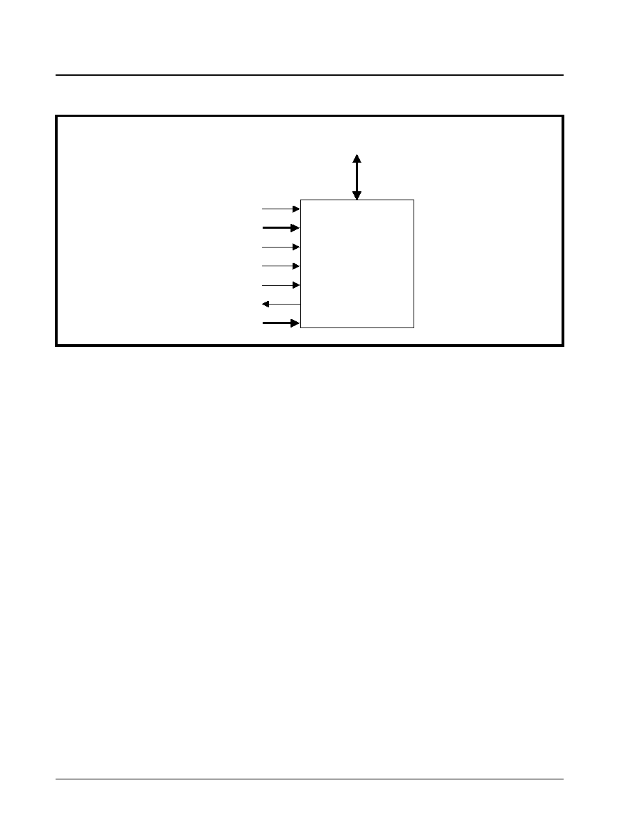
XRT7245
DS3 UNI FOR ATM
·Á
·Á
·Á
·Á
PRELIMINARY
REV. 1.03
144
6.1.2
Functional Description of the Transmit
UTOPIA Interface
The purposes of the Transmit UTOPIA interface block
are to:
∑
Receive ATM cell data from the AAL or ATM Layer
processor.
∑
Make these cells available to the Transmit Cell
Processor block.
∑
Provide some form of flow control of cell data from
the ATM Layer processor (via the TxClav output pin).
∑
Check the parity of the data received from the ATM
Layer processor, with an option to discard errored
cells.
∑ Detect and discard "Runt" cells, and resume normal
operation afterwards.
The Transmit UTOPIA Interface block consists of the
following sub-blocks.
∑
Transmit UTOPIA Input Interface
∑
Transmit UTOPIA Configuration/Status Registers
∑
Transmit UTOPIA FIFO Manager
∑ Transmit UTOPIA Cell FIFO (Tx FIFO)
The Transmit UTOPIA Interface block consists of an
input interface which complies to the "UTOPIA Level
2 interface specifications", and the Tx FIFO. The width
of the Transmit UTOPIA data bus is user-configurable to
8 or 16 bits. The incoming data bytes or words (16 bits)
are checked for odd-parity. The computed parity bit is
then compared with that presented at the TxPrty input
pin, while the corresponding data byte [word] is
present at the TxData[15:0] input. Interrupts are gen-
erated upon error conditions. Cells with parity error
may be dropped if enabled through a register setting.
The Transmit UTOPIA Interface block can be config-
ured to process 52, 53, or 54 bytes per cell. If the
ransmit UTOPIA Interface block detects a "runt" cell
(e.g., a cell that is smaller than what the Transmit
UTOPIA Interface block has been configured to
handle), it will generate an interrupt to the local µP,
discard this "Runt" cell, and resume normal operation.
The physical depth of the TxFIFO is sixteen cells with
the operating FIFO depth user-configurable to four,
eight, twelve or sixteen cells by register settings. The
incoming data (from the ATM Layer processor) is
written into the Tx FIFO where it can be read-in and
further processed by the Transmit Cell Processor. A
FIFO manager maintains the Tx FIFO and indicates
FIFO empty, FIFO full, cell space available, etc. Fig-
ure 32 presents a functional block diagram of the
Transmit UTOPIA Interface Block.
F
IGURE
31. S
IMPLE
B
LOCK
D
IAGRAM
OF
T
RANSMIT
UTOPIA I
NTERFACE
To Transmit Cell Processor
TxClk
TxData[15:0]
TxPrty
TxSoC
TxEnB
TFullB/TxClav
TxAddr[4:0]
Transmit Utopia
Interface
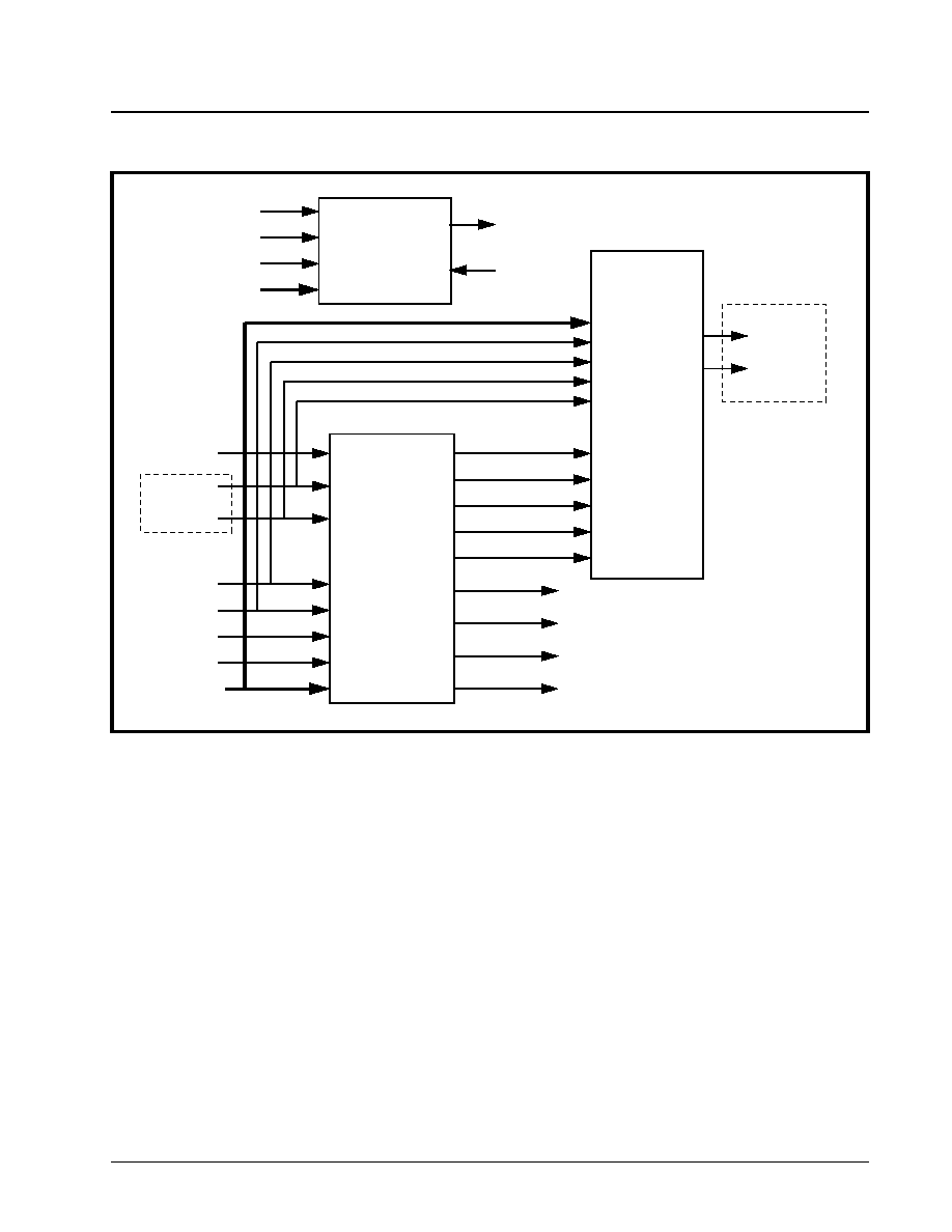
·Á
·Á
·Á
·Á
DS3 UNI FOR ATM
XRT7245
PRELIMINARY
REV. 1.03
145
The following sections discuss each functional
sub-block of the Transmit UTOPIA Interface Block in
detail. These sections will discuss the many features
associated with the Transmit UTOPIA Interface block
as well as how the user can select/configure these
features in order to suit his/her application needs.
Detailed discussion of Single-PHY and Multi-PHY
operation will each be presented in its own section
even though it involves the use of all of these
functional blocks.
6.1.2.1
Transmit UTOPIA Bus Input Interface
The Transmit UTOPIA input interface complies with
UTOPIA Level 2 standard interface (e.g., the Transmit
UTOPIA can support both Single-PHY and Multi-PHY
operations.) Additionally, the UNI provides the user
with the option of varying the following features asso-
ciated with the Transmit UTOPIA Bus Interface.
∑
Transmit UTOPIA Data Bus width of 8 or 16 bits
∑
The cell size (e.g., the number of octets being
processed per cell via the UTOPIA bus)
∑
The handling of errored cells received from the
ATM Layer processor
A discussion of the operation of the Transmit UTOPIA
Bus Interface along with each of these options will be
presented below.
6.1.2.1.1
The Pins of the Transmit UTOPIA Bus
Interface
The ATM Layer processor will interface to the Transmit
UTOPIA Interface block via the following pins.
∑
TxData[15:0]--Transmit UTOPIA Data Bus Input
pins
∑
TxAddr[4:0]--Transmit UTOPIA Address Bus Input
pins
∑
TxClk--Transmit UTOPIA Interface block clock
input pin
∑
TxSoC--Transmit "Start of Cell" indicator input pin
∑
TxPrty--Transmit UTOPIA--Odd Parity Input pin
F
IGURE
32. F
UNCTIONAL
B
LOCK
D
IAGRAM
OF
THE
T
RANSMIT
UTOPIA B
LOCK
Tx Utopia
FIFO Manager
Tx Utopia
Cell FIFO
TxData[15:0]
TxData[7:0]
TxAddr[4:0]
TxEnB
TxSoC
TxClk
TxUtopia Interrupt
Status Bits to Registers
TxClav/TxFullB
TxCel Present
TxFDat[7:0]
TuSOC
Controls from
Registers
TxFRdClk
TRdEnB
(To Tx Cell Processor)
(To Pin)
(To Interrupt block)
To Tx Cell Processor
From Tx Cell
Processor
TxUtopia
Registers
D[15:0]
A[8:0]
Status Signals
Control Signals
uP Interface

XRT7245
DS3 UNI FOR ATM
·Á
·Á
·Á
·Á
PRELIMINARY
REV. 1.03
146
∑
TxEnB*--Transmit UTOPIA Data Bus--Write
Enable input pin
∑
TxClav/TFullB*--TxFIFO Cell Available
Each of these signals are briefly discussed below.
TxData[15:0] --Transmit UTOPIA Data Bus inputs
The ATM Layer Processor will write its ATM Cell Data
into the Transmit UTOPIA Interface block, by placing
it, in a byte-wide (or word-wide) manner on these in-
put pins. The Transmit UTOPIA Data Bus can be con-
figured to operate in the "8-bit wide" or "16-bit wide"
mode (See Section 6.1.2.1.2). If the "8-bit wide"
mode is selected, then only the TxData[7:0] input
pins are active and capable of receiving data. If the
"16-bit wide" mode is selected, the all 16 input pins
(e.g., TxData[15:0]) are active. The Transmit UTOPIA
Data bus is tri-stated while the active-low TxEnB*
(Transmit UTOPIA Data Bus--Write Enable) input
signal is "high". Therefore, the ATM Layer processor
must assert this signal (e.g., toggling TxEnB* "low") in
order write the cell data, on the Transmit UTOPIA Data
bus, into the Transmit UTOPIA Interface Block. The
data on the Transmit UTOPIA Data Bus is sampled
and latched into the Transmit UTOPIA Interface
block, on the rising edge of the Transmit UTOPIA In-
terface Block Clock signal, TxClk.
Additionally, the Transmit UTOPIA Interface block will
only process one cell worth of data (e.g., 52, 53 or 54
bytes, as configured via the CellOf52Bytes option--
See Section 6.1.2.1.3), following the latest assertion
of the TxSoC (Transmit-Start of Cell) pin. Afterwards,
the Transmit UTOPIA Data bus will become tri-stated
and will cease to process any more data from the
ATM Layer Processor until the next assertion of the
TxSoC pin. Once the Transmit UTOPIA Interface
block reaches this condition, it will ignore the asser-
tions of the TxEnB* pin, and will keep the Transmit
UTOPIA Data bus input pins tri-stated until the ATM
Layer Processor pulses the TxSoC input pin, once
again.
If the Transmit UTOPIA Interface block detects a
"runt" cell (e.g., if the amount of data that is read into
the TxFIFO is less than that configured via the
"CellOf52Bytes" option), then the Transmit UTOPIA
Interface block will discard this cell, and resume nor-
mal operation.
TxAddr[4:0]--Transmit UTOPIA Address Bus
inputs
These input pins are used only when the UNI is oper-
ating in the Multi-PHY mode. Therefore, for more
information on the Transmit UTOPIA Address Bus,
please see Section 6.1.2.3.2.
TxClk--Transmit UTOPIA Interface Block Clock
signal input pin
The Transmit UTOPIA Interface block uses this signal
to sample and latch the data on the Transmit UTOPIA
Data bus into the Transmit UTOPIA Address block
(for Multi-PHY operation) into the Transmit UTOPIA
Interface block. This clock signal can run at frequencies
of 25 MHz, 33 MHz, or 50 MHz.
TxEnB*--Transmit UTOPIA Data Bus--Write
Enable input
The Transmit UTOPIA Data Bus is tri-stated while
this input signal is negated. Therefore, the ATM Layer
Processor must assert this "active-low" signal (toggle
it "low") in order to write the byte (or word) on the
Transmit UTOPIA Data Bus, into the Transmit
UTOPIA Interface block.
TxPrty--Transmit UTOPIA--Odd Parity Bit
Input Pin
The ATM Layer Processor is expected to compute
the odd-parity value of each byte (or word) of ATM
Cell data that it intends to place on the Transmit
UTOPIA Data bus. The ATM Layer Processor is then
expected to apply this parity value at the TxPrty pin,
while the corresponding byte (or word) is present on
the Transmit UTOPIA Data Bus.
TxSoC--Transmit UTOPIA--"Start of Cell"
Indicator
The ATM Layer processor is expected to pulse this
signal "high", for one clock period of TxClk, when the
first byte (or word) of a new cell is present on the
Transmit UTOPIA Data Bus. This signal must be kept
"low" at all other times.
Note: Once the ATM Layer Processor has pulsed the TxSoC
pin "high", the Transmit UTOPIA Interface Block will proceed
to read in and process only one cell of data (e.g., 52, 53, or
54 bytes, as configured via the "CellOf52Bytes" option--
See Section 6.1.2.1.3) via the Transmit UTOPIA Data Bus.
Afterwards, the Transmit UTOPIA Interface block will cease
to process any more data from the ATM Layer Processor
until the TxSoC pin has been pulsed "high" once again.
This phenomenon is more clearly defined in "Example-1"
below.
Further, if the ATM Layer Processor pulses the TxSoC
pin before the appropriate number of bytes (as con-
figured via the "CellOf52Bytes" option--See Section
6.1.2.1.3), have been read in and processed by the
Transmit UTOPIA Interface block, then a "runt" cell
·Á
·Á
·Á
·Á
DS3 UNI FOR ATM
XRT7245
PRELIMINARY
REV. 1.03
147
will have been detected. Whenever the Transmit
UTOPIA Interface block detects a "runt" cell, it will
generate a "Change in Cell Alignment" interrupt and
will discard the "runt" cell. This phenomenon is more
clearly defined in "Example-2" below.
Example-1
For example, if the user configures the Transmit
UTOPIA Interface block to process 53 bytes per cell;
then following the assertion of the TxSoC pin (which
is coincident with the placement of the first byte of the
cell on the Transmit UTOPIA Data bus), the Transmit
UTOPIA Interface block will read in and process 52
more bytes of data via the Transmit UTOPIA data bus
resulting in a total of 53 bytes being processed. After
the Transmit UTOPIA Interface block has read in the
53rd byte, it will no longer read in any more data from
the ATM Layer Processor, until the TxSoC pin has
been asserted.
Example-2
If the ATM Layer processor were to prematurely as-
serts the TxSoC pin, (e.g., when the 52nd byte is
present on the Transmit UTOPIA data bus, then the
Transmit UTOPIA Interface block will interpret the
previous 52 bytes of cell data as a "runt" cell. The
Transmit UTOPIA Interface block will then generate a
"Change of Cell Alignment" interrupt and will proceed
to discard this runt cell.
TxClav/TFullB*--Tx FIFO Cell Available/TxFIFO
Full*
This output signal is used to provide some data flow
control between the ATM Layer processor and the
Transmit UTOPIA Interface block. Please See Section
6.1.2.2.1 for more information regarding this signal.
Selecting the UTOPIA Data Bus Width
The UTOPIA data bus width can be selected to be ei-
ther 8 or 16 bits by writing the appropriate data to the
UTOPIA Configuration Register, as shown below.
If the user chooses a UTOPIA Data Bus width of 8
bits, then only the Transmit UTOPIA Data inputs:
TxData[7:0] will be active. (The input pins: TxData[15:8]
will not be active). If the user chooses a UTOPIA
Data bus width of 16 bits, then all of the Transmit
UTOPIA Data inputs: TxData[15:0] will be active. The
following table relates the value of Bit 0 (UtWidth)
within the UTOPIA Configuration Register, to the
corresponding width of the UTOPIA Data bus.
Note:
1. The selection of this bit also affects the width of the
Receive UTOPIA Data bus.
2. Upon power up or reset, the UTOPIA Data Bus
width will be 8 bits. Therefore, the user must write a
"1" to this bit in order to set the width of the Transmit
UTOPIA (and the Receive UTOPIA) to 16 bits.
6.1.2.1.2
Selecting the Cell Size (Number
of Octets per Cell)
The UNI allows the user to select the number of octets
per cell that the Transmit UTOPIA Interface block will
process, following each assertion of the TxSoC input
pin. Specifically, the user has the following cell size
options.
∑
If the UTOPIA Data Bus width is set to 8 bits then
the user can choose:
≠ 52 bytes (with no HEC byte in the cell), or
≠ 53 bytes (with either a dummy or actual HEC
byte in the cell)
∑
If the UTOPIA Data Bus width is set to 16 bits then
the user can choose:
UTOPIA Configuration Register: Address = 6Ah
B
IT
7
B
IT
6
B
IT
5
B
IT
4
B
IT
3
B
IT
2
B
IT
1
B
IT
0
Unused
Handshake Mode
M-PHY
CellOf52 Bytes
TFIFODepth[1, 0]
UtWidth16
RO
R/W
R/W
R/W
R/W
R/W
T
ABLE
11: T
HE
R
ELATIONSHIP
BETWEEN
THE
CONTENTS
OF
B
IT
F
IELD
0 (U
T
W
IDTH
16)
WITHIN
THE
UTOPIA
C
ONFIGURATION
R
EGISTER
AND
THE
OPERATING
WIDTH
OF
THE
UTOPIA D
ATA
BUS
V
ALUE
FOR
U
T
W
IDTH
16
W
IDTH
OF
UTOPIA D
ATA
B
US
0
8 bit wide Data Bus
1
16 bit wide Data Bus
XRT7245
DS3 UNI FOR ATM
·Á
·Á
·Á
·Á
PRELIMINARY
REV. 1.03
148
≠ 52 bytes (with no HEC byte in the cell), or
≠ 54 bytes (with either a dummy or actual HEC
byte, and a stuff byte in the cell)
The user makes his/her selection by writing the
appropriate data to bit 3 (CellOf52 Bytes) within the
UTOPIA Configuration Register, as depicted below.
The following table specifies the relationship between
the value of this bit and the number of octets/cell that
the Transmit UTOPIA Interface block will process.
Note: This selection applies to both the Transmit UTOPIA
and Receive UTOPIA interface blocks. Additionally, the
shaded selection reflects the default condition upon power
up or reset.
6.1.2.1.3
Parity Checking and Handling of ATM
Cell Data received from the ATM
Layer Processor
The ATM Layer processor is expected to compute the
odd parity bit for all bytes or words that it intends to
write into the Transmit UTOPIA Interface block. The
ATM Layer processor is then expected to apply the
value of this parity bit to the TxPrty input pin of the
UNI, while the corresponding byte (or word) is
present on the Transmit UTOPIA data bus. The
Transmit UTOPIA Interface block will independently
compute the odd parity of the contents on the Transmit
UTOPIA Data Bus. Afterwards, the Transmit UTOPIA
Interface block will compare its calculated value for
parity with that placed on the TxPrty input pin (by the
ATM Layer processor). If these two values are equal,
then the byte (or word) of data will be processed
through the Transmit UTOPIA Interface block. How-
ever, if these two parity values are not equal, then the
"Detection of Parity Error (Transmit UTOPIA Interface)"
interrupt will occur, and the cell comprising this er-
rored byte (or word) will be (optionally) discarded.
The user can configure the Transmit UTOPIA Inter-
face block to discard or retain this "errored" cell by
writing the appropriate data to the Transmit UTOPIA
Interrupt/Status Register (Address = 6Eh) as depict-
ed below.
If the user sets this bit to a "1", then the Transmit
UTOPIA Input Interface block will discard the errored
cell. If the user sets this bit-field to "0", then the
Transmit UTOPIA Interface block will not discard the
errored cell; and this cell will be written into the Tx FIFO.
6.1.2.2
Transmit UTOPIA FIFO Manager
The Tx FIFO Manager has the following responsibilities.
∑
Monitoring the fill level of the Tx FIFO, and provid-
ing the appropriate level of Flow Control of data
UTOPIA Configuration Register: Address = 6Ah
B
IT
7
B
IT
6
B
IT
5
B
IT
4
B
IT
3
B
IT
2
B
IT
1
B
IT
0
Unused
Handshake Mode
M-PHY
CellOf52 Bytes
TFIFODepth[1, 0]
UtWidth16
RO
R/W
R/W
R/W
R/W
R/W
T
ABLE
12: T
HE
R
ELATIONSHIP
BETWEEN
THE
CONTENTS
OF
B
IT
3 (C
ELL
O
F
52B
YTES
)
WITHIN
THE
UTOPIA
C
ONFIGURATION
R
EGISTER
,
AND
THE
NUMBER
OF
OCTETS
PER
CELL
THAT
WILL
BE
PROCESSED
BY THE
T
RANSMIT
AND
R
ECEIVE
UTOPIA I
NTERFACE
BLOCKS
.
C
ELL
O
F
52 B
YTES
N
UMBER
OF
B
YTES
/C
ELLS
0
53 bytes when the UTOPIA Data Bus width is 8 bits.
54 bytes when the UTOPIA Data Bus width is 16 bits.
1
52 bytes, regardless of the configured width of the UTOPIA Data Bus
Transmit UTOPIA Interrupt/Status Register (Address = 6Eh)
B
IT
7
B
IT
6
B
IT
5
B
IT
4
B
IT
3
B
IT
2
B
IT
1
B
IT
0
TFIFO Reset
Discard
Upon PErr
TPerr IntEn
TFIFO
ErrIntEn
TCOCA
IntEn
TPErr IntStat
TFIFO"
OverInt Stat
TCOCA
IntStat
R/W
R/W
R/W
R/W
R/W
RUR
RUR
RUR

·Á
·Á
·Á
·Á
DS3 UNI FOR ATM
XRT7245
PRELIMINARY
REV. 1.03
149
between the Transmit UTOPIA Interface block and
the ATM Layer processor.
∑
Detecting and discarding "Runt" cells and insuring
that the Tx FIFO can resume normal operation
following the removal of the runt cell.
∑ Insuring that the Tx FIFO can respond properly to
an "Overrun" condition, by generating the "Tx FIFO
Overrun Condition" interrupt, discarding the result-
ing "runt" or errored cell, and resuming proper
operation afterwards.
Transmit UTOPIA FIFO Manager Features
and Options
This section discusses the numerous features that
are provided by the Transmit UTOPIA FIFO Manager.
Additionally, this section discusses how the user can
customize these features to suit his/her application
needs.
The Transmit UTOPIA FIFO Manager provides the
user with the following options.
∑
Handshaking Mode (Octet Level vs Cell Level)
∑
User selected Operating Tx FIFO Depth
∑
Resetting the Tx FIFO
∑ Monitoring the Tx FIFO
6.1.2.3
Selecting the Handshaking Mode
(Octet Level vs Cell Level)
The Transmit UTOPIA Interface block offers two
different data flow control modes for data transmission
between the ATM Layer processor and the UNI IC.
These two modes are: "Octet-Level" Handshaking
and "Cell-Level" Handshaking; as specified by the
UTOPIA Level 2, Version 8 Specifications, and are
discussed below.
6.1.2.3.0.1
Octet-Level Handshaking
The UNI will be operating in the "Cell-Level" Hand-
shaking Mode following power up or reset. Therefore,
the user has to set bit 5 (Handshaking Mode) of the
UTOPIA Configuration Register to "0" in order to
configure the UNI into the "Octet-Level" Handshake
mode. The main signal that is responsible for data
flow control, between the ATM Layer processor and
the Transmit UTOPIA Interface block is the TxClav
output pin. The ATM Layer processor is expected to
monitor the TxClav output pin in order to determine if
it is OK to write data into the Tx FIFO. The TxClav
output pin exhibits a role that is similar to CTS (Clear
to Send) in RS-232 based data transmission systems.
As long as TxClav is at a logic "high", the ATM Layer
processor is permitted to write more cell data bytes
(or words) into the Transmit UTOPIA Interface block
(and in turn, the TxFIFO). However, when the TxClav
pin toggles "low", this indicates that the Tx FIFO can
only accept 4 (or less) more write operations from the
ATM Layer processor. Once the TxClav pin returns
high, this indicates that the TxFIFO can accept more
than 4 write operations from the ATM Layer processor,
and that the ATM Layer processor can resume writing
data to the Transmit UTOPIA Interface block.
In other words, if the UTOPIA Data bus is configured
to be 8-bits wide, then the TxClav signal will toggle
"low" when the TxFIFO can only accept 4 (or less)
bytes of ATM cell data, from the ATM Layer processor.
If the UTOPIA Data bus is configured to be 16-bits
wide; then the TxClav signal will toggle "low" when
the TxFIFO can only accept 8 (or less) bytes of ATM
cell data from the ATM Layer processor.
Figure 33 presents a timing diagram illustrating the
behavior of TxClav during writes to the Transmit
UTOPIA Interface block, while operating in the
Octet-Level Handshaking Mode.
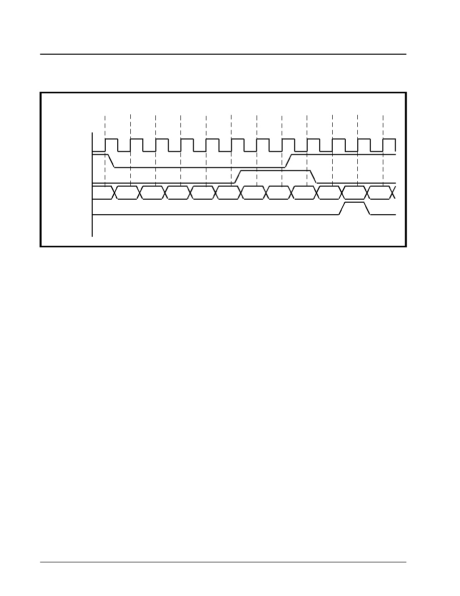
XRT7245
DS3 UNI FOR ATM
·Á
·Á
·Á
·Á
PRELIMINARY
REV. 1.03
150
Note: regarding Figure 33
1.
The Transmit UTOPIA Data Bus is configured to
be 16 bits wide. Hence, the data which the ATM
Layer processor places on the Transmit UTOPIA
Data Bus is expressed in terms of 16-bit words:
(e.g., W0≠W26).
2.
The Transmit UTOPIA Interface block is config-
ured to handle 54 bytes/cell. Hence, Figure 33
illustrates the ATM Layer processor writing 27
words (W0 through W26) for each ATM cell.
In Figure 33, TxClav is initially "high" during clock
edge # 1. However, shortly after the ATM Layer pro-
cessor writes in word W20, TxClav toggles "low",
indicating that the TxFIFO is starting to fill up. The
ATM Layer processor will detect this "negation of
TxClav" during clock edge #2; while it is writing word
W21 into the Transmit UTOPIA Interface block. At this
point, the ATM Layer processor is only permitted to
execute four more "write" operations with the Trans-
mit UTOPIA Interface block. Therefore, the ATM
Layer processor will proceed to write in words: W22,
W23, W24 and W25 before negating TxEnB*. The
ATM Layer processor must keep TxEnB* negated
until it detects that TxClav has once again returned
"high". In Figure 33, TxClav is asserted after clock
edge #8. The ATM Layer processor detects this tran-
sition in TxClav at clock edge #9; and subsequently,
asserts TxEnB*. The ATM Layer resumes writing in
more ATM cell data into the Transmit UTOPIA
Interface block.
6.1.2.3.0.2
Cell-Level Handshaking
The UNI will be operating in the "Cell-Level" Hand-
shaking mode following power up or reset. In the
"Cell-Level" Handshaking mode, when the TxClav is
at a logic "1", it means that the Tx FIFO has enough
remaining empty space for it to receive at least one
more full cell of data from the ATM Layer processor.
However, when TxClav toggles from "high" to "low", it
indicates that the very next cell (following the one that
is currently being written) cannot be accepted by the
Tx FIFO. Conversely, once TxClav has returned to
the logic "1" level, it indicates that at least one more
full cell may be written into the Tx FIFO by the ATM
Layer processor. As in the "Octet-Level" Handshake
mode, the ATM Layer processor is expected to poll
the TxClav output towards the end of transmission of
the cell currently being written and to proceed with
transmission of the next cell only if TxClav is at a log-
ic "high".
The UNI can operate in either the "Octet-Level" or the
"Cell-Level" Handshake mode, when operating in the
Single-PHY mode. However, only the "Cell-Level"
Handshake Mode is available when the UNI is oper-
ating in the Multi-PHY mode. For more information on
Single PHY and Multi PHY operation, please see
Section 6.1.2.3.
The user can configure the UNI to operate in one of
these two handshake modes by writing the appropriate
data to Bit 5 (Handshake Mode) within the UTOPIA
Configuration Register, as depicted below.
F
IGURE
33. T
IMING
D
IAGRAM
OF
T
X
C
LAV
/T
X
F
ULL
B
AND
VARIOUS
OTHER
SIGNALS
DURING
WRITES
TO
THE
T
RANSMIT
UTOPIA,
WHILE
OPERATING
IN
THE
O
CTET
-L
EVEL
H
ANDSHAKING
M
ODE
.
TxClk
TxClav
TxEnB*
TxData[15:0]
TxSoC
X
X
X
W26
W0
W1
W25
W24
W23
W22
W21
W20
1
2
3
4
5
6
7
8
9
10
11
12
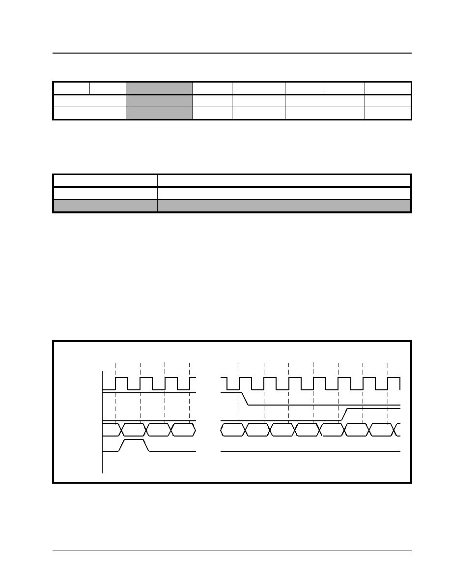
·Á
·Á
·Á
·Á
DS3 UNI FOR ATM
XRT7245
PRELIMINARY
REV. 1.03
151
The following table specifies the relationship between
this bit and the corresponding Handshaking Mode.
Note:
1. The Handshaking Mode selection applies to both the
Transmit UTOPIA Interface and Receive UTOPIA
Interface blocks.
2. Since Multi-PHY mode operation requires the use
of "Cell-Level" Handshaking, this bit-field is ignored
if the UNI is operating in the Multi-PHY mode.
3. Finally, the UNI will be operating in the "Cell-Level"
Handshaking Mode upon power up or reset.
Therefore, the user must write a "0" to this bit-field
in order to configure the UNI into the "Octet Level
Handshaking" mode.
Figure 34 presents a timing diagram that illustrates
the behavior of various Transmit UTOPIA Interface
block signals, when the Transmit UTOPIA Interface
block is operating in the "Cell-Level" Handshaking
Mode.
Note: regarding Figure 34
1. The Transmit UTOPIA Data Bus is configured to be
16 bits wide. Hence, the data which the ATM Layer
processor places on the Transmit UTOPIA Data
Bus is expressed in terms of 16-bit words: W0≠W26.
2. The Transmit UTOPIA Interface Block is configured
to handle 54 bytes/cell. Hence, Figure 34 illustrates
the ATM Layer processor writing 27 words (W0
through W26) for each ATM cell.
UTOPIA Configuration Register: Address = 6Ah
B
IT
7
B
IT
6
B
IT
5
B
IT
4
B
IT
3
B
IT
2
B
IT
1
B
IT
0
Unused
Handshake Mode
M-PHY
CellOf52 Bytes
TFIFODepth[1, 0]
UtWidth16
RO
R/W
R/W
R/W
R/W
R/W
T
ABLE
13: T
HE
R
ELATIONSHIP
BETWEEN
THE
CONTENTS
IN
BIT
FIELD
5 (H
ANDSHAKE
M
ODE
)
WITHIN
THE
UTOPIA
C
ONFIGURATION
R
EGISTER
AND
THE
R
ESULTING
UTOPIA I
NTERFACE
H
ANDSHAKE
M
ODE
.
V
ALUE
UTOPIA I
NTERFACE
H
ANDSHAKE
M
ODE
0
The UTOPIA Interfaces operate in the octet level handshake mode.
1
The UTOPIA Interfaces operate in the cell level handshake mode.
F
IGURE
34. T
IMING
D
IAGRAM
OF
VARIOUS
T
RANSMIT
UTOPIA I
NTERFACE
BLOCK
SIGNALS
,
WHEN
THE
T
RANSMIT
UTOPIA I
NTERFACE
BLOCK
IS
OPERATING
IN
THE
"C
ELL
L
EVEL
H
ANDSHAKING
" M
ODE
.
TxClk
TxClav
TxEnB*
TxData[15:0]
TxSoC
W26
W0
W1
W2
W23
W24
W25
W26
W22
X
X
1
2
3
4
24
25
26
27
28
29
30
XRT7245
DS3 UNI FOR ATM
·Á
·Á
·Á
·Á
PRELIMINARY
REV. 1.03
152
In Figure 34, the ATM Layer processor starts to write
in a new ATM cell, into the Transmit UTOPIA Interface
block, during clock edge #2. However, shortly after
the ATM Layer processor has written in word W22,
TxClav toggles "low". In the "Cell-Level" Handshaking
mode, this means that the ATM Layer processor is
not permitted to write in the subsequent cell (e.g., the
cell which is to follow the one that is currently being
written into the Transmit UTOPIA Interface block).
Hence, the ATM Layer processor must complete writ-
ing in the current cell, and then halt with any further
write operations to the Transmit UTOPIA Interface
block. Therefore, the ATM Layer processor proceeds
to write in Words W23 through W26 and then
negates the TxEnB* signal after clock edge #28. At
this point, the ATM Layer processor must wait until
TxClav toggle "high" once again; before writing in the
next ATM cell.
6.1.2.3.1
Selecting the Operating Depth of the
Tx FIFO
The physical depth of the Tx FIFO is 16 cells. However,
for various reasons the user may wish to operate with
a smaller FIFO depth. Therefore, the UNI allows the
user to select an operating depth of 4, 8, 12 or the full
16 cells. The user can make this selection by writing
the appropriate data to Bits 1 and 2 (TFIFODepth[1, 0])
within the UTOPIA Configuration Register, as depict-
ed below .
The following table presents the values for both Bits 1
and 2 (within the UTOPIA Configuration Register)
and the corresponding operating depth of the
TxFIFO.
The operating depth of the Transmit FIFO will be 16
cells upon power up or reset. Therefore, the user
must write the appropriate data to these two bit-fields
in order to change this parameter.
6.1.2.3.2
Resetting the Tx FIFO via Software
Command
The UNI allows the user to reset the Tx FIFO, via
software command, without the need to implement a
master reset of the entire UNI device. This can be
accomplished by writing the appropriate data to bit 7
(TxFIFO Reset) of the Transmit UTOPIA Interrupt
Enable/Status Register as depicted below.
UTOPIA Configuration Register: Address = 6Ah
B
IT
7
B
IT
6
B
IT
5
B
IT
4
B
IT
3
B
IT
2
B
IT
1
B
IT
0
Unused
Handshake Mode
M-PHY
CellOf52 Bytes
TFIFODepth[1, 0]
UtWidth16
RO
R/W
R/W
R/W
R/W
R/W
T
ABLE
14: T
HE
R
ELATIONSHIP
BETWEEN
T
X
FIFOD
EPTH
[1:0]
WITHIN
THE
UTOPIA C
ONFIGURATION
R
EGISTER
AND
THE
O
PERATING
D
EPTH
OF
THE
T
X
FIFO
B
IT
2
B
IT
1
O
PERATING
D
EPTH
OF
THE
T
RANSMIT
FIFO
0
0
16 cells
0
1
12 cells
1
0
8 cells
1
1
4 cells
Transmit UTOPIA--Interrupt/Status Register (Address--6Eh)
B
IT
7
B
IT
6
B
IT
5
B
IT
4
B
IT
3
B
IT
2
B
IT
1
B
IT
0
TFIFO Reset
Discard
Upon PErr
TPerr IntEn
TFIFO
ErrIntEn
TCOCA
IntEn
TPErr IntStat
TFIFO
OverInt Stat
TCOCA
IntStat
R/W
R/W
R/W
R/W
R/W
RUR
RUR
RUR
·Á
·Á
·Á
·Á
DS3 UNI FOR ATM
XRT7245
PRELIMINARY
REV. 1.03
153
6.1.2.3.3
Monitoring the Tx FIFO Status
The local
µ
P has the ability to poll and monitor the
status of the Tx FIFO via the Transmit UTOPIA FIFO
Status Register (Address = 71h). The bit format of
this register is presented below.
The following tables define the values for Bits 1 and 0
and the corresponding meaning.
6.1.2.4
UTOPIA Modes of Operation (Single
PHY and Multi-PHY operation)
The UNI chip can support both Single-PHY and
Multi-PHY operation. Each of these operating modes
are discussed below.
6.1.2.4.1
Single PHY Operation
The UNI chip will be operating in the Multi-PHY mode
upon power up or reset. Therefore, the user must write
a "1" to Bit 4 within the UTOPIA Configuration register
(Address = 6Ah) in order to configure the UNI into the
Single-PHY Mode.
Writing a `1' to this bit-field configures the UNI to op-
erate in the Single-PHY Mode. Writing a `0' config-
ures the UNI to operate in the Multi-PHY Mode.
In Single-PHY operation, the ATM layer processor is
pumping data into and receiving data from only one
UNI device, as depicted in Figure 35.
Transmit UTOPIA FIFO Status Register (Address = 71h)
B
IT
7
B
IT
6
B
IT
5
B
IT
4
B
IT
3
B
IT
2
B
IT
1
B
IT
0
Unused
TxFIFO Full
TxFIFO Empty
RO
RO
RO
RO
RO
RO
RO
RO
TxFIFO Full
T
X
FIFO F
ULL
(B
IT
1)
M
EANING
0
Tx FIFO is full, the ATM Layer processor risks causing an overrun if it writes to the TxFIFO now.
1
Tx FIFO is not full.
Tx FIFO Empty
T
X
FIFO E
MPTY
(B
IT
0)
M
EANING
0
Tx FIFO is not empty
1
Tx FIFO is empty. The Tx Cell Processor is currently generating IDLE cells
UTOPIA Configuration Register: Address = 6Ah
B
IT
7
B
IT
6
B
IT
5
B
IT
4
B
IT
3
B
IT
2
B
IT
1
B
IT
0
Unused
Handshake Mode
S-PHY/M-PHY*
CellOf52 Bytes
TFIFODepth[1, 0]
UtWidth16
RO
R/W
R/W
R/W
R/W
R/W
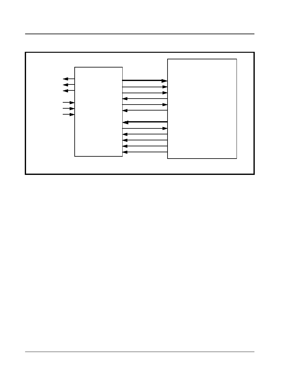
XRT7245
DS3 UNI FOR ATM
·Á
·Á
·Á
·Á
PRELIMINARY
REV. 1.03
154
This section presents a detailed description of the
Transmit UTOPIA Interface block operating in the
"Single-PHY" mode. A description of the Receive
UTOPIA Interface block operating in the "Single-PHY"
mode is presented in Section 7.4.2.2.2.1. Whenever
the ATM Layer Processor wishes to write one or a se-
ries of ATM cells to the Transmit UTOPIA Interface
block, it must do the following.
1.
Check the level of the TxClav output pin.
If the TxClav pin is "high" then there is available
space in the Tx FIFO for more ATM cell data and the
ATM Layer Processor may begin writing cell data to
the Transmit UTOPIA Interface block. However, if the
TxClav pin is "low", then the Tx FIFO is too full to ac-
cept anymore data and the ATM Layer Processor
must wait until TxClav toggles "high" before writing
any cell data to the Transmit UTOPIA Interface block.
Note: The actual meaning of TxClav toggling "low"
depends upon whether the UNI is operating in the "Cell
Level" or "Octet Level" handshake modes.
2.
Apply the first byte (or word) of the new cell to the
Transmit UTOPIA Data Bus.
The ATM Layer processor must designate this byte
(or word) as the beginning of a new cell, by pulsing
the TxSoC pin "high" for one clock period of TxClk.
3.
Apply the Odd-Parity value of this first byte (or
word), currently residing on the Transmit UTOPIA
Data Bus, to the TxPrty input pin.
This should be done concurrently with pulsing the Tx-
SoC input pin "high".
4.
Assert the "Transmit UTOPIA Data Bus"--Write
Enable Signal, TxEnb*.
This step should also be done concurrently with pulsing
the TxSoC input pin "high".
When writing the subsequent bytes (word) of the cell,
the ATM Layer Processor must repeatedly exercise
Steps 3 and 4, of the above list.
If the UNI is operating in the Octet-Level handshake
mode, then the ATM Layer processor should check
the level of the TxClav signal, at least once for every
four (4) writes of ATM cell data to the Transmit UTOPIA
Interface block.
If the UNI is operating in the Cell-Level Handshake
mode, then the ATM Layer Processor should check
the level of the TxClav signal, as it nears completion
of writing in a given cell.
The above-mentioned procedure is also depicted in
Flow-Chart Form in Figure 36; and in Timing Diagram
form in Figure 37 and 38.
F
IGURE
35. S
IMPLE
I
LLUSTRATION
OF
S
INGLE
-PHY O
PERATION
DS3 UNI
ATM Switch
(ATM Layer Device)
TxData[15:0]
RxData[15:0]
TxClav
TxPOS
TxNEG
RxPOS
RxNEG
Tx Flow Control Input
To/From
DS3 LIU
RxClav
TxSoC
TxEnB*
TxPrty
TxClk
RxClk
RxSoC
RxEnB*
RxPrty
Rx Flow Control Input
Rx Start of Cell Input
Tx Start of Cell Output
TxLineClk
RxLineClk
Rx Read Output Enable Signal
Tx Write Enable Output
Rx Utopia Data Bus Parity
Tx Utopia Data Bus Parity
Rx FIFO Clock Signal
Tx FIFO Clock Signal
Rx ATM Cell Data
Tx ATM Cell Data
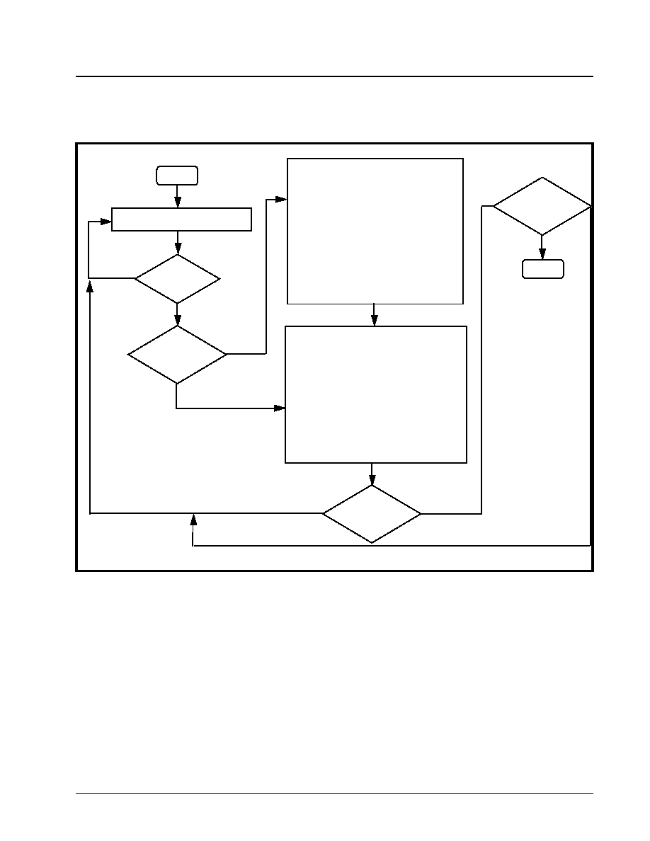
·Á
·Á
·Á
·Á
DS3 UNI FOR ATM
XRT7245
PRELIMINARY
REV. 1.03
155
F
IGURE
36. F
LOW
C
HART
DEPICTING
THE
APPROACH
THAT
THE
ATM L
AYER
P
ROCESSOR
SHOULD
TAKE
WHEN
WRITING
ATM C
ELL
D
ATA
INTO
THE
T
RANSMIT
UTOPIA I
NTERFACE
BLOCK
,
WHEN
THE
UNI
IS
OPERATING
IN
THE
S
INGLE
PHY M
ODE
.
START
Check the level of the TxClav pin.
Is
TxClav
"High"?
Is this
the first byte
(word) of a new
cell?
Is the
current Cell
Complete?
Is there
any more Cells
to write
?
END
Assert the TxSoC input pin
Place the first byte (word) on the
Transmit Utopia Data Bus.
Place the odd-parity value of this byte
(word) on the TxPrty input pin
Assert the "Transmit Utopia Data Bus
Write Enable" pin, TxEnb*.
Perform the following, concurrently
WRITING THE FIRST BYTE/WORD OF
A CELL
Perform the following, concurrently
Place the first byte (word) on the
Transmit Utopia Data Bus.
Place the odd-parity value of this byte
(word) on the TxPrty input pin
Assert the "Transmit Utopia Data Bus
Write Enable" pin, TxEnb*.
WRITING THE REMAINING BYTES/
WORDS OF A CELL
No
Yes
Yes
No
No
No
Yes
Yes

XRT7245
DS3 UNI FOR ATM
·Á
·Á
·Á
·Á
PRELIMINARY
REV. 1.03
156
Note: regarding Figure 37
1. The Transmit UTOPIA Data Bus is configured to be
16 bits wide. Hence, the data, which the ATM Layer
processor places on the Transmit UTOPIA Data
Bus, is expressed in terms of 16-bit words: W0≠W26.
2. The Transmit UTOPIA Interface Block is configured
to handle 54 bytes/cell. Hence, Figure 37 illustrates
the ATM Layer processor writing 27 words (W0
through W26) for each ATM cell.
3. The Transmit UTOPIA Interface Block is configured
to operate in the Cell-Level Handshaking mode.
Note: regarding Figure 38
1. The Transmit UTOPIA Data Bus is configured to be
16 bits wide. Hence, the data, which the ATM Layer
processor places on the Transmit UTOPIA Data
Bus, is expressed in terms of 16-bit words: W0≠W26.
2. The Transmit UTOPIA Interface Block is configured
to handle 54 bytes/cell. Hence, Figure 38 illustrates
the ATM Layer processor writing 27 words (W0
through W26) for each ATM cell.
3. The Transmit UTOPIA Interface Block is configured
to operate in the Octet-Level Handshaking Mode.
F
IGURE
37. T
IMING
D
IAGRAM
OF
ATM L
AYER
PROCESSOR
T
RANSMITTING
D
ATA
TO
THE
UNI
OVER
THE
UTOPIA
D
ATA
B
US
, (S
INGLE
-PHY M
ODE
/C
ELL
-L
EVEL
H
ANDSHAKING
).
TxClk
TxClav
TxEnB*
TxData[15:0]
TxSoC
W26
W0
W1
W2
W23
W24
W25
W26
W22
X
X
1
2
3
4
24
25
26
27
28
29
30
F
IGURE
38. T
IMING
D
IAGRAM
OF
ATM L
AYER
P
ROCESSOR
T
RANSMITTING
D
ATA
TO
THE
UNI
OVER
THE
UTOPIA
D
ATA
B
US
(S
INGLE
-PHY M
ODE
/O
CTET
-L
EVEL
H
ANDSHAKING
).
TxClk
TxClav
TxEnB*
TxData[15:0]
TxSoC
X
X
X
W26
W0
W1
W25
W24
W23
W22
W21
W20
1
2
3
4
5
6
7
8
9
10
11
12
·Á
·Á
·Á
·Á
DS3 UNI FOR ATM
XRT7245
PRELIMINARY
REV. 1.03
157
Final Comments on Single-PHY Operation
The important thing to note about the Single-PHY
mode is that the TxClav pin is used as a data flow
control pin, and has a role somewhat similar to RTS
(Request To Send) in RS-232 based data transmis-
sion. The TxClav pin will have a slightly different role
when the UNI is operating in the Multi-PHY mode.
The UNI, while operating in Single PHY mode, can be
configured for either "Octet-Level" or "Cell Level"
Handshaking. In either case, the ATM Layer processor
is expected to poll the TxClav output pin before writing
the next byte, word or cell to the TxFIFO.
6.1.2.4.2
Multi PHY Operation
The UNI IC will be operating in the "Multi-PHY" mode
upon power up or reset. In the "Multi-PHY" operating
mode, the ATM Layer processor may be writing data
into and reading data from several UNI devices in
parallel. When the UNI is operating in the Multi-PHY
mode, the Transmit UTOPIA Interface block will sup-
port two kinds of operations with the ATM Layer pro-
cessor:
∑
Polling for "available" UNI devices.
∑ Selecting which UNI (out of several possible UNI
devices) to write ATM cell data to.
Each of these operations are discussed in the sections
below. However, prior to discussing each of these
operations, the reader must understand the following.
"Multi-PHY" operation involves the use of one (1) ATM
Layer processor and several UNI devices, within a
system. The ATM Layer processor is expected to
read/write ATM cell data from/to these UNI devices.
Hence, "Multi-PHY" operation requires, at a minimum,
some means for the ATM Layer processor to uniquely
identify a UNI device (within the "Multi-PHY" system)
that it wishes to "poll", write ATM cell data to, or read
ATM cell data from. Actually, "Multi-PHY" operation
provides an addressing scheme which allows the
ATM Layer processor to uniquely identify "UTOPIA
Interface Blocks" (e.g., Transmit and Receive) within
all of the UNI devices operating in the "Multi-PHY"
system. In order to uniquely identify a given "UTOPIA
Interface block", within a "Multi-PHY" system, each
"UTOPIA Interface Block is assigned a 5-bit "UTOPIA
address" value. The user assigns this address value
to a particular "Transmit UTOPIA Interface block" by
writing this address value into the "Tx UTOPIA
Address Register" (Address = 70h) within its "host"
UNI device. The bit-format of the "Tx UTOPIA
Address Register" is presented below.
Likewise, the user assigns a "UTOPIA address" value
to a particular "Receive UTOPIA Interface block",
within one of the UNIs (in the "Multi-PHY" system) by
writing this address value into the "Rx UTOPIA Address
Register" (Address = 6Ch) within the "host" UNI device.
The bit-format of the "Rx UTOPIA Address Register"
is presented below.
Note: The role of the Receive UTOPIA Interface block, in
"Multi-PHY" operation is presented in Section 7.4.2.2.2.2.
6.1.2.4.2.1
ATM Layer Processor "polling" of
the UNIs, in the Multi-PHY Mode
When the UNI is operating in the "Multi-PHY" mode,
the Transmit UTOPIA Interface block will automatically
be configured to support "polling". "Polling" allows an
ATM Layer processor (which is interfaced to several
UNI devices) to determine which UNIs are capable of
receiving and handling additional ATM cell data, at
any given time. The manner in which the ATM Layer
processor "polls" its UNI devices, follows.
Tx UTOPIA Address Register (Address = 70h)
B
IT
7
B
IT
6
B
IT
5
B
IT
4
B
IT
3
B
IT
2
B
IT
1
B
IT
0
Unused
Tx_UTOPIA_Addr[4:0]
RO
RO
RO
R/W
R/W
R/W
R/W
R/W
0
0
0
0
0
0
0
0
Rx UTOPIA Address Register (Address = 6Ch)
B
IT
7
B
IT
6
B
IT
5
B
IT
4
B
IT
3
B
IT
2
B
IT
1
B
IT
0
Unused
Rx_UTOPIA_Addr[4:0]
RO
RO
RO
R/W
R/W
R/W
R/W
R/W
0
0
0
0
0
0
0
0
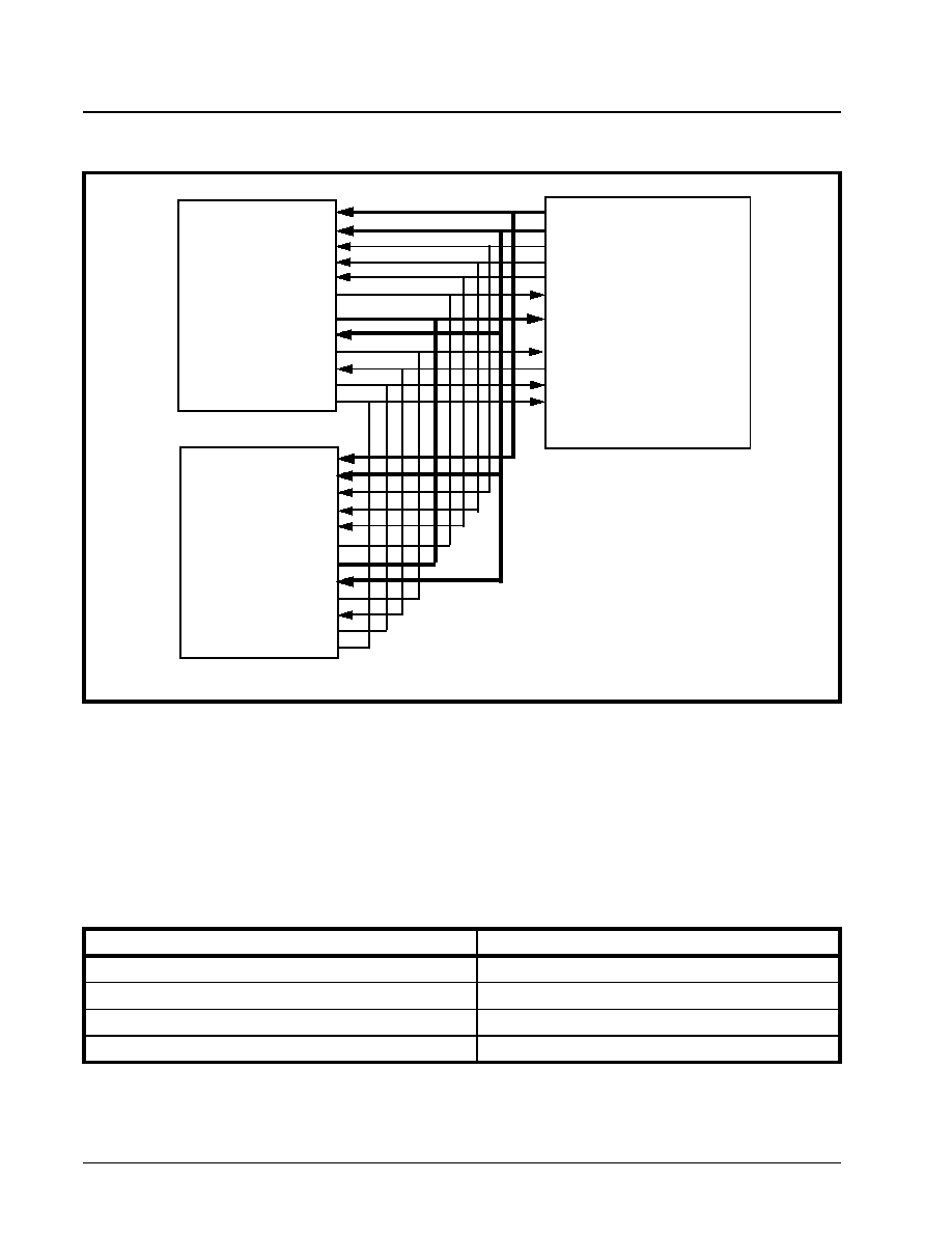
XRT7245
DS3 UNI FOR ATM
·Á
·Á
·Á
·Á
PRELIMINARY
REV. 1.03
158
Figure 39 depicts a "Multi-PHY" system consisting of
an ATM Layer processor and two (2) UNI devices,
which are designated as "UNI #1" and "UNI #2". In
this figure, both of the UNIs are connected to the ATM
Layer processor via a common "Transmit UTOPIA" Da-
ta Bus, a common "Receive UTOPIA" Data Bus, a
common "TxClav" line, a common "RxClav" line, as
well as common TxEnB*, RxEnB*, TxSoC and RxSoC
lines. The ATM Layer processor will also be addressing
both the Transmit and Receive UTOPIA Interface
blocks via a common "UTOPIA" address bus
(Ut_Addr[4:0]) Therefore, the Transmit and Receive
UTOPIA Interface Blocks, within a given UNI might
have different addresses; as depicted in Figure 39.
The UTOPIA Address values that have been assigned
to each of the Transmit and Receive UTOPIA Interface
blocks, within Figure 39, are listed below in Table 15.
Recall that the Transmit UTOPIA Interface blocks were
assigned these addresses by writing these values into
the "Tx UTOPIA Address Register" (Address = 70h)
within their "host" UNI device. The discussion of the
Receive UTOPIA Interface blocks, within UNIs #1
and #2 is presented in Section 7.4.2.2.2.2.1.
F
IGURE
39. A
N
I
LLUSTRATION
OF
M
ULTI
-PHY O
PERATION
WITH
UNI D
EVICES
#1
AND
#2
TxData[15:0]
TxAddr[4:0]
TxPrty
TxEnb*
TxSoC
TxClav
RxData[15:0]
RxAddr[4:0]
RxPrty
RxEnb*
RxSoC
RxClav
UNI # 1
TxAddr = 00h
RxAddr = 01h
TxData[15:0]
TxAddr[4:0]
TxPrty
TxEnb*
TxSoC
TxClav
RxData[15:0]
RxAddr[4:0]
RxPrty
RxEnb*
RxSoC
RxClav
TxAddr = 02h
RxAddr = 03h
TxData[15:0]
Ut_Addr[4:0]
Tx_Parity
Tx_Ut_WR*
Tx_SoC_out
TxClav_In
RxData[15:0]
Rx_Parity
Rx_Ut_Rd*
Rx_SoC_In
RxClav_In
ATM Layer Processor
UNI # 2
T
ABLE
15: UTOPIA A
DDRESS
V
ALUES
OF
THE
UTOPIA I
NTERFACE
BLOCKS
ILLUSTRATED
IN
F
IGURE
39.
B
LOCK
UTOPIA A
DDRESS
V
ALUE
Transmit UTOPIA Interface block--UNI #1
00h
Receive UTOPIA Interface block--UNI #1
01h
Transmit UTOPIA Interface block--UNI #2
02h
Receive UTOPIA Interface block--UNI #2
03h

·Á
·Á
·Á
·Á
DS3 UNI FOR ATM
XRT7245
PRELIMINARY
REV. 1.03
159
Polling Operation
Consider that the ATM Layer processor is currently
writing a continuous stream of ATM cell data into UNI
#1. While writing this cell data into UNI #1, the ATM
Layer processor can also "poll" UNI #2 for "availability"
(e.g., tries to determine if the ATM Layer processor
can write any more ATM cell data into the "Transmit
UTOPIA Interface block" within UNI #2).
The ATM Layer Processor's Role in the "Polling"
Operation
The ATM Layer processor accomplishes this "polling"
operation by executing the following steps.
1.
Assert the TxEnB* input pin (if it is not asserted
already).
The UNI device (being "polled") will know that this is
only a "polling" operation, if the TxEnB* input pin is
asserted, prior to detecting its UTOPIA Address on
the "UTOPIA Address" bus.
2.
The ATM Layer processor places the address of
the Transmit UTOPIA Interface Block of UNI #2
onto the UTOPIA Address Bus, Ut_Addr[4:0],
3.
The ATM Layer processor will then check the
value of its "TxClav_in" input pin (see Figure 37).
The UNI Devices Role in the "Polling" Operation
UNI #2 will sample the signal levels placed on its Tx
UTOPIA Address input pins (TxAddr[4:0]) on the rising
edge of its "Transmit UTOPIA Interface block" clock
input signal, TxClk. Afterwards, UNI #2 will compare
the value of these "Transmit UTOPIA Address Bus
input pin" signals with that of the contents of its "Tx
UTOPIA Address Register (Address = 70h).
If these values do not match, (e.g., TxAddr[4:0] ¶02h)
then UNI #2 will keep its "TxClav" output signal "tri-
stated"; and will continue to sample its "Transmit
UTOPIA Address bus input" pins; with each rising
edge of TxClk.
If these two values do match, (e.g., TxAddr[4:0] = 02h)
then UNI #2 will drive its "TxClav" output pin to the
appropriate level, reflecting its TxFIFO "fill-status".
Since the UNI is automatically operating in the "Cell
Level Handshaking" mode while it is operating in the
"Multi-PHY" mode; the UNI will drive the TxClav out-
put signal "high" if it is capable of receiving at least
one more complete cell of data from the ATM Layer
processor. Conversely, the UNI will drive the "TxClav"
output signal "low" if its TxFIFO is too full and is inca-
pable of receiving one more complete cell of data
from the ATM Layer processor.
When UNI #2 has been selected for "polling", UNI #1
will continue to keeps its "TxClav" output signal "tri-
stated". Therefore, when UNI #2 is driving its "TxClav"
output pin to the appropriate level, it will be driving
the entire "TxClav" line, within the "Multi-PHY" system.
Consequently, UNI#2 will also be driving the
"TxClav_in" input pin of the ATM Layer processor
(see Figure 39).
If UNI #2 drives the "TxClav" line "low", upon the appli-
cation of its address on the UTOPIA Address Bus,
then the ATM Layer processor will "learn" that it cannot
write any more cell data to this UNI device; and will
deem this device "unavailable". However, if UNI #2
drives the TxClav line "high" (during "polling"), then the
ATM Layer processor will know that it can write cell data
into the Transmit UTOPIA Interface block, of UNI # 2.
Figure 40 presents a timing diagram that depicts the
behavior of the ATM Layer processor's and the UNI's
signals during polling.
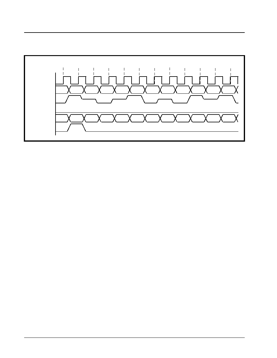
XRT7245
DS3 UNI FOR ATM
·Á
·Á
·Á
·Á
PRELIMINARY
REV. 1.03
160
Note: regarding Figure 40
1. The Transmit UTOPIA Data Bus is configured to be
16 bits wide. Hence, the data, which the ATM Layer
processor places on the Transmit UTOPIA Data
bus, is expressed in terms of 16-bit words: (e.g.,
W0≠W26.)
2. The Transmit UTOPIA Interface Block is configured
to handle 54 bytes/cell. Hence, Figure 40 illustrates
the ATM Layer processor writing 27 words (W0
through W26) for each ATM cell.
3. The ATM Layer processor is currently writing ATM
cell data to the Transmit UTOPIA Interface Block,
within UNI #1 (TxAddr[4:0] = 00h) during this "poll-
ing process".
4. The TxFIFO, within UNI#2's Transmit UTOPIA
Interface block (TxAddr[4:0] = 02h) is incapable of
receiving any additional ATM cell data from the
ATM Layer processor. Hence, the TxClav line will
be driven "low" whenever this particular Transmit
UTOPIA Interface block is "polled".
5. The Transmit UTOPIA Address of 1Fh is not asso-
ciated with any UNI device, within this "Multi-PHY"
system. Hence, the TxClav line is tri-stated when-
ever this address is "polled".
Note: Although Figure 39 depicts connections between
the Receive UTOPIA Interface block pins and the ATM
Layer processor; the Receive UTOPIA Interface block oper-
ation, in the Multi-PHY mode, will not be discussed in this
section. Please see Section 7.4.2.2.2.2 for a discussion on
the Receive UTOPIA Interface block during Multi-PHY
operation.
6.1.2.4.2.2
Writing ATM Cell Data
into a Different UNI
After the ATM Layer processor has "polled" each of
the UNI devices within its system, it must now select
a UNI, and begin writing ATM cell data to that device.
The ATM Layer processor makes its selection and
begins the writing process by:
1.
Applying the UTOPIA Address of the "target" UNI
on the "UTOPIA Address Bus".
2.
Negate the TxEnB* signal. This step causes the
"addressed" UNI to recognize that it has been
selected to receive the next set of ATM cell data
from the ATM Layer processor.
3.
Assert the TxEnB* signal.
4.
Assert the TxSoC input pin.
5.
Begin applying the ATM Cell data in a byte-wide
(or word-wide) manner to the Transmit UTOPIA
Data Bus.
Figure 41 presents a flow-chart that depicts the "UNI
Device Selection and Write" process in Multi-PHY
operation.
F
IGURE
40. T
IMING
D
IAGRAM
ILLUSTRATING
THE
B
EHAVIOR
OF
VARIOUS
SIGNALS
FROM
THE
ATM L
AYER
PROCESSOR
AND
THE
UNI,
DURING
P
OLLING
.
TxClk
TxAddr[4:0]
TxClav
TxEnB*
TxData[15:0]
TxSoC
00h
1Fh
02h
1Fh
00h
02h
1Fh
02h
00h
1Fh
00h
02h
W27
W0
W1
W2
W3
W4
W5
W6
W7
W8
W9
W10
00h
02h
00h
02h
02h
00h
00h
1
2
3
4
5
6
7
8
9
10
11
12
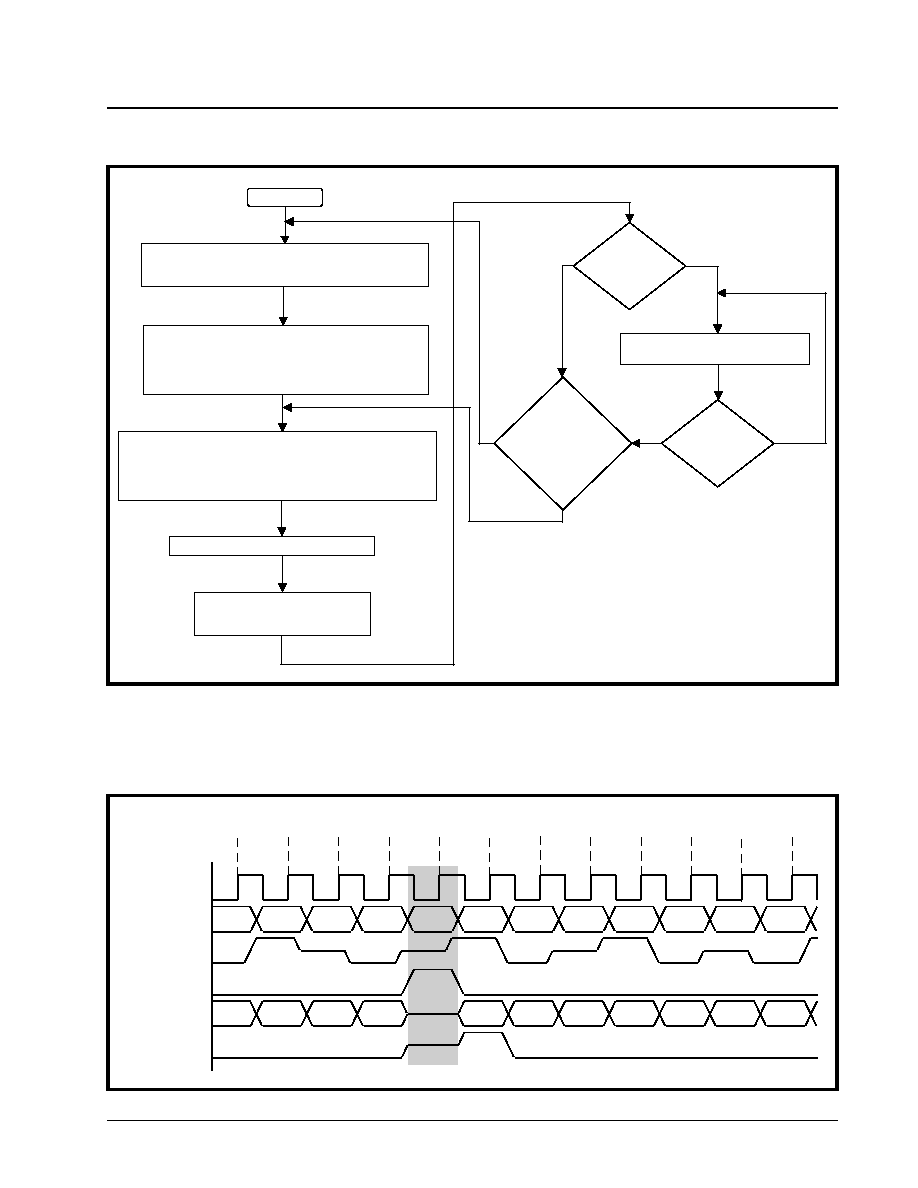
·Á
·Á
·Á
·Á
DS3 UNI FOR ATM
XRT7245
PRELIMINARY
REV. 1.03
161
Figure 42 presents a timing diagram that illustrates
the behavior of various "Transmit UTOPIA Interface
block" signals during the "Multi-PHY" UNI Device
Selection and Write operation.
F
IGURE
41. F
LOW
-C
HART
OF
THE
"UNI D
EVICE
S
ELECTION
AND
W
RITE
P
ROCEDURE
"
FOR
THE
M
ULTI
-PHY O
PERATION
.
START
Poll all UNIs within the "Multi-PHY" System
Determine which UNIs are "Available"
Select "Available" UNI
1. Apply Utopia Address of the Transmit Utopia
Interface block onto the "Utopia Address" bus
2. Negate the TxEnB* signal
Begin writing ATM cell data into "Selected" UNI
1. Assert TxEnB*
2. Place first byte/word of ATM cell onto the "Transmit
Utopia Data Bus & Assert TxSoC
Continue to write ATM Cell data
Check the TxClav level after
writing 48 bytes of cell data
Is
TxClav
"High"
?
Wait for TxClav to toggle "high"
Is
TxClav
"High"
?
Is
there any more
ATM cell data to be
written to selected
UNI?
Yes
No
Yes
Yes
No
No
F
IGURE
42. T
IMING
D
IAGRAM
OF
THE
T
RANSMIT
UTOPIA D
ATA
AND
A
DDRESS
B
US
SIGNALS
,
DURING
THE
"M
ULTI
-PHY" UNI D
EVICE
S
ELECTION
AND
W
RITE
O
PERATIONS
.
TxClk
TxAddr[4:0]
TxClav
TxEnB*
TxData[15:0]
TxSoC
00h
1Fh
02h
1Fh
00h
02h
1Fh
00h
02h
1Fh
02h
00h
W0
W1
W2
W3
W4
W5
W6
W26
W25
W24
W23
Cell Transmitted to 02h
Cell Transmitted to 00h
00h
02h
00h
02h
00h
02h
02h
1
2
3
4
5
6
7
8
9
10
11
12
XRT7245
DS3 UNI FOR ATM
·Á
·Á
·Á
·Á
PRELIMINARY
REV. 1.03
162
Note: regarding Figure 42
1. The Transmit UTOPIA Data bus is configured to be
16 bits wide. Hence, the data which the ATM Layer
processor places on the Transmit UTOPIA Data
bus, is expressed in terms of 16-bit words (e.g.,
W0≠W26).
2. The Transmit UTOPIA Interface Block is configured
to handle 54 bytes/cell. Hence, Figure 42 illus-
trates the ATM Layer processor writing 27 words
(e.g., W0 through W26) for each ATM cell.
In Figure 42, the ATM Layer processor is initially writ-
ing ATM cell data to the Transmit UTOPIA Interface
block within UNI #2 (TxAddr[4:0] = 02h). However,
the ATM Layer processor is also polling the Transmit
UTOPIA Interface block within UNI #1 (TxAddr[4:0] =
00h) and some "non-existent" device at TxAddr[4:0] =
1Fh. The ATM Layer processor completes its writing
of the cell to UNI #1 at clock edge #4. Afterwards, the
ATM Layer processor will cease to write any more
cell data to UNI #1, and will begin to write this data
into UNI #2 (TxAddr[4:0] = 02h). The ATM Layer pro-
cessor will indicate its intentions to select a new UNI
device for writing by negating the TxEnB* signal, at
clock edge #5 (see the shaded portion of Figure 42).
At this time, UNI #1 will notice two things:
1.
The UTOPIA Address for the Transmit UTOPIA
Interface block, within UNI #1 is on the Transmit
UTOPIA Address bus (TxAddr[4:0] = 00h).
2.
The TxEnB* signal has been negated.
UNI #1 will interpret this signaling as an indication
that the ATM Layer processor is going to be perform-
ing write operations to it. Afterwards, the ATM Layer
processor will begin to write ATM cell data into Trans-
mit UTOPIA Interface block, within UNI #1.
6.1.2.5
Transmit UTOPIA Interrupt Servicing
The Transmit UTOPIA Interface block will generate
interrupts upon the following conditions:
∑
Detection of parity errors
∑
Change of cell alignment (e.g., the detection of
"runt" cells)
∑ TxFIFO Overrun
If one of these conditions occur and if that particular
condition is enabled for interrupt generation, then
when the local µP/µC reads the UNI Interrupt status
register, as shown below; it should read "xxxx1xxxb"
(where the b suffix denotes a binary expression, and
the "x" denotes a "don't care" value).
At this point, the local µC/µP has determined that the
Transmit UTOPIA Interface block is the source of the
interrupt, and that the Interrupt Service Routine
should branch accordingly.
The next step in the interrupt service routine should
be to determine which of the three Transmit UTOPIA
Interface Block interrupt conditions has occurred and
is causing the Interrupt request. In order to accomplish
this, the local µP/µC should now read the Tx UT In-
terrupt Enable/Status Register, which is located at
address 6Eh within the UNI device. The bit format of
this register is presented below.
UNI Interrupt Status Register (Address = 05h)
B
IT
7
B
IT
6
B
IT
5
B
IT
4
B
IT
3
B
IT
2
B
IT
1
B
IT
0
Rx DS3
Interrupt
Status
Rx PLCP
Interrupt
Status
Rx CP
Interrupt
Status
Rx UTOPIA
Interrupt
Status
Tx UTOPIA
Interrupt
Status
Tx CP
Interrupt
Status
Tx DS3
Interrupt
Status
One Sec
Interrupt
Status
RO
RO
RO
RO
RO
RO
RO
RUR
x
x
x
x
1
x
x
x
Tx UT Interrupt Enable /Status Register (Address-6Eh)
B
IT
7
B
IT
6
B
IT
5
B
IT
4
B
IT
3
B
IT
2
B
IT
1
B
IT
0
TFIFO
Reset
Discard
Upon
PErr
TPerr
Interrupt
Enable
Tx FIFO
ErrInt
Enable
TCOCA
Interrupt
Enable
TPErr
Interrupt
Status
Tx FIFO
OverInt
Status
TCOCA
Interrupt
Status
R/W
R/W
R/W
R/W
R/W
RUR
RUR
RUR
·Á
·Á
·Á
·Á
DS3 UNI FOR ATM
XRT7245
PRELIMINARY
REV. 1.03
163
The "Tx UT Interrupt Enable/Status" Register has
eight bit-fields. However, only six of these bit fields
are relevant to interrupt processing. Bits 0≠2 are the
interrupt status bits and bits 3≠5 are the interrupt en-
able bits for the Transmit UTOPIA Interface block.
Each of these "interrupt processing relevant" bit fields
are defined below.
Bit 0--TCOCA Interrupt Status--Transmit UTOPIA
Change of Cell Alignment Condition
If the ATM Layer Processor asserts the TxSoC input
pin prior to writing the contents of a complete cell (as
configured via the CellOf52Bytes option) on the
Transmit UTOPIA Data Bus, then the Transmit UTOPIA
Interface block will interpret this newly received cell
data as a "runt" cell. When the Transmit UTOPIA In-
terface block detects a "runt" cell, it will generate the
"Transmit UTOPIA Change of Cell Alignment Condi-
tion" interrupt, and the "runt" cell will be discarded.
The Transmit UTOPIA Interface Block will indicate
that it is generating this kind of interrupt by asserting
Bit 0 (TCOCA Interrupt Status) within the Transmit
UTOPIA Interrupt Enable/Status Register, as depict-
ed below.
Bit 1--Tx FIFO Overrun Interrupt Status
If the Tx FIFO is filled to capacity, and if the ATM Layer
processor attempts to write any additional data to the
Tx FIFO, some of the data within the Tx FIFO will be
overwritten, and in turn lost. If the Transmit UTOPIA
Interface block detects this condition, and if this
interrupt condition has been enabled then the UNI will
assert the INT* pin to the local µP/µC. Additionally, the
UNI will set bit-field 1, (TxFIFO Overrun Interrupt
Status) within the Tx UTOPIA Interrupt Enable/Status
Register to "1", as depicted below.
Bit 1 of the Tx UT Interrupt Enable/Status register will
be reset or cleared upon the local µP/µC reading this
register. This action will also negate bit 3 within the
UNI Interrupt Status Register and the INTB* output
pin, unless other outstanding interrupt conditions are
awaiting service.
Bit 2--TPErr Interrupt Status--Detection of Parity
Error via the Transmit UTOPIA Interface Block
The ATM Layer processor is expected to compute and
present the odd-parity value of each byte or word of
ATM Cell data that it intends place on the Transmit
UTOPIA Data bus. As the ATM Layer processor is
writing ATM cell data into the Transmit UTOPIA Inter-
face block, it will place the value of this parity bit at
the TxPrty input pin of the UNI device while the
corresponding byte (or word) is present on the Transmit
UTOPIA data bus. The Transmit UTOPIA Interface
block will read the contents of the Transmit UTOPIA
Data Bus, and will independently compute the odd-
parity value of that byte or word. Afterwards, the
Transmit UTOPIA Interface block will then compare
its computed parity value with that presented at the
TxPrty input (by the ATM Layer processor). If these
Tx UT Interrupt Enable /Status Register (Address-6Eh)
B
IT
7
B
IT
6
B
IT
5
B
IT
4
B
IT
3
B
IT
2
B
IT
1
B
IT
0
TFIFO
Reset
Discard
Upon
Parity Error
Tx UT Parity
Error
Interrupt
Enable
Tx FIFO
Overrun
Interrupt
Enable
TCOCA
Interrupt
Enable
Tx UT Parity
Error
Interrupt
Status
Tx FIFO
Overrun
Interrupt
Status
TCOCA
Interrupt
Status
R/W
R/W
R/W
R/W
R/W
RUR
RUR
RUR
x
x
x
x
1
x
x
1
Transmit UTOPIA Interrupt Enable /Status Register (Address--6Eh)
B
IT
7
B
IT
6
B
IT
5
B
IT
4
B
IT
3
B
IT
2
B
IT
1
B
IT
0
TFIFO
Reset
Discard
Upon
Parity
Error
Tx UT Parity
Error
Interrupt
Enable
Tx FIFO
Overrun
Interrupt
Enable
TCOCA
Interrupt
Enable
Tx UT Parity
Error
Interrupt
Status
Tx FIFO
Overrun
Interrupt
Status
TCOCA
Interrupt
Status
R/W
R/W
R/W
R/W
R/W
RUR
RUR
RUR
x
x
x
1
x
x
1
x
XRT7245
DS3 UNI FOR ATM
·Á
·Á
·Á
·Á
PRELIMINARY
REV. 1.03
164
two parity values are different then a "Transmit UTOPIA
Parity error" has been detected. If this interrupt condi-
tion has been enabled, then the UNI will generate the
"Detection of Parity Error" interrupt. Additionally, the
UNI will set bit-field 2 (Tx UT Parity Error Interrupt
Status), within the Transmit UTOPIA Interrupt Enable/
Status Register to "1", as depicted below.
Once the local µP/µC has read the contents of the
Tx UT Interrupt Enable/Status register, then bit 3 of
the UNI Interrupt Status Register, Bit 2 of the Tx UT
Interrupt Enable/Status register, and the INTB* output
pin will all be negated, unless outstanding interrupt
conditions are awaiting servicing.
Bit 3--TCOCA Interrupt Enable--Transmit UTOPIA
Change of Cell Alignment Interrupt Enable
This "read/write" bit-field allows the user to enable or
disable the "Change of Cell Alignment" interrupt. The
local microprocessor can enable this interrupt by writ-
ing a "1" to this bit-field. Upon power up or reset con-
ditions, this bit-field will contain a "0". Therefore the
default condition is for this interrupt to be disabled.
Bit 4--Tx FIFO ErrInt Enable--Tx FIFO Overrun
Condition Interrupt Enable
This "Read/Write" bit-field allows the user to enable
or disable the "Tx FIFO Overrun" interrupt. The local
microprocessor can enable this interrupt by writing a
"1" to this bit. Upon power up or reset conditions, this
bit will contain a "0". Therefore the default condition is
for this interrupt to be disabled. The local micropro-
cessor must write a "1" to this bit in order to enable
this interrupt.
Transmit UTOPIA Interrupt Enable /Status Register (Address-6Eh)
B
IT
7
B
IT
6
B
IT
5
B
IT
4
B
IT
3
B
IT
2
B
IT
1
B
IT
0
Tx FIFO
Reset
Discard
Upon
Parity Error
Tx UT Parity
Error
Interrupt
Enable
Tx FIFO
Overrun
Interrupt
Enable
TCOCA
Interrupt
Enable
Tx UT Parity
Error
Interrupt
Status
Tx FIFO
Overrun
Interrupt
Status
TCOCA
Interrupt
Status
R/W
R/W
R/W
R/W
R/W
RUR
RUR
RUR
x
x
1
x
x
1
x
x
Tx UT Interrupt Enable/Status Register (Address-6Eh)
B
IT
7
B
IT
6
B
IT
5
B
IT
4
B
IT
3
B
IT
2
B
IT
1
B
IT
0
Tx FIFO
Reset
Discard
Upon Parity
Error
Tx UT Parity
Error
Interrupt
Enable
Tx FIFO
Overrun
Interrupt
Enable
TCOCA
Interrupt
Enable
Tx UT Parity
Error
Interrupt
Status
Tx FIFO
Overrun
Interrupt
Status
TCOCA
Interrupt
Status
R/W
R/W
R/W
R/W
R/W
RUR
RUR
RUR
·Á
·Á
·Á
·Á
DS3 UNI FOR ATM
XRT7245
PRELIMINARY
REV. 1.03
165
Bit 5--TPerr Interrupt Enable--Detection of Parity
Error in Transmit UTOPIA Block Interrupt Enable
This "Read/Write" bit-field allows the user to enable
or disable the "Detected Parity error" interrupt. The
user can enable this interrupt by writing a "1" to this
bit. Upon power up or reset conditions, this bit will
contain a "0". Therefore the default condition is for
this interrupt to be disabled. The user must write a "1"
to this bit in order to enable this interrupt.
6.2
Transmit Cell Processor
6.2.1
Brief Description of the Transmit
Cell Processor
The Transmit Cell Processor reads in cells from the
Transmit UTOPIA FIFO (Tx FIFO) within the Transmit
UTOPIA Interface block. Immediately after reading in
the cell from the TxFIFO, the Transmit Cell Processor
will verify the "Data Path Integrity Check" pattern
(located in octet # 5, within this cell). Afterwards, the
Transmit Cell Processor optionally computes and
inserts the HEC byte into each cell and optionally
scrambles the cell payload bytes. When the TxFIFO
does not contain a full cell, the Transmit Cell Processor
generates a programmable idle (or unassigned) cell
and inserts it in the transmit stream. The Transmit Cell
Processor provides the user with the ability to write
an "outbound" OAM cell into the "Transmit OAM Cell"
buffer, and to transmit this OAM cell, upon demand.
Additionally, the Transmit Cell Processor is also
equipped with a serial input port which allows the
user to externally insert the value of the GFC (Generic
Flow Control) field for each outbound cell. Figure 43
presents a simple illustration of the Transmit Cell
Processor block and the associated external pins.
Figure 43 presents a functional block diagram of the
Transmit Cell Processor.
Tx UT Interrupt Enable /Status Register (Address-6Eh)
B
IT
7
B
IT
6
B
IT
5
B
IT
4
B
IT
3
B
IT
2
B
IT
1
B
IT
0
Tx FIFO
Reset
Discard
Upon Parity
Error
Tx UT Parity
Error
Interrupt
Enable
Tx FIFO
Overrun
Interrupt
Enable
TCOCA
Interrupt
Enable
Tx UT Parity
Error
Interrupt
Status
Tx FIFO
Overrun
Interrupt
Status
TCOCA
Interrupt
Status
R/W
R/W
R/W
R/W
R/W
RUR
RUR
RUR
F
IGURE
43. S
IMPLE
I
LLUSTRATION
OF
THE
T
RANSMIT
C
ELL
P
ROCESSOR
B
LOCK
AND
THE
A
SSOCIATED
E
XTERNAL
P
INS
Transmit Cell
Processor
TxCellTxed
TxGFCClk
TxGFCMSB
TxGFC
From Transmit Utopia
Interface
To Transmit PLCP
Processor
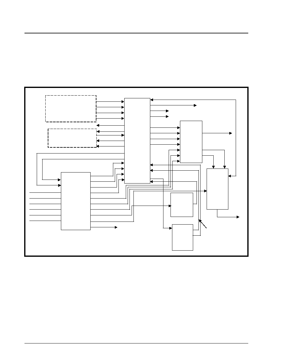
XRT7245
DS3 UNI FOR ATM
·Á
·Á
·Á
·Á
PRELIMINARY
REV. 1.03
166
6.2.2
Functional Description of Transmit
Cell Processor
The Transmit Cell Processor consists of the following
functional blocks.
∑
Configuration and Status Register
∑
Controller
∑
HEC Byte Calculator
∑
OAM Cell Processor
∑
Cell Scrambler
∑
IDLE Cell Generator
∑
"Transmit GFC Nibble-field" serial input port
Most of these functional blocks will be discussed in
some detail below. The Transmit Cell Processor will
read in ATM Cell Data from the Tx FIFO. The first four
bytes of each cell is loaded into the "HEC Byte calcu-
lator". The fifth byte of each cell will be read-in and
compared against a pre-defined "Data Path Integrity
Check" pattern. While this "check" is being performed;
the "HEC Byte Calculator" will take these first four
bytes of the cell, and compute a HEC byte value. This
HEC byte value will be written (or inserted) into the
5th octet position of the cell. Consequently, the "Data
Path Integrity Check" pattern will now be overwritten.
Bytes 6 through 53 (the cell payload) of each cell, are
sent onto the "Cell Scrambler" and are summarily
"scrambled". Afterwards, the cell is reassembled
(with the first four header bytes, the newly computed
HEC byte and scrambled payload), and is routed to
the Transmit PLCP Processor or Transmit DS3 Framer.
When a complete cell is not available in the TxFIFO, a
cell is created by the "Idle Cell Generator". The user
has the option of specifying the contents of the header
and payload of these Idle Cells via the µP-accessible
registers. The payload of the Idle Cell will be pro-
grammed with a repeating pattern of a byte contained
within an on-chip register. From this point on, the Idle
Cell is processed in the same manner as is an as-
signed (e.g., user or OAM) cell. A valid HEC byte is
F
IGURE
44. F
UNCTIONAL
B
LOCK
D
IAGRAM
OF
THE
T
RANSMIT
C
ELL
P
ROCESSOR
B
LOCK
DataBusL[7:0]
DataBusH[7:0]
ReadB
WriteB
CSB
Configuration
and Status
Registers
TUSoC
TCelPresent
TFDat
CellOf52
TxGFC
TxGFCClk
TxGFCMSB
SendOAM
TDPChkPat
ICHECCalcEn
HECInsEn
OAMSent
TDPIntegFail
Controller
CosetIn
GFCInsEn
HECErrMask
HEC
Calculator
HECEn
GFC[3:0]
HECSoC
TICCount
TCellCount
TxCelTxed
TCelRdClk
From Framer/PLCP
Scrambler
Idle Cell
Generator
OAM
Processor
TCelData[7:0]
ScramblerEn
TxCPInt
To Interrupt
Block
HECDat[7:0]
HeaderLoc
OAMCycle
OAMDataL[7:0]
OAMDataH[7:0]
ICDat[7:0]
From TxUtopia
To/From Pins
TxCPRegSel
ICGRegSel[5:0]
TFIFORdENB
TFIFORCLK
H_PL
FIFOrlCDAT[7:0]
·Á
·Á
·Á
·Á
DS3 UNI FOR ATM
XRT7245
PRELIMINARY
REV. 1.03
167
computed over the four bytes of the programmed idle
cell header and is inserted into the fifth octet position.
The user has the option to disable the HEC Byte
Calculation and Insertion features for Idle cells, and
the contents of the fifth-header byte programmed
register may be transmitted directly.
The Transmit Cell Processor allows the user to transmit
pre-programmed OAM cells upon demand. The content
of this OAM cell is stored in an on-chip RAM location,
which will be referred to as the "Transmit OAM Cell
Buffer". When the local µP decides to transmit the
OAM cell to the "Far-End" Terminal, it writes a "1" to a
certain register bit. The Transmit Cell Processor will
then proceed to read in the contents of the "Transmit
OAM Cell" buffer, and form a cell from this data. This
OAM cell will be subsequently processed like any user
or Idle cell (e.g., processed through the HEC Byte
Calculator and Cell Scrambler) and then routed to the
Transmit PLCP Processor (or Transmit DS3 Framer).
As mentioned earlier, the Transmit Cell Processor will
perform a "Data Path Integrity Check" on all user cells
that it reads from the TxFIFO. More specifically, the
Transmit Cell Processor will look for a specific data
pattern that should be residing within octet #5 of
these cells. The purpose of this test is to verify the in-
tegrity of the communication link throughout the "ATM
Layer processor" system. This "Data Path Integrity
Pattern" was written into the cell by the Receive Cell
Processor of another UNI, prior to its entry into the
"ATM Layer processor" system. If the Transmit Cell
Processor detects a discrepancy between the con-
tents of octet #5 and the expected pattern, then the
Transmit Cell Processor will generator a "Data Path
Integrity Check" error interrupt. After the Transmit
Cell Processor has completed checking for the "Data
Path Integrity Check" pattern; within a given cell, it
will (optionally) overwrite this pattern by inserting the
HEC byte.
The Transmit Cell Processor will inform external
circuitry when a cell has been transmitted from the
Transmit Cell Processor to either the Transmit PLCP
Processor or the Transmit DS3 Framer, by pulsing the
"TxCellTxed" output pin.
6.2.2.1
HEC Byte Calculation and Insertion
The "HEC Byte Calculator" takes the first four bytes
of each cell and computes a CRC-8 value via the
generating polynomial x
8
+ x
2
+ x + 1. The user has
the option to have the coset polynomial x
6
+ x
4
+ x
2
+
1 modulo-2 added to the CRC-8 byte and, instead in-
sert this newly computed value into byte 5 of the cell
before transmission. The user has the following addi-
tional options regarding the "HEC Byte Calculator".
∑
HEC Byte Calculation and Insertion Enable/Disable
for user and OAM cells.
∑
HEC Byte Calculation and Insertion Enable/Disable
for Idle Cells.
∑ Inserting errors into the HEC byte, for chip/equipment
testing purposes.
The implementation and result of selecting each of
these options are presented below.
6.2.2.1.1
Configuring the HEC Byte Calculator
for User and OAM Cells
The user can enable or disable the "HEC Byte Calcu-
lation and Insertion" feature for user and OAM cells.
The user can exercise this option by writing the ap-
propriate value to Bit 5 of the TxCP Control Register,
as depicted below.
If the user opts to disable this feature, then the HEC
byte will not be computed and the contents within the
fifth octet position of each cell (e.g., typically the "Data
Path Integrity Check" pattern) will be transmitted to the
Transmit PLCP (or Transmit DS3 Framer) block as is.
The following table relates the content of this bit-field
to the "HEC Byte Calculator's" handling of valid (e.g.,
user or OAM) cells.
TxCP Control Register (Address = 60h)
B
IT
7
B
IT
6
B
IT
5
B
IT
4
B
IT
3
B
IT
2
B
IT
1
B
IT
0
Scrambler
En
Coset
Enable
HEC Insert
Enable
TDPChk
Pattern
GFC Insert
Enable
TDPErr
Interrupt
Enable
Idle Cell
HEC CalEn
TDPErr
Interrupt
Status
R/W
R/W
R/W
R/W
R/W
R/W
R/W
RUR
1
1
x
1
0
0
1
0
XRT7245
DS3 UNI FOR ATM
·Á
·Á
·Á
·Á
PRELIMINARY
REV. 1.03
168
Upon power up or reset, the "HEC Byte Calculator
and Insertion" feature is enabled. The user must
write a "0" to this bit in order to disable this operation.
6.2.2.1.2
Configuring the "HEC Byte Calculator
and Insertion" Feature for Idle Cells
The user can separately enable or disable the "HEC
Byte Calculation and Insertion" feature for the outbound
Idle Cells. The user can exercise this option by writ-
ing the appropriate value to bit 1 (Idle Cell HEC
CalEn) within the TxCP Control Register, as depicted
below.
This "Read/Write" bit-field allows the user to enable
and disable the "Calculation and Insertion" of the
HEC byte into the Idle Cell as illustrated below. If the
user chooses to disable this feature, then the 5th oc-
tet of the Idle Cells will be transmitted to the Transmit
PLCP (or Transmit DS3 Framer) block as pro-
grammed in the "Tx CP Idle Cell Pattern Header--
Byte 5" register (Address = 68h).
Upon power up or reset, the Transmit Cell Processor
will be configured such that the HEC bytes will be
calculated and inserted into the fifth octet position of
each Idle Cell. The user must write a "0" to this bit-
field in order to disable this feature.
6.2.2.1.3
Modulo-2 Addition of Coset
Polynomial to the HEC Byte Value
When enabled, the HEC Byte Calculator takes the
first four bytes of each cell and computes a CRC-8
value via the generating polynomial x
8
+ x
2
+ x + 1.
The BISDN Physical Layer specifications (ITU
Recommendations I.432) specifies that this CRC-8 (or
HEC) value can optionally be modulo-2 added to the
polynomial x
6
+ x
4
+ x
2
+ 1; and inserting the result of
this calculation into the fifth byte of each cell. The pur-
pose of this option is to provide protection against bit
slips. This protection is not required in transmission
systems that ensure adequate one's density. Howev-
er, this operation does provide protection against all ze-
ros cells that could be passed to the ATM Layer during
a loss of signal condition on the transmission medium.
The ATM Forum UNI specifications also requires this
operation.
T
ABLE
16: T
HE
R
ELATIONSHIP
BETWEEN
THE
CONTENTS
OF
B
IT
-
FIELD
5 (HEC I
NSERT
E
NABLE
)
WITHIN
THE
T
X
CP
C
ONTROL
R
EGISTER
,
AND
THE
HEC B
YTE
C
ALCULATOR
'
S
HANDLING
OF
VALID
CELLS
HEC I
NSERT
E
NABLE
R
ESULT
0
HEC Byte Calculation is disabled and the 5th byte is transmitted to the Transmit PLCP Block
(or Transmit DS3 Framer) as is
1
The HEC Byte is calculated and is inserted into the 5th octet position of each valid cell.
TxCP Control Register (Address = 60h)
B
IT
7
B
IT
6
B
IT
5
B
IT
4
B
IT
3
B
IT
2
B
IT
1
B
IT
0
Scrambler
En
Coset
Enable
HEC Insert
Enable
TDPChk
Pattern
GFC Insert
Enable
TDPErr
Interrupt
Enable
Idle Cell
HEC
CalEn
TDPErr
Interrupt
Status
R/W
R/W
R/W
R/W
R/W
R/W
R/W
RUR
1
1
1
1
0
0
x
0
T
ABLE
17: T
HE
R
ELATIONSHIP
BETWEEN
THE
CONTENTS
WITHIN
B
IT
1 (IC HEC C
ALC
E
N
)
OF
THE
"T
X
CP C
ONTROL
R
EGISTER
"
AND
THE
RESULTING
HANDLING
OF
I
DLE
C
ELLS
,
BY
THE
"HEC B
YTE
C
ALCULATOR
"
IC HEC C
ALC
E
N
R
ESULT
0
The entire programmed Idle Cell header is transmitted without Modification
1
The HEC byte is calculated, via the first four bytes of the header, and is inserted into the fifth octet
position within each Idle Cell.
·Á
·Á
·Á
·Á
DS3 UNI FOR ATM
XRT7245
PRELIMINARY
REV. 1.03
169
The user can enable or disable this modulo-2 addi-
tion, by writing the appropriate value to bit 6 (Coset
Enable) within the "TxCP Control" Register, as de-
picted below.
A "1" in this bit-field will enable this modulo addition.
Conversely, a "0" in this bit-field will disable this
operation.
Upon power up or reset, the Transmit Cell Processor
will be configured such that the coset polynomial is
modulo-2 added to the HEC byte prior to insertion in-
to the cell. The user must write a "0" to this bit in or-
der to disable this operation.
6.2.2.1.4
Inserting Errors into the HEC Byte
via Software Control
The XRT7245 DS3 UNI allows the user to insert errors
into the HEC bytes of "outbound" cells in order to
support equipment testing. One such test that the user
may wish to verify is that the HEC byte verification
(e.g., error detection and/or correction) features of
some "Far-End" terminal equipment is functioning
properly. The user would conduct this test by trans-
mitting cells with erroneous HEC byte values to the
"unit under test" (UUT). The user can exercise this
option by writing the appropriate data into the TxCP
Error Mask register, which is located at address 62h
within the UNI.
The Transmit Cell Processor automatically XORs the
HEC Byte (or each "outbound" cell) with the contents
of this register. The result of this operation is written
back into the fifth octet position of each of these cells.
Therefore, if the user does not wish to inject errors in-
to the HEC byte, he/she should insure that the con-
tents of this register is 00h, the default value.
6.2.2.2
The Cell Scrambler
The Cell Scrambler takes bytes 6 through 53 of each
cell (the payload) and scrambles the contents of these
bytes. The purpose of scrambling the cell payload
bytes is to reduce the possibility of the contents of
the cell payload mimicking patterns that are used for
framing and cell delineation purposes. The scrambler
generating polynomial is x
43
+ 1. The user can enable
or disable the Cell Scrambler by setting or clearing bit 7
(Scrambler Enable) within the "TxCP Control" Register,
as depicted below.
TxCP Control Register (Address = 60h)
B
IT
7
B
IT
6
B
IT
5
B
IT
4
B
IT
3
B
IT
2
B
IT
1
B
IT
0
Scrambler
En
Coset
Enable
HEC Insert
Enable
TDPChk
Pattern
GFC Insert
Enable
TDPErr
Interrupt
Enable
Idle Cell
HEC CalEn
TDPErr
Interrupt
Status
R/W
R/W
R/W
R/W
R/W
R/W
R/W
RUR
TxCP Error Mask Register; (Address = 62h)
B
IT
7
B
IT
6
B
IT
5
B
IT
4
B
IT
3
B
IT
2
B
IT
1
B
IT
0
HEC Error Mask Byte
R/W
R/W
R/W
R/W
R/W
R/W
R/W
R/W
TxCP Control Register (Address = 60h)
B
IT
7
B
IT
6
B
IT
5
B
IT
4
B
IT
3
B
IT
2
B
IT
1
B
IT
0
Scrambler
Enable
Coset
Enable
HEC Insert
Enable
TDPChk
Pattern
GFC Insert
Enable
TDPErr
Interrupt
Enable
Idle Cell
HEC CalEn
TDPErr
Interrupt
Status
R/W
R/W
R/W
R/W
R/W
R/W
R/W
RUR
x
1
1
1
0
0
1
0
XRT7245
DS3 UNI FOR ATM
·Á
·Á
·Á
·Á
PRELIMINARY
REV. 1.03
170
A "1" in this bit-field enables the Cell Scrambler. Con-
versely, a "0" in this bit-field disables the Cell-Scrambler.
Upon power up or reset, the Cell Scrambler function
will be enabled. Therefore, the user must write a "0"
to this bit in order to disable cell scrambling.
6.2.2.3
GFC Nibble-Field Serial Input Port
The first four bits in the first header byte of each cell
are allocated for carrying "Generic Flow Control" (GFC)
information. The user can externally insert his/her own
values for the GFC nibble-field into each outbound
cell, via a serial input port. The user will activate this
serial input port (the "Transmit GFC-Nibble-field" Serial
Input port) by writing a "1" to bit 3 (GFC Insert Enable)
of the "TxCP Control" Register, as depicted below.
Once the user has activated the "Transmit GFC Nibble-
field" Serial input port, it will accept the 4 bit GFC val-
ue via the TxGFC pin during each cell processing pe-
riod. The TxGFC serial input port will be expecting
the bits of the GFC nibble-field in descending order
(MSB first). The GFC bits are clocked into the serial
input port via the rising edge of the clock signal,
TxG-FCClk. Since these four bits must be provided
for each cell; TxGFCClk will provide four clock edges
during each cell processing period. The "Transmit
GFC Nibble-field" Serial input port will also provide a
"framing pulse" in the form of the TxGFCMSB output
pin pulsing "high". This output pin will pulse "high"
when the Transmit Cell Processor is ready to receive
the MSB (most significant bit) of the GFC field.
Figure 45 presents a timing diagram illustrating the
role of each of these signals during GFC insertion.
6.2.2.4 OAM Cell Processing
The UNI chip provides on-chip RAM space for the
storage of the complete contents (header and pay-
load) of an OAM cell. This RAM space is known as
the "Transmit OAM Cell" buffer (consisting of 54
bytes) and is located at 136h through 16Bh in the
UNI address space. Therefore, in order to "load" the
TxCP Control Register (Address = 60h)
B
IT
7
B
IT
6
B
IT
5
B
IT
4
B
IT
3
B
IT
2
B
IT
1
B
IT
0
Scrambler
Enable
Coset
Enable
HEC Insert
Enable
TDPChk
Pattern
GFC Insert
Enable
TDPErr
Interrupt
Enable
Idle Cell
HEC CalEn
TDPErr
Interrupt
Status
R/W
R/W
R/W
R/W
R/W
R/W
R/W
RUR
1
1
1
1
x
0
1
0
F
IGURE
45. B
EHAVIOR
OF
T
X
GFC, T
X
GFCC
LK
,
AND
T
X
GFCMSB
DURING
GFC
INSERTION
INTO
THE
"O
UTBOUND
" C
ELL
TxGFCClk
TxGFCMSB
t14
TxGFC
t16
BIT 3
BIT 2
BIT 1
BIT 0
t17
t13
t15
·Á
·Á
·Á
·Á
DS3 UNI FOR ATM
XRT7245
PRELIMINARY
REV. 1.03
171
OAM cell into the "Transmit OAM Cell" buffer, the lo-
cal µP must write this data into this address location
within the UNI IC, via the Microprocessor Interface.
Afterwards, whenever the user wishes to transmit the
OAM cell, the local µP must to write a "1" to bit 7
(SendOAM) within the TxCP OAM Register as
depicted below.
If the local µP writes a "1" bit 7 (or 1xxxxxxxb) to the
TxCP OAM Register; then the Transmit Cell Proces-
sor will read-in the contents of the "Transmit OAM
Cell" buffer, and form it into a cell. This OAM cell will
then be routed to the HEC Byte Calculator and Cell
Scrambler within the Transmit Cell Processor block,
prior to transmittal to the Transmit PLCP Processor
(or Transmit DS3 Framer). Bit 7 of the TxCP OAM
Register will be reset (to "0") upon completion of the
transmission of the OAM cell. The user may also poll
this bit in order to determine whether or not the OAM
cell has been sent.
The user can monitor the number of valid cells (e.g.,
user and OAM cells) that have been generated and
transmitted to the Transmit PLCP Processor or the
Transmit DS3 Framer. The Transmit Cell Processor
increments the contents of the "PMON Transmitted
Valid Cell Count (MSB and LSB)" Registers (Address
= 3Ah, and 3Bh) for each valid cell that it generates.
These two registers are "Reset-upon-Read" registers
that when concatenated present a 16-bit representa-
tion of the total number of "valid cells" generated and
transmitted by the Transmit Cell Processor, since the
last read of these registers. The bit-format of these
two registers follows:
6.2.2.4
Idle Cell Processing
Whenever the TxFIFO (within the Transmit UTOPIA
Interface block) does not contain a complete cell, the
Transmit Cell Processor will automatically generate
and process Idle Cells. The user can customize the
contents of these Idle Cells or he/she can use the de-
fault values that are provided by the UNI chip. The
user can customize the contents of these Idle Cells
by programming six different registers:
∑
TxCP Idle Cell Pattern--Header Byte 1
∑
TxCP Idle Cell Pattern--Header Byte 2
∑
TxCP Idle Cell Pattern--Header Byte 3
∑
TxCP Idle Cell Pattern--Header Byte 4
∑
TxCP Idle Cell Pattern--Header Byte 5
∑ TxCP Transmit Cell Payload
Table 18 presents the Bit Format of each of these
Registers and Table 19 presents the Address and
Default values of these cells.
TxCP OAM Register (Address = 61h)
B
IT
7
B
IT
6
B
IT
5
B
IT
4
B
IT
3
B
IT
2
B
IT
1
B
IT
0
SendOAM
Unused
Semaphore
RO
RO
RO
RO
RO
RO
RO
PMON Transmitted Valid Cell Count--MSB (Address = 3Ah)
B
IT
7
B
IT
6
B
IT
5
B
IT
4
B
IT
3
B
IT
2
B
IT
1
B
IT
0
Tx Valid Cell Count--High Byte
RUR
RUR
RUR
RUR
RUR
RUR
RUR
RUR
0
0
0
0
0
0
0
0
PMON Transmitted Valid Cell Count--LSB (Address = 3Bh)
B
IT
7
B
IT
6
B
IT
5
B
IT
4
B
IT
3
B
IT
2
B
IT
1
B
IT
0
Tx Valid Cell Count--Low Byte
RUR
RUR
RUR
RUR
RUR
RUR
RUR
RUR
0
0
0
0
0
0
0
0

XRT7245
DS3 UNI FOR ATM
·Á
·Á
·Á
·Á
PRELIMINARY
REV. 1.03
172
The role of the registers for Idle Cell Pattern--Bytes 1
through 4 is quite straightforward. When the Transmit
Cell Processor opts to generate an Idle cell, it will
read in the content of these registers and send these
values onto the HEC Byte Calculator. Consequently,
the contents of the "Transmit Idle Cell Pattern--
Header Byte 5" will likely be overwritten by the HEC
Byte Calculator in the Idle Cell, unless the HEC Byte
Calculator has been disabled (See Section 6.2.2.1.2).
The payload portion of these Idle Cells is defined by
the contents of the Transmit Idle Cell Payload Register
(Address = 69h), repeated 48 times. When the Transmit
Cell Processor reads in this register to form the cell
payload, the resulting payload will be sent on to the
Cell Scrambler and is (optionally) scrambled just like
any assigned cell.
The UNI will keep track of the number of Idle cells
that have been generated and transmitted to the
Transmit PLCP Processor (or the Transmit DS3
Framer). The Transmit Cell Processor increments the
contents of the "PMON Transmitted Idle Cell Count
(MSB and LSB)" Registers (Address = 38h and 39h)
for each Idle Cell that is generated and transmitted.
These two registers are "Reset-upon-Read" registers
that, when concatenated, presents a 16-bit represen-
tation of the total number of idle cells generated and
transmitted since the last time these registers were
read. The bit format of these two registers follow.
T
ABLE
18: B
IT
F
ORMAT
OF
THE
T
X
CP I
DLE
C
ELL
P
ATTERN
-H
EADER
B
YTES
AND
T
X
CP C
ELL
P
AYLOAD
R
EGISTERS
R
EGISTER
B
IT
7
B
IT
6
B
IT
5
B
IT
4
B
IT
3
B
IT
2
B
IT
1
B
IT
0
TxCP Idle Cell Pattern--Header Byte 1
Transmit Idle Cell Pattern--Header Byte 1
TxCP Idle Cell Pattern--Header Byte 2
Transmit Idle Cell Pattern--Header Byte 2
TxCP Idle Cell Pattern--Header Byte 3
Transmit Idle Cell Pattern--Header Byte 3
TxCP Idle Cell Pattern--Header Byte 4
Transmit Idle Cell Pattern--Header Byte 4
TxCP Idle Cell Pattern--Header Byte 5
Transmit Idle Cell Pattern--Header Byte 5
TxCP Idle Cell Payload
Transmit Idle Cell Payload
T
ABLE
19: A
DDRESS
AND
D
EFAULT
V
ALUES
OF
THE
T
X
CP I
DLE
C
ELL
P
ATTERN
R
EGISTERS
A
DDRESS
R
EGISTER
D
EFAULT
V
ALUE
64h
TxCP Idle Cell Pattern--Header Byte 1
00h
65h
TxCP Idle Cell Pattern--Header Byte 2
00h
66h
TxCP Idle Cell Pattern--Header Byte 3
00h
67h
TxCP Idle Cell Pattern--Header Byte 4
01h
68h
TxCP Idle Cell Pattern--Header Byte 5
52h
69h
TxCP Idle Cell Payload
5Ah
PMON Transmitted Idle Cell Count--MSB (Address = 38h)
B
IT
7
B
IT
6
B
IT
5
B
IT
4
B
IT
3
B
IT
2
B
IT
1
B
IT
0
Tx Idle Cell Count--High Byte
RO
RO
RO
RO
RO
RO
RO
RO
0
0
0
0
0
0
0
0
·Á
·Á
·Á
·Á
DS3 UNI FOR ATM
XRT7245
PRELIMINARY
REV. 1.03
173
6.2.2.5
Data Path Integrity Check
The Transmit Cell Processor provides for some
performance monitoring of the communication link
between the various UNIs, over the "ATM Switching
System". This performance monitoring feature is re-
ferred to as the "Data Path Integrity Check".
The Receive Cell Processor, or some equivalent entity,
within a UNI device, will (after performing HEC byte
verification) write a "Data Path Integrity Check" pattern
into each cell prior to its being read and processed by
the ATM Layer processor. This cell (with the "Data
Path Integrity Check" pattern) will be routed through
the ATM switch, and possibly throughout the Wide
Area Network (WAN); before arriving to the Transmit
UTOPIA Interface block of a given XRT7245 DS3
UNI. The Transmit Cell Processor will read in this cell
from the Tx FIFO, and will, prior to inserting a new
HEC byte into the cell, read in the fifth octet from the
Tx FIFO and check it for a specific pattern or value.
The user can configure the Transmit Cell Processor
to check for either a constant "55h" pattern or an al-
ternating pattern of "55h" and "AAh" for each cell. The
user can also configure the Transmit Cell Processor
to generate an interrupt if a Data Path Integrity Test
fails. The user can accomplish all of this by writing
the appropriate data to the "Tx CP Control" Register
(Address = 60h). The bit format (with the relevant bit
fields shaded) of this register is shown below.
Note:
1. The "Data Path Integrity Check" feature is disabled
if the Transmit (and Receive) UTOPIA Interface
blocks have been configured to handle 52 byte cells.
2. This "Data Path Integrity Test" is only performed on
user cells. The Transmit Cell Processor does not
perform this test on OAM or Idle Cells.
The role that each of these "shaded" bit field plays is
presented below.
Bit 4--TDPChk Pat--Test Data Path Integrity
Check Pattern
The Transmit Cell Processor is always checking for a
specific pattern in the fifth octet of a user cell re-
trieved from the Tx FIFO. This "Read/Write" bit allows
the user to specify the octet pattern that the Transmit
Cell Processor should be checking for. The following
table relates the contents of this bit field to the octet
pattern expected by the Transmit Cell Processor.
PMON Transmitted Idle Cell Count--LSB (Address = 39h)
B
IT
7
B
IT
6
B
IT
5
B
IT
4
B
IT
3
B
IT
2
B
IT
1
B
IT
0
Tx Idle Cell Count--Low Byte
RO
RO
RO
RO
RO
RO
RO
RO
0
0
0
0
0
0
0
0
Tx CP Control Register (Address = 60h)
B
IT
7
B
IT
6
B
IT
5
B
IT
4
B
IT
3
B
IT
2
B
IT
1
B
IT
0
Scrambler
Enable
Coset
Enable
HEC Insert
Enable
TDPChk
Pattern
GFC Insert
Enable
TDPErr Interrupt
Enable
Idle Cell
HEC CalEn
TDPErr Interrupt
Status
R/W
R/W
R/W
R/W
R/W
R/W
R/W
RUR
T
ABLE
20: T
HE
R
ELATIONSHIP
BETWEEN
THE
CONTENTS
OF
B
IT
4 (TDPC
HK
P
AT
)
WITHIN
THE
T
X
CP C
ONTROL
R
EGISTER
,
AND
THE
"D
ATA
P
ATH
I
NTEGRITY
C
HECK
" P
ATTERN
THAT
THE
T
RANSMIT
C
ELL
P
ROCESSOR
WILL
LOOK
FOR
IN
THE
5
TH
OCTET
OF
EACH
INCOMING
USER
CELL
TDPC
HK
P
AT
"D
ATA
P
ATH
I
NTEGRITY
P
ATTERN
" E
XPECTED
BY
THE
T
RANSMIT
C
ELL
P
ROCESSOR
0
Transmit Cell Processor expects an alternating "55h/AAh" pattern for the value of the fifth octet of the
cells received from the Tx FIFO.
1
Transmit Cell Processor expects a constant "55h" pattern for the value of the fifth octet of the cells
received from the Tx FIFO.
XRT7245
DS3 UNI FOR ATM
·Á
·Á
·Á
·Á
PRELIMINARY
REV. 1.03
174
The remaining shaded bits are "Interrupt service" re-
lated and will be discussed in the following section.
6.2.2.6
Transmit Cell Processor Interrupt
Servicing
The Transmit Cell Processor generates interrupts up-
on the detection of an error in the "Data Path Integrity
Check" pattern.
If this condition occurs, and if that particular is en-
abled for interrupt generation, then the UNI will gen-
erate the "Data Path Integrity Check Pattern Error" in-
terrupt. Afterwards, when the local µP/µC reads the
UNI Interrupt Status Register, as shown below; it
should read "xxxxx1xxb" (where the b suffix denotes
a binary expression, and the "x" denotes a "don't
care" value).
At this point, the local µC/µP has determined that the
Transmit Cell Processor block is the source of the in-
terrupt, and that the Interrupt Service Routine should
branch accordingly.
Since the Transmit Cell Processor contains only one
interrupt source, the Interrupt Service Routine, in this
case should perform a read of the "Tx CP Control"
Register (Address = 60h) in order to verify and service
this condition. The bit format of this register is
presented below.
This register contain 8 active bit-fields. However, only
two of these bit-fields are relevant to Interrupt
Processing. Bit 0 is an Interrupt Status bit, and Bit 2
is an Interrupt Enable bit.
Bit 2-- TDPErrIntEn--"Test Data Path Integrity
Check" Interrupt Enable
This "Read/Write" bit-field allows the user to enable
or disable the "Data Path Integrity Check Pattern Er-
ror" interrupt. Writing a "0" to this bit-field disables
this interrupt. Likewise, writing a "1" to this bit-field
enables this interrupt.
Bit 0--TDPErrIntStat--"Test Data Path Integrity
Check" Interrupt Status
This "Reset-upon-Read" bit-field indicates whether or
not the "Data Path Integrity Check Pattern Error" in-
terrupt has occurred since the last reading of the "Tx
CP Control" Register. This interrupt will occur if the
Transmit Cell Processor detects a byte-pattern, in the
fifth octet position of each cell read from the TxFIFO,
that differs from the expected "Data Path Integrity
Check" pattern.
A "1" in this bit-field indicates that this interrupt has
occurred since the last reading of the "Tx CP Control"
Register. A "0" in this bit-field indicates that this inter-
rupt has not occurred.
Note: Once the local µP has read this register, Bit 0
(TDPerr Interrupt Status) will be reset to "0". Additionally,
Bit 3 (Tx CP Interrupt Status) within the "UNI Interrupt
Status" register will also be reset to "0".
6.3
Transmit PLCP Processor
6.3.1
Brief Description of the Transmit
PLCP Processor
The Transmit PLCP Processor takes the incoming
cells (assigned, Idle, or OAM) from the Transmit Cell
Processor and packs them into PLCP frames. Each of
these PLCP frames also includes various overhead
UNI Interrupt Status Register (Address = 05h)
B
IT
7
B
IT
6
B
IT
5
B
IT
4
B
IT
3
B
IT
2
B
IT
1
B
IT
0
Rx DS3
Interrupt
Status
Rx PLCP
Interrupt
Status
Rx CP
Interrupt
Status
Rx UTOPIA
Interrupt
Status
Tx UTOPIA
Interrupt
Status
Tx CP
Interrupt
Status
Tx DS3
Interrupt
Status
One Sec
Interrupt
Status
RO
RO
RO
RO
RO
RO
RO
RO
0
x
x
x
1
x
x
x
Transmit Cell Processor Control Register (Address = 60h)
B
IT
7
B
IT
6
B
IT
5
B
IT
4
B
IT
3
B
IT
2
B
IT
1
B
IT
0
Scrambler
Enable
Coset
Enable
HEC Insert
Enable
TDPChk
Pattern
GFC Insert
Enable
TDPErr
Interrupt
Enable
Idle Cell
HEC CalEn
TDPErr
Interrupt
Status
R/W
R/W
R/W
R/W
R/W
R/W
R/W
RUR
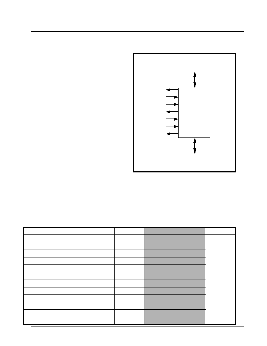
·Á
·Á
·Á
·Á
DS3 UNI FOR ATM
XRT7245
PRELIMINARY
REV. 1.03
175
bytes that contain information on: Path Overhead
Identification, Bit Interleaved Parity Calculation results,
Far-End Block Error status, and stuffing status. The
generation of PLCP frames can either be synchronized
to an external 8 kHz reference clock or to timing from
the Receive PLCP Processor. PLCP frame generation
can also be asynchronous with respect to any timing
signals. The Transmit PLCP Processor can compute
its "nibble-stuffing" requirements based upon its
configured synchronous timing source (e.g., the ex-
ternal 8 kHz reference clock or Receive PLCP
Timing), arbitrarily controlled via an external pin or by
following a fixed stuffing pattern. Once a PLCP frame
is formed, it is routed to the Transmit DS3 Framer
Block of the UNI for transmission to the "Far End" Ter-
minal. Figure 46 presents a simple illustration of the
Transmit PLCP Processor and the associated exter-
nal pins.
Note: The user has the option of taking advantage of the
full DS3 payload bandwidth by by-passing the PLCP
Processor altogether. This option will be referred to as
"Direct Mapping" and is discussed in Section 6.3.3.9
6.3.2
Description of the PLCP Frame and the
Path Overhead (POH) Bytes
The Transmit PLCP Processor receives ATM cells
from the Transmit Cell Processor. It then multiplexes
these cells with some overhead (OH) bytes and
frames this composite information into PLCP Frames.
Table 21 presents the byte format of a PLCP Frame.
F
IGURE
46. S
IMPLE
I
LLUSTRATION
OF
THE
T
RANSMIT
PLCP P
ROCESSOR
B
LOCK
Transmit PLCP
Processor
TxPFrame
8kRef
StuffCtl
TxPOHFrame
TxPOH
TxPOHIns
TxPOHClk
From Transmit Cell
Processor
To Transmit DS3
Framer
T
ABLE
21: F
RAME
F
ORMAT
OF
THE
PLCP F
RAME
PLCP F
RAME
2
BYTES
POI 1
BYTE
POH
1
BYTE
PLCP P
AYLOAD
53
BYTES
13≠14
NIBBLES
A1
A2
P11
Z6
First ATM Cell
A1
A2
P10
Z5
ATM Cell
A1
A2
P9
Z4
ATM Cell
A1
A2
P8
Z3
ATM Cell
A1
A2
P7
Z2
ATM Cell
A1
A2
P6
Z1
ATM Cell
A1
A2
P5
X
ATM Cell
A1
A2
P4
B1
ATM Cell
A1
A2
P3
G1
ATM Cell
A1
A2
P2
X
ATM Cell
A1
A2
P1
X
ATM Cell
A1
A2
P0
C1
Twelfth ATM Cell
Trailer

XRT7245
DS3 UNI FOR ATM
·Á
·Á
·Á
·Á
PRELIMINARY
REV. 1.03
176
Each PLCP frame consists of 12 ATM Cells, 24 bytes
of Frame Alignment patterns (the A1 and A2 bytes),
12 bytes of POI (Path Overhead Identifiers), 12 bytes
of POH (Path Overhead) and a 13 or 14 nibble trailer
which is appended to the PLCP Frame for frequency
justification. Once a PLCP Frame is formed it is rout-
ed to the Transmit DS3 Framer block of the UNI. The
order of transmission of the PLCP frame begins from
the upper left hand corner of the frame (A1 byte), and
proceeds through the frame in a manner similar to
reading this page of text, to the lower right hand cor-
ner (the 13 or 14 nibble trailer).
The definition of each of the overhead bytes within
the PLCP Frame are presented below.
A1, A2 Frame Alignment Pattern Bytes
Each row within a PLCP frame will begin with two
bytes of Frame Alignment patterns which are denoted
as A1 and A2 in Table 21. In accordance with the
ATM Forum UNI spec, the Transmit PLCP Processor
will assign the values: A1 = F6h and A2 = 28h.
POI (Path Overhead Identifier) Bytes: P0-P11
The Path Overhead Identifier (POI) bytes are used to
index the adjacent Path Overhead (POH) bytes, as
tabulated below in Table 22.
The Path Overhead bytes (POH) are defined below.
∑ Z1≠Z6 Bytes: Growth Octets
The Z1≠Z6 octets presently have no particular appli-
cation, and are reserved for future use. The Transmit
PLCP Processor will set these octets to 00h. The
far-end Receive PLCP Processor will ignore the
values contained in these fields.
∑ F1: User Octet
This byte is unused in the UNI and is consequently
programmed to 00h. Therefore, the Far-End Receive
PLCP Processor will ignore the values contained in
the byte-field.
Note: This octet is used in the IEEE 802.6 MAN and in
SMDS applications as a 64 kbps data link channel for
proprietary use by the network provider.
∑ B1≠Bit Interleaved Parity≠8
The B1 byte contains the result of BIP-8 (Bit Inter-
leaved Parity) calculations. The Bit Interleaved Parity
(BIP-8) byte field supports path error monitoring. The
Transmit PLCP Processor will compute the BIP-8 over
a 12 x 54 octet structure, within each PLCP frame.
Specifically, these calculations involve the path over-
head (POH) byte fields and the associated ATM cells
for a total of 648 octets. The resulting BIP-8 value is
inserted into the B1 byte field within the very next
PLCP frame. BIP-8 is an eight bit code in which the
nth bit of the BIP-8 code reflects the even-parity bit
calculated with the nth bit of each octet involved in the
calculation. Thus, the BIP-8 value presents the results
for 8 separate even-bit parity calculations.
T
ABLE
22: POI C
ODE
AND
A
SSOCIATED
POH B
YTES
POI
POI C
ODE
A
SSOCIATED
POH B
YTE
P11
2Ch
Z6
P10
29h
Z5
P9
25h
Z4
P8
20h
Z3
P7
1Ch
Z2
P6
19h
Z1
P5
15h
F1 (Frame)
P4
10h
B1 (BIP-8)
P3
0Dh
G1 (FEBE)
P2
08h
M1
P1
04h
M2
P0
01h
C1 (Stuff Indicator)
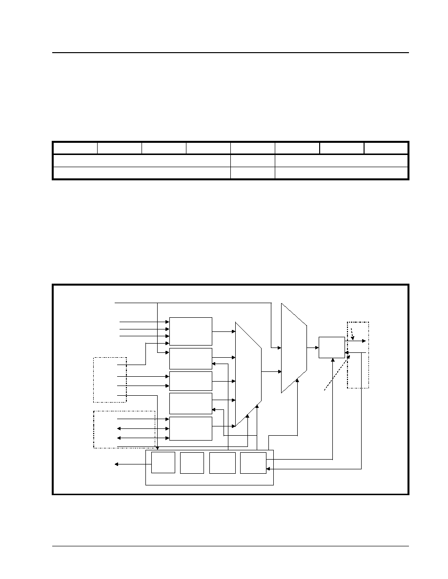
·Á
·Á
·Á
·Á
DS3 UNI FOR ATM
XRT7245
PRELIMINARY
REV. 1.03
177
∑ G1--PLCP Path Status
This byte-field contains some diagnostic information
which was compiled by the "Near-End" Receive
PLCP Processor of this UNI device (See Section
7.2.2.2.2). The purpose of this diagnostic byte field is
to inform the Far-End Terminal of whether or not the
(Near End) Receive PLCP Processor of this UNI has
detected errors or has had problems framing to its (the
Far-End Transmit PLCP Processor's) transmission.
Table 23 presents the bit-format of the G1 octet
which consists of a 4 bit Far-End Block Error (FEBE)
subfield, a 1 bit RAI (Yellow) alarm and 3 X-bits (the
X bits are ignored).
∑ C1--Stuffing Status/Nibble-Trailer Length
Indicator Byte
Table 21 indicates that the PLCP frame will contain a
nibble trailer of either 13 or 14 nibbles, appended to
the end of each PLCP frame. This option of using
either 13 or 14 nibbles presents the Transmit PLCP
processor with a stuff opportunity. This octet (C1)
conveys the nibble stuffing status and is also the
nibble length indicator for the current PLCP frame.
For more information on the C1 octet, please see
Section 6.3.3.1.
6.3.3
Functional Description of the Transmit
PLCP Processor Block
Figure 47 presents a functional block diagram of the
Transmit PLCP Processor.
Figure 47 indicates that the Transmit PLCP Processor
consists of the following functional blocks.
∑
Controlled Stuff Generator, C1 Byte
∑
BIP-8 Generator
∑
G1 Byte Generator
∑
Framing Byte, POI, Dummy POI Generator
T
ABLE
23: B
IT
F
ORMAT
OF
G1 O
CTET
B
IT
7
B
IT
6
B
IT
5
B
IT
4
B
IT
3
B
IT
2
B
IT
1
B
IT
0
Far End Block Error (FEBE)
RAI (Yellow)
X bits (Ignored by the Receiver)
4 Bits
1 Bit
3 Bits
F
IGURE
47. F
UNCTIONAL
B
LOCK
D
IAGRAM
OF
THE
T
RANSMIT
PLCP P
ROCESSOR
Controlled
Stuff Generator
C1 Byte
BIP-8
Generator
G1 Byte
Generator
Framing Bytes,
POI, Dummy
POH Generator
External POH
Collector
Row
Counter
(12)
Stuff
Counter
(13/14)
Column
Counter
(57)
Byte
Clock
Generator
Byte/Nibble
Converter
Over Head
MUX
Over Head
Payload
MUX
To/From
Tx Cell
Processor
StuffCtl
8kRef
TimeRefSel
RxPStuff
RxFEBE
RxYellowAlarm
TxPOH
TxPOHClk
TxPOHFrame
RxPFrame
From
Rx PLCP
TxPOHIns
OH
Address
Timing & Control
From/To
DS3
Framer
Block
Byte Clock
Nibble Clock
TxPFrame
PayLoad/OH
TxNibbleData
TxNibbleClock
To/From
Pins
XRT7245
DS3 UNI FOR ATM
·Á
·Á
·Á
·Á
PRELIMINARY
REV. 1.03
178
∑
External POH Collector
∑
Transmit PLCP Framer
∑
Overhead MUX
∑
Overhead Payload MUX
∑
Byte/Nibble Converter
The role of some of these functional blocks will be
discussed below.
6.3.3.1
Transmit PLCP Frame Timing, Stuff
Control--C1 Byte
The Controlled Stuff Generator portion of the Transmit
PLCP Processor is responsible for three things.
1.
Determining the nibble-stuffing requirements for
the current PLCP frame.
2.
Fulfilling these nibble-stuffing requirements.
3.
Reflecting the nibble-stuffing status in the C1
byte.
Table 24 indicates the Transmit PLCP Processor will
append either a 13 or 14 nibble trailer at the end of
each PLCP frame, in order to frequency justify the
framing to 8 kHz. This choice between 13 or 14 nib-
bles presents the Transmit PLCP Processor with a
"stuff" opportunity.
The Transmit PLCP Processor can be configured into
one of four frame-timing/stuff-control options. The us-
er selects these options by writing the appropriate
data to bit 1 and bit 0 (TimRefSel[1, 0], within the UNI
Operating Mode Register. The bit format of this register
is presented below.
UNI Operating Mode Register: Address = 00h
B
IT
7
B
IT
6
B
IT
5
B
IT
4
B
IT
3
B
IT
2
B
IT
1
B
IT
0
Local Loop-
back
Cell Loop-
back
PLCP Loop-
back
Reset
Direct
Mapped ATM
C-Bit/M13
TimRefSel[1, 0]
R/W
R/W
R/W
R/W
R/W
R/W
R/W

·Á
·Á
·Á
·Á
DS3 UNI FOR ATM
XRT7245
PRELIMINARY
REV. 1.03
179
The values for TimRefSel[1, 0] and the correspond-
ing options are presented in Table 24.
T
ABLE
24: PLCP F
RAME
T
IMING
AND
S
TUFF
C
ONTROL
O
PTIONS
B
IT
1
B
IT
0
R
ESULT
0
0
TimRefSel[1,0] = 00
PLCP Frame Timing Source: Receive PLCP Processor Timing.
In this configuration, the Transmit PLCP Processor takes its timing from the Receiver Start of
Frame signal (from the Receive PLCP Processor, within the UNI) to start a PLCP frame. The
Transmit PLCP Processor will also use this signal to calculate stuff opportunities.
Stuff Control: The Transmit PLCP Framer has a stuff-opportunity that occurs once every three
PLCP frames. Therefore, the stuff-control algorithm is based on a repeating "Stuff-Control" cycle
that consists of these three (3) PLCP cycles (or a 375µs interval). The three composite PLCP
frames of a stuff control cycle, when TimRefSel[1, 0] = 00, is presented below.
PLCP Frame 1 (the first of the 3 frames) will contain 13 trailer nibbles. The C1 byte, within this
PLCP frame, will contain the value FFh. This value identifies the current PLCP Frame as
Frame #1 in this 3 Frame Cycle, and informs the Far-End Receive PLCP Processor that the
trailer length is 13.
PLCP Frame 2 (the second of the 3 frames) will contain 14 trailer nibbles. The C1 byte, within
this PLCP frame, will contain the value 00h. This value identifies the current PLCP Frame as
Frame #2 in this 3 Frame Cycle, and informs the Far-End Receive PLCP Processor that the
trailer nibble length is 14.
PLCP Frame 3 (the last of the 3 frames) will contain either 13 or 14 trailer nibbles, depending
upon the calculated stuffing requirements. Hence, the Transmit PLCP can generate two versions
of Frame #3, "No Stuff" Frame #3 and "Stuff" Frame #3.
"No Stuff" Frame #3: If the Transmit PLCP Processor has determined that no stuff is required
then it will append only 13 trailer nibbles at the end of the current PLCP frame. The C1 byte,
within this PLCP frame, will identify the current frame as a "No Stuff" Frame #3, in the 3 Frame
cycle, by carrying the value 66h.
"Stuff" Frame #3: If the Transmit PLCP Processor has determined that a stuff is required,
then it will append 14 trailer nibbles at the end of the current PLCP frame. The C1 byte, within
this PLCP frame, will identify the current frame as a "Stuff" Frame #3, in the 3 Frame cycle, by
carrying the value 99h.
Once the Stuff Control algorithm has processed through PLCP Frame #3, the Transmit PLCP
Processor will proceed to generate a PLCP Frame #1, and repeat this 3 frame cycle.
0
1
TimRefSel[1,0] = 01
PLCP Frame Timing Source: External 8 kHz Clock Signal
In this configuration, the Transmit PLCP Processor takes its timing from an 8 kHz signal which
is applied at the 8KRef input pin. The Transmit PLCP Processor will also use this signal to cal-
culate stuff opportunities.
Stuff Control: As mentioned earlier, a stuff opportunity for the Transmit PLCP Processor
occurs once in a period of three (3) PLCP Frames. These composite PLCP frames and the
resulting C1 values are the same as presented in the above "PLCP Frame Timing/Stuff Con-
trol" Option (TimRefSel = 00).
1
0
TimRefSel[1,0] = 10; - StuffCtl Input Pin
PLCP Frame Timing Source: PLCP Frame timing is asynchronous upon power up or reset.
In this configuration, the Transmit PLCP Processor will start PLCP frames based upon an
asynchronous timing signal. The stuffing opportunities are not computed based on this timing,
but on the logic state of an input pin.
XRT7245
DS3 UNI FOR ATM
·Á
·Á
·Á
·Á
PRELIMINARY
REV. 1.03
180
Note: The selection of these bits also affects the operation
of the Transmit DS3 Framer. This subject is presented in
Section 6.4.3.4. In all cases, the C1 byte of each PLCP
frame will reflect the stuffing phase and number of trailer
nibbles that are appended to the current PLCP frame.
Stuff Control: The Stuff Control algorithm is controlled by the logic state of the external pin,
StuffCtl.
As with the previous two Stuff Control options, the Transmit PLCP Framer has a stuff-opportunity
that occurs once every three PLCP frames. Each of these composite PLCP frames are dis-
cussed below.
∑ PLCP Frame 1 (the first of the 3 frames) will contain 13 trailer nibbles. The C1 byte, within
this PLCP frame, will identify the current frame as a Frame #1, by carrying the value FFh.
Note this frame will be created independent of the state of the StuffCtl pin.
∑ PLCP Frame 2 (the second of the 3 frames) will contain 14 trailer nibbles. The C1 byte,
within this PLCP frame, will identify the current frame as a Frame #2, by carrying the value
00h. Note this frame will be created independent of the state of the StuffCtl pin.
∑ PLCP Frame 3 (the last of the 3 frames) will contain either 13 or 14 trailer nibbles, depending
upon the logic state of the "StuffCtl" input pin. Therefore, the Transmit PLCP can generate one
of two versions of Frame #3: "No Stuff" Frame #3 and "Stuff" Frame #3.
StuffCtl = "0"--No Stuff" Frame #3: If the StuffCtl pin is "low" then the Transmit PLCP pro-
cessor will generate a "No Stuff" Frame #3. This PLCP frame will contain 13 trailer nibbles. The
C1 byte will identify the current PLCP frame as a "No Stuff" Frame #3 by carrying the value 66h.
StuffCtl = "1"--"Stuff" Frame #3: If the StuffCtl pin is "high" then the Transmit PLCP Processor
will generate a "Stuff" Frame #3. This PLCP frame will contain 14 trailer nibbles. The C1 byte
will identify the current PLCP frame as a "Stuff" Frame #3 by carrying the value 99h.
1
1
TimRefSel[1,0] = 11; - Fixed Stuffing Pattern
PLCP Frame Timing: Asynchronous upon power on.
Stuff Control: The Transmit PLCP Processor will use a fixed Stuffing Pattern which is con-
trolled by an internal counter. This stuffing pattern results in the transmission of 13, 14, 13, 13,
14, 14, 13, 14, 14 trailer nibbles in every 9 PLCP frames repeatedly. This corresponds to 8000 -
1.5 x 10
-5
Hz when a perfect 44.736 MHz is used as the transmit clock. Table 25 lists the con-
tents of the C1 bytes for each of these 9 PLCP Frames.
T
ABLE
24: PLCP F
RAME
T
IMING
AND
S
TUFF
C
ONTROL
O
PTIONS
(C
ONT
'
D
)
B
IT
1
B
IT
0
R
ESULT
T
ABLE
25: V
ALUE
OF
C1
FOR
THE
9 PLCP F
RAMES
,
WHEN
THE
F
IXED
S
TUFFING
O
PTION
IS
S
ELECTED
PLCP F
RAME
N
UMBER
N
UMBER
OF
T
RAILER
N
IBBLES
IN
F
RAME
C1 B
YTE
V
ALUE
1
13
FFh
2
14
00h
3
13
66h
4
13
FFh
5
14
00h
6
14
99h
7
13
FFh
8
14
00h
9
14
99h
·Á
·Á
·Á
·Á
DS3 UNI FOR ATM
XRT7245
PRELIMINARY
REV. 1.03
181
6.3.3.2
BIP-8 Generator--B1 Byte
The BIP-8 (Bit Interleaved Parity) generator takes a
total of 12 x 54 octets per PLCP frame, (which con-
sists of the POH byte fields and the associated ATM
cells--a total of 648 octets) and performs a very
specific sequence of calculations. The BIP-8 generator
takes bit 7 (the MSB) of each of the 648 octets and
calculates an even parity bit (based upon these 648
MSB bits). The resulting parity bit is inserted into bit 7
of the B1 byte. This same calculation is also performed
for each of the remaining 7 bits in each octet. The re-
sulting parity bits are grouped together and inserted
into the B1 byte field. Therefore, the content of the B1
byte is the result of 8 separate parity bit calculations.
The BIP-8 Calculation results that are obtained based
upon the data within a given PLCP frame, will be in-
serted into the B1 octet position of the very next
PLCP frame.
The B1 byte will ultimately be used by the "Far-End"
Receive PLCP Processor, in order to monitor the
transmission performance between the "Near-End"
Transmitter and the "Far-End" Receiver. For more in-
formation on how the Receive PLCP Processor han-
dles the B1 byte, please see Section 7.2.2.3.1.
6.3.3.3
G1 Byte Generator
The purpose of the G1 byte is to provide the "Far-End"
Transmitter with diagnostic information on how well
the "Near-End" Receive PLCP (e.g., the on-chip Re-
ceive PLCP) Processor is receiving and processing its
PLCP frames. The bit field of the G1 byte is
presented below.
Each of these bit-fields are discussed below.
Far-End Block Error (FEBE)
The Receive PLCP Processor will receive and extract
the PLCP Overhead bytes from incoming PLCP
frames, originating from a "Far-End" Transmit PLCP
Processor. While the Receive PLCP Processor is re-
ceiving a PLCP frame, it will calculate its own BIP-8
value for that frame. Afterwards, the Receive PLCP
Processor will then compare its BIP-8 value with the
contents of the B1 byte that it extracts from the very
next PLCP frame. If these two BIP-8 values match,
then the Receive PLCP Processor will reflect this fact
by writing a FEBE value of 0h into a G1 byte. At
some phase during PLCP frame processing, the Re-
ceive PLCP Processor will route the contents of the
G1 byte to the Transmit PLCP Processor (on the
same chip). This G1 byte will be packed in the next
outbound PLCP frame, which is in turn routed to the
Transmit DS3 Framer. The G1 byte is ultimately
transmitted to the "Far-End" Receive PLCP Processor
over the DS3 transport medium, where it will be
processed and evaluated.
If the Receive PLCP Processor determines that the
two BIP-8 values do not match, then the Receive
PLCP Processor will count the number of bit-errors
(e.g., the number of bit-by-bit discrepancies between
these two BIP-8 values) and write this value into the
FEBE nibble of the G1 byte. This G1 Byte will be
routed to the Transmit PLCP Processor, inserted into
the next outbound PLCP frame, and received and
processed by the Far-End Receive PLCP Processor,
as described above.
Note:
1. Since the BIP-8 value only contains 8-bits, the largest
number of errors that the Receive PLCP processor
can detect is "8". Therefore, the "FEBE" nibble-field,
within the G1 byte must not contain a value
exceeding the number "8".
2. For more information on how the Receive PLCP
Processor handles the G1 byte, from the Far-End
Transmit PLCP Processor, please see Section
7.2.2.2.2.
RAI (Yellow Alarm)
If the Receive PLCP Processor has had sufficient
trouble framing to the incoming PLCP frames, (e.g.,
if the Receive PLCP remains "Un-framed" for 2 to 10
seconds), then the Receive PLCP Processor will as-
sert the RAI bit in the G1 byte. The contents of
the G1 byte will be routed to the Transmit PLCP
Processor and subjected to the processing that was
described above.
6.3.3.4
Inserting Errors into the PLCP Path
Overhead Bytes
The XRT7245 DS3 UNI has provision to allow the us-
er to insert errors into the POH bytes of each out-
bound PLCP frames. The user may wish to do this for
chip/equipment test purposes.
The following sections briefly discuss these options.
B
IT
7
B
IT
6
B
IT
5
B
IT
4
B
IT
3
B
IT
2
B
IT
1
B
IT
0
Far End Block Error (FEBE)
RAI (Yellow)
X Bits (Ignored by the Receiver)
4 Bits
1 Bit
3 Bits
XRT7245
DS3 UNI FOR ATM
·Á
·Á
·Á
·Á
PRELIMINARY
REV. 1.03
182
6.3.3.4.1
Inserting Errors into the B1 Byte
There are occasions when the user may wish to in-
ject errors into the B1 byte of the PLCP frame in or-
der to verify that the Far-End Receiving hardware is
functioning properly and will detect these errors and
respond accordingly. The UNI allows the user to in-
ject these errors into the B1 byte via the TxPLCP
BIP-8 Error Mask Register, as depicted below.
The B1 (BIP-8) byte of a PLCP frame is always XORed
with this mask byte. The results of this operation are
written back into the B1-byte position, prior to trans-
mission. The user can insert an error into a particular
bit of a B1 byte, by writing a "1" into the corresponding
bit in this register.
Note: This register must be 00h for normal operation. This
register is of value 00h following power up or reset.
6.3.3.4.2
Inserting Errors into the A1, A2 Bytes
The UNI allows the user to insert errors into each of
the "Frame Alignment" bytes A1 and A2. The user
can insert these errors by writing the appropriate da-
ta to the "Tx PLCP A1 Byte Error Mask Register (Ad-
dress = 48h); and the "Tx PLCP A2 Byte Error Mask
Register (Address = 49h). The bit formats of these two
registers follows.
The UNI IC automatically takes each A1 byte from
within an outbound PLCP frame, and performs an
XOR operation with the contents of the "Tx PLCP A1
Byte Error Mask" Register. The results of this opera-
tion are written back into the A1 Byte fields of the
PLCP frame, prior to transmission.
The UNI IC also performs the same set of operations
on the A2 bytes of the PLCP frame, with the "Tx PLCP
A2 Byte Error Mask" register.
Therefore, if the user does not wish to insert errors
into the A1 and A2 byte fields of each outbound PLCP
frame, he/she must insure that these two registers
contain the value 00h (the default value).
6.3.3.5
Manipulating the FEBE-Nibble Field
within the G1 Bytes
The UNI allows the user to either transmit G1 bytes
with a FEBE value of `0h', or to transmit a G1 byte with
the correct FEBE count, as determined by the "Near-
End" Receive PLCP Processor.
The user can exercise this option by writing the ap-
propriate data to bit 4 of the Tx PLCP G1 Byte Register
(Address = 4Bh). The bit-format of this register is
presented below.
Tx PLCP BIP-8 Error Mask Register, Address = 4Ah
B
IT
7
B
IT
6
B
IT
5
B
IT
4
B
IT
3
B
IT
2
B
IT
1
B
IT
0
B1 Error Mask
R/W
R/W
R/W
R/W
R/W
R/W
R/W
R/W
Tx PLCP A1 Byte Error Mask Register (Address = 48h)
B
IT
7
B
IT
6
B
IT
5
B
IT
4
B
IT
3
B
IT
2
B
IT
1
B
IT
0
A1 Error Mask
0
0
0
0
0
0
0
0
Tx PLCP A2 Byte Error Mask Register (Address = 49h)
B
IT
7
B
IT
6
B
IT
5
B
IT
4
B
IT
3
B
IT
2
B
IT
1
B
IT
0
A2 Error Mask
0
0
0
0
0
0
0
0
·Á
·Á
·Á
·Á
DS3 UNI FOR ATM
XRT7245
PRELIMINARY
REV. 1.03
183
Writing a `1' to this bit-field will cause the Transmit
PLCP Processor to transmit G1 bytes with the FEBE
nibble value of `0h' (independent of the number of
BIP-8 errors detected by the Receive PLCP Processor).
Writing a `0' to this bit-field will cause the Transmit
PLCP Processor to transmit G1 bytes with the
correct FEBE count, as determined by the "Near-
End" Receive PLCP Processor.
6.3.3.6
Forcing a Yellow Alarm--Via Software
Control
The UNI allows the user to generate a "Yellow Alarm
(PLCP Version thereof)" via software control. In this
case, the Transmit PLCP Processor will generate a
"Yellow Alarm" by automatically setting the "RAI" bit
within each G1 byte to `1'. The user can exercise this
option by writing the appropriate bit to bit-field 3 of
the Tx PLCP G1 Byte Register (Address = 4Bh). The
bit format of this register follows.
Writing a `1' to this bit-field forces the "PLCP--Yellow
Alarm" condition. Writing a `0' to this bit-field allows
the state of the RAI bit to be based upon the framing
conditions of the "Near-End" Receive PLCP Processor.
6.3.3.7
Transmitting Data Link Messages
via the G1 Byte
The "Tx PLCP G1 Byte" Register contains three bit-
fields that can be used to support a 24 kbps data link
between the Near-End Transmit PLCP Processor,
and the Far-End Receive PLCP Processor, as depicted
below.
Whatever data is written into the three bit-fields will
appear in Bits 2≠0 of the incoming G1 byte at the Far-
End Receive PLCP Processor.
6.3.3.8
Inserting POH Bytes via the TxPOH
Serial Input Port
The UNI allows the user to externally insert his/her
own PLCP POH (Path Overhead) bytes via a serial
input interface consisting of the pins: TxPOHIns, Tx-
POH, TxPOHFrame, and TxPOHClk. The user can
activate this serial input port by asserting the TxPO-
HIns input pin (e.g., setting it "high"). When this pin is
"low", the UNI will internally generate the POH bytes.
However, when this pin is "high", the user will be ex-
pected to provide his/her own value for the POH
bytes via the TxPOH input pin. The UNI will assert
(toggle "high") the TxPOHFrame output pin when it
expects the MSB of the Z6 byte. The user will be ex-
pected to provide his/her value for the Z6 byte, with
the MSB first, in descending order. Immediately after
the LSB of the Z6 byte, the TxPOH Serial Input port
will be expecting the MSB of the Z5 byte, and so on.
The byte order that this serial input port expects is as
presented in Table 24. Once the TxPOH serial input
port has read in the LSB of the C1 byte, it will repeat
this sequence of bytes, beginning with the Z6 byte
first. The POH data will be serially latched into the
TxPOH input on the rising edge of the TxPOHClk
Tx PLCP G1 Byte Register (Address = 4Bh)
B
IT
7
B
IT
6
B
IT
5
B
IT
4
B
IT
3
B
IT
2
B
IT
1
B
IT
0
Unused
TxPLCP FEBE Mask
Yellow Alarm
LSS(2)
LSS(1)
LSS(0)
RO
RO
RO
R/W
R/W
R/W
R/W
R/W
Tx PLCP G1 Byte Register (Address = 4Bh)
B
IT
7
B
IT
6
B
IT
5
B
IT
4
B
IT
3
B
IT
2
B
IT
1
B
IT
0
Unused
TxPLCP FEBE Mask
Yellow Alarm
LSS(2)
LSS(1)
LSS(0)
RO
RO
RO
R/W
R/W
R/W
R/W
R/W
Tx PLCP G1 Byte Register (Address = 4Bh)
B
IT
7
B
IT
6
B
IT
5
B
IT
4
B
IT
3
B
IT
2
B
IT
1
B
IT
0
Unused
TxPLCP FEBE Mask
Yellow Alarm
LSS(2)
LSS(1)
LSS(0)
RO
RO
RO
R/W
R/W
R/W
R/W
R/W
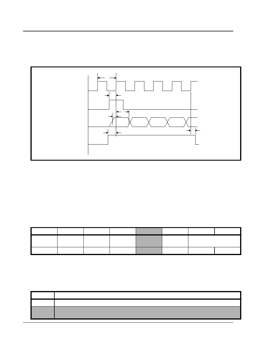
XRT7245
DS3 UNI FOR ATM
·Á
·Á
·Á
·Á
PRELIMINARY
REV. 1.03
184
output signal. The clock rate of the TxPOHClk signal
is nominally 768 kHz.
Figure 48 presents a timing diagram depicting the
behavior of the signals associated with the TxPOH
serial input interface during its use.
The TxPOH Serial Input Port also allows the user to
externally insert their POH bytes selectively (e.g.,
some POH bytes are internally generated, others are
externally inserted). This can be accomplished by as-
serting the TxPOHIns and inserting data into the Tx-
POH input at a time when the TxPOH input is expect-
ing this data, per the byte/bit order described above.
If the user wishes to allow the remainder of the data
to be "internally" generated, he/she must negate the
TxPOHIns pin during the time-slot periods for those
POH bytes.
6.3.3.9
The "Direct Mapped ATM" Option
The UNI allows the user to disable (or by-pass) the
Transmit PLCP processor and to directly insert the
ATM cells, from the Transmit Cell Processor into the
DS3 payload. The user can exercise this option by
writing to Bit 3 of the UNI Operating Mode Register,
as depicted below.
The following table presents the relationship between
the value of this bit and the type of ATM Mapping in-
corporated.
F
IGURE
48. A
N
I
LLUSTRATION
OF
THE
B
EHAVIOR
OF
THE
T
X
POH S
ERIAL
I
NTERFACE
SIGNALS
DURING
U
SER
I
NPUT OF
POH D
ATA
.
TxPOHFrame
TxPOH
TxPOHIns
TxPOHClk
t19
t20
t21
t23
t22
t18
UNI Operating Mode Register: Address = 00h
B
IT
7
B
IT
6
B
IT
5
B
IT
4
B
IT
3
B
IT
2
B
IT
1
B
IT
0
Local
Loopback
Cell
Loopback
PLCP
Loopback
Reset
Direct
Mapped ATM
C-Bit/M13
TimRefSel[1, 0]
R/W
R/W
R/W
R/W
R/W
R/W
R/W
T
ABLE
26: T
HE
R
ELATIONSHIP
BETWEEN
B
IT
3
OF
THE
UNI O
PERATING
M
ODE
R
EGISTER
AND
THE
R
ESULTING
"ATM C
ELL
" M
APPING
M
ODE
.
B
IT
3
M
APPING
M
ODE
0
PLCP Mode: The PLCP is enabled. PLCP Frames will be mapped into the "outbound" DS3 Frame
1
Direct-Mapped ATM Mode:
The PLCP Processor block is bypassed. ATM cells will be directly mapped into
the "outbound" DS3 Frame
·Á
·Á
·Á
·Á
DS3 UNI FOR ATM
XRT7245
PRELIMINARY
REV. 1.03
185
Final Notes about the Transmit PLCP Processor
The Transmit PLCP Processor will be disabled, upon
power up or reset. Therefore, the user must write a
"1" to this bit in order to enable the PLCP Processor.
Selection of this bit affects both the Transmit PLCP
Processor and the Receive PLCP Processor.
The advantage of selecting the "Direct-Mapped ATM"
option is to result in a more efficient use of the DS3
Bandwidth. This is because in the Direct Mapped
ATM mode, the user is not required to include all of
the POH bytes that must be included in PLCP frames.
The Transmit PLCP Processor will inform the external
circuitry that a PLCP frame has been assembled and
transmitted out of the PLCP Processor by pulsing the
TxPFrame output pin `high' during the transmission of
the last trailer nibble.
6.4
Transmit DS3 Framer
6.4.1
Brief Description of the Transmit
DS3 Framer
The Transmit DS3 Framer takes the incoming data,
which can be either PLCP frames from the Transmit
PLCP Processor or ATM Cells from the Transmit Cell
Processor and maps it into the payload portion of the
DS3 frame. The Transmit DS3 Framer supports either
the M13 or C-Bit Parity frame formats. The Transmit
DS3 Framer operates at 44.736 MHz and framing is
derived from an input clock signal. The framing over-
head bits are generated and inserted with the DS3
payload bits to make up the complete DS3 frame. The
DS3 frame is then encoded into either the Unipolar, AMI
or B3ZS line codes. When the Transmit DS3 Framer is
operating in the C-Bit Parity Framing format, it provides
an interface that supports the transmission of path
maintenance data link messages on the outgoing DS3
frames via the on-chip LAPD Transmitter. The Transmit
DS3 Framer also includes an on-chip Transmit FEAC
Processor that supports the transmission of FEAC (Far
End Alarm and Control) messages over the outgoing
DS3 frame. Different transmission conditions like AIS
(Alarm Indication Signal), Idle Condition and the Yellow
Alarm can be generated upon software command.
Further, the LOS (Loss of Signal) condition can be
simulated upon software command.
6.4.2
Detailed Functional Description of the
Transmit DS3 Framer
The Transmit DS3 Framer receives PLCP frames
from the Transmit PLCP block, or ATM Cells from the
Transmit Cell Processor, and inserts this data into the
payload portion of each outbound DS3 frame. The
Transmit DS3 Framer proceeds to generate the over-
head (OH) bits and interleave these bits with the DS3
payload bits to form the complete DS3 data stream.
The Transmit DS3 Framer will then encode this DS3
Frame Data into a Unipolar Format (for transmission
over optical fiber) or in a Bipolar format (AMI or B3ZS
line code) for transmission over a transformer coupled
copper medium, to a far away DS3 Receiver Terminal
via an LIU IC.
The Transmit DS3 Framer also provides a serial input
port to allow the user to insert his/her own OH bits in-
to the outbound DS3 Frame. Finally, the Transmit
DS3 Framer allows the user to insert errors into the
Framing Bits or transmit various alarm conditions via
software control in order to support equipment testing
as well as transmitting the appropriate alarm signals
as conditions warrant.
Figure 49 presents a simple illustration of the Transmit
DS3 Framer block, along with the associated external
pins.
Figure 49 presents a functional block diagram of the
Transmit DS3 Framer block.
F
IGURE
49. A S
IMPLE
I
LLUSTRATION
OF
THE
T
RANSMIT
DS3 F
RAMER
B
LOCK
AND
THE
ASSOCIATED
E
XTERNAL
P
INS
TxPOS
TxNEG
Transmit
DS3
Framer
TxFrame
TxOHClk
TxLineClk
TxAISEn
TxFrameRef
TxInClk
TxOHIns
TxOH
From Transmitter PLCP
Processor
To DS3 Line Interface Unit
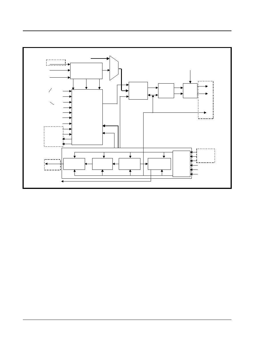
XRT7245
DS3 UNI FOR ATM
·Á
·Á
·Á
·Á
PRELIMINARY
REV. 1.03
186
Figure 50 indicates that the Transmit DS3 Framer
consists of the following functional blocks.
∑
Overhead Generator
∑
Programmable Pattern Generator (PPG)
∑
Payload/PPG MUX
∑
Payload/OH MUX
∑
B3ZS Encoder
∑
LOS Generator
∑ Timing and Control
Some of these functional blocks will be discussed in
some of the next few sections.
6.4.3
Description of the DS3 Frames and
Associated Overhead Bits
The role of the various OH (overhead) bits are best
described by discussing the DS3 Frame Format as a
whole. The DS3 Frame contains 4760 bits, of which
56 bits are overhead and the remaining 4704 bits are
"payload" bits. PLCP Frames or "Direct-Mapped" ATM
cells are inserted into this 4704 bit payload portion,
for each frame. The "payload" data is formatted into
packets of 84 bits and the overhead (OH) bits are in-
serted between these payload packets. The
XRT7245 UNI device supports the following two DS3
framing formats:
∑
C-bit Parity
∑ M13
Table 27 and 28 present the DS3 Frame Format for
C-bit Parity and M13, respectively.
F
IGURE
50. A F
UNCTIONAL
B
LOCK
D
IAGRAM
OF
THE
T
RANSMIT
DS3 F
RAMER
B
LOCK
Programmable Pattern
Generator
Overhead Generator
X, P, M, F, AIC, Na,
FEAC,CP, FEBE, DL,
UDL
Nibble/Serial
Converter
(5 Bit Shift
Register)
B3ZS
Encoder
LOS
Generator
TxAISIn
TxAIS
TxIdle
CBit
Control
CPBit
Control
XBit
Control
TxNibbleData
(from TxPLCP)
TxPOS
TxNEG
Frame Counter
(Divide by 7)
Sub Frame
Counter
(Divide by 8)
Packet Counter
(Divide by 85)
Nibble Counter
(Divide by 4)
Clock &
FrameRef
Selection
Timing & Control
Clock
Reset (Synchronous)
TxFrame
TxOHFrame
TxOHClk
TxOHIns
TxOH
TxLAPDConf
TxFEACConf
F.M.P. Mask
Tx Config
RxOOF
RxAIS
RxLOS
TestMode
TxFrameRef
TxInClk
UNI Control
RxFrame
RxLineClk
TxLineClk
TxNibbleClk
(to TxPLCP)
OH Address
TxLOS
TxOHClk
Payload/PPG
MUX
TxLineClk
from
Rx
Framer
·Á
·Á
·Á
·Á
DS3 UNI FOR ATM
XRT7245
PRELIMINARY
REV. 1.03
187
X = Signaling bit for network control
I = Payload Information (84 bit packets)
Fi = frame synchronization bit with logic value i
P = parity bit
Mi = multiframe synchronization bit with logic value i
AIC = application identification channel
NA = reserved for network application
FEAC = far end alarm and control
DL = data link
CP = C-bit parity
FEBE = far end block error
UDL = User Data Link
T
ABLE
27: DS3 F
RAME
F
ORMAT
FOR
C-
BIT
P
ARITY
.
X
I
F1
I
AIC
I
F0
I
NA
I
F0
I
FEAC
I
F1
I
X
I
F1
I
UDL
I
F0
I
UDL
I
F0
I
UDL
I
F1
I
P
I
F1
I
CP
I
F0
I
CP
I
F0
I
CP
I
F1
I
P
I
F1
I
FEBE
I
F0
I
FEBE
I
F0
I
FEBE
I
F1
I
M0
I
F1
I
DL
I
F0
I
DL
I
F0
I
DL
I
F1
I
M1
I
F1
I
UDL
I
F0
I
UDL
I
F0
I
UDL
I
F1
I
M0
I
F1
I
UDL
I
F0
I
UDL
I
F0
I
UDL
I
F1
I
XRT7245
DS3 UNI FOR ATM
·Á
·Á
·Á
·Á
PRELIMINARY
REV. 1.03
188
X = Signaling bit for network control
I = Payload Information (84 bit packets)
Fi = frame synchronization bit with logic value i
Cij = jth stuff code bit of ith channel
P = parity bit
Mi = multiframe synchronization bit with logic values i
T
ABLE
28: DS3 F
RAME
F
ORMAT
FOR
C-
BIT
P
ARITY
X
I
F1
I
C11
I
F0
I
C12
I
F0
I
C13
I
F1
I
X
I
F1
I
C21
I
F0
I
C22
I
F0
I
C23
I
F1
I
P
I
F1
I
C31
I
F0
I
C32
I
F0
I
C33
I
F1
I
P
I
F1
I
C41
I
F0
I
C42
I
F0
I
C43
I
F1
I
M0
I
F1
I
C51
I
F0
I
C52
I
F0
I
C53
I
F1
I
M1
I
F1
I
C61
I
F0
I
C62
I
F0
I
C63
I
F1
I
M0
I
F1
I
C71
I
F0
I
C72
I
F0
I
C73
I
F1
I
·Á
·Á
·Á
·Á
DS3 UNI FOR ATM
XRT7245
PRELIMINARY
REV. 1.03
189
The user can choose between these two frame formats,
by writing the appropriate data to bit 2 of the UNI
Operating Mode Register (Address = 00h), as
depicted below.
The following table lists the relationship between the
value of the this bit-field and the resulting DS3 Frame
Format.
The Transmit DS3 Framer will be operating in the
C-Bit Parity frame format, upon power up or reset.
Therefore, the user must write a "1" to this bit field
in order to configure the Framer to operate in the
M13 Mode.
Note: This bit setting also configures the frame format for
the Receive DS3 Framer block as well.
Each of the two DS3 Frame Formats, as presented in
Tables 27 and 28 constitute an M-frame (or a full DS3
Frame). Each M-frame consists of 7-680 bit F-frames
(sometimes referred to as, subframes). In Tables 27
and 28, each F-frame is represented by the individual
rows of payload and OH bits. Each F-frame can be
further divided into 8 blocks of 85 bits, with 84 of the
85 bits available for payload information and the
remaining one bit used for frame overhead.
Differences Between the M13 and C-Bit Parity
Frame Formats
The frame formats for M13 and C-bit Parity are very
similar. However, the main difference between these
two framing formats is in the use of the C-bits. In the
M13 Format, the C-bits reflect the status of stuff-op-
portunities that either were or were not used while
multiplexing the 7 DS2 signals into this DS3 signal. If
two of the three stuff bits, within a F-frame, are "1",
then the associated stuff bit, Si (not shows in Table
28), is interpreted as being a stuff bit. In the C-bit
Parity framing format, the "C" bits take on different
roles, as presented in TTable 30.
UNI Operating Mode Register: Address = 00h
B
IT
7
B
IT
6
B
IT
5
B
IT
4
B
IT
3
B
IT
2
B
IT
1
B
IT
0
Local
Loopback
Cell
Loopback
PLCP
Loopback
Reset
Direct
Mapped ATM
M13/C-Bit*
TimRefSel[1, 0]
R/W
R/W
R/W
R/W
R/W
R/W
R/W
T
ABLE
29: T
HE
R
ELATIONSHIP
BETWEEN
THE
CONTENT
OF
B
IT
2, (C-B
IT
P
ARITY
*/M13)
WITHIN
THE
UNI O
PERATING
M
ODE
R
EGISTER
AND
THE
RESULTING
DS3 F
RAMING
F
ORMAT
B
IT
2
DS3 F
RAME
F
ORMAT
0
C-Bit Parity
1
M13
T
ABLE
30: C-
BIT
F
UNCTIONS
FOR
THE
C-
BIT
P
ARITY
DS3 F
RAME
F
ORMAT
C-B
IT
F
UNCTION
OF
C-
BITS
WHILE
IN
THE
C-B
IT
P
ARITY
F
RAMING
F
ORMAT
C11
AIC (C-Bit Parity Mode)
C12
NA (Reserved for Network Application)
C13
FEAC (Far End Alarm & Control)
C21, C22, C23
User Data Link (undefined for DS3 Frame)
C31, C32, C33
C-bit Parity bits
C41, C42, C43
FEBE (Far End Block Error) Indicators
C51, C52, C53
Path Maintenance Data Link
C61, C62, C63, C71, C72, C73
User Data Link (undefined for DS3 Frame)

XRT7245
DS3 UNI FOR ATM
·Á
·Á
·Á
·Á
PRELIMINARY
REV. 1.03
190
Definition of the DS3 Frame Overhead Bits
In general, the DS3 Frame Overhead Bits serve the
following three purposes:
1.
Support Frame Synchronization between the
Near-End and Far-End DS3 Terminals
2.
Provide parity bits in order to facilitate perfor-
mance monitoring and error detection.
3.
Support the transmission of Alarms, Status, and
Data Link information to the Far-End DS3 Terminal.
The OH bits supporting each of these purposes are
further defined below.
6.4.3.1
Frame Synchronization Bits (Applies
to both M13 and C-bit Parity Framing
Formats)
Each DS3 Frame (M-frame) contains a total of 31 bits
that support frame synchronization. Each DS3 M-frame
contains three M-bits. According to Tables 27 and 28,
these M-bits are the first bits in F-frames 5, 6 and 7.
These three bits appear in each M-frame with the re-
peating pattern of "010". This fact is also presented in
Tables 27 and 28, which contains bit-fields that are
designated as: M0, M1, and M0 (where M0 = "0", and
M1 = "1").
Each F-frame contains four F-bits; which also aid in
synchronization between the Near-end and Far-end
DS3 terminals. Therefore, each DS3 M-frame consists
of a total of 28 F-bits. These F-bits exhibit a repeating
pattern of "1001" within each F-frame. This fact is al-
so presented in Tables 27 and 28, which contains bit-
fields that are designated as: F1, F0, F0, and F1
(where F0 = "0", and F1 = "1").
Each of these bit-fields will be used by the Receive
DS3 Framer, in order to perform Frame Acquisition
and Frame Maintenance functions. For more informa-
tion on how the Receive DS3 Framer uses these bit-
fields, please see Section 7.1.2.2.
6.4.3.2
Performance Monitoring Bits (Parity)
The DS3 Frame uses numerous bit fields to support
performance monitoring of the transmission link be-
tween the Transmit DS3 Framer and the "Far-End"
Receive DS3 Framer. The DS3 frame can contain
two types of parity bits, depending upon the framing
format chosen. P-bits are available in both the M13
and C-bit Parity Formats. However, the C-bit Parity
format also includes additional "C-Parity" bits. In the
XRT7245 DS3 UNI, the C-Parity bit-fields are not
used nor processed by the Receive DS3 Framer.
Therefore, they will not be discussed any further.
P-Bits (Applies to M13 and C-Bit Parity Frame
Formats)
Each DS3 M-frame consists of two (2) P-bits. These
two P-bits carry the parity information of the previous
DS3 frame for performance monitoring. These two P-
bits must be identical, within a given DS3 frame. The
Transmit DS3 Framer will compute the even parity
over all 4704 payload bits in a DS3 frame, and insert
the resulting parity information in the P-bit fields of
the very next DS3 frame. The two P-bits are set to "1"
if the payload of the previous DS3 frame consists of
an odd number of "ones" in the frame. Conversely, the
two P-bits are set to zero if an even number of "ones"
is found in the payload of the previous DS3 frame. For
information on how the Receive DS3 Framer handles
P-bits, please see Section 7.1.2.4.1.
6.4.3.3
Alarm-, Signaling-Related
Overhead Bits
Alarm Indication Signal (AIS) Detection (C-Bit
Parity Framing Format only)
The Alarm Indication Signal (AIS) pattern is a main-
tenance signal that is inserted into the "outbound"
DS3 stream when a failure is detected by the "Near-
End" Receiver. The Transmit DS3 Framer will generate
the AIS pattern as defined in ANSI.T1.107a-1990,
which is described as follows.
∑
Valid M-bits, F-bits, and P-bits
∑
All C-bits are zeros
∑
All X-bits are set to "1"
∑ A repeating "1010..." pattern is written into the pay-
load of the DS3 frames.
Consequently, no ATM cell data will be transmitted
while the Transmit DS3 Framer is transmitting an AIS
pattern.
IDLE Condition Signal
The IDLE Condition signal is used to indicate that the
DS3 channel is functionally sound, but has not yet
been assigned any traffic. The Transmit DS3 Framer
will transmit the IDLE Condition signal as defined in
ANSI T1.107a-1990, which is described as follows.
∑
Valid M-bits, F-bits, and P-bits
∑
The three CP-bits (F-frame #3) are zeros
∑
The X-bits are set to "1"
∑
A repeating "1100.." pattern is written into the pay-
load of the DS3 frames.
·Á
·Á
·Á
·Á
DS3 UNI FOR ATM
XRT7245
PRELIMINARY
REV. 1.03
191
FEAC (Only available for the C-bit Parity Frame
Format)
The third C-bit (C13 or FEAC) in the first F-frame is
used as the "Far End Alarm and Control" (FEAC)
channel between the "Near-End" DS3 terminal and the
"Far-End" DS3 terminal. The FEAC channel carries:
∑
Alarm and Status Information
∑ Loopback commands to initiate and deactivate
DS3 and DS1 loopbacks at the distant terminals.
The FEAC signals are encoded into repeating 16 bit
message of the form:
(where x can be either 1 or 0); with the rightmost bit
transmitted first.
Note: the FEAC message consists of a six bit code word
("xxxxxx") which is encapsulated in 10 framing bits forming
the 16 bit FEAC message. Since each DS3 frame carries
only one FEAC bit, 16 DS3 frames are required to deliver 1
complete FEAC message. The six bits labeled "x" can rep-
resent 64 distinct messages, of which 43 have been
defined in the standards. For a more detailed discussion on
the transmission of FEAC Messages, please see Section
6.4.3.1.2.
FEBE (Only available for the C-bit Parity Frame
Format)
F-Frame # 4 consists of 3 bit fields for the FEBE (Far-
End Block Error) channel. If the (Near-End) Receive
DS3 Framer (within the UNI) detects P-bit parity er-
rors or a framing error on the incoming (received)
DS3 stream it will inform the Transmit DS3 Framer of
this fact. The Transmit DS3 Framer will, in turn, set
the three FEBE bits (within an outgoing DS3 Frame)
to any pattern other than "111" to indicate an error.
The Transmit DS3 Framer will then transmit this infor-
mation out to the "Far End" Terminal (e.g., the source
of the errored-data). The FEBE bits, in the outbound
DS3 frames, are set to "111" only if both of the follow-
ing conditions are true:
∑
The Receive DS3 Framer has detected no M-bit or
F-bit framing errors, and
∑ No P-Bit parity errors has occurred.
A more detailed discussion on the Transmit DS3
Framer's handling of the "FEBE" bit-fields can be
found in Section 6.4.3.1.4.
Transmit Yellow Alarm (X-bits)
The X-bits are used for sending "Yellow Alarms" or
the FERF (Far-End Receive Failure) indication.
When the "Near-End" Receive DS3 Framer (within
the Receive Section of the UNI) cannot identify valid
framing, or detects an AIS pattern in the incoming
DS3 data-stream, the UNI can be configured such
that the Transmit DS3 Framer will send a "Yellow
Alarm" to the "Far-End" Terminal by setting all the
X-bits to zero in the outbound (returning) DS3 path.
The X-bits are set to "1" during non-alarm conditions.
6.4.3.4
Data Link Related OH Bits
UDL: User Data Link (C-bit Parity Frame
Format Only)
These bit-fields are not used by the framer and are
set to "1" by default. However, these bits may be used
for the transmission of data via a proprietary data link.
The user can access these bit-fields via the TxOH
Serial Input Port and the RxOH Serial Output Port.
DL: Path Maintenance Data Link (C-bit Parity
Frame Format Only)
The LAPD transceiver block uses these bit-fields for
the transmission and reception of path maintenance
data link messages. Please see Section 6.4.3.1.3 for
more information on the operation and function of the
LAPD Transmitter.
6.4.4
Functional Description of the Transmit
DS3 Framer
6.4.4.1
The Overhead Generator
The Overhead Generator is responsible for generat-
ing all of the OH bits, during normal operation of the
Transmit DS3 Framer. The role of the OH Generator
in the Transmit DS3 Framer is described below.
The Overhead Generator will either automatically
generate the OH bits, based upon the status of the
received DS3 data stream (via the Receive DS3
Framer block), or allow the user to input his/her own
OH bits via a dedicated serial input port (TxOH Serial
Input Port). Please see Section 6.4.3.3 for a more
detailed discussion on the TxOH Serial Input port.
6.4.4.1.1
Error Insertion into the outbound
DS3 Frame P, F and M Bits
The Overhead Generator allows the user to insert
errors into the OH framing bits (P, M and F-bits) of the
outbound DS3 data stream in order to support "Far-
End" Equipment testing. The user can exercise this
option by writing data to any of the numerous Transmit
0
x
x
x
x
x
x
0
1
1
1
1
1
1
1
1
XRT7245
DS3 UNI FOR ATM
·Á
·Á
·Á
·Á
PRELIMINARY
REV. 1.03
192
DS3 Mask Registers. These "Mask Registers" and
their comprising bit-fields are defined below.
The bit-fields of the Tx DS3 M-bit Mask Register that
are relevant to error-insertion are shaded. The remain-
ing bit-fields pertain to the FEBE bit-fields, and are
discussed in Section 6.4.3.1.4.
The Tx DS3 M-Bit Mask Register serves two purpos-
es
1.
It allows the user to transmit his/her own value for
FEBE (3 bits)--please see Section 6.4.3.1.4.
2.
It allows the user to transmit errored P-bits.
3.
It allows the user to insert errors into the M-bit
(framing bits) in order to support equipment testing.
Each of these bit-fields are discussed below.
Bit 3--Tx Err (Transmit Errored) P-Bit
This bit-field allows the user to insert errors into the
P-bits of each outbound DS3 Frame, for equipment
testing purposes. If this bit-field is "0", then the P-Bits
are transmitted as calculated from the payload of the
previous DS3 frames. However, if this bit-field is "1",
then the P-bits are inverted (from their calculated val-
ue) prior to transmission.
Bits 2--0: M-Bit Mask[2:0]
The Transmit DS3 Framer will automatically perform an
XOR operation with the M-bits (in the DS3 data-stream)
and the contents of the corresponding bit-field, within
this register. The results of this operation will be writ-
ten back into the M-bit positions of the outbound DS3
Frames. Therefore, if the user does not wish to insert
errors into the M-bits, he/she must make sure that the
contents of these bit-fields: M-Bit Mask[2:0] are "0".
F-Bit Error Insertion
The remaining mask registers (Tx DS3 F-Bit Mask1
through Mask4 registers) contain bit-fields which
correspond to each of the 28 F-bits within the DS3
frame. Prior to transmission, these bit-fields are
automatically XORed with the contents of the corre-
sponding bit fields within these Mask Registers. The
result of this XOR operation is written back into the
corresponding bit-field, within the outgoing DS3
frame, and is transmitted on the line. Therefore, if the
user does not wish to modify any of these bits, then
he/she must insure that these registers contain all
"0s" (the default value).
Tx DS3 M-Bit Mask Register, Address = 17h
B
IT
7
B
IT
6
B
IT
5
B
IT
4
B
IT
3
B
IT
2
B
IT
1
B
IT
0
TxFEBE-
Dat[2]
TxFEBE
Dat[1]
TxFEBE
Dat[0]
FEBE Reg
Enable
TxErr PBit
MBit Mask(2) MBit Mask(1) MBit Mask(0)
R/W
R/W
R/W
R/W
R/W
R/W
R/W
R/W
Tx DS3 F-Bit Mask1 Register, Address = 18h
B
IT
7
B
IT
6
B
IT
5
B
IT
4
B
IT
3
B
IT
2
B
IT
1
B
IT
0
Unused
Unused
Unused
Unused
FBit Mask (27) FBit Mask (26) FBit Mask (25) FBit Mask (24)
RO
RO
RO
RO
R/W
R/W
R/W
R/W
Tx DS3 F-Bit Mask2 Register, Address = 19h
B
IT
7
B
IT
6
B
IT
5
B
IT
4
B
IT
3
B
IT
2
B
IT
1
B
IT
0
FBit Mask
(23)
FBit Mask
(22)
FBit Mask
(21)
FBit Mask
(20)
FBit Mask
(19)
FBit Mask
(18)
FBit Mask
(17)
FBit Mask
(16)
R/W
R/W
R/W
R/W
R/W
R/W
R/W
R/W
·Á
·Á
·Á
·Á
DS3 UNI FOR ATM
XRT7245
PRELIMINARY
REV. 1.03
193
6.4.4.1.2
The Transmit FEAC Processor
If the Transmit DS3 Framer is operating in C-bit Parity
Frame Format then the FEAC bit-field of the DS3
Frame can be used to transmit the FEAC messages
(See Figure 51). The FEAC code word is a 6-bit val-
ue which is encapsulated by 10 framing bits, forming
a 16-bit FEAC message of the form:
where `xxxxxx' is the FEAC code word. The rightmost
bit (e.g., a "1") of the FEAC Message, is transmitted
first. Since each DS3 frame contains only 1 FEAC bit,
16 DS3 Frames are required to transmit the 16 bit
FEAC Code Message.
The Overhead Generator contains two registers that
support FEAC Message Transmission.
∑
Tx DS3 FEAC Register (Address = 1Dh)
∑
Tx DS3 FEAC Configuration and Status Register
(Address = 1Ch)
Operating the Transmit FEAC Processor
In order to transmit a FEAC message to the "Far-End"
Receiver, the user must execute the following steps.
1.
Write the 6-bit FEAC code (to be sent) into the
Tx DS3 FEAC Register.
2.
Enable the Transmit FEAC Processor.
3.
Initiate the Transmission of the FEAC Message.
Each of these procedures will be described in detail
below.
Writing in the FEAC Codeword
In this step, the local µP/µC writes the six bit FEAC
code word into the Tx DS3 FEAC Register. The bit
format of this register is presented below.
Enabling the Transmit FEAC Processor
In order to enable the Transmit FEAC Processor the
user must write a "1" to bit 2 of the Tx DS3 FEAC
Configuration and Status Register, as depicted below.
Tx DS3 F-Bit Mask3 Register, Address = 1Ah
B
IT
7
B
IT
6
B
IT
5
B
IT
4
B
IT
3
B
IT
2
B
IT
1
B
IT
0
FBit Mask
(15)
FBit Mask
(14)
FBit Mask
(13)
FBit Mask
(12)
FBit Mask
(11)
FBit Mask
(10)
FBit Mask
(9)
FBit Mask
(8)
R/W
R/W
R/W
R/W
R/W
R/W
R/W
R/W
Tx DS3 F-Bit Mask4 Register, Address = 1Bh
B
IT
7
B
IT
6
B
IT
5
B
IT
4
B
IT
3
B
IT
2
B
IT
1
B
IT
0
FBit Mask
(7)
FBit Mask
(6)
FBit Mask
(5)
FBit Mask
(4)
FBit Mask
(3)
FBit Mask
(2)
FBit Mask
(1)
FBit Mask
(0)
R/W
R/W
R/W
R/W
R/W
R/W
R/W
R/W
0
X
X
X
X
X
X
0
1
1
1
1
1
1
1
1
Tx DS3 FEAC Register--Address: 1Dh
B
IT
7
B
IT
6
B
IT
5
B
IT
4
B
IT
3
B
IT
2
B
IT
1
B
IT
0
Not Used
TxFEAC [5]
TxFEAC [4]
TxFEAC [3]
TxFEAC [2]
TxFEAC [1]
TxFEAC [0]
Not Used
R/O
R/W
R/W
R/W
R/W
R/W
R/W
R/O
XRT7245
DS3 UNI FOR ATM
·Á
·Á
·Á
·Á
PRELIMINARY
REV. 1.03
194
At this point, the Transmit FEAC Processor can be
commanded to begin transmission.
Initiate the Transmission of the FEAC Message
The user can initiate the transmission of the FEAC
data (residing in the Tx DS3 FEAC register) by writ-
ing a "1" to bit 1 of the Tx DS3 FEAC Configuration
and Status register, as depicted below.
Note: while executing this particular write command, the
user should write a 000xx110b to the "Tx DS3 FEAC
Configuration and Status Register." The user must insure
that a "1" is also being written to Bit 2 of the register, in
order to keep the Transmit FEAC Processor enabled.
At this point, the Transmit FEAC Processor will proceed
to transmit the 16 bit FEAC code (via the outbound
DS3 frame) message repeatedly for 10 consecutive
times. This process will require a total of 160 DS3
Frames. During this process the "Tx FEAC Busy" bit
(Bit 0) will be asserted, indicating that the Tx FEAC
Processor is currently transmitting the FEAC Message
to the "Far-End" Terminal. This bit-field will toggle to
"0" upon completion of the 10th transmission of the
FEAC Code Message. The Transmit FEAC Processor
will generate an interrupt (if enabled) to the local
µP/µC, upon completion of the 10th transmission of
the FEAC Message. The purpose of having the UNI
generating this interrupt is to let the local µP/µC know
that the Transmit FEAC Processor is now available
and ready to transmit a new FEAC message. Finally,
once the Transmit FEAC Processor has completed its
10th transmission of a FEAC Code Message it will
then begin sending all "1s" in the FEAC bit-field of
each DS3 Frame. The Receive FEAC Processor (at
the "Far-End" Receive DS3 Framer) will interpret this
"all 1s" message as an "Idle" FEAC Message. The
Transmit FEAC Processor will continue sending all
"1"s in the FEAC bit field, for an indefinite period of
time, until the local µP/µC commands it to transmit a
new FEAC message.
Transmit DS3 FEAC Configuration and Status Register--Address: 1Ch
B
IT
7
B
IT
6
B
IT
5
B
IT
4
B
IT
3
B
IT
2
B
IT
1
B
IT
0
Not Used
Not Used
Not Used
Tx FEAC
Interrupt Enable
Tx FEAC
Interrupt Status
Tx FEAC
Enable
Tx FEAC Go
Tx FEAC
Busy
R/O
R/O
R/O
R/W
R/O
R/W
R/W
R/O
Transmit DS3 FEAC Configuration and Status Register--Address: 1Ch
B
IT
7
B
IT
6
B
IT
5
B
IT
4
B
IT
3
B
IT
2
B
IT
1
B
IT
0
Not Used
Not Used
Not Used
Tx FEAC
Interrupt Enable
Tx FEAC
Interrupt Status
Tx FEAC
Enable
Tx FEAC
Go
Tx FEAC
Busy
R/O
R/O
R/O
R/W
R/O
R/W
R/W
R/O
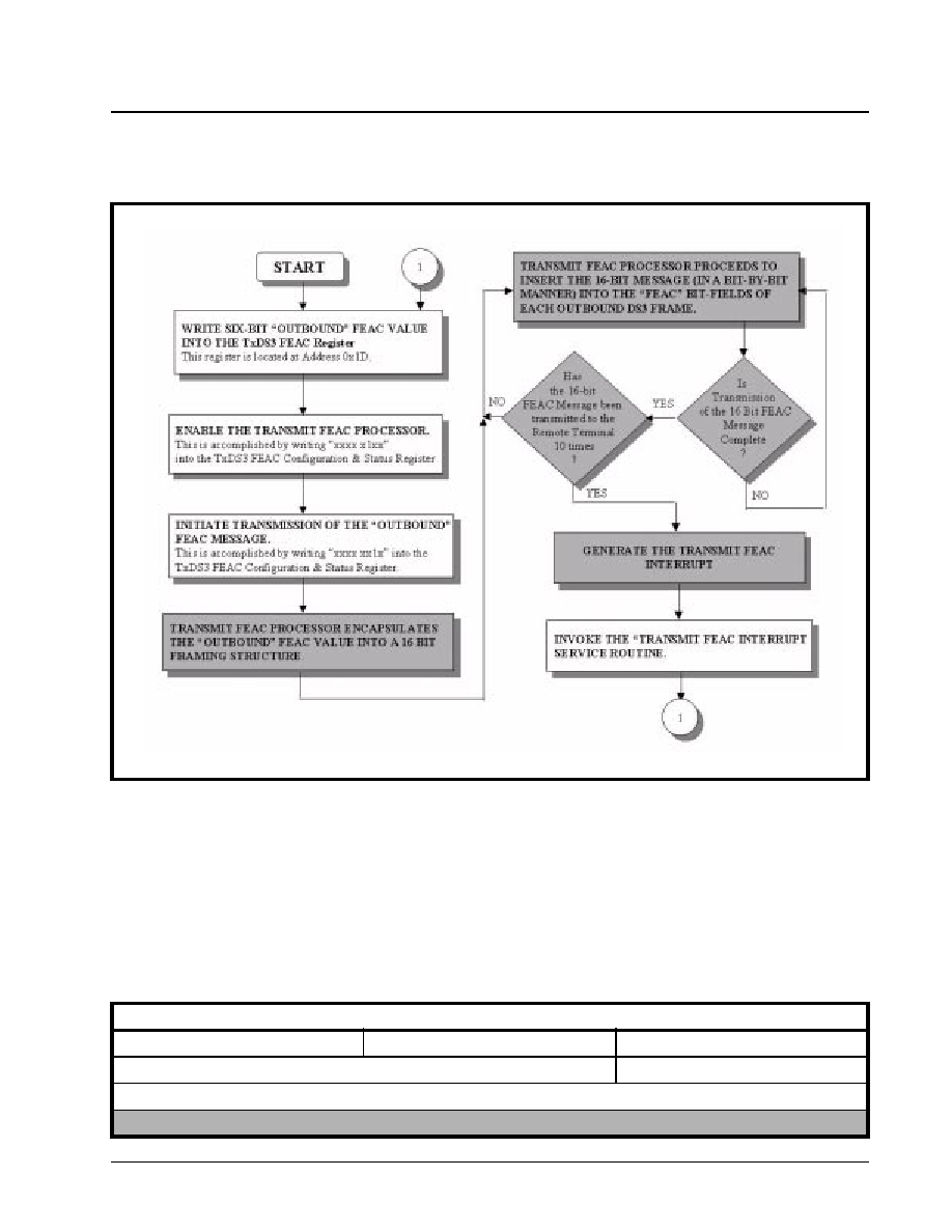
·Á
·Á
·Á
·Á
DS3 UNI FOR ATM
XRT7245
PRELIMINARY
REV. 1.03
195
Figure 51 presents a flow chart depicting how to use
the Transmit FEAC Processor.
For a detailed description of the Receive FEAC
Processor, please see Section 7.1.2.5.
6.4.4.1.3
The LAPD Transmitter
The LAPD Transmitter allows the user to transmit
path maintenance data link messages to the "Far-
End" Receive via the "outbound" DS3 Frames. In this
case the message bits are inserted into and carried
by the 3 "DL" bit fields of F-Frame #5 within each
DS3 M-frame. The on-chip LAPD transmitter sup-
ports both the 76 byte and 82 byte length message
formats, and the UNI allocates 88 bytes of on-chip
RAM (e.g., the "Transmit LAPD Message" buffer) to
store the message to be transmitted. The message
format complies with ITU-T Q.921 (LAPD) protocol
with different addresses and is presented below in Ta-
ble 31.
t
F
IGURE
51. A F
LOW
C
HART
DEPICTING
HOW
TO
TRANSMIT
A
FEAC M
ESSAGE
VIA
THE
FEAC T
RANSMITTER
T
ABLE
31: LAPD M
ESSAGE
F
RAME
F
ORMAT
F
LAG
S
EQUENCE
(8
BITS
)
SAPI (6-bits)
C/R
EA
TEI (7 bits)
EA
Control (8-bits)
76 or 82 Bytes of Information (Payload)
XRT7245
DS3 UNI FOR ATM
·Á
·Á
·Á
·Á
PRELIMINARY
REV. 1.03
196
Where: Flag Sequence = 7Eh
SAPI + CR + EA = 3Ch or 3Eh
TEI + EA = 01h
Control = 03h
The following section defines each of these bit/byte-
fields within the LAPD Message Frame Format.
Flag Sequence Byte
The Flag Sequence byte is of the value 7Eh, and is
used to denote the boundaries of the LAPD Message
Frame.
SAPI--Service Access Point Identifier
The SAPI bit-fields are assigned the value of
"001111b" or 15
10
.
TEI--Terminal Endpoint Identifier
The TEI bit-fields are assigned the value of 00h. The
TEI field is used in N-ISDN systems to identify a ter-
minal out of multiple possible terminal. However,
since the UNI transmits data in a point-to-point man-
ner, the TEI value is unimportant.
Control
The Control identifies the type of frame being trans-
mitted. There are three general types of frame formats:
Information, Supervisory, and Unnumbered. The UNI
assigned the Control byte the value 03h. Hence, the
UNI will be transmitting and receiving Unnumbered
LAPD Message frames.
Information Payload
The "Information Payload" is the 76 bytes or 82 bytes
of data (e.g., the PMDL Message) that the user has
written into the on-chip "Transmit LAPD Message"
buffer (which is located at addresses 86h through DDh).
It is important to note that the user must write in a
specific octet value into the first byte position within
the Transmit LAPD Message buffer (located at Ad-
dress = 86h, within the UNI). The value of this octet
depends upon the type of LAPD Message frame/PM-
DL Message that the user wishes to transmit. Table 31
presents a list of the various types of LAPD Message
frames/PMDL Messages that are supported by the
XRT7245 DS3 UNI device; and the corresponding
octet value that the user must write into the first octet
position within the "Transmit LAPD Message" buffer.
Frame Check Sequence Bytes
The 16 bit FCS (Frame Check Sequence) is calculated
over the LAPD Message Header and Information
Payload bytes, by using the CRC-16 polynomial, x
16
+ x
12
+ x
5
+ 1.
Operation of the LAPD Transmitter
If the user wishes to transmit a message via the LAPD
Transmitter, he/she must write the information portion
(or the body) of the message into the Transmit LAPD
Message Buffer, which is located at 86h through DDh
in on-chip RAM via the Microprocessor Interface.
Afterwards, the user must do three things:
1.
Specify the type of LAPD message to be
transmitted.
2.
Enable the LAPD Transmitter
3.
Initiate the Transmission
FCS--MSB
FCS--LSB
Flag Sequence (8-bits)
T
ABLE
31: LAPD M
ESSAGE
F
RAME
F
ORMAT
F
LAG
S
EQUENCE
(8
BITS
)
T
ABLE
32: T
HE
LAPD M
ESSAGE
T
YPE
AND
THE
C
ORRESPONDING
VALUE
OF
THE
F
IRST
B
YTE
,
WITHIN
THE
I
NFORMATION
P
AYLOAD
LAPD M
ESSAGE
T
YPE
V
ALUE
OF
F
IRST
B
YTE
,
WITHIN
I
NFORMATION
P
AYLOAD
OF
M
ESSAGE
M
ESSAGE
S
IZE
CL Path Identification
38h
76 bytes
IDLE Signal Identification
34h
76 bytes
Test Signal Identification
32h
76 bytes
ITU-T Path Identification
3Fh
82 bytes
·Á
·Á
·Á
·Á
DS3 UNI FOR ATM
XRT7245
PRELIMINARY
REV. 1.03
197
Each of these steps will be discussed in detail.
Specifying the Type of LAPD Message
The user can transmit one of four different types of
LAPD Messages. He/she can accomplish this by
writing the appropriate data to bits 1 and 2 of the Tx
DS3 LAPD Configuration Register. The bit-format of
this register is presented below.
The relationship between the contents of bit-fields 1
and 2 and the LAPD Message type follows.
Note: The Message Type selected must correspond with
the contents of the first byte of the Information (Payload)
portion, as presented in Table 33.
Enabling the LAPD Transmitter
Prior to the transmission of any data via the LAPD
Transmitter, the user must enable the LAPD
Transmitter. He/she can accomplish this by writing a
"1" to bit 0 of the Tx DS3 LAPD Configuration Register,
as depicted below.
Bit 0--TxLAPD Enable
This bit-field allows the user to enable or disable the
LAPD Transmitter in accordance with the following ta-
ble.
Transmit DS3 LAPD Configuration Register (Address = 1Eh)
B
IT
7
B
IT
6
B
IT
5
B
IT
4
B
IT
3
B
IT
2
B
IT
1
B
IT
0
Unused
Auto Retransmit
TxLAPD Type[1]
TxLAPD Type[0]
TxLAPD Enable
R/W
R/W
R/W
R/W
T
ABLE
33: R
ELATIONSHIP
BETWEEN
T
X
LAPDT
YPE
[1:0]
AND
THE
LAPD M
ESSAGE
T
YPE
/S
IZE
T
X
LAPD T
YPE
[1, 0]
LAPD M
ESSAGE
T
YPE
/S
IZE
00
LAPD Message type is "Test Signal" type. The size of this message is 76 bytes
01
LAPD Message type is "Idle Signal Identification" type. The size of this message is 76 bytes.
10
LAPD Message type is "CL Path Identification Type". The size of this message is 76 bytes
11
LAPD Message type is "ITU Path Identification Type". The size of this message is 82 bytes.
Transmit DS3 LAPD Configuration Register (Address = 1Eh)
B
IT
7
B
IT
6
B
IT
5
B
IT
4
B
IT
3
B
IT
2
B
IT
1
B
IT
0
Unused
Auto Retransmit
TxLAPD Type[1]
TxLAPD Type[0]
TxLAPD Enable
R/W
R/W
R/W
R/W
T
ABLE
34: T
HE
R
ELATIONSHIP
BETWEEN
THE
CONTENT
OF
THE
"T
X
LAPD E
NABLE
"
BIT
-
FIELD
AND
THE
ACTION
OF
THE
LAPD T
RANSMITTER
T
X
LAPD
E
NABLE
R
ESULTING
A
CTION
OF
THE
LAPD T
RANSMITTER
0
The LAPD Transmitter is disabled and the DL bits, in the DS3 frame, are transmitted as all "1"s.
1
The LAPD Transmitter is enabled and is transmitting a continuous stream of Flag Sequence octets (7Eh).
XRT7245
DS3 UNI FOR ATM
·Á
·Á
·Á
·Á
PRELIMINARY
REV. 1.03
198
Note: Upon power up or reset, the LAPD Transmitter is
disabled. Therefore, the user must set this bit to "1" in order
to enable the LAPD Transmitter.
Initiate the Transmission
At this point, the LAPD Transmitter is ready to begin
transmission. The user has written the "information
portion" of the message into the on-chip Transmit
LAPD buffer, specified the type of LAPD message
that he/she wishes to transmit, and has enabled the
LAPD Transmitter. The only thing remaining to do is
to initiate the transmission of this message. The user
initiates this process by writing a "1" to Bit 3 of the Tx
DS3 LAPD Status/Interrupt Register (TxDL Start).
The bit format of this register is presented below.
A "0" to "1" transition of Bit 3 (TxDL Start) in this reg-
ister, initiates the transmission of the data link mes-
sage. While the LAPD transmitter is transmitting the
message, the `TxDL Busy' (bit 2) bit will be set to "1".
This bit-field allows the user to "poll" the status of the
LAPD Transmitter. Once the message transfer is com-
pleted, this bit-field will toggle back to `0'.
The user can configure the LAPD Transmitter to inter-
rupt the local µC/µP upon completion of transmission
of the LAPD Message, by setting bit-field 1 (TxLAPD
Interrupt Enable) of the "Tx DS3 LAPD Status/Interrupt"
register to "1". The purpose of this interrupt is to let
the local µC/µP know that the LAPD Transmitter is
available and ready to transmit a new message. Bit 0
will reflect the status for the LAPD Transmitter interrupt.
Note: this bit-field will be reset on reading this register.
Once the user has invoked the "TxDL Start" com-
mand, the LAPD Transmitter will do the following.
∑
Generate the four octets of LAPD frame header
(e.g., Flag Sequence, SAPI, TEI, Control, etc.) and
insert it into the LAPD Message, prior to the user's
information (see the LAPD Message Frame Format
in Figure 52).
∑
Compute the 16 bit "Frame Check Sum" (FCS) of
the LAPD Message Frame (e.g., of the LAPD
Message header and information payload) and
append this value to the LAPD Message.
∑
Append a "trailer" Flag Sequence octet to the end
of the message LAPD (following the 16 bit FCS
value).
∑
Serialize the composite LAPD message and begin
inserting the LAPD message into the "DL" bit fields
of each outgoing DS3 Frame.
∑ Complete the transmission of the frame overhead,
payload, FCS value, and trailer Flag Sequence
octet via the Transmit DS3 Framer.
Once the LAPD Transmitter has completed its trans-
mission of the LAPD Message, the UNI will generate
an interrupt to the local µC/µP (if enabled). Afterwards,
the LAPD Transmitter will proceed to retransmit the
LAPD Message, repeatedly at one second intervals. In
between these transmissions of the LAPD Message,
the LAPD Transmitter will be sending a continuous
stream of "Flag Sequence Bytes". The LAPD Trans-
mitter will continue this behavior until the user has
disabled the LAPD Transmitter by writing a "0" to bit 0
(TxLAPD Enable) within the Tx DS3 LAPD Configu-
ration Register. If the LAPD Transmitter is inactive,
then it will continuously send the Flag Sequence
octets (via the "DL" bits of each outbound DS3
Frame) to the Far-End Receiver.
Note: In order to prevent the user's data (the payload por-
tion of the LAPD Message Frame) from mimicking the "Flag
Sequence" byte, the LAPD Transmitter will insert a "0" into
the LAPD data stream immediately following the detection
of five (5) consecutive "1s" (this "stuffing" occurs only while
the information payload is being transmitted). The `Far End'
LAPD Receiver (see Section 7.1.2.6) will have the respon-
sibility of detecting the 5 consecutive "1s" and removing the
subsequent "0" from the payload portion of the incoming
LAPD message.
Figure 52 presents a flow chart depicting the proce-
dure (in `white boxes') that the user should use in
order to transmit a LAPD message. This figure also
indicates (via the "shaded" boxes) what the LAPD
Transmitter circuitry will do before and during
message transmission.
Tx DS3 LAPD Status/Interrupt Register (Address = 1Fh)
B
IT
7
B
IT
6
B
IT
5
B
IT
4
B
IT
3
B
IT
2
B
IT
1
B
IT
0
Unused
Tx DL Start
Tx DL Busy
TxLAPD
Interrupt Enable
TxLAPD
Interrupt Status
R/W
R/O
R/W
RUR
·Á
·Á
·Á
·Á
DS3 UNI FOR ATM
XRT7245
PRELIMINARY
REV. 1.03
199
The Mechanics of Transmitting a New LAPD
Message
As mentioned above, after the LAPD Transmitter has
been enabled and commanded to transmit the mes-
sage residing in the "Transmit LAPD Message" buff-
er; it will continue to transmit this message at one-
second intervals. If the user wishes to transmit anoth-
er (e.g., different) PMDL message to the "Far End"
LAPD Receiver, he/she will have to write this "new"
message into the "Transmit LAPD Message" buffer,
via the Microprocessor Interface section of the UNI.
However, the user must be careful when writing in
this new message. If he/she writes this message into
the "Transmit LAPD Message" buffer at the "wrong
time" (with respect to these "one-second" transmis-
sions), the user's action could interfere with these
transmissions; thereby causing the LAPD Transmitter
to transmit a "corrupted" message to the "Far-End"
LAPD Receiver. In order to avoid this problem, while
writing the new message into the "Transmit LAPD
Message" buffer the user should do the following:
1.
Configure the UNI to automatically reset acti-
vated interrupts
The user can do this by writing a "1" into Bit 5 of the
UNI I/O Control Register, as depicted below.
This action will prevent the LAPD Transmitter from
generating its own "one-second" interrupts.
2.
Enable the "One-Second" Interrupt
F
IGURE
52. F
LOW
C
HART
DEPICT
HOW
TO
USE
THE
LAPD T
RANSMITTER
START
WRITE IN DATA LINK INFORMATION
The user accomplishes this by writing the
information that he/she wishes to transmit
(via the LAPD Transmitter) to locations 86h
through DDh, within the UNI Address Space.
ENABLE THE LAPD
TRANSMITTER FOR TRANSMISSION
This is accomplished by writing 00000xx1b
to the Tx DS3 LAPD Configuration Register
(where xx dictates LAPD Message Type).
INITIATE TRANSMISSION OF LAPD
MESSAGE
This is accomplished by writing 000010x0b
to the Tx DS3 LAPD Status/Interrupt
Register (where x indicates the user's choice
to enable/disable "LAPD Message Transfer
Complete" Interrupt).
LAPD Transmitter inserts Frame Header
octets in front of the user payload.
LAPD Transmitter computes the 16 bit FCS
(a CRC-16 value) and inserts it into the LAPD
Message, following the user payload
LAPD Transmitter appends a Flag Sequence
Trailer octet to the end of the LAPD Message
(after the 16 bit FCS).
Is
5 consecutive
"1s" detected
?
Is
Message
Transmission
Complete
?
Insert a "0" after the
string of 5 consecutive
"1s"
END
Generate Interrupt
LAPD Transmitter will
continue to transmit
Flag Sequence octets.
Yes
No
Yes
No
Address = 01h, UNI I/O Control Register
B
IT
7
B
IT
6
B
IT
5
B
IT
4
B
IT
3
B
IT
2
B
IT
1
B
IT
0
LOC Enable
Test PMON
IntEn Reset
AMI
Unipolar
TxClk Inv
RxClk Inv
Reframe
R/W
R/W
R/W
R/W
R/W
R/W
R/W
R/W
1
0
1
0
0
0
0
0
XRT7245
DS3 UNI FOR ATM
·Á
·Á
·Á
·Á
PRELIMINARY
REV. 1.03
200
This can be done by writing a "1" into Bit 0 of the UNI
Interrupt Enable Register, as depicted below.
3.
Write the new message into the "Transmit LAPD
Message" buffer immediately after the occur-
rence of the "One-Second" interrupt.
By timing the writes to the "Transmit LAPD Message"
buffer to occur immediately after the occurrence of
the "One-Second" interrupt, the user avoids conflict-
ing with the "one-second" transmissions of the LAPD
Message, and will transmit the correct messages to
the "Far-End" LAPD Receiver.
6.4.4.1.4
Manipulating the FEBE bit-fields of
the outbound DS3 Frames
The Transmit DS3 Framer allows the user to manipulate
the contents of the FEBE bit-fields in the outbound
DS3 frame. The user can accomplish this by writing
the appropriate data to the upper nibble of the Tx DS3
M-Bit Mask Register, as depicted below.
Each of these "FEBE-related" bit-fields are defined
below.
Bit 4--FEBE Register Enable
Writing a "1" to this "Read/Write" bit-field causes the
Transmit DS3 Framer to overwrite the internally
generated FEBE bits with the contents of the
TxFEBEDat[2:0] bit-fields (within this register) into
the outbound DS3 Frames.
Writing a "0" to this bit-field causes the Transmit DS3
Framer to transmit the internally generated FEBE bit-
values via the outbound DS3 Frames.
6.4.4.2
Programmable Pattern Generator
The Programmable Pattern Generator (PPG) allows
the user to override the Overhead Generator portion
of the Transmit DS3 Framer, in order to do the follow-
ing via software command:
∑
Generate Yellow Alarms
∑
Manipulate the X-bit (set them to "1")
∑
Generate the AIS Pattern
∑
Generate the IDLE pattern
∑
Generate the LOS pattern
∑ Generate FERF (Yellow) Alarms, in response to
various conditions.
In some cases, the user may wish to generate these
signals in response to an interrupt, or upon sensing
certain conditions. In other cases, the user may wish
to generate some of these signals for Equipment
Testing Purposes.
The user can exercise each of these options by writ-
ing the appropriate data to the Tx DS3 Configuration
Address = 04h, UNI Interrupt Enable Register
B
IT
7
B
IT
6
B
IT
5
B
IT
4
B
IT
3
B
IT
2
B
IT
1
B
IT
0
RxDS3
Interrupt
Enable
RxPLCP
Interrupt
Enable
RxCP
Interrupt
Enable
Rx UTOPIA
Interrupt
Enable
Tx UTOPIA
Interrupt
Enable
Tx CP
Interrupt
Enable
Tx DS3
Interrupt
Enable
One Sec
Interrupt
Enable
R/W
R/W
R/W
R/W
R/W
R/W
R/W
R/W
0
0
0
0
0
0
0
1
Tx DS3 M-Bit Mask Register, Address = 17h
B
IT
7
B
IT
6
B
IT
5
B
IT
4
B
IT
3
B
IT
2
B
IT
1
B
IT
0
TxFEBE
Dat[2]
TxFEBE
Dat[1]
TxFEBE
Dat[0]
FEBE
Reg Enable
TxErr PBit
MBit Mask(2) MBit Mask(1) MBit Mask(0)
R/W
R/W
R/W
R/W
R/W
R/W
R/W
R/W
·Á
·Á
·Á
·Á
DS3 UNI FOR ATM
XRT7245
PRELIMINARY
REV. 1.03
201
Register (Address = 16h). The bit format of this register
is presented below.
The role/function of each of these bit-fields within the
register, are discussed below.
6.4.4.2.1
Transmit Yellow Alarm--Bit 7
This "read/write" bit field allows the user to transmit a
Yellow Alarm to the "Far-End" Receive DS3 Framer
via software control. If the user opts to transmit a
"Yellow Alarm" then all of the X-bits, in the outbound
DS3 frames will be set to `0'. The following table re-
lates the content of this bit field to the Transmit DS3
Framer's action.
Note: This bit is ignored when either the "TxIDLE",
"TxAIS", or the "TxLOS" bit-fields are set.
6.4.4.2.2
Transmit X-bit--Bit 6
This bit field functions as the logical complement of
Bit 7. This "read/write" bit field allows the user to
force all of the X-bits, in the outgoing DS3 frame, to
"1" and transmit them to the "Far-End" Receiver. The
following table relates the content of this bit field to
the Transmit DS3 Framer's action.
Note: This bit is ignored when either the Transmit Yellow
Alarm, Tx AIS, Tx IDLE, or TxLOS bit is set.
6.4.4.2.3
Transmit Idle (Condition) Pattern--Bit 5
This "read/write" bit field allows the user to transmit an
"Idle Condition" pattern to the "Far-End" Receiver upon
software control. The following table relates the
contents of this bit field to the Transmit DS3 Framer's
action.
Tx DS3 Configuration Register (Address = 16h)
B
IT
7
B
IT
6
B
IT
5
B
IT
4
B
IT
3
B
IT
2
B
IT
1
B
IT
0
Tx
Yellow
Alarm
Tx X-Bit
Tx IDLE
Pattern
Tx AIS
Pattern
Tx LOS
Pattern
FERF on
LOS
FERF on
OOF
FERF on AIS
R/W
R/W
R/W
R/W
R/W
R/W
R/W
R/W
T
ABLE
35: T
HE
R
ELATIONSHIP
BETWEEN
THE
CONTENTS
OF
B
IT
7 (T
X
Y
ELLOW
A
LARM
)
WITHIN
THE
T
X
DS3
C
ONFIGURATION
R
EGISTER
,
AND
THE
RESULTING
T
RANSMIT
DS3 F
RAMER
A
CTION
B
IT
7
T
RANSMIT
DS3 F
RAMER
'
S
A
CTION
0
Normal Operation: The X-bits are generated by the UNI based upon "Near End" Receiving Conditions"
(via the Receive DS3 Framer of the UNI chip)
1
Transmit Yellow Alarm: The Transmit DS3 Framer will overwrite the X-bits by setting them all to "0". The
payload information is not modified and is transmitted as normal.
T
ABLE
36: T
HE
R
ELATIONSHIP
BETWEEN
THE
CONTENTS
OF
B
IT
6 (T
X
X-B
ITS
)
WITHIN
THE
T
X
DS3 C
ONFIGURATION
R
EGISTER
,
AND
THE
RESULTING
T
RANSMIT
DS3 F
RAMER
A
CTION
B
IT
6
T
RANSMIT
DS3 F
RAMER
'
S
A
CTION
0
Normal Operation: The X-bits are generated by the UNI based upon "Receiving Conditions" (via the Receive
Section of the UNI chip)
1
Set X-bits to "1". The Transmit DS3 Framer will overwrite the X-bits by setting them to "1". Payload informa-
tion is not modified and is transmitted as normal.

XRT7245
DS3 UNI FOR ATM
·Á
·Á
·Á
·Á
PRELIMINARY
REV. 1.03
202
Note: This bit is ignored when either the "Tx AIS" or the
"Tx LOS" bit is set.
6.4.4.2.4
Transmit AIS Pattern--Bit 4
This "read/write" bit field allows the user to transmit
an AIS pattern to the "Far End" Receiver, upon soft-
ware control. The following table relates the contents
of this bit field to the Transmit DS3 Framer's action.
Note: This bit is ignored when the TxLOS bit is set.
6.4.4.2.5
Transmit LOS Pattern--Bit 3
This "read/write" bit field allows the user to transmit
an LOS (Loss of Signal) pattern to the "Far-End"
Receiver, upon software control. The following table
relates the contents of this bit field to the Transmit
DS3 Framer's action.
Note: When this bit is set, it overrides all of the other bits in
this register.
T
ABLE
37: T
HE
R
ELATIONSHIP
BETWEEN
THE
CONTENTS
OF
B
IT
5 (T
X
I
DLE
)
WITHIN
THE
T
X
DS3 C
ONFIGURATION
R
EGISTER
,
AND
THE
RESULTING
T
RANSMIT
DS3 F
RAMER
A
CTION
B
IT
5
T
RANSMIT
DS3 F
RAMER
'
S
A
CTION
0
Normal Operation: The OH- and Payload-bits are generated and/or transmitted by the UNI based upon "Near
End Receive Conditions" (e.g., the Receive DS3 Framer of this UNI chip)
1
Transmit Idle Condition Pattern. When this command is invoked, the Transmit DS3 Framer will do the follow-
ing:
Set the X-bits to "1"
Set the CP-Bits (F-Frame #3) to "0"
Generate Valid M, F, and P bits
Overwrite the data in the DS3 payload with a repeating "1100..." pattern.
T
ABLE
38: T
HE
R
ELATIONSHIP
BETWEEN
THE
CONTENTS
OF
B
IT
4 (T
X
AIS P
ATTERN
)
WITHIN
THE
T
X
DS3
C
ONFIGURATION
R
EGISTER
,
AND
THE
RESULTING
T
RANSMIT
DS3 F
RAMER
A
CTION
B
IT
4
T
RANSMIT
DS3 F
RAMER
'
S
A
CTION
0
Normal Operation: The X-bits are generated by the UNI based upon "Receiving Conditions" (via the Receive
Section of the UNI chip)
1
Transmit AIS Pattern. When this command is invoked, the Transmit DS3 Framer will do the following.
∑ Set the X-bits to "1"
∑ Set all the C-bits to "0"
∑ Generate valid M, F, and P bits
∑ Overwrite the data in the DS3 payload with a repeating "1010..." pattern
T
ABLE
39: T
HE
R
ELATIONSHIP
BETWEEN
THE
CONTENTS
OF
B
IT
3 (T
X
LOS)
WITHIN
THE
T
X
DS3 C
ONFIGURATION
R
EGISTER
,
AND
THE
RESULTING
T
RANSMIT
DS3 F
RAMER
A
CTION
B
IT
3
T
RANSMIT
DS3 F
RAMER
'
S
A
CTION
0
Normal Operation: The OH- and Payload-bits are generated by the Transmit DS3 Framer based upon "Near
End" Receiving Conditions" (via the Receive Section of the UNI chip), and ATM Layer processor transmission
requirements.
1
Transmit LOS Pattern: When this command is invoked the Transmit DS3 Framer will do the following.
Set all OH bits to "0" (including the M, F, and P bits)
Overwrite the DS3 payload with an "all zero" pattern.

·Á
·Á
·Á
·Á
DS3 UNI FOR ATM
XRT7245
PRELIMINARY
REV. 1.03
203
6.4.4.2.6
FERF on LOS--Bit 2
This "Read/Write" bit-field allows the user to configure
the Transmit DS3 Framer to automatically generate a
"Yellow Alarm" if the Near-End Receive DS3 Framer
detects a "LOS" (Loss of Signal) Condition.
Writing a "1" to this bit-field enables this feature.
Writing a "0" to this bit-field disables this feature.
6.4.4.2.7
FERF on OOF--Bit 1
This "Read/Write" bit-field allows the user to configure
the Transmit DS3 Framer to automatically generate a
"Yellow Alarm" if the Near-End Receive DS3 Framer
detects an "OOF (Out-of-Frame) Condition".
Writing a "1" to this bit-field enables this feature.
Writing a "0" to this bit-field disables this feature.
6.4.4.2.8
FERF on AIS--Bit 0
This "Read/Write" bit-field allows the user to configure
the Transmit DS3 Framer to automatically generate a
"Yellow Alarm" if the Near-End Receive DS3 Framer
detects an AIS (Alarm Indication Signal) Condition.
Writing a "1" to this bit-field enables this feature.
Writing a "0" to this bit-field disables this feature.
6.4.4.3
Using the TxOH Serial Input Port
The TxOH Serial Input port allows the user to insert
his/her value(s) for the OH bits into the outbound
DS3 frames. The TxOH Serial Input port is activated
when the user asserts the TxOHIns pin (e.g., toggles
this input pin "high"). Once this serial port is activated,
then the user is expected to serially apply his/her
choices for the DS3 OH bits at the TxOH input pin.
The TxOHClk output pin functions as a clock that will
sample and latch the data at the TxOH input pin on
its rising edge. The frequency of this TxOHClk clock
signal is approximately 526 kHz. The TxOHFrame
output signal is provided to inform the user when the
value for the first X-bit, within the DS3 M-Frame, is
expected. The TxOH Serial Input port expects the
user to apply his/her value for OH bits in the order
as presented in Figure 48. Specifically, when the
TxOHFrame output pin pulses "high", the TxOH
Serial Input Port will be expecting the first "X"-bit (of
F-Frame #1). On the very next clock pulse (TxOHClk),
the TxOH Serial Input Port will be expecting the
user's value for the "F1" bit, and so on.
The TxOH Serial Input port also allows the user to
selectively externally insert his/her value for the DS3
OH data (e.g, allowing some of the OH bits to be
internally generated, while inserting his/her own values
for the remaining overhead bits). This can be accom-
plished by "keeping track" of the number of clock
pulses occurring since the last assertion of the TxO-
HFrame signal, and by asserting the TxOHIns, at the
time the TxOH serial input port would be expecting
the "OH bit(s) that are to be externally inserted". The
TxOHIns input should be negated for the remainder
of the "M-Frame" sampling period, so that these OH
bits will be internally generated.
Figure 53 presents a timing diagram that illustrates
the behavior of the TxOH serial interface signals dur-
ing user input of the DS3 OH bits.
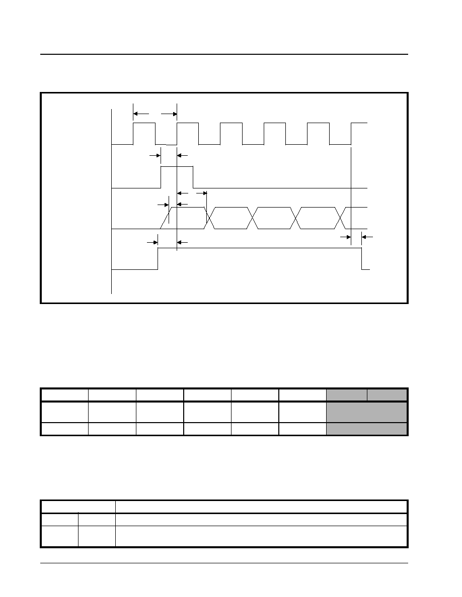
XRT7245
DS3 UNI FOR ATM
·Á
·Á
·Á
·Á
PRELIMINARY
REV. 1.03
204
6.4.4.4
Transmit DS3 Framer Timing
The Transmit DS3 Framer data may be generated
and clocked out of the UNI, based upon one of three
different timing or framing sources:
∑
Receive DS3 Framer timing
∑
TxInClk input signal
∑ TxFrameRef input signal
The user makes this selection by writing to Bits 0 and 1
of the UNI Operating Mode Register (Address = 00h);
as depicted below.
The following table lists the values of Bits 0 and 1 and
the resulting timing source for the Transmit DS3 Framer
block
F
IGURE
53. T
IMING
D
IAGRAM
ILLUSTRATING
THE
B
EHAVIOR
OF
THE
DS3 OH B
IT
S
ERIAL
I
NTERFACE
,
DURING
USER
INPUT
OF
OH B
ITS
.
TxOHFrame
TxOH
TxOHIns
TxOHClk
t25
t26
t27
t29
t28
t24
UNI Operating Mode Register: Address = 00h
B
IT
7
B
IT
6
B
IT
5
B
IT
4
B
IT
3
B
IT
2
B
IT
1
B
IT
0
Local
Loopback
Cell
Loopback
PLCP
Loopback
Reset
Direct
Mapped ATM
C-Bit/M13
TimRefSel[1, 0]
R/W
R/W
R/W
R/W
R/W
R/W
R/W
T
ABLE
40: T
HE
R
ELATIONSHIP
BETWEEN
T
IM
R
EF
S
EL
[1:0] (
E
.
G
., B
ITS
1
AND
0
OF
THE
UNI O
PERATION
M
ODE
R
EGISTER
),
AND
THE
RESULTING
T
IMING
/F
RAMING
S
OURCE
FOR
THE
T
RANSMIT
DS3 F
RAMER
BLOCK
T
IM
R
EF
S
EL
[1:0]
T
RANSMIT
DS3 F
RAMER
T
IMING
/F
RAME
S
OURCE
0
0
RxLineClk input signal--The Recovered Clock Signal from the incoming (received) DS3 line signal
0
1
1
1
TxInClk input signal. Framing is asynchronous on "power on".

·Á
·Á
·Á
·Á
DS3 UNI FOR ATM
XRT7245
PRELIMINARY
REV. 1.03
205
Each of these "potential" timing sources for the Transmit
DS3 Framer are discussed in greater detail below.
6.4.4.4.1
RxLineClk--Receive DS3 Framer
Timing
In this mode, the Transmit DS3 Framer timing is
based upon the recovered clock input signal,
RxLineClk, obtained by the Receive DS3 Framer.
This mode is convenient from the stand-point that it
requires no external timing source (to either the
TxFrameRef or TxInClk pins). However, this configu-
ration has one drawback: If the Receive DS3 Framer
block experiences an LOS condition, or somehow
loses the recovered clock signal, then the Transmit
DS3 Framer block essentially has no timing source.
Therefore, in this configuration, the operation of the
Transmit DS3 Framer block is dependent upon the
actions of the "Near-End" Receive DS3 Framer block
and its incoming DS3 data-stream signal.
6.4.4.4.2
TxInClk Input Signal
In this mode, the Transmit DS3 Framer block will use
the clock signal that is input at the TxInClk pin, as the
timing reference. If the user selects this mode, then
he/she must insure that a high quality 44.736 MHz
clock signal is applied at this input.
The advantage of using this timing signal as the
reference for the Transmit DS3 Framer, over the
RxLineClk signal is that an LOS condition (or a loss
of clock recovery event with the incoming DS3 line
signal) does not adversely affect the Transmit DS3
Framer's operation.
6.4.4.4.3
TxFrameRef Input Signal
In this mode, the Transmit DS3 Framer block will use
the input signal at the TxFrameRef input pin as the
"framing reference". In other words, a rising edge at
this input will cause the Transmit DS3 Framer to begin
its creation of a new DS3 M-frame. Consequently, the
user must supply a clock signal that is equivalent to
the DS3 frame rate (or 9398.3 Hz).
Note: The user is advised that these bit fields (within the
UNI Operating Mode Register) also affect the behavior of
the Transmit PLCP Processor. For more information on
how TimRefSel[1, 0] affects the Transmit PLCP Processor,
see Section 6.3.3.1.
6.4.4.5
Interfacing the Transmit DS3 Framer
to the Line
The XRT7245 DS3 ATM UNI is a digital device that
takes ATM cell data from an ATM Layer processor,
processes this cell data and ultimately maps this
information into the payload portion of an outbound
DS3 frame. However, the XRT7245 DS3 ATM UNI
lacks the current drive capability to be able to directly
transmit this DS3 data stream through some trans-
former-coupled coax cable with enough signal
strength for it to be received by the far-end receiver.
Therefore, in order to get around this problem, the
UNI requires the use of an LIU (Line Interface Unit) IC.
An LIU is a device that has sufficient drive capability,
along with the necessary pulse-shaping circuitry to
be able to transmit a signal through the transmission
medium in a manner that it can be reliably received
by the far-end receiver. Figure 55 presents a circuit
drawing depicting the UNI interfacing to an LIU
(XRT7296 DS3 Transmit LIU).
The Transmit DS3 Framer can transmit data to the
LIU IC or other external circuitry via two different out-
put modes: Unipolar or Bipolar. If the user selects
Unipolar (or Single Rail) mode, then the contents of
the DS3 Frame is output via the TxPOS pin to external
circuitry. The TxNEG pin will only be used to denote
the frame boundaries. TxNEG will pulse "high" for
one bit period, at the start of each new DS3 frame,
and will remain "low" for the remainder of the frame.
Figure 54 presents an illustration of the TxPOS and
TxNEG signals during data transmission while in the
Unipolar mode. This mode is sometimes referred to
as "Single Rail" mode because the data pulses only
exist in one polarity: positive.
1
0
TxFrameRef input signal.
T
ABLE
40: T
HE
R
ELATIONSHIP
BETWEEN
T
IM
R
EF
S
EL
[1:0] (
E
.
G
., B
ITS
1
AND
0
OF
THE
UNI O
PERATION
M
ODE
R
EGISTER
),
AND
THE
RESULTING
T
IMING
/F
RAMING
S
OURCE
FOR
THE
T
RANSMIT
DS3 F
RAMER
BLOCK
T
IM
R
EF
S
EL
[1:0]
T
RANSMIT
DS3 F
RAMER
T
IMING
/F
RAME
S
OURCE
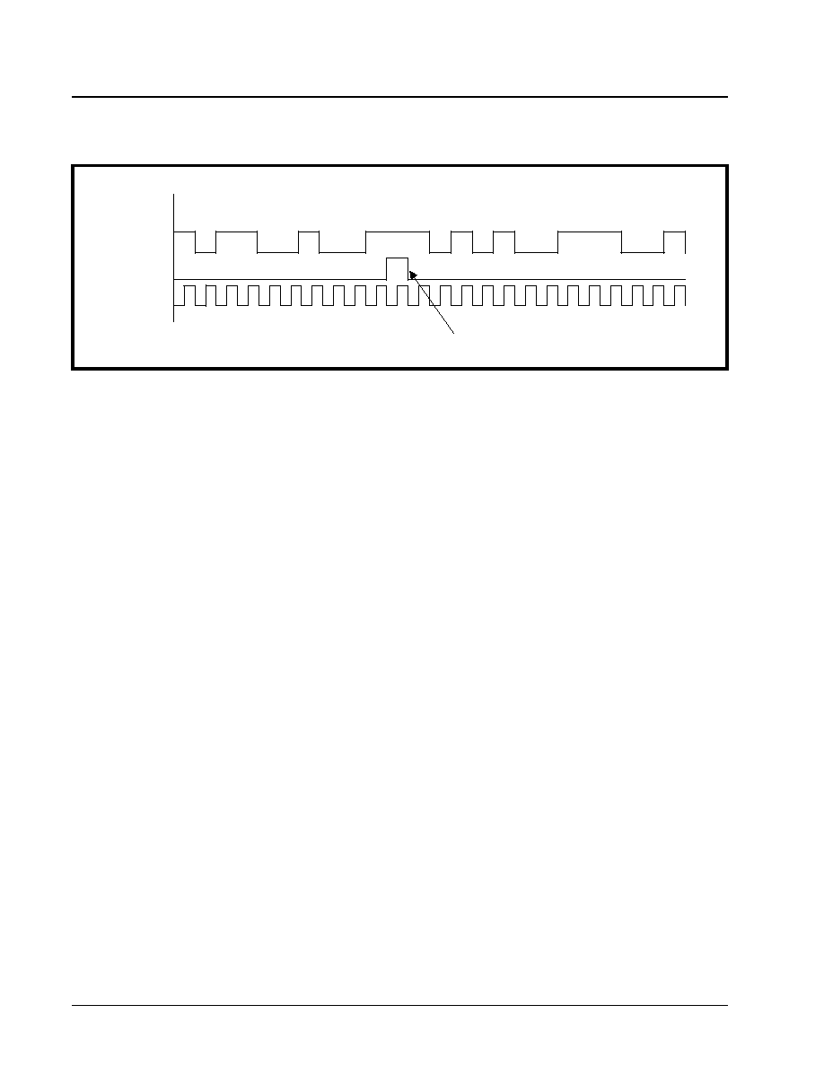
XRT7245
DS3 UNI FOR ATM
·Á
·Á
·Á
·Á
PRELIMINARY
REV. 1.03
206
Note: The user is advised not to transmit data via the
Unipolar mode, if he/she wishes to transmit this data to a
Far-End DS3 Terminal over some transformer-couple
medium. The user should, instead, use one of the Bipolar
mode line codes for this application. The Unipolar mode
can be used to drive signals through optical fiber. In this
case, the TxPOS output would be applied to an LED at the
electrical/optical interface circuitry.
When the UNI is operating in the Bipolar (or Dual
Rail) mode, then the contents of the DS3 Frame is
output via both the TxPOS and TxNEG pins. If the
user chooses the Bipolar mode, then he/she can
transmit the DS3 data to the Far-End Receiver via
one of two different line codes: Alternate Mark Inver-
sion (AMI) or Binary≠3 Zero Substitution (B3ZS).
Each one of these line codes will be discussed below.
Bipolar mode is sometimes referred to as "Dual Rail"
because the data pulses occur in two polarities-
TxNEG and TxLineClk output pins, for this mode are
discussed below.
F
IGURE
54. T
HE
B
EHAVIOR
OF
T
X
POS
AND
T
X
NEG
SIGNALS
DURING
DATA
TRANSMISSION
WHILE
THE
UNI
IS
OPERATING
IN
THE
U
NIPOLAR
M
ODE
TxPOS
TxNEG
TxLineClk
Data
Frame Boundary
1
0
1
1
0
0
1
0
0
1
1
1
0
1
0
1
0
0
1
1
1
0
0
1
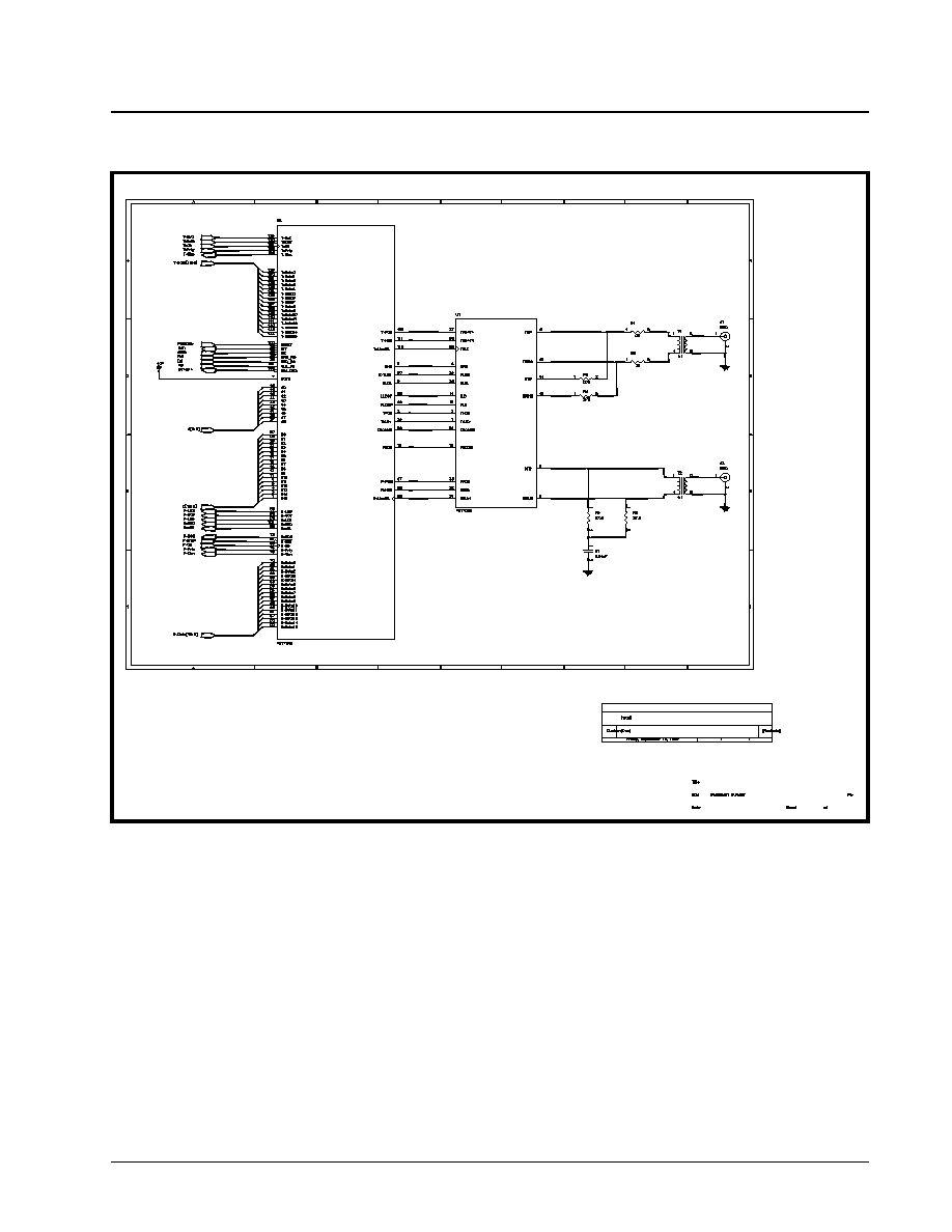
·Á
·Á
·Á
·Á
DS3 UNI FOR ATM
XRT7245
PRELIMINARY
REV. 1.03
207
TxPOS--Transmit Positive Polarity Pulse:
The UNI will
assert this output to the LIU IC when it desires for the
LIU to generate and transmit a "positive polarity" pulse
to the far-end receiver.
TxNEG--Transmit Negative Polarity Pulse:
The UNI will
assert this output to the LIU IC when it desires for the
LIU to generate and transmit a "negative polarity"
pulse to the far-end receiver.
TxLineClk--Transmit Line Clock:
The LIU IC uses this
signal from the UNI to sample the state of its TxPOS
and TxNEG inputs. The results of this sampling dic-
tates the type of pulse (positive polarity, zero, or neg-
ative polarity) that it will generate and transmit to the
far-end Receive DS3 Framer.
6.4.3.5.1 Line Codes
The user can select either Unipolar Mode or Bipolar
Mode by writing the appropriate value to Bit 3 of the
UNI I/O Control Register (Address = 01h), as shown
below.
F
IGURE
55. A
PPROACH
TO
I
NTERFACING
THE
XRT7245 UNI
DEVICE
TO
THE
XRT7300 DS3/E3/STS-1 LIU IC.
XRT7245
DS3 UNI FOR ATM
·Á
·Á
·Á
·Á
PRELIMINARY
REV. 1.03
208
The following table relates the value of this bit field to
the Transmit DS3 Framer I/O Mode.
Note:
1.
The default condition is the Bipolar Mode.
2.
This selection also affects the operation of the
Receive DS3 Framer block
6.4.4.5.0.1
Unipolar Mode Line Code
Please see Section 6.4.3.5
6.4.4.5.0.2
Bipolar Mode Line Codes
If the user chooses to operate the UNI in the Bipolar
Mode, then he/she can choose to transmit the DS3
data-stream via the AMI (Alternate Mark Inversion) or
the B3ZS Line Codes. The definition of AMI and
B3ZS line codes follow.
6.4.4.5.0.2.1
The AMI Line Code
AMI or Alternate Mark Inversion, means that consec-
utive "one's" pulses (or marks) will be of opposite
polarity with respect to each other. The line code
involves the use of three different amplitude levels:
+1, 0, and -1. +1 and -1 amplitude signals are used
to represent one's (or mark) pulses and the "0" ampli-
tude pulses (or the absence of a pulse) are used to
represent zeros (or space) pulses. The general rule
for AMI is: if a given "mark" pulse is of positive polarity,
then the very next "mark" pulse will be of negative
polarity and vice versa. This alternating-polarity rela-
tionship exists between two consecutive mark pulses,
independent of the number of `zeros' that may exist
between these two pulses. Figure 56 presents an
illustration of the AMI Line Code as would appear at
the TxPOS and TxNEG pins of the UNI, as well as
the output signal on the line.
UNI I/O Control Register (Address = 01h)
B
IT
7
B
IT
6
B
IT
5
B
IT
4
B
IT
3
B
IT
2
B
IT
1
B
IT
0
LOC Enable
Test Mode
Interrupt
Enable
Reset
AMI/B 325*
Unipolar/
Bipolar
TxCLK Inv
RxCLK Inv
Reframe
R/W
R/W
R/W
R/W
R/W
R/W
R/W
R/W
T
ABLE
41: T
HE
R
ELATIONSHIP
BETWEEN
THE
CONTENT
OF
B
IT
3 (U
NIPOLAR
/B
IPOLAR
*)
WITHIN
THE
UNI I/O
C
ONTROL
R
EGISTER
AND
THE
T
RANSMIT
DS3 F
RAMER
L
INE
I
NTERFACE
O
UTPUT
M
ODE
B
IT
3
T
RANSMIT
DS3 F
RAMER
L
INE
I
NTERFACE
O
UTPUT
M
ODE
0
Bipolar Mode: AMI or B3ZS Line Codes are Transmitted and Received
1
Unipolar (Single Rail) mode of transmission and reception of DS3 data is selected.
F
IGURE
56. I
LLUSTRATION
OF
AMI L
INE
C
ODE
Data
TxPOS
TxNEG
Line Signal
1 0
1 1
0 0
0
1
0
1 1
1
0
1
0 1
0
0 1
1 0 0
1
1
1
0
0
1
·Á
·Á
·Á
·Á
DS3 UNI FOR ATM
XRT7245
PRELIMINARY
REV. 1.03
209
Note: one of the main reasons that the AMI Line Code has
been chosen for driving transformer-coupled media is that
this line code introduces no dc component; thereby mini-
mizing dc distortion in the line.
6.4.4.5.0.2.2
The B3ZS Line Code
The Transmit DS3 Framer and the associated LIU IC
combine the data and timing information (originating
from the TxLineClk signal) into the line signal that is
transmitted to the far-end receiver. The far-end receiver
has the task of recovering this data and timing infor-
mation from the incoming DS3 data stream. Many
clock and data recovery schemes rely on the use of
Phase Locked Loop technology. Phase-Locked-Loop
(PLL) technology for clock recovery relies on transi-
tions in the line signal, in order to maintain "lock" with
the incoming DS3 data stream. However, PLL-based
clock recovery scheme, are vulnerable to the occur-
rence of a long stream of consecutive zeros (e.g., the
absence of transitions). This scenario can cause the
PLL to lose "lock" with the incoming DS3 data, there-
by causing the "clock" and data recovery process of
the receiver to fail. Therefore, some approach is
needed to insure that such a long string of consecu-
tive zeros can never happen. One such technique is
B3ZS encoding. B3ZS (or Bipolar 3 Zero Substitution)
is a form of AMI line coding that implements the
following rule.
In general the B3ZS line code behaves just like AMI;
with the exception of the case when a long string of
consecutive zeros occur on the line. Any string of 3
consecutive zeros will be replaced with either a "00V"
or a "B0V" where "B" refers to a Bipolar pulse (e.g., a
pulse with a polarity that is compliant with the AMI
coding rule). And "V" refers to a Bipolar Violation pulse
(e.g., a pulse with a polarity that violates the alternat-
ing polarity scheme of AMI.) The decision between
inserting an "00V" or a "B0V" is made to insure that
an odd number of Bipolar (B) pulses exist between any
two Bipolar Violation (V) pulses. Figure 57 presents a
timing diagram that illustrates examples of B3ZS en-
coding.
The user chooses between AMI or B3ZS line coding by
writing to bit 4 of the UNI I/O Control Register (Address =
01h), as shown below.
The following table relates the content of this bit-field
to the Bipolar Line Code that DS3 Data will be trans-
mitted and received at.
F
IGURE
57. I
LLUSTRATION
OF
TWO
EXAMPLES
OF
B3ZS E
NCODING
Data
TxPOS
TxNEG
0 0 V
Line Signal
B 0 V
1 0
1 1
0 0
0
1
0
1 1
1
0
1
0 1
0
0 1
1 1 0
1
1
1
0
0
1
UNI I/O Control Register (Address = 01h)
B
IT
7
B
IT
6
B
IT
5
B
IT
4
B
IT
3
B
IT
2
B
IT
1
B
IT
0
LOC
Enable Test
PMON
Interrupt
Enable
Reset
AMI/B3ZS*
Unipolar/
Bipolar*
TxClk Inv
RxClk Inv
Reframe
R/W
R/W
R/W
R/W
R/W
R/W
R/W
R/W
XRT7245
DS3 UNI FOR ATM
·Á
·Á
·Á
·Á
PRELIMINARY
REV. 1.03
210
Note:
1. This bit is ignored if Unipolar mode is selected.
2. This selection also affects the operation of the
Receive DS3 Framer block
6.4.4.5.1
TxLineClk Clock Edge Selection
The UNI also allows the user to specify whether the
DS3 output data (via TxPOS and/or TxNEG output
pins) is to be updated on the rising or falling edges of
the TxLineClk signal. This selection is made by writing
to bit 2 of the UNI I/O Control Register, as depicted
below.
The following table relates the contents of this bit field
to the clock edge of TxClk that DS3 Data is output on
the TxPOS and/or TxNEG output pins.
Note: The user will typically make the selection based
upon the "set-up" and "hold" time requirements of the
"Transmit LIU" IC.
Figure 59, Waveform/Timing Relationship between
TxLineClk, TxPOS and TxNEG-TxPOS and TxNEG
are configured to be updated on the rising edge of
TxLineClk.
T
ABLE
42: T
HE
R
ELATIONSHIP
BETWEEN
B
IT
4 (AMI/B3ZS*)
WITHIN
THE
UNI I/O C
ONTROL
R
EGISTER
AND
THE
B
IPOLAR
L
INE
C
ODE
THAT
IS
OUTPUT
BY
THE
T
RANSMIT
DS3 F
RAMER
B
IT
4
B
IPOLAR
L
INE
C
ODE
0
B3ZS
1
AMI
UNI I/O Control Register (Address = 01h)
B
IT
7
B
IT
6
B
IT
5
B
IT
4
B
IT
3
B
IT
2
B
IT
1
B
IT
0
LOC Enable
Test PMON
Interrupt
Enable
Reset
AMI/B3ZS*
Unipolar/
Bipolar*
TxLine Clk
Inv
RxLine Clk Inv
Reframe
R/W
R/W
R/W
R/W
R/W
R/W
R/W
R/W
T
ABLE
43: T
HE
R
ELATIONSHIP
BETWEEN
THE
CONTENTS
OF
B
IT
2 (T
X
L
INE
C
LK
I
NV
)
WITHIN
THE
UNI I/O C
ONTROL
R
EGISTER
AND
THE
T
X
L
INE
C
LK
CLOCK
EDGE
THAT
T
X
POS
AND
T
X
NEG
ARE
UPDATED
ON
B
IT
2
R
ESULT
0
Rising Edge: Outputs on TxPOS and/or TxNEG are updated on the rising edge of TxLineClk.
See Figure 50 for timing relationship between TxLineClk, TxPOS and TxNEG signals, for this selection.
1
Falling Edge: Outputs on TxPOS and/or TxNEG are updated on the falling edge of TxLineClk.
See
Figure 51 for timing relationship between TxLineClk, TxPOS and TxNEG signals, for this
selection.
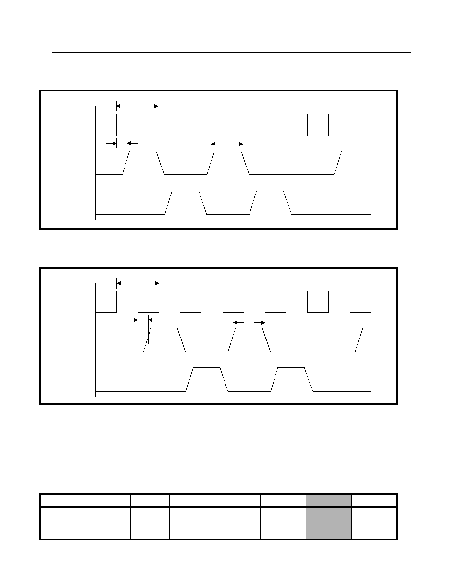
·Á
·Á
·Á
·Á
DS3 UNI FOR ATM
XRT7245
PRELIMINARY
REV. 1.03
211
6.4.4.6
Transmit DS3 Framer Interrupt
Processing
The Transmit DS3 Framer block will generate inter-
rupts upon the following conditions.
∑
Completion of Transmission of FEAC Message
∑ Completion of Transmission of LAPD Message
If one of these conditions occur, and if that particular
condition is enabled for interrupt generation, then
when the local
µ
P/
µ
C reads the UNI Interrupt Status
Register (during the early stages of Interrupt Process-
ing), as shown below; it should read xxxxxx1xb (where
the -b suffix denotes a binary expression, and the "x"
denotes a "don't care" value).
F
IGURE
58. W
AVEFORM
/T
IMING
R
ELATIONSHIP
BETWEEN
T
X
L
INE
C
LK
, T
X
POS
AND
T
X
NEG--T
X
POS
AND
T
X
NEG
ARE
CONFIGURED
TO
BE
UPDATED
ON
THE
FALLING
EDGE
OF
T
X
L
INE
C
LK
.
TxLineClk
TxPOS
TxNEG
t32
t30
t33
F
IGURE
59. W
AVEFORM
/T
IMING
R
ELATIONSHIP
BETWEEN
T
X
L
INE
C
LK
, T
X
POS
AND
T
X
NEG--T
X
POS
AND
T
X
NEG
ARE
CONFIGURED
TO
BE
UPDATED
ON
THE
FALLING
EDGE
OF
T
X
L
INE
C
LK
.
TxLineClk
TxPOS
TxNEG
t31
t32
t33
UNI Interrupt Status Register (Address = 05h)
B
IT
7
B
IT
6
B
IT
5
B
IT
4
B
IT
3
B
IT
2
B
IT
1
B
IT
0
RxDS3
IntStat
RxPLCP
IntStat
RxCP
IntStat
RxUTOPIA
IntStat
TxUTOPIA
IntStat
TxCP
IntStat
TxDS3
IntStat
OneSec
IntStat
RO
RO
RO
RO
RO
RO
RO
RO
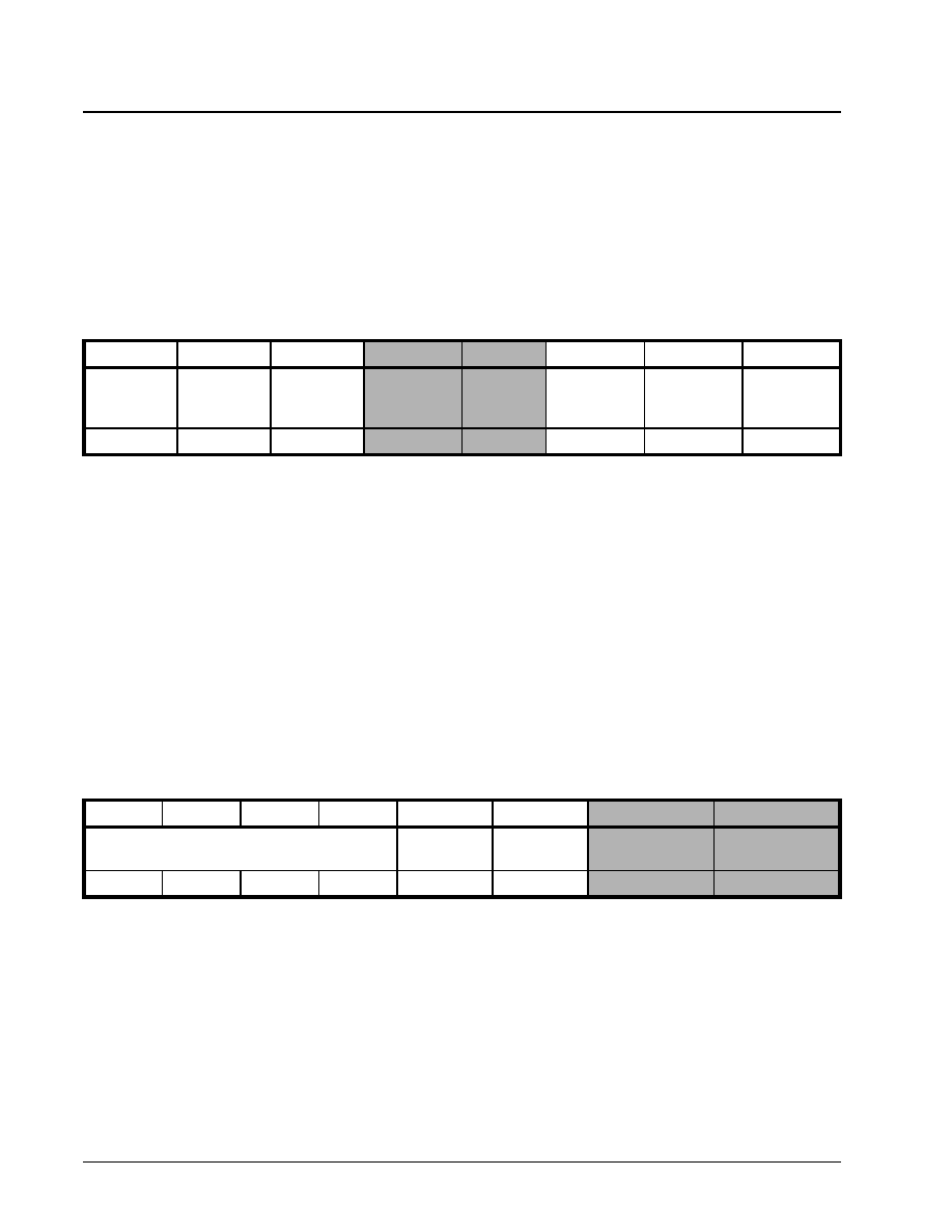
XRT7245
DS3 UNI FOR ATM
·Á
·Á
·Á
·Á
PRELIMINARY
REV. 1.03
212
At this point, the local µC/µP has determined that the
Transmit DS3 Framer block is the source of the inter-
rupt, and that the Interrupt Service Routine should
branch accordingly. In order to accomplish this, the local
µP/µC should now read one or both of the following
registers
∑
Tx DS3 FEAC Configuration and Status Register
(Address = 1Ch)
∑ Tx DS3 LAPD Status/Interrupt Register (Address =
1Fh)
The roles/functions of the bit-fields, within each of these
registers, relevant to interrupt processing, are described
below.
Tx DS3 FEAC Configuration and Status Register
The bit format of this register is presented below.
This register has five (5) active bit-fields. However,
only two of these bit-fields are relevant to interrupt
processing. Bit 3 is an Interrupt Status bit and Bit 4 is
an Interrupt Enable bit.
Bit 3--Tx FEAC Interrupt Status
This "Read-Only" bit-field is asserted once the Transmit
FEAC processor has completed its 10th transmission
of a FEAC message to the far-end receiver. Addition-
ally, the UNI will notify the local µC/µP of this fact by
asserting the INT* pin to the local µC/µP. The purpose
of this interrupt is to alert the local µC/µP that the
Transmit FEAC Processor has completed the trans-
mission of a FEAC message, and that it is now avail-
able and ready to transmit another FEAC message.
Bit 4--Tx FEAC Interrupt Enable
This "Read/Write" bit field allows the user to enable/
disable interrupts generated due to the Transmit FEAC
Processor completing its transmission of a FEAC mes-
sage to the "far end" receiver. The user can enable this
interrupt by writing a "1" to this bit. Upon power up or
reset conditions, this bit-field will contain a "0". There-
fore, the default condition is for this interrupt to be
disabled. The user must write a "1" to this bit-field in
order to enable this interrupt.
Tx DS3 LAPD Status/Interrupt Register
The bit format of this register is presented below.
This register has four (4) active bit fields. However,
only two of these bit-fields are relevant to interrupt
processing. Bit 0 is an interrupt status bit and Bit 1 is
an interrupt enable bit.
Bit-0--TxLAPD Interrupt Status
This "Reset-Upon-Read" bit field is asserted once
the DS3 LAPD Transmitter has completed transmis-
sion of a LAPD message to the "far-end" receiver. Addi-
tionally, the UNI will notify the local µC/µP of this fact
by asserting the INT* pin to the local µC/µP. The pur-
pose of this interrupt is to alert the local µC/µP that
the LAPD Transmitter has completed the transmission
of a LAPD message, and that it is ready and available
to transmit another LAPD message.
Bit-1--TxLAPD Interrupt Enable
This Read/Write bit field allows the user to enable/
disable interrupts generated due to the completion of
transmitting a LAPD message to the far end receiver.
The user can enable this interrupt by writing a "1" to
this bit. Upon power up or reset conditions, this bit-
field will contain a "0". Therefore, the default condition
Tx DS3 FEAC Configuration and Status Register (Address = 1Ch)
B
IT
7
B
IT
6
B
IT
5
B
IT
4
B
IT
3
B
IT
2
B
IT
1
B
IT
0
Not Used
Not Used
Not Used
Tx FEAC
Interrupt
Enable
Tx FEAC
Interrupt
Status
Tx FEAC
Enable
Tx FEAC Go
Tx FEAC
Busy
R/O
R/O
R/O
R/W
R/O
R/W
R/W
R/O
Tx DS3 LAPD Status/Interrupt Register (Address = 1Fh)
B
IT
7
B
IT
6
B
IT
5
B
IT
4
B
IT
3
B
IT
2
B
IT
1
B
IT
0
Unused
Tx DL Start
Tx DL Busy
TxLAPD Interrupt
Enable
TxLAPD Interrupt
Status
R/W
R/O
R/W
RUR

·Á
·Á
·Á
·Á
DS3 UNI FOR ATM
XRT7245
PRELIMINARY
REV. 1.03
213
is for this interrupt to be disabled. The user must
write a "1" to this bit in order to enable this interrupt.

XRT7245
DS3 UNI FOR ATM
·Á
·Á
·Á
·Á
PRELIMINARY
REV. 1.03
214
7.0 THE RECEIVE SECTION
The purpose of the Receiver Section of the XRT7245
DS3 ATM UNI device is to allow a local ATM Layer (or
ATM Adaptation Layer) processor to receive ATM cell
data from a remote piece of equipment via a public or
leased DS3 transport medium.
The Receive Section of the DS3 UNI chip consists of
the following functional blocks:
∑
Receive DS3 Framer
∑
Receive PLCP Processor
∑
Receive Cell Processor
∑ Receive UTOPIA Interface
The Receive DS3 Framer will synchronize itself to
this incoming DS3 Data Stream (containing ATM
cells) via the RxPOS, RxNEG, and RxLineClk input
pins, and proceed to "strip off" and process the OH
bits of the DS3 frame. Once all of the OH bits have
been removed, the payload portion of the received
DS3 Frame should consist of either PLCP frames or
ATM cells (if the Direct-Mapped ATM option was se-
lected). The PLCP frames are routed to the Receive
PLCP Processor and the "Direct-Mapped" ATM Cells
are sent onto the Receive Cell Processor.
The Receive PLCP Processor will take the PLCP
frame data and search for the A1/A2 Frame Align-
ment pattern bytes, in order to determine the PLCP
frame boundaries. Once PLCP framing is estab-
lished, the Receive PLCP Processor will proceed to
check and process the OH bytes, within the PLCP
frame. The PLCP Frames, along with framing infor-
mation are sent on to the Receive Cell Processor.
The Receive Cell Processor takes delineated PLCP
frames from the Receive PLCP Processor, and per-
forms the following operations:
∑
Performs Cell Delineation.
∑
HEC Byte Verification
It takes the first four octets of the cell (the header)
and computes a HEC byte. The Receive Cell Proces-
sor will then compare this computed HEC value with
that of the fifth octet, within the cell. If the two HEC
values are equal, the cell is then retained for further
processing. If the two HEC values are not equal, then
the cells with single-bit errors are corrected. Howev-
er, the cell is optionally discarded if multile-bit errors
are detected.
∑
Idle Cell Filtering
The Receive Cell Processor will detect and remove
Idle Cells and can be configured to filter User and
OAM cells.
∑ The Receive Cell Processor will de-scramble the
payload portion of the cell (the 6th through the 53rd
octet), and pack these octets in with the cell header
bytes, and the HEC byte for transmission to the
Receive UTOPIA block.
The following sections discuss the blocks comprising
the Receiver portion of the DS3 UNI in detail.
7.1
Receive DS3 Framer
7.1.1
Brief Description of the Receive DS3
Framer
The Receive DS3 Framer synchronizes itself to the
incoming DS3 data-stream. It decodes and frames
the incoming data into DS3 frames. It supports both
the M13 and C-bit Parity framing formats. It detects
Line Code Violations (LCV), the Loss of Signal (LOS)
condition, the Alarm Indication Signal (AIS) and Idle
patterns, Out of Frame (OOF) and Loss of Frame
(LOF) conditions. The Receive DS3 Framer computes
parity over a given DS3 M-frame and compares it
with the P-bits that it receives in the very next DS3
M`-hframe. It extracts and processes the DS3 frame
overhead bits and provides them to a serial output
port. It "validates" FEAC messages received from the
"Far-End" Transmit DS3 Framer. Additionally, the
Receive DS3 Framer will receive "LAPD Messages"
from the "Far End" Transmit DS3 Framer; and will
write this message into the "Receive LAPD Message"
buffer.
The Receive DS3 Framer will detect and generate
interrupts upon error conditions. The status of the
Receive DS3 Framer can be read by registers
through the UNI-Microprocessor interface. If the UNI
is operating in the "Direct-Mapped" ATM Mode, then
the Receive DS3 Framer will route the contents of the
DS3 payload to the Receive Cell Processor. Other-
wise, if the UNI is operating in the PLCP mode, then
the Receive DS3 framer will route the payload to the
Receive PLCP Processor.
Figure 60 presents a simple block diagram of the
Receiver DS3 Framer along with the associated pins.
Additionally, Figure 61 presents a more in-depth
functional block diagram of the Receive DS3 Framer.
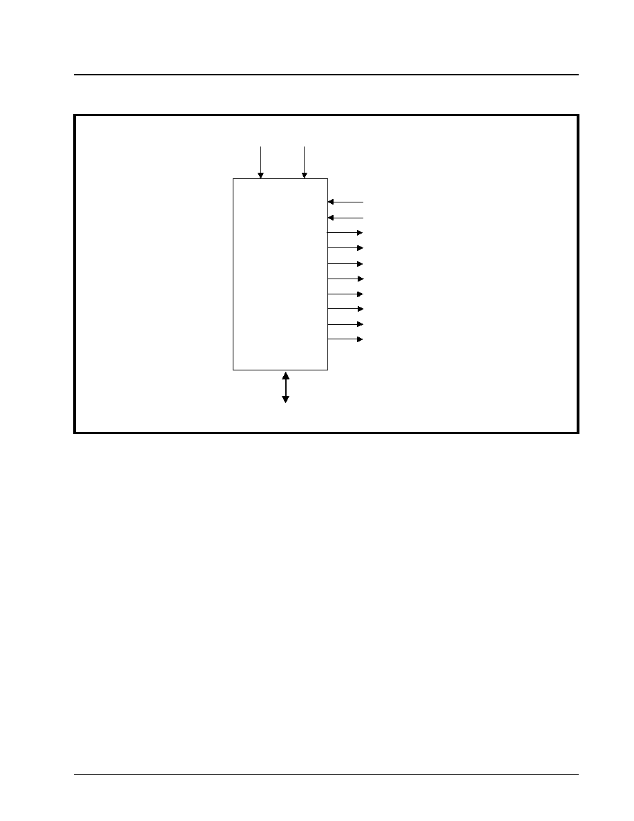
·Á
·Á
·Á
·Á
DS3 UNI FOR ATM
XRT7245
PRELIMINARY
REV. 1.03
215
F
IGURE
60. B
LOCK
D
IAGRAM
OF
THE
R
ECEIVER
DS3 F
RAMER
,
WITH
ASSOCIATED
PINS
.
RxPOS
RxNEG
RxAIS
RxOHClk
RxOH
RxLOS
RxFrame
RxOOF
RxLOF
Rx Framer
From DS3 LIU From DS3 LIU
To PLCP Processor
RxLineClk
From DS3 LIU
RLOS
From DS3 LIU
RxOHFrame
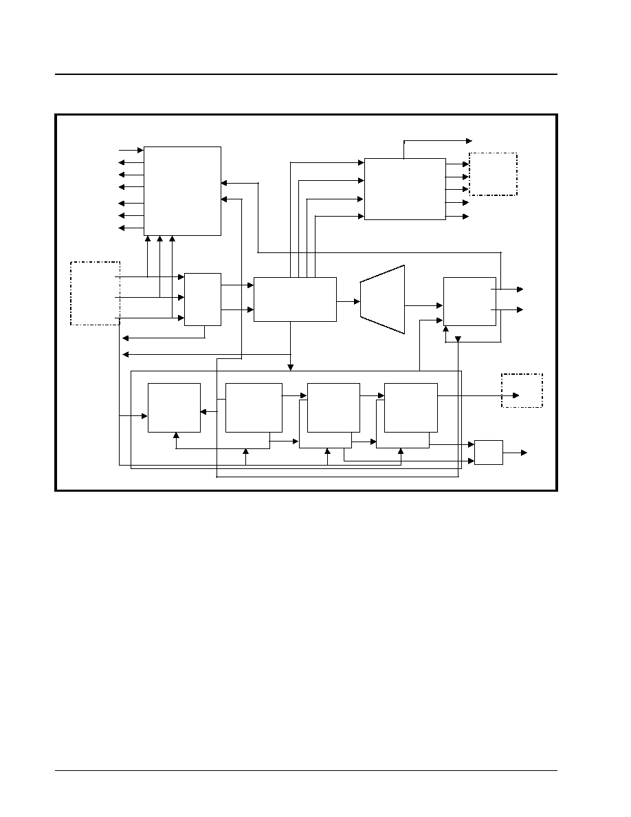
XRT7245
DS3 UNI FOR ATM
·Á
·Á
·Á
·Á
PRELIMINARY
REV. 1.03
216
7.1.2
Detailed Functional Description of the
Receive DS3 Framer
7.1.2.1
Receiving and Decoding Incoming
DS3 Data--via DS3 Line
The Receive DS3 Framer will receive timing and data
information from the incoming DS3 data stream.
The DS3 Timing information will be received via the
RxLineClk input pin; and the DS3 data information
will be received via the RxPOS and RxNEG input pins.
The Receive DS3 Framer is capable of receiving DS3
data pulses in unipolar or bipolar format. If the
Receive DS3 framer is operating in the bipolar for-
mat, then it can be configured to decode either AMI
or B3ZS line code data. Each of these input formats
and line codes will be discussed in detail, below.
7.1.2.1.1
Unipolar Coding
If the Receive DS3 Framer is operating in the Unipolar
mode, then it will receive the Single Rail NRZ DS3
data pulses via the RxPOS input pin. The Receive
DS3 Framer will also receive its timing signal via the
RxLineClk signal. No data pulses will be applied to
the RxNEG input pin. The Receive DS3 Framer
receives a logic "1" when a logic "1" level signal is
present at the RxPOS pin, during the sampling edge
of the RxLineClk signal. Likewise, a logic "0" is
received when a logic "0" level signal is applied to the
RxPOS pin. Figure 62 presents an illustration of the
behavior of the RxPOS, RxNEG and RxLineClk pins
when the UNI is operating in the Unipolar mode.
F
IGURE
61. F
UNCTIONAL
B
LOCK
D
IAGRAM
OF
R
ECEIVER
F
RAMER
Over Head
Processor
Frame Synchronizer
B3ZS
Decoder
Serial/Nibble
Converter
PayLoad
Overhead
MUX
Line Detector
ExtLOS
LOS Interrupt
AIS Interrupt
Idle Interrupt
RxAIS
RxLOS
RxIdle
RxPOS
RxNEG
RxLineClk
RxInFrame
RxFrame
RxOHFrame
RxOHClk
SubFrame
Counter
(Divide by 4)
Nibble
Counter
(Divide by 4)
Packet
Counter
(Divide by 85)
Frame
Counter
(Divide by 7)
Justify
RxFrame
OR
Gate
LCV Error
(to PMON)
RxNBClk
RxNBData
RxOFF
RxOOF
RxNBDat[4]
RxNBClk
New Frame
Alignment
Interrupt
To
Int
Block
Timing & Control
RxLineClk
PayLoad
Data
Enable
Enable
Interrupt from OH
Processor
RxOHFrame
RxOHClk
RxOH
RxFEBE
RxFrame
(To Tx
Framer)
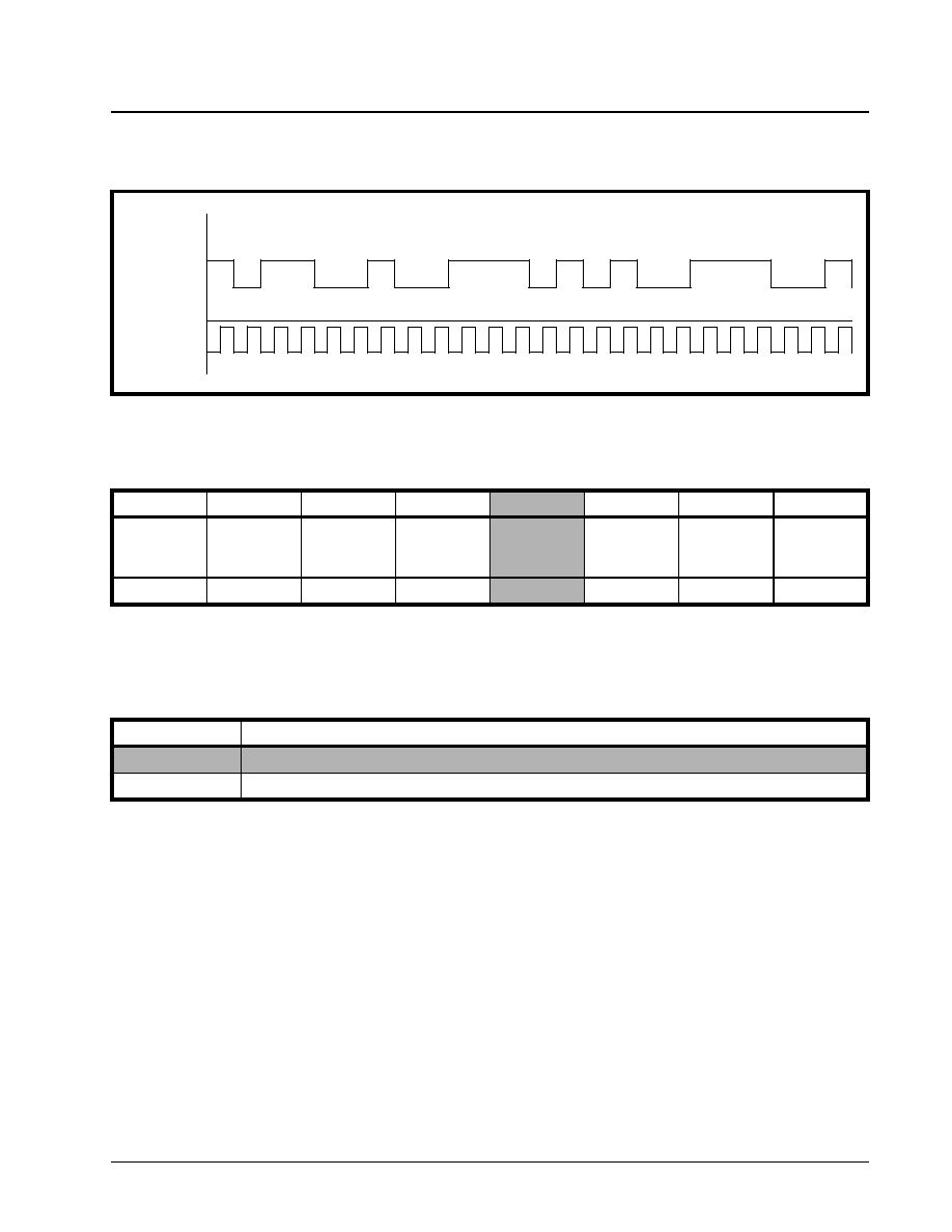
·Á
·Á
·Á
·Á
DS3 UNI FOR ATM
XRT7245
PRELIMINARY
REV. 1.03
217
The user can configure the Receive DS3 Framer to
operate in either the Unipolar or the Bipolar Mode by
writing the appropriate data to the UNI I/O Control
Register, as depicted below.
The following table relates the value of this bit-field to
the Receive DS3 Framer I/O Mode.
Note:
1. The default condition is the Bipolar Mode.
2. This selection also affects the Transmit DS3
Framer Line Interface Output Mode
7.1.2.1.2
Bipolar Decoding
If the Receive DS3 Framer is operating in the Bipolar
Mode, then it will receive the DS3 data pulses via
both the RxPOS, RxNEG, and the RxLineClk pins.
Figure 63 presents a circuit diagram illustrating how
the Receive DS3 Framer interfaces to the Line Inter-
face Unit while the UNI is operating in Bipolar mode.
The Receive DS3 Framer can be configured to
decode either the AMI or B3ZS line codes.
F
IGURE
62. B
EHAVIOR
OF
THE
R
X
POS, R
X
NEG
AND
R
X
L
INE
C
LK
SIGNALS
DURING
DATA
RECEPTION
OF
U
NIPOLAR
D
ATA
RxPOS
RxNEG
RxLineClk
Data
1
0
1
1
0
0
1
0
0
1
0
1
1
0
0
1
1
1
1
1
0
0
0
1
UNI I/O Control Register (Address = 01h)
B
IT
7
B
IT
6
B
IT
5
B
IT
4
B
IT
3
B
IT
2
B
IT
1
B
IT
0
LOC Enable
Test PMON
Interrupt
Enable
Reset
AMI/B3ZS*
Unipolar/
Bipolar*
TxClk Inv
RxClk Inv
Reframe
R/W
R/W
R/W
R/W
R/W
R/W
R/W
R/W
T
ABLE
44: T
HE
R
ELATIONSHIP
BETWEEN
THE
CONTENTS
OF
B
IT
3 (U
NIPOLAR
/B
IPOLAR
*)
WITHIN
THE
UNI I/O
C
ONTROL
R
EGISTER
AND
THE
RESULTING
R
ECEIVE
DS3 F
RAMER
L
INE
I
NTERFACE
I
NPUT
M
ODE
B
IT
3
R
ECEIVE
DS3 F
RAMER
L
INE
I
NTERFACE
I
NPUT
M
ODE
0
Bipolar Mode (Dual Rail): AMI or B3ZS Line Codes are Transmitted and Received.
1
Unipolar Mode (Single Rail) mode of transmission and reception of DS3 data is selected.
XRT7245
DS3 UNI FOR ATM
·Á
·Á
·Á
·Á
PRELIMINARY
REV. 1.03
218
7.1.2.1.2.1
AMI Decoding
AMI or Alternate Mark Inversion, means that consecu-
tive "one's" pulses (or marks) will be of opposite polarity
with respect to each other. This line code involves the
use of three different amplitude levels: +1, 0, and -1.
The +1 and -1 amplitude signals are used to represent
one's (or mark) pulses and the "0" amplitude pulses
(or the absence of a pulse) are used to represent
zeros (or space) pulses. The general rule for AMI is:
if a given "mark" pulse is of positive polarity, then the
very next "mark" pulse will be of negative polarity and
vice versa. This alternating-polarity relationship ex-
ists between two consecutive mark pulses, indepen-
dent of the number of zeros that exist between these
two pulses. Figure 64 presents an illustration of the
AMI Line Code as would appear at the RxPOS and
RxNEG pins of the UNI, as well as the output signal
on the line.
F
IGURE
63. I
LLUSTRATION
ON
HOW
THE
R
ECEIVE
DS3 F
RAMER
INTERFACES
TO
THE
L
INE
I
NTERFACE
U
NIT
,
WHILE
THE
UNI
IS
OPERATING
IN
B
IPOLAR
M
ODE
.

·Á
·Á
·Á
·Á
DS3 UNI FOR ATM
XRT7245
PRELIMINARY
REV. 1.03
219
Note: one of the reasons that the AMI Line Code has been
chosen for driving copper medium, isolated via transform-
ers, is that this line code has no dc component; thereby
eliminating dc distortion in the line.
7.1.2.1.2.2
B3ZS Decoding
The Transmit DS3 Framer and the associated LIU
embed and combine the data and clocking informa-
tion into the line signal that is transmitted to the
"far-end" equipment. The "far-end" equipment has
the task of recovering this data and timing informa-
tion from the incoming DS3 data stream. Most clock
and data recovery schemes rely on the use of
Phase-Locked-Loop technology. One of the problems
of using Phase-Locked-Loop (PLL) technology for
clock recovery is that it relies on transitions in the line
signal, in order to maintain lock with the incoming
DS3 data-stream. Therefore, these clock recovery
scheme, are vulnerable to the occurrence of a long
stream of consecutive zeros (e.g., no transitions in
the line). This scenario can cause the PLL to lose
"lock" with the incoming DS3 data, thereby causing
the "clock" and data recovery process of the receiver
to fail. Therefore, some approach is needed to insure
that such a long string of consecutive zeros can never
happen. One such technique is B3ZS (or Bipolar 3
Zero Substitution) encoding.
In general the B3ZS line code behaves just like AMI;
with the exception of the case when a long string of
consecutive zeros occurs on the line. Any 3 consecu-
tive zeros will be replaced with either a "00V" or a
"B0V" where "B" refers to a Bipolar pulse (e.g., a
pulse with a polarity that is compliant with the AMI
coding rule). And "V" refers to a Bipolar Violation pulse
(e.g., a pulse with a polarity that violates the alternating
polarity scheme of AMI.) The decision between insert-
ing an "00V" or a "B0V" is made to insure that an odd
number of Bipolar (B) pulses exist between any two
Bipolar Violation (V) pulses. The Receive DS3 Framer,
when operating with the B3ZS Line Code is responsi-
ble for decoding the B3ZS-encoded data back into a
unipolar (binary-format). For instance, if the Receive
DS3 Framer detects a "00V" or a "B0V" pattern in the
incoming pattern, the Receive DS3 Framer will replace
it with three consecutive zeros. Figure 65 presents a
timing diagram that illustrates examples of B3ZS
decoding.
F
IGURE
64. I
LLUSTRATION
OF
AMI L
INE
C
ODE
Data
RxPOS
RxNEG
Line Signal
1 0
1 1
0 0
0
1
0
1 1
1
0
1
0 1
0
0 1
1 0 0
1
1
1
0
0
1
F
IGURE
65. I
LLUSTRATION
OF
TWO
EXAMPLES
OF
B3ZS D
ECODING
Data
RxPOS
RxNEG
0 0 V
Line Signal
B 0 V
1 0
1 1
0 0
0
1
0
1 1
1
0
1
0 1
0
0 1
1
1 0
1
1
1
0
0 1
XRT7245
DS3 UNI FOR ATM
·Á
·Á
·Á
·Á
PRELIMINARY
REV. 1.03
220
7.1.2.1.2.3
Line Code Violations
The Receive DS3 Framer will also check the incoming
DS3 data stream for line code violations. For example,
when the Receive DS3 Framer detects a valid bipolar
violation (e.g., in B3ZS line code), it will substitute
three zeros into the binary data stream. However, if
the bipolar violation is invalid, then an LCV (Line Code
Violation) is flagged and the PMON LCV Event Count
Register (Address = 20h and 21h) is incremented.
Additionally, the LCV-One Second Accumulation
Registers will be incremented. For example: if the
incoming DS3 data is B3ZS encoded, the Receive
DS3 Framer will also increment the LCV One Second
Accumulation Register if three (or more) consecutive
zeros are received.
7.1.2.1.2.4
Receive Line Input Clocking
The incoming unipolar or bipolar data, applied to the
RxPOS and the RxNEG input pins are clocked into
the Receive DS3 Framer via the RxLineClk signal.
The UNI allows the user to specify which edge (e.g,
rising or falling) of the RxLineClk signal will sample
and latch the signal at the RxPOS and RxNEG input
signals into the UNI. The user can make this selection
by writing the appropriate data to bit 1 of the UNI I/O
Control Register, as depicted below.
The following table depicts the relationship between
the value of this bit-field to the sampling clock edge of
RxLineClk.
Figure 66 and 67 presents the Waveform and Timing
Relationships between RxLineClk, RxPOS and RxNEG
for each of these configurations.
UNI I/O Control Register (Address = 01h)
B
IT
7
B
IT
6
B
IT
5
B
IT
4
B
IT
3
B
IT
2
B
IT
1
B
IT
0
LOC
Enable
Test
PMON
IntEn
Reset
AMI/B3ZS*
Unipolar/
Bipolar*
TxLine
Clk Inv
RxLine
Clk Inv
Reframe
R/W
R/W
R/W
R/W
R/W
R/W
R/W
R/W
T
ABLE
45: T
HE
R
ELATIONSHIP
BETWEEN
THE
CONTENTS
OF
B
IT
1 (R
X
L
INE
C
LK
I
NV
)
OF
THE
UNI I/O C
ONTROL
R
EGISTER
,
AND
THE
SAMPLING
EDGE
OF
THE
R
X
L
INE
C
LK
SIGNAL
R
X
C
LK
I
NV
(B
IT
1)
R
ESULT
0
Rising Edge: RxPOS and RxNEG are sampled at the rising edge of RxLineClk. See Figure 66 for
timing relationship between RxLineClk, RxPOS, and RxNEG.
1
Falling Edge: RxPOS and RxNEG are sampled at the falling edge of RxLineClk. See Figure 67 for
timing relationship between RxLineClk, RxPOS, and RxNEG.

·Á
·Á
·Á
·Á
DS3 UNI FOR ATM
XRT7245
PRELIMINARY
REV. 1.03
221
7.1.2.2
DS3 Frame Synchronization
Once the B3ZS (or AMI) encoded data has been de-
coded into a binary data-stream, the Frame Synchroni-
zation section of the Receive DS3 Framer will use
portions of this data-stream in order to synchronize
itself to the "Far-End" Transmit DS3 Framer. At any
given time, the Frame Synchronization section of the
Receive DS3 Framer will be operating in one of two
modes.
∑ The Frame Acquisition Mode:
In this mode, the
Receive DS3 Framer is trying to acquire synchroni-
zation with the incoming DS3 frame, or
∑
The Frame Maintenance Mode:
In this mode, the
Receive DS3 Framer is trying to maintain frame
synchronization with the incoming DS3 Frames.
Figure 68 presents a State Machine diagram that
depicts the Receive DS3 Framer's "DS3 Frame
Acquisition/Maintenance" Algorithm.
F
IGURE
66. W
AVEFORM
/T
IMING
R
ELATIONSHIP
BETWEEN
R
X
L
INE
C
LK
, R
X
POS
AND
R
X
NEG--W
HEN
R
X
POS
AND
R
X
NEG
ARE
TO
BE
SAMPLED
ON
THE
RISING
EDGE
OF
R
X
L
INE
C
LK
RxLineClk
RxPOS
RxNEG
t38
t39
t42
F
IGURE
67. W
AVEFORM
/T
IMING
R
ELATIONSHIP
BETWEEN
R
X
L
INE
C
LK
, R
X
POS
AND
R
X
NEG--W
HEN
R
X
POS
AND
R
X
NEG
ARE
TO
BE
SAMPLED
ON
THE
FALLING
EDGE
OF
R
X
L
INE
C
LK
RxLineClk
RxPOS
RxNEG
t40
t41
XRT7245
DS3 UNI FOR ATM
·Á
·Á
·Á
·Á
PRELIMINARY
REV. 1.03
222
7.1.2.2.1
The Framing Acquisition Mode
The Receive DS3 Framer will be performing "Frame
Acquisition" operation while it is operating in the
following states (per the "DS3 Frame Acquisition/
Maintenance" algorithm State Machine diagram,
as depicted in Figure 68.)
∑
F-bit Search
∑
M-bit Search
∑ Parity Check (optional)
Once the Receive DS3 Framer enters the "In-Frame"
state (per Figure 60), then it will begin "Frame Main-
tenance" operation.
When the Receive DS3 Framer is in the "frame-
acquisition" mode, it will begin to look for valid DS3
frames by first searching for the F-bits. At this "initial
point" the Receive DS3 Framer will be operating in the
"F-Bit Search" state within the "DS3 Frame Acquisition/
Maintenance" algorithm state machine diagram (see
Figure 68). Recall from the discussion in Section 6.4.2,
that each DS3 F-frame consists of four (4) F-bits that
occur in a repeating "1001" pattern. The Receive
DS3 Framer will attempt to locate this F-bit pattern by
performing five (5) different searches in parallel. The
F-bit search has been declared successful if at least
10 consecutive F-bits are detected. After the F-bit
match has been declared, the Receive DS3 Framer
will then transition to the "M-Bit Search" state within
the "DS3 Frame Acquisition/Maintenance" algorithm
(per Figure 68). When the Receive DS3 Framer
reaches this state, it will begin searching for valid
M-bits. Recall from the discussion in Section 6.4.2
that each DS3 M-frame consists of three (3) M-bits
that occur in a repeating "010" pattern. The M-bit
search is declared successful if three consecutive
M-frames (or 21 F-frames) are detected correctly.
Once this occurs an "M-frame lock" is declared, and
F
IGURE
68. T
HE
S
TATE
M
ACHINE
D
IAGRAM
FOR
THE
R
ECEIVE
DS3 F
RAMER
'
S
"F
RAME
A
CQUISITION
/
M
AINTENANCE
" A
LGORITHM
F-Bit Search
M-Bit Search
F-Bit Synch
Achieved
In-Frame
RxOOF pin
is Negated.
10 Consecutive F-bits
Correctly Received
Parity Check
(Only if Framing
on Parity is
Selected)
M-bits Correctly
Detected for 3
Consecutive M-Frames
(Framing on Parity is
Selected)
M-bits Correctly
Detected for 3
Consecutive M-Frames
(Framing on Parity is
Not Selected)
OOF Criteria
based upon values
for F-Sync Algo
and M-Sync Algo
Valid Parity
Parity Error in
2 out of 5 frames
·Á
·Á
·Á
·Á
DS3 UNI FOR ATM
XRT7245
PRELIMINARY
REV. 1.03
223
the Receive DS3 Framer will then transition to the
"In-Frame" state. At this point, the Receive DS3
Framer will declare itself in the "In-Frame" condition,
and will begin "Frame Maintenance" operations. The
Receive DS3 Framer will then indicate that it has tran-
sitioned from the "OOF" condition into the "In-Frame"
condition by doing the following.
∑
Generate a "Change in OOF Condition" interrupt to
the local µP.
∑
Negate the RxOOF output pin (e.g., toggle it "low").
∑ Negate the "Rx OOF" bit-field (Bit 4) within the
Receive DS3 Configuration and Status Register.
The user can configure the Receive DS3 Framer to
operate such that `valid parity' (P-bits) must also be
detected before the Receive DS3 Framer can declare
itself "In Frame". The user can set this configuration
by writing the appropriate data to the Rx DS3 Config-
uration and Status Register, as depicted below.
The following table relates the contents of this bit field
to the framing acquisition criteria.
Once the Receive DS3 Framer is in the "In-Frame"
condition, normal data recovery and processing of
the DS3 data stream begins. The maximum average
reframing time is less than 1.5 ms.
7.1.2.2.2
The Framing Maintenance Mode
When the Receive DS3 Framer is operating in the
"In-Frame" state (per Figure 68), it will then begin to
perform "Frame Maintenance" operations; where it
will continue to verify that the F- and M-bits are
present, at their proper locations. While the Receive
DS3 Framer is operating in the "Frame Maintenance"
mode, it will declare an "Out-of-Frame" (OOF) condi-
tion if 3 or 6 F-bits (depending upon user selection)
out of 16 consecutive F-bits are in error. The user
makes this selection for the "OOF Declaration" criteria
by writing the appropriate value to bit 1 (F-Sync Algo)
of the Rx DS3 Configuration and Status Register, as
depicted below.
Rx DS3 Configuration and Status Register, (Address = 0Eh)
B
IT
7
B
IT
6
B
IT
5
B
IT
4
B
IT
3
B
IT
2
B
IT
1
B
IT
0
Rx AIS
Rx LOS
Rx Idle
Rx OOF
Int LOS
Disable
Framing on
Parity
F-Sync Algo
M-Sync Algo
RO
RO
RO
RO
R/W
R/W
R/W
R/W
T
ABLE
46: T
HE
R
ELATIONSHIP
BETWEEN
THE
CONTENTS
OF
B
IT
2 (F
RAMING
ON
P
ARITY
)
WITHIN
THE
R
X
DS3
C
ONFIGURATION
AND
S
TATUS
R
EGISTER
,
AND
THE
RESULTING
"F
RAMING
A
CQUISITION
C
RITERIA
"
F
RAMING
ON
P
ARITY
(B
IT
2)
F
RAMING
A
CQUISITION
C
RITERIA
0
The "In-frame" is declared after F-bit synchronization (10 F-bit matches) followed by M-bit
synchronization (M-bit matches for 3 DS3 M-frames)
1
The "In-frame" condition is declared after F-bit synchronization, followed by M-bit syn-
chronization, with valid parity over the frames. Also, the occurrence of parity errors in 2
or more out of 5 frames starts a frame search
Rx DS3 Configuration and Status Register, (Address = 0Eh)
B
IT
7
B
IT
6
B
IT
5
B
IT
4
B
IT
3
B
IT
2
B
IT
1
B
IT
0
Rx AIS
Rx LOS
Rx Idle
Rx OOF
Int LOS
Disable
Framing on
Parity
F-Sync
Algo
M-Sync
Algo
RO
RO
RO
RO
R/W
R/W
R/W
R/W

XRT7245
DS3 UNI FOR ATM
·Á
·Á
·Á
·Á
PRELIMINARY
REV. 1.03
224
The following table relates the contents of this bit-
field to the "OOF Declaration" criteria
Note: Once the Receive DS3 Framer has declared an
"OOF" condition, it will transition back to the "F-Bit Search"
state within the "DS3 Frame Acquisition/Maintenance"
algorithm (per Figure 68).
In addition to selecting an "OOF Declaration" criteria
for the F-bits, the user has two options for configuring
the "OOF Declaration" criteria based upon M-bits.
1.
M-bit errors do not cause a "OOF" Declaration, or
2.
"OOF" will be declared if 3 out of 4 consecutive
M-bits are in error.
The user will select between these two options by
writing the appropriate value to Bit 0 (M-Sync Algo) of
the Receive DS3 Configuration and Status Register;
as depicted below.
The following table relates the contents of this Bit
Field to the M-Bit Error criteria for Declaration of OOF
The "Framing on Parity" Option
Finally, the UNI offers the "Framing on Parity" option,
which also effects the "OOF Declaration" criteria. As
was mentioned earlier, the UNI allows the user to
configure the Receive DS3 Framer to detect `valid-
parity' before declaring itself "In-Frame". This same
selection allows the Receive DS3 Framer to also de-
clare an "OOF Condition" if a P-bit error is detected in
2 of the last 5 M-frames.
Whenever the Receive DS3 Framer declares "OOF"
after being in the "In-Frame" State the following will
happen.
∑
The Receive DS3 Framer will assert the RxOOF
output pin (e.g., toggles it "high").
∑
Bit 4 of the Rx DS3 Configuration and Status
Register will be set to "1" as depicted below.
T
ABLE
47: T
HE
R
ELATIONSHIP
BETWEEN
THE
CONTENTS
OF
B
IT
1 (F-S
YNC
A
LGO
)
WITHIN
THE
R
X
DS3
C
ONFIGURATION
AND
S
TATUS
R
EGISTER
,
AND
THE
RESULTING
"F-
BIT
OOF D
ECLARATION
CRITERIA
"
FOR
THE
R
ECEIVE
DS3 F
RAMER
F-S
YNC
A
LGO
(B
IT
1)
OOF D
ECLARATION
C
RITERIA
0
"OOF" is declared when 6 out of 16 consecutive F-bits are in error.
1
"OOF" is declared when 3 out of 16 consecutive F-bits are in error.
Rx DS3 Configuration and Status Register, (Address = 0Eh)
B
IT
7
B
IT
6
B
IT
5
B
IT
4
B
IT
3
B
IT
2
B
IT
1
B
IT
0
Rx AIS
Rx LOS
Rx Idle
Rx OOF
Int LOS
Disable
Framing on
Parity
F-Sync
Algo
M-Sync
Algo
RO
RO
RO
RO
R/W
R/W
R/W
R/W
T
ABLE
48: T
HE
R
ELATIONSHIP
BETWEEN
THE
CONTENTS
OF
B
IT
0 (M-S
YNC
A
LGO
)
WITHIN
THE
R
X
DS3
C
ONFIGURATION
AND
S
TATUS
R
EGISTER
,
AND
THE
RESULTING
"M-B
IT
OOF D
ECLARATION
C
RITERIA
"
FOR
THE
R
ECEIVE
DS3 F
RAMER
MS
YNC
A
LGO
OOF D
ECLARATION
C
RITERIA
0
M-Bit Errors do not result in the declaration of "OOF"
1
"OOF" is declared when 3 out of 4 M-bits are in error.
Rx DS3 Configuration and Status Register, (Address = 0Eh)
B
IT
7
B
IT
6
B
IT
5
B
IT
4
B
IT
3
B
IT
2
B
IT
1
B
IT
0
Rx AIS
Rx LOS
Rx Idle
Rx OOF
Int LOS Disable
Framing on Parity
F-Sync Algo M-Sync Algo
X
X
X
1
X
X
X
X
·Á
·Á
·Á
·Á
DS3 UNI FOR ATM
XRT7245
PRELIMINARY
REV. 1.03
225
∑
The Receive DS3 Framer will also issue a "Change
in OOF Status" interrupt request, anytime there is a
change in the "OOF" status.
7.1.2.2.3
Forcing a Reframe via Software
Command
The UNI allows the user to command a reframe pro-
cedure with the Receive DS3 Framer via software
command. If the user writes a "1" into Bit 0 of the UNI
I/O Control Register, as depicted below; then the
Receive DS3 Framer will be forced into the Frame
Acquisition Mode, (or more specifically, in the "F-Bit
Search State" per Figure 68) and will begin its search
for valid F-Bits. The UNI will also respond to this
command by asserting the RxOOF output pin, and
generating a "Change in OOF Status" interrupt.
7.1.2.2.4
Performance Monitoring of the Frame
Synchronization section of the
Receive DS3 Framer
The user can monitor the number of framing bit
errors (M and F bits) that have been detected by the
Receive DS3 Framer. This is accomplished by peri-
odically reading the PMON Framing Bit Error Count
Registers (Address = 22h and 23h), as depicted below.
When the local µP/µC reads these registers, it will
read in the number of framing bit errors that have
been detected since the last read of these two regis-
ters. These registers are reset upon read.
7.1.2.3
DS3 Receive Alarms
7.1.2.3.1
Loss of Signal (LOS) Alarm
The Receive DS3 Framer will declare a "Loss of Signal"
(LOS) state when it detects 180 consecutive incom-
ing "0s" via the RxPOS and RxNEG input pins or if
the RLOS input pin (from the XRT7295 DS3 Line Re-
ceiver IC) is asserted. The Receive DS3 Framer will
indicate the occurrence of an LOS condition by:
∑
Asserting the RxLOS output pin (e.g., toggles it
"high").
∑
Setting Bit 6 of the Rx DS3 Configuration and Status
Register to "1", as depicted below.
UNI I/O Control Register (Address = 01h)
B
IT
7
B
IT
6
B
IT
5
B
IT
4
B
IT
3
B
IT
2
B
IT
1
B
IT
0
LOC Enable
Test PMON
IntEn Reset
AMI
Unipolar
TxClk Inv
RxClk Inv
Reframe
R/W
R/W
R/W
R/W
R/W
R/W
R/W
R/W
Address = 22h, PMON Framing Bit Error Event Count Register--MSB
B
IT
7
B
IT
6
B
IT
5
B
IT
4
B
IT
3
B
IT
2
B
IT
1
B
IT
0
F-Bit Error Count--High Byte
RO
RO
RO
RO
RO
RO
RO
RO
0
0
0
0
0
0
0
0
Address = 23h, PMON Framing Bit Error Event Count Register--LSB
B
IT
7
B
IT
6
B
IT
5
B
IT
4
B
IT
3
B
IT
2
B
IT
1
B
IT
0
F-Bit Error Count--Low Byte
RO
RO
RO
RO
RO
RO
RO
RO
0
0
0
0
0
0
0
0
Rx DS3 Configuration and Status Register, (Address = 0Eh)
B
IT
7
B
IT
6
B
IT
5
B
IT
4
B
IT
3
B
IT
2
B
IT
1
B
IT
0
Rx AIS
Rx LOS
Rx Idle
Rx OOF
Int LOS Disable
Framing on Parity
F-Sync Algo
M-Sync Algo
X
1
X
X
X
X
X
X
XRT7245
DS3 UNI FOR ATM
·Á
·Á
·Á
·Á
PRELIMINARY
REV. 1.03
226
∑
The Receive DS3 Framer will generate a "Change
in LOS Status" interrupt request. (
Note:
The
Receive DS3 Framer will also declare an "OOF"
condition and perform all of the "notification proce-
dures" as described in Section 7.1.2.2.2).
The Receive DS3 Framer will negate the "LOS" con-
dition when at least 60 out of 180 consecutive re-
ceived bits are "1".
Note: The Receive DS3 Framer will also generate the
"Change in LOS Condition" interrupt, when it negates the
LOS Condition.
The UNI chip allows the user to change the "LOS
Declaration criteria" such that an LOS condition is
declared only if the RLOS input pin (from the XRT7295
DS3 Line Receiver IC) is asserted. The "internally-
generated" LOS criteria of "180 consecutive 0s" will
be disabled. The user can accomplish this by writing
a "1" to bit 3 of the Rx DS3 Configuration and Status
Register, as depicted below.
Note: For more information on the RLOS input pin, please
see Section 5.0.
7.1.2.3.2
Alarm Indication Signal (AIS)
The Receive DS3 Framer will identify and declare an
"AIS" condition if it detects all of the following condi-
tions in the incoming DS3 Data Stream:
∑
Valid M-bits, F-bits and P-bits
∑
All C-bits are zeros.
∑
X-bits are set to "1"
∑ The Payload portion of the DS3 Frame exhibits a
repeating "1010..." pattern
The Receive DS3 Framer contains, within its circuitry,
an Up/Down Counter that supports the "assertion"
and "negation" of the AIS condition. The counter
begins with the value of 00h upon power up or reset.
The counter is then incremented anytime the Receive
DS3 Framer detects an "AIS Type" M-frame. This
counter is then decremented, or kept at "zero" value,
when the Receive DS3 Framer detects a "non-AIS"
type M-frame. The Receive DS3 Framer will declare
an "AIS Condition" if this counter reaches the value of
63 M-frames or greater. Explained another way, the
AIS condition is declared if the number of AIS-type
M-frames is detected, such that it meets the following
conditions:
N
AIS
- N
VALID
S 63
where N
AIS
= the number of M-frames containing the
AIS pattern.
N
VALID
= the number of M-frames not containing the
AIS pattern
If at anytime, the contents of this Up/Down counter
exceeds 63 M-frames, then the Rx DS3 Framer will:
∑
Assert the RxAIS output pin.
∑
Set Bit 7 of the Rx DS3 Configuration and Status
Register, as depicted below.
∑ Generate a "Change in AIS Status" Interrupt
Request to the local µP/µC.
The Receive DS3 Framer will negate the "AIS" condi-
tion when the following expression is true.
N
AIS
- N
VALID
µ 0.
In other words, once the Receive DS3 Framer has
detected a sufficient number of normal (or "Non-AIS")
M-frames, such that this "Up/Down" counter reaches
"zero", then the Receive DS3 Framer will negate the
"AIS Condition" indicators. The Receive DS3 Framer
will inform the local µC/µP of this negation of the "AIS
Status" by generating a "Change in AIS Status"
interrupt.
Rx DS3 Configuration and Status Register, (Address = 0Eh)
B
IT
7
B
IT
6
B
IT
5
B
IT
4
B
IT
3
B
IT
2
B
IT
1
B
IT
0
Rx AIS
Rx LOS
Rx Idle
Rx OOF
Int LOS Disable
Framing on Parity
F-Sync Algo M-Sync Algo
RO
RO
RO
RO
R/W
R/W
R/W
R/W
Rx DS3 Configuration and Status Register, (Address = 0Eh)
B
IT
7
B
IT
6
B
IT
5
B
IT
4
B
IT
3
B
IT
2
B
IT
1
B
IT
0
Rx AIS
Rx LOS
Rx Idle
Rx OOF
Int LOS Disable
Framing on Parity
F-Sync Algo
M-Sync Algo
1
X
X
X
X
X
X
X
·Á
·Á
·Á
·Á
DS3 UNI FOR ATM
XRT7245
PRELIMINARY
REV. 1.03
227
7.1.2.3.3
Idle (Condition) Alarm
The Receive DS3 Framer will identify and declare an
"Idle Condition" if it receives a sufficient number of
M-Frames that meets all of the following conditions.
∑
Valid M-bits, F-bits, and P-bits
∑
The 3 CP-bits (in F-Frame #3) are zeros.
∑
The X-bits are set to "1"
∑ The payload portion of the DS3 Frame exhibits a
repeating "1100..." pattern.
The Receive DS3 Framer circuitry includes an Up/
Down Counter that is used to track the number of
M-frames that are detected as exhibiting the "Idle
Condition" by the Receive DS3 Framer. The contents
of this counter is set to zero upon reset or power up.
This counter is then incremented whenever the
Receive DS3 Framer detects an "Idle-type" M-frame.
The counter is decremented, or kept at zero if a "non-
Idle" M-frame is detected. If the Receive DS3 Framer
detects a sufficient number of "Idle-type" M-frames,
such that the counter reaches the number "63", then
the Receive DS3 Framer will declare the "Idle Condi-
tion". Explained another way, the Receive DS3 Framer
will declare an "Idle Condition" if the number of "Idle-
Pattern" M-frames is detected such that it meets the
following conditions.
N
IDLE
- N
VALID
S 63,
where: N
IDLE
= the number of M-frames containing
"Idle Patterns"
N
VALID
= the number of M-frames not exhibiting the
"Idle Pattern"
Any time the contents of this "Up/Down" Counter
reaches the number 63, then the Receive DS3
Framer will:
∑
Set Bit 5 of the Rx DS3 Configuration and Status
Register, as depicted below.
∑ Generate a "Change in Idle Status" Interrupt
Request to the local µP/µC.
The Receive DS3 Framer will negate the "Idle Condi-
tion" if it has detected a sufficient number of "Non-Idle"
M-frames, such that this Up/Down Counter reaches
the value "0".
7.1.2.3.4
Detection of (FERF) Yellow Alarm
Condition
The Receive DS3 Framer will identify and declare a
"Yellow Alarm" condition or a "Far-End Receive Failure"
(FERF) condition, if it starts to receive DS3 frames
with all of its X-bits set to "0".
When the Receive DS3 Framer detects a "Yellow
Alarm" condition in the incoming DS3 frames, then it
will then do the following.
∑
It will assert the "RxFERF" (bit-field 4) within the Rx
DS3 Status Register, as depicted below.
This bit-field will remain asserted for the duration that
the "Yellow Alarm" condition exists.
∑
The Receive DS3 Framer will also generate a
"Change in FERF Status" interrupt to the local
µ
P/
µ
C.
Consequently, the Receive DS3 Framer will also
assert the "FERF Interrupt Status" bit, within the Rx
DS3 Interrupt Status Register, as depicted below.
Rx DS3 Configuration and Status Register, (Address = 0Eh)
B
IT
7
B
IT
6
B
IT
5
B
IT
4
B
IT
3
B
IT
2
B
IT
1
B
IT
0
Rx AIS
Rx LOS
Rx Idle
Rx OOF
Int LOS Disable
Framing on Parity
F-Sync Algo M-Sync Algo
X
X
1
X
X
X
X
X
Address = 0Fh, Rx DS3 Status Register
B
IT
7
B
IT
6
B
IT
5
B
IT
4
B
IT
3
B
IT
2
B
IT
1
B
IT
0
Unused
RxFERF
RxAIC
RxFEBE [2]
RxFEBE [1]
RxFEBE [0]
RO
RO
RO
RO
RO
RO
RO
RO
0
0
0
1
x
x
x
x

XRT7245
DS3 UNI FOR ATM
·Á
·Á
·Á
·Á
PRELIMINARY
REV. 1.03
228
7.1.2.4
Performance Monitoring of the DS3
Transport Medium
The DS3 Frame consists of some overhead bits that
are used to support performance monitoring of the
DS3 Transmission Link. These bits are the P-Bits and
the CP-Bits.
7.1.2.4.1
P-Bit Checking/Options
The "Far-End" Transmit DS3 Framer will compute the
even parity of the payload portion of a DS3 Frame
and will place the resulting parity bit value in the 2
P-bit-fields within the very next "outbound" DS3
Frame. The value of these two bits fields are expected
to be identical.
The Receive DS3 Framer, while receiving each of
these DS3 Frames (from the "Far-End" Transmit DS3
Framer), will compute the even-parity of the payload
portion of the frame. The Receive DS3 Framer will
then compare this "locally computed" parity value to
that of the P-bit fields within the very next DS3
Frame. If the Receive DS3 Framer detects a parity
error, then three things will happen:
1.
The Receive DS3 Framer will inform the local µP/
µC of this occurrence by generating a "Detection
of P-Bit Error" interrupt;
2.
The Receive DS3 Framer will alter the value of
the FEBE bits, (to a pattern other than "111") that
the "Near-End" Transmit DS3 Framer will be
transmitting back to the "Far-End" Terminal.
3.
The PMON Parity Error Event Count Registers
(Address = 24h and 25h) will be incremented for
each detected parity error, in the incoming DS3
data stream. The bit-format of these two regis-
ters follows.
When the local µP reads these registers, it will read
in the number of parity-bit errors that have been de-
tected by the Receive DS3 Framer, since the last
time these registers were read. These registers are
reset upon read.
Note: When the "Framing with Parity" option is selected,
the Receive DS3 Framer will declared an "OOF" condition if
P-bit errors were detected in two out of 5 consecutive DS3
M-frames.
Rx DS3 Interrupt Status Register (Address = 11h)
B
IT
7
B
IT
6
B
IT
5
B
IT
4
B
IT
3
B
IT
2
B
IT
1
B
IT
0
CP Bit RUR
Error
Interrupt
Status
LOS
Interrupt
Status
AIS Interrupt
Status
IDLE
Interrupt
Status
FERF
Interrupt
Status
AIC
Interrupt
Status
OOF
Interrupt
Status
Parity Error
Interrupt
Status
RO
RUR
RUR
RUR
RUR
RUR
RUR
RUR
0
x
x
x
1
x
x
x
Address = 24h, PMON Parity Error Event Count Register--MSB
B
IT
7
B
IT
6
B
IT
5
B
IT
4
B
IT
3
B
IT
2
B
IT
1
B
IT
0
Parity Error Count--High Byte
RO
RO
RO
RO
RO
RO
RO
RO
0
0
0
0
0
0
0
0
Address = 25h, PMON Parity Error Event Count Register--LSB
B
IT
7
B
IT
6
B
IT
5
B
IT
4
B
IT
3
B
IT
2
B
IT
1
B
IT
0
Parity Error Count--Low Byte
RO
RO
RO
RO
RO
RO
RO
RO
0
0
0
0
0
0
0
0
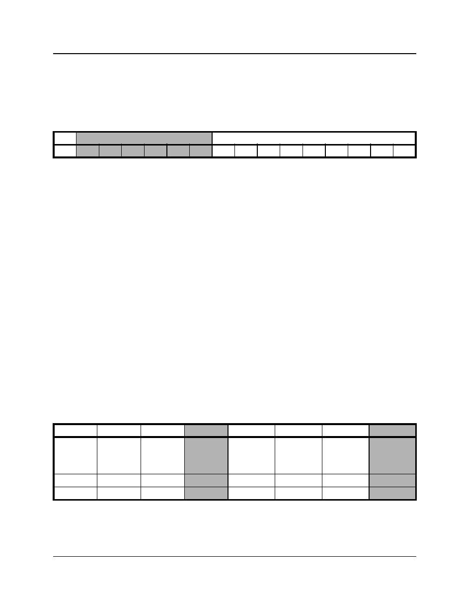
·Á
·Á
·Á
·Á
DS3 UNI FOR ATM
XRT7245
PRELIMINARY
REV. 1.03
229
7.1.2.4.2
CP-Bit Checking/Options
These parity bits are not processed by the Receiver
DS3 Framer.
7.1.2.5
The Receive FEAC Processor
If the Receive DS3 Framer is operating in the C-bit
Parity Mode, then the FEAC bit-field within the DS3
Frame can be used to receive FEAC (Far End Alarm
and Control) messages (See Figure 38). Each FEAC
code word is actually six bits in length. However, this
six bit FEAC Code word is encapsulated with 10
framing bits to form a 16 bit message of the form:
where "xxxxxx" is the FEAC Code word. The right-
most bit (e.g., a "1") will be received first. Since each
DS3 Frame contains only 1 FEAC bit-field, 16 DS3
Frames are required to transmit the 16 bit FEAC
code message. The six bits, labeled "x" can repre-
sent 64 distinct messages, of which 43 have been
defined in the standards.
The Receive FEAC Processor frames and "validates"
the incoming FEAC data from the "Far-End" Transmit
FEAC Processor via the received FEAC channel.
Additionally, the Receive FEAC Processor will write
the "Received FEAC" code words into an 8 bit
"Rx-FEAC" register. Framing is performed by looking
for two "0s" spaced 6 bits apart preceded by 8 "1s".
The Receive DS3 Framer contains two registers that
support FEAC Message Reception.
∑
Rx DS3 FEAC Register (Address = 12h)
∑ Rx DS3 FEAC Interrupt Enable/Status Register
(Address = 13h)
The Receive FEAC Processor generates an interrupt
upon "validation" and "removal" of the incoming
FEAC Code words.
Operation of the Receive DS3 FEAC Processor
The Receive FEAC Processor will "validate" or
"remove" FEAC code words that it receives from the
"Far End" Transmit FEAC Processor. The "FEAC
Code Validation" and "Removal" functions are
described below.
FEAC Code Validation
When the "Far-End" Transmit DS3 Framer wishes to
send a FEAC message to the "Near-End" Receive DS3
Framer, it (the "Far-End" Transmit DS3 Framer) will
transmit this 16 bit message, repeatedly for a total of
10 times. The Receive FEAC Processor will frame to
this incoming FEAC Code Message, and will attempt
to "validate" this message. Once the Receive FEAC
Processor has received the same FEAC code word
in at least 8 out of the last 10 received codes, it will
"validate" this code word by writing this 6 bit code word
into the Receive DS3 FEAC Register. The Receive
FEAC Processor will then inform the local µC/µP of
this "Receive FEAC validation" event by generating a
"Rx FEAC Valid" interrupt and asserting the "FEAC
Valid" and the Rx FEAC Valid Interrupt Status Bits in
the Rx DS3 Interrupt Enable/Status Register, as
depicted below. The Bit Format of the Rx DS3 FEAC
Register is presented below.
FEAC C
ODE
W
ORD
F
RAMING
0
x
x
x
x
x
x
0
1
1
1
1
1
1
1
1
Rx DS3 FEAC Interrupt Enable/Status Register (Address = 13h)
B
IT
7
B
IT
6
B
IT
5
B
IT
4
B
IT
3
B
IT
2
B
IT
1
B
IT
0
Unused
Unused
Unused
FEAC Valid
RxFEAC
Remove
Interrupt
Enable
RxFEAC
Remove
Interrupt
Status
RxFEAC
Valid
Interrupt
Enable
RxFEAC
Valid
Interrupt
Status
R/O
R/O
R/O
R/O
R/W
RUR
R/W
RUR
x
x
x
1
x
0
1
1
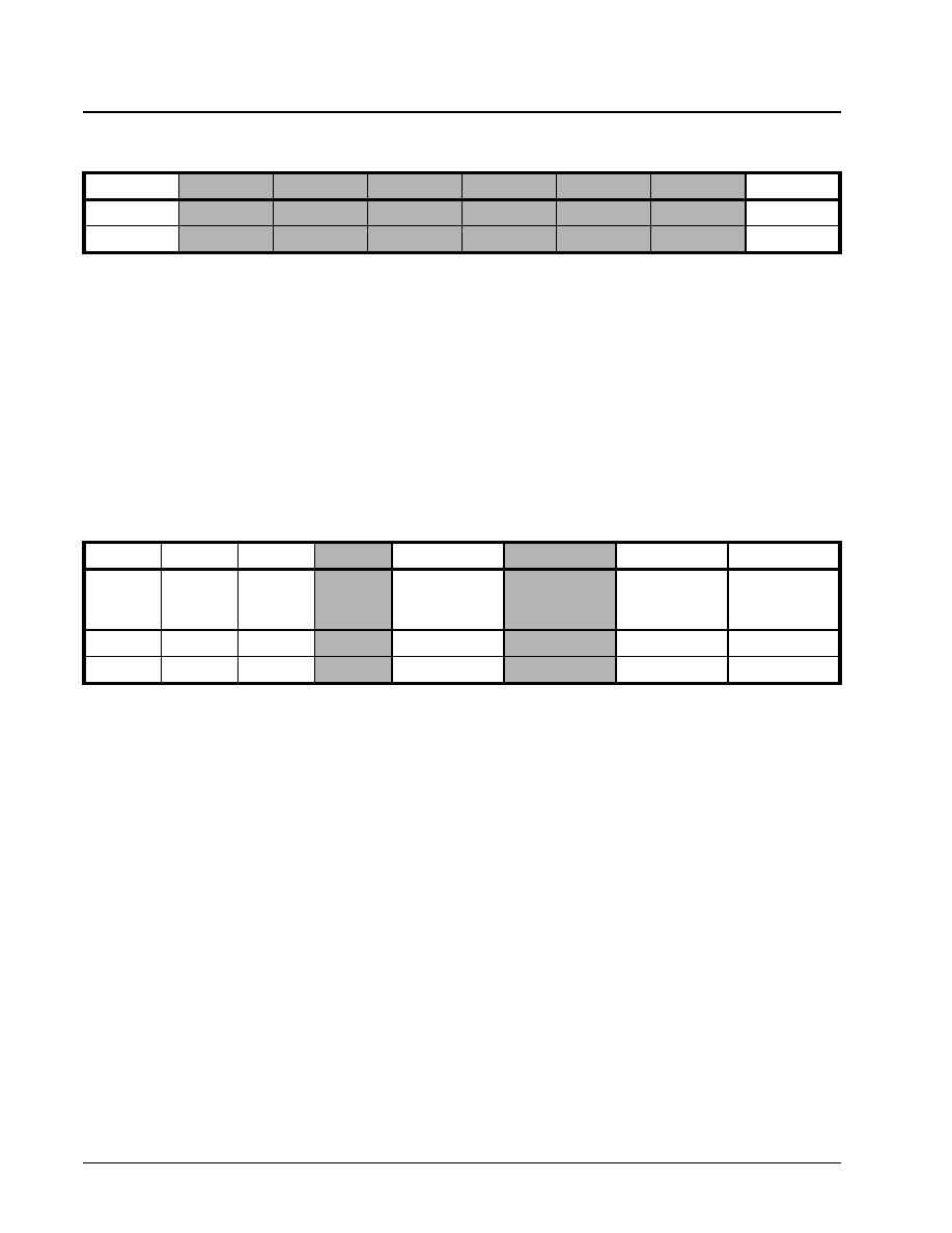
XRT7245
DS3 UNI FOR ATM
·Á
·Á
·Á
·Á
PRELIMINARY
REV. 1.03
230
The purpose of generating an interrupt to the local
µP, upon "FEAC Code Word Validation" is to inform
the local µP that the UNI has a "newly received"
FEAC message that needs to be read. The local µP
would read-in this FEAC code word from the Rx DS3
FEAC Register (Address = 12h).
FEAC Code Removal
After the 10th transmission of a given FEAC code
word, the "Far-End" Transmit DS3 Framer may start
to transmit a different FEAC code word. When the
Receive FEAC processor detects this occurrence, it
must "Remove" the FEAC codeword that is presently
residing in the Rx DS3 FEAC Register. The Receive
FEAC Processor will "remove" the existing FEAC
code word when it detects that 3 (or more) out of the
last 10 received FEAC codes are different from the
latest "validated" FEAC code word. The Receive
FEAC Processor will inform the local µP/µC of this
"removal" event by generating a "Rx FEAC Removal"
interrupt, and asserting the "RxFEAC Remove Inter-
rupt Status" bit in the Rx DS3 Interrupt Enable/Status
Register, as depicted below.
Additionally, the Receive FEAC processor will also
denote the "removal" event by setting the "FEAC Valid"
bit-field (Bit 4), within the Rx DS3 FEAC Interrupt
Enable/Status Register to "0", as depicted above.
The description of Bits 0 through 3 within this register,
all support Interrupt Processing, and will therefore be
presented in Section 7.1.2.9. Figure 69 presents a
flow diagram depicting how the Receive FEAC
Processor functions.
Rx DS3 FEAC Register (Address = 12h)
B
IT
7
B
IT
6
B
IT
5
B
IT
4
B
IT
3
B
IT
2
B
IT
1
B
IT
0
Unused
RxFEAC [5]
RxFEAC [4]
RxFEAC [3]
RxFEAC [2]
RxFEAC [1]
RxFEAC [0]
Unused
R/O
R/O
R/O
R/O
R/O
R/O
R/O
R/O
Rx DS3 FEAC Interrupt Enable/Status Register (Address = 13h)
B
IT
7
B
IT
6
B
IT
5
B
IT
4
B
IT
3
B
IT
2
B
IT
1
B
IT
0
Unused
Unused
Unused
FEAC
Valid
RxFEAC
Remove
Interrupt Enable
RxFEAC
Remove
Interrupt Status
RxFEAC Valid
Interrupt Enable
RxFEAC Valid
Interrupt Status
R/O
R/O
R/O
R/O
R/W
RUR
R/W
RUR
x
x
x
0
x
1
x
0
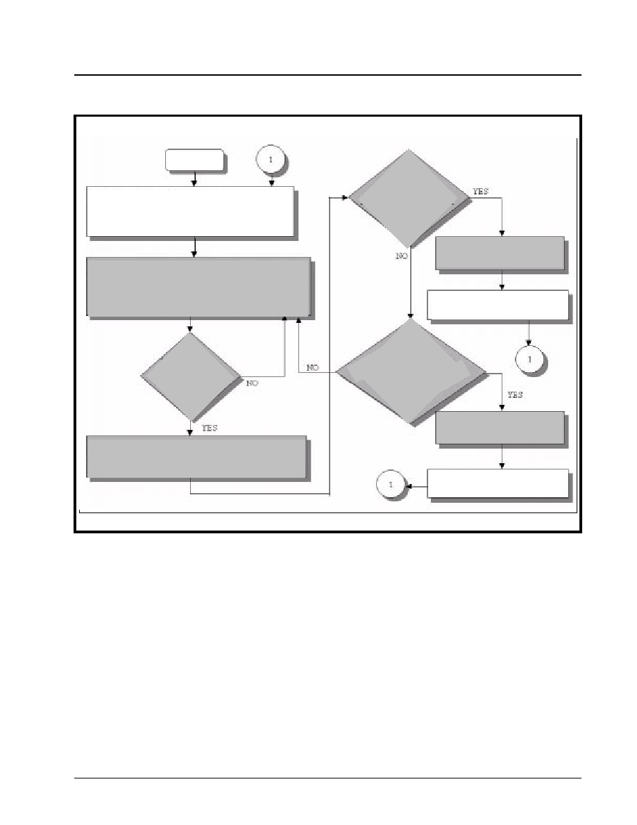
·Á
·Á
·Á
·Á
DS3 UNI FOR ATM
XRT7245
PRELIMINARY
REV. 1.03
231
7.1.2.6
LAPD Receiver
The LAPD Transceiver uses the three "DL" bit fields of
-frame #5, within each M-frame, to transmit and receive
performance monitor data link messages. The "Far-
End" LAPD Transmitter will transmit a LAPD Message
to the "Near-End" Receiver via these three bits within
each DS3 Frame. The LAPD Receiver will receive and
store the information portion of the received LAPD
frame into the "Receive LAPD Message" Buffer,
which is located at addresses: DEh through 135h
within the on-chip RAM. The LAPD Receiver (within
the "Near-End" Receive DS3 Framer) has the follow-
ing responsibilities.
∑
Framing the incoming LAPD Messages
∑
Filtering out stuffed "0s" (within the information
payload)
∑
Storing the Frame Message into the "Receive
LAPD Message" Buffer
∑
Perform Frame Check Sequence (FCS) Verification
∑
Provide status indicators for
≠ End of Message (EOM)
≠ Flag Sequence Byte detected
≠ Abort Sequence detected
≠ Message Type
≠ C/R Type
≠ The occurrence of FCS Errors
The LAPD receiver's actions are facilitated via the
following two registers.
∑
Rx DS3 LAPD Control Register
∑
Rx DS3 LAPD Status Register
F
IGURE
69. F
LOW
D
IAGRAM
DEPICTING
HOW
THE
R
ECEIVE
FEAC P
ROCESSOR
F
UNCTIONS
.
ENABLE THE "FEAC REMOVAL AND
VALIDATION" INTERRUPTS
This is accomplished by writing "xxx 1010" into the
"RxDS3 FEAC Interrupt/Status Register
(Address = 0x13)
RECEIVE FEAC PROCESSOR BEGINS READING IN
THE FEAC BIT-FIELDS (OF INCOMING DS3 FRAMES)
The Receive FEAC Processor checks for the "FEAC
Framing Alignment" pattern of "01111110"
READ IN THE "6-BIT FEAC CODE WORD"
The 6-bit FEAC Code Word immediately follows the
"FEAC Framing Alignment" pattern
GENERATE "FEAC
VALIDATION" INTERRUPT
START
Is the
"FEAC Framing
Alignment" pattern
present in the FEAC
Channel?
INVOKE "FEAC VALIDATION"
INTERRUPT SERVICE ROUTINE
GENERATE "FEAC
REMOVAL" INTERRUPT
INVOKE "FEAC REMOVAL"
INTERRUPT SERVICE ROUTINE
Has this
s a m e F E A C
Code Word been
received in 8 out of the last
10 FEAC message
receptions?
Has a FEAC
Code Word (other than
the last "Validated Code Word)
been received in 3 out of the
last 10 FEAC message
receptions?
XRT7245
DS3 UNI FOR ATM
·Á
·Á
·Á
·Á
PRELIMINARY
REV. 1.03
232
Operation of the LAPD Receiver
The LAPD Receiver, once enabled, will begin searching
for the boundaries of the incoming LAPD message.
The LAPD Message Frame boundaries are
delineated via the "Flag Sequence" octets (7Eh), as
depicted in Table 49.
Where: Flag Sequence = 7Eh
SAPI + CR + EA = 3Ch or 3Eh
TEI + EA = 01h
Control = 03h
The 16 bit FCS is calculated using CRC-16, x
16
+ x
12
+ x
5
+ 1
The local µP (at the "Far End" Terminal), while as-
sembling the LAPD Message frame, will insert an ad-
ditional byte at the beginning of the information (pay-
load) field. This first byte of the information field indi-
cates the type and size of the message being trans-
ferred. The value of this information field and the
corresponding message type/size follow:
CL Path Identification = 38h (76 bytes)
IDLE Signal Identification = 34h (76 bytes)
Test Signal Identification = 32h (76 bytes)
ITU-T Path Identification = 3Fh (82 bytes)
The LAPD Receiver must be enabled before it can
begin receiving any LAPD messages. The LAPD
Receiver can be enabled by writing a "1" to Bit 2
(RxLAPD Enable) of the Rx DS3 LAPD Control Reg-
ister. The bit format of this register is depicted below.
Once the LAPD Receiver has been enabled, it will
begin searching for the Flag Sequence octets (7Eh),
in the "DL" bit-fields, within the incoming DS3 frames.
When the LAPD Receiver finds the flag sequence
byte, it will assert the "Flag Present" bit (Bit 0) within
the Rx DS3 LAPD Status Register, as depicted below.
The receipt of the Flag Sequence octet can mean
one of two things.
1.
The Flag Sequence byte marks the beginning of
an incoming LAPD Message.
T
ABLE
49: LAPD M
ESSAGE
F
RAME
F
ORMAT
F
LAG
S
EQUENCE
(8
BITS
)
SAPI (6-bits)
C/R
EA
TEI (7 bits)
EA
Control (8 bits)
76 or 82 Bytes of Information (Payload)
FCS--MSB
FCS--LSB
Flag Sequence (8 bits)
Rx DS3 LAPD Control Register (Address = 14h)
B
IT
7
B
IT
6
B
IT
5
B
IT
4
B
IT
3
B
IT
2
B
IT
1
B
IT
0
Enable5F(4)
Enable5F(3)
Enable5 F(2)
Enable5 F(1)
Enable5 F(0)
RxLAPD
Enable
RxLAPD
Interrupt
Enable
RxLAPD
Interrupt
Status
R/W
R/W
R/W
R/W
R/W
R/W
R/W
RUR
Rx DS3 LAPD Status Register (Address = 15h)
B
IT
7
B
IT
6
B
IT
5
B
IT
4
B
IT
3
B
IT
2
B
IT
1
B
IT
0
Unused
RxAbort
RxLAPD
Type[0]
RxLAPD
Type[1]
RxCR Type
RxFCS
Error
End Of
Message
Flag
Present
x
x
x
x
x
x
x
1

·Á
·Á
·Á
·Á
DS3 UNI FOR ATM
XRT7245
PRELIMINARY
REV. 1.03
233
2.
The received Flag Sequence octet could be just
one of many Flag Sequence octets that are
transmitted via the DS3 Transport Medium, dur-
ing idle periods between the transmission of
LAPD Messages.
The LAPD Receiver will negate the "Flag Present" bit
as soon as it has received an octet that is something
other than the "Flag Sequence" octet. At this point,
the LAPD Receiver should be receiving either octet #2
of the incoming LAPD Message, or an Abort Sequence
(e.g., a string of seven or more consecutive "1s"). If
this next set of data is an abort sequence, then the
LAPD Receiver will assert the RxAbort bit (Bit 6) of
the Rx DS3 LAPD Status Register. However, if this
next octet is Octet #2 of an incoming LAPD Message,
then the Rx DS3 LAPD Status Register will begin to
present some additional status information on this
incoming message. Each of these indicators are
presented below in sequential order.
Bit 3--RxCR Type--C/R (Command/Response)
Type
This bit-field reflects the contents of the C/R bit-field
within octet #2 of the LAPD Frame Header. When
this bit is "0" it means that this message is originating
from a customer installation. When this bit is "1" it
means that this message is originating from a net-
work terminal.
Bit 4, 5--RxLAPD Type[1, 0]--LAPD Message Type
The combination of these two bit fields indicate the
Message Type and the Message Size of the incoming
LAPD Message frame. The following table relates the
values of Bits 4 and 5 to the Incoming LAPD Message
Type/Size.
Note: The Message Size pertains to the size of the "Infor-
mation portion" of the LAPD Message Frame (as presented
in Table 49).
Bit 3--Flag Present
The LAPD Receiver should receive another "Flag
Sequence" octet, which marks the End of the Message.
Therefore, this bit field should be asserted once again.
Bit 1--EndOfMessage--End of LAPD Message
Frame
Upon receipt of the closing "Flag Sequence" octet,
this bit-field should be asserted. The assertion of this
bit-field indicates that a LAPD Message Frame has
been completely received. Additionally, if this newly
received LAPD Message is different from the previous
message, then the LAPD Receiver will inform the local
µC/µP of the "EndOfMessage" event by generating
an interrupt.
Bit 2--RxFCSErr--Frame Check Sequence Error
Indicator
The LAPD Receiver will take the incoming LAPD
Message and compute its own version of the Frame
Check Sequence (FCS) word. Afterwards, the LAPD
Receiver will compare its computed value with that it
has received from the "Far-End" Transmitter. If these
two values match, then the LAPD Receiver will
presume that the LAPD Message has been properly
received; and the contents of the Received LAPD
Message (payload portion) will be retained at loca-
tions DEh through 135h in on-chip RAM. The LAPD
Receiver will indicate an "error-free" reception of the
LAPD Message by keeping this bit field negated
(Bit 2 = 0). However, if these two FCS values do not
match, then the received LAPD Message is corrupted;
and the user is advised not to process this erroneous
information. The LAPD Receiver will indicate errored
receipt of this message by setting this bit-field to "1".
Note: The Receive DS3 Framer will not generate an inter-
rupt to the local µP, due to the detection of an FCS error.
Therefore, the user is advised to "validate" each and every
received LAPD message by checking this bit-field prior to
processing the LAPD message.
Removal of Stuff Bits from the Payload Portion
of the incoming LAPD Message
While the LAPD Receiver is receiving a LAPD Message,
it has the responsibility of removing all of the "0" stuff
bits from the Payload Portion of the incoming LAPD
T
ABLE
50: T
HE
R
ELATIONSHIP
BETWEEN
R
X
LAPDT
YPE
[1:0]
AND
THE
RESULTING
LAPD M
ESSAGE
TYPE
AND
SIZE
.
R
X
LAPD T
YPE
[1, 0]
M
ESSAGE
T
YPE
M
ESSAGE
S
IZE
00
Test Signal Identification
76 bytes
01
Idle Signal Identification
76 bytes
10
CL Path Identification
76 bytes
11
ITU-T Path Identification
82 bytes
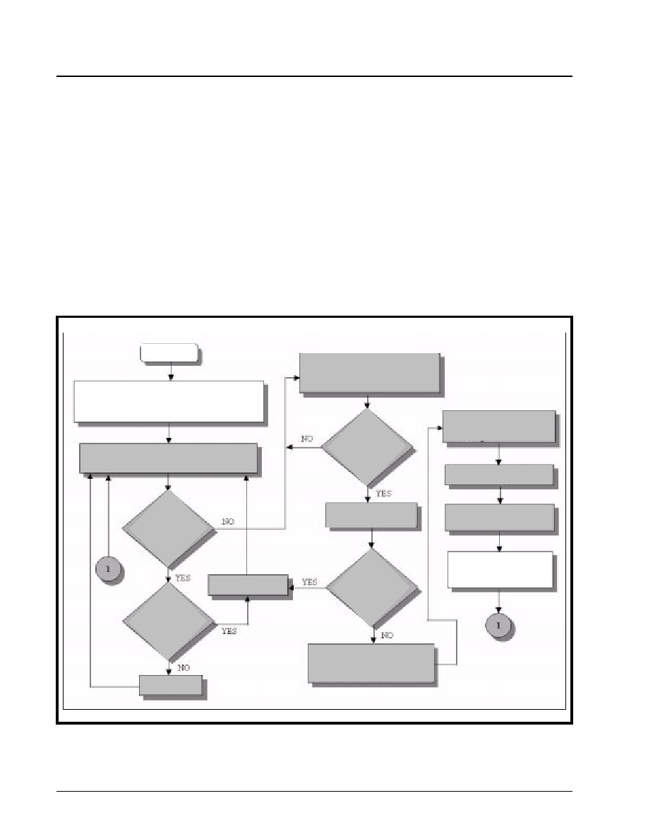
XRT7245
DS3 UNI FOR ATM
·Á
·Á
·Á
·Á
PRELIMINARY
REV. 1.03
234
Message Frame. Recall that the text in Section
6.4.3.1.3 indicated that the LAPD Transmitter (at the
Far-End Transmit DS3 Framer) will insert a "0" imme-
diately following a string of 5 consecutive "1s" within
the payload portion of the LAPD Message frame. The
LAPD Transmitter performs this bit-stuffing procedure
in order to prevent the user data from mimicking the
Flag Sequence octet (7Eh). Therefore, in order to re-
cover the user data to its original form (prior to the
bit-stuffing), the LAPD Receiver will remove the "0"
that immediately follows a string of 5 consecutive "1s".
Writing the Incoming LAPD Message to the
"Receive LAPD Message" Buffer
The LAPD receiver will obtain the LAPD Message
frame from the incoming DS3 data-stream, in addition
to processing the framing overhead octets, perform-
ing error checking (via FCS) and removing the stuffed
"0s" from the user payload data. The LAPD Receiver
will write the payload portion of the LAPD Frame into
the "Receive LAPD Message" buffer at locations DEh
through 135h in on-chip RAM.
Therefore, the local µP/µC must read this location
when it wishes to process this newly received LAPD
Message.
Figure 70 presents a flow chart depicting how the
LAPD Receiver works.
7.1.2.7
FEBE (Far-End-Block Error) Bit-fields
Whenever the Receive DS3 Framer detects P-bit
errors, or is in an "OOF" condition, it will inform the
"Near-End" Transmit DS3 Framer of this fact. The
"Near-End" Transmit DS3 Framer will, in turn, notify
the "Far End" Terminal (e.g., the source of the errored
F
IGURE
70. F
LOW
C
HART
DEPICTING
THE
F
UNCTIONALITY
OF
THE
LAPD R
ECEIVER
ENABLE THE LAPD RECEIVER
This is done by winning the value "0xFC" into the
RxLAPD Control Register (Address = 0x14)
START
LAPD receiver begins reading in the DL bits
from each inbound DS3 frame
D o e s
t h e L A P D
receiver detect 6
consecutive
zeros?
D o e s
t h e L A P D
receiver detect 7
consecutive
zeros?
F l a g S e q u e n c e
A b o r t S e q u e n c e
LAPD receiver is reading in a LAPD
M e s s a g e F r a m e , c o n t a i n i n g a P M D L
M e s s a g e
D o e s
t h e L A P D
receiver detect 6
consecutive
zeros?
D o e s
t h e L A P D
receiver detect 7
consecutive
zeros?
E n d o f M e s s a g e ( E O M )
W r i t e r e c e i v e d P M D L m e s s a g e
into the Receive LAPD Message
Buffer (Address 0xDE - 0x135)
VERIFY THE FCS VALUE
Report results in the RxLAPD
Status Register
"Un-stuff contents of
received message"
Generate "received LAPD
interrupt"
E x e c u t e R e c e i v e L A P D
Interrupt Service Routine
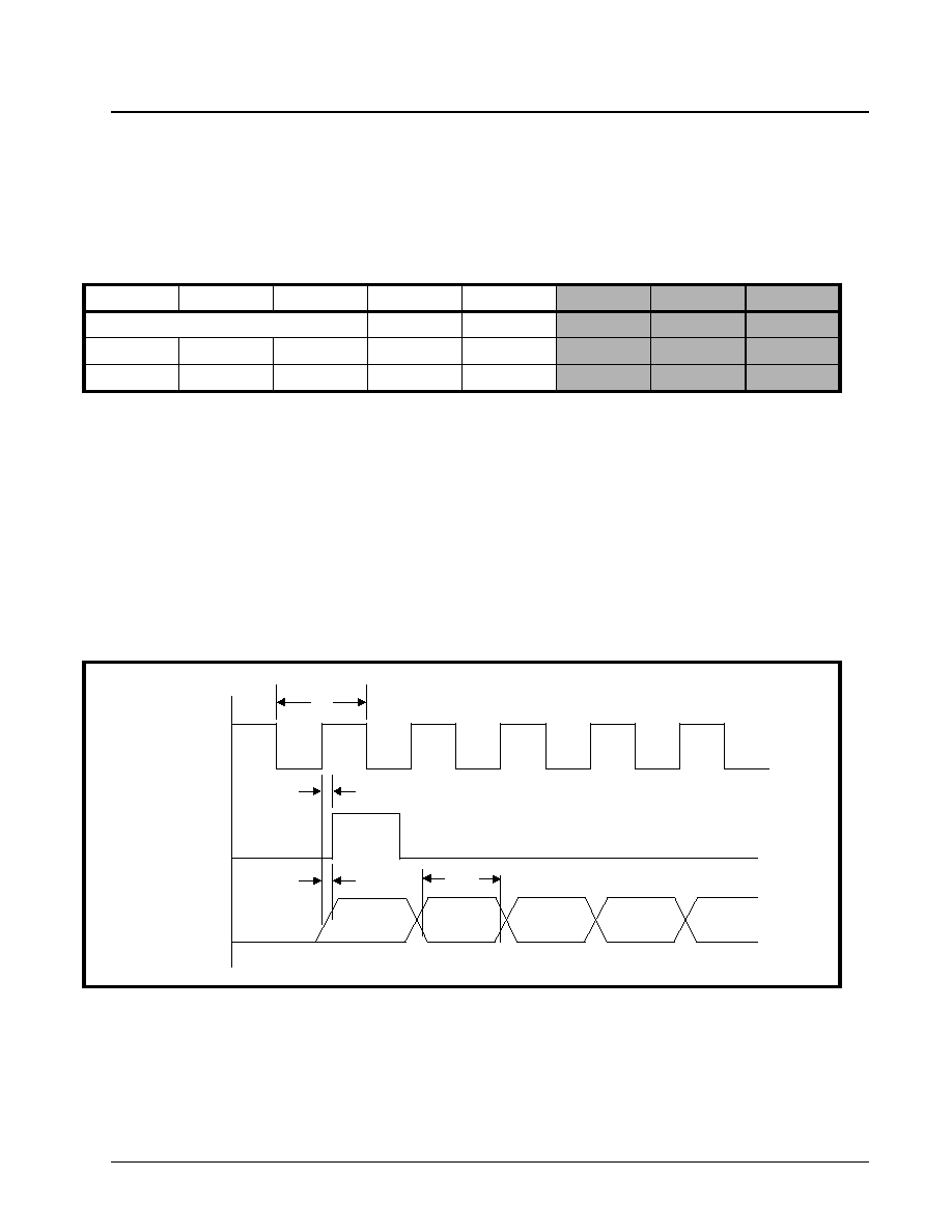
·Á
·Á
·Á
·Á
DS3 UNI FOR ATM
XRT7245
PRELIMINARY
REV. 1.03
235
DS3 data) by transmitting a FEBE pattern of a value
other than `111', out to the "Far End" Terminal.
If the Receive DS3 Framer receives any DS3 frames
containing a FEBE value of some pattern other than
`111' then it will increment the PMON FEBE Event
Count Register--MSB/LSB, which is located at 26h
and 27h in the UNI Address space.
The user can determine the three-bit FEBE pattern,
of the most recently received DS3 Frame by reading
Bit-fields 2 through 0 within the Rx DS3 Status
Register as depicted below.
7.1.2.8
Extracting the DS3 Overhead Bits
via the Serial Output Port
The Receive DS3 Framer block also consists of the
"RxOH" Serial Output port. This serial output port
consists of the following output pins:
∑
RxOH
∑
RxOHClk
∑ RxOHFrame
The Receive DS3 Framer will serially output the OH bits
(of the incoming DS3 Frame) via the "RxOH" output
pin. This output signal will be updated on the rising
edge of the RxOHClk clock signal. Finally, the RxO-
HFrame output pin will pulse "high" when the first
X-bit within a DS3 M-frame is being output at the
RxOH output pin. The order, in which these OH bits
are output (via the RxOH pin) is in accordance with
that in Tables 27 and 28.
Figure 71 presents a timing diagram that illustrates
the behavior of the RxOH Serial Output Port signals.
7.1.2.9
Receive DS3 Framer Interrupt
Conditions
The Receive DS3 Framer can generate an interrupt
request upon any of the following conditions:
∑
Receive Alarms
≠ (e.g., change of state on Receive LOS, OOF,
AIS, Idle detection
≠ Change of state on Receiver FERF, AIC
≠ Detection of Parity Errors in a DS3 Frame
∑
Receive FEAC Processor Interrupt
≠ Validation and removal of receive FEAC code
∑
LAPD Receiver Interrupt
≠ Receipt of a new LAPD message into on-chip
RAM
Address = 0Fh, RxDS3 Status Register
B
IT
7
B
IT
6
B
IT
5
B
IT
4
B
IT
3
B
IT
2
B
IT
1
B
IT
0
Unused
RxFERF
RxAIC
RxFEBE [2]
RxFEBE [1]
RxFEBE [0]
RO
RO
RO
RO
RO
RO
RO
RO
0
0
0
0
0
0
0
0
F
IGURE
71. I
LLUSTRATION
OF
THE
R
X
OH S
ERIAL
O
UTPUT
P
ORT
S
IGNALS
RxOHFrame
RxOHClk
RxOH
t35
t36
t37
t34
F1
X1
F1
AIC
F0
XRT7245
DS3 UNI FOR ATM
·Á
·Á
·Á
·Á
PRELIMINARY
REV. 1.03
236
If one of these conditions occurs, and if that particu-
lar condition is enabled for interrupt generation, then
when the local
µ
P/
µ
C reads the UNI Interrupt Status
Register, as shown below; it should read "1xxxxxxxb"
(where the -b suffix denotes a binary expression, and
the "x" denotes a "don't care" value.)
At this point, the local µC/µP will have determined
that the Receive DS3 Framer block is the source of
the interrupt, and that the Interrupt Service Routine
should branch accordingly. In order to accomplish
this the local µP/µC should now proceed to read one
or all of the following registers.
∑
Rx DS3 Interrupt Status Register (Address = 11h)
∑
Rx DS3 FEAC Interrupt Enable/Status Register
(Address = 13h)
∑ Rx DS3 LAPD Control Register (Address = 14h)
The roles of the bits, within each of these registers to
interrupt processing, are described below.
7.1.2.9.1
Receiver Alarm Related Interrupts
The Receive DS3 Framer will generate an interrupt
request, when the following conditions occur.
∑
Change of State on Receive LOS, OOF, AIS, Idle
Detection
∑
Change of State on Receive FERF, AIC
∑ Detection of Parity Error in a DS3 Frame
Interrupt Servicing of each of these "Receiver-Alarm"
conditions are supported by the Rx DS3 Interrupt
Status Register, which is described below.
Rx DS3 Interrupt Status Register
The bit-format of the Rx DS3 Interrupt Status Register
will flag up to seven different causes of the interrupt.
Associated with the Rx DS3 Interrupt Status Register
is the Rx DS3 Interrupt Enable Register (Address
=10h). The user can write to the Rx DS3 Interrupt
Enable Register in order to disable/enable these indi-
vidual causes of interrupt generation. The bit format
of the Rx DS3 Interrupt Status Register is presented
below.
Bit 0--Parity (P-Bit) Error Interrupt Status
The Receive DS3 Framer asserts this bit if a parity
(P-bit) error is detected in an incoming DS3 Frame. This
bit-field is reset upon being read by the local µC/µP.
Bit 1--Change in OOF Status" Interrupt Status
A "1" in this bit-field indicates that the OOF (Out-of-
Frame) Status has changed since the last time this
register was read. This bit-field is reset upon read.
Note: the Receive DS3 Framer will assert this bit if:
1.
The Receive DS3 Framer loses synchronization
and has declared itself "OOF", or if
2.
The Receive DS3 Framer acquires synchroniza-
tion and has declared itself "In-Frame".
Bit 2--AIC Interrupt Status (C-Bit Parity Mode Only)
A "1" in this bit-field indicates that validated "AIC" has
changed since the last time this register was read.
This bit-field is reset upon read.
UNI Interrupt Status Register (Address = 05h)
B
IT
7
B
IT
6
B
IT
5
B
IT
4
B
IT
3
B
IT
2
B
IT
1
B
IT
0
RxDS3
Interrupt
Status
RxPLCP
Interrupt
Status
RxCP
Interrupt
Status
Rx UTOPIA
Interrupt
Status
Tx UTOPIA
Interrupt
Status
TxCP
Interrupt
Status
TxDS3
Interrupt
Status
One Sec
Interrupt
Status
RO
RO
RO
RO
RO
RO
RO
RUR
Rx DS3 Interrupt Status Register (Address = 11h)
B
IT
7
B
IT
6
B
IT
5
B
IT
4
B
IT
3
B
IT
2
B
IT
1
B
IT
0
Unused
LOS
Interrupt
Status
AIS
Interrupt
Status
IDLE
Interrupt
Status
FERF
Interrupt
Status
AIC
Interrupt
Status
OOF
Interrupt
Status
Parity Error
Interrupt
Status
RO
RUR
RUR
RUR
RUR
RUR
RUR
RUR

·Á
·Á
·Á
·Á
DS3 UNI FOR ATM
XRT7245
PRELIMINARY
REV. 1.03
237
Bit 3--FERF (Far-End Receive Failure) Interrupt
Status
A "1" in this bit-field indicates that the FERF status
has changed since the last time this register bit was
read. In other words, this bit field will be asserted if:
1.
The Receive DS3 Framer begins to detect the
"Yellow Alarm" (e.g., X bits of the incoming DS3
frame are set to 0).
2.
The Receive DS3 Framer ceases in detecting the
"Yellow Alarm) (e.g., X bits has returned to "1").
This bit-field is reset upon read.
Bit 4--"Change in IDLE Status" Interrupt Status
A "1" in this bit-field indicates that the Idle status has
changed since the last time this register bit was read.
Therefore, this bit-field will be asserted if:
1.
The Receiver DS3 Framer just declares the "Idle"
condition
2.
The Receiver DS3 Framer has just negated the
"Idle" condition.
Bit 5--"Change in AIS Status" Interrupt Status
A "1" in this bit field indicates that the AIS-Status of
the Receive DS3 Framer has changed since the last
time this register bit was read. Therefore, the Receive
DS3 Framer will set this bit when:
1.
The Receive DS3 Framer declares an "AIS
Condition" or
2.
The Receive DS3 Framer terminates the declara-
tion of an "AIS Condition".
Bit 6--"Change in LOS (Loss of Signal) Status"
Interrupt Status
A "1" in this bit-field indicates that the "LOS-Status" of
the Receive DS3 Framer has changed since the last
time register bit was read. Therefore, the Receive
DS3 Framer will set this bit when:
1.
The Receive DS3 Framer declares an "LOS
Condition" or,
2.
The Receive DS3 Framer terminates the declara-
tion of an "LOS Condition".
The Rx DS3 Interrupt Status Register is associated
with the Receive DS3 Interrupt Enable Register,
which has the exact same bit-format; and is used to
enable/disable each of these interrupt conditions. The
bit-format of the Rx DS3 Interrupt Enable Register is
presented below.
The user can enable a given interrupt condition by
writing a "1" to the corresponding bit-field. Likewise,
the user can disable a given interrupt condition by,
instead writing a "0" to that bit-field.
7.1.2.9.2
The Receive FEAC Processor
Interrupts
The Receive FEAC Processor will generate an
interrupt request under the following conditions.
∑
Validation of an incoming FEAC Code
∑ Removal of a previously validated FEAC Code
The servicing of interrupts associated with the
Receive FEAC Processor are supported by the Rx DS3
FEAC Interrupt Enable/Status Register. The features
associated with this register are presented below.
Rx DS3 FEAC Interrupt Enable/Status Register
The bit format of this register is presented below.
Rx DS3 Interrupt Enable Register (Address = 10h)
B
IT
7
B
IT
6
B
IT
5
B
IT
4
B
IT
3
B
IT
2
B
IT
1
B
IT
0
Unused
LOS
Interrupt
Enable
AIS
Interrupt
Enable
IDLE
Interrupt
Enable
FERF
Interrupt
Enable
AIC
Interrupt
Enable
OOF
Interrupt
Enable
Parity Error
Interrupt
Enable
RO
R/W
R/W
R/W
R/W
R/W
R/W
R/W
XRT7245
DS3 UNI FOR ATM
·Á
·Á
·Á
·Á
PRELIMINARY
REV. 1.03
238
The Rx DS3 FEAC Interrupt Enable/Status Register
consists of 5 active bit-fields. However, only 4 of
these bit fields are relevant to interrupt processing.
Bit 0--Rx FEAC Valid Interrupt Status
A "1" in this bit-field indicates that a newly received
FEAC Message has been validated by the Receive
FEAC Processor. The Receive FEAC Processor will
validate a FEAC Message if both of the following
conditions are met.
1.
The same message has been received during 8
out of the last 10 transmission from the Far End
Transmitter, and
2.
This new, incoming FEAC Message is different
from the previous validated FEAC message.
Bit 1--Rx FEAC Valid Interrupt Enable
This bit allows the user to enable/disable the "Rx FEAC
Valid" Interrupt. Writing a "1" to this bit-field enables
this interrupt. Whereas, writing a "0" disables this in-
terrupt. The value of this bit field is "0" following
power up or reset.
Bit 2--Rx FEAC Removal Interrupt Status
A "1" in this bit-field indicates that the last "validated"
FEAC Message has now been removed by the
Receive FEAC Processor. The Receive FEAC
Processor will remove a validated FEAC message if
3 out of the last 10 received FEAC messages differ
from this valid FEAC message.
Bit 3--Rx FEAC Removal Interrupt Enable
This bit field allows the user to enable/disable the "Rx
FEAC Removal" interrupt. Writing a "1" to this bit
enables this interrupt. Likewise, writing a "0" to this
bit-field disables this interrupt.
7.1.2.9.3
LAPD Receiver Interrupts
The LAPD Receiver also has the ability to generate
an interrupt to the µC/µP, when it (the LAPD Receiver)
has finished receiving an incoming LAPD message.
The purpose of this interrupt is to inform the µC/µP
that there is a newly received LAPD message that is
ready to be read by the µC/µP. Interrupt servicing of
this type of interrupt is supported via the Rx DS3
LAPD Status Register. The features associated with
this register are described below.
Rx DS3 LAPD Control Register
The Rx DS3 LAPD Control register consists of 8 active
bit-fields. However, only 2 of these 8 are related to
servicing the LAPD Receiver-related interrupts. The
bit format of this register is presented below.
Bit 0--RxLAPD Interrupt Status
A "1" in this bit-field indicates that the LAPD Receiver
has received a full-LAPD message frame, and that
the information portion of this LAPD frame is available
in the "Receive LAPD Message" buffer for reading by
the local µC/µP.
Note: This interrupt does not indicate that this new LAPD
Message is valid or "error-free". The user is advised to ver-
ify that error-free reception occurred, by reading Bit 2 of the
Rx DS3 LAPD Status Register.
Rx DS3 FEAC Interrupt Enable/Status Register (Address = 13h)
B
IT
7
B
IT
6
B
IT
5
B
IT
4
B
IT
3
B
IT
2
B
IT
1
B
IT
0
Unused
Unused
Unused
FEAC
Valid
RxFEAC Remove
Interrupt Enable
RxFEAC
Remove
Interrupt Status
RxFEAC Valid
Interrupt
Enable
RxFEAC Valid
Interrupt
Status
R/O
R/O
R/O
R/O
R/W
RUR
R/W
RUR
Rx DS3 LAPD Control Register (Address = 14h)
B
IT
7
B
IT
6
B
IT
5
B
IT
4
B
IT
3
B
IT
2
B
IT
1
B
IT
0
Enable5
F(4)
Enable5
F(3)
Enable5
F(2)
Enable5
F(1)
Enable5
F(0)
RxLAPD
Enable
RxLAPD Interrupt
Enable
RxLAPD Interrupt
Status
R/W
R/W
R/W
R/W
R/W
R/W
R/W
RUR
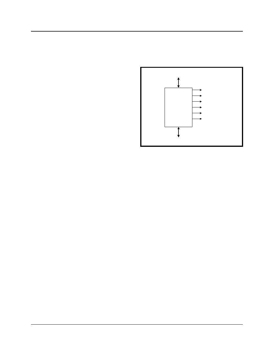
·Á
·Á
·Á
·Á
DS3 UNI FOR ATM
XRT7245
PRELIMINARY
REV. 1.03
239
Bit 1--RxLAPD Interrupt Enable
This bit-field allows the user to enable/disable the
"RxLAPD Interrupt". Writing a "1" to this bit-field
enables this interrupt. Whereas, writing a "0" disables
this interrupt. The value of this bit-field is "0" following
power up or reset.
7.2
Receive PLCP Processor
7.2.1
Operation of the Receive PLCP Processor
The Receive PLCP Processor receives PLCP frame
data from the Receive DS3 Framer and locates the
boundaries of these incoming PLCP frames. The
Receive PLCP processor also extracts the PLCP
overhead bytes, computes and verifies the incoming
BIP-8 (B1) byte, transfers FEBE and Yellow Alarm
information to the "Near-End" Transmit PLCP
Processor, for transmittal back to the Far-End Terminal.
Finally, these PLCP frames (and their designated
boundaries) are routed to the Receive Cell Processor,
for further processing.
Note: The Receive PLCP Processor is disabled when the
UNI is operating in the "Direct Mapped ATM" mode.
Figure 72 presents a simple illustration of the Receive
PLCP Processor block along with the associated
external pins.
7.2.2
Functional Description of the Receive
PLCP Processor
The Receive PLCP Processor receives and operates
on data extracted from the payload-portion of the
incoming DS3 data stream (via the Receive DS3
Framer). Once the Receive DS3 Framer reaches the
"In-Frame" state, then the Receive PLCP Processor
will take this incoming data and begin searching for
the PLCP frame boundaries. The Receive PLCP
Processor will inform the "outside world" that it has
began detecting these PLCP frame boundaries by
pulsing the RxPFrame output pin. Figure 73, presents
a Functional Block Diagram of the Receive PLCP
Processor and Table 51 presents the Byte Format for
a PLCP Frame.
F
IGURE
72. I
LLUSTRATION
OF
THE
S
IMPLE
B
LOCK
D
IAGRAM
OF
THE
R
ECEIVE
PLCP P
ROCESSOR
To Rx Framer
To Rx Cell Processor
RxPOHClk
RxPOHFrame
RxPOH
RxPFrame
RxPLOF
RxPOOF
Receive PLCP
Processor
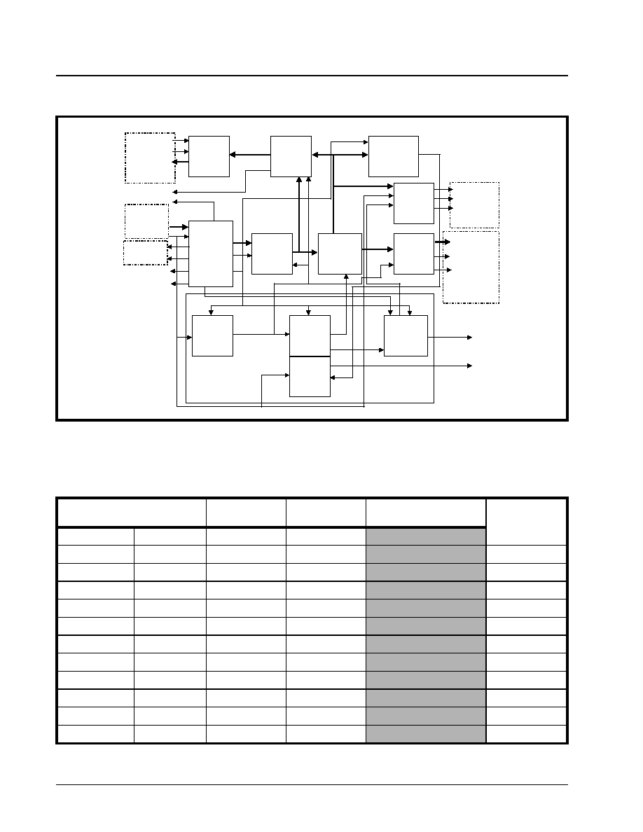
XRT7245
DS3 UNI FOR ATM
·Á
·Á
·Á
·Á
PRELIMINARY
REV. 1.03
240
Figure 73 indicates that the PLCP Frame consists of
12 ATM Cells, 48 bytes of Overhead (OH) bytes, and
13 or 14 nibbles of "trailer" for frequency justification.
F
IGURE
73. F
UNCTIONAL
B
LOCK
D
IAGRAM
OF
THE
R
ECEIVE
PLCP P
ROCESSOR
B
LOCK
FEBE
Bucket
BIP
Calculator
&
Comparator
C1 Byte
Stuff
Decoder
(Majority Logic)
Over Head
Extractor
to
Serial Port
Cell Data
Extractor
Pay Load
Over Head
DeMUX
Nibble/Byte
Converter
Frame
Synchronizer
Byte
Clock
Generator
(Divide by 2)
Column
Counter
(Divide by 57)
Stuff
Counter
(Divide by
13/14)
Row
Counter
(Divide by 12)
TxPFrame
TxFEBE RdClk
RxFEBE
To PMON
BIP-8 Errors
FA Byte Errors
OOF
OOF
OOF/LOF
C1 Byte
B1 Byte
CellData
RxPOH
RxPOHClk
RxPOHFrame
RxCellData
RxCellClock
RxNbDat
RxNbClk
RxPLOF
RxPOOF
OOF Interrupt
LOF Interrupt
Overhead Data
NibbleClk
ByteData
RxNbClk
Byte Clock
RxCellClockEnable
RxPFrame
RxPStuff
To
TxPLCP
Framer
Column Clock
C1 Byte
Control
Timing & Control
Byte
Clock
To Rx Cell
Processor
To Pins
From RxDS3
Framer
To/From
TxPLCP Framer
T
ABLE
51: B
YTE
F
ORMAT
OF
THE
PLCP F
RAME
PLCP F
RAME
2
BYTES
POI
1
BYTE
POH
1
BYTE
PLCP P
AYLOAD
53
BYTES
13-14
NIBBLES
A1
A2
P11
Z6
First ATM Cell
A1
A2
P10
Z5
ATM Cell
A1
A2
P9
Z4
ATM Cell
A1
A2
P8
Z3
ATM Cell
A1
A2
P7
Z2
ATM Cell
A1
A2
P6
Z1
ATM Cell
A1
A2
P5
X
ATM Cell
A1
A2
P4
B1
ATM Cell
A1
A2
P3
G1
ATM Cell
A1
A2
P2
X
ATM Cell
A1
A2
P1
X
ATM Cell
A1
A2
P0
C1
Twelfth ATM Cell
Trailer
·Á
·Á
·Á
·Á
DS3 UNI FOR ATM
XRT7245
PRELIMINARY
REV. 1.03
241
The contents of the Path Overhead (POH) bytes
(e.g., Z6 through C1) of the incoming PLCP frame
is output via a serial port consisting of the RxPOH,
RxPOHClk, and RxPOHFrame output pins. This
serial output port is discussed in greater detail in
section 7.2.2.3.
7.2.2.1
PLCP Framing
At any given time, the Receive PLCP Processor will
be operating in any one of three (3) "framing" modes.
∑
Un-Framed
∑
Out-of-Frame (OOF)
∑ In-Frame
The State Machine diagram of the Receive PLCP
Processor framing algorithm is presented in Figure 74,
and each of these framing modes are discussed.
7.2.2.1.1
The Un-Framed Mode
When the Receive PLCP processor is operating in
the "Un-Framed" mode, it does not have any form of
frame synchronization with the incoming PLCP data.
The Receive PLCP Processor will indicate that it is in
the "Un-Framed" Mode to external circuitry by assert-
ing both the RxPOOF and RxPLOF output pins and
the "POOF Status" and "PLOF Status" bits within the
Rx PLCP Configuration/Status Register, as depicted
below.
The Receive PLCP Processor will attempt to acquire
PLCP framing once the Receive DS3 Framer has
reached the "In-Frame" state. Specifically, the
Receive PLCP Processor will attempt to find the
F
IGURE
74. S
TATE
M
ACHINE
D
IAGRAM
OF
THE
R
ECEIVE
PLCP P
ROCESSOR
F
RAMING
A
LGORITHM
Un-Framed
Mode
Out-of-Frame
Mode
In-Frame
Mode
2 Consecutive sets of A1, A2, and POI
bytes are correct, and the recovered POIs
are in the correct sequence.
Errors are detected in two
consecutive framing bytes
(A1, A2) or 2 consecutive
POIs are incorrect.
2 Consecutive sets of A1, A2, and POI
bytes are correct, and the recovered POIs
are in the correct sequence.
T h e O O F
condition
persists for
more than
1ms.
Rx PLCP Configuration/Status Register (Address = 44h)
B
IT
7
B
IT
6
B
IT
5
B
IT
4
B
IT
3
B
IT
2
B
IT
1
B
IT
0
Unused
Reframe
POOF Status
PLOF Status
Yellow Status
x
x
x
x
x
1
1
x
XRT7245
DS3 UNI FOR ATM
·Á
·Á
·Á
·Á
PRELIMINARY
REV. 1.03
242
boundaries of the PLCP frames by first searching for
the Frame Alignment bytes: A1 and A2. The value of
the A1 and A2 bytes are F6h and 28h, respectively.
After the Receive PLCP Processor locates the Frame
Alignment bytes, it will then begin to read and align
itself in accordance with the POI (Path Overhead
Indicator) bytes.
The Receive PLCP processor will declare itself "in-
frame" if two consecutive sets of A1, A2 and POI bytes
are correct and if the received POIs are in the correct
sequence.
7.2.2.1.2
In-Frame (Frame Maintenance Mode)
When the Receive PLCP Processor is operating in
the "In-Frame" mode, it means that it is continually
correctly locating the boundaries of the incoming
PLCP frames. This also enables the Receive PLCP
Processor to perform its tasks of POH byte extraction
and processing. The Receive PLCP processor will in-
dicate its detection of a PLCP frame boundary by
pulsing the RxPFrame output pin "high" at the end of
each frame. Therefore, the pulse rate of this output
pin is nominally 8 kHz. The Receive PLCP Processor
will notify the localµC/µP of its transition from the
"Un-framed" to the "In-frame" state by:
1.
Negating both the RxPOOF and RxPLOF output
pins
2.
Negating both the POOF Status and PLOF
Status bits in the Rx PLCP Configuration/Status
Register.
3.
Generating a "Change of OOF/LOF" status
interrupt request to the local µC/µP.
Additionally, while the Receive PLCP Processor is
operating in the "In-frame" mode, it also will be per-
forming "Frame Maintenance" functions by continually
checking for and report framing errors. The user can
monitor the number of Framing Errors that have been
detected by the Receive PLCP Processor by reading
the PMON PLCP Framing Byte Error Count Registers
which are located at Addresses 2Ah and 2Bh. The
bit-formats of these two registers are presented below.
The contents of these registers reflect the total num-
ber of PLCP Framing Errors that have been detected
since the last read of these registers. These registers
are reset upon read.
7.2.2.1.3
Out-of-Frame (OOF) Mode
The Receive PLCP Processor will declare an "Out-of-
Frame" (OOF) condition, if:
∑
Errors are detected in two consecutive framing
bytes (A1, A2), or
∑ Two consecutive POIs values are both incorrect.
Once the Receive PLCP Processor declares "OOF",
then it will enter the "Out-of-Frame" state (per Figure 74).
Please note that this mode should not be confused
with the "Un-Framed" mode.
When the Receive PLCP Processor is operating in
the "OOF" mode, it will attempt to re-acquire the
"In-frame" status. However, the Receive PLCP
Processor will continue to use the previous frame
synchronization, while operating in this mode. If the
Receive PLCP Processor cannot re-acquire the
"In-Frame" status after being in the "OOF" mode for
1ms (approximately 8 PLCP frames) or more, then
the Receive PLCP Processor will declare a "Loss of
Frame" and will transition back to the "Un-Framed
Mode".
Address = 2Ah, PMON PLCP Framing Byte Error Count Register--MSB
B
IT
7
B
IT
6
B
IT
5
B
IT
4
B
IT
3
B
IT
2
B
IT
1
B
IT
0
FA Error Count--High Byte
RO
RO
RO
RO
RO
RO
RO
RO
0
0
0
0
0
0
0
0
Address = 2Bh, PMON PLCP Framing Byte Error Count Register--LSB
B
IT
7
B
IT
6
B
IT
5
B
IT
4
B
IT
3
B
IT
2
B
IT
1
B
IT
0
FA Error Count--Low Byte
RO
RO
RO
RO
RO
RO
RO
RO
0
0
0
0
0
0
0
0
·Á
·Á
·Á
·Á
DS3 UNI FOR ATM
XRT7245
PRELIMINARY
REV. 1.03
243
The Receive PLCP Processor will indicate its transi-
tion to the "Out-of-Frame" mode by
1.
Asserting the RxPOOF pin (Note: the RxPLOF
pin will still remain negated).
2.
Asserting the "POOF" status bit in the Rx PLCP
Configuration/Status Register.
3.
Generating a "Change of OOF" status interrupt
request to the local µC/µP.
If the Receive PLCP Processor is able to regain Frame
Synchronization, it will negate the RxOOF output pin
and "POOF Status" bit-field in the "Rx PLCP Configu-
ration/Status Register. The Receive PLCP Processor
will also alert the local µP/µC of this occurrence by
generating the "Change in OOF Condition" interrupt.
The user can determine the framing state that the
Receive PLCP Processor is operating in by reading
bits 1 and 2 of the Receive PLCP Configuration
Status Register. The bit-format of this register is
presented below.
Bit 1--PLOF Status
A "1" in this bit-field indicates a "Loss of Frame" status.
Consequently, the Receive PLCP Processor will be
operating in the "Un-framed" state. Conversely, a "0"
in this bit-field indicates that the Receive PLCP
Processor is either in the "In-Frame" or "Out-of-
Frame" state.
Note: the state of this bit-field (and the RxLOF output pin)
is controlled by the contents of an Up/Down Counter. This
counter is incremented whenever the "POOF Status" bit is
"1" and is decremented when the "POOF Status bit is `0'.
However, the counter is decremented at 1/12th of the rate
that it is incremented. Therefore, when the Receive PLCP
Processor goes into the "OOF" condition, this Up/Down
Counter will increment. If the Receive PLCP Processor
requires 1ms to regain Frame-Synchronization, the PLOF
bit-field might very well be asserted, denoting an "LOF con-
dition". However, even after the Receive PLCP Processor
has declared itself "In-Frame", the PLOF bit-field will not be
negated until the POOF bit-field has been negated for 12 ms.
Bit 2--POOF Status
A "1" in this bit-field indicates an "Out-of-Frame"
condition. This condition necessarily indicates that
the Receive PLCP Processor is not in the "In-frame"
condition. Therefore, the user will have to read-in the
value of bit 1 in order to determine if the Receive
PLCP Processor is operating in the "Out-of-Frame" or
"Un-Framed" state.
The following table relates the "read-in" values for
bits 1 and 2 to the framing state of the Receive PLCP
Processor.
7.2.2.1.4
Reframe via Software Command
The UNI allows the user to force the Receive PLCP
Processor into the "OOF" mode, via software
command. The user can accomplish this by writing a
"1" to Bit 3 in the Rx PLCP Configuration/Status
Register, as depicted below.
Rx PLCP Configuration/Status Register (Address = 44h)
B
IT
7
B
IT
6
B
IT
5
B
IT
4
B
IT
3
B
IT
2
B
IT
1
B
IT
0
Unused
Reframe
POOF Status
PLOF Status
Yellow Status
RO
RO
RO
RO
R/W
RO
RO
RO
T
ABLE
52: T
HE
R
ELATIONSHIP
BETWEEN
THE
LOGIC
STATES
OF
THE
POOF
AND
PLOF
BIT
-
FIELDS
,
AND
THE
CORRESPONDING
R
ECEIVE
PLCP F
RAMING
S
TATE
POOF B
IT
2
PLOF B
IT
1
R
ECEIVE
PLCP F
RAMING
S
TATE
0
0
In-Frame
0
1
In-Frame--PLOF is still "1" during the "12 ms period" that POOF is "0"
1
0
Out of Frame
1
1
Un-frame
XRT7245
DS3 UNI FOR ATM
·Á
·Á
·Á
·Á
PRELIMINARY
REV. 1.03
244
7.2.2.2
Overhead Byte Processing
Once the Receive PLCP Processor enters into the "In-
frame" mode, the 12 POH bytes are then extracted
and output via a serial output port. Presently, the Re-
ceive PLCP Processor is only concerned with three
(3) of these POH bytes: B1, G1, and C1. The manner
in which the Receive PLCP Processor handles these
POH bytes follows.
7.2.2.2.1
B1 (BIP-8) Byte
The Receive PLCP Processor will perform a BIP-8
calculation over an entire PLCP frame (excluding the
A1, A2 and POI bytes) that it receives from the
Receive DS3 Framer. Afterwards, the Receive PLCP
Processor will read in the B1 byte, of the very next
incoming PLCP frame, and perform a bit-by-bit
comparison between this B1 byte and this locally-
computed BIP-8 value. By the nature of the BIP-8
values, it is possible to have as many as 8 bit errors
in this comparison. If the Receive PLCP Processor
detects any BIP-8 errors, then it will do two things:
∑
increment the PMON BIP-8 Error Count Registers
(Address = 28h and 29h) by the number of
detected bit-errors, and,
∑ Inform the "Far-End" Terminal (e.g., the source of
the errored data) of this occurrence by routing the
number of bit-errors that were detected in this
frame to the "Near-End" Transmit PLCP Processor.
The Transmit PLCP Processor will then insert this
number into the FEBE-nibble within the G1 byte of
an outbound PLCP frame. Then the outbound
PLCP frame (containing the information on the B1
byte error) will be transmitted to the "Far-End" ter-
minal where it will be processed appropriately.
Table 53 presents the bit format of the G1 byte. The
Receive PLCP processor performs this function in
order to inform the "Far-End Terminal that bit errors
have been detected in its transmission.
The bit-format of the PMON BIP-8 Error Count Reg-
ister (Address = 28h and 29h) are presented below.
Rx PLCP Configuration/Status Register (Address = 44h)
B
IT
7
B
IT
6
B
IT
5
B
IT
4
B
IT
3
B
IT
2
B
IT
1
B
IT
0
Unused
Reframe
POOF Status
PLOF Status
Yellow Status
x
x
x
x
1
x
x
x
T
ABLE
53: B
IT
F
ORMAT
OF
THE
G1 B
YTE
B
IT
7
B
IT
6
B
IT
5
B
IT
4
B
IT
3
B
IT
2
B
IT
1
B
IT
0
Far End Block Error (FEBE)
RAI (Yellow)
X bits (Ignored by the Receiver)
4 Bits
1 Bit
3 Bits
Address = 28h, PMON BIP-8 Error Count Register--MSB
B
IT
7
B
IT
6
B
IT
5
B
IT
4
B
IT
3
B
IT
2
B
IT
1
B
IT
0
BIP-8 Error Count--High Byte
RO
RO
RO
RO
RO
RO
RO
RO
0
0
0
0
0
0
0
0
Address = 29h, PMON BIP-8 Error Count Register--LSB
B
IT
7
B
IT
6
B
IT
5
B
IT
4
B
IT
3
B
IT
2
B
IT
1
B
IT
0
BIP-8 Error Count--Low Byte
RO
RO
RO
RO
RO
RO
RO
RO
·Á
·Á
·Á
·Á
DS3 UNI FOR ATM
XRT7245
PRELIMINARY
REV. 1.03
245
The contents of these registers reflect the total num-
ber of BIP-8 Errors that have been detected since the
last read of these registers. These registers are reset
upon read.
7.2.2.2.2
G1 Byte
The incoming G1 Byte serves to provide the "Near-End"
Terminal with diagnostic information on the quality of
the transmission link between the "Near-End" Transmit
PLCP Processor and the "Far-End" Receive PLCP
Processor. The bit-format of the G1 byte, presented
in Figure 69, indicates that 5 of the 8 bits in this byte
are relevant to transmission diagnosis.
Bit 3--RAI--Yellow Alarm Indicator
This bit-field serves as a "Yellow Alarm" indicator.
The "Far-End" Transmit PLCP Processor will assert
this bit-field if the "Far End" Receive PLCP Processor
has had sufficient trouble receiving valid data from
the "Near-End" Transmit PLCP Processor; and that
this condition has persisted for 2 to 10 seconds. If
this bit-field is asserted for 10 consecutive incoming
PLCP frames then the Receive PLCP Processor will
assert the "Yellow Alarm" status bit (Bit 0) within the
Receive PLCP Configuration/Status Register, as
depicted below.
Bit 0, within the Receive PLCP Configuration Status
register will be negated when the Receive PLCP Pro-
cessor has received 10 consecutive G1 bytes with
the RAI bit-field being "0".
Bits 4 through 7--FEBE
This nibble-field represents the number of "BIP-8" bit-
errors that were detected by the "Far-End" Receive
PLCP Processor in a given PLCP frame. Because of
the nature of the BIP-8 value, the FEBE nibble-field
can indicate as many as 8 bit-errors. If the "Near-End"
Receive PLCP Processor receives a G1 byte that
contains a non-zero FEBE value, then the "Near-
End" Receive PLCP Processor will increment the
PMON PLCP FEBE Count Register (Address = 2C,
2D) by the value of the FEAC nibble-field within the
received G1 byte. The bit-format of these registers is
presented below.
0
0
0
0
0
0
0
0
Address = 29h, PMON BIP-8 Error Count Register--LSB
B
IT
7
B
IT
6
B
IT
5
B
IT
4
B
IT
3
B
IT
2
B
IT
1
B
IT
0
Rx PLCP Configuration/Status Register (Address = 44h)
B
IT
7
B
IT
6
B
IT
5
B
IT
4
B
IT
3
B
IT
2
B
IT
1
B
IT
0
Unused
Reframe
POOF Status
PLOF Status
Yellow Status
x
x
x
x
x
x
x
1
Address = 2Ch, PMON PLCP FEBE Count Register--MSB
B
IT
7
B
IT
6
B
IT
5
B
IT
4
B
IT
3
B
IT
2
B
IT
1
B
IT
0
PFEBE Count--High Byte
RO
RO
RO
RO
RO
RO
RO
RO
0
0
0
0
0
0
0
0
Address = 2Dh, PMON PLCP FEBE Count Register--LSB
B
IT
7
B
IT
6
B
IT
5
B
IT
4
B
IT
3
B
IT
2
B
IT
1
B
IT
0
PFEBE Count--Low Byte
RO
RO
RO
RO
RO
RO
RO
RO
0
0
0
0
0
0
0
0
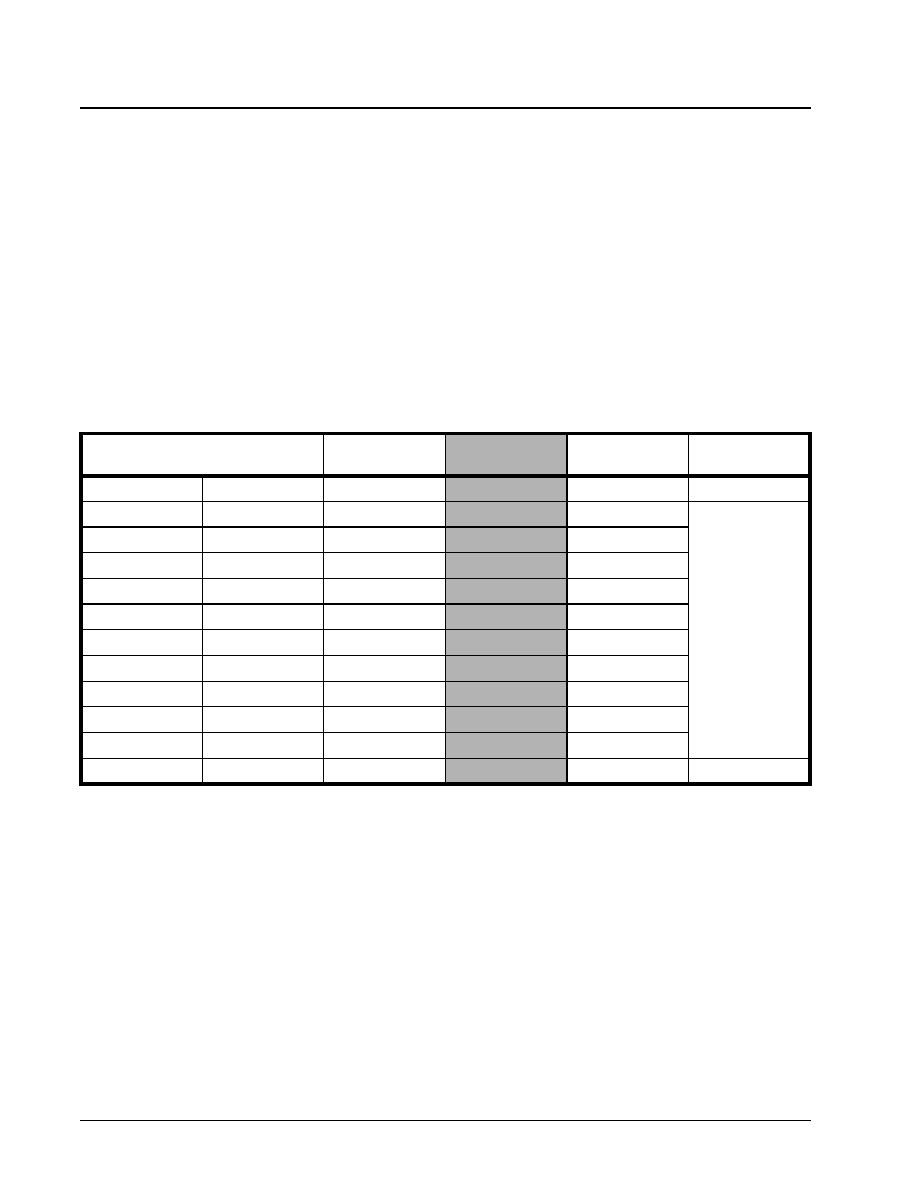
XRT7245
DS3 UNI FOR ATM
·Á
·Á
·Á
·Á
PRELIMINARY
REV. 1.03
246
7.2.2.2.3
C1 Byte
The Receive PLCP processor will determine the
number of trailer nibbles that exist in a given frame by
reading the contents of the incoming C1 byte which is
the POH byte of the 12th row of a PLCP frame. For a
detailed discussion on the meaning of the C1 Byte,
please see Section 6.3.3.1.
7.2.2.3
Extracting PLCP Overhead Bytes via
the Serial Output Port
Once the Receive PLCP Processor declares itself
"In-Frame", then it will begin to output data via the
"Receive PLCP Processor POH Byte" serial output
port. The "Receive PLCP Processor POH Byte" serial
output port consists of the following output pins.
∑
RxPOH
∑
RxPOHFrame
∑ RxPOHClk
Table 54 presents the byte format of the PLCP frame.
The "shaded" bytes represent the data that is output
via the RxPOH pin. Each POH byte is output with the
MSB (most significant bit) first. Each bit, within each
of these POH bytes is output on the rising edge of
the RxPOHClk signal. The RxPOHClk signal has a
nominal frequency of 768 kHz. The Receive PLCP
Processor will assert the RxPOHFrame signal when
the MSB of the Z6 byte is output via the RxPOH out-
put pin.
Figure 75 presents a drawing of waveforms illustrat-
ing the timing relationship between RxPOH, RxPO-
HFrame, and RxPOHClk.
T
ABLE
54: B
YTE
F
ORMAT
OF
PLCP F
RAME
≠POH B
YTES
H
IGHLIGHTED
.
PLCP F
RAME
2 B
YTES
POI
1 B
YTE
POH
1 B
YTE
PLCP P
AYLOAD
53 B
YTES
A1
A2
P11
Z6
First ATM Cell
13≠14 Nibbles
A1
A2
P10
Z5
ATM Cell
A1
A2
P9
Z4
ATM Cell
A1
A2
P8
Z3
ATM Cell
A1
A2
P7
Z2
ATM Cell
A1
A2
P6
Z1
ATM Cell
A1
A2
P5
X
ATM Cell
A1
A2
P4
B1
ATM Cell
A1
A2
P3
G1
ATM Cell
A1
A2
P2
X
ATM Cell
A1
A2
P1
X
ATM Cell
A1
A2
P0
C1
Twelfth ATM Cell
Trailer
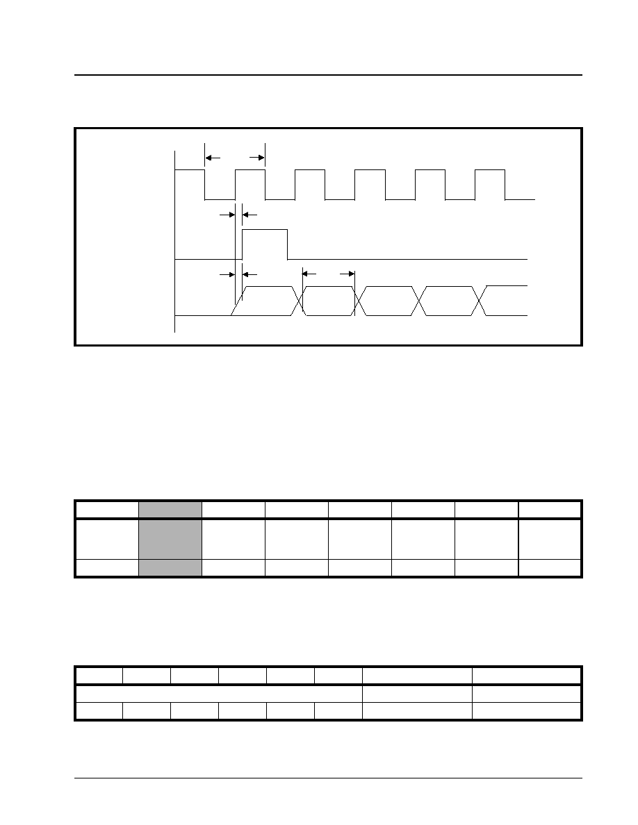
·Á
·Á
·Á
·Á
DS3 UNI FOR ATM
XRT7245
PRELIMINARY
REV. 1.03
247
7.2.2.4
Direct-Mapped ATM Mode
The Receive PLCP Processor will be disabled if the
XRT7245 DS3 UNI is configured to operate in the
"Direct Mapped ATM" Mode.
7.2.2.5
Receive PLCP Processor-related
Interrupts
The Receive PLCP Processor will generate interrupts
upon the following conditions:
∑
Change in OOF status
∑ Change in LOF status
If one of these conditions occur, and if that particular
condition is enabled for interrupt generation, then
when the local
µ
C/
µ
P reads the UNI Interrupt Status
Register, as shown below; it should read "x1xxxxxxb"
(where the -b suffix denotes a binary expression, and
the "x" denotes a "don't care" value).
At this point, the local µC/µP will have determined
that the Receive PLCP Processor block is the source
of the interrupt, and that the Interrupt Service Routine
should branch accordingly. In order to accomplish
this the local µP/µC should now read the Rx PLCP
Interrupt Status Register. The bit-format of the Rx
PLCP Interrupt Status register is presented below.
The bit format of the Rx PLCP Interrupt Status
Register indicates that only two (2) bit-fields, within
this register, are active. The role of each of these bit
fields follows.
F
IGURE
75. T
IMING
R
ELATIONSHIP
BETWEEN
THE
R
ECEIVE
PLCP POH B
YTE
S
ERIAL
O
UTPUT
P
ORT
PINS
--R
X
POH,
R
X
POHF
RAME
AND
R
X
POHC
LK
.
RxPOHFrame
RxPOHClk
RxPOH
t44
t45
t46
t43
UNI Interrupt Status Register (Address = 05h)
B
IT
7
B
IT
6
B
IT
5
B
IT
4
B
IT
3
B
IT
2
B
IT
1
B
IT
0
RxDS3
Interrupt
Status
RxPLCP
Interrupt
Status
RxCP
Interrupt
Status
Rx UTOPIA
Interrupt
Status
Tx UTOPIA
Interrupt
Status
TxCP
Interrupt
Status
TxDS3
Interrupt
Status
One Sec
Interrupt
Status
RO
RO
RO
RO
RO
RO
RO
RUR
Rx PLCP Interrupt Status Register (Address = 46h)
B
IT
7
B
IT
6
B
IT
5
B
IT
4
B
IT
3
B
IT
2
B
IT
1
B
IT
0
Unused
POOF Interrupt Status
RLOF Interrupt Status
RO
RO
RO
RO
RO
RO
RUR
RUR
XRT7245
DS3 UNI FOR ATM
·Á
·Á
·Á
·Á
PRELIMINARY
REV. 1.03
248
Bit 0--"PLOF Interrupt Status
A "1" in this bit-field indicates that the Receive PLCP
Processor has requested a "Change of PLOF" interrupt.
Note, this type of interrupt could occur due to a transi-
tion in the framing state from the "Out-of-Frame"
state to the "Un-framed" state; during which the
RxLOF pin will toggle "high". This type of interrupt
could also occur due to a transition from the
"Un-framed" state to the "In-frame" state. It is possible
to distinguish between these two possibilities based
upon the read-in content of the Rx PLCP Configuration/
Status register. If the local µC/µP reads in a
`xxxxx00xb" value from this register, then the "Change
in PLOF" interrupt request was due to a transition
from the "Un-framed" to the "In-frame" condition.
Conversely, if the local
µ
C/
µ
P reads in the value
"xxxxx11xb" then the "Change in PLOF" interrupt
request was due to a transition from the "Out-of-
Frame" state to the "Un-framed" state.
Bit 1--POOF Interrupt Status
A "1" in this bit-field indicates that the Receive PLCP
Processor has requested a "Change of OOF status"
interrupt. Note, this type of interrupt request could
occur due to a transition from the "Un-framed" state
to the "In-frame" state;' during which the RxOOF pin
will toggle "low". This type of interrupt could also occur
due to a transition from the "In-frame" to the "Out-of-
Frame" state. It is possible to distinguish between
these two possibilities based upon the read-in content
of the Rx PLCP Configuration/Status register. If the
local µC/µP reads in a "xxxxx0xxb" value from this
register, then the Receive PLCP Processor has tran-
sitioned from the "Un-framed" state to the "In-frame"
state. Conversely, if the local µC/µP reads in
"xxxxx1xxb", then this indicates the transition from
the "In-frame" state to the "Out-of Frame" state.
The user can enable/disable each of these interrupts
by writing the appropriate data to the Receive PLCP
Interrupt Enable Register. This register has the exact
same bit-format as does the Receive PLCP Interrupt
Status Register. However, the bit-format of this register
is presented below for the sake of completeness.
The user can enable these interrupts by writing a "1"
to their corresponding bit-fields, in this register.
Conversely, the user can disable these interrupts by
writing a "0" to these bit fields. These bit-fields are "0"
upon power-up or reset of the UNI chip.
7.3
Receive Cell Processor
7.3.1
Brief Description of the Receive Cell
Processor
The Receive Cell Processor receives either delineated
PLCP frames from the Receive PLCP Processor, or
"Direct Mapped ATM" cells from the Receive DS3
Framer. The Receive Cell Processor will then perform
the following operations on this data.
∑
Cell Delineation
∑
HEC Byte Verification
∑
Idle Cell Filtering (optional)
∑
User/OAM Cell Filtering (optional)
∑ Cell-payload de-scrambling (optional)
The Receive Cell Processor will also output the GFC
Nibble value of each incoming cell, via the "Receive
GFC Nibble Field" Serial Output port.
Figure 76 presents a simple block diagram of the Re-
ceive Cell Processor block along with its external pins.
B
IT
7
B
IT
6
B
IT
5
B
IT
4
B
IT
3
B
IT
2
B
IT
1
B
IT
0
Unused
POOF Interrupt
Enable
PLOF Interrupt
Enable
R/W
R/W
R/W
R/W
R/W
R/W
R/W
R/W
x
x
x
x
x
x
0
0
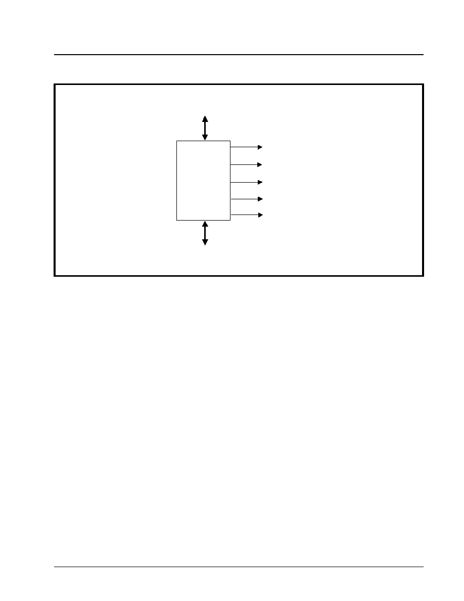
·Á
·Á
·Á
·Á
DS3 UNI FOR ATM
XRT7245
PRELIMINARY
REV. 1.03
249
7.3.2
Functional Description of Receive
Cell Processor
The Receive Cell Processor receives delineated
frames from the Receive PLCP Processor (or ATM
Cells from the Receive DS3 Framer). Once the
Receive Cell Processor receives this information
then it will proceed to perform the following functions.
∑
Cell Delineation
∑
HEC Byte Verification (Header Error Detection/
Correction)
∑
Idle Cell Filtering
∑
User Cell Filtering
∑ Cell Payload De-Scrambling
Each of these functions are discussed in detail below.
Figure 77 presents a functional block diagram of the
Receive Cell Processor.
F
IGURE
76. S
IMPLE
I
LLUSTRATION
OF
THE
R
ECEIVE
C
ELL
P
ROCESSOR
,
WITH
ASSOCIATED
P
INS
Receive Cell
Processor
RxCellRxed
RxGFCClk
RxGFCMSB
RxGFC
From Receive E3
Framer
To Receive Utopia
Interface Block
RxLCD
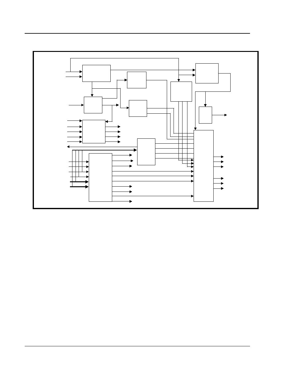
XRT7245
DS3 UNI FOR ATM
·Á
·Á
·Á
·Á
PRELIMINARY
REV. 1.03
250
7.3.2.1
Cell Delineation
The approach that the Receive Cell Processor will use
to perform cell-delineation depends upon whether the
UNI is operating in the "PLCP" mode (e.g., with the
PLCP Processors active) or in the "Direct-Mapped
ATM" mode (e.g., with the PLCP Processors disabled).
The cell-delineation process for each of these modes
are discussed below.
7.3.2.1.1
Cell Delineation while the UNI is
Operating in the PLCP Mode
The Receive PLCP Processor determines the frame
boundaries of the PLCP frame data that it receives
from the Receive DS3 Framer. Afterwards, the
Receive PLCP Processor will transfer these PLCP
frames, along with the frame boundary information to
the Receive Cell Processor.Table 55 presents the
byte-format of the PLCP frame. It is easy to see, from
this figure, that if the Receive Cell Processor is aware
of the locations of the boundaries of these PLCP
frames, then the comprising ATM cells are easily
located and thus delineated.
F
IGURE
77. F
UNCTIONAL
B
LOCK
D
IAGRAM
OF
THE
R
ECEIVE
C
ELL
P
ROCESSOR
6-Byte Buffer
HEC
CRC
Calculator
Error
Position
Calculator
Idle &
OAM Cell
Detector
Direct DS3
Nibble to Byte
Converter
OAM
Memory
Configuration
and
Status
Registers
De-Scrambler
Data
Path
Check
Controller
Delineation
and
Error
Correction
BufClk
BufDat[3:0]
RxCosetEn
HECErr
RxGFCClk
RxGFCStart
RxGFC
RFifoDat[7:0]
To Rx Utopia
RUSoC
RFifoWrClk
RFifoWrEnB
CSB*
WriteB*
ReadB*
RxCPRegSel
DataBusH[7:0]
DataBusL[7:0]
RxCPInt
CorrEn
RDPChkPat
RDPChkEn
OAM Extract
ICDiscard
HECErrIgnore
CorrThresh[1:0]
RxCosetEn
De-ScrEn
ICFound
OAMFound
CellCount[5:0]
OAM Write
OAM Cycle
OAMData[7:0]
RxCellClk_PLCP
RxCellDat_PLCP[7:0]
RxNbDat_Fr[3:0]
RxNbClk_Fr
DirectDS3
RxCellClk
RxCellDat[7:0]
BufDat[3:0]
BufClk
Ready
De-Scram
Data[7:0]
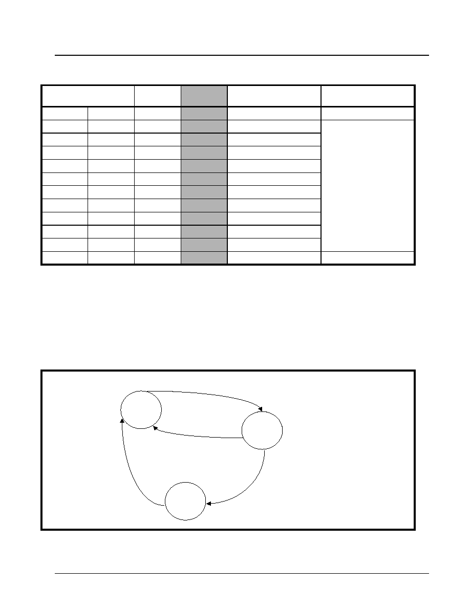
·Á
·Á
·Á
·Á
DS3 UNI FOR ATM
XRT7245
PRELIMINARY
REV. 1.03
251
7.3.2.1.2
Cell Delineation while the UNI is
Operating in the "Direct-Mapped
ATM" mode.
When the UNI is operating in the "Direct-Mapped
ATM" mode, then the Receive Cell Processor is
receiving unframed cell data from the Receive DS3
Framer. Therefore, the Receive Cell Processor will
have to use the "HEC Byte" Cell-Delineation algo-
rithm in order to locate the boundaries of these cells.
The HEC Byte Cell Delineation algorithm contains
three states: HUNT, PRESYNC, and SYNC, as
depicted in the State Machine Diagram in Figure 78.
Each of these states are discussed below. .
T
ABLE
55: B
YTE
-F
ORMAT
OF
THE
PLCP F
RAME
PLCP F
RAME
2 B
YTES
POI
1 B
YTE
POH
1 B
YTE
PLCP P
AYLOAD
53 B
YTES
A1
A2
P11
Z6
First ATM Cell
13≠14 nibbles
A1
A2
P10
Z5
ATM Cell
A1
A2
P9
Z4
ATM Cell
A1
A2
P8
Z3
ATM Cell
A1
A2
P7
Z2
ATM Cell
A1
A2
P6
Z1
ATM Cell
A1
A2
P5
X
ATM Cell
A1
A2
P4
B1
ATM Cell
A1
A2
P3
G1
ATM Cell
A1
A2
P2
X
ATM Cell
A1
A2
P1
X
ATM Cell
A1
A2
P0
C1
Twelfth ATM Cell
Trailer
F
IGURE
78. C
ELL
D
ELINEATION
A
LGORITHM
E
MPLOYED
BY
THE
R
ECEIVE
C
ELL
P
ROCESSOR
,
WHEN
THE
UNI
IS
OPERATING
IN
THE
"D
IRECT
-M
APPED
" ATM M
ODE
.
HUNT
PRESYNC
SYNC
Correct HEC
Incorrect HEC
DELTA Consecutive Correct
HEC at 53 Byte Intervals
ALPHA Consecutive
Incorrect HEC
XRT7245
DS3 UNI FOR ATM
·Á
·Á
·Á
·Á
PRELIMINARY
REV. 1.03
252
The HUNT State
When the UNI chip is first powered up and configured
to operate in the "Direct-Mapped ATM" mode, the
Receive Cell Processor will initially be operating in
the "HUNT" state. While the Receive Cell Processor
is operating in the "HUNT" state, it has no knowledge
of the location of the boundaries of the incoming
cells. In the HUNT state, the Receive Cell Processor
is searching through the incoming ("unframed") cell
data-stream for a possible valid cell header pattern
(e.g., one that does not produce a HEC byte error).
Therefore, while in this state, the Receive Cell
Processor will read in five octets of the data that it
receives from the Receive DS3 framer. The Receive
Cell Processor will then compute a "HEC byte value"
based upon the first four of these five octets. The
Receive Cell Processor will then compare this com-
puted value with that of the 5th "read-in" octet. If the
two values are not the same, then the Receive Cell
Processor will increment its sampling set (of the 5
bytes) by one bit, and repeat the above-process with
this new set of "candidate" header bytes. In other
words, the Receive Cell Processor make its next
selection of the five octets, 53 bytes and 1 bit later.
If the Receive Cell Processor comes across a set of
five octets, that are such that the computed HEC byte
value does match the 5th (read in) octet, then the
Receive Cell Processor will transition to the
PRESYNC state.
The PRE-SYNC State
The Receive Cell Processor will transition from the
"HUNT" state to the "PRESYNC" state; when it has
located an "apparently" valid set of cell header bytes.
However, it is possible that the Receive Cell Processor
is being "fooled" by user data that mimics the cell
header byte pattern. Therefore, further evaluation is
required in order to confirm that this set of octets are
truly valid cell header bytes. The purpose of the "PRE-
SYNC" state is to facilitate this "further evaluation."
When the Receive Cell Processor is operating in the
PRE-SYNC state, it will then begin to sample 5 "can-
didate header bytes" at 53 byte intervals. During this
sampling process, the Receive Cell Processor will
compute and compare its newly computed "HEC byte
value" with that of the fifth (read-in) octet. If the
Receive Cell Processor, while operating in the PRE-
SYNC state, comes across a single invalid cell header
byte pattern, then the Receive Cell Processor will
transition back to the "HUNT" state. However, if the
Receive Cell Processor detects "DELTA" consecutive
valid cell byte headers, then it will transition into the
SYNC state.
The SYNC State
The Receive Cell Processor will notify the local µP
(and external circuitry) of its transition to the SYNC
state by
∑
Generating a "Change of LCD (Loss of Cell Delin-
eation) State" interrupt. When the Receive Cell
Processor generates the "Change in LCD Condition"
interrupt, it will also set Bit 1 (LCD Interrupt Status)
within the "Rx CP Interrupt Status" Register, as
depicted below.
∑
Negating the RxLCD output pin (e.g., toggling it
"low"); and
∑ Setting bit 7 (Rx LCD) within the Rx CP Configura-
tion Register to "0".
The SYNC State
When the Receive Cell Processor is operating in the
SYNC state, it will tolerate some sporadic errors in the
cell header bytes and, in some cases, even attempt to
correct them. However, the occurrence of "ALPHA"
consecutive cells with header byte errors (single or
multi-bit), will cause the Receive Cell Processor to
return to the "HUNT" state. The Receive Cell Processor
will notify the external circuitry that is is not properly
delineating cells by doing the following.
∑
Generating a "Change in LCD State" interrupt.
∑
Assert the RxLCD output pin (e.g., toggling it
"high").
Rx CP Interrupt Status Register (Address = 4Eh)
B
IT
7
B
IT
6
B
IT
5
B
IT
4
B
IT
3
B
IT
2
B
IT
1
B
IT
0
Unused
Received OAM
Cell Interrupt
Status
LCD Interrupt
Status
HEC Error
Interrupt Status
RO
RO
RO
RO
RO
RUR
RUR
RUR
0
0
0
0
0
0
1
x
·Á
·Á
·Á
·Á
DS3 UNI FOR ATM
XRT7245
PRELIMINARY
REV. 1.03
253
∑ Setting bit 7 (Rx LCD) within the "Rx CP Configura-
tion Register" to "0", as depicted below.
The remaining discussion of the Receive Cell Pro-
cessor, within this data sheet, presumes that it (the
Receive Cell Processor) is operating in the "SYNC"
state and is properly delineating cells.
The Overall Cell Filtering/Processing Approach
within the Receive Cell Processor block
Once the Receive Cell Processor is properly delin-
eating cells then it will proceed to route these cells
through a series of "filters"; prior to allowing these
cells to be written to the RxFIFO within the Receive
UTOPIA Interface block.
The sequence of filtering/processing that each cell
must go through is listed below in sequential order.
∑
HEC Byte Verification
∑
Idle Cell Filtering
∑
User Cell Filteing
∑
Cell Payload De-Scrambling
∑ Inserting of the "Data Path Integrity Check" pattern
into the 5th octet of each cell.
This sequence of processing (within the Receive Cell
Processor) is also illustrated in Figure 79.
Each of these "Filtering/Processing" steps (within the
Receive Cell Processor) are discussed in detail below.
7.3.2.2
HEC Byte Verification
Once the Receive Cell Processor is properly delineat-
ing cells, the Receive Cell Processor will perform "HEC
Byte Verification" of incoming cell data from the
Receive PLCP Processor (or Receive DS3 Framer)
in order to protect against mis-routed or mis-inserted
cells. In performing HEC Byte Verification the Receive
Cell Processor will take the first four bytes of each
cell (e.g., the header bytes) and independently com-
pute its own value for the HEC byte. Afterwards, the
Receive Cell Processor will compare its value of the
HEC byte with the fifth octet that it has received from
the Receive PLCP Processor (or the Receive DS3
Framer). If the two HEC byte values match then the
Receive Cell Processor will retain this cell for further
processing. However, if the Receive Cell Processor
detects errors in the header bytes of a cell, then the
Receive Cell Processor will call up and employs the
"HEC Byte Error Correction/Detection" Algorithm
(see below).
The Receive Cell Processor will compute its version
of the HEC byte via the generating polynomial x
8
+ x
2
+ x + 1. The user should be aware that the HEC bytes
of the incoming cell might have been modulo-2 added
with the coset polynomial x
6
+ x
4
+ x
2
+ 1. If this is
the case then the Receive Cell Processor must be
configured to account for this by writing a "1" to Bit 1
(Rx Coset Enable) of the Rx CP Configuration Register;
as depicted below.
RxCP Configuration Register (Address = 4Ch)
B
IT
7
B
IT
6
B
IT
5
B
IT
4
B
IT
3
B
IT
2
B
IT
1
B
IT
0
RxLCD
RDPChk
Pattern
RDPChk
Pattern Enable
Idle Cell
Discard
OAM Check
Bit
De-Scramble
Enable
RxCoset
Enable
HEC Error
Ignore
RO
R/W
R/W
R/W
R/W
R/W
R/W
R/W
0
x
x
x
x
x
x
x
F
IGURE
79. I
LLUSTRATION
OF
O
VERALL
C
ELL
F
ILTERING
/P
ROCESSING
PROCEDURING
THE
OCCURS
WITHIN
THE
R
ECEIVE
C
ELL
P
ROCESSOR
HEC Byte
Verification
Idle Cell
Filtering
User Cell
Filtering
Insert Data
Path Integrity
Check Pattern
To RxFIFO
(within RxUtopia
InterfaceBlock)
Delineated Cells
From Rx
E3 Framer
XRT7245
DS3 UNI FOR ATM
·Á
·Á
·Á
·Á
PRELIMINARY
REV. 1.03
254
The "HEC Byte Error Correction/Detection"
Algorithm
If the Receive Cell Processor detects one or more
errors in the header bytes of a given cell, then the
"HEC Byte Error Correction/Detection" algorithm will be
employed. The "HEC Byte Error Correction/Detection"
Algorithm has two states: Detection and Correction.
Figure 80 presents a State Machine Diagram of the
"HEC Byte Error Correction/Detection" Algorithm.
Each of these states are discussed below.
The "Correction" State
When the "HEC Byte Correction/Detection" Algorithm
is operating in the Correction Mode; cells with single
bit errors (within the header bytes) will be corrected.
However, cells with multiple bit errors are discarded,
unless configured by the user. The user can configure
the Receive Cell Processor to retain these cells with
multi-bit errors, by writing to bit 0 (HEC Error Ignore) of
the Rx CP Configuration Register, as depicted below.
Writing a "1" into this bit-field causes the Receive Cell
Processor to retain errored cells for further processing.
Writing a "0" to this bit-field causes the Receive Cell
Processor to discard those cells with multi-bit errors.
Note: The occurrence of any cells with header byte errors
(single-bit or multi-bit errors) will cause the Receive Cell
Processor to transition from the "Correction" state to the
"Detection" state.
RxCP Configuration Register (Address = 4Ch)
B
IT
7
B
IT
6
B
IT
5
B
IT
4
B
IT
3
B
IT
2
B
IT
1
B
IT
0
RxLCD
RDPChk
Pattern
RDPChk
Pattern Enable
Idle Cell
Discard
OAM Check
Bit
De-Scramble
Enable
RxCoset
Enable
HEC Error
Ignore
RO
R/W
R/W
R/W
R/W
R/W
R/W
R/W
0
x
x
x
x
x
x
x
F
IGURE
80. S
TATE
M
ACHINE
D
IAGRAM
OF
THE
HEC B
YTE
E
RROR
C
ORRECTION
/D
ETECTION
A
LGORITHM
Correction
Mode
Detection
Mode
No Error
Detected
Multi-bit Error Detected
(Cell Discarded)
No Error Detected
for M consecutive cells
Single-bit Error Detected
(Cell Corrected)
Error Detected
(Cell Discarded)
Alpha consecutive cells with incorrect
HEC bytes (to HUNT state)
RxCP Configuration Register (Address = 4Ch)
B
IT
7
B
IT
6
B
IT
5
B
IT
4
B
IT
3
B
IT
2
B
IT
1
B
IT
0
RxLCD
RDPChk
Pattern
RDPChk
Pattern Enable
Idle Cell
Discard
OAM Check
Bit
De-Scramble
Enable
RxCoset
Enable
HEC Error
Ignore
RO
R/W
R/W
R/W
R/W
R/W
R/W
R/W
0
x
x
x
x
x
x
x
·Á
·Á
·Á
·Á
DS3 UNI FOR ATM
XRT7245
PRELIMINARY
REV. 1.03
255
Monitoring of Single-Bit Errors, during HEC Byte
Verification.
The user can monitor the number of Single Bit Errors
that have been detected by the Receive Cell Processor
during HEC Byte Verification. Each time the Receive
Cell Processor detects a Single-Bit error, the PMON
Received Single-Bit HEC Error Count registers are
incremented. These registers are located at addresses
2Eh and 2Fh and their bit-formats are presented below.
The contents of these registers reflect the total num-
ber of Single-Bit Errors that have been detected by
the Receive Cell Processor since the last read of this
register. These registers are reset upon read.
Monitoring of Multi-Bit Errors, during HEC Byte
Verification
The user can also monitor the number of Multiple Bit
Errors that have been detected by the Receive Cell
Processor, during HEC Byte Verification by reading the
PMON Received Multiple-Bit HEC Error Count Reg-
isters (Addresses = 30h and 31h). These registers are
incremented once for each incoming cell that contains
multiple (e.g., more than 1) bit-errors. The bit format
of these two registers follow.
The contents of these registers reflect the number of
cells with Multiple-Bit Errors that have been detected
by the Receive Cell Processor, during HEC Byte
Verification, since the last read of this register. These
registers are reset upon read.
PMON Received Single HEC Error Count--MSB (Address = 2Eh)
B
IT
7
B
IT
6
B
IT
5
B
IT
4
B
IT
3
B
IT
2
B
IT
1
B
IT
0
S-HEC Error Count--High Byte
RUR
RUR
RUR
RUR
RUR
RUR
RUR
RUR
0
0
0
0
0
0
0
0
PMON Received Single HEC Error Count--LSB (Address = 2Fh)
B
IT
7
B
IT
6
B
IT
5
B
IT
4
B
IT
3
B
IT
2
B
IT
1
B
IT
0
S-HEC Error Count--Low Byte
RUR
RUR
RUR
RUR
RUR
RUR
RUR
RUR
0
0
0
0
0
0
0
0
PMON Received Multiple-Bit HEC Error--MSB (Address = 30h)
B
IT
7
B
IT
6
B
IT
5
B
IT
4
B
IT
3
B
IT
2
B
IT
1
B
IT
0
M-HEC Error Count--High Byte
RUR
RUR
RUR
RUR
RUR
RUR
RUR
RUR
0
0
0
0
0
0
0
0
PMON Received Multiple-Bit HEC Error--LSB (Address = 31h)
B
IT
7
B
IT
6
B
IT
5
B
IT
4
B
IT
3
B
IT
2
B
IT
1
B
IT
0
M-HEC Error Count--Low Byte
RUR
RUR
RUR
RUR
RUR
RUR
RUR
RUR
0
0
0
0
0
0
0
0
XRT7245
DS3 UNI FOR ATM
·Á
·Á
·Á
·Á
PRELIMINARY
REV. 1.03
256
The "Detection" State
When the "HEC Byte Error Detection/Correction"
algorithm is operating in the Detection mode, then
all errored cells (e.g., those cells with single-bit errors
and multi-bit errors) will be discarded, unless config-
ured otherwise by the user. The user can configure
the Receive Cell Processor to retain errored cells by
writing to bit 0 (HEC Error Ignore) of the Rx CP
Configuration register (Address = 4Ch), as described
above.
The "HEC Byte Error Correction/Detection" Algorithm
will transition back into the "Correction" state once the
Receive Cell Processor has detected "M" consecutive
cells with the correct HEC byte values. The user has
the option to use the following values for "M": 0, 1, 3,
and 7. The user can configure the UNI to use any of
these values for M by writing the appropriate values
to the "RxCP Additional Configuration" Register
(Address = 4Dh), as depicted below.
The definition of the bits relevant to the "HEC Byte
Error Correction/Detection" algorithm follow:
Bit 1--Correction (Mode) Enable
This "Read/Write" bit field allows the user to enable/
disable the "Correction Mode" portion of the "HEC
Byte Error Correction/Detection" algorithm. If the user
writes a "0" to this bit-field, the "HEC Byte Error
Correction/Detection" algorithm will be disabled from
entry/operation in the "Correction" mode. Therefore,
the Receive Cell Processor will only operate in the
"Detection" mode. If the user writes a "1" to this bit
field then the "HEC Byte Error Correction/Detection"
algorithm will transition into and out of the "Correction"
as dictated by the "Correction Threshold".
Bits 2 and 3--Correction Threshold [1, 0]
These "Read/Write" bit-fields allow the user to select
the "Correction" Threshold for the "HEC Byte Error
Correction/Detection" algorithm. The following table
relates the content of these bit-fields to the Correction
Threshold Value (M). Once again, M is the number of
consecutive "Error-Free" cells that the Receive Cell
Processor must detect before the "HEC Byte Correc-
tion/Detection" algorithm will allow a transition back
into the "Correction" Mode.
7.3.2.3
Cell Filtering
As mentioned earlier, the Receive Cell Processor will fil-
ter (e.g., discard) incoming cells based upon the follow-
ing criteria.
∑
HEC Byte Errors (via the "HEC Byte Correction/
Detection" algorithm, as described in 7.3.2.2.)
∑
Idle Cells
∑
Header Byte Patterns--User Cells
∑ Segment OAM Cells
Each of these cell filtering approaches are presented
below.
Filtering of Cells with HEC Byte Errors
Please see the "HEC Byte Correction/Detection"
algorithm in Section 7.3.2.2.
7.3.2.3.1
Idle Cell Filtering
The user can configure the Receive Cell Processor
to either discard or retain Idle cells by writing to bit 4
(Idle Cell Discard) of the Rx CP Configuration Register,
as depicted below.
RxCP Additional Configuration Register (Address = 4Dh)
B
IT
7
B
IT
6
B
IT
5
B
IT
4
B
IT
3
B
IT
2
B
IT
1
B
IT
0
Unused
User Cell Filter
Discard
User Cell Filter
Enable
Correction Threshold [1, 0]
Correct
Enable
Unused
RO
RO
R/W
R/W
R/W
R/W
R/W
RO
T
ABLE
56: T
HE
R
ELATIONSHIP
BETWEEN
C
ORR
T
HRESHOLD
[1:0]
AND
THE
"C
ORRECTION
T
HRESHOLD
" V
ALUE
(M)
B
IT
3
B
IT
2
C
ORRECTION
T
HRESHOLD
V
ALUE
(M)
0
0
M = 0
0
1
M = 1
1
0
M = 3
1
1
M = 7
·Á
·Á
·Á
·Á
DS3 UNI FOR ATM
XRT7245
PRELIMINARY
REV. 1.03
257
If the user writes a "0" to this bit-field, then the Idle
Cells will be retained and will ultimately be sent on to
the User Cell Filter within the Receive Cell Processor
block. However, if the user writes a "1" to this bit-field,
then the Receive Cell Processor will discard all detect-
ed Idle-cells.
If the user wishes to have the Receive Cell Processor
discard the Idle Cells then he/she must specify the
header byte patterns of these Idle cells. The Idle Cell
header byte pattern is defined based upon the content
of 8 read/write registers. These eight registers are the
four "Rx CP Idle Cell Pattern Header byte registers,
and the four "Rx CP Idle Cell Mask Header--Byte"
Registers. In short, when a cell reaches the "Idle Cell
Filter" portion of the Receive Cell Processor, the
contents of each header byte of this cell (bytes 1
through 4), will be compared against the contents of
the corresponding "Rx CP Idle Cell Pattern Header
Byte" registers; based upon constraints specified by
the contents within the "Rx CP Idle Cell Mask Header
Byte" registers. The use of these registers in "Idle
Cell Identification" and filtering is illustrated in the
example below.
Example--Idle Cell Filtering
For example, header byte 1 of a given incoming cell
(which may be an Idle cell or a User cell) will be sub-
jected to a bit-by-bit comparison to the contents of
the "Rx CP Idle Cell Pattern Header Byte-1" register
(Address = 50h). The purpose of having the Receive
Cell Processor perform this comparison is to deter-
mine if this incoming cell is an Idle Cell or not. The
contents of the "Rx CP Idle Cell Mask Header Byte-1"
register (Address = 54h) also plays a role in this com-
parison process. For instance, if bit-field "0" within the
"Rx CP Idle Cell Mask Header Byte-1" register
contains a "1", then the Receive Cell Processor will
perform the comparison operation between bit-field
"0" within the "Rx CP Idle Cell Pattern Header Byte-1"
register; and bit-field "0" within header byte 1 of the
newly received cell. Conversely, if bit-field "0" within
the "Rx CP Idle Cell Mask Header Byte-1" register
contains a "0", then this comparison will not be made
and bit-field "0" will be treated as a "don't care". The
role of these two read/write registers, in these compar-
ison operations is more clearly defined in Table 57,
below.
RxCP Configuration Register (Address = 4Ch)
B
IT
7
B
IT
6
B
IT
5
B
IT
4
B
IT
3
B
IT
2
B
IT
1
B
IT
0
RxLCD
RDPChk
Pattern
RDPChk
Pattern Enable
Idle Cell
Discard
OAM Check
Bit
De-Scramble
Enable
RxCoset
Enable
HEC Error
Ignore
RO
R/W
R/W
R/W
R/W
R/W
R/W
R/W
0
x
x
x
x
x
x
x
T
ABLE
57: I
LLUSTRATION
OF
THE
R
OLE
OF
THE
"R
X
CP I
DLE
C
ELL
P
ATTERN
H
EADER
B
YTE
" R
EGISTER
,
AND
THE
"R
X
CP I
DLE
C
ELL
M
ASK
H
EADER
B
YTE
" R
EGISTER
Content of Header Byte-1 (of Incoming Cell)
B
IT
7
B
IT
6
B
IT
5
B
IT
4
B
IT
3
B
IT
2
B
IT
1
B
IT
0
1
0
1
0
0
1
0
1
Content of "Rx CP Idle Cell Mask Header Byte-1 Register
B
IT
7
B
IT
6
B
IT
5
B
IT
4
B
IT
3
B
IT
2
B
IT
1
B
IT
0
1
1
1
1
0
0
0
0
Content of "Rx CP Idle Cell Header Byte-1 Register
B
IT
7
B
IT
6
B
IT
5
B
IT
4
B
IT
3
B
IT
2
B
IT
1
B
IT
0
1
0
1
0
1
1
0
1
XRT7245
DS3 UNI FOR ATM
·Á
·Á
·Á
·Á
PRELIMINARY
REV. 1.03
258
Based upon these register settings, any cell containing
values in the range of A0h≠AFh are considered to be
matching the "Idle Cell Pattern", at the first byte. This
incoming cell will be subjected to three (3) more tests
(e.g., one for each of the remaining header bytes) be-
fore it is identified as an Idle Cell or not.
Consequently, if the user opts to "discard" Idle Cells,
then any cells, passing the above-described tests,
will be identified as an Idle Cell and will be discarded
by the Receive Cell Processor.
The bit format for each of these eight "Idle Cell" iden-
tification registers are listed below.
Comments
B
IT
7
B
IT
6
B
IT
5
B
IT
4
B
IT
3
B
IT
2
B
IT
1
B
IT
0
Comparison is Forced (by the "1s" in the Rx CP Idle Cell
Mask Header Byte-1 Register)
Don't Care
Don't Care
Don't Care
Don't Care
Results of Comparison
B
IT
7
B
IT
6
B
IT
5
B
IT
4
B
IT
3
B
IT
2
B
IT
1
B
IT
0
1
0
1
0
x
x
x
x
T
ABLE
57: I
LLUSTRATION
OF
THE
R
OLE
OF
THE
"R
X
CP I
DLE
C
ELL
P
ATTERN
H
EADER
B
YTE
" R
EGISTER
,
AND
THE
"R
X
CP I
DLE
C
ELL
M
ASK
H
EADER
B
YTE
" R
EGISTER
(C
ONT
'
D
)
Rx CP Idle Cell Pattern Header Byte-1 Register (Address = 50h)
B
IT
7
B
IT
6
B
IT
5
B
IT
4
B
IT
3
B
IT
2
B
IT
1
B
IT
0
Rx Idle Cell Pattern--Header Byte 1
R/W
R/W
R/W
R/W
R/W
R/W
R/W
R/W
0
0
0
0
0
0
0
0
Rx CP Idle Cell Pattern Header Byte-2 Register (Address = 51h)
B
IT
7
B
IT
6
B
IT
5
B
IT
4
B
IT
3
B
IT
2
B
IT
1
B
IT
0
Rx Idle Cell Pattern--Header Byte 2
R/W
R/W
R/W
R/W
R/W
R/W
R/W
R/W
0
0
0
0
0
0
0
0
Rx CP Idle Cell Pattern Header Byte-3 Register (Address = 52h)
B
IT
7
B
IT
6
B
IT
5
B
IT
4
B
IT
3
B
IT
2
B
IT
1
B
IT
0
Rx Idle Cell Pattern--Header Byte 3
R/W
R/W
R/W
R/W
R/W
R/W
R/W
R/W
0
0
0
0
0
0
0
0

·Á
·Á
·Á
·Á
DS3 UNI FOR ATM
XRT7245
PRELIMINARY
REV. 1.03
259
The user can periodically monitor the number of Idle
Cells that have been detected by the Receive Cell Pro-
cessor, by reading the PMON Received Idle Cell Count
Register (Addresses = 32h, 33h). The bit-format of
these registers are presented below.
Rx CP Idle Cell Pattern Header Byte-4 Register (Address = 53h)
B
IT
7
B
IT
6
B
IT
5
B
IT
4
B
IT
3
B
IT
2
B
IT
1
B
IT
0
Rx Idle Cell Pattern--Header Byte
R/W
R/W
R/W
R/W
R/W
R/W
R/W
R/W
0
0
0
0
0
0
0
0
Rx CP Idle Cell Mask Header--Byte 1 (Address = 54h)
B
IT
7
B
IT
6
B
IT
5
B
IT
4
B
IT
3
B
IT
2
B
IT
1
B
IT
0
Rx Idle Cell Mask Header--Byte 1
R/W
R/W
R/W
R/W
R/W
R/W
R/W
R/W
1
1
1
1
1
1
1
1
Rx CP Idle Cell Mask Header--Byte 2 (Address = 55h)
B
IT
7
B
IT
6
B
IT
5
B
IT
4
B
IT
3
B
IT
2
B
IT
1
B
IT
0
Rx Idle Cell Mask Header--Byte 2
R/W
R/W
R/W
R/W
R/W
R/W
R/W
R/W
1
1
1
1
1
1
1
1
Rx CP Idle Cell Mask Header--Byte 3 (Address = 56h)
B
IT
7
B
IT
6
B
IT
5
B
IT
4
B
IT
3
B
IT
2
B
IT
1
B
IT
0
Rx Idle Cell Mask Header--Byte 3
R/W
R/W
R/W
R/W
R/W
R/W
R/W
R/W
1
1
1
1
1
1
1
1
Rx CP Idle Cell Mask Header--Byte 4 (Address = 57h)
B
IT
7
B
IT
6
B
IT
5
B
IT
4
B
IT
3
B
IT
2
B
IT
1
B
IT
0
Rx Idle Cell Mask Header--Byte 1
R/W
R/W
R/W
R/W
R/W
R/W
R/W
R/W
1
1
1
1
1
1
1
1
XRT7245
DS3 UNI FOR ATM
·Á
·Á
·Á
·Á
PRELIMINARY
REV. 1.03
260
The content of these registers are the number of Idle
Cells that have been detected, by the Receive Cell
Processor, since the last read of these registers.
These registers are reset upon read.
7.3.2.3.2
User Cell Filtering
The user can configure the Receive Cell Processor
to filter incoming user or OAM cells based upon the
value of their header bytes. The UNI provides the
user with three (3) options.
∑
Disable the User Cell Filter.
∑
Pass only those cells with header byte patterns
matching the settings of the User Cell Filter.
∑ Discard only those cells with header byte patterns
matching the settings of the User Cell Filter.
Each of these User-Cell Filtering Options are
discussed below.
Disable the User-Cell Filter
If the user disables the User-Cell Filter, within the
Receive Cell Processor, then all user cells (indepen-
dent of their header byte patterns) will be written into
the Rx FIFO, within the Receive UTOPIA Interface
block.
Writing a "1" to Bit 4 (User Cell Filter Enable) enables
the User Cell Filter. Whereas, writing a `0" to this bit-field
disables the User Cell Filter.
Enable the User Cell Filter
If the User Cell Filter is enabled, then the Receive
Cell Processor will be filtering user cells in one of two
possible manners.
1.
Pass Only those cells with header bytes patterns
matching the User Cell Filter settings (e.g., the
contents of the "Rx CP User Cell Filter Pattern
Header Byte" registers), or
2.
Discard only those cells with header byte patterns
matching the User Cell Filter settings.
The User (or Assigned) cell filtering criteria is defined
based upon the contents of 8 read/write registers.
These eight registers are the four "Rx CP User Cell
Filter Pattern Header byte" registers and the four "Rx
CP User Cell Filter Mask Header Byte" registers. In
short, when a user cell reaches the Receive Cell
Processor, the contents of each header byte of this
cell (bytes 1 through 4), will be compared against the
contents of the corresponding "Rx CP User Cell Filter
Pattern Header Byte" registers based upon constraints
specified by the contents of the "Rx CP User Cell
PMON Received Idle Cell Count--MSB (Address = 32h)
B
IT
7
B
IT
6
B
IT
5
B
IT
4
B
IT
3
B
IT
2
B
IT
1
B
IT
0
Rx Idle Cell Count--High Byte
RO
RO
RO
RO
RO
RO
RO
RO
0
0
0
0
0
0
0
0
PMON Received Idle Cell Count--LSB (Address = 33h)
B
IT
7
B
IT
6
B
IT
5
B
IT
4
B
IT
3
B
IT
2
B
IT
1
B
IT
0
Rx Idle Cell Count--Low Byte
RO
RO
RO
RO
RO
RO
RO
RO
0
0
0
0
0
0
0
0
RxCP Additional Configuration Register (Address = 4Dh)
B
IT
7
B
IT
6
B
IT
5
B
IT
4
B
IT
3
B
IT
2
B
IT
1
B
IT
0
Unused
User Cell Filter
Discard
User Cell Filter
Enable
Correction Threshold [1, 0]
Correction
Enable
Unused
RO
RO
R/W
R/W
R/W
R/W
R/W
RO
·Á
·Á
·Á
·Á
DS3 UNI FOR ATM
XRT7245
PRELIMINARY
REV. 1.03
261
Filter Mask Header Byte" registers. The role of these
registers in "User Cell Filtering" is illustrated in the
example below.
Example--User Cell Filtering
For example, header byte 1 of a given incoming user
cell will be subjected to a bit-by-bit comparison to the
contents of the "Rx CP User Cell Filter Pattern Header
Byte-1" register (Address = 58h). However, the con-
tents of the "Rx CP User Cell Filter Mask Header
Byte-1" register (Address = 5Ch) also plays a role in
this comparison process. For example, if bit-field "0"
within the "Rx CP User Cell Filter Mask Header Byte-1"
register contains a "1", then the Receive Cell Processor
will perform the comparison operation between bit-
field "0" within the "Rx CP User Cell Filter Pattern
Header Byte-1" register; and bit-field "0" within header
byte 1 of the newly received user cell. Conversely, if
bit-field `0' within the "Rx CP User Cell Filter Mask
Header Byte-1" register contains a `0', then this com-
parison will not be made and bit-field `0' will be treated
as a `don't care'. The role of these two read/write reg-
isters in these comparison operations is more clearly
defined in Table 58, on following page.
Based upon these register settings, any cell containing
values in the range of A0h≠AFh are considered to be
matching, at the first byte. This cell will be subjected to
three (3) more tests (e.g., one for each of the remain-
ing header bytes.)
After all of these comparison tests have been
performed, a given user cell will be deemed either
"matching" or "not matching" the settings of the User
Cell Filter. Once the cell has been classified into one
of these two categories, its disposition (or fate) is
dependent upon the content of bit-field 5 (User Cell
Filter Discard) within the "Rx CP Additional Configu-
ration Register (Address = 4Dh). If this bit-field is `0',
then only-matching cells will be retained, and written
into the RxFIFO. All remaining User Cells will be
discarded. Conversely, it this bit-field is `1', then only
`non-matching' User Cells will be retained and written
T
ABLE
58: I
LLUSTRATION
OF
THE
R
OLE
OF
THE
"R
X
CP U
SER
C
ELL
F
ILTER
P
ATTERN
H
EADER
B
YTE
"
REGISTER
AND
THE
"R
X
CP U
SER
C
ELL
F
ILTER
M
ASK
H
EADER
B
YTE
"
REGISTER
.
Content of Header Byte-1 (of Incoming User Cell)
B
IT
7
B
IT
6
B
IT
5
B
IT
4
B
IT
3
B
IT
2
B
IT
1
B
IT
0
1
0
1
0
0
1
0
1
Content of "Rx CP User Cell Filter Mask Header Byte-1 Register
B
IT
7
B
IT
6
B
IT
5
B
IT
4
B
IT
3
B
IT
2
B
IT
1
B
IT
0
1
1
1
1
0
0
0
0
Content of "Rx CP User Cell Filter Pattern Header Byte-1 Register
B
IT
7
B
IT
6
B
IT
5
B
IT
4
B
IT
3
B
IT
2
B
IT
1
B
IT
0
1
1
1
1
0
0
0
0
Comments
B
IT
7
B
IT
6
B
IT
5
B
IT
4
B
IT
3
B
IT
2
B
IT
1
B
IT
0
Comparison is Forced (by the "1s" in the Rx CP User Cell Fil-
ter Mask Header Byte-1 Register)
Don't Care
Don't Care
Don't Care
Don't Care
Resulting "User Cell Fiilter" Pattern for Header Byte-1
B
IT
7
B
IT
6
B
IT
5
B
IT
4
B
IT
3
B
IT
2
B
IT
1
B
IT
0
1
0
1
0
x
x
x
x

XRT7245
DS3 UNI FOR ATM
·Á
·Á
·Á
·Á
PRELIMINARY
REV. 1.03
262
to the RxFIFO. All `matching' User Cells will be
discarded.
The bit-formats of the 8 registers that define the User
Cell Filtering criteria are presented below.
User Cell Filter Header Byte Pattern Registers
User Cell Filter Mask Registers
Rx CP User Filter Cell Pattern Header--Byte 1 (Address = 58h)
B
IT
7
B
IT
6
B
IT
5
B
IT
4
B
IT
3
B
IT
2
B
IT
1
B
IT
0
Rx User Cell Header Pattern--Byte 1
R/W
R/W
R/W
R/W
R/W
R/W
R/W
R/W
0
0
0
0
0
0
0
0
Rx CP User Filter Cell Pattern Header--Byte 2 (Address = 59h)
B
IT
7
B
IT
6
B
IT
5
B
IT
4
B
IT
3
B
IT
2
B
IT
1
B
IT
0
Rx User Cell Header Pattern--Byte 2
R/W
R/W
R/W
R/W
R/W
R/W
R/W
R/W
0
0
0
0
0
0
0
0
Rx CP User Filter Cell Pattern Header--Byte 3 (Address = 5Ah)
B
IT
7
B
IT
6
B
IT
5
B
IT
4
B
IT
3
B
IT
2
B
IT
1
B
IT
0
Rx User Cell Header Pattern--Byte 3
R/W
R/W
R/W
R/W
R/W
R/W
R/W
R/W
0
0
0
0
0
0
0
0
Rx CP User Filter Cell Pattern Header--Byte 4 (Address = 5Bh)
B
IT
7
B
IT
6
B
IT
5
B
IT
4
B
IT
3
B
IT
2
B
IT
1
B
IT
0
Rx User Cell Header Pattern--Byte 4
R/W
R/W
R/W
R/W
R/W
R/W
R/W
R/W
0
0
0
0
0
0
0
0
Rx CP User Filter Cell Mask Header--Byte 1 (Address = 6Eh)
B
IT
7
B
IT
6
B
IT
5
B
IT
4
B
IT
3
B
IT
2
B
IT
1
B
IT
0
Rx User Cell Mask Header--Byte 1
R/W
R/W
R/W
R/W
R/W
R/W
R/W
R/W
1
1
1
1
1
1
1
1

·Á
·Á
·Á
·Á
DS3 UNI FOR ATM
XRT7245
PRELIMINARY
REV. 1.03
263
7.3.2.4
OAM Cell Processing
OAM (Operation Administration and Maintenance)
cells, are special cells that are generated by the "Lay-
er Management" entity (within the BISDN Reference
Model), and are typically used to carry maintenance
related information such as:
∑
Virtual Path Connection (VPC)/Virtual Circuit
Connection (VCC) failure reporting
∑
VPC/VCC continuity check information
∑
VPC/VCC continuity verification: OAM Cell
Loopback Testing
∑ VPC/VCC Performance Monitoring
OAM cells are identified and distinguished from user
cells by their specific cell header byte patterns. ATM
layer entities can typically use one of four types of
OAM cells. These types of OAM cells are listed below.
∑
F4--Segment
∑
F4--End to End
∑
F5--Segment
∑ F5--End to End
F4 type OAM cells usually carry maintenance related
information regarding a specific Virtual Path Connection
(VPC). Whereas F5 type OAM cells usually carry main-
tenance related regarding a specific Virtual Circuit
Connection (VCC). The header byte patterns of each
of these types of OAM cells is tabulated below.
Rx CP User Filter Cell Mask Header--Byte 2 (Address = 5Dh)
B
IT
7
B
IT
6
B
IT
5
B
IT
4
B
IT
3
B
IT
2
B
IT
1
B
IT
0
Rx User Cell Mask Header--Byte 2
R/W
R/W
R/W
R/W
R/W
R/W
R/W
R/W
1
1
1
1
1
1
1
1
Rx CP User Filter Cell Mask Header--Byte 3 (Address = 5Eh)
B
IT
7
B
IT
6
B
IT
5
B
IT
4
B
IT
3
B
IT
2
B
IT
1
B
IT
0
Rx User Cell Mask Header--Byte 3
R/W
R/W
R/W
R/W
R/W
R/W
R/W
R/W
1
1
1
1
1
1
1
1
Rx CP User Filter Cell Mask Header--Byte 4 (Address = 5Fh)
B
IT
7
B
IT
6
B
IT
5
B
IT
4
B
IT
3
B
IT
2
B
IT
1
B
IT
0
Rx User Cell Mask Heade--Byte 4
R/W
R/W
R/W
R/W
R/W
R/W
R/W
R/W
1
1
1
1
1
1
1
1
XRT7245
DS3 UNI FOR ATM
·Á
·Á
·Á
·Á
PRELIMINARY
REV. 1.03
264
where: a--bit is available for use by the ATM layer entity
z--Any VCI value other than 0
As far as the XRT7245 DS3 UNI IC is concerned,
whether an OAM cell is an F4 or F5 type OAM cell,
is rather unimportant. The Receive Cell Processor
circuitry has been designed to recognize both types
of OAM cells, based upon their header byte pattern.
However, whether an OAM cell is a "Segment type"
or an "End-to-End type" is more important in regards
to UNI IC operation. The manner in which the
Receive Cell Processor handles "Segment" and
"End-to-End" OAM cells is described below.
7.3.2.4.1
Segment Type OAM Cells
Segment type OAM cells are only intended for point-
to-point transmission. In other words, a segment type
OAM cell will be created at a source node, transmis-
sion across a single link, to a destination node; and
then terminated at the destination node. This Segment
OAM cell is not intended to be read or processed by
any other nodes within the ATM Network.
How the Receive Cell Processor handles Segment
Type OAM Cells
The Receive Cell Processor has been designed to
recognize incoming OAM cells, based upon their
header byte pattern. Further, the Receive Cell
Processor is also capable of reading the header byte
patterns, in order to determine if the OAM cell is a
"Segment" type or an End-to-End type OAM cell. If
the incoming OAM cell is a "Segment" type OAM cell,
then the Receive Cell Processor will not write this cell
to the Rx FIFO, within the Receive UTOPIA Interface
block and will discard this cell. This act of discarding
the OAM cell terminates it and prevents it from prop-
agating to other nodes in the network.
Note: If the user configures the User Cell Filter to pass
cells with header bytes pattern ranges that includes that of
the "Segment"-type OAM Cell, then the User Cell Filter
settings will take precedence and allow the "Segment"-type
OAM Cell to be written to the Rx FIFO, within the Receive
UTOPIA Interface Block.
Although the Receive Cell Processor will discard this
"Segment" OAM cell, the user can configure the
Receive Cell Processor to have the contents of this
cell written into the Receive OAM Cell Buffer, where it
can be read out and processed by the local µP/µC.
If the user writes a "1" to bit 3 (OAM Check Bit) within
the "Rx CP Configuration" register (Address = 4Ch),
then all OAM cells that are received by the Receive
Cell Processor will be written into the Receive OAM
Cell buffer (located at 161h through 1A1h, in the UNI
chip address space).
Once the Receive Cell Processor has written the
OAM cell into the "Receive OAM Cell" buffer, then the
Receive Cell Processor will alert the local µP/µC of
this fact, by generating the "Received OAM Cell"
interrupt. If the user write a "0" to bit 3 of the "Rx CP
Configuration" register, then the Receive Cell
Processor will not write the contents of the OAM cells
that it receives, to the "Receive OAM Cell" buffer.
T
ABLE
59: T
HE
H
EADER
B
YTE
P
ATTERN
FORMATS
FOR
THE
V
ARIOUS
T
YPES
OF
OAM C
ELLS
OAM C
ELL
O
CTET
1
O
CTET
2
O
CTET
3
O
CTET
4
F4 End-to-End
0000aaaa
aaaa0000
00000000
01000a0a
F4 Segment
0000aaaa
aaaa0000
00000000
00110a0a
F5 End-to-End
0000aaaa
aaaazzzz
zzzzzzzz
zzzz101a
F5 Segment
0000aaaa
aaaazzzz
zzzzzzzz
zzzz100a
RxCP Configuration Register (Address = 4Ch)
B
IT
7
B
IT
6
B
IT
5
B
IT
4
B
IT
3
B
IT
2
B
IT
1
B
IT
0
RxLCD
RDPChk
Pattern
RDPChk
Pattern Enable
Idle Cell
Discard
OAM Check
Bit
De-Scramble
Enable
RxCoset
Enable
HEC Error
Ignore
RO
R/W
R/W
R/W
R/W
R/W
R/W
R/W
0
x
x
x
x
x
x
x
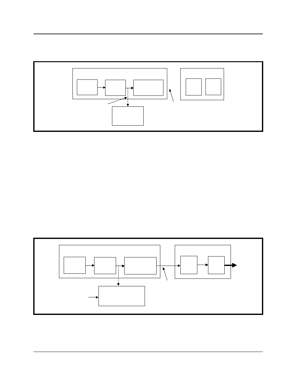
·Á
·Á
·Á
·Á
DS3 UNI FOR ATM
XRT7245
PRELIMINARY
REV. 1.03
265
Figure 81 presents an illustration depicting how the
Receive Cell Processor handles incoming Segment-
type OAM cells, if the user has written a "1" to bit 3
(OAM Check Bit) of the "Rx CP Configuration" register.
7.3.2.4.2
End-to-End Type OAM Cells
"End-to-End" type OAM cells, as the name implies, are
intended for something more than a point-to-point trans-
mission. In other words, an end-to-end type OAM cell
will be created at a source node, transmitted across a
single link, to a destination node. However, in this
case, the "end-to-end" OAM cell is not terminated at
this destination node; but is rather transmitted across
other links to other nodes within the network.
How the Receive Cell Processor Handles End-to-
End type OAM Cells
If the Receive Cell Processor determines that the in-
coming OAM Cell is an "End-to-End" type then it will
be written into the Rx FIFO, within the Receive UTOPIA
Interface block. This act will allow the ATM Layer
processor to read in this OAM cell, from the UNI and
propagate this cell to other nodes in the network.
Note: The Receive Cell Processor will write the "End-to-
End" OAM cell to the Rx FIFO, independent of the User
Cell Filter settings.
The user can also configure the Receive Cell Processor
to write the contents of the "End-to-End" OAM cell
into the Receive OAM Cell Buffer. For details on how
this can be done, please see Section 7.3.2.4.1.
Figure 82 presents an illustration which depicts how
the Receive Cell Processor handles incoming End-
to-End type OAM Cells, if the user has written a "1" to
bit 3 (OAM Check Bit) of the "Rx CP Configuration"
register.
Monitoring the Number of User/OAM Cells
The user can monitor the number of Valid cells (User
and OAM) that have been received by the Receive
Cell Processor, by reading the PMON Received Valid
Cell Count Registers (Address = 34h, and 35h). The
bit-format of these registers are presented below.
F
IGURE
81. A
N
A
PPROACH
TO
P
ROCESSING
S
EGMENT
OAM
CELLS
,
VIA
THE
R
ECEIVE
C
ELL
P
ROCESSOR
.
User Cell Filter
Receive Cell Processor
Rx FIFO
Receive Utopia Block
Cell
Delineation
HEC
Verification
Utopia
Interface
Path of OAM Cell
OAM Cell Buffer
Located at Address
(161h - 1A1h) in on-
Chip RAM.
OAM Cell is not "passed
through" to the Rx FIFO in
the Receive Utopia Block
F
IGURE
82. A
PPROACH
TO
P
ROCESSING
"E
ND
-
TO
-E
ND
" OAM C
ELLS
User Cell Filter
Receive Cell Processor
Rx FIFO
Receive Utopia Interface Block
Cell
Delineation
HEC
Verification
Utopia
Interface
Receive OAM Cell Buffer
Located at Address
(161h - 1A1h) in on-
Chip RAM.
"End-to-End" Type OAM
Cell is "passed through" to
the Rx FIFO in the Receive
Utopia Interface Block
The Contents of
the OAM Cell are
also written into
the "Receive OAM
Cell" buffer
XRT7245
DS3 UNI FOR ATM
·Á
·Á
·Á
·Á
PRELIMINARY
REV. 1.03
266
The contents of this register reflect the total number of
valid cells that the Receive Cell Processor has received
since the last reading of this register. This register is
reset upon read.
Finally, the user can also monitor the total number of
cells that have been discarded (either due to HEC
errors, Idle Cell removal, or User cell filtering) by
reading the PMON Discarded Cell Count Registers
(Address = 36h, 37h). The bit-format of this register
is presented below.
The contents of these registers reflect the number of
cells that have been discarded since the last read of
these registers. These registers are reset upon read.
7.3.2.5
Cell Payload De-Scrambling
In numerous applications the payload portion of the
incoming cells will be scrambled by the Transmit Cell
Processor, within the Far End Transmitting terminal.
These cells are scrambled in order to prevent the user
data from mimicking framing or control bytes. There-
fore, the Receive Cell Processor provides the user
will the option of de-scrambling the payload of these
cells in order to restore the original content of the cell
payload. (Please note that this cell de-scrambler
presumes that the cell payload were scrambled via
the scrambling generating polynomial of x
43
+ 1.) The
user can configure this option by writing a "1" to Bit 2
(De-Scramble Enable) of the Rx CP Configuration
Register, as depicted below.
PMON Received Valid Cell Count--MSB (Address = 34h)
B
IT
7
B
IT
6
B
IT
5
B
IT
4
B
IT
3
B
IT
2
B
IT
1
B
IT
0
Rx Valid Cell Count--High Byte
RUR
RUR
RUR
RUR
RUR
RUR
RUR
RUR
0
0
0
0
0
0
0
0
PMON Received Valid Cell Count--LSB (Address = 35h)
B
IT
7
B
IT
6
B
IT
5
B
IT
4
B
IT
3
B
IT
2
B
IT
1
B
IT
0
Rx Valid Cell Count--Low Byte
RUR
RUR
RUR
RUR
RUR
RUR
RUR
RUR
0
0
0
0
0
0
0
0
PMON Discarded Cell Count--MSB (Address = 36h)
B
IT
7
B
IT
6
B
IT
5
B
IT
4
B
IT
3
B
IT
2
B
IT
1
B
IT
0
Cell Drop Count--High Byte
RUR
RUR
RUR
RUR
RUR
RUR
RUR
RUR
0
0
0
0
0
0
0
0
PMON Discarded Cell Count--LSB (Address = 37h)
B
IT
7
B
IT
6
B
IT
5
B
IT
4
B
IT
3
B
IT
2
B
IT
1
B
IT
0
Cell Drop Count--Low Byte
RUR
RUR
RUR
RUR
RUR
RUR
RUR
RUR
0
0
0
0
0
0
0
0
·Á
·Á
·Á
·Á
DS3 UNI FOR ATM
XRT7245
PRELIMINARY
REV. 1.03
267
7.3.2.6
Data Path Integrity Check
The "Data Path Integrity" check is a test that is
continually run in order to verify that the connections
throughout the "ATM Layer" entity (e.g., from the
Receive UTOPIA Interface of the "source" UNI to the
Transmit UTOPIA Interface of the "destination" UNI)
are functioning properly.
The manner in which the "Data Path Integrity Check"
is employed is as follows. After an incoming cell has
passed through the cell delineation, HEC byte verifi-
cation, idle cell filtering and user cell filtering process,
it will be written to the Rx FIFO, within the Receive
UTOPIA Interface Block. However, prior to being writ-
ten into the Rx FIFO, the "Data Path Integrity Test"
pattern will be written into the 5th octet (overwriting
the HEC byte) of the "outbound" cell. This "Data Path
Integrity Test" pattern is typically of the value "55h",
for each outbound cell. However, it can also be
configured to be an alternating pattern of "55h" and
AAh" (alternating values with each cell).
The Transmit Cell Processor, within the "destination"
UNI will perform a check of the 5th byte of all cells
that it reads from the Tx FIFO; prior to computing and
overwriting this byte with the HEC byte. For more
information on how the Transmit Cell Processor
andles the "Data Path Integrity Check" test patterns,
please see section 6.2.2.6.
The Receive Cell Processor's Handling of the
Data Path Integrity Test pattern
The user has a variety of options, when it comes to
configuring the Receive Cell Processor to support
the Data Path Integrity Test. First of all, the user can
decide whether or not he/she wishes to even transmit
a Data Path Integrity Test pattern, via the outbound
cell; or just allow the outbound cell with the HEC byte
to be written to the Rx FIFO. The user can configure
the Receive Cell Processor per his/her choice, by
writing the appropriate value into bit 5 (RDPChk
Pattern Enable) within the "Rx CP Configuration
Register (Address = 4Ch) as depicted below.
Writing a "1" to this bit-field configures the Receive
Cell Processor to write the "Data Path Integrity Test"
pattern into the 5th octet of each "outbound" cell,
prior to transmittal to the RxFIFO. Conversely, writing
a "0" to this bit-field configures the Receive Cell
Processor to write the cell, with the HEC byte, into
the RxFIFO.
Next, the Receive Cell Processor also allows the user
to choose between two possible Data Path Integrity
Test patterns. The user can configure his/her selection
by writing the appropriate value to Bit 6 (RDPChk
Pattern) within the "Rx CP Configuration" Register
(Address = 4Ch). Writing a "1" to this bit-field config-
ures the Receive Cell Processor to write a "55h" into
the 5th octet of each "outbound" cell, prior to it being
written into the Rx FIFO. Conversely, writing a "0" to
this bit-field configures the Receive Cell Processor to
write an alternating pattern of "55h" or "AAh", into the
5th octet of each "outbound" cell, prior to it being writ-
ten into the RxFIFO. The Receive Cell Processor will
alternate between each of these two patterns with
each "outbound" cell.
Note: The contents of Bit 6 of the Rx CP Configuration
Register, is ignored if Bit 5 is set to "0".
RxCP Configuration Register (Address = 4Ch)
B
IT
7
B
IT
6
B
IT
5
B
IT
4
B
IT
3
B
IT
2
B
IT
1
B
IT
0
RxLCD
RDPChk
Pattern
RDPChk
Pattern
Enable
Idle Cell
Discard
OAM Check
Bit
De-Scramble
Enable
RxCoset
Enable
HEC Error
Ignore
RO
R/W
R/W
R/W
R/W
R/W
R/W
R/W
0
x
x
x
x
x
x
x
RxCP Configuration Register (Address = 4Ch)
Bit 7
Bit 6
Bit 5
Bit 4
Bit 3
Bit 2
Bit 1
Bit 0
RxLCD
RDPChk
Pattern
RDPChk
Pattern Enable
Idle Cell
Discard
OAM Check
Bit
De-Scramble
Enable
RxCoset
Enable
HEC Error
Ignore
RO
R/W
R/W
R/W
R/W
R/W
R/W
R/W
0
x
x
x
x
x
x
x
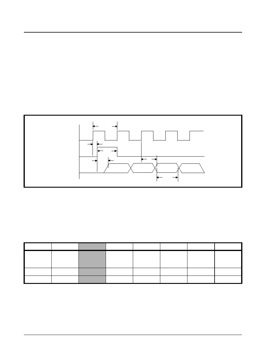
XRT7245
DS3 UNI FOR ATM
·Á
·Á
·Á
·Á
PRELIMINARY
REV. 1.03
268
7.3.2.7
GFC Nibble Extraction--via the RxGFC
Serial Output Port
The first four bit-field of each cell header are the GFC
bits. The Receive Cell processor will output the con-
tents of the GFC Nibble-field for each cell that it re-
ceives, via the "GFC Nibble Field" serial output port.
The "Receive GFC Nibble-Field" serial output port
consists of the following pins.
∑
RxGFC
∑
RxGFCClk
∑ RxGFCMSB
The data is output via the RxGFC output pin. The or-
der of transmission, within a given cell, is with the
MSB first and in descending order until transmitting
the LSB bit. Afterwards, the "GFC Nibble-field" serial
output port will output the MSB for the GFC Nibble-
field of the next cell. This data is clocked out on the
rising edge of the RxGFCClk output signal. The RxG-
FCMSB output pin will be pulsed "high" each time the
MSB of the GFC Nibble field, for a given cell, is
present at the RxGFC input. Figure 83 presents an il-
lustration depicting the behavior of the RxGFC Serial
Output Port signals.
7.3.2.8
Receive Cell Processor Interrupts
The Receive Cell Processor will generate interrupts
upon
∑
HEC Errors
∑
OAM Cell received
∑ Loss of Cell Delineation
If one of these conditions occur, and if that particular
condition is enabled for interrupt generation, then
when the local µC/µP reads the UNI Interrupt Status
Register, as shown below, it should read `xx1xxxxxb'
(where the -b suffix denotes a binary expression, and
`x' denotes a "don't care" value).
At this point, the local µC/µP will have determined that
the Receive Cell Processor block is the source of the
interrupt, and that the Interrupt Service Routine
should branch accordingly. In order to accomplish
this the local µC/µP should now read the "Rx CP Inter-
rupt Status Register" (Address = 4Fh). The bit format
of this register is presented below.
F
IGURE
83. I
LLUSTRATION
OF
THE
B
EHAVIOR
OF
THE
R
X
GFC S
ERIAL
O
UTPUT
P
ORT
SIGNALS
RxGFCClk
RxGFCMSB
t52
RxGFC
BIT 3
BIT 2
BIT 1
BIT 0
t50
t48
t51
t47
t49
UNI Interrupt Status Register (Address = 05h)
B
IT
7
B
IT
6
B
IT
5
B
IT
4
B
IT
3
B
IT
2
B
IT
1
B
IT
0
RxDS3
Interrupt
Status
RxPLCP
Interrupt
Status
RxCP
Interrupt
Status
Rx UTOPIA
Interrupt
Status
Tx UTOPIA
Interrupt
Status
TxCP
Interrupt
Status
TxDS3
Interrupt
Status
One Sec
Interrupt
Status
RO
RO
RO
RO
RO
RO
RO
RUR
x
x
1
x
x
x
x
x
·Á
·Á
·Á
·Á
DS3 UNI FOR ATM
XRT7245
PRELIMINARY
REV. 1.03
269
The bit format of the Rx CP Interrupt Status Register
indicates that only three (3) bit-fields within this register
are active. The role of each of these bit fields follows.
Bit 0--HEC Byte Error Interrupt Status
A "1" in this "Reset-upon-Read" bit-field indicates the
Receive Cell Processor has detected a HEC Byte
error in an incoming cell, and has requested a "HEC
Byte Error" Interrupt, since the last read of this register.
Bit 1--"Change in LCD (Loss of Cell Delineation)
State" Interrupt Status
A "1" in this "Reset-upon-Read" bit-field indicates that
the Receive Cell Processor has changed its "LCD"
(Loss of Cell Delineation) state and has issued the
"Change in LCD State" interrupt, since the last read
of this register.
Note: This type of interrupt could occur due to a transition
from the SYNC state to the HUNT state, in the "HEC Byte
Cell Delineation Algorithm"; during which the RxLCD pin
will toggle "high". Additionally, this type of interrupt could
also occur due to the transition from the PRE-SYNC state
into the SYNC state. The user can distinguish between
these two possibilities by reading the RxLCD bit-field (bit 7) in
the Rx CP Configuration Register (Address = 4Ch).
Bit 2--Received OAM Cell Interrupt Status
A "1" in this "Reset-upon-Read" bit-field indicates that
the Receive Cell Processor has detected an OAM
Cell in the path of "incoming cells"; and has stored
the contents of this OAM cell in the "Receive OAM
Cell Buffer", since the last read of this register. The
purpose of this interrupt is to alert the local µP/µC
that the "Receive OAM Cell Buffer" (within the UNI)
contains an OAM cell that needs to be read and
processed.
7.4
Receive UTOPIA Interface Block
7.4.1
Brief Description of the Receive UTOPIA
Interface Block
The Receive UTOPIA Interface Block provides a
"UTOPIA Level 2" compliant interface to interconnect
the UNI chip to ATM layer or ATM Adaptation Layer
processors, operating up to 800 Mbps. This interface
supports both an 8 and 16 bit wide data bus. Since
data is received at clock rates independent of the
ATM layer clock rate, the received cell data is written
into an internal FIFO by the Receive Cell Processor
block. This FIFO will be referred to as the Rx FIFO
throughout this document. The Receive Cell Processor
will delineate, check for HEC byte errors, filter and
de-scramble ATM Cells. Whatever cells were not
discarded by the Receive Cell Processor will be
written into the Rx FIFO, where it can be read out
from the UNI device by the ATM Layer Processor.
The Receive UTOPIA Interface Block will inform the
ATM Layer processor that it has cell data available for
reading, by asserting the RxClav pin "high". Figure 84
on the following page presents a simple illustration of
the Receive UTOPIA Interface block and the
associated pins.
7.4.2
Functional Description of Receive UTOPIA
The purposes of the Receive UTOPIA Interface block
are to:
∑
Receive filtered ATM cell data from the Receive
Cell Processor and make this data available to the
AAL or ATM Layer Processor.
Rx CP Interrupt Status Register (Address = 4Ch)
B
IT
7
B
IT
6
B
IT
5
B
IT
4
B
IT
3
B
IT
2
B
IT
1
B
IT
0
Unused
Received OAM
Cell Interrupt
Status
LCD
Interrupt Status
HEC Error
Interrupt Status
RO
RO
RO
RO
RO
RUR
RUR
RUR
F
IGURE
84. S
IMPLE
B
LOCK
D
IAGRAM
OF
R
ECEIVE
UTOPIA B
LOCK
OF
UNI.
Receive Utopia
Interface
RxClk
RxEnB
RxPrty
RxData[15:0]
RxSoC
RxClav/RxEmptyB*
RxAddr[4:0]
From Receive Cell Processor

XRT7245
DS3 UNI FOR ATM
·Á
·Á
·Á
·Á
PRELIMINARY
REV. 1.03
270
∑
Inform the ATM Layer Processor whenever the
RxFIFO contains cell data that needs to be read.
∑
Inform the ATM Layer Processor that it has no
more cell data to be read.
∑
Compute and present the odd-parity value of the
byte (or word) that is present at the Receive UTOPIA
Data Bus.
∑ Indicate the boundaries of cells, to the ATM Layer
processor, by pulsing the RxSoC (Receive Start of
Cell) pin each time the first byte (or word) of a new
cell is present on the Receive UTOPIA Data Bus.
The Receive UTOPIA Interface Block consists of the
following sub-blocks:
∑
Receive UTOPIA Output Interface
∑
Receive UTOPIA Cell FIFO (Rx FIFO)
∑ Receive UTOPIA FIFO Manager
The Receive UTOPIA Interface block consists of an
output interface complying to the "UTOPIA Level 2
Interface Specifications", and the RxFIFO. The width
of the Receive UTOPIA Data Bus is user-configurable
to be either 8 or 16 bits. The Receive UTOPIA Inter-
face block also allows the ATM Layer processor to
perform parity checking on all data that it receives
from it (the Receive UTOPIA Interface block), over
the Receive UTOPIA Data bus. The Receive UTOPIA
Interface block computes the odd-parity of each byte
(or word) that it will place on the Receive UTOPIA
data bus. The Receive UTOPIA Interface block will
then output the value of this computed parity at the
RxPrty pin, while the corresponding data byte (word)
is present at the RxData[15:0] output pins.
The Receive UTOPIA Interface block can be config-
ured to process 52, 53, and 54 bytes per cell; and will
assert the RxSoC (Receive "Start of Cell") output pin
at the cell boundaries. If the Receive UTOPIA Inter-
face block detects a "runt" cell (e.g., a cell that is
smaller than what the Receive UTOPIA Interface
block has been configured to handle), it will generate
an interrupt to the local µP, discard this "runt" cell,
and resume normal operation.
The physical size of the Rx FIFO is four cells. The
incoming data (from the Receive Cell Processor) is
written into the Rx FIFO, where it can be read in and
processed by the ATM Layer Processor. A FIFO Man-
ager maintains the Rx FIFO and indicates the FIFO
Empty and FIFO Full to the local µP. Additionally the
FIFO Manager will indicate that ATM Cell Data is
available in the RxFIFO, by asserting the RxClav out-
put pin. Figure 85 presents a Functional Block Diagram
of the Receive UTOPIA Interface Block.
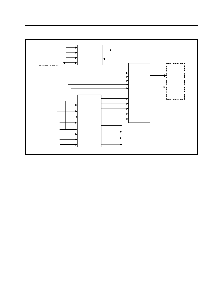
·Á
·Á
·Á
·Á
DS3 UNI FOR ATM
XRT7245
PRELIMINARY
REV. 1.03
271
The following sections discuss each functional sub-
block of the Receive UTOPIA Interface block in detail.
Additionally, these sections discuss many of the fea-
tures associated with the Receive UTOPIA Interface
block as well as how the user can optimize these
features in order to suit his/her application needs.
Detailed discussion of Single-PHY and Multi-PHY
operation will be presented in its own section even
though it involves the use of all of these functional
blocks.
7.4.2.1
Receive UTOPIA Bus Output Interface
The Receive UTOPIA output interface complies with
the UTOPIA Level 2 standard interface (e.g., the
Receive UTOPIA can support both Single-PHY and
Multi-PHY operations). Additionally, the UNI provides
the user with the option of varying the following features
associated with the Receive UTOPIA Bus interface.
∑
Receive UTOPIA Data Bus width of 8 or 16 bits.
∑ The cell size (e.g., the number of octets being
processed per cell via the UTOPIA bus)
A discussion of the operation of the Receive UTOPIA
Bus Interface along with each of these options will be
presented below.
7.4.2.1.1
The Pins of the Receive UTOPIA Bus
Interface
The ATM Layer processor will interface to the Receive
UTOPIA Interface block via the following pins.
∑
RxData[15:0]--Receive UTOPIA Data Bus output
pins.
∑
RxAddr[4:0]--Receive UTOPIA Address Bus input
pins.
∑
RxClk--Receive UTOPIA Interface Block clock
input pin.
∑
RxSoC--Receive "Start of Cell" Indicator output
pin.
∑
RxPrty--Receive UTOPIA--Odd Parity output pin.
∑
RxEnB*--Receive UTOPIA Data Bus--Output
Enable input pin.
∑ RxClav/RxFullB*--RxFIFO Cell Available output
pin.
F
IGURE
85. F
UNCTIONAL
B
LOCK
D
IAGRAM
OF
THE
R
ECEIVE
UTOPIA I
NTERFACE
B
LOCK
RxUtopia
Registers
D[15:0]
A[8:0]
Status Signals
Control Signals
Rx Utopia
FIFO Manager
Rx Utopia
Cell FIFO
RxData[15:0]
RxData[7:0]
RxAddr[4:0]
RxEnB
RxSoC
RxClk
RxUtopia Interrupt
RxClav/RxEmptyB
Controls from
Registers
RxFWrClk
RWrEnB
(To Pin)
(To Interrupt block)
Read
Write
RxFData[7:0]
RxData[7:0]/
RxData[15:0]
RxSoC
Status Bits to Registers
RxPrty
To Pins
From Rx CP

XRT7245
DS3 UNI FOR ATM
·Á
·Á
·Á
·Á
PRELIMINARY
REV. 1.03
272
Each of these signals are discussed below.
RxData[15:0]--Receive UTOPIA Data Bus Out-
puts
The ATM Layer Processor will read ATM cell data
from the Receive UTOPIA Interface block in a byte-
wide (or word-wide) manner, via these output pins.
The Receive UTOPIA Data bus can be configured to
operate in the "8 bit wide" or "16 bit wide" mode (See
Section 7.4.2.1.2). If the "8-bit wide" mode is selected,
then only the RxData[7:0] output pins will be active
and capable of transmitting data. If the 16-bit wide
mode is selected, then all 16 output pins (e.g.,
RxData[15:0]) will be active. The Receive UTOPIA
Data bus is tri-stated while the active low RxEnB*
(Receive UTOPIA Bus--Output Enable) input signal
is "high". Therefore, the ATM Layer Processor must
assert this signal (e.g., toggle RxEnB* low) in order
to read the ATM cell data from the Receive UTOPIA
Interface block. The data on the Receive UTOPIA
Data Bus output pins are updated on the rising edge
of the Receive UTOPIA Interface block clock signal,
RxClk.
RxAddr[4:0]--Receive UTOPIA Address Bus In-
puts
These input pins are used only when the UNI is oper-
ating in the Multi-PHY mode. Therefore, for more
information on the Receive UTOPIA Address Bus,
please see Section 7.4.2.2.2.2.
RxClk--Receive UTOPIA Interface Block--Clock
Signal Input Pin
The Receive UTOPIA Interface block uses this signal
to update the data on the Receive UTOPIA Data Bus.
The Receive UTOPIA Interface block also uses this
signal to sample and latch the data on the Receive
UTOPIA Address bus pins (during Multi-PHY opera-
tion), into the Receive UTOPIA Interface block circuitry.
This clock signal can run at frequencies of 25 MHz,
33 MHz, or 50 MHz.
RxEnB*--Receive UTOPIA Data Bus--Output
Enable Input
The Receive UTOPIA Data bus is tri-stated while this
input signal is negated. Therefore, the user must assert
this "active-low" signal (toggle it "low") in order to
read the byte (or word) from the Receive UTOPIA
Interface block via the Receive UTOPIA Data bus.
RxPrty--Receive UTOPIA--Odd Parity Bit
Output Pin
The Receive UTOPIA Interface Block will compute
the odd-parity of each byte (or word) of ATM cell data
that it will place on the Receive UTOPIA Data bus.
The Receive UTOPIA Data bus will output the value
of the computed parity bit at the RxPrty output pin,
while the corresponding byte (or word) is present on
the Receive UTOPIA Data Bus. This features allows
the ATM Layer Processor to perform parity checking
on the data that it receives from the Receive UTOPIA
Interface Block.
RxSoC--Receive UTOPIA--"Start of Cell"
Indicator Output Pin
The Receive UTOPIA Interface block will pulse this
output signal "high", for one clock period of RxClk,
when the first byte (or word) of a new cell is present
on the Receive UTOPIA Data Bus. This signal will be
"low" at all other times.
RxClav/RxEmptyB*--Rx FIFO Cell Available/
RxEmpty*
This output signal is used to alert the ATM Layer
Processor that the Rx FIFO contains some ATM cell
data that is available for reading. Please see Section
7.4.2.2.1 for more information regarding this signal.
7.4.2.1.2
Selecting the UTOPIA Data Bus Width
The UTOPIA data bus width can be selected to be
either 8 or 16 bits by writing the appropriate data into
the UtWidth16 bit (bit 0) within the UTOPIA Configu-
ration Register, as shown below.
If the user chooses a UTOPIA Data Bus width of
8 bits, then only the Receive UTOPIA Data output
pins: RxData[7:0] will be active. (The output
pins:RxData[15:8] will not be active). If the user
chooses a UTOPIA Data bus width of 16 bits, then all
of the Receive UTOPIA Data outputs: RxData[15:0]
will be active. The following table relates the value of
Bit 0 (UtWidth) within the UTOPIA Configuration
Register, to the corresponding width of the UTOPIA
Data bus.
UTOPIA Configuration Register: (Address = 6Ah)
B
IT
7
B
IT
6
B
IT
5
B
IT
4
B
IT
3
B
IT
2
B
IT
1
B
IT
0
Unused
Handshake Mode
M-PHY
CellOf52 Bytes
TFIFODepth[1, 0]
UtWidth16
RO
R/W
R/W
R/W
R/W
R/W
·Á
·Á
·Á
·Á
DS3 UNI FOR ATM
XRT7245
PRELIMINARY
REV. 1.03
273
Note:
1. The selection of this bit also affects the width of the
Transmit UTOPIA Data bus.
2. The UTOPIA Data Bus width will be 8 bits, upon
power up or reset. Therefore, the user must write a
"1" to this bit in order to set the width of the
Receive UTOPIA (and the Transmit UTOPIA data
bus) to 16 bits.
7.4.2.1.3
Selecting the Cell Size (Number of
Octets per Cell)
The UNI allows the user to select the number of oc-
tets per cell that the Receive UTOPIA Interface block
will process. Specifically, the user has the following
cell size options.
∑
If the UTOPIA Data Bus is 8 bits wide then the user
can choose:
≠ 52 bytes (with no HEC byte in the cell), or
≠ 53 bytes (with either a dummy or actual HEC
byte in the cell)
∑
If the UTOPIA Data Bus is 16 bits wide then the
user can choose:
≠ 52 bytes (with no HEC byte in the cell), or
≠ 54 bytes (with either a dummy or actual HEC
byte, and a stuff byte in the cell)
The user makes his/her selection by writing the appro-
priate data to bit 3 (CellOf52Bytes) within the UTOPIA
Configuration Register, as depicted below.
The following table specifies the relationship between
the value of this bit and the number of octets/cell that
the Receive UTOPIA Interface block will process.
Note: This selection applies to both the Transmit UTOPIA
and Receive UTOPIA interface blocks. Additionally, the
shaded selection reflects the default condition upon power
up or reset.
An Advisory to Users
The user must insure that the ATM Layer processor
only reads in (from the Receive UTOPIA Interface
block) the "configured" number of octets per cell,
following the latest assertion of the RxSoC output
pin. If the ATM Layer processor continues to try to
read-in more octets, it will end up reading in in-valid
data.
T
ABLE
60: T
HE
R
ELATIONSHIP
BETWEEN
THE
CONTENTS
WITHIN
B
IT
0 (U
T
W
IDTH
16)
WITHIN
THE
UTOPIA
C
ONFIGURATION
R
EGISTER
,
AND
THE
OPERATING
WIDTH
OF
THE
UTOPIA D
ATA
B
US
V
ALUE
FOR
U
T
W
IDTH
16
W
IDTH
OF
UTOPIA D
ATA
B
US
0
8 bit wide Data Bus
1
16 bit wide Data Bus
UTOPIA Configuration Register: (Address = 6Ah)
B
IT
7
B
IT
6
B
IT
5
B
IT
4
B
IT
3
B
IT
2
B
IT
1
B
IT
0
Unused
Handshake Mode
M-PHY
CellOf52 Bytes
TFIFODepth[1, 0]
UtWidth16
RO
R/W
R/W
R/W
R/W
R/W
T
ABLE
61: T
HE
R
ELATIONSHIP
BETWEEN
THE
VALUE
OF
B
IT
3 (C
ELL
O
F
52B
YTES
)
WITHIN
THE
UTOPIA
C
ONFIGURATION
R
EGISTER
,
AND
THE
NUMBER
OF
OCTETS
PER
CELL
THAT
WILL
BE
PROCESSED
BY THE
T
RANSMIT
AND
R
ECEIVE
UTOPIA I
NTERFACE
BLOCKS
.
C
ELL
O
F
52 B
YTES
N
UMBER
OF
B
YTES
/C
ELLS
0
53 bytes when the UTOPIA Data Bus width is 8 bits wide.
54 bytes when the UTOPIA Data Bus width is 16 bits wide.
1
52 bytes, regardless of the width of the UTOPIA Data Bus

XRT7245
DS3 UNI FOR ATM
·Á
·Á
·Á
·Á
PRELIMINARY
REV. 1.03
274
7.4.2.1.4
Parity Checking Handling of Errored
Cell Data received from the Receive
UTOPIA Interface Block
The Receive UTOPIA Interface block will compute the
odd parity of each byte (or word) of ATM cell data it
places on the Receive UTOPIA Data bus. The Receive
UTOPIA Interface block will also output the value of
this parity bit via the RxPrty pin. The RxPrty pin will
contain the odd parity value of the byte or word that is
residing on the Receive UTOPIA Data bus.
The user has the option to configure the ATM Layer
processor hardware and or software to use this feature.
7.4.2.2
Receive UTOPIA FIFO Manager
The Rx FIFO Manager has the following
responsibilities.
∑
Monitoring the fill level of the RxFIFO, and alerting
the ATM Layer processor anytime the RxFIFO
contains cell data that needs to be read.
∑
Detecting and discarding "Runt" cells and insuring
that the RxFIFO can resume normal operation
following the removal of the "Runt" cell.
∑
Insuring that the RxFIFO can respond properly to
an "Overrun" condition, by generating the "RxFIFO
Overrun Condition" interrupt, discarding the result-
ing "Runt" or errored cell, and resuming proper
operation afterwards.
∑
Generating the "RxFIFO Underrun Condition" inter-
rupt to the local µP, when the RxFIFO has been
depleted of ATM cell data.
Receive UTOPIA FIFO Manager Features and
Options
This section discusses the numerous features that
are provided by the Receive UTOPIA FIFO Manager.
Additionally, this section discusses how the user can
optimize these features to suit his/her application
needs.
The Receive UTOPIA FIFO Manager provides the
user with the following options.
∑
Handshaking Mode (Octet Level vs Cell Level)
∑
Resetting the Rx FIFO
∑
Monitoring the Rx FIFO
7.4.2.2.1
Selecting the Handshaking Mode
(Octet Level vs Cell Level)
The Receive UTOPIA Interface block offers two differ-
ent data flow control modes for data transmission be-
tween the ATM Layer processor and the UNI IC.
These two modes are: "Octet-Level" Handshaking
and "Cell-Level" Handshaking; as specified by the
UTOPIA Level 2, Version 8 Specifications, and are
discussed below.
7.4.2.2.1.1
Octet-Level Handshaking
The UNI will be operating in the Cell-Level Hand-
shaking Mode following power up or reset. Therefore,
the user will have to set bit 5 (Handshake Mode) within
the UTOPIA Configuration Register to "0" in order to
configure the UNI into "Octet-Level" Handshake Mode.
The main signal that is responsible for data-flow control
between the ATM Layer processor and the Receive
UTOPIA Interface block is the RxClav output pin.
When the UNI is operating in the Octet-Level Hand-
shake mode, the Receive UTOPIA Interface block will
assert the RxClav output pin, when the Rx FIFO con-
tains at least one "read cycle's" worth of ATM Cell
Data. In other words, if the UTOPIA Data bus width is
configured to be 16 bits wide, then the RxClav signal
will be asserted when the RxFIFO contains at least
two bytes of cell data. Likewise, if the UTOPIA Data
bus width is configured to be 8 bits wide, then the
RxClav signal will be asserted when the RxFIFO
contains at least one byte of ATM cell data. The
Receive UTOPIA Interface block will negate RxClav
when the Rx FIFO has been depleted of any data.
Therefore, the RxClav pin exhibits a role that is similar
to a "Ready Ready" indicator in RS-232 based data
transmission systems.
The ATM Layer processor is expected to monitor the
state of the RxClav pin very closely (either in a tightly
polled or interrupt driven approach). The ATM Layer
processor is also expected to respond very quickly to
the assertion of RxClav and read out the cell data in
order to avoid an "Overrun Condition" in the Rx FIFO.
Finally, the ATM Layer processor is expected to do
one of two things, whenever RxClav toggles "low".
1.
Quickly halting its reading of data from the
Receive UTOPIA data bus.
2.
Or, "validate" each byte or word of ATM cell data
that it reads from the Receive UTOPIA Data bus,
by checking the level of the RxClav signal. In this
case, the ATM Layer processor must have the
ability to internally remove any ATM cell data
bytes or words that have been read in, after
RxClav has toggled "low".
Figure 86 presents a timing diagram illustrating the
behavior of the RxClav pin during reads from the
Receive UTOPIA Interface block, while operating in
the Octet-Level Handshaking Mode.
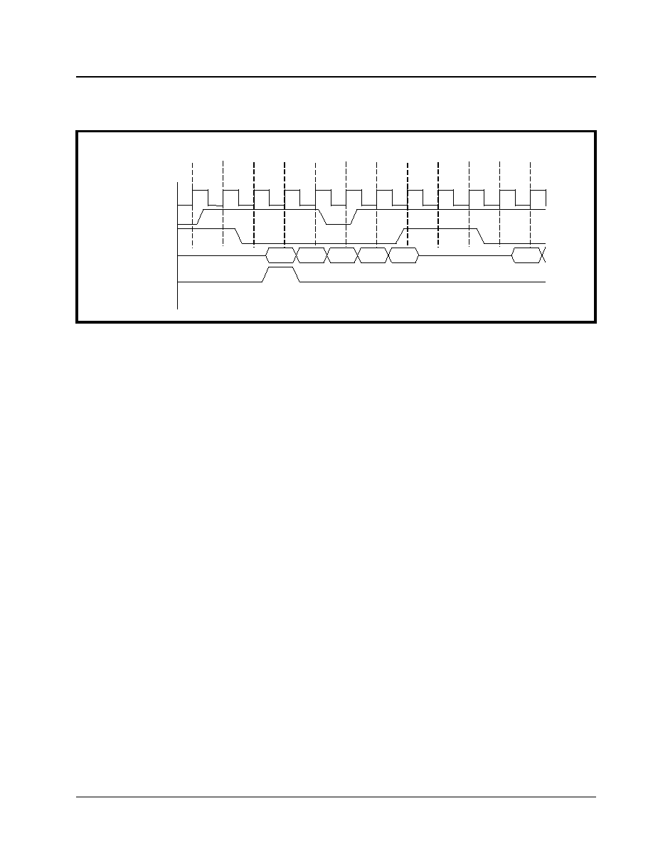
·Á
·Á
·Á
·Á
DS3 UNI FOR ATM
XRT7245
PRELIMINARY
REV. 1.03
275
Note: regarding Figure 86
1. The Receive UTOPIA Data bus is configured to be
16 bits wide. Hence, the data which the Receive
UTOPIA Interface block places on the Receive
UTOPIA Data bus is expressed in terms of 16 bit
words (e.g., W0≠W26).
2. The Receive UTOPIA Interface block is configured
to handle 54 bytes/cell. Hence, Figure 86 illustrates
the ATM Layer processor reading 27 words (W0
through W26) for each ATM cell.
In Figure 86, RxClav is initially "low" during clock edge
#1. However, shortly after clock edge 1, the RxFIFO
receives ATM cell data from the Receive Cell Processor
block. At this point, the RxClav signal toggles "high"
indicating that the RxFIFO contains at least one
"read-cycle" worth of cell data. The ATM Layer pro-
cessor will detect this "assertion of RxClav" during
clock edge #2. Consequently, in order to begin read-
ing this cell data, the ATM Layer processor will then
assert the RxEnB* input pin. At clock edge #3, the
Receive UTOPIA Interface block detects RxEnB*
being "low". Hence, the Receive UTOPIA Interface
block then places word W0 on the Receive UTOPIA
Data bus. The ATM Layer processor latches and
reads in W0, upon clock edge #4. In this figure,
shortly after the ATM Layer processor has read in
word W1 (at clock edge #5), the RxFIFO is depleted
which causes RxClav to toggle "low". In this figure,
the ATM Layer processor will keep the RxEnB* signal
asserted, and will read in an "invalid" word which is
denoted by the "X" in Figure 86. Shortly thereafter,
the RxFIFO receives some additional cell data from
the Receive Cell Processor, which in turn causes
RxClav to toggle "high". The ATM Layer processor
then continues to read in words W2 and W3. After-
wards, the ATM Layer processor is unable to continue
reading the ATM cell data from the Receive UTOPIA
Interface block; and subsequently negates the RxEnB*
signal; at clock edge #8. The Receive UTOPIA Inter-
face block detects that RxEnB* is "high" at clock edge
#8, and in turn, tri-states the Receive UTOPIA Data
Bus at around clock edge # 9. Finally, prior to clock
edge #11, the ATM Layer processor is able to resume
reading in ATM cell data from the Receive UTOPIA
Interface block, and indicates this fact by asserting
the RxEnB* (e.g., toggling it "low"). The Receive
UTOPIA Interface block detects this state change at
clock edge #11 and subsequently places word W4 on
the Receive UTOPIA Data bus.
7.4.2.2.1.2
Cell Level Handshaking
The UNI will be operating in the "Cell-Level" Hand-
shaking mode following power up or reset. In the
"Cell-Level" Handshaking mode, when the RxClav
output is at a logic "1", it means that the Rx FIFO
contains at least one complete ATM cell of data that
is available for reading by the ATM Layer Processor.
When RxClav toggles from "high" to "low", it indicates
that Rx FIFO contains less than one complete ATM
cell. As in the "Octet-Level" Handshake mode, the ATM
Layer processor is expected to monitor the RxClav
output, and quickly respond and read the Rx FIFO,
whenever the RxClav output signal is asserted.
The UNI can operate in either the "Octet-Level" or
"Cell-Level" Handshake mode, when operating in the
Single-PHY mode. However, only the Cell-Level
Handshake Mode is available when the UNI is oper-
ating in the Multi-PHY mode. For more information on
Single PHY and Multi PHY operation, please see
Section 7.4.2.2.2.
F
IGURE
86. T
IMING
D
IAGRAM
OF
R
X
C
LAV
/R
X
E
MPTY
B
AND
VARIOUS
OTHER
SIGNALS
DURING
READS
FROM
THE
R
ECEIVE
UTOPIA,
WHILE
OPERATING
IN
THE
O
CTET
-L
EVEL
H
ANDSHAKING
M
ODE
.
RxClk
RxClav
RxEnB*
RxData[15:0]
RxSoC
W2
W3
W4
X
W1
W0
1
2
3
4
5
6
7
8
9
10
11
12
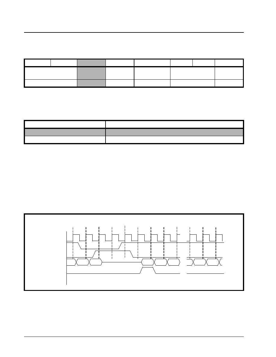
XRT7245
DS3 UNI FOR ATM
·Á
·Á
·Á
·Á
PRELIMINARY
REV. 1.03
276
The user can configure the UNI to operate in one of
these two handshake modes by writing the appropri-
ate data to Bit 5 (Handshake Mode) of the UTOPIA
Configuration Register, as depicted below.
The following table specifies the relationship between
this bit and the corresponding Handshaking Mode.
Note:
1. The Handshake Mode selection applies to both the
Transmit UTOPIA and Receive UTOPIA Interface
blocks.
2. Since Multi-PHY mode operation requires the use
of "Cell-Level" Handshaking; this bit is ignored if
the UNI is operating in the Multi-PHY mode.
3. Finally, the UNI will be operating in the "Cell-Level"
Handshaking Mode upon power up or reset.
Therefore, the user must write a "0" to this bit in
order to configure "Octet- Level Handshaking, mode.
Figure 87 presents a timing diagram that illustrates
the behavior of various Receive UTOPIA Interface
block signals when the Receive UTOPIA Interface
block is operating in the "Cell Level" Handshake Mode.
Note: regarding Figure 88
1. The Receive UTOPIA Data bus is configured to be
16 bits wide. Hence, the data, which the Receive
UTOPIA places on the Receive UTOPIA Data bus,
is expressed in terms of 16 bit words: W0≠W26.
2. The Receive UTOPIA Interface block is configured
to handle 54 bytes/cell. Hence, Figure 88 illustrates
the ATM Layer processor reading in 27 words (W0
through W26) for each ATM cell.
In Figure 88, the ATM Layer processor is just finishing
up its reading of an ATM cell. Prior to clock edge #2,
the RxFIFO does not contain enough ATM cell data
to make up at least one cell. Hence, the Receive
UTOPIA Configuration Register: Address = 6Ah
B
IT
7
B
IT
6
B
IT
5
B
IT
4
B
IT
3
B
IT
2
B
IT
1
B
IT
0
Unused
Handshake
Mode
M-PHY
CellOf52 Bytes
TFIFODepth[1, 0]
UtWidth16
R/W
R/W
R/W
R/W
R/W
R/W
T
ABLE
62: T
HE
R
ELATIONSHIP
BETWEEN
THE
CONTENTS
OF
B
IT
5 (H
ANDSHAKE
M
ODE
)
WITHIN
THE
UTOPIA
C
ONFIGURATION
R
EGISTER
,
AND
THE
RESULTING
UTOPIA I
NTERFACE
H
ANDSHAKE
M
ODE
V
ALUE
R
ESULTING
H
ANDSHAKE
M
ODE
0
The UTOPIA Interfaces operate in the cell level handshake mode.
1
The UTOPIA Interfaces operate in the octet level handshake mode.
F
IGURE
87. T
IMING
D
IAGRAM
OF
VARIOUS
R
ECEIVE
UTOPIA I
NTERFACE
BLOCK
SIGNALS
,
WHEN
THE
R
ECEIVE
UTOPIA I
NTERFACE
BLOCK
IS
OPERATING
IN
THE
"C
ELL
L
EVEL
" H
ANDSHAKE
M
ODE
RxClk
RxClav
RxEnB*
RxData[15:0]
RxSoC
W24
W25
W26
W0
W1
W2
W25
W26
1
2
3
4
5
6
7
8
9
31
32
34
·Á
·Á
·Á
·Á
DS3 UNI FOR ATM
XRT7245
PRELIMINARY
REV. 1.03
277
UTOPIA Interface block negates the RxClav signal.
The ATM Layer processor detects that the RxClav
signal has toggled "low"; at clock edge #2. Hence,
the ATM Layer processor will finish reading in the cur-
rent ATM cell; from the Receive UTOPIA Interface
block of the UNI (e.g., words W25 and W26). After-
wards, the ATM Layer processor will negate the
RxEnB* signal and will cease to read in anymore ATM
cell data from the Receive UTOPIA Interface block;
until RxClav toggles "high" again.
The RxFIFO accumulates enough cell data to make
up a complete ATM cell shortly before clock edge #5.
At this point the Receive UTOPIA Interface block
reflects this fact by asserting the RxClav signal. The
ATM Layer processor detects that the RxClav signal
has toggled "high" at clock edge #5. Consequently,
the ATM Layer processor then asserts the RxEnB*
signal (e.g., toggles it "low") after clock edge #5. The
Receive UTOPIA Interface block detects the fact that
the RxEnB* input pin has been asserted at clock
edge #6. The Receive UTOPIA Interface block then
responds to this signaling by placing the first word of
the next cell on the Receive UTOPIA Data bus. After-
wards, the ATM Layer processor continues to read in
the remaining words of this cell.
7.4.2.2.1.3
Resetting the Rx FIFO via Software
Command
The UNI allows the user to reset the Rx FIFO, via
Software Command, without the need to implement
a master reset of the entire UNI device. This can be
accomplished by writing the appropriate data to bit 6
(Rx FIFO Reset) of the Receive UTOPIA Interrupt
Enable/Status Register as depicted below.
Once the user has reset the RxFIFO, then the con-
tents of the Rx FIFO will be "flushed" and the Receive
FIFO Status register will reflect the "RxFIFO Empty"
status.
7.4.2.2.1.4
Monitoring the Rx FIFO Status
The local
µ
P has the ability to poll and monitor the
status of the Rx FIFO via the Receive UTOPIA FIFO
Status Register. The bit format of this register is
presented below.
The following tables define the values for Bits 1 and 0
and the corresponding meaning.
Receive UTOPIA--Interrupt/Status Register (Address--6Bh)
B
IT
7
B
IT
6
B
IT
5
B
IT
4
B
IT
3
B
IT
2
B
IT
1
B
IT
0
Unused
Rx FIFO
Reset
Rx FIFO
Overrun
Interrupt
Enable
Rx FIFO
Underrun
Interrupt
Enable
RCOCA
Interrupt
Enable
Rx FIFO
Overrun
Interrupt
Enable
Rx FIFO
Underrun
Interrupt
Enable
Rx FIFO
COCA
Int. Status
R/O
R/W
R/W
R/W
R/W
RUR
RUR
RUR
Receive UTOPIA FIFO Status Register (Address = 6Dh)
B
IT
7
B
IT
6
B
IT
5
B
IT
4
B
IT
3
B
IT
2
B
IT
1
B
IT
0
Unused
RxFIFO Full
RxFIFO Empty
RO
RO
RO
RO
RO
RO
RO
RO
RxFIFO Full
R
X
FIFO F
ULL
(B
IT
1)
M
EANING
0
Rx FIFO is not full.
1
Rx FIFO is full, and if the next operation by the ATM Layer processor is not a read operation,
then the Rx FIFO could be overrun.
XRT7245
DS3 UNI FOR ATM
·Á
·Á
·Á
·Á
PRELIMINARY
REV. 1.03
278
7.4.2.2.2
UTOPIA Modes of Operation (Single
PHY and Multi-PHY operation)
The UNI chip can support both Single-PHY and
Multi-PHY operation. Each of these operating modes
are discussed below.
7.4.2.2.3
Single PHY Operation
The UNI chip will be operating in the Multi-PHY mode
upon power up or reset. Therefore, the user must write
a "1" into Bit 4 of the UTOPIA Configuration Register as
depicted below in order to configure the UNI into the
Single-PHY Mode.
Writing a "1" to this bit-field configures the UNI to oper-
ate in the Single-PHY mode. Writing a "0" configures
the UNI to operate in the Multi-PHY mode.
In Single-PHY operation, the ATM layer processor is
pumping data into and receiving data from only one
UNI device, as depicted in Figure 88. ATM Cell data
is read from the Rx FIFO, via the Receive UTOPIA
Data Bus, provided that the Receive UTOPIA Output
enable signal (RxEnB) is low. The data on the Receive
UTOPIA Data bus is updated on the rising edge of
the Receive UTOPIA clock (RxClk). The Receive
UTOPIA Interface block will pulse the Receive start of
cell signal (RxSoC) when the first byte (or word) of a
new cell is present on the Receive UTOPIA Data bus.
Odd parity of the output byte or word is calculated and
output at RxPrty pin.
Rx FIFO Empty
R
X
FIFO E
MPTY
(B
IT
0)
M
EANING
0
Rx FIFO is not empty
1
Rx FIFO is empty.
UTOPIA Configuration Register: Address = 6Ah
B
IT
7
B
IT
6
B
IT
5
B
IT
4
B
IT
3
B
IT
2
B
IT
1
B
IT
0
Unused
Handshake Mode
M-PHY*/S-PHY
CellOf52
Bytes
TFIFODepth [1, 0]
UtWidth16
RO
R/W
R/W
R/W
R/W
R/W
xx
x
1
x
xx
x
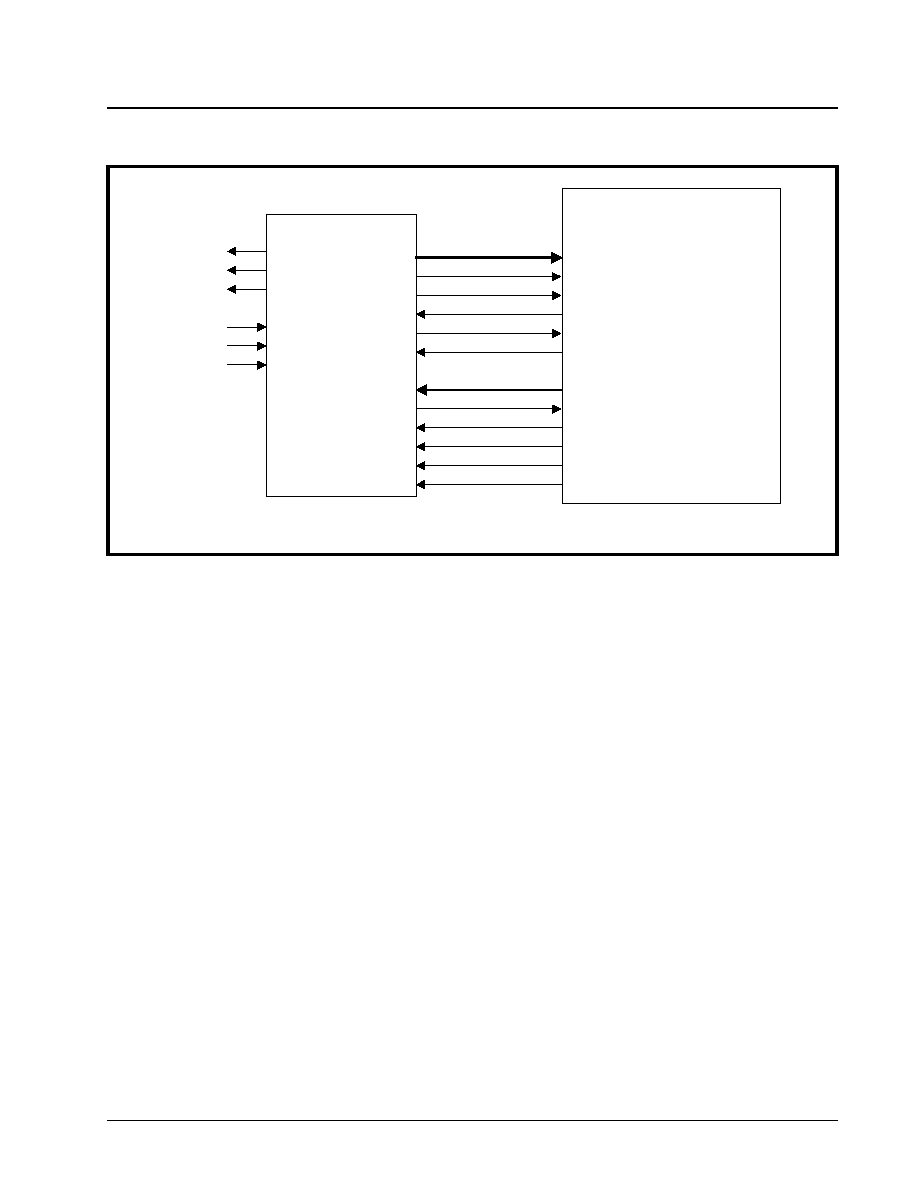
·Á
·Á
·Á
·Á
DS3 UNI FOR ATM
XRT7245
PRELIMINARY
REV. 1.03
279
This section presents a detailed description of "Single-
PHY" operation. Whenever the ATM Layer processor
is responsible for receiving cell data from the Receive
UTOPIA Interface block, it must do the following.
1.
Check the level of the RxClav pin
If the RxClav pin is "high" then the RxFIFO contains
some ATM cell data that needs to be read by the ATM
Layer processor. In this case, the ATM Layer proces-
sor should begin to read the cell data from the Receive
UTOPIA Interface block. However, if the RxClav pin is
"low", then the RxFIFO does not contain any cell data
that can be read. In this case, the ATM Layer proces-
sor should wait until RxClav toggles "high" before
attempting to read any more cell data from the
"Receive UTOPIA Interface block".
Note: The actual meaning associated with RxClav toggling
"high" or "low" depends upon whether the UNI is operating
in the "Cell Level" or "Octet Level" handshake modes.
2.
Assert the RxEnB* pin and read the first byte (or
word) of the new cell from the Receive UTOPIA
Data Bus.
Once the ATM Layer processor has detected that
RxClav has toggled "high", then it should assert the
RxEnB* input pin (e.g., toggling it "low"). Once the
Receive UTOPIA Interface block has determined that
the RxEnB* input pin is "low", then it will begin to
place some cell data onto the Receive UTOPIA Data
Bus. If this first byte (or word) is the beginning of a
new ATM cell, then the ATM Layer processor should
verify that this byte (or word) is indeed the beginning
of a new cell, by observing the RxSoC output pin (of
the UNI IC) pulsing "high" for one clock period of RxClk.
3.
Compute the odd-parity of the byte (or word) that
is being read from the Receive UTOPIA Data
bus, and compare the value of this parity bit with
that of the RxPrty output pin.
This operation is optional, but should be done concur-
rently while checking for the assertion of the RxSoc
output pin.
When reading in the subsequent bytes (or words) of
the cell, the ATM Layer must do the following.
∑
Repeat Steps 1 and 2.
∑
If the UNI is operating in the Octet-Level Hand-
shake mode, then the ATM Layer processor should
check the RxClav level prior to asserting the
RxEnB* (Receive UTOPIA Interface--Output Enable)
pin. The ATM Layer processor should only attempt
to read the contents of the Receive UTOPIA Data
Bus if the RxClav signal is "high".
∑
If the UNI is operating in the Cell-Level Handshake
mode, then the ATM Layer processor should check
the RxClav signal level just as it (the ATM Layer
processor) is reading in the very last byte (or word)
of a given cell. If the RxClav level is "high", then the
ATM Layer processor should proceed to read in the
next cell from the Receive UTOPIA Interface block.
F
IGURE
88. S
IMPLE
I
LLUSTRATION
OF
S
INGLE
-PHY O
PERATION
DS3 UNI
ATM Switch
(ATM Layer Device)
TxData[15:0]
RxData[15:0]
TxClav
TxPOS
TxNEG
RxPOS
RxNEG
Tx Flow Control Input
To/From
DS3 LIU
RxClav
TxSoC
TxEnB*
TxPrty
TxClk
RxClk
RxSoC
RxEnB*
RxPrty
Rx Flow Control Input
Rx Start of Cell Input
Tx Start of Cell Output
TxLineClk
RxLineClk
Rx Read Output Enable Signal
Tx Write Enable Output
Rx Utopia Data Bus Parity
Tx Utopia Data Bus Parity
Rx FIFO Clock Signal
Tx FIFO Clock Signal
Rx ATM Cell Data
Tx ATM Cell Data
XRT7245
DS3 UNI FOR ATM
·Á
·Á
·Á
·Á
PRELIMINARY
REV. 1.03
280
However, if the RxClav level is "low", then the ATM
Layer processor should halt reading in data, when
it reaches the end of the cell (that it is currently
reading in).
∑
The ATM Layer processor should keep a count on
the total number of bytes that have been read in
since the last assertion of the RxSoC output pin.
This will help the ATM Layer processor to determine
when it has reached the boundary of a given cell.
The previously-mentioned procedure is also depicted
in "Flow Chart Form" in Figure 89, and in Timing
Diagram form in Figure 90 and 91.
F
IGURE
89. F
LOW
C
HART
DEPICTING
THE
APPROACH
THAT
THE
ATM L
AYER
P
ROCESSOR
SHOULD
TAKE
WHEN
READING
CELL
DATA
FROM
THE
R
ECEIVE
UTOPIA I
NTERFACE
,
IN
THE
S
INGLE
-PHY M
ODE
.
START
Check the level of the RxClav pin.
Is
RxClav
"High"?
Is this
the first byte
(word) of a new
cell?
Is the
current Cell
Complete?
Is there
any more Cells
to read
?
END
Assert the Receive Utopia Interface block
Output Enable input pin - RxEnB*.
Read in the first byte (word) from the
Receive Utopia Data Bus.
Read in the odd-parity value of this byte/
word from the RxPry output pin.
Check and verify that the RxSoC pin is
asserted.
Perform the following, concurrently
READING IN THE FIRST BYTE/WORD
OF A CELL
Perform the following, concurrently
Read in the next byte (word) from the
Receive Utopia Data Bus
Read in the odd-parity value of this byte
(word) from the RxPry output pin.
Assert the "Receive Utopia Data Bus Output
Enable input pin - RxEnB*.
READING IN THE REMAINING
BYTES/WORDS OF A CELL
No
Yes
Yes
No
No
No
Yes
Yes
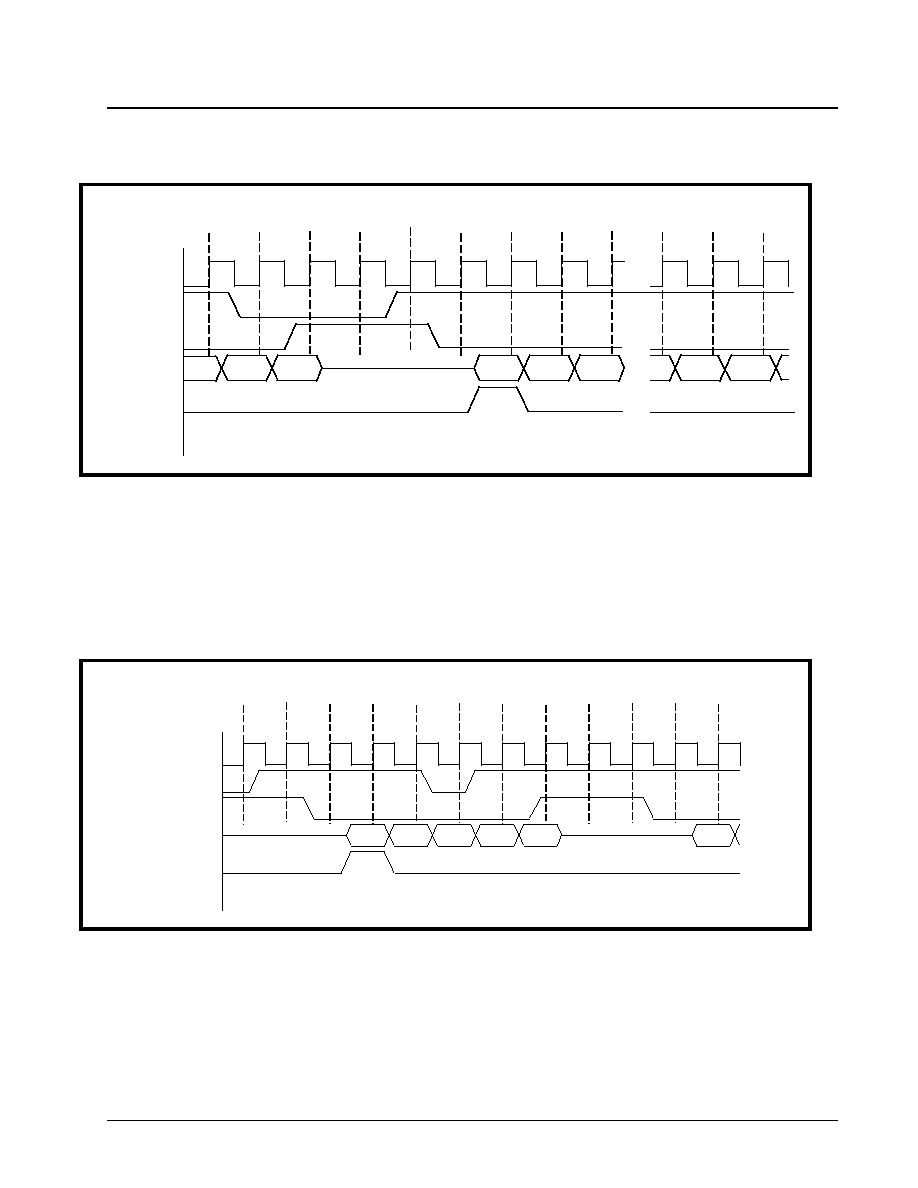
·Á
·Á
·Á
·Á
DS3 UNI FOR ATM
XRT7245
PRELIMINARY
REV. 1.03
281
Note: regarding Figure 90
1. The Receive UTOPIA Data bus is configured to be
16 bits wide. Hence, the data, which the Receive
UTOPIA Interface block places on the Receive
UTOPIA Data bus, is expressed in terms of 16-bit
words: (e.g., W0≠W26).
2. The Receive UTOPIA Data bus is configured to
handle 54 bytes/cell. Hence, Figure 90 illustrates
the ATM Layer processor reading 27 words (W0
through W26) for each ATM cell.
3. The Receive UTOPIA Interface block is configured
to operate in the Cell Level Handshake mode.
Note: regarding Figure 91
1. The Receive UTOPIA Data bus is configured to be
16 bits wide. Hence, the data, which the ATM Layer
processor places on the Transmit UTOPIA Data
bus, is expressed in terms of 16 bit words: (e.g.,
W0≠W26).
2. The Receive UTOPIA Interface block is configured
to handle 54 bytes/cell. Hence, Figure 91 illustrates
the ATM Layer processor reading 27 words (W0
through W26) for each ATM cell.
3. The Receive UTOPIA Interface block is configured
to operate in the Octet-Level Handshaking Mode.
F
IGURE
90. T
IMING
D
IAGRAM
OF
ATM L
AYER
PROCESSOR
R
ECEIVING
D
ATA
FROM
THE
UNI
OVER
THE
UTOPIA
D
ATA
B
US
, (S
INGLE
-PHY M
ODE
/C
ELL
L
EVEL
H
ANDSHAKING
).
RxClk
RxClav
RxEnB*
RxData[15:0]
RxSoC
W24
W25
W26
W0
W1
W2
W25
W26
1
2
3
4
5
6
7
8
9
31
32
34
F
IGURE
91. T
IMING
D
IAGRAM
OF
ATM L
AYER
PROCESSOR
R
ECEIVING
D
ATA
FROM
THE
UNI
OVER
THE
UTOPIA
D
ATA
B
US
, (S
INGLE
-PHY M
ODE
/O
CTET
L
EVEL
H
ANDSHAKING
).
RxClk
RxClav
RxEnB*
RxData[15:0]
RxSoC
W2
W3
W4
X
W1
W0
1
2
3
4
5
6
7
8
9
10
11
12
XRT7245
DS3 UNI FOR ATM
·Á
·Á
·Á
·Á
PRELIMINARY
REV. 1.03
282
Final Comments on Single-PHY Mode
The RxClav pin exhibits a role that is similar to the
"Ready Ready" function in RS-232 based data com-
munication. This pin is asserted when the RxFIFO
contains ATM cell data that can be read by the ATM
Layer processor. The RxClav pin will have a slightly
different role when the UNI is operating in the Multi-
PHY mode.
The UNI, while operating in Single-PHY mode, can
be configured for either "Octet-Level" or "Cell Level"
handshake modes. In either case, the ATM Layer
Processor is expected to poll the RxClav pin before
attempting to read in the next byte, word or cell from
the RxFIFO.
7.4.2.2.3.1
Multi-PHY Operation
The UNI IC will be operating in the Multi-PHY mode
upon power up or reset. In Multi PHY operating
mode, the ATM layer processor may be pumping data
into and reading data from several UNI devices in
parallel. When the UNI is operating in Multi-PHY mode,
the Receive UTOPIA Interface block will support two
kinds of operations with the ATM Layer processor.
∑
Polling for "available" UNI devices.
∑ Selecting which UNI (out of several possible UNI
devices) to read ATM cell data from.
Each of these operations are discussed in the sections
below. However, prior to discussing each of these
operations, the reader must understand the following.
"Multi-PHY" operation involves the use of one (1)
ATM Layer processor and several UNI devices, within
a system. The ATM Layer processor is expected to
read/write ATM cell data from/to these UNI devices.
Hence, "Multi-PHY" operation requires, at a minimum,
some means for the ATM Layer processor to uniquely
identify a UNI device (within the "Multi-PHY" system)
that it wishes to "poll", write ATM cell data to, or read
ATM cell data from. Actually, "Multi-PHY" operation
provides an addressing scheme that allows the ATM
Layer processor to uniquely identify "UTOPIA Interface
Blocks" (e.g., Transmit and Receive) within all of the
UNI devices, operating in the "Multi-PHY" system. In
order to uniquely identify a given "UTOPIA Interface
Block", within a "Multi-PHY" system, each "UTOPIA
Interface block" is assigned a 5-bit "UTOPIA Address"
value. The user assigns this address value to a par-
ticular "Receive UTOPIA Interface block" by writing
this address value into the "Rx UTOPIA Address
Register" (Address = 6Ch) within its "host" UNI
device. The bit-format of the "Rx UTOPIA Address
Register" is presented below.
Likewise, the user assigns a "UTOPIA address" value
to a particular "Transmit UTOPIA Interface block",
within one of the UNIs (in the "Multi-PHY" system) by
writing this address value into the "Tx UTOPIA
Address Register" (Address = 70h) within the "host"
UNI device. The bit-format of the "Tx UTOPIA
Address Register" is presented below.
Note: The role of the Transmit UTOPIA Interface block, in
"Multi-PHY" operation is presented in Section 6.1.2.3.2.
7.4.2.2.3.1.1
ATM Layer Processor "polling" of
the UNIs, in the Multi-PHY Mode
When the UNI is operating in the "Multi-PHY" mode,
the Receive UTOPIA Interface block will automatically
be configured to support "polling". "Polling" allows an
Receive UTOPIA Address Register: (Address = 6Ch)
B
IT
7
B
IT
6
B
IT
5
B
IT
4
B
IT
3
B
IT
2
B
IT
1
B
IT
0
Unused
Rx_UTOPIA_Addr[4:0]
RO
RO
RO
R/W
R/W
R/W
R/W
R/W
0
0
0
0
0
0
0
0
Tx UTOPIA Address Register (Address = 70h)
B
IT
7
B
IT
6
B
IT
5
B
IT
4
B
IT
3
B
IT
2
B
IT
1
B
IT
0
Unused
Tx_UTOPIA_Addr[4:0]
RO
RO
RO
R/W
R/W
R/W
R/W
R/W
0
0
0
0
0
0
0
0
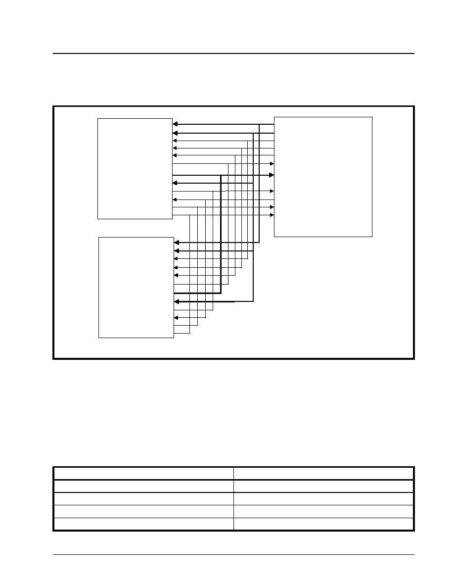
·Á
·Á
·Á
·Á
DS3 UNI FOR ATM
XRT7245
PRELIMINARY
REV. 1.03
283
ATM Layer processor (which is interface to several
UNI devices) to determine which UNIs contain ATM
cell data that needs to be read, at any given time.
The manner in which the ATM Layer processor "polls"
its UNI devices follows.
Figure 92 depicts a "Multi-PHY" system consisting of
an ATM Layer processor and two (2) UNI devices,
designated as "UNI #1" and "UNI #2". In this figure,
both of the UNIs are connected to the ATM Layer
processor via a common "Transmit UTOPIA" Data
Bus, "Receive UTOPIA" Data Bus, a common TxClav
line, a common RxClav line, as well as common
TxEnB*, RxEnB*, TxSoC and RxSoC lines. The ATM
Layer processor will also be addressing the Transmit
and Receive UTOPIA Interface block via a common
"UTOPIA" address bus (Ut_Addr[4:0]). Therefore, the
Transmit and Receive UTOPIA Blocks, of a given UNI
must have different addresses; as depicted in .
The UTOPIA Address values that have been assigned
to each of the Transmit and Receive UTOPIA Interface
blocks within Figure 91, are listed below in Table 63.
F
IGURE
92. A
N
I
LLUSTRATION
OF
M
ULTI
-PHY O
PERATION
WITH
UNI
DEVICES
#1
AND
#2
TxData[15:0]
TxAddr[4:0]
TxPrty
TxEnb*
TxSoC
TxClav
RxData[15:0]
RxAddr[4:0]
RxPrty
RxEnb*
RxSoC
RxClav
UNI # 1
TxAddr = 00h
RxAddr = 01h
TxData[15:0]
TxAddr[4:0]
TxPrty
TxEnb*
TxSoC
TxClav
RxData[15:0]
RxAddr[4:0]
RxPrty
RxEnb*
RxSoC
RxClav
TxAddr = 02h
RxAddr = 03h
TxData[15:0]
Ut_Addr[4:0]
Tx_Parity
Tx_Ut_WR*
Tx_SoC_out
TxClav_In
RxData[15:0]
Rx_Parity
Rx_Ut_Rd*
Rx_SoC_In
RxClav_In
ATM Layer Processor
UNI # 2
T
ABLE
63: UTOPIA A
DDRESS
VALUES
OF
THE
UTOPIA I
NTERFACE
B
LOCKS
ILLUSTRATED
IN
F
IGURE
92
B
LOCK
UTOPIA A
DDRESS
V
ALUE
Transmit UTOPIA Interface block--UNI #1
00h
Receive UTOPIA Interface block--UNI #1
01h
Transmit UTOPIA Interface block--UNI #2
02h
Receive UTOPIA Interface block--UNI #2
03h

XRT7245
DS3 UNI FOR ATM
·Á
·Á
·Á
·Á
PRELIMINARY
REV. 1.03
284
Recall, that the Receive UTOPIA Interface blocks were
assigned these addresses by writing these values into
the "Rx UTOPIA Address Register" (Address = 6Ch)
within their "host" UNI device. The discussion of the
Transmit UTOPIA Interface blocks, within UNIs #1
and #2 is presented in Section 6.1.2.3.2.1.
Polling Operation
Consider that the ATM Layer processor is currently
reading a continuous stream of cells from UNI #1.
While reading this cell data from UNI #1, the ATM
Layer processor can also "poll" UNI #2 for "availability"
(e.g., tries to determine if the RxFIFO within UNI #2,
contains some ATM cell data that needs to be read).
The ATM Layer Processor's Role in the "Polling"
Operation
The ATM Layer processor accomplishes this "polling"
operation by executing the following steps.
1.
Assert the RxEnB* input pin (if it not asserted
already).
The UNI device (being "polled") will know that this is
only a "polling" operation, if the RxEnB* input pin is
asserted, prior to detecting its UTOPIA Address on
the "UTOPIA Address" bus.
2.
The ATM Layer processor places the address of
the Receive UTOPIA Interface Block of UNI #2
onto the UTOPIA Address Bus, Ut_Addr[4:0],
3.
The ATM Layer processor will then check the
value of its "RxClav_in" input pin (see Figure 91).
The UNI Device's Role in the "Polling" Operation
UNI #2 will sample the signal levels placed on its
Rx UTOPIA Address input pins (RxAddr[4:0]) on the
rising edge of its "Receive UTOPIA Interface block"
clock input signal, RxClk. Afterwards, UNI #2 will com-
pare the value of these "Receive UTOPIA Address
Bus input pin" signals with that of the contents of its
"Rx UTOPIA Address Register" (Address = 6Ch).
If these values do not match (e.g., RxAddr[4:0] µ 03h)
then UNI #2 will keep its "RxClav" output signal "tri-
stated"; and will continue to sample its "Receive
UTOPIA Address bus input" pins, with each rising
edge of RxClk.
If these two values do match (e.g., RxAddr[4:0] = 03h)
then UNI #2 will drive its "RxClav" output pin to the
appropriate level, reflecting its RxFIFO "fill status".
Since the UNI is automatically operating in the "Cell
Level Handshaking" mode, while it is operating in the
"Multi-PHY" mode, the UNI will drive the RxClav out-
put signal "high" if it contains at least one complete
cell of data that needs to be read by the ATM Layer
processor. Conversely, the UNI will drive the "RxClav"
output signal "low" if its RxFIFO is depleted, or does
not contain at least one full cell of data.
When UNI #2 has been selected for "polling", UNI #1
will continue to keeps its "RxClav" output signal "tri-
stated". Therefore, when UNI #2 is driving its "RxClav"
output pin to the appropriate level; it will be driving
the entire "RxClav" line, within the "Multi-PHY" system.
Consequently, UNI#1 will also be driving the
"RxClav_in" input pin of the ATM Layer processor
(see Figure 92).
If UNI #2 drives the "RxClav" line "low", upon the
application of its address on the UTOPIA Address
bus, then the ATM Layer processor will "learn" that
UNI #2 does not contain any ATM cell data that is
ready to be read. However, if UNI #2 drives the Rx-
Clav line "high" (during "polling"), then the ATM Layer
processor will know that UNI#2 contains at least one
cell of data that needs to be read.
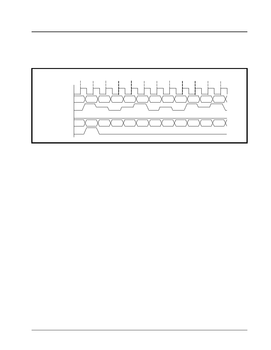
·Á
·Á
·Á
·Á
DS3 UNI FOR ATM
XRT7245
PRELIMINARY
REV. 1.03
285
Figure 93 presents a timing diagram, that depicts the
behavior of the ATM Layer processor's and the UNI's
signals during polling.
Note: regarding Figure 93
1. The Receive UTOPIA Data bus is configured to be
16 bits wide. Hence, the data, which the ATM Layer
processor places on the Receive UTOPIA Data
bus, is expressed in terms of 16 bit words: (e.g.,
W0≠W26).
2. The Receive UTOPIA Interface block is configured
to handle 54 bytes/cell. Hence, Figure 93 illustrates
the ATM Layer processor reading 27 words (W0
through W26) for each ATM cell.
3. The ATM Layer processor is currently reading ATM
cell data from the Receive UTOPIA Interface block,
within UNI #1 (RxAddr[4:0] = 01h) during this "polling
process".
4. The RxFIFO, within UNI#2's Receive UTOPIA
Interface block (RxAddr[4:0] = 03h) is either
depleted or does not contain enough data to con-
stitute a complete ATM cell. Hence, the RxClav line
will be driven "low" whenever this particular
Receive UTOPIA Interface block is "polled".
5. The Receive UTOPIA Address of 1Fh is not asso-
ciated with any UNI device, within this "Multi-PHY"
system. Hence, the RxClav line is tri-stated when-
ever this address is "polled".
Note: Although Figure 93 depicts connections between
the Transmit UTOPIA Interface block pins and the ATM
Layer processor; the Transmit UTOPIA Interface operation,
in the Multi-PHY mode, will not be discussed in this section.
Please see Section 6.1.2.3.2.1 for a discussion on the Trans-
mit UTOPIA Interface block during Multi-PHY operation.
7.4.2.2.3.1.2
Reading ATM Cell Data from
a Different UNI
After the ATM Layer processor has "polled" each of
the UNI devices within its system, it must now select
a UNI, and begin reading ATM cell data from that
device. The ATM Layer processor makes its selection
and begins the reading process by:
1.
Applying the UTOPIA Address of the "target" UNI
on the "UTOPIA Address Bus".
2.
Negate the RxEnB* signal. This step causes the
"addressed" UNI to recognize that it has been
selected to transmit the next set of ATM cell data
to the ATM Layer processor.
3.
Assert the RxEnB* signal.
4.
Check and insure that the RxSoC output pin (of
the selected UNI) pulses "high" when the first
byte or word of ATM cell data has been placed on
the Receive UTOPIA Data Bus.
5.
Begin reading the ATM Cell data in a byte-wide
(or word-wide) manner from the Receive UTOPIA
Data bus.
Figure 94 presents a flow-chart that depicts the "UNI
Device Selection and Read" process in Multi-PHY
operation.
F
IGURE
93. T
IMING
D
IAGRAM
ILLUSTRATING
THE
B
EHAVIOR
OF
VARIOUS
SIGNALS
FROM
THE
ATM L
AYER
PROCESSOR
AND
THE
UNI,
DURING
P
OLLING
.
RxClk
RxAddr[4:0]
RxClav
RxEnB*
RxData[15:0]
RxSoC
01h
1Fh
03h
1Fh
01h
03h
1Fh
03h
01h
1Fh
01h
03h
W27
W0
W1
W2
W3
W4
W5
W6
W7
W8
W9
W10
01h
03h
01h
03h
03h
01h
01h
1
2
3
4
5
6
7
8
9
10
11
12
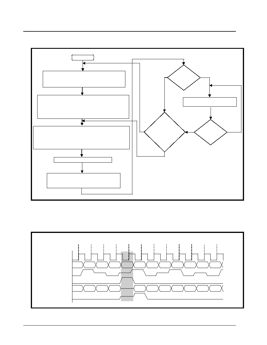
XRT7245
DS3 UNI FOR ATM
·Á
·Á
·Á
·Á
PRELIMINARY
REV. 1.03
286
Figure 95 presents a timing diagram that illustrates
the behavior of various "Receive UTOPIA Interface
block" signals, during the "Multi-PHY" UNI Device
Selection and Read operation.
F
IGURE
94. F
LOW
-C
HART
OF
THE
"UNI D
EVICE
S
ELECTION
AND
R
EAD
P
ROCEDURE
"
FOR
THE
M
ULTI
-PHY O
PERATION
.
START
Poll all UNIs within the "Multi-PHY" System
Determine which UNIs contain ATM cell data
that need to be read
Select "Availble" UNI
1. Apply Utopia Address of the "selected" Receive
Utopia Interface block onto the "Utopia Address"
bus
2. Negate the RxEnB* signal
Begin reading ATM cell data into "Selected" UNI
1. Assert RxEnB*
2. Read in the first byte/word of ATM cell from the
"Receive Utopia Data Bus & check for the asserted
RxSoC signal
Continue to read in ATM Cell data
Check the RxClav level while reading
in the last byte (word) of the current cell..
Is
RxClav
"High"
?
Wait for RxClav to toggle "high"
Is
RxClav
"High"
?
Does
the ATM
Layer processor
wish to read more
cells from the
"selected"
UNI?
Yes
No
Yes
Yes
No
No
F
IGURE
95. T
IMING
D
IAGRAM
OF
THE
R
ECEIVE
UTOPIA D
ATA
AND
A
DDRESS
B
US
SIGNALS
,
DURING
THE
"M
ULTI
-PHY"
UNI D
EVICE
S
ELECTION
AND
W
RITE
O
PERATIONS
.
RxClk
RxAddr[4:0]
RxClav
RxEnB*
RxData[15:0]
RxSoC
01h
1Fh
03h
1Fh
01h
03h
1Fh
01h
03h
1Fh
03h
01h
W0
W1
W2
W3
W4
W5
W6
W26
W25
W24
W23
Cell Received from 03h
Cell Received from 01h
01h
03h
01h
03h
01h
03h
03h
1
2
3
4
5
6
7
8
9
10
11
12
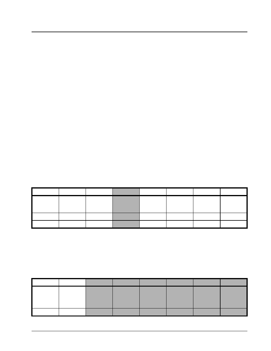
·Á
·Á
·Á
·Á
DS3 UNI FOR ATM
XRT7245
PRELIMINARY
REV. 1.03
287
Note: regarding Figure 95
1. The Receive UTOPIA Data bus is configured to be
16 bits wide. Hence, the data, which the Receive
UTOPIA Interface block places on the Receive
UTOPIA Data bus, is expressed in terms of 16-bit
words (e.g., W0≠W26).
2. The Receive UTOPIA Interface Block is configured
to handle 54 bytes/cell. Hence, Figure 95 illustrates
the ATM Layer processor reading 27 words (e.g.,
W0 through W26) for each ATM cell.
In Figure 95, the ATM Layer processor is initially
reading ATM cell data from the Receive UTOPIA
Interface within UNI #2 (RxAddr[4:0] = 03h). How-
ever, the ATM Layer processor is also polling the
Receive UTOPIA Interface block within UNI #1 (RxA-
ddr[4:0] = 01h) and some "non-existent" device at
RxAddr[4:0] = 1Fh. The ATM Layer processor com-
pletes its reading of the cell from UNI #1 at clock
edge #4. Afterwards, the ATM Layer will cease to
read any more cell data from UNI #1, and will begin
to read some cell data from UNI #2 (RxAddr[4:0] =
03h). The ATM Layer processor will indicates its
intention to select a new UNI device for reading by
negating the RxEnB* signal, at clock edge #5 (see
the shaded portion of Figure 95). At this time, UNI #1
will notice two things:
1.
The UTOPIA Address for the Receive UTOPIA
Interface block, within UNI #1 is on the Receive
UTOPIA Address bus (RxAddr[4:0] = 01h).
2.
The RxEnB* signal has been negated.
UNI #1 will interpret this signaling as an indication
that the ATM Layer processor is going to be perform-
ing read operations from it. Afterwards, the ATM
Layer processor will begin to read ATM cell data from
the Receive UTOPIA Interface block, within UNI #1.
7.4.2.3
Receive UTOPIA Interrupt Servicing
The Receive UTOPIA Interface block will generate
interrupts upon the following conditions:
∑
Change of Cell Alignment (e.g., the detection of
"runt" cells)
∑
Rx FIFO Overrun
∑ Rx FIFO Underrun
If one of these conditions occur and if that particular
condition is enabled for interrupt generation, then
when the local µP/µC reads the UNI Interrupt status
register, as shown below, it should read "xxx1xxxxb"
(where the -b suffix denotes a binary expression, and
the -x denotes a "don't care" value).
At this point, the local µC/µP has determined that the
Receive UTOPIA Interface block is the source of the
interrupt, and that the Interrupt Service Routine
should branch accordingly.
The next step in the interrupt service routine should be
to determine which of the three Receive UTOPIA
Block interrupt conditions has occurred and is causing
the Interrupt. In order to accomplish this, the local
µP/µC should now read the "Rx UT Interrupt Enable/
Status Register, which is located at address 6Bh in
the UNI device. The bit format of this register is
presented below.
UNI Interrupt Status Register (Address = 05h)
B
IT
7
B
IT
6
B
IT
5
B
IT
4
B
IT
3
B
IT
2
B
IT
1
B
IT
0
Rx DS3
Interrupt
Status
Rx PLCP
Interrupt
Status
Rx CP
Interrupt
Status
Rx UTOPIA
Interrupt
Status
Tx UTOPIA
Interrupt
Status
Tx CP
Interrupt
Status
Tx DS3
Interrupt
Status
One Sec
Interrupt
Status
RO
RO
RO
RO
RO
RO
RO
RUR
x
x
x
x
1
x
x
x
Address = 6Bh, Rx UT Interrupt Enable/Status Register
B
IT
7
B
IT
6
B
IT
5
B
IT
4
B
IT
3
B
IT
2
B
IT
1
B
IT
0
Unused
RxFIFO
Reset
RxFIFO
Overflw
Interrupt
Enable
RxFIFO
Underflw
Interrupt
Enable
RCOCA
Interrupt
Enable
RxFIFO
Overflw
Interrupt
Status
RxFIFO
Underflw
Interrupt
Status
RCOCA
Interrupt
Status
RO
R/W
R/W
R/W
R/W
RUR
RUR
RUR
XRT7245
DS3 UNI FOR ATM
·Á
·Á
·Á
·Á
PRELIMINARY
REV. 1.03
288
The Rx UT Interrupt Enable/Status Register has
eight bit-fields. However, only six of these bit-fields
are relevant to interrupt processing. Bits 0≠2 are the
interrupt status bits and bits 3≠5 are the interrupt en-
able bits for the Receive UTOPIA Interface block.
Each of these "interrupt processing relevant" bit-
fields are defined below.
Bit 0≠--RCOCA Interrupt Status--Receive UTOPIA
Change of Cell Alignment Condition
If the RxFIFO Manager detects a "runt" cell, then it
will generate the "Receive UTOPIA Change of Cell
Alignment Condition" interrupt, and the "runt" cell will
be discarded. The Receive UTOPIA Interface block
will indicate that it is generating this kind of interrupt
by asserting Bit 0 (RCOCA Interrupt Status) of the
Receive UTOPIA Interrupt Enable/Status Register,
as depicted below.
Bit 1--Rx FIFO Underflw Interupt Status--RxFIFO
Underrun Condition
Whenever the Receive UTOPIA Interface block sets
its RxClav signal to "high", the ATM Layer processor
will know that the RxFIFO has some ATM cell data
that needs to be read. Hence, the ATM Layer processor
will begin to read out this cell data. If the ATM Layer
processor reads out all of the cell data and depletes
the RxFIFO, then the UNI will generate an "RxFIFO
Underrun" Interrupt. The Receive UTOPIA Interface
block will indicate that it is generating this kind of
interrupt by asserting Bit 1 (RxFIFO Underflw Inter-
rupt Status) of the Receive UTOPIAn Interrupt
Enable/Status Register, as depicted below.
Bit 2--Rx FIFO Overflw Interrupt Status--RxFIFO
Overrun Condition
If the RxFIFO is filled to capacity, and if the ATM Layer
processor is unable to begin reading its contents
before the Receive Cell Processor writes another cell
into the RxFIFO, some of the data within the RxFIFO
will be overwritten, and in turn lost. If the Receive
UTOPIA Interface block detects this condition, and if
this interrupt condition has been enabled then the
UNI will assert the INT* pin to the local µP/µC. Addi-
tionally, the UNI will set bit 2, within the Receive
UTOPIA Interrupt Enable/Status Register to "1" as
depicted below.
Address = 6Bh, Rx UT Interrupt Enable/Status Register
B
IT
7
B
IT
6
B
IT
5
B
IT
4
B
IT
3
B
IT
2
B
IT
1
B
IT
0
Unused
RxFIFO
Reset
RxFIFO
Overflw
Interrupt
Enable
RxFIFO
Underflw
Interrupt
Enable
RCOCA
Interrupt
Enable
RxFIFO
Overflw
Interrupt
Status
RxFIFO
Underflw
Interrupt
Status
RCOCA
Interrupt
Status
RO
R/W
R/W
R/W
R/W
RUR
RUR
RUR
0
0
x
x
1
x
x
1
Address = 6Bh, Rx UT Interrupt Enable/Status Register
B
IT
7
B
IT
6
B
IT
5
B
IT
4
B
IT
3
B
IT
2
B
IT
1
B
IT
0
Unused
RxFIFO
Reset
RxFIFO
Overflw
Interrupt
Enable
RxFIFO
Underflw
Interrupt
Enable
RCOCA
Interrupt
Enable
RxFIFO
Overflw
Interrupt
Status
RxFIFO
Underflw
Interrupt
Status
RCOCA
Interrupt
Status
RO
R/W
R/W
R/W
R/W
RUR
RUR
RUR
0
0
x
1
x
x
1
x
·Á
·Á
·Á
·Á
DS3 UNI FOR ATM
XRT7245
PRELIMINARY
REV. 1.03
289
Bit 3--RCOCA Interrupt Enable--Receive UTOPIA
Change of Cell Alignment Interrupt Enable
This "Read/Write" bit-field allows the user to enable or
disables the generation of interrupts due to a detect-
ed "Change of Cell Alignment" condition, within the
RxFIFO. The local µP/µC can enable this interrupt by
writing a "1" to this bit-field. Upon power up or reset
conditions, this bit-field will contain a "0". Therefore
the default condition is for this interrupt to be disabled.
Bit 4--RxFIFO Underflw Interrupt Enable--
Rx FIFO Underrun Condition Interrupt Enable
This "Read/Write" bit-field allows the user to enable
or disable the generation of interrupts due to an "Rx
FIFO Underrun" condition. The local µP/µC can enable
this interrupt by writing a "1" to this bit-field. Upon
power up or reset conditions, this bit-field will contain
a "0". Therefore, the default condition is for this inter-
rupt to be disabled.
Bit 5--RxFIFO Overflw Interrupt Enable--Rx FIFO
Overrun Condition Interrupt Enable
This "Read/Write" bit-field allows the user to enable
or disable the generation of interrupts due to an "Rx
FIFO Overrun" condition. The local µP/µC can enable
this interrupt by writing a "1" to this bit-field. Upon
power up or reset conditions, this bit-field will contain
a "0". Therefore, the default condition is for this inter-
rupt to be disabled.
Address = 6Bh, Rx UT Interrupt Enable/Status Register
B
IT
7
B
IT
6
B
IT
5
B
IT
4
B
IT
3
B
IT
2
B
IT
1
B
IT
0
Unused
RxFIFO
Reset
RxFIFO
Overflw
Interrupt
Enable
RxFIFO
Underflw
Interrupt
Enable
RCOCA
Interrupt
Enable
RxFIFO
Overflw
Interrupt
Status
RxFIFO
Underflw
Interrupt
Status
RCOCA
Interrupt
Status
RO
R/W
R/W
R/W
R/W
RUR
RUR
RUR
0
0
1
x
x
1
x
x

XRT7245
DS3 UNI FOR ATM
·Á
·Á
·Á
·Á
PRELIMINARY
REV. 1.03
290
8.0 TIMING DIAGRAMS
F
IGURE
96. XRT7245 T
RANSMIT
UTOPIA I
NTERFACE
B
LOCK
T
IMING
TxData[15:0]
TxEn*
TxPrty
TxSoC
TxAddr[4:0]
TxClav
TxClk
t1
t3
t2
t5
t7
t6
t8
t4
t9
t10
t11
t12
F
IGURE
97. GFC N
IBBLE
-F
IELD
S
ERIAL
I
NPUT
I
NTERFACE
(
AT
T
RANSMIT
C
ELL
P
ROCESSOR
) T
IMING
TxGFCClk
TxGFCMSB
t14
TxGFC
t16
BIT 3
BIT 2
BIT 1
BIT 0
t17
t13
t15
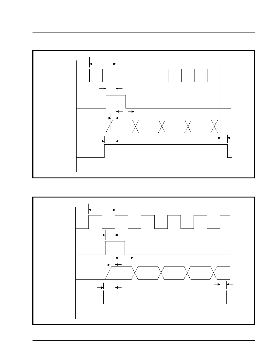
·Á
·Á
·Á
·Á
DS3 UNI FOR ATM
XRT7245
PRELIMINARY
REV. 1.03
291
F
IGURE
98. T
RANSMIT
PLCP P
ROCESSOR
--POH B
YTE
S
ERIAL
I
NPUT
P
ORT
I
NTERFACE
T
IMING
TxPOHFrame
TxPOH
TxPOHIns
TxPOHClk
t19
t20
t21
t23
t22
t18
F
IGURE
99. T
RANSMIT
DS3 F
RAMER
--OH B
IT
S
ERIAL
I
NPUT
P
ORT
I
NTERFACE
T
IMING
TxOHFrame
TxOH
TxOHIns
TxOHClk
t25
t26
t27
t29
t28
t24
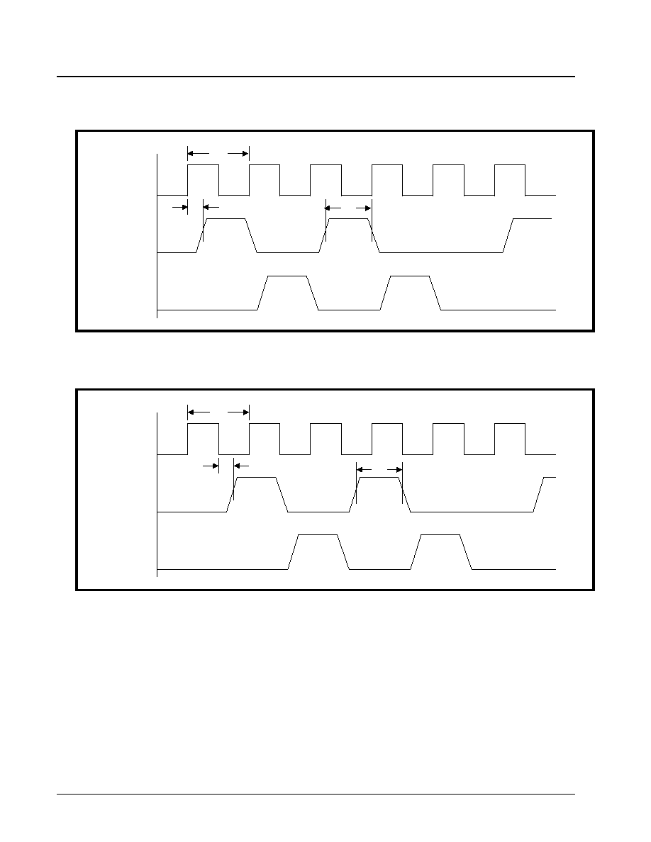
XRT7245
DS3 UNI FOR ATM
·Á
·Á
·Á
·Á
PRELIMINARY
REV. 1.03
292
F
IGURE
100. T
RANSMIT
DS3 F
RAMER
L
INE
I
NTERFACE
O
UTPUT
T
IMING
(T
X
POS
AND
T
X
NEG
ARE
UPDATED
ON
THE
RISING
EDGE
OF
T
X
L
INE
C
LK
)
F
IGURE
101. T
RANSMIT
DS3 F
RAMER
L
INE
I
NTERFACE
O
UTPUT
T
IMING
(T
X
POS
AND
T
X
NEG
ARE
UPDATED
ON
THE
FALLING
EDGE
OF
T
X
L
INE
C
LK
)
TxLineClk
TxPOS
TxNEG
t32
t30
t33
TxLineClk
TxPOS
TxNEG
t31
t32
t33
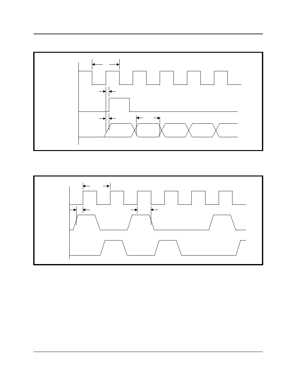
·Á
·Á
·Á
·Á
DS3 UNI FOR ATM
XRT7245
PRELIMINARY
REV. 1.03
293
F
IGURE
102. R
ECEIVE
DS3 F
RAMER
--OH B
IT
S
ERIAL
O
UTPUT
P
ORT
I
NTERFACE
T
IMING
RxOHFrame
RxOHClk
RxOH
t35
t36
t37
t34
F1
X1
F1
AIC
F0
F
IGURE
103. R
ECEIVE
DS3 F
RAMER
L
INE
I
NTERFACE
I
NPUT
S
IGNAL
T
IMING
(R
X
POS
AND
R
X
NEG
ARE
SAMPLED
ON
RISING
EDGE
OF
R
X
L
INE
C
LK
)
RxLineClk
RxPOS
RxNEG
t38
t39
t42
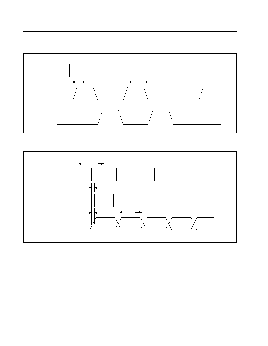
XRT7245
DS3 UNI FOR ATM
·Á
·Á
·Á
·Á
PRELIMINARY
REV. 1.03
294
F
IGURE
104. R
ECEIVE
DS3 F
RAMER
L
INE
I
NTERFACE
I
NPUT
S
IGNAL
T
IMING
(R
X
POS
AND
R
X
NEG
ARE
SAMPLED
ON
THE
FALLING
EDGE
OF
R
X
L
INE
C
LK
)
RxLineClk
RxPOS
RxNEG
t40
t41
F
IGURE
105. R
ECEIVE
PLCP P
ROCESSOR
--POH B
YTE
S
ERIAL
O
UTPUT
P
ORT
I
NTERFACE
T
IMING
RxPOHFrame
RxPOHClk
RxPOH
t44
t45
t46
t43
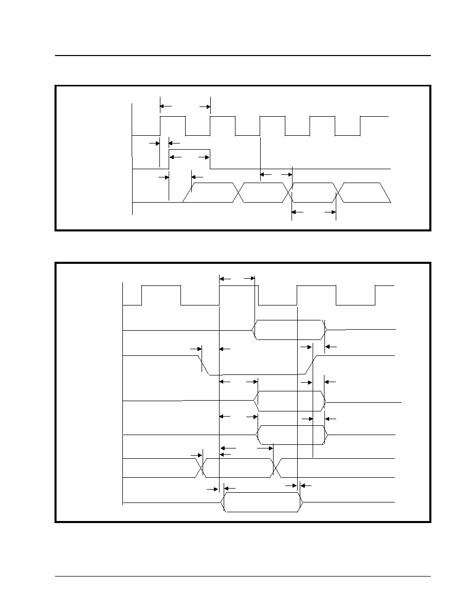
·Á
·Á
·Á
·Á
DS3 UNI FOR ATM
XRT7245
PRELIMINARY
REV. 1.03
295
F
IGURE
106. GFC N
IBBLE
-F
IELD
S
ERIAL
O
UTPUT
P
ORT
T
IMING
(R
ECEIVE
C
ELL
P
ROCESSOR
)
RxGFCClk
RxGFCMSB
t52
RxGFC
BIT 3
BIT 2
BIT 1
BIT 0
t50
t48
t51
t47
t49
F
IGURE
107. R
ECEIVE
UTOPIA I
NTERFACE
B
LOCK
T
IMING
RxData[15:0]
RxEn*
RxPrty
RxSoC
RxAddr[4:0]
RxClav
RxClk
t54
t57
t60
t61
t62
t63
t53
DATA VALID
t55
t58
t59
VALID ADDRESS
ADDRESS of ANOTHER UNI
ADDRESS of ANOTHER UNI
t56
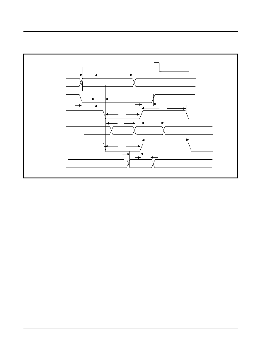
XRT7245
DS3 UNI FOR ATM
·Á
·Á
·Á
·Á
PRELIMINARY
REV. 1.03
296
F
IGURE
108. M
ICROPROCESSOR
I
NTERFACE
T
IMING
--R
EAD
AND
W
RITE
O
PERATIONS
, I
NTEL
T
YPE
P
ROCESSORS
,
N
ON
-B
URST
M
ODE
A8 - A0
CS*
WRB_RW
(WR*)
D15 - D0
(Read)
FLOAT
NOT
VALID
VALID
FLOAT
D15 - D0
(Write)
VALID
t64
t66
t65
t67
t74
t72
t73
t70
t74
t71
RDB_DS
(RD*)
t69
ALE_AS
(ALE)
t68
t69
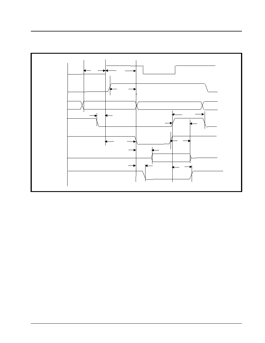
·Á
·Á
·Á
·Á
DS3 UNI FOR ATM
XRT7245
PRELIMINARY
REV. 1.03
297
F
IGURE
109. M
ICROPROCESSOR
I
NTERFACE
T
IMING
--M
OTOROLA
T
YPE
P
ROCESSORS
(R
EAD
O
PERATIONS
)
N
ON
-B
URST
M
ODE
WRB_RW
(R/W*)
CS*
ALE_AS
(AS*)
RDB_DS
(DS*)
D15 - D0
VALID DATA
A8 - A0
ADDRESS BEING READ
t75
t76
t77
t78
t83
t84
t80
t82
t79
Rdy_Dtck
(DTACK*)
t81
t85
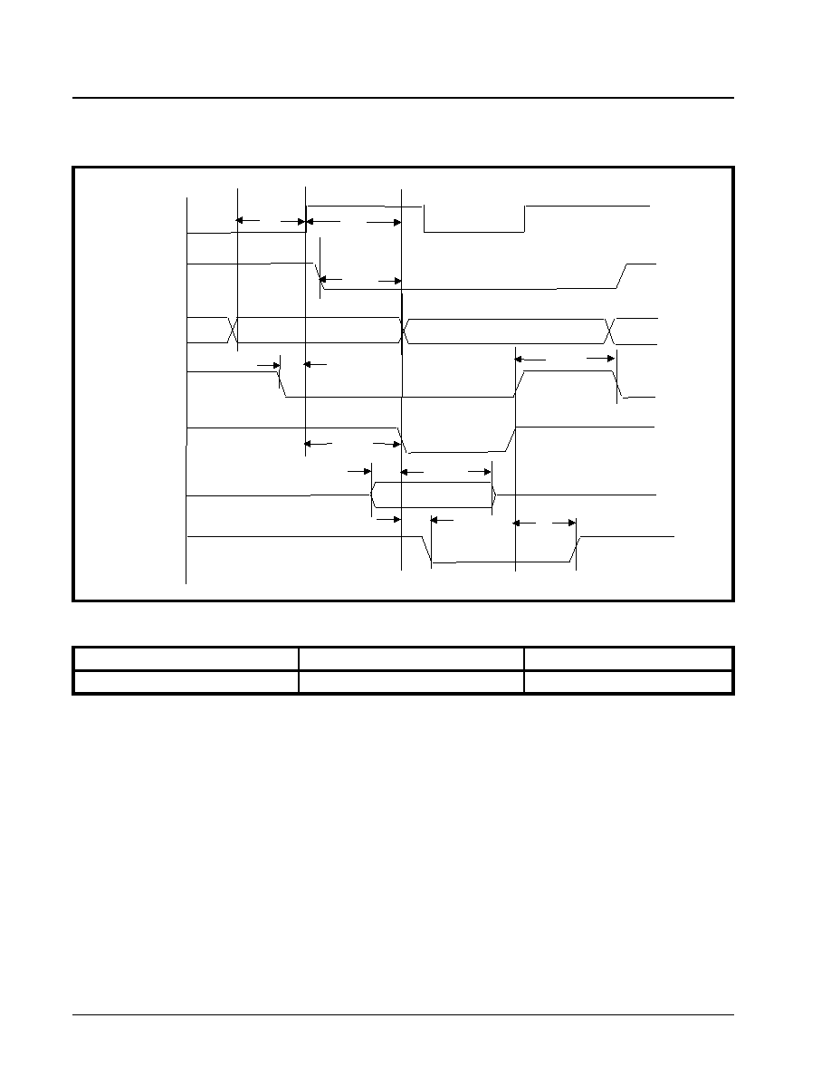
XRT7245
DS3 UNI FOR ATM
·Á
·Á
·Á
·Á
PRELIMINARY
REV. 1.03
298
ORDERING INFORMATION
F
IGURE
110. M
ICROPROCESSOR
I
NTERFACE
T
IMING
--M
OTOROLA
T
YPE
P
ROCESSOR
(W
RITE
O
PERATIONS
)
N
ON
-B
URST
M
ODE
WRB_RW
(R/W*)
CS*
ALE_AS
(AS*)
RDB_DS
(DS*)
D15 - D0
VALID DATA
A8 - A0
ADDRESS BEING WRITTEN TO
t75
t76
t77
t86
t87
t82
t79
Rdy_Dtck
(DTACK*)
t81
t85
t88
P
ART
N
UMBER
P
ACKAGE
O
PERATING
T
EMPERATURE
R
ANGE
XRT7245SIQ160
28 x28 mm Plastic QFP
-40∞C to +85∞C
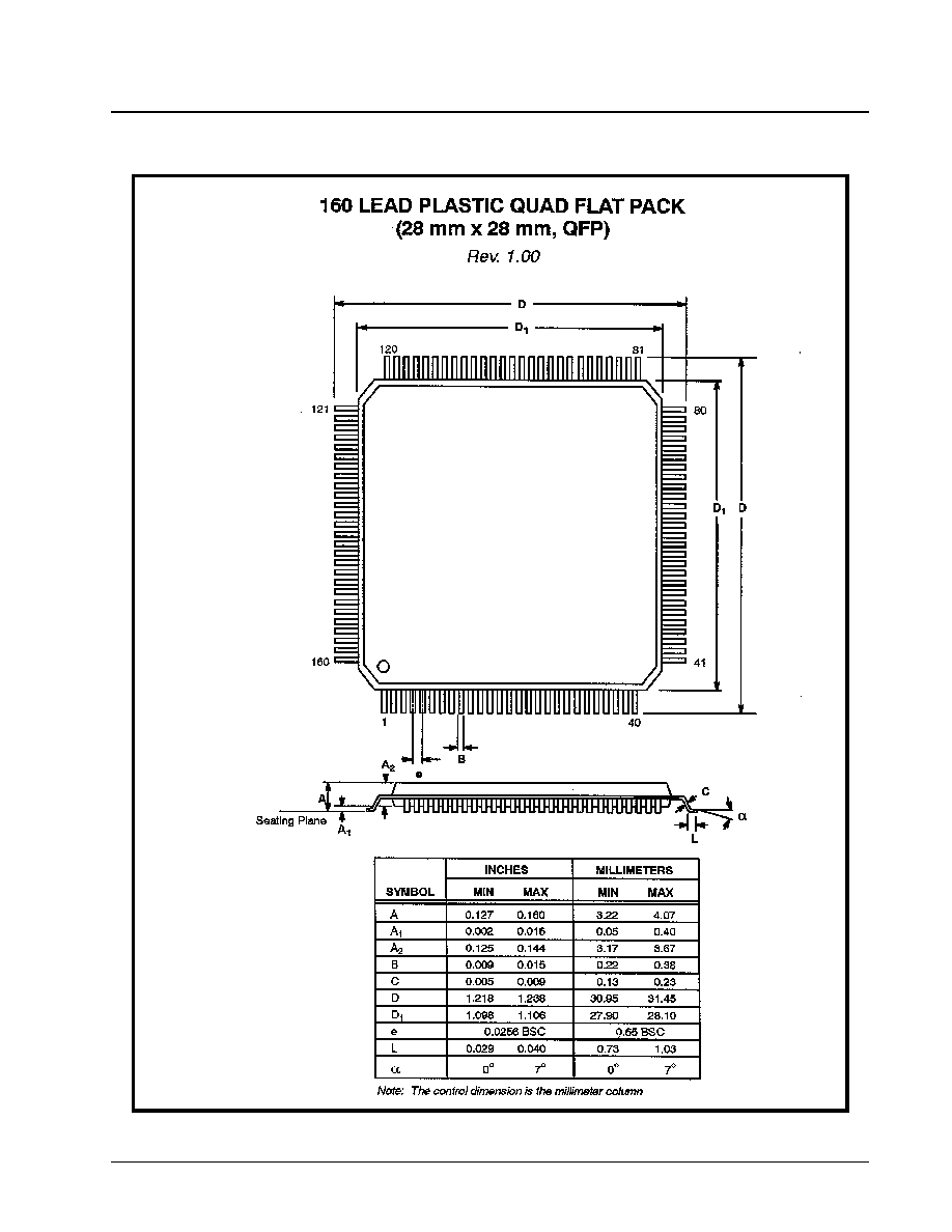
·Á
·Á
·Á
·Á
DS3 UNI FOR ATM
XRT7245
PRELIMINARY
REV. 1.03
299
PACKAGE DIMENSIONS

·Á
·Á
·Á
·Á
XRT7245 DS3 UNI FOR ATM
PRELIMINARY
REV. 1.03
300
NOTICE
EXAR Corporation reserves the right to make changes to the products contained in this publication in order to
improve design, performance or reliability. EXAR Corporation assumes no responsibility for the use of any cir-
cuits described herein, conveys no license under any patent or other right, and makes no representation that
the circuits are free of patent infringement. Charts and schedules contained here in are only for illustration pur-
poses and may vary depending upon a user's specific application. While the information in this publication has
been carefully checked; no responsibility, however, is assumed for inaccuracies.
EXAR Corporation does not recommend the use of any of its products in life support applications where the
failure or malfunction of the product can reasonably be expected to cause failure of the life support system or to
significantly affect its safety or effectiveness. Products are not authorized for use in such applications unless
EXAR Corporation receives, in writing, assurances to its satisfaction that: (a) the risk of injury or damage has
been minimized; (b) the user assumes all such risks; (c) potential liability of EXAR Corporation is adequately
protected under the circumstances.
Copyright 1999 EXAR Corporation
Datasheet December 1999
Reproduction, in part or whole, without the prior written consent of EXAR Corporation is prohibited.

·Á
·Á
·Á
·Á
DS3 UNI FOR ATM
XRT7245
PRELIMINARY
REV. 1.03
I
TABLE OF CONTENTS
GENERAL DESCRIPTION .................................................................................................................1
Features ............................................................................................................................................................ 1
Applications ..................................................................................................................................................... 1
Ordering Information ............................................................................................................................2
Functional Description .................................................................................................................................... 3
The Receive Section ........................................................................................................................................ 3
The Transmit Section ...................................................................................................................................... 3
The Microprocessor Interface Section .......................................................................................................... 4
Performance Monitor Section ........................................................................................................................ 4
Test and Diagnostic Section .......................................................................................................................... 4
Line Interface Drive and Scan Section .......................................................................................................... 5
FEATURES ....................................................................................................................................................... 6
Transmit and Receive Sections ..................................................................................................................... 6
UTOPIA Interface Blocks ................................................................................................................................... 6
Transmit Cell Processor Block .......................................................................................................................... 7
Receive Cell Processor Block ........................................................................................................................... 7
Transmit PLCP Processor Block ....................................................................................................................... 7
Receive PLCP Processor Block ........................................................................................................................ 7
Transmit/Receive DS3 Framer Block ................................................................................................................ 7
Microprocessor Interface Section ...................................................................................................................... 7
Performance Monitor Section ............................................................................................................................ 8
Test and Diagnostic Section .............................................................................................................................. 8
Line Interface Drive and Scan Section .............................................................................................................. 8
PIN DESCRIPTION ........................................................................................................................................... 9
Absolute Maximum Ratings ...............................................................................................................26
DC ELECTRICAL CHARACTERISTICS ........................................................................................26
AC ELECTRICAL CHARACTERISTICS ........................................................................................26
1.0 SYSTEM DESCRIPTION ........................................................................................... 32
System Level Interfacing of the XRT7245 DS3 UNI ....................................................... 32
Interfacing to the ATM Switch (ATM Layer Processor) .............................................................................. 32
Interfacing to the Local Microprocessor ..................................................................................................... 32
Interfacing the UNI to the DS3 Line ............................................................................................................. 32
Internal Operation of the XRT7245 DS3 UNI device ....................................................... 34
PRINCIPLE OF OPERATION ..........................................................................................................36
2.0 THE USER NETWORK INTERFACE (UNI) ............................................................... 36
3.0 MICROPROCESSOR INTERFACE SECTION AND ON-CHIP PROGRAMMABLE
REGISTERS 38
The Microprocessor Interface Signals ............................................................................ 38
Interfacing the XRT7245 DS3 UNI to the Local µC/µP Over Via the Microprocessor In-
terface Block ..................................................................................................................... 40

XRT7245
DS3 UNI FOR ATM
·Á
·Á
·Á
·Á
PRELIMINARY
REV. 1.03
II
Reading Performance Monitor (PMON) Registers ...................................................................................... 41
For Example ..................................................................................................................................................... 41
The PMON Holding Register ........................................................................................................................... 41
In Summary: Whenever an "8-bit" µC/µP needs to read a PMON Register, it must execute the following steps.
41
On-Chip Register Organization ....................................................................................... 54
Address = 00h, UNI Operating Mode Register ............................................................................................ 59
Bit 7--Line Loop Back Mode ........................................................................................................................ 60
Bit 6--Cell Loop Back Mode .........................................................................................................................60
Bit 5--PLCP Loop Back Mode ...................................................................................................................... 60
Bit 4--Reset .................................................................................................................................................... 60
Bit 3--Direct Mapped ATM/PLCP Mode* Selection ..................................................................................... 60
Bit 2--M13/C-Bit* (DS3 Frame Format) Selection ....................................................................................... 60
Bits 1, 0--TimRefSel[1, 0] (Timing Reference Select--Transmit PLCP Processor and Transmit DS3 Fram-
er) .................................................................................................................................................................... 60
Address = 01h, UNI I/O Control Register ..................................................................................................... 61
Bit 7--LOC (Loss of Clock)Enable ............................................................................................................... 61
Bit 6--Test PMON .......................................................................................................................................... 61
Bit 5--Int En Reset (Automatic Reset of Interrupt Enable Bits) Select ..................................................... 61
Bit 4--AMI/B3ZS* (Line Code) ....................................................................................................................... 62
Bit 3--Unipolar/Bipolar* (Line Code) ............................................................................................................62
Bit 2--TxLineClk Inv ...................................................................................................................................... 62
Bit 1--RxLineClk Inv ...................................................................................................................................... 62
Bit 0--Reframe (Receive DS3 Framer) ......................................................................................................... 62
Address = 02h, Part Number Register ......................................................................................................... 62
Address = 03h, Version Number Register ................................................................................................... 63
Address = 04h, UNI Interrupt Enable Register ............................................................................................ 63
Bit 7--Rx DS3 Interrupt Enable .................................................................................................................... 63
Bit 6--Rx PLCP Interrupt Enable .................................................................................................................. 63
Bit 5--Rx CP Interrupt Enable ...................................................................................................................... 63
Bit 4--Rx UTOPIA Interrupt Enable .............................................................................................................. 63
Bit 3--Tx UTOPIA Interrupt Enable .............................................................................................................. 64
Bit 2--Tx CP Interrupt Enable ....................................................................................................................... 64
Bit 1--Tx DS3 Framer Interrupt Enable ........................................................................................................ 64
Bit 0--One Second Interrupt Enable ............................................................................................................64
Address = 05h, UNI Interrupt Status Register ............................................................................................. 64
Bit 7--Rx DS3 (Framer) Interrupt Status ......................................................................................................64
Bit 6--Rx PLCP Interrupt Status ...................................................................................................................65
Bit 5--Rx CP (Cell Processor) Interrupt Status ........................................................................................... 65
Bit 4--Rx UTOPIA Interrupt Status ............................................................................................................... 65
Bit 3--Tx UTOPIA Interrupt Status ............................................................................................................... 65
Bit 2--Tx CP (Cell Processor) Interrupt Status ........................................................................................... 65
Bit 1--Tx DS3 (Framer) Interrupt Status ......................................................................................................65
Bit 0--One Second Interrupt Status ............................................................................................................. 66

·Á
·Á
·Á
·Á
DS3 UNI FOR ATM
XRT7245
PRELIMINARY
REV. 1.03
III
Address = 06h, Test Cell Control and Status Register .............................................................................. 66
Bit 4--Test Cell (Generator/Receiver) Enable ............................................................................................. 66
Bit 3--Line*/System (Side Testing) .............................................................................................................. 66
Bit 2--One Shot Test ..................................................................................................................................... 66
Bit 1--One Shot Done ................................................................................................................................... 67
Bit 0--PRBS (Pseudo-Random Byte Sequence) Lock ............................................................................... 67
Address = 07h, Future Use ........................................................................................................................... 67
Address = 08h, Test Cell Header Byte-1 ...................................................................................................... 67
Address = 09h, Test Cell Header Byte-2 ...................................................................................................... 67
Address = 0Ah, Test Cell Header Byte-3 ..................................................................................................... 68
Address = 0Bh, Test Cell Header Byte-4 ..................................................................................................... 68
Address = 0Ch, Test Cell Error Accumulator--MSB .................................................................................. 68
Address = 0Dh, Test Cell Error Accumulator--LSB ................................................................................... 69
Address = 0Eh, Rx DS3 Configuration and Status Register ...................................................................... 69
Bit 7--RxAIS--Receive AIS Signal ............................................................................................................... 69
Bit 6--RxLOS--Receive LOS Condition ...................................................................................................... 69
Bit 5--RxIdle--Receive Idle Condition ........................................................................................................ 69
Bit 4--RxOOF--Out of Frame Condition ..................................................................................................... 69
Bit 3--Int (Receive DS3 Framer) LOS Disable ............................................................................................ 69
Bit 2--Framing On Parity .............................................................................................................................. 69
Bit 1--FSync Algo ......................................................................................................................................... 70
Bit 0--MSync Algo ......................................................................................................................................... 70
Address = 0Fh, Rx DS3 Status Register ...................................................................................................... 70
Bit 4--RxFERF (Far End Receive Failure) ................................................................................................... 70
Bit 3--RxAIC .................................................................................................................................................. 70
Bits 2-0 RxFEBE[2:0] ..................................................................................................................................... 70
Address = 10h, Rx DS3 Interrupt Enable Register ..................................................................................... 71
Bit 7--CP Bit Error Interrupt Enable ............................................................................................................ 71
Bit 6--LOS Interrupt Enable ......................................................................................................................... 71
Bit 5--AIS Interrupt Enable ........................................................................................................................... 71
Bit 4--Idle (Condition) Interrupt Enable ...................................................................................................... 71
Bit 3--FERF Interrupt Enable ....................................................................................................................... 71
Bit 2--AIC Interrupt Enable .......................................................................................................................... 71
Bit 1--OOF Interrupt Enable ......................................................................................................................... 71
Bit 0--Parity Error Interrupt Enable ............................................................................................................. 71
Address = 11h, RxDS3 Interrupt Status Register ....................................................................................... 72
Bit 7--CP Bit Error Interrupt Status ............................................................................................................. 72
Bit 6--LOS Interrupt Status .......................................................................................................................... 72
Bit 5--AIS Interrupt Status ........................................................................................................................... 72
Bit 4--Idle Interrupt Status ........................................................................................................................... 72
Bit 3--FERF Interrupt Status ........................................................................................................................ 72
Bit 2--(Change in) AIC Interrupt Status ...................................................................................................... 73
Bit 1--OOF (Receive DS3 Framer) Interrupt Status ................................................................................... 73
Bit 0--P-Bit Error (Receive DS3 Framer) Interrupt Status ......................................................................... 73

XRT7245
DS3 UNI FOR ATM
·Á
·Á
·Á
·Á
PRELIMINARY
REV. 1.03
IV
Address = 12h, RxDS3 FEAC Register ......................................................................................................... 73
Address = 13h, RxDS3 FEAC Interrupt Enable/Status Register ................................................................ 73
Bit 4--FEAC Valid .......................................................................................................................................... 73
Bit 3--RxFEAC Remove Interrupt Enable .................................................................................................... 74
Bit 2--RxFEAC Remove Interrupt Status ..................................................................................................... 74
Bit 1--RxFEAC Valid Interrupt Enable ......................................................................................................... 74
Bit 0--RxFEAC Valid Interrupt Status .......................................................................................................... 74
Address = 14h, RxDS3 LAPD Control Register ........................................................................................... 74
Bits 7≠3 Enable5 F(4)≠F(0) ............................................................................................................................ 74
Bit 2 RxLAPD Enable .....................................................................................................................................74
Bit 1 RxLAPD (Message Frame Reception Complete) Interrupt Enable ................................................... 74
Bit 0 RxLAPD (Message Reception Complete) Interrupt Status ................................................................ 74
Address = 15h, Rx DS3 LAPD Status Register ............................................................................................ 75
Bit 6--RxAbort (Receive Abort Sequence) .................................................................................................. 75
Bits, 5 and 4--RxLAPDType[1, 0] ................................................................................................................. 75
Bit 3--RxCR (Command/Response) Type ................................................................................................... 75
Bit 2--Rx FCS (Frame Check Sequence) Error ........................................................................................... 75
Bit 1--End Of Message .................................................................................................................................. 75
Bit 0--Flag Present ........................................................................................................................................ 75
Address = 16h, Tx DS3 Configuration Register .......................................................................................... 76
Bit 7--Tx Yellow Alarm .................................................................................................................................. 76
Bit 6--Tx X-Bit (Force X bits to "1") ............................................................................................................. 76
Bit 5--Tx Idle (Pattern) .................................................................................................................................. 76
Bit 4--Tx AIS (Pattern) ................................................................................................................................... 76
Bit 3--Tx LOS (Loss of Signal) ..................................................................................................................... 76
Bit 2--FERF on LOS ...................................................................................................................................... 77
Bit 1--FERF on OOF ...................................................................................................................................... 77
Bit 0--FERF on AIS ........................................................................................................................................ 77
Address = 17h, Tx DS3 M-Bit Mask Register ...............................................................................................77
Bit 7-5: TxFEBEDat[2:0] ................................................................................................................................. 77
Bit 4--FEBE Register Enable ........................................................................................................................ 77
Bit 3--Transmit Erred P-Bit ........................................................................................................................... 77
Bit 2≠0 M-Bit Mask[2:0] .................................................................................................................................. 78
Address = 18h, Tx DS3 F-Bit Mask1 Register .............................................................................................. 78
Bits 3≠0 F-Bit Mask[27:24] ............................................................................................................................ 78
Address = 19h, Tx DS3 F-Bit Mask2 Register .............................................................................................. 78
Bits 7≠0 F-Bit Mask[23:16] ............................................................................................................................ 78
Address = 1Ah, Tx DS3 F-Bit Mask3 Register ............................................................................................. 79
Bits 7≠0 F-Bit Mask[15:8] .............................................................................................................................. 79
Address = 1Bh, Tx DS3 F-Bit Mask4 Register ............................................................................................. 79
Bits 7≠0 F-Bit Mask[7:0] ................................................................................................................................ 79
Address = 1Ch, Tx DS3 FEAC Configuration and Status Register ........................................................... 79
Bit 4--TxFEAC Interrupt Enable ...................................................................................................................79
Bit 3--TxFEAC Interrupt Status .................................................................................................................... 80

·Á
·Á
·Á
·Á
DS3 UNI FOR ATM
XRT7245
PRELIMINARY
REV. 1.03
V
Bit 2--TxFEAC Enable .................................................................................................................................. 80
Bit 1--TxFEAC Go ......................................................................................................................................... 80
Bit 0--TxFEAC Busy ..................................................................................................................................... 80
Address = 1Dh, Tx DS3 FEAC Register ....................................................................................................... 80
Address = 1Eh, Tx DS3 LAPD Configuration Register ............................................................................... 81
Bit 3--Auto Retransmit ................................................................................................................................. 81
Bit 2:1 = TxLAPD Type[1, 0] .......................................................................................................................... 81
Bit 0--TxLAPD Enable .................................................................................................................................. 81
Address = 1Fh, Tx DS3 LAPD Status/Interrupt Register ............................................................................ 81
Bit 3--TxDL Start ........................................................................................................................................... 81
Bit 2--TxDL Busy .......................................................................................................................................... 82
Bit 1--TxLAPD Interrupt Enable ................................................................................................................... 82
Bit 0--TxLAPD Interrupt Status ................................................................................................................... 82
Address = 20h, PMON LCV Event Count Register--MSB .......................................................................... 82
Address = 21h, PMON LCV Event Count Register--LSB ........................................................................... 82
Address = 22h, PMON Framing Bit Error Event Count Register--MSB ................................................... 83
Address = 23h, PMON Framing Bit Error Event Count Register--LSB .................................................... 83
Address = 24h, PMON Parity Error Event Count Register--MSB ............................................................. 83
Address = 25h, PMON Parity Error Event Count Register--LSB .............................................................. 84
Address = 26h, PMON FEBE Event Count Register--MSB ....................................................................... 84
Address = 27h, PMON FEBE Event Count Register--LSB ........................................................................ 84
Address = 28h, PMON BIP-8 Error Count Register--MSB ......................................................................... 84
Address = 29h, PMON BIP-8 Error Count Register--LSB .......................................................................... 85
Address = 2Ah, PMON PLCP Framing Byte Error Count Register--MSB ................................................ 85
Address = 2Bh, PMON PLCP Framing Byte Error Count Register--LSB ................................................. 85
Address = 2Ch, PMON PLCP FEBE Count Register--MSB ....................................................................... 86
Address = 2Dh, PMON PLCP FEBE Count Register--LSB ........................................................................ 86
Address = 2Eh, PMON Received Single HEC Error Count--MSB ............................................................. 86
Address = 2Fh, PMON Received Single HEC Error Count--LSB .............................................................. 86
Address = 30h, PMON Received Multiple-Bit HEC Error--MSB ................................................................ 87
Address = 31h, PMON Received Multiple-Bit HEC Error--LSB ................................................................. 87
Address = 32h, PMON Received Idle Cell Count--MSB ............................................................................. 87
Address = 33h, PMON Received Idle Cell Count--LSB ............................................................................. 88
Address = 34h, PMON Received Valid Cell Count--MSB .......................................................................... 88
Address = 35h, PMON Received Valid Cell Count--LSB ........................................................................... 88
Address = 36h, PMON Discarded Cell Count--MSB .................................................................................. 88
Address = 37h, PMON Discarded Cell Count--LSB ................................................................................... 89
Address = 38h, PMON Transmitted Idle Cell Count--MSB ........................................................................ 89
Address = 39h, PMON Transmitted Idle Cell Count--LSB ......................................................................... 89
Address = 3Ah, PMON Transmitted Valid Cell Count--MSB ..................................................................... 90
Address = 3Bh, PMON Transmitted Valid Cell Count--LSB ...................................................................... 90
Address = 3Ch, PMON Holding Register ..................................................................................................... 90
Address = 3Dh, One Second Error Status Register ................................................................................... 90
Bit 1--Errored Second .................................................................................................................................. 91

XRT7245
DS3 UNI FOR ATM
·Á
·Á
·Á
·Á
PRELIMINARY
REV. 1.03
VI
Bit 0--Severe Errored Second ...................................................................................................................... 91
Address = 3Eh, LCV--One Second Accumulator Register--MSB ............................................................ 91
Address = 3Fh, LCV--One Second Accumulator Register--LSB ............................................................. 91
Address = 40h, Frame Parity Errors--One Second Accumulator Register--MSB .................................. 91
Address = 41h, Frame Parity Errors--One Second Accumulator Register--LSB ................................... 92
Address = 42h, HEC Errors--One Second Accumulator Register--MSB ................................................ 92
Address = 43h, HEC Errors--One Second Accumulator Register--LSB ................................................. 92
Address = 44h, Rx PLCP Configuration/Status Register ........................................................................... 92
Bit 3--Reframe (Receive PLCP Processor) ................................................................................................. 93
Bit 2--POOF (Receive PLCP OOF Condition) Status ................................................................................. 93
Bit 1--PLOF (Receive PLCP LOF Condition) Status ................................................................................... 93
Bit 0--Yellow Status ...................................................................................................................................... 93
Address = 45h, Rx PLCP Interrupt Enable Register ................................................................................... 93
Bit 1--POOF Interrupt Enable ....................................................................................................................... 93
Bit 0--PLOF Interrupt Enable ....................................................................................................................... 93
Address = 46h, Rx PLCP Interrupt Status Register .................................................................................... 93
Bit 1--POOF Interrupt Status ........................................................................................................................ 94
Bit 0--PLOF Interrupt Status ........................................................................................................................ 94
Address = 47h, Future Use ............................................................................................................................ 94
Address = 48h, Tx PLCP A1 Byte Error Mask ............................................................................................. 94
Address = 49h, Tx PLCP A2 Byte Error Mask ............................................................................................. 95
Address = 4Ah, Tx PLCP B1 Byte (BIP-8) Error Mask ................................................................................ 95
Address = 4Bh, Tx PLCP G1 Byte Register ................................................................................................. 95
Bit 4--TxFEBE Mask ...................................................................................................................................... 95
Bit 3--Yellow Alarm ....................................................................................................................................... 95
Bit 2--0--LSS(2:0) ......................................................................................................................................... 96
Address = 4Ch, Rx CP Configuration Register ........................................................................................... 96
Bit 7--RxLCD (Loss of Cell Delineation) ......................................................................................................96
Bit 6--RDPChk (Receive "Data Path Integrity Check")Pattern .................................................................. 96
Bit 5--RDPChk (Receive "Data Path Integrity Check") Pattern Enable .................................................... 96
Bit 4--IC (Idle Cell) Discard ........................................................................................................................... 96
Bit 3--OAM Check Bit .................................................................................................................................... 96
Bit 2≠De-Scramble Enable ............................................................................................................................ 97
Bit 1--Rx Coset Enable ................................................................................................................................. 97
Bit 0--HEC Error Ignore ................................................................................................................................ 97
Address = 4Dh, Rx CP Additional Configuration Register ......................................................................... 98
Bit 5--User Cell Filter Discard ...................................................................................................................... 98
Bit 4--User Cell Filter Enable ....................................................................................................................... 98
Bits 3 and 2--Correction Threshold[1, 0] .................................................................................................... 98
Bit 1--Correction Enable ............................................................................................................................... 98
Address = 4Eh, Rx CP Interrupt Enable Register ....................................................................................... 99
Bit 2--OAM (Cell Received) Interrupt Enable .............................................................................................. 99
Bit 1--LCD (Loss of Cell Delineation) Interrupt Enable .............................................................................. 99
Bit 0--HEC Byte Error Interrupt Enable ....................................................................................................... 99

·Á
·Á
·Á
·Á
DS3 UNI FOR ATM
XRT7245
PRELIMINARY
REV. 1.03
VII
Address = 4Fh, Rx CP Interrupt Status Register ........................................................................................ 99
Bit 2--OAM (Cell Received) Interrupt Status .............................................................................................. 99
Bit 1--LCD (Loss of Cell Delineation) Interrupt Status .............................................................................. 99
Bit 0--HEC Byte Error Interrupt Status ..................................................................................................... 100
Address = 50h, Rx CP Idle Cell Pattern Header--Byte 1 .......................................................................... 100
Address = 51h, Rx CP Idle Cell Pattern Header--Byte 2 .......................................................................... 100
Address = 52h, Rx CP Idle Cell Pattern Header--Byte 3 .......................................................................... 100
Address = 53h, Rx CP Idle Cell Pattern Header--Byte 4 .......................................................................... 101
Address = 54h, Rx CP Idle Cell Mask Header--Byte 1 ............................................................................. 101
Address = 55h, Rx CP Idle Cell Mask Header--Byte 2 ............................................................................. 102
Address = 56h, Rx CP Idle Cell Mask Header--Byte 3 ............................................................................. 102
Address = 57h, Rx CP Idle Cell Mask Header--Byte 4 ............................................................................. 102
Address = 58h, Rx CP User Cell Filter Pattern Header--Byte 1 .............................................................. 103
Address = 59h, Rx CP User Cell Filter Pattern Header--Byte 2 .............................................................. 103
Address = 5Ah, Rx CP User Cell Filter Pattern Header--Byte 3 ............................................................. 104
Address = 5Bh, Rx CP User Cell Filter Pattern Header--Byte 4 ............................................................. 104
Address = 5Ch, Rx CP User Cell Filter Mask Header--Byte 1 ................................................................. 104
Address = 5Dh, Rx CP User Cell Filter Mask Header--Byte 2 ................................................................. 105
Address = 5Eh, Rx CP User Cell Filter Mask Header--Byte 3 ................................................................. 105
Address = 5Fh, Rx CP User Cell Filter Mask Header--Byte 4 ................................................................. 106
Address = 60h, Tx CP Control Register ..................................................................................................... 106
Bit 7--Scrambler Enable ............................................................................................................................. 106
Bit 6--Coset Enable .................................................................................................................................... 106
Bit 5--HEC Byte Insert Enable--Assigned Cells ...................................................................................... 106
Bit 4--TDPChk Pat (Transmit Data Path Integrity Check Pattern Selection) ......................................... 107
Bit 3--GFC Nibble-Field Insert Enable ...................................................................................................... 107
Bit 2--TDP (Transmit Data Path Integrity Test) Error Interrupt Enable .................................................. 107
Bit 1--IC (Idle Cell) HEC Byte Calculation Enable .................................................................................... 107
Bit 0--TDP (Transmit Data Path Integrity Check) Error Interrupt Status ............................................... 107
Address = 61h, Tx CP OAM Cell Register ................................................................................................. 108
Bit 7--Send OAM (Cell) ............................................................................................................................... 108
Address = 62h, Tx CP HEC Byte Error Mask Register ............................................................................. 108
Address = 63h, Future Use ......................................................................................................................... 108
Address = 64h, Tx CP Idle Cell Pattern Header--Byte 1 .......................................................................... 108
Address = 65h, Tx CP Idle Cell Pattern Header--Byte 2 .......................................................................... 109
Address = 66h, Tx CP Idle Cell Pattern Header--Byte 3 .......................................................................... 109
Address = 67h, Tx CP Idle Cell Pattern Header--Byte 4 .......................................................................... 109
Address = 68h, Tx CP Idle Cell Pattern Header--Byte 5 .......................................................................... 109
Address = 69h, Tx CP Idle Cell Payload Register ..................................................................................... 110
Address = 6Ah, UTOPIA Configuration Register ...................................................................................... 110
Bit 5--Handshake Mode .............................................................................................................................. 110
Bit 4--M-PHY/S-PHY* (UTOPIA Operating Mode) ..................................................................................... 110
Bit 3--CellOf52Bytes ................................................................................................................................... 110
Bits 2, 1,--TFIFODepth[1, 0] ....................................................................................................................... 111

XRT7245
DS3 UNI FOR ATM
·Á
·Á
·Á
·Á
PRELIMINARY
REV. 1.03
VIII
Bit 0--UtWidth16--UTOPIA Data Width .....................................................................................................111
Address = 6Bh, Receive UTOPIA Interrupt Enable/Status Register ........................................................111
Bit 6--RxFIFO Reset ....................................................................................................................................111
Bit 5--RxFIFO Overrun Interrupt Enable ...................................................................................................111
Bit 4--RxFIFO Underrun Interrupt Enable .................................................................................................111
Bit 3--RxFIFO Change of Cell Alignment Interrupt Enable ......................................................................112
Bit 2--RxFIFO Overrun Interrupt Status ....................................................................................................112
Bit 1--RxFIFO Underrun Interrupt Status ..................................................................................................112
Bit 0--RxFIFO Change of Cell Alignment Interrupt Status ......................................................................112
Address = 6Ch, Receive UTOPIA Address Register .................................................................................112
Address = 6Dh, Receive UTOPIA FIFO Status Register ...........................................................................112
Bit 1--RxFIFO Full ........................................................................................................................................113
Bit 0--RxFIFO Empty ...................................................................................................................................113
Address = 6Eh, Transmit UTOPIA Interrupt/Status Register ...................................................................113
Bit 7--TxFIFO Reset .....................................................................................................................................113
Bit 6--Discard (Cell) Upon Parity Error (Transmit UTOPIA Interface block) ..........................................113
Bit 5--Tx Parity Interrupt Enable (Transmit UTOPIA Interface block) ....................................................113
Bit 4--TxFIFO Overrun Interrupt Enable ....................................................................................................113
Bit 3--TxFIFO Change of Cell Alignment Interrupt Enable ......................................................................113
Bit 2--Tx Parity Interrupt Status .................................................................................................................113
Bit 1--TxFIFO Overrun Interrupt Status .....................................................................................................113
Bit 0--TxFIFO Change of Cell Alignment Interrupt Status .......................................................................114
Address = 6Fh, Transmit UTOPIA UDF2 Register .....................................................................................114
Address = 70h, Transmit UTOPIA Address Register ................................................................................114
Address = 71h, Transmit UTOPIA FIFO Status Register ..........................................................................114
Bit 1--TxFIFO Full ........................................................................................................................................115
Bit 0--TxFIFO Empty ...................................................................................................................................115
Address = 72h, Line Interface Drive Register ............................................................................................115
Bit 5--REQB (Receive Equalization Bypass Control) ...............................................................................115
Bit 4--TAOS (Transmit All Ones Signal) ....................................................................................................115
Bit 3--Encodis (B3ZS Encoder Disable) ....................................................................................................115
Bit 2--TxLev (Transmit Output Line Build-Out Select Output) ................................................................116
Bit 1--RLOOP (Remote Loop-back) ...........................................................................................................116
Bit 0--LLOOP ...............................................................................................................................................116
Address = 73h, Line Interface Scan Register ............................................................................................117
Bit 2--DMO (Drive Monitor Output) ............................................................................................................117
Bit 1--RLOL (Receive Loss of Lock) ..........................................................................................................117
Bit 0--RLOS (Receive Loss of Signal) .......................................................................................................117
Address = 74h, PMON CP Bit Error Count--MSB .....................................................................................118
The "Loss of Clock Enable" Feature .............................................................................118
Address = 72h, Line Interface Drive Register ............................................................................................118
Address = 01h, UNI I/O Control Register ...................................................................................................118
Using the PMON Holding Register ................................................................................118

·Á
·Á
·Á
·Á
DS3 UNI FOR ATM
XRT7245
PRELIMINARY
REV. 1.03
IX
The Interrupt Structure within the UNI Microprocessor Interface Section ................ 119
General Flow of UNI Chip Interrupt Servicing ............................................................................................... 120
Determine the Functional Block(s) Requesting the Interrupt ......................................................................... 120
UNI Interrupt Status Register: Address = 05h .......................................................................................... 121
UNI Interrupt Enable Register: Address = 04h .......................................................................................... 121
Interrupt Service Routine Branching: after reading the UNI Interrupt Status Register .................................. 121
Address = 01h, UNI I/O Control Register ................................................................................................... 123
Interfacing the UNI to an Intel type Microprocessor ....................................................123
The 8051 Microcontroller ............................................................................................................................ 124
Port 0 (P0.0≠P0.7) ........................................................................................................................................ 124
Port 1 (P1.0≠P1.7) ........................................................................................................................................ 124
Port 2 (P2.0≠P2.7) ........................................................................................................................................ 125
Port 3 ............................................................................................................................................................ 125
ALE--Address Latch Enable ...................................................................................................................... 125
INT0* (P3.2) and INT1* (P3.3) ...................................................................................................................... 125
Interfacing the UNI to a Motorola type Microprocessor .............................................. 126
Functional Description of Circuit in Figure 22. ......................................................................................... 127
4.0 THE UNI TEST AND DIAGNOSTIC SECTION ........................................................ 129
The UNI Chip's Loopback Modes .................................................................................. 129
UNI Operating Mode Register (Address = 00h) ......................................................................................... 130
UNI Operating Mode Register (Address = 00h) ......................................................................................... 130
UNI Operating Mode Register (Address = 00h) ......................................................................................... 131
Line-Side/System-Side Tests ......................................................................................... 131
Test Cell Control and Status Register (Address = 06h) ........................................................................... 131
Operating the Test Cell Generator/Receiver ................................................................ 134
Test Cell Header Byte-1 Register (Address = 08h) ................................................................................... 135
Test Cell Header Byte-2 Register (Address = 09h) ................................................................................... 135
Test Cell Header Byte-3 Register (Address = 0Ah) .................................................................................. 135
Test Cell Header Byte-4 Register (Address = 0Bh) .................................................................................. 135
Test Cell Control and Status Register (Address = 06h) ........................................................................... 136
Test Cell Control and Status Register (Address = 06h) ........................................................................... 136
Test Cell Control and Status Register (Address = 06h) ........................................................................... 136
Test Cell Control and Status Register (Address = 06h) ........................................................................... 137
Test Cell Error Accumulator--MSB (Address = 0Ch) ............................................................................... 137
Test Cell Error Accumulator--LSB (Address = 0Dh) ............................................................................... 137
5.0 LINE INTERFACE DRIVE AND SCAN SECTION ................................................... 139
Line Interface Drive Register (Address = 72h) .......................................................................................... 139
Bit 5--REQB (Receive Equalization Enable/Disable Select) ................................................................... 140
Bit 4--TAOS (Transmit All Ones Signal) ................................................................................................... 140
Bit 3--Encodis (B3ZS Encoder Disable) ................................................................................................... 140
Bit 2--TxLev (Transmit Line Build-Out Enable/Disable Select) .............................................................. 140

XRT7245
DS3 UNI FOR ATM
·Á
·Á
·Á
·Á
PRELIMINARY
REV. 1.03
X
Bit 1--RLOOP (Remote Loop-back Select) ................................................................................................ 141
Bit 0--LLOOP (Local Loop-back Select) ....................................................................................................141
Bit-Fields within the Line Interface Scan Register ...................................................... 142
Address = 73h, Line Interface Scan Register ............................................................................................ 142
Bit 2--DMO (Drive Monitor Output) ............................................................................................................ 142
Bit 1--RLOL (Receive Loss of Lock) ..........................................................................................................142
Bit 0--RLOS (Receive Loss of Signal) ....................................................................................................... 142
6.0 TRANSMIT SECTION .............................................................................................. 143
Transmit UTOPIA Interface Block ................................................................................. 143
TxData[15:0] --Transmit UTOPIA Data Bus inputs ................................................................................... 146
TxAddr[4:0]--Transmit UTOPIA Address Bus inputs ............................................................................... 146
TxClk--Transmit UTOPIA Interface Block Clock signal input pin ........................................................... 146
TxEnB*--Transmit UTOPIA Data Bus--Write Enable input ..................................................................... 146
TxPrty--Transmit UTOPIA--Odd Parity Bit Input Pin ............................................................................... 146
TxSoC--Transmit UTOPIA--"Start of Cell" Indicator ............................................................................... 146
Example-1 ..................................................................................................................................................... 147
Example-2 ..................................................................................................................................................... 147
TxClav/TFullB*--Tx FIFO Cell Available/TxFIFO Full* .............................................................................. 147
Selecting the UTOPIA Data Bus Width ....................................................................................................... 147
UTOPIA Configuration Register: Address = 6Ah ...................................................................................... 147
UTOPIA Configuration Register: Address = 6Ah ...................................................................................... 148
Transmit UTOPIA Interrupt/Status Register (Address = 6Eh) .................................................................. 148
Transmit UTOPIA FIFO Manager Features and Options ..........................................................................149
UTOPIA Configuration Register: Address = 6Ah ...................................................................................... 151
UTOPIA Configuration Register: Address = 6Ah ...................................................................................... 152
Transmit UTOPIA--Interrupt/Status Register (Address--6Eh) ................................................................ 152
Transmit UTOPIA FIFO Status Register (Address = 71h) ......................................................................... 153
TxFIFO Full ................................................................................................................................................... 153
Tx FIFO Empty .............................................................................................................................................. 153
UTOPIA Configuration Register: Address = 6Ah ...................................................................................... 153
Final Comments on Single-PHY Operation ............................................................................................... 157
Tx UTOPIA Address Register (Address = 70h) ......................................................................................... 157
Rx UTOPIA Address Register (Address = 6Ch) ........................................................................................ 157
Polling Operation .........................................................................................................................................159
The ATM Layer Processor's Role in the "Polling" Operation .................................................................. 159
The UNI Devices Role in the "Polling" Operation ..................................................................................... 159
UNI Interrupt Status Register (Address = 05h) .......................................................................................... 162
Tx UT Interrupt Enable /Status Register (Address-6Eh) ........................................................................... 162
Bit 0--TCOCA Interrupt Status--Transmit UTOPIA Change of Cell Alignment Condition ................... 163
Tx UT Interrupt Enable /Status Register (Address-6Eh) ........................................................................... 163
Bit 1--Tx FIFO Overrun Interrupt Status ....................................................................................................163
Transmit UTOPIA Interrupt Enable /Status Register (Address--6Eh) .................................................... 163

·Á
·Á
·Á
·Á
DS3 UNI FOR ATM
XRT7245
PRELIMINARY
REV. 1.03
XI
Bit 2--TPErr Interrupt Status--Detection of Parity Error via the Transmit UTOPIA Interface Block .. 163
Transmit UTOPIA Interrupt Enable /Status Register (Address-6Eh) ...................................................... 164
Bit 3--TCOCA Interrupt Enable--Transmit UTOPIA Change of Cell Alignment Interrupt Enable ....... 164
Tx UT Interrupt Enable/Status Register (Address-6Eh) ........................................................................... 164
Bit 4--Tx FIFO ErrInt Enable--Tx FIFO Overrun Condition Interrupt Enable ........................................ 164
Tx UT Interrupt Enable/Status Register (Address-6Eh) ........................................................................... 164
Bit 5--TPerr Interrupt Enable--Detection of Parity Error in Transmit UTOPIA Block Interrupt Enable ....
165
Tx UT Interrupt Enable /Status Register (Address-6Eh) .......................................................................... 165
Transmit Cell Processor ................................................................................................. 165
TxCP Control Register (Address = 60h) .................................................................................................... 167
TxCP Control Register (Address = 60h) .................................................................................................... 168
TxCP Control Register (Address = 60h) .................................................................................................... 169
TxCP Error Mask Register; (Address = 62h) ............................................................................................. 169
TxCP Control Register (Address = 60h) .................................................................................................... 169
TxCP Control Register (Address = 60h) .................................................................................................... 170
TxCP OAM Register (Address = 61h) ......................................................................................................... 171
PMON Transmitted Valid Cell Count--MSB (Address = 3Ah) ................................................................. 171
PMON Transmitted Valid Cell Count--LSB (Address = 3Bh) .................................................................. 171
PMON Transmitted Idle Cell Count--MSB (Address = 38h) .................................................................... 172
PMON Transmitted Idle Cell Count--LSB (Address = 39h) ..................................................................... 173
Tx CP Control Register (Address = 60h) ................................................................................................... 173
Bit 4--TDPChk Pat--Test Data Path Integrity Check Pattern .................................................................. 173
UNI Interrupt Status Register (Address = 05h) ......................................................................................... 174
Transmit Cell Processor Control Register (Address = 60h) .................................................................... 174
Bit 2-- TDPErrIntEn--"Test Data Path Integrity Check" Interrupt Enable ............................................. 174
Bit 0--TDPErrIntStat--"Test Data Path Integrity Check" Interrupt Status ............................................. 174
Transmit PLCP Processor ..............................................................................................174
A1, A2 Frame Alignment Pattern Bytes ......................................................................................................... 176
POI (Path Overhead Identifier) Bytes: P0-P11 .............................................................................................. 176
UNI Operating Mode Register: Address = 00h .......................................................................................... 178
Far-End Block Error (FEBE) ....................................................................................................................... 181
RAI (Yellow Alarm) ...................................................................................................................................... 181
Tx PLCP BIP-8 Error Mask Register, Address = 4Ah ............................................................................... 182
Tx PLCP A1 Byte Error Mask Register (Address = 48h) .......................................................................... 182
Tx PLCP A2 Byte Error Mask Register (Address = 49h) .......................................................................... 182
Tx PLCP G1 Byte Register (Address = 4Bh) ............................................................................................. 183
Tx PLCP G1 Byte Register (Address = 4Bh) ............................................................................................. 183
Tx PLCP G1 Byte Register (Address = 4Bh) ............................................................................................. 183
UNI Operating Mode Register: Address = 00h .......................................................................................... 184
Final Notes about the Transmit PLCP Processor ..................................................................................... 185
Transmit DS3 Framer ...................................................................................................... 185
UNI Operating Mode Register: Address = 00h .......................................................................................... 189

XRT7245
DS3 UNI FOR ATM
·Á
·Á
·Á
·Á
PRELIMINARY
REV. 1.03
XII
Differences Between the M13 and C-Bit Parity Frame Formats .............................................................. 189
Definition of the DS3 Frame Overhead Bits ............................................................................................... 190
P-Bits (Applies to M13 and C-Bit Parity Frame Formats) ......................................................................... 190
Alarm Indication Signal (AIS) Detection (C-Bit Parity Framing Format only) ......................................... 190
IDLE Condition Signal ................................................................................................................................. 190
FEAC (Only available for the C-bit Parity Frame Format) ........................................................................ 191
FEBE (Only available for the C-bit Parity Frame Format) ......................................................................... 191
Transmit Yellow Alarm (X-bits) ................................................................................................................... 191
UDL: User Data Link (C-bit Parity Frame Format Only) ............................................................................ 191
DL: Path Maintenance Data Link (C-bit Parity Frame Format Only) ........................................................ 191
Tx DS3 M-Bit Mask Register, Address = 17h .............................................................................................192
Bit 3--Tx Err (Transmit Errored) P-Bit ....................................................................................................... 192
Bits 2--0: M-Bit Mask[2:0] ........................................................................................................................... 192
F-Bit Error Insertion ........................................................................................................................................ 192
Tx DS3 F-Bit Mask1 Register, Address = 18h ............................................................................................ 192
Tx DS3 F-Bit Mask2 Register, Address = 19h ............................................................................................ 192
Tx DS3 F-Bit Mask3 Register, Address = 1Ah ........................................................................................... 193
Tx DS3 F-Bit Mask4 Register, Address = 1Bh ........................................................................................... 193
Operating the Transmit FEAC Processor ...................................................................................................... 193
Writing in the FEAC Codeword ...................................................................................................................... 193
Tx DS3 FEAC Register--Address: 1Dh ...................................................................................................... 193
Enabling the Transmit FEAC Processor ........................................................................................................ 193
Transmit DS3 FEAC Configuration and Status Register--Address: 1Ch ............................................... 194
Initiate the Transmission of the FEAC Message ............................................................................................ 194
Transmit DS3 FEAC Configuration and Status Register--Address: 1Ch ............................................... 194
Flag Sequence Byte ..................................................................................................................................... 196
SAPI--Service Access Point Identifier ...................................................................................................... 196
TEI--Terminal Endpoint Identifier .............................................................................................................. 196
Control .......................................................................................................................................................... 196
Information Payload .................................................................................................................................... 196
Frame Check Sequence Bytes .................................................................................................................... 196
Operation of the LAPD Transmitter ............................................................................................................ 196
Specifying the Type of LAPD Message ...................................................................................................... 197
Transmit DS3 LAPD Configuration Register (Address = 1Eh) ................................................................. 197
Enabling the LAPD Transmitter .................................................................................................................. 197
Transmit DS3 LAPD Configuration Register (Address = 1Eh) ................................................................. 197
Bit 0--TxLAPD Enable ................................................................................................................................. 197
Initiate the Transmission ................................................................................................................................ 198
Tx DS3 LAPD Status/Interrupt Register (Address = 1Fh) .........................................................................198
The Mechanics of Transmitting a New LAPD Message ................................................................................. 199
Address = 01h, UNI I/O Control Register ................................................................................................... 199
Address = 04h, UNI Interrupt Enable Register .......................................................................................... 200
Tx DS3 M-Bit Mask Register, Address = 17h .............................................................................................200
Bit 4--FEBE Register Enable ...................................................................................................................... 200

·Á
·Á
·Á
·Á
DS3 UNI FOR ATM
XRT7245
PRELIMINARY
REV. 1.03
XIII
Tx DS3 Configuration Register (Address = 16h) ...................................................................................... 201
UNI Operating Mode Register: Address = 00h .......................................................................................... 204
UNI I/O Control Register (Address = 01h) ................................................................................................. 208
UNI I/O Control Register (Address = 01h) ................................................................................................. 209
UNI I/O Control Register (Address = 01h) ................................................................................................. 210
UNI Interrupt Status Register (Address = 05h) ......................................................................................... 211
Tx DS3 FEAC Configuration and Status Register .................................................................................... 212
Tx DS3 FEAC Configuration and Status Register (Address = 1Ch) ........................................................ 212
Bit 3--Tx FEAC Interrupt Status ................................................................................................................ 212
Bit 4--Tx FEAC Interrupt Enable ................................................................................................................ 212
Tx DS3 LAPD Status/Interrupt Register ........................................................................................................ 212
Tx DS3 LAPD Status/Interrupt Register (Address = 1Fh) ........................................................................ 212
Bit-0--TxLAPD Interrupt Status ................................................................................................................. 212
Bit-1--TxLAPD Interrupt Enable ................................................................................................................ 212
7.0 THE RECEIVE SECTION ......................................................................................... 214
Receive DS3 Framer ....................................................................................................... 214
UNI I/O Control Register (Address = 01h) ................................................................................................. 217
UNI I/O Control Register (Address = 01h) ................................................................................................. 220
Rx DS3 Configuration and Status Register, (Address = 0Eh) ................................................................. 223
Rx DS3 Configuration and Status Register, (Address = 0Eh) ................................................................. 223
Rx DS3 Configuration and Status Register, (Address = 0Eh) ................................................................. 224
The "Framing on Parity" Option ................................................................................................................ 224
Rx DS3 Configuration and Status Register, (Address = 0Eh) ................................................................. 224
UNI I/O Control Register (Address = 01h) ................................................................................................. 225
Address = 22h, PMON Framing Bit Error Event Count Register--MSB ................................................. 225
Address = 23h, PMON Framing Bit Error Event Count Register--LSB .................................................. 225
Rx DS3 Configuration and Status Register, (Address = 0Eh) ................................................................. 225
Rx DS3 Configuration and Status Register, (Address = 0Eh) ................................................................. 226
Rx DS3 Configuration and Status Register, (Address = 0Eh) ................................................................. 226
Rx DS3 Configuration and Status Register, (Address = 0Eh) ................................................................. 227
Address = 0Fh, Rx DS3 Status Register .................................................................................................... 227
Rx DS3 Interrupt Status Register (Address = 11h) ................................................................................... 228
Address = 24h, PMON Parity Error Event Count Register--MSB ........................................................... 228
Address = 25h, PMON Parity Error Event Count Register--LSB ............................................................ 228
Operation of the Receive DS3 FEAC Processor ....................................................................................... 229
FEAC Code Validation ................................................................................................................................. 229
Rx DS3 FEAC Interrupt Enable/Status Register (Address = 13h) ........................................................... 229
Rx DS3 FEAC Register (Address = 12h) .................................................................................................... 230
FEAC Code Removal ................................................................................................................................... 230
Rx DS3 FEAC Interrupt Enable/Status Register (Address = 13h) ........................................................... 230
Operation of the LAPD Receiver ................................................................................................................ 232
Rx DS3 LAPD Control Register (Address = 14h) ...................................................................................... 232
Rx DS3 LAPD Status Register (Address = 15h) ........................................................................................ 232

XRT7245
DS3 UNI FOR ATM
·Á
·Á
·Á
·Á
PRELIMINARY
REV. 1.03
XIV
Bit 3--RxCR Type--C/R (Command/Response) Type .............................................................................. 233
Bit 4, 5--RxLAPD Type[1, 0]--LAPD Message Type ................................................................................. 233
Bit 1--EndOfMessage--End of LAPD Message Frame ............................................................................ 233
Bit 2--RxFCSErr--Frame Check Sequence Error Indicator ..................................................................... 233
Removal of Stuff Bits from the Payload Portion of the incoming LAPD Message ..........................................233
Writing the Incoming LAPD Message to the "Receive LAPD Message" Buffer ............................................. 234
Address = 0Fh, RxDS3 Status Register ..................................................................................................... 235
UNI Interrupt Status Register (Address = 05h) .......................................................................................... 236
Rx DS3 Interrupt Status Register ............................................................................................................... 236
Rx DS3 Interrupt Status Register (Address = 11h) ................................................................................... 236
Bit 0--Parity (P-Bit) Error Interrupt Status ................................................................................................ 236
Bit 1--Change in OOF Status" Interrupt Status ........................................................................................ 236
Bit 2--AIC Interrupt Status (C-Bit Parity Mode Only) ............................................................................... 236
Bit 3--FERF (Far-End Receive Failure) Interrupt Status ..........................................................................237
Bit 4--"Change in IDLE Status" Interrupt Status ...................................................................................... 237
Bit 5--"Change in AIS Status" Interrupt Status ........................................................................................ 237
Bit 6--"Change in LOS (Loss of Signal) Status" Interrupt Status ........................................................... 237
Rx DS3 Interrupt Enable Register (Address = 10h) .................................................................................. 237
Rx DS3 FEAC Interrupt Enable/Status Register ........................................................................................ 237
Rx DS3 FEAC Interrupt Enable/Status Register (Address = 13h) ............................................................ 238
Bit 0--Rx FEAC Valid Interrupt Status ....................................................................................................... 238
Bit 1--Rx FEAC Valid Interrupt Enable ...................................................................................................... 238
Bit 2--Rx FEAC Removal Interrupt Status ................................................................................................. 238
Bit 3--Rx FEAC Removal Interrupt Enable ................................................................................................ 238
Rx DS3 LAPD Control Register ................................................................................................................... 238
Rx DS3 LAPD Control Register (Address = 14h) ...................................................................................... 238
Bit 0--RxLAPD Interrupt Status .................................................................................................................. 238
Bit 1--RxLAPD Interrupt Enable .................................................................................................................239
Receive PLCP Processor ............................................................................................... 239
Rx PLCP Configuration/Status Register (Address = 44h) ........................................................................ 241
Address = 2Ah, PMON PLCP Framing Byte Error Count Register--MSB .............................................. 242
Address = 2Bh, PMON PLCP Framing Byte Error Count Register--LSB ............................................... 242
Rx PLCP Configuration/Status Register (Address = 44h) ........................................................................ 243
Bit 1--PLOF Status ...................................................................................................................................... 243
Bit 2--POOF Status ..................................................................................................................................... 243
Rx PLCP Configuration/Status Register (Address = 44h) ........................................................................ 244
Address = 28h, PMON BIP-8 Error Count Register--MSB ....................................................................... 244
Address = 29h, PMON BIP-8 Error Count Register--LSB ........................................................................ 244
Bit 3--RAI--Yellow Alarm Indicator ........................................................................................................... 245
Rx PLCP Configuration/Status Register (Address = 44h) ........................................................................ 245
Bits 4 through 7--FEBE .............................................................................................................................. 245
Address = 2Ch, PMON PLCP FEBE Count Register--MSB ..................................................................... 245
Address = 2Dh, PMON PLCP FEBE Count Register--LSB ...................................................................... 245
UNI Interrupt Status Register (Address = 05h) .......................................................................................... 247

·Á
·Á
·Á
·Á
DS3 UNI FOR ATM
XRT7245
PRELIMINARY
REV. 1.03
XV
Rx PLCP Interrupt Status Register (Address = 46h) ................................................................................ 247
Bit 0--"PLOF Interrupt Status .................................................................................................................... 248
Bit 1--POOF Interrupt Status ..................................................................................................................... 248
Receive Cell Processor .................................................................................................. 248
The HUNT State ........................................................................................................................................... 252
The PRE-SYNC State ................................................................................................................................... 252
The SYNC State ........................................................................................................................................... 252
Rx CP Interrupt Status Register (Address = 4Eh) .................................................................................... 252
The SYNC State ........................................................................................................................................... 252
RxCP Configuration Register (Address = 4Ch) ........................................................................................ 253
The Overall Cell Filtering/Processing Approach within the Receive Cell Processor block ................. 253
RxCP Configuration Register (Address = 4Ch) ........................................................................................ 254
The "HEC Byte Error Correction/Detection" Algorithm ........................................................................... 254
The "Correction" State ................................................................................................................................ 254
RxCP Configuration Register (Address = 4Ch) ........................................................................................ 254
Monitoring of Single-Bit Errors, during HEC Byte Verification. .............................................................. 255
PMON Received Single HEC Error Count--MSB (Address = 2Eh) ......................................................... 255
PMON Received Single HEC Error Count--LSB (Address = 2Fh) .......................................................... 255
Monitoring of Multi-Bit Errors, during HEC Byte Verification ................................................................. 255
PMON Received Multiple-Bit HEC Error--MSB (Address = 30h) ............................................................ 255
PMON Received Multiple-Bit HEC Error--LSB (Address = 31h) ............................................................. 255
The "Detection" State ................................................................................................................................. 256
RxCP Additional Configuration Register (Address = 4Dh) ...................................................................... 256
Bit 1--Correction (Mode) Enable ............................................................................................................... 256
Bits 2 and 3--Correction Threshold [1, 0] ................................................................................................. 256
Filtering of Cells with HEC Byte Errors ..................................................................................................... 256
RxCP Configuration Register (Address = 4Ch) ........................................................................................ 257
Example--Idle Cell Filtering ....................................................................................................................... 257
Content of Header Byte-1 (of Incoming Cell) ............................................................................................ 257
Content of "Rx CP Idle Cell Mask Header Byte-1 Register ...................................................................... 257
Content of "Rx CP Idle Cell Header Byte-1 Register ................................................................................ 257
Comments .................................................................................................................................................... 258
Results of Comparison ............................................................................................................................... 258
Rx CP Idle Cell Pattern Header Byte-1 Register (Address = 50h) ........................................................... 258
Rx CP Idle Cell Pattern Header Byte-2 Register (Address = 51h) ........................................................... 258
Rx CP Idle Cell Pattern Header Byte-3 Register (Address = 52h) ........................................................... 258
Rx CP Idle Cell Pattern Header Byte-4 Register (Address = 53h) ........................................................... 259
Rx CP Idle Cell Mask Header--Byte 1 (Address = 54h) ............................................................................ 259
Rx CP Idle Cell Mask Header--Byte 2 (Address = 55h) ............................................................................ 259
Rx CP Idle Cell Mask Header--Byte 3 (Address = 56h) ............................................................................ 259
Rx CP Idle Cell Mask Header--Byte 4 (Address = 57h) ............................................................................ 259
PMON Received Idle Cell Count--MSB (Address = 32h) ......................................................................... 260
PMON Received Idle Cell Count--LSB (Address = 33h) .......................................................................... 260

XRT7245
DS3 UNI FOR ATM
·Á
·Á
·Á
·Á
PRELIMINARY
REV. 1.03
XVI
Disable the User-Cell Filter ......................................................................................................................... 260
RxCP Additional Configuration Register (Address = 4Dh) ...................................................................... 260
Enable the User Cell Filter .......................................................................................................................... 260
Example--User Cell Filtering ...................................................................................................................... 261
Content of Header Byte-1 (of Incoming User Cell) .................................................................................... 261
Content of "Rx CP User Cell Filter Mask Header Byte-1 Register ........................................................... 261
Content of "Rx CP User Cell Filter Pattern Header Byte-1 Register ....................................................... 261
Comments .................................................................................................................................................... 261
Resulting "User Cell Fiilter" Pattern for Header Byte-1 ........................................................................... 261
User Cell Filter Header Byte Pattern Registers ......................................................................................... 262
Rx CP User Filter Cell Pattern Header--Byte 1 (Address = 58h) .................................................................. 262
Rx CP User Filter Cell Pattern Header--Byte 2 (Address = 59h) .................................................................. 262
Rx CP User Filter Cell Pattern Header--Byte 3 (Address = 5Ah) .................................................................. 262
Rx CP User Filter Cell Pattern Header--Byte 4 (Address = 5Bh) .................................................................. 262
User Cell Filter Mask Registers .................................................................................................................. 262
Rx CP User Filter Cell Mask Header--Byte 1 (Address = 6Eh) ..................................................................... 262
Rx CP User Filter Cell Mask Header--Byte 2 (Address = 5Dh) .................................................................... 263
Rx CP User Filter Cell Mask Header--Byte 3 (Address = 5Eh) ..................................................................... 263
Rx CP User Filter Cell Mask Header--Byte 4 (Address = 5Fh) ..................................................................... 263
How the Receive Cell Processor handles Segment Type OAM Cells ..................................................... 264
RxCP Configuration Register (Address = 4Ch) ......................................................................................... 264
How the Receive Cell Processor Handles End-to-End type OAM Cells .................................................. 265
Monitoring the Number of User/OAM Cells ............................................................................................... 265
PMON Received Valid Cell Count--MSB (Address = 34h) ....................................................................... 266
PMON Received Valid Cell Count--LSB (Address = 35h) ........................................................................ 266
PMON Discarded Cell Count--MSB (Address = 36h) ............................................................................... 266
PMON Discarded Cell Count--LSB (Address = 37h) ................................................................................266
RxCP Configuration Register (Address = 4Ch) ......................................................................................... 267
The Receive Cell Processor's Handling of the Data Path Integrity Test pattern ...................................267
RxCP Configuration Register (Address = 4Ch) ......................................................................................... 267
UNI Interrupt Status Register (Address = 05h) .......................................................................................... 268
Rx CP Interrupt Status Register (Address = 4Ch) ..................................................................................... 269
Bit 0--HEC Byte Error Interrupt Status ...................................................................................................... 269
Bit 1--"Change in LCD (Loss of Cell Delineation) State" Interrupt Status ............................................. 269
Bit 2--Received OAM Cell Interrupt Status ............................................................................................... 269
Receive UTOPIA Interface Block .................................................................................. 269
RxData[15:0]--Receive UTOPIA Data Bus Outputs .................................................................................. 272
RxAddr[4:0]--Receive UTOPIA Address Bus Inputs ................................................................................272
RxClk--Receive UTOPIA Interface Block--Clock Signal Input Pin ......................................................... 272
RxEnB*--Receive UTOPIA Data Bus--Output Enable Input .................................................................... 272
RxPrty--Receive UTOPIA--Odd Parity Bit Output Pin ............................................................................. 272
RxSoC--Receive UTOPIA--"Start of Cell" Indicator Output Pin .............................................................272
RxClav/RxEmptyB*--Rx FIFO Cell Available/RxEmpty* ........................................................................... 272
UTOPIA Configuration Register: (Address = 6Ah) .................................................................................... 272
UTOPIA Configuration Register: (Address = 6Ah) .................................................................................... 273

·Á
·Á
·Á
·Á
DS3 UNI FOR ATM
XRT7245
PRELIMINARY
REV. 1.03
XVII
An Advisory to Users .................................................................................................................................. 273
Receive UTOPIA FIFO Manager Features and Options ........................................................................... 274
UTOPIA Configuration Register: Address = 6Ah ...................................................................................... 276
Receive UTOPIA--Interrupt/Status Register (Address--6Bh) ................................................................ 277
Receive UTOPIA FIFO Status Register (Address = 6Dh) ......................................................................... 277
RxFIFO Full .................................................................................................................................................. 277
Rx FIFO Empty ............................................................................................................................................. 278
UTOPIA Configuration Register: Address = 6Ah ...................................................................................... 278
Final Comments on Single-PHY Mode ...................................................................................................... 282
Receive UTOPIA Address Register: (Address = 6Ch) .............................................................................. 282
Tx UTOPIA Address Register (Address = 70h) ......................................................................................... 282
Polling Operation ......................................................................................................................................... 284
The ATM Layer Processor's Role in the "Polling" Operation ......................................................................... 284
The UNI Device's Role in the "Polling" Operation ......................................................................................... 284
UNI Interrupt Status Register (Address = 05h) ......................................................................................... 287
Address = 6Bh, Rx UT Interrupt Enable/Status Register ......................................................................... 287
Bit 0≠--RCOCA Interrupt Status--Receive UTOPIA Change of Cell Alignment Condition .................. 288
Address = 6Bh, Rx UT Interrupt Enable/Status Register ......................................................................... 288
Bit 1--Rx FIFO Underflw Interupt Status--RxFIFO Underrun Condition ............................................... 288
Address = 6Bh, Rx UT Interrupt Enable/Status Register ......................................................................... 288
Bit 2--Rx FIFO Overflw Interrupt Status--RxFIFO Overrun Condition .................................................. 288
Address = 6Bh, Rx UT Interrupt Enable/Status Register ......................................................................... 289
Bit 3--RCOCA Interrupt Enable--Receive UTOPIA Change of Cell Alignment Interrupt Enable ........ 289
Bit 4--RxFIFO Underflw Interrupt Enable--Rx FIFO Underrun Condition Interrupt Enable ................ 289
Bit 5--RxFIFO Overflw Interrupt Enable--Rx FIFO Overrun Condition Interrupt Enable ..................... 289
8.0 TIMING DIAGRAMS ................................................................................................ 290
Ordering Information ........................................................................................................................298
Package Dimensions .........................................................................................................................299
Table of Contents .................................................................................................................................. I
List of Figures ...............................................................................................................................XVIII
List of tables ................................................................................................................................... XXII

XRT7245
DS3 UNI FOR ATM
·Á
·Á
·Á
·Á
PRELIMINARY
REV. 1.03
XVIII
LIST OF FIGURES
Figure 1. Block Diagram of the XRT7245 DS3 UNI IC ......................................................................1
Figure 2. Pin Out of the XRT7245 DS3 UNI for ATM (160 pin QFP) ................................................2
Figure 3. System Level Interfacing of the XRT7245 DS3 UNI (DS3 Data is transmitted over Copper
Medium) ..............................................................................................................................................33
Figure 4. System Level Interfacing of the XRT7245 DS3 UNI
(DS3 data is transmitted over Optical Fiber .......................................................................................33
Figure 5. An Example of an Application of the XRT7245 UNI. ........................................................36
Figure 6. Functional Block Diagram of the XRT7245 DS3 UNI. ......................................................37
Figure 7. Simple Block Diagram of Microprocessor Interface block of UNI ....................................38
Figure 8. Behavior of Microprocessor Interface signals during an "Intel-type" Programmed I/O Read
Operation. ...........................................................................................................................................43
Figure 9. Behavior of the Microprocessor Interface Signals,
during an "Intel-type" Programmed I/O Write Operation. .................................................................44
Figure 10. Illustration of the Behavior of Microprocessor Interface signals, during a "Motorola-type"
Programmed I/O Read Operation. ......................................................................................................45
Figure 11. Illustration of the Behavior of the Microprocessor Interface signal, during a "Motorola-
type" Programmed I/O Write Operation. ...........................................................................................46
Figure 12. Behavior of the Microprocessor Interface Signals, during the "Initial" Read Operation of a
Burst Cycle (Intel Type Processor). ....................................................................................................47
Figure 13. Behavior of the Microprocessor Interface Signals, during subsequent "Read" Operations
within the Burst I/O Cycle. .................................................................................................................48
Figure 14. Behavior of the Microprocessor Interface signals, during the "Initial" Write Operation of a
Burst Cycle (Intel-type Processor) ......................................................................................................49
Figure 15. Behavior of the Microprocessor Interface Signals, during subsequent "Write" Operations
within the Burst I/O Cycle. .................................................................................................................50
Figure 16. Behavior of the Microprocessor Interface Signals, during the "Initial" Read Operation of a
Burst Cycle (Motorola Type Processor). ............................................................................................51
Figure 17. Behavior the Microprocessor Interface Signals, during subsequent "Read" Operations with-
in the Burst I/O Cycle (Motorola-type µC/µP) ..................................................................................52
Figure 18. Behavior of the Microprocessor Interface signals, during the "Initial" Write Operation of a
Burst Cycle (Motorola-type Processor). .............................................................................................53
Figure 19. Behavior of the Microprocessor Interface Signals, during subsequent "Write" Operations
with the Burst I/O Cycle (Motorola-type µC/µP). .............................................................................54
Figure 20. Block Diagram of the 8051 Microcontroller ...................................................................124
Figure 21. Schematic Depicting how to Interface the XRT7245 DS3 UNI to the 8051 Microcontroller
126
Figure 22. Schematic Depicting how to Interface the XRT7245 DS3 UNI to the MC68000 Micropro-
cessor. ...............................................................................................................................................127
Figure 23. Illustration of the UNI operating in the Line Loopback Mode. ......................................129
Figure 24. An Illustration of the UNI chip operating in the PLCP Loopback Mode. ......................130
Figure 25. An Illustration of the UNI chip operating in Cell Loopback Mode. ...............................131
Figure 26. Illustration of Line Side Test, while the UNI is configured to operate in the PLCP Loopback
Mode .................................................................................................................................................132
Figure 27. Illustration of Line Side Test, while the UNI is configured to operate in Line Loopback

·Á
·Á
·Á
·Á
DS3 UNI FOR ATM
XRT7245
PRELIMINARY
REV. 1.03
XIX
Mode .................................................................................................................................................133
Figure 28. Illustration of Line Side Test, while the UNI is configured to operate in the "External Loop-
back Mode." ......................................................................................................................................133
Figure 29. Illustration of System Side Test, while the UNI System is configured to operating in
UTOPIA Loopback Mode. ...............................................................................................................134
Figure 30. Circuit Schematic Illustrating how the XRT7245 DS3 UNI should be interfaced to the
XRT7295/XRT7296 DS3 Line Interface Unit devices. ....................................................................139
Figure 31. Simple Block Diagram of Transmit UTOPIA Interface ..................................................144
Figure 32. Functional Block Diagram of the Transmit UTOPIA Block ..........................................145
Figure 33. Timing Diagram of TxClav/TxFullB and various other signals during writes to the Transmit
UTOPIA, while operating in the Octet-Level Handshaking Mode. .................................................150
Figure 34. Timing Diagram of various Transmit UTOPIA Interface block signals, when the Transmit
UTOPIA Interface block is operating in the "Cell Level Handshaking" Mode. ..............................151
Figure 35. Simple Illustration of Single-PHY Operation .................................................................154
Figure 36. Flow Chart depicting the approach that the ATM Layer Processor should take when writing
ATM Cell Data into the Transmit UTOPIA Interface block, when the UNI is operating in the Single
PHY Mode. .......................................................................................................................................155
Figure 37. Timing Diagram of ATM Layer processor Transmitting Data to the UNI over the UTOPIA
Data Bus, (Single -PHY Mode/Cell-Level Handshaking). ...............................................................156
Figure 38. Timing Diagram of ATM Layer Processor Transmitting Data to the UNI over the UTOPIA
Data Bus (Single-PHY Mode/Octet-Level Handshaking). ...............................................................156
Figure 39. An Illustration of Multi-PHY Operation with UNI Devices #1 and #2 ..........................158
Figure 40. Timing Diagram illustrating the Behavior of various signals from the ATM Layer processor
and the UNI, during Polling. .............................................................................................................160
Figure 41. Flow-Chart of the "UNI Device Selection and Write Procedure" for the Multi-PHY Opera-
tion. ...................................................................................................................................................161
Figure 42. Timing Diagram of the Transmit UTOPIA Data and Address Bus signals, during the
"Multi-PHY" UNI Device Selection and Write Operations. ............................................................161
Figure 43. Simple Illustration of the Transmit Cell Processor Block and the Associated External Pins
165
Figure 44. Functional Block Diagram of the Transmit Cell Processor Block ..................................166
Figure 45. Behavior of TxGFC, TxGFCClk, and TxGFCMSB during GFC insertion into the
"Outbound" Cell ...............................................................................................................................170
Figure 46. Simple Illustration of the Transmit PLCP Processor Block ............................................175
Figure 47. Functional Block Diagram of the Transmit PLCP Processor ..........................................177
Figure 48. An Illustration of the Behavior of the TxPOH Serial Interface signals during User Input of
POH Data. .........................................................................................................................................184
Figure 49. A Simple Illustration of the Transmit DS3 Framer Block and the associated External Pins
185
Figure 50. A Functional Block Diagram of the Transmit DS3 Framer Block ..................................186
Figure 51. A Flow Chart depicting how to transmit a FEAC Message via the FEAC Transmitter .195
Figure 52. Flow Chart depict how to use the LAPD Transmitter .....................................................199
Figure 53. Timing Diagram illustrating the Behavior of the DS3 OH Bit Serial Interface, during user
input of OH Bits. ...............................................................................................................................204
Figure 54. The Behavior of TxPOS and TxNEG signals during data transmission while the UNI is
operating in the Unipolar Mode ........................................................................................................206
Figure 55. Approach to Interfacing the XRT7245 UNI device to the XRT7300 DS3/E3/STS-1 LIU IC.

XRT7245
DS3 UNI FOR ATM
·Á
·Á
·Á
·Á
PRELIMINARY
REV. 1.03
XX
207
Figure 56. Illustration of AMI Line Code ........................................................................................ 208
Figure 57. Illustration of two examples of B3ZS Encoding ............................................................. 209
Figure 58. Waveform/Timing Relationship between TxLineClk, TxPOS and TxNEG--TxPOS and
TxNEG are configured to be updated on the falling edge of TxLineClk. ........................................ 211
Figure 59. Waveform/Timing Relationship between TxLineClk, TxPOS and TxNEG--TxPOS and
TxNEG are configured to be updated on the falling edge of TxLineClk. ........................................ 211
Figure 60. Block Diagram of the Receiver DS3 Framer, with associated pins. ............................... 215
Figure 61. Functional Block Diagram of Receiver Framer .............................................................. 216
Figure 62. Behavior of the RxPOS, RxNEG and RxLineClk signals during data reception of
Unipolar Data ................................................................................................................................... 217
Figure 63. Illustration on how the Receive DS3 Framer interfaces to the Line Interface Unit, while the
UNI is operating in Bipolar Mode. ................................................................................................... 218
Figure 64. Illustration of AMI Line Code ........................................................................................ 219
Figure 65. Illustration of two examples of B3ZS Decoding ............................................................ 219
Figure 66. Waveform/Timing Relationship between RxLineClk, RxPOS and RxNEG--When RxPOS
and RxNEG are to be sampled on the rising edge of RxLineClk ..................................................... 221
Figure 67. Waveform/Timing Relationship between RxLineClk, RxPOS and RxNEG--When RxPOS
and RxNEG are to be sampled on the falling edge of RxLineClk ................................................... 221
Figure 68. The State Machine Diagram for the Receive DS3 Framer's "Frame Acquisition/
Maintenance" Algorithm .................................................................................................................. 222
Figure 69. Flow Diagram depicting how the Receive FEAC Processor Functions. ........................ 231
Figure 70. Flow Chart depicting the Functionality of the LAPD Receiver ..................................... 234
Figure 71. Illustration of the RxOH Serial Output Port Signals ...................................................... 235
Figure 72. Illustration of the Simple Block Diagram of the Receive PLCP Processor .................... 239
Figure 73. Functional Block Diagram of the Receive PLCP Processor Block ................................ 240
Figure 74. State Machine Diagram of the Receive PLCP Processor Framing Algorithm ............... 241
Figure 75. Timing Relationship between the Receive PLCP POH Byte Serial Output Port pins--Rx-
POH, RxPOHFrame and RxPOHClk. .............................................................................................. 247
Figure 76. Simple Illustration of the Receive Cell Processor, with associated Pins ........................ 249
Figure 77. Functional Block Diagram of the Receive Cell Processor .............................................. 250
Figure 78. Cell Delineation Algorithm Employed by the Receive Cell Processor, when the UNI is op-
erating in the "Direct-Mapped" ATM Mode. ................................................................................... 251
Figure 79. Illustration of Overall Cell Filtering/Processing proceduring the occurs within the Receive
Cell Processor ................................................................................................................................... 253
Figure 80. State Machine Diagram of the HEC Byte Error Correction/Detection Algorithm ......... 254
Figure 81. An Approach to Processing Segment OAM cells, via the Receive Cell Processor. ....... 265
Figure 82. Approach to Processing "End-to-End" OAM Cells ........................................................ 265
Figure 83. Illustration of the Behavior of the RxGFC Serial Output Port signals ........................... 268
Figure 84. Simple Block Diagram of Receive UTOPIA Block of UNI. .......................................... 269
Figure 85. Functional Block Diagram of the Receive UTOPIA Interface Block ............................ 271
Figure 86. Timing Diagram of RxClav/RxEmptyB and various other signals during reads from the Re-
ceive UTOPIA, while operating in the Octet-Level Handshaking Mode. ....................................... 275
Figure 87. Timing Diagram of various Receive UTOPIA Interface block signals, when the Receive
UTOPIA Interface block is operating in the "Cell Level" Handshake Mode .................................. 276
Figure 88. Simple Illustration of Single-PHY Operation ................................................................. 279

·Á
·Á
·Á
·Á
DS3 UNI FOR ATM
XRT7245
PRELIMINARY
REV. 1.03
XXI
Figure 89. Flow Chart depicting the approach that the ATM Layer Processor should take when reading
cell data from the Receive UTOPIA Interface, in the Single-PHY Mode. .......................................280
Figure 90. Timing Diagram of ATM Layer processor Receiving Data from the UNI over the UTOPIA
Data Bus, (Single-PHY Mode/Cell Level Handshaking). ................................................................281
Figure 91. Timing Diagram of ATM Layer processor Receiving Data from the UNI over the UTOPIA
Data Bus, (Single-PHY Mode/Octet Level Handshaking). ..............................................................281
Figure 92. An Illustration of Multi-PHY Operation with UNI devices #1 and #2 ...........................283
Figure 93. Timing Diagram illustrating the Behavior of various signals from the ATM Layer processor
and the UNI, during Polling. .............................................................................................................285
Figure 94. Flow-Chart of the "UNI Device Selection and Read Procedure" for the Multi-PHY Opera-
tion. ...................................................................................................................................................286
Figure 95. Timing Diagram of the Receive UTOPIA Data and Address Bus signals, during the "Multi-
PHY" UNI Device Selection and Write Operations. ........................................................................286
Figure 96. XRT7245 Transmit UTOPIA Interface Block Timing ...................................................290
Figure 97. GFC Nibble-Field Serial Input Interface (at Transmit Cell Processor) Timing ..............290
Figure 98. Transmit PLCP Processor--POH Byte Serial Input Port Interface Timing ...................291
Figure 99. Transmit DS3 Framer--OH Bit Serial Input Port Interface Timing ...............................291
Figure 100. Transmit DS3 Framer Line Interface Output Timing (TxPOS and TxNEG are updated on
the rising edge of TxLineClk) ...........................................................................................................292
Figure 101. Transmit DS3 Framer Line Interface Output Timing (TxPOS and TxNEG are updated on
the falling edge of TxLineClk) .........................................................................................................292
Figure 102. Receive DS3 Framer--OH Bit Serial Output Port Interface Timing ............................293
Figure 103. Receive DS3 Framer Line Interface Input Signal Timing (RxPOS and RxNEG are sampled
on rising edge of RxLineClk) ...........................................................................................................293
Figure 104. Receive DS3 Framer Line Interface Input Signal Timing (RxPOS and RxNEG are sampled
on the falling edge of RxLineClk) ....................................................................................................294
Figure 105. Receive PLCP Processor--POH Byte Serial Output Port Interface Timing ................294
Figure 106. GFC Nibble-Field Serial Output Port Timing (Receive Cell Processor) ......................295
Figure 107. Receive UTOPIA Interface Block Timing ....................................................................295
Figure 108. Microprocessor Interface Timing--Read and Write Operations, Intel Type Processors,
Non-Burst Mode ...............................................................................................................................296
Figure 109. Microprocessor Interface Timing--Motorola Type Processors (Read Operations)
Non-Burst Mode ...............................................................................................................................297
Figure 110. Microprocessor Interface Timing--Motorola Type Processor (Write Operations)
Non-Burst Mode ...............................................................................................................................298

XRT7245
DS3 UNI FOR ATM
·Á
·Á
·Á
·Á
PRELIMINARY
REV. 1.03
XXII
LIST OF TABLES
Table 1: Description of the Microprocessor Interface Signals that exhibit constant roles in both the "In-
tel" and "Motorola" Modes................................................................................................................. 39
Table 2: Pin Description of Microprocessor Interface Signals--While the Microprocessor Interface is
Operating in the Intel Mode................................................................................................................ 39
Table 3: Pin Description of the Microprocessor Interface Signals while the Microprocessor Interface
is operating in the Motorola Mode ..................................................................................................... 40
Table 4: Register Addressing of the UNI Programmable Registers ................................................... 55
Table 5: List of all of the Possible Conditions that can Generate Interrupts within the
XRT7245 UNI Device ...................................................................................................................... 119
Table 6: A Listing of the XRT7245 UNI Device Interrupt Block Registers .................................... 120
Table 7: Interrupt Service Routine Guide........................................................................................ 122
Table 8: Alternate Functions of Port 3 Pins...................................................................................... 125
Table 9: Interrupt Service Routine Locations (in Code Memory) for INT0* and INT1* ................ 125
Table 10: Auto-vector Table for the MC68000 Microprocessor ...................................................... 128
Table 11: The Relationship between the contents of Bit Field 0 (UtWidth16) within the UTOPIA Con-
figuration Register and the operating width of the UTOPIA Data bus............................................. 147
Table 12: The Relationship between the contents of Bit 3 (CellOf52Bytes) within the UTOPIA Con-
figuration Register, and the number of octets per cell that will be processed by the Transmit and Re-
ceive UTOPIA Interface blocks........................................................................................................ 148
Table 13: The Relationship between the contents in bit field 5 (Handshake Mode) within the UTOPIA
Configuration Register and the Resulting UTOPIA Interface Handshake Mode............................. 151
Table 14: The Relationship between TxFIFODepth[1:0] within the UTOPIA Configuration Register
and the Operating Depth of the TxFIFO........................................................................................... 152
Table 15: UTOPIA Address Values of the UTOPIA Interface blocks illustrated in Figure 39. ...... 158
Table 16: The Relationship between the contents of Bit-field 5 (HEC Insert Enable) within the Tx CP
Control Register, and the HEC Byte Calculator's handling of valid cells ....................................... 168
Table 17: The Relationship between the contents within Bit 1 (IC HEC Calc En) of the "Tx CP Control
Register" and the resulting handling of Idle Cells, by the "HEC Byte Calculator" ......................... 168
Table 18: Bit Format of the TxCP Idle Cell Pattern -Header Bytes and TxCP Cell Payload Registers .
172
Table 19: Address and Default Values of the TxCP Idle Cell Pattern Registers.............................. 172
Table 20: The Relationship between the contents of Bit 4 (TDPChk Pat) within the Tx CP Control Reg-
ister, and the "Data Path Integrity Check" Pattern that the Transmit Cell Processor will look for in the
5th octet of each incoming user cell ................................................................................................. 173
Table 21: Frame Format of the PLCP Frame ................................................................................... 175
Table 22: POI Code and Associated POH Bytes .............................................................................. 176
Table 23: Bit Format of G1 Octet ..................................................................................................... 177
Table 24: PLCP Frame Timing and Stuff Control Options .............................................................. 179
Table 25: Value of C1 for the 9 PLCP Frames, when the Fixed Stuffing Option is Selected......... 180
Table 26: The Relationship between Bit 3 of the UNI Operating Mode Register and the Resulting
"ATM Cell" Mapping Mode............................................................................................................. 184
Table 27: DS3 Frame Format for C-bit Parity. ................................................................................. 187
Table 28: DS3 Frame Format for C-bit Parity .................................................................................. 188
Table 29: The Relationship between the content of Bit 2, (C-Bit Parity*/M13) within the UNI Operat-

·Á
·Á
·Á
·Á
DS3 UNI FOR ATM
XRT7245
PRELIMINARY
REV. 1.03
XXIII
ing Mode Register and the resulting DS3 Framing Format.............................................................. 189
Table 30: C-bit Functions for the C-bit Parity DS3 Frame Format .................................................. 189
Table 31: LAPD Message Frame Format ......................................................................................... 195
Table 32: The LAPD Message Type and the Corresponding value of the First Byte, within the Infor-
mation Payload ................................................................................................................................. 196
Table 33: Relationship between TxLAPDType[1:0] and the LAPD Message Type/Size................ 197
Table 34: The Relationship between the content of the "TxLAPD Enable" bit-field and the action of
the LAPD Transmitter ...................................................................................................................... 197
Table 35: The Relationship between the contents of Bit 7 (Tx Yellow Alarm) within the Tx DS3 Con-
figuration Register, and the resulting Transmit DS3 Framer Action................................................ 201
Table 36: The Relationship between the contents of Bit 6 (Tx X-Bits) within the Tx DS3 Configuration
Register, and the resulting Transmit DS3 Framer Action ................................................................ 201
Table 37: The Relationship between the contents of Bit 5 (Tx Idle) within the Tx DS3 Configuration
Register, and the resulting Transmit DS3 Framer Action ................................................................ 202
Table 38: The Relationship between the contents of Bit 4 (Tx AIS Pattern) within the Tx DS3 Config-
uration Register, and the resulting Transmit DS3 Framer Action .................................................... 202
Table 39: The Relationship between the contents of Bit 3 (Tx LOS) within the Tx DS3 Configuration
Register, and the resulting Transmit DS3 Framer Action ................................................................ 202
Table 40: The Relationship between TimRefSel[1:0] (e.g., Bits 1 and 0 of the UNI Operation Mode
Register), and the resulting Timing/Framing Source for the Transmit DS3 Framer block .............. 204
Table 41: The Relationship between the content of Bit 3 (Unipolar/Bipolar*) within the UNI I/O Con-
trol Register and the Transmit DS3 Framer Line Interface Output Mode........................................ 208
Table 42: The Relationship between Bit 4 (AMI/B3ZS*) within the UNI I/O Control Register and the
Bipolar Line Code that is output by the Transmit DS3 Framer........................................................ 210
Table 43: The Relationship between the contents of Bit 2 (TxLineClk Inv) within the UNI I/O Control
Register and the TxLineClk clock edge that TxPOS and TxNEG are updated on ........................... 210
Table 44: The Relationship between the contents of Bit 3 (Unipolar/Bipolar*) within the UNI I/O Con-
trol Register and the resulting Receive DS3 Framer Line Interface Input Mode ............................. 217
Table 45: The Relationship between the contents of Bit 1 (RxLineClk Inv) of the UNI I/O Control Reg-
ister, and the sampling edge of the RxLineClk signal ...................................................................... 220
Table 46: The Relationship between the contents of Bit 2 (Framing on Parity) within the Rx DS3 Con-
figuration and Status Register, and the resulting "Framing Acquisition Criteria" ........................... 223
Table 47: The Relationship between the contents of Bit 1 (F-Sync Algo) within the Rx DS3 Configu-
ration and Status Register, and the resulting "F-bit OOF Declaration criteria" for the Receive DS3
Framer ............................................................................................................................................... 224
Table 48: The Relationship between the contents of Bit 0 (M-Sync Algo) within the Rx DS3 Config-
uration and Status Register, and the resulting "M-Bit OOF Declaration Criteria" for the Receive DS3
Framer ............................................................................................................................................... 224
Table 49: LAPD Message Frame Format ......................................................................................... 232
Table 50: The Relationship between RxLAPDType[1:0] and the resulting LAPD Message type and
size. ................................................................................................................................................... 233
Table 51: Byte Format of the PLCP Frame ...................................................................................... 240
Table 52: The Relationship between the logic states of the POOF and PLOF bit-fields, and the corre-
sponding Receive PLCP Framing State............................................................................................ 243
Table 53: Bit Format of the G1 Byte ................................................................................................ 244
Table 54: Byte Format of PLCP Frame≠POH Bytes Highlighted.................................................... 246

XRT7245
DS3 UNI FOR ATM
·Á
·Á
·Á
·Á
PRELIMINARY
REV. 1.03
XXIV
Table 55: Byte-Format of the PLCP Frame...................................................................................... 251
Table 56: The Relationship between CorrThreshold[1:0] and the "Correction Threshold" Value (M) ..
256
Table 57: Illustration of the Role of the "Rx CP Idle Cell Pattern Header Byte" Register, and the "Rx
CP Idle Cell Mask Header Byte" Register........................................................................................ 257
Table 58: Illustration of the Role of the "Rx CP User Cell Filter Pattern Header Byte" register and the
"Rx CP User Cell Filter Mask Header Byte" register....................................................................... 261
Table 59: The Header Byte Pattern formats for the Various Types of OAM Cells.......................... 264
Table 60: The Relationship between the contents within Bit 0 (UtWidth16) within the UTOPIA Con-
figuration Register, and the operating width of the UTOPIA Data Bus........................................... 273
Table 61: The Relationship between the value of Bit 3 (CellOf52Bytes) within the UTOPIA Configu-
ration Register, and the number of octets per cell that will be processed by the Transmit and Receive
UTOPIA Interface blocks. ................................................................................................................ 273
Table 62: The Relationship between the contents of Bit 5 (Handshake Mode) within the UTOPIA Con-
figuration Register, and the resulting UTOPIA Interface Handshake Mode.................................... 276
Table 63: UTOPIA Address values of the UTOPIA Interface Blocks illustrated in Figure 92........ 283