 | –≠–ª–µ–∫—Ç—Ä–æ–Ω–Ω—ã–π –∫–æ–º–ø–æ–Ω–µ–Ω—Ç: XRT7250 | –°–∫–∞—á–∞—Ç—å:  PDF PDF  ZIP ZIP |
Document Outline
- features
- applications
- block diagram of xrt7250
- ORDERING INFORMATION
- Table of Contents
- List of Figures
- List of Tables
- Pin Descriptions
- Electrical Characteristics
- Absolute Maximums
- DC Electrical Characteristics
- AC Electrical Characteristics
- AC Electrical Characteristics (Cont.)
- 1.0 Timing Diagrams
- 2.0 The Microprocessor Interface Block
- Figure 24. Simple Block Diagram of the Microprocessor Interface Block, within the Framer IC
- 2.1 The Microprocessor Interface Block Signal
- 2.2 Interfacing the XRT7250 DS3/E3 Framer to the Local µC/µP via the Microprocessor Interface Block
- 2.2.1 Interfacing the XRT7250 DS3/E3 Framer to the Microprocessor over an 8 bit wide bi-direction...
- 2.2.2 Data Access Modes
- Figure 25. Behavior of Microprocessor Interface signals during an Intel-type Programmed I/O Read ...
- Figure 26. Behavior of the Microprocessor Interface Signals, during an Intel-type Programmed I/O ...
- Figure 27. Illustration of the Behavior of Microprocessor Interface signals, during a Motorola- t...
- Figure 28. Illustration of the Behavior of the Microprocessor Interface signal, during a Motorola...
- Figure 29. Behavior of the Microprocessor Interface Signals, during the Initial Read Operation of...
- Figure 30. Behavior of the Microprocessor Interface Signals, during subsequent Read Operations wi...
- Figure 31. Behavior of the Microprocessor Interface signals, during the Initial Write Operation o...
- Figure 32. Behavior of the Microprocessor Interface Signals, during subsequent Write Operations w...
- Figure 33. Behavior of the Microprocessor Interface Signals, during the Initial Read Operation of...
- Figure 34. Behavior the Microprocessor Interface Signals, during subsequent Read Operations withi...
- Figure 35. Behavior of the Microprocessor Interface signals, during the Initial Write Operation o...
- Figure 36. Behavior of the Microprocessor Interface Signals, during subsequent Write Operations w...
- 2.3 On-Chip Register Organization
- Part Number Register (Address = 0x02)
- Version Number Register (Address = 0x03)
- Block Interrupt Enable Register (Address = 0x04)
- Block Interrupt Status Register (Address = 0x05)
- RxDS3 Configuration & Status Register (Address = 0x10)
- RxDS3 Status Register (Address = 0x11)
- RxDS3 Interrupt Enable Register (Address = 0x12)
- RxDS3 Interrupt Status Register (Address = 0x13)
- RxDS3 SYNC Detect Enable Register (Address = 0x14)
- RxDS3 FEAC Interrupt Enable/Status Register (Address = 0x17)
- RxDS3 LAPD Control Register (Address = 0x18)
- RxDS3 LAPD Status Register (Address = 0x19)
- RxE3 Configuration & Status Register 1 (Address = 0x10)
- RxE3 Configuration & Status Register 2 (Address = 0x11)
- RxE3 Interrupt Enable Register - 1 (Address = 0x12)
- RxE3 Interrupt Enable Register - 2 (Address = 0x13)
- RxE3 Interrupt Status Register - 1 (Address = 0x14)
- RxE3 Interrupt Status Register - 2 (Address = 0x15)
- RxE3 LAPD Control Register (Address = 0x18)
- RxE3 LAPD Status Register (Address = 0x19)
- RxE3 NR Byte Register (Address = 0x1A)
- RxE3 GC Byte Register (Address = 0x1B)
- RxE3 TTB-0 Register (Address = 0x1C)
- RxE3 TTB-1 Register (Address = 0x1D)
- RxE3 TTB-2 Register (Address = 0x1E)
- RxE3 TTB-3 Register (Address = 0x1F)
- RxE3 TTB-4 Register (Address = 0x20)
- RxE3 TTB-5 Register (Address = 0x21)
- RxE3 TTB-6 Register (Address = 0x22)
- RxE3 TTB-7 Register (Address = 0x23)
- RxE3 TTB-8 Register (Address = 0x24)
- RxE3 TTB-9 Register (Address = 0x25)
- RxE3 TTB-10 Register (Address = 0x26)
- RxE3 TTB-11 Register (Address = 0x27)
- RxE3 TTB-12 Register (Address = 0x28)
- RxE3 TTB-13 Register (Address = 0x29
- RxE3 TTB-14 Register (Address = 0x2A)
- RxE3 TTB-15 Register (Address = 0x2B)
- RxE3 Configuration & Status Register - 1 G.751 (Address = 0x10)
- RxE3 Configuration & Status Register - 2 (Address = 0x11)
- RxE3 Interrupt Enable Register - 1 (Address = 0x12)
- RxE3 Interrupt Enable Register - 2 (Address = 0x13)
- RxE3 Interrupt Status Register - 1 (Address = 0x14)
- RxE3 Interrupt Status Register - 2 (Address = 0x15)
- RxE3 LAPD Control Register (Address = 0x18)
- RxE3 LAPD Status Register (Address = 0x19)
- RxE3 Service Bit Register (Address = 0x1A)
- Transmit DS3 Configuration Register (Address = 0x30)
- Transmit DS3 FEAC Configuration & Status Register (Address = 0x31)
- TxDS3 FEAC RegisTer (Address = 0x32)
- TxDS3 LAPD Configuration Register (Address = 0x33)
- TxDS3 LAPD Status and Interrupt Register (Address = 0x34)
- TxDS3 M-Bit Mask Register (Address = 0x35)
- TxDS3 F-Bit Mask Register - 1 (Address = 0x36)
- TxDS3 F-Bit Mask Register - 2 (Address = 0x37)
- TxDS3 F-Bit Mask Register - 3 (Address = 0x38)
- TxDS3 F-Bit Mask Register - 4 (Address = 0x39)
- TxE3 Configuration Register (Address = 0x30)
- TxE3 LAPD Configuration Register (Address = 0x33)
- TxE3 LAPD Status and Interrupt Register (Address = 0x34)
- TxE3 GC Byte Register (Address = 0x35)
- TxE3 MA Byte Register (Address = 0x36)
- TxE3 NR Byte Register (Address = 0x37)
- TxE3 TTB-0 Register (Address = 0x38)
- TxE3 TTB-1 Register (Address = 0x39)
- TxE3 TTB-2 Register (Address = 0x3A)
- TxE3 TTB-3 Register (Address = 0x3B)
- TxE3 TTB-4 Register (Address = 0x3C)
- TxE3 TTB-5 Register (Address = 0x3D)
- TxE3 TTB-6 Register (Address = 0x3E)
- TxE3 TTB-7 Register (Address = 0x3F)
- TxE3 TTB-8 Register (Address = 0x40)
- TxE3 TTB-9 Register (Address = 0x41)
- TxE3 TTB-10 Register (Address = 0x42)
- TxE3 TTB-11 Register (Address = 0x43)
- TxE3 TTB-12 Register (Address = 0x44)
- TxE3 TTB-13 Register (Address = 0x45)
- TxE3 TTB-14 Register (Address = 0x46)
- TxE3 TTB-15 Register (Address = 0x47)
- TxE3 FA1 Error Mask Register (Address = 0x48)
- TxE3 FA2 Error Mask Register (Address = 0x49)
- TxE3 BIP-8 Error Mask Register (Address = 0x4A)
- TxE3 Configuration Register (Address = 0x30)
- TxE3 LAPD Configuration Register (Address = 0x33)
- TxE3 LAPD Status and Interrupt Register (Address = 0x34)
- TxE3 Service Bits Register (Address = 0x35)
- TxE3 FAS Error Mask Register - 0 (Address = 0x48)
- TxE3 FAS Error Mask Register - 1 (Address = 0x49)
- TxE3 BIP-4 Error Mask Register (Address = 0x4A)
- PMON LCV Event Count Register - LSB (Address = 0x51)
- PMON Framing Bit/Byte Error Count Register - MSB (Address = 0x52)
- PMON Framing Bit/Byte Error Count Register - LSB (Address = 0x53)
- PMON Parity Error Count Register - MSB (Address = 0x54)
- PMON Parity Error Count Register - LSB (Address = 0x55)
- PMON FEBE Event Count Register - MSB (Address = 0x56)
- PMON FEBE Event Count Register - LSB (Address = 0x57)
- PMON CP-Bit Error Count Register - MSB (Address = 0x58)
- PMON CP-Bit Error Count Register - LSB (Address = 0x59)
- PMON Holding Register (Address = 0x6C)
- One-Second Error Status Register (Address = 0x6D)
- LCV - One-Second Accumulator Register - MSB (Address = 0x6E)
- LCV - One-Second Accumulator Register - LSB (Address = 0x6F)
- Frame Parity Errors - One-Second Accumulator Register - MSB (Address = 0x70)
- Frame Parity Errors - One-Second Accumulator Register - LSB (Address = 0x71)
- Frame CP-Bit Errors - One-Second Accumulator Register - MSB (Address = 0x72)
- Frame Parity Errors - One-Second Accumulator Register - LSB (Address = 0x73)
- Line Interface Drive Register (Address = 0x80)
- Line Interface Scan Register (Address = 0x81)
- Address = 0x01, Framer I/O Control Register
- Block Interrupt Status Register (Address = 0x05)
- Block Interrupt Enable Register (Address = 0x04)
- framer operating mode Register (Address = 0x00)
- 3.0 The Line Interface and scan section
- LINE INTERFACE DRIVE Register (Address = 0x80)
- LINE INTERFACE sCAN Register (Address = 0x81)
- XRT7250 Configuration
- 4.0 DS3 Operation of the XRT7250
- Framer Operating Mode Register (Address = 0x00)
- Framer Operating Mode Register (Address = 0x00)
- Framer Operating Mode Register (Address = 0x00)
- Framer Operating Mode Register (Address = 0x00)
- Framer Operating Mode Register (Address = 0x00)
- Framer Operating Mode Register (Address = 0x00)
- Framer Operating Mode Register (Address = 0x00)
- Framer Operating Mode Register (Address = 0x00)
- Tx DS3 FEAC Register (Address = 0x32)
- Transmit DS3 FEAC Configuration and Status Register (Address = 0x31)
- Transmit DS3 FEAC Configuration and Status Register (Address = 0x31)
- Transmit DS3 LAPD Configuration Register (Address = 0x33)
- Transmit DS3 LAPD Configuration Register (Address = 0x33)
- Transmit DS3 LAPD Status/Interrupt Register (Address = 0x34)
- Framer Operating Mode Register (Address = 0x00)
- Block Interrupt Enable Register (Address = 0x04)
- Tx DS3 Configuration Register (Address = 0x30)
- Tx DS3 M-Bit Mask Register, Address = 0x35
- Tx DS3 F-Bit Mask1 Register, Address = 0x36
- Tx DS3 F-Bit Mask2 Register, Address = 0x37
- Tx DS3 F-Bit Mask3 Register, Address = 0x38
- Tx DS3 F-Bit Mask4 Register, Address = 0x39
- I/O Control Register (Address = 0x01)
- I/O Control Register (Address = 0x01)
- II/O Control Register (Address = 0x01)
- Block Interrupt Enable Register (Address = 0x04)
- Transmit DS3 FEAC Configuration & Status Register (Address = 0x31)
- Transmit DS3 FEAC Configuration & Status Register (Address = 0x31)
- TxDS3 LAPD Status and Interrupt Register (Address = 0x34)
- TxDS3 LAPD Status and Interrupt Register (Address = 0x34)
- II/O Control Register (Address = 0x01)
- II/O Control Register (Address = 0x01)
- Rx DS3 Configuration and Status Register, (Address = 0x10)
- Rx DS3 Configuration and Status Register, (Address = 0x10)
- Rx DS3 Configuration and Status Register, (Address = 0x10)
- Rx DS3 Configuration and Status Register, (Address = 0x10)
- I/O Control Register (Address = 0x01)
- PMON Framing Bit Error Event Count Register - MSB (Address = 0x52)
- PMON Framing Bit Error Event Count Register - LSB (Address = 0x53)
- Rx DS3 Configuration and Status Register, (Address = 0x10)
- Rx DS3 Configuration and Status Register, (Address = 0x10)
- Rx DS3 Configuration and Status Register, (Address = 0x10)
- Rx DS3 Configuration and Status Register, (Address = 0x10)
- Rx DS3 Configuration and Status Register, (Address = 0x10)
- Rx DS3 Status Register (Address = 0x11)
- Rx DS3 Interrupt Status Register (Address = 0x13)
- RxDS3 Status Register (Address = 0x11)
- RxDS3 Interrupt Status Register (Address = 0x13)
- PMON Parity Error Event Count Register - MSB (Address = 0x54)
- PMON Parity Error Event Count Register - LSB (Address = 0x55)
- Rx DS3 FEAC Interrupt Enable/Status Register (Address = 0x17)
- Rx DS3 FEAC Register (Address = 0x16)
- Rx DS3 FEAC Interrupt Enable/Status Register (Address = 0x17)
- Rx DS3 LAPD Control Register (Address = 0x18)
- Rx DS3 LAPD Status Register (Address = 0x19)
- Block Interrupt Enable Register (Address = 0x04)
- RxDS3 Interrupt Enable Register (Address = 0x12)
- RxDS3 Interrupt Status Register (Address = 0x13)
- RxDS3 Configuration & Status Register (Address = 0x10)
- RxDS3 Interrupt Enable Register (Address = 0x12)
- RxDS3 Interrupt Status Register (Address = 0x13)
- RxDS3 Configuration & Status Register (Address = 0x10)
- RxDS3 Interrupt Enable Register (Address = 0x12)
- RxDS3 Interrupt Status Register (Address = 0x13)
- RxDS3 Configuration & Status Register (Address = 0x10)
- RxDS3 Interrupt Enable Register (Address = 0x12)
- RxDS3 Interrupt Status Register (Address = 0x13)
- RxDS3 Configuration & Status Register (Address = 0x10)
- RxDS3 Interrupt Enable Register (Address = 0x12)
- RxDS3 Interrupt Status Register (Address = 0x13)
- RxDS3 Status Register (Address = 0x11)
- RxDS3 Interrupt Enable Register (Address = 0x12)
- RxDS3 Interrupt Status Register (Address = 0x13)
- RxDS3 Interrupt Enable Register (Address = 0x12)
- RxDS3 Interrupt Status Register (Address = 0x13)
- RxDS3 Interrupt Enable Register (Address = 0x12)
- RxDS3 Interrupt Status Register (Address = 0x13)
- RxDS3 FEAC Interrupt Enable/Status Register (Address = 0x17)
- RxDS3 FEAC Interrupt Enable/Status Register (Address = 0x17)
- RxDS3 FEAC Interrupt Enable/Status Register (Address = 0x17)
- RxDS3 FEAC Interrupt Enable/Status Register (Address = 0x17)
- RxDS3 LAPD Control Register (Address = 0x18)
- RxDS3 LAPD Control Register (Address = 0x18)
- 5.0 E3/ITU-T G.751 Operation of the XRT7250
- Framer Operating Mode Register (Address = 0x00)
- TxE3 Configuration Register (Address = 0x30)
- Framer Operating Mode Register (Address = 0x00)
- Framer Operating Mode Register (Address = 0x00)
- Framer Operating Mode Register (Address = 0x00)
- Framer Operating Mode Register (Address = 0x00)
- Framer Operating Mode Register (Address = 0x00)
- Framer Operating Mode Register (Address = 0x00)
- TxE3 Configuration Register (Address = 0x30)
- Transmit E3 LAPD Configuration Register (Address = 0x33)
- TxE3 LAPD Configuration Register (Address = 0x33)
- Transmit E3 LAPD Configuration Register (Address = 0x33)
- TxE3 LAPD Status and Interrupt Register (Address = 0x34)
- TxE3 LAPD Status and Interrupt Register (Address = 0x34)
- Block Interrupt Enable Register (Address = 0x04)
- TxE3 Configuration Register (Address = 0x30)
- TxE3 Configuration Register (Address = 0x30)
- TxE3 Service Bits Register (Address = 0x35)
- TxE3 Configuration Register (Address = 0x30)
- TxE3 Configuration Register (Address = 0x30)
- TxE3 FAS Error Mask Register - 0 (Address = 0x48)
- TxE3 FAS Error Mask Register - 1 (Address = 0x49)
- TxE3 BIP-4 Error Mask Register (Address = 0x4A)
- I/O Control Register (Address = 0x01)
- I/O Control Register (Address = 0x01)
- II/O Control Register (Address = 0x01)
- Block Interrupt Enable Register (Address = 0x04)
- TxE3 LAPD Status and Interrupt Register (Address = 0x34)
- TxE3 LAPD Status and Interrupt Register (Address = 0x34)
- II/O Control Register (Address = 0x01)
- II/O Control Register (Address = 0x01)
- RxE3 Interrupt Status Register - 1 (Address = 0x14)
- RxE3 Configuration & Status Register - 2 (Address = 0x11)
- RxE3 Interrupt Status Register - 1 (Address = 0x14)
- RxE3 Interrupt Status Register - 1 (Address = 0x14)
- RxE3 Configuration & Status Register - 2 (Address = 0x11)
- PMON Framing Bit/Byte Error Count Register - MSB (Address = 0x52)
- PMON Framing Bit/Byte Error Count Register - LSB (Address = 0x53)
- RxE3 Configuration & Status Register - 2 (Address = 0x11)
- RxE3 Configuration & Status Register - 2 (Address = 0x11)
- RxE3 Interrupt Status Register - 1 (Address = 0x14)
- RxE3 Configuration & Status Register - 2 (Address = 0x11)
- RxE3 Interrupt Status Register - 1 (Address = 0x14)
- RxE3 Configuration & Status Register - 2 (Address = 0x11)
- RxE3 Configuration & Status Register - 2 (Address = 0x11)
- RxE3 Configuration & Status Register - 1 G.751 (Address = 0x10)
- RxE3 Interrupt Status Register - 2 (Address = 0x15)
- RxE3 Configuration & Status Register - 2 (Address = 0x11)
- RxE3 Configuration & Status Register - 2 (Address = 0x11)
- RxE3 Interrupt Status Register - 2 (Address = 0x15)
- PMON Parity Error Count Register - MSB (Address = 0x54)
- PMON Parity Error Count Register - LSB (Address = 0x55)
- TxE3 Configuration Register (Address = 0x30)
- RxE3 Interrupt Enable Register - 2 (Address = 0x13)
- RxE3 LAPD Control Register (Address = 0x18
- RxE3 LAPD Status Register (Address = 0x19)
- RxE3 LAPD Status Register (Address = 0x19)
- RxE3 LAPD Status Register (Address = 0x19)
- RxE3 LAPD Status Register (Address = 0x19)
- RxE3 LAPD Status Register (Address = 0x19)
- RxE3 LAPD Control Register (Address = 0x18
- RxE3 LAPD Status Register (Address = 0x19)
- Block Interrupt Enable Register (Address = 0x04)
- RxE3 Interrupt Enable Register - 1 (Address = 0x12)
- RxE3 Interrupt Status Register - 1 (Address = 0x14)
- RxE3 Configuration & Status Register - 2 (Address = 0x11)
- RxE3 Interrupt Enable Register - 1 (Address = 0x12)
- RxE3 Interrupt Status Register - 1 (Address = 0x14)
- RxE3 Configuration & Status Register 2 (Address = 0x11)
- RxE3 Interrupt Enable Register - 1 (Address = 0x12)
- RxE3 Configuration & Status Register - 2 (Address = 0x11)
- RxE3 Interrupt Enable Register - 1 (Address = 0x12)
- RxE3 Configuration & Status Register - 2 (Address = 0x11)
- RxE3 Interrupt ENABLE Register - 1 (Address = 0x12)
- RxE3 Interrupt Status Register - 1 (Address = 0x14)
- RxE3 Interrupt Enable Register - 2 (Address = 0x13)
- RxE3 Interrupt Status Register - 2 (Address = 0x15)
- RxE3 Configuration & Status Register - 2 (Address = 0x11)
- RxE3 Interrupt Enable Register - 2 (Address = 0x13)
- RxE3 Interrupt Status Register - 2 (Address = 0x15)
- RxE3 Interrupt Enable Register - 2 (Address = 0x13)
- RxE3 Interrupt Status Register - 2 (Address = 0x15)
- RxE3 LAPD Control Register (Address = 0x18)
- RxE3 LAPD Control Register (Address = 0x18)
- 6.0 E3/ITU-T G.832 Operation of the XRT7250
- Framer Operating Mode Register (Address = 0x00)
- Framer Operating Mode Register (Address = 0x00)
- The Maintenance and Adaptation (ma) byte format
- Framer Operating Mode Register (Address = 0x00)
- Framer Operating Mode Register (Address = 0x00)
- Framer Operating Mode Register (Address = 0x00)
- Framer Operating Mode Register (Address = 0x00)
- Framer Operating Mode Register (Address = 0x00)
- Framer Operating Mode Register (Address = 0x00)
- Transmit E3 LAPD Configuration Register (Address = 0x33)
- TxE3 Configuration Register (Address = 0x30)
- TxE3 LAPD Configuration Register (Address = 0x33)
- Transmit E3 LAPD Configuration Register (Address = 0x33)
- TxE3 LAPD Status and Interrupt Register (Address = 0x34)
- TxE3 LAPD Status and Interrupt Register (Address = 0x34)
- Block Interrupt Enable Register (Address = 0x04)
- TxE3 Configuration Register (Address = 0x30)
- I/O Control Register (Address = 0x01)
- I/O Control Register (Address = 0x01)
- II/O Control Register (Address = 0x01)
- Block Interrupt Enable Register (Address = 0x04)
- TxE3 LAPD Status and Interrupt Register (Address = 0x34)
- TxE3 LAPD Status and Interrupt Register (Address = 0x34)
- II/O Control Register (Address = 0x01)
- II/O Control Register (Address = 0x01)
- RxE3 Interrupt Status Register - 1 (Address = 0x14)
- RxE3 Configuration & Status Register 2 (Address = 0x11)
- RxE3 Interrupt Status Register - 1 (Address = 0x14)
- RxE3 Interrupt Status Register - 1 (Address = 0x14)
- RxE3 Configuration & Status Register 2 (Address = 0x11)
- PMON Framing Bit/Byte Error Count Register - MSB (Address = 0x52)
- PMON Framing Bit/Byte Error Count Register - LSB (Address = 0x53)
- RxE3 Configuration & Status Register 2 (Address = 0x11)
- RxE3 Configuration & Status Register 2 (Address = 0x11)
- RxE3 Interrupt Status Register - 1 (Address = 0x14)
- RxE3 Configuration & Status Register 2 (Address = 0x11)
- RxE3 Interrupt Status Register - 1 (Address = 0x14)
- RxE3 Configuration & Status Register 2 (Address = 0x11)
- RxE3 Configuration & Status Register 2 (Address = 0x11)
- The Maintenance and Adaptation (ma) byte format
- RxE3 Configuration & Status Register 1 - (E3, ITU-T G.832) (Address = 0x10)
- RxE3 Interrupt Enable Register - 2 (Address = 0x13)
- RxE3 Configuration & Status Register 2 (Address = 0x11)
- RxE3 Configuration & Status Register 2 (Address = 0x11)
- RxE3 Interrupt Status Register - 2 (Address = 0x15)
- PMON Parity Error Count Register - MSB (Address = 0x54)
- PMON Parity Error Count Register - LSB (Address = 0x55)
- RxE3 Interrupt Status Register - 2 (Address = 0x15)
- PMON FEBE Event Count Register - MSB (Address = 0x56)
- PMON FEBE Event Count Register - LSB (Address = 0x57)
- RxE3 Interrupt Status Register - 2 (Address = 0x15)
- RxE3 LAPD Control Register (Address = 0x18)
- RxE3 LAPD Control Register (Address = 0x18)
- RxE3 LAPD Status Register (Address = 0x19)
- RxE3 LAPD Status Register (Address = 0x19)
- RxE3 LAPD Status Register (Address = 0x19)
- RxE3 LAPD Status Register (Address = 0x19)
- RxE3 LAPD Status Register (Address = 0x19)
- RxE3 LAPD Control Register (Address = 0x18)
- RxE3 LAPD Status Register (Address = 0x19)
- Block Interrupt Enable Register (Address = 0x04)
- RxE3 Interrupt Enable Register - 1 (Address = 0x12)
- RxE3 Interrupt Status Register - 1 (Address = 0x14)
- RxE3 Configuration & Status Register 2 (Address = 0x11)
- RxE3 Interrupt Enable Register - 1 (Address = 0x12)
- RxE3 Interrupt Status Register - 1 (Address = 0x14)
- RxE3 Configuration & Status Register 2 (Address = 0x11)
- RxE3 Interrupt Enable Register - 1 (Address = 0x12)
- RxE3 Configuration & Status Register 2 (Address = 0x11)
- RxE3 Interrupt ENABLE Register - 1 (Address = 0x12)
- RxE3 Interrupt Status Register - 1 (Address = 0x14)
- RxE3 Interrupt Enable Register - 1 (Address = 0x12)
- RxE3 Interrupt Status Register - 1 (Address = 0x14)
- RxE3 Configuration & Status Register 2 (Address = 0x11)
- RxE3 Interrupt Enable Register - 2 (Address = 0x13)
- RxE3 Interrupt Status Register - 2 (Address = 0x15)
- RxE3 Interrupt Enable Register - 2 (Address = 0x13)
- RxE3 Interrupt Status Register - 2 (Address = 0x15)
- RxE3 Configuration & Status Register 2 (Address = 0x11)
- RxE3 Interrupt Enable Register - 2 (Address = 0x13)
- RxE3 Interrupt Status Register - 2 (Address = 0x15)
- RxE3 Interrupt Enable Register - 2 (Address = 0x13)
- RxE3 Interrupt Status Register - 2 (Address = 0x15)
- RxE3 Interrupt Enable Register - 2 (Address = 0x13)
- RxE3 Interrupt Status Register - 2 (Address = 0x15)
- RxE3 Configuration & Status Register 1 (Address = 0x10)
- RxE3 Interrupt Enable Register - 2 (Address = 0x13)
- RxE3 Interrupt Status Register - 2 (Address = 0x15)
- RxE3 LAPD Control Register (Address = 0x18)
- RxE3 LAPD Control Register (Address = 0x18)
- 7.0 diagnostic operation of the xrt7250 framer ic
- Ordering Information
- Package Dimensions

Exar
Corporation 48720 Kato Road, Fremont CA, 94538
∑
(510) 668-7000
∑
FAX (510) 668-7017
∑
www.exar.com
·Á
·Á
·Á
·Á
XRT7250
DS3/E3 FRAMER IC
MARCH 2001
REV. 1.1.1
GENERAL DESCRIPTION
The XRT7250 DS3/E3 Framer IC is designed to ac-
cept "User Data" from the Terminal Equipment and in-
sert this data into the "payload" bit-fields within an
"outbound" DS3/E3 Data Stream. Further, the Framer
IC is also designed to receive an "inbound" DS3/E3
Data Stream (from the Remote Terminal Equipment)
and extract out the "User Data".
The XRT7250 DS3/E3 Framer is designed to support
full-duplex data flow between Terminal Equipment
and an LIU (Line Interface Unit) IC. The Framer De-
vice will transmit, receive and process data in the
DS3-C-bit Parity, DS3-M13, E3-ITU-T G.751 and E3-
ITU-T G.832 Framing Formats.
The XRT7250 DS3/E3 Framer IC consists of four sec-
tions.
The Transmit Section, includes a Transmit Payload
Data Input Interface, a Transmit Overhead data Input
Interface Section, a Transmit HDLC Controller, a
Transmit E3/DS3 Framer block and a Transmit LIU In-
terface Block which permits the Terminal Equipment
to transmit data to a remote terminal.
The Receive Section, consists of a Receive LIU Inter-
face, a Receive E3/DS3 Framer, a Receive HDLC
Controller, a Receive Payload Data Output Interface,
and a Receive Overhead Data Interface which allows
the local terminal equipment to receive data from re-
mote terminal equipment.
The Microprocessor Interface is used to configure the
Framer IC in different operating modes and monitor
the performance of the Framer.
The Performance Monitor Section consists of a large
number of "Reset-upon-Read" and "Read-Only" reg-
isters that contain cumulative and "one-second" sta-
tistics that reflect the performance/health of the Fram-
er IC/system.
FEATURES
∑ Transmits, Receives and Processes data in the
DS3-C-bit Parity, DS3-M13, E3-ITU-T G.751 and
E3-ITU-T G.832 Framing Formats.
∑ Interfaces to all Popular Microprocessors
∑ Integrated Framer Performance Monitor
∑ Available in a 100 Pin PQFP package
∑ Operating Temperature -40∞C to +85∞C
APPLICATIONS
∑ Interface to DS3 or E3 Networks
∑ CSU/DSU Equipment.
∑ PCM Test Equipment
∑ Fiber Optic Terminals
BLOCK DIAGRAM OF XRT7250
Receive LIU
Interface
Block
Receive DS3/E3
Framer Block
Receive Payload
Data Output
Interface Block
Microprocessor
Interface
MOTO
D[7:0]
A[8:0]
Int
CS
Rd_DS
Wr_RW
Rdy_Dtck
Reset
ALE_AS
RxSer
RxNib[3:0]
RxOutClk
RxPOS
RxNEG
RxLineClk
Tx LAPD Buffer/
Controller
Rx LAPD Buffer/
Controller
Receive Overhead
Output
Interface Block
RxNibClk
RxFrame
Transmit
Payload Data
Input
Interface Block
Transmit DS3/E3
Framer Block
Transmit LIU
Interface
Block
TxSer
TxNib[3:0]
TxInClk
TxPOS
TxNEG
TxLineClk
Transmit Overhead
Input
Interface Block
TxOHClk
TxOHIns
TxOHInd
TxOH
TxOHEnable
TxOHFrame
TxNibClk
TxFrame
RxOHFrame
RxOH
RxOHClk
RxOHEnable
·Á
·Á
·Á
·Á
DS3/E3 FRAMER IC
XRT7250
REV. 1.1.1
2
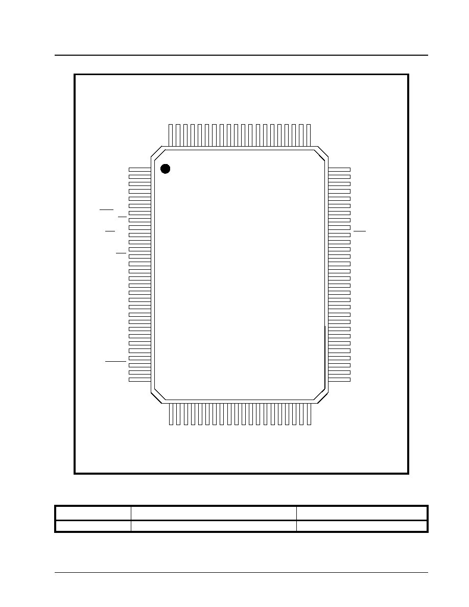
PINOUT OF XRT7250 - 100-LEAD PQFP PACKAGE
1
2
3
4
5
6
7
8
9
1 0
1 1
1 2
1 3
1 4
1 5
1 6
1 7
1 8
1 9
2 0
2 1
2 2
2 3
2 4
2 5
2 6
2 7
2 8
2 9
3 0
31
50
100
81
8 0
5 1
1 0 0 L e a d P Q F P
N C
N C
V D D
N C
G N D
R d y _ D t c k
W R _ R W
C S
A L E _ A S
R D _ D S
N C
N C
I N T
G N D
A 0
A 1
A 2
A 3
A 4
A 5
A 6
A 7
A 8
V D D
NibbleIntf
G N D
M O T O
R E S E T
G N D
V D D
GND
DQ
D1
D2
D3
D4
D5
D6
D7
VDD
TxFramRef
GND
TxInClk
TxAISEn
TxSer
TxNib0
TxNib1
TxNib2
TxNib3
GND
V D D
D M O
E x t L O S
R L O L
R x P O S
R x N E G
R x L i n e C l k
N C
G N D
R E Q
R L O O P
L L O O P
T A O S
T x L E V
E N C O D I S
T x P O S
T x N E G
TxLineClk
V D D
T x F r a m e
G N D
T x N i b C l k
T x N i b F r a m e
T x O H F r a m e
T x O H E n a b l e
T x O H I n d
T x O H
T x O H I n s
T x O H C l k
V D D
GND
RxNib3
RxNib2
RxNib1
RxNib0
RxSer
RxAIS
RxClk
GND
RxFrame
VDD
RxOutClk
RxRED
RxOOF
RxLOS
RxOHClk
RxOHInd
RxO
RxOHEnable
RxOHFrame
ORDERING INFORMATION
P
ART
N
UMBER
P
ACKAGE
O
PERATING
T
EMPERATURE
XRT7250IQ
100 pin PQFP (24x18x3 mm)
-40∞C to +85∞C

XRT7250
DS3/E3 FRAMER IC
·Á
·Á
·Á
·Á
REV. 1.1.1
I
TABLE OF CONTENTS
FEATURES ................................................................................................................................................ 1
APPLICATIONS ......................................................................................................................................... 1
BLOCK DIAGRAM OF XRT7250 ............................................................................................................... 1
ORDERING INFORMATION ......................................................................................... 2
TABLE OF CONTENTS ................................................................................................. I
LIST OF FIGURES ........................................................................................................ X
LIST OF TABLES ...................................................................................................... XVII
PIN DESCRIPTIONS .......................................................................................................... 3
ELECTRICAL CHARACTERISTICS ................................................................................ 18
ABSOLUTE MAXIMUMS .......................................................................................................................... 18
DC ELECTRICAL CHARACTERISTICS .................................................................................................. 18
AC ELECTRICAL CHARACTERISTICS .................................................................................................. 18
AC ELECTRICAL CHARACTERISTICS (CONT.) .................................................................................... 20
1.0 TIMING DIAGRAMS ......................................................................................................................... 25
2.0 THE MICROPROCESSOR INTERFACE BLOCK ............................................................................ 36
2.1 T
HE
M
ICROPROCESSOR
I
NTERFACE
B
LOCK
S
IGNAL
.......................................................................... 36
2.2 I
NTERFACING
THE
XRT7250 DS3/E3 F
RAMER
TO
THE
L
OCAL
µC/µP
VIA
THE
M
ICROPROCESSOR
I
NTER
-
FACE
B
LOCK
38
2.3 O
N
-C
HIP
R
EGISTER
O
RGANIZATION
.................................................................................................. 51
PART NUMBER REGISTER (ADDRESS = 0X02) ................................................................................... 58
VERSION NUMBER REGISTER (ADDRESS = 0X03) ............................................................................ 58
BLOCK INTERRUPT ENABLE REGISTER (ADDRESS = 0X04) ............................................................ 58
BLOCK INTERRUPT STATUS REGISTER (ADDRESS = 0X05) ............................................................ 59
RXDS3 CONFIGURATION & STATUS REGISTER (ADDRESS = 0X10) ............................................... 59
RXDS3 STATUS REGISTER (ADDRESS = 0X11) .................................................................................. 61
RXDS3 INTERRUPT ENABLE REGISTER (ADDRESS = 0X12) ............................................................ 61
RXDS3 INTERRUPT STATUS REGISTER (ADDRESS = 0X13) ............................................................ 62
RXDS3 SYNC DETECT ENABLE REGISTER (ADDRESS = 0X14) ....................................................... 63
RXDS3 FEAC INTERRUPT ENABLE/STATUS REGISTER (ADDRESS = 0X17) .................................. 64
RXDS3 LAPD CONTROL REGISTER (ADDRESS = 0X18) .................................................................... 65
RXDS3 LAPD STATUS REGISTER (ADDRESS = 0X19) ....................................................................... 65
RXE3 CONFIGURATION & STATUS REGISTER 1 (ADDRESS = 0X10) ............................................... 66
RXE3 CONFIGURATION & STATUS REGISTER 2 (ADDRESS = 0X11) ............................................... 67
RXE3 INTERRUPT ENABLE REGISTER - 1 (ADDRESS = 0X12) .......................................................... 68
RXE3 INTERRUPT ENABLE REGISTER - 2 (ADDRESS = 0X13) .......................................................... 69
RXE3 INTERRUPT STATUS REGISTER - 1 (ADDRESS = 0X14) .......................................................... 69
RXE3 INTERRUPT STATUS REGISTER - 2 (ADDRESS = 0X15) .......................................................... 70
RXE3 LAPD CONTROL REGISTER (ADDRESS = 0X18) ....................................................................... 71
RXE3 LAPD STATUS REGISTER (ADDRESS = 0X19) .......................................................................... 72
RXE3 NR BYTE REGISTER (ADDRESS = 0X1A) ................................................................................... 73
RXE3 GC BYTE REGISTER (ADDRESS = 0X1B) .................................................................................. 73
RXE3 TTB-0 REGISTER (ADDRESS = 0X1C) ........................................................................................ 73
RXE3 TTB-1 REGISTER (ADDRESS = 0X1D) ........................................................................................ 74
RXE3 TTB-2 REGISTER (ADDRESS = 0X1E) ........................................................................................ 74
RXE3 TTB-3 REGISTER (ADDRESS = 0X1F) ........................................................................................ 74
RXE3 TTB-4 REGISTER (ADDRESS = 0X20) ......................................................................................... 75
RXE3 TTB-5 REGISTER (ADDRESS = 0X21) ......................................................................................... 75

·Á
·Á
·Á
·Á
DS3/E3 FRAMER IC
XRT7250
REV. 1.1.1
II
RXE3 TTB-6 REGISTER (ADDRESS = 0X22) ........................................................................................ 75
RXE3 TTB-7 REGISTER (ADDRESS = 0X23) ........................................................................................ 75
RXE3 TTB-8 REGISTER (ADDRESS = 0X24) ........................................................................................ 76
RXE3 TTB-9 REGISTER (ADDRESS = 0X25) ........................................................................................ 76
RXE3 TTB-10 REGISTER (ADDRESS = 0X26) ...................................................................................... 76
RXE3 TTB-11 REGISTER (ADDRESS = 0X27) ...................................................................................... 77
RXE3 TTB-12 REGISTER (ADDRESS = 0X28) ...................................................................................... 77
RXE3 TTB-13 REGISTER (ADDRESS = 0X29 ....................................................................................... 77
RXE3 TTB-14 REGISTER (ADDRESS = 0X2A) ...................................................................................... 77
RXE3 TTB-15 REGISTER (ADDRESS = 0X2B) ...................................................................................... 78
RXE3 CONFIGURATION & STATUS REGISTER - 1 G.751 (ADDRESS = 0X10) ................................. 78
RXE3 CONFIGURATION & STATUS REGISTER - 2 (ADDRESS = 0X11) ............................................ 79
RXE3 INTERRUPT ENABLE REGISTER - 1 (ADDRESS = 0X12) ......................................................... 80
RXE3 INTERRUPT ENABLE REGISTER - 2 (ADDRESS = 0X13) ......................................................... 80
RXE3 INTERRUPT STATUS REGISTER - 1 (ADDRESS = 0X14) ......................................................... 81
RXE3 INTERRUPT STATUS REGISTER - 2 (ADDRESS = 0X15) ......................................................... 82
RXE3 LAPD CONTROL REGISTER (ADDRESS = 0X18) ...................................................................... 82
RXE3 LAPD STATUS REGISTER (ADDRESS = 0X19) ......................................................................... 83
RXE3 SERVICE BIT REGISTER (ADDRESS = 0X1A) ........................................................................... 84
TRANSMIT DS3 CONFIGURATION REGISTER (ADDRESS = 0X30) ................................................... 84
TRANSMIT DS3 FEAC CONFIGURATION & STATUS REGISTER (ADDRESS = 0X31) ...................... 85
TXDS3 FEAC REGISTER (ADDRESS = 0X32) ...................................................................................... 86
TXDS3 LAPD CONFIGURATION REGISTER (ADDRESS = 0X33) ....................................................... 86
TXDS3 LAPD STATUS AND INTERRUPT REGISTER (ADDRESS = 0X34) ......................................... 87
TXDS3 M-BIT MASK REGISTER (ADDRESS = 0X35) ........................................................................... 88
TXDS3 F-BIT MASK REGISTER - 1 (ADDRESS = 0X36) ...................................................................... 89
TXDS3 F-BIT MASK REGISTER - 2 (ADDRESS = 0X37) ...................................................................... 89
TXDS3 F-BIT MASK REGISTER - 3 (ADDRESS = 0X38) ...................................................................... 89
TXDS3 F-BIT MASK REGISTER - 4 (ADDRESS = 0X39) ...................................................................... 90
TXE3 CONFIGURATION REGISTER (ADDRESS = 0X30) .................................................................... 90
TXE3 LAPD CONFIGURATION REGISTER (ADDRESS = 0X33) .......................................................... 91
TXE3 LAPD STATUS AND INTERRUPT REGISTER (ADDRESS = 0X34) ............................................ 92
TXE3 GC BYTE REGISTER (ADDRESS = 0X35) ................................................................................... 92
TXE3 MA BYTE REGISTER (ADDRESS = 0X36) ................................................................................... 93
TXE3 NR BYTE REGISTER (ADDRESS = 0X37) ................................................................................... 93
TXE3 TTB-0 REGISTER (ADDRESS = 0X38) ........................................................................................ 93
TXE3 TTB-1 REGISTER (ADDRESS = 0X39) ........................................................................................ 94
TXE3 TTB-2 REGISTER (ADDRESS = 0X3A) ........................................................................................ 94
TXE3 TTB-3 REGISTER (ADDRESS = 0X3B) ........................................................................................ 94
TXE3 TTB-4 REGISTER (ADDRESS = 0X3C) ........................................................................................ 95
TXE3 TTB-5 REGISTER (ADDRESS = 0X3D) ........................................................................................ 95
TXE3 TTB-6 REGISTER (ADDRESS = 0X3E) ........................................................................................ 95
TXE3 TTB-7 REGISTER (ADDRESS = 0X3F) ........................................................................................ 96
TXE3 TTB-8 REGISTER (ADDRESS = 0X40) ........................................................................................ 96
TXE3 TTB-9 REGISTER (ADDRESS = 0X41) ........................................................................................ 96
TXE3 TTB-10 REGISTER (ADDRESS = 0X42) ...................................................................................... 97
TXE3 TTB-11 REGISTER (ADDRESS = 0X43) ...................................................................................... 97
TXE3 TTB-12 REGISTER (ADDRESS = 0X44) ...................................................................................... 98
TXE3 TTB-13 REGISTER (ADDRESS = 0X45) ...................................................................................... 98
TXE3 TTB-14 REGISTER (ADDRESS = 0X46) ...................................................................................... 98
TXE3 TTB-15 REGISTER (ADDRESS = 0X47) ...................................................................................... 99
TXE3 FA1 ERROR MASK REGISTER (ADDRESS = 0X48) ................................................................... 99
TXE3 FA2 ERROR MASK REGISTER (ADDRESS = 0X49) ................................................................... 99
TXE3 BIP-8 ERROR MASK REGISTER (ADDRESS = 0X4A) .............................................................. 100

XRT7250
DS3/E3 FRAMER IC
·Á
·Á
·Á
·Á
REV. 1.1.1
III
TXE3 CONFIGURATION REGISTER (ADDRESS = 0X30) ................................................................... 100
TXE3 LAPD CONFIGURATION REGISTER (ADDRESS = 0X33) ........................................................ 102
TXE3 LAPD STATUS AND INTERRUPT REGISTER (ADDRESS = 0X34) .......................................... 102
TXE3 SERVICE BITS REGISTER (ADDRESS = 0X35) ........................................................................ 103
TXE3 FAS ERROR MASK REGISTER - 0 (ADDRESS = 0X48) ............................................................ 103
TXE3 FAS ERROR MASK REGISTER - 1 (ADDRESS = 0X49) ............................................................ 104
TXE3 BIP-4 ERROR MASK REGISTER (ADDRESS = 0X4A) .............................................................. 104
PMON LCV EVENT COUNT REGISTER - LSB (ADDRESS = 0X51) ................................................... 105
PMON FRAMING BIT/BYTE ERROR COUNT REGISTER - MSB (ADDRESS = 0X52) ....................... 105
PMON FRAMING BIT/BYTE ERROR COUNT REGISTER - LSB (ADDRESS = 0X53) ........................ 105
PMON PARITY ERROR COUNT REGISTER - MSB (ADDRESS = 0X54) ........................................... 105
PMON PARITY ERROR COUNT REGISTER - LSB (ADDRESS = 0X55) ............................................ 106
PMON FEBE EVENT COUNT REGISTER - MSB (ADDRESS = 0X56) ................................................ 106
PMON FEBE EVENT COUNT REGISTER - LSB (ADDRESS = 0X57) ................................................. 106
PMON CP-BIT ERROR COUNT REGISTER - MSB (ADDRESS = 0X58) ............................................. 107
PMON CP-BIT ERROR COUNT REGISTER - LSB (ADDRESS = 0X59) .............................................. 107
PMON HOLDING REGISTER (ADDRESS = 0X6C) .............................................................................. 107
ONE-SECOND ERROR STATUS REGISTER (ADDRESS = 0X6D) ..................................................... 108
LCV - ONE-SECOND ACCUMULATOR REGISTER - MSB (ADDRESS = 0X6E) ................................ 108
LCV - ONE-SECOND ACCUMULATOR REGISTER - LSB (ADDRESS = 0X6F) ................................. 108
FRAME PARITY ERRORS - ONE-SECOND ACCUMULATOR REGISTER - MSB (ADDRESS = 0X70) ....
109
FRAME PARITY ERRORS - ONE-SECOND ACCUMULATOR REGISTER - LSB (ADDRESS = 0X71) .....
109
FRAME CP-BIT ERRORS - ONE-SECOND ACCUMULATOR REGISTER - MSB (ADDRESS = 0X72) .....
109
FRAME PARITY ERRORS - ONE-SECOND ACCUMULATOR REGISTER - LSB (ADDRESS = 0X73) .....
109
LINE INTERFACE DRIVE REGISTER (ADDRESS = 0X80) .................................................................. 110
LINE INTERFACE SCAN REGISTER (ADDRESS = 0X81) ................................................................... 112
2.4 T
HE
L
OSS
OF
C
LOCK
E
NABLE
F
EATURE
......................................................................................... 112
ADDRESS = 0X01, FRAMER I/O CONTROL REGISTER ..................................................................... 113
2.5 U
SING
THE
PMON H
OLDING
R
EGISTER
.......................................................................................... 113
2.6 T
HE
I
NTERRUPT
S
TRUCTURE
WITHIN
THE
F
RAMER
M
ICROPROCESSOR
I
NTERFACE
S
ECTION
............. 113
BLOCK INTERRUPT STATUS REGISTER (ADDRESS = 0X05) .......................................................... 115
BLOCK INTERRUPT ENABLE REGISTER (ADDRESS = 0X04) .......................................................... 116
FRAMER OPERATING MODE REGISTER (ADDRESS = 0X00) .......................................................... 118
2.7 I
NTERFACING
THE
FRAMER
TO
AN
INTEL
-
TYPE
MICROPROCESSOR
.................................................... 118
2.8 I
NTERFACING
THE
F
RAMER
IC
TO
A
M
OTOROLA
-
TYPE
M
ICROPROCESSOR
........................................ 121
3.0 THE LINE INTERFACE AND SCAN SECTION .............................................................................. 122
3.1 B
IT
-F
IELDS
WITHIN
THE
L
INE
I
NTERFACE
D
RIVE
R
EGISTER
.............................................................. 123
LINE INTERFACE DRIVE REGISTER (ADDRESS = 0X80) .................................................................. 123
3.2 B
IT
-F
IELDS
WITHIN
THE
L
INE
I
NTERFACE
S
CAN
R
EGISTER
............................................................... 125
LINE INTERFACE SCAN REGISTER (ADDRESS = 0X81) ................................................................... 126
XRT7250 CONFIGURATION .......................................................................................... 127
4.0 DS3 OPERATION OF THE XRT7250 ............................................................................................. 127
FRAMER OPERATING MODE REGISTER (ADDRESS = 0X00) .......................................................... 127
4.1 D
ESCRIPTION
OF
THE
DS3 F
RAMES
AND
A
SSOCIATED
O
VERHEAD
B
ITS
.......................................... 127
FRAMER OPERATING MODE REGISTER (ADDRESS = 0X00) .......................................................... 128
4.2 T
HE
T
RANSMIT
S
ECTION
OF
THE
XRT7250 (DS3 M
ODE
O
PERATION
) ............................................. 131

·Á
·Á
·Á
·Á
DS3/E3 FRAMER IC
XRT7250
REV. 1.1.1
IV
FRAMER OPERATING MODE REGISTER (ADDRESS = 0X00) ......................................................... 137
FRAMER OPERATING MODE REGISTER (ADDRESS = 0X00) ......................................................... 139
FRAMER OPERATING MODE REGISTER (ADDRESS = 0X00) ......................................................... 141
FRAMER OPERATING MODE REGISTER (ADDRESS = 0X00) ......................................................... 143
FRAMER OPERATING MODE REGISTER (ADDRESS = 0X00) ......................................................... 146
FRAMER OPERATING MODE REGISTER (ADDRESS = 0X00) ......................................................... 148
TX DS3 FEAC REGISTER (ADDRESS = 0X32) ................................................................................... 161
TRANSMIT DS3 FEAC CONFIGURATION AND STATUS REGISTER (ADDRESS = 0X31) ............... 161
TRANSMIT DS3 FEAC CONFIGURATION AND STATUS REGISTER (ADDRESS = 0X31) ............... 161
TRANSMIT DS3 LAPD CONFIGURATION REGISTER (ADDRESS = 0X33) ...................................... 164
TRANSMIT DS3 LAPD CONFIGURATION REGISTER (ADDRESS = 0X33) ...................................... 164
TRANSMIT DS3 LAPD STATUS/INTERRUPT REGISTER (ADDRESS = 0X34) ................................. 165
FRAMER OPERATING MODE REGISTER (ADDRESS = 0X00) ......................................................... 167
BLOCK INTERRUPT ENABLE REGISTER (ADDRESS = 0X04) ......................................................... 167
TX DS3 CONFIGURATION REGISTER (ADDRESS = 0X30) ............................................................... 169
TX DS3 M-BIT MASK REGISTER, ADDRESS = 0X35 ......................................................................... 172
TX DS3 F-BIT MASK1 REGISTER, ADDRESS = 0X36 ........................................................................ 172
TX DS3 F-BIT MASK2 REGISTER, ADDRESS = 0X37 ........................................................................ 173
TX DS3 F-BIT MASK3 REGISTER, ADDRESS = 0X38 ........................................................................ 173
TX DS3 F-BIT MASK4 REGISTER, ADDRESS = 0X39 ........................................................................ 173
I/O CONTROL REGISTER (ADDRESS = 0X01) ................................................................................... 176
I/O CONTROL REGISTER (ADDRESS = 0X01) ................................................................................... 178
II/O CONTROL REGISTER (ADDRESS = 0X01) .................................................................................. 178
BLOCK INTERRUPT ENABLE REGISTER (ADDRESS = 0X04) ......................................................... 180
TRANSMIT DS3 FEAC CONFIGURATION & STATUS REGISTER (ADDRESS = 0X31) .................... 180
TRANSMIT DS3 FEAC CONFIGURATION & STATUS REGISTER (ADDRESS = 0X31) .................... 181
TXDS3 LAPD STATUS AND INTERRUPT REGISTER (ADDRESS = 0X34) ....................................... 181
TXDS3 LAPD STATUS AND INTERRUPT REGISTER (ADDRESS = 0X34) ....................................... 182
4.3 T
HE
R
ECEIVE
S
ECTION
OF
THE
XRT7250 (DS3 M
ODE
O
PERATION
) ............................................... 182
II/O CONTROL REGISTER (ADDRESS = 0X01) .................................................................................. 184
II/O CONTROL REGISTER (ADDRESS = 0X01) .................................................................................. 187
RX DS3 CONFIGURATION AND STATUS REGISTER, (ADDRESS = 0X10) ..................................... 190
RX DS3 CONFIGURATION AND STATUS REGISTER, (ADDRESS = 0X10) ..................................... 191
RX DS3 CONFIGURATION AND STATUS REGISTER, (ADDRESS = 0X10) ..................................... 191
RX DS3 CONFIGURATION AND STATUS REGISTER, (ADDRESS = 0X10) ..................................... 192
I/O CONTROL REGISTER (ADDRESS = 0X01) ................................................................................... 192
PMON FRAMING BIT ERROR EVENT COUNT REGISTER - MSB (ADDRESS = 0X52) .................... 192
PMON FRAMING BIT ERROR EVENT COUNT REGISTER - LSB (ADDRESS = 0X53) ..................... 192
RX DS3 CONFIGURATION AND STATUS REGISTER, (ADDRESS = 0X10) ..................................... 193
RX DS3 CONFIGURATION AND STATUS REGISTER, (ADDRESS = 0X10) ..................................... 193
RX DS3 CONFIGURATION AND STATUS REGISTER, (ADDRESS = 0X10) ..................................... 194
RX DS3 CONFIGURATION AND STATUS REGISTER, (ADDRESS = 0X10) ..................................... 194
RX DS3 CONFIGURATION AND STATUS REGISTER, (ADDRESS = 0X10) ..................................... 194
RX DS3 STATUS REGISTER (ADDRESS = 0X11) .............................................................................. 195
RX DS3 INTERRUPT STATUS REGISTER (ADDRESS = 0X13) ......................................................... 195
RXDS3 STATUS REGISTER (ADDRESS = 0X11) ............................................................................... 196
RXDS3 INTERRUPT STATUS REGISTER (ADDRESS = 0X13) .......................................................... 196
PMON PARITY ERROR EVENT COUNT REGISTER - MSB (ADDRESS = 0X54) .............................. 196
PMON PARITY ERROR EVENT COUNT REGISTER - LSB (ADDRESS = 0X55) ............................... 197
RX DS3 FEAC INTERRUPT ENABLE/STATUS REGISTER (ADDRESS = 0X17) ............................... 200
RX DS3 FEAC REGISTER (ADDRESS = 0X16) ................................................................................... 200
RX DS3 FEAC INTERRUPT ENABLE/STATUS REGISTER (ADDRESS = 0X17) ............................... 200
RX DS3 LAPD CONTROL REGISTER (ADDRESS = 0X18) ................................................................ 202

XRT7250
DS3/E3 FRAMER IC
·Á
·Á
·Á
·Á
REV. 1.1.1
V
RX DS3 LAPD STATUS REGISTER (ADDRESS = 0X19) .................................................................... 202
BLOCK INTERRUPT ENABLE REGISTER (ADDRESS = 0X04) .......................................................... 222
RXDS3 INTERRUPT ENABLE REGISTER (ADDRESS = 0X12) .......................................................... 222
RXDS3 INTERRUPT STATUS REGISTER (ADDRESS = 0X13) .......................................................... 223
RXDS3 CONFIGURATION & STATUS REGISTER (ADDRESS = 0X10) ............................................. 223
RXDS3 INTERRUPT ENABLE REGISTER (ADDRESS = 0X12) .......................................................... 224
RXDS3 INTERRUPT STATUS REGISTER (ADDRESS = 0X13) .......................................................... 224
RXDS3 CONFIGURATION & STATUS REGISTER (ADDRESS = 0X10) ............................................. 224
RXDS3 INTERRUPT ENABLE REGISTER (ADDRESS = 0X12) .......................................................... 225
RXDS3 INTERRUPT STATUS REGISTER (ADDRESS = 0X13) .......................................................... 225
RXDS3 CONFIGURATION & STATUS REGISTER (ADDRESS = 0X10) ............................................. 226
RXDS3 INTERRUPT ENABLE REGISTER (ADDRESS = 0X12) .......................................................... 226
RXDS3 INTERRUPT STATUS REGISTER (ADDRESS = 0X13) .......................................................... 227
RXDS3 CONFIGURATION & STATUS REGISTER (ADDRESS = 0X10) ............................................. 227
RXDS3 INTERRUPT ENABLE REGISTER (ADDRESS = 0X12) .......................................................... 227
RXDS3 INTERRUPT STATUS REGISTER (ADDRESS = 0X13) .......................................................... 228
RXDS3 STATUS REGISTER (ADDRESS = 0X11) ................................................................................ 228
RXDS3 INTERRUPT ENABLE REGISTER (ADDRESS = 0X12) .......................................................... 228
RXDS3 INTERRUPT STATUS REGISTER (ADDRESS = 0X13) .......................................................... 229
RXDS3 INTERRUPT ENABLE REGISTER (ADDRESS = 0X12) .......................................................... 229
RXDS3 INTERRUPT STATUS REGISTER (ADDRESS = 0X13) .......................................................... 229
RXDS3 INTERRUPT ENABLE REGISTER (ADDRESS = 0X12) .......................................................... 230
RXDS3 INTERRUPT STATUS REGISTER (ADDRESS = 0X13) .......................................................... 230
RXDS3 FEAC INTERRUPT ENABLE/STATUS REGISTER (ADDRESS = 0X17) ................................ 231
RXDS3 FEAC INTERRUPT ENABLE/STATUS REGISTER (ADDRESS = 0X17) ................................ 231
RXDS3 FEAC INTERRUPT ENABLE/STATUS REGISTER (ADDRESS = 0X17) ................................ 232
RXDS3 FEAC INTERRUPT ENABLE/STATUS REGISTER (ADDRESS = 0X17) ................................ 232
RXDS3 LAPD CONTROL REGISTER (ADDRESS = 0X18) .................................................................. 233
RXDS3 LAPD CONTROL REGISTER (ADDRESS = 0X18) .................................................................. 233
5.0 E3/ITU-T G.751 OPERATION OF THE XRT7250 .......................................................................... 234
FRAMER OPERATING MODE REGISTER (ADDRESS = 0X00) .......................................................... 234
5.1 D
ESCRIPTION
OF
THE
E3, ITU-T G.751 F
RAMES
AND
A
SSOCIATED
O
VERHEAD
B
ITS
....................... 234
5.2 T
HE
T
RANSMIT
S
ECTION
OF
THE
XRT7250 (E3, ITU-T G.751 M
ODE
O
PERATION
) .......................... 235
TXE3 CONFIGURATION REGISTER (ADDRESS = 0X30) ................................................................... 239
FRAMER OPERATING MODE REGISTER (ADDRESS = 0X00) .......................................................... 241
FRAMER OPERATING MODE REGISTER (ADDRESS = 0X00) .......................................................... 243
FRAMER OPERATING MODE REGISTER (ADDRESS = 0X00) .......................................................... 245
FRAMER OPERATING MODE REGISTER (ADDRESS = 0X00) .......................................................... 247
FRAMER OPERATING MODE REGISTER (ADDRESS = 0X00) .......................................................... 250
FRAMER OPERATING MODE REGISTER (ADDRESS = 0X00) .......................................................... 252
TXE3 CONFIGURATION REGISTER (ADDRESS = 0X30) ................................................................... 264
TRANSMIT E3 LAPD CONFIGURATION REGISTER (ADDRESS = 0X33) .......................................... 264
TXE3 LAPD CONFIGURATION REGISTER (ADDRESS = 0X33) ........................................................ 265
TRANSMIT E3 LAPD CONFIGURATION REGISTER (ADDRESS = 0X33) .......................................... 265
TXE3 LAPD STATUS AND INTERRUPT REGISTER (ADDRESS = 0X34) .......................................... 266
TXE3 LAPD STATUS AND INTERRUPT REGISTER (ADDRESS = 0X34) .......................................... 266
BLOCK INTERRUPT ENABLE REGISTER (ADDRESS = 0X04) .......................................................... 269
TXE3 CONFIGURATION REGISTER (ADDRESS = 0X30) ................................................................... 271
TXE3 CONFIGURATION REGISTER (ADDRESS = 0X30) ................................................................... 272
TXE3 SERVICE BITS REGISTER (ADDRESS = 0X35) ........................................................................ 273
TXE3 CONFIGURATION REGISTER (ADDRESS = 0X30) ................................................................... 273
TXE3 CONFIGURATION REGISTER (ADDRESS = 0X30) ................................................................... 274
TXE3 FAS ERROR MASK REGISTER - 0 (ADDRESS = 0X48) ............................................................ 274

·Á
·Á
·Á
·Á
DS3/E3 FRAMER IC
XRT7250
REV. 1.1.1
VI
TXE3 FAS ERROR MASK REGISTER - 1 (ADDRESS = 0X49) ........................................................... 274
TXE3 BIP-4 ERROR MASK REGISTER (ADDRESS = 0X4A) .............................................................. 275
I/O CONTROL REGISTER (ADDRESS = 0X01) ................................................................................... 278
I/O CONTROL REGISTER (ADDRESS = 0X01) ................................................................................... 280
II/O CONTROL REGISTER (ADDRESS = 0X01) .................................................................................. 280
BLOCK INTERRUPT ENABLE REGISTER (ADDRESS = 0X04) ......................................................... 282
TXE3 LAPD STATUS AND INTERRUPT REGISTER (ADDRESS = 0X34) .......................................... 282
TXE3 LAPD STATUS AND INTERRUPT REGISTER (ADDRESS = 0X34) .......................................... 283
5.3 T
HE
R
ECEIVE
S
ECTION
OF
THE
XRT7250 (E3 M
ODE
O
PERATION
) .................................................. 283
II/O CONTROL REGISTER (ADDRESS = 0X01) .................................................................................. 285
II/O CONTROL REGISTER (ADDRESS = 0X01) .................................................................................. 288
RXE3 INTERRUPT STATUS REGISTER - 1 (ADDRESS = 0X14) ....................................................... 292
RXE3 CONFIGURATION & STATUS REGISTER - 2 (ADDRESS = 0X11) .......................................... 293
RXE3 INTERRUPT STATUS REGISTER - 1 (ADDRESS = 0X14) ....................................................... 293
RXE3 INTERRUPT STATUS REGISTER - 1 (ADDRESS = 0X14) ....................................................... 293
RXE3 CONFIGURATION & STATUS REGISTER - 2 (ADDRESS = 0X11) .......................................... 294
PMON FRAMING BIT/BYTE ERROR COUNT REGISTER - MSB (ADDRESS = 0X52) ...................... 294
PMON FRAMING BIT/BYTE ERROR COUNT REGISTER - LSB (ADDRESS = 0X53) ....................... 294
RXE3 CONFIGURATION & STATUS REGISTER - 2 (ADDRESS = 0X11) .......................................... 295
RXE3 CONFIGURATION & STATUS REGISTER - 2 (ADDRESS = 0X11) .......................................... 296
RXE3 INTERRUPT STATUS REGISTER - 1 (ADDRESS = 0X14) ....................................................... 296
RXE3 CONFIGURATION & STATUS REGISTER - 2 (ADDRESS = 0X11) .......................................... 296
RXE3 INTERRUPT STATUS REGISTER - 1 (ADDRESS = 0X14) ....................................................... 297
RXE3 CONFIGURATION & STATUS REGISTER - 2 (ADDRESS = 0X11) .......................................... 297
RXE3 CONFIGURATION & STATUS REGISTER - 2 (ADDRESS = 0X11) .......................................... 297
RXE3 CONFIGURATION & STATUS REGISTER - 1 G.751 (ADDRESS = 0X10) ............................... 298
RXE3 INTERRUPT STATUS REGISTER - 2 (ADDRESS = 0X15) ....................................................... 298
RXE3 CONFIGURATION & STATUS REGISTER - 2 (ADDRESS = 0X11) .......................................... 298
RXE3 CONFIGURATION & STATUS REGISTER - 2 (ADDRESS = 0X11) .......................................... 299
RXE3 INTERRUPT STATUS REGISTER - 2 (ADDRESS = 0X15) ....................................................... 302
PMON PARITY ERROR COUNT REGISTER - MSB (ADDRESS = 0X54) ........................................... 302
PMON PARITY ERROR COUNT REGISTER - LSB (ADDRESS = 0X55) ............................................ 302
TXE3 CONFIGURATION REGISTER (ADDRESS = 0X30) .................................................................. 302
RXE3 INTERRUPT ENABLE REGISTER - 2 (ADDRESS = 0X13) ....................................................... 303
RXE3 LAPD CONTROL REGISTER (ADDRESS = 0X18 ..................................................................... 304
RXE3 LAPD STATUS REGISTER (ADDRESS = 0X19) ....................................................................... 305
RXE3 LAPD STATUS REGISTER (ADDRESS = 0X19) ....................................................................... 305
RXE3 LAPD STATUS REGISTER (ADDRESS = 0X19) ....................................................................... 306
RXE3 LAPD STATUS REGISTER (ADDRESS = 0X19) ....................................................................... 306
RXE3 LAPD STATUS REGISTER (ADDRESS = 0X19) ....................................................................... 306
RXE3 LAPD CONTROL REGISTER (ADDRESS = 0X18 ..................................................................... 307
RXE3 LAPD STATUS REGISTER (ADDRESS = 0X19) ....................................................................... 307
BLOCK INTERRUPT ENABLE REGISTER (ADDRESS = 0X04) ......................................................... 322
RXE3 INTERRUPT ENABLE REGISTER - 1 (ADDRESS = 0X12) ....................................................... 322
RXE3 INTERRUPT STATUS REGISTER - 1 (ADDRESS = 0X14) ....................................................... 323
RXE3 CONFIGURATION & STATUS REGISTER - 2 (ADDRESS = 0X11) .......................................... 323
RXE3 INTERRUPT ENABLE REGISTER - 1 (ADDRESS = 0X12) ....................................................... 324
RXE3 INTERRUPT STATUS REGISTER - 1 (ADDRESS = 0X14) ....................................................... 324
RXE3 CONFIGURATION & STATUS REGISTER 2 (ADDRESS = 0X11) ............................................ 324
RXE3 INTERRUPT ENABLE REGISTER - 1 (ADDRESS = 0X12) ....................................................... 325
RXE3 CONFIGURATION & STATUS REGISTER - 2 (ADDRESS = 0X11) .......................................... 325
RXE3 INTERRUPT ENABLE REGISTER - 1 (ADDRESS = 0X12) ....................................................... 326
RXE3 CONFIGURATION & STATUS REGISTER - 2 (ADDRESS = 0X11) .......................................... 326

XRT7250
DS3/E3 FRAMER IC
·Á
·Á
·Á
·Á
REV. 1.1.1
VII
RXE3 INTERRUPT ENABLE REGISTER - 1 (ADDRESS = 0X12) ........................................................ 327
RXE3 INTERRUPT STATUS REGISTER - 1 (ADDRESS = 0X14) ........................................................ 327
RXE3 INTERRUPT ENABLE REGISTER - 2 (ADDRESS = 0X13) ........................................................ 328
RXE3 INTERRUPT STATUS REGISTER - 2 (ADDRESS = 0X15) ........................................................ 328
RXE3 CONFIGURATION & STATUS REGISTER - 2 (ADDRESS = 0X11) ........................................... 328
RXE3 INTERRUPT ENABLE REGISTER - 2 (ADDRESS = 0X13) ........................................................ 329
RXE3 INTERRUPT STATUS REGISTER - 2 (ADDRESS = 0X15) ........................................................ 329
RXE3 INTERRUPT ENABLE REGISTER - 2 (ADDRESS = 0X13) ........................................................ 330
RXE3 INTERRUPT STATUS REGISTER - 2 (ADDRESS = 0X15) ........................................................ 330
RXE3 LAPD CONTROL REGISTER (ADDRESS = 0X18) ..................................................................... 330
RXE3 LAPD CONTROL REGISTER (ADDRESS = 0X18) ..................................................................... 331
6.0 E3/ITU-T G.832 OPERATION OF THE XRT7250 .......................................................................... 332
FRAMER OPERATING MODE REGISTER (ADDRESS = 0X00) .......................................................... 332
6.1 D
ESCRIPTION
OF
THE
E3, ITU-T G.832 F
RAMES
AND
A
SSOCIATED
O
VERHEAD
B
YTES
.................... 332
FRAMER OPERATING MODE REGISTER (ADDRESS = 0X00) .......................................................... 333
THE MAINTENANCE AND ADAPTATION (MA) BYTE FORMAT ......................................................... 334
6.2 T
HE
T
RANSMIT
S
ECTION
OF
THE
XRT7250 (E3 M
ODE
O
PERATION
) ................................................ 335
FRAMER OPERATING MODE REGISTER (ADDRESS = 0X00) .......................................................... 341
FRAMER OPERATING MODE REGISTER (ADDRESS = 0X00) .......................................................... 343
FRAMER OPERATING MODE REGISTER (ADDRESS = 0X00) .......................................................... 345
FRAMER OPERATING MODE REGISTER (ADDRESS = 0X00) .......................................................... 347
FRAMER OPERATING MODE REGISTER (ADDRESS = 0X00) .......................................................... 350
FRAMER OPERATING MODE REGISTER (ADDRESS = 0X00) .......................................................... 352
TRANSMIT E3 LAPD CONFIGURATION REGISTER (ADDRESS = 0X33) .......................................... 367
TXE3 CONFIGURATION REGISTER (ADDRESS = 0X30) ................................................................... 368
TXE3 LAPD CONFIGURATION REGISTER (ADDRESS = 0X33) ........................................................ 368
TRANSMIT E3 LAPD CONFIGURATION REGISTER (ADDRESS = 0X33) .......................................... 368
TXE3 LAPD STATUS AND INTERRUPT REGISTER (ADDRESS = 0X34) .......................................... 369
TXE3 LAPD STATUS AND INTERRUPT REGISTER (ADDRESS = 0X34) .......................................... 370
BLOCK INTERRUPT ENABLE REGISTER (ADDRESS = 0X04) .......................................................... 373
TXE3 CONFIGURATION REGISTER (ADDRESS = 0X30) ................................................................... 375
I/O CONTROL REGISTER (ADDRESS = 0X01) .................................................................................... 379
I/O CONTROL REGISTER (ADDRESS = 0X01) .................................................................................... 381
II/O CONTROL REGISTER (ADDRESS = 0X01) ................................................................................... 381
BLOCK INTERRUPT ENABLE REGISTER (ADDRESS = 0X04) .......................................................... 383
TXE3 LAPD STATUS AND INTERRUPT REGISTER (ADDRESS = 0X34) .......................................... 383
TXE3 LAPD STATUS AND INTERRUPT REGISTER (ADDRESS = 0X34) .......................................... 384
6.3 T
HE
R
ECEIVE
S
ECTION
OF
THE
XRT7250 (E3 M
ODE
O
PERATION
) .................................................. 384
II/O CONTROL REGISTER (ADDRESS = 0X01) ................................................................................... 386
II/O CONTROL REGISTER (ADDRESS = 0X01) ................................................................................... 389
RXE3 INTERRUPT STATUS REGISTER - 1 (ADDRESS = 0X14) ........................................................ 394
RXE3 CONFIGURATION & STATUS REGISTER 2 (ADDRESS = 0X11) ............................................. 394
RXE3 INTERRUPT STATUS REGISTER - 1 (ADDRESS = 0X14) ........................................................ 395
RXE3 INTERRUPT STATUS REGISTER - 1 (ADDRESS = 0X14) ........................................................ 395
RXE3 CONFIGURATION & STATUS REGISTER 2 (ADDRESS = 0X11) ............................................. 395
PMON FRAMING BIT/BYTE ERROR COUNT REGISTER - MSB (ADDRESS = 0X52) ....................... 396
PMON FRAMING BIT/BYTE ERROR COUNT REGISTER - LSB (ADDRESS = 0X53) ........................ 396
RXE3 CONFIGURATION & STATUS REGISTER 2 (ADDRESS = 0X11) ............................................. 396
RXE3 CONFIGURATION & STATUS REGISTER 2 (ADDRESS = 0X11) ............................................. 397
RXE3 INTERRUPT STATUS REGISTER - 1 (ADDRESS = 0X14) ........................................................ 397
RXE3 CONFIGURATION & STATUS REGISTER 2 (ADDRESS = 0X11) ............................................. 398
RXE3 INTERRUPT STATUS REGISTER - 1 (ADDRESS = 0X14) ........................................................ 398

·Á
·Á
·Á
·Á
DS3/E3 FRAMER IC
XRT7250
REV. 1.1.1
VIII
RXE3 CONFIGURATION & STATUS REGISTER 2 (ADDRESS = 0X11) ............................................ 398
RXE3 CONFIGURATION & STATUS REGISTER 2 (ADDRESS = 0X11) ............................................ 399
THE MAINTENANCE AND ADAPTATION (MA) BYTE FORMAT ......................................................... 399
RXE3 CONFIGURATION & STATUS REGISTER 1 - (E3, ITU-T G.832) (ADDRESS = 0X10) ............ 399
RXE3 INTERRUPT ENABLE REGISTER - 2 (ADDRESS = 0X13) ....................................................... 400
RXE3 CONFIGURATION & STATUS REGISTER 2 (ADDRESS = 0X11) ............................................ 400
RXE3 CONFIGURATION & STATUS REGISTER 2 (ADDRESS = 0X11) ............................................ 400
RXE3 INTERRUPT STATUS REGISTER - 2 (ADDRESS = 0X15) ....................................................... 403
PMON PARITY ERROR COUNT REGISTER - MSB (ADDRESS = 0X54) ........................................... 403
PMON PARITY ERROR COUNT REGISTER - LSB (ADDRESS = 0X55) ............................................ 404
RXE3 INTERRUPT STATUS REGISTER - 2 (ADDRESS = 0X15) ....................................................... 404
PMON FEBE EVENT COUNT REGISTER - MSB (ADDRESS = 0X56) ............................................... 404
PMON FEBE EVENT COUNT REGISTER - LSB (ADDRESS = 0X57) ................................................ 404
RXE3 INTERRUPT STATUS REGISTER - 2 (ADDRESS = 0X15) ....................................................... 405
RXE3 LAPD CONTROL REGISTER (ADDRESS = 0X18) .................................................................... 407
RXE3 LAPD CONTROL REGISTER (ADDRESS = 0X18) .................................................................... 407
RXE3 LAPD STATUS REGISTER (ADDRESS = 0X19) ....................................................................... 407
RXE3 LAPD STATUS REGISTER (ADDRESS = 0X19) ....................................................................... 408
RXE3 LAPD STATUS REGISTER (ADDRESS = 0X19) ....................................................................... 408
RXE3 LAPD STATUS REGISTER (ADDRESS = 0X19) ....................................................................... 409
RXE3 LAPD STATUS REGISTER (ADDRESS = 0X19) ....................................................................... 409
RXE3 LAPD CONTROL REGISTER (ADDRESS = 0X18) .................................................................... 410
RXE3 LAPD STATUS REGISTER (ADDRESS = 0X19) ....................................................................... 410
BLOCK INTERRUPT ENABLE REGISTER (ADDRESS = 0X04) ......................................................... 429
RXE3 INTERRUPT ENABLE REGISTER - 1 (ADDRESS = 0X12) ....................................................... 429
RXE3 INTERRUPT STATUS REGISTER - 1 (ADDRESS = 0X14) ....................................................... 430
RXE3 CONFIGURATION & STATUS REGISTER 2 (ADDRESS = 0X11) ............................................ 430
RXE3 INTERRUPT ENABLE REGISTER - 1 (ADDRESS = 0X12) ....................................................... 431
RXE3 INTERRUPT STATUS REGISTER - 1 (ADDRESS = 0X14) ....................................................... 431
RXE3 CONFIGURATION & STATUS REGISTER 2 (ADDRESS = 0X11) ............................................ 431
RXE3 INTERRUPT ENABLE REGISTER - 1 (ADDRESS = 0X12) ....................................................... 432
RXE3 CONFIGURATION & STATUS REGISTER 2 (ADDRESS = 0X11) ............................................ 432
RXE3 INTERRUPT ENABLE REGISTER - 1 (ADDRESS = 0X12) ....................................................... 433
RXE3 INTERRUPT STATUS REGISTER - 1 (ADDRESS = 0X14) ....................................................... 433
RXE3 INTERRUPT ENABLE REGISTER - 1 (ADDRESS = 0X12) ....................................................... 433
RXE3 INTERRUPT STATUS REGISTER - 1 (ADDRESS = 0X14) ....................................................... 434
RXE3 CONFIGURATION & STATUS REGISTER 2 (ADDRESS = 0X11) ............................................ 434
RXE3 INTERRUPT ENABLE REGISTER - 2 (ADDRESS = 0X13) ....................................................... 434
RXE3 INTERRUPT STATUS REGISTER - 2 (ADDRESS = 0X15) ....................................................... 435
RXE3 INTERRUPT ENABLE REGISTER - 2 (ADDRESS = 0X13) ....................................................... 435
RXE3 INTERRUPT STATUS REGISTER - 2 (ADDRESS = 0X15) ....................................................... 436
RXE3 CONFIGURATION & STATUS REGISTER 2 (ADDRESS = 0X11) ............................................ 436
RXE3 INTERRUPT ENABLE REGISTER - 2 (ADDRESS = 0X13) ....................................................... 436
RXE3 INTERRUPT STATUS REGISTER - 2 (ADDRESS = 0X15) ....................................................... 437
RXE3 INTERRUPT ENABLE REGISTER - 2 (ADDRESS = 0X13) ....................................................... 437
RXE3 INTERRUPT STATUS REGISTER - 2 (ADDRESS = 0X15) ....................................................... 437
RXE3 INTERRUPT ENABLE REGISTER - 2 (ADDRESS = 0X13) ....................................................... 438
RXE3 INTERRUPT STATUS REGISTER - 2 (ADDRESS = 0X15) ....................................................... 438
RXE3 CONFIGURATION & STATUS REGISTER 1 (ADDRESS = 0X10) ............................................ 439
RXE3 INTERRUPT ENABLE REGISTER - 2 (ADDRESS = 0X13) ....................................................... 439
RXE3 INTERRUPT STATUS REGISTER - 2 (ADDRESS = 0X15) ....................................................... 439
RXE3 LAPD CONTROL REGISTER (ADDRESS = 0X18) .................................................................... 440
RXE3 LAPD CONTROL REGISTER (ADDRESS = 0X18) .................................................................... 440

XRT7250
DS3/E3 FRAMER IC
·Á
·Á
·Á
·Á
REV. 1.1.1
IX
7.0 DIAGNOSTIC OPERATION OF THE XRT7250 FRAMER IC ........................................................ 441
ORDERING INFORMATION ..................................................................................... 443
PACKAGE DIMENSIONS ......................................................................................... 443
REVISION HISTORY ............................................................................................................................. 444

·Á
·Á
·Á
·Á
DS3/E3 FRAMER IC
XRT7250
REV. 1.1.1
X
LIST OF FIGURES
Figure 1.Timing Diagram for Transmit Payload Input Interface, when the XRT7250 Device is operating in both
the DS3 and Loop-Timing Modes ................................................................................................................... 25
Figure 2.Timing Diagram for the Transmit Payload Input Interface, when the XRT7250 Device is operating in
both the DS3 and Local-Timing Modes .......................................................................................................... 25
Figure 3.Timing Diagram for the Transmit Payload Data Input Interface, when the XRT7250 Device is operating
in both the DS3/Nibble and Looped-Timing Modes ........................................................................................ 26
Figure 4.Timing Diagram for the Transmit Payload Data Input Interface, when the XRT7250 Device is operating
in the DS3/Nibble and Local-Timing Modes ................................................................................................... 26
Figure 5.Timing Diagram for the Transmit Overhead Data Input Interface (Method 1 Access) ..................... 27
Figure 6.Timing Diagram for the Transmit Overhead Data Input Interface (Method 2 Access) ..................... 27
Figure 7.Transmit LIU Interface Timing - Framer is configured to update "TxPOS" and "TxNEG" on the rising
edge of "TxLineClk" ........................................................................................................................................ 28
Figure 8.Transmit LIU Interface Timing - Framer is configured to update "TxPOS" and "TxNEG" on the falling
edge of "TxLineClk" ........................................................................................................................................ 28
Figure 9.Receive LIU Interface Timing - Framer is configured to sample "RxPOS" and "RxNEG" on the rising
edge of "RxLineClk" ........................................................................................................................................ 29
Figure 10.Receiver LIU Interface Timing - Framer is configured to sample "RxPOS" and "RxNEG" on the falling
edge of "RxLineClk" ........................................................................................................................................ 29
Figure 11.Receive Payload Data Output Interface Timing ............................................................................. 30
Figure 12.Receive Payload Data Output Interface Timing (Nibble Mode Operation) ..................................... 30
Figure 13.Receive Overhead Data Output Interface Timing (Method 1 - Using RxOHClk) ............................ 31
Figure 14.Receive Overhead Data Output Interface Timing (Method 2 - Using RxOHEnable) ...................... 31
Figure 15.Microprocessor Interface Timing - Intel Type Programmed I/O Read Operations ......................... 32
Figure 16.Microprocessor Interface Timing - Intel Type Programmed I/O Write Operations ......................... 32
Figure 17.Microprocessor Interface Timing - Intel Type Read Burst Access Operation ................................. 33
Figure 18.Microprocessor Interface Timing - Intel Type Write Burst Access Operation ................................. 33
Figure 19.Microprocessor Interface Timing - Motorola Type Programmed I/O Read Operation .................... 34
Figure 20.Microprocessor Interface Timing - Motorola Type Programmed I/O Write Operation .................... 34
Figure 21.Microprocessor Interface Timing - Motorola Type Read Burst Access Operation ......................... 35
Figure 22.Microprocessor Interface Timing - Motorola Type Write Burst Access Operation .......................... 35
Figure 23.Microprocessor Interface Timing - Reset Pulse Width ................................................................... 35
Figure 24.Simple Block Diagram of the Microprocessor Interface Block, within the Framer IC ..................... 36
Figure 25.Behavior of Microprocessor Interface signals during an Intel-type Programmed I/O Read Operation
40
Figure 26.Behavior of the Microprocessor Interface Signals, during an Intel-type Programmed I/O Write Opera-
tion .................................................................................................................................................................. 41
Figure 27.Illustration of the Behavior of Microprocessor Interface signals, during a Motorola-type Programmed
I/O Read Operation ........................................................................................................................................ 42
Figure 28.Illustration of the Behavior of the Microprocessor Interface signal, during a Motorola-type Pro-
grammed I/O Write Operation ........................................................................................................................ 43
Figure 29.Behavior of the Microprocessor Interface Signals, during the Initial Read Operation of a Burst Cycle
(Intel Type Processor) .................................................................................................................................... 44
Figure 30.Behavior of the Microprocessor Interface Signals, during subsequent Read Operations within the
Burst I/O Cycle ............................................................................................................................................... 45
Figure 31.Behavior of the Microprocessor Interface signals, during the Initial Write Operation of a Burst Cycle
(Intel-type Processor) ..................................................................................................................................... 46
Figure 32.Behavior of the Microprocessor Interface Signals, during subsequent Write Operations within the
Burst I/O Cycle ............................................................................................................................................... 47
Figure 33.Behavior of the Microprocessor Interface Signals, during the Initial Read Operation of a Burst Cycle
(Motorola Type Processor) ............................................................................................................................. 48
Figure 34.Behavior the Microprocessor Interface Signals, during subsequent Read Operations within the Burst
I/O Cycle (Motorola-type µC/µP) .................................................................................................................... 49

XRT7250
DS3/E3 FRAMER IC
·Á
·Á
·Á
·Á
REV. 1.1.1
XI
Figure 35.Behavior of the Microprocessor Interface signals, during the Initial Write Operation of a Burst Cycle
(Motorola-type Processor) .............................................................................................................................. 50
Figure 36.Behavior of the Microprocessor Interface Signals, during subsequent Write Operations with the Burst
I/O Cycle (Motorola-type µC/µP) ..................................................................................................................... 51
Figure 37.Schematic depicting how to interface the XRT7250 DS3/E3 Framer IC to the 8051 Microcontroller ..
120
Figure 38.Schematic Depicting how to interface the XRT7250 DS3/E3 Framer IC to the MC68000 Microproces-
sor ................................................................................................................................................................. 121
Figure 39.Schematic Depicting how to interface the XRT7250 DS3/E3 Framer IC to the XRT7300 DS3/E3/STS-
1 LIU IC ......................................................................................................................................................... 123
Figure 40.DS3 Frame Format for C-bit Parity ............................................................................................... 127
Figure 41.DS3 Frame Format for M13 .......................................................................................................... 128
Figure 42.A Simple Illustration of the Transmit Section, within the XRT7250, when it has been configured to op-
erate in the DS3 Mode .................................................................................................................................. 132
Figure 43.A Simple Illustration of the Transmit Payload Data Input Interface Block ..................................... 133
Figure 44.Illustration of the Terminal Equipment being interfaced to the Transmit Payload Data Input Interface
block (of the XRT7250) for Mode 1(Serial/Loop-Timing) Operation .............................................................. 136
Figure 45.Behavior of the Terminal Interface signals between the Transmit Payload Data Input Interface block
of the XRT7250 and the Terminal Equipment (for Mode 1 Operation) ......................................................... 137
Figure 46.Illustration of the Terminal Equipment being interfaced to the Transmit Payload Data Input Interface
block of the XRT7250 for Mode 2 (Serial/Local-Timed/Frame-Slave) Operation .......................................... 138
Figure 47.Behavior of the Terminal Interface signals between the XRT7250 and the Terminal Equipment (Mode
2 Operation) .................................................................................................................................................. 139
Figure 48.Illustration of the Terminal Equipment being interfaced to the Transmit Payload Data Input Interface
block of the XRT7250 for Mode 3 (Serial/Local-Timed/Frame-Master) Operation ........................................ 140
Figure 49.Behavior of the Terminal Interface signals between the XRT7250 and the Terminal Equipment (DS3
Mode 3 Operation) ........................................................................................................................................ 141
Figure 50.Illustration of the Terminal Equipment being interfaced to the Transmit Payload Data Input Interface
block of the XRT7250 for Mode 4 (Nibble-Parallel/Loop-Timed) Operation .................................................. 142
Figure 51.Behavior of the Terminal Interface signals between the XRT7250 and the Terminal Equipment (Mode
4 Operation) .................................................................................................................................................. 143
Figure 52.Illustration of the Terminal Equipment being interfaced to the Transmit Payload Data Input Interface
block of the XRT7250 for Mode 5 (Nibble-Parallel/Local-Timed/Frame-Slave) Operation ........................... 145
Figure 53.Behavior of the Terminal Interface signals between the XRT7250 and the Terminal Equipment (DS3
Mode 5 Operation) ........................................................................................................................................ 146
Figure 54.Illustration of the Terminal Equipment being interfaced to the Transmit Payload Data Input Interface
block of the XRT7250 for Mode 6 (Nibble-Parallel/Local-Timed/Frame-Master) Operation ......................... 147
Figure 55.Behavior of the Terminal Interface signals between the XRT7250 and the Terminal Equipment (DS3
Mode 6 Operation) ........................................................................................................................................ 148
Figure 56.Simple Illustration of the Transmit Overhead Data Input Interface block ...................................... 149
Figure 57.Illustration of the Terminal Equipment being interfaced to the Transmit Overhead Data Input Interface
(Method 1) ..................................................................................................................................................... 152
Figure 58.Illustration of the signal that must occur between the Terminal Equipment and the XRT7250, in order
to configure the XRT7250 to transmit a Yellow Alarm to the remote terminal equipment ............................. 155
Figure 59.Illustration of the Terminal Equipment being interfaced to the Transmit Overhead Data Input Interface
(Method 2) ..................................................................................................................................................... 157
Figure 60.Behavior of Transmit Overhead Data Input Interface signals between the XRT7250 and the Terminal
Equipment (for Method 2) ............................................................................................................................. 160
Figure 61.A Flow Chart depicting how to transmit a FEAC Message via the FEAC Transmitter .................. 162
Figure 62.LAPD Message Frame Format ..................................................................................................... 163
Figure 63.Flow Chart depict how to use the LAPD Transmitter .................................................................... 166
Figure 64.A Simple Illustration of the Transmit DS3 Framer Block and the associated paths to other Functional
Blocks ........................................................................................................................................................... 168
Figure 65.Approach to Interfacing the XRT7250 Framer IC to the XRT7300 DS3/E3/STS-1 Transmitter LIU ....

·Á
·Á
·Á
·Á
DS3/E3 FRAMER IC
XRT7250
REV. 1.1.1
XII
174
Figure 66.A Simple Illustration of the Transmit DS3 LIU Interface block ...................................................... 175
Figure 67.The Behavior of TxPOS and TxNEG signals during data transmission while the Transmit DS3 LIU In-
terface is operating in the Unipolar Mode ..................................................................................................... 175
Figure 68.Illustration of AMI Line Code ........................................................................................................ 177
Figure 69.Illustration of two examples of B3ZS Encoding ............................................................................ 177
Figure 70.Waveform/Timing Relationship between TxLineClk, TxPOS and TxNEG - TxPOS and TxNEG are
configured to be updated on the rising edge of TxLineClk ........................................................................... 179
Figure 71.Waveform/Timing Relationship between TxLineClk, TxPOS and TxNEG - TxPOS and TxNEG are
configured to be updated on the falling edge of TxLineClk .......................................................................... 179
Figure 72.A Simple Illustration of the Receive Section of the XRT7250, when it has been configured to operate
in the DS3 Mode ........................................................................................................................................... 182
Figure 73.A Simple Illustration of the Receive DS3 LIU Interface Block ...................................................... 183
Figure 74.Behavior of the RxPOS, RxNEG and RxLineClk signals during data reception of Unipolar Data 184
Figure 75.Illustration on how the Receive DS3 Framer (within the XRT7250 Framer IC) being interface to
theXRT7300 Line Interface Unit, while the Framer is operating in Bipolar Mode ......................................... 185
Figure 76.Illustration of AMI Line Code ........................................................................................................ 185
Figure 77.Illustration of two examples of B3ZS Decoding ............................................................................ 186
Figure 78.Waveform/Timing Relationship between RxLineClk, RxPOS and RxNEG - When RxPOS and RxNEG
are to be sampled on the rising edge of RxLineClk ...................................................................................... 187
Figure 79.Waveform/Timing Relationship between RxLineClk, RxPOS and RxNEG - When RxPOS and RxNEG
are to be sampled on the falling edge of RxLineClk ..................................................................................... 188
Figure 80.A Simple Illustration of the Receive DS3 Framer Block and the Associated Paths to the Other Func-
tional Blocks ................................................................................................................................................. 188
Figure 81.The State Machine Diagram for the Receive DS3 Framer block's Frame Acquisition/Maintenance Al-
gorithm .......................................................................................................................................................... 189
Figure 82.A Simple Illustration of the Locations of the Source, Mid-Network and Sink Terminal Equipment (for
CP-Bit Processing) ....................................................................................................................................... 197
Figure 83.Illustration of the Presumed Configuration of the Mid-Network Terminal Equipment ................... 198
Figure 84.Flow Diagram depicting how the Receive FEAC Processor Functions ........................................ 201
Figure 85.LAPD Message Frame Format ..................................................................................................... 202
Figure 86.Flow Chart depicting the Functionality of the LAPD Receiver ...................................................... 204
Figure 87.A Simple Illustration of the Receive Overhead Output Interface block ......................................... 205
Figure 88.Illustration of how to interface the Terminal Equipment to the Receive Overhead Data Output Interface
block (for Method 1). ..................................................................................................................................... 207
Figure 89.Illustration of the signals that are output via the Receive Overhead Output Interface (for Method 1).
210
Figure 90.Illustration of how to interface the Terminal Equipment to the Receive Overhead Data Output Interface
block (for Method 2). ..................................................................................................................................... 212
Figure 91.Illustration of the signals that are output via the Receive Overhead Data Output Interface block (for
Method 2). .................................................................................................................................................... 215
Figure 92.A Simple illustration of the Receive Payload Data Output Interface block ................................... 216
Figure 93.Illustration of the XRT7250 DS3/E3 Framer IC being interfaced to the Receive Terminal Equipment
(Serial Mode Operation) ............................................................................................................................... 218
Figure 94.An Illustration of the behavior of the signals between the Receive Payload Data Output Interface block
of the XRT7250 and the Terminal Equipment (Serial Mode Operation) ....................................................... 219
Figure 95.Illustration of the XRT7250 DS3/E3 Framer IC being interfaced to the Receive Section of the Terminal
Equipment (Nibble-Mode Operation) ............................................................................................................ 220
Figure 96.An Illustration of the Behavior of the signals between the Receive Payload Data Output Interface
Block of the XRT7250 and the Terminal Equipment (Nibble-Mode Operation). ........................................... 221
Figure 97.Illustration of the E3, ITU-T G.751 Framing Format. .................................................................... 234
Figure 98.A Simple Illustration of the XRT7250 Transmit Section when it has been configured to operate in the
E3 Mode ....................................................................................................................................................... 235
Figure 99.A Simple Illustration of the Transmit Payload Data Input Interface Block .................................... 236

XRT7250
DS3/E3 FRAMER IC
·Á
·Á
·Á
·Á
REV. 1.1.1
XIII
Figure 100.Illustration of the Terminal Equipment being interfaced to the Transmit Payload Data Input Interface
block of the XRT7250 for Mode 1 (Serial/Loop-Timed) Operation ................................................................ 238
Figure 101.Behavior of the Terminal Interface signals between the XRT7250 Transmit Payload Data Input In-
terface block and the Terminal Equipment (for Mode 1 Operation) .............................................................. 241
Figure 102.Illustration of the Terminal Equipment being interfaced to the Transmit Payload Data Input Interface
block of the XRT7250 for Mode 2 (Serial/Local-Timed/Frame-Slave) Operation .......................................... 242
Figure 103.Behavior of the Terminal Interface signals between the XRT7250 and the Terminal Equipment
(Mode 2 Operation) ....................................................................................................................................... 243
Figure 104.Illustration of the Terminal Equipment being interfaced to the Transmit Payload Data Input Interface
block of the XRT7250 for Mode 3 (Serial/Local-Time/Frame-Master) Operation .......................................... 244
Figure 105.Behavior of the Terminal Interface signals between the XRT7250 and the Terminal Equipment (E3
Mode 3 Operation) ........................................................................................................................................ 245
Figure 106.Illustration of the Terminal Equipment being interfaced to the Transmit Payload Data Input Interface
block of the XRT7250 for Mode 4 (Nibble-Parallel/Loop-Timed) Operation .................................................. 246
Figure 107.Behavior of the Terminal Interface signals between the XRT7250 and the Terminal Equipment
(Mode 4 Operation) ....................................................................................................................................... 247
Figure 108.Illustration of the Terminal Equipment being interfaced to the Transmit Payload Data Input Interface
block of the XRT7250 for Mode 5 (Nibble-Parallel/Local-Timed/Frame-Slave) Operation ........................... 249
Figure 109.Behavior of the Terminal Interface signals between the XRT7250 and the Terminal Equipment (E3,
Mode 5 Operation) ........................................................................................................................................ 250
Figure 110.Illustration of the Terminal Equipment being interfaced to the Transmit Payload Data Input Interface
block of the XRT7250 for Mode 6 (Nibble-Parallel/Local-Timed/Frame-Master) Operation ......................... 251
Figure 111.Behavior of the Terminal Interface signals between the XRT7250 and the Terminal Equipment (E3
Mode 6 Operation) ........................................................................................................................................ 252
Figure 112.Simple Illustration of the Transmit Overhead Data Input Interface block .................................... 253
Figure 113.Illustration of the Terminal Equipment being interfaced to the Transmit Overhead Data Input Inter-
face (Method 1) ............................................................................................................................................. 256
Figure 114.Illustration of the signal that must occur between the Terminal Equipment and the XRT7250 in order
to configure the XRT7250 to transmit a Yellow Alarm to the remote terminal equipment ............................. 258
Figure 115.Illustration of the Terminal Equipment being interfaced to the Transmit Overhead Data Input Inter-
face (Method 2) ............................................................................................................................................. 260
Figure 116.Behavior of Transmit Overhead Data Input Interface signals between the XRT7250 and the Terminal
Equipment (for Method 2) ............................................................................................................................. 262
Figure 117.LAPD Message Frame Format ................................................................................................... 263
Figure 118.Flow Chart Depicting how to use the LAPD Transmitter ............................................................. 268
Figure 119.A Simple Illustration of the Transmit E3 Framer Block and the associated paths to other Functional
Blocks ........................................................................................................................................................... 271
Figure 120.Approach to Interfacing the XRT7250 Framer IC device to the XRT7300 DS3/E3/STS-1 LIU ... 276
Figure 121.A Simple Illustration of the Transmit E3 LIU Interface block ....................................................... 277
Figure 122.The Behavior of TxPOS and TxNEG signals during data transmission while the Transmit DS3 LIU
Interface is operating in the Unipolar Mode .................................................................................................. 277
Figure 123.Illustration of AMI Line Code ....................................................................................................... 279
Figure 124.Illustration of two examples of HDB3 Encoding .......................................................................... 279
Figure 125.Waveform/Timing Relationship between TxLineClk, TxPOS and TxNEG - TxPOS and TxNEG are
configured to be updated on the rising edge of TxLineClk ............................................................................ 281
Figure 126.Waveform/Timing Relationship between TxLineClk, TxPOS and TxNEG - TxPOS and TxNEG are
configured to be updated on the falling edge of TxLineClk ........................................................................... 281
Figure 127.A Simple Illustration of the Receive Section of the XRT7250 configured to operate in the E3 Mode
283
Figure 128.A Simple Illustration of the Receive E3 LIU Interface Block ....................................................... 284
Figure 129.Behavior of the RxPOS, RxNEG and RxLineClk signals during data reception of Unipolar Data .....
285
Figure 130.Illustration on how the Receive E3 Framer (within the XRT7250 Framer IC) being interface to
theXRT7300 Line Interface Unit, while the Framer is operating in Bipolar Mode ......................................... 286

·Á
·Á
·Á
·Á
DS3/E3 FRAMER IC
XRT7250
REV. 1.1.1
XIV
Figure 131.Illustration of AMI Line Code ...................................................................................................... 286
Figure 132.Illustration of two examples of HDB3 Decoding ......................................................................... 287
Figure 133.Waveform/Timing Relationship between RxLineClk, RxPOS and RxNEG - When RxPOS and Rx-
NEG are to be sampled on the rising edge of RxLineClk ............................................................................. 288
Figure 134.Waveform/Timing Relationship between RxLineClk, RxPOS and RxNEG - When RxPOS and Rx-
NEG are to be sampled on the falling edge of RxLineClk ............................................................................ 289
Figure 135.A Simple Illustration of the Receive E3 Framer Block and the Associated Paths to the Other Func-
tional Blocks ................................................................................................................................................. 289
Figure 136.The State Machine Diagram for the Receive E3 Framer E3 Frame Acquisition/Maintenance Algo-
rithm .............................................................................................................................................................. 291
Figure 137.Illustration of the E3, ITU-T G.751 Framing Format ................................................................... 291
Figure 138.Illustration of the Local Receive E3 Framer block, receiving an E3 Frame (from the Remote Termi-
nal) with a correct BIP-4 Value. .................................................................................................................... 299
Figure 139.Illustration of the Local Receive E3 Framer block, transmitting an E3 Frame (to the Remote Termi-
nal) with the "A" bit set to "0" ........................................................................................................................ 300
Figure 140.Illustration of the Local Receive E3 Framer block, receiving an E3 Frame (from the Remote Termi-
nal) with an incorrect BIP-4 value. ................................................................................................................ 301
Figure 141.Illustration of the Local Receive E3 Framer block, transmitting an E3 Frame (to the Remote Termi-
nal) with the "A" bit-field set to "1" ................................................................................................................. 301
Figure 142.LAPD Message Frame Format ................................................................................................... 304
Figure 143.Flow Chart depicting the Functionality of the LAPD Receiver .................................................... 308
Figure 144.A Simple Illustration of the Receive Overhead Output Interface block ....................................... 309
Figure 145.Illustration of how to interface the Terminal Equipment to the Receive Overhead Data Output Inter-
face block (for Method 1). ............................................................................................................................. 310
Figure 146.Illustration of the signals that are output via the Receive Overhead Output Interface (for Method 1).
312
Figure 147.Illustration of how to interface the Terminal Equipment to the Receive Overhead Data Output Inter-
face block (for Method 2). ............................................................................................................................. 314
Figure 148.Illustration of the signals that are output via the Receive Overhead Data Output Interface block (for
Method 2). .................................................................................................................................................... 315
Figure 149.A Simple illustration of the Receive Payload Data Output Interface block ................................. 316
Figure 150.Illustration of the Terminal Equipment being interfaced to the Receive Payload Data Input Interface
Block of the XRT7250 Framer IC (Serial Mode Operation) .......................................................................... 318
Figure 151.An Illustration of the behavior of the signals between the Receive Payload Data Output Interface
block of the XRT7250 and the Terminal Equipment ..................................................................................... 319
Figure 152.Illustration of the XRT7250 DS3/E3 Framer IC being interfaced to the Receive Section of the Termi-
nal Equipment (Nibble-Parallel Mode Operation) ......................................................................................... 320
Figure 153.Illustration of the signals that are output via the Receive Payload Data Output Interface block (for
Nibble-Parallel Mode Operation). ................................................................................................................. 321
Figure 154.Illustration of the E3, ITU-T G.832 Framing Format. .................................................................. 332
Figure 155.A Simple Illustration of the Transmit Section, within the XRT7250, when it has been configured to
operate in the E3 Mode ................................................................................................................................ 336
Figure 156.A Simple Illustration of the Transmit Payload Data Input Interface Block .................................. 337
Figure 157.Illustration of the Terminal Equipment being interfaced to the Transmit Payload Data Input Interface
block of the XRT7250 for Mode 1 (Serial/Loop-Timed) Operation ............................................................... 340
Figure 158.Behavior of the Terminal Interface signals between the Transmit Payload Data Input Interface block
of the XRT7250 and the Terminal Equipment (for Mode 1 Operation) ......................................................... 341
Figure 159.Illustration of the Terminal Equipment being interfaced to the Transmit Payload Data Input Interface
block of the XRT7250 for Mode 2 (Serial/Local-Timed/Frame-Slave) Operation ......................................... 342
Figure 160.Behavior of the Terminal Interface signals between the XRT7250 and the Terminal Equipment
(Mode 2 Operation) ...................................................................................................................................... 343
Figure 161.Illustration of the Terminal Equipment being interfaced to the Transmit Payload Data Input Interface
block of the XRT7250 for Mode 3 (Serial/Local-Timed/Frame-Master) Operation ....................................... 344
Figure 162.Behavior of the Terminal Interface signals between the XRT7250 and the Terminal Equipment (E3

XRT7250
DS3/E3 FRAMER IC
·Á
·Á
·Á
·Á
REV. 1.1.1
XV
Mode 3 Operation) ........................................................................................................................................ 345
Figure 163.Illustration of the Terminal Equipment being interfaced to the Transmit Payload Data Input Interface
block of the XRT7250 for Mode 4 (Nibble-Parallel/Loop-Timed) Operation .................................................. 346
Figure 164.Behavior of the Terminal Interface signals between the XRT7250 and the Terminal Equipment
(Mode 4 Operation) ....................................................................................................................................... 347
Figure 165.Illustration of the Terminal Equipment being interfaced to the Transmit Payload Data Input Interface
block of the XRT7250 for Mode 5 (Nibble-Parallel/Local-Time/Frame-Slave) Operation ............................. 349
Figure 166.Behavior of the Terminal Interface signals between the XRT7250 and the Terminal Equipment (E3
Mode 5 Operation) ........................................................................................................................................ 350
Figure 167.Illustration of the Terminal Equipment being interfaced to the Transmit Payload Data Input Interface
block of the XRT7250 for Mode 6 Operation ................................................................................................ 351
Figure 168.Behavior of the Terminal Interface signals between the XRT7250 and the Terminal Equipment (E3
Mode 6 Operation) ........................................................................................................................................ 352
Figure 169.Simple Illustration of the Transmit Overhead Data Input Interface block .................................... 353
Figure 170.Illustration of the Terminal Equipment being interfaced to the Transmit Overhead Data Input Inter-
face (Method 1) ............................................................................................................................................. 357
Figure 171.Illustration of the signal that must occur between the Terminal Equipment and the XRT7250, in order
to configure the XRT7250 to transmit a Yellow Alarm to the remote terminal equipment ............................. 360
Figure 172.Illustration of the Terminal Equipment being interfaced to the Transmit Overhead Data Input Inter-
face (Method 2) ............................................................................................................................................. 362
Figure 173.Behavior of Transmit Overhead Data Input Interface signals between the XRT7250 and the Terminal
Equipment (for Method 2) ............................................................................................................................. 365
Figure 174.LAPD Message Frame Format ................................................................................................... 366
Figure 175.Flow Chart depicting how to use the LAPD Transmitter (LAPD Transmitter is configured to re-trans-
mit the LAPD Message frame repeatedly at One-Second intervals) ............................................................. 371
Figure 176.Flow Chart depicting how to use the LAPD Transmitter (LAPD Transmitter is configured to transmit
a LAPD Message frame only once). ............................................................................................................. 372
Figure 177.A Simple Illustration of the Transmit E3 Framer Block and the associated paths to other Functional
Blocks ........................................................................................................................................................... 374
Figure 178.Approach to Interfacing the XRT7250 Framer IC device to the XRT7300 DS3/E3/STS-1 LIU ... 377
Figure 179.A Simple Illustration of the Transmit E3 LIU Interface block ....................................................... 378
Figure 180.The Behavior of TxPOS and TxNEG signals during data transmission while the Transmit DS3 LIU
Interface is operating in the Unipolar Mode .................................................................................................. 378
Figure 181.Illustration of AMI Line Code ....................................................................................................... 380
Figure 182.Illustration of two examples of HDB3 Encoding .......................................................................... 380
Figure 183.Waveform/Timing Relationship between TxLineClk, TxPOS and TxNEG - TxPOS and TxNEG are
configured to be updated on the rising edge of TxLineClk ............................................................................ 382
Figure 184.Waveform/Timing Relationship between TxLineClk, TxPOS and TxNEG - TxPOS and TxNEG are
configured to be updated on the falling edge of TxLineClk ........................................................................... 382
Figure 185.A Simple Illustration of the Receive Section of the XRT7250, when it has been configured to operate
in the E3 Mode .............................................................................................................................................. 384
Figure 186.A Simple Illustration of the Receive E3 LIU Interface Block ....................................................... 385
Figure 187.Behavior of the RxPOS, RxNEG and RxLineClk signals during data reception of Unipolar Data .....
386
Figure 188.Illustration on how the Receive E3 Framer (within the XRT7250 Framer IC) being interface to
theXRT7300 Line Interface Unit, while the Framer is operating in Bipolar Mode ......................................... 387
Figure 189.Illustration of AMI Line Code ....................................................................................................... 388
Figure 190.Illustration of two examples of HDB3 Decoding .......................................................................... 388
Figure 191.Waveform/Timing Relationship between RxLineClk, RxPOS and RxNEG - When RxPOS and Rx-
NEG are to be sampled on the rising edge of RxLineClk ............................................................................. 390
Figure 192.Waveform/Timing Relationship between RxLineClk, RxPOS and RxNEG - When RxPOS and Rx-
NEG are to be sampled on the falling edge of RxLineClk ............................................................................. 390
Figure 193.A Simple Illustration of the Receive E3 Framer Block and the Associated Paths to the Other Func-
tional Blocks .................................................................................................................................................. 391

·Á
·Á
·Á
·Á
DS3/E3 FRAMER IC
XRT7250
REV. 1.1.1
XVI
Figure 194.The State Machine Diagram for the Receive E3 Framer E3 Frame Acquisition/Maintenance Algo-
rithm .............................................................................................................................................................. 392
Figure 195.Illustration of the E3, ITU-T G.832 Framing Format ................................................................... 393
Figure 196.Illustration of the Local Receive E3 Framer block, receiving an E3 Frame (from the Remote Termi-
nal) with a correct EM Byte. .......................................................................................................................... 401
Figure 197.Illustration of the Local Receive E3 Framer block, transmitting an E3 Frame (to the Remote Termi-
nal) with the FEBE bit (within the MA byte-field) set to "0" ........................................................................... 401
Figure 198.Illustration of the Local Receive E3 Framer block, receiving an E3 Frame (from the Remote Termi-
nal) with an incorrect EM Byte. ..................................................................................................................... 402
Figure 199.Illustration of the Local Receive E3 Framer block, transmitting an E3 Frame (to the Remote Termi-
nal) with the FEBE bit (within the MA byte-field) set to "1" ........................................................................... 403
Figure 200.LAPD Message Frame Format ................................................................................................... 406
Figure 201.Flow Chart depicting the Functionality of the LAPD Receiver .................................................... 411
Figure 202.Flow Chart depicting the Functionality of the LAPD Receiver (Continued) ................................ 412
Figure 203.A Simple Illustration of the Receive Overhead Output Interface block ....................................... 412
Figure 204.Illustration of how to interface the Terminal Equipment to the Receive Overhead Data Output Inter-
face block (for Method 1). ............................................................................................................................. 413
Figure 205.Illustration of the signals that are output via the Receive Overhead Output Interface (for Method 1).
417
Figure 206.Illustration of how to interface the Terminal Equipment to the Receive Overhead Data Output Inter-
face block (for Method 2). ............................................................................................................................. 419
Figure 207.Illustration of the signals that are output via the Receive Overhead Data Output Interface block (for
Method 2). .................................................................................................................................................... 422
Figure 208.A Simple illustration of the Receive Payload Data Output Interface block ................................. 423
Figure 209.Illustration of the Receive Payload Data Output Interface Block (of the XRT7250 DS3/E3 Framer IC)
being interfaced to the Receive Terminal Equipment (Serial Mode Operation) ........................................... 425
Figure 210.An Illustration of the behavior of the signals between the Receive Payload Data Output Interface
block of the XRT7250 and the Terminal Equipment ..................................................................................... 426
Figure 211.Illustration of the XRT7250 DS3/E3 Framer IC being interfaced to the Receive Section of the Termi-
nal Equipment (Nibble-Mode Operation) ...................................................................................................... 427
Figure 212.Illustration of the signals that are output via the Receive Overhead Data Output Interface block (for
Method 2). .................................................................................................................................................... 428
Figure 213.Illustration of the Framer Local Loop-back path, within the XRT7250 DS3/E3 Framer IC ......... 441

XRT7250
DS3/E3 FRAMER IC
·Á
·Á
·Á
·Á
REV. 1.1.1
XVII
LIST OF TABLES
Table 1:Description of the Microprocessor Interface Signals that exhibit constant roles in both the Intel and Mo-
torola Modes ................................................................................................................................................... 37
Table 2:Pin Description of Microprocessor Interface Signals - While the Microprocessor Interface is Operating
in the Intel Mode ............................................................................................................................................. 37
Table 3:Pin Description of the Microprocessor Interface Signals while the Microprocessor Interface is operating
in the Motorola Mode ...................................................................................................................................... 38
Table 4:Register Addressing of the Framer Programmer Registers ............................................................... 52
Table 5:List of all of the Possible Conditions that can Generate Interrupts within the XRT7250 Framer Device
114
Table 6:A Listing of the XRT7250 Framer Device Interrupt Block Registers (for DS3 Applications) ............ 114
Table 7:A Listing of the XRT7250 Framer Device Interrupt Block Registers (for E3, ITU-T G.832 Applications)
114
Table 8:A Listing of the XRT7250 Framer Device Interrupt Block Register (for E3, ITU-T G.751 Applications) ..
115
Table 9:Interrupt Service Routine Guide (for DS3 Applications) ................................................................... 116
Table 10:Interrupt Service Routine Guide (for E3, ITU-T G.832 Applications) ............................................. 117
Table 11:Interrupt Service Routine Guide (for E3, ITU-T G.751 Applications) ............................................. 117
Table 12:Alternate Functions of Port 3 Pins ................................................................................................. 119
Table 13:Interrupt Service Routine Location (in Code Memory) for the INT0* and INT1* Interrupt Input pins ....
120
Table 14:Auto-Vector Table for the MC68000 Microprocessor ..................................................................... 122
Table 15:The Relationship between the states of RLOOP, LLOOP and the resulting loop-back mode with the
XRT7300 device ........................................................................................................................................... 125
Table 16:The Relationship between the content of Bit 2, (C-Bit Parity*/M13) within the Framer Operating Mode
Register and the resulting DS3 Framing Format ........................................................................................... 128
Table 17:C-bit Functions for the C-bit Parity DS3 Frame Format ................................................................. 129
Table 18:Listing and Description of the pins associated with the Transmit Payload Data Input Interface .... 134
Table 19:A Listing of the Overhead bits within the DS3 frame, and their potential sources, within the XRT7250
IC .................................................................................................................................................................. 150
Table 20:Description of Method 1 Transmit Overhead Input Interface Signals ............................................. 151
Table 21:The Relationship between the Number of Rising Clock Edges in TxOHClk, (since TxOHFrame was
last sampled "High") to the DS3 Overhead Bit, that is being processed ....................................................... 153
Table 22:Description of Method 2 Transmit Overhead Input Interface Signals ............................................. 156
Table 23:The Relationship between the Number of TxOHEnable pulses (since the last occurrence of the TxO-
HFrame pulse) to the DS3 Overhead Bit, that is being processed by the XRT7250 .................................... 158
Table 24:The LAPD Message Type and the Corresponding value of the First Byte, within the Information Pay-
load ............................................................................................................................................................... 163
Table 25:Relationship between TxLAPD Msg Length and the LAPD Message Size .................................... 164
Table 26:Relationship between TxLAPD Msg Length and the LAPD Message Size .................................... 164
Table 27:The Relationship between the contents of Bit 7 (Tx Yellow Alarm) within the Tx DS3 Configuration Reg-
ister, and the resulting Transmit DS3 Framer Block's Action ........................................................................ 169
Table 28:The Relationship between the contents of Bit 6 (Tx X-Bits) within the Tx DS3 Configuration Register,
and the resulting Transmit DS3 Framer Block's Action ................................................................................. 170
Table 29:The Relationship between the contents of Bit 5 (Tx Idle) within the Tx DS3 Configuration Register, and
the resulting Transmit DS3 Framer Action .................................................................................................... 170
Table 30:The Relationship between the contents of Bit 4 (Tx AIS Pattern) within the Tx DS3 Configuration Reg-
ister, and the resulting Transmit DS3 Framer Block's Action ........................................................................ 171
Table 31:The Relationship between the contents of Bit 3 (Tx LOS) within the Tx DS3 Configuration Register,
and the resulting Transmit DS3 Framer Block's Action ................................................................................. 171
Table 32:The Relationship between the content of Bit 3 (Unipolar/Bipolar*) within the UNI I/O Control Register
and the Transmit DS3 Framer Line Interface Output Mode .......................................................................... 176
Table 33:The Relationship between Bit 4 (AMI/B3ZS*) within the I/O Control Register and the Bipolar Line Code

·Á
·Á
·Á
·Á
DS3/E3 FRAMER IC
XRT7250
REV. 1.1.1
XVIII
that is output by the Transmit DS3 LIU Interface Block ................................................................................ 178
Table 34:The Relationship between the contents of Bit 2 (TxLineClk Inv) within the I/O Control Register and the
TxLineClk clock edge that TxPOS and TxNEG are updated on ................................................................... 178
Table 35:The Relationship between the contents of Bit 2 (TxLineClk Inv) within the I/O Control Register and the
TxLineClk clock edge that TxPOS and TxNEG are updated on ................................................................... 184
Table 36:The Relationship between the contents of Bit 1 (RxLineClk Inv) of the I/O Control Register, and the
sampling edge of the RxLineClk signal ........................................................................................................ 187
Table 37:The Relationship between the contents of Bit 2 (Framing on Parity) within the Rx DS3 Configuration
and Status Register, and the resulting Framing Acquisition Criteria ............................................................ 190
Table 38:The Relationship between the contents of Bit 1 (F-Sync Algo) within the Rx DS3 Configuration and
Status Register, and the resulting F-bit OOF Declaration criteria used by the Receive DS3 Framer block . 191
Table 39:The Relationship between the contents of Bit 0 (M-Sync Algo) within the Rx DS3 Configuration and
Status Register, and the resulting M-Bit OOF Declaration Criteria used by the Receive DS3 Framer block 191
Table 40:The Relationship between RxLAPDType[1:0] and the resulting LAPD Message type and size ... 203
Table 41:Listing and Description of the Pin Associated with the Receive Overhead Data Output Interface Block
206
Table 42:The Relationship between the Number of Rising Clock Edges in RxOHClk, (since RxOHFrame was
last sampled "High") to the DS3 Overhead Bit, that is being output via the RxOH output pin ...................... 208
Table 43:Listing and Description of the Pin Associated with the Receive Overhead Data Output Interface Block
(Method 2) .................................................................................................................................................... 211
Table 44:The Relationship between the Number of RxOHEnable output pulses ((since RxOHFrame was last
sampled "High") to the DS3 Overhead Bit, that is being output via the RxOH output pin ............................ 213
Table 45:Listing and Description of the pin associated with the Receive Payload Data Output Interface block .
217
Table 46:Listing and Description of the pins associated with the Transmit Payload Data Input Interface ... 237
Table 47:A Listing of the Overhead bits within the E3 frame, and their potential sources, within the XRT7250 IC
254
Table 48:Description of Method 1 Transmit Overhead Input Interface Signals ............................................ 255
Table 49:The Relationship between the Number of Rising Clock Edges in TxOHClk, (since TxOHFrame was
last sampled "High") to the E3 Overhead Bit, that is being processed ......................................................... 257
Table 50:Description of Method 2 Transmit Overhead Input Interface Signals ............................................ 259
Table 51:The Relationship between the Number of TxOHEnable pulses (since the last occurrence of the TxO-
HFrame pulse) to the E3 Overhead Bit, that is being processed by the XRT7250 ...................................... 261
Table 52:The LAPD Message Type and the Corresponding value of the First Byte, within the Information Pay-
load ............................................................................................................................................................... 263
Table 53:Relationship between TxLAPD Msg Length and the LAPD Message Size ................................... 265
Table 54:The Relationship between the contents of Bit 2 (Tx AIS Enable) within the Tx E3 Configuration Regis-
ter, and the resulting Transmit E3 Framer Block's Action ............................................................................. 272
Table 55:The Relationship between the contents of Bit 1 (Tx LOS) within the Tx E3 Configuration Register, and
the resulting Transmit E3 Framer Block's Action .......................................................................................... 272
Table 56:The Relationship between the content of Bit 3 (Unipolar/Bipolar*) within the UNI I/O Control Register
and the Transmit E3 Framer Line Interface Output Mode ............................................................................ 278
Table 57:The Relationship between Bit 4 (AMI/HDB3*) within the I/O Control Register and the Bipolar Line Code
that is output by the Transmit E3 LIU Interface Block .................................................................................. 280
Table 58:The Relationship between the contents of Bit 2 (TxLineClk Inv) within the I/O Control Register and the
TxLineClk clock edge that TxPOS and TxNEG are updated on ................................................................... 280
Table 59:The Relationship between the contents of Bit 2 (TxLineClk Inv) within the I/O Control Register and the
TxLineClk clock edge that TxPOS and TxNEG are updated on ................................................................... 285
Table 60:The Relationship between the contents of Bit 1 (RxLineClk Inv) of the I/O Control Register, and the
sampling edge of the RxLineClk signal ........................................................................................................ 288
Table 61:The Relationship between the Logic State of the RxOOF and RxLOF output pins, and the Framing
State of the Receive E3 Framer block .......................................................................................................... 295
Table 62:The Relationship between the Contents of RxLAPDType[1:0] bit-fields and the PMDL Message Type/
Size ............................................................................................................................................................... 307

XRT7250
DS3/E3 FRAMER IC
·Á
·Á
·Á
·Á
REV. 1.1.1
XIX
Table 63:Listing and Description of the Pin Associated with the Receive Overhead Data Output Interface Block
(For Method 1) .............................................................................................................................................. 311
Table 64:The Relationship between the Number of Rising Clock Edges in RxOHClk, (since RxOHFrame was
last sampled "High") to the E3 Overhead Bit, that is being output via the RxOH output pin ......................... 311
Table 65:Listing and Description of the Pin Associated with the Receive Overhead Data Output Interface Block
(Method 2) ..................................................................................................................................................... 313
Table 66:The Relationship between the Number of RxOHEnable output pulses (since RxOHFrame was last
sampled "High") to the E3 Overhead Bit, that is being output via the RxOH output pin ............................... 315
Table 67:Listing and Description of the pin associated with the Receive Payload Data Output Interface block ..
317
Table 68:Definition of the Trail Trace Buffer Bytes, within The E3, ITU-T G.832 Framing Format ............... 333
Table 69:A Listing of the Various Payload Type Values and their corresponding Meaning .......................... 335
Table 70:Listing and Description of the pins associated with the Transmit Payload Data Input Interface .... 338
Table 71:A Listing of the Overhead bits within the E3 frame, and their potential sources, within the XRT7250 IC
354
Table 72:Description of Method 1 Transmit Overhead Input Interface Signals ............................................. 356
Table 73:The Relationship between the Number of Rising Clock Edges in TxOHClk, (since "TxOHFrame" was
last sampled "High") to the E3 Overhead Bit, that is being processed ......................................................... 358
Table 74:Description of Method 1 Transmit Overhead Input Interface Signals ............................................. 361
Table 75:The Relationship between the Number of TxOHEnable pulses (since the last occurrence of the TxO-
HFrame pulse) to the E3 Overhead Bit, that is being processed by the XRT7250 ....................................... 363
Table 76:The LAPD Message Type and the Corresponding value of the First Byte, within the Information Pay-
load ............................................................................................................................................................... 366
Table 77:Relationship between TxLAPD Msg Length and the LAPD Message Size .................................... 367
Table 78:The Relationship between the contents of Bit 2 (Tx AIS Enable) within the Tx E3 Configuration Regis-
ter, and the resulting Transmit E3 Framer Block's Action ............................................................................. 375
Table 79:The Relationship between the contents of Bit 1 (Tx LOS) within the Tx E3 Configuration Register, and
the resulting Transmit E3 Framer Block's Action .......................................................................................... 375
Table 80:The Relationship between the content of Bit 3 (Unipolar/Bipolar*) within the UNI I/O Control Register
and the Transmit E3 Framer Line Interface Output Mode ............................................................................ 379
Table 81:The Relationship between Bit 4 (AMI/HDB3*) within the I/O Control Register and the Bipolar Line Code
that is output by the Transmit E3 LIU Interface Block ................................................................................... 381
Table 82:The Relationship between the contents of Bit 2 (TxLineClk Inv) within the I/O Control Register and the
TxLineClk clock edge that TxPOS and TxNEG are updated on ................................................................... 381
Table 83:The Relationship between the contents of Bit 2 (TxLineClk Inv) within the I/O Control Register and the
TxLineClk clock edge that TxPOS and TxNEG are updated on ................................................................... 386
Table 84:The Relationship between the contents of Bit 1 (RxLineClk Inv) of the I/O Control Register, and the
sampling edge of the RxLineClk signal ......................................................................................................... 389
Table 85:The Relationship between the Logic State of the RxOOF and RxLOF output pins, and the Framing
State of the Receive E3 Framer block .......................................................................................................... 397
Table 86:The Relationship between the Contents of RxLAPDType[1:0] bit-fields and the PMDL Message Type/
Size ............................................................................................................................................................... 409
Table 87:Listing and Description of the Pin Associated with the Receive Overhead Data Output Interface Block
414
Table 88:The Relationship between the Number of Rising Clock Edges in RxOHClk, (since RxOHFrame was
last sampled "High") to the E3 Overhead Bit, that is being output via the RxOH output pin ......................... 414
Table 89:Listing and Description of the Pin Associated with the Receive Overhead Data Output Interface Block
(Method 2) ..................................................................................................................................................... 418
Table 90:The Relationship between the Number of RxOHEnable output pulses (since RxOHFrame was last
sampled "High") to the E3 Overhead Bit, that is being output via the RxOH output pin ............................... 420
Table 91:Listing and Description of the pin associated with the Receive Payload Data Output Interface block ..
424

·Á
·Á
·Á
·Á
DS3/E3 FRAMER IC
XRT7250
REV. 1.1.1
3
PIN DESCRIPTIONS
PIN DESCRIPTION
P
IN
#
N
AME
T
YPE
D
ESCRIPTION
1
NC
Not Bonded Out
2
NC
Not Bonded Out
3
VDD
****
Power Supply Pin
4
NC
Not Bonded Out
5
GND
****
Ground Pin
6
Rdy_Dtck
O
READY or DTACK
This active-low output pin will function as the READY output, when the micro-
processor interface is running in the "Intel" Mode; and will function as the
DTACK output, when the microprocessor interface is running in the "Motorola"
Mode.
"Intel" Mode - READY Output
When the Framer negates this output pin (e.g., toggles it "low"), it indicates (to
the µP) that the current READ or WRITE cycle is to be extended until this sig-
nal is asserted (e.g., toggled "high").
"Motorola" Mode - DTACK (Data Transfer Acknowledge) Output
The Framer device will assert this pin in order to inform the local microproces-
sor that the present READ or WRITE cycle is nearly complete. If the Framer
device requires that the current READ or WRITE cycle be extended, then the
Framer will delay its assertion of this signal. The 68000 family of µPs requires
this signal from its peripheral devices, in order to quickly and properly complete
a READ or WRITE cycle.
7
WR_RW
I
Write Data Strobe (Intel Mode)
If the microprocessor interface is operating in the Intel Mode, then this active-
low input pin functions as the WR (Write Strobe) input signal from the µP. Once
this active-low signal is asserted, then the Framer will latch the contents of the
µP Data Bus, into the addressed register (or RAM location) within the Framer
IC. In the Intel Mode, data gets latched on the rising edge of WR
R/W Input Pin (Motorola Mode)
When the Microprocessor Interface Section is operating in the Motorola Mode,
then this pin is functionally equivalent to the R/W pin. In the Motorola Mode, a
READ operation occurs if this pin is at a logic "1". Similarly, a WRITE operation
occurs if this pin is at a logic "0".
8
CS
I
Chip Select Input
This active-low input signal selects the Microprocessor Interface Section of the
Framer device and enables READ/WRITE operations between the Local
Microprocessor and the Framer on-chip registers and RAM locations.
9
ALE_AS
I
Address Latch Enable/Address Strobe
This input is used to latch the address (present at the Microprocessor Interface
Address Bus, A[8:0]) into the Framer Microprocessor Interface circuitry and to
indicate the start of a READ/WRITE cycle. This input is active-high in the Intel
Mode (MOTO = "low") and active-low in the Motorola Mode (MOTO = "high").

XRT7250
DS3/E3 FRAMER IC
·Á
·Á
·Á
·Á
REV. 1.1.1
4
10
RD_DS
I
Read Data Strobe (Intel Mode)
If the microprocessor interface is operating in the Intel Mode, then this input will
function as the RD (READ STROBE) input signal from the local µP. Once this
active-low signal is asserted, then the Framer will place the contents of the
addressed registers (within the Framer) on the Microprocessor Data Bus
(D[7:0]). When this signal is negated, the Data Bus will be tri-stated.
Data Strobe (Motorola Mode):
If the microprocessor interface is operating in the Motorola mode, then this pin
will function as the active-low Data Strobe signal.
11
NC
Not Bonded Out
12
NC
Not Bonded Out
13
INT
O
Interrupt Request Output:
This open-drain, active-low output signal will be asserted when the Framer
device is requesting interrupt service from the local microprocessor. This out-
put pin should typically be connected to the "Interrupt Request" input of the
local microprocessor.
14
GND
Ground Pin
15
A0
I
Address Bus Input (Microprocessor Interface) - LSB (Least Signif-
icant Bit)
(Please see description for A8)
16
A1
I
Address Bus Input (Microprocessor Interface):
(Please see description for A8)
17
A2
I
Address Bus Input (Microprocessor Interface):
(Please see description for A8)
18
A3
I
Address Bus Input (Microprocessor Interface):
(Please see description for A8)
19
A4
I
Address Bus Input (Microprocessor Interface):
(Please see description for A8)
20
A5
I
Address Bus Input (Microprocessor Interface):
(Please see description for A8)
21
A6
I
Address Bus Input (Microprocessor Interface):
(Please see description for A8)
22
A7
I
Address Bus Input (Microprocessor Interface):
(Please see description for A8)
23
A8
I
Address Bus Input (Microprocessor Interface) - MSB (Most Signif-
icant Bit):
This input pin, along with inputs A0 - A7 are used to select the on-chip Framer
register and RAM space for READ/WRITE operations with the "local" micropro-
cessor.
24
VDD
****
Power Supply Pin
PIN DESCRIPTION
P
IN
#
N
AME
T
YPE
D
ESCRIPTION

·Á
·Á
·Á
·Á
DS3/E3 FRAMER IC
XRT7250
REV. 1.1.1
5
25
NibbleIntf
I
Nibble Interface Select Input Pin
This input pin allows the user to configure the Transmit Payload Data Input
Interface and the Receive Payload Data Output Interface to operate in either
the "Serial-Mode" or the "Nibble/Parallel-Mode".
Setting this input pin "high" configures the Transmit and Receive Terminal Inter-
faces to operate in the "Nibble/Parallel-Mode". In this mode, the "Transmit Pay-
load Data Input Interface" block will accept the "outbound" payload data (from
the Terminal Equipment) in a "nibble-parallel" manner via the "TxNib[3:0]" input
pins. Further, the "Receive Payload Data Output Interface" block will output the
"inbound" payload data (to the Terminal Equipment) in a "nibble-parallel" man-
ner via the "RxNib[3:0]" output pin.
Setting this input pin "low" configures the Transmit and Receive Terminal Inter-
faces to operate in the "Serial" Mode. In this mode, the "Transmit Payload Data
Input Interface" block will accept the "outbound" payload data (from the Termi-
nal Equipment) in a "serial" manner via the "TxSer" input pin. Further, the
"Receive Payload Data Output Interface" block will output the "inbound" pay-
load data (to the Terminal Equipment) in a "serial" manner via the "RxSer" out-
put pin.
26
GND
****
Ground Pin
27
MOTO
I
Motorola/Intel Processor Interface Select Mode:
This input pin allows the user to configure the Microprocessor Interface to inter-
face with either a "Motorola-type" or "Intel-type" microprocessor/microcontrol-
ler. Tying this input pin to VCC, configures the microprocessor interface to
operate in the Motorola mode (e.g., the Framer device can be readily interfaced
to a "Motorola type" local microprocessor). Tying this input pin to GND config-
ures the Microprocessor Interface to operate in the Intel Mode (e.g., the Framer
device can be readily interfaced to a "Intel type" local microprocessor).
28
RESET
I
Reset Input:
When this "active-low" signal is asserted, the Framer device will be asynchro-
nously reset. Additionally, all outputs will be "tri-stated", and all on-chip regis-
ters will be reset to their default values.
29
GND
****
Ground Pin
30
VDD
****
Power Supply Pin
31
GND
****
Ground Pin
32
D0
I/O
Bi-directional Data Bus (Microprocessor Interface Section):
Please see description for D7, pin 39
33
D1
I/O
Bi-directional Data Bus (Microprocessor Interface Section):
Please see description for D7, pin 39
34
D2
I/O
Bi-directional Data Bus (Microprocessor Interface Section):
Please see description for D7, pin 39
35
D3
I/O
Bi-directional Data Bus (Microprocessor Interface Section):
Please see description for D7, pin 39
36
D4
I/O
Bi-directional Data Bus (Microprocessor Interface Section):
Please see description for D7, pin 39
37
D5
I/O
Bi-directional Data Bus (Microprocessor Interface Section):
Please see description for D7, pin 39
PIN DESCRIPTION
P
IN
#
N
AME
T
YPE
D
ESCRIPTION

XRT7250
DS3/E3 FRAMER IC
·Á
·Á
·Á
·Á
REV. 1.1.1
6
38
D6
I/O
Bi-directional Data Bus (Microprocessor Interface Section):
Please see description for D7, pin 39
39
D7
I/O
MSB of Bi-Directional Data Bus (Microprocessor Interface Sec-
tion):
This pin, along with pins D0 - D6, function as the Microprocessor Interface bi-
directional data bus, and is intended to be interfaced to the "local" microproces-
sor.
40
VDD
****
Power Supply Pin
41
TxFrameRef
I
Transmit Framer Reference Input:
This input pin functions as the "Transmit Frame Generation" reference signal, if
the XRT7250 has been configured to operate in the "Local-Time/Frame Slave"
Mode. If the XRT7250 has been configured to operate in the "Local-Time/
Frame-Slave" Mode, then the user's terminal equipment is expected to apply a
pulse (to this input pin) once every 106.4 microseconds (for DS3 applications);
once every 125 microseconds (for E3, ITU-T G.832 applications) or once every
44.7 microseconds (for E3, ITU-T G.751 applications).
In the "Local-Time/Frame-Slave" Mode, the Transmit Section of the XRT7250
Framer IC will initiate its generation of a new "outbound" DS3 or E3 frame,
upon the rising edge of this signal.
N
OTE
: The user can configure the XRT7250 Framer IC to operate in the "Local
Time/Frame Slave" Mode by writing "xxxx xx01" into the "Framer Operating
Mode" Register (Address = 0x00).
42
GND
****
Ground Pin
43
TxInClk
I
Transmit Framer Reference Clock Input.
This input pin functions as the "Timing Reference" for the Transmit Section of
the XRT7250 Framer IC; if the device has been configured to operate in the
"Local-Time" Mode. Further, if the XRT7250 Framer IC has been configured to
operate in the "Local-Time" Mode, the "Transmit Payload Data Input Interface
will sample the data at the TxSer input pin, upon the rising edge of "TxInClk".
For E3 applications, the user should apply a 34.368MHz clock signal. For DS3
applications, the user should apply a 44.736MHz clock signal.
The user can configure the XRT7250 Framer IC to operate in the "Local-Time"
mode by writing "xxxx xx01" or "xxxx xx1x" into the "Framer Operating Mode"
register (Address = 0x00)
44
TxAISEn
I
Transmit AIS Command Input
Setting this input pin "high" configures the Transmit Section to generate and
transmit an AIS Pattern.
Setting this input pin "low" configures the Transmit Section to generate E3 or
DS3 traffic in a normal manner.
PIN DESCRIPTION
P
IN
#
N
AME
T
YPE
D
ESCRIPTION

·Á
·Á
·Á
·Á
DS3/E3 FRAMER IC
XRT7250
REV. 1.1.1
7
45
TxSer
I
Transmit Serial Payload Data Input Pin:
The Terminal Equipment is expected to input data, that is intended to be trans-
mitted to the remote terminal, over an E3 or DS3 transport medium. The
Framer IC will take data, applied to this pin, and insert it into an outbound "E3
or DS3" frame.
If the XRT7250 Framer IC has been configured to operate in the "Local Time"
Mode, then it will sample the data (on this pin) upon the rising edge of "TxIn-
Clk". If the XRT7250 Framer IC has been configured to operate in the "Loop-
Time" Mode, then it will sample the data (on this pin) upon the rising edge of
"RxOutClk".
N
OTE
: This input pin is active only if the Serial Mode has been selected.
46
TxNib0
I
Transmit Nibble-Parallel Payload Data Input -0:
The Terminal Equipment is expected to input data, that is intended to be trans-
mitted to the remote terminal, over an E3 or DS3 transport medium. The
Framer IC will take data, applied to this pin (along with TxNib1, TxNib2, and
TxNib3), and insert it into an outbound "E3 or DS3" frame. The XRT7250 will
sample the data that is at these input pins, upon the rising edge of the "TxNib-
Clk" signal.
N
OTE
: This input pin is active only if the Nibble-Parallel Mode has been
selected.
47
TxNib1
I
Transmit Nibble-Parallel Payload Data Input -1:
The Terminal Equipment is expected to input data, that is intended to be trans-
mitted to the remote terminal, over an E3 or DS3 transport medium. The
Framer IC will take data, applied to this pin, and insert it into an outbound "E3
or DS3" frame. The XRT7250 will sample the data that is at these input pins,
upon the rising edge of the "TxNibClk" signal.
N
OTE
: This input pin is active only if the Nibble-Parallel Mode has been
selected.
48
TxNib2
I
Transmit Nibble-Parallel Payload Data Input -2:
The Terminal Equipment is expected to input data, that is intended to be trans-
mitted to the remote terminal, over an E3 or DS3 transport medium. The
Framer IC will take data, applied to this pin, and insert it into an outbound "E3
or DS3" frame. The XRT7250 will sample the data that is at these input pins,
upon the rising edge of the "TxNibClk" signal.
N
OTE
: This input pin is active only if the Nibble-Parallel Mode has been
selected.
49
TxNib3
I
Transmit Nibble-Parallel Payload Data Input -3:
The Terminal Equipment is expected to input data, that is intended to be trans-
mitted to the remote terminal, over an E3 or DS3 transport medium. The
Framer IC will take data, applied to this pin (along with TxNib1, TxNib2, and
TxNib3), and insert it into an outbound "E3 or DS3" frame. The XRT7250 will
sample the data that is at these input pins, upon the rising edge of the "TxNib-
Clk" signal.
N
OTE
: This input pin is active only if the Nibble-Parallel Mode has been
selected.
50
GND
****
Ground Pin
51
VDD
****
Power Supply pin
PIN DESCRIPTION
P
IN
#
N
AME
T
YPE
D
ESCRIPTION

XRT7250
DS3/E3 FRAMER IC
·Á
·Á
·Á
·Á
REV. 1.1.1
8
52
TxOHClk
O
Transmit Overhead Clock
This output signal serves two purposes:
1. The Transmit Overhead Data Input Interface block will provide a rising clock
edge on this signal, one bit-period prior to the start to the instant that the
"Transmit Overhead Data Input Interface" block is processing an overhead bit.
2. The Transmit Overhead Data Input Interface will sample the data at the
"TxOH" input pin, on the falling edge of this clock signal (provided that the
"TxOHIns" input pin is "HIGH").
N
OTE
: The Transmit Overhead Data Input Interface block will supply a clock
edge for all overhead bits within the DS3 or E3 frame (via the "TxOHClk" output
signal). This includes those overhead bits that the "Transmit Overhead Data
Input Interface" will not accept from the Terminal Equipment.
53
TxOHIns
I
Transmit Overhead Data Insert Input.
Asserting this input signal (e.g., setting it "high") enables the Transmit Over-
head Data Input Interface to accept "overhead" data from the Terminal Equip-
ment. In other words, while this input pin is "high", the Transmit Overhead Data
Input Interface will sample the data at the "TxOH" input pin, on the falling edge
of the "TxOHClk" output signal.
Conversely, setting this pin "low" configures the "Transmit Overhead Data Input
Interface" to NOT sample (e.g., ignore) the data at the "TxOH" input pin, on the
falling edge of the "TxOHClk" output signal.
N
OTE
: If the Terminal Equipment attempts to insert an overhead bit that cannot
be accepted by the "Transmit Overhead Data Input Interface" (e.g., if the Termi-
nal Equipment asserts the "TxOHIns" signal, at a time when one of these "non-
insertable" overhead bits are being processed); that particular insertion effort
will be ignored.
54
TxOH
I
Transmit Overhead Input Pin
The Transmit Overhead Data Input Interface accepts the overhead data via this
input pin, and inserts into the "overhead" bit position within the very next "out-
bound" DS3 or E3 frame. If the "TxOHIns" pin is pulled "high", the Transmit
Overhead Data Input Interface will sample the data at this input pin (TxOH), on
the falling edge of the "TxOHClk" output pin. Conversely, if the "TxOHIns" pin is
pulled "low", then the Transmit Overhead Data Input Interface will NOT sample
the data at this input pin (TxOH). Consequently, this data will be ignored
55
TxOHInd
O
Transmit Overhead Data Indicator.
This output pin will pulse "high" one-bit period prior to the time that the Transmit
Section of the XRT7250 will be processing an Overhead bit. The purpose of
this output pin is to warn the Terminal Equipment that, during the very next bit-
period, the XRT7250 is going to be processing an "Overhead" bit and will be
ignoring any data that is applied to the "TxSer" input pin.
N
OTE
: For DS3 applications, this output pin is only active if the XRT7250 is
operating in the "Serial" Mode. This output pin will be pulled "low" if the device
is operating in the "Nibble-Parallel" Mode.
PIN DESCRIPTION
P
IN
#
N
AME
T
YPE
D
ESCRIPTION

·Á
·Á
·Á
·Á
DS3/E3 FRAMER IC
XRT7250
REV. 1.1.1
9
56
TxOHEnable
O
Transmit Overhead Input Enable.
The XRT7250 will assert this signal, for one "TxInClk" period, just prior to the
instant that the "Transmit Overhead Data Input Interface" will be sampling and
processing an overhead bit.
If the Terminal Equipment intends to insert its own value for an overhead bit,
into the outbound DS3 or E3 frame, it is expected to sample the state of this
signal, upon the falling edge of "TxInClk". Upon sampling the "TxOHEnable"
high, the Terminal Equipment should (1) place the desired value of the over-
head bit, onto the "TxOH" input pin and (2) assert the "TxOHIns" input pin. The
Transmit Overhead Data Input Interface" block will sample and latch the data
on the "TxOH" signal, upon the rising edge of the very next "TxInClk" input sig-
nal.
57
TxOHFrame
O
Transmit Overhead Framing Pulse:
This output pin pulses "high" when the Transmit Overhead Data Input Interface
block is expecting the first Overhead bit, within a DS3 or E3 frame to be applied
to the TxOH input pin.
This pin is "high" for one clock period of TxOHClk.
58
TxNibFrame
O
Transmit Frame Boundary Indicator - Nibble/Parallel Interface
This output pin pulses "high" when the last nibble of a given DS3 or E3 frame is
expected at the TxNib[3:0] input pins.
The purpose of this output pin is to alert the Terminal Equipment that it needs
to begin transmission of a new DS3 or E3 frame to the XRT7250.
59
TxNibClk
O
Transmit Nibble Clock Signal
If the user opts to operate the XRT7250 in the "Nibble-Parallel" mode,
then the XRT7250 will derive this clock signal from either the "TxInClk"
or the "RxLineClk" signal (depending upon which signal is selected as
the timing reference).
The user is advised to configure the Terminal Equipment to output the
"outbound" payload data (to the XRT7250 Framer IC) onto the "Tx-
Nib[3:0]" input pins, upon the rising edge of this clock signal.
N
OTES
:
1. For DS3 applications, the XRT7250 Framer IC will output 1176 clock
edges (to the Terminal Equipment) for each "outbound" DS3 frame.
2. For E3, ITU-T G.832 applications, the XRT7250 Framer IC will output
1074 clock edges (to the Terminal Equipment) for each "outbound" E3
frame.
3. For E3, ITU-T G.751 applications, the XRT7250 Framer IC will output
384 clock edges (fo the Terminal Equipment) for each "outbound" E3
frame.
60
GND
****
Ground Pin
61
TxFrame
O
Transmit End of DS3 or E3 Frame Indicator:
The Transmit Section of the XRT7250 will pulse this output pin "high" (for one
bit-period), when the Transmit Payload Data Input Interface is processing the
last bit of a given DS3 or E3 frame.
The purpose of this output pin is to alert the Terminal Equipment that it needs
to begin transmission of a new DS3 or E3 frame to the XRT7250 (e.g., to per-
mit the XRT7250 to maintain Transmit DS3/E3 framing alignment control over
the Terminal Equipment).
62
VDD
****
Power Supply pin
PIN DESCRIPTION
P
IN
#
N
AME
T
YPE
D
ESCRIPTION

XRT7250
DS3/E3 FRAMER IC
·Á
·Á
·Á
·Á
REV. 1.1.1
10
63
TxLineClk
O
Transmit Line Interface Clock:
This clock signal is output to the Line Interface Framer, along with the TxPOS
and TxNEG signals. The purpose of this output clock signal is to provide the
LIU with timing information that it can use to generate the AMI pulses and
deliver them over the transmission medium to the Far-End Receiver. The user
can configure the source of this clock to be either the RxLineClk (from the
Receiver portion of the Framer) or the TxInClk input. The nominal frequency of
this clock signal is 34.368 MHz.
64
TxNEG
O
Transmit Negative Polarity Pulse:
The exact role of this output pin depends upon whether the Framer is operating
in the Unipolar or Bipolar Mode.
Unipolar Mode:
This output signal pulses "high" for one bit period, at the beginning of each
"outbound" DS3 or E3 frame. This output signal is at a logic "low" for all of the
remaining bit-periods of the "outbound" DS3 or E3 frames
Bipolar Mode:
This output pin functions as one of the two dual-rail output signals that com-
mands the sequence of pulses to be driven on the line. TxPOS is the other out-
put pin. This input is typically connected to the TNDATA input of the external
DS3/E3 Line Interface Unit IC. When this output is asserted, it will command
the LIU to generate a negative polarity pulse on the line.
65
TxPOS
O
Transmit Positive Polarity Pulse:
The exact role of this output pin depends upon whether the Framer is operating
in the Unipolar or Bipolar Mode.
Unipolar Mode:
This output pin functions as the "Single-Rail" output signal for the "outbound"
DS3 or E3 data stream. The signal, at this output pin, will be updated on the
"user-selected" edge of the TxLineClk signal.
Bipolar Mode:
This output pin functions as one of the two dual rail output signals that com-
mands the sequence of pulses to be driven on the line. TxNEG is the other out-
put pin. This input is typically connected to the TPDATA input of the external
DS3 or E3 Line Interface Unit IC. When this output is asserted, it will command
the LIU to generate a positive polarity pulse on the line
66
ENCODIS
O
Encoder (HDB3) Disable Output pin (intended to be connected to
the XRT7300 DS3/E3 Line Interface Unit IC).
This output pin is intended to be connected to the Encodis input pin of the
XRT7300 DS3/E3 Line Interface Unit IC. The user can control the state of this
output pin by writing a "0" or "1" to Bit 3 (Encodis) within the Line Interface
Driver Register (Address = 0x80). If the user commands this signal to toggle
"high" then it will disable the B3ZS/HDB3 encoder circuitry within the XRT7300
IC. Conversely, if the user commands this output signal to toggle "low", then the
B3ZS/HDB3 Encoder circuitry, within the XRT7300 IC will be enabled.
Writing a "1" to Bit 3 of the Line Interface Driver Register (Address = 0x80) will
cause this output pin to toggle "high". Writing a "0" to this bit-field will cause
this output pin to toggle "low".
The user is advised to disable the B3ZS/HDB3 encoder (within the XRT7300
IC) if the XRT7250 Framer IC has been configured to operate in the B3ZS/
HDB3 line code.
N
OTE
: If the customer is not using the XRT7300 DS3/E3 Line Interface Unit IC,
then he/she can use this output pin for a variety of other purposes.
PIN DESCRIPTION
P
IN
#
N
AME
T
YPE
D
ESCRIPTION

·Á
·Á
·Á
·Á
DS3/E3 FRAMER IC
XRT7250
REV. 1.1.1
11
67
TxLEV
O
Transmit Line Build-Out Enable/Disable Select Output (to be con-
nected to the XRT7300 DS3/E3 Line Interface Unit IC).
This output pin is intended to be connected to the TxLev input pin of the
XRT7300 DS3/E3 Line Interface Unit IC. The user can control the state of this
output pin by writing a "0" or a "1" to Bit 2 (TxLev) within the Line Interface
Driver Register (Address = 0x80).
Writing a "1" to Bit 2 of the Line Interface Drive Register (Address = 0x80) will
cause this output pin to toggle "high". Writing a "0" to this bit-field will cause
this output pin to toggle "low".
For DS3 Application
If the user commands this signal to toggle "high" then the "Transmit Line Build-
Out" circuit (within the XRT7300 device) will be disabled. In this mode, the
XRT7300 device will output unshaped (e.g., square) pulses onto the line (via
the TTIP and TRING output pins).
Conversely, if the user commands this signal to toggle "low" then the "Transmit
Line Build-Out" circuit (within the XRT7300 device) will be disabled. In this
mode, the XRT7300 device will output shaped (e.g., more rounded) pulses
onto the line (via the TTIP and TRING output pins).
In order to comply with the "DSX-3 Isolated Pulse Template Requirement" (per
Bellcore GR-499-CORE), the user is advised to command this output pin to be
"high" if the cable length (between the transmit output of the XRT7300 device
and the DSX-3 Cross-Connect System) is greater than 225 feet. Conversely,
the user is advised to command this output pin to be "low" if the cable length
(between the transmit output of the XRT7300 device and the DSX-3Cross Con-
nect System) is less than 225 feet.
For E3 Applications
This pin can be used as a General Purpose Output pin. The Transmit Line
Build-Out circuitry (within the XRT7300 device) is not active for E3 applications.
N
OTE
: If the customer is not using the XRT7300 DS3/E3 Line Interface Unit IC,
then he/she can use this output pin for a variety of other purposes.
68
TAOS
O
Transmit All Ones Signal" (TAOS) Command (for the XR-T7300
Line Interface Unit IC).
This output pin is intended to be connected to the TAOS input pin of the XR-
T7300 DS3/E3 Line Interface Unit IC. The user can control the state of this out-
put pin by writing a '0' or '1' to Bit 4 (TAOS) of the Line Interface Drive Register
(Address = 0x80). If the user commands this signal to toggle "high" then it will
force the XRT7300 Line Interface Unit IC to transmit an "All Ones" pattern onto
the line. Conversely, if the user commands this output signal to toggle "low"
then the XR-T7300 DS3/E3 Line Interface Unit IC will proceed to transmit data
based upon the pattern that it receives via the TxPOS and TxNEG output pins.
Writing a "1" to Bit 4 of the Line Interface Drive Register (Address = 0x80) will
cause this output pin to toggle "high". Writing a "0" to this bit-field will cause
this output pin to toggle "low".
If the customer is not using the XR-T7300 DS3/E3 Line Transceiver IC, then
he/she can use this output pin for a variety of other purposes.
PIN DESCRIPTION
P
IN
#
N
AME
T
YPE
D
ESCRIPTION

XRT7250
DS3/E3 FRAMER IC
·Á
·Á
·Á
·Á
REV. 1.1.1
12
69
LLOOP
O
Local Loopback Output Pin (to the XRT7300 DS3/E3 Line Interface
Unit IC).
This output pin is intended to be connected to the LLOOP input pin of the
XRT7300 LIU IC. The user can command this signal to toggle "high" and, in
turn, force the LIU into the "Local Loopback" mode. (For a detailed description
of the XRT7300 DS3/E3 Line Interface Unit IC's operation during Local Loop-
back, please see the XRT7300 DS3/STS-1/E3 Line Interface Unit IC's Data
Sheet).
Writing a "1" to bit 1 of the "Line Interface Drive Register (Address = 0x80) will
cause this output pin to toggle "high". Writing a "0" to this bit-field will cause the
RLOOP output to toggle "low".
N
OTE
: If the user is not using the XRT7300 DS3/E3 Line Interface Unit IC, then
he/she can use this output pin for a variety of other purposes.
70
RLOOP
O
Remote Loopback Output Pin (to the XRT7300 DS3/E3 Line Interface Unit
IC).
This output pin is intended to be connected to the RLOOP input pin of the
XRT7300 DS3/E3 Line Interface Unit IC. The user can command this signal to
toggle "high" and, in turn, force the XRT7300 DS3/E3 Line Interface Unit IC
into the "Remote Loopback" mode. Conversely, the user can command this sig-
nal to toggle "low" and allow the XRT7300 device to operate in the normal
mode. (For a detailed description of the XR-T7300 DS3/E3 Line Interface Unit
IC's operation during Remote Loopback, please see the XR-T7300 DS3/STS-
1/ E3 Line Interface Unit IC's Data Sheet).
Writing a "1" to bit 1 of the "Line Interface Drive Register (Address = 0x80) will
cause this output pin to toggle "high". Writing a "0" to this bit-field will cause the
RLOOP output to toggle "low".
N
OTE
: If the customer is not using the XRT7300 DS3/E3 Line Interface Unit IC,
then he/she can use this output pin for a variety of other purposes.
71
REQB
O
Receive Equalization Enable/Disable Select output pin - (to be
connected to the XRT7300 DS3/E3 Line Interface Unit IC).
This output pin is intended to be connected to the REQB input pin of the
XRT7300 DS3/E3 Line Interface Unit IC. The user can control the state of this
output pin by writing a '0' or '1' to Bit 5 (REQB) within the Line Interface Driver
Register (Address = 0x80). If the user commands this signal to toggle "high"
then the internal Receive Equalizer (within the XRT7300 Device) will be dis-
abled. Conversely, if the user commands this output signal to toggle "low", then
the internal Receive Equalizer (within the XRT7300 Device) will be enabled.
For information on the criteria that should be used when deciding whether to
bypass the equalization circuitry or not, please consult the "XRT7300 DS3/E3
Line Interface Unit" data sheet.
Writing a "1" to Bit 5 of the Line Interface Drive Register (Address = 0x80) will
cause this output pin to toggle "high". Writing a "0" to this bit-field will cause
this output pin to toggle "low".
If the customer is not using the XRT7300 DS3/E3 Line Interface Unit IC, then
he/she can use this output pin for a variety of other purposes.
72
GND
****
Ground Pin
73
NC
Not Bonded Out
PIN DESCRIPTION
P
IN
#
N
AME
T
YPE
D
ESCRIPTION

·Á
·Á
·Á
·Á
DS3/E3 FRAMER IC
XRT7250
REV. 1.1.1
13
74
RxLineClk
i
Receiver LIU (Recovered) Clock:
This input signal serves three purposes:
1. The Receive Framer uses it to sample and "latch" the signals at the RxPOS
and RxNEG input pins (into the Receive Framer circuitry).
2. This input signal functions as the timing reference for the Receive Framer
block.
3. The Transmit Framer block can be configured to use this input signal as its
timing reference.
This signal is the recovered clock from the external DS3/E3 LIU (Line Interface
Unit) IC, which is derived from the incoming DS3/E3 data.
75
RxNEG
I
Receive Negative Data Input:
The exact role of this input pin depends upon whether the Framer is operating
in the Unipolar or Bipolar Mode.
Unipolar Mode:
This input pin is inactive, and should be pulled ("low" or "high") when the
Framer is operating in the Unipolar Mode.
Bipolar Mode:
This input pin functions as one of the dual rail inputs for the incoming AMI/
HDB3 encoded DS3 or E3 data that has been received from an external Line
Interface Unit (LIU) IC. RxPOS functions as the other dual rail input for the
Framer. When this input pin is asserted, it means that the LIU has received a
"negative polarity" pulse from the line.
76
RxPOS
I
Receive Positive Data Input:
The exact role of this input pin depends upon whether the Framer is operating
in the Unipolar or Bipolar Mode.
Unipolar Mode:
This input pin functions as the "Single-Rail" input for the "incoming" E3 data
stream. The signal at this input pin will be sampled and latched (into the
Receive DS3/E3 Framer) on the "user-selected" edge of the RxLineClk signal.
Bipolar Mode:
This input functions as one of the dual rail inputs for the incoming AMI/HDB3
encoded DS3 or E3 data that has been received from an external Line Inter-
face Unit (LIU) IC. RxNEG functions as the other dual rail input for the Framer.
When this input pin is asserted, it means that the LIU has received a "positive
polarity" pulse from the line.
77
RLOL
I
Receive Loss of Lock Indicator - from the XRT7300 DS3/E3 Line
Interface Unit IC.
This input pin is intended to be connected to the RLOL (Receive Loss of Lock)
output pin of the XRT7300 Line Interface Unit IC. The user can monitor the
state of this pin by reading the state of Bit 1 (RLOL) within the Line Interface
Scan Register (Address = 0x81).
If this input pin is "low", then it means that the "clock recovery phase-locked-
loop" circuitry, within the XRT7300 device is properly locked onto the incoming
DS3 E3 data-stream; and is properly recovering clock and data from this DS3/
E3 data-stream. However, if this input pin is "high", then it means that the
phase-locked-loop circuitry, within the XRT7300 device has lost lock with the
incoming DS3 or E3 data-stream, and is not properly recovering clock and
data.
For more information on the operation of the XRT7300 DS3/E3 Line Interface
Unit IC, please consult the "XRT7300 DS3/E3 Line Interface Unit" data sheet.
If the customer is not using the XRT7300 DS3/E3 Line Interface Unit IC, he/she
can use this input pin for other purposes.
PIN DESCRIPTION
P
IN
#
N
AME
T
YPE
D
ESCRIPTION

XRT7250
DS3/E3 FRAMER IC
·Á
·Á
·Á
·Á
REV. 1.1.1
14
78
ExtLOS
I
Receive LOS (Loss of Signal) Indicator Input (from XRT7300 LIU
IC).
This input pin is intended to be connected to the RLOS (Receive Loss of Sig-
nal) output pin of the XRT7300 Line Interface Unit IC. The user can monitor the
state of this pin by reading the state of Bit 0 (RLOS) within the Line Interface
Scan Register (Address = 0x81).
If this input pin is "low", then it means that the XRT7300 device is currently
NOT declaring an "LOS (Loss of Signal) condition. However, if this input pin is
"high", then it means that the XRT7300 device is currently declaring an LOS
(Loss of Signal) condition.
For more information on the operation of the XR-T7300 DS3/E3 Line Receiver
IC, please consult the "XRT7300 DS3/STS-1/E3 Line Interface Unit IC" data
sheet.
Asserting the RLOS input pin will cause the XRT7250 DS3/E3 Framer device
to declare an "LOS (Loss of Signal) condition. Therefore, this input pin should
not be used as a general purpose input.
79
DMO
I
"Drive Monitor Output" Input (from the XR-T7300 DS3/E3 Line
Interface Unit IC).
This input pin is intended to be tied to the DMO output pin of the XRT7300
DS3/E3 Line Interface Unit IC. The user can determine the state of this input
pin by reading Bit 2 (DMO) within the Line Interface Scan Register (Address =
0x81). If this input signal is "high", then it means that the drive monitor circuitry
(within the XRT7300 DS3/E3 Line Interface Unit IC) has not detected any bipo-
lar signals at the MTIP and MRING inputs within the last 128 (32 bit-periods. If
this input signal is "low", then it means that bipolar signals are being detected
at the MTIP and MRING input pins of the XRT7300 device.
If this customer is not using the XR-T7300 DS3/E3 Line Interface Unit IC, then
he/she can use this input pin for a variety of other purposes.
80
VDD
****
Power Supply Pin
81
GND
****
Ground Pin
82
RxNib3
O
Receive Nibble Output - 3
The Framer IC will output "Received data (from the Remote Terminal) to the
local Terminal Equipment via this pin along with RxNib0, RxNib1 and RxNib2.
The data at this pin is updated on the rising edge of the RxClk output signal.
N
OTE
: This output pin is active only if the Nibble-Parallel Mode has been
selected.
83
RxNib2
O
Receive Nibble Output - 2
The Framer IC will output "Received data (from the Remote Terminal) to the
local Terminal Equipment via this pin along with RxNib0, RxNib1 and RxNib2.
The data at this pin is updated on the rising edge of the RxClk output signal.
N
OTE
: This output pin is active only if the Nibble-Parallel Mode has been
selected.
84
RxNib1
Receive Nibble Output - 1
The Framer IC will output "Received data (from the Remote Terminal) to the
local Terminal Equipment via this pin along with RxNib0, RxNib2 and RxNib3.
The data at this pin is updated on the rising edge of the RxClk output signal.
N
OTE
: This output pin is active only if the Nibble-Parallel Mode has been
selected.
PIN DESCRIPTION
P
IN
#
N
AME
T
YPE
D
ESCRIPTION

·Á
·Á
·Á
·Á
DS3/E3 FRAMER IC
XRT7250
REV. 1.1.1
15
85
RxNib0
O
Receive Nibble Output - 0
The Framer IC will output "Received data (from the Remote Terminal) to the
local Terminal Equipment via this pin along with RxNib1, RxNib2 and RxNib3.
The data at this pin is updated on the rising edge of the RxClk output signal.
N
OTE
: This output pin is active only if the Nibble-Parallel Mode has been
selected.
86
RxSer
O
Receive Serial Output;
If the user opts to operate the XRT7250 in the "serial" mode, then the chip will
output the payload data, of the incoming DS3 or E3 frames, via this pin. The
XRT7250 will output this data upon the rising edge of RxClk.
The user is advised to design the Terminal Equipment such that it will sample
this data on the falling edge of RxClk.
N
OTE
: This signal is only active if the "NibInt" input pin is pulled "low".
87
RxAIS
0
Receive "Alarm Indication Signal" Output pin:
The Framer will assert this pin to indicate that the Alarm Indication Signal (AIS)
has been identified in the Receive DS3 or E3 data stream.
For DS3 Applications
The Framer will assert this pin to indicate that the Alarm Indication Signal (AIS)
has been identified in the Receive DS3 data stream. An "AIS" is detected if the
payload consists of the recurring pattern of 1010... and this pattern persists for
63 M-frames. An additional requirement for AIS indication is that the C-bits are
set to 0, and the X-bits are set to 1. This pin will be negated when a sufficient
number of frames, not exhibiting the "1010..." pattern in the payload has been
detected.
For E3 Applications
The Receive Section will declare an AIS condition, if it detects two consecutive
E3 frames, each containing 7 or less "0s".
88
RxClk
O
Receive Clock Output Signal for Serial and Nibble/Parallel Data
Interface
The exact behavior of this signal depends upon whether the XRT7250 is oper-
ating in the "Serial" or in the "Nibble-Parallel-Mode".
Serial Mode Operation
In the "serial" mode, this signal is a 44.736MHz clock output signal (for DS3
applications) or 34.368MHz clock output signal (for E3 applications). The
Receive Payload Data Output Interface will update the data via the RxSer out-
put pin, upon the rising edge of this clock signal.
The user is advised to design (or configure) the Terminal Equipment to sample
the data on the "RxSer" pin, upon the falling edge of this clock signal.
Nibble-Parallel Mode Operation
In this Nibble-Parallel Mode, the XRT7250 will derive this clock signal, from the
RxLineClk signal. The XRT7250 will pulse this clock signal 1176 times for each
"inbound" DS3 frame (or 1074 times for each inbound "E3/ITU-T G.832" frame,
or 384 times for each inbound "E3/ITU-T G.751 frame). The Receive Payload
Data Output Interface will update the data, on the "RxNib[3:0]" output pins
upon the falling edge of this clock signal.
The user is advised to design (or configure) the Terminal Equipment to sample
the data on the "RxNib[3:0] output pins, upon the rising edge of this clock sig-
nal
89
GND
****
Ground Pin
PIN DESCRIPTION
P
IN
#
N
AME
T
YPE
D
ESCRIPTION

XRT7250
DS3/E3 FRAMER IC
·Á
·Á
·Á
·Á
REV. 1.1.1
16
90
RxFrame
o
Receive Boundary of DS3 or E3 Frame Output Indicator:
The exact functionality of this output pin depends upon whether the XRT7250
Framer IC is operating in the "Serial" or "Nibble-Parallel" Mode.
Serial Mode Operation
The Receive Section of the XRT7250 will pulse this output pin "high" (for one
bit-period) when the "Receive Payload Data Output Interface" block is driving
the very first bit of a given DS3 or E3 frame, onto the "RxSer" output pin.
Nibble-Parallel Operation
The Receive Section of the XRT7250 will pulse this output pin "high" (for one
nibble-period), when the "Receive Payload Data Output Interface" block is driv-
ing the very first nibble of a given DS3 or E3 frame, onto the "RxNib[3:0] output
pins.
91
VDD
****
Power Supply Pin
92
RxOutClk
O
Receive Out Clock - Transmit Terminal Interface Clock for Loop-
Timing.
This clock signal functions as the "Terminal Interface" clock source, if the
XRT7250 Framer IC is operating in the "loop-timing" mode.
In this mode, the Transmitting Terminal Equipment is expected to input data to
the Framer IC, via the "TxSer" input pin, upon the rising edge of this clock sig-
nal. The XRT7250 will use the rising edge of this clock signal to sample the
data at the TxSer input.
This clock signal is a buffered version of the RxLineClk signal.
93
RxRED
O
Receiver Red Alarm Indicator - Receive Framer:
The Framer asserts this output pin to denote that one of the following events
has been detected by the Receive Framer:
LOS - Loss of Signal Condition
OOF - Out of Frame Condition
AIS - Alarm Indication Signal Detection
94
RxOOF
O
Receiver "Out of Frame" Indicator:
The Receive Section of the XRT7250 Framer IC will assert this output signal
whenever it has declared an "Out of Frame" (OOF) condition with the incoming
DS3 or E3 frames. This signal is negated when the framer correctly locates the
framing alignment bits or bytes and correctly aligns itself with the incoming
DS3 or E3 frames.
95
RxLOS
O
Receive Section - Loss of Signal Output Indicator:
This pin is asserted when the Receive Section encounters a string of 180 con-
secutive 0's (for DS3 operation) or 32 consecutive 0's (for E3 operation) via the
RxPOS and RxNEG pins.
This pin will be negated once the Receive Section has detected at least 60
pulses within 180 bit-periods (for DS3 operation); or the Receive Section has
detected a string of 32 consecutive bits, that does not contain a string of 4 con-
secutive "0s" (for E3 operation).
96
RxOHClk
O
Receive Overhead Output Clock Signal
The XRT7250 will output the Overhead bits (within the incoming DS3 or E3
frames), via the "RxOH" output pin, upon the falling edge of this clock signal.
As a consequence, the "user's data link equipment" should use the rising edge
of this clock signal to sample the data on both the "RxOH" and "RxOHFrame"
output pins.
N
OTE
: This clock signal is always active.
PIN DESCRIPTION
P
IN
#
N
AME
T
YPE
D
ESCRIPTION

·Á
·Á
·Á
·Á
DS3/E3 FRAMER IC
XRT7250
REV. 1.1.1
17
97
RxOHInd
O
Receive Overhead Bit Indicator
The exact functionality of this output pin depends upon whether the XRT7250
Framer IC is operating in the "Serial" or "Nibble-Parallel" Mode.
Serial Mode Operation:
This output pin pulses "high" (for one bit-period) whenever an "overhead" bit is
being output via the "RxSer" output pin, by the "Receive Payload Data Output
Interface" block.
Nibble-Parallel Mode Operation:
This output pin pulses "high" (for one nibble-period) whenever an "overhead"
nibble is being output via the "RxNib[3:0] output pins, by the "Receive Payload
Data Output Interface" block.
N
OTE
: The purpose of this output pin is to alert the "Receive Terminal Equip-
ment" that an overhead bit is being output via the "RxSer" output pin, and that
this data should be ignored.
98
RxOH
O
Receive Overhead Output Port
All overhead bits, which are received via the "Receive Section" of the Framer
IC; will be output via this output pin, upon the rising edge of RxOHClk.
99
RxOHEnable
O
Receive Overhead Enable Indicator
The XRT7250 will assert this output signal for one "RxOutClk" period when it is
safe for the Terminal Equipment to sample the data on the "RxOH" output pin.
100
RxOHFrame
O
Receive Overhead Frame Boundary Indicator
This output pin pulses "high" whenever the Receive Overhead Data Output
Interface" block outputs the first overhead bit (or nibble) of a new DS3 or E3
frame.
PIN DESCRIPTION
P
IN
#
N
AME
T
YPE
D
ESCRIPTION

XRT7250
DS3/E3 FRAMER IC
·Á
·Á
·Á
·Á
REV. 1.1.1
18
ELECTRICAL CHARACTERISTICS
ABSOLUTE MAXIMUMS
A
BSOLUTE
M
AXIMUM
R
ATINGS
:
Power Supply............................................ -0.5V to +6.5V
Power Dissipation TQFP Package........................... 1.2W
Storage Temperature ...............................-65∞C to 150∞C
Input Voltage (Any Pin) .....................-0.5V to VDD + 0.5V
voltage at Any Pin .......................... -0.5V to VDD + 0.5V
Input Current (Any Pin) ...................................... + 100mA
DC ELECTRICAL CHARACTERISTICS
Test Conditions: TA = 25(C, VCC = 5.0V + 5% unless otherwise specified
S
YMBOL
P
ARAMETER
M
IN
.
T
YP
.
M
AX
.
U
NITS
C
ONDITIONS
I
CC
Power Supply Current
160
mA
I
LL
Data Bus Tri-State Bus Leakage Current
µA
V
IL
Input Low voltage
0.8
V
V
IH
Input High Voltage
2.0
VCC
V
V
OL
Output Low Voltage
0.0
0.4
V
I
OL
= -1.6mA
V
OH
Output High Voltage
2.4
VCC
V
I
OH
= 40µA
I
OC
Open Drain Output Leakage Current
µA
I
IH
Input High Voltage Current
-10
10
µA
V
IH
= VCC
I
IL
Input Low Voltage Current
-10
10
µA
V
IL
= GND
AC ELECTRICAL CHARACTERISTICS
Test Conditions: TA = 25(C, VCC = 5.0V + 5% unless otherwise specified
S
YMBOL
P
ARAMETER
M
IN
.
T
YP
.
M
AX
.
U
NITS
C
ONDITIONS
Transmit Payload Data Input Interface - Loop-Timed/Serial Mode (See Figure 1)
t
1
Payload data (TxSer) set-up time to rising edge of
RxOutClk
1
ns
t
2
Payload data (TxSer) hold time, from rising edge of
RxOutClk
4
ns
t
3
RxOutClk to TxFrame output delay
3
7
ns
t
4
RxOutClk to TxOHInd output delay
3
7
ns
Transmit Payload Data Input Interface - Local Timed/Serial Mode (See Figure 2)
t
5
Payload data (TxSer) set-up time to rising edge of
"TxInClk"
2
ns
t
6
Payload data (TxSer) hold time, from rising edge of
"TxInClk"
6
ns
t
7
"TxFrameRef" set-up time to rising edge of "TxInClk"
2
ns
Framer IC is
"Frame Slave"

·Á
·Á
·Á
·Á
DS3/E3 FRAMER IC
XRT7250
REV. 1.1.1
19
t
8
"TxFrameRef" hold-time, from rising edge of "TxIn-
Clk"
6
ns
Frame IC is "Frame
Slave"
t
9
"TxInClk" to "TxOHInd" output delay
7
11
ns
t
10
"TxInClk" to "TxFrame" output delay
6
10
ns
Transmit Payload Data Input Interface - Looped-Timed/Nibble Mode (See Figure 3)
t
13A
Max Delay of Rising Edge of TxNibClk to Data Valid
on TxNib[3:0]
DS3
E3
ns
ns
DS3 Applications
E3 Applications
Transmit Payload Data Input Interface - Looped-Timed/Nibble Mode (See Figure 3)
t
13
TxNibClk to TxNibFrame output delay
20
25
25
31
ns
ns
DS3 Applications
E3 Applications
Transmit Payload Data Input Interface - Local-Timed/Nibble Mode (See Figure 4)
t
14
Payload Nibble set-up time, to "latching edge" of
"TxInClk"
72
92
ns
ns
DS3 Applications
E3 Applications
t
15
Payload Nibble hold time, from "latching edge" of
"TxInClk"
6
ns
t
16
TxFrameRef set-up time, to "latching edge" of "TxIn-
Clk"
72
92
ns
ns
DS3 Applications
E3 Applications
Framer IC is
"Frame Slave"
t
17
TxFrameRef hold time, from "latching edge" of "TxIn-
Clk"
6
ns
Frame IC is "Frame
Slave"
t
18
"TxNibClk" to "TxNibFrame" output delay time
20
25
33
ns
ns
DS3 Applications
E3 Applications
AC ELECTRICAL CHARACTERISTICS
Test Conditions: TA = 25(C, VCC = 5.0V + 5% unless otherwise specified
S
YMBOL
P
ARAMETER
M
IN
.
T
YP
.
M
AX
.
U
NITS
C
ONDITIONS

XRT7250
DS3/E3 FRAMER IC
·Á
·Á
·Á
·Á
REV. 1.1.1
20
AC ELECTRICAL CHARACTERISTICS (CONT.)
Test Conditions: TA = 25(C, VCC = 5.0V + 5% unless otherwise specified
S
YMBOL
P
ARAMETER
M
IN
.
T
YP
.
M
AX
.
U
NITS
C
ONDITIONS
Transmit Overhead Input Interface Timing - Method 1 (Figure 5)
t
21
"TxOHClk" to "TxOHFrame" output delay
930
110
28
955
125
31
ns
ns
ns
DS3 Applications
E3, ITU-T G.832
Applications
E3, ITU-T G.751
Applications
t
22
"TxOHIns" set-up time, to falling edge of "TxOHClk"
100
50
15
ns
ns
ns
DS3 Applications
E3, ITU-T G.832
Applications
E3, ITU-T G.751
Applications
t
23
"TxOHIns" hold time, from falling edge of "TxOHClk"
100
60
17
ns
ns
ns
DS3 Applications
E3, ITU-T G.832
Applications
E3, ITU-T G.751
Applications
t
24
"TxOH" data set-up time, to falling edge of "TxO-
HClk"
100
50
15
ns
ns
ns
DS3 Applications
E3, ITU-T G.832
Applications
E3, ITU-T G.751
Applications
t
25
"TxOH" data hold time, from falling edge of "TxO-
HClk"
100
60
17
ns
ns
ns
DS3 Applications
E3, ITU-T G.832
Applications
E3, ITU-T G.751
Applications
Transmit Overhead Data Input Interface - Method 2 (Figure 6)
t
26
"TXOHIns" to "TxInClk" (falling edge) set-up Time
920
140
20
ns
ns
ns
DS3 Applications
E3, ITU-T G.832
Applications
E3, ITU-T G.751
Applications

·Á
·Á
·Á
·Á
DS3/E3 FRAMER IC
XRT7250
REV. 1.1.1
21
t
27
TxInClk clock (falling) edge to "TxOHIns" hold-time
100
50
12
ns
ns
ns
DS3 Applications
E3, ITU-T G.832
Applications
E3, ITU-T G.751
Applications
t
28
"TXOHIns" to "TxInClk" (falling edge) set-up Time
920
140
20
ns
ns
ns
DS3 Applications
E3, ITU-T G.832
Applications
E3, ITU-T G.751
Applications
t
29
TxInClk clock (falling) edge to "TxOHIns" hold-time
100
50
12
ns
ns
ns
DS3 Applications
E3, ITU-T G.832
Applications
E3, ITU-T G.751
Applications
t
29A
"TxOHEnable" to "TxOHIns/TxOH" Delay
1
ns
Transmit LIU Interface Timing (see Figure 7 and Figure 8)
t
30
Rising edge of "TxLineClk" to rising edge of
"TxPOS" or "TxNEG" output signal.
(Framer is configured to output data on "TxPOS"
and "TxNEG" on rising edge of "TxLineClk"
1
2.0
ns
t
31
Falling edge of "TxLineClk" to rising edge of
"TxPOS" or "TxNEG"
(Framer is configured to output data via "TxPOS"
and "TxNEG" on falling edge of "TxLineClk")
1
4
ns
f
TxLineClk
Period of TxLineClk clock signal
44.736
MHz
DS3 Applications
f
TxLineClk
Period of TxLineClk clock signal
34.368
Mhz
E3 Applications
t
32
Period of TxLineClk
22.36
ns
DS3 Applications
t32
Period of TxLineClk
29.10
ns
E3 Applications
Receive LIU Interface Timing (see Figure 9 and Figure 10)
t
38
"RxPOS" or "RxNEG" set-up time to rising edge of
"RxLineClk".
(Framer is configured to sample data on "RxPOS"
and "RxNEG" input pins, on the rising edge of "RxLi-
neClk")
3
ns
t
39
"RxPOS" or "RxNEG" hold time, from rising edge of
"RxLineClk"
(Framer is configured to sample data on "RxPOS"
and "RxNEG" input pins, on the rising edge of "RxLi-
neClk")
5
ns
AC ELECTRICAL CHARACTERISTICS (CONT.)
Test Conditions: TA = 25(C, VCC = 5.0V + 5% unless otherwise specified
S
YMBOL
P
ARAMETER
M
IN
.
T
YP
.
M
AX
.
U
NITS
C
ONDITIONS

XRT7250
DS3/E3 FRAMER IC
·Á
·Á
·Á
·Á
REV. 1.1.1
22
t
40
"RxPOS" or "RxNEG" set-up time to falling edge of
"RxLineClk".
(Framer is configured to sample data on "RxPOS"
and "RxNEG" input pins, on the falling edge of "RxLi-
neClk")
3
ns
t
41
"RxPOS" or "RxNEG" hold time, from falling edge of
"RxLineClk"
(Framer is configured to sample data on "RxPOS"
and "RxNEG" input pins, on the falling edge of "RxLi-
neClk")
5
ns
Receive Payload Data Output Inteface Timing - Serial Mode Operation (See Figure 11)
t
50
Rising edge of RxClk to "Payload Data" (RxSer) out-
put delay
10
13
11
14
12
15
ns
DS3 Applications
E3 Applications
t
51
Rising edge of "RxClk" to "RxFrame" output delay
10
13
11
14
12
15
ns
DS3 Applications
E3 Applications
t
52
Rising edge of "RxClk" to "RxOHInd" output delay.
10
13
11
14
12
15
ns
DS3 Applications
E3 Applications
Receive Payload Data Output Interface Timing - Nibble Mode Operation (see Figure 12)
t
53
Falling edge of "RxClk" to rising edge of "RxFrame"
output delay
2
ns
t
54
Falling edge of "RxClk" to rising edge of "RxNib[3:0]"
output delay
1
ns
Receive Overhead Data Output Interface Timing - Method 1 - Using RxOHEnable (see Figure 13)
t
59A
Falling edge of "RxOHClk" to "RxFrame" output
20
25
25
28
ns
DS3 Applications
E3 Applications
t
59B
Falling edge of "RxClk" to "RxOH" output delay
20
25
25
28
ns
DS3 Applications
E3 Applications
Receive Overheadf Data Output Interface Timing - Method 2 - Using RxOHEnable (see Figure 14)
t
60
Rising edge of "RxOutClk" to rising edge of
"RxOHEnable" delay.
2
7
ns
t
60A
Rising edge of "RxOHFrame" to rising edge of
"RxOHEnable" delay
910
220
25
930
240
32
ns
ns
ns
DS3 Applications
E3, ITU-T G.832
Applications
E3, ITU-T G.751
Applications
AC ELECTRICAL CHARACTERISTICS (CONT.)
Test Conditions: TA = 25(C, VCC = 5.0V + 5% unless otherwise specified
S
YMBOL
P
ARAMETER
M
IN
.
T
YP
.
M
AX
.
U
NITS
C
ONDITIONS

·Á
·Á
·Á
·Á
DS3/E3 FRAMER IC
XRT7250
REV. 1.1.1
23
t
60B
"RxOH" Data Valid to rising edge of
"RxOHEnable" delay
910
420
25
930
440
32
ns
ns
ns
DS3 Applications
E3, ITU-T G.832
Applications
E3, ITU-T G.751
Applications
Microprocessor Interface - Intel (See Figure 15)
t
64
A8 - A0 Setup Time to ALE_AS Low
4
ns
t
65
A8 - A0 Hold Time from ALE_AS Low.
2
ns
Intel Type Read Operations (See Figure 15 and Figure 17)
t
66
RDS_DS*, WR_RW* Pulse Width
60
ns
t
67
Data Valid from RDS_DS* Low.
6
11
ns
t
68
Data Bus Floating from RDS_DS* High
7
12
ns
t
69
ALE to RD Time
4
ns
t
701
RD Time to "NOT READY" (e.g., RDY_DTCK tog-
gling "Low")
6
ns
t
70
RD to READY Time (e.g., RDY_DTCK toggling
"high")
15
70
ns
t
76
Minimum Time between Read Burst Access (e.g.,
the rising edge of RD to falling edge of RD)
30
ns
Intel Type Write Operations (Figure 16 and Figure 18)
t
71
Data Setup Time to WR_RW* High
4
ns
t
72
Data Hold Time from WR_RW* High
2
ns
t
73
High Time between Reads and/or Writes
30
ns
t
74
ALE to WR Time
4
ns
t
77
Min Time between Write Burst Access (e.g., the ris-
ing edge of WR to the falling edge of WR)
30
ns
t
770
CS Assertion to falling edge of WR_RW
20
ns
Microprocessor Interface - Motorola Read Operations (See Figure 19 and Figure 21)
t
78
A8 - A0 Setup Time to falling edge of ALE_AS
5
ns
t
79
Rising edge of RD_DS to rising edge of
"RDY_DTCK" delay
0
ns
t
80
Rising edge of "RDY_DTCK" to tri-state of D[7:0]
0
ns
Microprocessor Interface - Motorola Read & Write Operations (See Figure 19, Figure 20, Figure 21 and Figure 22)
AC ELECTRICAL CHARACTERISTICS (CONT.)
Test Conditions: TA = 25(C, VCC = 5.0V + 5% unless otherwise specified
S
YMBOL
P
ARAMETER
M
IN
.
T
YP
.
M
AX
.
U
NITS
C
ONDITIONS
XRT7250
DS3/E3 FRAMER IC
·Á
·Á
·Á
·Á
REV. 1.1.1
24
t
80
A8 - A0 Setup Time to falling edge of ALE_AS
5
ns
t
81
D[7:0] Set-up time to falling edge of "RD_DS"
10
ns
t
82
Rising edge of RD_DS to rising edge of
"RDY_DTCK" delay
0
ns
Reset Pulse Width - Both Motorola and Intel Operations (See Figure 23)
t
90
Reset pulse width
200
ns
AC ELECTRICAL CHARACTERISTICS (CONT.)
Test Conditions: TA = 25(C, VCC = 5.0V + 5% unless otherwise specified
S
YMBOL
P
ARAMETER
M
IN
.
T
YP
.
M
AX
.
U
NITS
C
ONDITIONS
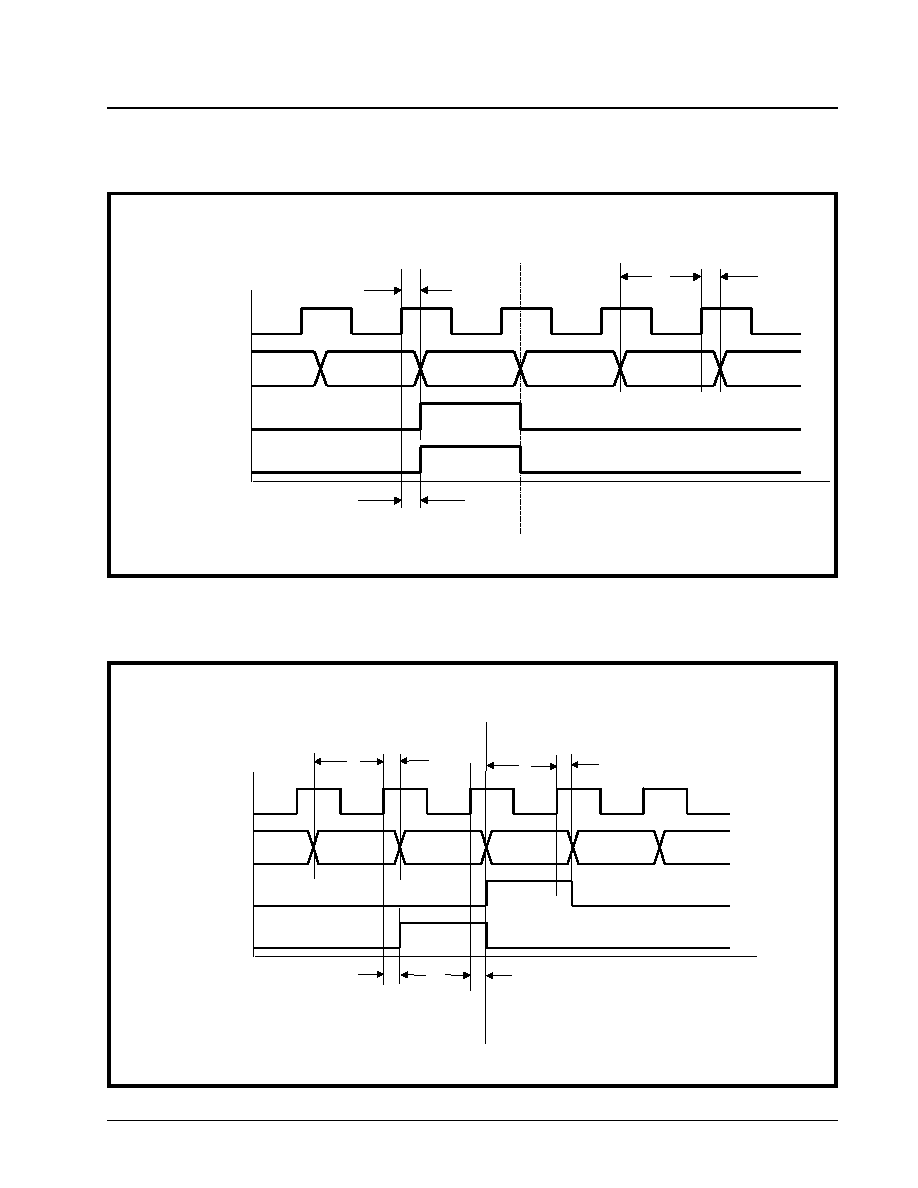
·Á
·Á
·Á
·Á
DS3/E3 FRAMER IC
XRT7250
REV. 1.1.1
25
1.0
TIMING DIAGRAMS
F
IGURE
1. T
IMING
D
IAGRAM
FOR
T
RANSMIT
P
AYLOAD
I
NPUT
I
NTERFACE
,
WHEN
THE
XRT7250 D
EVICE
IS
OPERAT
-
ING
IN
BOTH
THE
DS3
AND
L
OOP
-T
IMING
M
ODES
XRT7250 Transmit Payload Data I/F Signals
RxOutClk
TxSer
TxFrame
TxOH_Ind
Payload[4702]
Payload[4703]
X-Bit
Payload[0]
DS3 Frame Number N
DS3 Frame Number N + 1
t1
t2
t3
t4
F
IGURE
2. T
IMING
D
IAGRAM
FOR
THE
T
RANSMIT
P
AYLOAD
I
NPUT
I
NTERFACE
,
WHEN
THE
XRT7250 D
EVICE
IS
OPER
-
ATING
IN
BOTH
THE
DS3
AND
L
OCAL
-T
IMING
M
ODES
XRT7250 Transmit Payload Data I/F Signals
TxInClk
TxSer
TxFrameRef
TxOH_Ind
Payload[4702]
Payload[4703]
X-Bit
Payload[1]
DS3 Frame Number N
DS3 Frame Number N + 1
t5
t6
t7
t8
t9
t10

XRT7250
DS3/E3 FRAMER IC
·Á
·Á
·Á
·Á
REV. 1.1.1
26
F
IGURE
3. T
IMING
D
IAGRAM
FOR
THE
T
RANSMIT
P
AYLOAD
D
ATA
I
NPUT
I
NTERFACE
,
WHEN
THE
XRT7250 D
EVICE
IS
OPERATING
IN
BOTH
THE
DS3/N
IBBLE
AND
L
OOPED
-T
IMING
M
ODES
RxOutClk
TxNibFrame
TxNibClk
TxNib[3:0]
Nibble [1175]
Nibble [0]
t13
t13A
F
IGURE
4. T
IMING
D
IAGRAM
FOR
THE
T
RANSMIT
P
AYLOAD
D
ATA
I
NPUT
I
NTERFACE
,
WHEN
THE
XRT7250 D
EVICE
IS
OPERATING
IN
THE
DS3/N
IBBLE
AND
L
OCAL
-T
IMING
M
ODES
DS3 Frame Number N
DS3 Frame Number N + 1
TxInClk
TxNibFrame
TxNibClk
TxNib[3:0]
Nibble [1175]
Nibble [0]
Sampling Edge of the XRT7250 Device
t14
t15
TxFrameRef
t16
t17
t18
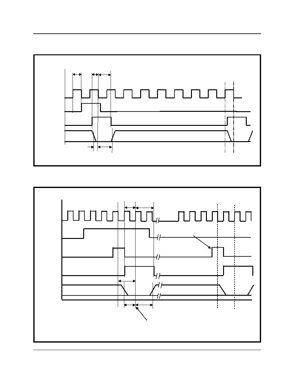
·Á
·Á
·Á
·Á
DS3/E3 FRAMER IC
XRT7250
REV. 1.1.1
27
F
IGURE
5. T
IMING
D
IAGRAM
FOR
THE
T
RANSMIT
O
VERHEAD
D
ATA
I
NPUT
I
NTERFACE
(M
ETHOD
1 A
CCESS
)
TxOHClk
TxOHIns
TxOHFrame
TxOH
Remaining Overhead Bits with DS3 Frame
X bit = 0
X bit = 0
t21
t22
t24
t23
t25
F
IGURE
6. T
IMING
D
IAGRAM
FOR
THE
T
RANSMIT
O
VERHEAD
D
ATA
I
NPUT
I
NTERFACE
(M
ETHOD
2 A
CCESS
)
TxInClk
TxOHFrame
TxOHEnable
TxOHIns
TxOH
XRT7250 samples TxOH
here.
TxOHEnable Pulse # 8
X bit = 0
X bit = 0
t26
t27
t28
t29
t29A
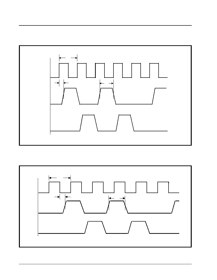
XRT7250
DS3/E3 FRAMER IC
·Á
·Á
·Á
·Á
REV. 1.1.1
28
F
IGURE
7. T
RANSMIT
LIU I
NTERFACE
T
IMING
- F
RAMER
IS
CONFIGURED
TO
UPDATE
"T
X
POS"
AND
"T
X
NEG"
ON
THE
RISING
EDGE
OF
"T
X
L
INE
C
LK
"
TxLineClk
TxPOS
TxNEG
t32
t30
t33
F
IGURE
8. T
RANSMIT
LIU I
NTERFACE
T
IMING
- F
RAMER
IS
CONFIGURED
TO
UPDATE
"T
X
POS"
AND
"T
X
NEG"
ON
THE
FALLING
EDGE
OF
"T
X
L
INE
C
LK
"
TxLineClk
TxPOS
TxNEG
t31
t32
t33
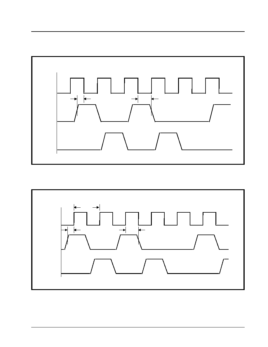
·Á
·Á
·Á
·Á
DS3/E3 FRAMER IC
XRT7250
REV. 1.1.1
29
F
IGURE
9. R
ECEIVE
LIU I
NTERFACE
T
IMING
- F
RAMER
IS
CONFIGURED
TO
SAMPLE
"R
X
POS"
AND
"R
X
NEG"
ON
THE
RISING
EDGE
OF
"R
X
L
INE
C
LK
"
RxLineClk
RxPOS
RxNEG
t40
t41
F
IGURE
10. R
ECEIVER
LIU I
NTERFACE
T
IMING
- F
RAMER
IS
CONFIGURED
TO
SAMPLE
"R
X
POS"
AND
"R
X
NEG"
ON
THE
FALLING
EDGE
OF
"R
X
L
INE
C
LK
"
RxLineClk
RxPOS
RxNEG
t38
t39
t42

XRT7250
DS3/E3 FRAMER IC
·Á
·Á
·Á
·Á
REV. 1.1.1
30
F
IGURE
11. R
ECEIVE
P
AYLOAD
D
ATA
O
UTPUT
I
NTERFACE
T
IMING
X R T 7 2 5 0 R e c e i v e P a y l o a d D a t a I / F S i g n a l s
R x C l k
R x S e r
R x F r a m e
R x O H _ I n d
P a y l o a d [ 4 7 0 2 ]
P a y l o a d [ 4 7 0 3 ]
X - B i t
P a y l o a d [ 0 ]
t 5 0
t 5 1
t 5 2
F
IGURE
12. R
ECEIVE
P
AYLOAD
D
ATA
O
UTPUT
I
NTERFACE
T
IMING
(N
IBBLE
M
ODE
O
PERATION
)
XRT7250 Receive Payload Data I/F Signals
DS3 Frame Number N
DS3 Frame Number N + 1
RxOutClk
RxFrame
RxClk
RxNib[3:0]
Nibble [0]
Nibble [1]
Recommended Sampling Edge of Terminal
Equipment
t53
t54
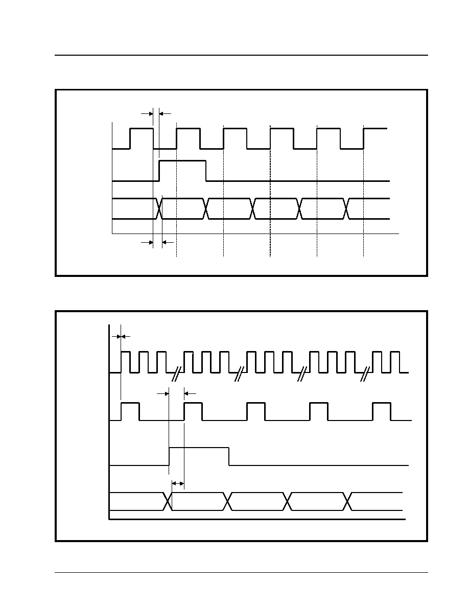
·Á
·Á
·Á
·Á
DS3/E3 FRAMER IC
XRT7250
REV. 1.1.1
31
F
IGURE
13. R
ECEIVE
O
VERHEAD
D
ATA
O
UTPUT
I
NTERFACE
T
IMING
(M
ETHOD
1 - U
SING
R
X
OHC
LK
)
RxOHClk
RxOHFrame
RxOH
X F1 AIC F0 FEAC
t59A
t59B
F
IGURE
14. R
ECEIVE
O
VERHEAD
D
ATA
O
UTPUT
I
NTERFACE
T
IMING
(M
ETHOD
2 - U
SING
R
X
OHE
NABLE
)
RxOutClk
RxOHEnable
RxOHFrame
RxOH
UDL F1 X1 F1 AIC
t60
t60A
t60B
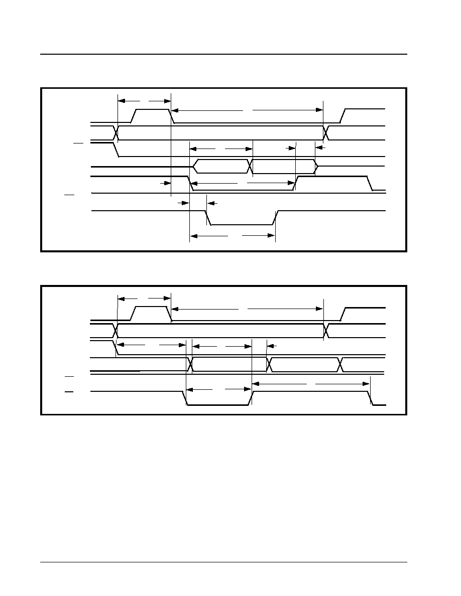
XRT7250
DS3/E3 FRAMER IC
·Á
·Á
·Á
·Á
REV. 1.1.1
32
F
IGURE
15. M
ICROPROCESSOR
I
NTERFACE
T
IMING
- I
NTEL
T
YPE
P
ROGRAMMED
I/O R
EAD
O
PERATIONS
ALE_AS
RDB_DS
A[8:0]
CS
D[15:0]
RDY_DTCK
Not Valid
Valid
Address of Target
WR_RW
t64
t65
t67
t68
t66
t70
t69
t701
F
IGURE
16. M
ICROPROCESSOR
I
NTERFACE
T
IMING
- I
NTEL
T
YPE
P
ROGRAMMED
I/O W
RITE
O
PERATIONS
ALE_AS
A[8:0]
CS*
D[15:0]
WR_RW
Data to be
Address of Target
RD_DS
t64
t65
t71
t72
t73
t66
t770
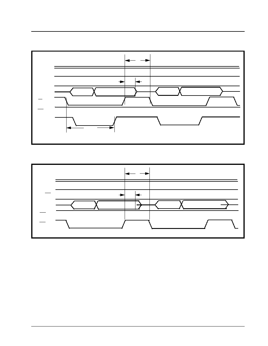
·Á
·Á
·Á
·Á
DS3/E3 FRAMER IC
XRT7250
REV. 1.1.1
33
F
IGURE
17. M
ICROPROCESSOR
I
NTERFACE
T
IMING
- I
NTEL
T
YPE
R
EAD
B
URST
A
CCESS
O
PERATION
ALE_AS
RD_DS
A[8:0]
CS*
D[15:0]
RDY_DTCK
Not Valid
Valid Data at Offset =0x01
WR_RW
Not Valid
Valid Data at Offset =0x02
Address of "Initial" Target Register (Offset = 0x00)
t70
t76
t68
F
IGURE
18. M
ICROPROCESSOR
I
NTERFACE
T
IMING
- I
NTEL
T
YPE
W
RITE
B
URST
A
CCESS
O
PERATION
ALE_AS
A[8:0]
CS
D[15:0]
Not Valid
Valid Data at Offset =0x01
RD_DS
Not Valid
Valid Data at Offset =0x02
WR_RW
Address of "Initial" Target Register (Offset = 0x00)
t76
t68
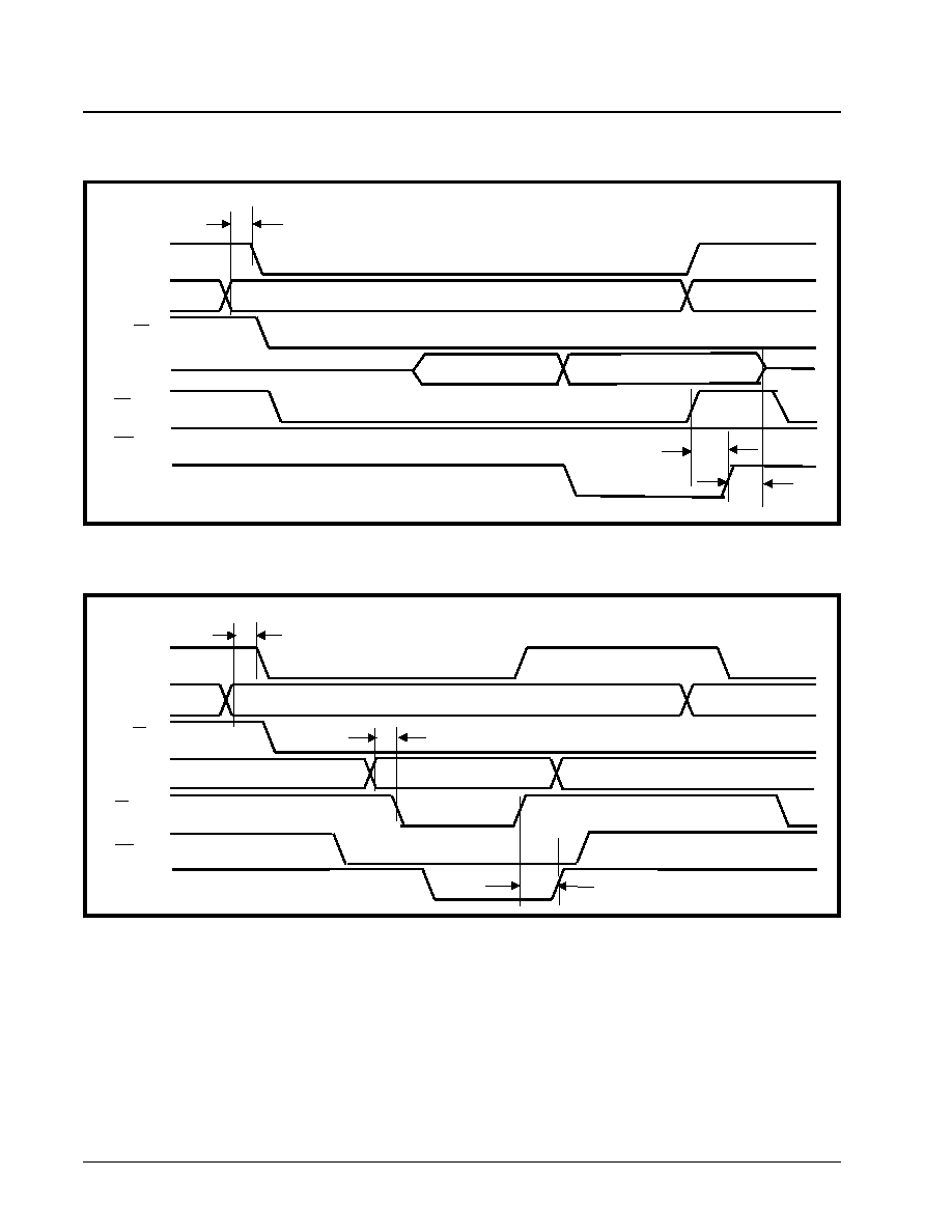
XRT7250
DS3/E3 FRAMER IC
·Á
·Á
·Á
·Á
REV. 1.1.1
34
F
IGURE
19. M
ICROPROCESSOR
I
NTERFACE
T
IMING
- M
OTOROLA
T
YPE
P
ROGRAMMED
I/O R
EAD
O
PERATION
WR_RW
ALE_AS
RD_DS
A[8:0]
CS
D[7:0]
RDY_DTCK
Not Valid
Valid Data
Address of Target Register
t78
t79
t80
F
IGURE
20. M
ICROPROCESSOR
I
NTERFACE
T
IMING
- M
OTOROLA
T
YPE
P
ROGRAMMED
I/O W
RITE
O
PERATION
ALE_AS
A[8:0]
CS
D[7:0]
RD_DS
RDY_DTCK
Data to be Written
Address of Target Register
WR_RW
t78
t82
t81
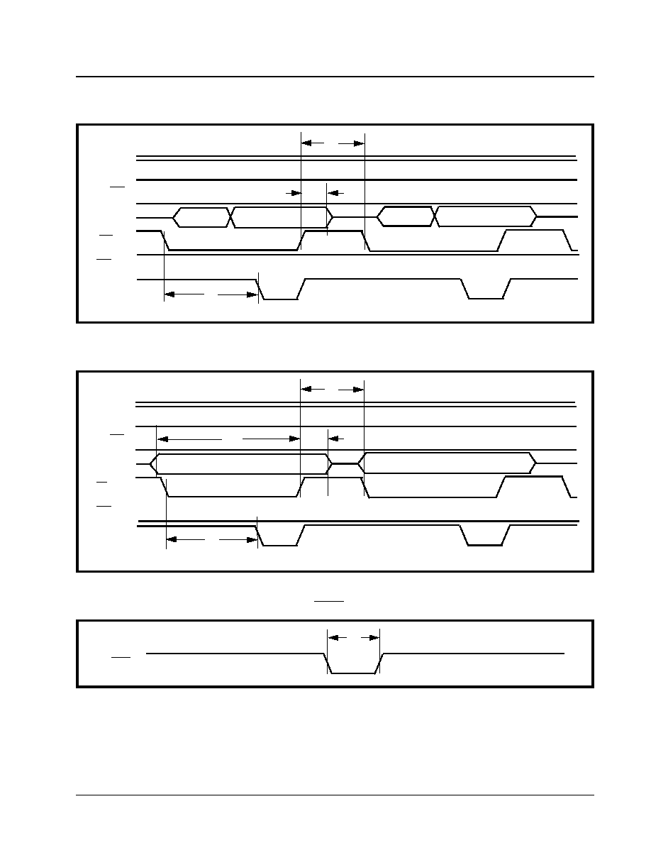
·Á
·Á
·Á
·Á
DS3/E3 FRAMER IC
XRT7250
REV. 1.1.1
35
F
IGURE
21. M
ICROPROCESSOR
I
NTERFACE
T
IMING
- M
OTOROLA
T
YPE
R
EAD
B
URST
A
CCESS
O
PERATION
ALE_AS
RD_DS
A[8:0]
CS
D[15:0]
RDY_DTCK
Not Valid
Valid Data at Offset =0x01
WR_RW
Not Valid
Valid Data at Offset =0x02
Address of "Initial" Target Register (Offset = 0x00)
t81
t88
t82
F
IGURE
22. M
ICROPROCESSOR
I
NTERFACE
T
IMING
- M
OTOROLA
T
YPE
W
RITE
B
URST
A
CCESS
O
PERATION
ALE_AS
RD_DS
A[8:0]
CS
D[15:0]
RDY_DTCK
Data Written at Offset =0x01
WR_RW
Data Written at Offset =0x02
Address of "Initial" Target Register (Offset = 0x00)
t81
t85
t89
t84
F
IGURE
23. M
ICROPROCESSOR
I
NTERFACE
T
IMING
- R
ESET
P
ULSE
W
IDTH
Reset
t90
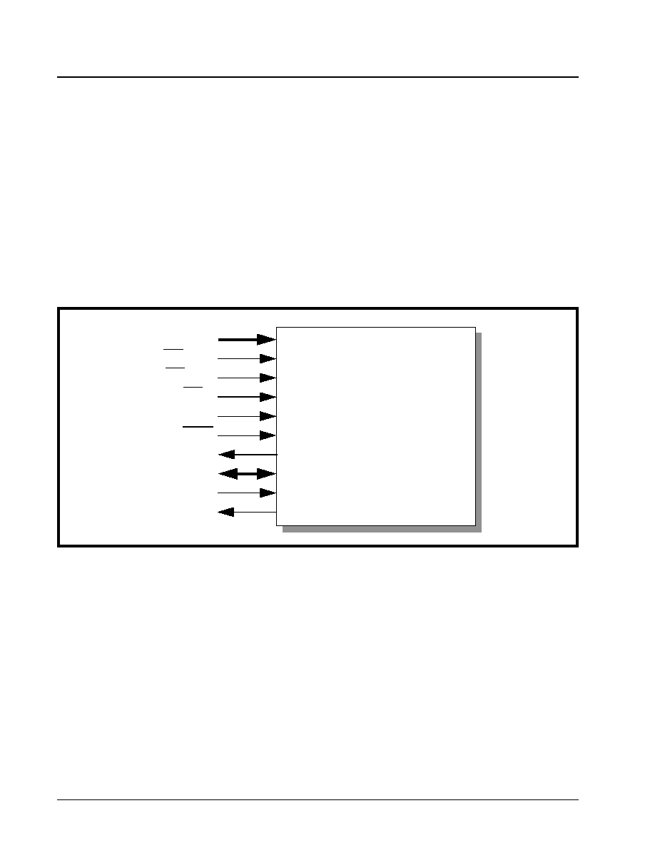
XRT7250
DS3/E3 FRAMER IC
·Á
·Á
·Á
·Á
REV. 1.1.1
36
2.0
THE MICROPROCESSOR INTERFACE
BLOCK
The Microprocessor Interface section supports com-
munication between the local microprocessor (µP)
and the Framer IC. In particular, the Microprocessor
Interface section supports the following operations
between the local microprocessor and the Framer.
∑ The writing of configuration data into the Framer
on-chip (addressable) registers.
∑ The writing of an outbound PMDL (Path Mainte-
nance Data Link) message into the Transmit LAPD
Message buffer (within the Framer IC).
∑ The Framer IC's generation of an Interrupt Request
to the µP.
∑ The µP's servicing of the interrupt request from the
Framer IC.
∑ The monitoring of the system's health by periodi-
cally reading the on-chip Performance Monitor reg-
isters.
∑ The reading of an inbound PMDL Message from
the Receive LAPD Message Buffer (within the
Framer IC).
Each of these operations (between the local micro-
processor and the Framer IC) will be discussed in
some detail, throughout this data sheet.
Figure 24 presents a simple block diagram of the Mi-
croprocessor Interface Section, within the Framer IC.
2.1
T
HE
M
ICROPROCESSOR
I
NTERFACE
B
LOCK
S
IG
-
NAL
The Framer IC may be configured into a wide variety
of different operating modes and have its perfor-
mance monitored by software through a standard (lo-
cal housekeeping) microprocessor, using data, ad-
dress and control signals.
The local µP configures the Framer IC (into a desired
operating mode) by writing data into specific address-
able, on-chip Read/Write registers, or on-chip RAM.
The microprocessor interface provides the signals
which are required for a general purpose micropro-
cessor to read or write data into these registers. The
Microprocessor Interface also supports polled and in-
terrupt driven environments. These interface signals
are described below in Table 1, Table 2, and Table 3.
The microprocessor interface can be configured to
operate in the Motorola Mode or in the Intel mode.
When the Microprocessor Interface is operating in the
Motorola mode, then some of the control signals
function in a manner as required by the Motorola
68000 family of microprocessors. Likewise, when the
Microprocessor Interface is operating in the Intel
Mode, then some of these Control Signals function in
a manner as required by the Intel 80xx family of mi-
croprocessors.
Table 1 lists and describes those Microprocessor In-
terface signals whose role is constant across the two
modes. Table 2 describes the role of some of these
signals when the Microprocessor Interface is operat-
ing in the Intel Mode. Likewise, Table 3 describes the
role of these signals when the Microprocessor Inter-
face is operating in the Motorola Mode.
F
IGURE
24. S
IMPLE
B
LOCK
D
IAGRAM
OF
THE
M
ICROPROCESSOR
I
NTERFACE
B
LOCK
,
WITHIN
THE
F
RAMER
IC
A[8:0]
WR_RW
Rd_DS
CS
ALE_AS
Reset
Int
D[7:0]
MOTO
RDY_DTCK
Microprocessor
and
Programmable

·Á
·Á
·Á
·Á
DS3/E3 FRAMER IC
XRT7250
REV. 1.1.1
37
T
ABLE
1: D
ESCRIPTION
OF
THE
M
ICROPROCESSOR
I
NTERFACE
S
IGNALS
THAT
EXHIBIT
CONSTANT
ROLES
IN
BOTH
THE
I
NTEL
AND
M
OTOROLA
M
ODES
P
IN
N
AME
T
YPE
D
ESCRIPTION
MOTO
I
Selection input for Intel/Motorola µP Interface.
Setting this pin to a logic "High" configures the Microprocessor Interface to operate in the Motorola
mode. Likewise, setting this pin to a logic "Low" configures the Microprocessor Interface to operate
in the Intel Mode.
D[7:0]
I/O
Bi-Directional Data Bus for register read or write operations
A[8:0]
I
Nine Bit Address Bus input:
This nine bit Address Bus is provided to allow the user to select an on-chip register or on-chip RAM
location.
CS
I
Chip Select input.
This "active low" signal selects the Microprocessor Interface of the UNI device and enables read/
write operations with the on-chip registers/on-chip RAM.
Int
O
Interrupt Request Output:
This open-drain/active-low output signal will inform the local
µP
that the UNI has an interrupt condi-
tion that needs servicing.
T
ABLE
2: P
IN
D
ESCRIPTION
OF
M
ICROPROCESSOR
I
NTERFACE
S
IGNALS
- W
HILE
THE
M
ICROPROCESSOR
I
NTERFACE
IS
O
PERATING
IN
THE
I
NTEL
M
ODE
P
IN
N
AME
E
QUIVALENT
P
IN
IN
I
NTEL
ENVIRONMENT
T
YPE
D
ESCRIPTION
ALE_AS
ALE
I
Address-Latch Enable: This "active-high" signal is used to latch the contents on
the address bus, A[8:0]. The contents of the Address Bus are latched into the
A[8:0] inputs on the falling edge of ALE_AS. Additionally, this signal can be used
to indicate the start of a burst cycle.
RD_DS
RD*
I
Read Signal: This "active-low" input functions as the read signal from the local
µP
. When this signal goes "Low", the UNI Microprocessor Interface will place the
contents of the addressed register on the Data Bus pins (D[15:0]). The Data Bus
will be "tri-stated" once this input signal returns "High".
WR_RW
WR*
I
Write Signal: This "active-low" input functions as the write signal from the local
µP
. The contents of the Data Bus (D[15:0]) will be written into the addressed reg-
ister (via A[8:0]), on the rising edge of this signal.
RDY_DTCK
READY*
O
Ready Output: This "active-low" signal is provided by the UNI device, and indi-
cates that the current read or write cycle is to be extended until this signal is
asserted. The local
µP
will typically insert WAIT states until this signal is
asserted. This output will toggle "Low" when the device is ready for the next
Read or Write cycle.

XRT7250
DS3/E3 FRAMER IC
·Á
·Á
·Á
·Á
REV. 1.1.1
38
2.2
I
NTERFACING
THE
XRT7250 DS3/E3 F
RAMER
TO
THE
L
OCAL
µC/µP
VIA
THE
M
ICROPROCESSOR
I
NTERFACE
B
LOCK
The Microprocessor Interface block, within the Fram-
er device is very flexible and provides the following
options to the user.
∑ To interface the Framer device to a µC/µP over an
8-bit wide bi-directional data bus.
∑ To interface the Framer to an Intel-type or Motorola-
type µC/µP.
∑ To transfer data (between the Framer IC and the
µC/µP) via the Programmed I/O or Burst Mode
Each of the options are discussed in detail below.
Section 3.2.1 will discussed the issues associated
with interfacing the Framer to a µC/µP over an 8-bit
bi-directional data bus. Afterwards, Section 3.2.2 will
discuss Data Access (e.g., Programmed I/O and
Burst) Mode when interfaced to both Motorola-type
and Intel-type µC/µP.
2.2.1
Interfacing the XRT7250 DS3/E3 Framer
to the Microprocessor over an 8 bit wide bi-direc-
tional Data Bus
The XRT7250 DS3/E3 Framer Microprocessor Inter-
face permits the user to interface it to a µC/µP over an
8-bit wide bi-directional data bus.
2.2.1.1
Interfacing the Framer to the µC/µP
over an 8-bit wide bi-directional data bus.
In general, interfacing the Framer to an 8-bit µC/µP is
quite straight-forward. This is because most of the
registers, within the Framer, are 8-bits wide. Further,
in this mode, the µC/µP can read or write data into
both even and odd numbered addresses within the
Framer address space.
Reading Performance Monitor (PMON) Registers
The only awkward issue that the user should be wary
of (while operating in the 8-bit mode) occurs whenev-
er the µC/µP needs to read the contents of one of the
PMON (Performance Monitor) registers.
The XRT7250 DS3/E3 Framer Device consists of the
following PMON Registers.
∑ PMON LCV Event Count Register
∑ PMON Framing Error Event Count Register
∑ PMON Received FEBE Event Count Register
∑ PMON Parity Error Event Count Register
∑ PMON Received Single-Bit HEC Error Count Reg-
ister
∑ PMON Received Multiple-Bit HEC Error Count
Register
∑ PMON Received Idle Cell Count Register
∑ PMON Received Valid Cell Count Register
∑ PMON Discarded Cell Count Register
∑ PMON Transmitted Idle Cell Count Register
∑ PMON Transmitted Valid Cell Count Register.
Unlike most of the registers within the Framer, the
PMON registers are 16-bit registers (or 16-bits wide).
Table 4 lists each of these PMON registers as con-
sisting of two 8-bit registers. One of these 8-bit regis-
ter is labeled MSB (or Most Significant Byte) and the
other register is labeled LSB (or Least Significant
T
ABLE
3: P
IN
D
ESCRIPTION
OF
THE
M
ICROPROCESSOR
I
NTERFACE
S
IGNALS
WHILE
THE
M
ICROPROCESSOR
I
NTERFACE
IS
OPERATING
IN
THE
M
OTOROLA
M
ODE
P
IN
N
AME
E
QUIVALENT
P
IN
IN
M
OTOROLA
ENVIRONMENT
T
YPE
D
ESCRIPTION
ALE_AS
AS*
I
Address Strobe: This "active-low" signal is used to latch the contents on the
address bus input pins: A[8:0] into the Microprocessor Interface circuitry. The
contents of the Address Bus are latched into the UNI device on the rising edge of
the ALE_AS signal. This signal can also be used to indicate the start of a burst
cycle.
RD_DS
DS*
I
Data Strobe: This signal latches the contents of the bi-directional data bus pins
into the Addressed Register (within the UNI) during a Write Cycle.
WR_RW
R/W*
I
Read/Write* Input: When this pin is "High", it indicates a Read Cycle. When this
pin is "Low", it indicates a Write cycle.
RDY_DTCK
DTACK*
O
Data Transfer Acknowledge: The UNI device asserts DTACK* in order to inform
the CPU that the present READ or WRITE cycle is nearly complete. The 68000
family of CPUs requires this signal from its peripheral devices, in order to quickly
and properly complete a READ or WRITE cycle.

·Á
·Á
·Á
·Á
DS3/E3 FRAMER IC
XRT7250
REV. 1.1.1
39
Byte). When an 8-bit PMON Register is concatenat-
ed with its companion 8-bit PMON Register, one ob-
tains the full 16-bit expression within that PMON Reg-
ister.
The consequence of having these 16-bit registers is
that an 8-bit µC/µP will have to perform two consecu-
tive read operations in order to read in the full 16-bit
expression contained within a given PMON register.
To complicate matters, these PMON Registers are
Reset-Upon-Read registers. More specifically, these
PMON Register are Reset-Upon-Read in the sense
that, the entire 16-bit contents, within a given PMON
Register is reset, as soon as an 8-bit µC/µP reads in
either byte of this two-byte (e.g., 16 bit) expression.
For example;
Consider that an 8-bit µC/µP needs to read in the
PMON LCV Event Count Register. In order to ac-
complish this task, the 8-bit µC/µP is going to have to
read in the contents of PMON LCV Event Count Reg-
ister - MSB (located at Address = 0x50) and the con-
tents of the PMON LCV Event Count Register - LSB
(located at Address = 0x51). These two eight-bit reg-
isters, when concatenated together, make up the
PMON LCV Event Count Register.
If the 8-bit µC/µP reads in the PMON LCV Event
Count-LSB register first, then the entire PMON LCV
Event Count register will be reset to 0x0000. As a
consequence, if the 8-bit µC/µP attempts to read in
the PMON LCV Event Count-MSB register in the very
next read cycle, it will read in the value 0x00.
The PMON Holding Register
In order to resolve this Reset-Upon-Read problem,
the XRT7250 DS3/E3 Framer device includes a spe-
cial register, which permits 8-bit µC/µP to read in the
full 16-bit contents of these PMON registers. This
special register is called the PMON Holding Register
and is located at 0x6c within the Framer Address
space.
The operation of the PMON Holding register is as fol-
lows. Whenever an 8-bit µC/µP reads in one of the
bytes (of the 2-byte PMON register), the contents of
the unread (e.g., other) byte will be stored in the
PMON Holding Register. Therefore, the 8-bit µC/µP
must then read in the contents of the PMON Holding
Register in the very next read operation.
In Summary: Whenever an 8-bit
µC/µP
needs to
read a PMON Register, it must execute the follow-
ing steps.
Step 1: Read in the contents of a given 8-bit PMON
Register (it does not matter whether the µC/µP reads
in the MSB or the LSB register).
Step 2: Read in the contents of the PMON Holding
Register (located at Address = 0x6c). This register
will contain the contents of the other byte.
2.2.2
Data Access Modes
As mentioned earlier, the Microprocessor Interface
block supports data transfer between the Framer and
the µC/µP (e.g., Read and Write operations) via two
modes: the Programmed I/O and the Burst Modes.
Each of these Data Access Modes are discussed in
detail below.
2.2.2.1
Data Access using Programmed I/O
Programmed I/O is the conventional manner in which
a microprocessor exchanges data with a peripheral
device. However, it is also the slowest method of data
exchange between the Framer and the µC/µP.
The next two sections present detailed information on
Programmed I/O Access, when the XRT7250 DS3/E3
Framer is operating in the Intel Mode or in the Motor-
ola Mode.
2.2.2.1.1
Programmed I/O Access in the Intel
Mode
If the XRT7250 DS3/E3 Framer is interfaced to an In-
tel-type µC/µP (e.g., the 80x86 family, etc.), then it
should be configured to operate in the Intel mode (by
tying the MOTO pin to ground). Intel-type Read and
Write operations are described below.
2.2.2.1.1.1
The Intel Mode Read Cycle
Whenever an Intel-type µC/µP wishes to read the
contents of a register or some location within the Re-
ceive LAPD Message buffer or the Receive OAM Cell
Buffer, (within the Framer device), it should do the fol-
lowing.
1. Place the address of the target register or buffer
location (within the Framer) on the Address Bus
input pins A[8:0].
2. While the µC/µP is placing this address value on
the Address Bus, the Address Decoding circuitry
(within the user's system) should assert the CS
(Chip Select) pin of the Framer, by toggling it
"Low". This action enables further communica-
tion between the µC/µP and the Framer Micropro-
cessor Interface block.
3. Toggle the ALE_AS (Address Latch Enable) input
pin "High". This step enables the Address Bus
input drivers, within the Microprocessor Interface
block of the Framer.
4. After allowing the data on the Address Bus pins
to settle (by waiting the appropriate Address Data
Setup time), the µC/µP should toggle the
ALE_AS pin "Low". This step causes the Framer
device to latch the contents of the Address Bus
into its internal circuitry. At this point, the address

XRT7250
DS3/E3 FRAMER IC
·Á
·Á
·Á
·Á
REV. 1.1.1
40
of the register or buffer locations (within the
Framer), has now been selected.
5. Next, the µC/µP should indicate that this current
bus cycle is a Read Operation by toggling the
RD_DS (Read Strobe) input pin "Low". This
action also enables the bi-directional data bus
output drivers of the Framer device. At this point,
the bi-directional data bus output drivers will pro-
ceed to drive the contents of the latched
addressed register (or buffer location) onto the bi-
directional data bus, D[7:0].
6. Immediately after the µC/µP toggles the Read
Strobe signal "Low", the Framer device will toggle
the RDY_DTCK output pin "Low". The Framer
device does this in order to inform the µC/µP that
the data (to be read from the data bus) is NOT
READY to be latched into the µC/µP.
7. After some settling time, the data on the bi-direc-
tional data bus will stabilize and can be read by
the µC/µP. The XRT7250 DS3/E3 Framer will
indicate that this data can be read by toggling the
RDY_DTCK (READY) signal "High".
8. After the µC/µP detects the RDY_DTCK signal
(from the XRT7250 DS3/E3 Framer), it can then
terminate the Read Cycle by toggling the RD_DS
(Read Strobe) input pin "High".
Figure 25 presents a timing diagram which illustrates
the behavior of the Microprocessor Interface signals,
during an Intel-type Programmed I/O Read Opera-
tion.
2.2.2.1.1.2
The Intel Mode Write Cycle
Whenever an Intel-type µC/µP wishes to write a byte
or word of data into a register or buffer location, within
the Framer, it should do the following.
1. Assert the ALE_AS (Address Latch Enable) input
pin by toggling it "High". When the µC/µP asserts
the ALE_AS input pin, it enables the Address Bus
Input Drivers within the Framer chip.
2. Place the address of the target register or buffer
location (within the Framer), on the Address Bus
input pins, A[8:0].
3. While the µC/µP is placing this address value
onto the Address Bus, the Address Decoding cir-
cuitry (within the user's system) should assert the
CS input pin of the Framer device by toggling it
"Low". This step enables further communication
between the µC/µP and the Framer Microproces-
sor Interface block.
4. After allowing the data on the Address Bus pins
to settle (by waiting the appropriate Address
Setup time), the µC/µP should toggle the
ALE_AS input pin "Low". This step causes the
Framer device to latch the contents of the
Address Bus into its internal circuitry. At this
point, the address of the register or buffer loca-
tion (within the Framer), has now been selected.
5. Next, the µC/µP should indicate that this current
bus cycle is a Write Operation by toggling the
WR_RW (Write Strobe) input pin "Low". This
action also enables the bi-directional data bus
input drivers of the Framer device.
6. The µC/µP should then place the byte or word
that it intends to write into the target register, on
the bi-directional data bus, D[7:0].
7. After waiting the appropriate amount of time for
the data (on the bi-directional data bus) to settle,
the µC/µP should toggle the WR_RW (Write
F
IGURE
25. B
EHAVIOR
OF
M
ICROPROCESSOR
I
NTERFACE
SIGNALS
DURING
AN
I
NTEL
-
TYPE
P
ROGRAMMED
I/O R
EAD
O
PERATION
ALE_AS
RD_DS
A[8:0]
CS
D[15:0]
RDY_DTCK
Not Valid
Valid
Address of Target Register
WR_RW
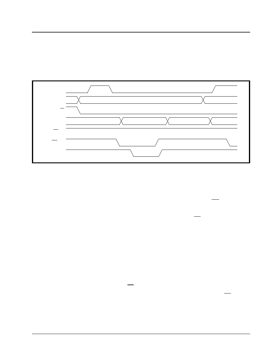
·Á
·Á
·Á
·Á
DS3/E3 FRAMER IC
XRT7250
REV. 1.1.1
41
Strobe) input pin "High". This action accom-
plishes two things:
a. It latches the contents of the bi-directional data
bus into the XRT7250 DS3/E3 Framer Micropro-
cessor Interface block.
b. It terminates the write cycle.
Figure 26 presents a timing diagram which illustrates
the behavior of the Microprocessor Interface signals,
during an Intel-type Programmed I/O Write Opera-
tion.
2.2.2.1.2
Programmed I/O Access in the Motor-
ola Mode
If the XRT7250 DS3/E3 Framer is interfaced to a Mo-
torola-type µC/µP (e.g., the MC680X0 family, etc.), it
should be configured to operate in the Motorola mode
(by tying the MOTO pin to Vcc). Motorola-type Pro-
grammed I/O Read and Write operations are de-
scribed below.
2.2.2.1.2.1
The Motorola Mode Read Cycle
Whenever a Motorola-type µC/µP wishes to read the
contents of a register or some location within the Re-
ceive LAPD Message or Receive OAM Cell Buffer,
(within the Framer device) it should do the following.
1. Assert the ALE_AS (Address-Strobe) input pin by
toggling it low. This step enables the Address
Bus input drivers, within the Microprocessor Inter-
face Block of the Framer IC.
2. Place the address of the target register (or buffer
location) within the Framer, on the Address Bus
input pins, A[8:0].
3. At the same time, the Address Decoding circuitry
(within the user's system) should assert the CS
(Chip Select) input pin of the Framer device, by
toggling it "Low". This action enables further
communication between the µC/µP and the
Framer Microprocessor Interface block.
4. After allowing the data on the Address Bus pins
to settle (by waiting the appropriate Address
Setup time), the µC/µP should toggle the
ALE_AS input pin "High". This step causes the
Framer device to latch the contents of the
Address Bus into its internal circuitry. At this
point, the address of the register or buffer loca-
tion (within the Framer) has now been selected.
5. Further, the µC/µP should indicate that this cycle
is a Read cycle by setting the WR_RW (R/W*)
input pin "High".
6. Next the µC/µP should initiate the current bus
cycle by toggling the RD_DS (Data Strobe) input
pin "Low". This step enables the bi-directional
data bus output drivers, within the XRT7250 DS3/
E3 Framer device. At this point, the bi-directional
data bus output drivers will proceed to driver the
contents of the Address register onto the bi-direc-
tional data bus, D[7:0].
7. After some settling time, the data on the bi-direc-
tional data bus will stabilize and can be read by
the µC/µP. The XRT7250 DS3/E3 Framer will
indicate that this data can be read by asserting
the RDY_DTCK (DTACK) signal.
8. After the µC/µP detects the RDY_DTCK signal
(from the XRT7250 DS3/E3 Framer) it will termi-
nate the Read Cycle by toggling the RD_DS
(Data Strobe) input pin "High".
Figure 27 presents a timing diagram which illustrates
the behavior of the Microprocessor Interface signals
during a Motorola-type Programmed I/O Read Opera-
tion.
F
IGURE
26. B
EHAVIOR
OF
THE
M
ICROPROCESSOR
I
NTERFACE
S
IGNALS
,
DURING
AN
I
NTEL
-
TYPE
P
ROGRAMMED
I/O
W
RITE
O
PERATION
ALE_AS
A[8:0]
CS
D[7:0]
RD_DS
WR_RW
RDY_DTCK
Address of Target Register
Data to be written
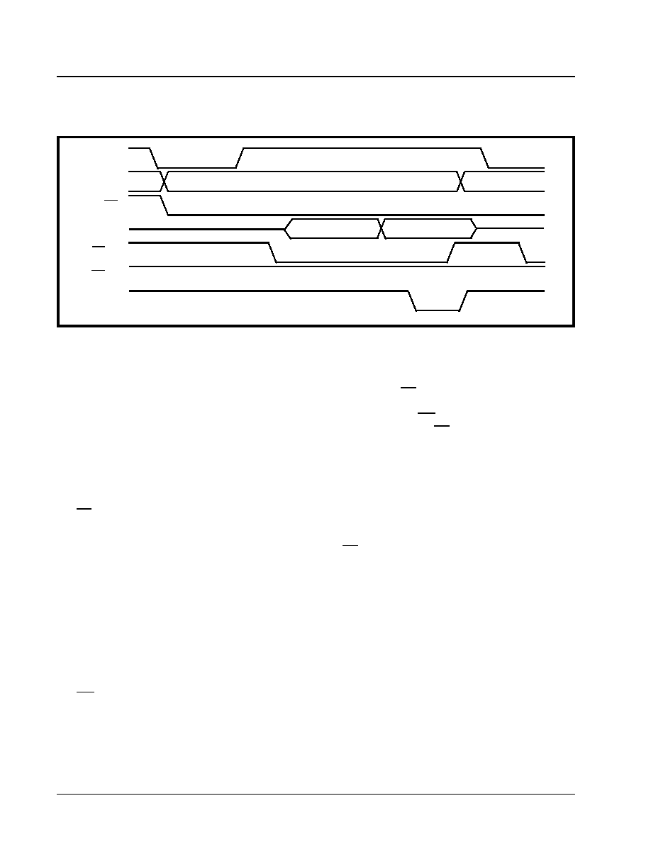
XRT7250
DS3/E3 FRAMER IC
·Á
·Á
·Á
·Á
REV. 1.1.1
42
2.2.2.1.2.2
The Motorola Mode Write Cycle
Whenever a Motorola-type µC/µP wishes to write a
byte or word of data into a register or buffer location,
within the Framer, it should do the following.
1. Assert the ALE_AS (Address Select) input pin by
toggling it "Low". This step enables the Address
Bus input drivers (within the Framer chip).
2. Place the address of the target register or buffer
location (within the Framer), on the Address Bus
input pins, A[8:0].
3. While the µC/µP is placing this address value
onto the Address Bus, the Address-Decoding cir-
cuitry (within the user's system) should assert the
CS (Chip Select) input pins of the Framer by tog-
gling it "Low". This step enables further commu-
nication between the µC/µP and the Framer
Microprocessor Interface block.
4. After allowing the data on the Address Bus pins
to settle (by waiting the appropriate Address
Setup time), the µC/µP should toggle the
ALE_AS input pin "High". This step causes the
Framer device to latch the contents of the
Address Bus into its own circuitry. At this point,
the Address of the register or buffer location
(within the Framer), has now been selected.
5. Further, the µC/µP should indicate that this cur-
rent bus cycle is a Write operation by toggling the
WR_RW (R/W*) input pin "Low".
6. The µC/µP should then place the byte or word
that it intends to write into the target register, on
the bi-directional data bus, D[7:0].
7. Next, the µC/µP should initiate the bus cycle by
toggling the RD_DS (Data Strobe) input pin
"Low". When the XRT7250 DS3/E3 Framer
senses that the WR_RW (R/W*) input pin is
"High" and that the RD_DS (Data Strobe) input
pin has toggled "Low", it will enable the input driv-
ers of the bi-directional data bus, D[7:0].
8. After waiting the appropriate time, for this newly
placed data to settle on the bi-directional data
bus (e.g., the Data Setup time) the Framer will
assert the RDY_DTCK output signal.
9. After the µC/µP detects the RDY_DTCK signal
(from the Framer), the µC/µP should toggle the
RD_DS input pin "High". This action accom-
plishes two things.
a. It latches the contents of the bi-directional data
bus into the XRT7250 DS3/E3 Microprocessor
Interface block.
b. It terminates the Write cycle.
Figure 28 presents a timing diagram which illustrates
the behavior of the Microprocessor Interface signals,
during a Motorola-type Programmed I/O Write Opera-
tion.
F
IGURE
27. I
LLUSTRATION
OF
THE
B
EHAVIOR
OF
M
ICROPROCESSOR
I
NTERFACE
SIGNALS
,
DURING
A
M
OTOROLA
-
TYPE
P
ROGRAMMED
I/O R
EAD
O
PERATION
ALE_AS
RD_DS
A[8:0]
CS
D[15:0]
RDY_DTCK
Not Valid
Valid Data
Address of Target Register
WR_RW
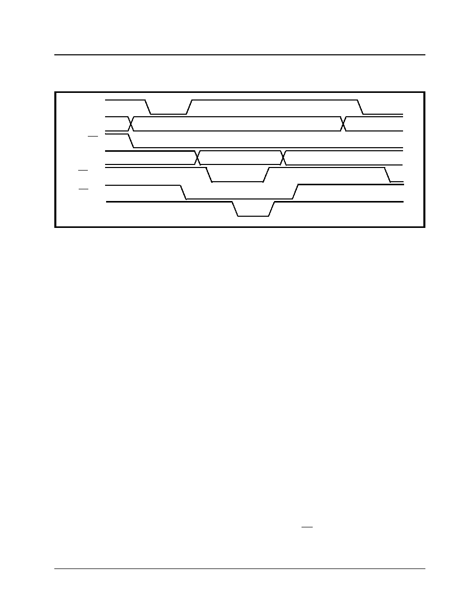
·Á
·Á
·Á
·Á
DS3/E3 FRAMER IC
XRT7250
REV. 1.1.1
43
2.2.2.2
Data Access using Burst Mode I/O
Burst Mode I/O access is a much faster way to trans-
fer data between the µC/µP and the Microprocessor
Interface (of the XRT7250 DS3/E3 Framer), than Pro-
grammed I/O. The reason why Burst Mode I/O is
faster is explained below.
Data is placed upon the Address Bus input pins
A[8:0] only for the very first access, within a given
burst access. The remaining read or write operations
(within this burst access) do not require the place-
ment of the Address Data on the Address Data Bus.
As a consequence, the user does not have to wait
through the Address Setup and Hold times for each of
these Read/Write operation, within the Burst Access.
It is important to note that there are some limitations
associated with Burst Mode I/O Operations.
1. All cycles within the Burst Access, must be either
all Read or all Write cycles. No mixing of Read
and Write cycles is permitted.
2. A Burst Access can only be used when Read or
Write operations are to be employed over a con-
tiguous range of address locations, within the
Framer device.
3. The very first Read or Write cycle, within a burst
access, must start at the lowest address value, of
the range of addresses to be accessed. Subse-
quent operations will automatically be incre-
mented to the very next higher address value.
Examples of Burst Mode I/O operations are present-
ed below for read and write operations, with both In-
tel-type and Motorola-type µC/µP.
2.2.2.2.1
Burst I/O Access in the Intel Mode
If the XRT7250 DS3/E3 Framer is interfaced to an In-
tel-type µC/µP (e.g., the 80x86 family, etc.), then it
should be configured to operate in the Intel mode (by
tying the MOTO pin to ground). Intel-type Read and
Write Burst I/O Access operations are described be-
low.
2.2.2.2.1.1
The Intel-Mode Read Burst Access
Whenever an Intel-type µC/µP wishes to read the
contents of numerous registers or buffer locations
over a contiguous range of addresses, then it should
do the following.
a. Perform the initial read operation of the burst
access.
b. Perform the remaining read operations of the
burst access.
c. Terminate the burst access operation.
Each of these operations within the burst access are
described below.
2.2.2.2.1.1.1
The Initial Read Operation
The initial read operation of an Intel-type read burst
access is accomplished by executing a Programmed
I/O Read Cycle as summarized below.
A.0
Execute a Single Ordinary (Programmed I/
O) Read Cycle, as described in steps A.1
through A.7 below.
A.1
Place the address of the initial-target register or
buffer location (within the Framer) on the
Address Bus input pins A[8:0].
A.2
While the µC/µP is placing this address value
onto the Address Bus, the Address Decoding
circuitry (within the user's system) should
assert the CS input pin of the Framer, by tog-
gling it "Low". This step enables further com-
F
IGURE
28. I
LLUSTRATION
OF
THE
B
EHAVIOR
OF
THE
M
ICROPROCESSOR
I
NTERFACE
SIGNAL
,
DURING
A
M
OTOROLA
-
TYPE
P
ROGRAMMED
I/O W
RITE
O
PERATION
ALE_AS
A[8:0]
CS
D[15:0]
RD_DS
RDY_DTCK
Data to be Written
Address of Target Register
WR_RW
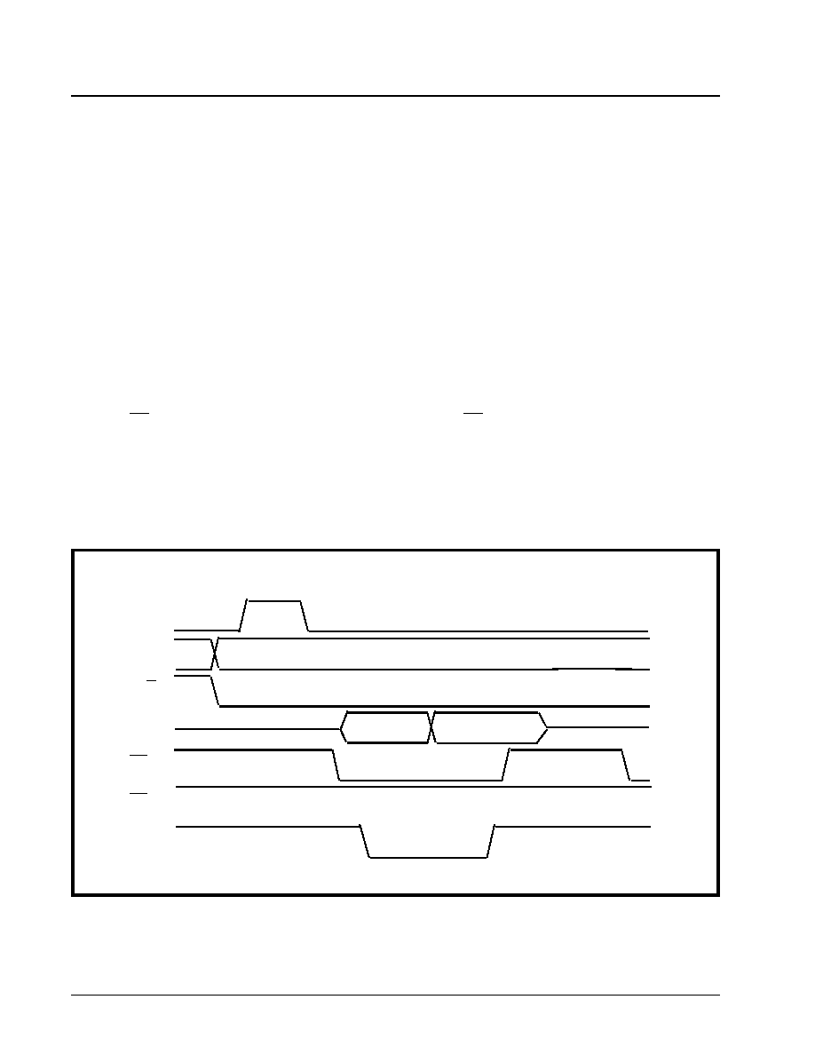
XRT7250
DS3/E3 FRAMER IC
·Á
·Á
·Á
·Á
REV. 1.1.1
44
munication between the µC/µP and the Framer
Microprocessor Interface block.
A.3
Assert the ALE_AS (Address Latch Enable) pin
by toggling it "High". This step enables the
Address Bus input drivers, within the Micropro-
cessor Interface block of the Framer.
A.4
After allowing the data on the Address Bus pins
to settle (by waiting the appropriate Address
Data Setup time), the µC/µP should then toggle
the ALE_AS pin "Low". This step latches the
contents, on the Address Bus pins, A[8:0], into
the XRT7250 DS3/E3 Framer Microprocessor
Interface block. At this point, the initial address
of the burst access has now been selected.
N
OTE
: The ALE_AS input pin should remain "Low" for the
remainder of this Burst Access operation.
A.5
Next, the µC/µP should indicate that this cur-
rent bus cycle is a Read Operation by toggling
the RD_DS (Read Strobe) input pin "Low".
This action also enables the bi-directional data
bus output drivers of the Framer device. At this
point, the bi-directional data bus output drivers
will proceed to drive the contents of the
addressed register onto the bi-directional data
bus, D[7:0].
A.6
Immediately after the µC/µP toggles the Read
Strobe signal "Low", the Framer device will tog-
gle the RDY_DTCK (READY) output pin "Low".
The Framer device does this in order to inform
the µC/µP that the data (to be read from the
data bus) is NOT READY to be latched into the
µC/µP.
A.7
After some settling time, the data on the bi-
directional data bus will stabilize and can be
read by the µC/µP. The XRT7250 DS3/E3
Framer will indicate that this data is ready to be
read, by toggling the RDY_DTCK (Ready) sig-
nal "High".
A.8
After the µC/µP detects the RDY_DTCK signal
(from the XRT7250 DS3/E3 Framer IC), it can
then will terminate the Read cycle by toggling
the RD_DS (Read Strobe) input pin "High".
Figure 29 presents an illustration of the behavior of
the Microprocessor Interface Signals, during the initial
Read Operation, within a Burst I/O Cycle for an Intel-
type µC/µP.
At the completion of this initial read cycle, the µC/µP
has read in the contents of the first register or buffer
location (within the XRT7250 DS3/E3 Framer) for this
particular burst I/O access operation. In order to illus-
trate how this burst access operation works, the byte
(or word) of data, that is being read in Figure 29, has
been labeled Valid Data at Offset = 0x00. This label
F
IGURE
29. B
EHAVIOR
OF
THE
M
ICROPROCESSOR
I
NTERFACE
S
IGNALS
,
DURING
THE
I
NITIAL
R
EAD
O
PERATION
OF
A
B
URST
C
YCLE
(I
NTEL
T
YPE
P
ROCESSOR
)
ALE_AS
RD_DS
A[8:0]
CS
D[15:0]
RDY_DTCK
Not Valid
Valid Data of Offset = 0x00
Address of "Initial" Target Register (Offset = 0x00)
WR_RW
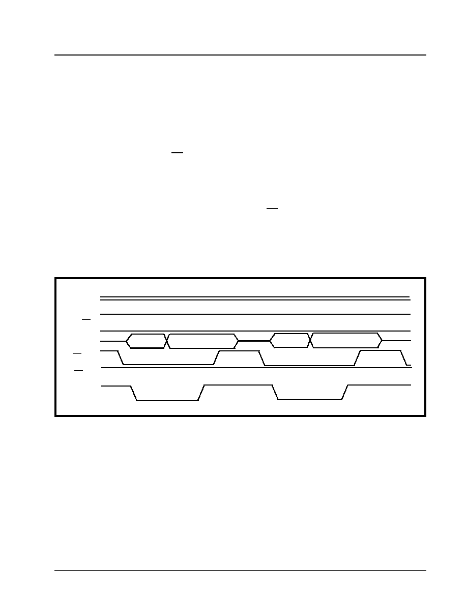
·Á
·Á
·Á
·Á
DS3/E3 FRAMER IC
XRT7250
REV. 1.1.1
45
indicates that the µC/µP is reading the very first regis-
ter (or buffer location) in this burst access operation.
2.2.2.2.1.1.2
The Subsequent Read Operations
The procedure that the µC/µP must use to perform
the remaining read cycles, within this Burst Access
operation, is presented below.
B.0
Execute each subsequent Read Cycles, as
described in steps 1 through 3 below.
B.1
Without toggling the ALE_AS input pin (e.g.,
keeping it "Low"), toggle the RD_DS input pin
"Low". This step accomplishes the following.
a. The Framer will internally increments the latched
address value (within the Microprocessor Inter-
face circuitry).
b. The output drivers of the bi-directional data bus,
D[7:0] are enabled. At some time later, the regis-
ter or buffer location corresponding to the incre-
mented latched address value will be driven onto
the bi-directional data bus.
B.2
Immediately after the Read Strobe pin toggles
"Low" the Framer IC will toggle the RDY_DTCK
(READY) output pin "Low" to indicate its NOT
READY status.
B.3
After some settling time, the data on the bi-
directional data bus will stabilize and can be
read by the µC/µP. The XRT7250 DS3/E3
Framer will indicate that this data is ready to be
read by toggling the RDY_DTCK (READY) sig-
nal "High".
B.4
After the µC/µP detects the RDY_DTCK signal
(from the XRT7250 DS3/E3 Framer), it can
then terminates the Read cycle by toggling the
RD_DS (Read Strobe) input pin "High".
For subsequent read operations, within this burst cy-
cle, the µC/µP simply repeats steps 1 through 3, as il-
lustrated in Figure 30.
In addition to the behavior of the Microprocessor In-
terface signals, Figure 30 also illustrates other points
regarding the Burst Access Operation.
a. The Framer internally increments the address
value, from the original latched value shown in
Figure 29. This is illustrated by the data, appear-
ing on the data bus, (for the first read access)
being labeled Valid Data at Offset = 0x01 and that
for the second read access being labeled Valid
Data at Offset = 0x02.
b. The Framer performs this address incrementing
process even though there are no changes in the
Address Bus Data, A[8:0].
2.2.2.2.1.1.3
Terminating the Burst Access
Operation
The Burst Access Operation will be terminated upon
the rising edge of the ALE_AS input signal. At this
point the Framer will cease to internally increment the
latched address value. Further, the µC/µP is now free
to execute either a Programmed I/O access or to start
another Burst Access Operation with the XRT7250
DS3/E3 Framer.
2.2.2.2.1.2
The Intel-Mode Write Burst Access
Whenever an Intel-type µC/µP wishes to write data in-
to a contiguous range of addresses, then it should do
the following.
F
IGURE
30. B
EHAVIOR
OF
THE
M
ICROPROCESSOR
I
NTERFACE
S
IGNALS
,
DURING
SUBSEQUENT
R
EAD
O
PERATIONS
WITHIN
THE
B
URST
I/O C
YCLE
ALE_AS
RD_DS
A[8:0]
CS
D[15:0]
RDY_DTCK
Not Valid
Valid Data at Offset =0x01
WR_RW
Not Valid
Valid Data at Offset =0x02
Address of "Initial" Target Register (Offset = 0x00)
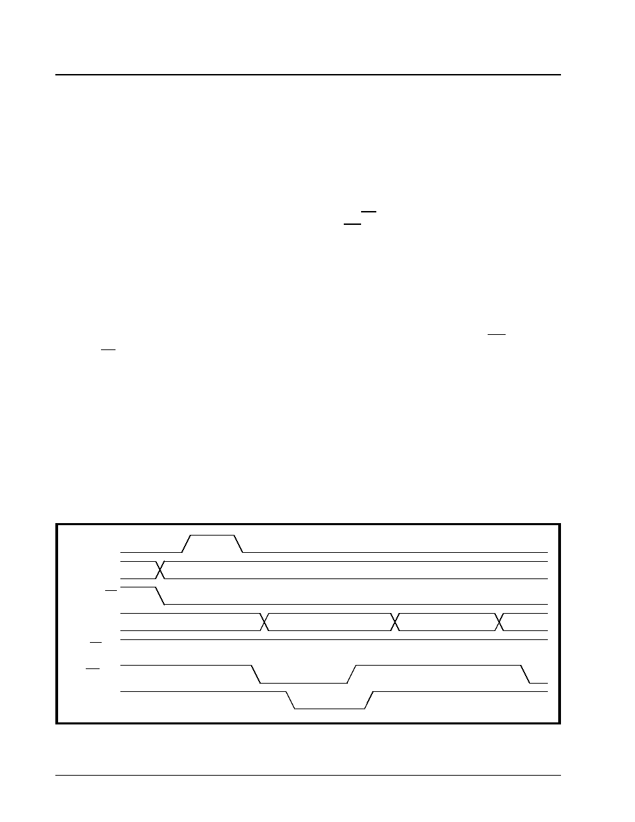
XRT7250
DS3/E3 FRAMER IC
·Á
·Á
·Á
·Á
REV. 1.1.1
46
a. Perform the initial write operation of the burst
access.
b. Perform the remaining write operations, of the
burst access.
c. Terminate the burst access operation.
Each of these operations within the burst access are
described below.
2.2.2.2.1.2.1
The Initial Write Operation
The initial write operation of an Intel-type Write Burst
Access is accomplished by executing a Programmed
I/O write cycle as summarized below.
A.0
Execute a Single Ordinary (Programmed I/
O) Write cycle, as described in Steps A.1
through A.7 below.
A.1
Place the address of the initial target register
(or buffer location) within the Framer, on the
Address Bus pins, A[8:0].
A.2
At the same time, the Address-Decoding cir-
cuitry (within the user's system) should assert
the CS (Chip Select) input pin of the Framer, by
toggling it "Low". This step enables further
communication between the µC/µP and the
Framer Microprocessor Interface block.
A.3
Assert the ALE_AS (Address Latch Enable)
input pin "High". This step enables the Address
Bus input drivers, within the Microprocessor
Interface Block of the Framer.
A.4
After allowing the data on the Address Bus pins
to settle (by waiting the appropriate Address
Setup time), the µC/µP should then toggle the
ALE_AS input pin "Low". This step latches the
contents, on the Address Bus pins, A[8:0], into
the XRT7250 DS3/E3 Framer Microprocessor
Interface block. At this point, the initial address
of the burst access has now been selected.
N
OTE
: The ALE_AS input pin should remain "Low" for the
remainder of this Burst I/O Access operation.
A.5
Next, the µC/µP should indicate that this cur-
rent bus cycle is a Write operation by keeping
the RD_DS pin "High" and toggling the
WR_RW (Write Strobe) pin "Low". This action
also enables the bi-directional data bus input
drivers of the Framer device.
A.6
The µC/µP places the byte (or word) that it
intends to write into the target register on the
bi-directional data bus, D[7:0].
A.7
After waiting the appropriate amount of time, for
the data (on the bi-directional data bus) to set-
tle, the µC/µP should toggle the WR_RW (Write
Strobe) input pin "High". This action accom-
plishes two things.
a. It latches the contents of the bi-directional data
bus into the XRT7250 DS3/E3 Framer Micropro-
cessor Interface Block.
b. It terminates the write cycle.
Figure 31 presents a timing diagram which illustrates
the behavior of the Microprocessor Interface signals,
during the initial write operation within a Burst Ac-
cess, for an Intel-type µC/µP.
At the completion of this initial write cycle, the µC/µP
has written a byte or word into the first register or
buffer location (within the XRT7250 DS3/E3 Framer)
for this particular burst access operation. In order to
F
IGURE
31. B
EHAVIOR
OF
THE
M
ICROPROCESSOR
I
NTERFACE
SIGNALS
,
DURING
THE
I
NITIAL
W
RITE
O
PERATION
OF
A
B
URST
C
YCLE
(I
NTEL
-
TYPE
P
ROCESSOR
)
Address of Initial Target Register (offset = 0x00)
Data to be written (offset = 0x00)
ALE_AS
A[8:0]
CS
D[7:0]
RD_DS
WR_RW
RDY_DTCK
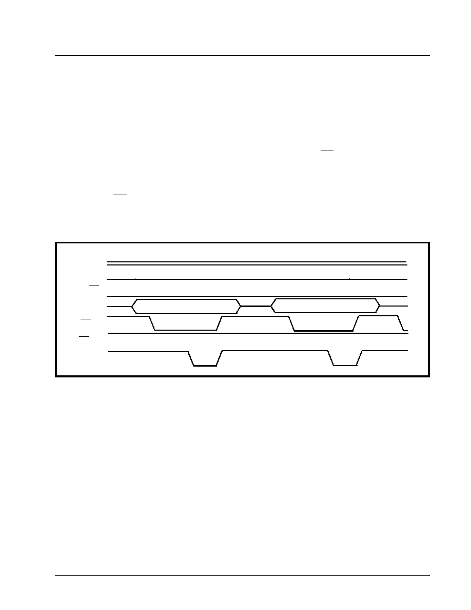
·Á
·Á
·Á
·Á
DS3/E3 FRAMER IC
XRT7250
REV. 1.1.1
47
illustrate this point, the byte (or word) of data, that is
being written in Figure 31 has been labeled Data to
be Written (Offset = 0x00).
2.2.2.2.1.2.2
The Subsequent Write Operations
The procedure that the µC/µP must use to perform
the remaining write cycles, within this burst access
operation, is presented below.
B.0
Execute each subsequent write cycle, as
described in steps B.1 through B.3.
B.1
Without toggling the ALE_AS input pin (e.g.,
keeping it "Low"), apply the value of the next
byte or word (to be written into the Framer) to
the bi-directional data bus pins, D[7:0].
B.2
Toggle the WR_RW (Write Strobe) input pin
"Low". This step accomplishes two things.
a. It enables the input drivers of the bi-directional
data bus.
b. It causes the Framer to internally increment the
value of the latched address.
B.3
After waiting the appropriate amount of settling
time the data, in the internal data bus, will stabi-
lize and is ready to be latched into the Framer
Microprocessor Interface block. At this point,
the µC/µP should latch the data into the Framer
by toggling the WR_RW input pin "High".
For subsequent write operations, within this burst I/O
access, the µC/µP simply repeats steps B.1 through
B.3, as illustrated in Figure 32.
2.2.2.2.1.2.3
Terminating the Burst I/O Access
Burst Access Operation will be terminated upon the
rising edge of the ALE_AS input signal. At this point
the Framer will cease to internally increment the
latched address value. Further, the µC/µP is now free
to execute either a Programmed I/O access or to start
another Burst Access Operation with the XRT7250
DS3/E3 Framer.
2.2.2.2.2
Burst I/O Access in the Motorola
Mode
If the XRT7250 DS3/E3 Framer is interfaced to a Mo-
torola-type µC/µP (e.g., the MC680x0 family, etc.),
then it should be configured to operate in the Motoro-
la mode (by tying the MOTO pin to VCC). Motorola-
type Read and Write Burst I/O Access operations are
described below.
2.2.2.2.2.1
The Motorola-Mode Read Burst I/O
Access Operation
Whenever a Motorola-type µC/µP wishes to read the
contents of numerous registers or buffer locations
over a contiguous range of addresses, then it should
do the following.
a. Perform the initial Read operation of the burst
access.
b. Perform the remaining read operations in the
burst access.
c. Terminate the burst access operation.
Each of these operations, within the Burst Access are
discussed below.
2.2.2.2.2.1.1
The Initial Read Operation
The initial read operation of a Motorola-type read
burst access is accomplished by executing a Pro-
grammed I/O Read cycle, as summarized below.
A.0
Execute a Single Ordinary (Programmed I/
O) Read Cycle, as described in steps A.1
through A.8 below.
F
IGURE
32. B
EHAVIOR
OF
THE
M
ICROPROCESSOR
I
NTERFACE
S
IGNALS
,
DURING
SUBSEQUENT
W
RITE
O
PERATIONS
WITHIN
THE
B
URST
I/O C
YCLE
ALE_AS
WR_RW
A[8:0]
CS
D[15:0]
RDY_DTCK
Data Written at Offset =0x01
RD_DS
Data Written at Offset =0x02
Address of "Initial" Target Register (Offset = 0x00)
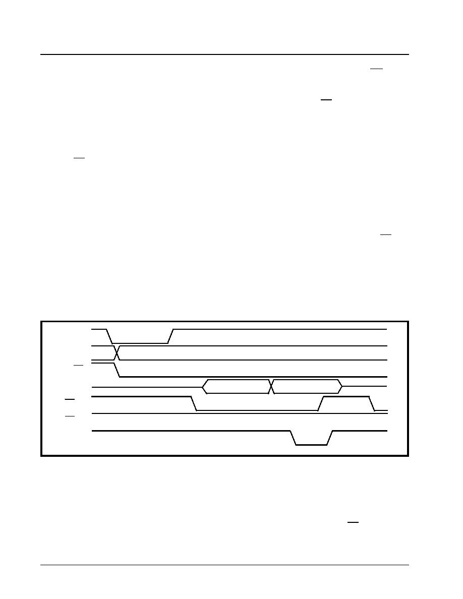
XRT7250
DS3/E3 FRAMER IC
·Á
·Á
·Á
·Á
REV. 1.1.1
48
A.1
Assert the ALE_AS (AS*) input pin by toggling
it "Low". This step enables the Address Bus
input drivers (within the XRT7250 DS3/E3
Framer) within the Framer Microprocessor
Interface Block.
A.2
Place the address of the initial target register or
buffer location (within the Framer), on the
Address Bus input pins, A[8:0].
A.3
At the same time, the Address-Decoding cir-
cuitry (within the user's system) should assert
the CS (Chip Select) input pins of the Framer
by toggling it "Low". This action enables further
communication between the µC/µP and the
Framer Microprocessor Interface block.
A.4
After allowing the data on the Address Bus pins
to settle (by waiting the appropriate Address
Setup time), the µC/µP should toggle the
ALE_AS input pin "High". This step causes the
Framer device to latch the contents of the
Address Bus into its internal circuitry. At this
point, the initial address of the burst access has
now been selected.
A.5
Further, the µC/µP should indicate that this
cycle is a Read cycle by setting the WR_RW
(R/W*) input pin "High".
A.6
Next the µC/µP should initiate the current bus
cycle by toggling the RD_DS (Data Strobe)
input pin "Low". This step will enable the bi-
directional data bus output drivers, within the
XRT7250 DS3/E3 Framer device. At this point,
the bi-directional data bus output drivers will
proceed to driver the contents of the Address
register onto the bi-directional data bus.
A.7
After some settling time, the data on the bi-
directional data bus will stabilize and can be
read by the µC/µP. The XRT7250 DS3/E3
Framer will indicate that this data can be read
by asserting the RDY_DTCK (DTACK) signal.
A.8
After the µC/µP detects the RDY_DTCK signal
(from the XRT7250 DS3/E3 Framer) it will ter-
minate the Read Cycle by toggling the RD_DS
(Data Strobe) input pin "High".
Figure 33 presents an illustration of the behavior of
the Microprocessor Interface Signals during the initial
Read Operation, within a Burst I/O Cycle, for a Motor-
ola-type µC/µP.
At the completion of this initial read cycle, the µC/µP
has read in the contents of the first register or buffer
location (within the XRT7250 DS3/E3 Framer) for this
particular burst access operation. In order to illus-
trate how this burst I/O cycle works, the byte (or word)
of data, that is being read in Figure 33 has been la-
beled Valid Data at Offset = 0x00. This indicates that
the µC/µP is reading the very first register (or buffer
location) in this burst access.
2.2.2.2.2.1.2
The Subsequent Read Operations
The procedure that the µC/µP must use to perform
the remaining read cycles, within this Burst Access
operation, is presented below.
B.0
Execute each subsequent Read Cycle, as
described in steps B.1 through B.3, below.
B.1
Without toggling the ALE_AS input pin (e.g.,
keeping it "High"), toggle the RD_DS (Data
Strobe) input pin "Low". This step accom-
plishes the following.
F
IGURE
33. B
EHAVIOR
OF
THE
M
ICROPROCESSOR
I
NTERFACE
S
IGNALS
,
DURING
THE
I
NITIAL
R
EAD
O
PERATION
OF
A
B
URST
C
YCLE
(M
OTOROLA
T
YPE
P
ROCESSOR
)
ALE_AS
RD_DS
A[8:0]
CS
D[15:0]
Rdy_Dtck
Not Valid
Valid Data at Offset = 0x00
Address of "Initial" Target Register (Offset = 0x00)
WR_RW
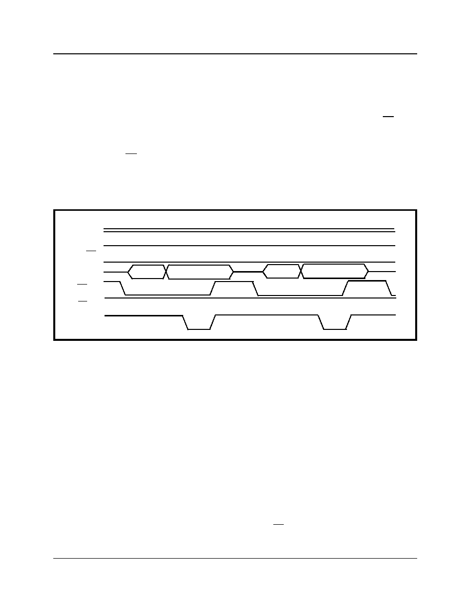
·Á
·Á
·Á
·Á
DS3/E3 FRAMER IC
XRT7250
REV. 1.1.1
49
a. The Framer internally increments the latched
address value (within the Microprocessor Inter-
face circuitry).
b. The output drivers of the bi-directional data bus
(D[7:0]) are enabled. At some time later, the reg-
ister or buffer location corresponding to the incre-
mented latched address value will be driven onto
the bi-directional data bus.
N
OTE
: In order to insure that the XRT7250 DS3/E3 Framer
device will interpret this signal as being a Read signal, the
µC/µP
should keep the WR_RW input pin "High".
B.2
After some settling time, the data on the bi-
directional data bus will stabilize and can be
read by the µC/µP. The XRT7250 DS3/E3
Framer will indicate that this data is ready to be
read by asserting the RDY_DTCK (DTACK*)
signal.
B.3
After the µC/µP detects the RDY_DTCK signal
(from the XRT7250 DS3/E3 Framer), it termi-
nates the Read cycle by toggling the RD_DS
(Data Strobe) input pin "High".
For subsequent read operations, within this burst cy-
cle, the µC/µP simply repeats steps B.1 through B.3,
as illustrated in Figure 34.
2.2.2.2.2.1.3
Terminating the Burst Access
Operation
The Burst I/O Access will be terminated upon the fall-
ing edge of the ALE_AS input signal. At this point the
Framer will cease to internally increment the latched
address value. Further, the µC/µP is now free to exe-
cute either a Programmed I/O access or to start an-
other Burst Access Operation with the XRT7250 DS3/
E3 Framer.
2.2.2.2.2.2
The Motorola-Mode Write Burst
Access
Whenever a Motorola-type µC/µP wishes to write the
contents of numerous registers or buffer locations
over a contiguous range of addresses, then it should
do the following.
a. Perform the initial write operation of the burst
access.
b. Perform the remaining write operations, of the
burst access.
c. Terminate the burst access operation.
Each of these operations within the burst access are
described below.
2.2.2.2.2.2.1
The Initial Write Operation
The initial write operation of a Motorola-type Write
Burst Access is accomplished by executing a Pro-
grammed I/O Write Cycle as summarized below.
A.0
Execute a Single Ordinary (Programmed I/
O) Write cycle, as described in Steps A.1
through A.7 below.
A.1
Assert the ALE_AS (Address Strobe) input pin
by toggling it "Low". This step enables the
Address Bus input drivers (within the XRT7250
DS3/E3 Framer).
A.2
Place the address of the initial target register or
buffer location (within the Framer), on the
Address Bus input pins, A[8:0].
A.3
At the same time, the Address-Decoding cir-
cuitry (within the user's system) should assert
the CS input pin of the Framer by toggling it
"Low". This step enables further communica-
F
IGURE
34. B
EHAVIOR
THE
M
ICROPROCESSOR
I
NTERFACE
S
IGNALS
,
DURING
SUBSEQUENT
R
EAD
O
PERATIONS
WITHIN
THE
B
URST
I/O C
YCLE
(M
OTOROLA
-
TYPE
µC/µP)
ALE_AS
RD_DS
A[8:0]
CS
D[15:0]
RDY_DTCK
Not Valid
Valid Data at Offset
WR_RW
Not Valid
Valid Data at Offset
Address of "Initial" Target Register (Offset =
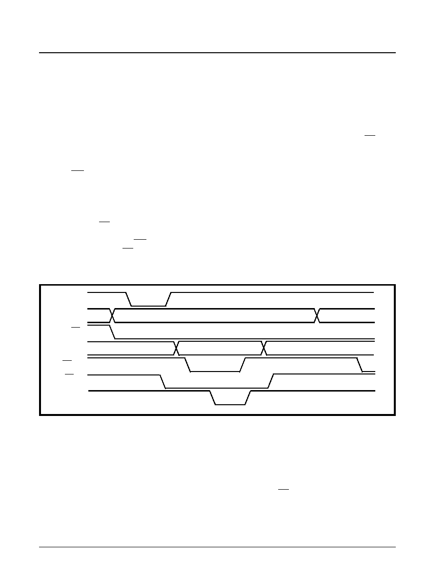
XRT7250
DS3/E3 FRAMER IC
·Á
·Á
·Á
·Á
REV. 1.1.1
50
tion between the µC/µP and the Framer Micro-
processor Interface block.
A.4
After allowing the data on the Address Bus pins
to settle (by waiting the appropriate Address
Setup time), the µC/µP should toggle the
ALE_AS input pin "High". This step causes the
Framer device to latch the contents of the
Address Bus into its own circuitry. At this point,
the initial address of the burst access has now
been selected.
A.5
Further, the µC/µP should indicate that this cur-
rent bus cycle is a Write operation by toggling
the WR_RW (R/W*) input pin "Low".
A.6
The µC/µP should then place the byte or word
that it intends to write into the target register, on
the bi-directional data bus, D[7:0].
A.7
Next, the µC/µP should initiate the bus cycle by
toggling the RD_DS (Data Strobe) input pin
"Low". When the XRT7250 DS3/E3 Framer
device senses that the WR_RW input pin is
"Low", and that the RD_DS input pin has tog-
gled "Low" it will enable the input drivers of the
bi-directional data bus, D[7:0].
A.8
After waiting the appropriate amount of time, for
this newly placed data to settle on the bi-direc-
tional data bus (e.g., the Data Setup time) the
Framer will assert the RDY_DTCK (DTACK)
output signal.
A.9
After the µP/µC detects the RDY_DTCK signal
(from the Framer) it should toggle the RD_DS
input pin "High". This action accomplishes two
things:
a. It latches the contents of the bi-directional data
bus into the XRT7250 DS3/E3 Framer Micropro-
cessor Interface block.
b. It terminates the Write cycle.
Figure 35 presents a timing diagram which illustrates
the behavior of the Microprocessor Interface signals,
during the Initial write operation within a Burst Ac-
cess, for a Motorola-type µC/µP.
At the completion of this initial write cycle, the µC/µP
has written a byte or word into the first register or
buffer location (within the XRT7250 DS3/E3 Framer)
for this particular burst I/O access. In order to illus-
trate how this burst I/O cycle works, the byte (or word)
of data, that is being written in Figure 35 has been la-
beled Data to be Written (Offset = 0x00).
2.2.2.2.2.2.2
The Subsequent Write Operations
The procedure that the µC/µP must use to perform
the remaining write cycles, within this burst access
operation, is presented below.
B.0
Execute each subsequent write cycle, as
described in Steps B.1 through B.3
B.1
Without toggling the ALE_AS (Address Strobe)
input pin (e.g., keeping it "High"), apply the
value of the next byte or word (to be written into
the Framer) to the bi-directional data bus pins,
D[7:0].
B.2
Toggle the RD_DS (Data Strobe) input pin
"Low". This step accomplishes the following.
a. The Framer internally increments the latched
address value (within the Microprocessor Inter-
face).
F
IGURE
35. B
EHAVIOR
OF
THE
M
ICROPROCESSOR
I
NTERFACE
SIGNALS
,
DURING
THE
I
NITIAL
W
RITE
O
PERATION
OF
A
B
URST
C
YCLE
(M
OTOROLA
-
TYPE
P
ROCESSOR
)
ALE_AS
A[8:0]
CS
D[15:0]
RD_DS
RDY_DTCK
Data to be Written (Offset = 0x00)
Address of "Initial" Target Register (Offset = 0x00)
WR_RW
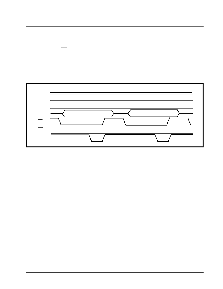
·Á
·Á
·Á
·Á
DS3/E3 FRAMER IC
XRT7250
REV. 1.1.1
51
b. The input drivers of the bi-directional data bus are
enabled.
N
OTE
: In order to insure that the XRT7250 DS3/E3 Framer
device will interpret this signal as being a Write signal, the
µC/µP
should keep the WR_RW input pin "Low".
B.3
After some settling time, the data, in the inter-
nal data bus, will stabilize and is ready to be
latched into the Framer Microprocessor Inter-
face block. The Microprocessor Interface block
will indicate that this data is ready to be latched
by asserting the RDY_DTCK (DTACK) output
signal. At this point, the µC/µP should latch the
data into the Framer by toggling the RD_DS
input pin "High".
For subsequent write operations, within this burst I/O
access, the µC/µP simply repeats steps B.1 through
B.3 as illustrated in Figure 36.
2.2.2.2.2.2.3
Terminating the Burst I/O Access
The Burst I/O Access will be terminated upon the fall-
ing edge of the ALE_AS input signal. At this point the
Framer will cease to internally increment the latched
address value. Further, the µC/µP is now free to exe-
cute either a Programmed I/O access or to start an-
other Burst I/O Access with the XRT7250 DS3/E3
Framer.
2.3
O
N
-C
HIP
R
EGISTER
O
RGANIZATION
The Microprocessor Interface section, within the
Framer device allows the user to do the following.
∑ Configure the Framer into a wide variety of operat-
ing modes.
∑ Employ various features of the Framer device.
∑ Perform status monitoring
∑ Enable/Disable and service Interrupt Conditions
All of these things are accomplished by reading from
and writing to the many on-chip registers within the
Framer device. Table 4 lists each of these registers
and their corresponding address locations within the
Framer Address space.
2.3.1
Framer Register Addressing
The array of on-chip registers consists of a variety of
register types. These registers are denoted in
Table 4, as follows.
R/O - Read Only Registers.
R/W - Read/Write Registers
RUR - Reset-upon-Read Registers
Additionally, some of these registers consists of both
R/O and R/W bit-fields. These registers are denoted
in Table 4 as Combination of R/W and R/O.
The bit-format and definitions for each of these regis-
ters are presented in Section 3.3.2
F
IGURE
36. B
EHAVIOR
OF
THE
M
ICROPROCESSOR
I
NTERFACE
S
IGNALS
,
DURING
SUBSEQUENT
W
RITE
O
PERATIONS
WITH
THE
B
URST
I/O C
YCLE
(M
OTOROLA
-
TYPE
µC/µP)
ALE_AS
RD_DS
A[8:0]
CS
D[15:0]
RDY_DTCK
Data Written at Offset =0x01
WR_RW
Data Written at Offset =0x02
Address of "Initial" Target Register (Offset = 0x00)

XRT7250
DS3/E3 FRAMER IC
·Á
·Á
·Á
·Á
REV. 1.1.1
52
T
ABLE
4: R
EGISTER
A
DDRESSING
OF
THE
F
RAMER
P
ROGRAMMER
R
EGISTERS
A
DDRESS
R
EGISTER
N
AME
P
OWER
U
P
D
EFAULT
V
ALUE
R
EGISTER
TYPE
0x00
Operating Mode register
b00100011
R/W
0x01
I/O Control Register
b10100000
R/W, R/O
0x02
Part Number Register
b00000001
R/O
0x03
Version Number Register
b00000011
R/O
0x04
Block Interrupt Enable Register
b00000000
R/W
0x05
Block Interrupt Status Register
b00000000
R/O
0x06
Reserved
0x07
Reserved
0x08
Reserved
0x09
Reserved
0x0A
Reserved
0x0B
Reserved
0x0C
Reserved
0x0D
Reserved
0x0E
Reserved
0x0F
Reserved
0x10
RxDS3 Configuration & Status Register
RxE3 Configuration & Status Register 1 - G.832
RxE3 Configuration & Status Register 1 - G.751
b00010000
b00000010
b00000010
R/W, R/O
0x11
RxDS3 Status Register
RxE3 Configuration & Status Register 2 - G.832
RxE3 Configuration & Status Register 2 - G.751
b00000000
b01100111
b01100111
R/W, R/O
0x12
RxDS3 Interrupt Enable Register
RxE3 Interrupt Enable Registers -1 G.832
RxE3 Interrupt Enable Registers - 1 G.751
b00000000
b00000000
b00000000
R/W, R/O
0x13
RxDS3 Interrupt Status Register
RxE3 Interrupt Enable Register -2 G.832
RxE3 Interrupt Enable Register - 2 G.751
b00000000
b00000000
b00000000
R/W, R/O
0x14
RxDS3 Sync Detect Enable Register
RxE3 Interrupt Status Register 1 - G.832
RxE3 Interrupt Status Register 1 - G.751
b00011111
b00000000
b00000000
RUR, R/O
0x15
RxE3 Interrupt Status Register 2 - G.832
RxE3 Interrupt Status Register 2 - G.751
b00000000
b00000000
RUR, R/O
0x16
RxDS3 FEAC Register
b01111110
R/O
0x17
RxDS3 FEAC Interrupt Enable/Status Register
b00000000
R/O
0x18
RxDS3 LAPD Control Register
RxE3 LAPD Control Register
b00000000
R/W, RUR

·Á
·Á
·Á
·Á
DS3/E3 FRAMER IC
XRT7250
REV. 1.1.1
53
0x19
RxDS3 LAPD Status Register
RxE3 LAPD Status Register
b00000000
b00000000
R/O
0x1A
RxE3 NR Byte Register - G.832
RxE3 Service Bit Register G.751
b00000000
b00000000
R/O
0x1B
RxE3 GC Byte Register - G.832
b00000000
R/O
0x1C
RxE3 TTB-0 Register - G.832
b00000000
R/O
0x1D
RxE3 TTB-1 Register - G.832
b00000000
R/O
0x1E
RxE3 TTB-2 Register - G.832
b00000000
R/O
0x1F
RxE3 TTB-3 Register - G.832
b00000000
R/O
0x20
RxE3 TTB-4 Register - G.832
b00000000
R/O
0x21
RxE3 TTB-5 Register - G.832
b00000000
R/O
0x22
RxE3 TTB-6 Register - G.832
b00000000
R/O
0x23
RxE3 TTB-7 Register - G.832
b00000000
R/O
0x24
RxE3 TTB-8 Register - G.832
b00000000
R/O
0x25
RxE3 TTB-9 Register - G.832
b00000000
R/O
0x26
RxE3 TTB-10 Register - G.832
b00000000
R/O
0x27
RxE3 TTB-11 Register - G.832
b00000000
R/O
0x28
RxE3 TTB-12 Register - G.832
b00000000
R/O
0x29
RxE3 TTB-13 Register - G.832
b00000000
R/O
0x2A
RxE3 TTB-14 Register - G.832
b00000000
R/O
0x2B
RxE3 TTB-15 Register - G.832
b00000000
R/O
0x2C - 0x2F Reserved
b00000000
R/O
0x30
TxDS3 Configuration Register
TxE3 Configuration Register - G.832
TxE3 Configuration Register - G.751
b00000111
b00000000
b00000000
R/W
0x31
TxDS3 FEAC Configuration and Status Register
b00000000
R/O, R/W, RUR
0x32
TxDS3 FEAC Register
b01111110
R/W
0x33
TxDS3 LAPD Configuration Register
TxE3 LAPD Configuration Register
b00000000
b00000000
R/W
0x34
TxDS3 LAPD Status/Interrupt Register
TxE3 LAPD Status/Interrupt Register
b00000000
b00000000
R/W, R/O, RUR
0x35
TxDS3 M-Bit Mask Register
TxE3 GC Byte Register - G.832
TxE3 Service Bits Register - G.751
b00000000
b00000000
b00000000
R/W
0x36
TxDS3 F-Bit Mask Register 1
TxE3 MA Byte Register - G.832
b00000000
b00000000
R/W
T
ABLE
4: R
EGISTER
A
DDRESSING
OF
THE
F
RAMER
P
ROGRAMMER
R
EGISTERS
A
DDRESS
R
EGISTER
N
AME
P
OWER
U
P
D
EFAULT
V
ALUE
R
EGISTER
TYPE

XRT7250
DS3/E3 FRAMER IC
·Á
·Á
·Á
·Á
REV. 1.1.1
54
0x37
TxDS3 F-Bit Mask Register 2
TxE3 NR Byte Register - G.832
b00000000
b00000000
R/W
0x38
TxDS3 F-Bit Mask Register 3
TxE3 TTB-0 Register - G.832
b00000000
b00000000
R/W
0x39
TxDS3 F-Bit Mask Register 4
TxE3 TTB-1 Register - G.832
b00000000
b00000000
R/W
0x3A
TxE3 TTB-2 Register - G.832
b00000000
R/W
0x3B
TxE3 TTB-3 Register - G.832
b00000000
R/W
0x3C
TxE3 TTB-4 Register - G.832
b00000000
R/W
0x3D
TxE3 TTB-5 Register - G.832
b00000000
R/W
0x3E
TxE3 TTB-6 Register - G.832
b00000000
R/W
0x3F
TxE3 TTB-7 Register - G.832
b00000000
R/W
0x40
TxE3 TTB-8 Register - G.832
b00000000
R/W
0x41
TxE3 TTB-9 Register - G.832
b00000000
R/W
0x42
TxE3 TTB-10 Register - G.832
b00000000
R/W
0x43
TxE3 TTB-11 Register - G.832
b00000000
R/W
0x44
TxE3 TTB-12 Register - G.832
b00000000
R/W
0x45
TxE3 TTB-13 Register - G.832
b00000000
R/W
0x46
TxE3 TTB-14 Register - G.832
b00000000
R/W
0x47
TxE3 TTB-15 Register - G.832
b00000000
R/W
0x48
TxE3 FA1 Error Mask Register - G.832
TxE3 FAS Error Mask Upper Register - G.751
b00000000
b00000000
R/W
0x49
TxE3 FA2 Error Mask Register - G.832
TxE3 FAS Error Mask Lower Register - G.751
b00000000
b00000000
R/W
0x4A
TxE3 BIP-8 Mask Register - G.832
TxE3 BIP-4 Mask Register - G.751
b00000000
b00000000
R/W
0x4B - 0x4F Reserved
0x50
PMON LCV Event Count Register - MSB
b00000000
RUR
0x51
PMON LCV Event Count Register - LSB
b00000000
RUR
0x52
PMON Framing Bit Error Event Count Register - MSB
b00000000
RUR
0x53
PMON Framing Bit Error Event Count Register - LSB
b00000000
RUR
0x54
PMON Parity Error Event Count Register - MSB
b00000000
RUR
0x55
PMON Parity Error Event Count Register - LSB
b00000000
RUR
0x56
PMON FEBE Event Count Register - MSB
b00000000
RUR
0x57
PMON FEBE Event Count Register - LSB
b00000000
RUR
T
ABLE
4: R
EGISTER
A
DDRESSING
OF
THE
F
RAMER
P
ROGRAMMER
R
EGISTERS
A
DDRESS
R
EGISTER
N
AME
P
OWER
U
P
D
EFAULT
V
ALUE
R
EGISTER
TYPE

·Á
·Á
·Á
·Á
DS3/E3 FRAMER IC
XRT7250
REV. 1.1.1
55
2.3.2
Framer Register Description
This section provides a function description of each
bit-field within each of the on-chip Framer Registers.
N
OTE
: For all on-chip registers, a table containing the bit-
format of the register is presented. Additionally, these
tables also contain the default values for each of these reg-
ister bits. Finally, the functional description, associated with
each register bit-field is presented, along with a reference to
a Section Number, within this Data Sheet, that provides a
more in-depth discussion of the functions associated with
this register bit-field.
2.3.2.1
Framer Operating Mode Register
Bit 7 - Local Loopback Mode
0x58
PMON CP Bit Error Event Count Register - MSB
b00000000
RUR
0x59
PMON CP Bit Error Event Count Register - LSB
b00000000
RUR
0x5A - 0x6B Reserved
b00000000
RUR
0x6C
PMON Holding Register
b00000000
RUR
0x6D
One-Second Error Status Register
b00000000
R/O
0x6E
LCV One-Second Accumulator Register - MSB
b00000000
R/O
0x6F
LCV One-Second Accumulator Register - LSB
b00000000
R/O
0x70
Frame Parity Error One-Second Accumulator Register -
MSB (BIP-8 in G.832)
b00000000
R/O
0x71
Frame Parity Error One-Second Accumulator Register -
LSB (BIP-8 in G.832)
b00000000
R/O
0x72
Frame CP Bit Error - One-Second Accumulator Register -
MSB
b00000000
R/O
0x73
Frame CP Bit Error - One-Second Accumulator Register -
LSB
b00000000
R/O
0x72 - 0x7F Reserved
0x80
Line Interface Drive Register
b00001000
R/W
0x81
Line Interface Scan Register
b00000000
R/O
0x82 - 0x85 Reserved
0x86 - 0xDD Transmit LAPD Message Buffer (RAM)
bxxxxxxx
R/W
0xDE -
0x135
Receive LAPD Message Buffer (RAM)
bxxxxxxx
R/W
T
ABLE
4: R
EGISTER
A
DDRESSING
OF
THE
F
RAMER
P
ROGRAMMER
R
EGISTERS
A
DDRESS
R
EGISTER
N
AME
P
OWER
U
P
D
EFAULT
V
ALUE
R
EGISTER
TYPE
FRAMER OPERATING MODE REGISTER (ADDRESS = 0X00)
B
IT
7
B
IT
6
B
IT
5
B
IT
4
B
IT
3
B
IT
2
B
IT
1
B
IT
0
Local Loopback
DS3/E3*
Internal
LOS
Enable
RESET
Interrupt
Enable Reset
Frame Format
TimRefSel[1:0]
R/W
R/W
R/W
R/W
R/W
R/W
R/W
R/W
0
0
1
0
1
0
1
1

XRT7250
DS3/E3 FRAMER IC
·Á
·Á
·Á
·Á
REV. 1.1.1
56
This Read/Write bit-field permits the user to com-
mand the Framer chip to operate in the Local Loop-
back Mode.
Setting this bit-field to "0", configures the Framer chip
to operate in the Normal Mode. Setting this bit-field
to "1", configures the Framer chip to operate in the
Local-Loopback Mode.
N
OTE
: For a detailed description of the Local Loopback
Mode, please see Section 6.0
Bit 6 - DS3/E3* Select
This Read/Write bit-field permits the user to com-
mand the Framer chip to operate in either the DS3
Mode or the E3 Mode.
Setting this bit-field to "0", configures the Framer chip
to operate in the E3 Mode. Setting this bit-field to "1",
configures the Framer chip to operate in the DS3
Mode.
Bit 5 - Internal LOS Enable Select
This Read/Write bit-field permits the user to configure
the Framer chip to either declare an LOS condition,
based upon the Internal Circuit's criteria or not.
Setting this bit-field to "0", configures the Framer chip
to NOT declare an LOS condition, based upon its
own internal criteria.
Setting this bit-field to "1", configures the Framer chip
to declare an LOS condition based upon its own inter-
nal criteria.
N
OTES
:
1. The XRT7250 Framer Chip will declare an LOS
condition, anytime the RLOS input pin (pin 78) is
set "High", independent of the setting of this bit-
field.
2. For more information on the XRT7250 Framer
device's internal criteria for Loss of Signal please
see Section 3.3.2.5.
Bit 4 - RESET:
This Read/Write bit-field permits the user to com-
mand the XRT7250 Framer chip into the Reset state.
If the XRT7250 Framer chip is commanded into the
Reset state, all of its internal register bits will auto-
matically be set to their default condition.
Setting this bit-field to "0" configures the XRT7250
Framer chip to operate normally. Setting this bit-field
to "1" configures the XRT7250 Framer chip to go into
the Reset Mode.
Bit 3 - Interrupt Enable Reset
This Read/Write bit-field permits the user to configure
the XRT7250 Framer chip to automatically disable all
Interrupts that are activated.
Setting this bit-field to "0" configures the XRT7250
Framer chip to NOT disable the Interrupt Enable Sta-
tus, of any interrupts, following their activation.
Setting this bit to "1" configures the XRT7250 Framer
chip to automatically disable any interrupt that is acti-
vated.
N
OTE
: For more information on this feature, please see
Section 1.6.1.
Bit 2 - Frame Format Select
This Read/Write bit-field, along with the DS3/E3 se-
lect bit-field (bit 6 in this register) permits the user to
select the Framing Format that the XRT7250 will op-
erate in. The following table relates the states of this
bit-field (bit 2) and that of bit 6 to the selected framing
format for this chip.
Bits 1 & 0 - TimRefSel[1:0] - Timing Reference Se-
lect
These two Read/Write bit-fields permits the user to
select both a Framing Reference and Timing Refer-
ence for the Transmit Section of the XRT7250. The
following table relates the states of these two bit-
fields to the selected Framing and Timing references.
N
OTE
: For more information on Framing and Timing Refer-
ences, please see Section 3.2.
B
IT
6 - DS3/E3*
S
ELECT
B
IT
2 - F
RAME
F
ORMAT
S
ELECT
S
ELECTED
F
RAMING
F
ORMAT
0
0
E3, ITU-T G.751
0
1
E3, ITU-T G.832
1
0
DS3, C-bit Parity
1
1
DS3, M13
T
IM
R
EF
S
EL
[1:0]
F
RAMING
R
EFERENCE
T
IMING
R
EFERENCE
00
Asynchronous
RxLineClk Input
Signal
01
TxFrameRef
TxInClk Input sig-
nal
10
Asynchronous
TxInClk Input sig-
nal
11
Asynchronous
TxInClk Input sig-
nal

·Á
·Á
·Á
·Á
DS3/E3 FRAMER IC
XRT7250
REV. 1.1.1
57
2.3.2.2
I/O Control Register
Bit 7 - DisableTxLOC
This Read/Write bit-field permits the user to enable or
disable the Transmit Loss of Clock feature.
Setting this bit-field to "0" enables the Transmit Loss
of Clock feature. Conversely, setting this bit-field to
"1" disables the Transmit Loss of Clock feature.
N
OTE
: For more details into the Transmit Loss of Clock fea-
ture, please see Section 1.4.
Bit 6 - LOC (Loss of Clock) Status
This Read-Only bit-field reflects the Loss of Clock
status for the XRT7250. The XRT7250 will set this
bit-field to "0" under normal operation conditions.
Conversely, if the XRT7250 has experiences a Loss
of Clock event, then it will set this bit-field to "1".
N
OTE
: For more details into the Loss of Clock status,
please see Section 1.4.
Bit 5 - DisableRxLOC
This Read/Write bit-field permits the user to enable or
disable the Receive Loss of Clock feature.
Setting this bit-field to "0" enables the Receive Loss
of Clock feature. Conversely, setting this bit-field to
"1" disables the Receive Loss of Clock feature.
N
OTE
: For more details into the Receive Loss of Clock fea-
ture, please see Section 1.4.
Bit 4 - AMI/ZeroSup*
This Read/Write bit-field permits the user to configure
the XRT7250 to transmit and receive data via the AMI
(Alternate Mark Inversion) line code or via a Zero-
Suppression (e.g, B3ZS/HDB3) line code.
Setting this bit-field to "0" configures the XRT7250 to
transmit and receive data via a Zero-Suppression line
code.
Setting this bit-field to "1" configures the XRT7250 to
transmit and receive data via the Alternate Mark In-
version line code.
N
OTES
:
1. If the XRT7250 is configured to transmit and
receive data, using a Zero-Suppression code, while
operating in the DS3 Mode, then the chip will trans-
mit and receive data using the B3ZS Line Code.
2. If the XRT7250 is configured to transmit and
receive data, using a Zero-Suppression code, while
operating in the E3 Mode, then the chip will trans-
mit and receive data using the HDB3 Line Code.
3. This bit-field will be ignored if bit 3 (Unipolar/Bipo-
lar*) of this Register is set to "1" (for Unipolar
Mode).
Bit 3 - Unipolar/Bipolar*
This Read/Write bit-field permits the user to configure
the XRT7250 to transmit data to and receive data
from an LIU IC, in either the Single-Rail or Dual-Rail
format.
Setting this bit-field to "0" configures the XRT7250 to
operate in the Bipolar or Dual-Rail Format. In this
mode, the Transmit Section of the XRT7250 will out-
put data to the LIU via both the TxPOS and TxNEG
output pins. Additionally, the Receive Section of the
device will receive data from the LIU via both the Rx-
POS and RxNEG output pins.
Setting this bit-field to "1" configures the XRT7250 to
operate in the Unipolar or Single-Rail Format. In this
mode, the Transmit Section of the XRT7250 will out-
put data to the LIU, in a binary data stream manner
via the TxPOS output pin. Additionally, the Receive
Section of the device will receive data from the LIU, in
a binary data stream manner, via the RxPOS input
pin.
N
OTE
: For more information on the transmission and
reception of data in the Single-Rail or Dual-Rail format,
please see Section 3.2.5.
Bit 2 - TxLineClk Invert
This Read/Write bit-field permits the user to configure
the XRT7250 to output data, via the TxPOS and Tx-
NEG output pins, on the rising or falling edge of TxLi-
neClk.
Setting this bit-field to "0" configures the XRT7250 to
output data, via the TxPOS and TxNEG output pins,
on the rising edge of TxLineClk.
I/O CONTROL REGISTER (ADDRESS = 0X01)
B
IT
7
B
IT
6
B
IT
5
B
IT
4
B
IT
3
B
IT
2
B
IT
1
B
IT
0
Disable
TxLOC
LOC
Disable
RxLOC
AMI/
ZeroSup*
Unipolar/
Bipolar*
TxLine
Clk
Invert
RxLine
Clk
Invert
Reframe
R/W
RO
R/W
R/W
R/W
R/W
R/W
R/W
1
0
1
0
0
0
0
0
XRT7250
DS3/E3 FRAMER IC
·Á
·Á
·Á
·Á
REV. 1.1.1
58
Setting this bit-field to "1" configures the XRT7250 to
output data, via the TxPOS and TxNEG output pins,
on the falling edge of TxLineClk.
Bit 1 - RxLineClk Invert
This Read/Write bit-field permits the user to configure
the XRT7250 to latch data on the RxPOS and Rx-
NEG input pins, into the XRT7250, on the rising or
falling edge of RxLineClk.
Setting this bit-field to "0" configures the XRT7250 to
latch the data on the RxPOS and RxNEG input pins,
into the device, on the rising edge of RxLineClk.
Setting this bit-field to "1" configures the XRT7250 to
latch the data on the RxPOS and RxNEG input pins,
into the device, data, on the falling edge of RxLineClk.
Bit 0 - Reframe
This Read/Write bit-field permits the user to configure
the Receive Section of the XRT7250 to start a new
frame search. A "0" to "1" transition, in this bit-field
will force the chip to start a new frame search.
2.3.2.3
Part Number Register
2.3.2.4
Version Number Register
2.3.2.5
Block Interrupt Enable Register
Bit 7 - RxDS3/E3 Interrupt Enable
This Read/Write bit-field permits the user to enable or
disable all Receive Section related interrupts (within
the XRT7250), at the Block Level.
Setting this bit-field to "0" disables all Receive Section
related Interrupts within the XRT7250.
Setting this bit-field to "1" enables the Receive Sec-
tion related Interrupts (within the XRT7250) at the
block level.
N
OTE
: Setting this bit-field to "1" does not enable all
Receive Section related Interrupts. Each of these interrupts
can still be disabled at the Source Level. However, setting
this bit-field to "0" does disable all Receive Section related
Interrupts.
Bit 1 - TxDS3/E3 Interrupt Enable
This Read/Write bit-field permits the user to enable or
disable all Transmit Section related interrupts (within
the XRT7250), at the Block Level.
Setting this bit-field to "0" disables all Transmit Sec-
tion related Interrupts within the XRT7250.
PART NUMBER REGISTER (ADDRESS = 0X02)
B
IT
7
B
IT
6
B
IT
5
B
IT
4
B
IT
3
B
IT
2
B
IT
1
B
IT
0
Part Number Value
RO
RO
RO
RO
RO
RO
RO
RO
0
0
0
0
0
0
1
1
VERSION NUMBER REGISTER (ADDRESS = 0X03)
B
IT
7
B
IT
6
B
IT
5
B
IT
4
B
IT
3
B
IT
2
B
IT
1
B
IT
0
Version Number Value
RO
RO
RO
RO
RO
RO
RO
RO
0
0
0
0
0
0
0
1
BLOCK INTERRUPT ENABLE REGISTER (ADDRESS = 0X04)
B
IT
7
B
IT
6
B
IT
5
B
IT
4
B
IT
3
B
IT
2
B
IT
1
B
IT
0
RxDS3/E3
Interrupt
Enable
Not Used
TxDS3/E3
Interrupt
Enable
One-Second
Interrupt
Enable
R/W
RO
RO
RO
RO
RO
R/W
R/W
0
0
0
0
0
0
0
0

·Á
·Á
·Á
·Á
DS3/E3 FRAMER IC
XRT7250
REV. 1.1.1
59
Setting this bit-field to "1" enables the Transmit Sec-
tion related Interrupts (within the XRT7250) at the
block level.
N
OTE
: Setting this bit-field to "1" does not enable all Trans-
mit Section related Interrupts. Each of these interrupts can
still be disabled at the Source Level. However, setting this
bit-field to "0" does disable all Transmit Section related
Interrupts.
Bit 0 - One-Second Interrupt Enable
This Read/Write bit-field permits the user to enable or
disable the One-Second Interrupt, within the
XRT7250. If this interrupt is enabled, then the
XRT7250 will generate interrupts to the µC/µP at one-
second intervals.
Setting this bit-field to "0" disables the One-Second
Interrupt. Conversely, setting this bit-field to "1" en-
ables the One-Second Interrupt.
2.3.2.6
Block Interrupt Status Register
Bit 7 - RxDS3/E3 Interrupt Status Indicator
This Read-Only bit-field indicates whether or not a
Receive-Section related interrupt has been requested
and is awaiting service.
If this bit-field is set to "0", then there are no Receive-
Section related interrupts awaiting service. Con-
versely, if this bit-field is set to "1", then there is at
least one Receive Section related interrupt, awaiting
service.
N
OTE
: If this bit-field is set to "1", then the
µC/µP
must
read the Source-Level Interrupt Status register, in order to
clear this bit-field.
Bit 1 - TxDS3/E3 Interrupt Status Indicator
This Read-Only bit-field indicates whether or not a
Transmit-Section related interrupt has been request-
ed and is awaiting service.
If this bit-field is set to "0", then there are no Transmit-
Section related interrupts awaiting service. Con-
versely, if this bit-field is set to "1", then there is at
least one Transmit Section related interrupt, awaiting
service.
N
OTE
: If this bit-field is set to "1", then the
µC/µP
must
read the Source-Level Interrupt Status register, in order to
clear this bit-field.
Bit 0 - One-Second Interrupt Status
This Reset-upon-Read bit field indicates whether or
not a One-Second interrupt has been requested and
is awaiting service.
If this bit-field is set to "0", then the One-Second inter-
rupt is not awaiting service. Conversely, if this bit-
field is set to "1", then the One-Second interrupt is
awaiting service.
N
OTE
: This bit-field will be cleared immediately after the
µC/µP
has read this register.
Receive DS3 Framer Configuration Registers
2.3.2.7
Receive DS3 Configuration & Status
Register
Bit 7 - RxAIS (Receive AIS Pattern) Indicator
This Read-Only bit-field indicates whether or not the
Receive Section of the XRT7250 is currently receiv-
ing an AIS pattern or not.
BLOCK INTERRUPT STATUS REGISTER (ADDRESS = 0X05)
B
IT
7
B
IT
6
B
IT
5
B
IT
4
B
IT
3
B
IT
2
B
IT
1
B
IT
0
RxDS3/E3
Interrupt
Status
Not Used
TxDS3/E3
Interrupt
Status
One-Second
Interrupt
Status
RO
RO
RO
RO
RO
RO
RO
RUR
0
0
0
0
0
0
0
0
RXDS3 CONFIGURATION & STATUS REGISTER (ADDRESS = 0X10)
B
IT
7
B
IT
6
B
IT
5
B
IT
4
B
IT
3
B
IT
2
B
IT
1
B
IT
0
RxAIS
RxLOS
RxIdle
RxOOF
Reserved
Framing On
Parity
FSync
Algo
MSync
Algo
RO
RO
RO
RO
RO
R/W
R/W
R/W
0
0
0
0
0
0
0
0

XRT7250
DS3/E3 FRAMER IC
·Á
·Á
·Á
·Á
REV. 1.1.1
60
The XRT7250 will set this bit-field to "0" if it is not cur-
rently detecting an AIS pattern in the incoming data
stream. Conversely, the XRT7250 will set this bit-field
to "1" if it is currently receiving an AIS pattern in the
incoming data stream.
N
OTE
: For a more detailed discussion on the AIS pattern
for DS3 applications, please see Section 3.3.2.5.2
Bit 6 - RxLOS (Receive LOS Condition) Indicator
This Read-Only bit-field indicates whether or not the
Receive Section of the Framer device is currently de-
claring an LOS (Loss of Signal) condition of the in-
coming DS3 or E3 data stream.
If this bit-field is set to "0", then the Receive Section
(of the chip) is currently not declaring an LOS condi-
tion.
If this bit-field is set to "1", then the Receive Section
(of the chip) is currently declaring an LOS condition.
N
OTE
: For more information on the LOS Declaration crite-
ria, for DS3 and E3 applications, please see Section
3.3.2.5.2.
Bit 5 - RxIdle (Receive Idle Pattern) Indicator
This Read-Only bit-field indicates whether or not the
Receive Section of the Framer device is currently de-
tecting the Idle-pattern in the incoming DS3 data
stream.
If this bit-field is set to "0" then the Receive Section
(of the chip) is currently not detecting the Idle-pattern
in the incoming DS3 data stream.
If this bit-field is set to "1" then the Receive Section
(of the chip) is currently detecting the Idle pattern in
the incoming DS3 data stream.
N
OTES
:
1. This bit-field is only relevant for DS3 applications.
2. For more information on the Idle Pattern, please
see Section 3.3.2.5.3
Bit 4 - RxOOF (Receive Out-of-Frame) Indicator
This Read-Only bit-field indicates whether or not the
Receive Section of the Framer device is currently de-
claring an OOF (Out of Frame) condition.
If this bit-field is set to "0", then the Receive Section
(of the chip) is currently not declaring the OOF condi-
tion.
If this bit-field is set to "1", then the Receive Section
(of the chip) is currently declaring the OOF condition.
N
OTE
: For more information on the OOF Declaration crite-
ria, for DS3 applications, please see Section 3.3.2.2.
Bit 3 - Reserved.
Bit 2 - Framing On Parity ON/OFF Select
This Read/Write bit field allows the user to require
that the Receive DS3 Framer include Parity (P-bit)
verification as a condition for declaring itself In-
Frame, during Frame Acquisition. This requirement
will be imposed in addition to those criteria selected
via Bits 0 and 1 of this register.
This feature also imposes an additional Frame Main-
tenance requirement on the Receive DS3 Framer, in
addition to the requirements specified in the user's
selection of Bits 0 and 1 of this register. In particular,
if this additional requirement is implemented, the Re-
ceive DS3 Framer will perform a frame search if it de-
tects P-bit errors in at least 2 out of 5 DS3 Frames.
Writing a "1" to this bit-field imposes these additional
requirements. Whereas, writing a '0' causes the Re-
ceive DS3 Framer to waive this requirement.
N
OTE
: For more information on Framing with Parity please
see Section 3.3.2.2.
Bit 1 - F Sync Algo(rithim Select)
This 'Read/Write' bit-field, in conjunction with Bits 0
and 2 of this register, allows the user to completely
define the Frame Maintenance Criteria of the Receive
DS3 Framer. This particular bit-field allows the user
to define the Frame Maintenance Criteria as it applies
to F-bits.
If the user writes a "1" to this bit-field, then the Re-
ceive DS3 Framer will declare an Out of Frame (OOF)
condition if 3 out of 16 F-Bits are in Error. If the user
writes a "0" to this bit-field, then the Receive DS3
Framer will declare an Out of Frame (OOF) condition
is 6 out of 16 F-bits are in error.
N
OTE
: For more information on the use of this bit, and the
Framing Maintenance operation of the Receive DS3
Framer, please see Section 3.3.2.2.
Bit 0 - M Sync Algo(rithm Select)
This 'Read/Write' bit-field in conjunction with Bits 1
and 2 of this register, allows the user to completely
define the Frame Maintenance Criteria of the Receive
DS3 Framer. This particular bit-field allows the user
to define the Frame Maintenance criteria, as it applies
to M-bits.
If the user writes a "1" to this bit-field, then the Re-
ceive DS3 Framer will declare an Out of Frame (OOF)
condition if 3 out of 4 M-bits are in error. If the user
writes a "0" to this bit-field, then the Receive DS3
Frame will ignore the occurrence of M-bit errors while
operating in the Frame Maintenance mode.
N
OTE
: For more information on the use of this bit-field, and
the Framing Maintenance operation of the Receive DS3
Framer, please see Section 3.3.2.2.

·Á
·Á
·Á
·Á
DS3/E3 FRAMER IC
XRT7250
REV. 1.1.1
61
2.3.2.8
Receive DS3 Status Register
Bit 4 - RxFERF Indicator
This Read Only bit-field indicates whether or not the
Receive Section of the Framer device is declaring a
FERF (Far-End-Receive Failure) condition.
If this bit-field is set to "0", then the Receive Section
(of the chip) is currently not declaring an LOS condi-
tion.
If this bit-field is set to "1", then the Receive Section
(of the chip) is currently declaring an LOS condition.
N
OTE
: For more information on how the Receive Section of
the chip declares the FERF condition, please see Section
3.3.2.5.4.
Bit 3 - RxAIC
This Read Only bit-field reflect the value of the AIC
bit-field, within the incoming DS3 Frames, as detect-
ed by the Receive DS3 Framer. This bit-field is set to
"1" if the incoming frame is determined to be in the C-
bit Parity Format (AIC bit = 1) for at least 63 consecu-
tive frames. This bit-field is set to "0" if two (2) or
more M-frames, out of the last 15 M-frames, contain a
"0" in the AIC bit position.
Bits 2:0 - RxFEBE[2:0]
These Read-Only bit-fields reflect the FEBE value,
within the most recently received DS3 frame.
If these bit-fields are set to "111", then it indicates that
the Remote Receiving Terminal is receiving DS3
frames in an un-erred manner.
If these bit-fields are set to "011", then it indicates that
the Remote Receiving Terminal has detected Fram-
ing or Parity bit errors in the DS3 frames that it is re-
ceiving.
N
OTE
: For more information on FEBE (Far-End-Block
Error) please see Section 3.3.2.5.5.
2.3.2.9
Receive DS3 Interrupt Enable Register
Bit 7 - CP Bit Error Interrupt Enable
This Read/Write bit-field is used to enable or disable
the CP-Bit Error Interrupt. Setting this bit-field to "1'
enables this interrupt. Setting this bit-field to "0" dis-
ables this interrupt.
N
OTE
: For more information on the CP-Bit Error Checking/
Detection, please see Section 3.3.2.6.2.
Bit 6 - LOS Interrupt Enable
This Read/Write bit-field is used to enable or disable
the Change in LOS condition interrupt. Setting this
bit-field to "1" enables this interrupt. Setting this bit-
field to "0" disables this interrupt.
N
OTE
: For more information on the LOS Condition, please
see Sections 3.3.2.5.1.
Bit 5 - AIS Interrupt Enable
This Read/Write bit-field is used to enable or disable
the Change in AIS condition interrupt. Setting this bit-
field to "1" enables this interrupt. Setting this bit-field
to "0" disables this interrupt.
N
OTE
: For more information on the AIS Condition, please
see Sections 3.3.2.5.2.
Bit 4 - Idle Interrupt Enable
This Read/Write bit-field is used to enable or disable
the Change in Idle condition interrupt. Setting this bit-
field to "1" enables this interrupt. Setting this bit-field
to "0" disables this interrupt.
N
OTE
: For more information on the Idle Condition, please
see Section 3.3.2.5.3.
RXDS3 STATUS REGISTER (ADDRESS = 0X11)
B
IT
7
B
IT
6
B
IT
5
B
IT
4
B
IT
3
B
IT
2
B
IT
1
B
IT
0
Reserved
RxFERF
RxAIC
RxFEBE[2:0]
RO
RO
RO
RO
RO
RO
RO
RO
0
0
0
0
0
0
0
0
RXDS3 INTERRUPT ENABLE REGISTER (ADDRESS = 0X12)
B
IT
7
B
IT
6
B
IT
5
B
IT
4
B
IT
3
B
IT
2
B
IT
1
B
IT
0
CP Bit Error
Interrupt
Enable
LOS
Interrupt
Enable
AIS
Interrupt
Enable
Idle Interrupt
Enable
FERF
Interrupt
Enable
AIC
Interrupt
Enable
OOF
Interrupt
Enable
P-Bit Error
Interrupt
Enable
R/W
R/W
R/W
R/W
R/W
R/W
R/W
R/W
0
0
0
0
0
0
0
0

XRT7250
DS3/E3 FRAMER IC
·Á
·Á
·Á
·Á
REV. 1.1.1
62
Bit 3 - FERF Interrupt Enable
This Read/Write bit-field is used to enable or disable
the Change in FERF (Far End Receive Failure) Sta-
tus interrupt. Setting this bit-field to "1" enables this
interrupt. Setting this bit-field to "0" disables this in-
terrupt.
N
OTE
: For more information on Far-End Receive Failures
(or Yellow Alarms) please see Section 3.3.2.5.4.
Bit 2 - AIC Interrupt Enable
This Read/Write bit field allows the user to enable or
disable the Change in AIC value interrupt. Setting
this bit-field to "1" enables this interrupt. Setting this
bit-field to "0" disables this interrupt.
N
OTE
: For more information on this interrupt condition,
please see Section 3.3.2.5.6.
Bit 1 - OOF Interrupt Enable
This Read/Write bit field is used to enable or disable
the Change in Out-of-Frame (OOF) status interrupt.
Setting this bit-field to "1" enables this interrupt. Set-
ting this bit-field to "0" disables this interrupt.
N
OTE
: For more information on the OOF' Condition, please
see Section 3.3.2.2.
Bit 0 - P-Bit Error Interrupt Enable
This Read/Write bit-field is used to enable or disable
the P-Bit Error Detection interrupt. Setting this bit-
field to "1" enables this interrupt. Setting this bit-field
to "0" disables this interrupt.
N
OTE
: For more information on the P-Bit Error Checking/
Detection, please see Section 3.3.2.6.1.
2.3.2.10 Receive DS3 Interrupt Status Register
Bit 7 - CP Bit Error Interrupt Status
This Reset-upon-Read bit-field indicates whether or
not the CP Bit Error Interrupt has occurred since the
last read of this register. This bit-field will be "0" if the
Detection of CP-Bit Error Interrupt has not occurred
since the last read of this register. Conversely, this
bit-field will be set to "1" if this interrupt has occurred
since the last read of this register. The Detection of
CP Bit Error Interrupt will occur if the Receive DS3
Framer block detects a "CP" bit-error in the incoming
DS3 frame.
Bit 6 - LOS Interrupt Status
This Reset Upon Read bit will be set to "1", if the Re-
ceive DS3 Framer has detected a
Change in the LOS Status condition, since the last
time this register was read. This bit-field will be as-
serted under either of the following two conditions:
1. When the Receive DS3 Framer detects the
occurrence of an LOS Condition (e.g., the occur-
rence of 180 consecutive spaces in the incoming
DS3 data stream), and
2. When the Receive DS3 Framer detects the end
of an LOS Condition (e.g., when the Receive DS3
Framer detects 60 mark pulses in the last 180 bit
periods).
The local µP can determine the current state of the
LOS condition by reading bit 6 of the Rx DS3 Config-
uration and Status Register (Address = 0x10).
N
OTE
: For more information in the LOS of Signal (LOS)
Alarm, please see Section 3.3.2.5.1.
Bit 5 - AIS Interrupt Status
This Reset Upon Read bit field will be set to "1", if the
Receive DS3 Framer has detected a Change in the
AIS condition, since the last time this register was
read. This bit-field will be asserted under either of the
following two conditions:
1. When the Receive DS3 Framer first detects an
AIS Condition in the incoming DS3 data stream,
and
2. When the Receive DS3 Framer has detected the
end of an AIS Condition.
The local µP can determine the current state of the
AIS condition by reading bit 7 of the Rx DS3 Configu-
ration and Status Register (Address = 0x10).
N
OTE
: For more information on the AIS Condition please
see Sections 3.3.2.5.2.
Bit 4 - Idle Interrupt Status
This Reset Upon Read bit-field is set to "1" when the
Receive DS3 Framer detects a Change in the Idle
Condition in the incoming DS3 data stream. Specifi-
RXDS3 INTERRUPT STATUS REGISTER (ADDRESS = 0X13)
B
IT
7
B
IT
6
B
IT
5
B
IT
4
B
IT
3
B
IT
2
B
IT
1
B
IT
0
CP-Bit Error
Interrupt
Status
LOS
Interrupt
Status
AIS
Interrupt
Status
Idle Interrupt
Status
FERF
Interrupt
Status
AIC
Interrupt
Status
OOF
Interrupt
Status
P-Bit Error
Interrupt
Status
RUR
RUR
RUR
RUR
RUR
RUR
RUR
RUR
0
0
0
0
0
0
0
0

·Á
·Á
·Á
·Á
DS3/E3 FRAMER IC
XRT7250
REV. 1.1.1
63
cally, the Receive DS3 Framer will assert this bit-field
under either of the following two conditions:
1. When the Receive DS3 Framer detects the onset
of the Idle Condition and
2. When the Receive DS3 Framer detects the end
of the Idle Condition.
The local µP can determine the current state of the
Idle condition by reading bit 5 of the Rx DS3 Configu-
ration and Status Register (Address = 0x10).
N
OTE
: For more information into the Idle Condition, please
see Section 3.3.2.5.3.
Bit 3 - FERF Interrupt Status
This Reset Upon Read bit will be set to '1' if the Re-
ceive DS3 Framer has detected a Change in the Rx
FERF Condition, since the last time this register was
read.
This bit-field will be asserted under either of the fol-
lowing two conditions.
1. When the Receive DS3 Framer first detects the
occurrence of an Rx FERF Condition (all X-bits
are set to '0').
2. When the Receive DS3 Framer detects the end
of the Rx FERF Condition (all X-bits are set to
'0').
The local microprocessor can determine the current
state of the FERF Condition by reading bit 4, within
the Rx DS3 Status Register (Address = 0x11).
N
OTE
: For more information on the Rx FERF (Yellow
Alarm) condition, please see Section 3.3.2.5.4.
Bit 2 - (Change in) AIC Interrupt Status
This Reset Upon Read bit-field is set to "1" if the AIC
bit-field, within the incoming DS3 frames, has
changed state since the last read of this register.
N
OTE
: For more information on this interrupt condition,
please see Section 3.3.2.5.6.
Bit 1 - OOF Interrupt Status
This Reset Upon Read bit-field is set to "1" if the Re-
ceive DS3 Framer has detected a Change in the Out-
of-Frame (OOF) Condition, since the last time this
register was read. Therefore, this bit-field will be as-
serted under either of the following two conditions:
1. When the Receive DS3 Framer has detected the
appropriate conditions to declare an OOF Condi-
tion.
2. When the Receive DS3 Framer has transitioned
from the OOF Condition (Frame Acquisition
Mode) into the In-Frame Condition (Frame Main-
tenance mode).
N
OTE
: For more information of the OOF Condition, please
see Section 3.3.2.2.
Bit 0 - P-Bit Error Interrupt Status
This Reset Upon Read bit-field indicates whether or
not the Detection of P-bit error interrupt has occurred
since the last read of this register. This bit-field will
be "0" if the Detection of P-bit error interrupt has NOT
occurred since the last read of this register. This bit-
field will be set to "1", if this interrupt has occurred
since the last read of this register. The Detection of
P-bit Error interrupt will occur if the Receive DS3
Framer Block detects a P-bit error in the incoming
DS3 frame.
N
OTE
: For more information into the role of P-bits please
see Section 3.3.2.6.1.
3.3.2.11 Receive DS3 Sync Detect Enable Register
RxDS3 Sync Detect Enable Register (Address =
0x14)
Bits 4 - 0 Enable5 F(4)- F(0)
These Read/Write bit-fields allows the user to enable
or disable the 5 parallel searches for valid M and F-
bit, while the Receive DS3 Framer is operating in the
Frame Acquisition mode. For proper operation, the
user is highly encouraged to ensure that all of these
bit-fields are set to "1".
RXDS3 SYNC DETECT ENABLE REGISTER (ADDRESS = 0X14)
B
IT
7
B
IT
6
B
IT
5
B
IT
4
B
IT
3
B
IT
2
B
IT
1
B
IT
0
Not Used
Enable F[4]
Enable F[3]
Enable F[2]
Enable F[1]
Enable F[0]
RO
RO
RO
R/W
R/W
R/W
R/W
R/W
0
0
0
1
1
1
1
1

XRT7250
DS3/E3 FRAMER IC
·Á
·Á
·Á
·Á
REV. 1.1.1
64
2.3.2.11 Receive DS3 FEAC Register
This Read/Write register contains the latest 6-bit
FEAC code that has been validated by the Receive
FEAC Processor. The contents of this register will be
cleared if the previously validated code has been re-
moved by the FEAC Processor.
N
OTE
: For more information on the operation of the
Receive FEAC Processor, please see Section 3.3.3.1.
2.3.2.12 Receive DS3 FEAC Interrupt Enable/
Status Register
Bit 4 - FEAC Valid
This Read Only bit is set to "1" when an incoming
FEAC Message Code has been validated by the Re-
ceive DS3 Framer. This bit is cleared to "0" when the
FEAC code is removed.
N
OTE
: For more information on the role of this bit-field and
the Receive FEAC Processor, please see Section 3.3.3.1.
Bit 3 - RxFEAC Remove Interrupt Enable
This Read/Write bit-field allows the user to enable/
disable the RxFEAC Removal interrupt. Writing a "1"
to this bit enables this interrupt. Likewise, writing a
"0" to this bit-field disables this interrupt.
N
OTE
: For more information on the role of this bit-field and
the Receive FEAC Processor, please see Section 3.3.3.1.
Bit 2 - RxFEAC Remove Interrupt Status
A "1" in this Read Only bit-field indicates that the last
validated FEAC Message has now been removed by
the Receive FEAC Processor. The Receive FEAC
Processor will remove a validated FEAC message if 3
out of the last 10 received FEAC messages differ
from the latest valid FEAC Message.
N
OTE
: For more information on this bit-field and the
Receive FEAC Processor, please see Section 3.3.3.1.
Bit 1 - RxFEAC Valid Interrupt Enable
This Read/Write bit-field allows the user to enable/
disable the Rx FEAC Valid interrupt. Writing a "1" to
this bit-field enables this interrupt. Whereas, writing a
"0" disables this interrupt. The value of this bit-field is
"0" following power up or reset.
N
OTE
: For more information on this bit-field and the
Receive FEAC Processor, please see Section 3.3.3.1.
Bit 0 - RxFEAC Valid Interrupt Status
A "1" in this Read Only bit-field indicates that a newly
received FEAC Message has been validated by the
Receive FEAC Processor.
N
OTE
: For more information on this bit-field and the
Receive FEAC Processor, please see Section 3.3.3.1.
RXDS3 FEAC REGISTER (ADDRESS = 0X16)
B
IT
7
B
IT
6
B
IT
5
B
IT
4
B
IT
3
B
IT
2
B
IT
1
B
IT
0
Not Used
RxFEAC[5:0]
Not Used
RO
RO
RO
RO
R/O
R/O
R/O
R/O
0
0
0
0
0
0
0
0
RXDS3 FEAC INTERRUPT ENABLE/STATUS REGISTER (ADDRESS = 0X17)
B
IT
7
B
IT
6
B
IT
5
B
IT
4
B
IT
3
B
IT
2
B
IT
1
B
IT
0
Not Used
FEAC Valid
RxFEAC
Remove
Interrupt
Enable
RxFEAC
Remove
Interrupt
Status
RxFEAC
Valid
Interrupt
Enable
RxFEAC
Valid
Interrupt
Status
RO
RO
RO
RO
R/W
RUR
R/W
RUR
0
0
0
0
0
0
0
0

·Á
·Á
·Á
·Á
DS3/E3 FRAMER IC
XRT7250
REV. 1.1.1
65
2.3.2.13 Receive DS3 LAPD Control Register
Bit 2 RxLAPD Enable
This Read/Write bit-field allows the user to enable or
disable the LAPD Receiver. The LAPD Receiver
MUST be enabled before it can begin to receive and
process any LAPD Message frames from the incom-
ing DS3 data stream.
Writing a "0" to this bit-field disables the LAPD Re-
ceiver (the default condition). Writing a "1" to this bit-
field enables the LAPD Receiver.
Bit 1 RxLAPD (Message Frame Reception Com-
plete) Interrupt Enable
This Read/Write bit-field allows the user to enable or
disable the LAPD Message Frame Reception Com-
plete interrupt. If this interrupt is enabled, then the
UNI will generate this interrupt to the local µP, once
the last bit of a LAPD Message frame has been re-
ceived and the PMDL message has been extracted
and written into the Receive LAPD Message buffer.
Writing a "0" to this bit-field disables this interrupt (the
default condition). Writing a "1" to this bit-field en-
ables this interrupt.
Bit 0 RxLAPD (Message Reception Complete) In-
terrupt Status
This Read-Only bit field indicates whether or not the
LAPD Message Reception Complete interrupt has
occurred since the last read of this register. The
LAPD Message Reception Complete interrupt will oc-
cur once the LAPD Receiver has received the last bit
of a complete LAPD Message frame, extracted the
PMDL message from this LAPD Message frame and
has written this (PMDL) message frame into the Re-
ceive LAPD Message buffer. The purpose of this in-
terrupt is to notify the local µP that the Receive LAPD
Message buffer contains a new PMDL message, that
needs to be read and/or processed.
A "0" in this bit-field indicates that the LAPD Message
Reception Complete interrupt has NOT occurred
since the last read of this register. A "1" in this bit-
field indicates that the LAPD Message Reception
Complete interrupt has occurred since the last read of
this register.
N
OTE
: For more information on the LAPD Receiver, please
see Section 3.3.3.2.
2.3.2.14 Receive DS3 LAPD Status Register
Bit 6 - RxAbort (Receive Abort Sequence)
This Read-Only bit-field indicates whether or not the
LAPD Receiver has detected the occurrence of an
Abort Sequence (e.g., a string of seven or more con-
secutive "1's") from the far-end LAPD Transmitter. A
"0" in this bit-field indicates that no Abort-Sequence
has been detected. A "1" in this bit-field indicates that
the Abort-Sequence has been detected.
N
OTE
: For more information on the LAPD Receiver, please
see Section 3.3.3.2.
Bits, 5 and 4 - RxLAPDType[1, 0]
These two Read Only bit-fields combine to indicate
the type of LAPD Message frame that has been re-
ceived by the LAPD Receiver. The relationship be-
RXDS3 LAPD CONTROL REGISTER (ADDRESS = 0X18)
B
IT
7
B
IT
6
B
IT
5
B
IT
4
B
IT
3
B
IT
2
B
IT
1
B
IT
0
Not Used
RxLAPD
Enable
RxLAPD
Interrupt
Enable
RxLAPD
Interrupt
Status
RO
RO
RO
RO
RO
R/W
R/W
RUR
0
0
0
0
0
0
0
0
RXDS3 LAPD STATUS REGISTER (ADDRESS = 0X19)
B
IT
7
B
IT
6
B
IT
5
B
IT
4
B
IT
3
B
IT
2
B
IT
1
B
IT
0
Not Used
RxAbort
RxLAPDType[1:0}
RxCR Type
RxFCS Error
End of
Message
Flag Present
RO
RO
RO
RO
RO
RO
RO
RO
0
0
0
0
0
0
0
0
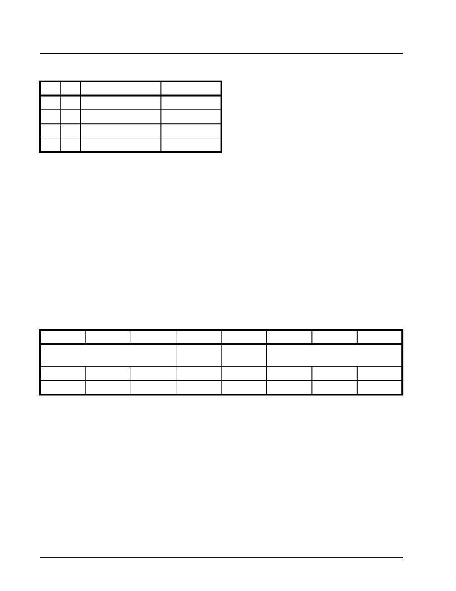
XRT7250
DS3/E3 FRAMER IC
·Á
·Á
·Á
·Á
REV. 1.1.1
66
tween these two bit-fields and the LAPD Message
Type follows:
Bit 3 - RxCR (Command/Response) Type
This Read Only bit field indicates the value of the C/R
(Command/Response) bit-field of the latest received
LAPD Message.
Bit 2 - Rx FCS (Frame Check Sequence) Error
This Read-Only bit-field indicates whether or not the
LAPD Receiver has detected a Frame Check Se-
quence (FCS) error in the newly received LAPD Mes-
sage Frame. A "0" in this bit-field indicates that the
FCS for the latest received LAPD Message Frame is
correct. A "1" in this bit-field indicates that the FCS
for the latest received LAPD Message Frame is incor-
rect.
N
OTE
: For more information on the LAPD Receiver, please
see Section 3.3.3.2.
Bit 1 - End Of Message
This Read-Only bit-field indicates whether or not the
LAPD Receiver has completed its reception of the lat-
est incoming LAPD Message frame. The local µP
can poll the progress of the LAPD Receiver by peri-
odically reading this bit-field.
A "0" in this bit-field indicates that the LAPD Receiver
is still receiving the latest message from the far end
LAPD Transmitter. A "1" in this bit-field indicates that
the LAPD Receiver has finished receiving the com-
plete LAPD Message Frame.
Bit 0 - Flag Present
This Read-Only bit-field indicates whether or not the
LAPD Receiver has detected the occurrence of the
Flag Sequence byte (0x7E). A "0" in this bit-field indi-
cates that the LAPD Receiver does not detect the oc-
currence of the Flag Sequence byte. A "1" in this bit-
field indicates that the LAPD Receiver does detect
the occurrence of the Flag Sequence byte.
N
OTE
: For more information on the LAPD Receiver, please
see Section 3.3.3.2.
2.3.3
Receive E3 Framer Configuration Regis-
ters (ITU-T G.832)
2.3.3.1
Receive E3 Configuration & Status
Register 1 (E3, ITU-T G.832)
Bit 7 - 5 - RxPLDType[2:0] (Received Payload
Type[2:0])
These three Read-Only bit-fields contain the Payload
Type value within the MA byte of the most recently re-
ceived E3 frame.
N
OTE
: The Payload Type Mismatch interrupt will be gener-
ated if the contents of these bit-fields differ from that of the
Expected Payload Types in Bits 2 through 0 within this Reg-
ister.
Bit 4 - RxFERF Algo
This Read/Write bit-field allows the user to select one
of the two RxFERF Declaration Algorithms:
Writing a "0" to this bit-field selects the following
RxFERF Declaration algorithm:
∑ The Receive E3 Framer declares a Far End
Receive Failure (FERF) if the FERF bit-field, within
the MA byte is set to "1" for 3 consecutive incoming
E3 Frames. Likewise, the Receive E3 Framer will
negate the Far End Receive Failure condition if the
FERF bit-field, within the MA byte is set to "0" for 3
consecutive incoming E3 Frames.
Writing a "1" to this bit-field selects the following
RxFERF Declaration algorithm:
∑ The Receive E3 Framer declares a Far End
Receive Failure (FERF) if the FERF bit-field, within
the MA byte is set to "1" for 5 consecutive E3
Frames. Likewise, the Receive E3 Framer will
negate the Far End Receive Failure condition if the
FERF bit-field, within the MA byte is set to "0" for 5
consecutive incoming E3 Frames.
B
IT
5 B
IT
4
M
ESSAGE
T
YPE
M
ESSAGE
LENGTH
Test Signal Identification
76 Bytes
0
1
Idle Signal Identification
76 Bytes
CL Path Identification
76 Bytes
ITU-T Path Identification
82 Bytes
RXE3 CONFIGURATION & STATUS REGISTER 1 (ADDRESS = 0X10)
B
IT
7
B
IT
6
B
IT
5
B
IT
4
B
IT
3
B
IT
2
B
IT
1
B
IT
0
RxPLDType[2:0]
RxFERF
Algo
RxTMark
Algo
RxPLDExp[2:0]
RO
RO
RO
RO
RO
R/W
R/W
R/W
0
0
0
0
0
0
0
0

·Á
·Á
·Á
·Á
DS3/E3 FRAMER IC
XRT7250
REV. 1.1.1
67
Bit 3 - RxTMark Algorithm
This Read/Write bit-field allows the user to select the
number of consecutive incoming E3 frames, that the
Timing Marker bit-field (within the MA byte-field) must
be of a given logic state, before it is validated by the
Receive E3 Framer. Once the Receive E3 Framer
has validated the state of the Timing Marker bit-field,
then it will write this logic state into Bit 1 (RxTMark)
within the Rx E3 Configuration & Status Register 2
(Address = 0x11)
Writing a "0" into this bit-field causes the Receive E3
Framer to validate the Timing Marker value after re-
ceiving 3 consecutive incoming E3 frames, with the
Timing Marker bit-field of a given value. Writing a "1"
into this bit-field causes the Receive E3 Framer to
validate the Timing Marker value after receiving 5
consecutive incoming E3 frames, with the Timing
Marker bit-field of a given value.
Bits 2 - 0: RxPLDExp[2:0]
This Read/Write bit-field allows the user to specify the
Payload Type that is expected in the MA bytes, of
each incoming E3 frame.
If the Receive E3 Framer detects a Payload Type that
differs from the values within these bit-fields, then the
Framer will generate the Payload Type Mismatch in-
terrupt.
2.3.3.2
Receive E3 Configuration & Status
Register 2 (E3, ITU-T G.832)
Bit 7 - RxLOF Algo (Loss of Frame Declaration Al-
gorithm)
This Read/Write bit-field allows the user to select the
LOF (Loss of Frame) Declaration criteria, that will be
used by the Receive E3 Framer. Writing a "0" to this
bit-field configures the Receive E3 Framer to declare
an LOF condition, after it has been in the OOF condi-
tion for 24 frame periods (3 ms). Writing a "1" to this
bit-field configures the Receive E3 Framer to declare
an LOF condition, after it has been in the OOF condi-
tion for 8 frame periods (1 ms).
Bit 6 - RxLOF (Loss of Frame Declaration)
This Read-Only bit-field indicates whether or not the
Receive E3 Framer is currently in the Loss of Frame
(LOF) condition. If this bit-field is set to "1", then the
Receive E3 Framer is currently in the LOF condition.
Conversely, if this bit-field is set to "0", then the Re-
ceive E3 Framer is currently not in the LOF condition.
Bit 5 - RxOOF (Out of Frame Declaration)
This Read-Only bit field indicates whether or not the
Receive E3 Framer is currently experiencing an Out
of Frame (OOF) condition. The Receive E3 Framer
will declare an OOF condition if it has detected errors
in the frame alignment bytes (FA1 and FA2) in four
consecutive frames. If this bit-field is set to "1", then
the Receive E3 Framer has declared, and is continu-
ing to experience an OOF condition. If this bit-field is
set to "0", then the Receive E3 Framer is currently not
experiencing an OOF condition.
Bit 4 - RxLOS (Loss of Signal Declaration)
This Read-Only bit-field indicates whether or not the
Receive E3 Framer is currently experiencing a Loss
of Signal (LOS) condition. The Receive E3 Framer
will declare an LOS condition if it has detected a
string of 32 consecutive "0's", via the RxPOS and Rx-
NEG input pins. If this bit-field is set to "1", then the
Receive E3 Framer has declared, and is continuing to
experience an LOS condition. If this bit-field is set to
"0", then the Receive E3 Framer is currently not expe-
riencing an LOS condition.
Bit 3 - RxAIS (Alarm Indication Status Declara-
tion)
This Read-Only bit-field indicates whether or not the
Receive E3 Framer is currently experiencing an AIS
condition. The Receive E3 Framer will declare an
AIS condition if it has detected two consecutive E3
frames, that each contain less than seven (7) "0's" . If
this bit-field is set to "1", then the Receive E3 Framer
has declared, and is continuing to experience an AIS
condition. If this bit-field is set to "0", then the Re-
ceive E3 Framer is currently not experiencing an AIS
condition.
Bit 2 - RxPLDType UnStab
This Read-Only bit-field indicates whether or not the
Receive E3 Framer has been receiving a consistent
RXE3 CONFIGURATION & STATUS REGISTER 2 (ADDRESS = 0X11)
B
IT
7
B
IT
6
B
IT
5
B
IT
4
B
IT
3
B
IT
2
B
IT
1
B
IT
0
Rx LOF Algo
RxLOF
RxOOF
RxLOS
RxAIS
RxPld Unstab
RxTMark
RxFERF
R/W
RO
RO
RO
RO
RO
RO
RO
0
1
1
1
1
1
1
1

XRT7250
DS3/E3 FRAMER IC
·Á
·Á
·Á
·Á
REV. 1.1.1
68
Payload Type value (within the MA Byte-Field) in the
last 5 consecutive incoming E3 frames.
If the Receive E3 Framer has detected a change in
the Payload Type value, within the last 5 incoming E3
frames, then it will set this bit-field to "1". If the Pay-
load Type value has been consistent in the last 5 E3
frames, then the Receive E3 Framer will set this bit-
field to "0".
Bit 1 - Rx TMark
This Read-Only bit-field reflects the most recently val-
idated Timing Marker value. The Receive E3 Framer
will validate the Timing Marker state, after it has de-
tected a user-selectable number of consecutive in-
coming E3 frames with a consistent Timing Marker
value. The user makes this selection by writing the
appropriate value to Bit 3 (RxTMarkAlgo) within the
Rx E3 Configuration/Status Register (Address =
0x0E).
Bit 0 - RxFERF (Far End Receive Failure)
This Read-Only bit-field indicates whether or not the
Receive E3 Framer is experiencing an FERF (Far-
End-Receive-Failure) condition. The Receive E3
Framer will declare a FERF condition, if it has re-
ceived a user-selectable number of consecutive E3
frames, with the FERF bit-field (within the MA byte)
set to "1". This user-selectable number is either 3 or
5 E3 frames. Conversely, the Receive E3 Framer will
negate the FERF declaration, if it has received this
user-selectable number of consecutive E3 frames,
with the FERF bit-field set to "0".
If this bit-field is set to "1", then the Receive E3 Fram-
er has declared an FERF condition. If this bit-field is
set to "0", then the Receive E3 Framer has not de-
clared an FERF condition.
N
OTE
: Please see Section 5.1.1.4, for a more detailed dis-
cussion on the meaning of the FERF bit-field, within the E3
frame.
2.3.3.3
3.3.2.17 Receive E3 Interrupt Enable
Register (E3, ITU-T G.832)
Bit 4 - Change of Frame Alignment (COFA) Inter-
rupt Enable
This Read/Write bit-field allows the user to enable or
disable the Change of Frame Alignment interrupt.
Setting this bit-field to "1" enables this interrupt. Set-
ting this bit-field to "0" disables this interrupt.
Bit 3 - OOF (Out of Frame) Interrupt Enable
This Read/Write bit field allows the user to enable or
disable the Change in Out-of-Frame (OOF) status in-
terrupt. Setting this bit-field to "1" enables this inter-
rupt. Setting this bit-field to "0" disables this interrupt.
N
OTE
: For more information on the OOF Condition, please
see Section 5.3.2.1.
Bit 2 - LOF (Loss of Frame) Interrupt Enable
This Read/Write bit-field allows the user to enable or
disable the Change in Loss-of-Frame (LOF) status in-
terrupt. Setting this bit-field to "1" enables this inter-
rupt. Setting this bit-field to "0" disables this interrupt.
For more information on the LOF Condition, please
see Section 5.3.2.1.
Bit 1 - LOS (Loss of Signal) Interrupt Enable
This Read/Write bit-field allows the user to enable or
disable the Change in LOS condition interrupt. Set-
ting this bit-field to "1" enables this interrupt. Setting
this bit-field to "0" disables this interrupt.
N
OTE
: For more information on the LOS Condition, please
see Section 5.3.2.6.
Bit 0 - AIS Interrupt Enable
This Read/Write bit-field allows the user to enable or
disable the Change in AIS condition interrupt. Setting
this bit-field to "1" enables this interrupt. Setting this
bit-field to "0" disables this interrupt.
N
OTE
: For more information on the AIS Condition, please
see Section 5.3.2.6.2.
RXE3 INTERRUPT ENABLE REGISTER - 1 (ADDRESS = 0X12)
B
IT
7
B
IT
6
B
IT
5
B
IT
4
B
IT
3
B
IT
2
B
IT
1
B
IT
0
Not Used
COFA
Interrupt
Enable
OOF
Interrupt
Enable
LOF
Interrupt
Enable
LOS
Interrupt
Enable
AIS
Interrupt
Enable
RO
RO
RO
R/W
R/W
R/W
R/W
R/W
0
0
0
0
0
0
0
0

·Á
·Á
·Á
·Á
DS3/E3 FRAMER IC
XRT7250
REV. 1.1.1
69
2.3.3.4
3.3.2.18 Receive E3 Interrupt Enable
Register - 2 (E3, ITU-T G.832)
Bit 6 - TTB Change Interrupt Enable
This Read/Write bit-field allows the user to enable or
disable the Change in Trail Trace Buffer Message in-
terrupt. Setting this bit-field to "1" enables this inter-
rupt. Setting this bit-field to "0" disables this interrupt.
N
OTE
: For more information on Trail Trace Buffer mes-
sages, please see Section 5.3.2.9.
Bit 5 - Received LAPD Message Interrupt Enable
This Read/Write bit-field allows the user to enable or
disable the Received LAPD Message frame interrupt.
Setting this bit-field to "1" enables this interrupt. Set-
ting this bit-field to "0" disables this interrupt.
N
OTE
: For more information on this interrupt, please see
Section 5.3.6.1.12.
Bit 4 - FEBE (Far-End Block Error) Interrupt En-
able
This Read/Write bit-field allows the user to enable or
disable the Far-End-Block Error (FEBE) interrupt.
Setting this bit-field to "1" enables this interrupt. Set-
ting this bit-field to "0" disables this interrupt.
N
OTE
: For more information on the FEBE Interrupt condi-
tion, please see Section 5.3.6.1.8.
Bit 3 - FERF (Far-End Receive Failure) Interrupt
Enable
This Read/Write bit-field allows the user to enable or
disable the Change in FERF Condition interrupt. Set-
ting this bit-field to "1" enables this interrupt. Setting
this bit-field to "0" disables this interrupt.
N
OTE
: For more information on the Change in FERF Condi-
tion interrupt, please see Section 5.3.6.1.7.
Bit 2 - EM Byte Error Interrupt Enable
This Read/Write bit-field allows the user to enable or
disable the EM Byte Error interrupt. Setting this bit-
field to "1" enables this interrupt. Setting this bit-field
to "0" disables this interrupt.
N
OTE
: For more information on this interrupt, please see
Section 5.3.6.1.9.
Bit 1 - Framing Byte Error Interrupt Enable
This Read/Write bit-field allows the user to enable or
disable the Framing Byte Error interrupt. Setting this
bit-field to "1" enables this interrupt. Setting this bit-
field to "0" disables this interrupt.
N
OTE
: For more information on this interrupt, please see
Section 5.3.6.1.10.
Bit 0 - Receive Payload Type Mismatch Interrupt
Enable
This Read/Write bit-field allows the user to enable or
disable the Receive Payload Type Mismatch interrupt.
Setting this bit-field to "1" enables this interrupt. Set-
ting this bit-field to "0" disables this interrupt.
N
OTE
: For more information on this interrupt, please see
Section 5.3.6.1.11.
2.3.3.5
Receive E3 Interrupt Status Register -
1 (E3, ITU-T G.832)
RXE3 INTERRUPT ENABLE REGISTER - 2 (ADDRESS = 0X13)
B
IT
7
B
IT
6
B
IT
5
B
IT
4
B
IT
3
B
IT
2
B
IT
1
B
IT
0
Not Used
TTB
Change
Interrupt
Enable
Not Used
FEBE
Interrupt
Enable
FERF
Interrupt
Enable
BIP-8
Error Interrupt
Enable
Framing
Byte Error
Interrupt
Enable
RxPld
Mis
Interrupt
Enable
RO
R/W
RO
R/W
R/W
R/W
R/W
R/W
0
0
0
0
0
0
0
0
RXE3 INTERRUPT STATUS REGISTER - 1 (ADDRESS = 0X14)
B
IT
7
B
IT
6
B
IT
5
B
IT
4
B
IT
3
B
IT
2
B
IT
1
B
IT
0
Not Used
COFA
Interrupt
Status
OOF
Interrupt
Status
LOF
Interrupt
Status
LOS
Interrupt
Status
AIS
Interrupt
Status
RO
RO
RO
RUR
RUR
RUR
RUR
RUR
0
0
0
0
0
0
0
0

XRT7250
DS3/E3 FRAMER IC
·Á
·Á
·Á
·Á
REV. 1.1.1
70
Bit 4 - COFA (Change of Frame Alignment) Inter-
rupt Status
This Reset-upon-Read bit-field will be set to "1" if the
Change of Frame Alignment interrupt has occurred
since the last read of this register.
The Receive E3 Framer will generate the Change of
Frame Alignment interrupt if it has detected a change
in frame alignment in the incoming E3 frames.
Bit 3 - OOF (Receive E3 Framer) Interrupt Status
This Reset Upon Read bit-field is set to "1" if the Re-
ceive E3 Framer has detected a Change in the Out-
of-Frame (OOF) Condition, since the last time this
register was read. Therefore, this bit-field will be as-
serted under either of the following two conditions:
1. When the Receive E3 Framer has detected the
appropriate conditions to declare an OOF Condi-
tion.
2. When the Receive E3 Framer has transitioned
from the OOF Condition (Frame Acquisition
Mode) into the In-Frame Condition (Frame Main-
tenance mode).
N
OTE
: For more information of the OOF Condition, please
see Section 5.3.2.1.
Bit 2 - LOF (Loss of Frame) Interrupt Status
This Reset-upon-Read bit-field will be set to "1" if a
Change in LOF Condition interrupt has occurred
since the last read of this register.
The Receive E3 Framer will generate the Change in
LOF Condition interrupt is response to either of the
following two occurrences.
1. Whenever the Receive E3 Framer transitions
from the OOF Condition state into the LOF Con-
dition state, within the E3 Framing Acquisition/
Maintenance algorithm (per Figure 194).
2. Whenever the Receive E3 Framer transitions
from the FA1, FA2 Octet Verification state to the
In-frame state, within the E3 Framing Acquisition/
Maintenance algorithm (per Figure 194).
Bit 1 - LOS (Loss of Signal) Interrupt Status
This Reset Upon Read bit will be set to "1", if the Re-
ceive E3 Framer has detected a
Change in the LOS Status condition, since the last
time this register was read. This bit-field will be as-
serted under either of the following two conditions:
1. When the Receive E3 Framer detects the occur-
rence of an LOS Condition (e.g., the occurrence
of 32 consecutive spaces in the incoming E3 data
stream), and
2. When the Receive E3 Framer detects the end of
an LOS Condition (e.g., when the Receive E3
Framer detects a string 32 bits that does not con-
tain a string of four consecutive "0's").
The local µP can determine the current state of the
LOS condition by reading bit 6 of the Rx E3 Configu-
ration and Status Register (Address = 0x11).
N
OTE
: For more information in the LOS of Signal (LOS)
Alarm, please see Section 5.3.2.6.
Bit 0 - AIS Interrupt Status
This Reset Upon Read bit field will be set to "1", if the
Receive E3 Framer has detected a Change in the AIS
condition, since the last time this register was read.
This bit-field will be asserted under either of the fol-
lowing two conditions:
1. When the Receive E3 Framer first detects an AIS
Condition in the incoming E3 data stream.
2. When the Receive E3 Framer has detected the
end of an AIS Condition in the incoming E3 data
stream.
The local µP can determine the current state of the
AIS condition by reading bit 7 of the Rx E3 Configura-
tion and Status Register (Address = 0x11).
N
OTE
: For more information on the AIS Condition please
see Section 5.3.2.6.2.
2.3.3.6
Receive E3 Interrupt Status Register -
2 (E3, ITU-T G.832)
Bit 6 - TTB Change Interrupt Status (Receipt of
New Trail Trace Buffer Message interrupt)
RXE3 INTERRUPT STATUS REGISTER - 2 (ADDRESS = 0X15)
B
IT
7
B
IT
6
B
IT
5
B
IT
4
B
IT
3
B
IT
2
B
IT
1
B
IT
0
Not Used
TTB
Change
Interrupt
Status
Not Used
FEBE
Interrupt
Status
FERF
Interrupt
Status
BIP-8
Error Interrupt
Status
Framing
Byte Error
Interrupt
Status
RxPld
Mis
Interrupt
Status
RO
RUR
RO
RUR
RUR
RUR
RUR
RUR
0
0
0
0
0
0
0
0

·Á
·Á
·Á
·Á
DS3/E3 FRAMER IC
XRT7250
REV. 1.1.1
71
This Reset-upon-Read bit-field will be set to "1" if a
Receipt of New Trail Trace Buffer Message interrupt
has occurred since the last read of this register.
The Receive E3 Framer will generate the Receipt of
New Trail Trace Buffer Message interrupt, if it receives
an E3 frame in which the value of the TR byte-field is
of the form "1xxxxxxxb". A TR byte-field value of this
form is identified as the frame start marker.
N
OTE
: Please see Section 5.3.6.1.6 for a more detailed dis-
cussion of this interrupt.
Bit 4 - FEBE (Far-End Block Error) Interrupt Status
This Reset-upon-Read bit-field will be set to "1" if the
FEBE (Far-End-Block Error) interrupt has occurred
since the last read of this register.
The Receive E3 Framer will generate the FEBE inter-
rupt anytime it detects a "1" in the FEBE bit-field with-
in an incoming E3 frame.
N
OTE
: Please see Section 5.3.6.1.8 for a more detailed dis-
cussion of this interrupt.
Bit 3 - FERF Interrupt Status
This Reset Upon Read bit will be set to '1' if the Re-
ceive E3 Framer has detected a Change in the Rx
FERF Condition, since the last time this register was
read.
This bit-field will be asserted under either of the fol-
lowing two conditions.
1. When the Receive E3 Framer first detects the
occurrence of an RxFERF Condition (e.g., when
the FERF bit, within the last 3 or 5 consecutive
E3 frames are set to "1").
2. When the Receive E3 Framer detects the end of
the RxFERF Condition (e.g., when the FERF bit,
within the last 3 or 5 consecutive E3 frames are
set to "0").
N
OTE
: For more information on the RxFERF (Yellow Alarm)
condition, please see Section 5.3.2.6.3.
Bit 2 - EM (BIP-8) Byte Error Interrupt Status
This Reset-upon-Read bit-field will be set to "1" if the
BIP-8 Error interrupt has occurred since the last read
of this register.
The Receive E3 Framer will generate the BIP-8 Error
interrupt if it has concluded that it has received an er-
rored E3 frame, from the Far-End Terminal.
N
OTE
: Please see Section 5.3.6.1.9 for a more detailed dis-
cussion of this interrupt.
Bit 1 - Framing Byte Error Interrupt Status
This Reset-upon-Read bit-field will be set to "1" if the
Framing Byte Error interrupt has occurred since the
last read of this register.
The Receive E3 Framer will generate the Framing
Byte Error interrupt if it has detected an error in the
FA1 or FA2 bytes, on an incoming E3 frame.
N
OTE
: Please see Section 5.3.6.1.10 for a more detailed
discussion of this interrupt.
Bit 0 - Rx Pld Mis Interrupt Status
This Reset-upon-Read bit-field will be set to "1" if the
Payload Type Mismatch interrupt has occurred since
the last read of this register.
The Receive E3 Framer will generate the Payload
Type Mismatch interrupt when it detects that the val-
ues, within the Payload Type bit-fields of the incoming
E3 frame, has changed from that of the previous E3
frame.
N
OTE
: Please see Section 5.3.6.1.11 for a more detailed
discussion on this interrupt.
2.3.3.7
Receive E3 LAPD Control Register (E3,
ITU-T G.832)
Bit 3 - DL from NR
This Read/Write bit-field allows the user to specify
whether the LAPD Receiver should retrieve the bytes,
comprising the incoming LAPD Message frame, from
the NR byte-field, or from the GC byte-field, within
each incoming E3 frame.
Writing a "1" configures the LAPD Receiver to re-
trieve the incoming LAPD Message frame octets from
the NR byte-field, within each incoming E3 frame.
Writing a "0" configures the LAPD Receiver to re-
trieve the incoming LAPD Message frame octets from
the GC byte.
RXE3 LAPD CONTROL REGISTER (ADDRESS = 0X18)
B
IT
7
B
IT
6
B
IT
5
B
IT
4
B
IT
3
B
IT
2
B
IT
1
B
IT
0
Not Used
DL from NR
RxLAPD
Enable
RxLAPD
Interrupt
Enable
RxLAPD
Interrupt
Status
RO
RO
RO
RO
R/W
R/W
R/W
RUR
0
0
0
0
0
0
0
0

XRT7250
DS3/E3 FRAMER IC
·Á
·Á
·Á
·Á
REV. 1.1.1
72
Bit 2 - RxLAPD Enable
This Read/Write bit-field allows the user to enable or
disable the LAPD Receiver, for reception of incoming
LAPD Message frames from the Remote LAPD
Transmitter.
Writing a "1" to this bit-field enables the LAPD Re-
ceiver. Writing a "0" to this bit-field disables the LAPD
Receiver.
Bit 1 - RxLAPD (Received LAPD Message) Inter-
rupt Enable
This Read/Write bit-field allows the user to enable or
disable the Received LAPD Message frame interrupt.
Setting this bit-field to "1" enables this interrupt. Set-
ting this bit-field to "0" disables this interrupt. For
more information on this interrupt, please see Section
5.3.3.
Bit 0 - RxLAPD (Received LAPD Message) Inter-
rupt Status
This Reset-upon-Read bit-field will be set to "1" if the
Receipt of New LAPD Message frame interrupt has
occurred since the last read of this register.
The Receive E3 Framer will generate this Receipt of
New LAPD Message frame interrupt when the LAPD
Receiver has received a complete LAPD Message
frame from the Remote LAPD Transmitter.
N
OTE
: Please see section 5.3.6.1.12 for a more detailed
discussion of this interrupt.
2.3.3.8
Receive E3 LAPD Status Register (E3,
ITU-T G.832
Bit 6 - Rx Abort
This Read-Only bit-field indicates whether or not the
LAPD Receiver is currently detecting an abort se-
quence (e.g., a string of 7 consecutive "1's").
This bit-field is set to "1" if the LAPD Receiver is cur-
rently detecting an abort sequence in the incoming
LAPD Channel. Conversely, this bit-field is set to "0"
if the LAPD Receiver has not detected an abort se-
quence, since the last read of this register.
Bit 5, 4 - RxLAPD Type[1:0]
These two Read-Only bit-fields combine to indicate
the type and size of LAPD Message frame that has
been received by the LAPD Receiver. The following
table relates the contents of these bit-fields to the
LAPD Message type/size.
Bit 3 - Rx CR Type
This Read-Only bit-field indicates the state of the C/R
bit-field, within octet # 2 of the most recently received
LAPD Message frame.
Bit 2 - Rx FCS Error
This Read-Only bit-field indicates whether or not the
LAPD Receiver has detected an FCS (Frame Check
Sequence) error, in the most recently received LAPD
Message frame. This bit-field is set to "0" if the LAPD
Receiver does not detect an FCS error in this LAPD
Message frame. Conversely, this bit-field is set to "1"
if the LAPD Receiver does detect an FCS error in this
LAPD Message frame.
RXE3 LAPD STATUS REGISTER (ADDRESS = 0X19)
B
IT
7
B
IT
6
B
IT
5
B
IT
4
B
IT
3
B
IT
2
B
IT
1
B
IT
0
Not Used
Rx ABORT
RxLAPDType[1:0]
RxCR
Type
RxFCS
Error
End of
Message
Flag
Present
RO
RO
RO
RO
R/W
R/W
R/W
RUR
0
0
0
0
0
0
0
0
R
X
LAPDT
YPE
[1:0]
LAPD M
ESSAGE
F
RAME
T
YPE
PMDL M
ESSAGE
S
IZE
(I
NFORMATION
S
ECTION
)
00
Test Signal Identification Type
76 Bytes
01
Idle Signal Identification Type
76 Bytes
10
CL Path Identification Type
76 Bytes
11
ITU-T Path Identification Type
82 Bytes
·Á
·Á
·Á
·Á
DS3/E3 FRAMER IC
XRT7250
REV. 1.1.1
73
N
OTE
: For a more detailed discussion on the LAPD
Receiver's handling of the FCS bytes, please see Section
5.3.3.
Bit 1 - EndOfMessage
The LAPD Receiver will assert this read-only bit-field,
when it has received a complete LAPD Message
frame. This bit-field, along with the Receipt of New
LAPD Message frame interrupt, serves to inform the
local µP that the Receive LAPD Message buffer con-
tains a new PMDL message that needs to be read
and processed.
This bit-field is cleared (to "0") upon reading this reg-
ister.
Bit 0 - Flag Present
The LAPD Receiver will assert this read-only bit-field
when it is currently detecting the Flag Sequence octet
(7Eh) in the incoming LAPD channel (e.g., either the
GC or the NR byte-field, within each E3 frame). The
LAPD Receiver will negate this bit-field when it is no
longer receiving the Flag Sequence octet in the in-
coming LAPD channel.
2.3.3.9
Receive E3 NR Byte Register (E3, ITU-T
G.832)
This Read-Only register contains the value of the NR
byte, within the most recently received E3 frame.
Please see Section 5.3.3 for a more detailed discus-
sion on this register.
2.3.3.10 Receive E3 GC Byte Register (E3, ITU-
T G.832)
This Read-Only register contains the value of the GC
byte, residing in the most recently received E3 frame.
Please see Section 5.3.3 for a more detailed discus-
sion on this register.
2.3.3.11 Receive E3 TTB-0 Register (E3, ITU-T
G.832)
This Read-Only register contains the frame start
marker byte of the 16 byte Trail Trace Buffer Message
that has been received from the Far-End Terminal, via
the TR byte-field within the incoming E3 frames. The
remaining bytes, of this Trail Trace Buffer Message
can be found in the RxTTB-1 through RxTTB-15 reg-
isters.
The data in this register is typically of the form [1, C6,
C5, C4, C3, C2, C1, C0]. The "1" in the MSB position
identifies this byte as being the frame start marker
RXE3 NR BYTE REGISTER (ADDRESS = 0X1A)
B
IT
7
B
IT
6
B
IT
5
B
IT
4
B
IT
3
B
IT
2
B
IT
1
B
IT
0
RxNR[7:0]
RO
RO
RO
RO
RO
RO
RO
RO
0
0
0
0
0
0
0
0
RXE3 GC BYTE REGISTER (ADDRESS = 0X1B)
B
IT
7
B
IT
6
B
IT
5
B
IT
4
B
IT
3
B
IT
2
B
IT
1
B
IT
0
RxGC[7:0]
RO
RO
RO
RO
RO
RO
RO
RO
0
0
0
0
0
0
0
0
RXE3 TTB-0 REGISTER (ADDRESS = 0X1C)
B
IT
7
B
IT
6
B
IT
5
B
IT
4
B
IT
3
B
IT
2
B
IT
1
B
IT
0
RxTTB-0
RO
RO
RO
RO
RO
RO
RO
RO
0
0
0
0
0
0
0
0
XRT7250
DS3/E3 FRAMER IC
·Á
·Á
·Á
·Á
REV. 1.1.1
74
(e.g., the first byte within the 16 byte Trail Trace Buffer
Message). The remaining bits: C0 - C6 contain the
CRC-7 value that was calculated over the previous 16
byte Trail Trace Buffer Message.
N
OTES
:
1. The XRT7250 Framer device will not compute or
verify this CRC-7 value. It is up to the user's hard-
ware and/or software to compute and verify this
value.
2. For more information on the use of this register,
please see Section 5.3.2.9.
2.3.3.12 Receive E3 TTB-1 Register (E3, ITU-T
G.832)
This Read-Only register contains the second (2nd)
byte within the 16 byte Trail Trace Buffer Message,
that has been received from the Far-End Terminal.
This register typical contains an ASCII character that
is required for the E.164 numbering format.
N
OTE
: For more information on the use of this register,
please see Section 5.3.2.9.
2.3.3.13 Receive E3 TTB-2 Register (E3, ITU-T
G.832)
This Read-Only register contains the third (3rd) byte
within the 16 byte Trail Trace Buffer Message, that
has been received from the Far-End Terminal. This
register typical contains an ASCII character that is re-
quired for the E.164 numbering format.
N
OTE
: For more information on the use of this register,
please see Section 5.3.2.9.
2.3.3.14 Receive E3 TTB-3 Register (E3, ITU-T
G.832)
This Read-Only register contains the fourth (4th) byte
within the 16 byte Trail Trace Buffer Message, that
has been received from the Far-End Terminal. This
register typical contains an ASCII character that is re-
quired for the E.164 numbering format.
N
OTE
: For more information on the use of this register,
please see Section 5.3.2.9.
RXE3 TTB-1 REGISTER (ADDRESS = 0X1D)
B
IT
7
B
IT
6
B
IT
5
B
IT
4
B
IT
3
B
IT
2
B
IT
1
B
IT
0
RxTTB-1
RO
RO
RO
RO
RO
RO
RO
RO
0
0
0
0
0
0
0
0
RXE3 TTB-2 REGISTER (ADDRESS = 0X1E)
B
IT
7
B
IT
6
B
IT
5
B
IT
4
B
IT
3
B
IT
2
B
IT
1
B
IT
0
RxTTB-2
RO
RO
RO
RO
RO
RO
RO
RO
0
0
0
0
0
0
0
0
RXE3 TTB-3 REGISTER (ADDRESS = 0X1F)
B
IT
7
B
IT
6
B
IT
5
B
IT
4
B
IT
3
B
IT
2
B
IT
1
B
IT
0
RxTTB-3
RO
RO
RO
RO
RO
RO
RO
RO
0
0
0
0
0
0
0
0

·Á
·Á
·Á
·Á
DS3/E3 FRAMER IC
XRT7250
REV. 1.1.1
75
2.3.3.15 Receive E3 TTB-4 Register (E3, ITU-T
G.832)
This Read-Only register contains the fifth (5th) byte
within the 16 byte Trail Trace Buffer Message, that
has been received from the Far-End Terminal. This
register typical contains an ASCII character that is re-
quired for the E.164 numbering format.
N
OTE
: For more information on the use of this register,
please see Section 5.3.2.9.
2.3.3.16 Receive E3 TTB-5 Register (E3, ITU-T
G.832)
This Read-Only register contains the sixth (6th) byte
within the 16 byte Trail Trace Buffer Message, that
has been received from the Far-End Terminal. This
register typical contains an ASCII character that is re-
quired for the E.164 numbering format.
N
OTE
: For more information on the use of this register,
please see Section 5.3.2.9.
2.3.3.17 Receive E3 TTB-6 Register (E3, ITU-T
G.832)
This Read-Only register contains the seventh (7th)
byte within the 16 byte Trail Trace Buffer Message,
that has been received from the Far-End Terminal.
This register typical contains an ASCII character that
is required for the E.164 numbering format.
N
OTE
: For more information on the use of this register,
please see Section 5.3.2.9.
2.3.3.18 Receive E3 TTB-7 Register (E3, ITU-T
G.832)
RXE3 TTB-4 REGISTER (ADDRESS = 0X20)
B
IT
7
B
IT
6
B
IT
5
B
IT
4
B
IT
3
B
IT
2
B
IT
1
B
IT
0
RxNR[7:0]
RO
RO
RO
RO
RO
RO
RO
RO
0
0
0
0
0
0
0
0
RXE3 TTB-5 REGISTER (ADDRESS = 0X21)
B
IT
7
B
IT
6
B
IT
5
B
IT
4
B
IT
3
B
IT
2
B
IT
1
B
IT
0
RxTTB-5
RO
RO
RO
RO
RO
RO
RO
RO
0
0
0
0
0
0
0
0
RXE3 TTB-6 REGISTER (ADDRESS = 0X22)
B
IT
7
B
IT
6
B
IT
5
B
IT
4
B
IT
3
B
IT
2
B
IT
1
B
IT
0
RxNR[7:0]
RO
RO
RO
RO
RO
RO
RO
RO
0
0
0
0
0
0
0
0
RXE3 TTB-7 REGISTER (ADDRESS = 0X23)
B
IT
7
B
IT
6
B
IT
5
B
IT
4
B
IT
3
B
IT
2
B
IT
1
B
IT
0
RxTTB-7
RO
RO
RO
RO
RO
RO
RO
RO
0
0
0
0
0
0
0
0
XRT7250
DS3/E3 FRAMER IC
·Á
·Á
·Á
·Á
REV. 1.1.1
76
This Read-Only register contains the eighth (8th) byte
within the 16 byte Trail Trace Buffer Message, that
has been received from the Far-End Terminal. This
register typical contains an ASCII character that is re-
quired for the E.164 numbering format.
N
OTE
: For more information on the use of this register,
please see Section 5.3.2.9.
2.3.3.19 Receive E3 TTB-8 Register (E3, ITU-T
G.832)
This Read-Only register contains the ninth (9th) byte
within the 16 byte Trail Trace Buffer Message, that
has been received from the Far-End Terminal. This
register typical contains an ASCII character that is re-
quired for the E.164 numbering format.
N
OTE
: For more information on the use of this register,
please see Section 5.3.2.9.
2.3.3.20 Receive E3 TTB-9 Register (E3, ITU-T
G.832)
This Read-Only register contains the tenth (10th) byte
within the 16 byte Trail Trace Buffer Message, that
has been received from the Far-End Terminal. This
register typical contains an ASCII character that is re-
quired for the E.164 numbering format.
N
OTE
: For more information on the use of this register,
please see Section 5.3.2.9.
2.3.3.21 Receive E3 TTB-10 Register (E3, ITU-T
G.832)
This Read-Only register contains the eleventh (11th)
byte within the 16 byte Trail Trace Buffer Message,
that has been received from the Far-End Terminal.
This register typical contains an ASCII character that
is required for the E.164 numbering format.
N
OTE
: For more information on the use of this register,
please see Section 5.3.2.9.
RXE3 TTB-8 REGISTER (ADDRESS = 0X24)
B
IT
7
B
IT
6
B
IT
5
B
IT
4
B
IT
3
B
IT
2
B
IT
1
B
IT
0
RxNR[7:0]
RO
RO
RO
RO
RO
RO
RO
RO
0
0
0
0
0
0
0
0
RXE3 TTB-9 REGISTER (ADDRESS = 0X25)
B
IT
7
B
IT
6
B
IT
5
B
IT
4
B
IT
3
B
IT
2
B
IT
1
B
IT
0
RxTTB-9
RO
RO
RO
RO
RO
RO
RO
RO
0
0
0
0
0
0
0
0
RXE3 TTB-10 REGISTER (ADDRESS = 0X26)
B
IT
7
B
IT
6
B
IT
5
B
IT
4
B
IT
3
B
IT
2
B
IT
1
B
IT
0
RxTTB-10
RO
RO
RO
RO
RO
RO
RO
RO
0
0
0
0
0
0
0
0
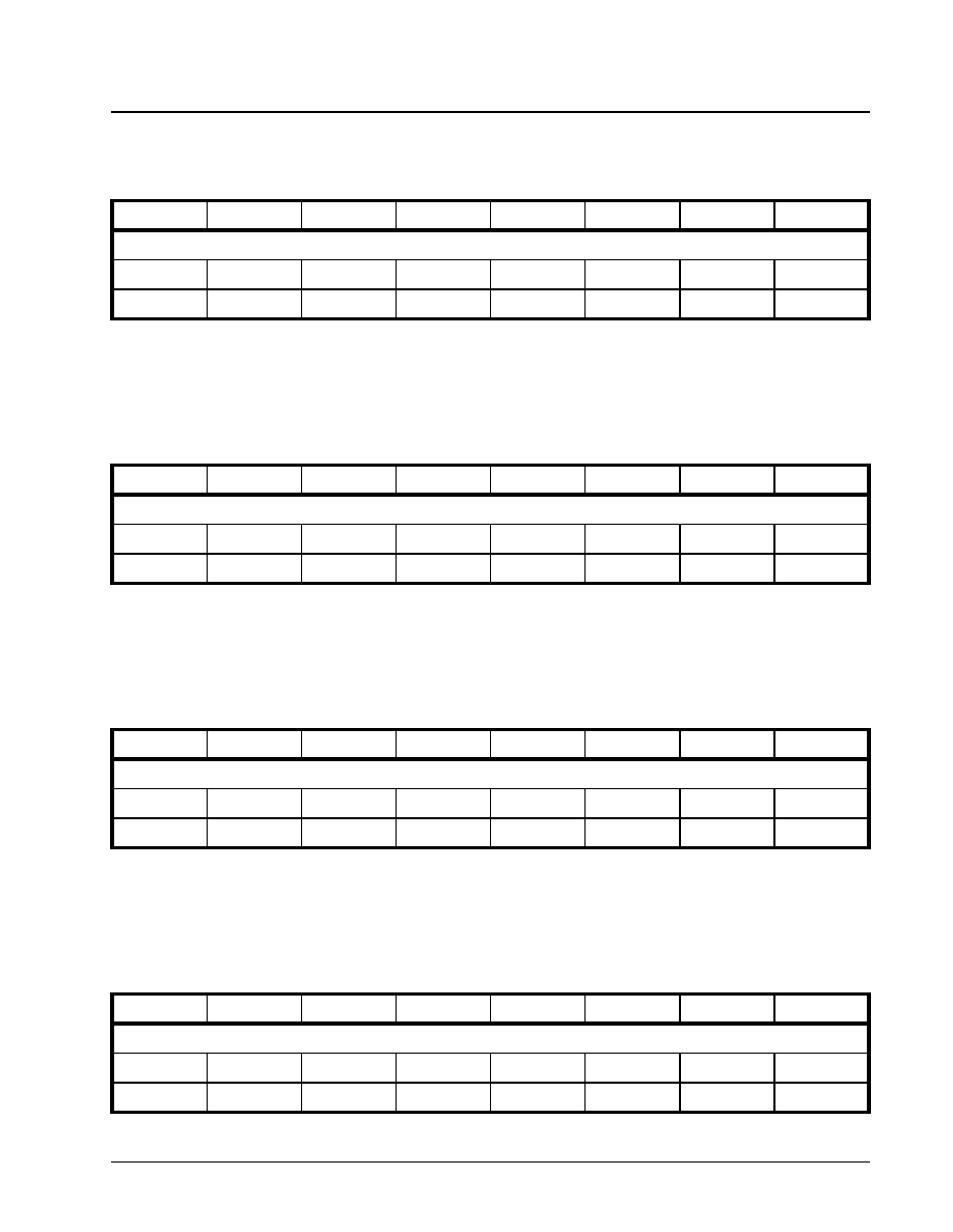
·Á
·Á
·Á
·Á
DS3/E3 FRAMER IC
XRT7250
REV. 1.1.1
77
2.3.3.22 Receive E3 TTB-11 Register (E3, ITU-T
G.832)
This Read-Only register contains the twelfth (12th)
byte within the 16 byte Trail Trace Buffer Message,
that has been received from the Far-End Terminal.
This register typical contains an ASCII character that
is required for the E.164 numbering format.
N
OTE
: For more information on the use of this register,
please see Section 5.3.2.9.
2.3.3.23 Receive E3 TTB-12 Register (E3, ITU-T
G.832)
This Read-Only register contains the thirteenth (13th)
byte within the 16 byte Trail Trace Buffer Message,
that has been received from the Far-End Terminal.
This register typical contains an ASCII character that
is required for the E.164 numbering format.
N
OTE
: For more information on the use of this register,
please see Section 5.3.2.9.
2.3.3.24 Receive E3 TTB-13 Register (E3, ITU-T
G.832)
This Read-Only register contains the fourteenth
(14th) byte within the 16 byte Trail Trace Buffer Mes-
sage, that has been received from the Far-End Termi-
nal. This register typical contains an ASCII character
that is required for the E.164 numbering format.
N
OTE
: For more information on the use of this register,
please see Section 5.3.2.9.
2.3.3.25 Receive E3 TTB-14 Register (E3, ITU-T
G.832)
RXE3 TTB-11 REGISTER (ADDRESS = 0X27)
B
IT
7
B
IT
6
B
IT
5
B
IT
4
B
IT
3
B
IT
2
B
IT
1
B
IT
0
RxTTB-11
RO
RO
RO
RO
RO
RO
RO
RO
0
0
0
0
0
0
0
0
RXE3 TTB-12 REGISTER (ADDRESS = 0X28)
B
IT
7
B
IT
6
B
IT
5
B
IT
4
B
IT
3
B
IT
2
B
IT
1
B
IT
0
RxTTB-12
RO
RO
RO
RO
RO
RO
RO
RO
0
0
0
0
0
0
0
0
RXE3 TTB-13 REGISTER (ADDRESS = 0X29
B
IT
7
B
IT
6
B
IT
5
B
IT
4
B
IT
3
B
IT
2
B
IT
1
B
IT
0
RxTTB-13
RO
RO
RO
RO
RO
RO
RO
RO
0
0
0
0
0
0
0
0
RXE3 TTB-14 REGISTER (ADDRESS = 0X2A)
B
IT
7
B
IT
6
B
IT
5
B
IT
4
B
IT
3
B
IT
2
B
IT
1
B
IT
0
RxTTB-14
RO
RO
RO
RO
RO
RO
RO
RO
0
0
0
0
0
0
0
0
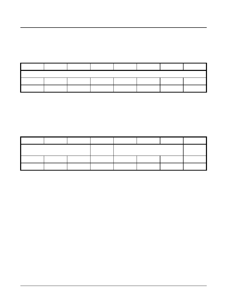
XRT7250
DS3/E3 FRAMER IC
·Á
·Á
·Á
·Á
REV. 1.1.1
78
This Read-Only register contains the fifteenth (15th)
byte within the 16 byte Trail Trace Buffer Message,
that has been received from the Far-End Terminal.
This register typical contains an ASCII character that
is required for the E.164 numbering format.
N
OTE
: For more information on the use of this register,
please see Section 5.3.2.9.
2.3.3.26 Receive E3 TTB-15 Register (E3, ITU-T
G.832)
This Read-Only register contains the sixteenth (16th)
byte within the 16 byte Trail Trace Buffer Message,
that has been received from the Far-End Terminal.
This register typical contains an ASCII character that
is required for the E.164 numbering format.
N
OTE
: For more information on the use of this register,
please see Section 5.3.2.9.
2.3.4
Receive E3 Framer Configuration Regis-
ters (ITU-T G.751)
2.3.4.1
Receive E3 Framer Configuration &
Status Register - 1 (E3, ITU-T G.751)
Bit 4 - RxFERF Algo(rithm) Select
This Read/Write bit-field permits the user to select
the Received FERF Declaration Algorithm.
Setting this bit-field to "0", configures the Receive
Section of the XRT7250 to declare a FERF (Far-End-
Receive Failure), after three (3) consecutive E3
frames, with the A-bit set to "1", have been received.
Further, the Receive Section of the XRT7250 will
clear FERF, after three (3) consecutive E3 frames,
with the A-bit set to "0", have been received.
Setting this bit-field to "1", configures the Receive
Section of the XRT7250 to declare a FERF, after five
(5) consecutive E3 frames, with the A-bit set to "1",
have been received. Further, the Receive Section of
the XRT7250 will clear FERF after five (5) consecu-
tive E3 frames, with the A-bit set to "0", have been re-
ceived.
Bit 0 - RxBIP4 Enable
This Read/Write bit-field permits the user to configure
the Receive Section of the XRT7250 to verify (or not
verify) the BIP-4 value within each incoming E3
frame.
Setting this bit-field to "0", configures the Receive
Section of the XRT7250 to NOT verify the BIP-4 value
within each incoming E3 frame.
Setting this bit-field to "1", configures the Receive
Section of the XRT7250 to verify the BIP-4 value with-
in each incoming E3 frame.
2.3.4.2
Receive E3 Framer Configuration &
Status Register -2 (E3, ITU-T G.751)
RXE3 TTB-15 REGISTER (ADDRESS = 0X2B)
B
IT
7
B
IT
6
B
IT
5
B
IT
4
B
IT
3
B
IT
2
B
IT
1
B
IT
0
RxTTB-15
RO
RO
RO
RO
RO
RO
RO
RO
0
0
0
0
0
0
0
0
RXE3 CONFIGURATION & STATUS REGISTER - 1 G.751 (ADDRESS = 0X10)
B
IT
7
B
IT
6
B
IT
5
B
IT
4
B
IT
3
B
IT
2
B
IT
1
B
IT
0
Reserved
RxFERF
Algo
Reserved
RxBIP4
RO
RO
RO
R/W
RO
RO
RO
R/W
0
0
0
0
0
0
0
0

·Á
·Á
·Á
·Á
DS3/E3 FRAMER IC
XRT7250
REV. 1.1.1
79
Bit 7 - RxLOF (Receive Loss of Frame) Al-
go(rithm) Select
This Read/Write bit-field permits the user to select
the Receive Loss of Frame Declaration Algorithm, for
the Receive Section of the XRT7250.
Setting this bit-field to "0" configures the Receive
Section to declare a Loss of Frame condition, if it re-
sides in the OOF (Out of Frame) Condition for 24 E3
Frame periods. Likewise, the Receive Section will
clear the Loss of Frame condition, if it resides in the
In-Frame condition for 24 E3 Frame periods.
Setting this bit-field to "1" configures the Receive
Section to declare a Loss of Frame condition, if it re-
sides in the OOF (Out of Frame) condition for 8 E3
Frame periods. Likewise, the Receive Section will
clear the Loss of Frame condition, if it resides in the
In-Frame condition for 8 E3 Frame periods.
N
OTE
: For more information on the LOF and OOF condi-
tion, please see Section 4.3.2.2.
Bit 6 - RxLOF (Receive Loss of Frame) Status
This Read-Only bit-field indicates whether or not the
Receive Section of the Framer IC is operating in the
Loss of Frame state.
If this bit-field is set to "0", then the Receive Section is
NOT operating in the Loss of Frame state. Converse-
ly, if this bit-field is set to "1", then the Receive Sec-
tion is operating in the Loss of Frame state.
N
OTE
: For more information on the "Loss of Frame" State,
please see Section 4.3.2.2.
Bit 5 - RxOOF (Receive Out of Frame) Status
This Read-Only bit-field indicates whether or not the
Receive Section of the Framer IC is operating in the
Out of Frame state.
If this bit-field is set to "0", then the Receive Section is
NOT operating in the Out of Frame state. Conversely,
if this bit-field is set to "1", then the Receive Section is
operating in the Out of Frame state.
N
OTE
: For more information on the Out of Frame State,
please see Section 4.3.2.2.
Bit 4 - RxLOS (Receive Loss of Signal) Status
This Read-Only bit-field indicates whether or not the
Receive Section of the Framer IC is currently declar-
ing an LOS (Loss of Signal) Condition.
If this bit-field is set to "0", then the Receive Section is
NOT declaring a Loss of Signal condition. Converse-
ly, if this bit-field is set to "1", then the Receive Sec-
tion is declaring the Loss of Signal condition.
N
OTE
: For more information on the Loss of Signal Condi-
tion, please see Section 4.3.2.7.
Bit 3 - RxAIS (Receive Alarm Indication Signal)
Status
This Read-Only bit-field indicates whether or not the
Receive Section of the Framer IC is currently declar-
ing an AIS (Alarm Indication Signal) Condition.
If this bit-field is set to "0", then the Receive Section is
NOT declaring a AIS condition. Conversely, if this bit-
field is set to "1", then the Receive Section is declar-
ing an AIS condition.
N
OTE
: For more information on the AIS Condition, please
see Section 4.3.2.8.
Bit 0 - RxFERF (Received Far-End-Receive-Fail-
ure) Status
This Read-Only bit-field indicates whether or not the
Receive Section of the Framer IC is currently declar-
ing a FERF (Far-End Receive Failure) Condition.
If this bit-field is set to "0", then the Receive Section is
NOT declaring a FERF condition. Conversely, if this
bit-field is set to "1", then the Receive Section is de-
claring an FERF condition.
N
OTE
: For more information on the FERF Condition, please
see Section 4.3.2.9.
2.3.4.3
Receive E3 Framer Interrupt Enable
Register - 1 (E3, ITU-T G.751)
RXE3 CONFIGURATION & STATUS REGISTER - 2 (ADDRESS = 0X11)
B
IT
7
B
IT
6
B
IT
5
B
IT
4
B
IT
3
B
IT
2
B
IT
1
B
IT
0
RxLOF
Algo
RxLOF
RxOOF
RxLOS
RxAIS
Not Used
RxFERF
R/W
RO
RO
RO
RO
RO
RO
RO
0
1
1
0
0
1
1
1

XRT7250
DS3/E3 FRAMER IC
·Á
·Á
·Á
·Á
REV. 1.1.1
80
Bit 4 - COFA (Change of Frame Alignment) Inter-
rupt Enable
This Read/Write bit-field allows the user to enable or
disable the Change of Frame Alignment interrupt.
Setting this bit-field to "1" enables this interrupt. Set-
ting this bit-field to "0" disables this interrupt.
Bit 3 - OOF (Change in OOF Condition) Interrupt
Enable
This Read/Write bit field allows the user to enable or
disable the Change in Out-of-Frame (OOF) status in-
terrupt. Setting this bit-field to "1" enables this inter-
rupt. Setting this bit-field to "0" disables this interrupt.
N
OTE
: For more information on the OOF Condition, please
see Section 4.3.2.2.
Bit 2 - LOF (Change in LOF Condition) Interrupt
Enable
This Read/Write bit-field allows the user to enable or
disable the Change in Loss-of-Frame (LOF) status in-
terrupt. Setting this bit-field to "1" enables this inter-
rupt. Setting this bit-field to "0" disables this interrupt.
N
OTE
: For more information on the LOF Condition, please
see Section 4.3.2.2.
Bit 1 - LOS (Change in LOS Condition) Interrupt
Enable
This Read/Write bit-field allows the user to enable or
disable the Change in LOS condition interrupt. Set-
ting this bit-field to "1" enables this interrupt. Setting
this bit-field to "0" disables this interrupt.
N
OTE
: For more information on the LOS Condition, please
see Section 4.3.2.7.
Bit 0 - AIS (Change in AIS Condition) Interrupt En-
able
This Read/Write bit-field allows the user to enable or
disable the Change in AIS condition interrupt. Setting
this bit-field to "1" enables this interrupt. Setting this
bit-field to "0" disables this interrupt.
N
OTE
: For more information on the AIS Condition, please
see Section 4.3.2.8
2.3.4.4
Receive E3 Interrupt Enable Register -
2 (E3, ITU-T G.751)
Bit 3 - FERF (Far-End Receive Failure) Interrupt
Enable
This Read/Write bit-field allows the user to enable or
disable the Change in FERF Condition interrupt. Set-
ting this bit-field to "1" enables this interrupt. Setting
this bit-field to "0" disables this interrupt.
N
OTE
: For more information on the Change in FERF Condi-
tion interrupt, please see Section 4.3.6.1.6.
Bit 2 - BIP-4 Error Interrupt Enable
This Read/Write bit-field allows the user to enable or
disable the BIP-4 Error interrupt. Setting this bit-field
to "1" enables this interrupt. Setting this bit-field to
"0" disables this interrupt.
N
OTE
: For more information on this interrupt, please see
Section 4.3.6.1.7.
Bit 1 - Framing Error Interrupt Enable
This Read/Write bit-field allows the user to enable or
disable the Framing Error interrupt. Setting this bit-
RXE3 INTERRUPT ENABLE REGISTER - 1 (ADDRESS = 0X12)
B
IT
7
B
IT
6
B
IT
5
B
IT
4
B
IT
3
B
IT
2
B
IT
1
B
IT
0
Not Used
COFA
Interrupt
Enable
OOF
Interrupt
Enable
LOF
Interrupt
Enable
LOS
Interrupt
Enable
AIS
Interrupt
Enable
RO
RO
RO
R/W
R/W
R/W
R/W
R/W
0
0
0
0
0
0
0
0
RXE3 INTERRUPT ENABLE REGISTER - 2 (ADDRESS = 0X13)
B
IT
7
B
IT
6
B
IT
5
B
IT
4
B
IT
3
B
IT
2
B
IT
1
B
IT
0
Not Used
FERF
Interrupt
Enable
BIP-4 Error
Interrupt
Enable
Framing Error
Interrupt
Enable
Not Used
R/W
RO
RO
RO
R/W
R/W
R/W
RO
0
0
0
0
0
0
0
0

·Á
·Á
·Á
·Á
DS3/E3 FRAMER IC
XRT7250
REV. 1.1.1
81
field to "1" enables this interrupt. Setting this bit-field
to "0" disables this interrupt.
N
OTE
: For more information on this interrupt, please see
Section 4.3.6.1.8.
2.3.4.5
Receive E3 Interrupt Status Register -
1 (E3, ITU-T G.751)
Bit 4 - COFA (Change of Framing Alignment) In-
terrupt Status
This Reset-upon-Read bit-field will be set to "1" if the
Change of Frame Alignment interrupt has occurred
since the last read of this register.
The Receive E3 Framer will generate the Change of
Frame Alignment interrupt if it has detected a change
in frame alignment in the incoming E3 frames.
Bit 3 - OOF (Change in OOF Condition) Interrupt
Status
This Reset Upon Read bit-field is set to "1" if the Re-
ceive E3 Framer has detected a Change in the Out-
of-Frame (OOF) Condition, since the last time this
register was read. Therefore, this bit-field will be as-
serted under either of the following two conditions:
1. When the Receive E3 Framer has detected the
appropriate conditions to declare an OOF Condi-
tion.
2. When the Receive E3 Framer has transitioned
from the OOF Condition (Frame Acquisition
Mode) into the In-Frame Condition (Frame Main-
tenance mode).
N
OTE
: For more information of the OOF Condition, please
see Section 4.3.2.2.
Bit 2 - LOF (Change in LOF Condition) Interrupt
Status
This Reset-upon-Read bit-field will be set to "1" if a
Change in LOF Condition interrupt has occurred
since the last read of this register.
The Receive E3 Framer will generate the Change in
LOF Condition interrupt is response to either of the
following two occurrences.
1. Whenever the Receive E3 Framer transitions
from the OOF Condition state into the LOF Con-
dition state, within the E3 Framing Acquisition/
Maintenance algorithm (per Figure 114).
2. Whenever the Receive E3 Framer transitions
from the FA1, FA2 Octet Verification state to the
In-frame state, within the E3 Framing Acquisition/
Maintenance algorithm (per Figure 114).
Bit 1 - LOS (Change in LOS Condition) Interrupt
Status
This Reset Upon Read bit will be set to "1", if the Re-
ceive E3 Framer has detected a
Change in the LOS Status condition, since the last
time this register was read. This bit-field will be as-
serted under either of the following two conditions:
1. When the Receive E3 Framer detects the occur-
rence of an LOS Condition (e.g., the occurrence
of 32 consecutive spaces in the incoming E3 data
stream), and
2. When the Receive E3 Framer detects the end of
an LOS Condition (e.g., when the Receive E3
Framer detects a string 32 bits that does not con-
tain a string of four consecutive "0's").
The local µP can determine the current state of the
LOS condition by reading bit 6 of the Rx E3 Configu-
ration and Status Register (Address = 0x11).
N
OTE
: For more information in the LOS of Signal (LOS)
Alarm, please see Section 4.3.2.7.
Bit 0 - AIS (Change in AIS Condition) Interrupt
Status
This Reset Upon Read bit field will be set to "1", if the
Receive E3 Framer has detected a Change in the AIS
condition, since the last time this register was read.
This bit-field will be asserted under either of the fol-
lowing two conditions:
1. When the Receive E3 Framer first detects an AIS
Condition in the incoming E3 data stream.
2. When the Receive E3 Framer has detected the
end of an AIS Condition in the incoming E3 data
stream.
RXE3 INTERRUPT STATUS REGISTER - 1 (ADDRESS = 0X14)
B
IT
7
B
IT
6
B
IT
5
B
IT
4
B
IT
3
B
IT
2
B
IT
1
B
IT
0
Not Used
COFA
Interrupt
Status
OOF
Interrupt
Status
LOF
Interrupt
Status
LOS
Interrupt
Status
AIS
Interrupt
Status
R/W
RO
RO
RUR
RUR
RUR
RUR
RUR
0
0
0
0
0
0
0
0

XRT7250
DS3/E3 FRAMER IC
·Á
·Á
·Á
·Á
REV. 1.1.1
82
The local µP can determine the current state of the
AIS condition by reading bit 7 of the Rx E3 Configura-
tion and Status Register (Address = 0x11).
N
OTE
: For more information on the AIS Condition please
see Section 4.3.2.8.
2.3.4.6
Receive E3 Interrupt Status Register -
2 (E3, ITU-T G.751)
Bit 3 - FERF (Change in FERF Condition) Interrupt
Status
This Reset Upon Read bit will be set to '1' if the Re-
ceive E3 Framer has detected a Change in the Rx
FERF Condition, since the last time this register was
read.
This bit-field will be asserted under either of the fol-
lowing two conditions.
1. When the Receive E3 Framer first detects the
occurrence of an Rx FERF Condition (e.g., when
the FERF bit, within the last 3 or 5 consecutive
E3 frames are set to "1").
2. When the Receive E3 Framer detects the end of
the Rx FERF Condition (e.g., when the FERF bit,
within the last 3 or 5 consecutive E3 frames are
set to "0").
N
OTE
: For more information on the Rx FERF (Yellow
Alarm) condition, please see Section 4.3.2.9.
Bit 2 - BIP-4 (Detection of BIP-4) Error Interrupt
Status
This Reset-upon-Read bit-field will be set to "1" if the
BIP-4 Error interrupt has occurred since the last read
of this register.
The Receive E3 Framer will generate the BIP-4 Error
interrupt if it has concluded that it has received an er-
rored E3 frame, from the Far-End Terminal.
N
OTE
: Please see Section 4.3.6.1.7 for a more detailed dis-
cussion of this interrupt.
Bit 1 - Framing Error Interrupt Status
This Reset-upon-Read bit-field will be set to "1" if the
Framing Byte Error interrupt has occurred since the
last read of this register.
The Receive E3 Framer will generate the Framing Er-
ror interrupt if it has detected an error in the FAS (or
Framing Alignment), in an incoming E3 frame.
N
OTE
: Please see Section 4.3.6.1.8 for a more detailed dis-
cussion of this interrupt.
2.3.4.7
Receive E3 LAPD Control Register (E3,
ITU-T G.751)
Bit 2 - RxLAPD Enable
This Read/Write bit-field allows the user to enable or
disable the LAPD Receiver, for reception of incoming
LAPD Message frames from the Remote LAPD
Transmitter.
Writing a "1" to this bit-field enables the LAPD Re-
ceiver. Writing a "0" to this bit-field disables the LAPD
Receiver.
Bit 1 - RxLAPD (Received LAPD Message) Inter-
rupt Enable
RXE3 INTERRUPT STATUS REGISTER - 2 (ADDRESS = 0X15)
B
IT
7
B
IT
6
B
IT
5
B
IT
4
B
IT
3
B
IT
2
B
IT
1
B
IT
0
Not Used
FERF
Interrupt
Status
BIP-4
Error
Interrupt
Status
Framing
Error
Interrupt
Status
Not Used
RO
RO
RO
RO
RUR
RUR
RUR
RUR
0
0
0
0
0
0
0
0
RXE3 LAPD CONTROL REGISTER (ADDRESS = 0X18)
B
IT
7
B
IT
6
B
IT
5
B
IT
4
B
IT
3
B
IT
2
B
IT
1
B
IT
0
Not Used
RxLAPD
Enable
RxLAPD
Interrupt
Enable
RxLAPD
Interrupt
Enable
RO
RO
RO
RO
RO
R/W
R/W
RUR
0
0
0
0
0
0
0
0

·Á
·Á
·Á
·Á
DS3/E3 FRAMER IC
XRT7250
REV. 1.1.1
83
This Read/Write bit-field allows the user to enable or
disable the Received LAPD Message frame interrupt.
Setting this bit-field to "1" enables this interrupt. Set-
ting this bit-field to "0" disables this interrupt.
N
OTE
: For more information on this interrupt, please see
Section 4.3.6.1.9.
Bit 0 - RxLAPD (Received LAPD Message) Inter-
rupt Status
This Reset-upon-Read bit-field will be set to "1" if the
Receipt of New LAPD Message frame interrupt has
occurred since the last read of this register.
The Receive E3 Framer will generate this Receipt of
New LAPD Message frame interrupt when the LAPD
Receiver has received a complete LAPD Message
frame from the Remote LAPD Transmitter.
N
OTE
: Please see section 4.3.6.1.9 for a more detailed dis-
cussion of this interrupt.
2.3.4.8
Receive E3 LAPD Status Register (E3,
ITU-T G.751)
Bit 6 - RxAbort
This Read-Only bit-field indicates whether or not the
LAPD Receiver is currently detecting an abort se-
quence (e.g., a string of 7 consecutive "1's").
This bit-field is set to "1" if the LAPD Receiver is cur-
rently detecting an abort sequence in the incoming
LAPD Channel. Conversely, this bit-field is set to "0"
if the LAPD Receiver has not detected an abort se-
quence, since the last read of this register.
Bit 5, 4 - RxLAPD Type[1:0]
These two Read-Only bit-fields combine to indicate
the type and size of LAPD Message frame that has
been received by the LAPD Receiver. The following
table relates the contents of these bit-fields to the
LAPD Message type/size.
Bit 3 - RxCR Type
This Read-Only bit-field indicates the state of the C/R
bit-field, within octet # 2 of the most recently received
LAPD Message frame.
Bit 2 - RxFCS Error
This Read-Only bit-field indicates whether or not the
LAPD Receiver has detected an FCS (Frame Check
Sequence) error, in the most recently received LAPD
Message frame. This bit-field is set to "0" if the LAPD
Receiver does not detect an FCS error in this LAPD
Message frame. Conversely, this bit-field is set to "1"
if the LAPD Receiver does detect an FCS error in this
LAPD Message frame.
N
OTE
: For a more detailed discussion on the LAPD
Receiver's handling of the FCS bytes, please see Section
4.3.3.
Bit 1 - EndOfMessage
The LAPD Receiver will assert this read-only bit-field,
when it has received a complete LAPD Message
frame. This bit-field, along with the Receipt of New
LAPD Message frame interrupt, serves to inform the
local µP that the Receive LAPD Message buffer con-
tains a new PMDL message that needs to be read
and processed.
This bit-field is cleared (to "0") upon reading this reg-
ister.
RXE3 LAPD STATUS REGISTER (ADDRESS = 0X19)
B
IT
7
B
IT
6
B
IT
5
B
IT
4
B
IT
3
B
IT
2
B
IT
1
B
IT
0
Not Used
RxAbort
RxLAPDType[1:0]
RxCR Type
RxFCS Error
End of
Message
Flag Present
RO
RO
RO
RO
RO
RO
RO
RO
0
0
0
0
0
0
0
0
R
X
LAPDT
YPE
[1:0]
LAPD M
ESSAGE
F
RAME
T
YPE
PMDL M
ESSAGE
S
IZE
(I
NFORMATION
S
ECTION
)
00
Test Signal Identification Type
76 Bytes
01
Idle Signal Identification Type
76 Bytes
10
CL Path Identification Type
76 Bytes
11
ITU-T Path Identification Type
82 Bytes

XRT7250
DS3/E3 FRAMER IC
·Á
·Á
·Á
·Á
REV. 1.1.1
84
Bit 0 - Flag Present
The LAPD Receiver will assert this read-only bit-field
when it is currently detecting the Flag Sequence octet
(7Eh) in the incoming LAPD channel (e.g., either the
GC or the NR byte-field, within each E3 frame). The
LAPD Receiver will negate this bit-field when it is no
longer receiving the Flag Sequence octet in the in-
coming LAPD channel.
2.3.4.9
Receive E3 Service Bits Register (E3,
ITU-T G.751)
Bit 1 - RxA (A-Bit)
This Read-Only bit-field reflects the state of the "A"
bit-field, within the most recently received E3 frame.
Bit 0 - RxN (N-Bit)
This Read-Only bit-field reflects the state of the "N"
bit-field, within the most recently received E3 frame.
2.3.5
Transmit DS3 Configuration Registers
2.3.5.1
Transmit DS3 Configuration Register
(DS3 Applications)
Bit 7 - Tx Yellow Alarm
This Read/Write bit-field permits the user to com-
mand the Transmit DS3 Framer to transmit a Yellow
Alarm (e.g., X bits are all "0") in the outbound DS3
data stream.
Writing a "0" to this bit-field disables this feature (the
default condition). In this condition, the X-bits in the
out-bound DS3 frame, are internally generated
(based upon receiver conditions).
Writing a "1" to this bit-field invokes this command. In
this condition, the Transmit DS3 Framer will override
the internally-generated X-bits and force all of the X-
bits of each outbound DS3 frame to "0".
N
OTE
: For more information in this feature, please see Sec-
tion 3.2.4.2.1.1.
N
OTE
: This bit-setting is ignored if Bits 3, 4 or 5 (within this
register) are set to "1".
Bit 6 - Tx X-Bit (Force X bits to "1")
This "Read/Write" bit-field permits the user to com-
mand the Transmit DS3 Framer to force all of the X-
bits, in the outbound DS3 Frames, to "1".
Writing a "0" to this bit-field disables this feature (the
default condition). In this case, the Transmit DS3
Framer will generate X-bits based upon the receive
conditions.
Writing a "1" to this bit-field invokes this command. In
this case, the Transmit DS3 Framer will overwrite the
internally-generated X-bits and set them all to "1".
N
OTE
: For more information on this feature, please see
Section 3.2.4.2.1.2.
N
OTE
: This bit-setting is ignored if Bits 3, 4, 5, or 7 (within
this register) are set to "1".
Bit 5 - Tx Idle (Pattern)
This Read/Write bit-field permits the user to com-
mand the Transmit DS3 Framer to transmit the Idle
Condition pattern. If the user invokes this command,
then the Transmit DS3 Framer will force the outbound
DS3 Frames to have the following patterns.
∑ Valid M-bits, F-bits and P-bits
∑ The three CP-Bits (F-frame #3) are "0"
∑ The X-bits are set to "1"
∑ A repeating "1100..." pattern in written into the pay-
load portion of the DS3 Frames.
RXE3 SERVICE BIT REGISTER (ADDRESS = 0X1A)
B
IT
7
B
IT
6
B
IT
5
B
IT
4
B
IT
3
B
IT
2
B
IT
1
B
IT
0
Not Used
RxA
RxN
RO
RO
RO
RO
RO
RO
RO
RO
0
0
0
0
0
0
0
0
TRANSMIT DS3 CONFIGURATION REGISTER (ADDRESS = 0X30)
B
IT
7
B
IT
6
B
IT
5
B
IT
4
B
IT
3
B
IT
2
B
IT
1
B
IT
0
Tx Yellow
Alarm
Tx X Bits
Tx Idle
Tx AIS
Tx LOS
FERF on
LOS
FERF on
OOF
FERF on
AIS
R/W
R/W
R/W
R/W
R/W
R/W
R/W
R/W
0
0
0
0
0
1
1
1

·Á
·Á
·Á
·Á
DS3/E3 FRAMER IC
XRT7250
REV. 1.1.1
85
Writing a "1" to this bit-field invokes this command.
Writing a "0" allows the Transmit DS3 Framer to func-
tion normally (e.g., the Transmit DS3 Framer will
transmit its payload and internally generated over-
head bits).
N
OTE
: For more information on this feature, please see
Section 3.2.4.2.1.3.
N
OTE
: This bit-setting is ignored if Bits 3 or 4 (within this
register) are set to "1".
Bit 4 - Tx AIS (Pattern)
This Read/Write bit-field permits the user to com-
mand the Transmit DS3 Framer to transmit an AIS
pattern. If the user invokes this command, then the
Transmit DS3 Framer will force the outbound DS3
frames to have the following patterns.
∑ Valid M-bits, F-bits, and P-bits
∑ All C-bits are set to '0'
∑ All X-bits are set to '1'
∑ A repeating '1010...' pattern is written into the pay-
load of the DS3 Frames.
Writing a "1' to this bit-field invokes this command.
Writing a "0" allows the Transmit DS3 Framer to func-
tion normally (e.g., the Transmit DS3 Framer will
transmit its payload and internally generated over-
head bits).
N
OTE
: For more information on this feature, please see
Section 3.2.4.2.1.4.
Bit 3 - Tx LOS (Loss of Signal)
This Read/Write bit-field permits the user to com-
mand the Transmit DS3 Framer to simulate an LOS
Condition. If the user invokes this command, then the
Transmit DS3 Framer will stop sending mark pulses
out on the line and will transmit an all-zero pattern.
Writing a '0' to this bit-field disables (or shuts off) this
feature, thereby allowing internally generated DS3
Frames to be generated and transmitted over the line.
Writing a '1' to this bit-field invokes this command,
causing the Transmit DS3 Framing to generate an all
'0' pattern.
N
OTE
: For more information on this feature, please see
Section 3.2.4.2.1.5.
Bit 2 - FERF on LOS
This Read/Write bit-field allows the user to configure
the Transmit DS3 Framer to generate a Yellow Alarm
if the Near-End Receive DS3 Framer detects a LOS
(Loss of Signal) Condition.
Writing a "1" to this bit-field enables this feature. Writ-
ing a "0" to this bit-field disables this feature.
N
OTE
: For more information on this feature, please see
Section 3.2.4.2.1.6.
Bit 1 - FERF on OOF
This Read/Write bit-field allows the user to configure
the Transmit DS3 Framer to generate a Yellow Alarm
if the Near-End Receive DS3 Framer detects an OOF
(Out-of-Frame) Condition.
Writing a "1" to this bit-field enables this feature. Writ-
ing a "0" to this bit-field disables this feature.
N
OTE
: For more information on this feature, please see
Section 3.2.4.2.1.7.
Bit 0 - FERF on AIS
This Read/Write bit-field allows the user to configure
the Transmit DS3 Framer to generate a Yellow Alarm
if the Near-End Receive DS3 Framer detects an AIS
(Alarm Indication Signal) Condition.
Writing a "1" to this bit-field enables this feature. Writ-
ing a "0" to this bit-field disables this feature.
N
OTE
: For more information on this feature, please see
Section 3.2.4.2.1.8.
2.3.5.2
Transmit DS3 FEAC Configuration &
Status Register (DS3 Applications)
Bit 4 - Tx FEAC Interrupt Enable
This Read-Write bit-field permits the user to enable or
disable the Transmit FEAC Interrupt.
Setting this bit-field to "0" disables this interrupt.
Conversely, setting this bit-field to "1" enables this in-
terrupt.
Bit 3 - TxFEAC Interrupt Status
TRANSMIT DS3 FEAC CONFIGURATION & STATUS REGISTER (ADDRESS = 0X31)
B
IT
7
B
IT
6
B
IT
5
B
IT
4
B
IT
3
B
IT
2
B
IT
1
B
IT
0
Not Used
Tx FEAC
Interrupt
Enable
TxFEAC
Interrupt
Status
TxFEAC
Enable
TxFEAC
GO
TxFEAC
Busy
RO
RO
RO
R/W
RUR
R/W
R/W
RO
0
0
0
0
0
0
0
0

XRT7250
DS3/E3 FRAMER IC
·Á
·Á
·Á
·Á
REV. 1.1.1
86
This Read-Only bit-field indicates whether or not the
FEAC Message Transmission Complete interrupt has
occurred since the last read of this register. This in-
terrupt will occur once the Transmit FEAC Processor
has finished its 10th transmission of the 16 bit FEAC
Message (6 bit FEAC Code word + 10 framing bits).
The purpose of this interrupt is to let the local µP
know that the Transmit FEAC Processor has complet-
ed its transmission of its latest FEAC Message and is
now ready to transmit another FEAC Message.
If this bit-field is "0", then the FEAC Message Trans-
mission Complete interrupt has NOT occurred since
the last read of this register.
If this bit-field is "1", then the FEAC Message Trans-
mission Complete interrupt has occurred since the
last read of this register.
N
OTE
: For more information on the Transmit FEAC Proces-
sor, please see Section 3.2.3.1.
Bit 2 - TxFEAC Enable
This Read/Write bit-field allows the user to enable or
disable the Transmit FEAC Processor. The Transmit
FEAC Processor will NOT function until it has been
enabled.
Writing a "0" to this bit-field disables the Transmit
FEAC Processor. Writing a "1" to this bit-field en-
ables the Transmit FEAC Processor.
Bit 1 - TxFEAC Go
This bit-field allows the user to invoke the Transmit
FEAC Message command. Once this command has
been invoked, the Transmit FEAC Processor will do
the following:
∑ Encapsulate the 6 bit FEAC code word, from the Tx
DS3 FEAC Register (Address = 0x32) into a 16 bit
FEAC Message
∑ Serially transmit this 16-bit FEAC Message to the
far-end receiver via the outbound DS3 data-stream,
10 consecutive times.
N
OTE
: For more information on the Transmit FEAC Proces-
sor, please see Section 3.2.3.1.
Bit 0 - TxFEAC Busy
This Read-Only bit-field allows the local µP to poll
and determine if the Transmit FEAC Processor has
completed its 10th transmission of the 16-bit FEAC
Message. This bit-field will contain a "1", if the Trans-
mit FEAC Processor is still transmitting the FEAC
Message. This bit-field will toggle to "0", once the
Transmit FEAC Processor has completed its 10th
transmission of the FEAC Message.
N
OTE
: For more information on the Transmit FEAC Proces-
sor, please see Section 3.2.3.1.
2.3.5.3
Transmit DS3 FEAC Register (DS3
Applications)
This register contains a six (6) bit read/write field that
allows the user to write in the six-bit FEAC code word,
that is desired to be transmitted to the Far End Re-
ceive FEAC Processor, via the outgoing DS3 data
stream. The Transmit FEAC Processor will encapsu-
late this six-bit code into a 16-bit FEAC message, and
will proceed to transmit this message to the Remote
Receiver via the FEAC bit-field within each out-going
DS3 frame.
N
OTE
: For more information on the operation of the Trans-
mit FEAC Processor, please see Section 3.2.3.1.
2.3.5.4
Transmit DS3 LAPD Configuration
Register (DS3 Applications)
TXDS3 FEAC REGISTER (ADDRESS = 0X32)
B
IT
7
B
IT
6
B
IT
5
B
IT
4
B
IT
3
B
IT
2
B
IT
1
B
IT
0
Not Used
TxFEAC[5:0]
Not Used
RO
R/W
R/W
R/W
R/W
R/W
R/W
RO
0
1
1
1
1
1
1
0
TXDS3 LAPD CONFIGURATION REGISTER (ADDRESS = 0X33)
B
IT
7
B
IT
6
B
IT
5
B
IT
4
B
IT
3
B
IT
2
B
IT
1
B
IT
0
Not Used
Auto
Retransmit
Not Used
TxLAPD Msg
Length
TxLAPD
Enable
RO
R/W
R/W
R/W
R/W
R/W
R/W
RO
0
0
0
0
1
0
0
0

·Á
·Á
·Á
·Á
DS3/E3 FRAMER IC
XRT7250
REV. 1.1.1
87
Bit 3 - Auto Retransmit
This Read/Write bit-field allows the user to configure
the LAPD Transmitter to either transmit the LAPD
Message frame only once or, repeatedly at one-sec-
ond intervals.
Writing a "0" to this bit-field configures the LAPD
Transmitter to transmit the LAPD Message frame
once. Afterwards, the LAPD Transmitter will halt
transmission, until it has commanded to transmit an-
other LAPD Message frame.
Writing a "1" to this bit-field configures the LAPD
Transmitter to transmit the LAPD Message frame re-
peatedly at One-Second intervals. In this configura-
tion, the LAPD Transmitter will repeat its transmission
of the LAPD Message frame until it has been dis-
abled.
Bit 1 - TxLAPD Message Length Select
This Read/Write bit-field permits the user to select
the length of the outbound LAPD Message frame.
Setting this bit-field to "0" configures the outbound
LAPD Message frame to be 76 bytes in length. Set-
ting this bit-field to "1" configures the outbound LAPD
Message frame to be 82 bytes in length.
Bit 0 - TxLAPD Enable
This Read/Write bit-field allows the user to enable or
disable the LAPD Transmitter. The LAPD Transmitter
must be enabled before it can be commanded to
transmit a LAPD Message frame (containing a PMDL
message) via the outbound DS3 frames, to the Far-
End Terminal.
Writing a "0" disables the LAPD Transmitter (default
condition). Writing a "1" enables the LAPD Transmit-
ter.
N
OTE
: For information on the LAPD Transmitter, please see
Section 3.2.3.2.
2.3.5.5
Transmit DS3 LAPD Status and Inter-
rupt Register (DS3 Applications)
Bit 3 - TxDL Start
This Read/Write bit-field allows the user to invoke the
Transmit LAPD Message command. Once the user
invokes this command, the LAPD Transmitter will do
the following:
∑ Read in the PMDL Message from the Transmit
LAPD Message Buffer.
∑ Encapsulate the PMDL Message into a complete
LAPD Message frame by including the necessary
header and trailer bytes (e.g., flag sequence bytes,
SAPI, CR, EA values, etc.).
∑ Compute the frame check sequence word (16 bit
value)
∑ Insert the Frame Check Sequence value into the 2
octet slot after the payload section of the Message.
∑ Proceed to transmit the LAPD Message Frame to
the far end terminal via the outgoing DS3 frames.
Writing a "1" to this bit-field start the transmission of
the LAPD Message Frame, via the LAPD Transmitter.
N
OTE
: For more information on the LAPD Transmitter,
please see Section 3.2.3.2.
Bit 2 - TxDL Busy
This Read-Only bit-field allows the local µP to poll
and determine if the LAPD Transmitter has completed
its transmission of the LAPD Message frame. This
bit-field will contain a "1", if the LAPD Transmitter is
still transmitting the LAPD Message frame to the far-
end terminal. This bit-field will toggle to "0", once the
LAPD Transmitter has completed its transmission of
the LAPD Message frame.
N
OTE
: For more information on the LAPD Transmitter,
please see Section 3.2.3.2.
Bit 1 - TxLAPD Interrupt Enable
This Read/Write bit-field allows the user to enable or
disable the LAPD Message Frame Transmission
Complete interrupt.
Writing a "0" to this bit-field disables this interrupt.
Writing a "1" to this bit-field enables this interrupt.
Bit 0 - TxLAPD Interrupt Status
This Reset Upon Read bit-field indicates whether or
not the LAPD Message frame Transmission Complete
interrupt has occurred since the last read of this reg-
TXDS3 LAPD STATUS AND INTERRUPT REGISTER (ADDRESS = 0X34)
B
IT
7
B
IT
6
B
IT
5
B
IT
4
B
IT
3
B
IT
2
B
IT
1
B
IT
0
Not Used
TxDL Start
TxDL Busy
TxLAPD
Interrupt
Enable
TxLAPD
Interrupt
Status
RO
RO
RO
RO
R/W
RO
R/W
RUR
0
0
0
0
0
0
0
0

XRT7250
DS3/E3 FRAMER IC
·Á
·Á
·Á
·Á
REV. 1.1.1
88
ister. The purpose of this interrupt is to let the local
µP know that the LAPD Transmitter has completed its
transmission of the LAPD Message frame (containing
the latest PMDL message) and is now ready to trans-
mit another LAPD Message frame.
A "0" in this bit-field indicates that the LAPD Message
frame Transmission Complete interrupt has not oc-
curred since the read of this register. A "1" in this bit-
field indicates that this interrupt has occurred since
the last read of this register.
N
OTE
: For more information on the TxLAPD Interrupt,
please see Section 3.2.6.
2.3.5.6
Transmit DS3 M-Bit Mask Register
(DS3 Applications)
Bit 7 - 5:
TxFEBEDat[2:0]
These three (3) read/write bit-fields, along with Bit 4
of this register, allows the user to configure and trans-
mit his/her choice for the three (3) FEBE (Far-End
Block Error) bits in each outgoing DS3 Frame. The
user will write his/her value for the FEBE bits into
these bit-fields. The Transmit DS3 Framer block will
insert these values into the FEBE bit-fields of each
outgoing DS3 Frame, once the user has written a "1"
to Bit 4 (FEBE Register Enable).
N
OTE
: For more information on this feature, please see
Section 3.2.4.2.1.9.
Bit 4 - FEBE Register Enable
This Read/Write bit-field permits the user to configure
the Transmit DS3 Framer to insert the contents of
TxFEBEDat[2:0] into the FEBE bit-fields each out-
bound DS3 Frame.
Writing a "0" to this bit-field disables this feature (e.g.,
the Transmit DS3 Framer block will transmit the inter-
nally generated FEBE bits). Writing a "1" to this bit-
field enables this features (e.g., the internally gener-
ated FEBE bits are overwritten by the contents of the
TxFEBEDat[2:0] bit-field).
N
OTE
: For more information on this feature, please see
Section 3.2.4.2.1.9.
Bit 3 - Transmit Erred P-Bit
This Read/Write bit-field permits the user to insert er-
rors into the P-bits of the outgoing DS3 frames (via
the Transmit DS3 Framer). If the user enables this
feature, then the Transmit DS3 Framer block will pro-
ceed to invert each and every P-bit, from its comput-
ed value, prior to transmission to the Remote Termi-
nal.
Writing a "0" to this bit-field (the default condition) dis-
ables this feature (e.g., the correct P-bits are sent).
Writing a "1" to this bit-field enables this feature (e.g.,
the incorrect P-bits are sent).
N
OTE
: For more information on this feature, please see
Section 3.2.4.2.2.
Bit 2 - 0 M-Bit Mask[2:0]
These Read/Write bit-fields permit the user to insert
errors in the M-bits for Test and Diagnostic purposes.
The Transmit DS3 Framer automatically performs an
XOR operation on the actual contents of the M-bit
fields to these register bit-fields. Therefore, for every
'1' that exists in these bit-fields, will result in a change
of state of the corresponding M-bit, prior to being
transmitted to the Remote Terminal Equipment.
If the Transmit DS3 Framer is to be operated in the
normal mode (e.g., when no errors are being injected
into the M-bit fields of the outbound DS3 Frame), then
these bit-fields must be all "0's".
2.3.5.7
Transmit DS3 F-Bit Mask Register - 1
(DS3 Applications)
TXDS3 M-BIT MASK REGISTER (ADDRESS = 0X35)
B
IT
7
B
IT
6
B
IT
5
B
IT
4
B
IT
3
B
IT
2
B
IT
1
B
IT
0
TxFEBEDat[2:0]
FEBE Reg
Enable
Tx Error
P-Bit
MBit Mask[2]
MBit Mask[1]
MBit Mask[0]
R/W
R/W
R/W
R/W
R/W
R/W
R/W
R/W
0
0
0
0
0
0
0
0
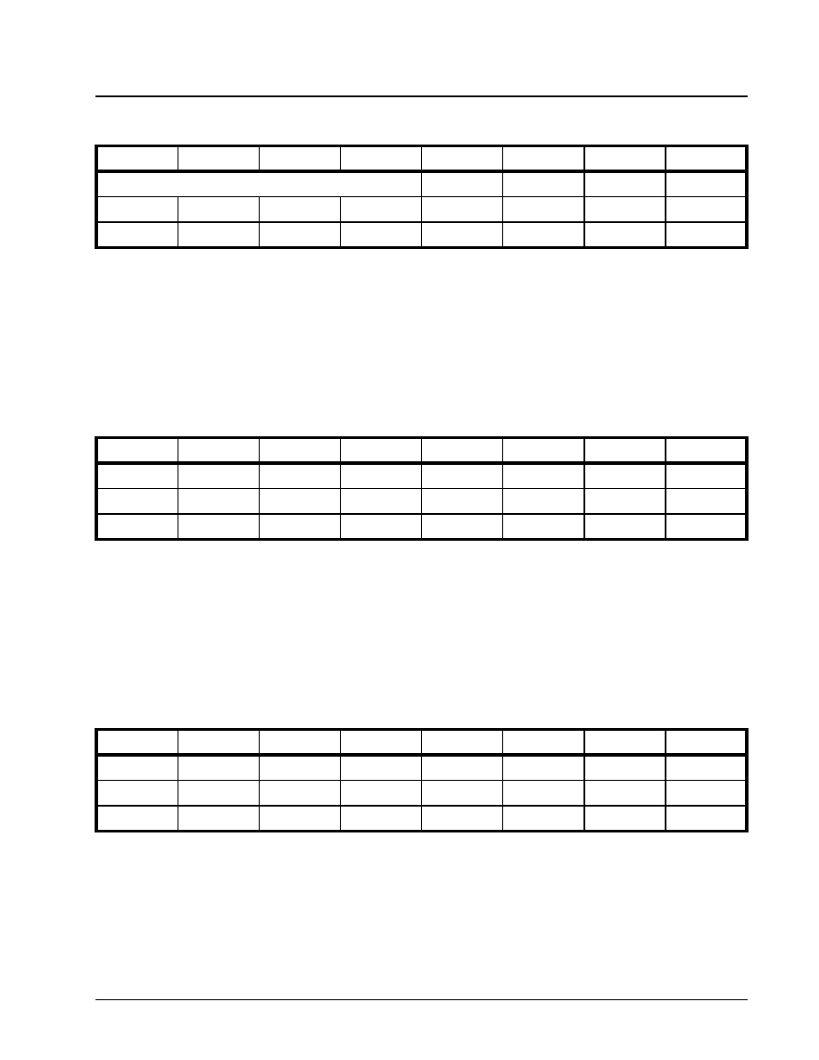
·Á
·Á
·Á
·Á
DS3/E3 FRAMER IC
XRT7250
REV. 1.1.1
89
Bits 3 - 0 F-Bit Mask[27:24]
These Read/Write bit-fields permit the user to insert
errors into the first four F-bits of a DS3 M-frame, for
test and diagnostic purposes. The Transmit DS3
Framer block automatically performs an XOR opera-
tion on the actual contents of these F-bit fields to
these register bit-fields. Therefore, for every "1" that
exists in these bit-fields, this will result in a change of
state for the corresponding F-bit, prior to being trans-
mitted to the Far-End Receive DS3 Framer.
If the Transmit DS3 Framer is to be operated in the
normal mode (e.g., when no errors are being injected
into these F-bit fields of the outbound DS3 frames),
then all of these bit-fields must be "0's".
2.3.5.8
Transmit DS3 F-Bit Mask Register - 2
(DS3 Applications)
Bits 7 - 0 F-Bit Mask[23:16]
These Read/Write bit-fields permit the user to insert
errors into the fifth through twelfth F-bits of a DS3 M-
frame, for test and diagnostic purposes. The Trans-
mit DS3 Framer block automatically performs an XOR
operation on the actual contents of these F-bit fields
to these register bit-fields. Therefore, for every "1"
that exists in these bit-fields, this will result in a
change of state for the corresponding F-bit, prior to
being transmitted to the Remote Terminal Equipment.
If the Transmit DS3 Framer block is to be operated in
the normal mode (e.g., when no errors are being in-
jected into these F-bit fields of the outbound DS3
frames), then all of these bit-fields must be "0's".
2.3.5.9
Transmit F-Bit Mask Register - 3 (DS3
Applications)
Bits 7 - 0 F-Bit Mask[15:8]
These Read/Write bit-fields permit the user to insert
errors into the thirteenth through twentieth F-bits of a
DS3 M-frame, for test and diagnostic purposes. The
Transmit DS3 Framer block automatically performs an
XOR operation on the actual contents of these F-bit
fields to these register bit-fields. Therefore, for every
"1" that exists in these bit-fields, this will result in a
change of state for the corresponding F-bit, prior to
being transmitted to the Remote Terminal Equipment.
If the Transmit DS3 Framer block is to be operated in
the normal mode (e.g., when no errors are being in-
jected into these F-bit fields of the outbound DS3
frames), then all of these bit-fields must be "0's".
2.3.5.10 Transmit F-Bit Mask Register - 4 (DS3
Applications)
TXDS3 F-BIT MASK REGISTER - 1 (ADDRESS = 0X36)
B
IT
7
B
IT
6
B
IT
5
B
IT
4
B
IT
3
B
IT
2
B
IT
1
B
IT
0
Not Used
FBit Mask[27] FBit Mask[26] FBit Mask[25] FBit Mask[24]
RO
RO
RO
RO
R/W
R/W
R/W
R/W
0
0
0
0
0
0
0
0
TXDS3 F-BIT MASK REGISTER - 2 (ADDRESS = 0X37)
B
IT
7
B
IT
6
B
IT
5
B
IT
4
B
IT
3
B
IT
2
B
IT
1
B
IT
0
FBit Mask[23] FBit Mask[22] FBit Mask[21] FBit Mask[20] FBit Mask[19] FBit Mask[18] FBit Mask[17] FBit Mask[16]
R/W
R/W
R/W
R/W
R/W
R/W
R/W
R/W
0
0
0
0
0
0
0
0
TXDS3 F-BIT MASK REGISTER - 3 (ADDRESS = 0X38)
B
IT
7
B
IT
6
B
IT
5
B
IT
4
B
IT
3
B
IT
2
B
IT
1
B
IT
0
FBit Mask[15] FBit Mask[14] FBit Mask[13] FBit Mask[12] FBit Mask[11] FBit Mask[10]
FBit Mask[9]
FBit Mask[8]
R/W
R/W
R/W
R/W
R/W
R/W
R/W
R/W
0
0
0
0
0
0
0
0

XRT7250
DS3/E3 FRAMER IC
·Á
·Á
·Á
·Á
REV. 1.1.1
90
Bits 7 - 0 F-Bit Mask[7:0]
These Read/Write bit-fields allow the user to insert
errors into the last eight F-bits of a DS3 M-frame, for
test and diagnostic purposes. The Transmit DS3
Framer block automatically performs an XOR opera-
tion on the actual contents of these F-bit fields to
these register bit-fields. Therefore, for every "1" that
exists in these bit-fields, this will result in a change of
state for the corresponding F-bit, prior to being trans-
mitted to the Remote Terminal Equipment.
If the Transmit DS3 Framer block is to be operated in
the normal mode (e.g., when no errors are being in-
jected into these F-bit fields of the outbound DS3
frames), then all of these bit-fields must be "0's".
2.3.6
Transmit E3 (ITU-T G.832) Configuration
Registers
2.3.6.1
Transmit E3 Configuration Register
(E3, ITU-T G.832)
Bit 4 - DLinNR
This Read/Write bit-field allows the user to specify
whether the LAPD Transmitter should insert the out-
bound LAPD Message frame octets into the NR byte-
field, or in the GC-byte-field, within each outbound E3
frame.
Writing a "1" configures the LAPD Transmitter to in-
sert the octets of the outbound LAPD Message frame
into the NR byte-field, within each outbound E3
frame. Writing in "0" configures the LAPD Transmitter
to insert the octets of the outbound LAPD Message
frame into the GC byte-field, within each outbound E3
frame.
Bit 2 - TxAIS Enable
This Read/Write bit-field allows the user to command
the Transmit E3 Framer to transmit an AIS pattern,
upon demand.
Writing a "0" to this bit-field allows the Transmit E3
Framer to transmit internally generated data (e.g., the
ITU-T G.832 compatible E3 frames with the E3 pay-
load data) to the Remote Terminal. Writing a "1" to
this bit-field causes the Transmit E3 Framer to trans-
mit an all "1's" pattern to the Remote Terminal.
N
OTE
: If the Transmit E3 Framer is transmitting an AIS pat-
tern to the Remote Terminal, then it is not transmitting any
E3 frames or ATM cell data. Consequently, if this command
is invoked, the Remote Terminal will experience an OOF
(Out of Frame) condition.
Bit 1 - TxLOS Enable
This Read/Write bit-field allows the user to command
the Transmit E3 Framer to transmit an LOS pattern,
upon demand.
Writing a "0" to this bit-field allows the Transmit E3
Framer to transmit internally generated data (e.g., the
ITU-T G.832 compatible E3 frames with ATM cell da-
ta) to the Remote Terminal. Writing a "1" to this bit-
field causes the Transmit E3 Framer to transmit an
"All 0's" pattern to the Remote Terminal.
N
OTE
: If the Transmit E3 Framer is transmitting an LOS
pattern to the Far-End Terminal, then it is not transmitting
any E3 frames or ATM cell data. Consequently, the Far-End
Terminal will experience an LOS (Loss of Signal) and OOF
(Out of Frame) condition.
Bit 0 - MARx (FERF and FEBE bit-field Loopback)
This Read/Write bit-field allows the user to specify
whether the value of the FERF and FEBE bit-fields, in
the outbound E3 frames, should be based upon Re-
TXDS3 F-BIT MASK REGISTER - 4 (ADDRESS = 0X39)
B
IT
7
B
IT
6
B
IT
5
B
IT
4
B
IT
3
B
IT
2
B
IT
1
B
IT
0
FBit Mask[7]
FBit Mask[6]
FBit Mask[5]
FBit Mask[4]
FBit Mask[3]
FBit Mask[2]
FBit Mask[1]
FBit Mask[0]
R/W
R/W
R/W
R/W
R/W
R/W
R/W
R/W
0
0
0
0
0
0
0
0
TXE3 CONFIGURATION REGISTER (ADDRESS = 0X30)
B
IT
7
B
IT
6
B
IT
5
B
IT
4
B
IT
3
B
IT
2
B
IT
1
B
IT
0
Not Used
TxDL
in NR
Not Used
TxAIS
Enable
TxLOS
Enable
TxMARx
RO
RO
RO
R/W
RO
R/W
R/W
R/W
0
0
0
0
0
0
0
0

·Á
·Á
·Á
·Á
DS3/E3 FRAMER IC
XRT7250
REV. 1.1.1
91
ceive E3 Framer conditions or upon the content of the
Tx MA Byte register (Address = 0x2A).
FERF and FEBE values are based upon Receive E3
Framer Conditions
If the user selects Receive E3 Framer conditions,
then the Transmit E3 Framer will set and clear the
FERF and FEBE bit-fields in response to the following
conditions.
a. FERF Bit-field
If the Receive E3 Framer (on the same UNI chip) is
currently experiencing an LOS, AIS, or LOF condi-
tion, then the Transmit E3 Framer will set the FERF
bit-field (in the outbound E3 frame) to "1". Converse-
ly, if the Receive E3 Framer is not experiencing any of
these conditions, then the Transmit E3 Framer will set
the FERF bit-field (in the outbound E3 frame) to "0".
b. FEBE bit-field
If the Receive E3 Framer detects a BIP-8 error in the
incoming E3 frame, then the Transmit E3 Framer will
set the FEBE bit-field (in the outbound E3 frame) to
"1". Conversely, if the Receive E3 Framer does not
detect a BIP-8 error in the incoming E3 frame, then
the Transmit E3 Framer will set the FEBE bit-field (in
the E3 outbound E3 frame) to "0".
FEBE and FERF values are based upon the contents
of the Tx MA Byte register
If the user selects the contents of the Tx MA Byte reg-
ister, then whatever value has been written into bit 7
(FERF), within the Tx MA Byte register (Address =
2Ah), will be the value of the FERF bit-field, in the
outbound E3 frame. Likewise, whatever value has
been written into Bit 6 (FEBE) within the Tx MA Byte
register, will be the value of the FEBE bit-field, in the
outbound E3 frame.
Writing a "1" into Bit 0 (MAx) within the Tx E3 Config-
uration register configures the Transmit E3 Framer to
set the FERF and FEBE bit-fields (in the outbound E3
frames) to values based upon Receive E3 Framer
conditions. Writing a "0" into this bit-field configures
the Transmit E3 Framer to set the FEBE and FEBE
bit-fields (in the outbound E3 frames) to the values
written into bit-fields 6 and 7 within the Tx MA Byte
register.
2.3.6.2
Transmit E3 LAPD Configuration Reg-
ister (E3, ITU-T G.832)
Bit 3 - Auto Retransmit
This Read/Write bit-field allows the user to configure
the LAPD Transmitter to either transmit the LAPD
Message frame only once, or repeatedly at one-sec-
ond intervals.
Writing a "0" to this bit-field configures the LAPD
Transmitter to transmit the LAPD Message frame
once. Afterwards, the LAPD Transmitter will halt
transmission, until it has commanded to transmit an-
other LAPD Message frame.
Writing a "1" to this bit-field configures the LAPD
Transmitter to transmit the LAPD Message frame re-
peatedly at One-Second intervals. In this configura-
tion, the LAPD Transmitter will repeat its transmission
of the LAPD Message frame until it has been dis-
abled.
Bit 1 - TxLAPD Message Length Select
This Read/Write bit-field permits the user to select
the length of the outbound LAPD Message frame.
Setting this bit-field to "0" configures the outbound
LAPD Message frame to be 76 bytes in length. Set-
ting this bit-field to "1" configures the outbound LAPD
Message frame to be 82 bytes in length.
Bit 0 - TxLAPD Enable
This Read/Write bit-field allows the user to enable or
disable the LAPD Transmitter. The LAPD Transmitter
must be enabled before it can be commanded to
transmit a LAPD Message frame (containing a PMDL
message) via the outbound DS3 frames, to the Far-
End Terminal.
Writing a "0" disables the LAPD Transmitter (default
condition). Writing a "1" enables the LAPD Transmit-
ter.
N
OTE
: For information on the LAPD Transmitter, please see
Section 3.2.3.2.
TXE3 LAPD CONFIGURATION REGISTER (ADDRESS = 0X33)
B
IT
7
B
IT
6
B
IT
5
B
IT
4
B
IT
3
B
IT
2
B
IT
1
B
IT
0
Not Used
Auto
Retransmit
Not Used
TxLAPD
Msg Length
TxLAPD
Enable
RO
RO
RO
RO
R/W
RO
R/W
R/W
0
0
0
0
1
0
0
0
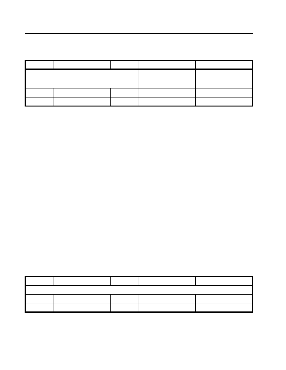
XRT7250
DS3/E3 FRAMER IC
·Á
·Á
·Á
·Á
REV. 1.1.1
92
2.3.6.3
Transmit E3 LAPD Status and Interrupt
Register (E3, ITU-T G.832)
Bit 3 - TxDL Start
This Read/Write bit-field allows the user to command
the LAPD Transmitter to do the following.
∑ Scan through the PMDL Message, within the Trans-
mit LAPD Message buffer, and search for a string of
five (5) consecutive "1's". The LAPD Transmitter
will then insert (or stuff) a "0" into the PMDL Mes-
sage data, immediately following any string of 5
consecutive "1's".
∑ Read in this stuffed PMDL Message from the Trans-
mit LAPD Message buffer, and encapsulate it into a
LAPD Message frame.
∑ Fragment the resulting LAPD Message frame into
octets.
∑ Insert these octets into either the GC byte-field or
the NR byte-field (depending upon the user's selec-
tion) in each outbound E3 frame.
A "0" to "1" transition, in this bit-field commands the
LAPD Transmitter to initiate the above-mentioned
procedure.
N
OTE
: Once the user has commanded the LAPD Transmit-
ter to start transmission, the LAPD Transmitter will repeat
the above-mentioned process once each second and will
insert flag sequence octets into the outbound LAPD chan-
nel, during the idle periods between transmissions.
Bit 2 - TxDL Busy
This Read-Only bit-field allows the user to poll or
monitor the status of the LAPD Transmitter to see if it
has completed its transmission of the LAPD Message
frame. The LAPD Transmitter will set this bit-field to
"1", while it is in the process of transmitting the LAPD
Message frame. However, the LAPD Transmitter will
clear this bit-field to "0" once it has completed its
transmission of the LAPD Message frame.
Bit 1 - TxLAPD Interrupt Enable
This Read/Write bit-field allows the user to enable or
disable the LAPD Message frame Transmission Com-
plete interrupt.
Writing a "0" to this bit-field disables this interrupt.
Writing a "1" to this bit-field enables this interrupt.
Bit 0 - TxLAPD Interrupt Status
This Reset-upon-Read bit-field allows the user to de-
termine if the LAPD Message Frame Transmission
Complete interrupt has occurred since the last read of
this register. If this bit-field contains a "1" then the
LAPD Message Frame Transmission Complete inter-
rupt has occurred since the last read of this register.
Conversely, if this bit-field contains a "0" then it has
not.
2.3.6.4
Transmit E3 GC Byte Register (E3, ITU-
T G.832)
This Read/Write byte-field allows the user to specify
the contents of the GC byte-field in each outbound E3
frame.
N
OTE
: The contents of this register is ignored, if the LAPD
Transmitter is enabled and has been configured to insert
the comprising octets of an outbound LAPD Message
frame into the GC byte-field of each outbound E3 frame
(e.g., if DLinNR = "0").
2.3.6.5
Transmit E3 MA Byte Register (E3, ITU-
T G.832)
TXE3 LAPD STATUS AND INTERRUPT REGISTER (ADDRESS = 0X34)
B
IT
7
B
IT
6
B
IT
5
B
IT
4
B
IT
3
B
IT
2
B
IT
1
B
IT
0
Not Used
TxDL Start
TxDL Busy
TxLAPD
Interrupt
Enable
TxLAPD
Interrupt
Status
RO
RO
RO
RO
R/W
RO
R/W
RUR
0
0
0
0
0
0
0
0
TXE3 GC BYTE REGISTER (ADDRESS = 0X35)
B
IT
7
B
IT
6
B
IT
5
B
IT
4
B
IT
3
B
IT
2
B
IT
1
B
IT
0
TxGC[7:0]
R/W
R/W
R/W
R/W
R/W
R/W
R/W
R/W
0
0
0
0
0
0
0
0
·Á
·Á
·Á
·Á
DS3/E3 FRAMER IC
XRT7250
REV. 1.1.1
93
This Read/Write byte-fields allows the user to specify
the contents of the MA byte-field in each outbound E3
frame.
N
OTE
: The values written into bit-fields 6 (FEBE) and 7
(FERF) are inserted into outbound E3 frames, only if bit-
field 0 (MAx) within the Tx E3 Configuration Register
(Address = 28h) is set to "0". Otherwise, the Transmit E3
Framer will set the FERF and FEBE values, within each
outbound E3 frame, to values based upon Receive E3
Framer conditions.
2.3.6.6
Transmit E3 NR Byte Register (E3, ITU-
T G.832)
This Read/Write byte-field allows the user to specify
the contents of the NR byte-field in each outbound E3
frame.
N
OTE
: The contents of this register is ignored, if the LAPD
Transmitter is enabled and has been configured to insert
the comprising octets of an outbound LAPD Message
frame into the NR byte-field of each outbound E3 frame
(e.g., if DLinNR = "1").
2.3.6.7
Transmit E3 TTB-0 Register (E3, ITU-T
G.832)
This Read/Write byte-field, along with the Tx TTB-1
through Tx TTB-15 registers allows a user to define a
Trail Access Point Identifier sequence of bytes, that
will be transmitted to the Far-End Terminal. The Far-
End Receiving Terminal will use this sequence of
bytes to verify that it is connected to the proper Trans-
mitting Terminal. The Transmit E3 Framer will take
the contents of these 16 registers, and insert them in-
to the TR byte of the outbound E3 frame. In the first
of a set of 16 E3 Frames, the Transmit E3 Framer will
read in the contents of this register, and insert it into
the TR byte-field, within the very next outbound E3
frame.
This particular byte-field should contain the pattern
"[1, C6, C5, C4, C3, C2, C1, C0]" where C6 through
C0 are the results of a CRC-7 calculation over the
previous 16-byte frame.
N
OTE
: The XRT7250 Framer IC will not compute this CRC-
7 value. It is up to the user's hardware and/or software to
compute this value, prior to writing it into this register.
2.3.6.8
Transmit E3 TTB-1 Register (E3, ITU-T
G.832)
TXE3 MA BYTE REGISTER (ADDRESS = 0X36)
B
IT
7
B
IT
6
B
IT
5
B
IT
4
B
IT
3
B
IT
2
B
IT
1
B
IT
0
Transmit MA Byte
FERF
FEBE
Payload Type
Payload Dependent
Timing
Marker
R/W
R/W
R/W
R/W
R/W
R/W
R/W
R/W
0
0
0
1
0
0
0
0
TXE3 NR BYTE REGISTER (ADDRESS = 0X37)
B
IT
7
B
IT
6
B
IT
5
B
IT
4
B
IT
3
B
IT
2
B
IT
1
B
IT
0
TxNR[7:0]
R/W
R/W
R/W
R/W
R/W
R/W
R/W
R/W
0
0
0
1
0
0
0
0
TXE3 TTB-0 REGISTER (ADDRESS = 0X38)
B
IT
7
B
IT
6
B
IT
5
B
IT
4
B
IT
3
B
IT
2
B
IT
1
B
IT
0
TxTTB0[7:0]
R/W
R/W
R/W
R/W
R/W
R/W
R/W
R/W
1
0
0
1
0
0
0
0
XRT7250
DS3/E3 FRAMER IC
·Á
·Á
·Á
·Á
REV. 1.1.1
94
This Read/Write byte-field, along with the TxTTB-0
and TxTTB-2 through TxTTB-15 register allows a us-
er to define a Trail Access Point Identifier sequence of
bytes, that will be transmitted to the Far-End Termi-
nal. The Far-End Receiving Terminal will use this se-
quence of bytes to verify that it is connected to the
proper Transmitting Terminal. The Transmit E3 Fram-
er will take the contents of these 16 registers, and in-
sert them into the TR byte of the outbound E3 frame.
In the second of a set of 16 E3 Frames, the Transmit
E3 Framer will read in the contents of this register,
and insert it into the TR byte-field, within the very next
outbound E3 frame.
The contents of this register, along with Tx TTB-2
through Tx TTB-15 are used to transmit 15 ASCII
characters required for the E.164 numbering format.
2.3.6.9
Transmit E3 TTB-2 Register (E3, ITU-T
G.832)
This Read/Write byte-field, along with the TxTTB-0,
TxTTB-1 and TxTTB-3 through TxTTB-15 register al-
lows a user to define a Trail Access Point Identifier se-
quence of bytes, that will be transmitted to the Far-
End Terminal. The Far-End Receiving Terminal will
use this sequence of bytes to verify that it is connect-
ed to the proper Transmitting Terminal. The Transmit
E3 Framer will take the contents of these 16 registers,
and insert them into the TR byte of the outbound E3
frame. In the third of a set of 16 E3 Frames, the
Transmit E3 Framer will read in the contents of this
register, and insert it into the TR byte-field, within the
very next outbound E3 frame.
The contents of this register, along with Tx TTB-1,
and Tx TTB-3 through Tx TTB-15 are used to trans-
mit 15 ASCII characters required for the E.164 num-
bering format.
2.3.6.10 Transmit E3 TTB-3 Register (E3, ITU-T
G.832)
This Read/Write byte-field, along with the TxTTB-0
through TxTTB-2 and TxTTB-4 through TxTTB-15
registers allows a user to define a Trail Access Point
Identifier sequence of bytes, that will be transmitted to
the Far-End Terminal. The Far-End Receiving Termi-
nal will use this sequence of bytes to verify that it is
connected to the proper Transmitting Terminal. The
Transmit E3 Framer will take the contents of these 16
registers, and insert them into the TR byte of the out-
bound E3 frame. In the fourth of a set of 16 E3
Frames, the Transmit E3 Framer will read in the con-
tents of this register, and insert it into the TR byte-
field, within the very next outbound E3 frame.
TXE3 TTB-1 REGISTER (ADDRESS = 0X39)
B
IT
7
B
IT
6
B
IT
5
B
IT
4
B
IT
3
B
IT
2
B
IT
1
B
IT
0
TxTTB-1[7:0]
R/W
R/W
R/W
R/W
R/W
R/W
R/W
R/W
0
0
0
0
0
0
0
0
TXE3 TTB-2 REGISTER (ADDRESS = 0X3A)
B
IT
7
B
IT
6
B
IT
5
B
IT
4
B
IT
3
B
IT
2
B
IT
1
B
IT
0
TxTTB-2[7:0]
R/W
R/W
R/W
R/W
R/W
R/W
R/W
R/W
0
0
0
0
0
0
0
0
TXE3 TTB-3 REGISTER (ADDRESS = 0X3B)
B
IT
7
B
IT
6
B
IT
5
B
IT
4
B
IT
3
B
IT
2
B
IT
1
B
IT
0
TxTTB-3[7:0]
R/W
R/W
R/W
R/W
R/W
R/W
R/W
R/W
0
0
0
0
0
0
0
0
·Á
·Á
·Á
·Á
DS3/E3 FRAMER IC
XRT7250
REV. 1.1.1
95
The contents of this register, along with Tx TTB-1, Tx
TTB-2 and Tx TTB-4 through Tx TTB-15 are used to
transmit 15 ASCII characters required for the E.164
numbering format.
2.3.6.11 Transmit E3 TTB-4 Register (E3, ITU-T
G.832)
This Read/Write byte-field, along with the TxTTB-0
through TxTTB-3 and TxTTB-5 through TxTTB-15
registers allows a user to define a Trail Access Point
Identifier sequence of bytes, that will be transmitted to
the Far-End Terminal. The Far-End Receiving Termi-
nal will use this sequence of bytes to verify that it is
connected to the proper Transmitting Terminal. The
Transmit E3 Framer will take the contents of these 16
registers, and insert them into the TR byte of the out-
bound E3 frame. In the fifth of a set of 16 E3 Frames,
the Transmit E3 Framer will read in the contents of
this register, and insert it into the TR byte-field, within
the very next outbound E3 frame.
The contents of this register, along with Tx TTB-1
through Tx TTB-3 and Tx TTB-5 through Tx TTB-15
are used to transmit 15 ASCII characters required for
the E.164 numbering format.
2.3.6.12 Transmit E3 TTB-5 Register (E3, ITU-T
G.832)
This Read/Write byte-field, along with the Tx TTB-0
through Tx TTB-4 and Tx TTB-6 through Tx TTB-15
registers allows a user to define a Trail Access Point
Identifier sequence of bytes, that will be transmitted to
the Far-End Terminal. The Far-End Receiving Termi-
nal will use this sequence of bytes to verify that it is
connected to the proper Transmitting Terminal. The
Transmit E3 Framer will take the contents of these 16
registers, and insert them into the TR byte of the out-
bound E3 frame. In the sixth of a set of 16 E3
Frames, the Transmit E3 Framer will read in the con-
tents of this register, and insert it into the TR byte-
field, within the very next outbound E3 frame.
The contents of this register, along with Tx TTB-1
through Tx TTB-4 and Tx TTB-6 through Tx TTB-15
are used to transmit 15 ASCII characters required for
the E.164 numbering format.
2.3.6.13 Transmit E3 TTB-6 Register (E3, ITU-T
G.832)
This Read/Write byte-field, along with the Tx TTB-0
through Tx TTB-5 and Tx TTB-7 through Tx TTB-15
registers allows a user to define a Trail Access Point
Identifier sequence of bytes, that will be transmitted to
the Far-End Terminal. The Far-End Receiving Termi-
nal will use this sequence of bytes to verify that it is
TXE3 TTB-4 REGISTER (ADDRESS = 0X3C)
B
IT
7
B
IT
6
B
IT
5
B
IT
4
B
IT
3
B
IT
2
B
IT
1
B
IT
0
TxTTB-4[7:0]
R/W
R/W
R/W
R/W
R/W
R/W
R/W
R/W
0
0
0
0
0
0
0
0
TXE3 TTB-5 REGISTER (ADDRESS = 0X3D)
B
IT
7
B
IT
6
B
IT
5
B
IT
4
B
IT
3
B
IT
2
B
IT
1
B
IT
0
TxTTB-5[7:0]
R/W
R/W
R/W
R/W
R/W
R/W
R/W
R/W
0
0
0
0
0
0
0
0
TXE3 TTB-6 REGISTER (ADDRESS = 0X3E)
B
IT
7
B
IT
6
B
IT
5
B
IT
4
B
IT
3
B
IT
2
B
IT
1
B
IT
0
TxTTB-6[7:0]
R/W
R/W
R/W
R/W
R/W
R/W
R/W
R/W
0
0
0
0
0
0
0
0
XRT7250
DS3/E3 FRAMER IC
·Á
·Á
·Á
·Á
REV. 1.1.1
96
connected to the proper Transmitting Terminal. The
Transmit E3 Framer will take the contents of these 16
registers, and insert them into the TR byte of the out-
bound E3 frame. In the seventh of a set of 16 E3
Frames, the Transmit E3 Framer will read in the con-
tents of this register, and insert it into the TR byte-
field, within the very next outbound E3 frame.
The contents of this register, along with Tx TTB-1
through Tx TTB-5 and Tx TTB-7 through Tx TTB-15
are used to transmit 15 ASCII characters required for
the E.164 numbering format.
2.3.6.14 Transmit E3 TTB-7 Register (E3, ITU-T
G.832)
This Read/Write byte-field, along with the Tx TTB-0
through Tx TTB-6 and Tx TTB-8 through Tx TTB-15
registers allows a user to define a Trail Access Point
Identifier sequence of bytes, that will be transmitted to
the Far-End Terminal. The Far-End Receiving Termi-
nal will use this sequence of bytes to verify that it is
connected to the proper Transmitting Terminal. The
Transmit E3 Framer will take the contents of these 16
registers, and insert them into the TR byte of the out-
bound E3 frame. In the eighth of a set of 16 E3
Frames, the Transmit E3 Framer will read in the con-
tents of this register, and insert it into the TR byte-
field, within the very next outbound E3 frame.
The contents of this register, along with Tx TTB-1
through Tx TTB-6 and Tx TTB-8 through Tx TTB-15
are used to transmit 15 ASCII characters required for
the E.164 numbering format.
2.3.6.15 Transmit E3 TTB-8 Register (E3, ITU-T
G.832)
This Read/Write byte-field, along with the Tx TTB-0
through Tx TTB-7 and Tx TTB-9 through Tx TTB-15
registers allows a user to define a Trail Access Point
Identifier sequence of bytes, that will be transmitted to
the Far-End Terminal. The Far-End Receiving Termi-
nal will use this sequence of bytes to verify that it is
connected to the proper Transmitting Terminal. The
Transmit E3 Framer will take the contents of these 16
registers, and insert them into the TR byte of the out-
bound E3 frame. In the ninth of a set of 16 E3
Frames, the Transmit E3 Framer will read in the con-
tents of this register, and insert it into the TR byte-
field, within the very next outbound E3 frame.
The contents of this register, along with Tx TTB-1
through Tx TTB-7 and Tx TTB-9 through Tx TTB-15
are used to transmit 15 ASCII characters required for
the E.164 numbering format.
2.3.6.16 Transmit E3 TTB-9 Register (E3, ITU-T
G.832)
TXE3 TTB-7 REGISTER (ADDRESS = 0X3F)
B
IT
7
B
IT
6
B
IT
5
B
IT
4
B
IT
3
B
IT
2
B
IT
1
B
IT
0
TxTTB-7[7:0]
R/W
R/W
R/W
R/W
R/W
R/W
R/W
R/W
0
0
0
0
0
0
0
0
TXE3 TTB-8 REGISTER (ADDRESS = 0X40)
B
IT
7
B
IT
6
B
IT
5
B
IT
4
B
IT
3
B
IT
2
B
IT
1
B
IT
0
TxTTB-8[7:0]
R/W
R/W
R/W
R/W
R/W
R/W
R/W
R/W
0
0
0
0
0
0
0
0
TXE3 TTB-9 REGISTER (ADDRESS = 0X41)
B
IT
7
B
IT
6
B
IT
5
B
IT
4
B
IT
3
B
IT
2
B
IT
1
B
IT
0
TxTTB-9[7:0]
R/W
R/W
R/W
R/W
R/W
R/W
R/W
R/W
0
0
0
0
0
0
0
0

·Á
·Á
·Á
·Á
DS3/E3 FRAMER IC
XRT7250
REV. 1.1.1
97
This Read/Write byte-field, along with the Tx TTB-0
through Tx TTB-8 and Tx TTB-10 through Tx TTB-15
registers allows a user to define a Trail Access Point
Identifier sequence of bytes, that will be transmitted to
the Far-End Terminal. The Far-End Receiving Termi-
nal will use this sequence of bytes to verify that it is
connected to the proper Transmitting Terminal. The
Transmit E3 Framer will take the contents of these 16
registers, and insert them into the TR byte of the out-
bound E3 frame. In the tenth of a set of 16 E3
Frames, the Transmit E3 Framer will read in the con-
tents of this register, and insert it into the TR byte-
field, within the very next outbound E3 frame.
The contents of this register, along with Tx TTB-1
through Tx TTB-8 and Tx TTB-10 through Tx TTB-15
are used to transmit 15 ASCII characters required for
the E.164 numbering format.
2.3.6.17 Transmit E3 TTB-10 Register (E3, ITU-T
G.832)
This Read/Write byte-field, along with the Tx TTB-0
through Tx TTB-9 and Tx TTB-11 through Tx TTB-15
registers allows a user to define a Trail Access Point
Identifier sequence of bytes, that will be transmitted to
the Far-End Terminal. The Far-End Receiving Termi-
nal will use this sequence of bytes to verify that it is
connected to the proper Transmitting Terminal. The
Transmit E3 Framer will take the contents of these 16
registers, and insert them into the TR byte of the out-
bound E3 frame. In the eleventh of a set of 16 E3
Frames, the Transmit E3 Framer will read in the con-
tents of this register, and insert it into the TR byte-
field, within the very next outbound E3 frame.
The contents of this register, along with Tx TTB-1
through Tx TTB-9 and Tx TTB-11 through Tx TTB-15
are used to transmit 15 ASCII characters required for
the E.164 numbering format.
2.3.6.18 Transmit E3 TTB-11 Register (E3, ITU-T
G.832)
This Read/Write byte-field, along with the Tx TTB-0
through Tx TTB-10 and Tx TTB-12 through Tx TTB-
15 registers allows a user to define a Trail Access
Point Identifier sequence of bytes, that will be trans-
mitted to the Far-End Terminal. The Far-End Receiv-
ing Terminal will use this sequence of bytes to verify
that it is connected to the proper Transmitting Termi-
nal. The Transmit E3 Framer will take the contents of
these 16 registers, and insert them into the TR byte of
the outbound E3 frame. In the twelfth of a set of 16
E3 Frames, the Transmit E3 Framer will read in the
contents of this register, and insert it into the TR byte-
field, within the very next outbound E3 frame.
The contents of this register, along with Tx TTB-1
through Tx TTB-10 and Tx TTB-12 through Tx TTB-
15 are used to transmit 15 ASCII characters required
for the E.164 numbering format.
2.3.6.19 3.3.2.77 Transmit E3 TTB-12 Register
(E3, ITU-T G.832)
TXE3 TTB-10 REGISTER (ADDRESS = 0X42)
B
IT
7
B
IT
6
B
IT
5
B
IT
4
B
IT
3
B
IT
2
B
IT
1
B
IT
0
TxTTB-10[7:0]
R/W
R/W
R/W
R/W
R/W
R/W
R/W
R/W
0
0
0
0
0
0
0
0
TXE3 TTB-11 REGISTER (ADDRESS = 0X43)
B
IT
7
B
IT
6
B
IT
5
B
IT
4
B
IT
3
B
IT
2
B
IT
1
B
IT
0
TxTTB-11[7:0]
R/W
R/W
R/W
R/W
R/W
R/W
R/W
R/W
0
0
0
0
0
0
0
0

XRT7250
DS3/E3 FRAMER IC
·Á
·Á
·Á
·Á
REV. 1.1.1
98
This Read/Write byte-field, along with the Tx TTB-0
through Tx TTB-11 and Tx TTB-13 through Tx TTB-
15 registers allows a user to define a Trail Access
Point Identifier sequence of bytes, that will be trans-
mitted to the Far-End Terminal. The Far-End Receiv-
ing Terminal will use this sequence of bytes to verify
that it is connected to the proper Transmitting Termi-
nal. The Transmit E3 Framer will take the contents of
these 16 registers, and insert them into the TR byte of
the outbound E3 frame. In the thirteenth of a set of
16 E3 Frames, the Transmit E3 Framer will read in the
contents of this register, and insert it into the TR byte-
field, within the very next outbound E3 frame.
The contents of this register, along with Tx TTB-1
through Tx TTB-11 and Tx TTB-13 through Tx TTB-
15 are used to transmit 15 ASCII characters required
for the E.164 numbering format.
2.3.6.20 Transmit E3 TTB-13 Register (E3, ITU-T
G.832)
This Read/Write byte-field, along with the Tx TTB-0
through Tx TTB-12, Tx-TTB-14, and Tx TTB-15 regis-
ters allows a user to define a Trail Access Point Iden-
tifier sequence of bytes, that will be transmitted to the
Far-End Terminal. The Far-End Receiving Terminal
will use this sequence of bytes to verify that it is con-
nected to the proper Transmitting Terminal. The
Transmit E3 Framer will take the contents of these 16
registers, and insert them into the TR byte of the out-
bound E3 frame. In the fourteenth of a set of 16 E3
Frames, the Transmit E3 Framer will read in the con-
tents of this register, and insert it into the TR byte-
field, within the very next outbound E3 frame.
The contents of this register, along with Tx TTB-1
through Tx TTB-12, Tx TTB-14 and Tx TTB-15 are
used to transmit 15 ASCII characters required for the
E.164 numbering format.
2.3.6.21 Transmit E3 TTB-14 Register (E3, ITU-T
G.832)
This Read/Write byte-field, along with the Tx TTB-0
through Tx TTB-13 and Tx TTB-15 registers allows a
user to define a Trail Access Point Identifier sequence
of bytes, that will be transmitted to the Far-End Termi-
nal. The Far-End Receiving Terminal will use this se-
quence of bytes to verify that it is connected to the
proper Transmitting Terminal. The Transmit E3 Fram-
er will take the contents of these 16 registers, and in-
sert them into the TR byte of the outbound E3 frame.
In the fifteenth of a set of 16 E3 Frames, the Transmit
E3 Framer will read in the contents of this register,
and insert it into the TR byte-field, within the very next
outbound E3 frame.
TXE3 TTB-12 REGISTER (ADDRESS = 0X44)
B
IT
7
B
IT
6
B
IT
5
B
IT
4
B
IT
3
B
IT
2
B
IT
1
B
IT
0
TxTTB-12[7:0]
R/W
R/W
R/W
R/W
R/W
R/W
R/W
R/W
0
0
0
0
0
0
0
0
TXE3 TTB-13 REGISTER (ADDRESS = 0X45)
B
IT
7
B
IT
6
B
IT
5
B
IT
4
B
IT
3
B
IT
2
B
IT
1
B
IT
0
TxTTB-13[7:0]
R/W
R/W
R/W
R/W
R/W
R/W
R/W
R/W
0
0
0
0
0
0
0
0
TXE3 TTB-14 REGISTER (ADDRESS = 0X46)
B
IT
7
B
IT
6
B
IT
5
B
IT
4
B
IT
3
B
IT
2
B
IT
1
B
IT
0
TxTTB-14[7:0]
R/W
R/W
R/W
R/W
R/W
R/W
R/W
R/W
0
0
0
0
0
0
0
0

·Á
·Á
·Á
·Á
DS3/E3 FRAMER IC
XRT7250
REV. 1.1.1
99
The contents of this register, along with Tx TTB-1
through Tx TTB-13 and Tx TTB-15 are used to trans-
mit 15 ASCII characters required for the E.164 num-
bering format.
2.3.6.22 Transmit E3 TTB-15 Register (E3, ITU-T
G.832)
This Read/Write byte-field, along with the Tx TTB-0
through Tx TTB-14 registers allows a user to define a
Trail Access Point Identifier sequence of bytes, that
will be transmitted to the Far-End Terminal. The Far-
End Receiving Terminal will use this sequence of
bytes to verify that it is connected to the proper Trans-
mitting Terminal. The Transmit E3 Framer will take
the contents of these 16 registers, and insert them in-
to the TR byte of the outbound E3 frame. In the six-
teenth of a set of 16 E3 Frames, the Transmit E3
Framer will read in the contents of this register, and
insert it into the TR byte-field, within the very next out-
bound E3 frame.
The contents of this register, along with Tx TTB-1
through Tx TTB-15 are used to transmit 15 ASCII
characters required for the E.164 numbering format.
2.3.6.23 Transmit E3 FA1 Byte Error Mask Reg-
ister (E3, ITU-T G.832)
This Read/Write bit-field allows the user to insert er-
rors into the Framing Alignment octet, FA1 of each
outbound E3 frame. The user may wish to do this for
equipment testing purposes. Prior to transmission,
the Transmit E3 Framer reads in the FA1 byte, and
performs an XOR operation with it and the contents of
this register. The results of this operation are written
back into the FA1 octet position, in each outbound E3
frame. Consequently, to insure errors are not injected
into the FA1 octet of the outbound E3 frames, the
contents of this register must be set to all "0's" (the
default value).
2.3.6.24 Transmit E3 FA2 Byte Error Mask Reg-
ister (E3, ITU-T G.832)
This Read/Write bit-field allows the user to insert er-
rors into the Framing Alignment octet, FA2 of each
outbound E3 frame. The user may wish to do this for
equipment testing purposes. Prior to transmission,
the Transmit E3 Framer reads in the FA2 byte, and
performs an XOR operation with it and the contents of
this register. The results of this operation are written
back into the FA2 octet position, in each outbound E3
frame. Consequently, to insure errors are not injected
into the FA2 octet of the outbound E3 frames, the
TXE3 TTB-15 REGISTER (ADDRESS = 0X47)
B
IT
7
B
IT
6
B
IT
5
B
IT
4
B
IT
3
B
IT
2
B
IT
1
B
IT
0
TxTTB-15[7:0]
R/W
R/W
R/W
R/W
R/W
R/W
R/W
R/W
0
0
0
0
0
0
0
0
TXE3 FA1 ERROR MASK REGISTER (ADDRESS = 0X48)
B
IT
7
B
IT
6
B
IT
5
B
IT
4
B
IT
3
B
IT
2
B
IT
1
B
IT
0
TxFA1_Error_Mask_Byte[7:0]
R/W
R/W
R/W
R/W
R/W
R/W
R/W
R/W
0
0
0
0
0
0
0
0
TXE3 FA2 ERROR MASK REGISTER (ADDRESS = 0X49)
B
IT
7
B
IT
6
B
IT
5
B
IT
4
B
IT
3
B
IT
2
B
IT
1
B
IT
0
TxFA2_Error_Mask_Byte[7:0]
R/W
R/W
R/W
R/W
R/W
R/W
R/W
R/W
0
0
0
0
0
0
0
0

XRT7250
DS3/E3 FRAMER IC
·Á
·Á
·Á
·Á
REV. 1.1.1
100
contents of this register must be set to all "0's" (the
default value).
2.3.6.25 Transmit E3 BIP-8 Error Mask Register
(E3, ITU-T G.832)
This Read/Write bit-field allows the user to insert er-
rors into EM (Error Monitor) octet of each outbound
E3 frame. The user may wish to do this for equip-
ment testing purposes. Prior to transmission, the
Transmit E3 Framer reads in the EM byte, and per-
forms an XOR operation with it and the contents of
this register. The results of this operation are written
back into the EM octet position, in each outbound E3
frame. Consequently, to insure errors are not injected
into the EM octet of the outbound E3 frames, the con-
tents of this register must be set to all "0's" (the de-
fault value).
2.3.7
Transmit E3 Framer Configuration Regis-
ters (ITU-T G.751)
2.3.7.1
Transmit E3 Configuration Register
(ITU-T G.751)
Bit 7 - TxBIP-4 Enable
This Read/Write bit-field permits the user to configure
the Transmit Section of the Framer IC, to compute an
insert the BIP-4 value into each outbound E3 frame.
Setting this bit-field to "0", configures the Transmit
Section of the Framer IC to NOT compute and insert
the BIP-4 value into each outbound E3 frame. In-
stead these four bits will contain data that has been
input via the Input Interface.
Setting this bit-field to "1", configures the Transmit
Section of the Framer IC to compute and insert the
BIP-4 value into each outbound E3 frame.
N
OTE
: For more information on these BIP-4 Calculations,
please see Section 4.2.4.2.2.
Bit 6, 5, TxASourceSel[1:0]
These two Read/Write bit-fields combine to specify
the source of the A-bit, within each outbound E3
frame. The relationship between these two bit-fields
and the resulting source of the A Bit is tabulated be-
low.
TXE3 BIP-8 ERROR MASK REGISTER (ADDRESS = 0X4A)
B
IT
7
B
IT
6
B
IT
5
B
IT
4
B
IT
3
B
IT
2
B
IT
1
B
IT
0
TxBIP-8_Error_Mask_Byte[7:0]
R/W
R/W
R/W
R/W
R/W
R/W
R/W
R/W
0
0
0
0
0
0
0
0
TXE3 CONFIGURATION REGISTER (ADDRESS = 0X30)
B
IT
7
B
IT
6
B
IT
5
B
IT
4
B
IT
3
B
IT
2
B
IT
1
B
IT
0
Tx
BIP-4
Enable
TxASourceSel[1:0]
TxNSourceSel[1:0]
Tx AIS
Enable
Tx LOS
Enable
Tx FAS
Source
Select
R/W
R/W
R/W
R/W
R/W
R/W
R/W
R/W
0
0
0
0
0
0
0
0
T
X
AS
OURCE
S
EL
[1:0]
S
OURCE
OF
A B
IT
00
TxE3 Service Bits Register (Address = 0x35)
01
Transmit Overhead Data Input Interface
10
Transmit Payload Data Input Interface

·Á
·Á
·Á
·Á
DS3/E3 FRAMER IC
XRT7250
REV. 1.1.1
101
N
OTE
: For more information on the A-bit, within the ITU-T
G.751 frame, please see Section 4.1.1.1.
Bits 4, 3, TxNSourceSel[1:0]
These two Read/Write bit-fields combine to specify
the source of the N-bit, within each outbound E3
frame. The relationship between these two bit-fields
and the resulting source of the N Bit is tabulated be-
low.
N
OTE
: For more information on the N-bit, within the ITU-T
G.751 frame, please see Section 4.1.1.2.
Bit 2 - TxAIS Enable
This Read/Write bit-field permits the user to configure
the Transmit Section of the Framer IC to transmit an
AIS pattern to the remote terminal
Setting this bit-field to "0" configures the Transmit
Section (of the chip) to transmit data in a normal man-
ner (e.g., as received via the Input Interface).
Setting this bit-field to "1" configures the Transmit
Section (of the chip) to transmit an "All Ones" pattern
(e.g., an AIS pattern) to the remote terminal.
N
OTE
: For more information on the AIS pattern, please see
Section 4.2.4.2.1.1.
Bit 1 - TxLOS Enable
This Read/Write bit-field permits the user to configure
the Transmit Section of the Framer IC to transmit an
LOS (e.g., All Zeros) pattern to the remote terminal
Setting this bit-field to "0" configures the Transmit
Section (of the chip) to transmit data in a normal man-
ner (e.g., as received via the Input Interface).
Setting this bit-field to "1" configures the Transmit
Section (of the chip) to transmit an "All Zeros" pattern
(e.g., an LOS pattern) to the remote terminal.
N
OTE
: For more information on the LOS pattern, please
see Section 4.2.4.2.1.2.
Bit 0 - TxFAS Source Select
This Read/Write bit-field permits the user to configure
the Transmit Section of the Framer IC to either:
a. Internally generate the FAS (Framing Alignment
Signal) pattern, within the outbound E3 frames,
or to
b. use the Input Interface as the source for the FAS
pattern.
Setting this bit-field to "0" configures the Transmit
Section of the Framer IC to internally generate the
FAS pattern, for each outbound E3 frame.
Setting this bit-field to "1" configures the Transmit
Section of the Framer IC to use the Input Interface as
the source for the FAS pattern.
N
OTE
: For more information on the FAS pattern, please see
Section 4.1.
2.3.7.2
Transmit E3 LAPD Configuration Reg-
ister (ITU-T G.751)
11
Functions as a FEBE (Far-End-Block Error) bit-field.
This bit-field is set to "0", if the Near-End Receive Section (within this chip) detects no BIP-4
Errors within the incoming E3 frames.
This bit-field is set to "1", if the Near-End Receive Section (within this chip) detects a BIP-4
Error within the incoming E3 frame.
T
X
AS
OURCE
S
EL
[1:0]
S
OURCE
OF
A B
IT
T
X
NS
OURCE
S
EL
[1:0]
S
OURCE
OF
N B
IT
00
TxE3 Service Bits Register (Address = 0x35)
01
Transmit Overhead Data Input Interface
10
Transmit LAPD Controller
11
Transmit Payload Data Input Interface
.

XRT7250
DS3/E3 FRAMER IC
·Á
·Á
·Á
·Á
REV. 1.1.1
102
Bit 3 - Auto Retransmit
This Read/Write bit-field allows the user to configure
the LAPD Transmitter to either transmit the LAPD
Message frame only once, or repeatedly at one-sec-
ond intervals.
Writing a "0" to this bit-field configures the LAPD
Transmitter to transmit the LAPD Message frame
once. Afterwards, the LAPD Transmitter will halt
transmission, until it has commanded to transmit an-
other LAPD Message frame.
Writing a "1" to this bit-field configures the LAPD
Transmitter to transmit the LAPD Message frame re-
peatedly at One-Second intervals. In this configura-
tion, the LAPD Transmitter will repeat its transmission
of the LAPD Message frame until it has been dis-
abled.
Bit 1 - TxLAPD Message Length Select
This Read/Write bit-field permits the user to select
the length of the outbound LAPD Message frame.
Setting this bit-field to "0" configures the outbound
LAPD Message frame to be 76 bytes in length. Set-
ting this bit-field to "1" configures the outbound LAPD
Message frame to be 82 bytes in length.
Bit 0 - TxLAPD Enable
This Read/Write bit-field allows the user to enable or
disable the LAPD Transmitter. The LAPD Transmitter
must be enabled before it can be commanded to
transmit a LAPD Message frame (containing a PMDL
message) via the outbound DS3 frames, to the Far-
End Terminal.
Writing a "0" disables the LAPD Transmitter (default
condition). Writing a "1" enables the LAPD Transmit-
ter.
N
OTE
: For information on the LAPD Transmitter, please see
Section 4.2.3.
2.3.7.3
Transmit E3 LAPD Status and Interrupt
Register (ITU-T G.751)
Bit 3 - TxDL Start
This Read/Write bit-field allows the user to command
the LAPD Transmitter to do the following.
∑ Scan through the PMDL Message, within the Trans-
mit LAPD Message buffer, and search for a string of
five (5) consecutive "1's". The LAPD Transmitter
will then insert (or stuff) a "0" into the PMDL Mes-
sage data, immediately following any string of 5
consecutive "1's".
∑ Read in this stuffed PMDL Message from the Trans-
mit LAPD Message buffer, and encapsulate it into a
LAPD Message frame.
∑ Fragment the resulting LAPD Message frame into
octets.
∑ Insert these octets into either the GC byte-field or
the NR byte-field (depending upon the user's selec-
tion) in each outbound E3 frame.
A "0" to "1" transition, in this bit-field commands the
LAPD Transmitter to initiate the above-mentioned
procedure.
N
OTE
: Once the user has commanded the LAPD Transmit-
ter to start transmission, the LAPD Transmitter will repeat
the above-mentioned process once each second and will
TXE3 LAPD CONFIGURATION REGISTER (ADDRESS = 0X33)
B
IT
7
B
IT
6
B
IT
5
B
IT
4
B
IT
3
B
IT
2
B
IT
1
B
IT
0
Not Used
Auto Retrans-
mit
Not Used
TxLAPD
Msg Length
TxLAPD
Enable
RO
RO
RO
RO
R/W
RO
R/W
R/W
0
0
0
0
1
0
0
0
TXE3 LAPD STATUS AND INTERRUPT REGISTER (ADDRESS = 0X34)
B
IT
7
B
IT
6
B
IT
5
B
IT
4
B
IT
3
B
IT
2
B
IT
1
B
IT
0
Not Used
TXDL Start
TXDL Busy
TxLAPD
Interrupt
Enable
TxLAPD
Interrupt
Status
RO
RO
RO
RO
R/W
RO
R/W
RUR
0
0
0
0
0
0
0
0
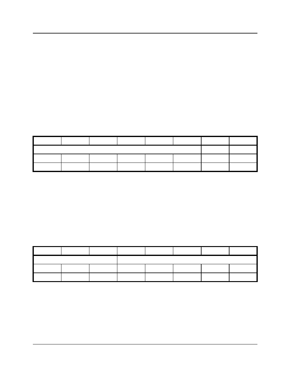
·Á
·Á
·Á
·Á
DS3/E3 FRAMER IC
XRT7250
REV. 1.1.1
103
insert flag sequence octets into the outbound LAPD chan-
nel, during the idle periods between transmissions.
Bit 2 - TxDL Busy
This Read-Only bit-field allows the user to poll or
monitor the status of the LAPD Transmitter to see if it
has completed its transmission of the LAPD Message
frame. The LAPD Transmitter will set this bit-field to
"1", while it is in the process of transmitting the LAPD
Message frame. However, the LAPD Transmitter will
clear this bit-field to "0" once it has completed its
transmission of the LAPD Message frame.
Bit 1 - TxLAPD Interrupt Enable
This Read/Write bit-field allows the user to enable or
disable the LAPD Message frame Transmission Com-
plete interrupt.
Writing a "0" to this bit-field disables this interrupt.
Writing a "1" to this bit-field enables this interrupt.
Bit 0 - TxLAPD Interrupt Status
This Reset-upon-Read bit-field allows the user to de-
termine if the LAPD Message Frame Transmission
Complete interrupt has occurred since the last read of
this register. If this bit-field contains a "1" then the
LAPD Message Frame Transmission Complete inter-
rupt has occurred since the last read of this register.
Conversely, if this bit-field contains a "0" then it has
not.
2.3.7.4
Transmit E3 Service Bits Register (ITU-
T G.751)
Bit 1 - A Bit
This Read/Write bit-field permits the user to define
the value of the A Bit within a given outbound E3
frame. If the user has configured the source of the A
Bit to be the TxE3 Service Bits Register (by setting
TxASource[1:0] = 00, within the TxE3 Configuration
Register, Address = 0x30), then the value written in
this bit-field will specify the value of the A Bit within
the outbound E3 Frame.
Bit 0 - N Bit
This Read/Write bit-field permits the user to define
the value of the N Bit within a given outbound E3
frame. If the user has configured the source of the N
Bit to be the TxE3 Service Bits Register (by setting
TxNSource[1:0] = 00, within the TxE3 Configuration
Register, Address = 0x30), then the value written in
this bit-field will specify the value of the N Bit within
the outbound E3 Frame.
2.3.7.5
Transmit E3 FAS Mask Register - 0
(ITU-T G.751)
Bits 4 - 0, TxFAS_Error_Mask_Upper[4:0]
This Read/Write bit-field permits the user to insert er-
rors into the upper five bits of the Framing Alignment
Signal, FAS of each outbound E3 frame. The user
may wish to do this for equipment testing purposes.
Prior to transmission, the Transmit E3 Framer block
reads in the upper five (5) bits of the FAS value, and
performs an XOR operation with it and the contents of
this register. The results of this operation are written
back into the upper five (5) bits of the FAS value, in
each outbound E3 frame. Consequently, to insure er-
rors are not injected into the FAS of the outbound E3
frames, the contents of this register must be set to all
"0's" (the default value).
2.3.7.6
Transmit E3 FAS Error Mask Register -
1 (ITU-T G.751)
TXE3 SERVICE BITS REGISTER (ADDRESS = 0X35)
B
IT
7
B
IT
6
B
IT
5
B
IT
4
B
IT
3
B
IT
2
B
IT
1
B
IT
0
Not Used
A Bit
N Bit
RO
RO
RO
RO
RO
RO
R/W
R/W
0
0
0
0
0
0
1
0
TXE3 FAS ERROR MASK REGISTER - 0 (ADDRESS = 0X48)
B
IT
7
B
IT
6
B
IT
5
B
IT
4
B
IT
3
B
IT
2
B
IT
1
B
IT
0
Not Used
TxFAS_Error_Mask_Upper[4:0]
RO
RO
RO
R/W
R/W
R/W
R/W
R/W
0
0
0
0
0
0
0
0

XRT7250
DS3/E3 FRAMER IC
·Á
·Á
·Á
·Á
REV. 1.1.1
104
Bits 4 - 0, TxFAS_Error_Mask_Lower[4:0]
This Read/Write bit-field permits the user to insert er-
rors into the lower five bits of the Framing Alignment
Signal, FAS of each outbound E3 frame. The user
may wish to do this for equipment testing purposes.
Prior to transmission, the Transmit E3 Framer block
reads in the lower five (5) bits of the FAS value, and
performs an XOR operation with it and the contents of
this register. The results of this operation are written
back into the lower five (5) bits of the FAS value, in
each outbound E3 frame. Consequently, to insure er-
rors are not injected into the FAS of the outbound E3
frames, the contents of this register must be set to all
"0's" (the default value).
2.3.7.7
Transmit E3 BIP-4 Error Mask Register
(ITU-T G.751)
Bits 3 - 0: TxBIP-4 Mask[3:0]
This Read/Write bit-field permits the user to insert er-
rors into the BIP-4 value within each outbound E3
frame. The user may wish to do this for equipment
testing purposes. Prior to transmission, the Transmit
E3 Framer reads in the BIP-4 value, and performs an
XOR operation with it and the contents of this regis-
ter. The results of this operation are written back into
the BIP-4 nibble position, in each outbound E3 frame.
Consequently, to insure errors are not injected into
the BIP-4 value of the outbound E3 frames, the con-
tents of this register must be set to all "0's" (the de-
fault value).
2.3.8
Performance Monitor Registers
2.3.8.1
PMON Line Code Violation Count Reg-
ister - MSB
This Reset-upon-Read register, along with the PMON
LCV Event Count Register - LSB (Address = 0x51)
contains a 16-bit representation of the number of Line
Code Violations that have been detected by the Re-
ceive E3 Framer, since the last read of these regis-
ters. This register contains the MSB (or Upper-Byte)
value of this 16 bit expression.
2.3.8.2
PMON Line Code Violation Count Reg-
ister - LSB
TXE3 FAS ERROR MASK REGISTER - 1 (ADDRESS = 0X49)
B
IT
7
B
IT
6
B
IT
5
B
IT
4
B
IT
3
B
IT
2
B
IT
1
B
IT
0
Not Used
TxFAS_Error_Mask_Lower[4:0]
RO
RO
RO
R/W
R/W
R/W
R/W
R/W
0
0
0
0
0
0
0
0
TXE3 BIP-4 ERROR MASK REGISTER (ADDRESS = 0X4A)
B
IT
7
B
IT
6
B
IT
5
B
IT
4
B
IT
3
B
IT
2
B
IT
1
B
IT
0
Not Used
TxBIP-4 Mask[3:0]
R/W
R/W
R/W
R/W
R/W
R/W
R/W
R/W
0
0
0
0
0
0
0
0
PMON LCV EVENT COUNT REGISTER - MSB (ADDRESS = 0X50)
B
IT
7
B
IT
6
B
IT
5
B
IT
4
B
IT
3
B
IT
2
B
IT
1
B
IT
0
LCV Count - High Byte
RUR
RUR
RUR
RUR
RUR
RUR
RUR
RUR
0
0
0
0
0
0
0
0
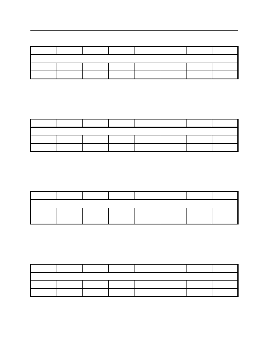
·Á
·Á
·Á
·Á
DS3/E3 FRAMER IC
XRT7250
REV. 1.1.1
105
This Reset-upon-Read register, along with the PMON
LCV Event Count Register - LSB (Address = 0x50)
contains a 16-bit representation of the number of Line
Code Violations that have been detected by the Re-
ceive E3 Framer, since the last read of these regis-
ters. This register contains the LSB (or Lower-Byte)
value of this 16 bit expression.
2.3.8.3
PMON Framing Bit/Byte Error Count
Register - MSB
This Reset-upon-Read register, along with the PMON
Framing Bit/Byte Error Count Register - LSB (Ad-
dress = 0x53) contains a 16-bit representation of the
number of Framing Bit or Byte Errors that have been
detected by the Receive DS3/E3 Framer, since the
last read of these registers. This register contains the
MSB (or Upper-Byte) value of this 16 bit expression.
2.3.8.4
PMON Framing Bit/Byte Error Count
Register - LSB
This Reset-upon-Read register, along with the PMON
Framing Bit/Byte Error Count Register - MSB (Ad-
dress = 0x52) contains a 16-bit representation of the
number of Framing Bit or Byte Errors that have been
detected by the Receive DS3/E3 Framer, since the
last read of these registers. This register contains the
LSB (or Lower-Byte) value of this 16 bit expression.
2.3.8.5
PMON Parity Error Count Register -
MSB
This Reset-upon-Read register, along with the PMON
Parity Error Count Register - LSB (Address = 0x55)
contains a 16-bit representation of the number of P-
bit Errors (for DS3 applications), BIP-4 Errors (for E3/
PMON LCV EVENT COUNT REGISTER - LSB (ADDRESS = 0X51)
B
IT
7
B
IT
6
B
IT
5
B
IT
4
B
IT
3
B
IT
2
B
IT
1
B
IT
0
LCV Count - Low Byte
RUR
RUR
RUR
RUR
RUR
RUR
RUR
RUR
0
0
0
0
0
0
0
0
PMON FRAMING BIT/BYTE ERROR COUNT REGISTER - MSB (ADDRESS = 0X52)
B
IT
7
B
IT
6
B
IT
5
B
IT
4
B
IT
3
B
IT
2
B
IT
1
B
IT
0
Framing Bit/Byte Error Count - High Byte
RUR
RUR
RUR
RUR
RUR
RUR
RUR
RUR
0
0
0
0
0
0
0
0
PMON FRAMING BIT/BYTE ERROR COUNT REGISTER - LSB (ADDRESS = 0X53)
B
IT
7
B
IT
6
B
IT
5
B
IT
4
B
IT
3
B
IT
2
B
IT
1
B
IT
0
Framing Bit/Byte Error Count - Low Byte
RUR
RUR
RUR
RUR
RUR
RUR
RUR
RUR
0
0
0
0
0
0
0
0
PMON PARITY ERROR COUNT REGISTER - MSB (ADDRESS = 0X54)
B
IT
7
B
IT
6
B
IT
5
B
IT
4
B
IT
3
B
IT
2
B
IT
1
B
IT
0
Parity Error Count - High Byte
RUR
RUR
RUR
RUR
RUR
RUR
RUR
RUR
0
0
0
0
0
0
0
0

XRT7250
DS3/E3 FRAMER IC
·Á
·Á
·Á
·Á
REV. 1.1.1
106
ITU-T G.751 applications) or BIP-8 Errors (for E3/
ITU-T G.832 applications) that have been detected by
the Receive DS3/E3 Framer, since the last read of
these registers. This register contains the MSB (or
Upper-Byte) value of this 16 bit expression.
2.3.8.6
PMON Parity Error Count Register -
LSB
This Reset-upon-Read register, along with the PMON
Parity Error Count Register - MSB (Address = 0x54)
contains a 16-bit representation of the number of P-
bit Errors (for DS3 applications), BIP-4 Errors (for E3/
ITU-T G.751 applications) or BIP-8 Errors (for E3/
ITU-T G.832 applications) that have been detected by
the Receive DS3/E3 Framer, since the last read of
these registers. This register contains the LSB (or
Lower-Byte) value of this 16 bit expression.
2.3.8.7
PMON FEBE Event Count Register -
MSB
This Reset-upon-Read register, along with the PMON
FEBE Event Count Register - LSB (Address = 0x57)
contains a 16-bit representation of the number of
FEBE Events that have been detected by the Receive
DS3/E3 Framer, since the last read of these registers.
This register contains the MSB (or Upper-Byte) value
of this 16 bit expression.
2.3.8.8
PMON FEBE Event Count Register -
LSB
This Reset-upon-Read register, along with the PMON
FEBE Event Count Register - MSB (Address = 0x56)
contains a 16-bit representation of the number of
FEBE Events that have been detected by the Receive
DS3/E3 Framer, since the last read of these registers.
This register contains the LSB (or Lower-Byte) value
of this 16 bit expression.
2.3.8.9
PMON CP-Bit Error Event Count Regis-
ter - MSB
PMON PARITY ERROR COUNT REGISTER - LSB (ADDRESS = 0X55)
B
IT
7
B
IT
6
B
IT
5
B
IT
4
B
IT
3
B
IT
2
B
IT
1
B
IT
0
Parity Error Count - Low Byte
RUR
RUR
RUR
RUR
RUR
RUR
RUR
RUR
0
0
0
0
0
0
0
0
PMON FEBE EVENT COUNT REGISTER - MSB (ADDRESS = 0X56)
B
IT
7
B
IT
6
B
IT
5
B
IT
4
B
IT
3
B
IT
2
B
IT
1
B
IT
0
FEBE Event Count - High Byte
RUR
RUR
RUR
RUR
RUR
RUR
RUR
RUR
0
0
0
0
0
0
0
0
PMON FEBE EVENT COUNT REGISTER - LSB (ADDRESS = 0X57)
B
IT
7
B
IT
6
B
IT
5
B
IT
4
B
IT
3
B
IT
2
B
IT
1
B
IT
0
FEBE Event Count - Low Byte
RUR
RUR
RUR
RUR
RUR
RUR
RUR
RUR
0
0
0
0
0
0
0
0
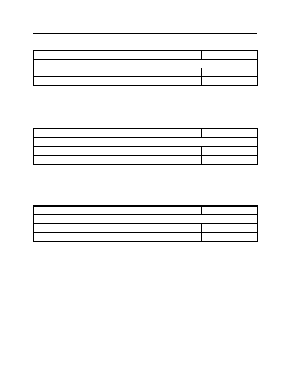
·Á
·Á
·Á
·Á
DS3/E3 FRAMER IC
XRT7250
REV. 1.1.1
107
This Reset-upon-Read register, along with the PMON
CP-Bit Error Count Register - LSB (Address = 0x59)
contains a 16-bit representation of the number of CP-
bit Errors that have been detected by the Receive
DS3 Framer block (within the chip), since the last
read of these registers. This register contains the
MSB (or Upper-Byte) value of this 16 bit expression.
2.3.8.10 PMON CP-Bit Error Event Count Regis-
ter - LSB
This Reset-upon-Read register, along with the PMON
CP-Bit Error Count Register - MSB (Address = 0x58)
contains a 16-bit representation of the number of CP-
bit Errors that have been detected by the Receive
DS3 Framer block (within the chip), since the last
read of these registers. This register contains the
LSB (or Lower-Byte) value of this 16 bit expression.
2.3.8.11 PMON Holding Register
Each of the PMON registers are 16 bit Reset-upon-
Read registers. More specifically, whenever the Mi-
croprocessor intends to read a PMON register, there
are two things to bear in mind.
1. This Microprocessor is going to require two read
accesses in order read out the full 16-bit expres-
sion of these PMON registers.
2. The entire 16-bit expression (of a given PMON
register) is going to be reset, immediately after
the Microprocessor has completed its first read
access to the PMON register.
Hence, the contents of the other byte (of the partially
read PMON register) will reside within the PMON
Holding register.
2.3.8.12 One-Second Error Status Register
PMON CP-BIT ERROR COUNT REGISTER - MSB (ADDRESS = 0X58)
B
IT
7
B
IT
6
B
IT
5
B
IT
4
B
IT
3
B
IT
2
B
IT
1
B
IT
0
CP-Bit Error Count - High Byte
RUR
RUR
RUR
RUR
RUR
RUR
RUR
RUR
0
0
0
0
0
0
0
0
PMON CP-BIT ERROR COUNT REGISTER - LSB (ADDRESS = 0X59)
B
IT
7
B
IT
6
B
IT
5
B
IT
4
B
IT
3
B
IT
2
B
IT
1
B
IT
0
CP-Bit Error Count - Low Byte
RUR
RUR
RUR
RUR
RUR
RUR
RUR
RUR
0
0
0
0
0
0
0
0
PMON HOLDING REGISTER (ADDRESS = 0X6C)
B
IT
7
B
IT
6
B
IT
5
B
IT
4
B
IT
3
B
IT
2
B
IT
1
B
IT
0
PMON Holding Value
RUR
RUR
RUR
RUR
RUR
RUR
RUR
RUR
0
0
0
0
0
0
0
0

XRT7250
DS3/E3 FRAMER IC
·Á
·Á
·Á
·Á
REV. 1.1.1
108
Bit 1 - Errored Second
This bit field indicates whether or not an error has oc-
curred within the last One-Second accumulation in-
terval. This bit-field will be set to "1" if at least one er-
ror has occurred during the last One-Second accu-
mulation interval. Conversely, this bit-field will be set
to "0" if no errors has occurred during the last one-
second accumulation interval.
Bit 0 - Severely Errored Second
This bit-field indicates whether or not the error rate in
the last one-second interval was greater than 1 in
103. A "0" indicates that the error rate did not exceed
1 in 103 in the last One-Second interval.
2.3.8.13 One-Second Line Code Violation Accu-
mulator Register - MSB
This Read-Only register, along with the LCV - One-
Second Accumulator Register - LSB (Address =
0x6F) contains a 16-bit representation of the number
of LCV (Line Code Violation) Events that have been
detected by the Receive DS3/E3 Framer block, within
the last one-second sampling period. This register
contains the MSB (or Upper-Byte) value of this 16 bit
expression.
2.3.8.14 One-Second Line Code Violation Accu-
mulator Register - LSB
This Read-Only register, along with the LCV - One-
Second Accumulator Register - MSB (Address =
0x6E) contains a 16-bit representation of the number
of LCV (Line Code Violation) Events that have been
detected by the Receive DS3/E3 Framer block, within
the last One-Second sampling period. This register
contains the LSB (or Lower-Byte) value of this 16 bit
expression.
2.3.8.15 One-Second Frame Parity Error Accu-
mulator Register - MSB
ONE-SECOND ERROR STATUS REGISTER (ADDRESS = 0X6D)
B
IT
7
B
IT
6
B
IT
5
B
IT
4
B
IT
3
B
IT
2
B
IT
1
B
IT
0
Errored
Second
Severely
Errored
Second
RO
RO
RO
RO
RO
RO
RO
RO
0
0
0
0
0
0
0
0
LCV - ONE-SECOND ACCUMULATOR REGISTER - MSB (ADDRESS = 0X6E)
B
IT
7
B
IT
6
B
IT
5
B
IT
4
B
IT
3
B
IT
2
B
IT
1
B
IT
0
LCV - One-Second Count - High Byte
RO
RO
RO
RO
RO
RO
RO
RO
0
0
0
0
0
0
0
0
LCV - ONE-SECOND ACCUMULATOR REGISTER - LSB (ADDRESS = 0X6F)
B
IT
7
B
IT
6
B
IT
5
B
IT
4
B
IT
3
B
IT
2
B
IT
1
B
IT
0
LCV - One-Second Count - Low Byte
RO
RO
RO
RO
RO
RO
RO
RO
0
0
0
0
0
0
0
0
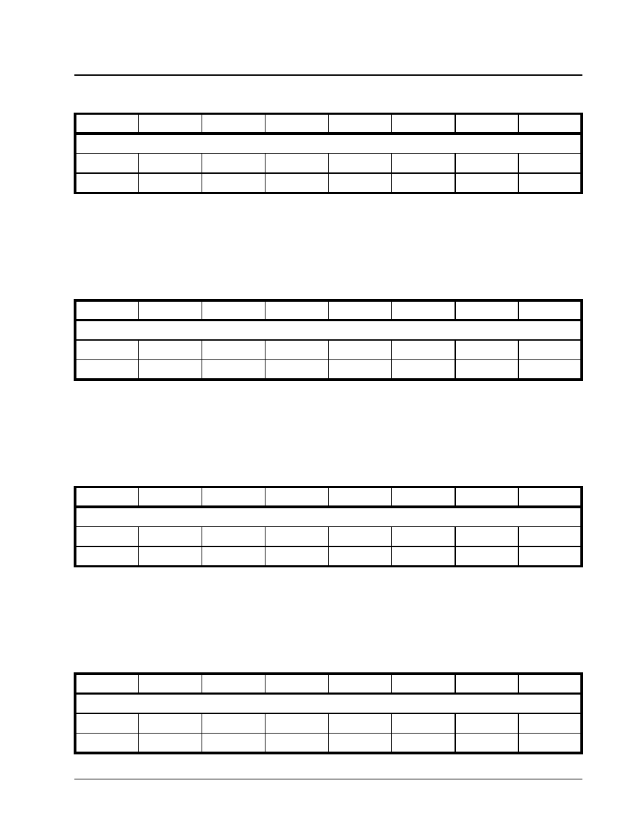
·Á
·Á
·Á
·Á
DS3/E3 FRAMER IC
XRT7250
REV. 1.1.1
109
This Read-Only register, along with the Frame Parity
Errors - One-Second Accumulator Register - LSB
(Address = 0x71) contains a 16-bit representation of
the number of Frame Parity Errors that have been de-
tected by the Receive DS3/E3 Framer block, within
the last One-Second sampling period. This register
contains the MSB (or Upper-Byte) value of this 16 bit
expression.
2.3.8.16 One-Second Frame Parity Error Accu-
mulator Register - LSB
This Read-Only register, along with the Frame Parity
Errors - One-Second Accumulator Register - MSB
(Address = 0x70) contains a 16-bit representation of
the number of Frame Parity Errors that have been de-
tected by the Receive DS3/E3 Framer block, within
the last one-second sampling period. This register
contains the LSB (or Lower-Byte) value of this 16 bit
expression.
2.3.8.17 One-Second Frame CP-Bit Error Accu-
mulator Register - MSB
This Read-Only register, along with the Frame CP-Bit
Error - One-Second Accumulator Register - LSB (Ad-
dress = 0x73) contains a 16-bit representation of the
number of CP Bit Errors tjhat have been detected by
the Receive DS3/E3 Framer block, within the last
one-second sampling period. This register contains
the MSB (or Upper Byte) value of this 16-bit expres-
sion.
2.3.8.18 One-Second Frame CP-Bit Error Accu-
mulator Register - LSB
FRAME PARITY ERRORS - ONE-SECOND ACCUMULATOR REGISTER - MSB (ADDRESS = 0X70)
B
IT
7
B
IT
6
B
IT
5
B
IT
4
B
IT
3
B
IT
2
B
IT
1
B
IT
0
Frame Parity Error Count - High Byte
RO
RO
RO
RO
RO
RO
RO
RO
0
0
0
0
0
0
0
0
FRAME PARITY ERRORS - ONE-SECOND ACCUMULATOR REGISTER - LSB (ADDRESS = 0X71)
B
IT
7
B
IT
6
B
IT
5
B
IT
4
B
IT
3
B
IT
2
B
IT
1
B
IT
0
Frame Parity Error Count - Low Byte
RO
RO
RO
RO
RO
RO
RO
RO
0
0
0
0
0
0
0
0
FRAME CP-BIT ERRORS - ONE-SECOND ACCUMULATOR REGISTER - MSB (ADDRESS = 0X72)
B
IT
7
B
IT
6
B
IT
5
B
IT
4
B
IT
3
B
IT
2
B
IT
1
B
IT
0
CP Bit Error Count - High Byte
RO
RO
RO
RO
RO
RO
RO
RO
0
0
0
0
0
0
0
0
FRAME PARITY ERRORS - ONE-SECOND ACCUMULATOR REGISTER - LSB (ADDRESS = 0X73)
B
IT
7
B
IT
6
B
IT
5
B
IT
4
B
IT
3
B
IT
2
B
IT
1
B
IT
0
CP Bit Error Count - Low Byte
RO
RO
RO
RO
RO
RO
RO
RO
0
0
0
0
0
0
0
0

XRT7250
DS3/E3 FRAMER IC
·Á
·Á
·Á
·Á
REV. 1.1.1
110
This Read-Only register, along with the Frame CP-Bit
Error - One-Second Accumulator Register - MSB (Ad-
dress = 0x72) contains a 16-bit representation of the
number of CP Bit Errors tjhat have been detected by
the Receive DS3/E3 Framer block, within the last
one-second sampling period. This register contains
the LSB (or Lower Byte) value of this 16-bit expres-
sion.
2.3.8.19 Line Interface Drive Register
Bit 5 - REQB - (Receive Equalization Bypass Con-
trol)
This Read/Write bit-field allows the user to control the
state of the REQB output pin of the UNI device. This
output pin is intended to be connected to EITHER OF
the REQB input pins of the XRT7300 DS3/E3 LIU IC.
If the user forces this signal to toggle "High", then the
Receive Equalizer (within the XRT7300 device) will
be disabled. Conversely, if the user forces this signal
to toggle "Low", then the Receive Equalizer (within
the XRT7300 device) will be enabled.
Writing a "1" to this bit-field causes the Framer device
to toggle the REQB output pin "High". Writing a "0" to
this bit-field causes the Framer device to toggle the
REQB output pin "Low".
For information on the criteria that should be used
when deciding whether to bypass the equalization cir-
cuitry or not, please consult the XRT7300 DS3/E3/
STS-1 LIU IC data sheet.
N
OTE
: If the customer is not using the XRT7300 DS3/E3/
STS-1 LIU IC, then this bit-field and the REQB output pin
can be used for other purposes.
Bit 4 - TAOS - (Transmit All Ones Signal)
This Read/Write bit-field allows the user to control the
state of the TAOS output pin of the UNI device. This
output pin is intended to be connected to the TAOS
input pin of the XRT7300 DS3/E3/STS-1 LIU IC. If
the user forces this signal to toggle "High", then the
XRT7300 LIU device will transmit an "All Ones" pat-
tern onto the line. Conversely, if the user commands
this output signal to toggle "Low" then the XRT7300
LIU IC will proceed to transmit data based upon the
pattern that it receives via the TxPOS and TxNEG
output pins (of the Framer IC).
Writing a "1" to this bit-field will cause the TAOS out-
put pin to toggle "High". Writing a "0" to this bit-field
will cause this output pin to toggle "Low".
N
OTE
: If the customer is not using the XRT7300 DS3/E3/
STS-1 LIU IC, then this bit-field, and the TAOS output pin
can be used for other purposes.
Bit 3 - Encodis - (B3ZS Encoder Disable)
This Read/Write bit-field allows the user to control the
state of the Encodis output pin of the UNI device.
This output pin is intended to be connected to the En-
codis input pin of the XRT7300 DS3/E3/STS-1 LIU
IC. If the user forces this signal to toggle "High", then
the internal B3ZS/HDB3 encoder (within the
XRT7300 device) will be disabled. Conversely, if the
user command this output signal to toggle "Low",
then the internal B3ZS/HDB3 encoder (within the
XRT7300 device) will be enabled.
Writing a "1" to this bit-field causes the Framer IC to
toggle the Encodis output pin "High". Writing a "0" to
this bit-field will cause the Framer IC to toggle this
output pin "Low".
N
OTES
:
1. The B3ZS/HDB3 encoder, within the XRT7300
device, is not to be confused with the B3ZS/HDB3
encoding capable that exists within the Transmit
Section of the Framer IC.
2. The user is advised to disabled the B3ZS/HDB3
encoder (within the XRT7300 IC) if the XRT7250 is
configured to operate in the B3ZS/HDB3 line code.
3. If the customer is not using the XRT7300 DS3/E3/
STS-1 LIU IC, then this bit-field and the Encodis
output pin can be used for other purposes.
4. It is permissible to tie the Encodis output pin of the
XRT7250 Framer IC to both the Encodis and Deco-
dis input pins of the XRT7300 device.
Bit 2 - TxLev - (Transmit Output Line Build-Out
Select Output)
This Read/Write bit-field allows the user to control the
state of the TxLev output pin of the Framer device.
This output pin is intended to be connected to the Tx-
Lev input pin of the XRT7300 DS3/E3/STS-1 LIU IC.
If the user commands this signal to toggle High, then
the XRT7300 DS3/E3/STS-1 LIU IC will disable the
LINE INTERFACE DRIVE REGISTER (ADDRESS = 0X80)
B
IT
7
B
IT
6
B
IT
5
B
IT
4
B
IT
3
B
IT
2
B
IT
1
B
IT
0
REQB
TAOS
ENCODIS
TxLEV
RLOOP
LLOOP
R/W
R/W
R/W
R/W
R/W
R/W
R/W
R/W
0
0
0
0
1
0
0
0

·Á
·Á
·Á
·Á
DS3/E3 FRAMER IC
XRT7250
REV. 1.1.1
111
Transmit Line Build-Out circuitry, and will transmit un-
shaped (square-wave) pulses onto the line. If the us-
er commands this signal to toggle "Low", then the
XRT7300 DS3/E3 LIU IC will enable the Transmit
Line Build-Out circuitry, and will transmit shaped puls-
es onto the line.
In order to insure that the transmit output pulses of
the XRT7300 device meet the DSX-3 Isolated Pulse
Template Requirements (per Bellcore GR-499-
CORE), the user is advised to set this bit-field to "0", if
the length of cable (between the XRT7300 transmit
output and the DSX-3 Cross Connect System) is
greater than 225 feet.
Conversely, the user is advised to set this bit-field to
"1", if the length of cable (between the XRT7300
transmit output and the DSX-3 Cross Connect sys-
tem) is less than 225 feet.
Writing a "1" to this bit-field commands the Framer to
toggle the TxLev output "High". Writing a "0" to this
bit-field commands the Framer to toggle this output
signal "Low".
N
OTES
:
1. The TxLEV function is only applicable to DS3 appli-
cations. E3 LIUs do not support this kind of Line
Build out feature.
2. If the customer is not using the XRT7300 or the
(XRT7296 DS3 Line Transmitter) IC, then this bit-
field and the TxLev output pin can be used for other
purposes.
Bit 1 - RLOOP - (Remote Loopback)
This Read/Write bit-field allows the user to control the
state of the RLOOP output pin of the Framer device.
This output pin is intended to be connected to the
RLOOP input pin of the XRT7300 DS3/E3 LIU IC.
In the XRT7300 DS3/E3 LIU IC, the state of the
RLOOP and the LLOOP pins are used to dictate
which loop-back mode the XRT7300 device will oper-
ate in. The following table presents the relationship
between the state of these two input pins (or bit-
fields) and the resulting loop-back modes.
Writing a "1" into this bit-field commands the Framer
IC to toggle the RLOOP output signal "High". Writing
a "0" into this bit-field commands the Framer IC to
toggle this output signal "Low".
For a detailed description of the XRT7300 DS3/E3
LIU's operation, during each of these above-men-
tioned loop-back modes, please consult the XRT7300
DS3/E3/STS-1 LIU IC Data Sheet.
N
OTE
: If the customer is not using the XRT7300 DS3/E3/
STS-1 LIU IC, then this bit-field and the RLOOP output pin
can be used for other purposes.
Bit 0 - LLOOP - (Local Loop-back)
This Read/Write bit-field allows the user to control the
state of the LLOOP output pin of the Framer device.
This output pin is intended to be connected to the
LLOOP input pin of the XRT7300 DS3/E3 LIU IC.
In the XRT7300 DS3/E3 LIU IC, the state of the
RLOOP and the LLOOP pins are used to dictate
which loop-back mode the XRT7300 device will oper-
ate in. The following table presents the relationship
between the state of these two input pins (or bit-
fields) and the resulting loop-back modes.
Writing a "1" into this bit-field commands the UNI to
toggle the LLOOP output signal "High". Writing a "0"
into this bit-field commands the Framer to toggle this
output signal "Low".
RLOOP
LLOOP
R
ESULTING
L
OOP
-
BACK
M
ODE
OF
THE
XRT7300 D
EVICE
0
0
Normal Operation (No Loop-back Mode)
0
1
Analog Local Loop-back Mode
1
0
Remote Loop-back Mode
1
1
Digital Local Loop-back Mode
RLOOP
LLOOP
R
ESULTING
L
OOP
-
BACK
M
ODE
OF
THE
XRT7300 D
EVICE
0
0
Normal Operation (No Loop-back Mode)
0
1
Analog Local Loop-back Mode
1
0
Remote Loop-back Mode
1
1
Digital Local Loop-back Mode

XRT7250
DS3/E3 FRAMER IC
·Á
·Á
·Á
·Á
REV. 1.1.1
112
For a detailed description of the XRT7300 DS3/E3
LIU's operation, during each of these above-men-
tioned loop-back modes, please consult the XRT7300
DS3/E3/STS-1 LIU IC Data Sheet.
N
OTE
: If the customer is not using the XRT7300 DS3/E3/
STS-1 LIU IC, then this bit-field and the LLOOP output pin
can be used for other purposes.
2.3.8.20 Line Interface Scan Register
Bit 2 - DMO - (Drive Monitor Output)
This Read-Only bit-field indicates the logic state of
the DMO input pin of the Framer device. This input
pin is intended to be connected to the DMO output
pin of the XRT7300 DS3/E3 LIU IC. If this bit-field
contains a logic "1", then the DMO input pin is "High".
The XRT7300 DS3/E3 LIU IC will set this pin "High" if
the drive monitor circuitry (within the XRT7300 de-
vice) has not detected any bipolar signals at the MTIP
and MRING inputs (of the XRT7300 device) within the
last 128 + 32 bit periods.
Conversely, if this bit-field contains a logic "0", then
the DMO input pin is "High". The XRT7300 DS3/E3
LIU IC will set this pin "Low" if bipolar signals are be-
ing detected at the MTIP and MRING input pins.
N
OTE
: If this customer is not using the XRT7300 DS3/E3
LIU IC, then this input pin can be used for a variety of other
purposes.
Bit 1 - RLOL - (Receive Loss of Lock)
This Read-Only bit-field indicates the logic state of
the RLOL input pin of the Framer device. This input
pin is intended to be connected to the RLOL output
pin of the XRT7300 DS3/E3 LIU IC. If this bit-field
contains a logic "1", then the RLOL input pin is
"High". The XRT7300 DS3/E3 LIU IC will set this pin
"High" if the clock recovery phase-locked-loop circuit-
ry (within the XRT7300 device) has lost lock with the
incoming DS3/E3 data-stream and is not properly re-
covering clock and data.
Conversely, if this bit-field contains a logic "0", then
the RLOL input pin is "Low". The XRT7300 DS3/E3
LIU IC will hold this pin "Low" as long as this clock re-
covery phase-locked-loop circuitry (within the
XRT7300 device) is properly locked onto the incom-
ing DS3 data-stream, and is properly recovering clock
and data from this data-stream.
For more information on the operation of the
XRT7300 DS3/E3/STS-1 LIU IC, please consult the
XRT7300 DS3/E3/STS-1 LIU IC data sheet.
N
OTE
: If the customer is not using the XRT7300 DS3/E3/
STS-1 IC, then this bit-field, and the RLOL input pin can be
used for other purposes.
Bit 0 - RLOS - (Receive Loss of Signal)
This Read-Only bit-field indicates the logic state of
the RLOS input pin of the Framer device. This input
pin is intended to be connected to the RLOS output
pin of the XRT7300 DS3/E3 LIU IC. If this bit-field
contains a logic "1", then the RLOS input pin is
"High". The XRT7300 device will toggle this signal
"High" if it (the XRT7300 LIU IC) is currently declaring
an LOS (Loss of Signal) condition.
Conversely, if this bit-field contains a logic "0", then
the RLOS input pin is "Low". The XRT7300 device
will hold this signal "Low" if it is NOT currently declar-
ing an LOS (Loss of Signal) condition.
For more information on the LOS Declaration and
Clearance criteria of the XRT7300 device, please
consult the XRT7300 DS3/E3/STS-1 LIU IC data
sheet.
N
OTE
: Asserting the RLOS input pin will cause the
XRT7250 Framer IC device to generate the Change in LOS
Condition interrupt and declare an LOS (Loss of Signal)
condition. Therefore, this input pin should not be used as a
general purpose input.
2.4
T
HE
L
OSS
OF
C
LOCK
E
NABLE
F
EATURE
The timing for the Microprocessor Interface section,
originates from a line rate (e.g., either a 34.368MHz
or 44.736 MHz) signal that is provided by either the
TxInClk or the RxLineClk signals. However, if the
Framer device experiences a Loss of Clock signal
event such that neither the TxInClk nor the RxLineClk
signal are present, then the Framer Microprocessor
Interface section cease to function.
The Framer device offers a Loss of Clock (LOC) pro-
tection feature that allows the Microprocessor Inter-
face section to at least complete or terminate an in-
process Read or Write cycle (with the local µP)
should this Loss of Clock event occur. The LOC cir-
cuitry consists of a ring oscillator that continuously
LINE INTERFACE SCAN REGISTER (ADDRESS = 0X81)
B
IT
7
B
IT
6
B
IT
5
B
IT
4
B
IT
3
B
IT
2
B
IT
1
B
IT
0
DMO
RLOL
RLOS
RO
RO
RO
RO
RO
RO
RO
RO
0
0
0
0
0
0
0
0

·Á
·Á
·Á
·Á
DS3/E3 FRAMER IC
XRT7250
REV. 1.1.1
113
checks for signal transitions at the TxInClk and RxLi-
neClk input pins. If a Loss of Clock Signal event oc-
cur such that no transitions are occurring on these
pins, then the LOC circuitry will automatically assert
the RDY_DTCK signal in order to complete (or termi-
nate) the current Read or Write cycle with the Framer
Microprocessor Interface section.
The user may enable or disable this LOC Protection
feature by writing to Bit 7 (LOC Enable) within the
Framer I/O Register, as depicted below.
Writing a "1" to this bit-field enables this LOC Protec-
tion feature. Writing a "0" to this bit-field disables this
feature.
N
OTE
: The Ring Oscillator can be a source of noise, within
the Framer chip. Hence, there may be situations where the
user will wish to disable the LOC Protection feature.
2.5
U
SING
THE
PMON H
OLDING
R
EGISTER
The Microprocessor Interface section consists of an
8-bit bi-directional data bus. As a consequence, the
local µP will be able to read from and write to the
Framer on-chip registers, 8 bit per (read or write) cy-
cle. Since most of the Framer on-chip registers con-
tain 8-bits, communicating with the local µP, over an
8-bit data bus, is not much of an inconvenience.
However, all of the PMON registers, within the Framer
IC, contain 16 bits. Consequently, any reads of the
PMON registers, will require two read cycles.
The XRT7250 Framer IC includes a feature that will
make reading a PMON register a slightly less compli-
cated task. The Framer chip address space contains
a register known as the PMON Holding register,
which is located at 0x6C. Whenever the local µP
reads in an 8-bit value of a given PMON registers
(e.g., either the upper-byte or the lower byte value of
the PMON register), the other 8-bit value of that
PMON register will automatically be accessible by
reading the PMON Holding register.
Hence, anytime the local µP is trying to read in the
contents of a PMON register, the first read access
must be made directly to one of the 8-bit values of the
PMON registers (e.g., for example: the PMON LCV
Event Count Register - MSB, Address = 0x50). How-
ever, the second read can always be made to a con-
stant location in system memory, the PMON Holding
Register.
2.6
T
HE
I
NTERRUPT
S
TRUCTURE
WITHIN
THE
F
RAMER
M
ICROPROCESSOR
I
NTERFACE
S
ECTION
The XRT7250 Framer device is equipped with a so-
phisticated Interrupt Servicing Structure. This Inter-
rupt Structure includes an Interrupt Request output,
INT, numerous Interrupt Enable Registers and numer-
ous Interrupt Status Registers. The Interrupt Servic-
ing Structure, within the Framer contains two levels of
hierarchy. The top level is at the functional block level
(e.g., the Receive Section, the Transmit Section, etc.).
The lower hierarchical level is at the individual inter-
rupt or source level. Each hierarchical level consists
of a complete set of Interrupt Status Registers/bits
and Interrupt Enable Registers/bits, as will be dis-
cussed below.
Both of the functional sections, within the Framer, are
capable of generating Interrupt Requests to the local
µP/µC. The Framer device Interrupt Structure has
been carefully designed to allow the user to quickly
determine the exact source of the interrupt (with mini-
mal latency) which will aid the local µP/µC in deter-
mining which interrupt service routine to call up in or-
der to respond to or eliminate the condition(s) caus-
ing the interrupt.
Table 5 lists all of the possible conditions that can
generate interrupts, with each functional section of
the Framer IC.
ADDRESS = 0X01, FRAMER I/O CONTROL REGISTER
B
IT
7
B
IT
6
B
IT
5
B
IT
4
B
IT
3
B
IT
2
B
IT
1
B
IT
0
LOC Enable
Test PMON
Interrupt
Enable
Reset
AMI/B3ZS*
Unipolar/
Bipolar*
TxLine
Clk Inv
RxLine
Clk Inv
Reframe
R/W
R/W
R/W
R/W
R/W
R/W
R/W
R/W
1
0
1
0
0
0
0
0

XRT7250
DS3/E3 FRAMER IC
·Á
·Á
·Á
·Á
REV. 1.1.1
114
The XRT7250 Framer Interrupt Block comes
equipped with the following registers to support the
servicing of these potential interrupt request sources.
Table 6, 7 , and 8 lists these registers, and their ad-
dresses, within the Framer IC for DS3, E3 (ITU-T
G.832) and E3 (ITU-T G.751) framing formats.
T
ABLE
5: L
IST
OF
ALL
OF
THE
P
OSSIBLE
C
ONDITIONS
THAT
CAN
G
ENERATE
I
NTERRUPTS
WITHIN
THE
XRT7250
F
RAMER
D
EVICE
F
UNCTION
S
ECTION
I
NTERRUPTING
C
ONDITION
Transmit Section
FEAC Message Transfer Complete (DS3, C-Bit Parity Only)
LAPD Message frame Transfer Complete (DS3, C-Bit Parity, All E3)
Receive Section
Change of Status on Receive LOS, OOF, AIS Idle Detection
Validation and removal of received FEAC Code (DS3, C-Bit Parity Only)
New PMDL Message in Receive LAPD Message Buffer.
Detection of Parity Errors (e.g., P-Bit, CP-Bit, BIP-4 and BIP-8 Errors)
Detection of Framing Bit/Byte Errors.
Framer Chip Level
One-Second Interrupt
T
ABLE
6: A L
ISTING
OF
THE
XRT7250 F
RAMER
D
EVICE
I
NTERRUPT
B
LOCK
R
EGISTERS
(
FOR
DS3 A
PPLICATIONS
)
A
DDRESS
L
OCATION
R
EGISTER
N
AME
0 x 04
Block Interrupt Enable Register
0 x 05
Block Interrupt Status Register
0 x 12
RxDS3 Interrupt Enable Register
0 x 13
RxDS3 Interrupt Status Register
0 x 17
RxDS3 FEAC Interrupt Enable/Status Register
0 x 18
RxDS3 LAPD Control Register
0 x 31
TxDS3 FEAC Configuration and Status Register
0 x 34
TxDS3 LAPD Status/Interrupt Register
T
ABLE
7: A L
ISTING
OF
THE
XRT7250 F
RAMER
D
EVICE
I
NTERRUPT
B
LOCK
R
EGISTERS
(
FOR
E3, ITU-T G.832
A
PPLICATIONS
)
A
DDRESS
L
OCATION
R
EGISTER
N
AME
0 x 04
Block Interrupt Enable Register
0 x 05
Block Interrupt Status Register
0 x 12
RxE3 Interrupt Enable Register -1
0 x 13
RxE3 Interrupt Enable Register -2
0 x 14
RxE3 Interrupt Status Register - 1
0 x 15
RxE3 Interrupt Status Register - 2
0 x 18
RxE3 LAPD Control Register
0 x 34
TxE3 LAPD Status/Interrupt Status

·Á
·Á
·Á
·Á
DS3/E3 FRAMER IC
XRT7250
REV. 1.1.1
115
General Flow of Framer Chip Interrupt Servicing
When any of the conditions, presented in Table 5 oc-
curs, (if their Interrupts is enabled), then the Framer
will generate an interrupt request to the local µP/µC
by asserting the active-low interrupt request output
pin, INT. Shortly after the local µP/µC has detected
the activated INT signal, it will enter into the appropri-
ate user-supplied interrupt service routine. The first
task for the local µP/µC, while running this interrupt
service routine, may be to isolate the source of the in-
terrupt request down to the device level (e.g., the
XRT7250 Framer Device), if multiple peripheral devic-
es exist in the user's system. However, once the in-
terrupting peripheral device has been identified, the
next task for the local µP/µC is to determine exactly
what feature or functional section within the device re-
quested the interrupt.
Determine the Functional Block(s) Requesting the
Interrupt
If the interrupt device turns out to be the XRT7250
DS3/E3 Framer IC, then the local µC/µP must deter-
mine which functional block requested the interrupt.
Hence, upon reaching this state, one of the very first
things that the local µC/µP must do within the user
supplied Framer Interrupt Service routine, is to per-
form a read of the Block Interrupt Status Register
(Address = 0x05) within the XRT7250 Framer device.
The bit format of the Block Interrupt Status register is
presented below.
The Block Interrupt Status Register presents the in-
terrupt request status of each functional block, within
the chip. The purpose of the Block Interrupt Status
Register is to help the local µP/µC identify which func-
tional block(s) has requested the interrupt. Whichev-
er bit(s) are asserted in this register, identifies which
block(s) have experienced an interrupt-generating
condition as presented in Table 5. Once the local µP/
µC has read this register, it can determine which
branch within the interrupt service routine that it must
follow, in order to properly service this interrupt.
The Framer further supports the Functional Block hi-
erarchy by providing the Block Interrupt Enable Reg-
ister (Address = 0x04). The bit format of this register
is identical to that for the Block Interrupt Status regis-
ter, and is presented below for the sake of complete-
ness.
T
ABLE
8: A L
ISTING
OF
THE
XRT7250 F
RAMER
D
EVICE
I
NTERRUPT
B
LOCK
R
EGISTER
(
FOR
E3, ITU-T G.751
A
PPLICATIONS
)
A
DDRESS
L
OCATION
R
EGISTER
N
AME
0 x 04
Block Interrupt Enable Register
0 x 05
Block Interrupt Status Register
0 x 12
RxE3 Interrupt Enable Register -1
0 x 13
RxE3 Interrupt Enable Register -2
0 x 14
RxE3 Interrupt Status Register - 1
0 x 15
RxE3 Interrupt Status Register - 2
0 x 18
RxE3 LAPD Control Register
0 x 34
TxE3 LAPD Status/Interrupt Status
BLOCK INTERRUPT STATUS REGISTER (ADDRESS = 0X05)
B
IT
7
B
IT
6
B
IT
5
B
IT
4
B
IT
3
B
IT
2
B
IT
1
B
IT
0
RxDS3/E3
Interrupt
Status
Not Used
TxDS3/E3
Interrupt
Status
One-Second
Interrupt
Status
RO
RO
RO
RO
RO
RO
RO
RO
0
0
0
0
0
0
0
0

XRT7250
DS3/E3 FRAMER IC
·Á
·Á
·Á
·Á
REV. 1.1.1
116
The Block Interrupt Enable register allows the user to
individually enable or disable the interrupt requesting
capability of the functional blocks, within the Framer
IC. If a particular bit-field, within this register contains
the value "0", then the corresponding functional block
has been disabled from generating any interrupt re-
quests. Conversely, if that bit-field contains the value
"1", then the corresponding functional block has been
enabled for interrupt generation (e.g., those potential
interrupts, within the enabled functional block that are
enabled at the source level, are now enabled). The
user should be aware of the fact that each functional
block, within the Framer IC contains anywhere from 1
to 12 potential interrupt sources. Each of these lower
level interrupt sources contain their own set of inter-
rupt enable bits and interrupt status bits, existing in
various on-chip registers.
Interrupt Service Routing Branching: after reading
the Block Interrupt Status Register.
The contents of the Block Interrupt Status Register
identify which of 3 functional blocks (within the Fram-
er IC) has requested interrupt service. The local µP
should use this information in order to determine
where, within the Interrupt Service Routing, program
control should branch to. Table 9 can be viewed as
an interrupt service routine guide. It lists each of the
Functional Blocks, that contain a bit-field in the Block
Interrupt Status Register. Additionally, this table also
presents a list and addresses of corresponding on-
chip Registers that the Interrupt Service Routine
should branch to and read, based upon the Interrupt-
ing Functional Block.
Table 9, Table 10, and Table 11 presents the Interrupt
Service Routine guide for DS3, E3/ITU-T G.832 and
E3/ITU-T G.751 applications, respectively.
BLOCK INTERRUPT ENABLE REGISTER (ADDRESS = 0X04)
B
IT
7
B
IT
6
B
IT
5
B
IT
4
B
IT
3
B
IT
2
B
IT
1
B
IT
0
RxDS3/E3
Interrupt
Status
Not Used
TxDS3/E3
Interrupt
Status
One-Second
Interrupt
Status
R/W
RO
RO
RO
RO
RO
R/W
R/W
0
0
0
0
0
0
0
0
T
ABLE
9: I
NTERRUPT
S
ERVICE
R
OUTINE
G
UIDE
(
FOR
DS3 A
PPLICATIONS
)
I
NTERRUPTING
F
UNCTIONAL
B
LOCK
T
HE
N
EXT
R
EGISTERS
TO
BE
R
EAD
D
URING
THE
I
NTERRUPT
S
ERVICE
R
OUTINE
R
EGISTER
A
DDRESS
Receive Section
RxDS3 Interrupt Status Register
0 x 013
RxDS3 FEAC Interrupt Enable/Status Register
0 x 17
RxDS3 LAPD Control Register
0 x 18
Transmit Section
TxDS3 FEAC Configuration and Status Register
0 x 31
TxDS3 LAPD Status/Interrupt Register
0 x 34

·Á
·Á
·Á
·Á
DS3/E3 FRAMER IC
XRT7250
REV. 1.1.1
117
Once the Microprocessor/Microcontroller has read
the register that corresponds to the interrupting
source within the Framer, the following things will
happen.
1. The Asserted Interrupt Status bit-fields within this
register will be reset upon read.
2. The Asserted bit-field, within the Block Interrupt
Status register will be reset.
3. The Framer device will negate the INT (Interrupt
Request) output pin, by drving this output pin
"High".
2.6.1
Automatic Reset of Interrupt Enable Bits
Occassionally, the user's system (which includes the
Framer device) may experience a fault condition,
such that a Framer Interrupt Condition will continu-
ously exist. If this particular interrupt condition has
been enabled (within the Framer IC) then the Framer
device will generate an interrupt request to the MIcro-
processor/Microcontroller. Afterwards, the Micropro-
cessor/Microcontroller will attempt to service this in-
terrupt by reading the Block Interrupt Status register
and the subsequent source level interrupt status reg-
isters. Additionally, the Microprocessor/Microcontrol-
ler will attempl to perform some system-related tasks
in order to try to resolve those conditions causing the
interrupt. After the Microprocessor/Microcontroller
has attempted all of these things, the Framer IC will
negate the INT output pin. However, because the
system fault still remains, the conditions causing the
Framer to issue this interrupt request, also still exists.
Consequently, the Framer device will generate anoth-
er interrupt request, which forces the Microprocessor/
Microcontroller to once again attempt to service this
interrupt. This phenomenon quickly results in the lo-
cal Microprocessor/Microcontroller being tied up in a
continuous cycle of executing this one interrupt ser-
vice routine. Consequently, the local Microprocessor/
Microcontroller (along with portions of the overall sys-
tem) now becomes non-functional.
In order to prevent this phenomenon from ever occur-
ing, the Framer IC allows the user to automatically re-
set the interrupt enable bits, following their activation.
The user can implement this feature by writing the ap-
propriate value into Bit 3 (Interrupt Enable Reset)
within the Framer Operating Mode register, as illus-
trated below.
T
ABLE
10: I
NTERRUPT
S
ERVICE
R
OUTINE
G
UIDE
(
FOR
E3, ITU-T G.832 A
PPLICATIONS
)
I
NTERRUPTING
F
UNCTIONAL
B
LOCK
T
HE
N
EXT
R
EGISTERS
TO
BE
R
EAD
D
URING
THE
I
NTERRUPT
S
ERVICE
R
OUTINE
R
EGISTER
A
DDRESS
Receive Section
RxE3 Interrupt Status Register - 1
0 x 014
RxE3 Interrupt Status Register - 2
0 x 15
RxE3 LAPD Control Register
0 x 18
Transmit Section
TxE3 LAPD Status and Interrupt Register
0 x 34
T
ABLE
11: I
NTERRUPT
S
ERVICE
R
OUTINE
G
UIDE
(
FOR
E3, ITU-T G.751 A
PPLICATIONS
)
I
NTERRUPTING
F
UNCTIONAL
B
LOCK
T
HE
N
EXT
R
EGISTERS
TO
BE
R
EAD
D
URING
THE
I
NTERRUPT
S
ERVICE
R
OUTINE
R
EGISTER
A
DDRESS
Receive Section
RxE3 Interrupt Status Register - 1
0 x 014
RxE3 Interrupt Status Register - 2
0 x 15
RxE3 LAPD Control Register
0 x 18
Transmit Section
TxE3 LAPD Status and Interrupt Register
0 x 34

XRT7250
DS3/E3 FRAMER IC
·Á
·Á
·Á
·Á
REV. 1.1.1
118
Writing a "1" to this bit-field configures the Framer to
automatically disable a given interrupt, following its
activation. Writing a "0" to this bit-field configures the
Framer to leave the Interrupt Enable bit as is, follow-
ing interrupt activation.
If a user opts to implement the Automatic Reset of In-
terrupt Enable Bits feature, then he/she might wish to
configure the Microprocessor/Microcontroller to go
back and re-enable these interrupts at a later time.
2.6.2
One-Second Interrupts
The Block Interrupt Status register, and Block Inter-
rupt Enable register each contain a bit-field for the
One-Second Interrupt. If this interrupt is enabled
(within the Block Interrupt Enable register), then the
Framer device will automatically generate an interrupt
request to the Microprocessor/Microcontroller repeat-
edly at one-second intervals. At a minimum, the us-
er's interrupt service routine must service this inter-
rupt by reading the Block Interrupt Status register
(Address = 0x05). Once the Microprocessor/Micro-
controller has read this register, then the following
things will happen.
1. The One-Second Interrupt bit-field, within the
Block Interrupt Status register, will be reset to "0".
2. The Framer will negate the INT (Interrupt
Request) output pin.
The purpose of providing this One-Second interrupt is
to allow the Microprocessor/Microcontroller the op-
portunity to perform certain tasks at One-Second in-
tervals. The user can accomplish this by including
the necessary code (for these various tasks) as a part
of the interrupt service routine, for the One-Second
type interrupt. Some of these tasks could include:
∑ Reading in the contents of the One-Second Perfor-
mance Monitor registers.
∑ Reading various other Performance Monitor regis-
ters.
∑ Writing a new PMDL Message into the Transmit
LAPD Message buffer. After the LAPD Transmitter
has been enabled and commanded to initiate trans-
mission of the LAPD Message frame (containing
the PMDL Message, residing within the Transmit
LAPD Message buffer), the LAPD Transmitter will
continue to re-transmit this same LAPD Message
frame, repeatedly at One-Second intervals, until it
has been disabled. If a new PMDL message is
written into the Transmit LAPD Message buffer
immediately following the occurrence of a One-Sec-
ond Interrupt, then this will ensure that this Write
activity will not interfere with this periodic transmis-
sion of the LAPD Message frames.
Notes regarding the Block Interrupt Enable and Block
Interrupt Status Registers:
1. The Block Interrupt Enable Register allows the
user to globally disable all potential interrupts
within either the Transmit or Receive sections, by
writing a "0" into the appropriate bit-field of this
register. However, the Block Interrupt Enable
register does not allow the user to globally enable
all potential interrupts within a given functional
block. In other words, enabling a given functional
block does not automatically enable all of its
potential interrupt sources. Those potential inter-
rupt sources that have been disabled at the
source level will remain disabled, independent of
the status of their associated functional blocks.
2. The Block Interrupt Enable register is set to
"0x00" upon power or reset. Therefore, the user
will have to write some "1's" into this register, in
order to enable some of the interrupts.
The remaining registers, listed in Table 9, Table 10
and Table 11 will be presented in the discussion of
the functional blocks, within the XRT7250 Framer IC.
These discussions will present more details about the
interrupt causes and how to properly service. them.
2.7
I
NTERFACING
THE
FRAMER
TO
AN
INTEL
-
TYPE
MICROPROCESSOR
The Framer can be interfaced to either Intel-type or
Motorola-type Microprocessor/Microcontrollers. The
following sections will provide one example for each
type of processor. This section discusses how to in-
terface the XRT7250 DS3/E3 Framer IC to the 8051
Microcontroller.
FRAMER OPERATING MODE REGISTER (ADDRESS = 0X00)
B
IT
7
B
IT
6
B
IT
5
B
IT
4
B
IT
3
B
IT
2
B
IT
1
B
IT
0
Local
Loop-Back
DS3/E3
Internal
LOS Enable
RESET
Interrupt
Enable Reset
Frame Format
TimRefSel[1:0]
R/W
R/W
R/W
R/W
R/W
R/W
R/W
R/W
0
0
0
0
0
0
0
0

·Á
·Á
·Á
·Á
DS3/E3 FRAMER IC
XRT7250
REV. 1.1.1
119
The 8051 Microcontroller
The 8051 family of microcontrollers is manufactured
by Intel and comes with a variety of amenities. Some
of these amenities include:
∑ On-chip Serial Port
∑ Four (4) 8-bit I/O ports (P0 - P3)
∑ 4k bytes of ROM
∑ 128 bytes of RAM
The 8051 Microcontroller consists of 4 - 8-bit I/O
Ports. Some of these ports have alternate functions
as will be discussed below.
PORT 0 (P0.0 - P0.7)
This port is a dual-purpose port on pins 32-39 of the
8051 IC. In minimal component designs, it is used as
a general purpose I/O port. For larger designs with
external memory, it becomes a multiplexed address
and data bus (AD0 - AD7).
PORT 1 (P1.0 - P1.7)
Port 1 is a dedicated port on pins 1 - 8. The pins,
designated at P1.0, P1.1, ... P1.7 are available for in-
terfacing as required. No alternative functions are as-
signed for Port 1 pins, thus they are used solely for in-
terfacing external devices. Exceptions are the 8032
and 8052 ICs, which use P1.0 and P1.1 as either as I/
O lines or as extenal inputs to the third timer.
PORT 2 (P2.0 - P2.7)
Port 2 (pins 21 - 28) is a dual-purpose port that can
function as a general purpose I/O, or as the high-byte
of the address bus for designs with external code
memory of more than 256 bytes of external data
memory (A8 - A15).
PORT 3
Port 3 is a dual purpose port on pins 10 - 17. In addi-
tion to functioning as general purpose I/O, these pins
have multiple functions. Each of these pins have an
alternate purpose, as listed in Table 12 below.
The 8051 also has numerous additional pins which
are relevant to interfacing to the XRT7250 DS3/E3
UNI or other peripherals. These pins are:
ALE - Address Latch Enable
If Port 0 is used in its alternative mode -as the data
bus and the lower byte of the address bus -- ALE is
the signal that latches the address into an external
register during the first half of a memory cycle. Once
this is done, Port 0 lines are then available for data in-
put or output during the second half of the memory
cycle, when the data transfer takes place.
INT0* (P3.2) and INT1* (P3.3)
INT0* and INT1* are external interrupt request inputs
to the 8051 Microcontroller. Each of these interrupt
pins support direct interrupt processing. In this case,
the term direct means that if one of these inputs are
asserted, then program control will automatically
branch to a specific (fixed) location in code memory.
This location is determined by the circuit design of the
8051 Microcontroller IC and cannot be changed.
Table 13 presents the location (in code memory)
where the program control will branch to, if either of
these inputs are asserted.
T
ABLE
12: A
LTERNATE
F
UNCTIONS
OF
P
ORT
3 P
INS
B
IT
N
AME
A
LTERNATE
F
UNCTION
P3.0
RXD
Receive Data for Serial Port
P3.1
TXD
Transmit Data for Serial Port
P3.2
INT0*
External Interrupt 0
P3.3
INT1*
External Interrupt 1
P3.4
T0
Timer/Counter 0 External Input
P3.5
T1
Timer/Counter 1 External Input
P3.6
WR*
External Data/Memory Write Strobe
P3.7
RD*
External Data/Memory Read Strobe
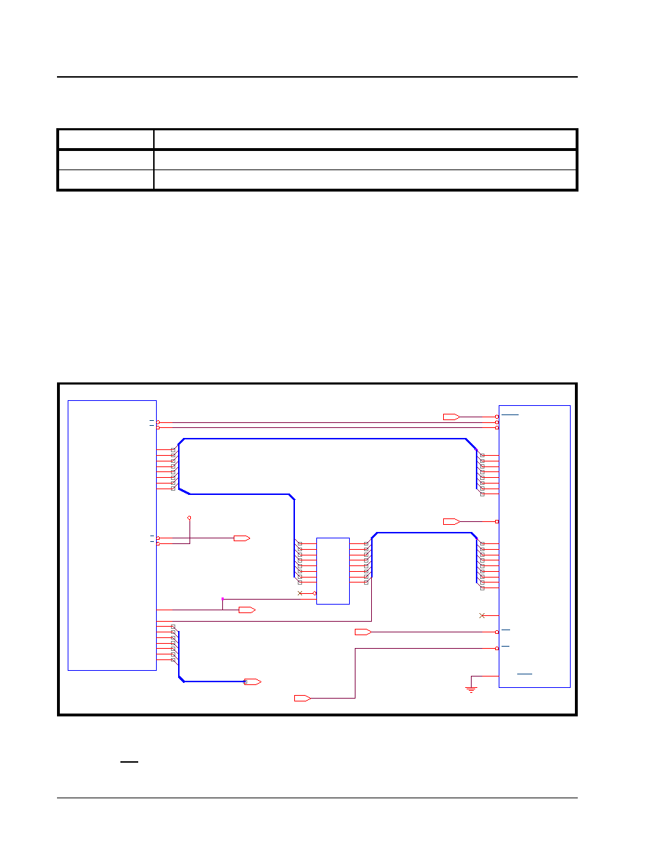
XRT7250
DS3/E3 FRAMER IC
·Á
·Á
·Á
·Á
REV. 1.1.1
120
Therefore, if the user is using either one of these in-
puts as an interrupt request input, then the user must
ensure that the appropriate interrupt service routine
or unconditional branch instruction (to the interrupt
service routine) is located at one of these address lo-
cations.
If the 8051 Microcontroller IC is required to interface
to external components in the data memory space of
sizes greater than 256 bytes, then both Ports 0 and 2
must be used as the address and data lines. Port 0
will function as a multiplexed address/data bus. Dur-
ing the first half of a memory cycle, Port 0 will operate
as the lower address byte. During the second half of
the memory cycle, Port 0 will operate as the bi-direc-
tional data bus. Port 2 will be used as the upper ad-
dress byte. ALE and the use of a 74HC373 transpar-
ent latch device can be used to de-multiplex the Ad-
dress and Data bus signals.
Figure 37 presents a schematic illustrating how the
XRT7250 DS3/E3 Framer can be interfaced to the
8051 Microcontroller IC.
The circuitry in Figure 37 will function as follows, dur-
ing a Framer-request interrupt. The Framer device
would request an interrupt from the CPU by asserting
its active low INT output pin. This will cause the
INT0* input pin of the CPU to go "Low". When this
happens the 8051 CPU will finish executing its cur-
rent instruction, and will then branch program control
to the Framer Device interrupt service routine. In the
case of Figure 37, the interrupt service routine will be
located in 0x0003 in code memory. The 8051 CPU
T
ABLE
13: I
NTERRUPT
S
ERVICE
R
OUTINE
L
OCATION
(
IN
C
ODE
M
EMORY
)
FOR
THE
INT0*
AND
INT1* I
NTERRUPT
I
NPUT
PINS
I
NTERRUPT
PIN
B
RANCH
TO
LOCATION
(
IN
S
YSTEM
M
EMORY
)
INT0*
0x0003
INT1*
0x0013
F
IGURE
37. S
CHEMATIC
DEPICTING
HOW
TO
INTERFACE
THE
XRT7250 DS3/E3 F
RAMER
IC
TO
THE
8051 M
ICRO
-
CONTROLLER
+ 5 V
U 2
8 0 5 1
W R
1 6
R D
1 7
A D 0
3 9
A D 1
3 8
A D 2
3 7
A D 3
3 6
A D 4
3 5
A D 5
3 4
A D 6
3 3
A D 7
3 2
A L E
3 0
A 8
2 1
A 9
2 2
A 1 0
2 3
A 1 1
2 4
A 1 2
2 5
A 1 3
2 6
A 1 4
2 7
A 1 5
2 8
I N T 0
1 2
I N T 1
1 3
U 1
X R T 7 2 5 0
R E S E T
2 8
R D B _ D S
2 9
A L E _ A S
3 1
INT
1 3
C S
8
W R B _ R W
7
D 0
3 2
D 1
3 3
D 2
3 4
D 3
3 5
D 4
3 6
D 5
3 7
D 6
3 8
D 7
3 9
A 0
1 4
A 1
1 5
A 2
1 6
A 3
1 7
A 4
1 8
A 5
1 9
A 6
2 0
A 7
2 1
A 8
2 2
M O T O / I N T E L
2 7
R d y _ D t c k
6
U ?
7 4 H C 3 7 3
D 0
3
D 1
4
D 2
7
D 3
8
D 4
1 3
D 5
1 4
D 6
1 7
D 7
1 8
O C
1
G
1 1
Q 0
2
Q 1
5
Q 2
6
Q 3
9
Q 4
1 2
Q 5
1 5
Q 6
1 6
Q 7
1 9
to Address Decoder
f r o m A d d r e s s D e c o d e r
A L E
A L E
I N T E R R U P T
I N T E R R U P T
R E S E T C o m m a n d C i r c u i t r y
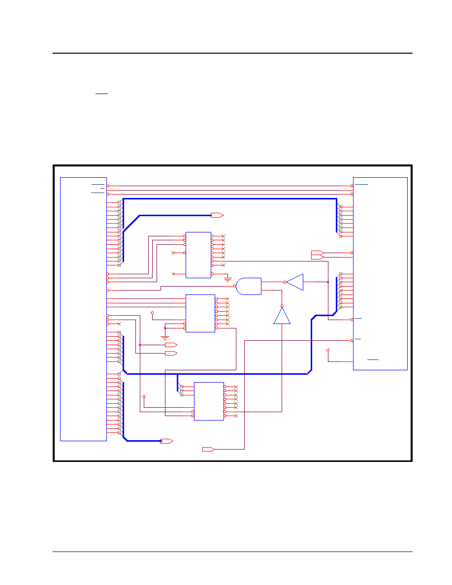
·Á
·Á
·Á
·Á
DS3/E3 FRAMER IC
XRT7250
REV. 1.1.1
121
does not issue an Interrupt Acknowledge signal back
to the Framer IC. It will just begin processing through
the Framer's interrupt service routine. One the CPU
has eliminated the cause(s) of the interrupt request,
the Framer's INT output pin will be negated (e.g., go
"High") and the CPU will return from the Interrupt Ser-
vice Routine and resume normal operation.
2.8
I
NTERFACING
THE
F
RAMER
IC
TO
A
M
OTOROLA
-
TYPE
M
ICROPROCESSOR
This section discusses how to interface the XRT7250
DS3/E3 Framer IC to the MC68000 Microprocessor.
Figure 38 presents a schematic on how to interface
the XRT7250 DS3/E3 Framer IC to the MC68000 Mi-
croprocessor, over an 8-bit wide bi-directional data
bus.
In general, the approach to interfacing these two de-
vices is pretty straightforward. However, the user
must be aware of the fact that the XRT7250 DS3/E3
Framer IC does not provide an interrupt vector to the
MC68000 during an Interrupt Acknowledge cycle.
Therefore, the user must configure his/her design to
support auto-vectored interrupts. Auto-vectored in-
terrupt processing is a feature offered by the
MC68000 Family of Microprocessors, where, if the
microprocessor knows (prior to any IACK cycle) the
Interrupt Level of this current interrupt, and that the
interrupting peripheral does not support vectored in-
terrupts, then the Microprocessor will generate its
own Interrupt Vector. The schematic shown in
Figure 38, has been configured to support auto-vec-
tored interrupts.
F
IGURE
38. S
CHEMATIC
D
EPICTING
HOW
TO
INTERFACE
THE
XRT7250 DS3/E3 F
RAMER
IC
TO
THE
MC68000
M
ICROPROCESSOR
+ 5 V
+ 5 V
+ 5 V
U 2
M C 6 8 0 0 0
R E S E T
18
R / W
9
D T A C K
10
D 0
5
D 1
4
D 2
3
D 3
2
D 4
1
D 5
64
D 6
63
D 7
62
D 8
61
D 9
60
D 1 0
59
D 1 1
58
D 1 2
57
D 1 3
56
D 1 4
55
D 1 5
54
A 1
29
A 2
30
A 3
31
A 4
32
A 5
33
A 6
34
A 7
35
A 8
36
A 9
37
F C 0
28
F C 1
27
F C 2
26
V P A
21
IPL0
25
IPL1
24
IPL2
23
A S
6
U D S
7
L D S
8
A 1 0
38
A 1 1
39
A 1 2
40
A 1 3
41
A 1 4
42
A 1 5
43
A 1 6
44
A 1 7
45
A 1 8
46
A 1 9
47
A 2 0
48
A 2 1
49
A 2 2
50
A 2 3
51
U 1
X RT72 50
R E S E T
28
W R B _ R W
7
Rdy_Dtck
6
D 0
32
D 1
33
D 2
34
D 3
35
D 4
36
D 5
37
D 6
38
D 7
39
A 0
14
A 1
15
A 2
16
A 3
17
A 4
18
A 5
19
A 6
20
A 7
21
A 8
22
IN T
13
C S
8
M O T O / I N T E L
27
R D B _ D S
10
A L E _ A S
9
U 4
7 4 A H C T 1 4 8
0
10
1
11
2
12
3
13
4
1
5
2
6
3
7
4
EI
5
A 0
9
A 1
7
A 2
6
G S
14
E O
15
U 5
7 4 A H C T 1 3 8
A
1
B
2
C
3
G 1
6
G 2 A
4
G 2 B
5
Y 0
15
Y 1
14
Y 2
13
Y 3
12
Y 4
11
Y 5
10
Y 6
9
Y 7
7
U 3
7 4 A H C T 1 3 8
A
1
B
2
C
3
G 1
6
G 2 A
4
G 2 B
5
Y 0
15
Y 1
14
Y 2
13
Y 3
12
Y 4
11
Y 5
10
Y 6
9
Y 7
7
U 7 A
7 4 A H C T 0 4
1
2
U 7 B
7 4 A H C T 0 4
3
4
U 6 A
7 4 A H C T 0 0
1
2
3
D[15:8]
to Address Decoder
from Address Decoder
Address_Strobe
Data_Strobe
Address_Strobe
Data_Strobe

XRT7250
DS3/E3 FRAMER IC
·Á
·Á
·Á
·Á
REV. 1.1.1
122
Functional Description of Circuit illustrated in
Figure 38.
When the XRT7250 DS3/E3 Framer IC generates an
Interrupt, the INT output will toggle "Low". This will
force Input 6, of the Interrupt Priority Encoder chip
(U4) to also toggle "Low". In response to this, the In-
terrupt Priority Encoder chip will set its three outputs
to the following states: A2 = `0', A1 = `0' and A0 = `1'
(which is the number 6 in Highinverted binary format).
The state of three output pins will be read by the ac-
tive-low interrupt request inputs of the Microprocessor
(IPL2, IPL1, IPL0). When the MC68000 Microproces-
sor detects this value at its three interrupt request in-
puts, it will know two things.
1. An interrupt request has been issued by one of
the peripheral devices.
2. The interrupt request is a Level 6 interrupt
request (due to the values of the A2 - A0 outputs
from the Interrupt Priority Encoder IC).
Once the MC68000 Microprocessor has determined
these two things it will initiate an Interrupt Acknowl-
edge (IACK) cycle by doing the following:
1. Identify this new bus cycle as an interrupt service
routine by setting all of its Function Code output
pins (FC2 - FC0) to "High".
2. Placing the interrupt level on the Address output
pins A[3:1].
When the MC68000 Microprocessor has toggled all
of its Function Code output pin "High", the Function
Code Decoder chip (U3) will read this value from the
FC2 - FC0 pins as being the binary value for 7. As a
result, U3 will assert its active-low Y7 output pin. At
the same time, the address lines A[3:1] are carrying
the current Interrupt Level of this IACK cycle (level =
6, or "110" in this example) and applying this value to
the A, B, and C inputs of the IACK Level Decoder chip
(U5). Initially, all of the outputs of U5 are tri-stated.
Due to the fact that its active-low G2A and G2B inputs
are negated (e.g., at a logic "High"). However, when
the MC68000 Microprocessor begins the IACK cycle,
it will assert its Address Strobe (AS*) signal. This ac-
tion will result in asserting the G2A input pin of U5.
Additionally, since the Function Code Decoder chip
has also asserted its Y7 output pin this will, in turn,
assert the G2A input pin of U5. At this point, the out-
put of U5 will no longer be tri-stated. U5 will read in
the contents of its A, B, and C inputs, and assert the
active-low VPA* (Valid Peripheral Address) input pin
of the MC68000. Anytime the MC68000 detects its
VPA* pin being asserted during an IACK cycle, it
knows that this is an Auto-Vectored Interrupt cycle.
Further, it also knows that it will not receive an inter-
rupt vector from the peripheral device (e.g., the
XRT7250 DS3/E3 Framer IC, in this case), and that it
must generate its own vector. In the very next bus cy-
cle, the MC68000 is going to implement a pseudo-
read of the data bus. However, in reality, no data will
be read from the XRT7250. The MC68000 will in-
stead have determined that since this current IACK
cycle is an Auto-Vectored - Level 6 Interrupt cycle,
which corresponds to Vector Number 30, within the
MC68000's Exception Vector Table. Vector Number
30 corresponds to an Address Space of 0x78, in the
MC68000's address space. In the case of this exam-
ple, the user is required to place an unconditional
branch statement (to the location of the XRT7250 In-
terrupt Service Routine) at 0x78 in system memory.
Table 14 presents the Auto-Vector Table (e.g., the re-
lationship between the Interrupt Level and the corre-
sponding location in memory for this unconditional
branch statement) for the MC68000 Microprocessor.
3.0
THE LINE INTERFACE AND SCAN SECTION
T
ABLE
14: A
UTO
-V
ECTOR
T
ABLE
FOR
THE
MC68000 M
ICROPROCESSOR
I
NTERRUPT
L
EVEL
V
ECTOR
N
UMBER
A
DDRESS
L
OCATION
(
OF
U
NCONDITIONAL
B
RANCH
I
NSTRUCTION
-
FOR
I
NTERRUPT
S
ERVICE
R
OUTINE
)
1
25
0x064
2
26
0x068
3
27
0x06C
4
28
0x070
5
29
0x074
6
30
0x078
7
31
0x07C
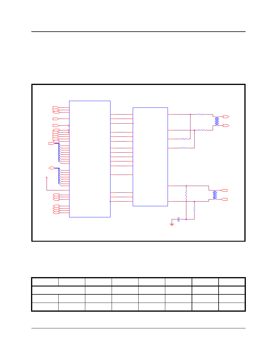
·Á
·Á
·Á
·Á
DS3/E3 FRAMER IC
XRT7250
REV. 1.1.1
123
The Line Interface and Scan Section of the XRT7250
DS3/E3 Framer IC consists of 5 output pins, 3 input
pins, a Read/Write register, and a Read-Only register.
The purpose of the Line Interface Drive and Scan
section is to permit the user to monitor and exercise
control over many aspects of the XRT7300 DS3/E3/
STS-1 LIU IC without having to develop the neces-
sary off-chip glue-logic.
Figure 39 presents a simple circuit schematic that de-
picts how the XRT7250 DS3/E3 Framer IC could be
interfaced to the XRT7300 DS3/E3/STS-1 LIU IC.
3.1
B
IT
-F
IELDS
WITHIN
THE
L
INE
I
NTERFACE
D
RIVE
R
EGISTER
As mentioned above, the Line Interface Drive and
Scan section consists of five output pins and three in-
put pins. The logic state of the output pins are con-
trolled by the contents within the Line Interface Drive
register, as depicted below.
The role of each of these bit-fields are their corre-
sponding output pins are depicted below.
F
IGURE
39. S
CHEMATIC
D
EPICTING
HOW
TO
INTERFACE
THE
XRT7250 DS3/E3 F
RAMER
IC
TO
THE
XRT7300 DS3/
E3/STS-1 LIU IC
5V
U1
XRT7250
TxPOS
65
TxNEG
64
TxLineClk
63
D M O
79
ExtLOS
78
RLOL
77
LLOOP
69
RLOOP
70
TAOS
68
TxLEV
67
ENCODIS
66
REQB
71
RxPOS
76
RxNEG
75
RxLineClk
74
MOTO
27
RESETB
28
A0
15
A1
16
A2
17
A3
18
A4
19
A5
20
A6
21
A7
22
A8
23
D0
32
D1
33
D2
34
D3
35
D4
36
D5
37
D6
38
D7
39
Rdy_Dtck
6
W R B _ R W
7
RDB_DS
10
CSB
8
ALE_AS
9
INTB
13
TxSER
46
TxInClk
43
TxFrame
61
RxSer
86
RxClk
88
RxFrame
90
RxLOS
95
RxOOF
94
RxRED
93
RxAIS
87
NIBBLEINTF
25
U2
XRT7300
TPDATA
37
TNDATA
38
TCLK
36
RCLK1
31
RNEG
32
RPOS
33
TTIP
41
TRING
40
MTIP
44
MRING
43
RRING
9
RTIP
8
D M O
4
RLOS
24
RLOL
23
LLB
14
RLB
15
TAOS
2
TxLEV
1
ENCODIS
21
REQDIS
12
T1
1:1
1
5
4
8
T2
1:1
1
5
4
8
R1
36
1
2
R2
36
1
2
R6
37.5
1
2
R3
270
1
2
R4
270
1
2
R5
37.5
1
2
C1
0.01uF
1
2
TxSER
TxInClk
NIBBLEINTF
RESETB
RTIP
RRING
CSB
R W
DS
AS
TxFrame
RxSer
RxClk
RxFrame
RxLOS
RxOOF
RxRED
RxAIS
A[8:0]
TRING
TTIP
INTB
D[7:0]
INTB
LINE INTERFACE DRIVE REGISTER (ADDRESS = 0X80)
B
IT
7
B
IT
6
B
IT
5
B
IT
4
B
IT
3
B
IT
2
B
IT
1
B
IT
0
Not Used
REQB
TAOS
ENCODIS
TXLEV
RLOOP
LLOOP
R/O
R/O
R/W
R/W
R/W
R/W
R/W
R/W
0
0
0
0
1
0
0
0

XRT7250
DS3/E3 FRAMER IC
·Á
·Á
·Á
·Á
REV. 1.1.1
124
Bit 5 - REQB - (Receive Equalization Enable/Dis-
able Select)
This Read/Write bit-field allows the user to control the
state of the REQB output pin of the Framer device.
This output pin is intended to be connected to the
REQB input pin of the XRT7300 DS3/E3/STS-1 LIU
IC. If the user forces this signal to toggle "High", then
the internal Receive Equalizer (within the XRT7300
device) will be disabled. Conversely, if the user forces
this signal to toggle "Low", then the Receive Equalizer
(within the XRT7300 device) will be enabled.
The purpose of the internal Receive Equalizer (within
the XRT7300 device) is to compensate for the Fre-
quency-Dependent attenuation (e.g., cable loss), that
a line signal will experience as it travels through coax-
ial cable, from the transmitting to the receiving termi-
nal.
Writing a "1" to this bit-field causes the Framer device
to toggle the REQB output pin "High". Writing a "0" to
this bit-field causes the Framer device to toggle the
REQB output pin "Low".
For information on the criteria that should be used
when deciding whether to enable or disable the Re-
ceive Equalizer, please consult the XRT7300 DS3/
E3/STS-1 LIU IC Data Sheet.
N
OTE
: If the customer is not using the XRT7300 DS3/E3/
STS-1 IC, then this bit-field and the REQB output pin can
be used for other purposes.
Bit 4 - TAOS - (Transmit All Ones Signal)
This Read/Write bit-field allows the user to control the
state of the TAOS output pin of the Framer device.
This output pin is intended to be connected to the
TAOS input pin of the XRT7300 DS3/E3/STS-1 LIU
IC. if the user forces this signal to toggle "High", then
the XRT7300 device will transmit an "All Ones" pat-
tern onto the line. Conversely, if the user commands
this output signal to toggle "Low" then the XRT7300
DS3/E3/STS-1 LIU IC will proceed to transmit data
based upon the data that it receives via the TxPOS
and TxNEG output pins (of the Framer IC).
Writing a "1" to this bit-field causes the TAOS output
pin to toggle "High". Writing a "0" to this bit-field will
cause this output pin to toggle "Low".
N
OTE
: If the customer is not using the XRT7300 DS3/E3/
STS-1 LIU IC, then this bit-field, and the TAOS output pin
can be used for other purposes.
Bit 3 - ENCODIS - (B3ZS/HDB3 Encoder Disable)
This Read/Write bit-field allows the user to control the
state of the ENCODIS output pin of the Framer de-
vice. This output pin is intended to be connected to
the ENCODIS input pin of the XRT7300 DS3/E3/
STS-1 LIU IC. If the user forces this signal to toggle
"High", then the internal B3ZS/HDB3 encoder (within
the XRT7300 device) will be disabled. Conversely, if
the user commands this output signal to toggle "Low",
then the internal B3ZS/HDB3 encoder (within the
XRT7300 device) will be enabled.
Writing a "1" to this bit-field causes the Framer IC to
toggle the Encodis output pin "High". Writing a "0" to
this bit-field will cause the Framer IC to toggle this
output pin "Low".
N
OTES
:
1. The B3ZS/HDB3 encoder, within the XRT7300
device is not to be confused with the B3ZS/HDB3
encoding capabilities that exists within the Transmit
DS3/E3 Framer block of the Framer IC.
2. The user is advised to disable the B3ZS/HDB3
encoder (within the XRT7300 IC) if the Transmit
and Receive DS3/E3 Framer (within the XRT7250)
are configured to operate in the B3ZS/HDB3 line
code.
3. If the customer is not using the XRT7300 DS3/E3/
STS-1 LIU IC, then this bit-field and the Encodis
output pin can be used for other purposes.
4. It is permissible to tie both the ENCODIS and
DECODIS input pins (of the XRT7300 device) to
the Encodis output pin of the XRT7250 DS3/E3
Framer IC.
Bit 2 - TxLEV (Transmit Line Build-Out Enable/
Disable Select)
This Read/Write bit-field allows the user to control the
state of the TxLEV output pin of the Framer device.
This output pin is intended to be connected to the Tx-
LEV input pin of the XRT7300 DS3/E3/STS-1 LIU IC.
Writing a "1" to this bit-field commands the Framer to
drive the TxLEV output pin "High".
Writing a "0" to this bit-field commands the Framer to
drive this output signal "Low".
If the user commands this signal to toggle "High",
then the Transmit Line Build-Out circuitry, within the
XRT7300 device will be disabled. In this mode, the
XRT7300 LIU IC will generate unshaped (e.g.,
square) pulses out onto the line, via the TTIP and
TRING output pins.
Conversely, if the user commands this signal to toggle
"Low", then the Transmit Line Build-Out circuitry, with-
in the XRT7300 device will be enabled. In this mode,
the XRT7300 device will generate shaped pulses on-
to the line, via the TTIP and TRING output pins.
In order to comply with the Isolated DSX-3 Pulse
Template requirements (per Bellcore GR-499-CORE),
the user is advised to set this bit-field to "0" if the ca-
ble length (between the transmit output of the
XRT7300 device and the DSX-3 Cross Connect Sys-
tem) is less than 225 feet. Conversely, the user is ad-

·Á
·Á
·Á
·Á
DS3/E3 FRAMER IC
XRT7250
REV. 1.1.1
125
vised to set this bit-field to "1" if the cable length (be-
tween the transmit output of the XRT7300 device and
the DSX-3 Cross Connect System) is greater than
225 feet.
N
OTE
: If the customer is not using the XRT7300 DS3/E3/
STS-1 IC, then this bit-field and the TxLEV output pin can
be used for other purposes.
Bit 1 - RLOOP (Remote Loop-Back Select)
This Read/Write bit-field permits the user to control
the state of the RLOOP output pin of the Framer de-
vice. This output pin is intended to be connected to
the RLOOP input pin of the XRT73001 LIU IC.
The state of this bit-field (or pin) along with LLOOP
are used to configure the XRT7300 device into one of
four (4) loop-back modes. The relationship of the val-
ues of RLOOP, LLOOP and the resulting loop-back
mode (within the XRT7300 device) is tabulated below.
Writing a "1" into this bit-field commands the Framer
to drive the RLOOP output signal "High". Writing a
"0" into this bit-field commands the Framer to drive
this output signal "Low".
For a detailed description of the XRT7300 LIU's oper-
ation during each of these loop-back modes, please
see the XRT7300 DS3/E3/STS-1 LIU IC data sheet.
N
OTE
: If the customer is not using the XRT7300 DS3/E3/
STS-1 LIU IC, then this bit-field and the RLOOP output pin
can be used for other purposes.
Bit 0 - LLOOP (Local Loop-back Select)
This Read/Write bit-field allows the user to control the
state of the LLOOP output pin of the Framer device.
This output pin is intended to be connected to the
LLOOP input pin of the XRT7300 DS3/E3/STS-1 LIU
IC.
The state of this bit-field (or pin) along with RLOOP
are used to configure the XRT7300 into one of four
(4) loop-back modes. The relationship of the values
of RLOOP, LLOOP and the resulting loop-back
modes (within the XRT7300 device) are presented in
Table 15.
Writing a "1" into this bit-field commands the Framer
to toggle the LLOOP output pin "High". Writing a "0"
into this bit-field commands the Framer to toggle this
output signal "Low".
For a detailed description of the XRT7300 LIU's oper-
ation during each of these loop-back modes, please
see the XRT7300 DS3/E3/STS-1 LIU IC Data Sheet.
N
OTE
: If the customer is not using the XRT7300 DS3/E3/
STS-1 LIU IC, then this bit-field and the LLOOP output pin
can be used for other purposes.
3.2
B
IT
-F
IELDS
WITHIN
THE
L
INE
I
NTERFACE
S
CAN
R
EGISTER
The XRT7300 device contains three output pins
which can be made accessible to the Microprocessor
Interface, via the Line Interface Scan register. These
three output pins are listed below.
∑ DMO - Drive Monitor Output
∑ RLOL - Receive Loss of Lock Indicator
∑ RLOS - Receive Loss of Signal Indicator.
The logic state of each of these input pins (or output
pins from the LIU) can be monitored by reading the
contents of the Line Interface Scan register, as de-
picted below.
T
ABLE
15: T
HE
R
ELATIONSHIP
BETWEEN
THE
STATES
OF
RLOOP, LLOOP
AND
THE
RESULTING
LOOP
-
BACK
MODE
WITH
THE
XRT7300
DEVICE
RLOOP
LLOOP
RESULTING LOOP-BACK MODE (WITHIN THE XRT7300 DS3/E3/STS-1 LIU IC)
0
0
Normal Mode (No Loop-back)
0
1
Analog Local Loop-back Mode
1
0
Remote Loop-back Mode
1
1
Digital Local Loop-back Mode

XRT7250
DS3/E3 FRAMER IC
·Á
·Á
·Á
·Á
REV. 1.1.1
126
The meaning/role of each of these bit-field and their
corresponding input pins are defined below.
Bit 2 - DMO - Drive Monitor Output
This Read-Only bit-field indicates the logic state of
the DMO output pin of the Framer device. This input
pin is intended to be connected to the DMO output
pin of the XRT7300 DS3/E3/STS-1 LIU IC. If this bit-
field contains a logic "1", then the DMO input pin is
"High". The XRT7300 DS3/E3/STS-1 LIU IC will set
this pin "High" if the Transmit Driver Monitor circuitry
(within the XRT7300 device) has not detected any bi-
polar signals at the MTIP and MRING inputs (of the
XRT7300 device) within the last 128 + 32 bit periods.
Conversely, if this bit-field is set to "0", then the DMO
input pin is "Low". The XRT7300 DS3/E3/STS-1 LIU
IC will set this pin "Low" if bipolar signals are being
detected at the MTIP and MRING input pins.
For more information on the user/purpose of the
Drive Monitor feature, within the XRT7300 LIU IC,
please see the XRT7300 DS3/E3/STS-1 LIU IC Data
Sheet.
N
OTE
: If this customer is not using the XRT7300 DS3/E3/
STS-1 LIU IC, then this register bit-field and input pin can
be used for a variety of other purposes.
Bit 1 - RLOL - Receive Loss of Lock
This Read-Only bit-field indicates the logic state of
the RLOL input pin of the Framer device. This input
pin is intended to be connected to the RLOL output
pin of the XRT7300 DS3/E3/STS-1 LIU IC. If this bit-
field contains a logic "1", then the RLOL input pin is
"High". The XRT7300 LIU IC will drive this pin "High"
if the clock recovery phase locked loop circuitry (with-
in the XRT7300 device) has lost lock with the incom-
ing DS3 or E3 data-stream and is not properly recov-
ering clock and data.
Conversely, if this bit-field contains a logic "0", then
the RLOL input pin is "Low". The XRT7300 DS3/E3/
STS-1 LIU IC will hold this pin "Low" for as long as
this clock recovery phase-locked-loop circuit (within
the XRT7300 device) is properly locked onto the in-
coming DS3 or E3 data stream and is properly recov-
ering clock and data from this data stream.
Bit 0 - RLOS- Receive Loss of Signal
This Read-Only bit-field indicates the logic state of
the RLOS input pin of the Framer device. This input
pin is intended to be connected to the RLOS output
pin of the XRT7300 DS3/E3/STS-1 LIU IC. If this bit-
field contains a logic "1", then the RLOS input pin is
"High". The XRT7300 LIU IC will drive this signal
"High" if it is currently declaring an LOS (Loss of Sig-
nal) condition.
Conversely, if this bit-field contains a logic "0", then
the RLOS input pin is "Low". The XRT7300 LIU IC
will drive this signal "Low", if it is NOT currently de-
claring an LOS (Loss of Signal) condition.
For more information on the LOS Declaration/Clear-
ance criteria, used by the XRT7300 device, please
see the XRT7300 DS3/E3/STS-1 LIU IC Data Sheet.
N
OTE
: Asserting the RLOS input pin will cause the Framer
device to generate a Change in LOS Condition interrupt
and declare an LOS (Loss of Signal) condition to the Micro-
processor/Microcontroller. Therefore, the user is not
advised to use the RLOS input pin as a General Purpose
Input pin.
LINE INTERFACE SCAN REGISTER (ADDRESS = 0X81)
B
IT
7
B
IT
6
B
IT
5
B
IT
4
B
IT
3
B
IT
2
B
IT
1
B
IT
0
Not Used
DMO
RLOL
RLOS
R/O
R/O
R/O
R/O
R/O
R/O
R/O
R/O
0
0
0
0
0
0
0
0
·Á
·Á
·Á
·Á
DS3/E3 FRAMER IC
XRT7250
REV. 1.1.1
127
XRT7250 CONFIGURATION
The XRT7250 DS3/E3 Framer IC can be configured
to support any of the following four framing formats.
∑ DS3/C-Bit Parity
∑ DS3/M13
∑ E3/ITU-T G.832
∑ E3/ITU-T G.751
As a consequence, the discussion of the XRT7250
Framer IC will be organized as follows:
Section 4.0 - DS3 Mode Operation of the XRT7250
Section 5.0 - E3, ITU-T G.751 Operation of the
XRT7250
Section 6.0 - E3, ITU-T G.832 Operation of the
XRT7250
Section 6.0 - Framer Local Loop-back Mode Opera-
tion
4.0
DS3 OPERATION OF THE XRT7250
This section will discuss in detail, the operation of the
XRT7250 Framer IC, when it has been configured to
operate in the DS3 Mode.
Configuring the XRT7250 to Operate in the DS3
Mode
The XRT7250 can be configured to operate in the
DS3 Mode by writing a "1" into bit-field 6 within the
Framer Operating Mode register, as illustrated below.
Prior to describing the functional blocks within the
Transmit and Receive Sections of the XRT7250, it is
important to describe the following two framing for-
mats.
∑ M13
∑ C-Bit Parity
4.1
D
ESCRIPTION
OF
THE
DS3 F
RAMES
AND
A
SSOCI
-
ATED
O
VERHEAD
B
ITS
The role of the various overhead bits are best de-
scribed by discussing the DS3 Frame Format as a
whole. The DS3 Frame contains 4760 bits, of which
56 bits are overhead and the remaining 4704 bits are
payload bits. The payload data is formatted into
packets of 84 bits and the overhead (OH) bits are in-
serted between these payload packets. The
XRT7250 Framer supports the following two DS3
framing formats:
∑ C-bit Parity
∑ M13
Figures 40 and 41 present the DS3 Frame Format for
C-bit Parity and M13, respectively.
X = Signaling bit for network control
I = Payload Information (84 bit packets)
FRAMER OPERATING MODE REGISTER (ADDRESS = 0X00)
B
IT
7
B
IT
6
B
IT
5
B
IT
4
B
IT
3
B
IT
2
B
IT
1
B
IT
0
Local Loopback
DS3/E3*
Internal LOS
Enable
RESET
Interrupt
Enable Reset
Frame Format
TimRefSel[1:0]
R/W
R/W
R/W
R/W
R/W
R/W
R/W
R/W
x
1
x
0
x
x
x
x
F
IGURE
40. DS3 F
RAME
F
ORMAT
FOR
C-
BIT
P
ARITY
X
I
F1
I
AIC
I
F0
I
NA
I
F0
I
FEAC
I
F1
I
I
X
I
F1
I
UDL
I
F0
I
NA
I
F0
I
UDL
I
F1
I
P
I
F1
I
CP
I
F0
I
CP
I
F0
I
CP
I
F1
I
P
I
F1
I
FEBE
I
F0
I
FEBE
I
F0
I
FEBE
I
F1
I
M0
I
F1
I
DL
I
F0
I
DL
I
F0
I
DL
I
F1
I
M1
I
F1
I
UDL
I
F0
I
UDL
I
F0
I
UDL
I
F1
I
M0
I
F1
I
UDL
I
F0
I
UDL
I
F0
I
UDL
I
F1
I
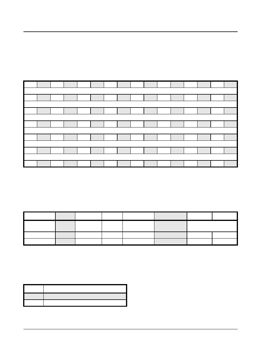
XRT7250
DS3/E3 FRAMER IC
·Á
·Á
·Á
·Á
REV. 1.1.1
128
Fi = Frame synchronization bit with logic value i
P = Parity bit
Mi = Multiframe synchronization bit with logic value i
AIC = Application Identification Channel
NA = reserved for network application
FEAC = Far End Alarm and Control
DL = Data Link
CP = CP (Path)-bit parity
FEBE = Far End Block Error
UDL = User Data Link
X = Signaling bit for network control
I = Payload Information (84 bit packets)
Fi = Frame synchronization bit with logic value i
Cij = jth stuff code bit of ith channel
P = Parity bit
Mi = multiframe synchronization bit with logic values i
The user can choose between these two frame for-
mats, by writing the appropriate data to bit 2 of the
Framer Operating Mode Register (Address = 0x00),
as depicted below.
Table 16 lists the relationship between the value of
the this bit-field and the resulting DS3 Frame Format.
N
OTE
: This bit setting also configures the frame format for
both the Transmit and Receive Section of the XRT7250.
Each of the two DS3 Frame Formats, as presented in
Figure 40 and Figure 41, constitute an M-frame (or a
full DS3 Frame). Each M-frame consists of 7 - 680 bit
F-frames (sometimes referred to as, subframes). In
Figure 40 and 41, each F-frame is represented by
the individual rows of payload and overhead bits.
Each F-frame can be further divided into 8 blocks of
85 bits, with 84 of the 85 bits available for payload in-
formation and the remaining one bit used for frame
overhead.
Differences Between the M13 and C-Bit Parity
Frame Formats
The frame formats for M13 and C-bit Parity are very
similar. However, the main difference between these
F
IGURE
41. DS3 F
RAME
F
ORMAT
FOR
M13
X
I
F1
I
C11
I
F0
I
C12
I
F0
I
C13
I
F1
I
I
X
I
F1
I
C21
I
F0
I
C22
I
F0
I
C23
I
F1
I
P
I
F1
I
C31
I
F0
I
C32
I
F0
I
C33
I
F1
I
P
I
F1
I
C41
I
F0
I
C42
I
F0
I
C43
I
F1
I
M0
I
F1
I
C51
I
F0
I
C52
I
F0
I
C53
I
F1
I
M1
I
F1
I
C61
I
F0
I
C62
I
F0
I
C63
I
F1
I
M0
I
F1
I
C71
I
F0
I
C72
I
F0
I
C73
I
F1
I
FRAMER OPERATING MODE REGISTER (ADDRESS = 0X00)
B
IT
7
B
IT
6
B
IT
5
B
IT
4
B
IT
3
B
IT
2
B
IT
1
B
IT
0
Local Loopback
DS3/E3*
Internal LOS
Enable
RESET
Interrupt
Enable Reset
Frame Format
TimRefSel[1:0]
R/W
R/W
R/W
R/W
R/W
R/W
R/W
R/W
x
1
x
0
x
x
x
x
T
ABLE
16: T
HE
R
ELATIONSHIP
BETWEEN
THE
CONTENT
OF
B
IT
2, (C-B
IT
P
ARITY
*/M13)
WITHIN
THE
F
RAMER
O
PERATING
M
ODE
R
EGISTER
AND
THE
RESULTING
DS3
F
RAMING
F
ORMAT
B
IT
2
DS3 F
RAME
F
ORMAT
0
C-Bit Parity
1
M13

·Á
·Á
·Á
·Á
DS3/E3 FRAMER IC
XRT7250
REV. 1.1.1
129
two framing formats is in the use of the C-bits. In the
M13 Format, the C-bits reflect the status of stuff-op-
portunities that either were or were not used while
multiplexing the 7 DS2 signals into this DS3 signal. If
two of the three stuff bits, within a F-frame, are "1",
then the associated stuff bit, Si (not shown in
Figure 41), is interpreted as being a stuff bit. In the
C-bit Parity framing format, the C bits take on different
roles, as presented in Table 17.
Definition of the DS3 Frame Overhead Bits
In general, the DS3 Frame Overhead Bits serve the
following three purposes:
1. Support Frame Synchronization between the
Local and Remote DS3 Terminals
2. Provide parity bits in order to facilitate perfor-
mance monitoring and error detection.
3. Support the transmission of Alarms, Status, and
Data Link information to the Remote DS3 Termi-
nal.
The Overhead bits supporting each of these purpos-
es are further defined below.
4.1.1
Frame Synchronization Bits (Applies to
both M13 and C-bit Parity Framing Formats)
Each DS3 Frame (M-frame) contains a total of 31 bits
that support frame synchronization. Each DS3 M-
frame contains three M-bits. According to Figure 40
and Figure 41, these M-bits are the first bits in F-
frames 5, 6 and 7. These three bits appear in each
M-frame with the repeating pattern of "010". This fact
is also presented in Figure 40 and Figure 41, which
contains bit-fields that are designated as: M0, M1,
and M0 (where M0 = "0", and M1 = "1").
Each F-frame contains four F-bits, which also aid in
synchronization between the Local and the remote
DS3 terminals. Therefore, each DS3 M-frame con-
sists of a total of 28 F-bits. These F-bits exhibit a re-
peating pattern of "1001" within each F-frame. This
fact is also presented in Figure 40 and Figure 41,
which contains bit-fields that are designated as: F1,
F0, F0, and F1 (where F0 = "0", and F1 = "1").
Each of these bit-fields will be used by the Receive
DS3 Framer block, within the remote terminal equip-
ment, to perform Frame Acquisition and Frame Main-
tenance functions.
N
OTE
: For more information on how the Receive DS3
Framer uses these bit-fields, please see Section 3.3.2.
4.1.2
Performance Monitoring/Error Detection
Bits (Parity)
The DS3 Frame uses numerous bit fields to support
performance monitoring of the transmission link be-
tween the Local Transmitting Terminal and the Re-
mote Receiving Terminal. The DS3 frame can con-
tain two types of parity bits, depending upon the fram-
ing format chosen. P-bits are available in both the
M13 and C-bit Parity Formats. However, the C-bit
Parity format also includes additional CP-Parity bits.
P-Bits (Applies to M13 and C-Bit Parity Frame For-
mats)
Each DS3 M-frame consists of two (2) P-bits. These
two P-bits carry the parity information of the previous
DS3 frame for performance monitoring. These two P-
bits must be identical, within a given DS3 frame. The
Transmit Section will compute the even parity over all
4704 payload bits within a given DS3 frame, and in-
sert the resulting parity information in the P-bit fields
of the very next DS3 frame. The two P-bits are set to
"1" if the payload of the previous DS3 frame consists
of an odd number of "ones" in the frame. Conversely,
T
ABLE
17: C-
BIT
F
UNCTIONS
FOR
THE
C-
BIT
P
ARITY
DS3 F
RAME
F
ORMAT
C - B
IT
F
UNCTION
OF
C-
BITS
WHILE
IN
THE
C-B
IT
P
ARITY
F
RAMING
F
ORMAT
C11
AIC (C-Bit Parity Mode)
C12
NA (Reserved for Network Application)
C13
FEAC (Far End Alarm & Control)
C21, C22, C23
(UDL) User Data Link (undefined for DS3 Frame)
C31,C32, C33
CP (Path) Parity Bits
C41, C42, C43
FEBE (Far End Block Error) Indicators
C51, C52, C53
(DL) Path Maintenance Data Link
C61, C62, C63,
C71, C72, C73
(UDL) User Data Link (undefined for DS3 Frame)

XRT7250
DS3/E3 FRAMER IC
·Á
·Á
·Á
·Á
REV. 1.1.1
130
the two P-bits are set to zero if an even number of
"ones" is found in the payload of the previous DS3
frame. For information on how the Receive DS3
Framer handles P-bits, please see Section 3.3.2.6.1.
CP-(Path) Parity Bits (Applies to only the C-Bit
Parity Framing Format)
Each DS3 M-Frame consists of tw0 (2) CP-Bits.
These two bits have a very similar role to those of P-
Bits. Further, the XRT7250 Framer IC processes CP-
Bits in an identical manner that it handles P-Bits.
However for some DS3 applications, there is a differ-
ence between P and CP-bits, that should be noted.
∑ P-Bits are used to support error detection of a DS3
data stream as it travels from one T.E. to the next.
(e.g., a single DS3 link between two T.E.)
∑ CP-Bits are used to support error detection of DS3
data stream as it travels from the Source T.E.
(where the DS3 Data Stream originated), to the
Sink T.E, (where the DS3 Data Stream is termi-
nated.)
N
OTE
: This transmission path from Source T.E. to Sink T.E.
may involve numerous T.E.
∑ P-Bits are verified and recomputed as it passes
through a Mid-Network T.E. (which is neither a
Source nor Sink T.E.)
∑ The values of the CP-Bits (as generated by the
Source T.E.) must be preserved as a DS3 frame
travels to the Sink T.E. (Through any number of
Mid-Network T.E.)
For more information on how CP-Bits are processed,
please see section 3.3.2.6.2
4.1.3
Alarm and Signaling-Related Overhead
Bits
The DS3 frame consists of mumerous bit-fields which
are used to support the handling of alarm and signal-
ing information. Each of these bit-fields are defined
below.
The Alarm Indication Signal (AIS) Pattern (C-Bit
Parity Framing Format only)
The Alarm Indication Signal (AIS) pattern is an alarm
signal that is inserted into the outbound DS3 stream
when a failure is detected by the Local Terminal. The
Transmit DS3 Framer will generate the AIS pattern as
defined in ANSI.T1.107a-1990, which is described as
follows.
V
ALID
M-
BITS
, F-
BITS
,
AND
P-
BITS
∑ All C-bits are zeros
∑ All X-bits are set to "1"
∑ A repeating "1010..." pattern is written into the pay-
load of the DS3 frames.
Consequently, no user (or payload) data will be trans-
mitted while the Transmit Section of the chip is trans-
mitting the AIS pattern.
The IDLE Condition Signal
The IDLE Condition signal is used to indicate that the
DS3 channel is functionally sound, but has not yet
been assigned any traffic. The Transmit Section will
transmit the IDLE Condition signal as defined in ANSI
T1.107a-1990, which is described as follows.
∑ Valid M-bits, F-bits, and P-bits
∑ The three CP-bits (F-frame #3) are zeros
∑ The X-bits are set to "1"
∑ A repeating "1100.." pattern is written into the pay-
load of the DS3 frames.
FEAC - Far End Alarm & Control (Only available
for the C-bit Parity Frame Format)
The third C-bit (C13 or FEAC) in the first F-frame is
used as the Far End Alarm and Control (FEAC) chan-
nel between the Near-End DS3 terminal and the Re-
mote DS3 terminal. The FEAC channel carries:
∑ Alarm and Status Information
∑ Loopback commands to initiate and deactivate DS3
and DS1 loopbacks at the distant terminals.
The FEAC message consists of a six (6) bit code
word of the form [d5, d4, d3, d2, d1 d0]. This mes-
sage is encapsulated with 10 framing bits to form a
16 bit FEAC Message, as illustrated below. The
FEAC signals are encoded into repeating 16 bit mes-
sage of the form:
Since each DS3 frame carries only one FEAC bit, 16
DS3 frames are required to deliver 1 complete FEAC
message. The six bits labeled "dx" can represent up-
to 64 distinct messages, of which 43 have been de-
fined in the standards. For a more detailed discus-
sion on the transmission of FEAC Messages, please
see Section 3.2.3.1.
FEBE - Far End Block Error (Only available for the
C-bit Parity Frame Format)
F-Frame # 4 consists of 3 bit fields for the FEBE (Far-
End Block Error) channel. If the (Local) Receive Sec-
tion (within the Framer IC) detects P-bit parity errors,
CP-bit errors or a framing error on the incoming (re-
ceived) DS3 stream it will inform the Transmit Section
of this fact. The Transmit Section will, in turn, set the
0
d5
d4
d3
d2
d1
d0
0
1
1
1
1
1
1
1
1

·Á
·Á
·Á
·Á
DS3/E3 FRAMER IC
XRT7250
REV. 1.1.1
131
three FEBE bits (within an outgoing DS3 Frame) to
any pattern other than "111" to indicate an error. The
Transmit Section will then transmit this information
out to the Remote Terminal (e.g., the source of the er-
rored-data). The FEBE bits, in the outbound DS3
frames, are set to "111" only if both of the following
conditions are true:
∑ The Receive DS3 Framer has detected no M-bit or
F-bit framing errors, and
∑ No P-Bit parity errors have been detected.
∑ No CP-Bit errors have been detected.
N
OTE
: A more detailed discussion on the Transmit Sec-
tion's handling of the FEBE bit-fields can be found in Sec-
tion 3.2.4.2.1.9.
The Yellow Alarm or FERF (Far-End Receive Fail-
ure) Indicator
The X-bits are used for sending Yellow Alarms or the
FERF (Far-End Receive Failure) indication. When
the Receive Section (of the XRT7250), within the Re-
mote Receiving terminal equipment, cannot identify
valid framing, or detects an AIS pattern in the incom-
ing DS3 data-stream, the Framer IC can be config-
ured such that the Transmit Section will send a Yellow
Alarm or a FERF (Far-End Receive Failure) indication
to the Remote Terminal by setting both of the X-bits to
zero in the outbound (returning) DS3 path. The X-
bits are set to "1" during non-alarm conditions.
4.1.4
The Data Link Related Overhead Bits
UDL: User Data Link (C-bit Parity Frame Format
Only)
These bit-fields are not used by the framer and are
set to "1" by default. However, these bits may be
used for the transmission of data via a proprietary da-
ta link. The user can access these bit-fields via the
Transmit Overhead Data Input Interface and the Re-
ceive Overhead Data Output Interface blocks.
DL: Path Maintenance Data Link (C-bit Parity
Frame Format Only)
The LAPD transceiver block uses these bit-fields for
the transmission and reception of path maintenance
data link (PMDL) messages via ITU-T Q.921 (LAP-D)
Message frames. Please see Sections 3.2.3.2 and
3.3.3.2 for more information on the operation and
function of the LAPD Transmitter.
4.2
T
HE
T
RANSMIT
S
ECTION
OF
THE
XRT7250 (DS3
M
ODE
O
PERATION
)
When the XRT7250 has been configured to operate
in the DS3 Mode, the Transmit Section of the
XRT7250 consists of the following functional blocks.
∑ Transmit Payload Data Input Interface block
∑ Transmit Overhead Data Input Interface block
∑ Transmit DS3 Framer block
∑ Transmit DS3 HDLC Controller block
∑ Transmit LIU Interface block
Figure 42 presents a simple illustration of the Trans-
mit Section of the XRT7250 Framer IC.

XRT7250
DS3/E3 FRAMER IC
·Á
·Á
·Á
·Á
REV. 1.1.1
132
Each of these functional blocks will be discussed in
detail in this document.
4.2.1
The Transmit Payload Data Input Interface
Block
Figure 43 presents a simple illustration of the Trans-
mit Payload Data Input Interface block.
F
IGURE
42. A S
IMPLE
I
LLUSTRATION
OF
THE
T
RANSMIT
S
ECTION
,
WITHIN
THE
XRT7250,
WHEN
IT
HAS
BEEN
CON
-
FIGURED
TO
OPERATE
IN
THE
DS3 M
ODE
Transmit
Payload Data
Input
Interface Block
Transmit DS3/E3
Framer Block
Transmit LIU
Interface
Block
TxSer
TxNib[3:0]
TxInClk
TxPOS
TxNEG
TxLineClk
Transmit Overhead
Input
Interface Block
TxOHClk
TxOHIns
TxOHInd
TxOH
TxOHEnable
TxOHFrame
TxNibClk
TxFrame
Tx DS3 HDLC
Controller/Buffer
Tx DS3 HDLC
Controller/Buffer
From Microprocessor
Interface Block

·Á
·Á
·Á
·Á
DS3/E3 FRAMER IC
XRT7250
REV. 1.1.1
133
Each of the input and output pins of the Transmit Pay-
load Data Input Interface are listed in Table 18 and
described below. The exact role that each of these
inputs and output pins assume, for a variety of operat-
ing scenarios, are described throughout this section.
F
IGURE
43. A S
IMPLE
I
LLUSTRATION
OF
THE
T
RANSMIT
P
AYLOAD
D
ATA
I
NPUT
I
NTERFACE
B
LOCK
Transmit Payload
Data Input
Interface Block
Transmit Payload
Data Input
Interface Block
TxOH_Ind
TxSer
TxNib[3:0]
TxInClk
TxNibClk
TxFrame
TxFrameRef
To Transmit DS3 Framer Block

XRT7250
DS3/E3 FRAMER IC
·Á
·Á
·Á
·Á
REV. 1.1.1
134
T
ABLE
18: L
ISTING
AND
D
ESCRIPTION
OF
THE
PINS
ASSOCIATED
WITH
THE
T
RANSMIT
P
AYLOAD
D
ATA
I
NPUT
I
NTERFACE
S
IGNAL
N
AME
T
YPE
D
ESCRIPTION
TxSer
Input
Transmit Serial Payload Data Input Pin:
If the user opts to operate the XRT7250 in the serial mode, then the Terminal Equipment is
expected to apply the payload data (that is to be transported via the outbound DS3 data
stream) to this input pin. The XRT7250 will sample the data that is at this input pin upon the
rising edge either the RxOutClk or the TxInClk signal (whichever is appropriate).
N
OTE
: This signal is only active if the NibInt input pin is pulled "Low".
TxNib[3:0]
Input
Transmit Nibble-Parallel Payload Data Input pins:
If the user opts to operate the XRT7250 in the Nibble-Parallel mode, then the Terminal Equip-
ment is expected to apply the payload data (that is to be transported via the outbound DS3
data stream) to these input pins. The XRT7250 will sample the data that is at these input pins
upon the rising edge of the TxNibClk signal.
N
OTE
: These pins are only active if the NibInt input pin is pulled "High".
TxNibFrame
Output Transmit End of Frame Output Indicator - Nibble Mode
The Transmit Section of the XRT7250 will pulse this output pin "High" (for one nibble-period),
when the Transmit Payload Data Input Interface is processing the last nibble of a given DS3
frame.
The purpose of this output pin is to alert the Terminal Equipment that it needs to begin trans-
mission of a new DS3 frame to the XRT7250.
TxInClk
Input
Transmit Section Timing Reference Clock Input pin:
The Transmit Section of the XRT7250 can be configured to use this clock signal as the Timing
Reference. If the user has made this configuration selection, then the XRT7250 will use this
clock signal to sample the data on the TxSer input pin.
N
OTE
: If this configuration has been selected, then a 44.736 MHz clock signal must be applied
to this input pin.
TxNibClk
Output Transmit Nibble Mode Output
If the user opts to operate the XRT7250 in the Nibble-Parallel mode, then the XRT7250 will
derive this clock signal from the selected Timing Reference for the Transmit Section of the chip
(e.g., either the TxInClk or the RxLineClk signals).
The user is advised to configure the Terminal Equipment to output the outbound payload data
(to the XRT7250 Framer IC) onto the TxNib[3:0] input pins, upon the rising edge of this clock
signal.
N
OTE
: For DS3 Applications, the XRT7250 Framer IC will output 1176 clock edges (to the Ter-
minal Equipment) for each outbound DS3 frame.
TxOHInd
Output Transmit Overhead Bit Indicator Output:
This output pin will pulse "High" one-bit period prior to the time that the Transmit Section of the
XRT7250 will be processing an Overhead bit. The purpose of this output pin is to warn the
Terminal Equipment that, during the very next bit-period, the XRT7250 is going to be process-
ing an Overhead bit and will be ignoring any data that is applied to the TxSer input pin.
For DS3 applications, this output pin is only active if the XRT7250 is operating in the Serial
Mode. This output pin will be pulled "Low" if the device is operating in the Nibble-Parallel
Mode.
TxFrame
Output Transmit End of Frame Output Indicator:
The Transmit Section of the XRT7250 will pulse this output pin "High" (for one bit-period),
when the Transmit Payload Data Input Interface is processing the last bit of a given DS3 frame.
The purpose of this output pin is to alert the Terminal Equipment that it needs to begin trans-
mission of a new DS3 frame to the XRT7250 (e.g., to permit the XRT7250 to maintain Transmit
DS3 framing alignment control over the Terminal Equipment).

·Á
·Á
·Á
·Á
DS3/E3 FRAMER IC
XRT7250
REV. 1.1.1
135
Operation of the Transmit Payload Data Input In-
terface
The Transmit Payload Data Input Interface is ex-
tremely flexible, in that it permits the user to make the
following configuration options.
∑ The Serial or the Nibble-Parallel Interface Mode
∑ The Loop-Timing or the TxInClk (Local Timing)
Mode
Further, if the XRT7250 has been configured to oper-
ate in the TxInClk (Local Timing) mode, then the user
has two additional options.
∑ The XRT7250 functions as the Frame Master (e.g.,
it dictates when the Terminal Equipment will initiate
the transmission of data within a new DS3 frame).
∑ The XRT7250 functions as the Frame Slave (e.g.,
the Terminal Equipment will dictate when the
XRT7250 initiates the transmission of a new DS3
frame).
Given these three set of options, the Transmit Termi-
nal Input Interface can be configured to operate in
one of the six (6) following modes.
∑ Mode 1 - Serial/Loop-Timed Mode
∑ Mode 2 - Serial/Local-Timed/Frame Slave Mode
∑ Mode 3 - Serial/Local-Timed/Frame Master Mode
∑ Mode 4 - Nibble/Loop-Timed Mode
∑ Mode 5 - Nibble/Local-Timed/Frame Slave Mode
∑ Mode 6 - Nibble/Local-Timed/Frame Master Mode
Each of these modes are described, in detail, below.
4.2.1.1
Mode 1 - The Serial/Loop-Timing Mode
The Behavior of the XRT7250
If the XRT7250 has been configured to operate in this
mode, then the XRT7250 will behave as follows.
A. Loop-Timing (Uses the RxLineClk signal as the
Timing Reference)
Since the XRT7250 is configured to operate in the
loop-timed mode, the Transmit Section (of the
XRT7250) will use the RxLineClk input clock signal
(e.g., the Recovered Clock signal, from the LIU) as its
timing source. When the XRT7250 is operating in
this mode it will do the following.
1. It will ignore any signal at the TxInClk input pin.
2. The XRT7250 will output a 44.736MHz clock sig-
nal via the RxOutClk output pin. This clock signal
functions as the Transmit Payload Data Input
Interface block clock signal.
3. The XRT7250 will use the rising edge of the
RxOutClk signal to latch in the data residing on
the TxSer input pin.
B. Serial Mode
The XRT7250 will accept the DS3 payload data from
the Terminal Equipment, in a serial-manner, via the
TxSer input pin The Transmit Payload Data Input In-
terface block will latch this data into its circuitry, on the
rising edge of the RxOutClk output clock signal.
C. Delineation of outbound DS3 frames
The XRT7250 will pulse the TxFrame output pin
"High" for one bit-period coincident with the XRT7250
processing the last bit of a given DS3 frame.
D. Sampling of Payload Data, from the Terminal
Equipment
In Mode 1, the XRT7250 will sample the data at the
TxSer input, on the rising edge of RxOutClk.
Interfacing the Transmit Payload Data Input Inter-
face block (of the XRT7250) to the Terminal Equip-
ment for Mode 1 Operation
TxFrameRef
Input
Transmit Frame Reference Input:
The XRT7250 permits the user to configure the Transmit Section to use this input pin as a
frame reference. If the user makes this configuration selection, then the Transmit Section will
initiate its transmission of a new DS3 frame, upon the rising edge of this signal.
The purpose of this input pin is to permit the Terminal Equipment to maintain Transmit DS3
Framing alignment control over the XRT7250.
RxOutClk
Output Loop-Timed Timing Reference Clock Output pin:
The Transmit Section of the XRT7250 can be configured to use the RxLineClk signal as the
Timing Reference (e.g., loop-timing). If the user has made this configuration selection, then
the XRT7250 will:
∑
Output a 44.736 MHz clock signal via this pin, to the Terminal Equipment.
∑
Sample the data on the TxSer input pin, upon the rising edge of this clock signal.
T
ABLE
18: L
ISTING
AND
D
ESCRIPTION
OF
THE
PINS
ASSOCIATED
WITH
THE
T
RANSMIT
P
AYLOAD
D
ATA
I
NPUT
I
NTERFACE
S
IGNAL
N
AME
T
YPE
D
ESCRIPTION

XRT7250
DS3/E3 FRAMER IC
·Á
·Á
·Á
·Á
REV. 1.1.1
136
Figure 44 presents an illustration of the Transmit Pay-
load Data Input Interface block (within the XRT7250)
being interfaced to the Terminal Equipment, for Mode
1 operation.
Mode 1, Operation of the Terminal Equipment
When the XRT7250 is operating in this mode, it will
function as the source of the 44.736MHz clock signal
(via the RxOutClk signal). This clock signal will be
used as the Terminal Equipment Interface clock by
both the XRT7250 IC and the Terminal Equipment.
The Terminal Equipment will serially output the pay-
load data of the outbound DS3 data stream via its
DS3_Data_Out pin. The Terminal Equipment will up-
date the data on the DS3_Data_Out pin upon the ris-
ing edge of the 44.736 MHz clock signal, at its
DS3_Clock_In input pin (as depicted in Figure 44 and
Figure 45).
The XRT7250 will latch the outbound DS3 data
stream (from the Terminal Equipment) on the rising
edge of the RxOutClk signal.
The XRT7250 will indicate that it is processing the
last bit, within a given outbound DS3 frame, by puls-
ing its TxFrame output pin "High" for one bit-period.
When the Terminal Equipment detects this pulse at its
Tx_Start_of_Frame input, it is expected to begin
transmission of the very next outbound DS3 frame to
the XRT7250 via the DS3_Data_Out (or TxSer pin).
Finally, the XRT7250 will indicate that it is about to
process an overhead bit by pulsing the TxOH_Ind
output pin "High" one bit period prior to its processing
of an OH (Overhead) bit. In Figure 44, the TxOH_Ind
output pin is connected to the DS3_Overhead_Ind in-
put pin of the Terminal Equipment. Whenever the
DS3_Overhead_Ind pin is pulsed "High" the Terminal
Equipment is expected to not transmit a DS3 payload
bit upon the very next clock edge. Instead, the Termi-
nal Equipment is expected to delay its transmission of
the very next payload bit, by one clock cycle.
The behavior of the signals, between the XRT7250
and the Terminal Equipment, for DS3 Mode 1 opera-
tion is illustrated in Figure 45.
F
IGURE
44. I
LLUSTRATION
OF
THE
T
ERMINAL
E
QUIPMENT
BEING
INTERFACED
TO
THE
T
RANSMIT
P
AYLOAD
D
ATA
I
NPUT
I
NTERFACE
BLOCK
(
OF
THE
XRT7250)
FOR
M
ODE
1(S
ERIAL
/L
OOP
-T
IMING
) O
PERATION
Terminal Equipment
XRT7250 DS3 Framer
DS3_Data_Out
DS3_Clock_In
Tx_Start_of_Frame
DS3_Overhead_Ind
TxSer
RxOutClk
TxFrame
TxOH_Ind
NibInt
44.736 MHz

·Á
·Á
·Á
·Á
DS3/E3 FRAMER IC
XRT7250
REV. 1.1.1
137
.
How to configure the XRT7250 into the Serial/
Loop-Timed/Non-Overhead Interface Mode
1. Set the NibIntf input pin "Low".
2. Set the TimRefSel[1:0] bit fields (within the
Framer Operating Mode Register) to "00", as
illustrated below.
3. Interface the XRT7250, to the Terminal Equip-
ment, as illustrated in Figure 44.
N
OTE
: The XRT7250 Framer IC cannot support the Framer
Local Loop-back Mode of operation, when operating in the
Loop-Timing Mode. The user must configure the XRT7250
Framer IC into any of the following modes, prior to configur-
ing the Framer Local Loop-back Mode.
∑ Mode 2 - Serial/Local-Timed/Frame-Slave Mode.
∑ Mode 3 - Serial/Local-Timed/Frame-Master Mode.
∑ Mode 5 - Nibble-Parallel/Local-Timed/Frame-Slave
Mode.
∑ Mode 6 - Nibble-Parallel/Local-Timed/Frame-Mas-
ter Mode.
For more detailed information on Framer Local Loop-
back Mode of operation, please see Section 6.0.
4.2.1.2
Mode 2 - The Serial/Local-Timed/
Frame-Slave Mode Behavior of the XRT7250
If the XRT7250 has been configured to operate in this
mode, then the XRT7250 will function as follows.
A. Local-Timing - Uses the TxInClk signal as the
Timing Reference
In this mode, the Transmit Section of the XRT7250
will use the TxInClk signal as its timing reference.
B. Serial Mode
F
IGURE
45. B
EHAVIOR
OF
THE
T
ERMINAL
I
NTERFACE
SIGNALS
BETWEEN
THE
T
RANSMIT
P
AYLOAD
D
ATA
I
NPUT
I
NTERFACE
BLOCK
OF
THE
XRT7250
AND
THE
T
ERMINAL
E
QUIPMENT
(
FOR
M
ODE
1 O
PERATION
)
Terminal Equipment Signals
DS3_Clock_In
DS3_Data_Out
Tx_Start_of_Frame
DS3_Overhead_Ind
XRT7250 Transmit Payload Data I/F Signals
RxOutClk
TxSer
TxFrame
TxOH_Ind
Payload[4702]
Payload[4703]
X-Bit
Payload[0]
Payload[4702]
Payload[4703]
X-Bit
Payload[0]
Note: X-Bit will not be processed by the
Transmit Payload Data Input Interface.
DS3 Frame Number N
DS3 Frame Number N + 1
Note: TxFrame pulses high to denote
DS3 Frame Boundary.
Note: TxOH_Ind pulses high to
denote Overhead Data
(e.g., the X-bit).
FRAMER OPERATING MODE REGISTER (ADDRESS = 0X00)
B
IT
7
B
IT
6
B
IT
5
B
IT
4
B
IT
3
B
IT
2
B
IT
1
B
IT
0
Local Loopback
DS3/E3*
Internal
LOS Enable
RESET
Interrupt
Enable Reset
Frame Format
TimRefSel[1:0]
R/W
R/W
R/W
R/W
R/W
R/W
R/W
R/W
0
0
1
0
1
0
0
0
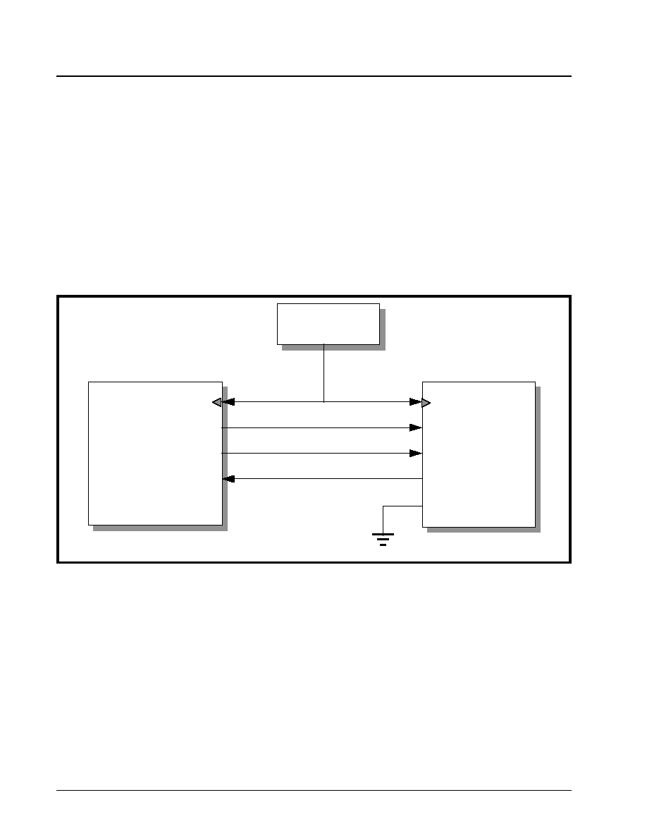
XRT7250
DS3/E3 FRAMER IC
·Á
·Á
·Á
·Á
REV. 1.1.1
138
The XRT7250 will receive the DS3 payload data, in a
serial manner, via the TxSer input pin. The Transmit
Payload Data Input Interface (within the XRT7250)
will latch this data into its circuitry, on the rising edge
of the TxInClk input clock signal.
C. Delineation of outbound DS3 frames (Frame
Slave Mode)
The Transmit Section (of the XRT7250) will use the
TxInClk input as its timing reference, and will use the
TxFrameRef input signal as its framing reference. In
other words, the Transmit Section of the XRT7250 will
initiate frame generation upon the rising edge of the
TxFrameRef input signal).
D. Sampling of payload data, from the Terminal
Equipment
In Mode 2, the XRT7250 will sample the data, at the
TxSer input pin, on the rising edge of TxInClk.
Interfacing the Transmit Payload Data Input Inter-
face block (of the XRT7250) to the Terminal Equip-
ment for Mode 2 Operation
Figure 46 presents an illustration of the Transmit Pay-
load Data Input Interface block (within the XRT7250)
being interfaced to the Terminal Equipment, for Mode
2 operation.
Mode 2, Operation of the Terminal Equipment
As shown in Figure 46, both the Terminal Equipment
and the XRT7250 will be driven by an external
44.736MHz clock signal. The Terminal Equipment
will receive the 44.736MHz clock signal via its
DS3_Clock_In input pin, and the XRT7250 Framer IC
will receive the 44.736MHz clock signal via the TxIn-
Clk input pin.
The Terminal Equipment will serially output the pay-
load data of the outbound DS3 data stream, via the
DS3_Data_Out output pin, upon the rising edge of
the signal at the DS3_Clock_In input pin.
N
OTE
: The DS3_Data_Out output pin of the Terminal
Equipment is electrically connected to the TxSer input pin.
The XRT7250 Framer IC will latch the data, residing
on the TxSer input line, on the rising edge of the TxIn-
Clk signal.
In this case, the Terminal Equipment has the respon-
sibility of providing the framing reference signal by
pulsing its Tx_Start_of_Frame output signal (and in
turn, the TxFrameRef input pin of the XRT7250),
"High" for one-bit period, coincident with the first bit of
a new DS3 frame. Once the XRT7250 detects the
rising edge of the input at its TxFrameRef input pin, it
will begin generation of a new DS3 frame.
N
OTES
:
1. In this case, the Terminal Equipment is controlling
the start of Frame Generation, and is therefore
referred to as the Frame Master. Conversely, since
the XRT7250 does not control the generation of a
F
IGURE
46. I
LLUSTRATION
OF
THE
T
ERMINAL
E
QUIPMENT
BEING
INTERFACED
TO
THE
T
RANSMIT
P
AYLOAD
D
ATA
I
NPUT
I
NTERFACE
BLOCK
OF
THE
XRT7250
FOR
M
ODE
2 (S
ERIAL
/L
OCAL
-T
IMED
/F
RAME
-S
LAVE
) O
PERATION
Terminal Equipment
XRT7250 DS3 Framer
DS3_Data_Out
DS3_Clock_In
Tx_Start_of_Frame
DS3_Overhead_Ind
TxSer
TxInClk
TxFrameRef
TxOH_Ind
NibInt
44.736 MHz Clock
Source
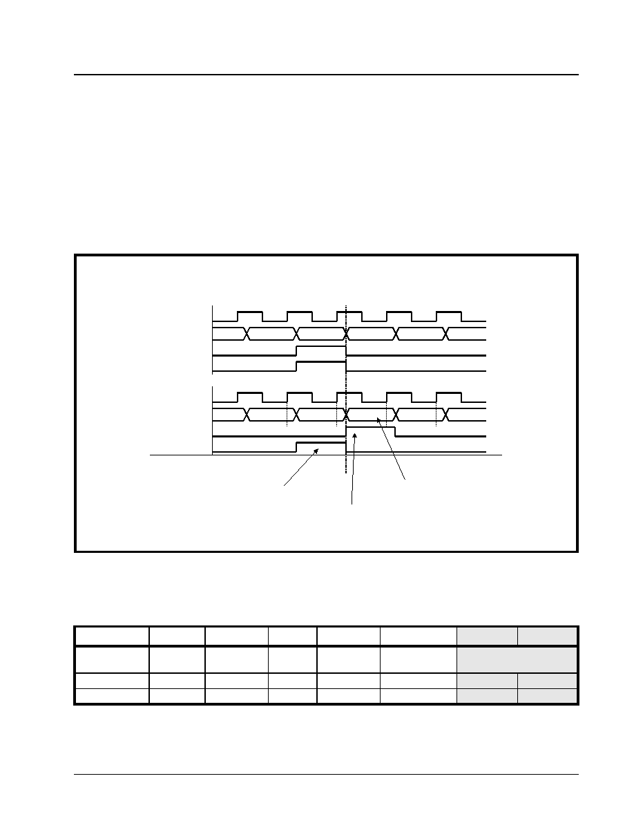
·Á
·Á
·Á
·Á
DS3/E3 FRAMER IC
XRT7250
REV. 1.1.1
139
new DS3 frame, but is rather driven by the Terminal
Equipment. Hence, the XRT7250 is referred to as
the Frame Slave.
2. If the user opts to configure the XRT7250 to oper-
ate in Mode 2, it is imperative that the
Tx_Start_of_Frame (or TxFrameRef) signal is syn-
chronized to the TxInClk input clock signal.
Finally, the XRT7250 will pulse its TxOH_Ind output
pin, one bit-period prior to it processing a given over-
head bit, within the outbound DS3 frame. Since the
TxOH_Ind output pin of the XRT7250 is electrically
connected to the DS3_Overhead_Ind, whenever the
XRT7250 pulses the TxOH_Ind output pin "High", it
will also be driving the DS3_Overhead_Ind input pin
(of the Terminal Equipment) "High". Whenever the
Terminal Equipment detects this pin toggling "High", it
should delay transmission of the very next DS3 frame
payload bit by one clock cycle.
The behavior of the signals between the XRT7250
and the Terminal Equipment for DS3 Mode 2 Opera-
tion is illustrated in Figure 47.
How to configure the XRT7250 to operate in this
mode.
1. Set the NibIntf input pin "Low".
2. Set the TimRefSel[1:0] bit-fields (within the
Framer Operating Mode Register) to "01" as
depicted below.
3. Interface the XRT7250, to the Terminal Equip-
ment, as illustrated in Figure 46.
4.2.1.3
Mode 3 - The Serial/Local-Timed/
Frame-Master Mode Behavior of the XRT7250
If the XRT7250 has been configured to operate in this
mode, then the XRT7250 will function as follows.
A. Local Timing - (Uses the TxInClk signal as the
Timing Reference)
F
IGURE
47. B
EHAVIOR
OF
THE
T
ERMINAL
I
NTERFACE
SIGNALS
BETWEEN
THE
XRT7250
AND
THE
T
ERMINAL
E
QUIP
-
MENT
(M
ODE
2 O
PERATION
)
Terminal Equipment Signals
DS3_Clock_In
DS3_Data_Out
Tx_Start_of_Frame
DS3_Overhead_Ind
XRT7250 Transmit Payload Data I/F Signals
TxInClk
TxSer
TxFrameRef
TxOH_Ind
Payload[4702]
Payload[4703]
X-Bit
Payload[1]
Payload[4702]
Payload[4703]
X-Bit
Payload[1]
Note: X-Bit will not be processed by the
Transmit Payload Data Input Interface.
DS3 Frame Number N
DS3 Frame Number N + 1
Note: TxFrame pulses high to denote
DS3 Frame Boundary.
Note: TxOH_Ind pulses high to
denote Overhead Data
(e.g., the X-bit).
FRAMER OPERATING MODE REGISTER (ADDRESS = 0X00)
B
IT
7
B
IT
6
B
IT
5
B
IT
4
B
IT
3
B
IT
2
B
IT
1
B
IT
0
Local Loopback
DS3/E3*
Internal LOS
Enable
RESET
Interrupt
Enable Reset
Frame Format
TimRefSel[1:0]
R/W
R/W
R/W
R/W
R/W
R/W
R/W
R/W
0
0
1
0
1
0
0
1
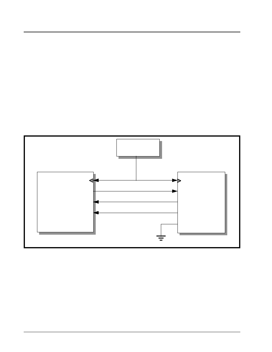
XRT7250
DS3/E3 FRAMER IC
·Á
·Á
·Á
·Á
REV. 1.1.1
140
In this mode, the Transmit Section of the XRT7250
will use the TxInClk signal as its timing reference.
B. Serial Mode
The XRT7250 will receive the DS3 payload data, in a
serial manner, via the TxSer input pin. The Transmit
Payload Data Input Interface (within the XRT7250)
will latch this data into its circuitry, on the rising edge
of the TxInClk input clock signal.
C. Delineation of outbound DS3 frames (Frame
Master Mode)
The Transmit Section of the XRT7250 will use the Tx-
InClk signal as its timing reference, and will initiate
DS3 frame generation, asynchronously with respect
to any externally applied signal. The XRT7250 will
pulse its TxFrame output pin "High" whenever its it
processing the very last bit-field within a given DS3
frame.
D. Sampling of payload data, from the Terminal
Equipment
In Mode 3, the XRT7250 will sample the data, at the
TxSer input pin, on the rising edge of TxInClk.
Interfacing the Transmit Payload Data Input Inter-
face block of the XRT7250 to the Terminal Equip-
ment for Mode 3 Operation
Figure 48 presents an illustration of the Transmit Pay-
load Data Input Interface block (within the XRT7250)
being interfaced to the Terminal Equipment, for Mode
3 operation.
Mode 3 Operation of the Terminal Equipment
In Figure 48, both the Terminal Equipment and the
XRT7250 are driven by an external 44.736MHz clock
signal. This clock signal is connected to the
DS3_Clock_In input of the Terminal Equipment and
the TxInClk input pin of the XRT7250.
The Terminal Equipment will serially output the pay-
load data on its DS3_Data_Out output pin, upon the
rising edge of the signal at the DS3_Clock_In input
pin. Similarly, the XRT7250 will latch the data, resid-
ing on the TxSer input pin, on the rising edge of TxIn-
Clk.
The XRT7250 will pulse the TxFrame output pin
"High" for one bit-period, coincident while it is pro-
cessing the last bit-field within a given outbound DS3
frame. The Terminal Equipment is expected to moni-
tor the TxFrame signal (from the XRT7250) and to
place the first bit, within the very next outbound DS3
frame on the TxSer input pin.
N
OTE
: In this case, the XRT7250 dictates exactly when the
very next DS3 frame will be generated.
The Terminal Equipment is expected to respond ap-
propriately by providing the XRT7250 with the first bit
of the new DS3 frame, upon demand. Hence, in this
mode, the XRT7250 is referred to as the Frame Mas-
F
IGURE
48. I
LLUSTRATION
OF
THE
T
ERMINAL
E
QUIPMENT
BEING
INTERFACED
TO
THE
T
RANSMIT
P
AYLOAD
D
ATA
I
NPUT
I
NTERFACE
BLOCK
OF
THE
XRT7250
FOR
M
ODE
3 (S
ERIAL
/L
OCAL
-T
IMED
/F
RAME
-M
ASTER
) O
PERATION
Terminal Equipment
XRT7250 DS3 Framer
DS3_Data_Out
DS3_Clock_In
Tx_Start_of_Frame
DS3_Overhead_Ind
TxSer
TxInClk
TxFrame
TxOH_Ind
NibInt
44.736 MHz Clock
Source
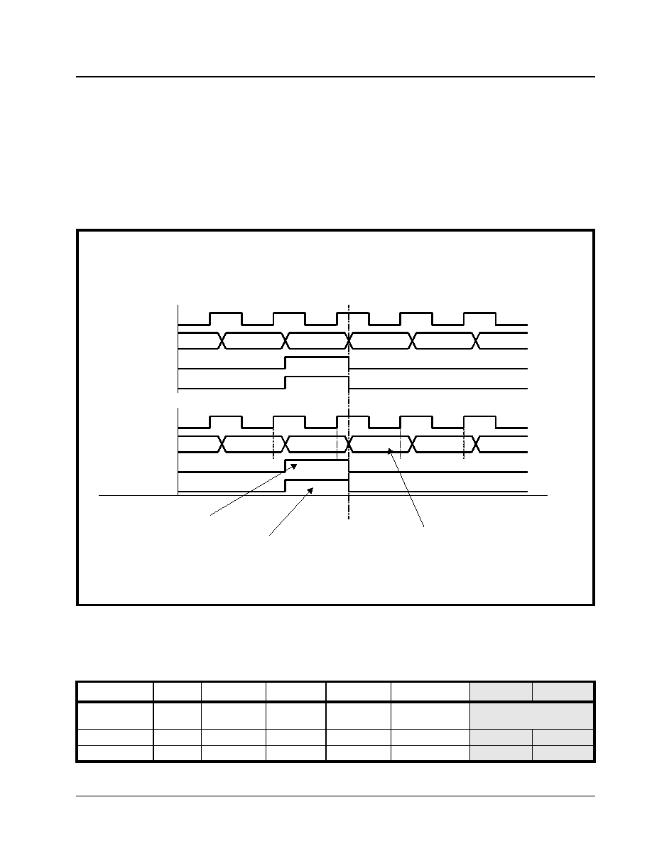
·Á
·Á
·Á
·Á
DS3/E3 FRAMER IC
XRT7250
REV. 1.1.1
141
ter and the Terminal Equipment is referred to as the
Frame Slave.
Finally, the XRT7250 will pulse its TxOH_Ind output
pin, one bit-period prior to it processing a given over-
head bit, within the outbound DS3 frame. Since the
TxOH_Ind output pin (of the XRT7250) is electrically
connected to the DS3_Overhead_Ind whenever the
XRT7250 pulses the TxOH_Ind output pin "High", it
will also be driving the DS3_Overhead_Ind input pin
(of the Terminal Equipment) "High". Whenever the
Terminal Equipment detects this pin toggling "High", it
should delay transmission of the very next DS3 frame
payload bit by one clock cycle.
The behavior of the signal between the XRT7250 and
the Terminal Equipment for DS3 Mode 3 Operation is
illustrated in Figure 49.
How to configure the XRT7250 to operate in this
mode.
1. Set the NibIntf input pin "Low".
2. Set the TimRefSel[1:0] bit-fields (within the
Framer Operating Mode Register) to "10" or "11"
as depicted below.
3. Interface the XRT7250, to the Terminal Equip-
ment, as illustrated in Figure 48.
F
IGURE
49. B
EHAVIOR
OF
THE
T
ERMINAL
I
NTERFACE
SIGNALS
BETWEEN
THE
XRT7250
AND
THE
T
ERMINAL
E
QUIP
-
MENT
(DS3 M
ODE
3 O
PERATION
)
Terminal Equipment Signals
DS3_Clock_In
DS3_Data_Out
Tx_Start_of_Frame
DS3_Overhead_Ind
XRT7250 Transmit Payload Data I/F Signals
TxInClk
TxSer
TxFrame
TxOH_Ind
Payload[4702]
Payload[4703]
X-Bit
Payload[1]
Payload[4702]
Payload[4703]
X-Bit
Payload[1]
Note: X-Bit will not be processed by the
Transmit Payload Data Input Interface.
DS3 Frame Number N
DS3 Frame Number N + 1
Note: TxFrame pulses high to denote
DS3 Frame Boundary.
Note: TxOH_Ind pulses high to
denote Overhead Data
(e.g., the X-bit).
FRAMER OPERATING MODE REGISTER (ADDRESS = 0X00)
B
IT
7
B
IT
6
B
IT
5
B
IT
4
B
IT
3
B
IT
2
B
IT
1
B
IT
0
Local Loopback
DS3/E3*
Internal LOS
Enable
RESET
Interrupt
Enable Reset
Frame Format
TimRefSel[1:0]
R/W
R/W
R/W
R/W
R/W
R/W
R/W
R/W
0
0
1
0
1
0
1
X
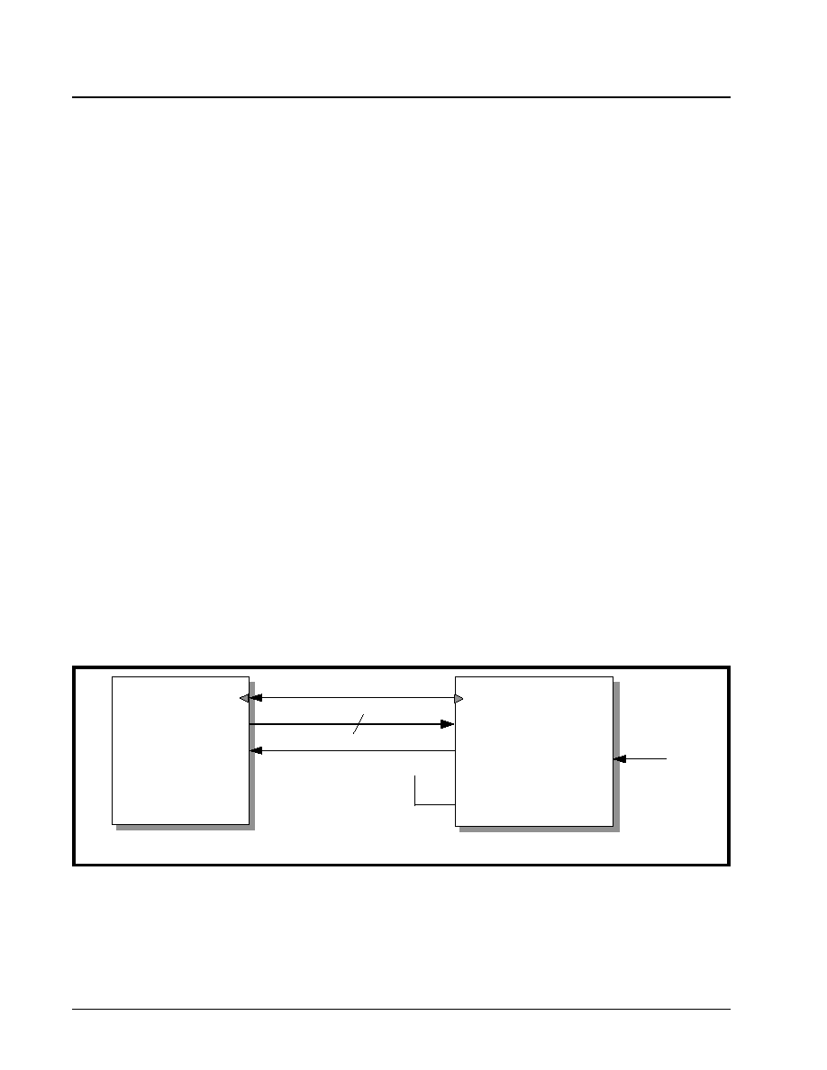
XRT7250
DS3/E3 FRAMER IC
·Á
·Á
·Á
·Á
REV. 1.1.1
142
4.2.1.4
Mode 4 - The Nibble-Parallel/Loop-
Timed Mode Behavior of the XRT7250
If the XRT7250 has been configured to operate in this
mode, then the XRT7250 will behave as follows.
A. Looped Timing (Uses the RxLineClk as the
Timing Reference)
In this mode, the Transmit Section of the XRT7250
will use the RxLineClk signal as its timing reference.
When the XRT7250 is operating in the Nibble-Mode,
it will internally divide the RxLineClk signal, by a fac-
tor of four (4) and will output this signal via the TxNib-
Clk output pin.
B. Nibble-Parallel Mode
The XRT7250 will accept the DS3 payload data, from
the Terminal Equipment in a nibble-parallel manner,
via the TxNib[3:0] input pins. The Transmit Terminal
Equipment Input Interface block will latch this data in-
to its circuitry, on the rising edge of the TxNibClk out-
put signal.
C. Delineation of the outbound DS3 frames
The XRT7250 will pulse the TxNibFrame output pin
"High" for one bit-period coincident with the XRT7250
processing the last nibble of a given DS3 frame.
D. Sampling of payload data, from the Terminal
Equipment
In Mode 4, the XRT7250 will sample the data, at the
TxNib[3:0] input pins, on the third rising edge of the
RxOutClk clock signal, following a pulse in the TxNib-
Clk signal (see Figure 51).
N
OTE
: The TxNibClk signal, from the XRT7250 operates
nominally at 11.184 MHz (e.g., 44.736 MHz divided by 4).
However, for reasons described below, TxNibClk effectively
operates at a "Low"er clock frequency. The Transmit Pay-
load Data Input Interface is only used to accept the payload
data, which is intended to be carried by outbound DS3
frames. The Transmit Payload Data Input Interface is not
designed to accommodate the entire DS3 data stream.
The DS3 Frame consists of 4704 payload bits or 1176
nibbles. Therefore, the XRT7250 will supply 1176 Tx-
NibClk pulses between the rising edges of two con-
secutive TxNibFrame pulses. The DS3 Frame repeti-
tion rate is 9.398kHz. Hence, 1176 TxNibClk pulses
for each DS3 frame period amounts to TxNibClk run-
ning at approximately 11.052 MHz. The method by
which the 1176 TxNibClk pulses are distributed
throughout the DS3 frame period is presented below.
Nominally, the Transmit Section within the XRT7250
will generate a TxNibClk pulse for every 4 RxOutClk
(or TxInClk) periods. However, in 14 cases (within a
DS3 frame period), the Transmit Payload Data Input
Interface will allow 5 TxInClk periods to occur be-
tween two consecutive TxNibClk pulses.
Interfacing the Transmit Payload Data Input Inter-
face block of the XRT7250 to the Terminal Equip-
ment for Mode 4 Operation
Figure 50 presents an illustration of the Transmit Pay-
load Data Input Interface block (within the XRT7250)
being interfaced to the Terminal Equipment, for Mode
4 Operation.
Mode 4 Operation of the Terminal Equipment
When the XRT7250 is operating in this mode, it will
function as the source of the 11.184MHz (e.g., the
44.736MHz clock signal divided by "4") clock signal,
that will be used as the Terminal Equipment Interface
clock by both the XRT7250 and the Terminal Equip-
ment.
The Terminal Equipment will output the payload data
of the outbound DS3 data stream via its
DS3_Data_Out[3:0] pins on the rising edge of the
11.184MHz clock signal at the DS3_Nib_Clock_In in-
put pin.
The XRT7250 will latch the outbound DS3 data
stream (from the Terminal Equipment) on the rising
F
IGURE
50. I
LLUSTRATION
OF
THE
T
ERMINAL
E
QUIPMENT
BEING
INTERFACED
TO
THE
T
RANSMIT
P
AYLOAD
D
ATA
I
NPUT
I
NTERFACE
BLOCK
OF
THE
XRT7250
FOR
M
ODE
4 (N
IBBLE
-P
ARALLEL
/L
OOP
-T
IMED
) O
PERATION
Terminal Equipment
XRT7250 DS3 Framer
DS3_Data_Out[3:0]
DS3_Nib_Clock_In
Tx_Start_of_Frame
TxNib[3:0]
TxNibClk
TxNibFrame
NibInt
VCC
4
RxLineClk
44.736MHz
11.184MHz

·Á
·Á
·Á
·Á
DS3/E3 FRAMER IC
XRT7250
REV. 1.1.1
143
edge of the TxNibClk output clock signal. The
XRT7250 will indicate that it is processing the last
nibble, within a given DS3 frame, by pulsing its TxNib-
Frame output pin "High" for one TxNibClk clock peri-
od. When the Terminal Equipment detects a pulse at
its Tx_Start_of_Frame input pin, it is expected to
transmit the first nibble, of the very next outbound
DS3 frame to the XRT7250 via the
DS3_Data_Out[3:0] (or TxNib[3:0] pins).
Finally, for the Nibble-Parallel Mode operation, the
XRT7250 will continuously pull the TxOHInd output
pin "Low".
The behavior of the signals between the XRT7250
and the Terminal Equipment for DS3 Mode 4 Opera-
tion is illustrated in Figure 51.
How to configure the XRT7250 into Mode 4
1. Set the NibIntf input pin "High".
2. Set the TimRefSel[1:0] bit-fields (within the
Framer Operating Mode Register) to "00" as illus-
trated below.
F
IGURE
51. B
EHAVIOR
OF
THE
T
ERMINAL
I
NTERFACE
SIGNALS
BETWEEN
THE
XRT7250
AND
THE
T
ERMINAL
E
QUIP
-
MENT
(M
ODE
4 O
PERATION
)
Terminal Equipment Signals
XRT7250 Transmit Payload Data I/F Signals
DS3 Frame Number N
DS3 Frame Number N + 1
Note: TxNibFrame pulses high to denote
DS3 Frame Boundary.
RxOutClk
Tx_Start_of_Frame
DS3_Nib_Clock_In
DS3_Data_Out[3:0]
Nibble [1175]
Nibble [0]
RxOutClk
TxNibFrame
TxNibClk
TxNib[3:0]
Nibble [1175]
Nibble [0]
Sampling Edge of XRT7250 Device
FRAMER OPERATING MODE REGISTER (ADDRESS = 0X00)
B
IT
7
B
IT
6
B
IT
5
B
IT
4
B
IT
3
B
IT
2
B
IT
1
B
IT
0
Local Loopback
DS3/E3*
Internal LOS
Enable
RESET
Interrupt
Enable Reset
Frame Format
TimRefSel[1:0]
R/W
R/W
R/W
R/W
R/W
R/W
R/W
R/W
0
0
1
0
1
0
0
0

XRT7250
DS3/E3 FRAMER IC
·Á
·Á
·Á
·Á
REV. 1.1.1
144
3. Interface the XRT7250, to the Terminal Equip-
ment, as illustrated in Figure 50.
N
OTE
: The XRT7250 Framer IC cannot support the Framer
Local Loop-back Mode of operation. The user must config-
ure the XRT7250 Framer IC into any of the following modes,
prior to configuring the Framer Local-Loop-back Mode
operation.
∑ Mode 2 - Serial/Local-Timed/Frame-Slave Mode.
∑ Mode 3 - Serial/Local-Timed/Frame-Master Mode.
∑ Mode 5 - Nibble-Parallel/Local-Timed/Frame-Slave
Mode.
∑ Mode 6 - Nibble-Parallel/Local-Timed/Frame-Mas-
ter Mode.
For more detailed information on the Framer Local
Loop-back Mode Operation, please see Section 6.0.
4.2.1.5
Mode 5 - The Nibble-Parallel/Local-
Timed/Frame-Slave Interface Mode Behavior of
the XRT7250
If the XRT7250 has been configured to operate in this
mode, then the XRT7250 will function as follows:
A. Local-Timed (Uses the TxInClk signal as the
Timing Reference)
In this mode, the Transmit Section of the XRT7250
will use the TxInClk signal at its timing reference.
Further, the chip will internally divide the TxInClk
clock signal by a factor of 4 and will output this divid-
ed clock signal via the TxNibClk output pin. The
Transmit Terminal Equipment Input Interface block
(within the XRT7250) will use the rising edge of the
TxNibClk signal, to latch the data, residing on the Tx-
Nib[3:0] into its circuitry.
B. Nibble-Parallel Mode
The XRT7250 will accept the DS3 payload data, from
the Terminal Equipment, in a parallel manner, via the
TxNib[3:0] input pins. The Transmit Terminal Equip-
ment Input Interface will latch this data into its circuit-
ry, on the rising edge of the TxNibClk output signal.
C. Delineation of outbound DS3 Frames
The Transmit Section will use the TxInClk input signal
as its timing reference and will use the TxFrameRef
input signal as its Framing Reference (e.g., the Trans-
mit Section of the XRT7250 initiates frame generation
upon the rising edge of the TxFrameRef signal).
N
OTE
: In this case, the Terminal Equipment should pulse
the TxFrameRef input signal (of the XRT7250 Framer IC)
coincident with it applying the first payload nibble, within a
given outbound DS3 frame. Hence, the duration of this
pulse should be one nibble-period of the DS3 signal (see
Figure 53).
D. Sampling of payload data, from the Terminal
Equipment
In Mode 5, the XRT7250 will sample the data, at the
TxNib[3:0] input pins, on the third rising edge of the
TxInClk clock signal, following a pulse in the TxNibClk
signal (see Figure 53).
N
OTE
: The TxNibClk signal, from the XRT7250 operates
nominally at 11.184 MHz (e.g., 44.736 MHz divided by 4).
However, for reasons described below, TxNibClk effectively
operates at a "Low"er clock frequency. The Transmit Pay-
load Data Input Interface is only used to accept the payload
data, which is intended to be carried by outbound DS3
frames. The Transmit Payload Data Input Interface is not
designed to accommodate the entire DS3 data stream.
The DS3 Frame consists of 4704 payload bits or 1176
nibbles. Therefore, the XRT7250 will supply 1176 Tx-
NibClk pulses between the rising edges of two con-
secutive TxNibFrame pulses. The DS3 Frame repeti-
tion rate is 9.398kHz. Hence, 1176 TxNibClk pulses
for each DS3 frame period amounts to TxNibClk run-
ning at approximately 11.052 MHz. The method by
which the 1176 TxNibClk pulses are distributed
throughout the DS3 frame period is presented below.
Nominally, the Transmit Section within the XRT7250
will generate a TxNibClk pulse for every 4 RxOutClk
(or TxInClk) periods. However, in 14 cases (within a
DS3 frame period), the Transmit Payload Data Input
Interface will allow 5 TxInClk periods to occur be-
tween two consecutive TxNibClk pulses.
Interfacing the Transmit Payload Data Input Inter-
face block of the XRT7250 to the Terminal Equip-
ment for Mode 5 Operation
Figure 52 presents an illustration of the Transmit Pay-
load Data Input Interface block (within the XRT7250)
being interfaced to the Terminal Equipment, for Mode
5 Operation.
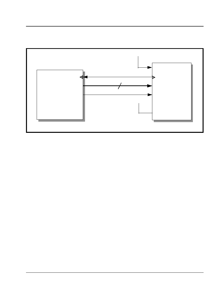
·Á
·Á
·Á
·Á
DS3/E3 FRAMER IC
XRT7250
REV. 1.1.1
145
Mode 5 Operation of the Terminal Equipment
In Figure 52 both the Terminal Equipment and the
XRT7250 will be driven by an external 11.184MHz
clock signal. The Terminal Equipment will receive the
11.184MHz clock signal via the DS3_Nib_Clock_In
input pin. The XRT7250 will output the 11.184MHz
clock signal via the TxNibClk output pin.
The Terminal Equipment will serially output the data
on the DS3_Data_Out[3:0] pins, upon the rising edge
of the signal at the DS3_Clock_In input pin.
N
OTE
: The DS3_Data_Out[3:0] output pins of the Terminal
Equipment is electrically connected to the TxNib[3:0] input
pins.
The XRT7250 will latch the data, residing on the Tx-
Nib[3:0] input pins, on the rising edge of the TxNibClk
signal.
In this case, the Terminal Equipment has the respon-
sibility of providing the framing reference signal by
pulsing the Tx_Start_of_Frame output pin (and in
turn, the TxFrameRef input pin of the XRT7250)
"High" for one bit-period, coincident with the first nib-
ble of a new DS3 frame. Once the XRT7250 detects
the rising edge of the input at its TxFrameRef input
pin, it will begin generation of a new DS3 frame.
Finally, the XRT7250 will always internally generate
the Overhead bits, when it is operating in both the
DS3 and Nibble-parallel modes. The XRT7250 will
pull the TxOHInd input pin "Low".
The behavior of the signals between the XRT7250
and the Terminal Equipment for DS3 Mode 5 Opera-
tion is illustrated in Figure 53.
F
IGURE
52. I
LLUSTRATION
OF
THE
T
ERMINAL
E
QUIPMENT
BEING
INTERFACED
TO
THE
T
RANSMIT
P
AYLOAD
D
ATA
I
NPUT
I
NTERFACE
BLOCK
OF
THE
XRT7250
FOR
M
ODE
5 (N
IBBLE
-P
ARALLEL
/L
OCAL
-T
IMED
/F
RAME
-S
LAVE
) O
PERA
-
TION
Terminal Equipment
XRT7250 DS3 Framer
DS3_Data_Out[3:0]
DS3_Nib_Clock_In
Tx_Start_of_Frame
TxNib[3:0]
TxNibClk
TxFrameRef
NibInt
VCC
4
44.736MHz Clock Source
TxInClk
11.184MHz
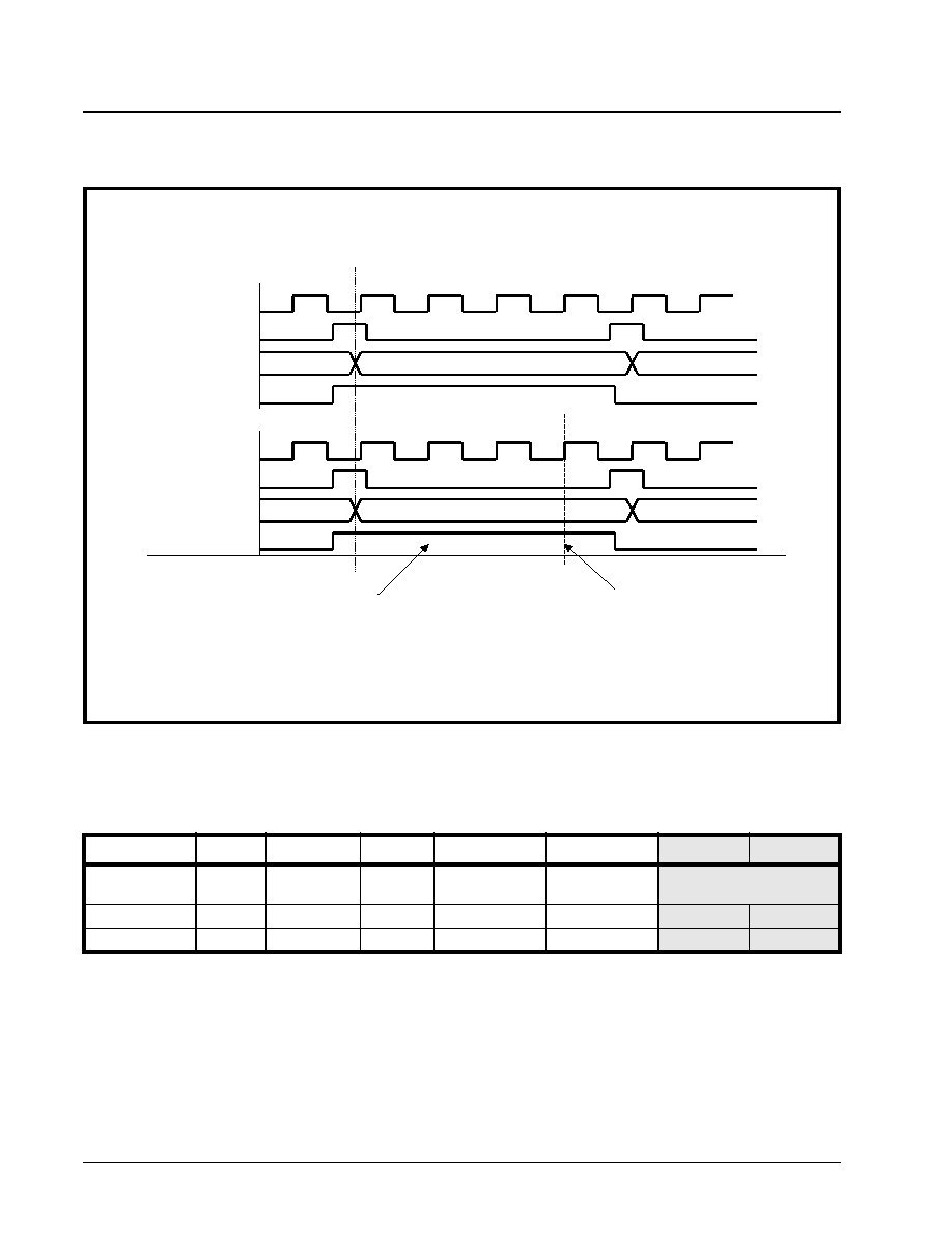
XRT7250
DS3/E3 FRAMER IC
·Á
·Á
·Á
·Á
REV. 1.1.1
146
How to configure the XRT7250 into Mode 5
1. Set the NibIntf input pin "High".
2. Set the TimRefSel[1:0] bit-fields (within the
Framer Operating Mode Register) to "01" as illus-
trated below.
3. Interface the XRT7250, to the Terminal Equip-
ment, as illustrated in Figure 52.
4.2.1.6
Mode 6 - The Nibble-Parallel/TxInClk/
Frame-Master Interface Mode Behavior of the
XRT7250
If the XRT7250 has been configured to operate in this
mode, then the XRT7250 will function as follows:
A. Local-Timed (Uses the TxInClk signal as the
Timing Reference)
In this mode, the Transmit Section of the XRT7250
will use the TxInClk signal at its timing reference.
Further, the chip will internally divide the TxInClk
clock signal by a factor of 4 and will output this divid-
ed clock signal via the TxNibClk output pin. The
Transmit Terminal Equipment Input Interface block
(within the XRT7250) will use the rising edge of the
TxNibClk signal, to latch the data, residing on the Tx-
Nib[3:0] into its circuitry.
F
IGURE
53. B
EHAVIOR
OF
THE
T
ERMINAL
I
NTERFACE
SIGNALS
BETWEEN
THE
XRT7250
AND
THE
T
ERMINAL
E
QUIP
-
MENT
(DS3 M
ODE
5 O
PERATION
)
Terminal Equipment Signals
XRT7250 Transmit Payload Data I/F Signals
DS3 Frame Number N
DS3 Frame Number N + 1
Note: TxFrameRef is pulsed high to denote
first nibble within a new DS3 frame
TxInClk
Tx_Start_of_Frame
DS3_Nib_Clock_In
DS3_Data_Out[3:0]
Nibble [0]
Nibble [1]
TxInClk
TxFrameRef
TxNibClk
TxNib[3:0]
Nibble [0]
Nibble [1]
Nibble [1175]
Nibble [1175]
Sampling edge of the XRT7250
Device
FRAMER OPERATING MODE REGISTER (ADDRESS = 0X00)
B
IT
7
B
IT
6
B
IT
5
B
IT
4
B
IT
3
B
IT
2
B
IT
1
B
IT
0
Local Loopback
DS3/E3*
Internal LOS
Enable
RESET
Interrupt
Enable Reset
Frame Format
TimRefSel[1:0]
R/W
R/W
R/W
R/W
R/W
R/W
R/W
R/W
0
0
1
0
1
0
0
1
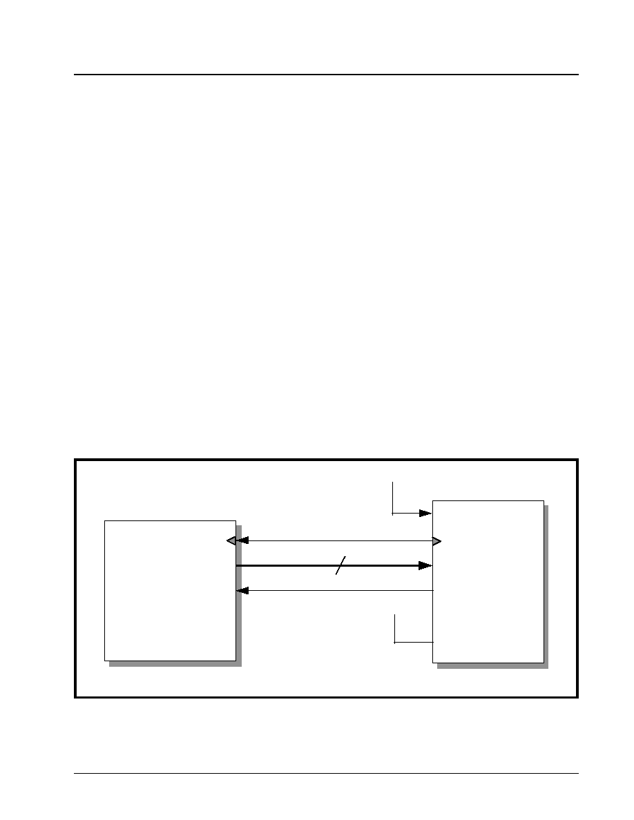
·Á
·Á
·Á
·Á
DS3/E3 FRAMER IC
XRT7250
REV. 1.1.1
147
B. Nibble-Parallel Mode
The XRT7250 will accept the DS3 payload data, from
the Terminal Equipment, in a parallel manner, via the
TxNib[3:0] input pins. The Transmit Terminal Equip-
ment Input Interface will latch this data into its circuit-
ry, on the rising edge of the TxNibClk output signal.
C. Delineation of outbound DS3 Frames
The Transmit Section will use the TxInClk input signal
as its timing reference and will initiate the generation
of DS3 frames, asynchronous with respect to any ex-
ternal signal. The XRT7250 will pulse the TxFrame
output pin "High" whenever it is processing the last
nibble, within a given outbound DS3 frame.
D. Sampling of payload data, from the Terminal
Equipment
In Mode 6, the XRT7250 will sample the data, at the
TxNib[3:0] input pins, on the third rising edge of the
TxInClk clock signal, following a pulse in the TxNibClk
signal (see Figure 55).
N
OTE
: The TxNibClk signal from the XRT7250, operates
nominally at 11.184 MHz (e.g., 44.736 MHz divided by 4).
However, for reasons described below, TxNibClk effectively
operates at a "Low"er clock frequency. The Transmit Pay-
load Data Input Interface is only used to accept the payload
data, which is intended to be carried by outbound DS3
frames. The Transmit Payload Data Input Interface is not
designed to accommodate the entire DS3 data stream.
The DS3 Frame consists of 4704 payload bits or 1176
nibbles. Therefore, the XRT7250 will supply 1176 Tx-
NibClk pulses between the rising edges of two con-
secutive TxNibFrame pulses. The DS3 Frame repeti-
tion rate is 9.398kHz. Hence, 1176 TxNibClk pulses
for each DS3 frame period amounts to TxNibClk run-
ning at approximately 11.052 MHz. The method by
which the 1176 TxNibClk pulses are distributed
throughout the DS3 frame period is presented below.
Nominally, the Transmit Section within the XRT7250
will generate a TxNibClk pulse for every 4 RxOutClk
(or TxInClk) periods. However, in 14 cases (within a
DS3 frame period), the Transmit Payload Data Input
Interface will allow 5 TxInClk periods to occur be-
tween two consecutive TxNibClk pulses.
Interfacing the Transmit Payload Data Input Inter-
face block of the XRT7250 to the Terminal Equip-
ment for Mode 6 Operation
Figure 54 presents an illustration of the Transmit Pay-
load Data Input Interface block (within the XRT7250)
being interfaced to the Terminal Equipment, for Mode
6 Operation.
Mode 6, Operation of the Terminal Equipment
In Figure 54 both the Terminal Equipment and the
XRT7250 will be driven by an external 11.184MHz
clock signal. The Teriminal Equipment will receive
the 11.184MHz clock signal via the
DS3_Nib_Clock_In input pin. The XRT7250 will out-
put the 11.184MHz clock signal via the TxNibClk out-
put pin.
F
IGURE
54. I
LLUSTRATION
OF
THE
T
ERMINAL
E
QUIPMENT
BEING
INTERFACED
TO
THE
T
RANSMIT
P
AYLOAD
D
ATA
I
NPUT
I
NTERFACE
BLOCK
OF
THE
XRT7250
FOR
M
ODE
6 (N
IBBLE
-P
ARALLEL
/L
OCAL
-T
IMED
/F
RAME
-M
ASTER
)
O
PERATION
Terminal Equipment
XRT7250 DS3 Framer
DS3_Data_Out[3:0]
DS3_Nib_Clock_In
Tx_Start_of_Frame
TxNib[3:0]
TxNibClk
TxNibFrame
NibInt
VCC
4
44.736MHz Clock Source
TxInClk
11.184MHz
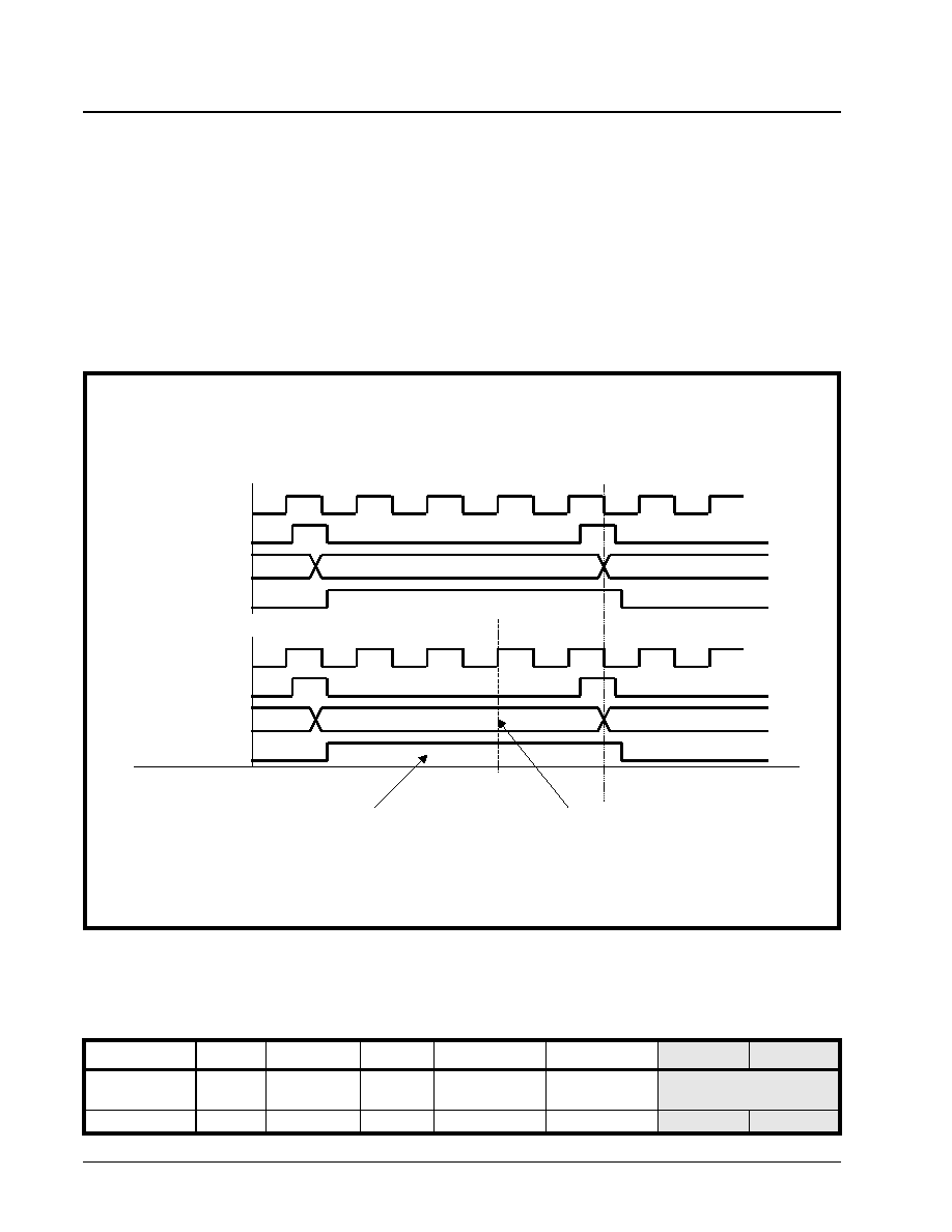
XRT7250
DS3/E3 FRAMER IC
·Á
·Á
·Á
·Á
REV. 1.1.1
148
The Terminal Equipment will serially output the data
on the DS3_Data_Out[3:0] pins upon the rising edge
of the signal at the DS3_Clock_In input pin. The
XRT7250 will latch the data, residing on the Tx-
Nib[3:0] input pins, on the rising edge of the TxNibClk
signal.
In this case the XRT7250 has the responsibility of
providing the framing reference signal by pulsing the
TxFrame output pin (and in turn the
Tx_Start_of_Frame input pin of the Terminal Equip-
ment) "High" for one bit-period, coincident with the
last bit within a given DS3 frame.
Finally, the XRT7250 will always internally generate
the Overhead bits, when it is operating in both the
DS3 and Nibble-parallel modes. The XRT7250 will
pull the TxOHInd input pin "Low".
The behavior of the signals between the XRT7250
and the Terminal Equipment for DS3 Mode 6 Opera-
tion is illustrated in Figure 55.
How to configure the XRT7250 into Mode 6
1. Set the NibInt input pin "High".
2. Set the TimRefSel[1:0] bit-fields (within the
Framer Operating Mode Register) to 1X as illus-
trated below.
F
IGURE
55. B
EHAVIOR
OF
THE
T
ERMINAL
I
NTERFACE
SIGNALS
BETWEEN
THE
XRT7250
AND
THE
T
ERMINAL
E
QUIP
-
MENT
(DS3 M
ODE
6 O
PERATION
)
Terminal Equipment Signals
XRT7250 Transmit Payload Data I/F Signals
DS3 Frame Number N
DS3 Frame Number N + 1
Note: TxNibFrame pulses high to denote
DS3 Frame Boundary.
TxInClk
Tx_Start_of_Frame
DS3_Nib_Clock_In
DS3_Data_Out[3:0]
Nibble [1175]
Nibble [0]
TxInClk
TxNibFrame
TxNibClk
TxNib[3:0]
Nibble [1175]
Nibble [0]
Sampling Edge of the XRT7250 Device
FRAMER OPERATING MODE REGISTER (ADDRESS = 0X00)
B
IT
7
B
IT
6
B
IT
5
B
IT
4
B
IT
3
B
IT
2
B
IT
1
B
IT
0
Local Loopback
DS3/E3*
Internal LOS
Enable
RESET
Interrupt
Enable Reset
Frame Format
TimRefSel[1:0]
R/W
R/W
R/W
R/W
R/W
R/W
R/W
R/W

·Á
·Á
·Á
·Á
DS3/E3 FRAMER IC
XRT7250
REV. 1.1.1
149
3. Interface the XRT7250, to the Terminal Equip-
ment, as illustrated in Figure 54.
4.2.2
The Transmit Overhead Data Input Inter-
face
Figure 56 presents a simple illustration of the Trans-
mit Overhead Data Input Interface block within the
XRT7250.
The DS3 Frame consists of 4760 bits. Of these bits,
4704 bits are payload bits and the remaining 56 bits
are overhead bits. The XRT7250 has been designed
to handle and process both the payload type and
overhead type bits for each DS3 frame. Within the
Transmit Section within the XRT7250, the Transmit
Payload Data Input Interface has been designed to
handle the payload data. Likewise, the Transmit
Overhead Data Input Interface has been designed to
handle and process the overhead bits.
The Transmit Section of the XRT7250 generates or
processes the various overhead bits within the DS3
frame, in the following manner.
The Frame Synchronization Overhead Bits (e.g.,
the F and M bits)
The F and M bits are always internally generated by
the Transmit Section of the XRT7250. These over-
head bits are used (by the Remote Terminal Equip-
ment) for Frame Synchronization purposes. Hence,
the user cannot insert his/her value for the F and M
bits into the outbound DS3 data stream, via the
Transmit Overhead Data Input Interface. Any attempt
to externally insert values for the "F" and "M" bits, will
be ignored by the Transmit Overhead Data Input In-
terface"High" block.
The Performance Monitoring Overhead Bits (P
and CP Bits)
The P-bits are always internally generated by the
Transmit Section of the XRT7250. The "P" bits are
used by the Remote Terminal Equipment to perform
0
0
1
0
1
0
1
x
FRAMER OPERATING MODE REGISTER (ADDRESS = 0X00)
B
IT
7
B
IT
6
B
IT
5
B
IT
4
B
IT
3
B
IT
2
B
IT
1
B
IT
0
F
IGURE
56. S
IMPLE
I
LLUSTRATION
OF
THE
T
RANSMIT
O
VERHEAD
D
ATA
I
NPUT
I
NTERFACE
BLOCK
Transmit
Overhead
Data Input
Interface Block
Transmit
Overhead
Data Input
Interface Block
TxOHFrame
TxOHEnable
TxOH
TxOHClk
TxOHIns
To Transmit DS3 Framer Block

XRT7250
DS3/E3 FRAMER IC
·Á
·Á
·Á
·Á
REV. 1.1.1
150
error-checking/detection of a DS3 data stream, as it
is transmitted from one Terminal Equipment to adja-
cent Terminal Equipment (e.g., point-to-point check-
ing). Hence, the user cannot insert his/her value for
the P-bits into the outbound DS3 data stream, via the
Transmit Overhead Data Input Interface.
In contrast to "P" bits, "CP" bits are used perform er-
ror-checking/detection of a DS3 data stream from the
Source Terminal Equipment to the Sink Terminal
Equipment. In applications where a given DS3 data
stream is received via one port, and is output via an-
other port, it is necessary that the "CP" bit-values re-
main constant. The only way to insure this to (1) ex-
tract out the "CP" bit values, via the Receiving Line
Card and (2) insert these CP-bit values into the out-
bound DS3 data stream, via the Transmit Overhead
Data Input Interface block. Hence, the Transmit Over-
head Data Input Interface block will permit the user to
externally insert the "CP" bits into the outbound DS3
data stream.
The Alarm and signaling related Overhead bits
Bits that are used to transport the alarm conditions
can be either internally generated by the Transmit
Section within the XRT7250, or can be externally
generated and inserted into the outbound DS3 data
stream, via the Transmit Overhead Data Input Inter-
face. The DS3 frame overhead bits that fall into this
category are:
∑ The X bits
∑ The FEAC bits
∑ The FEBE bits.
The Data Link Related Overhead Bits
The DS3 frame structure also contains bits which can
be used to transport User Data Link information and
Path Maintenance Data Link information. The UDL
(User Data Link) bits are only accessible via the
Transmit Overhead Data Input Interface. The Path
Maintenance Data Link (PMDL) bits can either be
sourced from the Transmit LAPD Controller/Buffer or
via the Transmit Overhead Data Input Interface.
Table 19 lists the Overhead Bits within the DS3 frame.
Additionally, this table also indicates whether or not
these overhead bits can be sourced by the Transmit
Overhead Data Input Interface or not.
N
OTES
:
* The XRT7250 contains mask register bits that per-
mit the user to alter the state of the internally generat-
ed value for these bits.
+ The Transmit LAPD Controller/Buffer can be config-
ured to be the source of the DL bits, within the out-
bound DS3 data stream.
In all, the Transmit Overhead Data Input Interface
permits the user to insert overhead data into the out-
bound DS3 frames via the following two different
methods.
∑ Method 1 - Using the TxOHClk clock signal
∑ Method 2 - Using the TxInClk and the TxOHEnable
signals.
Each of these methods are described below.
4.2.2.1
4.2.2.1 Method 1 - Using the TxOHClk
Clock Signal
The Transmit Overhead Data Input Interface consists
of the five signals. Of these five (5) signals, the fol-
lowing four (4) signals are to be used when imple-
menting Method 1.
∑ TxOH
∑ TxOHClk
∑ TxOHFrame
T
ABLE
19: A L
ISTING
OF
THE
O
VERHEAD
BITS
WITHIN
THE
DS3
FRAME
,
AND
THEIR
POTENTIAL
SOURCES
,
WITHIN
THE
XRT7250 IC
O
VERHEAD
B
IT
I
NTERNALLY
GENERATED
A
CCESSIBLE
VIA
THE
T
RANSMIT
O
VERHEAD
D
ATA
I
NPUT
I
NTERFACE
B
UFFER
/R
EGISTER
A
CCESSIBLE
P
Yes
No
Yes*
X
Yes
Yes
Yes
F
Yes
No
Yes*
M
Yes
No
Yes*
FEAC
No
Yes
Yes
FEBE
Yes
Yes
Yes
DL
No
Yes
Yes+
UDL
No
Yes
No
CP
No
Yes
No

·Á
·Á
·Á
·Á
DS3/E3 FRAMER IC
XRT7250
REV. 1.1.1
151
∑ TxOHIns
Each of these signals are listed and described below.
Table 20.
Interfacing the Transmit Overhead Data Input In-
terface to the Terminal Equipment.
Figure 57 illustrates how one should interface the
Transmit Overhead Data Input Interface to the Termi-
nal Equipment, when using Method 1.
T
ABLE
20: D
ESCRIPTION
OF
M
ETHOD
1 T
RANSMIT
O
VERHEAD
I
NPUT
I
NTERFACE
S
IGNALS
N
AME
T
YPE
D
ESCRIPTION
TxOHIns
Input
Transmit Overhead Data Insert Enable input pin.
Asserting this input signal (e.g., setting it "High") enables the Transmit Overhead Data Input Inter-
face to accept overhead data from the Terminal Equipment. In other words, while this input pin is
"High", the Transmit Overhead Data Input Interface will sample the data at the TxOH input pin, on
the falling edge of the TxOHClk output signal.
Conversely, setting this pin "Low" configures the Transmit Overhead Data Input Interface to NOT
sample (e.g., ignore) the data at the TxOH input pin, on the falling edge of the TxOHClk output
signal.
N
OTE
: If the Terminal Equipment attempts to insert an overhead bit that cannot be accepted by
the Transmit Overhead Data Input Interface (e.g., if the Terminal Equipment asserts the TxOHIns
signal, at a time when one of these non-insertable overhead bits are being processed), that par-
ticular insertion effort will be ignored.
TxOH
Input
Transmit Overhead Data Input pin:
The Transmit Overhead Data Input Interface accepts the overhead data via this input
pin, and inserts into the overhead bit position within the very next outbound DS3 frame.
If the TxOHIns pin is pulled "High", the Transmit Overhead Data Input Interface will sam-
ple the data at this input pin (TxOH), on the falling edge of the TxOHClk output pin.
Conversely, if the TxOHIns pin is pulled "Low", then the Transmit Overhead Data Input
Interface will NOT sample the data at this input pin (TxOH). Consequently, this data will
be ignored.
TxOHClk
Output
Transmit Overhead Input Interface Clock Output signal:
This output signal serves two purposes:
1. The Transmit Overhead Data Input Interface will provide a rising clock edge on this signal, one
bit-period prior to the instant that the Transmit Overhead Data Input Interface is processing an
overhead bit.
2. The Transmit Overhead Data Input Interface will sample the data at the TxOH input, on the fall-
ing edge of this clock signal (provided that the TxOHIns input pin is "High").
N
OTE
: The Transmit Overhead Data Input Interface will supply a clock edge for all overhead bits
within the DS3 frame (via the TxOHClk output signal). This includes those overhead bits that the
Transmit Overhead Data Input Interface will not accept from the Terminal Equipment.
TxOHFrame
Output
Transmit Overhead Input Interface Frame Boundary Indicator Output:
This output signal pulses "High" when the XRT7250 is processing the last bit within a
given DS3 frame.
The purpose of this output signal is to alert the Terminal Equipment that the Transmit
Overhead Data Input Interface block is about to begin processing the overhead bits for a
new DS3 frame.
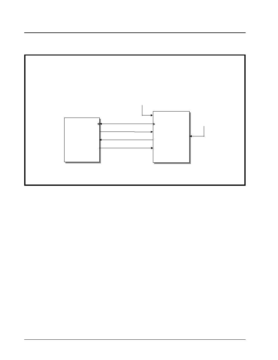
XRT7250
DS3/E3 FRAMER IC
·Á
·Á
·Á
·Á
REV. 1.1.1
152
Method 1 Operation of the Terminal Equipment
If the Terminal Equipment intends to insert any over-
head data into the outbound DS3 data stream, (via
the Transmit Overhead Data Input Interface), then it is
expected to do the following.
1. To sample the state of the TxOHFrame signal
(e.g., the Tx_Start_of_Frame input signal) on the
rising edge of the TxOHClk (e.g., the
DS3_OH_Clock_In signal).
2. To keep track of the number of rising clock edges
that have occurred, via the TxOHClk (e.g., the
DS3_OH_Clock_In signal) since the last time the
TxOHFrame signal was sampled "High". By
doing this the Terminal Equipment will be able to
keep track of which overhead bit is being pro-
cessed by the Transmit Overhead Data Input
Interface block at any given time. When the Ter-
minal Equipment knows which overhead bit is
being processed, at a given TxOHClk period, it
will know when to insert a desired overhead bit
value into the outbound DS3 data stream. From
this, the Terminal Equipment will know when it
should assert the TxOHIns input pin and place
the appropriate value on the TxOH input pin (of
the XRT7250).
Table 21relates the number of rising clock edges (in
the TxOHClk signal, since TxOHFrame was sampled
"High") to the DS3 Overhead Bit, that is being pro-
cessed.
F
IGURE
57. I
LLUSTRATION
OF
THE
T
ERMINAL
E
QUIPMENT
BEING
INTERFACED
TO
THE
T
RANSMIT
O
VERHEAD
D
ATA
I
NPUT
I
NTERFACE
(M
ETHOD
1)
Terminal Equipment
XRT7250 DS3 Framer
DS3_OH_Out]
DS3_OH_Clock_In
Tx_Start_of_Frame
TxOHClk
TxOHFrame
TxOHIns
44.736 MHz Clock Source
TxInClk
TxOH
Insert_OH
RxLineClk
44.736 MHz
Clock Source

·Á
·Á
·Á
·Á
DS3/E3 FRAMER IC
XRT7250
REV. 1.1.1
153
T
ABLE
21: T
HE
R
ELATIONSHIP
BETWEEN
THE
N
UMBER
OF
R
ISING
C
LOCK
E
DGES
IN
T
X
OHC
LK
, (
SINCE
T
X
OHF
RAME
WAS
LAST
SAMPLED
"H
IGH
")
TO
THE
DS3 O
VERHEAD
B
IT
,
THAT
IS
BEING
PROCESSED
N
UMBER
OF
R
ISING
C
LOCK
E
DGES
IN
T
X
OHC
LK
T
HE
O
VERHEAD
B
IT
E
XPECTED
BY
THE
XRT7250
C
AN
THIS
OVERHEAD
BIT
BE
ACCEPTED
BY
THE
XRT7250?
0 (Clock edge is coincident with TxO-
HFrame being detected "High")
X
Yes
1
F1
No
2
AIC
Yes
3
F0
No
4
NA
Yes
5
F0
No
6
FEAC
Yes
7
F1
No
8
X
Yes
9
F1
No
10
UDL
Yes
11
F0
No
12
UDL
Yes
13
F0
No
14
UDL
Yes
15
F1
No
16
P
No
17
F1
No
18
CP
Yes
19
F0
No
20
CP
Yes
21
F0
No
22
CP
Yes
23
F1
No
24
P
No
25
F1
No
26
FEBE
Yes
27
F0
No
28
FEBE
Yes
29
F0
No
30
FEBE
Yes
31
F1
No
32
M0
No
33
F1
No
34
DL
Yes
35
F0
No
36
DL
Yes
37
F0
No

XRT7250
DS3/E3 FRAMER IC
·Á
·Á
·Á
·Á
REV. 1.1.1
154
3. After the Terminal Equipment has waited the
appropriate number of clock edges (from the
TxOHFrame signal being sampled "High"), it
should assert the TxOHIns input signal. Concur-
rently, the Terminal Equipment should also place
the appropriate value (of the inserted overhead
bit) onto the TxOH signal.
4. The Terminal Equipment should hold both the
TxOHIns input pin "High" and the value of the
TxOH signal, stable until the next rising edge of
TxOHClk is detected.
Case Study: The Terminal Equipment intends to
insert the appropriate overhead bits into the
Transmit Overhead Data Input Interface (using
Method 1) in order to transmit a Yellow Alarm to
the remote terminal equipment.
In this example, the Terminal Equipment intends to in-
sert the appropriate overhead bits, into the Transmit
Overhead Data Input Interface, such that the
XRT7250 will transmit a Yellow Alarm to the remote
terminal equipment. Recall that, for DS3 Applica-
tions, a Yellow Alarm is transmitted by setting both of
the X bits (within each outbound DS3 frame) to 0.
If one assumes that the connection between the Ter-
minal Equipment and the XRT7250 are as illustrated
in Figure 57 then Figure 58 presents an illustration of
the signaling that must go on between the Terminal
Equipment and the XRT7250.
38
DL
Yes
39
F1
No
40
M1
No
41
F1
No
42
UDL
Yes
43
FO
No
44
UDL
Yes
45
FO
No
46
UDL
Yes
47
F1
No
48
M0
No
49
F1
No
50
UDL
Yes
51
F0
No
52
UDL
Yes
53
F0
No
54
UDL
Yes
55
F1
No
T
ABLE
21: T
HE
R
ELATIONSHIP
BETWEEN
THE
N
UMBER
OF
R
ISING
C
LOCK
E
DGES
IN
T
X
OHC
LK
, (
SINCE
T
X
OHF
RAME
WAS
LAST
SAMPLED
"H
IGH
")
TO
THE
DS3 O
VERHEAD
B
IT
,
THAT
IS
BEING
PROCESSED
N
UMBER
OF
R
ISING
C
LOCK
E
DGES
IN
T
X
OHC
LK
T
HE
O
VERHEAD
B
IT
E
XPECTED
BY
THE
XRT7250
C
AN
THIS
OVERHEAD
BIT
BE
ACCEPTED
BY
THE
XRT7250?
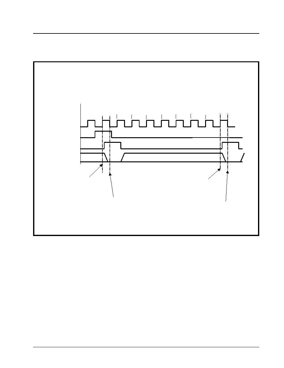
·Á
·Á
·Á
·Á
DS3/E3 FRAMER IC
XRT7250
REV. 1.1.1
155
In Figure 58 the Terminal Equipment samples the Tx-
OHFrame signal being "High" at the rising clock edge
# 0. At this point, the Terminal Equipment knows that
the XRT7250 is just about to process the very first
overhead bit within a given outbound DS3 frame. Ad-
ditionally, according to Table 21, the very first over-
head bit to be processed is the first X bit. In order to
facilitate the transmission of the Yellow Alarm, the
Terminal Equipment must set this X bit to 0. Hence,
the Terminal Equipment starts this process by imple-
menting the following steps concurrently.
a. Assert the TxOHIns input pin by setting it "High".
b. Set the TxOH input pin to 0.
After the Terminal Equipment has applied these sig-
nals, the XRT7250 will sample the data on both the
TxOHIns and TxOH signals upon the very next falling
edge of TxOHClk (designated at 0- in Figure 58.
Once the XRT7250 has sampled this data, it will then
insert a "0" into the first X bit position, in the outbound
DS3 frame.
Upon detection of the very next rising edge of the Tx-
OHClk clock signal (designated as clock edge 1 in
Figure 58), the Terminal Equipment will negate the
TxOHIns signal (e.g., toggles it "Low") and will cease
inserting data into the Transmit Overhead Data Input
Interface, until rising clock edge # 8 (of the TxOHClk
signal). According to Table 21, rising clock edge # 8
indicates that the XRT7250 is just about ready to pro-
cess the second X bit within the outbound DS3 frame.
Once again, in order to facilitate the transmission of
the Yellow Alarm this X-Bit must also be set to 0.
Hence, the Terminal Equipment will (once again) im-
plement the following steps, concurrently.
a. Assert the TxOHIns input pin by setting it "High".
F
IGURE
58. I
LLUSTRATION
OF
THE
SIGNAL
THAT
MUST
OCCUR
BETWEEN
THE
T
ERMINAL
E
QUIPMENT
AND
THE
XRT7250,
IN
ORDER
TO
CONFIGURE
THE
XRT7250
TO
TRANSMIT
A
Y
ELLOW
A
LARM
TO
THE
REMOTE
TERMINAL
EQUIPMENT
Terminal Equipment/XRT7250 Interface Signals
TxOHClk
TxOHIns
TxOHFrame
TxOH
Remaining Overhead Bits with DS3 Frame
X bit = 0
X bit = 0
TxOHFrame is sample "high"
Terminal Equipment asserts
"TxOHIns" and data on "TxOH" line
XRT7250 device samples the TxOHIns and
TxOH signals.
TxOHFrame is sample "high"
Terminal Equipment asserts
"TxOHIns" and data on "TxOH" line
XRT7250 device samples the TxOHIns and
TxOH signals.
0 0- 1 2 3 4 5 6 7 8 8-

XRT7250
DS3/E3 FRAMER IC
·Á
·Á
·Á
·Á
REV. 1.1.1
156
b. Set the TxOH input to 0.
Once again, after the Terminal Equipment has ap-
plied these signals, the XRT7250 will sample the data
on both the TxOHIns and TxOH signal upon the very
next falling edge of TxOHClk (designated as 8- in
Figure 58). Once the XRT7250 has sampled this da-
ta, it will then insert a "0" into the second X bit posi-
tion, in the outbound DS3 frame.
4.2.2.2
Method 2 - Using the TxInClk and TxO-
HEnable Signals
Method 1 requires the use of an additional clock sig-
nal, TxOHClk. However, there may be a situation in
which the user does not wish to accommodate and
process this extra clock signal to their design, in order
to use the Transmit Overhead Data Input Interface.
Hence, Method 2 is available. When using Method 2,
either the TxInClk or RxOutClk signal is used to sam-
ple the overhead bits and signals which are input to
the Transmit Overhead Data Input Interface. Method
2 involves the use of the following signals:
∑ TxOH
∑ TxInClk
∑ TxOHFrame
∑ TxOHEnable
Each of these signals are listed and described in
Table 22.
Interfacing the Transmit Overhead Data Input Interface
to the Terminal Equipment
Figure 59 illustrates how one should interface the
Transmit Overhead Data Input Interface to the Termi-
nal Equipment when using Method 2.
T
ABLE
22: D
ESCRIPTION
OF
M
ETHOD
2 T
RANSMIT
O
VERHEAD
I
NPUT
I
NTERFACE
S
IGNALS
N
AME
T
YPE
D
ESCRIPTION
TxOHEnable
Output
Transmit Overhead Data Enable Output pin
The XRT7250 will assert this signal, for one TxInClk period, just prior to the instant that
the Transmit Overhead Data Input Interface is processing an overhead bit.
TxOHFrame
Output
Transmit Overhead Input Interface Frame Boundary Indicator Output:
This output signal pulses "High" when the XRT7250 is processing the last bit within a
given DS3 frame.
TxOHIns
Input
Transmit Overhead Data Insert Enable input pin.
Asserting this input signal (e.g., setting it "High") enables the Transmit Overhead Data Input Inter-
face to accept overhead data from the Terminal Equipment. In other words, while this input pin is
"High", the Transmit Overhead Data Input Interface will sample the data at the TxOH input pin, on
the falling edge of the TxInClk output signal.
Conversely, setting this pin "Low" configures the Transmit Overhead Data Input Interface to NOT
sample (e.g., ignore) the data at the TxOH input pin, on the falling edge of the TxOHClk output
signal.
N
OTE
: If the Terminal Equipment attempts to insert an overhead bit that cannot be accepted by
the Transmit Overhead Data Input Interface (e.g., if the Terminal Equipment asserts the TxOHIns
signal, at a time when one of these non-insertable overhead bits are being processed), that par-
ticular insertion effort will be ignored.
TxOH
Input
Transmit Overhead Data Input pin:
The Transmit Overhead Data Input Interface accepts the overhead data via this input
pin, and inserts into the overhead bit position within the very next outbound DS3 frame.
If the TxOHIns pin is pulled "High", the Transmit Overhead Data Input Interface will sam-
ple the data at this input pin (TxOH), on the falling edge of the TxOHClk output pin.
Conversely, if the TxOHIns pin is pulled "Low", then the Transmit Overhead Data Input
Interface will NOT sample the data at this input pin (TxOH). Consequently, this data will
be ignored.
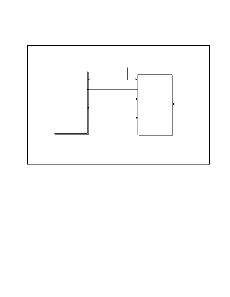
·Á
·Á
·Á
·Á
DS3/E3 FRAMER IC
XRT7250
REV. 1.1.1
157
Method 2 Operation of the Terminal Equipment
If the Terminal Equipment intends to insert any over-
head data into the outbound DS3 data stream (via the
Transmit Overhead Data Input Interface), then it is ex-
pected to do the following.
1. To sample the state of both the TxOHFrame and
the TxOHEnable input signals, via the
DS3_Clock_In (e.g., either the TxInClk or the
RxOutClk signal of the XRT7250) signal. If the
Terminal Equipment samples the TxOHEnable
signal "High", then it knows that the XRT7250 is
about to process an overhead bit. Further, if the
Terminal Equipment samples both the TxO-
HFrame and the TxOHEnable pins "High" (at the
same time) then the Terminal Equipment knows
that the XRT7250 is about to process the first
overhead bit, within a new DS3 frame.
2. To keep track of the number of times that the
TxOHEnable signal has been sampled "High"
since the last time both the TxOHFrame and the
TxOHEnable signals were sampled "High". By
doing this, the Terminal Equipment will be able to
keep track of which overhead bit the Transmit
Overhead Data Input Interface is about ready to
process. From this, the Terminal Equipment will
know when it should assert the TxOHIns input pin
and place the appropriate value on the TxOH
input pins (of the XRT7250).
Table 23 also relates the number of TxOHEnable out-
put pulses (that have occurred since both the TxO-
HFrame and TxOHEnable pins were sampled "High")
to the DS3 overhead bit, that is being processed.
F
IGURE
59. I
LLUSTRATION
OF
THE
T
ERMINAL
E
QUIPMENT
BEING
INTERFACED
TO
THE
T
RANSMIT
O
VERHEAD
D
ATA
I
NPUT
I
NTERFACE
(M
ETHOD
2)
Terminal Equipment
XRT7250 DS3 Framer
DS3_OH_Out
DS3_OH_Enable
Tx_Start_of_Frame
TxOHEnable
TxOHFrame
TxOHIns
44.736 MHz Clock Source
TxInClk
TxOH
Insert_OH
RxLineClk
44.736 MHz
Clock Source
DS3_Clock_In

XRT7250
DS3/E3 FRAMER IC
·Á
·Á
·Á
·Á
REV. 1.1.1
158
T
ABLE
23: T
HE
R
ELATIONSHIP
BETWEEN
THE
N
UMBER
OF
T
X
OHE
NABLE
PULSES
(
SINCE
THE
LAST
OCCURRENCE
OF
THE
T
X
OHF
RAME
PULSE
)
TO
THE
DS3 O
VERHEAD
B
IT
,
THAT
IS
BEING
PROCESSED
BY
THE
XRT7250
N
UMBER
OF
T
X
OHE
NABLE
P
ULSES
T
HE
O
VERHEAD
B
IT
E
XPECTED
BY
THE
XRT7250
C
AN
THIS
OVERHEAD
BIT
BE
ACCEPTED
BY
THE
XRT7250?
0 (The TxOHEnable and TxOHFrame
signals are both sampled "High")
X
Yes
1
F1
No
2
AIC
Yes
3
F0
No
4
NA
Yes
5
F0
No
6
FEAC
Yes
7
F1
No
8
X
Yes
9
F1
No
10
UDL
Yes
11
F0
No
12
UDL
Yes
13
F0
No
14
UDL
Yes
15
F1
No
16
P
No
17
F1
No
18
CP
Yes
19
F0
No
20
CP
Yes
21
F0
No
22
CP
Yes
23
F1
No
24
P
No
25
F1
No
26
FEBE
Yes
27
F0
No
28
FEBE
Yes
29
F0
No
30
FEBE
Yes
31
F1
No
32
M0
No
33
F1
No
34
DL
Yes
35
F0
No
36
DL
Yes
37
F0
No

·Á
·Á
·Á
·Á
DS3/E3 FRAMER IC
XRT7250
REV. 1.1.1
159
3. After the Terminal Equipment has waited through
the appropriate number of pulses via the TxO-
HEnable pin, it should then assert the TxOHIns
input signal. Concurrently, the Terminal Equip-
ment should also place the appropriate value (of
the inserted overhead bit) onto the TxOH signal.
4. The Terminal Equipment should hold both the
TxOHIns input pin "High" and the value of the
TxOH signal stable, until the next TxOHEnable
pulse is detected.
Case Study: The Terminal Equipment intends to
insert the appropriate overhead bits into the
Transmit Overhead Data Input Interface (using
Method 2) in order to transmit a Yellow Alarm to
the remote terminal equipment.
In this case, the Terminal Equipment intends to insert
the appropriate overhead bits, into the Transmit Over-
head Data Input Interface such that the XRT7250 will
transmit a Yellow Alarm to the remote terminal equip-
ment. Recall that, for DS3 applications, a Yellow
Alarm is transmitted by setting all of the X bits to 0.
If one assumes that the connection between the Ter-
minal Equipment and the XRT7250 is as illustrated in
Figure 59 then, Figure 60 presents an illustration of
the signaling that must go on between the Terminal
Equipment and the XRT7250.
38
DL
Yes
39
F1
No
40
M1
No
41
F1
No
42
UDL
Yes
43
FO
No
44
UDL
Yes
45
FO
No
46
UDL
Yes
47
F1
No
48
M0
No
49
F1
No
50
UDL
Yes
51
F0
No
52
UDL
Yes
53
F0
No
54
UDL
Yes
55
F1
No
T
ABLE
23: T
HE
R
ELATIONSHIP
BETWEEN
THE
N
UMBER
OF
T
X
OHE
NABLE
PULSES
(
SINCE
THE
LAST
OCCURRENCE
OF
THE
T
X
OHF
RAME
PULSE
)
TO
THE
DS3 O
VERHEAD
B
IT
,
THAT
IS
BEING
PROCESSED
BY
THE
XRT7250
N
UMBER
OF
T
X
OHE
NABLE
P
ULSES
T
HE
O
VERHEAD
B
IT
E
XPECTED
BY
THE
XRT7250
C
AN
THIS
OVERHEAD
BIT
BE
ACCEPTED
BY
THE
XRT7250?
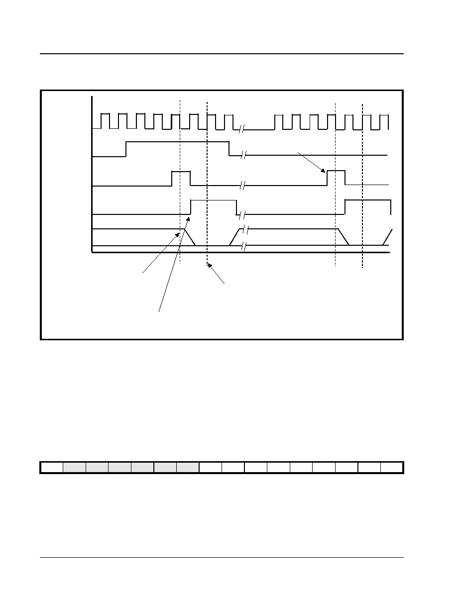
XRT7250
DS3/E3 FRAMER IC
·Á
·Á
·Á
·Á
REV. 1.1.1
160
4.2.3
The Transmit DS3 HDLC Controller
The Transmit DS3 HDLC Controller block can be
used to transport either Bit-Oriented Signaling (BOS)
or Message-Oriented Signaling (MOS) type messag-
es or both types of messages to the remote terminal
equipment. Both BOS and MOS types of HDLC mes-
sage processing are discussed in detail below.
4.2.3.1
Bit-Oriented Signaling (or FEAC Mes-
sage) processing via the Transmit DS3 HDLC
Controller.
The Transmit DS3 HDLC Controller block consists of
two major blocks:
∑ The Transmit FEAC Processor.
∑ The LAPD Transmitter.
This section describes how to operate the Transmit
FEAC Processor. If the Transmit DS3 Framer is oper-
ating in the C-bit Parity Framing Format then the
FEAC (Far-End Alarm & Control) bit-field of the DS3
Frame can be used to transmit the FEAC messages
(See Figure 42). The FEAC code word is a 6-bit val-
ue which is encapsulated by 10 framing bits, forming
a 16-bit FEAC message of the form:
where '[d5, d4, d3, d2, d1, d0]' is the FEAC code
word. The rightmost bit (e.g., a 1) of the FEAC Mes-
sage, is transmitted first. Since each DS3 frame con-
tains only 1 FEAC bit, 16 DS3 Frames are required to
transmit the 16 bit FEAC Code Message.
The XRT7250 contains the following two registers
that support FEAC Message Transmission.
∑ Tx DS3 FEAC Register (Address = 0x32)
∑ Tx DS3 FEAC Configuration and Status Register
(Address = 0x33)
Operating the Transmit FEAC Processor
In order to transmit a FEAC message to the remote
terminal, the user must execute the following steps.
F
IGURE
60. B
EHAVIOR
OF
T
RANSMIT
O
VERHEAD
D
ATA
I
NPUT
I
NTERFACE
SIGNALS
BETWEEN
THE
XRT7250
AND
THE
T
ERMINAL
E
QUIPMENT
(
FOR
M
ETHOD
2)
TxInClk
TxOHFrame
TxOHEnable
TxOHIns
TxOH
Terminal Equipment
samples "TxOHFrame" and
"TxOHEnable" being "HIGH"
Terminal Equipment
responds by asserting
TxOHIns and placing desired
data on TxOH.
XRT7250 samples TxOH
here.
TxOHEnable Pulse # 8
X bit = 0
X bit = 0
0
d5
d4
d3
d2
d1
d0
0
1
1
1
1
1
1
1
1

·Á
·Á
·Á
·Á
DS3/E3 FRAMER IC
XRT7250
REV. 1.1.1
161
1. Write the 6-bit FEAC code (to be sent) into the Tx
DS3 FEAC Register.
2. Enable the Transmit FEAC Processor.
3. Initiate the Transmission of the FEAC Message.
Each of these steps will be described in detail below.
STEP 1 - Writing in the six bit FEAC Codeword (to
be sent)
In this step, the µP/µC writes the six bit FEAC code
word into the Tx DS3 FEAC Register. The bit format
of this register is presented below.
STEP 2 - Enabling the Transmit FEAC Processor
In order to enable the Transmit FEAC Processor
(within the Transmit DS3 HDLC Controller block) the
user must write a 1 into bit 2 (Tx FEAC Enable) within
the Tx DS3 FEAC Configuration and Status Register,
as depicted below.
At this point, the Transmit FEAC Processor can be
commanded to begin transmission (See STEP 3).
STEP 3 - Initiate the Transmission of the FEAC
Message
The user can initiate the transmission of the FEAC
code word (residing in the Tx DS3 FEAC register) by
writing a 1 to bit 1 (Tx FEAC Go) within the Tx DS3
FEAC Configuration and Status register, as depicted
below.
N
OTE
: While executing this particular write operation, the
user should write the binary value 000xx110b into the Tx
DS3 FEAC Configuration and Status Register. By doing
this the user insures that a 1 is also being written to Bit 2
(Tx FEAC Enable) of the register, in order to keep the
Transmit FEAC Processor enabled.
Once this step has been completed, the Transmit
FEAC Processor will proceed to transmit the 16 bit
FEAC code via the outbound DS3 frames. This 16 bit
FEAC message will be transmitted repeatedly 10
consecutive times. Hence, this process will require a
total of 160 DS3 Frames. During this process the Tx
FEAC Busy bit (Bit 0, within the Transmit DS3 FEAC
Configuration and Status register) will be asserted,
indicating that the Tx FEAC Processor is currently
transmitting the FEAC Message to the remote Termi-
nal. This bit-field will toggle to "0" upon completion of
the 10th transmission of the FEAC Code Message.
The Transmit FEAC Processor will generate an inter-
rupt (if enabled) to the local µP/µC, upon completion
of the 10th transmission of the FEAC Message. The
purpose of having the Framer IC generating this inter-
rupt is to let the local µP/µC know that the Transmit
FEAC Processor is now available and ready to trans-
mit a new FEAC message. Finally, once the Transmit
FEAC Processor has completed its 10th transmission
of a FEAC Code Message it will then begin sending
TX DS3 FEAC REGISTER (ADDRESS = 0X32)
B
IT
7
B
IT
6
B
IT
5
B
IT
4
B
IT
3
B
IT
2
B
IT
1
B
IT
0
Not Used
TxFEAC[5]
TxFEAC[4]
TxFEAC[3]
TxFEAC[2]
TxFEAC[1]
TxFEAC[0]
Not Used
RO
R/W
R/W
R/W
R/W
R/W
R/W
R0
0
d5
d4
d3
d2
d1
d0
0
TRANSMIT DS3 FEAC CONFIGURATION AND STATUS REGISTER (ADDRESS = 0X31)
B
IT
7
B
IT
6
B
IT
5
B
IT
4
B
IT
3
B
IT
2
B
IT
1
B
IT
0
Not Used
Not Used
Not Used
TxFEAC
Interrupt
Enable
TxFEAC
Interrupt
Status
TxFEAC
Enable
TxFEAC
Go
TxFEAC
Busy
RO
RO
RO
R/W
RO
R/W
R/W
R0
x
x
x
x
x
1
X
X
TRANSMIT DS3 FEAC CONFIGURATION AND STATUS REGISTER (ADDRESS = 0X31)
B
IT
7
B
IT
6
B
IT
5
B
IT
4
B
IT
3
B
IT
2
B
IT
1
B
IT
0
Not Used
Not Used
Not Used
TxFEAC
Interrupt
Enable
TxFEAC
Interrupt
Status
TxFEAC
Enable
TxFEAC
Go
TxFEAC
Busy
RO
RO
RO
R/W
RO
R/W
R/W
R0
x
x
x
x
x
1
1
X

XRT7250
DS3/E3 FRAMER IC
·Á
·Á
·Á
·Á
REV. 1.1.1
162
all 1s in the FEAC bit-field of each DS3 Frame. The
Receive FEAC Processor (at the remote terminal
equipment) will interpret this all 1s message as an
Idle FEAC Message. The Transmit FEAC Processor
will continue sending all 1s in the FEAC bit field, for
an indefinite period of time, until the local µP/µC com-
mands it to transmit a new FEAC message.
Figure 61 presents a flow chart depicting how to use
the Transmit FEAC Processor.
For a detailed description of the Receive FEAC Pro-
cessor (within the Receive DS3 HDLC Controller
block), please see Section 3.3.3.1.
4.2.3.2
Message-Oriented Signaling (e.g.,
LAP-D) processing via the Transmit DS3 HDLC
Controller
The LAPD Transmitter (within the Transmit DS3
HDLC Controller Block) allows the user to transmit
path maintenance data link (PMDL) messages to the
remote terminal via the outbound DS3 Frames. In
this case the message bits are inserted into and car-
ried by the 3 DL bit fields of F-Frame #5 within each
DS3 M-frame. The on-chip LAPD transmitter sup-
ports both the 76 byte and 82 byte length message
formats, and the Framer IC allocates 88 bytes of on-
chip RAM (e.g., the Transmit LAPD Message buffer)
to store the message to be transmitted. The mes-
sage format complies with ITU-T Q.921 (LAP-D) pro-
tocol with different addresses and is presented below
in Figure 62.
F
IGURE
61. A F
LOW
C
HART
DEPICTING
HOW
TO
TRANSMIT
A
FEAC M
ESSAGE
VIA
THE
FEAC T
RANSMITTER
START
START
WRITE SIX-BIT "OUTBOUND" FEAC VALUE
INTO THE TxDS3 FEAC Register
This register is located at Address 0x32.
WRITE SIX-BIT "OUTBOUND" FEAC VALUE
INTO THE TxDS3 FEAC Register
This register is located at Address 0x32.
ENABLE THE TRANSMIT FEAC PROCESSOR.
This is accomplished by writing "xxxx x1xx"
into the TxDS3 FEAC Configuration & Status Register
ENABLE THE TRANSMIT FEAC PROCESSOR.
This is accomplished by writing "xxxx x1xx"
into the TxDS3 FEAC Configuration & Status Register
INITIATE TRANSMISSION OF THE "OUTBOUND"
FEAC MESSAGE.
This is accomplished by writing "xxxx xx1x" into the
TxDS3 FEAC Configuration & Status Register.
INITIATE TRANSMISSION OF THE "OUTBOUND"
FEAC MESSAGE.
This is accomplished by writing "xxxx xx1x" into the
TxDS3 FEAC Configuration & Status Register.
TRANSMIT FEAC PROCESSOR ENCAPSULATES
THE "OUTBOUND" FEAC VALUE INTO A 16 BIT
FRAMING STRUCTURE.
TRANSMIT FEAC PROCESSOR ENCAPSULATES
THE "OUTBOUND" FEAC VALUE INTO A 16 BIT
FRAMING STRUCTURE.
TRANSMIT FEAC PROCESSOR PROCEEDS TO
INSERT THE 16-BIT MESSAGE (IN A BIT-BY-BIT
MANNER) INTO THE "FEAC" BIT-FIELDS OF
EACH OUTBOUND DS3 FRAME.
TRANSMIT FEAC PROCESSOR PROCEEDS TO
INSERT THE 16-BIT MESSAGE (IN A BIT-BY-BIT
MANNER) INTO THE "FEAC" BIT-FIELDS OF
EACH OUTBOUND DS3 FRAME.
Is
Transmission
of the 16 Bit FEAC
Message
Complete
?
Is
Transmission
of the 16 Bit FEAC
Message
Complete
?
Has
the 16-bit
FEAC Message been
transmitted to the
Remote Terminal
10 times
?
Has
the 16-bit
FEAC Message been
transmitted to the
Remote Terminal
10 times
?
GENERATE THE TRANSMIT FEAC
INTERRUPT
GENERATE THE TRANSMIT FEAC
INTERRUPT
INVOKE THE "TRANSMIT FEAC INTERRUPT
SERVICE ROUTINE.
INVOKE THE "TRANSMIT FEAC INTERRUPT
SERVICE ROUTINE.
1
1
1
1
NO
YES
NO
YES
·Á
·Á
·Á
·Á
DS3/E3 FRAMER IC
XRT7250
REV. 1.1.1
163
Where: Flag Sequence = 0x7E
SAPI + CR + EA = 0x3C or 0x3E
TEI + EA = 0x01
Control = 0x03
The following sections defines each of these bit/byte-
fields within the LAPD Message Frame Format.
Flag Sequence Byte
The Flag Sequence byte is of the value 0x7E, and is
used to for two purposes
1. To denote the boundaries of the LAPD Message
Frame, and
2. To function as the Idle Pattern (e.g., Transmit
HDLC Controller block transmits a continuous
stream of flag sequence octets, whenever no
LAPD Message is being transmitted).
SAPI - Service Access Point Identifier
The SAPI bit-fields are assigned the value of
001111b or 15 (decimal).
TEI - Terminal Endpoint Identifier
The TEI bit-fields are assigned the value of 0x00.
The TEI field is used in N-ISDN systems to identify a
terminal out of multiple possible terminal. However,
since the Framer IC transmits data in a point-to-point
manner, the TEI value is unimportant.
Control
The Control identifies the type of frame being trans-
mitted. There are three general types of frame for-
mats: Information, Supervisory, and Unnumbered.
The Framer assigned the Control byte the value 0x03.
Hence, the Framer will be transmitting and receiving
Unnumbered LAPD Message frames.
Information Payload
The Information Payload is the 76 bytes or 82 bytes of
data (e.g., the PMDL Message) that the user has writ-
ten into the on-chip Transmit LAPD Message buffer
(which is located at addresses 0x86 through 0xDD).
It is important to note that the user must write in a
specific octet value into the first byte position within
the Transmit LAPD Message buffer (located at Ad-
dress = 0x86, within the Framer). The value of this
octet depends upon the type of LAPD Message
frame/PMDL Message that the user wishes to trans-
mit. Table 24 presents a list of the various types of
LAPD Message frames/PMDL Messages that are
supported by the XRT7250 Framer and the corre-
sponding octet value that the user must write into the
first octet position within the Transmit LAPD Message
buffer.
Frame Check Sequence Bytes
F
IGURE
62. LAPD M
ESSAGE
F
RAME
F
ORMAT
Flag Sequence (8 bits)
SAPI (6-bits)
C/R
EA
TEI (7 bits)
EA
Control (8-bits)
76 or 82 Bytes of Information (Payload)
FCS - MSB
FCS - LSB
Flag Sequence (8-bits)
T
ABLE
24: T
HE
LAPD M
ESSAGE
T
YPE
AND
THE
C
ORRESPONDING
VALUE
OF
THE
F
IRST
B
YTE
,
WITHIN
THE
I
NFORMATION
P
AYLOAD
LAPD M
ESSAGE
T
YPE
V
ALUE
OF
F
IRST
B
YTE
,
WITHIN
I
NFORMATION
P
AYLOAD
OF
M
ESSAGE
M
ESSAGE
S
IZE
CL Path Identification
0x38
76 bytes
IDLE Signal Identification
0x34
76 bytes
Test Signal Identification
0x32
76 bytes
ITU-T Path Identification
0x3F
82 bytes
XRT7250
DS3/E3 FRAMER IC
·Á
·Á
·Á
·Á
REV. 1.1.1
164
The 16 bit FCS (Frame Check Sequence) is calculat-
ed over the LAPD Message Header and Information
Payload bytes, by using the CRC-16 polynomial, x
16
+ x
12
+ x
5
+ 1.
Operation of the LAPD Transmitter
If a message is to be transmitted via the LAPD Trans-
mitter, the information portion (or the body) of the
message must be written into the Transmit LAPD
Message Buffer, which is located at 0x86 through
0xDD in on-chip RAM via the Microprocessor Inter-
face. Afterwards, the user must do three things:
1. Specify the length of LAPD message to be trans-
mitted.
2. Enable the LAPD Transmitter.
3. Initiate the Transmission of the PMDL Message.
Each of these steps will be discussed in detail.
STEP 1 - Specifying the Length of the LAPD Mes-
sage
One of two different sizes of LAPD Messages can be
transmitted. This is accomplish by writing the appro-
priate data to bit 1 within the Tx DS3 LAPD Configu-
ration Register. The bit-format of this register is pre-
sented below.
The relationship between the contents of bit-fields 1
and the LAPD Message size is given in Table 25.
N
OTE
: The Message Type selected must correspond with
the contents of the first byte of the Information (Payload)
portion, as presented in Table 24.
STEP 2 - Enabling the LAPD Transmitter
Prior to the transmission of any data via the LAPD
Transmitter the LAPD Transmitter must be enabled.
This is accomplish this by writing a 1 to bit 0 of the Tx
DS3 LAPD Configuration Register, as depicted be-
low.
Bit 0 - TxLAPD Enable
This bit-field allow the user to enable or disable the
LAPD Transmitter in accordance with Table 26.
TRANSMIT DS3 LAPD CONFIGURATION REGISTER (ADDRESS = 0X33)
B
IT
7
B
IT
6
B
IT
5
B
IT
4
B
IT
3
B
IT
2
B
IT
1
B
IT
0
Not Used
Auto
Retransmit
Not Used
TxLAPD
Msg Length
TxLAPD
Enable
R/O
R/O
R/O
R/O
R/W
R/O
R/W
R/W
0
0
0
0
X
0
X
X
T
ABLE
25: R
ELATIONSHIP
BETWEEN
T
X
LAPD M
SG
L
ENGTH
AND
THE
LAPD M
ESSAGE
S
IZE
T
X
LAPD M
SG
L
ENGTH
LAPD M
ESSAGE
L
ENGTH
0
LAPD Message size is 76 bytes
1
LAPD Message size is 82 bytes
TRANSMIT DS3 LAPD CONFIGURATION REGISTER (ADDRESS = 0X33)
B
IT
7
B
IT
6
B
IT
5
B
IT
4
B
IT
3
B
IT
2
B
IT
1
B
IT
0
Not Used
Auto
Retransmit
Not Used
TxLAPD
Msg Length
TxLAPD
Enable
R/O
R/O
R/O
R/O
R/W
R/O
R/W
R/W
0
0
0
0
X
0
X
1
T
ABLE
26: R
ELATIONSHIP
BETWEEN
T
X
LAPD M
SG
L
ENGTH
AND
THE
LAPD M
ESSAGE
S
IZE
T
X
LAPD E
NABLE
R
ESULTING
A
CTION
OF
THE
LAPD T
RANSMITTER
0
The LAPD Transmitter is disabled and the DL bits, in the DS3 frame,
are transmitted as all 1s.
1
The LAPD Transmitter is enabled and is transmitting a continuous
stream of Flag Sequence octets (0x7E).

·Á
·Á
·Á
·Á
DS3/E3 FRAMER IC
XRT7250
REV. 1.1.1
165
Prior to executing step 2 (Enabling the LAPD Trans-
mitter), the LAPD Transmitter will be disabled and the
Transmit DS3 Framer block will be setting each of the
DL bits (within the outbound DS3 data stream) to 1.
After the user executes this step, the LAPD Transmit-
ter will begin transmitting the flag sequence octet
(0x7E) via the DL bits.
N
OTE
: Upon power up or reset, the LAPD Transmitter is
disabled. Therefore, the user must set this bit to "1" in order
to enable the LAPD Transmitter.
STEP 3 - Initiate the Transmission
At this point, the LAPD Transmitter is ready to begin
transmission. The user has written the information
portion of the PMDL message into the on-chip Trans-
mit LAPD Message buffer. Further, the user has
specified the type of LAPD message that he/she
wishes to transmit, and has enabled the LAPD Trans-
mitter. The only thing remaining to do is to initiate the
transmission of this message. The user initiates this
process by writing a "1" to Bit 3 of the Tx DS3 LAPD
Status/Interrupt Register (TxDL Start). The bit format
of this register is presented below.
A "0" to "1" transition of Bit 3 (TxDL Start) in this reg-
ister, initiates the transmission of the data link mes-
sage. While the LAPD transmitter is transmitting the
message, the 'TxDL Busy' (bit 2) bit will be set to 1.
This bit-field allows the user to poll the status of the
LAPD Transmitter. Once the message transfer is
completed, this bit-field will toggle back to '0'.
The user can configure the LAPD Transmitter to inter-
rupt the µC/µP upon completion of transmission of
the LAPD Message, by setting bit-field "1" (TxLAPD
Interrupt Enable) of the Tx DS3 LAPD Status/Inter-
rupt register to 1. The purpose of this interrupt is to let
the local µC/µP know that the LAPD Transmitter is
available and ready to transmit a new message. Bit 0
will reflect the interrupt status for the LAPD Transmit-
ter.
N
OTE
: This bit-field will be reset on reading this register.
Details Associated with the Transmission of a
PMDL Message
Once the user has invoked the TxDL Start command,
the LAPD Transmitter will do the following.
∑ Generate the four octets of LAPD frame header
(e.g., Flag Sequence, SAPI, TEI, Control, etc.) and
insert it into the LAPD Message, prior to the user's
information (see the LAPD Message Frame Format
in Figure 62).
∑ Compute the 16 bit Frame Check Sum (FCS) of the
LAPD Message Frame (e.g., of the LAPD Message
header and information payload) and append this
value to the LAPD Message.
∑ Append a trailer Flag Sequence octet to the end of
the message LAPD (following the 16 bit FCS
value).
∑ Serialize the composite LAPD message and begin
inserting the LAPD message into the DL bit fields of
each outgoing DS3 Frame.
∑ Complete the transmission of the frame overhead,
payload, FCS value, and trailer Flag Sequence
octet via the Transmit DS3 Framer.
Once the LAPD Transmitter has completed its trans-
mission of the LAPD Message, the Framer will gener-
ate an interrupt to the local µC/µP (if enabled). After-
wards, the LAPD Transmitter will proceed to retrans-
mit the LAPD Message, repeatedly at one second in-
tervals. During Idle periods (e.g., in between these
transmission of the LAPD Message), the LAPD
Transmitter will be sending a continuous stream of
Flag Sequence Bytes. The LAPD Transmitter will
continue this behavior until the user has disabled the
LAPD Transmitter by writing a "0" to bit 0 (TxLAPD
Enable) within the Tx DS3 LAPD Configuration Reg-
ister. If the LAPD Transmitter is idle, then it will con-
tinuously send the Flag Sequence octets (via the DL
bits of each outbound DS3 Frame) to the remote ter-
minal equipment.
N
OTE
: In order to prevent the user's data (e.g., the payload
portion of the LAPD Message Frame) from mimicking the
Flag Sequence byte, the LAPD Transmitter will insert a "0"
into the LAPD data stream immediately following the detec-
tion of five (5) consecutive 1s (this stuffing occurs only while
the information payload is being transmitted). The 'remote'
LAPD Receiver (see Section 4.3.3.2) will have the responsi-
bility of detecting the 5 consecutive 1s and removing the
TRANSMIT DS3 LAPD STATUS/INTERRUPT REGISTER (ADDRESS = 0X34)
B
IT
7
B
IT
6
B
IT
5
B
IT
4
B
IT
3
B
IT
2
B
IT
1
B
IT
0
Not Used
Tx DL
Start
Tx DL
Busy
TxLAPD
Interrupt
Enable
TxLAPD
Interrupt
Status
R/O
R/O
R/O
R/O
R/W
RO
R/W
RUR
0
0
0
0
1
X
X
X
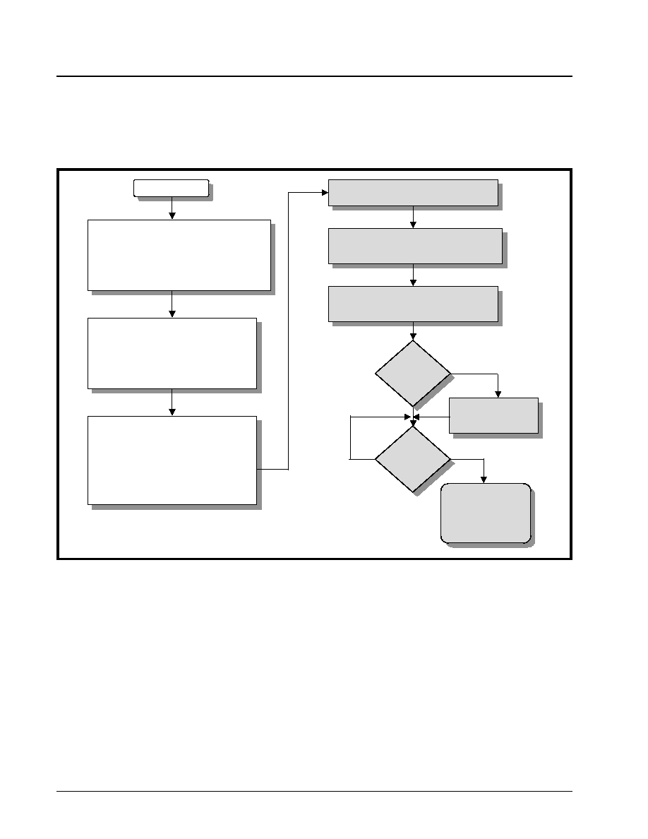
XRT7250
DS3/E3 FRAMER IC
·Á
·Á
·Á
·Á
REV. 1.1.1
166
subsequent "0" from the payload portion of the incoming
LAPD message.
Figure 63 presents a flow chart depicting the proce-
dure (in 'white boxes') that the user should use in or-
der to transmit a LAPD message. This figure also in-
dicates (via the shaded boxes) what the LAPD Trans-
mitter circuitry will do before and during message
transmission.
The Mechanics of Transmitting a New LAPD Mes-
sage
As mentioned above, after the LAPD Transmitter has
been enabled, and commanded to transmit the mes-
sage, residing in the Transmit LAPD Message buffer,
it will continue to transmit this message at one-sec-
ond intervals. If another (e.g., different) PMDL mes-
sage is to be transmitted to the Remote LAPD Re-
ceiver, the new message will have to be written into
the Transmit LAPD Message buffer, via the Micropro-
cessor Interface section of the Framer. However,
care must be taken when writing in this new mes-
sage. If this message is written into the Transmit
LAPD Message buffer at the wrong time (with respect
to these one-second transmissions), the user's action
could interfere with these transmissions, thereby
causing the LAPD Transmitter to transmit a corrupted
message to the Remote LAPD Receiver. In order to
avoid this problem, while writing the new message in-
to the Transmit LAPD Message buffer, the user
should do the following:
1. Configure the Framer to automatically reset acti-
vated interrupts
This can be done by writing a "1" into Bit 3 of the
Framer Operating Mode Register, as depicted below.
F
IGURE
63. F
LOW
C
HART
DEPICT
HOW
TO
USE
THE
LAPD T
RANSMITTER
START
START
WRITE IN DATA LINK INFORMATION
The user accomplishes this by writing the
information that he/she wishes to transmit
(via the LAPD Transmitter) to locations 0x86
through 0xDD, within the Framer Address Space.
ENABLE THE LAPD
TRANSMITTER FOR TRANSMISSION
This is accomplished by writing 00000xx1b
to the Tx DS3 LAPD Configuration Register.
(where xx dictates LAPD Message Length)
INITIATE TRANSMISSION OF LAPD
MESSAGE
This is accomplished by writing 000010x0b
to the Tx DS3 LAPD Status/Interrupt
Register. (where x indicates the user's choice
to enable/disable "LAPD Message Transfer
Complete" Interrupt
LAPD Transmitter inserts Frame Header
octets in front of the user payload.
LAPD Transmitter computes the 16 bit FCS
(a CRC-16 value) and inserts it into the LAPD
Message, following the user payload
LAPD Transmitter appends a Flag Sequence
Trailer octet to the end of the LAPD Message
(after the 16 bit FCS).
Is
5 consecutive
"1s" detected
?
Is
Message
Transmission
Complete
?
Insert a "0" after the
string of 5 consecutive
"1s"
END
Generate Interrupt
LAPD Transmitter will
continue to transmit
Flag Sequence octets.
Yes
No
Yes
No
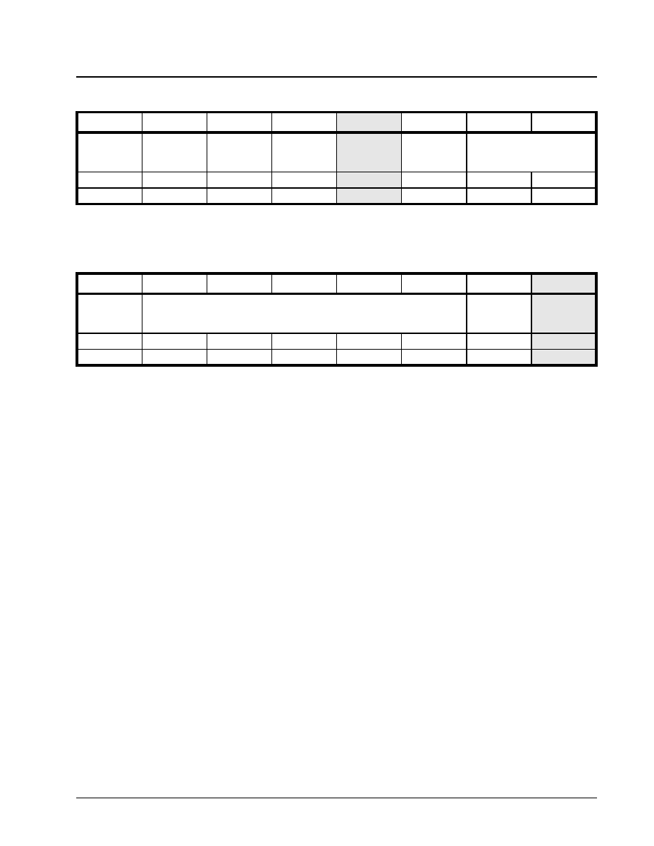
·Á
·Á
·Á
·Á
DS3/E3 FRAMER IC
XRT7250
REV. 1.1.1
167
This action will prevent the LAPD Transmitter from
generating its own one-second interrupts.
2. Enable the One-Second Interrupt
This can be done by writing a "1" into Bit 0 of the
Block Interrupt Enable Register, as depicted below.
3. Write the new message into the Transmit LAPD
Message buffer immediately after the occurrence
of the One-Second interrupt.
By timing the writes to the Transmit LAPD Message
buffer to occur immediately after the occurrence of
the One-Second interrupt, the user avoids conflicting
with the one-second transmissions of the LAPD Mes-
sage, and will transmit the correct messages to the
remote LAPD Receiver.
4.2.4
The Transmit DS3 Framer Block
4.2.4.1
Brief Description of the Transmit DS3
Framer
The Transmit DS3 Framer block accepts data from
any of the following three sources, and uses it to form
the DS3 data stream.
∑ The Transmit Payload Data Input block
∑ The Transmit Overhead Data Input block
∑ The Transmit HDLC Controller block
∑ The Internal Overhead Data Generator
The manner in how the Transmit DS3 Framer block
handles data from each of these sources is described
below.
Handling of data from the Transmit Payload Data
Input Interface
For DS3 applications, all data that is input to the
Transmit Payload Data Input Interface will be inserted
into the payload bit positions within the outbound DS3
frames.
Handling of data from the Internal Overhead Bit
Generator
By default, the Transmit DS3 Framer block will inter-
nally generate the overhead bits. However, if the Ter-
minal Equipment inserts its own values for the over-
head bits (via the Transmit Overhead Data Input Inter-
face) or, if the user enables and employs the Transmit
DS3 HDLC Controller block, then these internally
generated overhead bits will be overwritten.
Handling of data from the Transmit Overhead Da-
ta Input Interface
For DS3 applications, the Transmit DS3 Framer block
automatically generates and inserts the framing align-
ment bits (e.g., the F and M bits) into the outbound
DS3 frames. Further, the Transmit DS3 Framer block
will automatically compute and insert the P-bits into
the outbound DS3 frames. Hence, the Transmit DS3
Framer block will not accept data from the Transmit
OH Data Input Interface block for the F, M and P bits.
However, the Transmit DS3 Framer block will accept
(and insert) data from the Transmit Overhead Data In-
put Interface for the following bit-fields.
∑ X-bits
∑ FEBE bits
∑ FEAC bits
∑ DL bits
∑ UDL bits
∑ CP bits
FRAMER OPERATING MODE REGISTER (ADDRESS = 0X00)
B
IT
7
B
IT
6
B
IT
5
B
IT
4
B
IT
3
B
IT
2
B
IT
1
B
IT
0
Local Loop-
back
DS3/E3*
Internal
LOS
Enable
RESET
Interrupt
Enable
Reset
Frame
Format
TimRefSel[1:0]
R/W
R/W
R/W
R/W
R/W
R/W
R/W
R/W
0
1
1
0
1
X
X
X
BLOCK INTERRUPT ENABLE REGISTER (ADDRESS = 0X04)
B
IT
7
B
IT
6
B
IT
5
B
IT
4
B
IT
3
B
IT
2
B
IT
1
B
IT
0
RxDS3/E3
Interrupt
Enable
Not Used
TxDS3/E3
Interrupt
Enable
One Second
Interrupt
Enable
R/W
RO
RO
RO
RO
RO
R/W
R/W
0
0
0
0
0
0
0
X
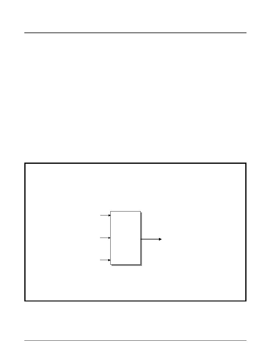
XRT7250
DS3/E3 FRAMER IC
·Á
·Á
·Á
·Á
REV. 1.1.1
168
If the user's local Data Link Equipment activates the
Transmit Overhead Data Input Interface block and
writes data into this interface for these bits, then the
Transmit DS3 Framer block will insert this data into
the appropriate overhead bit-fields, within the out-
bound DS3 frames.
Handling of Data from the Transmit HDLC Con-
troller block
The exact manner in how the Transmit DS3 Framer
handles data from the Transmit HDLC Controller
block depends upon whether the Transmit HDLC
Controller is transmitting BOS (Bit Oriented Signal-
ing) or MOS (Message Oriented Signaling) data.
If the Transmit DS3 HDLC Controller block is not acti-
vated, then the Transmit DS3 Framer block will insert
a "1" into each FEAC and "DL" bit-field, within each
outbound DS3 frame.
If the Transmit DS3 HDLC Controller block is activat-
ed, and is configured to transmit either a "BOS" or
"MOS" type message, then data will be inserted into
the FEAC and "DL" bit-fields as described in Section
3.2.3.
4.2.4.2
Detailed Functional Description of the
Transmit DS3 Framer Block
The Transmit DS3 Framer receives data from the fol-
lowing three sources and combines them together to
form a DS3 data stream.
∑ The Transmit Payload Data Input Interface block.
∑ The Transmit Overhead Data Input Interface block
∑ The Transmit HDLC Controller block.
Afterwards, this DS3 data stream will be routed to the
Transmit DS3 LIU Interface block, for further process-
ing.
Figure 64 presents a simple illustration of the Trans-
mit DS3 Framer block, along with the associated
paths to the other functional blocks within the chip.
In addition to taking data from multiple sources and
multiplexing them, in appropriate manner, to create
the outbound DS3 frames, the Transmit DS3 Framer
block has the following roles.
∑ Generating Alarm Conditions
∑ Generating Errored Frames (for testing purposes)
∑ Routing outbound DS3 frames to the Transmit DS3
LIU Interface block
Each of these additional roles are discussed below.
F
IGURE
64. A S
IMPLE
I
LLUSTRATION
OF
THE
T
RANSMIT
DS3 F
RAMER
B
LOCK
AND
THE
ASSOCIATED
PATHS
TO
OTHER
F
UNCTIONAL
B
LOCKS
Transmit
DS3 Framer
Block
Transmit
DS3 Framer
Block
Transmit HDLC
Controller/Buffer
Transmit Overhead
Data Input Interface
Transmit Payload Data
Input Interface
To Transmit DS3 LIU Interface Block
·Á
·Á
·Á
·Á
DS3/E3 FRAMER IC
XRT7250
REV. 1.1.1
169
4.2.4.2.1
Generating Alarm Conditions
The Transmit DS3 Framer block permits the user to,
by writing the appropriate data into the on-chip regis-
ters, to override the data that is being written into the
Transmit Payload Data and Overhead Data Input In-
terfaces and transmit the following alarm conditions.
∑ Generate the Yellow Alarms (or FERF indicators)
∑ Manipulate the X-bit (set them to 1)
∑ Generate the AIS Pattern
∑ Generate the IDLE pattern
∑ Generate the LOS pattern
∑ Generate FERF (Yellow) Alarms, in response to
detection of a Red Alarm condition (via the Receive
Section of the XRT7250).
∑ Generate and transmit a desired value for FEBE
(Far-End-Block Error).
The procedure and results of generating any of these
alarm conditions is presented below.
The user can exercise each of these options by writ-
ing the appropriate data to the Tx DS3 Configuration
Register (Address = 0x30). The bit format of this reg-
ister is presented below.
The role/function of each of these bit-fields within the
register, are discussed below.
4.2.4.2.1.1
Transmit Yellow Alarm - Bit 7
This read/write bit field permits the user to force the
transmission of a Yellow Alarm to the remote terminal
equipment via software control. If the user opts to
transmit a Yellow Alarm then both of the X-bits, within
the outbound DS3 frames will be set to '0'. Table 27
relates the content of this bit field to the Transmit DS3
Framer block's action.
N
OTE
: This bit is ignored when either the TxIDLE, TxAIS, or
the TxLOS bit-fields are set.
4.2.4.2.1.2
Transmit X-bit - Bit 6
This bit field functions as the logical complement to
Bit 7 (e.g., Tx Yellow Alarm). This read/write bit field
permits the user to force all of the X-bits, in the out-
bound DS3 frames, to "1" and transmit them to the re-
mote terminal equipment. Table 28 relates the con-
tent of this bit field to the Transmit DS3 Framer
Block's action.
TX DS3 CONFIGURATION REGISTER (ADDRESS = 0X30)
B
IT
7
B
IT
6
B
IT
5
B
IT
4
B
IT
3
B
IT
2
B
IT
1
B
IT
0
Tx
Yellow Alarm
Tx X-Bit
Tx IDLE
Pattern
Tx AIS
Pattern
Tx LOS
Pattern
FERF on
LOS
FERF on
OOF
FERF on
AIS
R/W
R/W
R/W
R/W
R/W
R/W
R/W
R/W
0
0
1
0
1
0
1
1
T
ABLE
27: T
HE
R
ELATIONSHIP
BETWEEN
THE
CONTENTS
OF
B
IT
7 (T
X
Y
ELLOW
A
LARM
)
WITHIN
THE
T
X
DS3
C
ONFIGURATION
R
EGISTER
,
AND
THE
RESULTING
T
RANSMIT
DS3 F
RAMER
B
LOCK
'
S
A
CTION
B
IT
7
T
RANSMIT
DS3 F
RAMER
'
S
A
CTION
0
Normal Operation:
The X-bits are generated by the Transmit DS3 Framer block based upon Near End Receiving Conditions (as
detected by the Receive Section of the chip)
1
Transmit Yellow Alarm:
The Transmit DS3 Framer block will overwrite the X-bits by setting them all to 0. The payload information is
not modified and is transmitted as normal.

XRT7250
DS3/E3 FRAMER IC
·Á
·Á
·Á
·Á
REV. 1.1.1
170
N
OTE
: This bit is ignored when either the Transmit Yellow
Alarm, Tx AIS, Tx IDLE, or TxLOS bit is set.
4.2.4.2.1.3
Transmit Idle Pattern - Bit 5
This read/write bit field permits the user to transmit an
Idle pattern to the remote terminal equipment upon
software control. Table 29 relates the contents of this
bit field to the Transmit DS3 Framer's action.
N
OTE
: This bit is ignored when either the Tx AIS or the Tx
LOS bit is set.
4.2.4.2.1.4
Transmit AIS Pattern - Bit 4
This read/write bit field allows the user to transmit an
AIS pattern to the remote terminal equipment, upon
software control. Table 30 relates the contents of this
bit field to the Transmit DS3 Framer block's action.
T
ABLE
28: T
HE
R
ELATIONSHIP
BETWEEN
THE
CONTENTS
OF
B
IT
6 (T
X
X-B
ITS
)
WITHIN
THE
T
X
DS3 C
ONFIGURATION
R
EGISTER
,
AND
THE
RESULTING
T
RANSMIT
DS3 F
RAMER
B
LOCK
'
S
A
CTION
B
IT
6
T
RANSMIT
DS3 F
RAMER
'
S
A
CTION
0
Normal Operation:
The X-bits are generated by the Transmit DS3 Framer block based upon Receiving Conditions (as detected
by the Receive Section of the Framer chip).
1
Set X-bits to 1:
The Transmit DS3 Framer will overwrite the X-bits by setting them to 1. Payload information is not modified
and is transmitted as normal.
T
ABLE
29: T
HE
R
ELATIONSHIP
BETWEEN
THE
CONTENTS
OF
B
IT
5 (T
X
I
DLE
)
WITHIN
THE
T
X
DS3 C
ONFIGURATION
R
EGISTER
,
AND
THE
RESULTING
T
RANSMIT
DS3 F
RAMER
A
CTION
B
IT
5
T
RANSMIT
DS3 F
RAMER
'
S
A
CTION
0
Normal Operation:
The Overhead bits are either internally generated, or they are inserted via the Transmit Overhead Data Input
Interface or the Transmit HDLC Controller blocks. The Payload bits are received from the Transmit Payload Data
Input Interface.
1
Transmit Idle Condition Pattern:
When this command is invoked, the Transmit DS3 Framer will do the following:
∑ Set the X-bits to 1
∑ Set the CP-Bits (F-Frame #3) to 0
∑ Generate Valid M, F, and P bits
Overwrite the data in the DS3 payload with a repeating 1100... pattern.

·Á
·Á
·Á
·Á
DS3/E3 FRAMER IC
XRT7250
REV. 1.1.1
171
N
OTE
: This bit is ignored when the TxLOS bit is set.
4.2.4.2.1.5
Transmit LOS Pattern - Bit 3
This read/write bit field allows the user to transmit an
LOS (Loss of Signal) pattern to the remote terminal,
upon software control. Table 31 relates the contents
of this bit field to the Transmit DS3 Framer block's ac-
tion.
N
OTE
: When this bit is set, it overrides all of the other bits in
this register.
4.2.4.2.1.6
FERF (Far-End Receive Failure) on
LOS - Bit 2
This Read/Write bit-field allows the user to configure
the Transmit DS3 Framer block to automatically gen-
erate a Yellow Alarm if the Near-End Receive Section
(of the XRT7250) detects a LOS (Loss of Signal)
Condition.
Writing a "1" to this bit-field enables this feature. Writ-
ing a "0" to this bit-field disables this feature.
4.2.4.2.1.7
FERF (Far-End Receive Failure) on
OOF - Bit 1
This Read/Write bit-field allows the user to configure
the Transmit DS3 Framer block to automatically gen-
erate a Yellow Alarm if the Near-End Receive Section
(of the XRT7250) detects an OOF (Out-of-Frame)
Condition.
Writing a "1" to this bit-field enables this feature. Writ-
ing a "0" to this bit-field disables this feature.
4.2.4.2.1.8
FERF (Far-End Receive Failure) on
AIS - Bit 0
This Read/Write bit-field allows the user to configure
the Transmit DS3 Framer block to automatically gen-
erate a Yellow Alarm if the Near-End Receive Section
(of the XRT7250) detects an AIS (Alarm Indication
Signal) pattern.
Writing a "1" to this bit-field enables this feature. Writ-
ing a "0" to this bit-field disables this feature.
4.2.4.2.1.9
Transmitting FEBE (Far-End Block
Error) Values
T
ABLE
30: T
HE
R
ELATIONSHIP
BETWEEN
THE
CONTENTS
OF
B
IT
4 (T
X
AIS P
ATTERN
)
WITHIN
THE
T
X
DS3
C
ONFIGURATION
R
EGISTER
,
AND
THE
RESULTING
T
RANSMIT
DS3 F
RAMER
B
LOCK
'
S
A
CTION
B
IT
4
T
RANSMIT
DS3 F
RAMER
'
S
A
CTION
0
Normal Operation:
The Overhead bits are either internally generated, or they are inserted via the Transmit Overhead Data Input
Interface or the Transmit HDLC Controller blocks. The Payload bits are received from the Transmit Payload Data
Input Interface.
1
Transmit AIS Pattern:
When this command is invoked, the Transmit DS3 Framer block will do the following.
∑ Set the X-bits to 1
∑ Set all the C-bits to 0
∑ Generate valid M, F, and P bits
Overwrite the data in the DS3 payload with a repeating 1010... pattern
T
ABLE
31: T
HE
R
ELATIONSHIP
BETWEEN
THE
CONTENTS
OF
B
IT
3 (T
X
LOS)
WITHIN
THE
T
X
DS3 C
ONFIGURATION
R
EGISTER
,
AND
THE
RESULTING
T
RANSMIT
DS3 F
RAMER
B
LOCK
'
S
A
CTION
B
IT
3
T
RANSMIT
DS3 F
RAMER
'
S
A
CTION
0
Normal Operation:
The Overhead bits are either internally generated, or they are inserted via the Transmit Overhead Data Input
Interface or the Transmit HDLC Controller blocks. The Payload bits are received from the Transmit Payload
Data Input Interface.
1
Transmit LOS Pattern:
When this command is invoked the Transmit DS3 Framer will do the following.
∑ Set all of the overhead bits to "0" (including the M, F, and P bits)
Overwrite the DS3 payload bits with an all zeros pattern.

XRT7250
DS3/E3 FRAMER IC
·Á
·Á
·Á
·Á
REV. 1.1.1
172
By default, the Transmit DS3 Framer block will set the
three (3) FEBE bit-fields to [1, 1, 1] if all of the follow-
ing conditions are true.
∑ The Local Receive DS3 Framer block detects no P-
Bit Errors.
∑ The Local Receive DS3 Framer block detects no
CP-Bit Errors
Conversely, the Transmit DS3 Framer block will set
the three (3) FEBE bit-fields to a value other than [1,
1, 1] if any one of the following conditions are true.
∑ The Local Receive DS3 Framer block detects a P-
bit Error in the most recently received DS3 frame.
∑ The Local Receive DS3 Framer block detects a
"CP" bit Error in the most recently received DS3
frame.
4.2.4.2.2
Generating Errored DS3 Frames
The Transmit DS3 Framer block permits the user to
insert errors into the framing and error detection over-
head bits (e.g., the P, M and F-bits) of the outbound
DS3 data stream in order to support Far-End Equip-
ment testing. The user can exercise this option by
writing data to any of the numerous Transmit DS3
Mask Registers. These Mask Registers and their
comprising bit-fields are defined below.
The bit-fields of the Tx DS3 M-bit Mask Register, that
are relevant to error-insertion are shaded. The re-
maining bit-fields pertain to the FEBE bit-fields, and
are discussed in Section 4.2.4.2.1.9.
The Tx DS3 M-Bit Mask Register serves two purpos-
es
1. It allows the user to transmit his/her own value for
FEBE (3 bits) - please see Section 4.2.4.2.1.9.
2. It allows the user to transmit errored P-bits.
3. It allows the user to insert errors into the M-bit
(framing bits) in order to support equipment test-
ing.
Each of these bit-fields are discussed below.
Bit 3 - Tx Err (Transmit Errored) P-Bit
This bit-field allows the user to insert errors into the
P-bits, of each outbound DS3 Frame, for equipment
testing purposes. If this bit-field is 0, then the P-Bits
are transmitted as calculated from the payload of the
previous DS3 frames. However, if this bit-field is 1,
then the P-bits are inverted (from their calculated val-
ue) prior to transmission.
Bits 2 - 0: M-Bit Mask[2:0]
The Transmit DS3 Framer will automatically perform
an XOR operation with the M-bits (in the DS3 data-
stream) and the contents of the corresponding bit-
field, within this register. The results of this operation
will be written back into the M-bit positions within the
outbound DS3 Frames. Therefore, to insure that no
errors are inserted into the M-bits, make sure that the
contents of the M-Bit Mask[2:0] bit-fields are 0.
F-Bit Error Insertion
The remaining mask registers (Tx DS3 F-Bit Mask1
through Mask4 registers) contain bit-fields which cor-
respond to each of the 28 F-bits, within the DS3
frame. Prior to transmission, these bit-fields are auto-
matically XORed with the contents of the correspond-
ing bit fields within these Mask Registers. The result
of this XOR operation is written back into the corre-
sponding bit-field, within the outgoing DS3 frame, and
is transmitted on the line. Therefore, if none of the
bits are to be modified, then these registers must con-
tain all 0s (the default value).
TX DS3 M-BIT MASK REGISTER, ADDRESS = 0X35
B
IT
7
B
IT
6
B
IT
5
B
IT
4
B
IT
3
B
IT
2
B
IT
1
B
IT
0
TxFEBE
DAT[2]
TxFEBE
DAT[1]
TxFEBE
DAT[0]
FEBE Reg
Enable
TxErr PBit
MBit Mask(2) MBit Mask(1) MBit Mask(0)
R/W
R/W
R/W
R/W
R/W
R/W
R/W
R/W
X
X
X
X
X
X
X
X
TX DS3 F-BIT MASK1 REGISTER, ADDRESS = 0X36
B
IT
7
B
IT
6
B
IT
5
B
IT
4
B
IT
3
B
IT
2
B
IT
1
B
IT
0
Unused
Unused
Unused
Unused
FBit Mask(27) FBit Mask(26) FBit Mask(25) FBit Mask(24)
RO
RO
RO
RO
R/W
R/W
R/W
R/W
0
0
0
0
0
0
0
0

·Á
·Á
·Á
·Á
DS3/E3 FRAMER IC
XRT7250
REV. 1.1.1
173
4.2.5
The Transmit DS3 Line Interface Block
The XRT7250 Framer IC is a digital device that takes
DS3 payload and overhead bit information from some
terminal equipment, processes this data and ultimate-
ly, multiplexes this information into a series of out-
bound DS3 frames. However, for DS3 coaxial cable
applications, the XRT7250 Framer IC lacks the cur-
rent drive capability to be able to directly transmit this
DS3 data stream through some transformer-coupled
coax cable with enough signal strength for it to com-
ply with the Isolated Pulse Template requirements
and be received by the remote receiver. Therefore, in
order to get around this problem, the Framer IC re-
quires the use of an LIU (Line Interface Unit) IC. An
LIU is a device that has sufficient drive capability,
along with the necessary pulse-shaping circuitry to
be able to transmit a signal through the transmission
medium in a manner that it can (1) comply with the
DSX-3 Isolated Pulse Template requirements and (2)
be reliably received by the Remote Terminal Equip-
ment. Figure 65 presents a circuit drawing depicting
the Framer IC interfacing to an LIU (XRT7300 DS3/
E3/STS-1 Transmit LIU).
TX DS3 F-BIT MASK2 REGISTER, ADDRESS = 0X37
B
IT
7
B
IT
6
B
IT
5
B
IT
4
B
IT
3
B
IT
2
B
IT
1
B
IT
0
FBit Mask(23) FBit Mask(22) FBit Mask(21) FBit Mask(20) FBit Mask(19) FBit Mask(18) FBit Mask(17) FBit Mask(16)
R/W
R/W
R/W
R/W
R/W
R/W
R/W
R/W
0
0
0
0
0
0
0
0
TX DS3 F-BIT MASK3 REGISTER, ADDRESS = 0X38
B
IT
7
B
IT
6
B
IT
5
B
IT
4
B
IT
3
B
IT
2
B
IT
1
B
IT
0
FBit Mask(15) FBit Mask(14) FBit Mask(13) FBit Mask(12) FBit Mask(11) FBit Mask(10) FBit Mask(9)
FBit Mask(8)
R/W
R/W
R/W
R/W
R/W
R/W
R/W
R/W
0
0
0
0
0
0
0
0
TX DS3 F-BIT MASK4 REGISTER, ADDRESS = 0X39
B
IT
7
B
IT
6
B
IT
5
B
IT
4
B
IT
3
B
IT
2
B
IT
1
B
IT
0
FBit Mask(7)
FBit Mask(6)
FBit Mask(5)
FBit Mask(4)
FBit Mask(3)
FBit Mask(2)
FBit Mask(1)
FBit Mask(0)
R/W
R/W
R/W
R/W
R/W
R/W
R/W
R/W
0
0
0
0
0
0
0
0

XRT7250
DS3/E3 FRAMER IC
·Á
·Á
·Á
·Á
REV. 1.1.1
174
The Transmit Section of the XRT7250 contains a
block which is known as the Transmit DS3 LIU Inter-
face block. The purpose of the Transmit DS3 LIU In-
terface block is to take the outbound DS3 data
stream, from the Transmit DS3 Framer block, and to
do the following:
1. Encode this data into one of the following line
codes
a. Unipolar (e.g., Single-Rail)
b. AMI (Alternate Mark Inversion)
c. B3ZS (Bipolar 3 Zero Substitution)
2. And to transmit this data to the LIU IC.
Figure 66 presents a simple illustration of the Trans-
mit DS3 LIU Interface block.
F
IGURE
65. A
PPROACH
TO
I
NTERFACING
THE
XRT7250 F
RAMER
IC
TO
THE
XRT7300 DS3/E3/STS-1 T
RANSMIT
-
TER
LIU
5V
U 1
X R T7250
TxP OS
65
TxN E G
64
TxLineC lk
63
D MO
79
E xtLOS
78
R LOL
77
LLOOP
69
R LOOP
70
TA OS
68
TxLE V
67
E N C OD IS
66
R E QB
71
R xP OS
76
R xN E G
75
R xLineC l k
74
MOTO
27
R E S E TB
28
A 0
15
A 1
16
A 2
17
A 3
18
A 4
19
A 5
20
A 6
21
A 7
22
A 8
23
D 0
32
D 1
33
D 2
34
D 3
35
D 4
36
D 5
37
D 6
38
D 7
39
R dy_D tck
6
W R B _R W
7
R D B _D S
10
C S B
8
A LE _A S
9
IN TB
13
TxS E R
46
TxInC lk
43
TxFrame
61
R xS er
86
R xC lk
88
R xFrame
90
R xLOS
95
R xOOF
94
R xR E D
93
R xA IS
87
N IB B LE IN TF
25
U 2
X R T7300
TP D A TA
37
TN D A TA
38
TC LK
36
R C LK 1
31
R N E G
32
R P OS
33
TTIP
41
TR IN G
40
MTIP
44
MR IN G
43
R R IN G
9
R TIP
8
D MO
4
R LOS
24
R LOL
23
LLB
14
R LB
15
TA OS
2
TxLE V
1
E N C OD IS
21
R E QD IS
12
T1
1:1
1
5
4
8
T2
1:1
1
5
4
8
R 1
36
1
2
R 2
36
1
2
R 6
37.5
1
2
R 3
270
1
2
R 4
270
1
2
R 5
37.5
1
2
C 1
0.01uF
1
2
TxS E R
TxInC lk
N IB B LE IN TF
R E S E TB
R TIP
R R IN G
C S B
R W
D S
A S
TxFrame
R xS er
R xC lk
R xFrame
R xLOS
R xOOF
R xR E D
R xA IS
A [8:0]
TR IN G
TTIP
IN TB
D [7:0]
IN TB
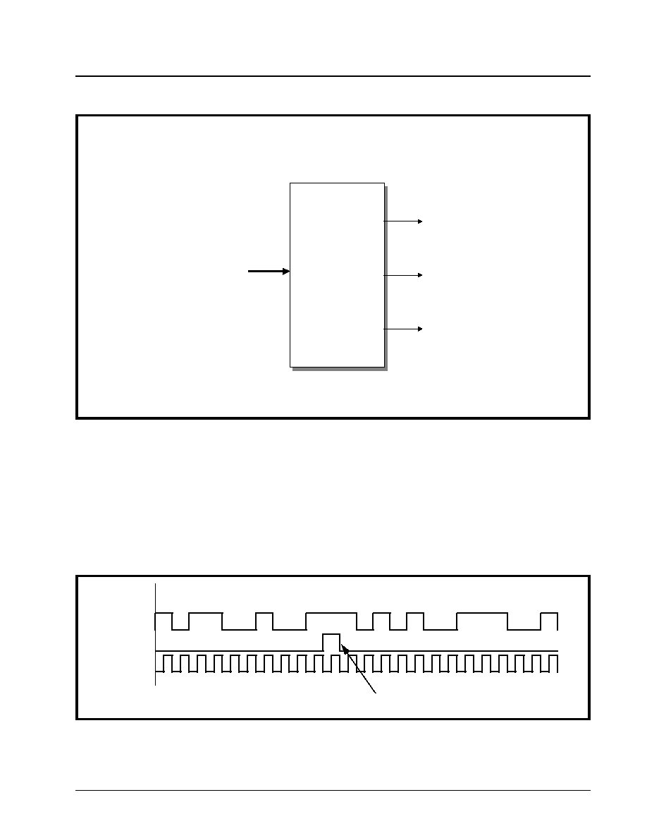
·Á
·Á
·Á
·Á
DS3/E3 FRAMER IC
XRT7250
REV. 1.1.1
175
The Transmit DS3 LIU Interface block can transmit
data to the LIU IC or other external circuitry via two
different output modes: Unipolar or Bipolar. If the Un-
ipolar (or Single Rail) mode is selected, then the con-
tents of the DS3 Frame is output, in a binary (NRZ
manner) data stream via the TxPOS pin to the LIU IC.
The TxNEG pin will only be used to denote the frame
boundaries. TxNEG will pulse "High" for one bit peri-
od, at the start of each new DS3 frame, and will re-
main "Low" for the remainder of the frame. Figure 67
presents an illustration of the TxPOS and TxNEG sig-
nals during data transmission while the Transmit DS3
LIU Interface block is operating in the Unipolar mode.
This mode is sometimes referred to as Single Rail
mode because the data pulses only exist in one po-
larity: positive.
When the Transmit DS3 LIU Interface block is operat-
ing in the Bipolar (or Dual Rail) mode, then the con-
tents of the DS3 Frame is output via both the TxPOS
and TxNEG pins. If the Bipolar mode is chosen, then
the DS3 data to the LIU can be transmitted via one of
two different line codes: Alternate Mark Inversion
(AMI) or Binary - 3 Zero Substitution (B3ZS). Each
one of these line codes will be discussed below. Bi-
F
IGURE
66. A S
IMPLE
I
LLUSTRATION
OF
THE
T
RANSMIT
DS3 LIU I
NTERFACE
BLOCK
From Transmit DS3
Framer Block
TxPOS
TxNEG
TxLineClk
Transmit DS3
LIU Interface
Block
F
IGURE
67. T
HE
B
EHAVIOR
OF
T
X
POS
AND
T
X
NEG
SIGNALS
DURING
DATA
TRANSMISSION
WHILE
THE
T
RANSMIT
DS3 LIU I
NTERFACE
IS
OPERATING
IN
THE
U
NIPOLAR
M
ODE
TxPOS
TxNEG
TxLineClk
Data
1 0 1 1 0 0 1 0 0 1 1 1 0 1 0 1 0 0 1 1 1 0 0 1
Frame Boundary

XRT7250
DS3/E3 FRAMER IC
·Á
·Á
·Á
·Á
REV. 1.1.1
176
polar mode is sometimes referred to as Dual Rail be-
cause the data pulses occur in two polarities: positive
and negative. The role of the TxPOS, TxNEG and
TxLineClk output pins, for this mode are discussed
below.
TxPOS - Transmit Positive Polarity Pulse: The
Transmit DS3 LIU Interface block will assert this out-
put to the LIU IC when it desires for the LIU to gener-
ate and transmit a positive polarity pulse to the re-
mote terminal equipment.
TxNEG - Transmit Negative Polarity Pulse: The
Transmit DS3 LIU Interface block will assert this out-
put to the LIU IC when it desires for the LIU to gener-
ate and transmit a negative polarity pulse to the re-
mote terminal equipment.
TxLineClk - Transmit Line Clock: The LIU IC uses
this signal from the Transmit DS3 LIU Interface block
to sample the state of its TxPOS and TxNEG inputs.
The results of this sampling dictates the type of pulse
(positive polarity, zero, or negative polarity) that it will
generate and transmit to the remote Receive DS3
Framer.
4.2.5.1
Selecting the various Line Codes
Either the Unipolar Mode or Bipolar Mode can be se-
lected by writing the appropriate value to Bit 3 of the I/
O Control Register (Address = 0x01), as shown be-
low.
Table 32 relates the value of this bit field to the Trans-
mit DS3 LIU Interface Output Mode.
N
OTES
:
1. The default condition is the Bipolar Mode.
2. This selection also effects the operation of the
Receive DS3 LIU Interface block
4.2.5.1.1
The Bipolar Mode Line Codes
If framer is to be operated in the Bipolar Mode, then
the DS3 data-stream can be transmitted via the AMI
(Alternate Mark Inversion) or the B3ZS Line Codes.
The definition of AMI and B3ZS line codes follow.
4.2.5.1.1.1
The AMI Line Code
AMI or Alternate Mark Inversion, means that consec-
utive one's pulses (or marks) will be of opposite polar-
ity with respect to each other. The line code involves
the use of three different amplitude levels: +1, 0, and -
1. +1 and -1 amplitude signals are used to represent
one's (or mark) pulses and the "0" amplitude pulses
(or the absence of a pulse) are used to represent ze-
ros (or space) pulses. The general rule for AMI is: if a
given mark pulse is of positive polarity, then the very
next mark pulse will be of negative polarity and vice
versa. This alternating-polarity relationship exists be-
tween two consecutive mark pulses, independent of
the number of 'zeros' that may exist between these
two pulses. Figure 68 presents an illustration of the
AMI Line Code as would appear at the TxPOS and
TxNEG pins of the Framer, as well as the output sig-
nal on the line.
I/O CONTROL REGISTER (ADDRESS = 0X01)
B
IT
7
B
IT
6
B
IT
5
B
IT
4
B
IT
3
B
IT
2
B
IT
1
B
IT
0
Disable TxLOC
LOC
Disable
RxLOC
AMI/ZeroSup*
Unipolar/
Bipolar*
TxLine CLK
Invert
RxLine CLK
Invert
Reframe
R/W
RO
R/W
R/W
R/W
R/W
R/W
R/W
1
0
1
0
0
0
0
0
T
ABLE
32: T
HE
R
ELATIONSHIP
BETWEEN
THE
CONTENT
OF
B
IT
3 (U
NIPOLAR
/B
IPOLAR
*)
WITHIN
THE
UNI I/O
C
ONTROL
R
EGISTER
AND
THE
T
RANSMIT
DS3 F
RAMER
L
INE
I
NTERFACE
O
UTPUT
M
ODE
B
IT
3
T
RANSMIT
DS3 F
RAMER
LIU I
NTERFACE
O
UTPUT
M
ODE
0
Bipolar Mode: AMI or B3ZS Line Codes are Transmitted and Received
1
Unipolar (Single Rail) Mode of transmission and reception of DS3 data is selected.
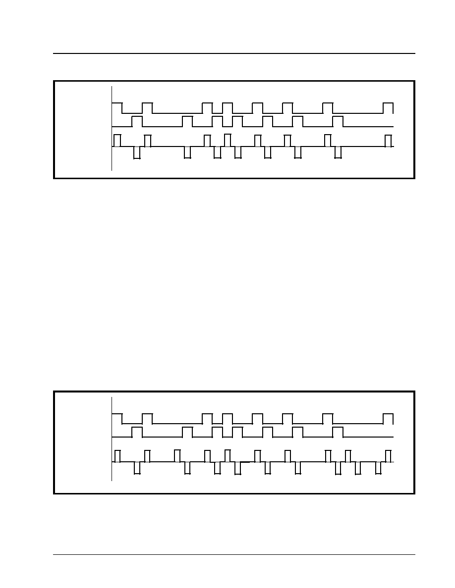
·Á
·Á
·Á
·Á
DS3/E3 FRAMER IC
XRT7250
REV. 1.1.1
177
N
OTE
: One of the main reasons that the AMI Line Code
has been chosen for driving transformer-coupled media is
that this line code introduces no dc component, thereby
minimizing dc distortion in the line.
4.2.5.1.1.2
The B3ZS Line Code
The Transmit DS3 Framer and the associated LIU IC
combine the data and timing information (originating
from the TxLineClk signal) into the line signal that is
transmitted to the far-end receiver. The far-end re-
ceiver has the task of recovering this data and timing
information from the incoming DS3 data stream.
Many clock and data recovery schemes rely on the
use of Phase Locked Loop technology. Phase-
Locked-Loop (PLL) technology for clock recovery re-
lies on transitions in the line signal, in order to main-
tain lock with the incoming DS3 data stream. Howev-
er, PLL-based clock recovery scheme, are vulnerable
to the occurrence of a long stream of consecutive ze-
ros (e.g., the absence of transitions). This scenario
can cause the PLL to lose lock with the incoming DS3
data, thereby causing the clock and data recovery
process of the receiver to fail. Therefore, some ap-
proach is needed to insure that such a long string of
consecutive zeros can never happen. One such tech-
nique is B3ZS encoding. B3ZS (or Bipolar 3 Zero
Substitution) is a form of AMI line coding that imple-
ments the following rule.
In general the B3ZS line code behaves just like AMI
with the exception of the case when a long string of
consecutive zeros occur on the line. Any string of 3
consecutive zeros will be replaced with either a 00V
or a B0V where B refers to a Bipolar pulse (e.g., a
pulse with a polarity that is compliant with the AMI
coding rule). And V refers to a Bipolar Violation pulse
(e.g., a pulse with a polarity that violates the alternat-
ing polarity scheme of AMI.) The decision between
inserting an 00V or a B0V is made to insure that an
odd number of Bipolar (B) pulses exist between any
two Bipolar Violation (V) pulses. Figure 69 presents a
timing diagram that illustrates examples of B3ZS en-
coding.
The user chooses between AMI or B3ZS line coding
by writing to bit 4 of the I/O Control Register (Address
= 0x01), as shown below.
F
IGURE
68. I
LLUSTRATION
OF
AMI L
INE
C
ODE
Data
TxPOS
TxNEG
Line Signal
1 0 1 1 0 0 0 1 0 1 1 1 1 0 1 1 0 1 1 0 0 1 1 0 0 0 0 1
F
IGURE
69. I
LLUSTRATION
OF
TWO
EXAMPLES
OF
B3ZS E
NCODING
Data
TxPOS
TxNEG
1 0 1 1 0 0 0 1 0 1 1 1 1 0 1 1 0 1 1 0 0 1 1 1 0 0 0 1
0 0 V
Line Signal
B 0 V
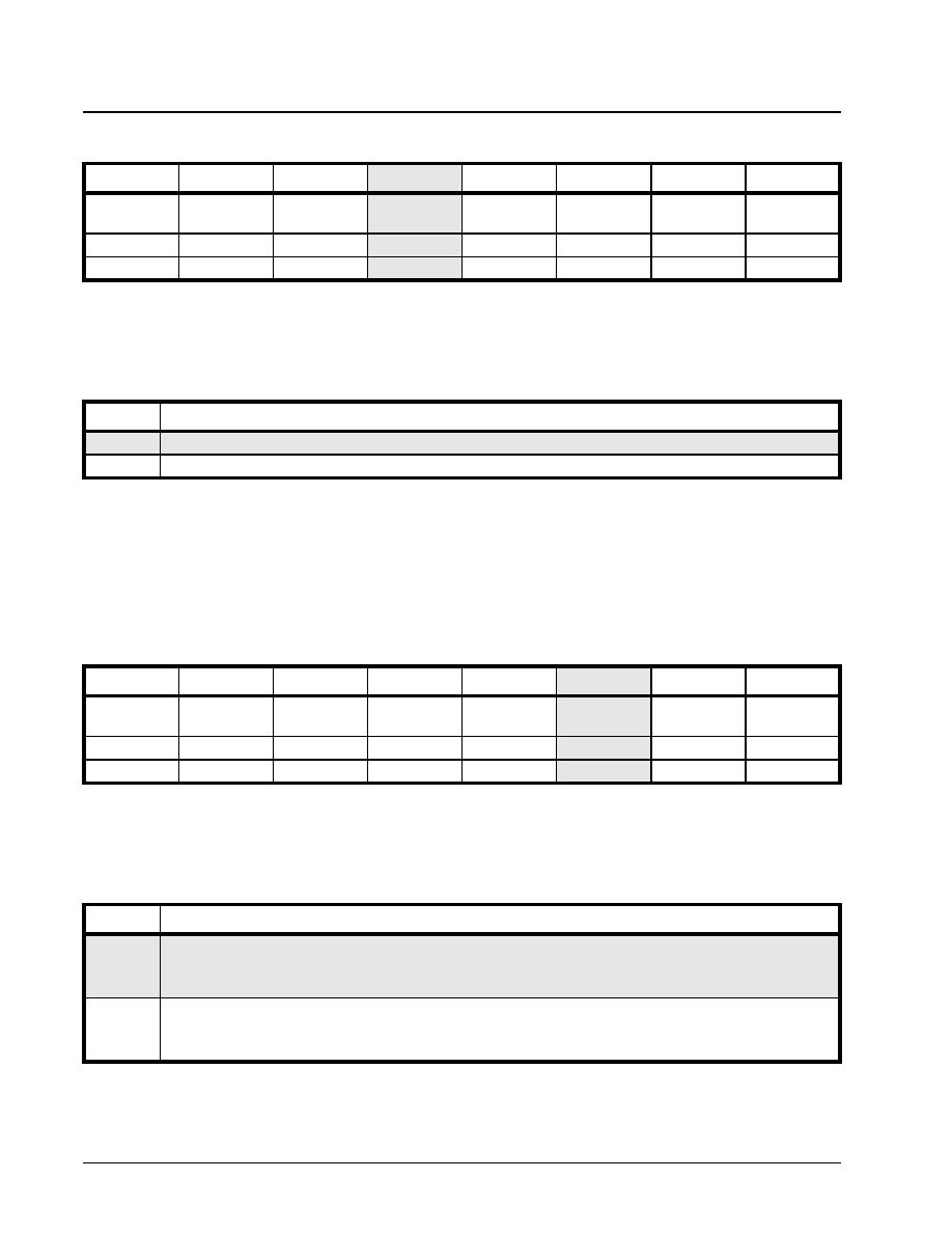
XRT7250
DS3/E3 FRAMER IC
·Á
·Á
·Á
·Á
REV. 1.1.1
178
Table 33 relates the content of this bit-field to the Bi-
polar Line Code that DS3 Data will be transmitted and
received at.
N
OTES
:
1. This bit is ignored if the Unipolar mode is selected.
2. This selection also effects the operation of the
Receive DS3 LIU Interface block
4.2.5.2
TxLineClk Clock Edge Selection
The Framer also allows the user to specify whether
the DS3 output data (via TxPOS and/or TxNEG out-
put pins) is to be updated on the rising or falling edg-
es of the TxLineClk signal. The purpose of this fea-
ture is to insure that the Framer will always be able to
output data to the LIU IC, in such a way that the LIU
set-up and hold time requirements can always be
met. This selection is made by writing to bit 2 of the I/
O Control Register, as depicted below.
Table 34 relates the contents of this bit field to the
clock edge of TxClk that DS3 Data is output on the
TxPOS and/or TxNEG output pins.
N
OTE
: The user will typically make the selection based
upon the set-up and hold time requirements of the Transmit
LIU IC.
I/O CONTROL REGISTER (ADDRESS = 0X01)
B
IT
7
B
IT
6
B
IT
5
B
IT
4
B
IT
3
B
IT
2
B
IT
1
B
IT
0
Disable TxLOC
LOC
Disable
RxLOC
AMI/ZeroSup*
Unipolar/
Bipolar*
TxLine CLK
Invert
RxLine CLK
Invert
Reframe
R/W
RO
R/W
R/W
R/W
R/W
R/W
R/W
1
0
1
0
0
0
0
0
T
ABLE
33: T
HE
R
ELATIONSHIP
BETWEEN
B
IT
4 (AMI/B3ZS*)
WITHIN
THE
I/O C
ONTROL
R
EGISTER
AND
THE
B
IPOLAR
L
INE
C
ODE
THAT
IS
OUTPUT
BY
THE
T
RANSMIT
DS3 LIU I
NTERFACE
B
LOCK
B
IT
4
B
IPOLAR
L
INE
C
ODE
0
B3ZS
1
AMI
II/O CONTROL REGISTER (ADDRESS = 0X01)
B
IT
7
B
IT
6
B
IT
5
B
IT
4
B
IT
3
B
IT
2
B
IT
1
B
IT
0
Disable TxLOC
LOC
Disable
RxLOC
AMI/ZeroSup*
Unipolar/
Bipolar*
TxLine CLK
Invert
RxLine CLK
Invert
Reframe
R/W
RO
R/W
R/W
R/W
R/W
R/W
R/W
1
0
1
0
0
X
X
0
T
ABLE
34: T
HE
R
ELATIONSHIP
BETWEEN
THE
CONTENTS
OF
B
IT
2 (T
X
L
INE
C
LK
I
NV
)
WITHIN
THE
I/O C
ONTROL
R
EGISTER
AND
THE
T
X
L
INE
C
LK
CLOCK
EDGE
THAT
T
X
POS
AND
T
X
NEG
ARE
UPDATED
ON
B
IT
2
R
ESULT
0
Rising Edge:
Outputs on TxPOS and/or TxNEG are updated on the rising edge of TxLineClk.
See Figure 70 for timing relationship between TxLineClk, TxPOS and TxNEG signals, for this selection.
1
Falling Edge:
Outputs on TxPOS and/or TxNEG are updated on the falling edge of TxLineClk.
See Figure 71 for timing relationship between TxLineClk, TxPOS and TxNEG signals, for this selection.
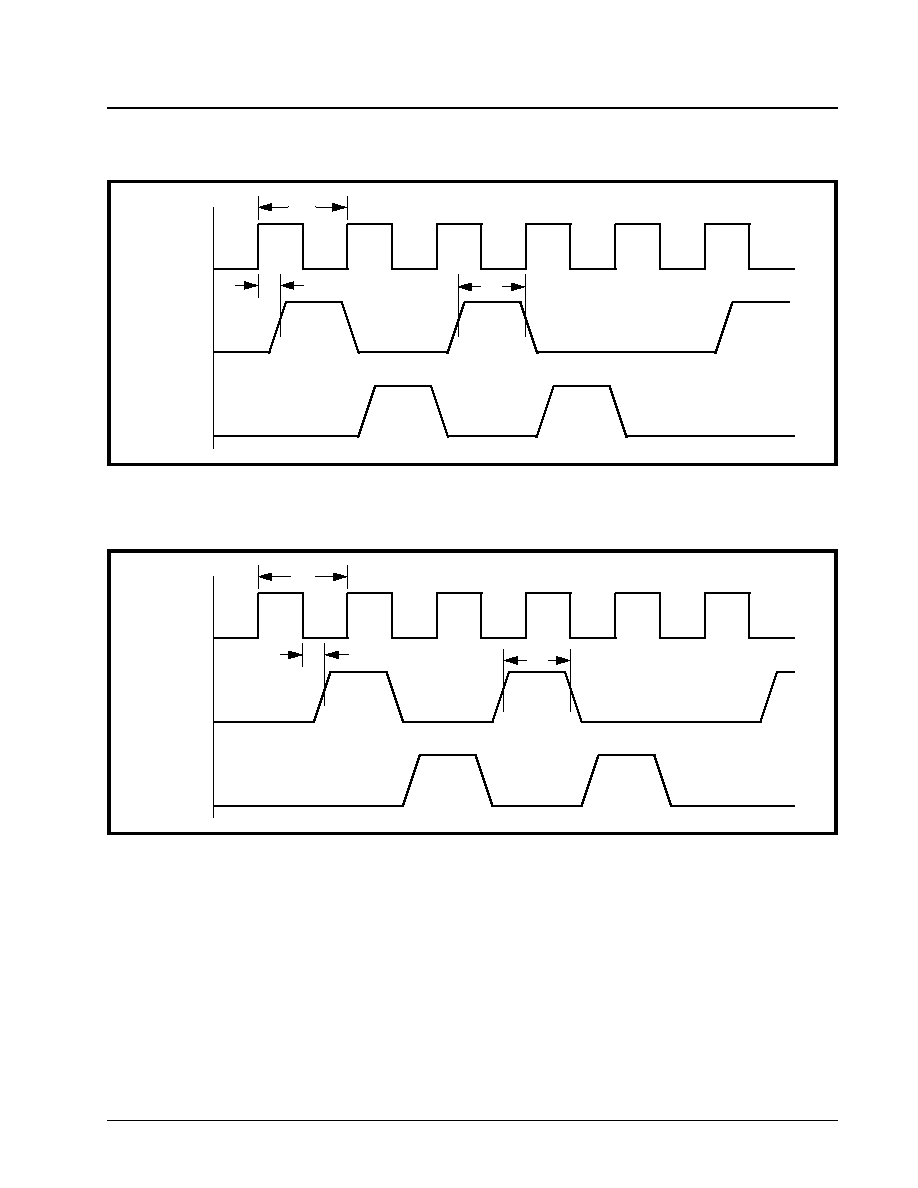
·Á
·Á
·Á
·Á
DS3/E3 FRAMER IC
XRT7250
REV. 1.1.1
179
4.2.6
Transmit Section Interrupt Processing
The Transmit Section of the XRT7250 can generate
an interrupt to the Microcontroller/Microprocessor for
the following two reasons.
∑ Completion of Transmission of FEAC Message
∑ Completion of Transmission of LAPD Message
4.2.6.1
Enabling Transmit Section Interrupts
As mentioned in Section 1.6, the Interrupt Structure,
within the XRT7250 contains two hierarchical levels:
∑ Block Level
∑ Source Level
The Block Level
The Enable State of the Block Level for the Transmit
Section Interrupts dictates whether or not interrupts
(if enabled at the source level), are actually enabled.
The user can enable or disable these Transmit Sec-
tion interrupts, at the Block Level by writing the appro-
priate data into Bit 1 (Tx DS3/E3 Interrupt Enable)
within the Block Interrupt Enable register (Address =
0x04), as illustrated below.
F
IGURE
70. W
AVEFORM
/T
IMING
R
ELATIONSHIP
BETWEEN
T
X
L
INE
C
LK
, T
X
POS
AND
T
X
NEG - T
X
POS
AND
T
X
NEG
ARE
CONFIGURED
TO
BE
UPDATED
ON
THE
RISING
EDGE
OF
T
X
L
INE
C
LK
TxLineClk
TxPOS
TxNEG
t32
t30
t33
F
IGURE
71. W
AVEFORM
/T
IMING
R
ELATIONSHIP
BETWEEN
T
X
L
INE
C
LK
, T
X
POS
AND
T
X
NEG - T
X
POS
AND
T
X
NEG
ARE
CONFIGURED
TO
BE
UPDATED
ON
THE
FALLING
EDGE
OF
T
X
L
INE
C
LK
TxLineClk
TxPOS
TxNEG
t31
t32
t33

XRT7250
DS3/E3 FRAMER IC
·Á
·Á
·Á
·Á
REV. 1.1.1
180
Setting this bit-field to "1" enables the Transmit Sec-
tion (at the Block Level) for Interrupt Generation.
Conversely, setting this bit-field to "0" disables the
Transmit Section for interrupt generation.
What does it mean for the Transmit Section Inter-
rupts to be enabled or disabled at the Block Lev-
el?
If the Transmit Section is disabled (for interrupt gener-
ation) at the Block Level, then ALL Transmit Section
interrupts are disabled, independent of the interrupt
enable/disable state of the source level interrupts.
If the Transmit Section is enabled (for interrupt gener-
ation) at the block level, then a given interrupt will be
enabled at the source level. Conversely, if the Trans-
mit Section is enabled (for interrupt generation) at the
Block level, then a given interrupt will still be disabled,
if it is disabled at the source level.
As mentioned earlier, the Transmit Section of the
XRT7250 Framer IC contains the following two inter-
rupts
∑ Completion of Transmission of FEAC Message
Interrupt.
∑ Completion of Transmission of LAPD Message
Interrupt.
The Enabling/Disabling and Servicing of each of
these interrupts is described below.
4.2.6.1.1
The Completion of Transmission of
FEAC Message Interrupt.
If the Transmit Section interrupts have been enabled
at the Block level, then the user can enable or disable
the Completion of Transmission of a FEAC Message
Interrupt by writing the appropriate value into Bit 4 (Tx
FEAC Interrupt Enable) within the Transmit DS3
FEAC Configuration & Status Register (Address =
0x31) as illustrated below.
Setting this bit-field to "1" enables the Completion of
Transmission of a FEAC Message Interrupt. Con-
versely, setting this bit-field to "0" disables this inter-
rupt.
4.2.6.1.2
Servicing the Completion of Trans-
mission of a FEAC Message Interrupt
As mentioned earlier, once the user commands the
Transmit FEAC Processor to begin its transmission of
a FEAC Message, it will do the following.
1. It will read in the six-bit contents of the Tx DS3
FEAC Register (Address = 0x32) and encapsu-
late these 6 bits into a 16-bit data structure.
2. The Transmit FEAC Processor will then begin to
transmit this 16-bit data structure (to the Remote
Terminal Equipment) repeatedly for 10 consecu-
tive times.
3. Upon completion of the 10th transmission, the
XRT7250 Framer IC will generate the Completion
of Transmission of a FEAC Message Interrupt to
the Microcontroller/Microprocessor. Once the
XRT7250 Framer IC generates this interrupt, it
will do the following.
∑ Assert the Interrupt Output pin (INT) by toggling it
"Low".
BLOCK INTERRUPT ENABLE REGISTER (ADDRESS = 0X04)
B
IT
7
B
IT
6
B
IT
5
B
IT
4
B
IT
3
B
IT
2
B
IT
1
B
IT
0
RxDS3/E3
Interrupt
Enable
Not Used
TxDS3/E3
Interrupt
Enable
One Second
Interrupt
Enable
R/W
RO
RO
RO
RO
RO
R/W
R/W
0
0
0
0
0
0
0
0
TRANSMIT DS3 FEAC CONFIGURATION & STATUS REGISTER (ADDRESS = 0X31)
B
IT
7
B
IT
6
B
IT
5
B
IT
4
B
IT
3
B
IT
2
B
IT
1
B
IT
0
Not Used
Tx FEAC
Interrupt
Enable
TxFEAC
Interrupt
Status
TxFEAC
Enable
TxFEAC
GO
TxFEAC
Busy
RO
RO
RO
R/W
RUR
R/W
R/W
RO
0
0
0
X
0
0
0
0

·Á
·Á
·Á
·Á
DS3/E3 FRAMER IC
XRT7250
REV. 1.1.1
181
∑ Set Bit 3 (Tx FEAC Interrupt Status) within the Tx
DS3 FEAC Configuration & Status Register, as
illustrated below.
The purpose of this interrupt is to alert the Microcon-
troller/Microprocessor that the Transmit FEAC Pro-
cessor has completed its transmission of a given
FEAC message and is now ready to transmit the next
FEAC Message, to the Remote Terminal Equipment.
4.2.6.1.3
The Completion of Transmission of
the LAPD Message Interrupt
If the Transmit Section interrupts have been enabled
at the Block level, then the user can enable or disable
the Completion of Transmission of a LAPD Message
Interrupt by writing the appropriate value into Bit 1
(TxLAPD Interrupt Enable) within the Tx DS3 LAPD
Status & Interrupt Register (Address = 0x34), as illus-
trated below.
Setting this bit-field to "1' enables the Completion of
Transmission of a LAPD Message Interrupt. Con-
versely, setting this bit-field to "0" disables the Com-
pletion of Transmission of a LAPD Message interrupt.
4.2.6.1.4
Servicing the Completion of Trans-
mission of a LAPD Message Interrupt
As mentioned previously, once the user commands
the LAPD Transmitter to begin its transmission of a
LAPD Message, it will do the following.
1. It will parse through the contents of the Transmit
LAPD Message Buffer (located at address loca-
tions 0x86 through 0xDD) and search for a string
of five (5) consecutive "1's". If the LAPD Trans-
mitter finds a string of five consecutive "1's"
(within the content of the LAPD Message Buffer,
then it will insert a "0" immediately after this
string.
2. It will compute the FCS (Frame Check Sequence)
value and append this value to the back-end of
the user-message.
3. It will read out of the content of the user (zero-
stuffed) message and will encapsulate this data
into a LAPD Message frame.
4. Finally, it will begin transmitting the contents of
this LAPD Message frame via the "DL" bits, within
each outbound DS3 frame.
5. Once the LAPD Transmitter has completed its
transmission of this LAPD Message frame (to the
Remote Terminal Equipment), the XRT7250
Framer IC will generate the Completion of Trans-
mission of a LAPD Message Interrupt to the
Microcontroller/Microprocessor. Once the
XRT7250 Framer IC generates this interrupt, it
will do the following.
∑ Assert the Interrupt Output pin (INT) by toggling it
"Low".
∑ Set Bit 0 (TxLAPD Interrupt Status) within the
TxDS3 LAPD Status and Interrupt Register, as
illustrated below.
TRANSMIT DS3 FEAC CONFIGURATION & STATUS REGISTER (ADDRESS = 0X31)
B
IT
7
B
IT
6
B
IT
5
B
IT
4
B
IT
3
B
IT
2
B
IT
1
B
IT
0
Not Used
Tx FEAC
Interrupt
Enable
TxFEAC
Interrupt
Status
TxFEAC
Enable
TxFEAC
GO
TxFEAC
Busy
RO
RO
RO
R/W
RUR
R/W
R/W
RO
0
0
0
1
1
0
0
0
TXDS3 LAPD STATUS AND INTERRUPT REGISTER (ADDRESS = 0X34)
B
IT
7
B
IT
6
B
IT
5
B
IT
4
B
IT
3
B
IT
2
B
IT
1
B
IT
0
Not Used
TxDL Start
TxDL Busy
TxLAPD
Interrupt
Enable
TxLAPD
Interrupt
Status
RO
RO
RO
RO
R/W
RO
R/W
RUR
0
0
0
0
0
0
0
0

XRT7250
DS3/E3 FRAMER IC
·Á
·Á
·Á
·Á
REV. 1.1.1
182
The purpose of this interrupt is to alert the Microcon-
troller/MIcroprocessor that the LAPD Transmitter has
completed its transmission of a given LAPD (or PM-
DL) Message, and is now ready to transmit the next
PMDL Message, to the Remote Terminal Equipment.
4.3
T
HE
R
ECEIVE
S
ECTION
OF
THE
XRT7250 (DS3
M
ODE
O
PERATION
)
When the XRT7250 has been configured to operate
in the DS3 Mode, the Receive Section of the
XRT7250 consists of the following functional blocks.
∑ Receive LIU Interface block
∑ Receive HDLC Controller block
∑ Receive DS3 Framer block
∑ Receive Overhead Data Output Interface block
∑ Receive Payload Data Output Interface block
Figure 72 presents a simple illustration of the Receive
Section of the XRT7250 Framer IC.
Each of these functional blocks will be discussed in
detail in this document.
4.3.1
The Receive DS3 LIU Interface Block
The purpose of the Receive DS3 LIU Interface block
is two-fold:
TXDS3 LAPD STATUS AND INTERRUPT REGISTER (ADDRESS = 0X34)
B
IT
7
B
IT
6
B
IT
5
B
IT
4
B
IT
3
B
IT
2
B
IT
1
B
IT
0
Not Used
TxDL Start
TxDL Busy
TxLAPD
Interrupt
Enable
TxLAPD
Interrupt
Status
RO
RO
RO
RO
R/W
RO
R/W
RUR
0
0
0
0
0
0
0
1
F
IGURE
72. A S
IMPLE
I
LLUSTRATION
OF
THE
R
ECEIVE
S
ECTION
OF
THE
XRT7250,
WHEN
IT
HAS
BEEN
CONFIGURED
TO
OPERATE
IN
THE
DS3 M
ODE
Receive Payload
Data Input
Interface Block
Receive DS3/E3
Framer Block
Receive LIU
Interface
Block
RxSer
RxNib[3:0]
RxClk
RxPOS
RxNEG
RxLineClk
Receive Overhead
Input
Interface Block
RxOHClk
RxOHInd
RxOH
RxOHEnable
RxOHFrame
RxFrame
Rx DS3 HDLC
Controller/Buffer
Rx DS3 HDLC
Controller/Buffer
From Microprocessor
Interface Block
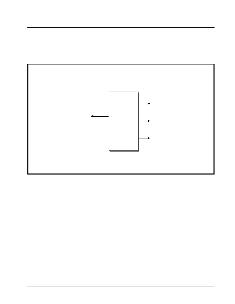
·Á
·Á
·Á
·Á
DS3/E3 FRAMER IC
XRT7250
REV. 1.1.1
183
1. To receive encoded digital data from the DS3 LIU
IC.
2. To decode this data, convert it into a binary data
stream and to route this data to the Receive DS3
Framer block.
Figure 73 presents a simple illustration of the Receive
DS3 LIU Interface block.
The Receive Section of the XRT7250 will via the Re-
ceive DS3 LIU Interface Block receive timing and data
information from the incoming DS3 data stream. The
DS3 Timing information will be received via the RxLi-
neClk input pin and the DS3 data information will be
received via the RxPOS and RxNEG input pins. The
Receive DS3 LIU Interface block is capable of receiv-
ing DS3 data pulses in unipolar or bipolar format. If
the Receive DS3 framer is operating in the bipolar for-
mat, then it can be configured to decode either AMI or
B3ZS line code data. Each of these input formats
and line codes will be discussed in detail, below.
4.3.1.1
Unipolar Decoding
If the Receive DS3 LIU Interface block is operating in
the Unipolar (single-rail) mode, then it will receive the
Single Rail NRZ DS3 data pulses via the RxPOS in-
put pin. The Receive DS3 LIU Interface block will al-
so receive its timing signal via the RxLineClk signal.
N
OTE
: The RxLineClk signal will function as the timing
source for the entire Receive Section of the XRT7250.
No data pulses will be applied to the RxNEG input
pin. The Receive DS3 LIU Interface block receives a
logic "1" when a logic "1" level signal is present at the
RxPOS pin, during the sampling edge of the RxLi-
neClk signal. Likewise, a logic "0" is received when a
logic "0" level signal is applied to the RxPOS pin.
Figure 74 presents an illustration of the behavior of
the RxPOS, RxNEG and RxLineClk input pins when
the Receive DS3 LIU Interface block is operating in
the Unipolar mode.
F
IGURE
73. A S
IMPLE
I
LLUSTRATION
OF
THE
R
ECEIVE
DS3 LIU I
NTERFACE
B
LOCK
RxPOS
RxNEG
RxLineClk
To Receive DS3
Framer Block
Receive DS3
LIU Interface
Block
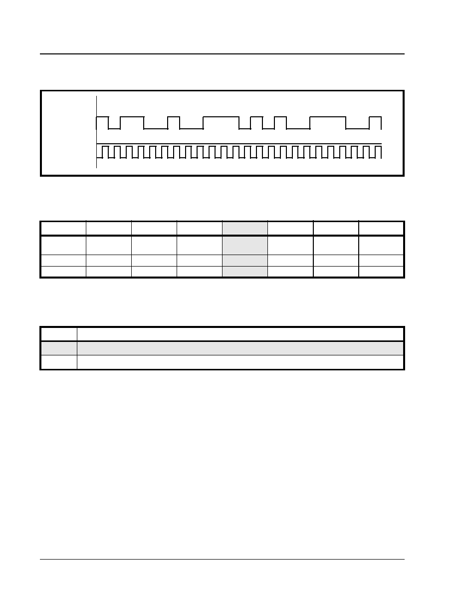
XRT7250
DS3/E3 FRAMER IC
·Á
·Á
·Á
·Á
REV. 1.1.1
184
The user can configure the Receive DS3 LIU Inter-
face block to operate in either the Unipolar or the Bi-
polar Mode by writing the appropriate data to the I/O
Control Register, as depicted below.
Table 35 relates the value of this bit-field to the Re-
ceive DS3 LIU Interface Input Mode.
N
OTES
:
1. The default condition is the Bipolar Mode.
2. This selection also effects the Transmit DS3 Framer
Line Interface Output Mode
4.3.1.2
Bipolar Decoding
If the Receive DS3 LIU Interface block is operating in
the Bipolar Mode, then it will receive the DS3 data
pulses via both the RxPOS, RxNEG, and the RxLi-
neClk input pins. Figure 75 presents a circuit dia-
gram illustrating how the Receive DS3 LIU Interface
block interfaces to the Line Interface Unit while the
Framer is operating in Bipolar mode. The Receive
DS3 LIU Interface block can be configured to decode
the incoming data from either the AMI or B3ZS line
codes.
F
IGURE
74. B
EHAVIOR
OF
THE
R
X
POS, R
X
NEG
AND
R
X
L
INE
C
LK
SIGNALS
DURING
DATA
RECEPTION
OF
U
NIPOLAR
D
ATA
RxPOS
RxNEG
RxLineClk
Data
1 0 1 1 0 0 1 0 0 1 1 1 0 1 0 1 0 0 1 1 1 0 0 1
II/O CONTROL REGISTER (ADDRESS = 0X01)
B
IT
7
B
IT
6
B
IT
5
B
IT
4
B
IT
3
B
IT
2
B
IT
1
B
IT
0
Disable TxLOC
LOC
Disable
RxLOC
AMI/ZeroSup*
Unipolar/
Bipolar*
TxLine CLK
Invert
RxLine CLK
Invert
Reframe
R/W
RO
R/W
R/W
R/W
R/W
R/W
R/W
1
0
1
0
0
0
0
0
T
ABLE
35: T
HE
R
ELATIONSHIP
BETWEEN
THE
CONTENTS
OF
B
IT
2 (T
X
L
INE
C
LK
I
NV
)
WITHIN
THE
I/O C
ONTROL
R
EGISTER
AND
THE
T
X
L
INE
C
LK
CLOCK
EDGE
THAT
T
X
POS
AND
T
X
NEG
ARE
UPDATED
ON
B
IT
3
R
ECEIVE
DS3 LIU I
NTERFACE
I
NPUT
M
ODE
0
.Bipolar Mode (Dual Rail): AMI or B3ZS Line Codes are Transmitted and Received.
1
Unipolar Mode (Single Rail) Mode of transmission and reception of DS3 data is selected.
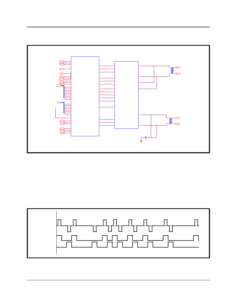
·Á
·Á
·Á
·Á
DS3/E3 FRAMER IC
XRT7250
REV. 1.1.1
185
4.3.1.2.1
AMI Decoding
AMI or Alternate Mark Inversion, means that consec-
utive one's pulses (or marks) will be of opposite polar-
ity with respect to each other. This line code involves
the use of three different amplitude levels: +1, 0, and -
1. The +1 and -1 amplitude signals are used to repre-
sent one's (or mark) pulses and the "0" amplitude
pulses (or the absence of a pulse) are used to repre-
sent zeros (or space) pulses. The general rule for the
AMI line code is: if a given mark pulse is of positive
polarity, then the very next mark pulse will be of nega-
tive polarity and vice versa. This alternating-polarity
relationship exists between two consecutive mark
pulses, independent of the number of zeros that exist
between these two pulses. Figure 76 presents an il-
lustration of the AMI Line Code as would appear at
the RxPOS and RxNEG input pins of the Framer, as
well as the corresponding output signal on the line.
N
OTE
: One of the reasons that the AMI Line Code has
been chosen for driving copper medium, isolated via trans-
formers, is that this line code has no dc component, thereby
eliminating dc distortion in the line.
4.3.1.2.2
B3ZS Decoding
F
IGURE
75. I
LLUSTRATION
ON
HOW
THE
R
ECEIVE
DS3 F
RAMER
(
WITHIN
THE
XRT7250 F
RAMER
IC)
BEING
INTER
-
FACE
TO
THE
XRT7300 L
INE
I
NTERFACE
U
NIT
,
WHILE
THE
F
RAMER
IS
OPERATING
IN
B
IPOLAR
M
ODE
5V
U1
XRT7250
TxPOS
65
TxNEG
64
TxLineClk
63
D M O
79
ExtLOS
78
RLOL
77
LLOOP
69
RLOOP
70
TAOS
68
TxLEV
67
ENCODIS
66
REQB
71
RxPOS
76
RxNEG
75
RxLineClk
74
MOTO
27
RESETB
28
A0
15
A1
16
A2
17
A3
18
A4
19
A5
20
A6
21
A7
22
A8
23
D0
32
D1
33
D2
34
D3
35
D4
36
D5
37
D6
38
D7
39
Rdy_Dtck
6
W R B _ R W
7
RDB_DS
10
CSB
8
ALE_AS
9
INTB
13
TxSER
46
TxInClk
43
TxFrame
61
RxSer
86
RxClk
88
RxFrame
90
RxLOS
95
RxOOF
94
RxRED
93
RxAIS
87
NIBBLEINTF
25
U2
XRT7300
TPDATA
37
TNDATA
38
TCLK
36
RCLK1
31
RNEG
32
RPOS
33
TTIP
41
TRING
40
MTIP
44
MRING
43
RRING
9
RTIP
8
D M O
4
RLOS
24
RLOL
23
LLB
14
RLB
15
TAOS
2
TxLEV
1
ENCODIS
21
REQDIS
12
T1
1:1
1
5
4
8
T2
1:1
1
5
4
8
R1
36
1
2
R2
36
1
2
R6
37.5
1
2
R3
270
1
2
R4
270
1
2
R5
37.5
1
2
C1
0.01uF
1
2
TxSER
TxInClk
NIBBLEINTF
RESETB
RTIP
RRING
CSB
R W
DS
AS
TxFrame
RxSer
RxClk
RxFrame
RxLOS
RxOOF
RxRED
RxAIS
A[8:0]
TRING
TTIP
INTB
D[7:0]
INTB
F
IGURE
76. I
LLUSTRATION
OF
AMI L
INE
C
ODE
Data 1 0 1 1 0 0 0 1 0 1 1 1 1 0 1 1 0 1 1 0 0 1 1 0 0 0 0 1
RxPOS
RxNEG
Line Signal
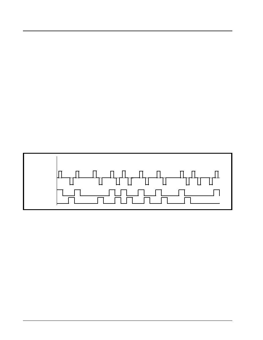
XRT7250
DS3/E3 FRAMER IC
·Á
·Á
·Á
·Á
REV. 1.1.1
186
The Transmit DS3 LIU Interface block and the associ-
ated LIU embed and combine the data and clocking
information into the line signal that is transmitted to
the remote terminal equipment. The remote terminal
equipment has the task of recovering this data and
timing information from the incoming DS3 data
stream. Most clock and data recovery schemes rely
on the use of Phase-Locked-Loop technology. One of
the problems of using Phase-Locked-Loop (PLL)
technology for clock recovery is that it relies on transi-
tions in the line signal, in order to maintain lock with
the incoming DS3 data-stream. Therefore, these
clock recovery scheme, are vulnerable to the occur-
rence of a long stream of consecutive zeros (e.g., no
transitions in the line). This scenario can cause the
PLL to lose lock with the incoming DS3 data, thereby
causing the clock and data recovery process of the
receiver to fail. Therefore, some approach is needed
to insure that such a long string of consecutive zeros
can never happen. One such technique is B3ZS (or
Bipolar 3 Zero Substitution) encoding.
In general the B3ZS line code behaves just like AMI
with the exception of the case when a long string of
consecutive zeros occurs on the line. Any 3 consecu-
tive zeros will be replaced with either a 00V or a B0V
where B refers to a Bipolar pulse (e.g., a pulse with a
polarity that is compliant with the alternating polarity
scheme of the AMI coding rule). And V refers to a Bi-
polar Violation pulse (e.g., a pulse with a polarity that
violates the alternating polarity scheme of AMI.) The
decision between inserting an 00V or a B0V is made
to insure that an odd number of Bipolar (B) pulses ex-
ist between any two Bipolar Violation (V) pulses. The
Receive DS3 Framer, when operating with the B3ZS
Line Code is responsible for decoding the B3ZS-en-
coded data back into a unipolar (binary-format). For
instance, if the Receive DS3 Framer detects a 00V or
a B0V pattern in the incoming pattern, the Receive
DS3 Framer will replace it with three consecutive ze-
ros. Figure 77 presents a timing diagram that illus-
trates examples of B3ZS decoding.
4.3.1.2.3
Line Code Violations
The Receive DS3 LIU Interface block will also check
the incoming DS3 data stream for line code viola-
tions. For example, when the Receive DS3 LIU Inter-
face block detects a valid bipolar violation (e.g., in
B3ZS line code), it will substitute three zeros into the
binary data stream. However, if the bipolar violation
is invalid, then an LCV (Line Code Violation) is
flagged and the PMON LCV Event Count Register
(Address = 0x50 and 0x51) will also be incremented.
Additionally, the LCV-One Second Accumulation Reg-
isters (Address = 0x6E and 0x6F) will be increment-
ed. For example: If the incoming DS3 data is B3ZS
encoded, the Receive DS3 LIU Interface block will al-
so increment the LCV One Second Accumulation
Register if three (or more) consecutive zeros are re-
ceived.
4.3.1.2.4
RxLineClk Clock Edge Selection
The incoming unipolar or bipolar data, applied to the
RxPOS and the RxNEG input pins are clocked into
the Receive DS3 LIU Interface block via the RxLi-
neClk signal. The Framer IC allows the user to spec-
ify which edge (e.g, rising or falling) of the RxLineClk
signal will sample and latch the signal at the RxPOS
and RxNEG input signals into the Framer IC. This
feature was included in the XRT7250 design in order
to insure that the user can always meet the RxPOS
and RxNEG to RxLineClk set-up and hold time re-
quirements. The user can make this selection by
writing the appropriate data to bit 1 of the I/O Control
Register, as depicted below.
F
IGURE
77. I
LLUSTRATION
OF
TWO
EXAMPLES
OF
B3ZS D
ECODING
Data 1 0 1 1 0 0 0 1 0 1 1 1 1 0 1 1 0 1 1 0 0 1 1 1 0 0 0 1
RxPOS
RxNEG
0 0 V
Line Signal
B 0 V
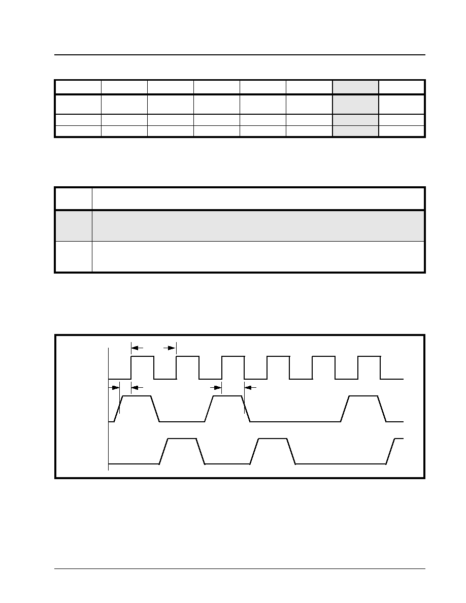
·Á
·Á
·Á
·Á
DS3/E3 FRAMER IC
XRT7250
REV. 1.1.1
187
Table 36 depicts the relationship between the value of
this bit-field to the sampling clock edge of RxLineClk.
Figure 78 and Figure 79 present the Waveform and
Timing Relationships between RxLineClk, RxPOS
and RxNEG for each of these configurations.
II/O CONTROL REGISTER (ADDRESS = 0X01)
B
IT
7
B
IT
6
B
IT
5
B
IT
4
B
IT
3
B
IT
2
B
IT
1
B
IT
0
Disable
TxLOC
LOC
Disable
RxLOC
AMI/ZeroSup*
Unipolar/
Bipolar*
TxLine CLK
Invert
RxLine CLK
Invert
Reframe
R/W
RO
R/W
R/W
R/W
R/W
R/W
R/W
1
0
1
0
0
0
0
0
T
ABLE
36: T
HE
R
ELATIONSHIP
BETWEEN
THE
CONTENTS
OF
B
IT
1 (R
X
L
INE
C
LK
I
NV
)
OF
THE
I/O C
ONTROL
R
EGISTER
,
AND
THE
SAMPLING
EDGE
OF
THE
R
X
L
INE
C
LK
SIGNAL
R
X
CLKI
NV
(B
IT
1)
R
ESULT
0
Rising Edge:
RxPOS and RxNEG are sampled at the rising edge of RxLineClk. See Figure 78 for timing relationship
between RxLineClk, RxPOS, and RxNEG.
1
Falling Edge:
RxPOS and RxNEG are sampled at the falling edge of RxLineClk. See Figure 79 for timing relationship
between RxLineClk, RxPOS, and RxNEG.
F
IGURE
78. W
AVEFORM
/T
IMING
R
ELATIONSHIP
BETWEEN
R
X
L
INE
C
LK
, R
X
POS
AND
R
X
NEG - W
HEN
R
X
POS
AND
R
X
NEG
ARE
TO
BE
SAMPLED
ON
THE
RISING
EDGE
OF
R
X
L
INE
C
LK
RxLineClk
RxPOS
RxNEG
t38
t39
t42
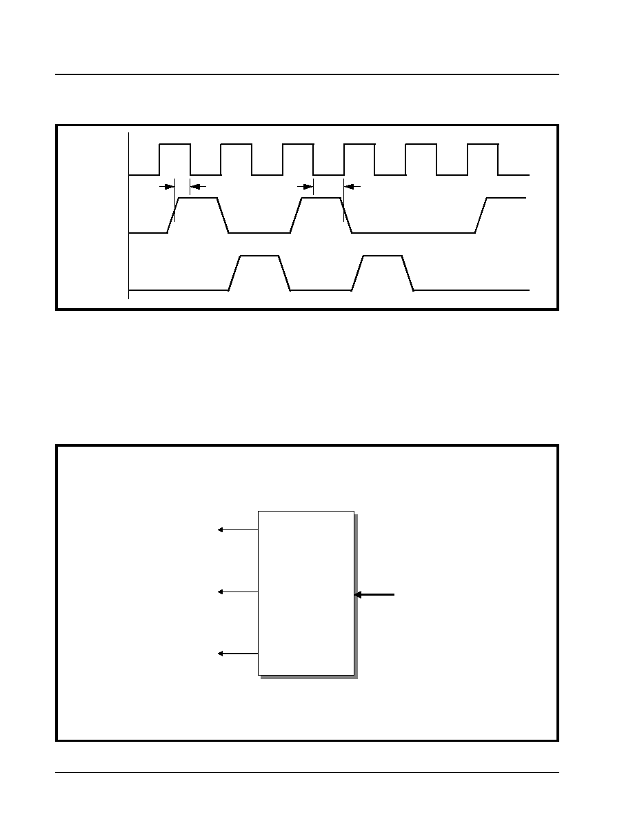
XRT7250
DS3/E3 FRAMER IC
·Á
·Á
·Á
·Á
REV. 1.1.1
188
4.3.2
The Receive DS3 Framer Block
The Receive DS3 Framer block accepts decoded
DS3 data from the Receive DS3 LIU Interface block,
and routes data to the following destinations.
∑ The Receive Payload Data Output Interface Block
∑ The Receive Overhead Data Output Interface
Block.
∑ The Receive DS3 HDLC Controller Block
Figure 80 presents a simple illustration of the Receive
DS3 Framer block along with the associated paths to
the other functional blocks within the Framer chip.
F
IGURE
79. W
AVEFORM
/T
IMING
R
ELATIONSHIP
BETWEEN
R
X
L
INE
C
LK
, R
X
POS
AND
R
X
NEG - W
HEN
R
X
POS
AND
R
X
NEG
ARE
TO
BE
SAMPLED
ON
THE
FALLING
EDGE
OF
R
X
L
INE
C
LK
RxLineClk
RxPOS
RxNEG
t40
t41
F
IGURE
80. A S
IMPLE
I
LLUSTRATION
OF
THE
R
ECEIVE
DS3 F
RAMER
B
LOCK
AND
THE
A
SSOCIATED
P
ATHS
TO
THE
O
THER
F
UNCTIONAL
B
LOCKS
Receive DS3 Framer
Block
Receive DS3 Framer
Block
To Receive DS3 HDLC
Buffer
Receive Overhead Data
Output Interface
Receive Payload Data
Output Interface
From Receive DS3
LIU Interface Block
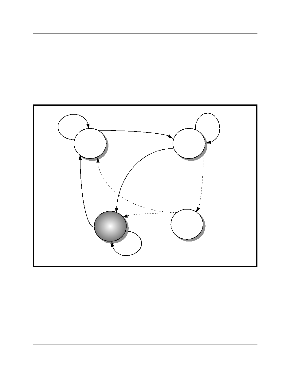
·Á
·Á
·Á
·Á
DS3/E3 FRAMER IC
XRT7250
REV. 1.1.1
189
Once the B3ZS (or AMI) encoded data has been de-
coded into a binary data-stream, the Receive DS3
Framer block will use portions of this data-stream in
order to synchronize itself to the remote terminal
equipment. At any given time, the Receive DS3
Framer block will be operating in one of two modes.
∑ The Frame Acquisition Mode: In this mode, the
Receive DS3 Framer block is trying to acquire syn-
chronization with the incoming DS3 frames, or
∑ The Frame Maintenance Mode: In this mode, the
Receive DS3 Framer block is trying to maintain
frame synchronization with the incoming DS3
Frames.
Figure 81 presents a State Machine diagram that de-
picts the Receive DS3 Framer block's DS3 Frame Ac-
quisition/Maintenance Algorithm.
4.3.2.1
Frame Acquisition Mode Operation
The Receive DS3 Framer block will be performing
Frame Acquisition operation while it is operating in
any of the following states (per the DS3 Frame Acqui-
sition/Maintenance algorithm State Machine diagram,
as depicted in Figure 81.)
∑ The F-bit Search state
∑ The M-bit Search state
∑ The P-Bit Check state (optional)
Once the Receive DS3 Framer block enters the In-
Frame state (per Figure 81), then it will begin Frame
Maintenance operation.
When the Receive DS3 Framer block is in the frame-
acquisition mode, it will begin to look for valid DS3
frames by first searching for the F-bits in the incoming
DS3 data stream. At this initial point the Receive
DS3 Framer block will be operating in the F-Bit
Search state within the DS3 Frame Acquisition/Main-
tenance algorithm state machine diagram (see
Figure 81). Recall from the discussion in Section 4.1,
that each DS3 F-frame consists of four (4) F-bits that
F
IGURE
81. T
HE
S
TATE
M
ACHINE
D
IAGRAM
FOR
THE
R
ECEIVE
DS3 F
RAMER
BLOCK
'
S
F
RAME
A
CQUISITION
/M
AIN
-
TENANCE
A
LGORITHM
F-Bit Search
M-Bit Search
F-Bit Synch
Achieved
In-Frame
RxOOF pin
is Negated.
10 Consecutive F-bits
Correctly Received
Parity Check
(Only if Framing
on Parity is
Selected)
M-bits Correctly
Detected for 3
Consecutive M-Frames
(Framing on Parity is
Selected)
M-bits Correctly
Detected for 3
Consecutive M-Frames
(Framing on Parity is
Not Selected)
OOF Criteria
based upon values
for F-Sync Algo
and M-Sync Algo
Valid Parity
Parity Error in
2 out of 5 frames
XRT7250
DS3/E3 FRAMER IC
·Á
·Á
·Á
·Á
REV. 1.1.1
190
occur in a repeating 1001 pattern. The Receive DS3
Framer block will attempt to locate this F-bit pattern
by performing five (5) different searches in parallel.
The F-bit search has been declared successful if at
least 10 consecutive F-bits are detected. After the F-
bit match has been declared, the Receive DS3 Fram-
er block will then transition into the M-Bit Search state
within the DS3 Frame Acquisition/Maintenance algo-
rithm (per Figure 81). When the Receive DS3 Framer
block reaches this state, it will begin searching for val-
id M-bits. Recall from the discussion in Section 3.1
that each DS3 M-frame consists of three (3) M-bits
that occur in a repeating 010 pattern. The M-bit
search is declared successful if three consecutive M-
frames (or 21 F-frames) are detected correctly. Once
this occurs an M-frame lock is declared, and the Re-
ceive DS3 Framer block will then transition to the In-
Frame state. At this point, the Receive DS3 Framer
block will declare itself in the In-Frame condition, and
will begin Frame Maintenance operations. The Re-
ceive DS3 Framer block will then indicate that it has
transitioned from the OOF condition into the In-Frame
condition by doing the following.
∑ Generate a Change in OOF Condition interrupt to
the local µP.
∑ Negate the RxOOF output pin (e.g., toggle it
"Low").
∑ Negate the RxOOF bit-field (Bit 4) within the
Receive DS3 Configuration and Status Register.
The user can configure the Receive DS3 Framer to
operate such that 'valid parity' (P-bits) must also be
detected before the Receive DS3 Framer can declare
itself In Frame. The user can set this configuration by
writing the appropriate data to the Rx DS3 Configura-
tion and Status Register, as depicted below.
Table 37 relates the contents of this bit field to the
framing acquisition criteria.
Once the Receive DS3 Framer block is operating in
the In-Frame condition, normal data recovery and
processing of the DS3 data stream begins. The max-
imum average reframing time is less than 1.5 ms.
4.3.2.2
Frame Maintenance Mode Operation
When the Receive DS3 Framer block is operating in
the In-Frame state (per Figure 81), it will then begin to
perform Frame Maintenance operations, where it will
continue to verify that the F- and M-bits are present,
at their proper locations. While the Receive DS3
Framer block is operating in the Frame Maintenance
mode, it will declare an Out-of-Frame (OOF) condition
if 3 or 6 F-bits (depending upon user selection) out of
16 consecutive F-bits are in error. The user makes
this selection for the OOF Declaration criteria by writ-
ing the appropriate value to bit 1 (F-Sync Algo) of the
Rx DS3 Configuration and Status Register, as depict-
ed below.
RX DS3 CONFIGURATION AND STATUS REGISTER, (ADDRESS = 0X10)
B
IT
7
B
IT
6
B
IT
5
B
IT
4
B
IT
3
B
IT
2
B
IT
1
B
IT
0
RxAIS
RxLOS
RxIdle
RxOOF
Int LOS
Disable
Framing on
Parity
F-Sync Algo
M-Sync Algo
RO
RO
RO
RO
R/W
R/W
R/W
R/W
X
X
X
X
X
X
X
X
T
ABLE
37: T
HE
R
ELATIONSHIP
BETWEEN
THE
CONTENTS
OF
B
IT
2 (F
RAMING
ON
P
ARITY
)
WITHIN
THE
R
X
DS3
C
ONFIGURATION
AND
S
TATUS
R
EGISTER
,
AND
THE
RESULTING
F
RAMING
A
CQUISITION
C
RITERIA
F
RAMING
ON
P
ARITY
(B
IT
2)
F
RAMING
A
CQUISITION
C
RITERIA
0
The In-frame is declared after F-bit synchronization (10 F-bit matches) followed by M-bit synchronization (M-
bit matches for 3 DS3 M-frames)
1
The In-frame condition is declared after F-bit synchronization, followed by M-bit synchronization, with valid
parity over the frames. Also, the occurrence of parity errors in 2 or more out of 5 frames starts a frame search

·Á
·Á
·Á
·Á
DS3/E3 FRAMER IC
XRT7250
REV. 1.1.1
191
Table 38 relates the contents of this bit-field to the
OOF Declaration criteria
N
OTE
: Once the Receive DS3 Framer block has declared
an OOF condition, it will transition back to the F-Bit Search
state within the DS3 Frame Acquisition/Maintenance algo-
rithm (per Figure 81).
In addition to selecting an OOF Declaration criteria
for the F-bits, the user has the following options for
configuring the OOF Declaration criteria based upon
M-bits.
1. M-bit errors do not cause a OOF Declaration, or
2. OOF will be declared if 3 out of 4 consecutive M-
bits are in error.
The user will select between these two options by
writing the appropriate value to Bit 0 (M-Sync Algo)
within the Receive DS3 Configuration and Status
Register, as depicted below.
Table 39 relates the contents of this Bit Field to the M-
Bit Error criteria for Declaration of OOF.
The Framing on Parity Criteria for OOF Declara-
tion
Finally, the Framer IC offers the Framing on Parity op-
tion, which also effects the OOF Declaration criteria.
As was mentioned earlier, the Framer IC allows the
user to configure the Receive DS3 Framer block to
detect 'valid-parity' before declaring itself In-Frame.
This same selection also configures the Receive DS3
Framer block to also declare an OOF Condition if a P-
bit error is detected in 2 of the last 5 M-frames.
RX DS3 CONFIGURATION AND STATUS REGISTER, (ADDRESS = 0X10)
B
IT
7
B
IT
6
B
IT
5
B
IT
4
B
IT
3
B
IT
2
B
IT
1
B
IT
0
RxAIS
RxLOS
RxIdle
RxOOF
Int LOS
Disable
Framing on
Parity
F-Sync Algo
M-Sync Algo
RO
RO
RO
RO
R/W
R/W
R/W
R/W
X
X
X
X
X
X
X
X
T
ABLE
38: T
HE
R
ELATIONSHIP
BETWEEN
THE
CONTENTS
OF
B
IT
1 (F-S
YNC
A
LGO
)
WITHIN
THE
R
X
DS3
C
ONFIGURATION
AND
S
TATUS
R
EGISTER
,
AND
THE
RESULTING
F-
BIT
OOF D
ECLARATION
CRITERIA
USED
BY
THE
R
ECEIVE
DS3 F
RAMER
BLOCK
F-S
YNC
A
LGO
(B
IT
1)
OOF D
ECLARATION
C
RITERIA
0
OOF is declared when 6 out of 16 consecutive F-bits are in error.
1
OOF is declared when 3 out of 16 consecutive F-bits are in error.
RX DS3 CONFIGURATION AND STATUS REGISTER, (ADDRESS = 0X10)
B
IT
7
B
IT
6
B
IT
5
B
IT
4
B
IT
3
B
IT
2
B
IT
1
B
IT
0
RxAIS
RxLOS
RxIdle
RxOOF
Int LOS
Disable
Framing on
Parity
F-Sync Algo
M-Sync Algo
RO
RO
RO
RO
R/W
R/W
R/W
R/W
X
X
X
X
X
X
X
X
T
ABLE
39: T
HE
R
ELATIONSHIP
BETWEEN
THE
CONTENTS
OF
B
IT
0 (M-S
YNC
A
LGO
)
WITHIN
THE
R
X
DS3
C
ONFIGURATION
AND
S
TATUS
R
EGISTER
,
AND
THE
RESULTING
M-B
IT
OOF D
ECLARATION
C
RITERIA
USED
BY
THE
R
ECEIVE
DS3 F
RAMER
BLOCK
MS
YNC
A
LGO
OOF D
ECLARATION
C
RITERIA
0
M-Bit Errors do not result in the declaration of OOF
1
OOF is declared when 3 out of 4 M-bits are in error.
XRT7250
DS3/E3 FRAMER IC
·Á
·Á
·Á
·Á
REV. 1.1.1
192
Whenever the Receive DS3 Framer block declares
OOF after being in the In-Frame State the following
will happen.
∑ The Receive DS3 Framer will assert the RxOOF
output pin (e.g., toggles it "High").
∑ Bit 4 (RxOOF) within the Rx DS3 Configuration and
Status Register will be set to "1" as depicted below.
Rx DS3 Configuration and Status Register, (Address
= 0x10)
∑ The Receive DS3 Framer block will also issue a
Change in OOF Status interrupt request, anytime
there is a change in the OOF status.
4.3.2.3
Forcing a Reframe via Software Com-
mand
The Framer IC permits the user to force a reframe
procedure of the Receive DS3 Framer block via soft-
ware command. If the user writes a "1" into Bit 0 the
I/O Control Register, as depicted below, then the Re-
ceive DS3 Framer will be forced into the Frame Acqui-
sition Mode, (or more specifically, in the F-Bit Search
State per Figure 81). Afterwards, the Receive DS3
Framer block will begin its search for valid F-Bits. The
Framer IC will also respond to this command by as-
serting the RxOOF output pin, and generating a
Change in OOF Status interrupt.
4.3.2.4
Performance Monitoring of the Receive
DS3 Framer block
The user can monitor the number of framing bit errors
(M and F bits) that have been detected by the Re-
ceive DS3 Framer block. This is accomplished by pe-
riodically reading the PMON Framing Bit Error Count
Registers (Address = 0x52 and 0x53), as depicted
below.
When the µP/µC reads these registers, it will read in
the number of framing bit errors that have been de-
tected since the last read of these two registers.
These registers are reset upon read.
4.3.2.5
DS3 Receive Alarms
RX DS3 CONFIGURATION AND STATUS REGISTER, (ADDRESS = 0X10)
B
IT
7
B
IT
6
B
IT
5
B
IT
4
B
IT
3
B
IT
2
B
IT
1
B
IT
0
RxAIS
RxLOS
RxIdle
RxOOF
Int LOS
Disable
Framing on
Parity
F-Sync Algo
M-Sync Algo
R/O
R/O
R/O
R/O
R/W
R/W
R/W
R/W
X
X
X
X
X
X
X
X
I/O CONTROL REGISTER (ADDRESS = 0X01)
B
IT
7
B
IT
6
B
IT
5
B
IT
4
B
IT
3
B
IT
2
B
IT
1
B
IT
0
Disable
TxLOC
LOC
Disable
RxLOC
AMI/ZeroSup*
Unipolar/
Bipolar*
TxLine CLK
Invert
RxLine CLK
Invert
Reframe
R/W
RO
R/W
R/W
R/W
R/W
R/W
R/W
1
0
1
0
0
0
0
0
PMON FRAMING BIT ERROR EVENT COUNT REGISTER - MSB (ADDRESS = 0X52)
B
IT
7
B
IT
6
B
IT
5
B
IT
4
B
IT
3
B
IT
2
B
IT
1
B
IT
0
F-Bit Error Count - High Byte
RO
RO
RO
RO
RO
RO
RO
RO
1
0
1
0
0
0
0
0
PMON FRAMING BIT ERROR EVENT COUNT REGISTER - LSB (ADDRESS = 0X53)
B
IT
7
B
IT
6
B
IT
5
B
IT
4
B
IT
3
B
IT
2
B
IT
1
B
IT
0
F-Bit Error Count - Low Byte
RO
RO
RO
RO
RO
RO
RO
RO
0
0
0
0
0
0
0
0
·Á
·Á
·Á
·Á
DS3/E3 FRAMER IC
XRT7250
REV. 1.1.1
193
The Receive DS3 Framer block is capable of detect-
ing any of the following alarm conditions.
∑ LOS (Loss of Signal)
∑ AIS (Alarm Indication Signal)
∑ The Idle Pattern.
∑ FERF (Far-End Receive Failure) of Yellow Alarm
condition.
∑ FEBE (Far-End-Block Error)
∑ Change in AIC State
The methods by which the Receive DS3 Framer block
uses to detect and declare each of these alarm condi-
tions are described below.
4.3.2.5.1
The Loss of Signal (LOS) Alarm
The Receive DS3 Framer block will declare a Loss of
Signal (LOS) state when it detects 180 consecutive
incoming 0s via the RxPOS and RxNEG input pins or
if the RLOS input pin (from the XRT7300 DS3 LIU or
the XRT7295 Line Receiver IC) is asserted (e.g., driv-
en "High"). The Receive DS3 Framer block will indi-
cate the occurrence of an LOS condition by:
1. Asserting the RxLOS output pin (e.g., toggles it
"High").
2. Setting Bit 6 (RxLOS) within the Rx DS3 Configu-
ration and Status Register to 1, as depicted
below.
3. The Receive DS3 Framer block will generate a
Change in LOS Status interrupt request.
N
OTE
: The Receive DS3 Framer will also declare an OOF
condition and perform all of the notification procedures as
described in Section 3.3.2.2.
4. Force the on-chip Transmit Section to transmit a
FERF (Far-End Receive Failure) indicator back
out to the remote terminal.
The Receive DS3 Framer block will clear the LOS
condition when at least 60 out of 180 consecutive re-
ceived bits are 1.
N
OTE
: The Receive DS3 Framer block will also generate
the Change in LOS Condition interrupt, when it clears the
LOS Condition.
The Framer chip allows the user to modify the LOS
Declaration criteria such that an LOS condition is de-
clared only if the RLOS input pin (from the XRT7300
DS3/E3/STS-1 LIU IC) is asserted. In this case, the
internally-generated LOS criteria of 180 consecutive
0s will be disabled. The user can accomplish this by
writing a "1" to bit 3 (Int LOS Disable) of the Rx DS3
Configuration and Status Register, as depicted below.
N
OTE
: For more information on the RLOS input pin, please
see Section 2.1.
4.3.2.5.2
The Alarm Indication Signal (AIS)
The Receive DS3 Framer block will identify and de-
clare an AIS condition if it detects all of the following
conditions in the incoming DS3 Data Stream:
∑ Valid M-bits, F-bits and P-bits
∑ All C-bits are zeros.
∑ X-bits are set to 1
∑ The Payload portion of the DS3 Frame exhibits a
repeating 1010... pattern.
The Receive DS3 Framer block contains, within its
circuitry, an Up/Down Counter that supports the as-
sertion and negation of the AIS condition. This
counter begins with the value of 0x00 upon power up
or reset. The counter is then incremented anytime
the Receive DS3 Framer block detects an AIS Type
M-frame. This counter is then decremented, or kept
at zero value, when the Receive DS3 Framer block
detects a non-AIS type M-frame. The Receive DS3
Framer block will declare an AIS Condition if this
counter reaches the value of 63 M-frames or greater.
Explained another way, the AIS condition is declared
RX DS3 CONFIGURATION AND STATUS REGISTER, (ADDRESS = 0X10)
B
IT
7
B
IT
6
B
IT
5
B
IT
4
B
IT
3
B
IT
2
B
IT
1
B
IT
0
RxAIS
RxLOS
RxIdle
RxOOF
Int LOS
Disable
Framing on
Parity
F-Sync Algo
M-Sync Algo
R/O
R/O
R/O
R/O
R/W
R/W
R/W
R/W
0
1
0
1
x
x
x
x
RX DS3 CONFIGURATION AND STATUS REGISTER, (ADDRESS = 0X10)
B
IT
7
B
IT
6
B
IT
5
B
IT
4
B
IT
3
B
IT
2
B
IT
1
B
IT
0
RxAIS
RxLOS
RxIdle
RxOOF
Int LOS
Disable
Framing on
Parity
F-Sync Algo
M-Sync Algo
RO
RO
RO
RO
R/W
R/W
R/W
R/W
X
X
X
X
1
X
X
X

XRT7250
DS3/E3 FRAMER IC
·Á
·Á
·Á
·Á
REV. 1.1.1
194
if the number of AIS-type M-frames is detected, such
that it meets the following conditions:
NAIS - NVALID > 63
where:
NAIS = the number of M-frames containing the AIS
pattern.
NVALID = the number of M-frames not containing the
AIS pattern
If at anytime, the contents of this Up/Down counter
exceeds 63 M-frames, then the Receive DS3 Framer
block will:
1. Assert the RxAIS output pin by toggling it "High".
2. Set Bit 7 (RxAIS) within the Rx DS3 Configuration
and Status Register, to "1" as depicted below.
3. Generate a Change in AIS Status Interrupt
Request to the µP/µC.
4. Force the Transmit Section to transmit a FERF
indication back to the remote terminal.
The Receive DS3 Framer block will clear the AIS con-
dition when the following expression is true.
NAIS - NVALID < 0.
In other words, once the Receive DS3 Framer block
has detected a sufficient number of normal (or Non-
AIS) M-frames, such that this Up/Down counter
reaches zero, then the Receive DS3 Framer block will
clear the AIS Condition indicators. The Receive DS3
Framer block will inform the µC/µP of this negation of
the AIS Status by generating a Change in AIS Status
interrupt.
4.3.2.5.3
The Idle (Condition) Alarm
The Receive DS3 Framer block will identify and de-
clare an Idle Condition if it receives a sufficient num-
ber of M-Frames that meets all of the following condi-
tions.
∑ Valid M-bits, F-bits, and P-bits
∑ The 3 CP-bits (in F-Frame #3) are zeros.
∑ The X-bits are set to 1
∑ The payload portion of the DS3 Frame exhibits a
repeating 1100... pattern.
The Receive DS3 Framer block circuitry includes an
Up/Down Counter that is used to track the number of
M-frames that have been identified as exhibiting the
Idle Condition by the Receive DS3 Framer block. The
contents of this counter are set to zero upon reset or
power up. This counter is then incremented whenev-
er the Receive DS3 Framer block detects an Idle-type
M-frame. The counter is decremented, or kept at ze-
ro if a non-Idle M-frame is detected. If the Receive
DS3 Framer block detects a sufficient number of Idle-
type M-frames, such that the counter reaches the
number 63, then the Receive DS3 Framer block will
declare the Idle Condition. Explained another way,
the Receive DS3 Framer block will declare an Idle
Condition if the number of Idle-Pattern M-frames is
detected such that it meets the following conditions.
NIDLE - NVALID > 63,
where:
NIDLE = the number of M-frames containing the Idle
Pattern
NVALID = the number of M-frames not exhibit the Idle
Pattern
Anytime the contents of this Up/Down Counter reach-
es the number 63, then the Receive DS3 Framer
block will:
1. Set Bit 5 (RxIdle) within the Rx DS3 Configuration
and Status Register, to "1" as depicted below.
RX DS3 CONFIGURATION AND STATUS REGIS-
TER, (ADDRESS = 0X10)
RX DS3 CONFIGURATION AND STATUS REGISTER, (ADDRESS = 0X10)
B
IT
7
B
IT
6
B
IT
5
B
IT
4
B
IT
3
B
IT
2
B
IT
1
B
IT
0
RxAIS
RxLOS
RxIdle
RxOOF
Int LOS
Disable
Framing on
Parity
F-Sync Algo
M-Sync Algo
1
X
X
X
X
X
X
X
RX DS3 CONFIGURATION AND STATUS REGISTER, (ADDRESS = 0X10)
B
IT
7
B
IT
6
B
IT
5
B
IT
4
B
IT
3
B
IT
2
B
IT
1
B
IT
0
RxAIS
RxLOS
RxIdle
RxOOF
Int LOS
Disable
Framing on
Parity
F-Sync Algo
M-Sync Algo
R/O
R/O
R/O
R/O
R/W
R/W
R/W
R/W
X
X
1
X
X
X
X
X
·Á
·Á
·Á
·Á
DS3/E3 FRAMER IC
XRT7250
REV. 1.1.1
195
2. Generate a Change in Idle Status Interrupt
Request to the local µP/µC.
The Receive DS3 Framer block will clear the Idle
Condition if it has detected a sufficient number of
Non-Idle M-frames, such that this Up/Down Counter
reaches the value 0.
4.3.2.5.4
The Detection of (FERF) or Yellow
Alarm Condition
The Receive DS3 Framer block will identify and de-
clare a Yellow Alarm condition or a Far-End Receive
Failure (FERF) condition, if it starts to receive DS3
frames with both of its X-bits set to 0.
When the Receive DS3 Framer block detects a FERF
condition in the incoming DS3 frames, then it will then
do the following.
1. It will assert the RxFERF (bit-field 4) within the
Rx DS3 Status Register, as depicted below.
This bit-field will remain asserted for the duration that
the Yellow Alarm condition exists.
2. The Receive DS3 Framer block will also generate
a Change in FERF Status interrupt to the µP/µC.
Consequently, the Receive DS3 Framer block will
also assert the FERF Interrupt Status bit, within
the Rx DS3 Interrupt Status Register, as depicted
below.
The Receive DS3 Framer block will clear the FERF
condition, when it starts to receive Receive DS3
Frames that have its X bits set to 1.
N
OTE
: The FERF indicator is frequently referred to as the
Yellow Alarm.
4.3.2.5.5
The Detection of the FEBE Events
As described in Section 3.2.4.2.1.9, a given Terminal
Equipment will set the three FEBE (Far-End Block Er-
ror) bit-fields to the value [1, 1, 1] (e.g., all of the
FEBE bits are set to "1") within the outbound DS3
frames if, all of the following conditions are true about
the incoming DS3 line signal.
∑ The Receive Circuitry (within the Terminal Equip-
ment) detects no P-Bit Errors.
∑ The Receive Circuitry (within the Terminal Equip-
ment) detects no CP-Bit Errors.
If the Receive Section of the Terminal Equipment de-
tects any P or CP bit errors, then the Transmit Section
of the Terminal Equipment will set the three FEBE
bits (within the outbound DS3 data stream) to a value
other than [1, 1, 1].
How does the Receive DS3 Framer block (within the
XRT7250) respond when it receives a DS3 frame with
all three (3) of its FEBE bit-fields set to "1"?
As mentioned above, the Terminal Equipment will
transmit DS3 frames, with the FEBE bits set to [1, 1,
1], during un-erred conditions. Hence, if the Receive
DS3 Framer block (within the XRT7250 Framer IC)
receives DS3 frames with the FEBE bits set to [1, 1,
1] it will interpret this event as an un-erred event, and
will continue normal operation.
However, if the Receive DS3 Framer block receives a
DS3 frame with the FEBE bits set to a value other
than [1, 1, 1], then it will increment the PMON FEBE
Event Count Registers (which are located at address
locations 0x58 and 0x59 within the Framer Address
space).
4.3.2.5.6
Detection of Change in the AIC State
Section 3.1 indicates that the AIC (Application Identi-
fication Channel) bit-field is the third overhead bit,
within F-Frame # 1. This particular bit-field is set to
"1" for the C-Bit Parity Framing Format, and is set to
"0" for the M13 Framing Format.
RX DS3 STATUS REGISTER (ADDRESS = 0X11)
B
IT
7
B
IT
6
B
IT
5
B
IT
4
B
IT
3
B
IT
2
B
IT
1
B
IT
0
Not Used
Rx FERF
RxAIC
RxFEBE [2]
RxFEBE [1]
RxFEBE [0]
RO
RO
RO
RO
RO
RO
RO
RO
0
0
0
1
X
X
X
X
RX DS3 INTERRUPT STATUS REGISTER (ADDRESS = 0X13)
B
IT
7
B
IT
6
B
IT
5
B
IT
4
B
IT
3
B
IT
2
B
IT
1
B
IT
0
Cp Bit Error
Interrupt
Status
LOS Interrupt
Status
AIS Interrupt
Status
IDLE Interrupt
Status
FERF Inter-
rupt Status
AIC Interrupt
Status
OOF Interrupt
Status
P-Bit Interrupt
Status
RO
RUR
RUR
RUR
RUR
RUR
RUR
RUR
0
X
X
X
1
X
X
X

XRT7250
DS3/E3 FRAMER IC
·Á
·Á
·Á
·Á
REV. 1.1.1
196
Hence, a given Terminal Equipment receiving a DS3
data stream can identify the framing format of this
DS3 data stream, by reading the value fo the AIC bit-
field. The Receive DS3 Framer block permits the us-
er's Microcontroller/MIcroprocessor to determine the
state of the AIC bit-field (within the incoming DS3 da-
ta stream) by writing the value of the AIC bit-field,
within the most recently received DS3 frame, into bit
3 (RxAIC) within the Rx DS3 Status Register (Ad-
dress = 0x11), as illustrated below.
The Receive DS3 Framer block will also generate an
interrupt if it detects a change of state in the AIC bit-
field (within the incoming DS3 data stream). If this
occurs, then the Receive DS3 Framer block will set
Bit 2 (AIC Interrupt Status) within the Rx DS3 Inter-
rupt Stauts Register (Address = 0x13) to "1" as illus-
trated below.r
4.3.2.6
Performance Monitoring of the DS3
Transport Medium
The DS3 Frame consists of some overhead bits that
are used to support performance monitoring of the
DS3 Transmission Link. These bits are the P-Bits
and the CP-Bits.
4.3.2.6.1
P-Bit Checking/Options
The remote Transmit DS3 Framer will compute the
even parity of the payload portion of an outbound
DS3 Frame and will place the resulting parity bit value
in the 2 P-bit-fields within the very next outbound DS3
Frame. The value of these two bits fields is expected
to be the identical.
The Receive DS3 Framer block, while receiving each
of these DS3 Frames (from the remote Transmit DS3
Framer), will compute the even-parity of the payload
portion of the frame. The Receive DS3 Framer block
will then compare this locally computed parity value
to that of the P-bit fields within the very next DS3
Frame. If the Receive DS3 Framer block detects a
parity error, then two things will happen:
1. The Receive DS3 Framer block will inform the µP/
µC of this occurrence by generating a Detection
of P-Bit Error interrupt,
2. The Receive DS3 Framer block will alter the
value of the FEBE bits, (to a pattern other than
111) that the Near-End Transmit DS3 Framer will
be transmitting back to the remote Terminal.
3. The XRT7250 Framer IC will increment the
PMON Parity Error Event Count Registers
(Address = 0x54 and 0x55) for each detected
parity error, in the incoming DS3 data stream.
The bit-format of these two registers follows.
RXDS3 STATUS REGISTER (ADDRESS = 0X11)
B
IT
7
B
IT
6
B
IT
5
B
IT
4
B
IT
3
B
IT
2
B
IT
1
B
IT
0
Reserved
RxFERF
RxAIC
RxFEBE[2:0]
RO
RO
RO
RO
RO
RO
RO
RO
0
0
0
0
0
0
0
0
RXDS3 INTERRUPT STATUS REGISTER (ADDRESS = 0X13)
B
IT
7
B
IT
6
B
IT
5
B
IT
4
B
IT
3
B
IT
2
B
IT
1
B
IT
0
CP-Bit Error
Interrupt
Status
LOS
Interrupt
Status
AIS
Interrupt
Status
Idle Interrupt
Status
FERF
Interrupt
Status
AIC
Interrupt
Status
OOF
Interrupt
Status
P-Bit Error
Interrupt
Status
RUR
RUR
RUR
RUR
RUR
RUR
RUR
RUR
0
0
0
0
0
1
0
0
PMON PARITY ERROR EVENT COUNT REGISTER - MSB (ADDRESS = 0X54)
B
IT
7
B
IT
6
B
IT
5
B
IT
4
B
IT
3
B
IT
2
B
IT
1
B
IT
0
Parity Error Count - High Byte
RO
RO
RO
RO
RO
RO
RO
RO
0
0
0
0
0
0
0
0
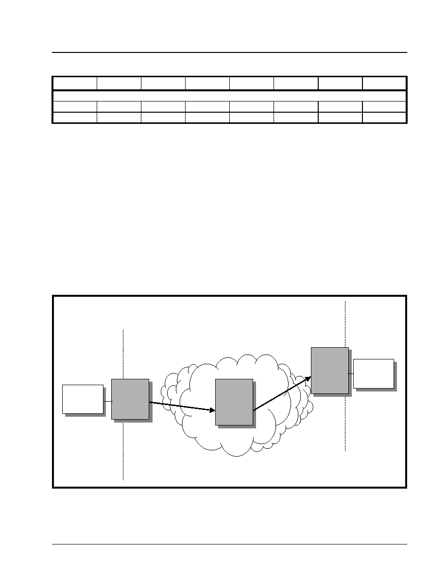
·Á
·Á
·Á
·Á
DS3/E3 FRAMER IC
XRT7250
REV. 1.1.1
197
When the µP reads these registers, it will read in the
number of parity-bit errors that have been detected by
the Receive DS3 Framer block, since the last time
these registers were read. These registers are reset
upon read.
N
OTE
: When the Framing with Parity option is selected, the
Receive DS3 Framer block will declared an OOF condition
if P-bit errors were detected in two out of 5 consecutive DS3
M-frames.
3.3.2.6.2 CP-Bit Checking/Options
CP-bits are very similar to P-bits except for the follow-
ing.
1. CP-bits are used to permit performance monitor-
ing over an entire DS3 path (e.g., from the source
terminal) through any number of mid-network ter-
minals to the sink terminal).
2. P-bits are used to permit performance monitoring
of a DS3 data stream, as it is transmitted from
one terminal to an adjacent terminal.
How CP-Bits are Processed
The following section describes how the CP-bits are
processed at three locations.
∑ The Source Terminal Equipment
∑ The Mid-Network Terminal Equipment
∑ The Sink Terminal Equipment
Figure_62 presents a simple illustration of the loca-
tions of these three types of Terminal Equipment,
within the Wide-Area Network.
N
OTE
: The use of the terms Source and Sink Terminal
Equipment are used to simplify this discussion of CP-Bit
Processing. In reality, the Source Terminal Equipment (in
Figure_62) will also function as the Sink Terminal Equip-
ment (for DS3 traffic traveling in the opposite direction).
Likewise, the Sink Terminal Equipment (in Figure_62) will
also function as the Source Terminal Equipment.
Processing at the Source Terminal Equipment
PMON PARITY ERROR EVENT COUNT REGISTER - LSB (ADDRESS = 0X55)
B
IT
7
B
IT
6
B
IT
5
B
IT
4
B
IT
3
B
IT
2
B
IT
1
B
IT
0
Parity Error Count - "Low" Byte
RO
RO
RO
RO
RO
RO
RO
RO
0
0
0
0
0
0
0
0
F
IGURE
82. A S
IMPLE
I
LLUSTRATION
OF
THE
L
OCATIONS
OF
THE
S
OURCE
, M
ID
-N
ETWORK
AND
S
INK
T
ERMINAL
E
QUIPMENT
(
FOR
CP-B
IT
P
ROCESSING
)
Source
Terminal
Equipment
Source
Terminal
Equipment
Sink
Terminal
Equipment
Sink
Terminal
Equipment
Mid-Network
Terminal
Equipment
Mid-Network
Terminal
Equipment
The Wide Area Network
Customer
Premises
Equipment
Customer
Premises
Equipment
Customer
Premises
Equipment
Customer
Premises
Equipment
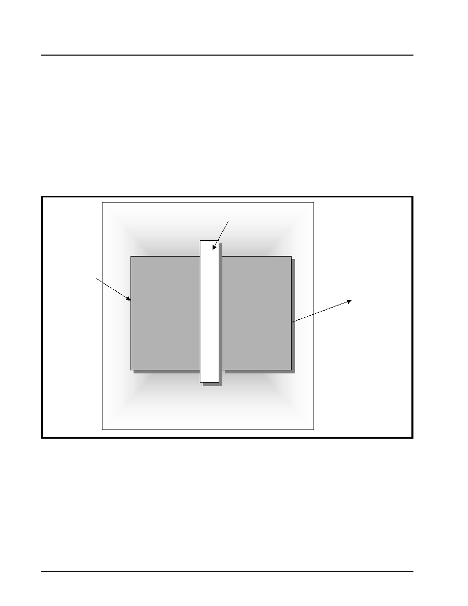
XRT7250
DS3/E3 FRAMER IC
·Á
·Á
·Á
·Á
REV. 1.1.1
198
The Source Terminal Equipment (located at one edge
of the wide-area network) will typically receive its DS3
payload data from some Customer Premise Equip-
ment (CPE). As the Source Terminal Equipment re-
ceives this data from the CPE, it will compute the
even-parity value over all bits within a given outbound
DS3 frame. The Terminal Equipment will then insert
this even parity value into both of the P-bit fields and
both of the CP-bits fields, within the very next out-
bound DS3 frame.
Hence, both the P-bit values and CP-bit values will
originate at the Source Terminal Equipment.
Processing at the Mid-Network Terminal Equip-
ment
The Mid-Network Terminal Equipment has the task of
doing the following.
∑ Receiving a DS3 data stream, via the Receive
WAN Interface Line Card.
∑ Transmitting this same DS3 data stream (out to
another Remote Terminal Equipment) via the
Transmit WAN Interface Line Card.
Figure 83 presents an illustration of the basic archi-
tecture of the Mid-Network Terminal Equipment.
Operation of the Receive WAN Interface Line Card
The Receive WAN Interface line card receives a DS3
data stream from some remote Terminal Equipment.
As the Receive WAN Interface card does this, it will
also do the following:
1. Compute and verify the "P-Bits" of each inbound
DS3 frame.
2. Compute and verify the "CP-Bits" of each
inbound DS3 frame.
3. Output both the payload and overhead bits to the
system back-plane.
Operation of the Transmit WAN Interface Line
Card
The Transmit WAN Interface Line Card receives the
outbound DS3 data stream from the system back-
plane. As the Transmit WAN Interface Line Card re-
ceives this data it will also do the following.
1. Extract out the "CP-bit" values, from the Receive
WAN Interface line card (via the system back-
plane) and insert these values into the CP-bit
fields, within the outbound DS3 data stream, via
the Transmit Overhead Data Input Interface block
of the XRT7250 Framer IC.
F
IGURE
83. I
LLUSTRATION
OF
THE
P
RESUMED
C
ONFIGURATION
OF
THE
M
ID
-N
ETWORK
T
ERMINAL
E
QUIPMENT
The Receiving
DS3 Line Card
The Receiving
DS3 Line Card
The Transmitting
DS3 Line Card
The Transmitting
DS3 Line Card
System Back-plane
DS3 Traffic
from "Source"
Terminal
Equipment
DS3 Traffic to
"Sink" Terminal
Equipment
The Mid-Network Terminal Equipment

·Á
·Á
·Á
·Á
DS3/E3 FRAMER IC
XRT7250
REV. 1.1.1
199
2. Compute the even-parity over all bits, within a
given outbound DS3 frame, and insert this value
into the "P" bits within the very next outbound
DS3 frame.
3. Transmit this resulting DS3 data stream to the
remote terminal equipment.
Processing at the Sink Terminal
The Sink Terminal Equipment (located at the opposite
edge of the wide-area-network, from the Source Ter-
minal Equipment) will receive and terminate this DS3
data stream. As the Sink Terminal Equipment re-
ceives this DS3 data stream it will also do the follow-
ing.
1. Compute and verify the "P"-bits within each
inbound DS3 frame.
2. Compute and verify the "CP" bits within each
inbound DS3 frame.
4.3.3
The Receive HDLC Controller Block
The Receive DS3 HDLC Controller block can be used
to receive either bit-oriented signaling (BOS) or mes-
sage-oriented signaling (MOS) type data link mes-
sages. The Receive DS3 HDLC Controller block can
also be configured to receive both types of message
from the remote terminal equipment.
Both BOS and MOS types of HDLC message pro-
cessing are discussed in detail below.
4.3.3.1
Bit-Oriented Signaling (or FEAC) Pro-
cessing via the Receive DS3 HDLC Controller.
The Receive DS3 HDLC Controller block consists of
two major sub-blocks
∑ The Receive FEAC Processor
∑ The LAPD Receiver
This section describes how to operate the Receive
FEAC Processor.
If the Receive DS3 Framer block is operating in the C-
bit Parity Framing format, then the FEAC bit-field
within the DS3 Frame can be used to receive FEAC
(Far End Alarm and Control) messages (See
Figure 84). Each FEAC code word is actually six bits
in length. However, this six bit FEAC Code word is
encapsulated with 10 framing bits to form a 16 bit
message of the form:
Where, [d5, d4, d3, d2, d1, d0] is the FEAC Code
word. The rightmost bit of the 16-bit data structure
(e.g., a 1) will be received first. Since each DS3
Frame contains only 1 FEAC bit-field, 16 DS3 Frames
are required to transmit the 16 bit FEAC code mes-
sage. The six bits, labeled "d5" through "d0" can rep-
resent 64 distinct messages, of which 43 have been
defined in the standards.
The Receive FEAC Processor frames and validates
the incoming FEAC data from the remote Transmit
FEAC Processor via the received FEAC channel. Ad-
ditionally, the Receive FEAC Processor will write the
Received FEAC code words into an 8 bit Rx-FEAC
register. Framing is performed by looking for two 0s
spaced 6 bits apart preceded by 8 1s. The Receive
DS3 HDLC Controller contains two registers that sup-
port FEAC Message Reception.
∑ Rx DS3 FEAC Register (Address = 0x16)
∑ Rx DS3 FEAC Interrupt Enable/Status Register
(Address = 0x17)
The Receive FEAC Processor generates an interrupt
upon validation and removal of the incoming FEAC
Code words.
Operation of the Receive DS3 FEAC Processor
The Receive FEAC Processor will validate or remove
FEAC code words that it receives from the remote
Transmit FEAC Processor. The FEAC Code Valida-
tion and Removal functions are described below.
FEAC Code Validation
When the remote terminal equipment wishes to send
a FEAC message to the Local Receive FEAC Proces-
sor, it (the remote terminal equipment) will transmit
this 16 bit message, repeatedly for a total of 10 times.
The Receive FEAC Processor will frame to this in-
coming FEAC Code Message, and will attempt to val-
idate this message. Once the Receive FEAC Proces-
sor has received the same FEAC code word in at
least 8 out of the last 10 received codes, it will vali-
date this code word by writing this 6 bit code word in-
to the Receive DS3 FEAC Register. The Receive
FEAC Processor will then inform the µC/µP of this
Receive FEAC validation event by generating a Rx
FEAC Valid interrupt and asserting the FEAC Valid
and the RxFEAC Valid Interrupt Status Bits in the Rx
DS3 Interrupt Enable/Status Register, as depicted
below. The Bit Format of the Rx DS3 FEAC Register
is presented below.
FEAC C
ODE
W
ORD
F
RAMING
0
d5
d4
d3
d2
d1
d0
0
1
1
1
1
1
1
1
1

XRT7250
DS3/E3 FRAMER IC
·Á
·Á
·Á
·Á
REV. 1.1.1
200
The bit-format of the Rx DS3 FEAC register is pre-
sented below. It is important to note that the last vali-
dated FEAC code word will be written into the shaded
bit-fields below.
The purpose of generating an interrupt to the µP, up-
on FEAC Code Word Validation is to inform the local
µP that the Framer has a newly received FEAC mes-
sage that needs to be read. The local µP would read-
in this FEAC code word from the Rx DS3 FEAC Reg-
ister (Address = 0x16).
FEAC Code Removal
After the 10th transmission of a given FEAC code
word, the remote terminal equipment may proceed to
transmit a different FEAC code word. When the Re-
ceive FEAC processor detects this occurrence, it
must Remove the FEAC codeword that is presently
residing in the Rx DS3 FEAC Register. The Receive
FEAC Processor will remove the existing FEAC code
word when it detects that 3 (or more) out of the last
10 received FEAC codes are different from the latest
validated FEAC code word. The Receive FEAC Pro-
cessor will inform the local µP/µC of this removal
event by generating a Rx FEAC Removal interrupt,
and asserting the RxFEAC Remove Interrupt Status
bit in the Rx DS3 Interrupt Enable/Status Register, as
depicted below.
Additionally, the Receive FEAC processor will also
denote the removal event by setting the FEAC Valid
bit-field (Bit 4), within the Rx DS3 FEAC Interrupt En-
able/Status Register to 0, as depicted above.
The description of Bits 0 through 3 within this register,
all support Interrupt Processing, and will therefore be
presented in Section 3.3.6. Figure 84 presents a flow
diagram depicting how the Receive FEAC Processor
functions.
RX DS3 FEAC INTERRUPT ENABLE/STATUS REGISTER (ADDRESS = 0X17)
B
IT
7
B
IT
6
B
IT
5
B
IT
4
B
IT
3
B
IT
2
B
IT
1
B
IT
0
Not Used
Not Used
Not Used
FEAC
Valid
RxFEAC
Remove
Interrupt
Enable
RxFEAC
Remove
Interrupt
status
RxFEAC
Valid
Interrupt
Enable
RxFEAC
Valid
Interrupt
Status
RO
RO
RO
RO
R/W
RUR
R/W
RUR
X
X
X
1
X
0
1
1
RX DS3 FEAC REGISTER (ADDRESS = 0X16)
B
IT
7
B
IT
6
B
IT
5
B
IT
4
B
IT
3
B
IT
2
B
IT
1
B
IT
0
Not Used
RxFEAC [5]
RxFEAC [4]
RxFEAC [3]
RxFEAC [2]
RxFEAC [1]
RxFEAC [0]
Not Used
RO
RO
RO
RO
RO
RO
RO
RO
0
d5
d4
d3
d2
d1
d0
0
RX DS3 FEAC INTERRUPT ENABLE/STATUS REGISTER (ADDRESS = 0X17)
B
IT
7
B
IT
6
B
IT
5
B
IT
4
B
IT
3
B
IT
2
B
IT
1
B
IT
0
Not Used
Not Used
Not Used
FEAC
Valid
RxFEAC
Remove
Interrupt
Enable
RxFEAC
Remove
Interrupt
status
RxFEAC
Valid
Interrupt
Enable
RxFEAC
Valid
Interrupt
Status
RO
RO
RO
RO
R/W
RUR
R/W
RUR
X
X
X
0
1
1
X
0
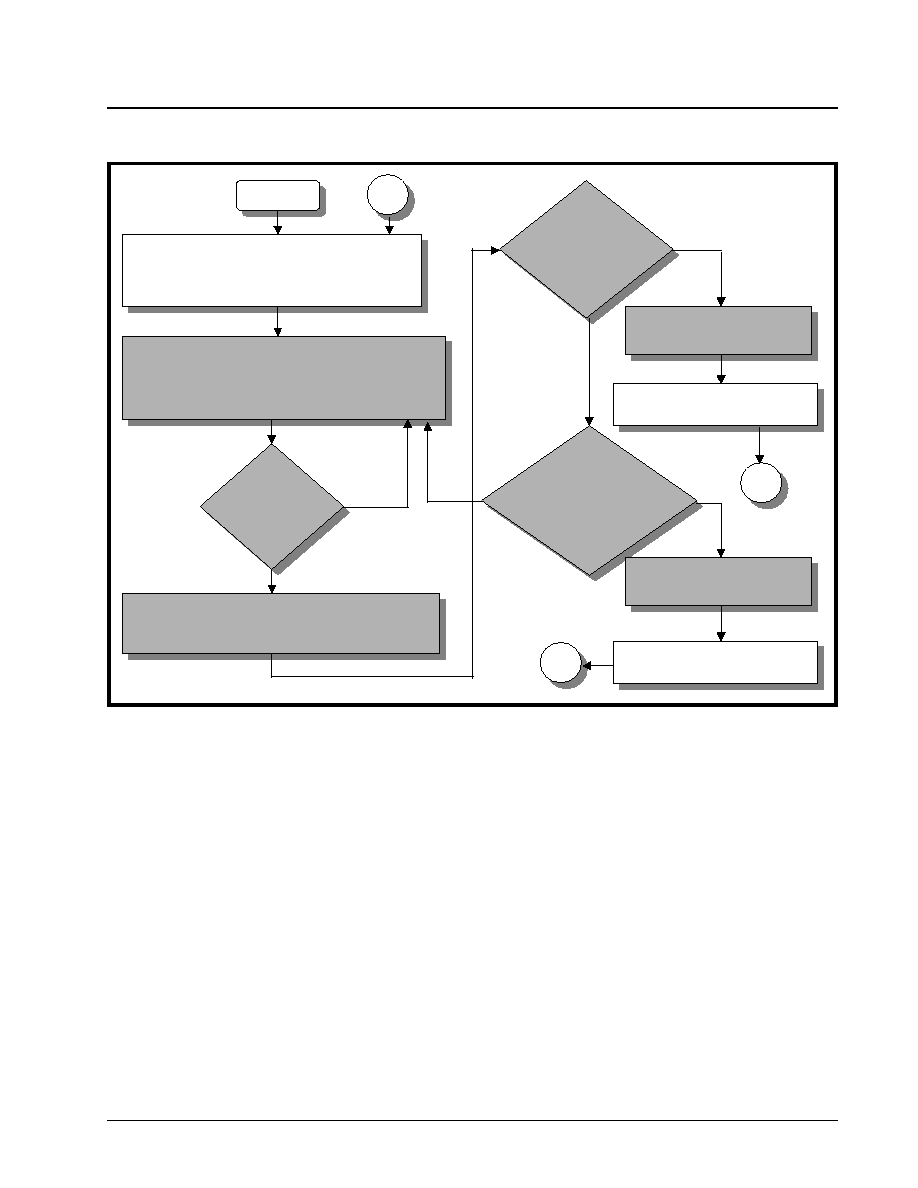
·Á
·Á
·Á
·Á
DS3/E3 FRAMER IC
XRT7250
REV. 1.1.1
201
N
OTES
:
1. The white (e.g., unshaded) boxes reflect tasks that
the user's system must perform in order to config-
ure the Receive FEAC Processor to receive FEAC
messages.
2. A brief description of the steps that must exist
within the FEAC Validation and FEAC Removal
Interrupt Service Routines exists in Section 3.6
4.3.3.2
The Message Oriented Signaling (e.g.,
LAP-D) Processing via the Receive DS3 HDLC
Controller block
The LAPD Receiver (within the Receive DS3 HDLC
Controller block) allows the user to receive PMDL
messages from the remote terminal equipment, via
the inbound DS3 frames. In this case, the inbound
message bits will be carried by the 3 DL bit-fields of
F-Frame 5, within each DS3 M-Frame. The remote
LAPD Transmitter will transmit a LAPD Message to
the Near-End Receiver via these three bits within
each DS3 Frame. The LAPD Receiver will receive
and store the information portion of the received
LAPD frame into the Receive LAPD Message Buffer,
which is located at addresses: 0xDE through 0x135
within the on-chip RAM. The LAPD Receiver has the
following responsibilities.
∑ Framing to the incoming LAPD Messages
∑ Filtering out stuffed 0s (within the information pay-
load)
∑ Storing the Frame Message into the Receive LAPD
Message Buffer
∑ Perform Frame Check Sequence (FCS) Verification
∑ Provide status indicators for
End of Message (EOM)
Flag Sequence Byte detected
Abort Sequence detected
Message Type
C/R Type
The occurrence of FCS Errors
F
IGURE
84. F
LOW
D
IAGRAM
DEPICTING
HOW
THE
R
ECEIVE
FEAC P
ROCESSOR
F
UNCTIONS
START
START
ENABLE THE "FEAC REMOVAL AND
"VALIDATION" INTERRUPTS.
This is accomplished by writing "xxxx 1010" into the
"RxDS3 FEAC Interrupt/Status Register (Address = 0x17)
ENABLE THE "FEAC REMOVAL AND
"VALIDATION" INTERRUPTS.
This is accomplished by writing "xxxx 1010" into the
"RxDS3 FEAC Interrupt/Status Register (Address = 0x17)
RECEIVE FEAC PROCESSOR BEGINS READING IN
THE FEAC BIT-FIELDS (OF INCOMING DS3 FRAMES)
The Receive FEAC Processor checks for the "FEAC Framing
Alignment" pattern of "01111110".
RECEIVE FEAC PROCESSOR BEGINS READING IN
THE FEAC BIT-FIELDS (OF INCOMING DS3 FRAMES)
The Receive FEAC Processor checks for the "FEAC Framing
Alignment" pattern of "01111110".
Is the
"FEAC Framing
Alignment"pattern
present in the FEAC
Channel
?
Is the
"FEAC Framing
Alignment"pattern
present in the FEAC
Channel
?
READ IN THE "6-BIT FEAC CODE WORD"
The 6-bit FEAC Code Word immediately follows the "FEAC
Framing Alignment" Pattern.
READ IN THE "6-BIT FEAC CODE WORD"
The 6-bit FEAC Code Word immediately follows the "FEAC
Framing Alignment" Pattern.
Has this
same FEAC
Code Word been
Received in 8 out of the last
10 FEAC Message
Receptions?
Has this
same FEAC
Code Word been
Received in 8 out of the last
10 FEAC Message
Receptions?
Has a FEAC
Code Word (other than
the last "Validated Code Word)
been Received in 3 out of the last
10 FEAC Message
Receptions?
Has a FEAC
Code Word (other than
the last "Validated Code Word)
been Received in 3 out of the last
10 FEAC Message
Receptions?
GENERATE "FEAC
VALIDATION" INTERRUPT
GENERATE "FEAC
VALIDATION" INTERRUPT
INVOKE "FEAC VALIDATION"
INTERRUPTSERVICE ROUTINE.
INVOKE "FEAC VALIDATION"
INTERRUPTSERVICE ROUTINE.
GENERATE "FEAC
REMOVAL" INTERRUPT
GENERATE "FEAC
REMOVAL" INTERRUPT
INVOKE "FEAC REMOVAL"
INTERRUPTSERVICE ROUTINE.
INVOKE "FEAC REMOVAL"
INTERRUPTSERVICE ROUTINE.
1
1
1
1
1
1
NO
YES
YES
NO
NO
YES
XRT7250
DS3/E3 FRAMER IC
·Á
·Á
·Á
·Á
REV. 1.1.1
202
The LAPD receiver's actions are facilitated via the fol-
lowing two registers.
∑ Rx DS3 LAPD Control Register
∑ Rx DS3 LAPD Status Register
Operation of the LAPD Receiver
The LAPD Receiver, once enabled, will begin search-
ing for the boundaries of the incoming LAPD mes-
sage. The LAPD Message Frame boundaries are de-
lineated via the Flag Sequence octets (0x7E), as de-
picted in Figure 85.
Where: Flag Sequence = 0x7E
SAPI + CR + EA = 0x3C or 0x3E
TEI + EA = 0x01
Control = 0x03
The 16 bit FCS is calculated using CRC-16, x16 +
x12 + x5 + 1
The microprocessor/microcontroller (at the remote
terminal), while assembling the LAPD Message
frame, will insert an additional byte at the beginning of
the information (payload) field. This first byte of the
information field indicates the type and size of the
message being transferred. The value of this infor-
mation field and the corresponding message type/
size follow:
CL Path Identification = 0x38 (76 bytes)
IDLE Signal Identification = 0x34 (76 bytes)
Test Signal Identification = 0x32 (76 bytes)
ITU-T Path Identification = 0x3F (82 bytes)
The LAPD Receiver must be enabled before it can
begin receiving any LAPD messages. The LAPD Re-
ceiver can be enabled by writing a "1" into Bit 2 (Rx-
LAPD Enable) within the Rx DS3 LAPD Control Reg-
ister. The bit format of this register is depicted below.
Once the LAPD Receiver has been enabled, it will be-
gin searching for the Flag Sequence octets (0x7E), in
the DL bit-fields, within the incoming DS3 frames.
When the LAPD Receiver finds the flag sequence
byte, it will assert the Flag Present bit (Bit 0) within
the Rx DS3 LAPD Status Register, as depicted be-
low.
F
IGURE
85. LAPD M
ESSAGE
F
RAME
F
ORMAT
Flag Sequence (8 bits)
SAPI (6-bits)
C/R
EA
TEI (7 bits)
EA
Control (8-bits)
76 or 82 Bytes of Information (Payload)
FCS - MSB
FCS - LSB
Flag Sequence (8-bits)
RX DS3 LAPD CONTROL REGISTER (ADDRESS = 0X18)
B
IT
7
B
IT
6
B
IT
5
B
IT
4
B
IT
3
B
IT
2
B
IT
1
B
IT
0
Not Used
Not Used
Not Used
Not Used
Not Used
RxLAPD
Enable
RxLAPD
Interrupt
Enable
RxLAPD
Interrupt
Status
RO
RO
RO
RO
RO
R/W
R/W
RUR
0
0
0
0
0
1
X
X
RX DS3 LAPD STATUS REGISTER (ADDRESS = 0X19)
B
IT
7
B
IT
6
B
IT
5
B
IT
4
B
IT
3
B
IT
2
B
IT
1
B
IT
0
Not Used
RxAbort
RxLAPD Type[1, 0]
RxCR Type
RxFCS Error
End of
Message
Flag
Present
X
X
X
X
X
X
X
1

·Á
·Á
·Á
·Á
DS3/E3 FRAMER IC
XRT7250
REV. 1.1.1
203
The receipt of the Flag Sequence octet can mean
one of two things.
1. The Flag Sequence byte marks the beginning or
end of an incoming LAPD Message.
2. The received Flag Sequence octet could be just
one of many Flag Sequence octets that are trans-
mitted via the DS3 Transport Medium, during idle
periods between the transmission of LAPD Mes-
sages.
The LAPD Receiver will clear the Flag Present bit as
soon as it has received an octet that is something
other than the Flag Sequence octet. At this point, the
LAPD Receiver should be receiving either octet #2 of
the incoming LAPD Message, or an Abort Sequence
(e.g., a string of seven or more consecutive 1s). If
this next set of data is an abort sequence, then the
LAPD Receiver will assert the RxAbort bit (Bit 6) with-
in the Rx DS3 LAPD Status Register. However, if this
next octet is Octet #2 of an incoming LAPD Message,
then the Rx DS3 LAPD Status Register will begin to
present some additional status information on this in-
coming message. Each of these indicators is pre-
sented below in sequential order.
Bit 3 - RxCR Type - C/R (Command/Response)
Type
This bit-field reflects the contents of the C/R bit-field
within octet #2 of the LAPD Frame Header. When
this bit is "0" it means that this message is originating
from a customer installation. When this bit is "1" it
means that this message is originating from a net-
work terminal.
Bit 4,5 - RxLAPD Type[1, 0] - LAPD Message Type
The combination of these two bit fields indicate the
Message Type and the Message Size of the incoming
LAPD Message frame. Table 40 relates the values of
Bits 4 and 5 to the Incoming LAPD Message Type/
Size.
N
OTE
: The Message Size pertains to the size of the Infor-
mation portion of the LAPD Message Frame (as presented
in Figure 85).
Bit 3 - Flag Present
The LAPD Receiver should receive another Flag Se-
quence octet, which marks the End of the Message.
Therefore, this bit field should be asserted once
again.
Bit 1 - EndOfMessage - End of LAPD Message
Frame
Upon receipt of the closing Flag Sequence octet, this
bit-field should be asserted. The assertion of this bit-
field indicates that a LAPD Message Frame has been
completely received. Additionally, if this newly re-
ceived LAPD Message is different from the previous
message, then the LAPD Receiver will inform the µC/
µP of the EndOfMessage event by generating an in-
terrupt.
Bit 2 - RxFCSErr - Frame Check Sequence Error
Indicator
The LAPD Receiver will take the incoming LAPD
Message and compute its own version of the Frame
Check Sequence (FCS) word. Afterwards, the LAPD
Receiver will compare its computed value with that it
has received from the remote LAPD Transmitter. If
these two values match, then the LAPD Receiver will
presume that the LAPD Message has been properly
received and the contents of the Received LAPD
Message (payload portion) will be retained at loca-
tions 0xDE through 0x135 in on-chip RAM. The
LAPD Receiver will indicate an error-free reception of
the LAPD Message by keeping this bit field negated
(Bit 2 = 0). However, if these two FCS values do not
match, then the received LAPD Message is corrupted
and the user is advised not to process this erroneous
information. The LAPD Receiver will indicate an erred
receipt of this message by setting this bit-field to 1.
N
OTE
: The Receive DS3 HDLC Controller block will not
generate an interrupt to the
µP
due to the detection of an
FCS error. Therefore, the user is advised to validate each
and every received LAPD message by checking this bit-
field prior to processing the LAPD message.
Removal of Stuff Bits from the Payload Portion of
the incoming LAPD Message
While the LAPD Receiver is receiving a LAPD Mes-
sage, it has the responsibility of removing all of the
"0" stuff bits from the Payload Portion of the incoming
LAPD Message Frame. Recall that the text in Section
3.2.3.2 indicated that the LAPD Transmitter (at the re-
T
ABLE
40: T
HE
R
ELATIONSHIP
BETWEEN
R
X
LAPDT
YPE
[1:0]
AND
THE
RESULTING
LAPD M
ESSAGE
TYPE
AND
SIZE
R
X
LAPD T
YPE
[1, 0]
M
ESSAGE
T
YPE
M
ESSAGE
S
IZE
00
Test Signal Identification
76 bytes
01
Idle Signal Identification
76 bytes
10
CL Path Identification
76 bytes
11
TU-T Path Identification
82 bytes
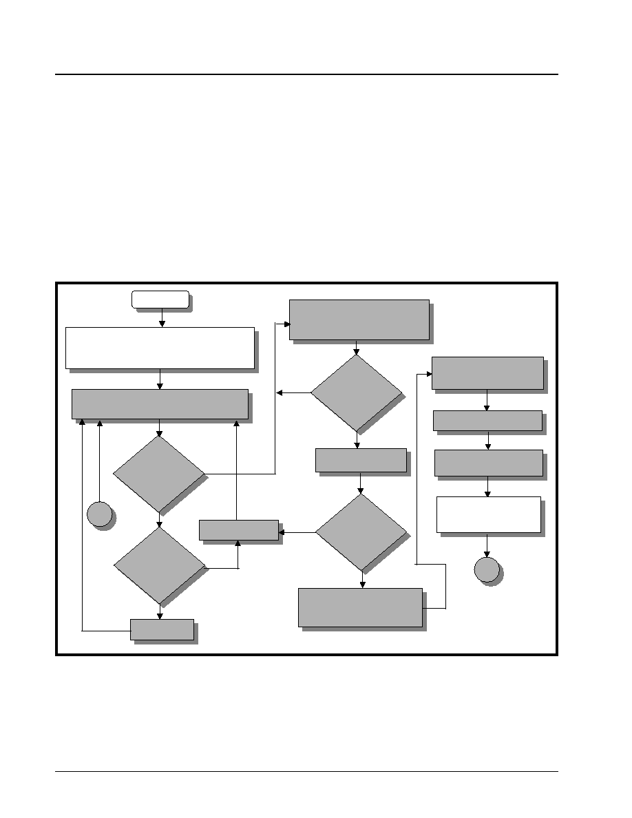
XRT7250
DS3/E3 FRAMER IC
·Á
·Á
·Á
·Á
REV. 1.1.1
204
mote terminal) will insert a "0" immediately following a
string of 5 consecutive 1s within the payload portion
of the LAPD Message frame. The LAPD Transmitter
performs this bit-stuffing procedure in order to prevent
the user data from mimicking the Flag Sequence oc-
tet (0x7E) or the ABORT sequence. Therefore, in or-
der to recover the user data to its original content (pri-
or to the bit-stuffing), the LAPD Receiver will remove
the "0" that immediately follows a string of 5 consecu-
tive 1s.
Writing the Incoming LAPD Message into the Re-
ceive LAPD Message Buffer
The LAPD receiver will obtain the LAPD Message
frame from the incoming DS3 data-stream. In addi-
tion to processing the framing overhead octets, per-
forming error checking (via FCS) and removing the
stuffed 0s from the user payload data. The LAPD Re-
ceiver will also write the payload portion of the LAPD
Frame into the Receive LAPD Message buffer at lo-
cations 0xDE through 0x135 in on-chip RAM.
Therefore, the local µP/µC must read this location
when it wishes to process this newly received LAPD
Message.
Figure 86 presents a flow chart depicting how the
LAPD Receiver works.
N
OTES
:
1. The white (e.g., unshaded) boxes reflect tasks that
the user's system must perform in order to config-
ure the LAPD Receiver to receive LAPD Messages.
2. A brief description of the steps that must exist
within the Receive LAPD Interrupt Service routine
exists in Section 3.3.6.
4.3.4
The Receive Overhead Data Output Inter-
face
Figure 87 presents a simple illustration of the Receive
Overhead Data Output Interface block within the
XRT7250.
F
IGURE
86. F
LOW
C
HART
DEPICTING
THE
F
UNCTIONALITY
OF
THE
LAPD R
ECEIVER
START
START
ENABLE THE LAPD RECEIVER
This is done by writing the value "0xFC into the
RxLAPD Control Register (Address = 0x18)
LAPD Receiver begins reading in the DL bits
from each inbound DS3 frame
Does
the LAPD
Receiver detect 6
consecutive
Zeros
?
Does
the LAPD
Receiver detect 6
consecutive
Zeros
?
Does
the LAPD
Receiver detect 7
consecutive
Zeros
?
Does
the LAPD
Receiver detect 7
consecutive
Zeros
?
Flag Sequence
Flag Sequence
ABORT Sequence
ABORT Sequence
LAPD Receiver is reading in a LAPD
Message Frame, containing a PMDL
Message.
LAPD Receiver is reading in a LAPD
Message Frame, containing a PMDL
Message.
Does
the LAPD
Receiver detect 6
consecutive
Zeros
?
Does
the LAPD
Receiver detect 6
consecutive
Zeros
?
Does
the LAPD
Receiver detect 7
consecutive
Zeros
?
Does
the LAPD
Receiver detect 7
consecutive
Zeros
?
End of Message (EOM)
End of Message (EOM)
VERIFY THE FCS VALUE
Report results in the RxLAPD
Status Register..
VERIFY THE FCS VALUE
Report results in the RxLAPD
Status Register..
"Un-stuff contents of Received
Message"
"Un-stuff contents of Received
Message"
Write Received PMDL Message
into the Receive LAPD Message
Buffer (Addresses 0xDE - 0x135)
Write Received PMDL Message
into the Receive LAPD Message
Buffer (Addresses 0xDE - 0x135)
Generate "Received LAPD
Interrupt"
Generate "Received LAPD
Interrupt"
Execute Receive LAPD
Interrupt Service Routine
Execute Receive LAPD
Interrupt Service Routine
1
1
1
1
NO
YES
NO
YES
YES
NO
YES
NO

·Á
·Á
·Á
·Á
DS3/E3 FRAMER IC
XRT7250
REV. 1.1.1
205
The DS3 frame consists of 4760 bits. Of these bits,
4704 bits are payload bits and the remaining 56 bits
are overhead bits. The XRT7250 has been designed
to handle and process both the payload type and
overhead type bits for each DS3 frame.
The Receive Payload Data Output Interface block,
within the Receive Section of the XRT7250, has
been designed to handle the payload bits. Likewise,
the Receive Overhead Data Output Interface block
has been designed to handle and process the over-
head bits.
The Receive Overhead Data Output Interface block
unconditionally outputs the contents of all overhead
bits within the incoming DS3 data stream. The
XRT7250 does not offer the user a means to shut off
this transmission of data. However, the Receive
Overhead Output Interface block does provide the us-
er with the appropriate output signals for external Da-
ta Link Layer equipment to sample and process these
overhead bits, via the following two methods.
∑ Method 1- Using the RxOHClk clock signal.
∑ Method 2 - Using the RxClk and RxOHEnable out-
put signals.
Each of these methods are described below.
4.3.4.1
Method 1 - Using the RxOHClk Clock
signal
The Receive Overhead Data Output Interface block
consists of four (4) signals. Of these four signals, the
following three signals are to be used when sampling
the DS3 overhead bits via Method 1.
∑ RxOH
∑ RxOHClk
∑ RxOHFrame
Each of these signals are listed and described below
in Table 41.
F
IGURE
87. A S
IMPLE
I
LLUSTRATION
OF
THE
R
ECEIVE
O
VERHEAD
O
UTPUT
I
NTERFACE
BLOCK
Receive Overhead
Output Interface
Block
Receive Overhead
Output Interface
Block
From Receive
DS3 Framer Block
RxOHFrame
RxOH
RxOHClk
RxOHEnable

XRT7250
DS3/E3 FRAMER IC
·Á
·Á
·Á
·Á
REV. 1.1.1
206
Interfacing the Receive Overhead Data Output In-
terface block to the Terminal Equipment (Method
1)
Figure 88 illustrates how one should interface the Re-
ceive Overhead Data Output Interface block to the
Terminal Equipment when using Method 1 to sample
and process the overhead bits from the inbound DS3
data stream.
T
ABLE
41: L
ISTING
AND
D
ESCRIPTION
OF
THE
P
IN
A
SSOCIATED
WITH
THE
R
ECEIVE
O
VERHEAD
D
ATA
O
UTPUT
I
NTERFACE
B
LOCK
S
IGNAL
N
AME
T
YPE
D
ESCRIPTION
RxOH
Output
Receive Overhead Data Output pin:
The XRT7250 will output the overhead bits, within the incoming DS3 frames, via this pin.
The Receive Overhead Data Output Interface block will output a given overhead bit, upon the
falling edge of RxOHClk. Hence, the external data link equipment should sample the data, at
this pin, upon the rising edge of RxOHClk.
The XRT7250 will always output the DS3 Overhead bits via this output pin. There are no
external input pins or register bit settings available that will disable this output pin.
RxOHClk
Output
Receive Overhead Data Output Interface Clock Signal:
The XRT7250 will output the Overhead bits (within the incoming DS3 frames), via the RxOH
output pin, upon the falling edge of this clock signal.
As a consequence, the user's data link equipment should use the rising edge of this clock sig-
nal to sample the data on both the RxOH and RxOHFrame output pins.
This clock signal is always active.
RxOHFrame
Output
Receive Overhead Data Output Interface - Start of Frame Indicator:
The XRT7250 will drive this output pin "High" (for one period of the RxOHClk signal), when-
ever the first overhead bit within a given DS3 frame is being driven onto the RxOH output pin.

·Á
·Á
·Á
·Á
DS3/E3 FRAMER IC
XRT7250
REV. 1.1.1
207
Method 1 Operation of the Terminal Equipment
If the Terminal Equipment intends to sample any
overhead data from the inbound DS3 data stream (via
the Receive Overhead Data Output Interface block)
then it is expected to do the following:
1. Sample the state of the RxOHFrame signal (e.g.,
the Rx_Start_of_Frame input signal) on the rising
edge of the RxOHClk (e.g., the
DS3_OH_Clock_In) signal.
2. Keep track of the number of rising clock edges
that have occurred in the RxOHClk (e.g., the
DS3_OH_Clock_In) signal, since the last time the
RxOHFrame signal was sampled "High". By
doing this, the Terminal Equipment will be able to
keep track of which overhead bit is being output
via the RxOH output pin. Based upon this infor-
mation, the Terminal Equipment will be able to
derive some meaning from these overhead bits.
Table 42 relates the number of rising clock edges (in
the RxOHClk signal, since the RxOHFrame signal
was last sampled "High") to the DS3 Overhead bit
that is being output via the RxOH output pin.
F
IGURE
88. I
LLUSTRATION
OF
HOW
TO
INTERFACE
THE
T
ERMINAL
E
QUIPMENT
TO
THE
R
ECEIVE
O
VERHEAD
D
ATA
O
UTPUT
I
NTERFACE
BLOCK
(
FOR
M
ETHOD
1).
Terminal Equipment
XRT7250 DS3 Framer IC
RxOHClk
DS3_OH_Clock_In
RxOH
RxOHFrame
DS3_OH_In
Rx_Start_of_Frame

XRT7250
DS3/E3 FRAMER IC
·Á
·Á
·Á
·Á
REV. 1.1.1
208
T
ABLE
42: T
HE
R
ELATIONSHIP
BETWEEN
THE
N
UMBER
OF
R
ISING
C
LOCK
E
DGES
IN
R
X
OHC
LK
, (
SINCE
R
X
OHF
RAME
WAS
LAST
SAMPLED
"H
IGH
")
TO
THE
DS3 O
VERHEAD
B
IT
,
THAT
IS
BEING
OUTPUT
VIA
THE
R
X
OH
OUTPUT
PIN
N
UMBER
OF
R
ISING
C
LOCK
E
DGES
IN
R
X
OHC
LK
T
HE
O
VERHEAD
B
IT
BEING
OUTPUT
BY
THE
XRT7250
0 (Clock edge is coincident with RxOHFrame being detected "High")
X
1
F1
2
AIC
3
F0
4
NA
5
F0
6
FEAC
7
F1
8
X
9
F1
10
UDL
11
F0
12
UDL
13
F0
14
UDL
15
F1
16
P
17
F1
18
CP
19
F0
20
CP
21
F0
22
CP
23
F1
24
P
25
F1
26
FEBE
27
F0
28
FEBE
29
F0
30
FEBE
31
F1
32
M0
33
F1
34
DL
35
F0
36
DL
37
F0

·Á
·Á
·Á
·Á
DS3/E3 FRAMER IC
XRT7250
REV. 1.1.1
209
Figure 89 presents the typical behavior of the Re-
ceive Overhead Data Output Interface block, when
Method 1 is being used to sample the incoming DS3
overhead bits.
38
DL
39
F1
40
M1
41
F1
42
UDL
43
FO
44
UDL
45
FO
46
UDL
47
F1
48
M0
49
F1
50
UDL
51
F0
52
UDL
53
F0
54
UDL
55
F1
T
ABLE
42: T
HE
R
ELATIONSHIP
BETWEEN
THE
N
UMBER
OF
R
ISING
C
LOCK
E
DGES
IN
R
X
OHC
LK
, (
SINCE
R
X
OHF
RAME
WAS
LAST
SAMPLED
"H
IGH
")
TO
THE
DS3 O
VERHEAD
B
IT
,
THAT
IS
BEING
OUTPUT
VIA
THE
R
X
OH
OUTPUT
PIN
N
UMBER
OF
R
ISING
C
LOCK
E
DGES
IN
R
X
OHC
LK
T
HE
O
VERHEAD
B
IT
BEING
OUTPUT
BY
THE
XRT7250
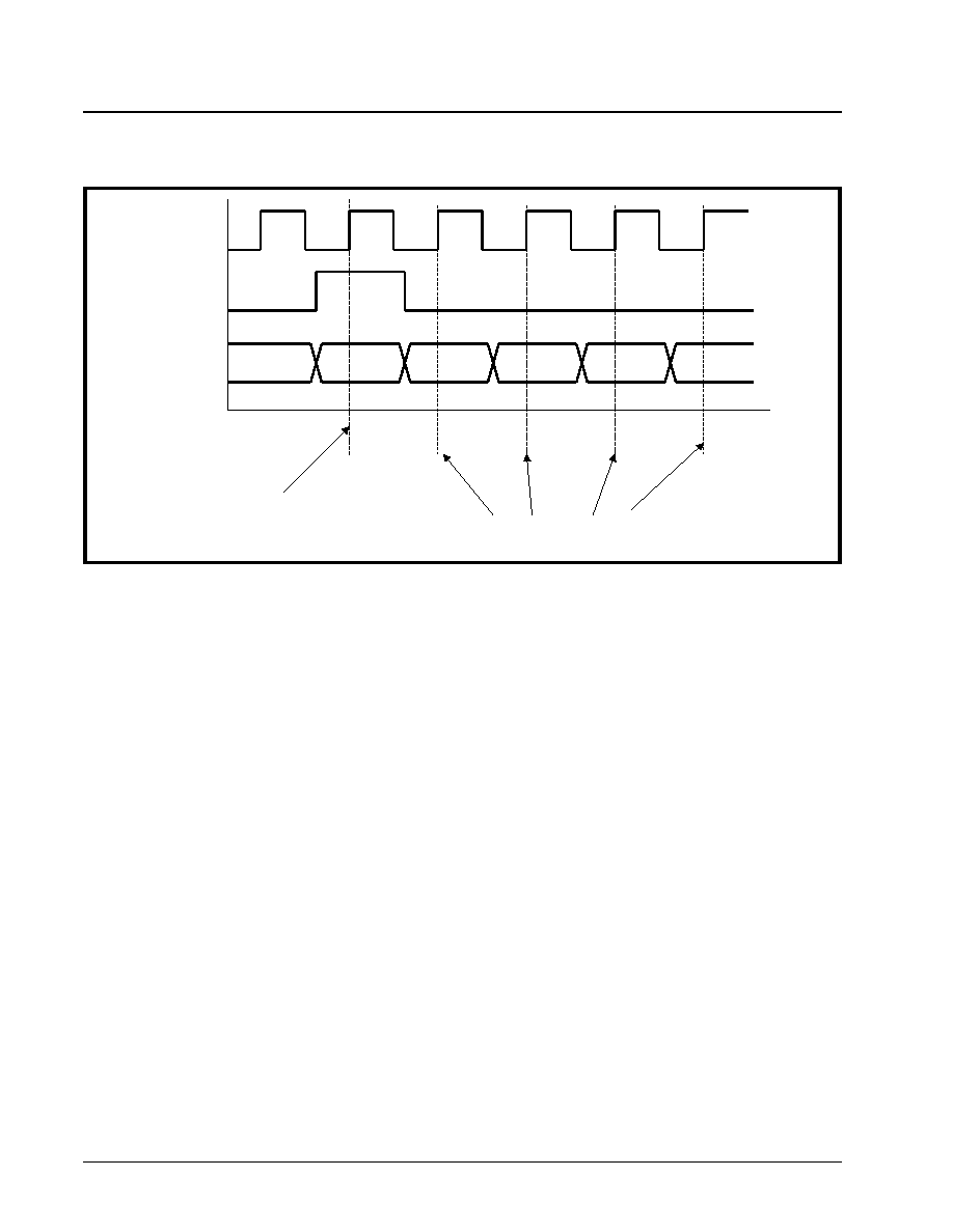
XRT7250
DS3/E3 FRAMER IC
·Á
·Á
·Á
·Á
REV. 1.1.1
210
Method 2 - Using RxOutClk and the RxOHEnable
signals
Method 1 requires that the Terminal Equipment be
able to handle an additional clock signal, RxOHClk.
However, there may be a situation in which the Termi-
nal Equipment circuitry does not have the means to
accommodate and process this extra clock signal, in
order to use the Receive Overhead Data Output Inter-
face. Hence, Method 2 is available. Method 2 in-
volves the use of the following signals.
∑ RxOH
∑ RxOutClk
∑ RxOHEnable
∑ RxOHFrame
Each of these signals are listed and described below
in Table 43.
F
IGURE
89. I
LLUSTRATION
OF
THE
SIGNALS
THAT
ARE
OUTPUT
VIA
THE
R
ECEIVE
O
VERHEAD
O
UTPUT
I
NTERFACE
(
FOR
M
ETHOD
1).
RxOHClk
RxOHFrame
RxOH
X F1 AIC F0 FEAC
Terminal Equipment should sample
the "RxOHFrame" and "RxOH" signals
here.
Recommended Sampling Edges

·Á
·Á
·Á
·Á
DS3/E3 FRAMER IC
XRT7250
REV. 1.1.1
211
Interfacing the Receive Overhead Data Output In-
terface block to the Terminal Equipment (Method
2)
Figure 90 illustrates how one should interface the Re-
ceive Overhead Data Output Interface block to the
Terminal Equipment, when using Method 2 to sample
and process the overhead bits from the inbound DS3
data stream.
T
ABLE
43: L
ISTING
AND
D
ESCRIPTION
OF
THE
P
IN
A
SSOCIATED
WITH
THE
R
ECEIVE
O
VERHEAD
D
ATA
O
UTPUT
I
NTERFACE
B
LOCK
(M
ETHOD
2)
S
IGNAL
N
AME
T
YPE
D
ESCRIPTION
RxOH
Output
Receive Overhead Data Output pin:
The XRT7250 will output the overhead bits, within the incoming DS3 frames, via this pin.
The Receive Overhead Output Interface will pulse the RxOHEnable output pin (for one RxOut-
Clk period) at approximately the middle of the RxOH bit period. The user is advised to design
the Terminal Equipment to latch the contents of the RxOH output pin, whenever the RxOHEn-
able output pin is sampled "High" on the falling edge of RxOutClk.
RxOHEnable
Output
Receive Overhead Data Output Enable - Output pin:
The XRT7250 will assert this output signal for one RxOutClk period when it is safe for the Ter-
minal Equipment to sample the data on the RxOH output pin.
RxOHFrame
Output
Receive Overhead Data Output Interface - Start of Frame Indicator:
The XRT7250 will drive this output pin "High" (for one period of the RxOH signal), whenever
the first overhead bit, within a given DS3 frame is being driven onto the RxOH output pin.
RxOutClk
Output
Receive Section Output Clock Signal:
This clock signal is derived from the RxLineClk signal (from the LIU) for loop-timing applica-
tions, and the TxInClk signal (from a local oscillator) for local-timing applications. For DS3
applications, this clock signal will operate at 44.736MHz.
The user is advised to design the Terminal Equipment to latch the contents of the RxOH pin,
anytime the RxOHEnable output signal is sampled "High" on the falling edge of this clock sig-
nal.
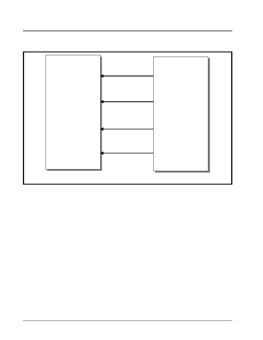
XRT7250
DS3/E3 FRAMER IC
·Á
·Á
·Á
·Á
REV. 1.1.1
212
Method 2 Operation of the Terminal Equipment
If the Terminal Equipment intends to sample any
overhead data from the inbound DS3 data stream (via
the Receive Overhead Data Output Interface), then it
is expected to do the following.
1. Sample the state of the RxOHFrame signal (e.g.,
the Rx_Start_of_Frame input) on the falling edge
of the RxOutClk clock signal, whenever the RxO-
HEnable output signal is also sampled "High".
2. Keep track of the number of times that the RxO-
HEnable signal has been sampled "High" since
the last time the RxOHFrame was also sampled
"High". By doing this, the Terminal Equipment
will be able to keep track of which overhead bit is
being output via the RxOH output pin. Based
upon this information, the Terminal Equipment
will be able to derive some meaning from these
overhead bits.
3. Table 44 relates the number of RxOHEnable out-
put pulses (that have occurred since both the
RxOHFrame and the RxOHEnable pins were
both sampled "High") to the DS3 overhead bit
that is being output via the RxOH output pin.
F
IGURE
90. I
LLUSTRATION
OF
HOW
TO
INTERFACE
THE
T
ERMINAL
E
QUIPMENT
TO
THE
R
ECEIVE
O
VERHEAD
D
ATA
O
UTPUT
I
NTERFACE
BLOCK
(
FOR
M
ETHOD
2).
RxOH
RxOHEnable
RxOutClk
RxOHFrame
DS3_OH_In
DS3_OH_Enable_In
DS3_Clk_In
Rx_Start_of_Frame
Terminal Equipment
XRT7250 DS3 Framer IC

·Á
·Á
·Á
·Á
DS3/E3 FRAMER IC
XRT7250
REV. 1.1.1
213
T
ABLE
44: T
HE
R
ELATIONSHIP
BETWEEN
THE
N
UMBER
OF
R
X
OHE
NABLE
OUTPUT
PULSES
((
SINCE
R
X
OHF
RAME
WAS
LAST
SAMPLED
"H
IGH
")
TO
THE
DS3 O
VERHEAD
B
IT
,
THAT
IS
BEING
OUTPUT
VIA
THE
R
X
OH
OUTPUT
PIN
N
UMBER
OF
R
X
OHE
NABLE
O
UTPUT
P
ULSES
T
HE
O
VERHEAD
B
IT
BEING
OUTPUT
BY
THE
XRT7250
0 (The RxOHEnable and RxOHFrame signals are both sampled "High")
X
1
F1
2
AIC
3
F0
4
NA
5
F0
6
FEAC
7
F1
8
X
9
F1
10
UDL
11
F0
12
UDL
13
F0
14
UDL
15
F1
16
P
17
F1
18
CP
19
F0
20
CP
21
F0
22
CP
23
F1
24
P
25
F1
26
FEBE
27
F0
28
FEBE
29
F0
30
FEBE
31
F1
32
M0
33
F1
34
DL
35
F0
36
DL
37
F0
38
DL

XRT7250
DS3/E3 FRAMER IC
·Á
·Á
·Á
·Á
REV. 1.1.1
214
Figure 91 presents the typical behavior of the Re-
ceive Overhead Data Output Interface block, when
Method 2 is being used to sample the incoming DS3
overhead bits.
39
F1
40
M1
41
F1
42
UDL
43
FO
44
UDL
45
FO
46
UDL
47
F1
48
M0
49
F1
50
UDL
51
F0
52
UDL
53
F0
54
UDL
55
F1
T
ABLE
44: T
HE
R
ELATIONSHIP
BETWEEN
THE
N
UMBER
OF
R
X
OHE
NABLE
OUTPUT
PULSES
((
SINCE
R
X
OHF
RAME
WAS
LAST
SAMPLED
"H
IGH
")
TO
THE
DS3 O
VERHEAD
B
IT
,
THAT
IS
BEING
OUTPUT
VIA
THE
R
X
OH
OUTPUT
PIN
N
UMBER
OF
R
X
OHE
NABLE
O
UTPUT
P
ULSES
T
HE
O
VERHEAD
B
IT
BEING
OUTPUT
BY
THE
XRT7250
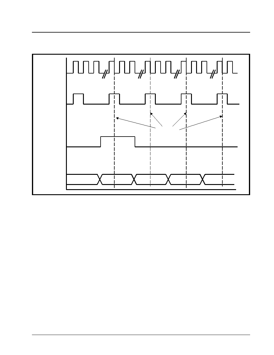
·Á
·Á
·Á
·Á
DS3/E3 FRAMER IC
XRT7250
REV. 1.1.1
215
4.3.5
The Receive Payload Data Output Inter-
face
Figure 92 presents a simple illustration of the Receive
Payload Data Output Interface block.
F
IGURE
91. I
LLUSTRATION
OF
THE
SIGNALS
THAT
ARE
OUTPUT
VIA
THE
R
ECEIVE
O
VERHEAD
D
ATA
O
UTPUT
I
NTER
-
FACE
BLOCK
(
FOR
M
ETHOD
2).
RxOutClk
RxOHEnable
RxOHFrame
RxOH
F1 X F1 AIC F0
Recommended
Sampling
Edges

XRT7250
DS3/E3 FRAMER IC
·Á
·Á
·Á
·Á
REV. 1.1.1
216
Each of the output pins of the Receive Payload Data
Output Interface block are listed in Table 45 and de-
scribed below. The exact role that each of these out-
put pins assume, for a variety of operating scenarios
are described throughout this section.
F
IGURE
92. A S
IMPLE
ILLUSTRATION
OF
THE
R
ECEIVE
P
AYLOAD
D
ATA
O
UTPUT
I
NTERFACE
BLOCK
Receive Payload
Data Output
Interface
Receive Payload
Data Output
Interface
RxOHInd
RxSer
RxNib[3:0]
RxClk
RxOutClk
RxFrame
From Receive DS3
Framer Block

·Á
·Á
·Á
·Á
DS3/E3 FRAMER IC
XRT7250
REV. 1.1.1
217
T
ABLE
45: L
ISTING
AND
D
ESCRIPTION
OF
THE
PIN
ASSOCIATED
WITH
THE
R
ECEIVE
P
AYLOAD
D
ATA
O
UTPUT
I
NTERFACE
BLOCK
S
IGNAL
N
AME
T
YPE
D
ESCRIPTION
RxSer
Output Receive Serial Payload Data Output pin:
If the user opts to operate the XRT7250 in the serial mode, then the chip will output the payload
data, of the incoming DS3 frames, via this pin. The XRT7250 will output this data upon the rising
edge of RxClk.
The user is advised to design the Terminal Equipment such that it will sample this data on the
falling edge of RxClk.
This signal is only active if the NibInt input pin is pulled "Low".
RxNib[3:0]
Output Receive Nibble-Parallel Payload Data Output pins:
If the user opts to operate the XRT7250 in the nibble-parallel mode, then the chip will output the
payload data, of the incoming DS3 frames, via these pins. The XRT7250 will output data via
these pins, upon the falling edge of the RxClk output pin.
The user is advised to design the Terminal Equipment such that it will sample this data upon the
rising edge of RxClk.
These pins are only active if the NibInt input pin is pulled "High".
RxClk
Output Receive Payload Data Output Clock pin:
The exact behavior of this signal depends upon whether the XRT7250 is operating in the Serial
or in the Nibble-Parallel-Mode.
Serial Mode Operation
In the serial mode, this signal is a 44.736MHz clock output signal. The Receive Payload Data
Output Interface will update the data via the RxSer output pin, upon the rising edge of this clock
signal.
The user is advised to design (or configure) the Terminal Equipment to sample the data on the
RxSer pin, upon the falling edge of this clock signal.
Nibble-Parallel Mode Operation
In this Nibble-Parallel Mode, the XRT7250 will derive this clock signal, from the RxLineClk signal.
The XRT7250 will pulse this clock 1176 times for each inbound DS3 frame. The Receive Pay-
load Data Output Interface will update the data, on the RxNib[3:0] output pins upon the falling
edge of this clock signal.
The user is advised to design (or configure) the Terminal Equipment to sample the data on the
RxNib[3:0] output pins, upon the rising edge of this clock signal
RxOHInd
Output Receive Overhead Bit Indicator Output:
This output pin will pulse "High" whenever the Receive Payload Data Output Interface outputs an
overhead bit via the RxSer output pin. The purpose of this output pin is to alert the Terminal
Equipment that the current bit, (which is now residing on the RxSer output pin), is an overhead
bit and should not be processed by the Terminal Equipment.
The XRT7250 will update this signal, upon the rising edge of the RxClk signal.
The user is advised to design (or configure) the Terminal Equipment to sample this signal (along
with the data on the RxSer output pin) on the falling edge of the RxClk signal.
For DS3 applications, this output pin is only active if the XRT7250 is operating in the Serial
Mode. This output pin will be "Low" if the device is operating in the Nibble-Parallel Mode.
RxFrame
Output Receive Start of Frame Output Indicator:
The exact behavior of this pin, depends upon whether the XRT7250 has been configured to
operate in the Serial Mode or the Nibble-Parallel Mode.
Serial Mode Operation:
The Receive Section of the XRT7250 will pulse this output pin "High" (for one bit period) when
the Receive Payload Data Output Interface block is driving the very first bit of a given DS3 frame,
onto the RxSer output pin.
Nibble-Parallel Mode Operation:
The Receive Section of the XRT7250 will pulse this output pin "High" (for one nibble period),
when the Receive Payload Data Output Interface is driving the very first nibble of a given DS3
frame, onto the RxNib[3:0] output pins.
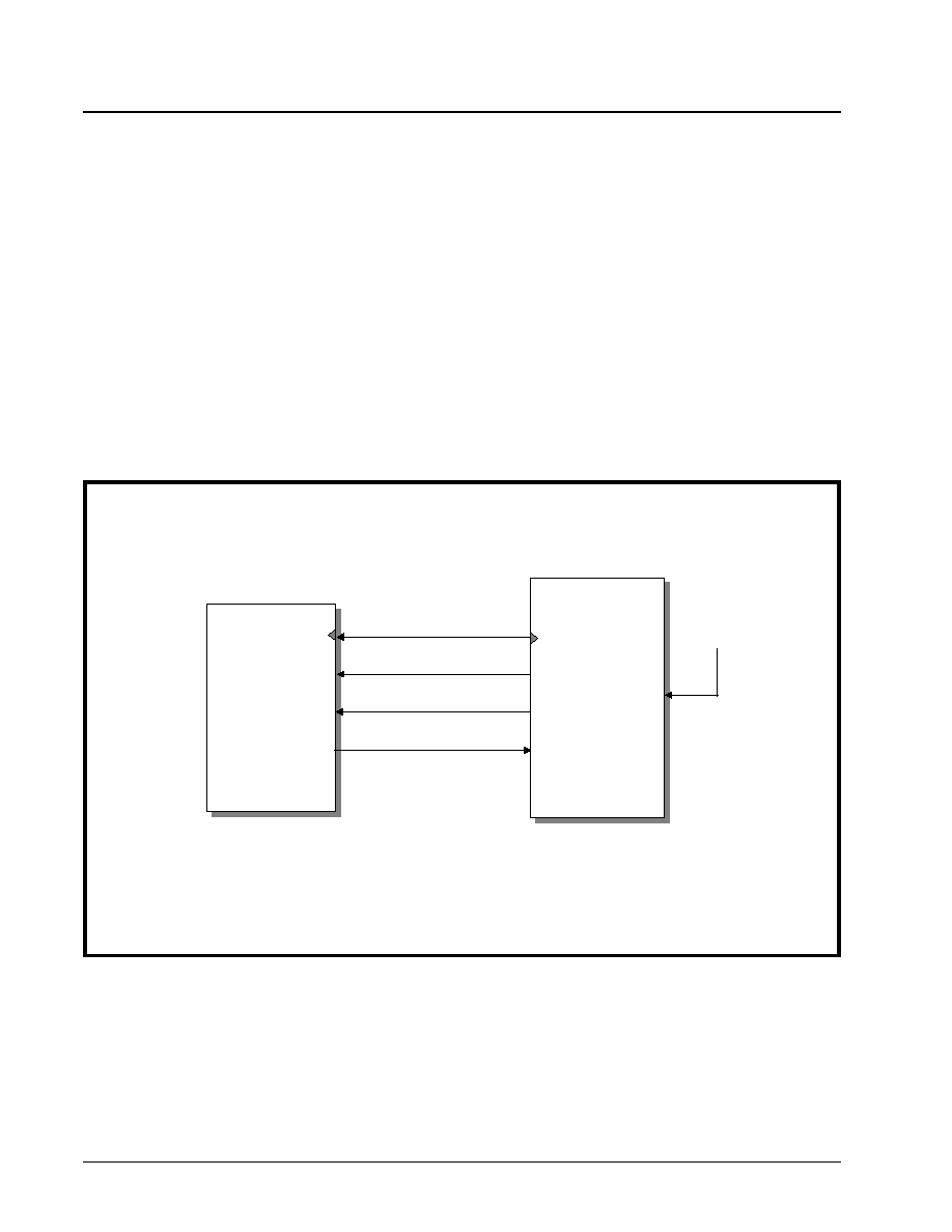
XRT7250
DS3/E3 FRAMER IC
·Á
·Á
·Á
·Á
REV. 1.1.1
218
Operation of the Receive Payload Data Output In-
terface block
The Receive Payload Data Output Interface permits
the user to read out the payload data of inbound DS3
frames, via either of the following modes.
∑ Serial Mode
∑ Nibble-Parallel Mode
Each of these modes are described in detail, below.
4.3.5.1
Serial Mode Operation
Behavior of the XRT7250
If the XRT7250 has been configured to operate in the
Serial mode, then the XRT7250 will behave as fol-
lows.
Payload Data Output
The XRT7250 will output the payload data, of the in-
coming DS3 frames via the RxSer output, upon the
rising edge of RxClk.
Delineation of inbound DS3 Frames
The XRT7250 will pulse the RxFrame output pin
"High" for one bit-period, coincident with it driving the
first bit within a given DS3 frame, via the RxSer out-
put pin.
Interfacing the XRT7250 to the Receive Terminal
Equipment
Figure 93 presents a simple illustration as how the
user should interface the XRT7250 to that terminal
equipment which processes Receive Direction pay-
load data.
Required Operation of the Terminal Equipment
The XRT7250 will update the data on the RxSer out-
put pin, upon the rising edge of RxClk. However, be-
cause the rising edge of RxClk to data delay is be-
tween 14ns to 16ns, the Terminal Equipment should
sample the data on the RxSer output pin (or the
DS3_Data_In pin at the Terminal Equipment) upon
the rising edge of RxClk. This will still permit the Ter-
minal Equipment with a RxSer to RxClk set-up time of
approximately 6ns and a hold time of 14 to 16ns. As
the Terminal Equipment samples RxSer with each ris-
ing edge of RxClk it should also be sampling the fol-
lowing signals.
∑ RxFrame
∑ RxOHInd
The Need for sampling RxFrame
F
IGURE
93. I
LLUSTRATION
OF
THE
XRT7250 DS3/E3 F
RAMER
IC
BEING
INTERFACED
TO
THE
R
ECEIVE
T
ERMINAL
E
QUIPMENT
(S
ERIAL
M
ODE
O
PERATION
)
Terminal Equipment
(Receive Payload Section)
XRT7250 DS3 Framer
DS3_Data_In
Rx_DS3_Clock_In
Rx_Start_of_Frame
RxClk
RxFrame
RxOHIns
44.736 MHz Clock Signal
RxSer
Rx_DS3_OH_Ind
RxLineClk
44.736 MHz
Clock Source

·Á
·Á
·Á
·Á
DS3/E3 FRAMER IC
XRT7250
REV. 1.1.1
219
The XRT7250 will pulse the RxFrame output pin
"High" coincident with it driving the very first bit of a
given DS3 frame onto the RxSer output pin. If knowl-
edge of the DS3 Frame Boundaries is important for
the operation of the Terminal Equipment, then this is
a very important signal for it to sample.
The Need for sampling RxOHInd
The XRT7250 will indicate that it is currently driving
an overhead bit onto the RxSer output pin, by pulsing
the RxOHInd output pin "High". If the Terminal Equip-
ment samples this signal "High", then it should know
that the bit, that it is currently sampling via the RxSer
pin is an overhead bit and should not be processed.
The Behavior of the Signals between the Receive
Payload Data Output Interface block and the Ter-
minal Equipment
The behavior of the signals between the XRT7250
and the Terminal Equipment for DS3 Serial Mode Op-
eration is illustrated in Figure 94.
4.3.5.2
Nibble-Parallel Mode Operation
Behavior of the XRT7250
If the XRT7250 has been configured to operate in the
Nibble-Parallel Mode, then the XRT7250 will behave
as follows.
Payload Data Output
The XRT7250 will output the payload data of the in-
coming DS3 frames, via the RxNib[3:0] output pins,
upon the falling edge of RxClk.
N
OTES
:
1. In this case, RxClk will function as the Nibble Clock
signal between the XRT7250 the Terminal Equip-
ment. The XRT7250 will pulse the RxClk output
signal "High" 1176 times, for each inbound DS3
frame.
2. Unlike Serial Mode operation, the duty cycle of
RxClk, in Nibble-Parallel Mode operation is approx-
imately 25%.
Delineation of Inbound DS3 Frames
The XRT7250 will pulse the RxFrame output pin
"High" for one nibble-period coincident with it driving
F
IGURE
94. A
N
I
LLUSTRATION
OF
THE
BEHAVIOR
OF
THE
SIGNALS
BETWEEN
THE
R
ECEIVE
P
AYLOAD
D
ATA
O
UTPUT
I
NTERFACE
BLOCK
OF
THE
XRT7250
AND
THE
T
ERMINAL
E
QUIPMENT
(S
ERIAL
M
ODE
O
PERATION
)
Terminal Equipment Signals
DS3_Clock_In
DS3_Data_In
Rx_Start_of_Frame
DS3_Overhead_Ind
XRT7250 Receive Payload Data I/F Signals
RxClk
RxSer
RxFrame
RxOH_Ind
Payload[4702]
Payload[4703]
X-Bit
Payload[0]
Payload[4702]
Payload[4703]
X-Bit
Payload[0]
Note: X-Bit will not be processed by the
Transmit Payload Data Input Interface.
DS3 Frame Number N
DS3 Frame Number N + 1
Note: RxFrame pulses high to denote
DS3 Frame Boundary.
Note: RxOH_Ind pulses high to
denote Overhead Data
(e.g., the X-bit).
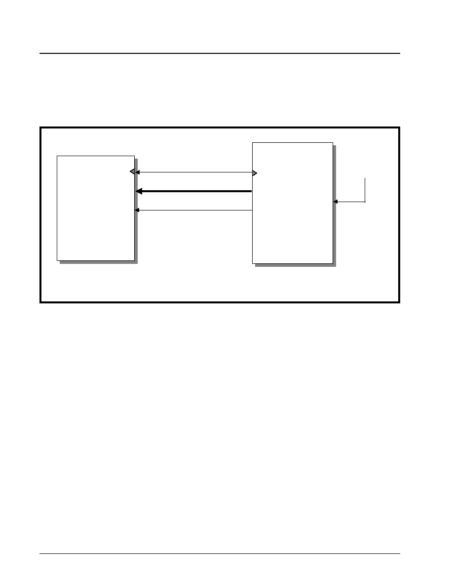
XRT7250
DS3/E3 FRAMER IC
·Á
·Á
·Á
·Á
REV. 1.1.1
220
the very first nibble, within a given inbound DS3
frame, via the RxNib[3:0] output pins.
Interfacing the XRT7250 the Terminal Equipment.
Figure 95 presents a simple illustration as how the
user should interface the XRT7250 to that terminal
equipment which processes Receive Direction pay-
load data.
Required Operation of the Terminal Equipment
The XRT7250 will update the data on the RxNib[3:0]
line, upon the falling edge of RxClk. Hence, the Ter-
minal Equipment should sample the data on the Rx-
Nib[3:0] output pins (or the DS3_Data_In[3:0] input
pins at the Terminal Equipment) upon the rising edge
of RxClk. As the Terminal Equipment samples RxSer
with each rising edge of RxClk it should also be sam-
pling the RxFrame signal.
The Need for Sampling RxFrame
The XRT7250 will pulse the RxFrame output pin
"High" coincident with it driving the very first nibble of
a given DS3 frame, onto the RxNib[3:0] output pins.
If knowledge of the DS3 Frame Boundaries is impor-
tant for the operation of the Terminal Equipment, then
this is a very important signal for it to sample.
N
OTE
: For DS3/Nibble-Parallel Mode Operation, none of
the Overhead bits will be output via the RxNib[3:0] output
pins. Hence, the RxOH_Ind output pin will be in-active in
this mode.
The Behavior of the Signals between the Receive
Payload Data Output Interface block and the Ter-
minal Equipment
The behavior of the signals between the XRT7250
and the Terminal Equipment for DS3 Nibble-Mode op-
eration is illustrated in Figure 96.
F
IGURE
95. I
LLUSTRATION
OF
THE
XRT7250 DS3/E3 F
RAMER
IC
BEING
INTERFACED
TO
THE
R
ECEIVE
S
ECTION
OF
THE
T
ERMINAL
E
QUIPMENT
(N
IBBLE
-M
ODE
O
PERATION
)
Terminal Equipment
(Receive Payload Section)
XRT7250 DS3 Framer
DS3_Data_In[3:0]
Rx_DS3_Clock_In
Rx_Start_of_Frame
RxClk
RxFrame
11.184 MHz Clock Signal
RxNib[3:0]
RxLineClk
44.736 MHz
Clock Source
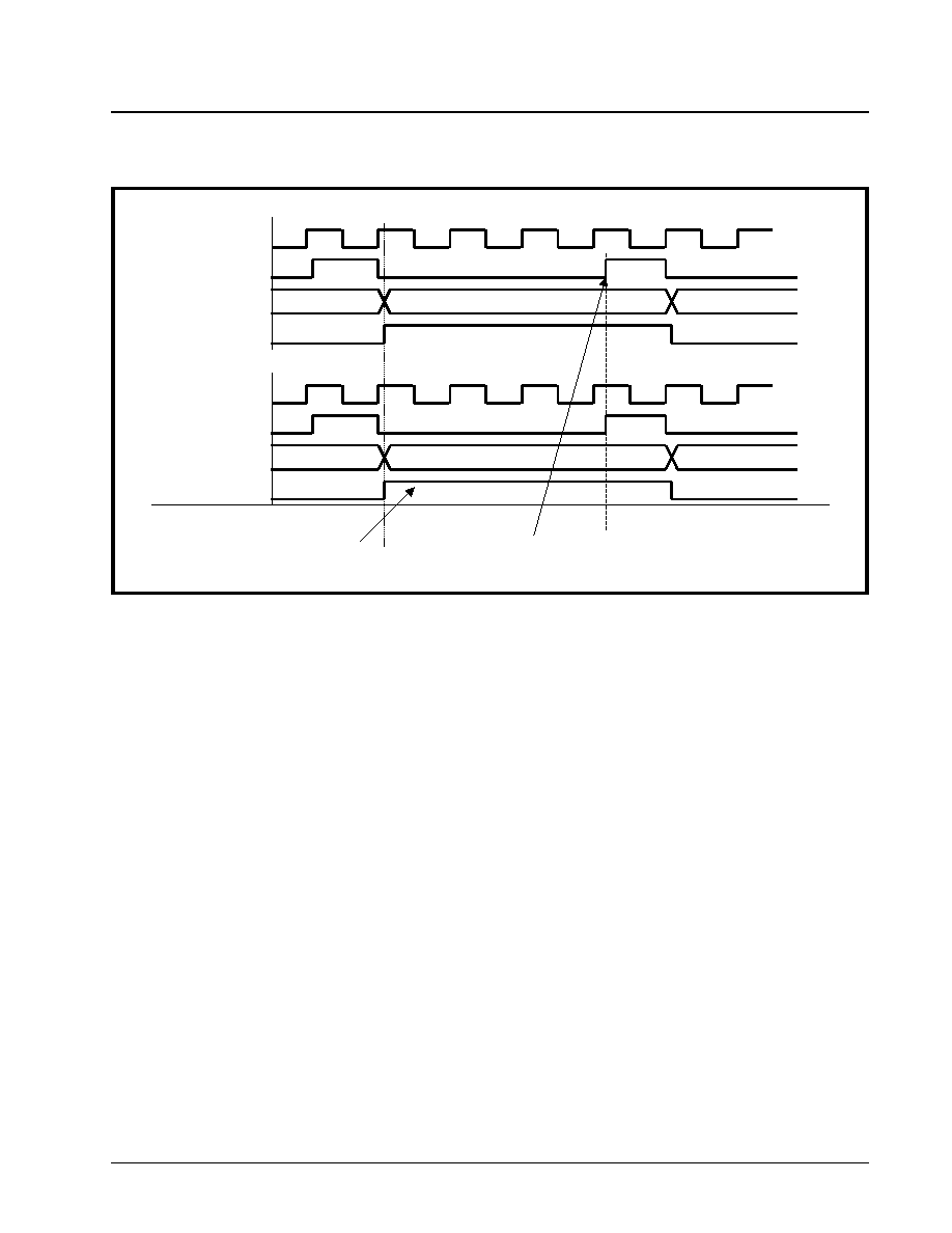
·Á
·Á
·Á
·Á
DS3/E3 FRAMER IC
XRT7250
REV. 1.1.1
221
4.3.6
Receive Section Interrupt Processing
The Receive Section of the XRT7250 can generate
an interrupt to the Microcontroller/Microprocessor for
the following reasons.
∑ Change of State of Receive LOS (Loss of Signal)
condition
∑ Change of State of Receive OOF (Out of Frame)
condition
∑ Change of State of Receive AIS (Alarm Indicator
Signal) condition
∑ Change of State of Receive Idle Condition.
∑ Change of State of Receive FERF (Far-End
Receive Failure) condition.
∑ Change of State of AIC (Application Identification
Channel) bit.
∑ Detection of P-Bit Error in a DS3 frame
∑ Detection of CP-Bit Error in a DS3 frame
∑ The Receive FEAC Message - Validation Interrupt
∑ The Receive FEAC Message - Removal Interrupt
∑ Completion of Reception of a LAPD Message
4.3.6.1
Enabling Receive Section Interrupts
As mentioned in Section 1.6, the Interrupt Structure,
within the XRT7250 contains two hierarchical levels.
∑ Block Level
∑ Source Level
The Block Level
The Enable state of the Block level for the Receive
Section Interrupts dictates whether or not interrupts
(if enabled at the source level), are actually enabled.
The user can enable or disable these Receive Sec-
tion interrupts, at the Block Level by writing the appro-
priate data into Bit 7 (Rx DS3/E3 Interrupt Enable)
within the Block Interrupt Enable register (Address =
0x04), as illustrated below.
F
IGURE
96. A
N
I
LLUSTRATION
OF
THE
B
EHAVIOR
OF
THE
SIGNALS
BETWEEN
THE
R
ECEIVE
P
AYLOAD
D
ATA
O
UTPUT
I
NTERFACE
B
LOCK
OF
THE
XRT7250
AND
THE
T
ERMINAL
E
QUIPMENT
(N
IBBLE
-M
ODE
O
PERATION
).
Terminal Equipment Signals
XRT7250 Receive Payload Data I/F Signals
DS3 Frame Number N
DS3 Frame Number N + 1
Note: RxFrame pulses high to denote
DS3 Frame Boundary.
RxOutClk
Rx_Start_of_Frame
Rx_DS3_Clock_In
DS3_Data_In[3:0]
Nibble [0]
Nibble [1]
RxOutClk
RxFrame
RxClk
RxNib[3:0]
Nibble [0]
Nibble [1]
Recommended Sampling Edge of Terminal
Equipment
XRT7250
DS3/E3 FRAMER IC
·Á
·Á
·Á
·Á
REV. 1.1.1
222
Setting this bit-field to "1" enables the Receive Sec-
tion (at the Block Level) for interrupt generation. Con-
versely, setting this bit-field to "0" disables the Re-
ceive Section for interrupt generation.
4.3.6.2
Enabling/Disabling and Servicing
Receive Section Interrupts
As mentioned earlier, the Receive Section of the
XRT7250 Framer IC contains numerous interrupts.
The Enabling/Disabling and Servicing of each of
these interrupts is described below.
4.3.6.2.1
The Change of State on Receive LOS
Interrupt
If the Change of State on Receive LOS (Loss of Sig-
nal) Interrupt is enabled, then the XRT7250 Framer
IC will generate an interrupt in response to either of
the following conditions.
1. When the XRT7250 Framer IC declares an LOS
(Loss of Signal) condition, and
2. When the XRT7250 Framer IC clears the LOS
(Loss of Signal) condition.
Conditions causing the XRT7250 Framer IC to de-
clare an LOS condition
∑ If the XRT7300 LIU IC declares an LOS condition,
and drives the RLOS input pin (of the XRT7250
Framer IC) "High".
∑ If the XRT7250 Framer IC detects a 180 consecu-
tive "0's", via the RxPOS and RxNEG input pins.
Conditions causing the XRT7250 Framer IC to
clear the LOS condition.
∑ When the XRT7300 LIU IC ceases declaring an
LOS condition and drives the RLOS input pin (of
the XRT7250 Framer IC) "Low".
∑ When the XRT7250 Framer IC detects at least 60
marks (via the RxPOS and RxNEG input pins) out
of 180 bit-periods.
Enabling and Disabling the Change of State on
Receive LOS Interrupt:
The user can enable or disable the Change of State
on Receive LOS Interrupt, by writing the appropriate
value into Bit 6 (LOS Interrupt Enable) within the
RxDS3 Interrupt Enable Register, as illustrated below.
Setting this bit-field to "1" enables this interrupt. Con-
versely, setting this bit-field to "0" disables this inter-
rupt.
Servicing the Change of State on Receive LOS In-
terrupt
Whenever the XRT7250 Framer IC detects this inter-
rupt, it will do all of the following.
∑ It will assert the Interrupt Request output pin (INT)
by driving this pin "Low".
BLOCK INTERRUPT ENABLE REGISTER (ADDRESS = 0X04)
B
IT
7
B
IT
6
B
IT
5
B
IT
4
B
IT
3
B
IT
2
B
IT
1
B
IT
0
RxDS3/E3
Interrupt
Enable
Not Used
TxDS3/E3
Interrupt
Enable
One Second
Interrupt
Enable
R/W
RO
RO
RO
RO
RO
R/W
R/W
X
0
0
0
0
0
0
0
RXDS3 INTERRUPT ENABLE REGISTER (ADDRESS = 0X12)
B
IT
7
B
IT
6
B
IT
5
B
IT
4
B
IT
3
B
IT
2
B
IT
1
B
IT
0
CP Bit Error
Interrupt
Enable
LOS
Interrupt
Enable
AIS
Interrupt
Enable
Idle Interrupt
Enable
FERF
Interrupt
Enable
AIC
Interrupt
Enable
OOF
Interrupt
Enable
P-Bit Error
Interrupt
Enable
R/W
R/W
R/W
R/W
R/W
R/W
R/W
R/W
0
0
0
0
0
0
0
0

·Á
·Á
·Á
·Á
DS3/E3 FRAMER IC
XRT7250
REV. 1.1.1
223
∑ It will set Bit 6 (LOS Interrupt Status) within the
RxDS3 Interrupt Status register to "1", as illustrated
below.
Whenever the user's system encounters the Change
of LOS on Receive Interrupt, then it should do the fol-
lowing.
1. It should determine the current state of the LOS
condition. Recall, that this interrupt can gener-
ated, whenever the XRT7250 Framer declares or
clears the LOS defects. Hence, the user can
determine the current state of the LOS defect by
reading the state of Bit 6 (RxLOS), within the
RxDS3 Configuration & Status Registers, as illus-
trated below.
If the LOS State is TRUE
1. It should transmit a FERF (Far-End Receive Fail-
ure) to the Remote Terminal Equipment. The
XRT7250 Framer IC automatically supports this
action via the FERF-upon-LOS feature.
2. It should transmit the appropriate FEAC Message
(per Bellcore GR-499-CORE), to the Remote Ter-
minal, indicating that a Loss of Signal condition
has been declared.
If the LOS State is FALSE
1. It should cease transmitting a FERF indicator to
the Remote Terminal Equipment. The XRT7250
Framer IC automatically supports this action via
the FERF-upon-LOS feature.
2. It should transmit the appropriate FEAC Message
(per Bellcore GR-499-CORE), to the Remote Ter-
minal Equipment, indicating that the Loss of Sig-
nal condition has been cleared.
4.3.6.2.2
The Change of State on Receive OOF
Interrupt
If the Change of State on Receive OOF (Out-of-
Frame) Interrupt is enabled, then the XRT7250 Fram-
er IC will generate an interrupt in response to either of
the following conditions.
1. When the XRT7250 Framer IC declares an OOF
(Out of Frame) condition, and
2. When the XRT7250 Framer IC clears the OOF
(Out of Frame) condition.
Conditions causing the XRT7250 Framer IC to de-
clare an OOF condition
∑ If the Receive DS3 Framer block (within the
XRT7250 Framer IC) detects at least either 3 or 6
F-bit errors, in the last 16 F-bits.
Conditions causing the XRT7250 Framer IC to
clear the OOF condition.
∑ Whenever, the Receive DS3 Framer block transi-
tions from the M-Bit Search into the In-Frame state
(within the Frame Acquisition/Maintenance State
Machine Diagram).
Enabling and Disabling the Change of State on
Receive OOF Interrupt:
The user can enable or disable the Change of State
on Receive OOF Interrupt, by writing the appropriate
RXDS3 INTERRUPT STATUS REGISTER (ADDRESS = 0X13)
B
IT
7
B
IT
6
B
IT
5
B
IT
4
B
IT
3
B
IT
2
B
IT
1
B
IT
0
CP-Bit Error
Interrupt
Status
LOS
Interrupt
Status
AIS
Interrupt
Status
Idle Interrupt
Status
FERF
Interrupt
Status
AIC
Interrupt
Status
OOF
Interrupt
Status
P-Bit Error
Interrupt
Status
RUR
RUR
RUR
RUR
RUR
RUR
RUR
RUR
0
1
0
0
0
0
0
0
RXDS3 CONFIGURATION & STATUS REGISTER (ADDRESS = 0X10)
B
IT
7
B
IT
6
B
IT
5
B
IT
4
B
IT
3
B
IT
2
B
IT
1
B
IT
0
RxAIS
RxLOS
RxIdle
RxOOF
Reserved
Framing On
Parity
FSync
Algo
MSync
Algo
RO
RO
RO
RO
RO
RO
RO
RUR
0
1
0
0
0
0
0
0

XRT7250
DS3/E3 FRAMER IC
·Á
·Á
·Á
·Á
REV. 1.1.1
224
value into Bit 1 (OOF Interrupt Enable) within the
RxDS3 Interrupt Enable Register, as illustrated below.
Setting this bit-field to "1" enables this interrupt. Con-
versely, setting this bit-field to "0" disables this inter-
rupt.
Servicing the Change of State on Receive OOF In-
terrupt
Whenever the XRT7250 Framer IC detects this inter-
rupt, it will do all of the following.
∑ It will assert the Interrupt Request output pin (INT)
by driving this pin "Low".
∑ It will set Bit 1 (OOF Interrupt Status), within the
RxDS3 Interrupt Status Register to "1", as indicated
below.
Whenever the Terminal Equipment encounters a
Change in OOF on Receive Interrupt, then it should
do the following.
1. It should determine the current state of the OOF
condition. Recall, that this interrupt can gener-
ated, whenever the XRT7250 Framer declares or
clears the OOF defects. Hence, the user can
determine the current state of the OOF defect by
reading the state of Bit 4 (RxOOF), within the
RxDS3 Configuration & Status Registers, as illus-
trated below.
If OOF is TRUE.
1. It should transmit a FERF (Far-End Receive Fail-
ure) to the Remote Terminal Equipment. The
XRT7250 Framer IC automatically supports this
action via the FERF-upon-OOF feature.
2. It should transmit the appropriate FEAC Message
(per Bellcore GR-499-CORE), to the Remote Ter-
minal, indicating that a Service Affecting condi-
tion has been detected in the Local Terminal
Equipment.
if OOF is FALSE
1. It should cease transmitting a FERF (Far-End
Receive Failure) indicator to the Remote Terminal
Equipment. The XRT7250 Framer IC automati-
cally supports this action via the FERF-upon-
OOF feature.
RXDS3 INTERRUPT ENABLE REGISTER (ADDRESS = 0X12)
B
IT
7
B
IT
6
B
IT
5
B
IT
4
B
IT
3
B
IT
2
B
IT
1
B
IT
0
CP Bit Error
Interrupt
Enable
LOS
Interrupt
Enable
AIS
Interrupt
Enable
Idle Interrupt
Enable
FERF
Interrupt
Enable
AIC
Interrupt
Enable
OOF
Interrupt
Enable
P-Bit Error
Interrupt
Enable
R/W
R/W
R/W
R/W
R/W
R/W
R/W
R/W
0
0
0
0
0
0
0
0
RXDS3 INTERRUPT STATUS REGISTER (ADDRESS = 0X13)
B
IT
7
B
IT
6
B
IT
5
B
IT
4
B
IT
3
B
IT
2
B
IT
1
B
IT
0
CP-Bit Error
Interrupt
Status
LOS
Interrupt
Status
AIS
Interrupt
Status
Idle Interrupt
Status
FERF
Interrupt
Status
AIC
Interrupt
Status
OOF
Interrupt
Status
P-Bit Error
Interrupt
Status
RUR
RUR
RUR
RUR
RUR
RUR
RUR
RUR
0
0
0
0
0
0
1
0
RXDS3 CONFIGURATION & STATUS REGISTER (ADDRESS = 0X10)
B
IT
7
B
IT
6
B
IT
5
B
IT
4
B
IT
3
B
IT
2
B
IT
1
B
IT
0
RxAIS
RxLOS
RxIdle
RxOOF
Reserved
Framing On
Parity
FSync
Algo
MSync
Algo
RO
RO
RO
RO
RO
RO
RO
RUR
0
0
0
0
0
0
0
0

·Á
·Á
·Á
·Á
DS3/E3 FRAMER IC
XRT7250
REV. 1.1.1
225
2. It should transmit the appropriate FEAC Message
(per Bellcore GR-499-CORE), to the Remote Ter-
minal Equipment, indicating that the Service
Affecting condition has been cleared.
4.3.6.2.3
The Change of State of Receive AIS
Interrupt
If the Change of State on Receive AIS (Alarm Indica-
tion Signal) Interrupt is enabled, then the XRT7250
Framer IC will generate an interrupt in response to ei-
ther of the following conditions.
1. When the XRT7250 Framer IC detects an AIS
pattern, in the incoming DS3 data stream, and
2. When the XRT7250 Framer IC no longer detects
the AIS pattern in the incoming DS3 data stream.
Conditions causing the XRT7250 Framer IC to de-
clare an AIS condition
∑ If the Receive DS3 Framer block (within the
XRT7250 Framer IC) detects at least 63 DS3
frames, which contains the AIS pattern.
Conditions causing the XRT7250 Framer IC to
clear the AIS condition.
∑ Whenever, the Receive DS3 Framer block detects
63 DS3 frames, which do not contain the AIS pat-
tern.
Enabling and Disabling the Change of State on
Receive AIS Interrupt:
The user can enable or disable the Change of State
on Receive AIS Interrupt, by writing the appropriate
value into Bit 5 (AIS Interrupt Enable) within the
RxDS3 Interrupt Enable Register, as illustrated below.
Setting this bit-field to "1" enables this interrupt. Con-
versely, setting this bit-field to "0" disables this inter-
rupt.
Servicing the Change of State on Receive AIS In-
terrupt
Whenever the XRT7250 Framer IC detects this inter-
rupt, it will do all of the following.
∑ It will assert the Interrupt Request output pin (INT)
by driving it "Low".
∑ It will set Bit 5 (AIS Interrupt Status) within the
RxDS3 Interrupt Status Register, to "1", as indi-
cated below.
Whenever the Terminal Equipment encounters a
Change in AIS on Receive interrupt, it should do the
following.
1. It should determine the current state of the AIS
condition. Recall, that this interrupt can gener-
ated, whenever the XRT7250 Framer declares or
clears the AIS defects. Hence, the user can
determine the current state of the AIS defect by
reading the state of Bit 7 (RxAIS), within the
RxDS3 Configuration & Status Registers, as illus-
trated below
RXDS3 INTERRUPT ENABLE REGISTER (ADDRESS = 0X12)
B
IT
7
B
IT
6
B
IT
5
B
IT
4
B
IT
3
B
IT
2
B
IT
1
B
IT
0
CP Bit Error
Interrupt
Enable
LOS
Interrupt
Enable
AIS
Interrupt
Enable
Idle Interrupt
Enable
FERF
Interrupt
Enable
AIC
Interrupt
Enable
OOF
Interrupt
Enable
P-Bit Error
Interrupt
Enable
R/W
R/W
R/W
R/W
R/W
R/W
R/W
R/W
0
0
0
0
0
0
0
0
RXDS3 INTERRUPT STATUS REGISTER (ADDRESS = 0X13)
B
IT
7
B
IT
6
B
IT
5
B
IT
4
B
IT
3
B
IT
2
B
IT
1
B
IT
0
CP-Bit Error
Interrupt
Status
LOS
Interrupt
Status
AIS
Interrupt
Status
Idle Interrupt
Status
FERF
Interrupt
Status
AIC
Interrupt
Status
OOF
Interrupt
Status
P-Bit Error
Interrupt
Status
RUR
RUR
RUR
RUR
RUR
RUR
RUR
RUR
0
0
1
0
0
0
0
0
XRT7250
DS3/E3 FRAMER IC
·Á
·Á
·Á
·Á
REV. 1.1.1
226
If the AIS Condition is TRUE
1. The Local Terminal Equipment should transmit a
FERF (Far-End Receive Failure) to the Remote
Terminal Equipment. The XRT7250 Framer IC
automatically supports this action via the FERF-
upon-AIS feature.
2. It should transmit the appropriate FEAC Message
(per Bellcore GR-499-CORE), to the Remote Ter-
minal, indicating that a Service Affecting condi-
tion has been detected in the Local Terminal
Equipment.
If the AIS Condition is FALSE
1. The Local Terminal Equipment should cease
transmitting a FERF (Far-End Receive Failure)
indicator to the Remote Terminal Equipment.
The XRT7250 Framer IC automatically supports
this action via the FERF-upon-AIS feature.
2. It should transmit the appropriate FEAC Message
(per Bellcore GR-499-CORE) to the Remote Ter-
minal, indicates that the Service Affecting condi-
tion no longer exists.
4.3.6.2.4
The Change of State of Receive Idle
Interrupt
If the Change of State on Receive Idle Interrupt is en-
abled, then the XRT7250 Framer IC will generate an
interrupt in response to either of the following condi-
tions.
1. When the XRT7250 Framer IC detects an Idle
pattern, in the incoming DS3 data stream, and
2. When the XRT7250 Framer IC no longer detects
the Idle pattern in the incoming DS3 data stream.
Conditions causing the XRT7250 Framer IC to de-
clare an Idle condition
∑ If the Receive DS3 Framer block (within the
XRT7250 Framer IC) detects at least 63 DS3
frames, which contains the Idle pattern.
Conditions causing the XRT7250 Framer IC to
clear the Idle condition.
∑ Whenever, the Receive DS3 Framer block detects
63 DS3 frames, which do not contain the Idle pat-
tern.
Enabling and Disabling the Change of State on
Receive Idle Interrupt:
The user can enable or disable the Change of State
on Receive Idle Interrupt, by writing the appropriate
value into Bit 4 (Idle Interrupt Enable) within the
RxDS3 Interrupt Enable Register, as illustrated below.
Setting this bit-field to "1" enables this interrupt. Con-
versely, setting this bit-field to "0" disables this inter-
rupt.
Servicing the Change of State on Receive Idle In-
terrupt
Whenever the XRT7250 Framer IC detects this inter-
rupt, it will do all of the following.
∑ It will assert the Interrupt Request Output pin (INT)
by driving it "Low".
∑ It will set Bit 4 (Idle Interrupt Status), within the Rx
DS3 Interrupt Status Register to "1", as indicated
below.
RXDS3 CONFIGURATION & STATUS REGISTER (ADDRESS = 0X10)
B
IT
7
B
IT
6
B
IT
5
B
IT
4
B
IT
3
B
IT
2
B
IT
1
B
IT
0
RxAIS
RxLOS
RxIdle
RxOOF
Reserved
Framing On
Parity
FSync
Algo
MSync
Algo
RO
RO
RO
RO
RO
RO
RO
RUR
0
0
0
0
0
0
0
0
RXDS3 INTERRUPT ENABLE REGISTER (ADDRESS = 0X12)
B
IT
7
B
IT
6
B
IT
5
B
IT
4
B
IT
3
B
IT
2
B
IT
1
B
IT
0
CP Bit Error
Interrupt
Enable
LOS
Interrupt
Enable
AIS
Interrupt
Enable
Idle Interrupt
Enable
FERF
Interrupt
Enable
AIC
Interrupt
Enable
OOF
Interrupt
Enable
P-Bit Error
Interrupt
Enable
R/W
R/W
R/W
R/W
R/W
R/W
R/W
R/W
0
0
0
0
0
0
0
0

·Á
·Á
·Á
·Á
DS3/E3 FRAMER IC
XRT7250
REV. 1.1.1
227
Whenever the Terminal Equipment encounters the
Change in Idle Condition Receive Interrupt, it should
do the following.
1. It should determine the current state of the Idle
condition. Recall, that this interrupt can gener-
ated, whenever the XRT7250 Framer declares or
clears the Idle condition. Hence, the user can
determine the current state of the Idle condition
by reading the state of Bit 5 (RxIdle), within the
RxDS3 Configuration & Status Registers, as illus-
trated below
4.3.6.2.5
The Change of State of Receive FERF
Interrupt
If the Change of State on Receive FERF Interrupt is
enabled, then the XRT7250 Framer IC will generate
an interrupt in response to either of the following con-
ditions.
1. When the XRT7250 Framer IC detects the FERF
indicator, in the incoming DS3 data stream, and
2. When the XRT7250 Framer IC no longer detects
the FERF indicator, in the incoming DS3 data
stream.
Conditions causing the XRT7250 Framer IC to de-
clare an FERF (Far-End-Receive Failure) condi-
tion
∑ If the Receive DS3 Framer block (within the
XRT7250 Framer IC) detects some incoming DS3
frames with both of the "X" bits set to "0".
Conditions causing the XRT7250 Framer IC to
clear the FERF condition.
∑ Whenever, the Receive DS3 Framer block starts to
detect some incoming DS3 frames, in which the "X"
bits are not set to "0".
Enabling and Disabling the Change of State on
Receive FERF Interrupt:
The user can enable or disable the Change of State
on Receive FERF Interrupt, by writing the appropriate
value into Bit 3 (FERF Interrupt Enable) within the
RxDS3 Interrupt Enable Register, as illustrated below.
Setting this bit-field to "1" enables this interrupt. Con-
versely, setting this bit-field to "0" disables this inter-
rupt.
Servicing the Change of State on Receive FERF
Interrupt
RXDS3 INTERRUPT STATUS REGISTER (ADDRESS = 0X13)
B
IT
7
B
IT
6
B
IT
5
B
IT
4
B
IT
3
B
IT
2
B
IT
1
B
IT
0
CP-Bit Error
Interrupt
Status
LOS
Interrupt
Status
AIS
Interrupt
Status
Idle Interrupt
Status
FERF
Interrupt
Status
AIC
Interrupt
Status
OOF
Interrupt
Status
P-Bit Error
Interrupt
Status
RUR
RUR
RUR
RUR
RUR
RUR
RUR
RUR
0
0
0
1
0
0
0
0
RXDS3 CONFIGURATION & STATUS REGISTER (ADDRESS = 0X10)
B
IT
7
B
IT
6
B
IT
5
B
IT
4
B
IT
3
B
IT
2
B
IT
1
B
IT
0
RxAIS
RxLOS
RxIdle
RxOOF
Reserved
Framing On
Parity
FSync
Algo
MSync
Algo
RO
RO
RO
RO
RO
RO
RO
RUR
0
0
0
0
0
0
0
0
RXDS3 INTERRUPT ENABLE REGISTER (ADDRESS = 0X12)
B
IT
7
B
IT
6
B
IT
5
B
IT
4
B
IT
3
B
IT
2
B
IT
1
B
IT
0
CP Bit Error
Interrupt
Enable
LOS
Interrupt
Enable
AIS
Interrupt
Enable
Idle Interrupt
Enable
FERF
Interrupt
Enable
AIC
Interrupt
Enable
OOF
Interrupt
Enable
P-Bit Error
Interrupt
Enable
R/W
R/W
R/W
R/W
R/W
R/W
R/W
R/W
0
0
0
0
0
0
0
0
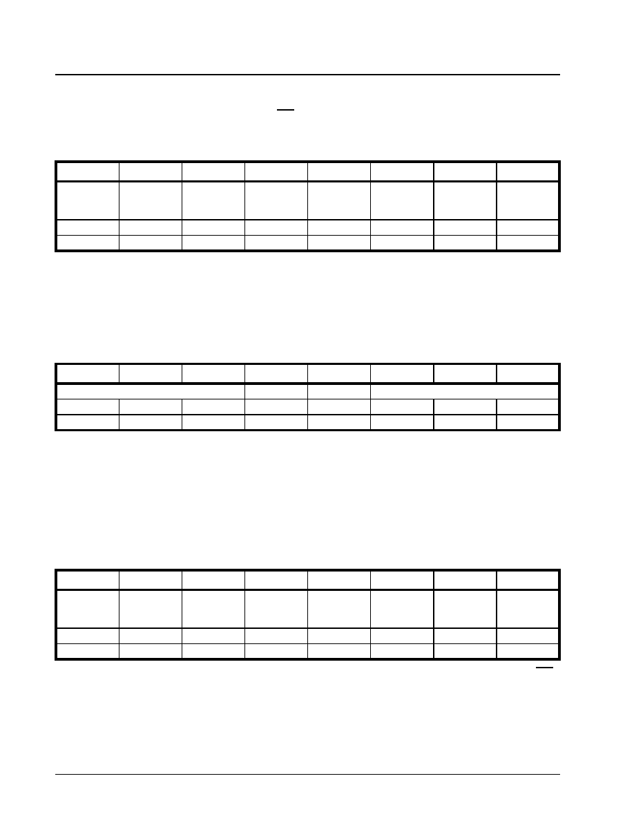
XRT7250
DS3/E3 FRAMER IC
·Á
·Á
·Á
·Á
REV. 1.1.1
228
Whenever the XRT7250 Framer IC detects this inter-
rupt, it will do all of the following.
∑ It will assert the Interrupt Request Output pin (INT)
by driving it "High".
∑ It will set Bit 3 (FERF Interrupt Status), within the
Rx DS3 Interrupt Status Register, to "1", as indi-
cated below.
Whenever the Terminal Equipment encounters a
Change in FERF Condition on Receive Interrupt, it
should do the following.
1. It should determine the current state of the FERF
condition. Recall, that this interrupt can gener-
ated, whenever the XRT7250 Framer declares or
clears the FERF condition. Hence, the user can
determine the current state of the FERF condition
by reading the state of Bit 5 (RxIdle), within the
RxDS3 Configuration & Status Registers, as illus-
trated below
4.3.6.2.6
The Change of State of Receive AIC
Interrupt
If the Change of State of Receive AIC Interrupt is en-
abled, then the XRT7250 Framer IC will generate an
interrupt, anytime the Receive DS3 Framer block has
detected a change in the value of the AIC bit, within
the incoming DS3 data stream.
Enabling and Disabling the Change of State of
Receive AIC Interrupt:
The user can enable or disable the Change of State
on Receive AIC Interrupt, by writing the appropriate
value into Bit 2 (AIC Interrupt Enable) within the
RxDS3 Interrupt Enable Register, as illustrated below.
Setting this bit-field to "1" enables this interrupt. Con-
versely, setting this bit-field to "0" disables this inter-
rupt.
Servicing the Change of State on Receive AIC In-
terrupt
Whenever the XRT7250 Framer IC detects this inter-
rupt, it will do all of the following.
∑ It will assert the Interrupt Request Output pin (INT)
by driving it "High".
∑ It will set Bit 3 (AIC Interrupt Status), within the Rx
DS3 Interrupt Status Register, to "1", as indicated
below.
RXDS3 INTERRUPT STATUS REGISTER (ADDRESS = 0X13)
B
IT
7
B
IT
6
B
IT
5
B
IT
4
B
IT
3
B
IT
2
B
IT
1
B
IT
0
CP-Bit Error
Interrupt
Status
LOS
Interrupt
Status
AIS
Interrupt
Status
Idle Interrupt
Status
FERF
Interrupt
Status
AIC
Interrupt
Status
OOF
Interrupt
Status
P-Bit Error
Interrupt
Status
RUR
RUR
RUR
RUR
RUR
RUR
RUR
RUR
0
0
0
0
1
0
0
0
RXDS3 STATUS REGISTER (ADDRESS = 0X11)
B
IT
7
B
IT
6
B
IT
5
B
IT
4
B
IT
3
B
IT
2
B
IT
1
B
IT
0
Reserved
RxFERF
RxAIC
RxFEBE[2:0]
RO
RO
RO
RO
RO
RO
RO
RO
0
0
0
0
0
0
0
0
RXDS3 INTERRUPT ENABLE REGISTER (ADDRESS = 0X12)
B
IT
7
B
IT
6
B
IT
5
B
IT
4
B
IT
3
B
IT
2
B
IT
1
B
IT
0
CP Bit Error
Interrupt
Enable
LOS
Interrupt
Enable
AIS
Interrupt
Enable
Idle Interrupt
Enable
FERF
Interrupt
Enable
AIC
Interrupt
Enable
OOF
Interrupt
Enable
P-Bit Error
Interrupt
Enable
R/W
R/W
R/W
R/W
R/W
R/W
R/W
R/W
0
0
0
0
0
0
0
0
·Á
·Á
·Á
·Á
DS3/E3 FRAMER IC
XRT7250
REV. 1.1.1
229
Whenever the Terminal Equipment encounters this in-
terrupt, it should do the following.
∑ It should continue to check the state of the AIC bit,
in order to see if this change is constant.
∑ If this change is constant, then the user should con-
figure the XRT7250 Framer IC to operate in the
M13 framing format, if the AIC bit-field is "0".
∑ Conversely, if the AIC bit-field is "1", then the user
should configure the XRT7250 Framer IC to oper-
ate in the C-bit Parity framing format.
4.3.6.2.7
The Detection of P-Bit Error Interrupt
If the Detection of P-Bit Error Interrupt is enabled,
then the XRT7250 Framer IC will generate an inter-
rupt, anytime the Receive DS3 Framer block has de-
tected a P-bit error, within the incoming DS3 data
stream.
Enabling and Disabling the Detection of P-Bit Er-
ror Interrupt:
The user can enable or disable the Detection of P-Bit
Error Interrupt, by writing the appropriate value into
Bit 0 (P-Bit Error Interrupt Enable) within the RxDS3
Interrupt Enable Register, as illustrated below.
Setting this bit-field to "1" enables this interrupt. Con-
versely, setting this bit-field to "0" disables this inter-
rupt.
Servicing the Detection of P-Bit Error Interrupt
Whenever the XRT7250 Framer IC detects this inter-
rupt, it will do all of the following.
∑ It will assert the Interrupt Request output pin (INT)
by driving it "High".
∑ It will set Bit 0 (P-Bit Error Interrupt Status) within
the Rx DS3 Interrupt Status Register, to "1", as indi-
cated below.
Whenever the Terminal Equipment encounters the
Detection of P-bit Error Interrupt, It should read the
contents of PMON Parity Error Count Register (locat-
ed at 0x54 and 0x55), in order to determine the num-
ber of P-bit errors recently received.
RXDS3 INTERRUPT STATUS REGISTER (ADDRESS = 0X13)
B
IT
7
B
IT
6
B
IT
5
B
IT
4
B
IT
3
B
IT
2
B
IT
1
B
IT
0
CP-Bit Error
Interrupt
Status
LOS
Interrupt
Status
AIS
Interrupt
Status
Idle Interrupt
Status
FERF
Interrupt
Status
AIC
Interrupt
Status
OOF
Interrupt
Status
P-Bit Error
Interrupt
Status
RUR
RUR
RUR
RUR
RUR
RUR
RUR
RUR
0
0
0
0
0
1
0
0
RXDS3 INTERRUPT ENABLE REGISTER (ADDRESS = 0X12)
B
IT
7
B
IT
6
B
IT
5
B
IT
4
B
IT
3
B
IT
2
B
IT
1
B
IT
0
CP Bit Error
Interrupt
Enable
LOS
Interrupt
Enable
AIS
Interrupt
Enable
Idle Interrupt
Enable
FERF
Interrupt
Enable
AIC
Interrupt
Enable
OOF
Interrupt
Enable
P-Bit Error
Interrupt
Enable
R/W
R/W
R/W
R/W
R/W
R/W
R/W
R/W
0
0
0
0
0
0
0
0
RXDS3 INTERRUPT STATUS REGISTER (ADDRESS = 0X13)
B
IT
7
B
IT
6
B
IT
5
B
IT
4
B
IT
3
B
IT
2
B
IT
1
B
IT
0
CP-Bit Error
Interrupt
Status
LOS
Interrupt
Status
AIS
Interrupt
Status
Idle Interrupt
Status
FERF
Interrupt
Status
AIC
Interrupt
Status
OOF
Interrupt
Status
P-Bit Error
Interrupt
Status
RUR
RUR
RUR
RUR
RUR
RUR
RUR
RUR
0
0
0
0
0
0
0
1

XRT7250
DS3/E3 FRAMER IC
·Á
·Á
·Á
·Á
REV. 1.1.1
230
4.3.6.2.8
The Detection of CP-Bit Error Inter-
rupt
If the Detection of CP-Bit Error Interrupt is enabled,
then the XRT7250 Framer IC will generate an inter-
rupt, anytime the Receive DS3 Framer block has de-
tected a CP-bit error, within the incoming DS3 data
stream.
Enabling and Disabling the Detection of CP-Bit
Error Interrupt:
The user can enable or disable the Detection of CP-
Bit Error Interrupt, by writing the appropriate value in-
to Bit 7 (CP-Bit Error Interrupt Enable) within the
RxDS3 Interrupt Enable Register, as illustrated below.
Setting this bit-field to "1" enables this interrupt. Con-
versely, setting this bit-field to "0" disables this inter-
rupt.
Servicing the Detection of CP-Bit Error Interrupt
Whenever the XRT7250 Framer IC detects this inter-
rupt, it will do all of the following.
∑ It will assert the Interrupt Request output pin (INT)
by driving it "High".
∑ It will set Bit 7 (CP-Bit Error Interrupt Status) within
the Rx DS3 Interrupt Status Register, to "1", as indi-
cated below.
Whenever the Terminal Equipment encounters the
Detection of CP-bit Error Interrupt, it should do the
following.
∑ It should read contents of PMON Frame CP-Bit
Error Count Register (located at 0x72 and 0x73), in
order to determine the number of CP-bit errors
recently received.
4.3.6.2.9
The Receive FEAC Message - Valida-
tion Interrupt
If the Receive FEAC Message - Validation Interrupt is
enabled, then the XRT7250 Framer IC will generate
an interrupt any time the Receive FEAC Processor
validates a new FEAC (Far-End Alarm & Control)
Message.
In particular, the Receive FEAC Processor will vali-
date a FEAC Message, it that same FEAC Message
has been received in 8 of the last 10 FEAC Message
receptions.
Enabling/Disabling the Receive FEAC Message -
Validation Interrupt
The user can enable or disable the Receive FEAC
Message - Validation Interrupt, by writing the appro-
priate data into Bit 1 (RxFEAC Valid Interrupt Enable)
within the RxDS3 FEAC Interrupt Enable/Status Reg-
ister, as indicated below.
RXDS3 INTERRUPT ENABLE REGISTER (ADDRESS = 0X12)
B
IT
7
B
IT
6
B
IT
5
B
IT
4
B
IT
3
B
IT
2
B
IT
1
B
IT
0
CP Bit Error
Interrupt
Enable
LOS
Interrupt
Enable
AIS
Interrupt
Enable
Idle Interrupt
Enable
FERF
Interrupt
Enable
AIC
Interrupt
Enable
OOF
Interrupt
Enable
P-Bit Error
Interrupt
Enable
R/W
R/W
R/W
R/W
R/W
R/W
R/W
R/W
0
0
0
0
0
0
0
0
RXDS3 INTERRUPT STATUS REGISTER (ADDRESS = 0X13)
B
IT
7
B
IT
6
B
IT
5
B
IT
4
B
IT
3
B
IT
2
B
IT
1
B
IT
0
CP-Bit Error
Interrupt
Status
LOS
Interrupt
Status
AIS
Interrupt
Status
Idle Interrupt
Status
FERF
Interrupt
Status
AIC
Interrupt
Status
OOF
Interrupt
Status
P-Bit Error
Interrupt
Status
RUR
RUR
RUR
RUR
RUR
RUR
RUR
RUR
1
0
0
0
0
0
0
1
·Á
·Á
·Á
·Á
DS3/E3 FRAMER IC
XRT7250
REV. 1.1.1
231
Setting this bit-field to "1" enables this interrupt. Con-
versely, setting this bit-field to "0" disables this inter-
rupt.
Servicing the Receive FEAC Message - Validation
Interrupt.
Whenever the XRT7250 Framer IC generates this in-
terrupt, it will do the following.
∑ It will assert the Interrupt Request output pin (INT)
by driving it "Low".
∑ It will set Bit 0 (RxFEAC Valid Interrupt Status),
within the RxDS3 FEAC Interrupt Enable/Status
Register to "1", as indicated below.
∑ It will write the contents of this validated FEAC
Message into the Rx DS3 FEAC Register, as indi-
cated below.
Whenever the Terminal Equipment encounters the
Receive FEAC Message - Validation Interrupt, then it
should do the following.
∑ It should read the contents of the High RxDS3
FEAC Register, and respond accordingly.
4.3.6.2.10 The Receive FEAC Message -
Removal Interrupt
if the Receive FEAC Message - Removal Interrupt is
enabled, then the XRT7250 Framer IC will generate
an interrupt any time the High Receive FEAC Proces-
sor removes a new FEAC (Far-End Alarm & Control)
Message.
In particular, the Receive FEAC Processor will re-
move a FEAC Message, it has received a different
FEAC Message (from the most recently validated
message) in 3 of the last 10 FEAC Message recep-
tions.
Enabling/Disabling the Receive FEAC Message -
Removal Interrupt
The user can enable or disable the Receive FEAC
Message - Removal Interrupt, by writing the appropri-
ate data into Bit 1 (RxFEAC Remove Interrupt En-
able) within the RxDS3 FEAC Interrupt Enable/Status
Register, as indicated below.
RXDS3 FEAC INTERRUPT ENABLE/STATUS REGISTER (ADDRESS = 0X17)
B
IT
7
B
IT
6
B
IT
5
B
IT
4
B
IT
3
B
IT
2
B
IT
1
B
IT
0
Not Used
FEAC Valid
RxFEAC
Remove
Interrupt
Enable
RxFEAC
Remove
Interrupt
Status
RxFEAC
Valid
Interrupt
Enable
RxFEAC
Valid
Interrupt
Status
RO
RO
RO
RO
R/W
RUR
R/W
RUR
0
0
0
0
0
0
X
0
RXDS3 FEAC INTERRUPT ENABLE/STATUS REGISTER (ADDRESS = 0X17)
B
IT
7
B
IT
6
B
IT
5
B
IT
4
B
IT
3
B
IT
2
B
IT
1
B
IT
0
Not Used
FEAC Valid
RxFEAC
Remove
Interrupt
Enable
RxFEAC
Remove
Interrupt
Status
RxFEAC
Valid
Interrupt
Enable
RxFEAC
Valid
Interrupt
Status
RO
RO
RO
RO
R/W
RUR
R/W
RUR
0
0
0
0
0
0
1
1
RXDS3 FEAC REGISTER (ADDRESS = 0X16)
B
IT
7
B
IT
6
B
IT
5
B
IT
4
B
IT
3
B
IT
2
B
IT
1
B
IT
0
Not Used
RxFEAC[5:0]
Not Used
RO
RO
RO
RO
R/O
R/O
R/O
R/O
0
0
0
0
0
0
0
0

XRT7250
DS3/E3 FRAMER IC
·Á
·Á
·Á
·Á
REV. 1.1.1
232
Setting this bit-field to "1" enables this interrupt. Con-
versely, setting this bit-field to "0" disables this inter-
rupt.
Servicing the Receive FEAC Message - Validation
Interrupt.
Whenever the XRT7250 Framer IC generates this in-
terrupt, it will do the following.
∑ It will assert the Interrupt Request output pin (INT)
by driving it "Low".
∑ It will set Bit 2 (RxFEAC Remove Interrupt Status),
within the RxDS3 FEAC Interrupt Enable/Status
Register to "1", as indicated below.
∑ It will write the delete contents of the most recently
validated FEAC Message from the Rx DS3 FEAC
Register, as indicated below.
4.3.6.2.11 The Completion of Reception of a
LAPD Message Interrupt
If the Completion of Reception of a LAPD Message
interrupt is enabled, then the XRT7250 Framer IC will
generate an interrupt anytime the Receive HDLC
Controller block has received a new LAPD Message
buffer, from the Remote Terminal Equipment, and has
stored the contents of this message in the Receive
LAPD Message Buffer.
Enabling/Disable the Receive LAPD Message In-
terrupt
The user can enable or disable the Receive LAPD
Message Interrupt by writing the appropriate data into
RXDS3 FEAC INTERRUPT ENABLE/STATUS REGISTER (ADDRESS = 0X17)
B
IT
7
B
IT
6
B
IT
5
B
IT
4
B
IT
3
B
IT
2
B
IT
1
B
IT
0
Not Used
FEAC Valid
RxFEAC
Remove
Interrupt
Enable
RxFEAC
Remove
Interrupt
Status
RxFEAC
Valid
Interrupt
Enable
RxFEAC
Valid
Interrupt
Status
RO
RO
RO
RO
R/W
RUR
R/W
RUR
0
0
0
0
X
0
X
0
RXDS3 FEAC INTERRUPT ENABLE/STATUS REGISTER (ADDRESS = 0X17)
B
IT
7
B
IT
6
B
IT
5
B
IT
4
B
IT
3
B
IT
2
B
IT
1
B
IT
0
Not Used
FEAC Valid
RxFEAC
Remove
Interrupt
Enable
RxFEAC
Remove
Interrupt
Status
RxFEAC
Valid
Interrupt
Enable
RxFEAC
Valid
Interrupt
Status
RO
RO
RO
RO
R/W
RUR
R/W
RUR
0
0
0
0
0
0
1
1
RXDS3 FEAC REGISTER (ADDRESS = 0X16)
B
IT
7
B
IT
6
B
IT
5
B
IT
4
B
IT
3
B
IT
2
B
IT
1
B
IT
0
Not Used
RxFEAC[5:0]
Not Used
RO
RO
RO
RO
R/O
R/O
R/O
R/O
0
X
X
X
X
X
X
0
·Á
·Á
·Á
·Á
DS3/E3 FRAMER IC
XRT7250
REV. 1.1.1
233
Bit 1 (RxLAPD Interrupt Enable) within the RxDS3
LAPD Control Register, as indicated below.
Writing a "1" into this bit-field enables the Receive
LAPD Message Interrupt. Conversely, writing a "0"
into this bit-field disables the Receive LAPD Message
interrupt.
Servicing the Receive LAPD Message Interrupt
Whenever the XRT7250 Framer IC generates this in-
terrupt, it will do the following.
∑ It will assert the Interrupt Request output pin (INT)
by driving it "Low".
∑ It will set Bit 0 (RxLAPD Interrupt Status), within the
Rx DS3 LAPD Control Register to "1", as indicated
below.
∑ It will write the contents of this newly Received
LAPD Message into the Receive LAPD Message
buffer (located at 0xDE through 0x135).
Whenever the Terminal Equipment encounters the
Receive LAPD Interrupt, then it should read out the
contents of the Receive LAPD Message buffer, and
respond accordingly.
RXDS3 LAPD CONTROL REGISTER (ADDRESS = 0X18)
B
IT
7
B
IT
6
B
IT
5
B
IT
4
B
IT
3
B
IT
2
B
IT
1
B
IT
0
Not Used
RxLAPD
Enable
RxLAPD
Interrupt
Enable
RxLAPD
Interrupt
Status
RO
RO
RO
RO
RO
R/W
R/W
RUR
0
0
0
0
0
0
X
0
RXDS3 LAPD CONTROL REGISTER (ADDRESS = 0X18)
B
IT
7
B
IT
6
B
IT
5
B
IT
4
B
IT
3
B
IT
2
B
IT
1
B
IT
0
Not Used
RxLAPD
Enable
RxLAPD
Interrupt
Enable
RxLAPD
Interrupt
Status
RO
RO
RO
RO
RO
R/W
R/W
RUR
0
0
0
0
0
0
1
1
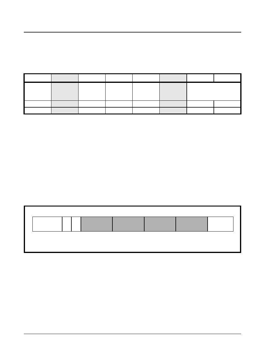
XRT7250
·Á
·Á
·Á
·Á
DS3/E3 FRAMER IC
REV. 1.1.1
234
5.0
E3/ITU-T G.751 OPERATION OF THE
XRT7250
Configuring the XRT7250 to Operate in the E3,
ITU-T G.751 Mode
The XRT7250 can be configured to operate in the E3/
ITU-T G.751 Mode by writing a "0" into bit-field 6 and
a "0" into bit-field 2, within the Framer Operating
Mode register, as illustrated below.
Prior to describing the functional blocks within the
Transmit and Receive Sections of the XRT7250, it is
important to describe the E3, ITU-T G.751 framing
format.
5.1
D
ESCRIPTION
OF
THE
E3, ITU-T G.751 F
RAMES
AND
A
SSOCIATED
O
VERHEAD
B
ITS
The role of the various overhead bytes are best de-
scribed by discussing the E3, ITU-T G.751 Frame
Format as a whole. The E3, ITU-T G.751 Frame con-
tains 1536 bits, of which 12 bits are overhead and the
remaining 1524 bits are payload bits.
Each E3, ITU-T G.751 Frame consists of the following
12 overhead bits.
∑ A 10 bit FAS (Framing Alignment Signal) pattern.
This pattern is assigned the constant pattern of
"1111010000", and is used by the Receive E3
Framer block to acquire and maintain Frame Syn-
chronization with the incoming E3 frames.
∑ The "A" (or Alarm) Bit.
∑ The "N" (or National) Bit.
∑ The BIP-4 Bits (if configured).
The frame repetition rate for this type of E3 frame is
22375 times per second, thereby resulting in the
standard E3 bit rate of 34.368 Mbps. Figure 97 pre-
sents an illustration of the E3, ITU-T G.751 Frame
Format.
5.1.1
Definition of the Overhead Bits
Each of these Overhead Bits are further defined be-
low.Frame Alignment Signaling (FAS) Pattern Bits
The first 10 bits, within each E3, ITU-T G.751 frame
are known as the FAS (or Framing Alignment Signal-
ing) bits. The Receive E3 Framer block, while trying
to acquire or maintain framing synchronization with its
incoming E3 frames, will attempt to locate the FAS
bits. The FAS pattern is assigned the value
"1111010000".
5.1.1.1
The "A" (Alarm) Bit
The "A" bit typically functions as a FERF (Far-End
Receive Failure) indicator bit. However, if the user
configures the XRT7250 Framer IC to transmit and
receive E3 frames which are carrying the BIP-4 value
(located at the end of a given E3 frame), then this bit
will also function as the FEBE indicator bit. A detailed
discussion on the practical use of the "A" is present-
ed in Section 4.2.2. Each of these roles of the "A" bit
are briefly discussed below.
The "A" Bit Functioning as the FERF bit-field
If the Receive E3 Framer block (at a Local Terminal)
is experiencing problems receiving E3 frame data
from a Remote Terminal (e.g., an LOS, OOF or AIS
FRAMER OPERATING MODE REGISTER (ADDRESS = 0X00)
B
IT
7
B
IT
6
B
IT
5
B
IT
4
B
IT
3
B
IT
2
B
IT
1
B
IT
0
Local
Loopback
DS3/E3*
Internal
LOS
Enable
RESET
Interrupt
Enable
Reset
Frame
Format
TimRefSel[1:0]
R/W
R/W
R/W
R/W
R/W
R/W
R/W
R/W
x
0
x
0
x
0
x
x
F
IGURE
97. I
LLUSTRATION
OF
THE
E3, ITU-T G.751 F
RAMING
F
ORMAT
.
Frame
Alignment
Signal
A
N
Data
Data
Data
Data
BIP-4
if Selected
1 10 11 12 384 385 768 769 1152 1153 1532 1536
Framing Alignment Signal Pattern = 1111010000
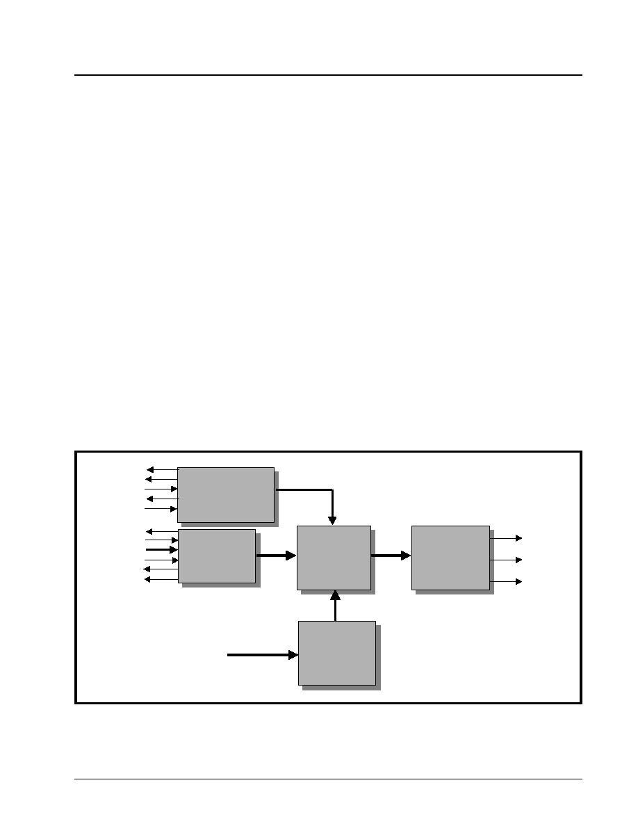
·Á
·Á
·Á
·Á
XRT7250
DS3/E3 FRAMER IC
REV. 1.1.1
235
condition), then it will inform the Remote Terminal
Equipment of this fact by commanding the Local
Transmit E3 Framer block to set the "A" bit-field, with-
in the next outbound E3 frame, to "1". The Local
Transmit E3 Framer block will continue to set the "A"
bit-field (within the subsequent outbound E3 frames)
to "1" until the Receive E3 Framer block no longer ex-
periences problems in receiving the E3 frame data. If
the Remote Terminal Equipment receives a certain
number of consecutive E3 frames, with the "A" bit-
field set to "1", then the Remote Terminal Equipment
will interpret this signaling as an indication of a Far-
End Receive Failure (e.g., a problem with the Local
Terminal Equipment).
Conversely, if the Receive E3 Framer block (at a Lo-
cal Terminal Equipment) is not experiencing any
problems receiving E3 frame data from a Remote Ter-
minal Equipment, then it will also inform the Remote
Terminal Equipment of this fact by commanding the
Local Transmit E3 Framer block to set the "A" bit-field
within an outbound E3 frame (which is destined for
the Remote Terminal) to "0". The Remote Terminal
Equipment will interpret this form of signaling as an
indication of a normal operation.
A detailed discussion into the practical use of the A
bit-field is presented in Section 4.2.2.
5.1.1.2
The "N" Bit
The "N" bit is typically used to transport PMDL (Path
Maintenance Data Link) information, from one termi-
nal to the next. However, the "N" bit-field can also be
used to transport a proprietary data link, if configured
according.
A detailed discussion into the practical use of the N-
bit field is presented in Section 4.2.2.
5.2
T
HE
T
RANSMIT
S
ECTION
OF
THE
XRT7250 (E3,
ITU-T G.751 M
ODE
O
PERATION
)
When the XRT7250 has been configured to operate
in the E3, ITU-T G.751 Mode, the Transmit Section of
the XRT7250 consists of the following functional
blocks.
∑ Transmit Payload Data Input Interface block
∑ Transmit Overhead Data Input Interface block
∑ Transmit E3 Framer block
∑ Transmit HDLC Controller block
∑ Transmit LIU Interface block
Figure 98 presents a simple illustration of the Trans-
mit Section of the XRT7250 Framer IC.
Each of these functional blocks will be discussed in
detail in this document.
5.2.1
The Transmit Payload Data Input Interface
Block
Figure 99 presents a simple illustration of the Trans-
mit Payload Data Input Interface block.
F
IGURE
98. A S
IMPLE
I
LLUSTRATION
OF
THE
XRT7250 T
RANSMIT
S
ECTION
WHEN
IT
HAS
BEEN
CONFIGURED
TO
OPERATE
IN
THE
E3 M
ODE
Transmit
Payload Data
Input
Interface Block
Transmit DS3/E3
Framer Block
Transmit LIU
Interface
Block
TxSer
TxNib[3:0]
TxInClk
TxPOS
TxNEG
TxLineClk
Transmit Overhead
Input
Interface Block
TxOHClk
TxOHIns
TxOHInd
TxOH
TxOHEnable
TxOHFrame
TxNibClk
TxFrame
Tx E3 HDLC
Controller/Buffer
Tx E3 HDLC
Controller/Buffer
From Microprocessor
Interface Block
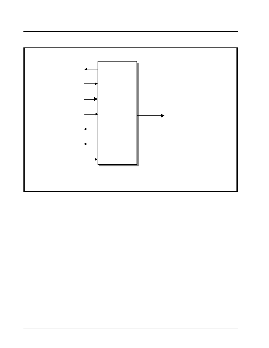
XRT7250
·Á
·Á
·Á
·Á
DS3/E3 FRAMER IC
REV. 1.1.1
236
Each of the input and output pins of the Transmit Pay-
load Data Input Interface are listed in Table 46 and
described below. The exact role that each of these
inputs and output pins assume, for a variety of operat-
ing scenarios are described throughout this section.
F
IGURE
99. A S
IMPLE
I
LLUSTRATION
OF
THE
T
RANSMIT
P
AYLOAD
D
ATA
I
NPUT
I
NTERFACE
B
LOCK
Transmit Payload
Data Input
Interface Block
Transmit Payload
Data Input
Interface Block
TxOH_Ind
TxSer
TxNib[3:0]
TxInClk
TxNibClk
TxFrame
TxFrameRef
To Transmit DS3 Framer Block

·Á
·Á
·Á
·Á
XRT7250
DS3/E3 FRAMER IC
REV. 1.1.1
237
Operation of the Transmit Payload Data Input In-
terface
The Transmit Terminal Input Interface is extremely
flexible, in that it permits the user to make the follow-
ing configuration options.
T
ABLE
46: L
ISTING
AND
D
ESCRIPTION
OF
THE
PINS
ASSOCIATED
WITH
THE
T
RANSMIT
P
AYLOAD
D
ATA
I
NPUT
I
NTERFACE
S
IGNAL
N
AME
T
YPE
D
ESCRIPTION
TxSer
Input
Transmit Serial Payload Data Input Pin:
If the user opts to operate the XRT7250 in the serial mode, then the Terminal Equipment is
expected to apply the payload data (that is to be transported via the outbound E3 data stream)
to this input pin. The XRT7250 will sample the data that is at this input pin upon the rising
edge either the RxOutClk or the TxInClk signal (whichever is appropriate).
N
OTE
: This signal is only active if the NibInt input pin is pulled "Low".
TxNib[3:0]
Input
Transmit Nibble-Parallel Payload Data Input pins:
If the user opts to operate the XRT7250 in the Nibble-Parallel mode, then the Terminal Equip-
ment is expected to apply the payload data (that is to be transported via the outbound E3 data
stream) to these input pins. The XRT7250 will sample the data that is at these input pins upon
the rising edge of the TxNibClk signal.
N
OTE
: These pins are only active if the NibInt input pin is pulled "High".
TxInClk
Input
Transmit Section Timing Reference Clock Input pin:
The Transmit Section of the XRT7250 can be configured to use this clock signal as the Timing
Reference. If the user has made this configuration selection, then the XRT7250 will use this
clock signal to sample the data on the TxSer input pin.
N
OTE
: If this configuration is selected, then a 34.368 MHz clock signal must be applied to this
input pin.
TxNibClk
Output Transmit Nibble Mode Output
If the user opts to operate the XRT7250 in the Nibble-Parallel mode, then the XRT7250 will
derive this clock signal from the selected Timing Reference for the Transmit Section of the chip
(e.g., either the TxInClk or the RxLineClk signals).
The XRT7250 will use this signal to sample the data on the TxNib[3:0] input pins.
TxOHInd
Output Transmit Overhead Bit Indicator Output:
This output pin will pulse "High" one-bit period prior to the time that the Transmit Section of the
XRT7250 will be processing an Overhead bit. The purpose of this output pin is to warn the
Terminal Equipment that, during the very next bit-period, the XRT7250 is going to be process-
ing an Overhead bit and will be ignoring any data that is applied to the TxSer input pin.
TxFrame
Output Transmit End of Frame Output Indicator:
The Transmit Section of the XRT7250 will pulse this output pin "High" (for one bit-period),
when the Transmit Payload Data Input Interface is processing the last bit of a given E3 frame.
The purpose of this output pin is to alert the Terminal Equipment that it needs to begin trans-
mission of a new E3 frame to the XRT7250 (e.g., to permit the XRT7250 to maintain Transmit
E3 framing alignment control over the Terminal Equipment).
TxFrameRef
Input
Transmit Frame Reference Input:
The XRT7250 permits the user to configure the Transmit Section to use this input pin as a
frame reference. If the user makes this configuration selection, then the Transmit Section will
initiate its transmission of a new E3 frame, upon the rising edge of this signal.
The purpose of this input pin is to permit the Terminal Equipment to maintain Transmit E3
Framing alignment control over the XRT7250.
RxOutClk
Output Loop-Timed Timing Reference Clock Output pin:
The Transmit Section of the XRT7250 can be configured to use the RxLineClk signal as the
Timing Reference (e.g., loop-timing). If the user has made this configuration selection, then
the XRT7250 will:
∑
Output a 34.368 MHz clock signal via this pin, to the Terminal Equipment.
∑
Sample the data on the TxSer input pin, upon the rising edge of this clock signal.
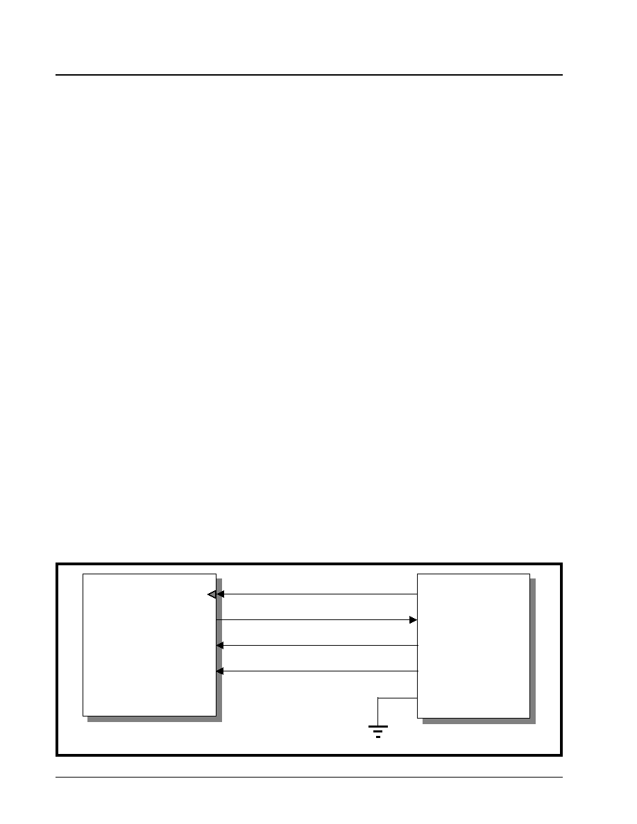
XRT7250
·Á
·Á
·Á
·Á
DS3/E3 FRAMER IC
REV. 1.1.1
238
∑ The Serial or the Nibble-Parallel Interface Mode
∑ The Loop-Timing or the TxInClk (Local Timing)
Mode
Further, if the XRT7250 has been configured to oper-
ate in the Local-Timing mode, then the user has two
additional options.
∑ The XRT7250 is the Frame Master (e.g., it dictates
when the Terminal Equipment will initiate the trans-
mission of data within a new E3 frame).
∑ The XRT7250 is the Frame Slave (e.g., the Termi-
nal Equipment will dictate when the XRT7250 ini-
tiates the transmission of a new E3 frame).
Given these three set of options, the Transmit Termi-
nal Input Interface can be configured to operate in
one of the six (6) following modes.
∑ Mode 1 - Serial/Loop-Timed Mode
∑ Mode 2 - Serial/Local-Timed/Frame Slave Mode
∑ Mode 3 - Serial/Local-Timed/Frame Master Mode
∑ Mode 4 - Nibble/Loop-Timed Mode
∑ Mode 5 - Nibble/Local-Timed/Frame Slave Mode
∑ Mode 6 - Nibble/Local-Timed/Frame Master Mode
Each of these modes are described, in detail, below.
5.2.1.1
Mode 1 - The Serial/Loop-Timing Mode
The Behavior of the XRT7250
If the XRT7250 has been configured to operate in this
mode, then the XRT7250 will behave as follows.
A. Loop-Timing (Uses the RxLineClk signal as the
Timing Reference)
Since the XRT7250 is configured to operate in the
loop-timed mode, the Transmit Section of the
XRT7250 will use the RxLineClk input clock signal
(e.g., the Recovered Clock signal, from the LIU) as its
timing source. When the XRT7250 is operating in this
mode it will do the following.
1. It will ignore any signal at the TxInClk input pin.
2. The XRT7250 will output a 34.368MHz clock sig-
nal via the RxOutClk output pin. This clock signal
functions as the Transmit Payload Data Input
Interface block clock signal.
3. The XRT7250 will use the rising edge of the
RxOutClk signal to latch in the data residing on
the TxSer input pin.
B. Serial Mode
The XRT7250 will accept the E3 payload data from
the Terminal Equipment, in a serial-manner, via the
TxSer input pin The Transmit Payload Data Input In-
terface will latch this data into its circuitry, on the ris-
ing edge of the RxOutClk output clock signal.
C. Delineation of outbound E3 frames
The XRT7250 will pulse the TxFrame output pin
"High" for one bit-period coincident with the XRT7250
processing the last bit of a given E3 frame.
D. Sampling of Payload Data, from the Terminal
Equipment
In Mode 1, the XRT7250 will sample the data at the
TxSer input, on the rising edge of RxOutClk.
Interfacing the Transmit Payload Data Input Inter-
face block of the XRT7250 to the Terminal Equip-
ment for Mode 1 Operation
Figure 100 presents an illustration of the Transmit
Payload Data Input Interface block (within the
XRT7250) being interfaced to the Terminal Equip-
ment, for Mode 1 operation.
F
IGURE
100. I
LLUSTRATION
OF
THE
T
ERMINAL
E
QUIPMENT
BEING
INTERFACED
TO
THE
T
RANSMIT
P
AYLOAD
D
ATA
I
NPUT
I
NTERFACE
BLOCK
OF
THE
XRT7250
FOR
M
ODE
1 (S
ERIAL
/L
OOP
-T
IMED
) O
PERATION
Terminal Equipment
XRT7250 E3 Framer
E3_Data_Out
E3_Clock_In
Tx_Start_of_Frame
E3_Overhead_Ind
TxSer
RxOutClk
TxFrame
TxOH_Ind
NibInt
34.368 MHz

·Á
·Á
·Á
·Á
XRT7250
DS3/E3 FRAMER IC
REV. 1.1.1
239
Mode 1 Operation of the Terminal Equipment
When the XRT7250 is operating in this mode, it will
function as the source of the 34.368MHz clock signal.
This clock signal will be used as the Terminal Equip-
ment Interface clock by both the XRT7250 IC and the
Terminal Equipment.
The Terminal Equipment will serially output the pay-
load data of the outbound E3 data stream via its
E3_Data_Out pin. The Terminal Equipment will up-
date the data on the E3_Data_Out pin upon the rising
edge of the 34.368 MHz clock signal, at its
E3_Clock_In input pin (as depicted in Figure 100 and
Figure 101).
The XRT7250 will latch the outbound E3 data stream
(from the Terminal Equipment) on the rising edge of
the RxOutClk signal.
The XRT7250 will indicate that it is processing the
last bit, within a given outbound E3 frame, by pulsing
its TxFrame output pin "High" for one bit-period.
When the Terminal Equipment detects this pulse at its
Tx_Start_of_Frame input, it is expected to begin
transmission of the very next outbound E3 frame to
the XRT7250 via the E3_Data_Out (or TxSer pin).
Finally, the XRT7250 will indicate that it is about to
process an overhead bit by pulsing the TxOH_Ind
output pin "High" one bit period prior to its processing
of an OH (Overhead) bit. In Figure 100, the
TxOH_Ind output pin is connected to the
E3_Overhead_Ind input pin of the Terminal Equip-
ment. Whenever the E3_Overhead_Ind pin is pulsed
"High" the Terminal Equipment is expected to not
transmit a E3 payload bit upon the very next clock
edge. Instead, the Terminal Equipment is expected to
delay its transmission of the very next payload bit, by
one clock cycle.
The behavior of the signals, between the XRT7250
and the Terminal Equipment, for E3 Mode 1 operation
is illustrated in Figure 101.
Inserting the A and N bits into the outbound E3
frames via the Transmit Payload Data Input Inter-
face block
The XRT7250 DS3/E3 Framer permits the Terminal
Equipment to insert its own values for the "A" and/or
"N" bits, into the outbound E3 frame, via the Transmit
Payload Data Input Interface block. If the user de-
sires to do this, the XRT7250 Framer IC must be con-
figured to accept the Terminal Equipment's value for
the "A" and "N" bits, by writing to appropriate data into
the TxASourceSel[1:0] and TxNSourceSel[1:0] bit-
fields, within the TxE3 Configuration Register (Ad-
dress =0x30), as illustrated below.
Configuring the Transmit Payload Data Input In-
terface block to accept the "A Bits" from the Ter-
minal Equipment
If the user wishes to configure the Transmit Payload
Data Input Interface block to accept the "A" bits from
the Terminal Equipment, then the user must write the
value "10" into the TxASourceSel[1:0] bit-fields.
Once the user does this, then any value, which re-
sides on the TxSer input pin, when the "A" bit is being
processed by the Transmit Section will be inserted in-
to the "A" bit-field within the very next outbound E3
frame.
For completeness, the relationship between the con-
tents of the TxASourceSel[1:0] bits and the resulting
source of the "A" bit is listed below.
Bit 6, 5, TxASourceSel[1:0]
These two Read/Write bit-fields combine to specify
the source of the A-bit, within each outbound E3
frame. The relationship between these two bit-fields
and the resulting source of the A Bit is tabulated be-
low.
TXE3 CONFIGURATION REGISTER (ADDRESS = 0X30)
B
IT
7
B
IT
6
B
IT
5
B
IT
4
B
IT
3
B
IT
2
B
IT
1
B
IT
0
Tx
BIP-4
Enable
TxASourceSel[1:0]
TxNSourceSel[1:0]
Tx AIS
Enable
Tx LOS
Enable
Tx FAS
Source
Select
R/W
R/W
R/W
R/W
R/W
R/W
R/W
R/W
0
X
X
X
X
0
0
0
T
X
AS
OURCE
S
EL
[1:0]
S
OURCE
OF
A B
IT
00
TxE3 Service Bits Register (Address = 0x35)

XRT7250
·Á
·Á
·Á
·Á
DS3/E3 FRAMER IC
REV. 1.1.1
240
Configuring the Transmit Payload Data Input Interface
block to accept the "N" Bits from the Terminal Equip-
ment, then the user must write the value "11" into the
TxNSourceSel[1:0] bit-fields. Once the user does
this, then any value, which resides on the TxSer input
pin, when the "N" bit is being processed by the Trans-
mit Section will be inserted into the "N" bit-field within
the very next outbound E3 frame.
For completeness, the relationship between the con-
tents of the TxNSourceSel[1:0] bits and the resulting
source of the "N" bit is listed below.
Bits 4, 3, TxNSourceSel[1:0]
These two Read/Write bit-fields combine to specify
the source of the N-bit, within each outbound E3
frame. The relationship between these two bit-fields
and the resulting source of the N Bit is tabulated be-
low.
01
Transmit Overhead Data Input Interface
10
Transmit Payload Data Input Interface
11
Functions as a FEBE (Far-End-Block Error) bit-field.
This bit-field is set to "0", if the Near-End Receive Section (within this chip) detects no BIP-4
Errors within the incoming E3 frames.
This bit-field is set to "1", if the Near-End Receive Section (within this chip) detects a BIP-4
Error within the incoming E3 frame.
T
X
AS
OURCE
S
EL
[1:0]
S
OURCE
OF
A B
IT
T
X
NS
OURCE
S
EL
[1:0]
S
OURCE
OF
N B
IT
00
TxE3 Service Bits Register (Address = 0x35)
01
Transmit Overhead Data Input Interface
10
Transmit LAPD Controller
11
Transmit Payload Data Input Interface
.
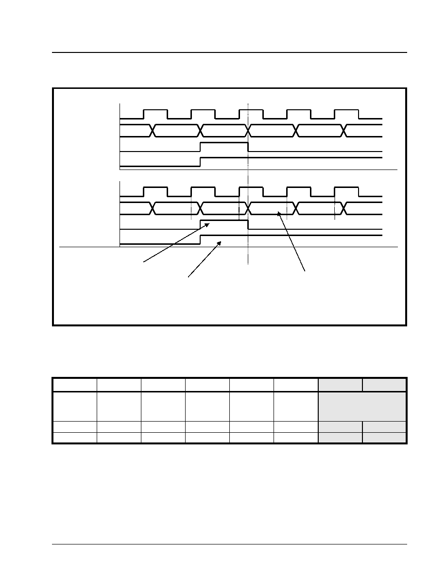
·Á
·Á
·Á
·Á
XRT7250
DS3/E3 FRAMER IC
REV. 1.1.1
241
How to configure the XRT7250 into the Serial/
Loop-Timed/Non-Overhead Interface Mode
1. Set the NibIntf input pin "Low".
2. Set the TimRefSel[1:0] bit fields (within the
Framer Operating Mode Register) to "00", as
illustrated below.
3. Interface the XRT7250, to the Terminal Equip-
ment, as illustrated in Figure 100.
5.2.1.2
Mode 2 - The Serial/Local-Timed/
Frame-Slave Mode Behavior of the XRT7250
If the XRT7250 has been configured to operate in this
mode, then the XRT7250 will function as follows.
A. Local-Timed - Uses the TxInClk signal as the
Timing Reference
In this mode, the Transmit Section of the XRT7250
will use the TxInClk signal as its timing reference.
B. Serial Mode
The XRT7250 will receive the E3 payload data, in a
serial manner, via the TxSer input pin. The Transmit
Payload Data Input Interface (within the XRT7250)
will latch this data into its circuitry, on the rising edge
of the TxInClk input clock signal.
F
IGURE
101. B
EHAVIOR
OF
THE
T
ERMINAL
I
NTERFACE
SIGNALS
BETWEEN
THE
XRT7250 T
RANSMIT
P
AYLOAD
D
ATA
I
NPUT
I
NTERFACE
BLOCK
AND
THE
T
ERMINAL
E
QUIPMENT
(
FOR
M
ODE
1 O
PERATION
)
Terminal Equipment Signals
E3_Clock_In
E3_Data_Out
Tx_Start_of_Frame
E3_Overhead_Ind
XRT7250 Transmit Payload Data I/F Signals
RxOutClk
TxSer
TxFrame
TxOH_Ind
Payload[1522]
Payload[1523]
FAS, Bit 9
FAS, Bit 8
Payload[1522]
Payload[1523]
FAS, Bit 9
FAS, Bit 8
Note: The FAS pattern will not be processed by the
Transmit Payload Data Input Interface.
E3 Frame Number N
E3 Frame Number N + 1
Note: TxFrame pulses high to denote
E3 Frame Boundary.
Note: TxOH_Ind pulses high for
12 bit periods in order to
denote Overhead Data
(e.g., the FAS pattern and the
A & N bits).
FRAMER OPERATING MODE REGISTER (ADDRESS = 0X00)
B
IT
7
B
IT
6
B
IT
5
B
IT
4
B
IT
3
B
IT
2
B
IT
1
B
IT
0
Local
Loopback
DS3/E3*
Internal
LOS
Enable
RESET
Interrupt
Enable
Reset
Frame
Format
TimRefSel[1:0]
R/W
R/W
R/W
R/W
R/W
R/W
R/W
R/W
0
0
1
0
1
0
0
0
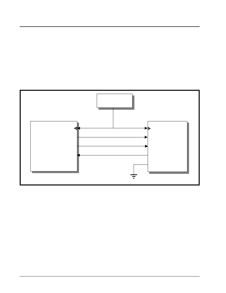
XRT7250
·Á
·Á
·Á
·Á
DS3/E3 FRAMER IC
REV. 1.1.1
242
C. Delineation of outbound E3 frames (Frame
Slave Mode)
The Transmit Section of the XRT7250 will use the Tx-
InClk input as its timing reference, and will use the
TxFrameRef input signal as its framing reference. In
other words, the Transmit Section of the XRT7250 will
initiate frame generation upon the rising edge of the
TxFrameRef input signal).
D. Sampling of payload data, from the Terminal
Equipment
In Mode 2, the XRT7250 will sample the data, at the
TxSer input pin, on the rising edge of TxInClk.
Interfacing the Transmit Payload Data Input Inter-
face block of the XRT7250 to the Terminal Equip-
ment for Mode 2 Operation
Figure 102 presents an illustration of the Transmit
Payload Data Input Interface block (within the
XRT7250) being interfaced to the Terminal Equip-
ment, for Mode 2 operation.
Mode 2 Operation of the Terminal Equipment
As shown in Figure 102, both the Terminal Equipment
and the XRT7250 will be driven by an external
34.368MHz clock signal. The Terminal Equipment
will receive the 34.368MHz clock signal via its
E3_Clock_In input pin, and the XRT7250 Framer IC
will receive the 34.368MHz clock signal via the TxIn-
Clk input pin.
The Terminal Equipment will serially output the pay-
load data of the outbound E3 data stream, via the
E3_Data_Out output pin, upon the rising edge of the
signal at the E3_Clock_In input pin.
N
OTE
: The E3_Data_Out output pin of the Terminal Equip-
ment is electrically connected to the TxSer input pin
The XRT7250 Framer IC will latch the data, residing
on the TxSer input line, on the rising edge of the TxIn-
Clk signal.
In this case, the Terminal Equipment has the respon-
sibility of providing the framing reference signal by
pulsing its Tx_Start_of_Frame output signal (and in
turn, the TxFrameRef input pin of the XRT7250),
"High" for one-bit period, coincident with the first bit of
a new E3 frame. Once the XRT7250 detects the ris-
ing edge of the input at its TxFrameRef input pin, it
will begin generation of a new E3 frame.
N
OTES
:
1. In this case, the Terminal Equipment is controlling
the start of Frame Generation, and is therefore
referred to as the Frame Master. Conversely, since
the XRT7250 does not control the generation of a
new E3 frame, but is rather driven by the Terminal
Equipment, the XRT7250 is referred to as the
Frame Slave.
2. If the user opts to configure the XRT7250 to oper-
ate in Mode 2, it is imperative that the
F
IGURE
102. I
LLUSTRATION
OF
THE
T
ERMINAL
E
QUIPMENT
BEING
INTERFACED
TO
THE
T
RANSMIT
P
AYLOAD
D
ATA
I
NPUT
I
NTERFACE
BLOCK
OF
THE
XRT7250
FOR
M
ODE
2 (S
ERIAL
/L
OCAL
-T
IMED
/F
RAME
-S
LAVE
) O
PERATION
Terminal Equipment
XRT7250 E3 Framer
E3_Data_Out
E3_Clock_In
Tx_Start_of_Frame
E3_Overhead_Ind
TxSer
TxInClk
TxFrameRef
TxOH_Ind
NibInt
34.368 MHz Clock
Source
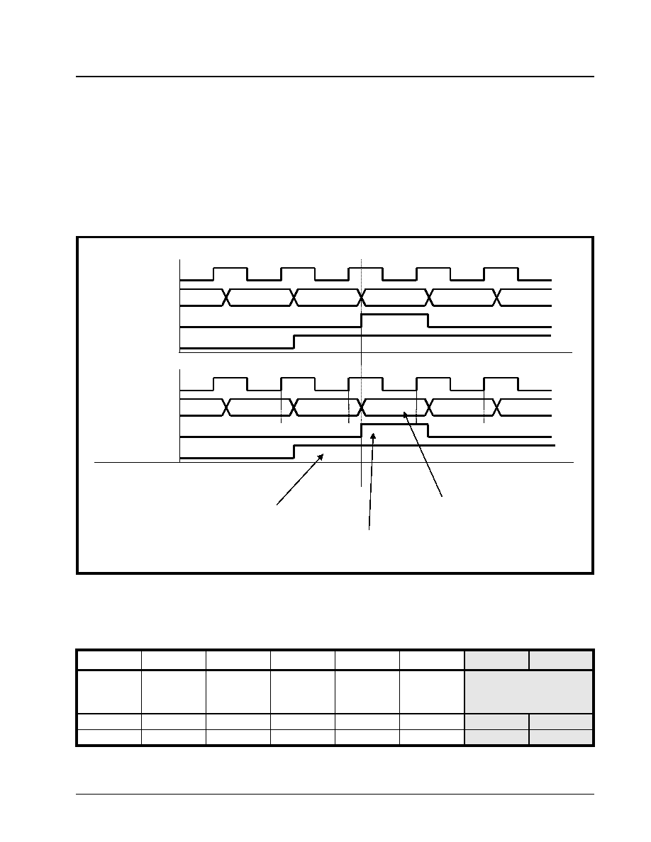
·Á
·Á
·Á
·Á
XRT7250
DS3/E3 FRAMER IC
REV. 1.1.1
243
Tx_Start_of_Frame (or TxFrameRef) signal is syn-
chronized to the TxInClk input clock signal.
Finally, the XRT7250 will pulse its TxOH_Ind output
pin, one bit-period prior to it processing a given over-
head bit, within the outbound E3 frame. Since the
TxOH_Ind output pin of the XRT7250 is electrically
connected to the E3_Overhead_Ind whenever the
XRT7250 pulses the TxOH_Ind output pin "High", it
will also be driving the E3_Overhead_Ind input pin (of
the Terminal Equipment) "High". Whenever the Ter-
minal Equipment detects this pin toggling "High", it
should delay transmission of the very next E3 frame
payload bit by one clock cycle.
The behavior of the signals between the XRT7250
and the Terminal Equipment for E3 Mode 2 Operation
is illustrated in Figure 103.
How to configure the XRT7250 to operate in this
mode.
1. Set the NibIntf input pin "Low".
2. Set the TimRefSel[1:0] bit-fields (within the
Framer Operating Mode Register) to "01" as
depicted below.
3. Interface the XRT7250, to the Terminal Equip-
ment, as illustrated in Figure 102.
5.2.1.3
Mode 3 - The Serial/Local-Timed/
Frame-Master Mode Behavior of the XRT7250
F
IGURE
103. B
EHAVIOR
OF
THE
T
ERMINAL
I
NTERFACE
SIGNALS
BETWEEN
THE
XRT7250
AND
THE
T
ERMINAL
E
QUIPMENT
(M
ODE
2 O
PERATION
)
Terminal Equipment Signals
E3_Clock_In
E3_Data_Out
Tx_Start_of_Frame
E3_Overhead_Ind
XRT7250 Transmit Payload Data I/F Signals
TxInClk
TxSer
TxFrameRef
TxOH_Ind
Payload[1522]
Payload[1523]
FAS, Bit 9
FAS, Bit 8
Payload[1522]
Payload[1523]
FAS, Bit 9
FAS, Bit 8
Note: FAS Pattern bits will not be processed by the
Transmit Payload Data Input Interface.
E3 Frame Number N
E3 Frame Number N + 1
Note: TxFrame pulses high to denote
E3 Frame Boundary.
Note: TxOH_Ind pulses high for
12 bit periods in order to
denote Overhead Data
(e.g., the FAS pattern
and the A & N bits).
FRAMER OPERATING MODE REGISTER (ADDRESS = 0X00)
B
IT
7
B
IT
6
B
IT
5
B
IT
4
B
IT
3
B
IT
2
B
IT
1
B
IT
0
Local
Loopback
DS3/E3*
Internal
LOS
Enable
RESET
Interrupt
Enable
Reset
Frame
Format
TimRefSel[1:0]
R/W
R/W
R/W
R/W
R/W
R/W
R/W
R/W
0
0
1
0
1
0
0
1
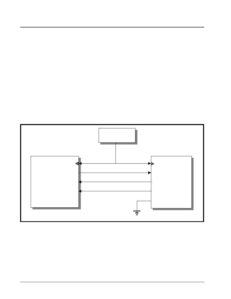
XRT7250
·Á
·Á
·Á
·Á
DS3/E3 FRAMER IC
REV. 1.1.1
244
If the XRT7250 has been configured to operate in this
mode, then the XRT7250 will function as follows.
A. Local-Timed - Uses the TxInClk signal as the
Timing Reference
In this mode, the Transmit Section of the XRT7250
will use the TxInClk signal as its timing reference.
B. Serial Mode
The XRT7250 will receive the E3 payload data, in a
serial manner, via the TxSer input pin. The Transmit
Payload Data Input Interface (within the XRT7250)
will latch this data into its circuitry, on the rising edge
of the TxInClk input clock signal.
C. Delineation of outbound DS3 frames (Frame
Master Mode)
The Transmit Section of the XRT7250 will use the Tx-
InClk signal as its timing reference, and will initiate E3
frame generation, asynchronously with respect to any
externally applied signal. The XRT7250 will pulse its
TxFrame output pin "High" whenever its it processing
the very last bit-field within a given E3 frame.
D. Sampling of payload data, from the Terminal
Equipment
In Mode 3, the XRT7250 will sample the data, at the
TxSer input pin, on the rising edge of TxInClk.
Interfacing the Transmit Payload Data Input Inter-
face block of the XRT7250 to the Terminal Equip-
ment for Mode 3 Operation
Figure 104 presents an illustration of the Transmit
Payload Data Input Interface block (within the
XRT7250) being interfaced to the Terminal Equip-
ment, for Mode 3 operation.
Mode 3 Operation of the Terminal Equipment
In Figure 104, both the Terminal Equipment and the
XRT7250 are driven by an external 34.368 MHz clock
signal. This clock signal is connected to the
E3_Clock_In input of the Terminal Equipment and the
TxInClk input pin of the XRT7250.
The Terminal Equipment will serially output the pay-
load data on its E3_Data_Out output pin, upon the
rising edge of the signal at the E3_Clock_In input pin.
Similarly, the XRT7250 will latch the data, residing on
the TxSer input pin, on the rising edge of TxInClk.
The XRT7250 will pulse the TxFrame output pin
"High" for one bit-period, coincident while it is pro-
cessing the last bit-field within a given outbound E3
frame. The Terminal Equipment is expected to moni-
tor the TxFrame signal (from the XRT7250) and to
place the first bit, within the very next outbound E3
frame on the TxSer input pin.
N
OTE
: In this case, the XRT7250 dictates exactly when the
very next E3 frame will be generated. The Terminal Equip-
ment is expected to respond appropriately by providing the
XRT7250 with the first bit of the new E3 frame, upon
demand. Hence, in this mode, the XRT7250 is referred to
F
IGURE
104. I
LLUSTRATION
OF
THE
T
ERMINAL
E
QUIPMENT
BEING
INTERFACED
TO
THE
T
RANSMIT
P
AYLOAD
D
ATA
I
NPUT
I
NTERFACE
BLOCK
OF
THE
XRT7250
FOR
M
ODE
3 (S
ERIAL
/L
OCAL
-T
IME
/F
RAME
-M
ASTER
) O
PERATION
Terminal Equipment
XRT7250 E3 Framer
E3_Data_Out
E3_Clock_In
Tx_Start_of_Frame
E3_Overhead_Ind
TxSer
TxInClk
TxFrame
TxOH_Ind
NibInt
34.368 MHz Clock
Source
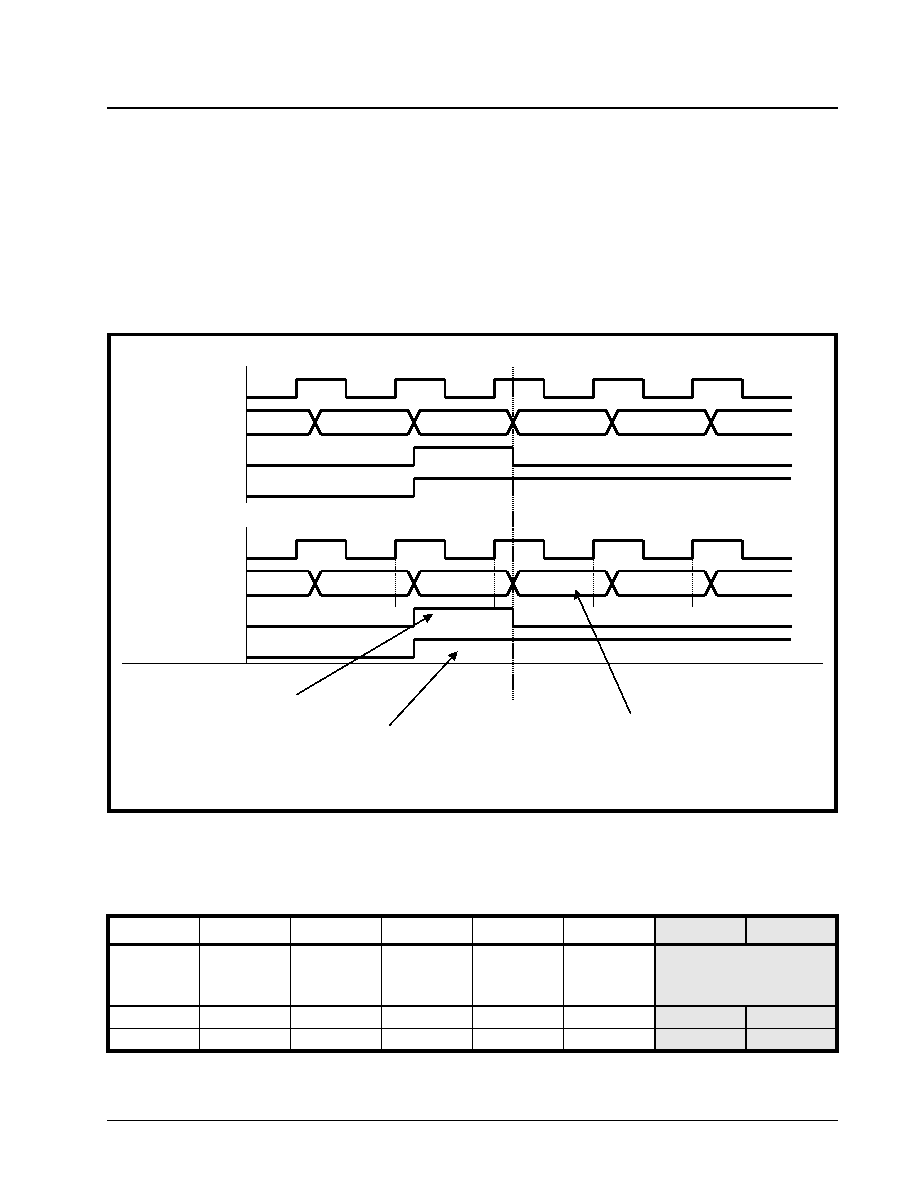
·Á
·Á
·Á
·Á
XRT7250
DS3/E3 FRAMER IC
REV. 1.1.1
245
as the Frame Master and the Terminal Equipment is
referred to as the Frame Slave.
Finally, the XRT7250 will pulse its TxOH_Ind output
pin, one bit-period prior to it processing a given over-
head bit, within the outbound E3 frame. Since the
TxOH_Ind output pin (of the XRT7250) is electrically
connected to the E3_Overhead_Ind whenever the
XRT7250 pulses the TxOH_Ind output pin "High", it
will also be driving the E3_Overhead_Ind input pin (of
the Terminal Equipment) "High". Whenever the Ter-
minal Equipment detects this pin toggling "High", it
should delay transmission of the very next DS3 frame
payload bit by one clock cycle.
The behavior of the signal between the XRT7250 and
the Terminal Equipment for E3 Mode 3 Operation is il-
lustrated in Figure 105.
How to configure the XRT7250 to operate in this
mode.
1. Set the NibIntf input pin "Low".
2. Set the TimRefSel[1:0] bit-fields (within the
Framer Operating Mode Register) to "01" as
depicted below.
3. Interface the XRT7250, to the Terminal Equip-
ment, as illustrated in Figure 104.
5.2.1.4
Mode 4 - The Nibble-Parallel/Loop-
Timed Mode Behavior of the XRT7250
F
IGURE
105. B
EHAVIOR
OF
THE
T
ERMINAL
I
NTERFACE
SIGNALS
BETWEEN
THE
XRT7250
AND
THE
T
ERMINAL
E
QUIP
-
MENT
(E3 M
ODE
3 O
PERATION
)
Terminal Equipment Signals
E3_Clock_In
E3_Data_Out
Tx_Start_of_Frame
E3_Overhead_Ind
XRT7250 Transmit Payload Data I/F Signals
TxInClk
TxSer
TxFrame
TxOH_Ind
Payload[1522]
Payload[1523]
FAS , Bit 9
FAS, Bit 8
Payload[1522]
Payload[1523]
FAS, Bit 9
FAS, Bit 8
Note: FAS pattern will not be processed by the
Transmit Payload Data Input Interface.
E3 Frame Number N
E3 Frame Number N + 1
Note: TxFrame pulses high to denote
E3 Frame Boundary.
Note: TxOH_Ind pulses high for 12
bit-periods in order to denote
Overhead Data (e.g., the FAS pattern,
the A and N bits).
FRAMER OPERATING MODE REGISTER (ADDRESS = 0X00)
B
IT
7
B
IT
6
B
IT
5
B
IT
4
B
IT
3
B
IT
2
B
IT
1
B
IT
0
Local
Loopback
DS3/E3*
Internal
LOS
Enable
RESET
Interrupt
Enable
Reset
Frame
Format
TimRefSel[1:0]
R/W
R/W
R/W
R/W
R/W
R/W
R/W
R/W
0
0
1
0
1
0
0
0
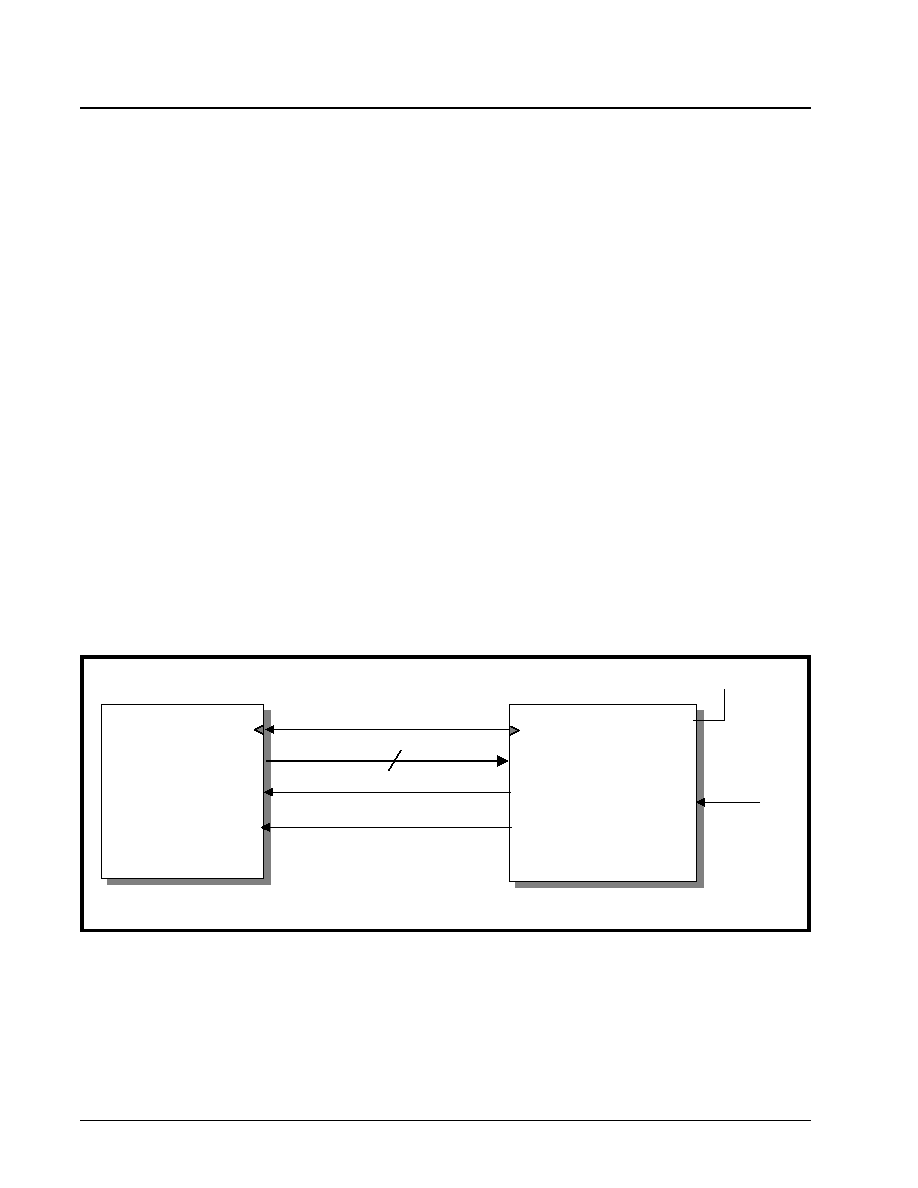
XRT7250
·Á
·Á
·Á
·Á
DS3/E3 FRAMER IC
REV. 1.1.1
246
If the XRT7250 has been configured to operate in this
mode, then the XRT7250 will behave as follows.
A. Looped Timing (Uses the RxLineClk as the
Timing Reference)
In this mode, the Transmit Section of the XRT7250
will use the RxLineClk signal as its timing reference.
When the XRT7250 is operating in the Nibble-Mode,
it will internally divide the RxLineClk signal, by a fac-
tor of four (4) and will output this signal via the TxNib-
Clk output pin.
B. Nibble-Parallel Mode
The XRT7250 will accept the E3 payload data, from
the Terminal Equipment in a nibble-parallel manner,
via the TxNib[3:0] input pins. The Transmit Terminal
Equipment Input Interface block will latch this data in-
to its circuitry, on the rising edge of the TxNibClk out-
put signal.
C. Delineation of the outbound E3 frames
The XRT7250 will pulse the TxNibFrame output pin
"High" for one bit-period coincident with the XRT7250
processing the last nibble of a given E3 frame.
D. Sampling of payload data, from the Terminal
Equipment
In Mode 4, the XRT7250 will sample the data, at the
TxNib[3:0] input pins, on the third rising edge of the
RxOutClk clock signal, following a pulse in the TxNib-
Clk signal (see Figure 107).
N
OTE
: The TxNibClk signal, from the XRT7250 operates
nominally at 8.592 MHz (e.g., 34.368 MHz divided by 4).
The E3 Frame consists of 1536 bits or 384 nibbles.
Therefore, the XRT7250 will supply 384 TxNibClk
pulses between the rising edges of two consecutive
TxNibFrame pulses. The E3 Frame repetition rate is
22.375kHz. Hence, 384 TxNibClk pulses for each E3
frame period amounts to TxNibClk running at approx-
imately 8.592 MHz. The method by which the 384
TxNibClk pulses are distributed throughout the E3
frame period is presented below.
Nominally, the Transmit Section within the XRT7250
will generate a TxNibClk pulse for every 4 RxOutClk
(or TxInClk) periods.
Interfacing the Transmit Payload Data Input Inter-
face block of the XRT7250 to the Terminal Equip-
ment for Mode 4 Operation
Figure 106 presents an illustration of the Transmit
Payload Data Input Interface block (within the
XRT7250) being interfaced to the Terminal Equip-
ment, for Mode 4 Operation.
Mode 4 Operation of the Terminal Equipment
When the XRT7250 is operating in this mode, it will
function as the source of the 8.592MHz (e.g., the
34.368MHz clock signal divided by 4) clock signal,
that will be used as the Terminal Equipment Interface
clock by both the XRT7250 and the Terminal Equip-
ment.
The Terminal Equipment will output the payload data
of the outbound E3 data stream via its
E3_Data_Out[3:0] pins on the rising edge of the
8.592MHz clock signal at the E3_Nib_Clock_In input
pin.
The XRT7250 will latch the outbound E3 data stream
(from the Terminal Equipment) on the rising edge of
the TxNibClk output clock signal. The XRT7250 will
F
IGURE
106. I
LLUSTRATION
OF
THE
T
ERMINAL
E
QUIPMENT
BEING
INTERFACED
TO
THE
T
RANSMIT
P
AYLOAD
D
ATA
I
NPUT
I
NTERFACE
BLOCK
OF
THE
XRT7250
FOR
M
ODE
4 (N
IBBLE
-P
ARALLEL
/L
OOP
-T
IMED
) O
PERATION
Terminal Equipment
XRT7250 E3 Framer
E3_Data_Out[3:0]
E3_Nib_Clock_In
Tx_Start_of_Frame
TxNib[3:0]
TxNibClk
TxNibFrame
NibInt
VCC
4
RxLineClk
34.368MHz
8.592 MHz
TxOH_Ind
E3_Overhead_Ind
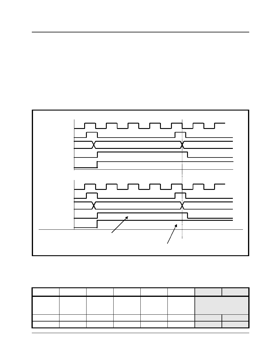
·Á
·Á
·Á
·Á
XRT7250
DS3/E3 FRAMER IC
REV. 1.1.1
247
indicate that it is processing the last nibble, within a
given E3 frame, by pulsing its TxNibFrame output pin
"High" for one TxNibClk clock period. When the Ter-
minal Equipment detects a pulse at its
Tx_Start_of_Frame input pin, it is expected to trans-
mit the first nibble, of the very next outbound E3
frame to the XRT7250 via the E3_Data_Out[3:0] (or
TxNib[3:0] pins).
Finally, for the Nibble-Parallel Mode operation, the
XRT7250 will pulse the TxOHInd output pin "High" for
3 nibble-periods (e.g., the 3 nibbles consisting of the
10 bit FAS pattern, the "A" and the "N" bits). The Tx-
OHInd output pin will remain "Low" for the remainder
of the frame period. The TxOHInd output pin will tog-
gle "High" one-nibble period before the Transmit Sec-
tion (of the Framer IC) processes the first four bits of
the FAS pattern.
The behavior of the signals between the XRT7250
and the Terminal Equipment for E3 Mode 4 Operation
is illustrated in Figure 107.
How to configure the XRT7250 into Mode 4
1. Set the NibIntf input pin "High".
2. Set the TimRefSel[1:0] bit-fields (within the
Framer Operating Mode Register) to "00" as illus-
trated below.
F
IGURE
107. B
EHAVIOR
OF
THE
T
ERMINAL
I
NTERFACE
SIGNALS
BETWEEN
THE
XRT7250
AND
THE
T
ERMINAL
E
QUIP
-
MENT
(M
ODE
4 O
PERATION
)
Terminal Equipment Signals
RxOutClk
Tx_Start_of_Frame
E3_Nib_Clock_In
E3_Data_Out[3:0]
Payload Nibble [380]
Overhead Nibble [0]
XRT7250 Transmit Payload Data I/F Signals
E3 Frame Number N
E3 Frame Number N + 1
Note: TxNibFrame pulses high to denote
E3 Frame Boundary.
RxOutClk
TxNibFrame
TxNibClk
TxNib[3:0]
Nibble [380]
Overhead Nibble [0]
E3_Overhead_Ind
TxOH_Ind
TxOH_Ind pulses high for 3 Nibble periods
FRAMER OPERATING MODE REGISTER (ADDRESS = 0X00)
B
IT
7
B
IT
6
B
IT
5
B
IT
4
B
IT
3
B
IT
2
B
IT
1
B
IT
0
Local
Loopback
DS3/E3*
Internal
LOS
Enable
RESET
Interrupt
Enable
Reset
Frame
Format
TimRefSel[1:0]
R/W
R/W
R/W
R/W
R/W
R/W
R/W
R/W
0
0
1
0
1
0
0
0

XRT7250
·Á
·Á
·Á
·Á
DS3/E3 FRAMER IC
REV. 1.1.1
248
3. Interface the XRT7250, to the Terminal Equip-
ment, as illustrated in Figure 106.
N
OTE
: The XRT7250 Framer IC cannot support the Framer
Local Loop-back Mode of operation, while operating in
Mode 4. The user must configure the XRT7250 Framer IC
into any of the following modes prior to configuring the
Framer Local Loop-back Mode operation.
∑ Mode 2 - Serial/Local-Timed/Frame-Slave Mode
∑ Mode 3 - Serial/Local-Timed/Frame-Master Mode
∑ Mode 5 - Nibble-Parallel/Local-Timed/Frame-Slave
Mode
∑ Mode 6 - Nibble-Parallel/Local-Timed/Frame-Mas-
ter Mode.
For more detailed information on the Framer Local
Loop-back Mode, please see Section 6.0.
5.2.1.5
Mode 5 - The Nibble-Parallel/Local-
Timed/Frame-Slave Interface Mode Behavior of
the XRT7250
If the XRT7250 has been configured to operate in this
mode, then the XRT7250 will function as follows:
A. Local-Timed - Uses the TxInClk signal as the
Timing Reference
In this mode, the Transmit Section of the XRT7250
will use the TxInClk signal at its timing reference.
Further, the chip will internally divide the TxInClk
clock signal by a factor of 4 and will output this divid-
ed clock signal via the TxNibClk output pin. The
Transmit Terminal Equipment Input Interface block
(within the XRT7250) will use the rising edge of the
TxNibClk signal, to latch the data, residing on the Tx-
Nib[3:0] into its circuitry.
B. Nibble-Parallel Mode
The XRT7250 will accept the E3 payload data, from
the Terminal Equipment, in a parallel manner, via the
TxNib[3:0] input pins. The Transmit Terminal Equip-
ment Input Interface will latch this data into its circuit-
ry, on the rising edge of the TxNibClk output signal.
C. Delineation of outbound E3 Frames
The Transmit Section will use the TxInClk input signal
as its timing reference and will use the TxFrameRef
input signal as its Framing Reference (e.g., the Trans-
mit Section of the XRT7250 initiates frame generation
upon the rising edge of the TxFrameRef signal).
D. Sampling of payload data, from the Terminal
Equipment
In Mode 5, the XRT7250 will sample the data, at the
TxNib[3:0] input pins, on the third rising edge of the
TxInClk clock signal, following a pulse in the TxNibClk
signal (see Figure 108).
N
OTE
: The TxNibClk signal, from the XRT7250 operates
nominally at 8.592 MHz (e.g., 34.368 MHz divided by 4).
Interfacing the Transmit Payload Data Input Inter-
face block of the XRT7250 to the Terminal Equip-
ment for Mode 5 Operation
Figure 108 presents an illustration of the Transmit
Payload Data Input Interface block (within the
XRT7250) being interfaced to the Terminal Equip-
ment, for Mode 5 Operation.

·Á
·Á
·Á
·Á
XRT7250
DS3/E3 FRAMER IC
REV. 1.1.1
249
Mode 5 Operation of the Terminal Equipment
In Figure 108 both the Terminal Equipment and the
XRT7250 will be driven by an external 8.592MHz
clock signal. The Terminal Equipment will receive the
8.592MHz clock signal via the E3_Nib_Clock_In input
pin. The XRT7250 will output the 8.592MHz clock
signal via the TxNibClk output pin.
The Terminal Equipment will serially output the data
on the E3_Data_Out[3:0] pins, upon the rising edge
of the signal at the E3_Clock_In input pin.
N
OTE
: The E3_Data_Out[3:0] output pins of the Terminal
Equipment is electrically connected to the TxNib[3:0] input
pins.
The XRT7250 will latch the data, residing on the Tx-
Nib[3:0] input pins, on the rising edge of the TxNibClk
signal.
In this case, the Terminal Equipment has the respon-
sibility of providing the framing reference signal by
pulsing the Tx_Start_of_Frame output pin (and in
turn, the TxFrameRef input pin of the XRT7250)
"High" for one bit-period, coincident with the first bit of
a new E3 frame. Once the XRT7250 detects the ris-
ing edge of the input at its TxFrameRef input pin, it
will begin generation of a new E3 frame.
Finally, the XRT7250 will always internally generate
the Overhead bits, when it is operating in both the E3
and Nibble-parallel modes. The XRT7250 will pull the
TxOHInd input pin "Low".
The behavior of the signals between the XRT7250
and the Terminal Equipment for E3 Mode 5 Operation
is illustrated in Figure 109.
F
IGURE
108. I
LLUSTRATION
OF
THE
T
ERMINAL
E
QUIPMENT
BEING
INTERFACED
TO
THE
T
RANSMIT
P
AYLOAD
D
ATA
I
NPUT
I
NTERFACE
BLOCK
OF
THE
XRT7250
FOR
M
ODE
5 (N
IBBLE
-P
ARALLEL
/L
OCAL
-T
IMED
/F
RAME
-S
LAVE
) O
PERA
-
TION
Terminal Equipment
XRT7250 E3 Framer
E3_Data_Out[3:0]
E3_Nib_Clock_In
Tx_Start_of_Frame
TxNib[3:0]
TxNibClk
TxFrameRef
NibInt
VCC
4
34.368MHz Clock Source
TxInClk
8.592MHz
E3_Overhead_Ind
TxOH_Ind

XRT7250
·Á
·Á
·Á
·Á
DS3/E3 FRAMER IC
REV. 1.1.1
250
How to configure the XRT7250 into Mode 5
1. Set the NibIntf input pin "High".
2. Set the TimRefSel[1:0] bit-fields (within the
Framer Operating Mode Register) to "01" as illus-
trated below.
3. Interface the XRT7250, to the Terminal Equip-
ment, as illustrated in Figure 108.
5.2.1.6
4.2.1.6 Mode 6 - The Nibble-Parallel/
Local-Timed/Frame-Master Interface Mode
Behavior of the XRT7250
If the XRT7250 has been configured to operate in this
mode, then the XRT7250 will function as follows:
A. Local-Timed - Uses the TxInClk signal as the
Timing Reference
In this mode, the Transmit Section of the XRT7250
will use the TxInClk signal at its timing reference.
Further, the chip will internally divide the TxInClk
clock signal by a factor of 4 and will output this divid-
ed clock signal via the TxNibClk output pin. The
Transmit Terminal Equipment Input Interface block
(within the XRT7250) will use the rising edge of the
TxNibClk signal, to latch the data, residing on the Tx-
Nib[3:0] into its circuitry.
F
IGURE
109. B
EHAVIOR
OF
THE
T
ERMINAL
I
NTERFACE
SIGNALS
BETWEEN
THE
XRT7250
AND
THE
T
ERMINAL
E
QUIPMENT
(E3, M
ODE
5 O
PERATION
)
Terminal Equipment Signals
TxInClk
Tx_Start_of_Frame
E3_Nib_Clock_In
E3_Data_Out[3:0]
Payload Nibble [380]
Overhead Nibble [0]
XRT7250 Transmit Payload Data I/F Signals
E3 Frame Number N
E3 Frame Number N + 1
Note: Terminal Equipment pulses
"TxFrameRef" in order to denote
the E3 Frame Boundary.
TxInClk
TxFrameRef
TxNibClk
TxNib[3:0]
Nibble [380]
Overhead Nibble [0]
E3_Overhead_Ind
TxOH_Ind
TxOH_Ind pulses high for 3 Nibble periods
FRAMER OPERATING MODE REGISTER (ADDRESS = 0X00)
B
IT
7
B
IT
6
B
IT
5
B
IT
4
B
IT
3
B
IT
2
B
IT
1
B
IT
0
Local
Loopback
DS3/E3*
Internal
LOS
Enable
RESET
Interrupt
Enable
Reset
Frame
Format
TimRefSel[1:0]
R/W
R/W
R/W
R/W
R/W
R/W
R/W
R/W
0
0
1
0
1
0
0
1
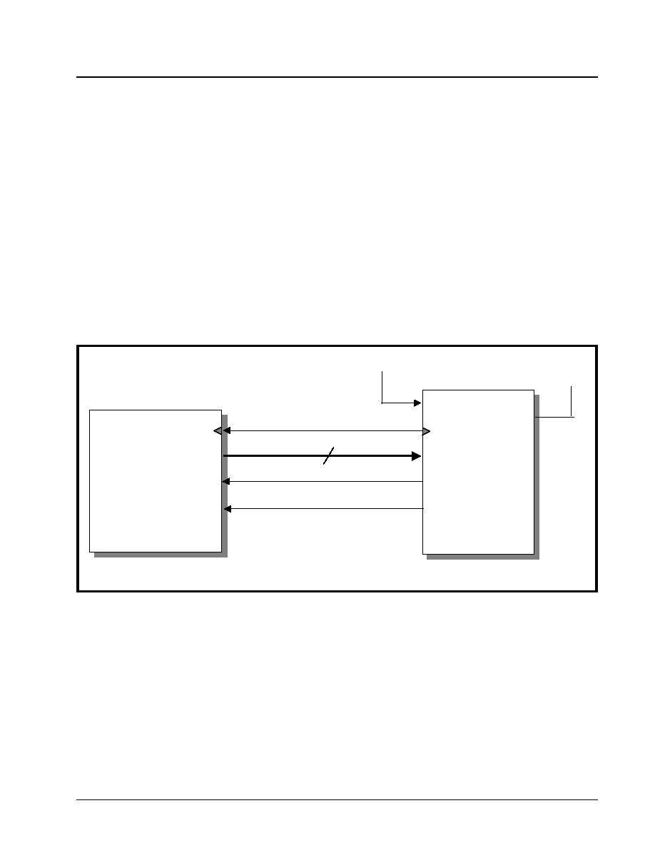
·Á
·Á
·Á
·Á
XRT7250
DS3/E3 FRAMER IC
REV. 1.1.1
251
B. Nibble-Parallel Mode
The XRT7250 will accept the E3 payload data, from
the Terminal Equipment, in a parallel manner, via the
TxNib[3:0] input pins. The Transmit Terminal Equip-
ment Input Interface will latch this data into its circuit-
ry, on the rising edge of the TxNibClk output signal.
C. Delineation of outbound E3 Frames
The Transmit Section will use the TxInClk input signal
as its timing reference and will initiate the generation
of E3 frames, asynchronous with respect to any ex-
ternal signal. The XRT7250 will pulse the TxFrame
output pin "High" whenever it is processing the last
bit, within a given outbound E3 frame.
D. Sampling of payload data, from the Terminal
Equipment
In Mode 6, the XRT7250 will sample the data, at the
TxNib[3:0] input pins, on the third rising edge of the
TxInClk clock signal, following a pulse in the TxNibClk
signal (see Figure 111).
N
OTE
: The TxNibClk signal, from the XRT7250 operates
nominally at 8.592 MHz (e.g., 34.368 MHz divided by 4).
Interfacing the Transmit Payload Data Input Inter-
face block of the XRT7250 to the Terminal Equip-
ment for Mode 6 Operation
Figure 110 presents an illustration of the Transmit
Payload Data Input Interface block (within the
XRT7250) being interfaced to the Terminal Equip-
ment, for Mode 6 Operation.
Mode 6 Operation of the Terminal Equipment
In Figure 110 both the Terminal Equipment and the
XRT7250 will be driven by an external 8.592MHz
clock signal. The Terminal Equipment will receive the
8.592MHz clock signal via the E3_Nib_Clock_In input
pin. The XRT7250 will output the 8.592MHz clock
signal via the TxNibClk output pin.
The Terminal Equipment will serially output the data
on the E3_Data_Out[3:0] pins upon the rising edge of
the signal at the E3_Clock_In input pin. The
XRT7250 will latch the data, residing on the Tx-
Nib[3:0] input pins, on the rising edge of the TxNibClk
signal.
In this case the XRT7250 has the responsibility of
providing the framing reference signal by pulsing the
TxFrame output pin (and in turn the
Tx_Start_of_Frame input pin of the Terminal Equip-
ment) "High" for one bit-period, coincident with the
last bit within a given E3 frame.
Finally, the XRT7250 will always internally generate
the Overhead bits, when it is operating in both the E3
and Nibble-parallel modes. The XRT7250 will pull the
TxOHInd input pin "Low".
The behavior of the signals between the XRT7250
and the Terminal Equipment for E3 Mode 6 Operation
is illustrated in Figure 111.
F
IGURE
110. I
LLUSTRATION
OF
THE
T
ERMINAL
E
QUIPMENT
BEING
INTERFACED
TO
THE
T
RANSMIT
P
AYLOAD
D
ATA
I
NPUT
I
NTERFACE
BLOCK
OF
THE
XRT7250
FOR
M
ODE
6 (N
IBBLE
-P
ARALLEL
/L
OCAL
-T
IMED
/F
RAME
-M
ASTER
)
O
PERATION
Terminal Equipment
XRT7250 E3 Framer
E3_Data_Out[3:0]
E3_Nib_Clock_In
Tx_Start_of_Frame
TxNib[3:0]
TxNibClk
TxNibFrame
NibInt
VCC
4
34.368MHz Clock Source
TxInClk
8.592MHz
TxOH_Ind
E3_Overhead_Ind
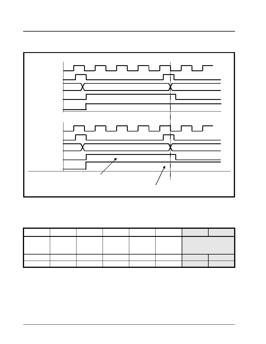
XRT7250
·Á
·Á
·Á
·Á
DS3/E3 FRAMER IC
REV. 1.1.1
252
How to configure the XRT7250 into Mode 6
1. Set the NibInt input pin "High".
2. Set the TimRefSel[1:0] bit-fields (within the
Framer Operating Mode Register) to "1X" as illus-
trated below.
3. Interface the XRT7250, to the Terminal Equip-
ment, as illustrated in Figure 110.
5.2.2
The Transmit Overhead Data Input Inter-
face
Figure 112 presents a simple illustration of the Trans-
mit Overhead Data Input Interface block within the
XRT7250.
F
IGURE
111. B
EHAVIOR
OF
THE
T
ERMINAL
I
NTERFACE
SIGNALS
BETWEEN
THE
XRT7250
AND
THE
T
ERMINAL
E
QUIPMENT
(E3 M
ODE
6 O
PERATION
)
Terminal Equipment Signals
TxInClk
Tx_Start_of_Frame
E3_Nib_Clock_In
E3_Data_Out[3:0]
Payload Nibble [380]
Overhead Nibble [0]
XRT7250 Transmit Payload Data I/F Signals
E3 Frame Number N
E3 Frame Number N + 1
Note: TxNibFrame pulses high to denote
E3 Frame Boundary.
TxInClk
TxNibFrame
TxNibClk
TxNib[3:0]
Nibble [380]
Overhead Nibble [0]
E3_Overhead_Ind
TxOH_Ind
TxOH_Ind pulses high for 3 Nibble periods
FRAMER OPERATING MODE REGISTER (ADDRESS = 0X00)
B
IT
7
B
IT
6
B
IT
5
B
IT
4
B
IT
3
B
IT
2
B
IT
1
B
IT
0
Local
Loopback
DS3/E3*
Internal
LOS
Enable
RESET
Interrupt
Enable
Reset
Frame
Format
TimRefSel[1:0]
R/W
R/W
R/W
R/W
R/W
R/W
R/W
R/W
0
0
1
0
1
0
1
x
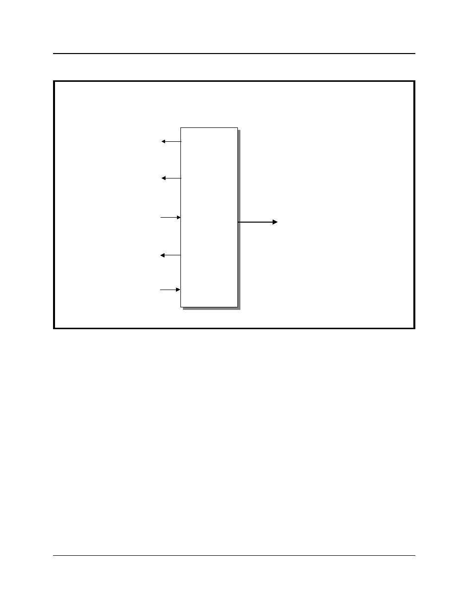
·Á
·Á
·Á
·Á
XRT7250
DS3/E3 FRAMER IC
REV. 1.1.1
253
The E3, ITU-T G.751 Frame consists of 1536 bits. Of
these bits, 1524 are payload bits and the remaining
12 are overhead bits. The XRT7250 has been de-
signed to handle and process both the payload type
and overhead type bits for each E3 frame. Within the
Transmit Section within the XRT7250, the Transmit
Payload Data Input Interface has been designed to
handle the payload data. Likewise, the Transmit
Overhead Input Interface has been designed to han-
dle and process the overhead bits.
The Transmit Section of the XRT7250 generates or
processes the various overhead bits within the E3
frame, in the following manner.
The Frame Alignment Signaling (FAS) Overhead
Bits
The FAS (Framing Alignment Signaling) bits are al-
ways internally generated by the Transmit Section of
the XRT7250. Hence, the user cannot insert his/her
value for the FAS bits into the outbound E3 data
stream, via the Transmit Overhead Data Input Inter-
face.
The "A" (Alarm) Overhead bit
The "A" bit is used to transport the FERF (Far-End
Receive Failure) condition. This bit-field can be either
internally generated by the Transmit Section within
the XRT7250, or can be externally generated and in-
serted into the outbound E3 data stream, via the
Transmit Overhead Data Input Interface. The Data
Link Related Overhead Bits
The "N" (National) Overhead bit
The E3 frame structure also contains the N bit which
can be used to transport a proprietary User Data Link
information and or Path Maintenance Data Link infor-
mation. The UDL (User Data Link) bits are only ac-
cessible via the Transmit Overhead Data Input Inter-
face. The Path Maintenance Data Link (PMDL) bits
can either be sourced from the Transmit LAPD Con-
troller/Buffer or via the Transmit Overhead Data Input
Interface.
Table 47 lists the Overhead Bits within the E3 frame.
In addition, this table also indicates whether or not
these overhead bits can be sourced by the Transmit
Overhead Data Input Interface.
F
IGURE
112. S
IMPLE
I
LLUSTRATION
OF
THE
T
RANSMIT
O
VERHEAD
D
ATA
I
NPUT
I
NTERFACE
BLOCK
Transmit
Overhead
Data Input
Interface Block
Transmit
Overhead
Data Input
Interface Block
TxOHFrame
TxOHEnable
TxOH
TxOHClk
TxOHIns
To Transmit DS3 Framer Block

XRT7250
·Á
·Á
·Á
·Á
DS3/E3 FRAMER IC
REV. 1.1.1
254
N
OTES
:
1. The XRT7250 contains mask register bits that per-
mit the user to alter the state of the internally gen-
erated value for these bits.
2. The Transmit LAPD Controller/Buffer can be config-
ured to be the source of the N bits, within the out-
bound E3 data stream.
The Transmit Overhead Data Input Interface permits
the user to insert overhead data into the outbound E3
frames via the following two different methods.
∑ Method 1 - Using the TxOHClk clock signal
∑ Method 2 - Using the TxInClk and the TxOHEnable
signals.
Each of these methods are described below.
5.2.2.1
Method 1 - Using the TxOHClk Clock
Signal
The Transmit Overhead Data Input Interface consists
of the five signals. Of these five (5) signals, the fol-
lowing four (4) signals are to be used when imple-
menting Method 1.
∑ TxOH
∑ TxOHClk
∑ TxOHFrame
∑ TxOHIns
Each of these signals are listed and described below.
Table 48.
T
ABLE
47: A L
ISTING
OF
THE
O
VERHEAD
BITS
WITHIN
THE
E3
FRAME
,
AND
THEIR
POTENTIAL
SOURCES
,
WITHIN
THE
XRT7250 IC
O
VERHEAD
B
IT
I
NTERNALLY
GENERATED
A
CCESSIBLE
VIA
THE
T
RANSMIT
O
VERHEAD
D
ATA
I
NPUT
I
NTERFACE
B
UFFER
/R
EGISTER
A
CCESSIBLE
FAS Signal - Bit 9
Yes
Yes
Yes*
FAS Signal - Bit 8
Yes
Yes
Yes
FAS Signal - Bit 7
Yes
Yes
Yes*
FAS Signal - Bit 6
Yes
Yes
Yes*
FAS Signal - Bit 5
Yes
Yes
Yes
FAS Signal - Bit 4
Yes
Yes
Yes
FAS Signal - Bit 3
Yes
Yes
Yes
FAS Signal - Bit 2
Yes
Yes
Yes
FAS Signal - Bit 1
Yes
Yes
Yes
FAS Signal - Bit 0
Yes
Yes
Yes
A Bit
Yes
Yes
Yes
N Bit
Yes
Yes
Yes

·Á
·Á
·Á
·Á
XRT7250
DS3/E3 FRAMER IC
REV. 1.1.1
255
Interfacing the Transmit Overhead Data Input In-
terface to the Terminal Equipment.
Figure 113 illustrates how one should interface the
Transmit Overhead Data Input Interface to the Termi-
nal Equipment, when using Method 1.
T
ABLE
48: D
ESCRIPTION
OF
M
ETHOD
1 T
RANSMIT
O
VERHEAD
I
NPUT
I
NTERFACE
S
IGNALS
N
AME
T
YPE
D
ESCRIPTION
TxOHIns
Input
Transmit Overhead Data Insert Enable input pin.
Asserting this input signal (e.g., setting it "High") enables the Transmit Overhead Data Input Inter-
face to accept overhead data from the Terminal Equipment. In other words, while this input pin is
"High", the Transmit Overhead Data Input Interface will sample the data at the TxOH input pin, on
the falling edge of the TxOHClk output signal.
Conversely, setting this pin "Low" configures the Transmit Overhead Data Input Interface to NOT
sample (e.g., ignore) the data at the TxOH input pin, on the falling edge of the TxOHClk output
signal.
N
OTE
: If the Terminal Equipment attempts to insert an overhead bit that cannot be accepted by
the Transmit Overhead Data Input Interface (e.g., if the Terminal Equipment asserts the TxOHIns
signal, at a time when one of these non-insertable overhead bits are being processed), that par-
ticular insertion effort will be ignored.
TxOH
Input
Transmit Overhead Data Input pin:
The Transmit Overhead Data Input Interface accepts the overhead data via this input
pin, and inserts into the overhead bit position within the very next outbound E3 frame. If
the TxOHIns pin is pulled "High", the Transmit Overhead Data Input Interface will sam-
ple the data at this input pin (TxOH), on the falling edge of the TxOHClk output pin.
Conversely, if the TxOHIns pin is pulled "Low", then the Transmit Overhead Data Input
Interface will NOT sample the data at this input pin (TxOH). Consequently, this data will
be ignored.
TxOHClk
Output
Transmit Overhead Input Interface Clock Output signal:
This output signal serves two purposes:
1. The Transmit Overhead Data Input Interface will provide a rising clock edge on this signal, one
bit-period prior to the instant that the Transmit Overhead Data Input Interface is processing an
overhead bit.
2. The Transmit Overhead Data Input Interface will sample the data at the TxOH input, on the fall-
ing edge of this clock signal (provided that the TxOHIns input pin is "High").
N
OTE
: The Transmit Overhead Data Input Interface will supply a clock edge for all overhead bits
within the DS3 frame (via the TxOHClk output signal). This includes those overhead bits that the
Transmit Overhead Data Input Interface will not accept from the Terminal Equipment.
TxOHFrame
Output
Transmit Overhead Input Interface Frame Boundary Indicator Output:
This output signal pulses "High" when the XRT7250 is processing the last bit within a
given E3 frame.
The purpose of this output signal is to alert the Terminal Equipment that the Transmit
Overhead Data Input Interface block is about to begin processing the overhead bits for a
new E3 frame.
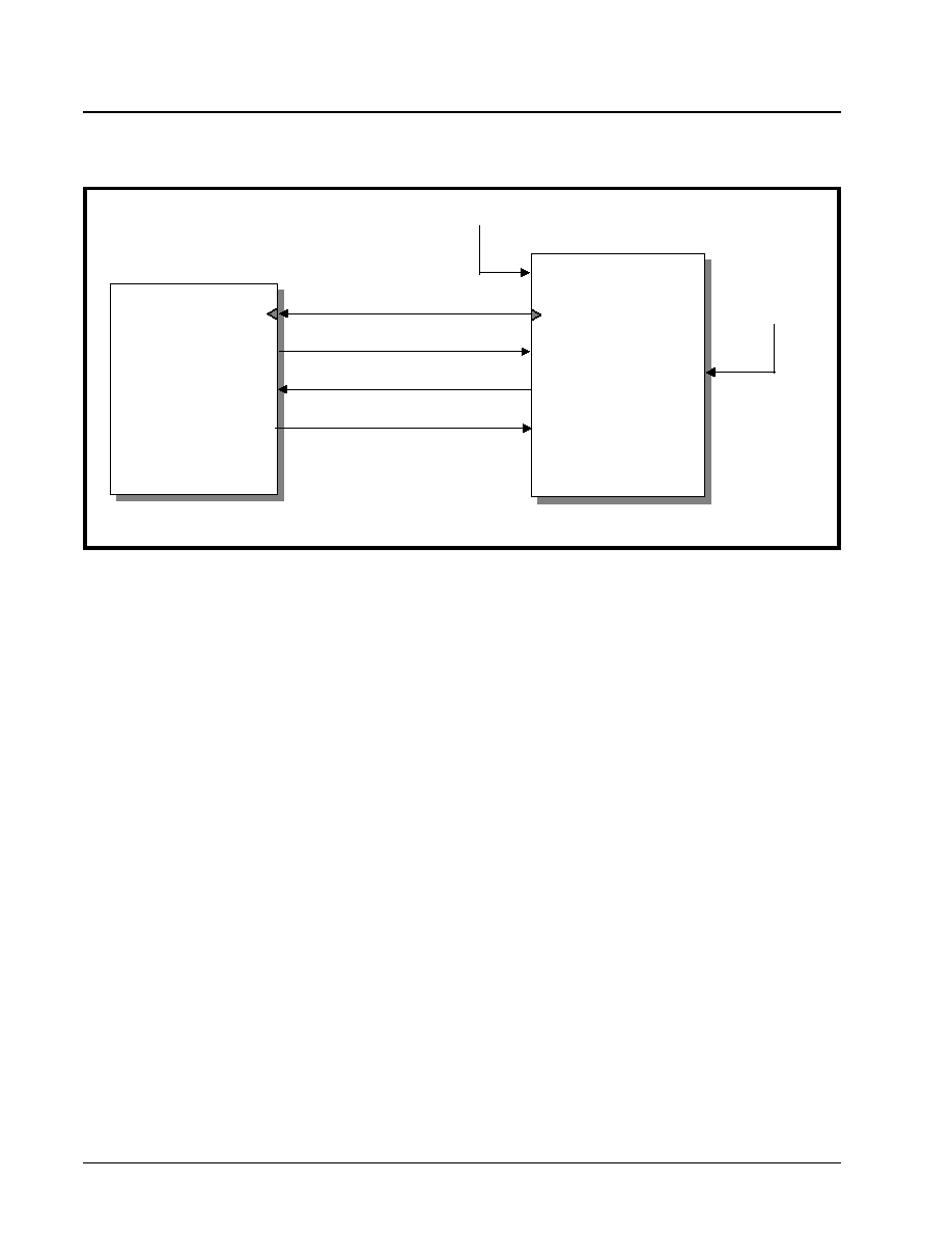
XRT7250
·Á
·Á
·Á
·Á
DS3/E3 FRAMER IC
REV. 1.1.1
256
Method 1 Operation of the Terminal Equipment
If the Terminal Equipment intends to insert any over-
head data into the outbound E3 data stream, (via the
Transmit Overhead Data Input Interface), then it is ex-
pected to do the following.
1. To sample the state of the TxOHFrame signal
(e.g., the Tx_Start_of_Frame input signal) on the
rising edge of the TxOHClk (e.g., the
E3_OH_Clock_In signal).
2. To keep track of the number of rising clock edges
that have occurred, via the TxOHClk (e.g., the
E3_OH_Clock_In signal) since the last time the
TxOHFrame signal was sampled "High". By
doing this the Terminal Equipment will be able to
keep track of which overhead bit is being pro-
cessed by the Transmit Overhead Data Input
Interface block at any given time. When the Ter-
minal Equipment knows which overhead bit is
being processed, at a given TxOHClk period, it
will know when to insert a desired overhead bit
value into the outbound E3 data stream. From
this, the Terminal Equipment will know when it
should assert the TxOHIns input pin and place
the appropriate value on the TxOH input pin (of
the XRT7250).
Table 49 relates the number of rising clock edges (in
the TxOHClk signal, since TxOHFrame was sampled
"High") to the E3 Overhead Bit, that is being pro-
cessed.
F
IGURE
113. I
LLUSTRATION
OF
THE
T
ERMINAL
E
QUIPMENT
BEING
INTERFACED
TO
THE
T
RANSMIT
O
VERHEAD
D
ATA
I
NPUT
I
NTERFACE
(M
ETHOD
1)
Terminal Equipment
XRT7250 E3 Framer
E3_OH_Out]
E3_OH_Clock_In
Tx_Start_of_Frame
TxOHClk
TxOHFrame
TxOHIns
34.368 MHz Clock Source
TxInClk
TxOH
Insert_OH
RxLineClk
34.368 MHz
Clock Source

·Á
·Á
·Á
·Á
XRT7250
DS3/E3 FRAMER IC
REV. 1.1.1
257
3. After the Terminal Equipment has waited the
appropriate number of clock edges (from the
TxOHFrame signal being sampled "High"), it
should assert the TxOHIns input signal. Concur-
rently, the Terminal Equipment should also place
the appropriate value (of the inserted overhead
bit) onto the TxOH signal.
4. The Terminal Equipment should hold both the
TxOHIns input pin "High" and the value of the
TxOH signal, stable until the next rising edge of
TxOHClk is detected.
Case Study: The Terminal Equipment intends to
insert the appropriate overhead bits into the
Transmit Overhead Data Input Interface (using
Method 1) in order to transmit a Yellow Alarm to
the remote terminal equipment.
In this example, the Terminal Equipment intends to in-
sert the appropriate overhead bits, into the Transmit
Overhead Data Input Interface, such that the
XRT7250 will transmit a Yellow Alarm to the remote
terminal equipment. Recall that, for E3, ITU-T G.751
Applications, a Yellow Alarm is transmitted by setting
the "A" bit to "1".
If one assumes that the connection between the Ter-
minal Equipment and the XRT7250 are as illustrated
in Figure 113 then Figure 114 presents an illustration
of the signaling that must go on between the Terminal
Equipment and the XRT7250.
T
ABLE
49: T
HE
R
ELATIONSHIP
BETWEEN
THE
N
UMBER
OF
R
ISING
C
LOCK
E
DGES
IN
T
X
OHC
LK
, (
SINCE
T
X
OHF
RAME
WAS
LAST
SAMPLED
"H
IGH
")
TO
THE
E3 O
VERHEAD
B
IT
,
THAT
IS
BEING
PROCESSED
N
UMBER
OF
R
ISING
C
LOCK
E
DGES
IN
T
X
OHC
LK
T
HE
O
VERHEAD
B
IT
E
XPECTED
BY
THE
XRT7250
C
AN
THIS
OVERHEAD
BIT
BE
ACCEPTED
BY
THE
XRT7250?
0 (Clock edge is coincident with TxO-
HFrame being detected "High")
FAS Signal - Bit 9
Yes
1
FAS Signal - Bit 8
Yes
2
FAS Signal - Bit 7
Yes
3
FAS Signal - Bit 6
Yes
4
FAS Signal - Bit 5
Yes
5
FAS Signal - Bit 4
Yes
6
FAS Signal - Bit 3
Yes
7
FAS Signal - Bit 2
Yes
8
FAS Signal - Bit 1
Yes
9
FAS Signal - Bit 0
Yes
10
A Bit
Yes
11
N Bit
Yes
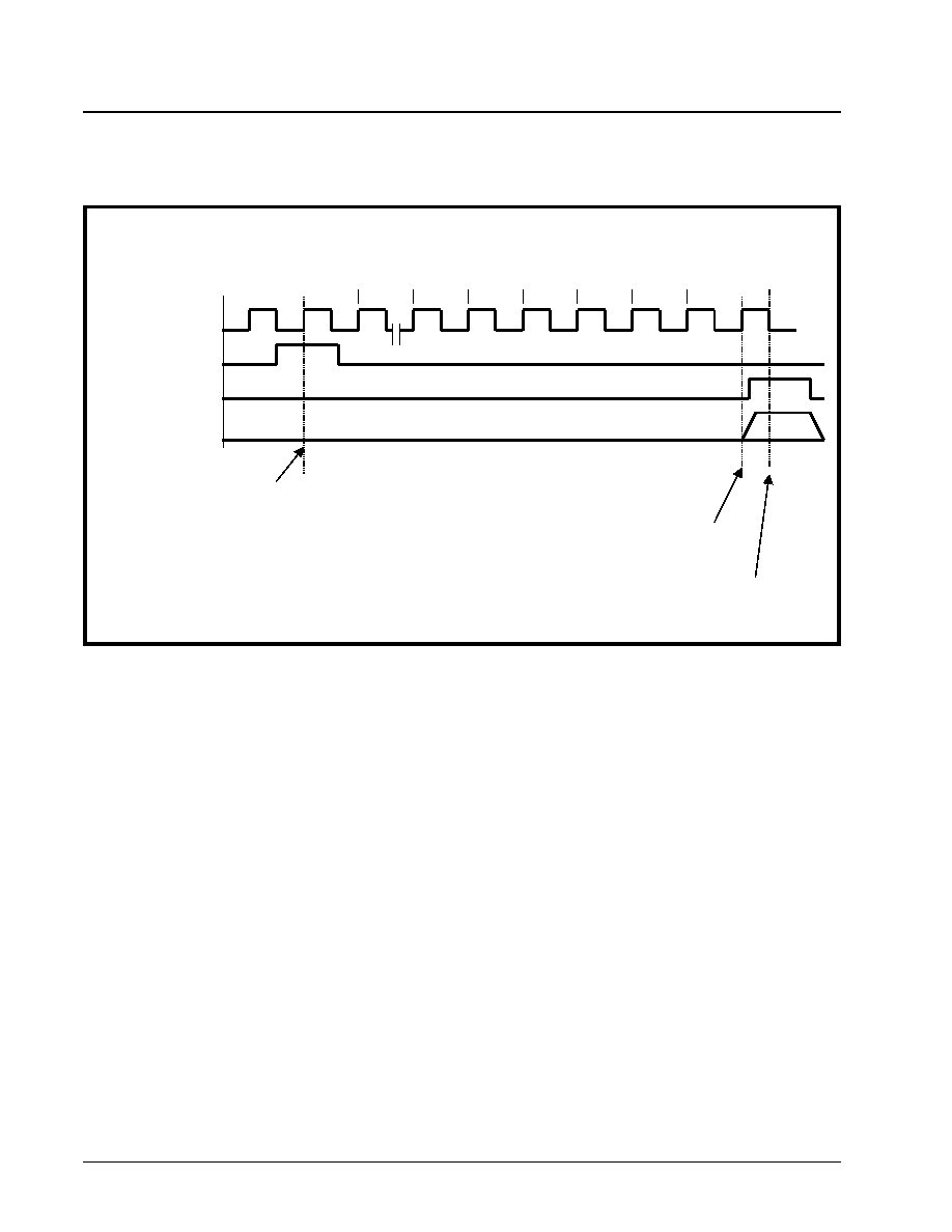
XRT7250
·Á
·Á
·Á
·Á
DS3/E3 FRAMER IC
REV. 1.1.1
258
In Figure 114 the Terminal Equipment samples the
TxOHFrame signal being "High" at rising clock edge #
0. From this point, the Terminal Equipment will wait
until it has detected the 10th rising edge of the TxO-
HClk signal. At this point, the Terminal Equipment
knows that the XRT7250 is just about to process the
"A" bit within a given outbound E3 frame. Additionally,
according to Table 49, the 10th overhead bit to be
processed is the "A" bit. In order to facilitate the
transmission of the Yellow Alarm, the Terminal Equip-
ment must set this "A" bit to "1". Hence, the Terminal
Equipment starts this process by implementing the
following steps concurrently.
a. Assert the TxOHIns input pin by setting it "High".
b. Set the TxOH input pin to "1".
After the Terminal Equipment has applied these sig-
nals, the XRT7250 will sample the data on both the
TxOHIns and TxOH signals upon the very next falling
edge of TxOHClk (designated as "10-" in Figure 114).
Once the XRT7250 has sampled this data, it will then
insert a "1" into the "A" bit position, in the outbound
E3 frame.
Upon detection of the very next rising edge of the Tx-
OHClk clock signal (designated as clock edge 1 in
Figure 114, the Terminal Equipment will negate the
TxOHIns signal (e.g., toggles it "Low") and will cease
inserting data into the Transmit Overhead Data Input
Interface.
After the Terminal Equipment has performed this in-
sertion procedure, it leaves the remaining overhead
bits (within this particular outbound E3 frame) in-tact,
by terminating this Overhead Bit Insertion proce-
dure. The Terminal Equipment should now terminate
this overhead bit insertion, by doing the following.
a. Assert the TxOHIns input pin by setting it "High".
b. Set the TxOH input to "0".
If the Terminal Equipment wishes to continue its
transmission of the Yellow Alarm condition to the Re-
mote Terminal Equipment, then it should resume the
Overhead Bit Insertion procedure (as described
above), at the beginning of each outbound E3 frame
(or each time TxOHFrame is sampled "High").
5.2.2.2
Method 2 - Using the TxInClk and TxO-
HEnable Signals
Method 1 requires the use of an additional clock sig-
nal, TxOHClk. However, there may be a situation in
which the user does not wish to add this extra clock
signal to their design, in order to use the Transmit
Overhead Data Input Interface. Hence, Method 2 is
F
IGURE
114. I
LLUSTRATION
OF
THE
SIGNAL
THAT
MUST
OCCUR
BETWEEN
THE
T
ERMINAL
E
QUIPMENT
AND
THE
XRT7250
IN
ORDER
TO
CONFIGURE
THE
XRT7250
TO
TRANSMIT
A
Y
ELLOW
A
LARM
TO
THE
REMOTE
TERMINAL
EQUIPMENT
Terminal Equipment/XRT7250 Interface Signals
TxOHClk
TxOHIns
TxOHFrame
TxOH
Remaining Overhead Bits with E3 Frame
A bit = 1
TxOHFrame is sampled "high"
Terminal Equipment asserts TxOHIns and
Data on TxOH line.
0 1 4 5 6 7 8 9 10 10-
XRT7250 Framer device samples TxOH and
TxOHIns signals

·Á
·Á
·Á
·Á
XRT7250
DS3/E3 FRAMER IC
REV. 1.1.1
259
available. When using Method 2, either the TxInClk
or RxOutClk signal is used to sample the overhead
bits and signals which are input to the Transmit Over-
head Data Input Interface. Method 2 involves the use
of the following signals:
∑ TxOH
∑ TxInClk
∑ TxOHFrame
∑ TxOHEnable
Each of these signals are listed and described in
Table 50.
Interfacing the Transmit Overhead Data Input Interface
to the Terminal Equipment
Figure 115 illustrates how one should interface the
Transmit Overhead Data Input Interface to the Termi-
nal Equipment when using Method 2.
T
ABLE
50: D
ESCRIPTION
OF
M
ETHOD
2 T
RANSMIT
O
VERHEAD
I
NPUT
I
NTERFACE
S
IGNALS
N
AME
T
YPE
D
ESCRIPTION
TxOHEn-
able
Output
Transmit Overhead Data Enable Output pin
The XRT7250 will assert this signal, for one TxInClk period, just prior to the instant that the
Transmit Overhead Data Input Interface is processing an overhead bit.
TxO-
HFrame
Output
Transmit Overhead Input Interface Frame Boundary Indicator Output:
This output signal pulses "High" when the XRT7250 is processing the last bit within a given DS3
frame.
TxOHIns
Input
Transmit Overhead Data Insert Enable input pin.
Asserting this input signal (e.g., setting it "High") enables the Transmit Overhead Data Input
Interface to accept overhead data from the Terminal Equipment. In other words, while this input
pin is "High", the Transmit Overhead Data Input Interface will sample the data at the TxOH input
pin, on the falling edge of the TxInClk output signal.
Conversely, setting this pin "Low" configures the Transmit Overhead Data Input Interface to NOT
sample (e.g., ignore) the data at the TxOH input pin, on the falling edge of the TxOHClk output
signal.
N
OTE
: If the Terminal Equipment attempts to insert an overhead bit that cannot be accepted by
the Transmit Overhead Data Input Interface (e.g., if the Terminal Equipment asserts the TxOHIns
signal, at a time when one of these non-insertable overhead bits are being processed), that par-
ticular insertion effort will be ignored.
TxOH
Input
Transmit Overhead Data Input pin:
The Transmit Overhead Data Input Interface accepts the overhead data via this input pin, and
inserts into the overhead bit position within the very next outbound DS3 frame. If the TxOHIns
pin is pulled "High", the Transmit Overhead Data Input Interface will sample the data at this input
pin (TxOH), on the falling edge of the TxOHClk output pin. Conversely, if the TxOHIns pin is
pulled "Low", then the Transmit Overhead Data Input Interface will NOT sample the data at this
input pin (TxOH). Consequently, this data will be ignored.

XRT7250
·Á
·Á
·Á
·Á
DS3/E3 FRAMER IC
REV. 1.1.1
260
Method 2 Operation of the Terminal Equipment
If the Terminal Equipment intends to insert any over-
head data into the outbound E3 data stream (via the
Transmit Overhead Data Input Interface), then it is ex-
pected to do the following.
1. To sample the state of both the TxOHFrame and
the TxOHEnable input signals, via the
E3_Clock_In (e.g., either the TxInClk or the
RxOutClk signal of the XRT7250) signal. If the
Terminal Equipment samples the TxOHEnable
signal "High", then it knows that the XRT7250 is
about to process an overhead bit. Further, if the
Terminal Equipment samples both the TxO-
HFrame and the TxOHEnable pins "High" (at the
same time) then the Terminal Equipment knows
that the XRT7250 is about to process the first
overhead bit, within a new E3 frame.
2. To keep track of the number of times that the
TxOHEnable signal has been sampled "High"
since the last time both the TxOHFrame and the
TxOHEnable signals were sampled "High". By
doing this, the Terminal Equipment will be able to
keep track of which overhead bit the Transmit
Overhead Data Input Interface is about ready to
process. From this, the Terminal Equipment will
know when it should assert the TxOHIns input pin
and place the appropriate value on the TxOH
input pins of the XRT7250.
Table 51 also relates the number of TxOHEnable out-
put pulses (that have occurred since both the TxO-
HFrame and TxOHEnable pins were sampled "High")
to the E3 overhead bit, that is being processed.
F
IGURE
115. I
LLUSTRATION
OF
THE
T
ERMINAL
E
QUIPMENT
BEING
INTERFACED
TO
THE
T
RANSMIT
O
VERHEAD
D
ATA
I
NPUT
I
NTERFACE
(M
ETHOD
2)
Terminal Equipment
XRT7250 E3 Framer
E3_OH_Out
E3_OH_Enable
Tx_Start_of_Frame
TxOHEnable
TxOHFrame
TxOHIns
34.368 MHz Clock Source
TxInClk
TxOH
Insert_OH
RxLineClk
34.368 MHz
Clock Source
E3_Clock_In

·Á
·Á
·Á
·Á
XRT7250
DS3/E3 FRAMER IC
REV. 1.1.1
261
3. After the Terminal Equipment has waited through
the appropriate number of pulses via the TxO-
HEnable pin, it should then assert the TxOHIns
input signal. Concurrently, the Terminal Equip-
ment should also place the appropriate value (of
the inserted overhead bit) onto the TxOH signal.
4. The Terminal Equipment should hold both the
TxOHIns input pin "High" and the value of the
TxOH signal stable, until the next TxOHEnable
pulse is detected.
Case Study: The Terminal Equipment intends to
insert the appropriate overhead bits into the
Transmit Overhead Data Input Interface (using
Method 2) in order to transmit a Yellow Alarm to
the remote terminal equipment.
In this case, the Terminal Equipment intends to insert
the appropriate overhead bits, into the Transmit Over-
head Data Input Interface such that the XRT7250 will
transmit a Yellow Alarm to the remote terminal equip-
ment. Recall that, for E3, ITU-T G.751 applications, a
Yellow Alarm is transmitted by setting the "A" bit to
"1".
If one assumes that the connection between the Ter-
minal Equipment and the XRT7250 is as illustrated in
Figure 115 then, Figure 116 presents an illustration of
the signaling that must go on between the Terminal
Equipment and the XRT7250.
T
ABLE
51: T
HE
R
ELATIONSHIP
BETWEEN
THE
N
UMBER
OF
T
X
OHE
NABLE
PULSES
(
SINCE
THE
LAST
OCCURRENCE
OF
THE
T
X
OHF
RAME
PULSE
)
TO
THE
E3 O
VERHEAD
B
IT
,
THAT
IS
BEING
PROCESSED
BY
THE
XRT7250
N
UMBER
OF
T
X
OHE
NABLE
P
ULSES
T
HE
O
VERHEAD
B
IT
E
XPECTED
BY
THE
XRT7250
C
AN
THIS
OVERHEAD
BIT
BE
ACCEPTED
BY
THE
XRT7250?
0 (Clock edge is coincident with TxO-
HFrame being detected "High")
FAS Signal - Bit 9
Yes
1
FAS Signal - Bit 8
Yes
2
FAS Signal - Bit 7
Yes
3
FAS Signal - Bit 6
Yes
4
FAS Signal - Bit 5
Yes
5
FAS Signal - Bit 4
Yes
6
FAS Signal - Bit 3
Yes
7
FAS Signal - Bit 2
Yes
8
FAS Signal - Bit 1
Yes
9
FAS Signal - Bit 0
Yes
10
A Bit
Yes
11
N Bit
Yes
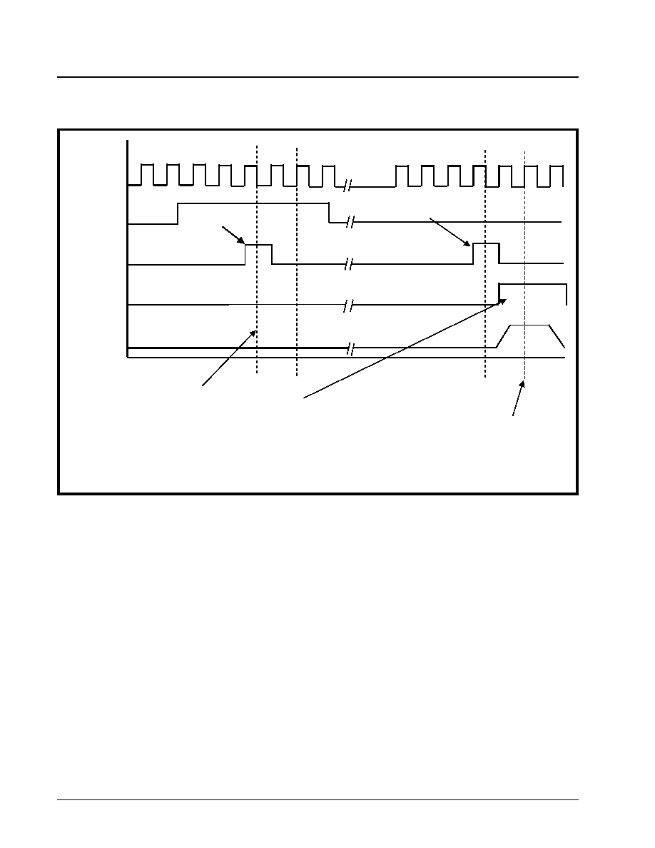
XRT7250
·Á
·Á
·Á
·Á
DS3/E3 FRAMER IC
REV. 1.1.1
262
5.2.3
The Transmit E3 HDLC Controller
The Transmit E3 HDLC Controller block can be used
to transport Message-Oriented Signaling (MOS) type
messages to the remote terminal equipment as dis-
cussed in detail below.
5.2.3.1
Message-Oriented Signaling (e.g.,
LAP-D) processing via the Transmit DS3 HDLC
Controller
The LAPD Transmitter (within the Transmit E3 HDLC
Controller Block) allows the user to transmit path
maintenance data link (PMDL) messages to the re-
mote terminal via the outbound E3 Frames. In this
case the message bits are inserted into and carried
by the "N" bit, within the outbound E3 frames. The
on-chip LAPD transmitter supports both the 76 byte
and 82 byte length message formats, and the Framer
IC allocates 88 bytes of on-chip RAM (e.g., the Trans-
mit LAPD Message buffer) to store the message to be
transmitted. The message format complies with ITU-
T Q.921 (LAP-D) protocol with different addresses
and is presented below in Figure 117 .
F
IGURE
116. B
EHAVIOR
OF
T
RANSMIT
O
VERHEAD
D
ATA
I
NPUT
I
NTERFACE
SIGNALS
BETWEEN
THE
XRT7250
AND
THE
T
ERMINAL
E
QUIPMENT
(
FOR
M
ETHOD
2)
TxInClk
TxOHFrame
TxOHEnable
TxOHIns
TxOH
Terminal Equipment
samples "TxOHFrame" and
"TxOHEnable" being "HIGH"
Terminal Equipment counts the number of
TxOHEnable pulses. At "pulse # 10" the Terminal
Equipment asserts the "TxOHIns" signal and places the
desired data on TxOH.
XRT7250 samples TxOH
here.
TxOHEnable Pulse # 10
A bit = 1
TxOHEnable Pulse # 0
·Á
·Á
·Á
·Á
XRT7250
DS3/E3 FRAMER IC
REV. 1.1.1
263
Where: Flag Sequence = 0x7E
SAPI + CR + EA = 0x3C or 0x3E
TEI + EA = 0x01
Control = 0x03
The following sections defines each of these bit/byte-
fields within the LAPD Message Frame Format.
Flag Sequence Byte
The Flag Sequence byte is of the value 0x7E, and is
used to denote the boundaries of the LAPD Message
Frame.
SAPI - Service Access Point Identifier
The SAPI bit-fields are assigned the value of
"001111b" or 15 (decimal).
TEI - Terminal Endpoint Identifier
The TEI bit-fields are assigned the value of 0x00.
The TEI field is used in N-ISDN systems to identify a
terminal out of multiple possible terminal. However,
since the Framer IC transmits data in a point-to-point
manner, the TEI value is unimportant.
Control
The Control identifies the type of frame being trans-
mitted. There are three general types of frame for-
mats: Information, Supervisory, and Unnumbered.
The Framer assigned the Control byte the value 03h.
Hence, the Framer will be transmitting and receiving
Unnumbered LAPD Message frames.
Information Payload
The Information Payload is the 76 bytes or 82 bytes of
data (e.g., the PMDL Message) that the user has writ-
ten into the on-chip Transmit LAPD Message buffer
(which is located at addresses 0x86 through 0xDD).
It is important to note that the user must write in a
specific octet value into the first byte position within
the Transmit LAPD Message buffer (located at Ad-
dress = 0x86, within the Framer). The value of this
octet depends upon the type of LAPD Message
frame/PMDL Message that the user wishes to trans-
mit. Table 52 presents a list of the various types of
LAPD Message frames/PMDL Messages that are
supported by the XRT7250 Framer device and the
corresponding octet value that the user must write in-
to the first octet position within the Transmit LAPD
Message buffer.
F
IGURE
117. LAPD M
ESSAGE
F
RAME
F
ORMAT
Flag Sequence (8 bits)
SAPI (6-bits)
C/R
EA
TEI (7 bits)
EA
Control (8-bits)
76 or 82 Bytes of Information (Payload)
FCS - MSB
FCS - LSB
Flag Sequence (8-bits)
T
ABLE
52: T
HE
LAPD M
ESSAGE
T
YPE
AND
THE
C
ORRESPONDING
VALUE
OF
THE
F
IRST
B
YTE
,
WITHIN
THE
I
NFORMATION
P
AYLOAD
LAPD M
ESSAGE
T
YPE
V
ALUE
OF
F
IRST
B
YTE
,
WITHIN
I
NFORMATION
P
AYLOAD
OF
M
ESSAGE
M
ESSAGE
S
IZE
CL Path Identification
0x38
76 bytes
IDLE Signal Identification
0x34
76 bytes
Test Signal Identification
0x32
76 bytes
ITU-T Path Identification
0x3F
82 bytes

XRT7250
·Á
·Á
·Á
·Á
DS3/E3 FRAMER IC
REV. 1.1.1
264
Frame Check Sequence Bytes
The 16 bit FCS (Frame Check Sequence) is calculat-
ed over the LAPD Message Header and Information
Payload bytes, by using the CRC-16 polynomial, x
16
+ x
12
+ x
5
+ 1.
Operation of the LAPD Transmitter
If the user wishes to transmit a message via the
LAPD Transmitter, the information portion (or the
body) of the message must be written into the Trans-
mit LAPD Message Buffer, which is located at 0x86
through 0xDD in on-chip RAM via the Microprocessor
Interface. Afterwards, the user must do five things:
1. Configure the source of the "N" bit (within each
outbound E3 frame, to be the LAPD Transmitter.
2. Specify the length of LAPD message to be trans-
mitted.
3. Specify whether the LAPD Transmitter should
transmit this LAPD Message frame only once, or
an indefinite number of times at One-Second
intervals.
4. Enable the LAPD Transmitter.
5. Initiate the Transmission of the PMDL Message.
Each of these steps will be discussed in detail.
STEP 1 - Configure the source of the "N" bit (with-
in each outbound E3 frame, to be the LAPD Trans-
mitter.
This is accomplished by writing the appropriate data
into the TxNSourceSel[1:0] bit-fields, within the TxE3
Configuration Register, as illustrated below.
Setting TxNSourceSel[1:0] to "10" configures the
Transmit E3 Framer block to use the LAPD Transmit-
ter as the data source for the "N" bits. Hence, the "N"
bit, (within each outbound E3 frame) is now carrying
LAPD Messages to the remote terminal equipment.
STEP 2 - Specify the type of LAPD Message frame
to be Transmitted (within the Transmit LAPD Mes-
sage Buffer)
The user must write in a specific octet value into the
first octet position within the Transmit LAPD Buffer
(e.g., at Address Location 0x86 within the Framer IC).
This octet is referred to as the LAPD Message Frame
ID octet. The value of this octet must correspond to
the type of LAPD Message frame that is desired to be
transmitted. This octet will ultimately be used by the
Remote Terminal Equipment in order to help it identify
the type of LAPD message frame that it is receiving.
Table 53 lists these octets and the corresponding
LAPD Message types.
STEP 3 - Write the PMDL Message into the re-
maining part of the Transmit LAPD Message Buff-
er.
The user must now write in his/her PMDL Message
into the remaining portion of the Transmit LAPD Mes-
sage buffer (e.g., addresses 0x87 through 0x135
within the Framer IC).
STEP 4 - Specifying the Length of the LAPD Mes-
sage
One of two different sizes of LAPD Messages can be
transmitted. This can be accomplished by writing the
appropriate data to bit 1 within the Tx E3 LAPD Con-
figuration Register. The bit-format of this register is
presented below.
TXE3 CONFIGURATION REGISTER (ADDRESS = 0X30)
B
IT
7
B
IT
6
B
IT
5
B
IT
4
B
IT
3
B
IT
2
B
IT
1
B
IT
0
Tx
BIP-4
Enable
TxASourceSel[1:0]
TxNSourceSel[1:0]
Tx AIS
Enable
Tx LOS
Enable
Tx FAS
Source
Select
R/W
R/W
R/W
R/W
R/W
R/W
R/W
R/W
0
0
0
0
0
0
0
0
TRANSMIT E3 LAPD CONFIGURATION REGISTER (ADDRESS = 0X33)
B
IT
7
B
IT
6
B
IT
5
B
IT
4
B
IT
3
B
IT
2
B
IT
1
B
IT
0
Not Used
Auto
Retransmit
Not Used
TxLAPD
Msg Length
TxLAPD
Enable
R/O
R/O
R/O
R/O
R/W
R/O
R/W
R/W
0
0
0
0
X
0
X
X

·Á
·Á
·Á
·Á
XRT7250
DS3/E3 FRAMER IC
REV. 1.1.1
265
The relationship between the contents of bit-fields 1
and the LAPD Message size is given in Table 53.
N
OTE
: The Message Type selected must correspond with
the contents of the first byte of the Information (Payload)
portion, as presented in Table 52.
STEP 5 - Specify whether the LAPD Transmitter
should transmit the LAPD Message frame only
once, or an indefinite number of times at one-sec-
ond intervals.
The Transmit E3 HDLC Control block allows the user
to configure the LAPD Transmitter to transmit this
LAPD Message frame only once, or an indefinite
number of times at one-second intervals. The user
implements this configuration by writing the appropri-
ate value into Bit 3 (Auto Retransmit) within the Tx E3
LAPD Configuration Register (Address = 0x33), as
depicted below.
)
If the user writes a "1" into this bit-field, then the
LAPD Transmitter will transmit the LAPD Message
frame repeatedly at one-second intervals until the
LAPD Transmitter is disabled.
If the user writes a "0" into this bit-field, then the
LAPD Transmitter will transmit the LAPD Message
frame only once. Afterwards, the LAPD Transmitter
will halt its transmission until the user invokes the
Transmit LAPD Message frame command, once
again.
STEP 5 - Enabling the LAPD Transmitter
Prior to the transmission of any data via the LAPD
Transmitter, the LAPD Transmitter must be enabled.
This is accomplished by writing a "1" to bit 0 (TxLAPD
Enable) of the Tx E3 LAPD Configuration Register, as
depicted below.
If the user writes a "0" into this bit-field, then the
LAPD Transmitter will be enabled, and the LAPD
Transmitter will immediately begin to transmit a con-
tinuous stream of Flag Sequence octets (0x7E), via
the "N" bit-field of each outbound E3 frame.
Conversely, if the user writes a "1" into this bit-field,
then the LAPD Transmitter will be disabled. The
Transmit E3 Framer block will automatically insert a
"1" into the "N" bit-field, within each outbound E3
frame. No transmission of PMDL data will occur.
STEP 7 - Initiate the Transmission
At this point, the user should have written the PMDL
message into the on-chip Transmit LAPD Message
buffer and the type of LAPD Message that is desired
to be transmitted should have been specified. Finally,
T
ABLE
53: R
ELATIONSHIP
BETWEEN
T
X
LAPD M
SG
L
ENGTH
AND
THE
LAPD M
ESSAGE
S
IZE
T
X
LAPD M
ESSAGE
L
ENGTH
LAPD M
ESSAGE
L
ENGTH
0
LAPD Message size is 76 bytes
1
LAPD Message size is 82 bytes
TXE3 LAPD CONFIGURATION REGISTER (ADDRESS = 0X33)
B
IT
7
B
IT
6
B
IT
5
B
IT
4
B
IT
3
B
IT
2
B
IT
1
B
IT
0
Not Used
Auto
Retransmit
Not Used
TxLAPD
Msg Length
TxLAPD
Enable
RO
RO
RO
RO
R/W
RO
R/W
R/W
0
0
0
0
1
0
0
0
TRANSMIT E3 LAPD CONFIGURATION REGISTER (ADDRESS = 0X33)
B
IT
7
B
IT
6
B
IT
5
B
IT
4
B
IT
3
B
IT
2
B
IT
1
B
IT
0
Not Used
Auto
Retransmit
Not Used
TxLAPD
Msg Length
TxLAPD
Enable
R/O
R/O
R/O
E/O
R/W
R/O
R/W
R/W
0
0
0
0
X
0
X
1

XRT7250
·Á
·Á
·Á
·Á
DS3/E3 FRAMER IC
REV. 1.1.1
266
the user should have enabled the LAPD Transmitter.
The only remaining to do is initiate the transmission of
this message. This process is initiated by writing a
"1" to Bit 3 (Tx DL Start) within the Tx E3 LAPD Sta-
tus and Interrupt Register (Address = 0x34), as de-
picted below.
)
A "0" to "1" transition in Bit 3 (Tx DL Start) in this reg-
ister, initiates the transmission of LAPD Message
frames. At this point, the LAPD Transmitter will begin
to search through the PMDL message, which is resid-
ing within the Transmit LAPD Message buffer. If the
LAPD Transmitter finds any string of five (5) consecu-
tive "1's" in the PMDL Message then the LAPD Trans-
mitter will insert a "0" immediately following these
strings of consecutive "1's". This procedure is known
as stuffing. The purpose of PMDL Message stuffing
is to insure that the user's PMDL Message does not
contain strings of data that mimic the Flag Sequence
octet (e.g., six consecutive "1's") or the ABORT Se-
quence octet (e.g., seven consecutive "1's"). After-
wards, the LAPD Transmitter will begin to encapsu-
late the PMDL Message, residing in the Transmit
LAPD Message buffer, into a LAPD Message frame.
Finally, the LAPD Transmitter will fragment the out-
bound LAPD Message frame into bits and will begin
to transport these bits via the N bit-field within each
outbound E3 frame.
While the LAPD Transmitter is transmitting this LAPD
Message frame, the TxDL Busy bit-field (Bit 2) within
the Tx E3 LAPD Status and Interrupt Register, will be
set to "1". This bit-field allows the user to poll the sta-
tus of the LAPD Transmitter. Once the LAPD Trans-
mitter has completed the transmission of the LAPD
Message, then this bit-field will toggle back to "0".
The user can configure the LAPD Transmitter to inter-
rupt the local Microprocessor/Microcontroller upon
completion of transmission of the LAPD Message
frame, by setting bit-field "1" (TxLAPD Interrupt En-
able) within the Tx E3 LAPD Status and Interrupt reg-
ister (Address = 0x34). to "1" as depicted below.
)
`The purpose of t his interrupt is to let the Micropro-
cessor/Microcontroller know that the LAPD Transmit-
ter is available and ready to transmit a LAPD Mes-
sage frame (which contains a new PMDL Message)
to the remote terminal equipment. Bit 0 (Tx LAPD In-
terrupt Status) within the Tx E3 LAPD Status and In-
terrupt Register will reflect the status for the Transmit
LAPD Interrupt.
N
OTE
: This bit-field will be reset upon reading this register.
Summary of Operating the LAPD Transmitter
Once the user has invoked the TxDL Start command,
the LAPD Transmitter will do the following.
∑ Generate the four octets of the LAPD Message
frame header (e.g., the Flag Sequence, SAPI, TEI,
Control, etc.,) and insert them into the header byte
positions within the LAPD Message frame.
∑ It will read in the contents of the Transmit LAPD
Message buffer (e.g., the PMDL Message data)
and insert it into the Information Payload portion of
the LAPD Message frame.
TXE3 LAPD STATUS AND INTERRUPT REGISTER (ADDRESS = 0X34)
B
IT
7
B
IT
6
B
IT
5
B
IT
4
B
IT
3
B
IT
2
B
IT
1
B
IT
0
Not Used
TxDL Start
TxDL Busy
TxLAPD
Interrupt
Enable
TxLAPD
Interrupt
Status
RO
RO
RO
RO
R/W
RO
R/W
RUR
0
0
0
0
0
0
0
0
TXE3 LAPD STATUS AND INTERRUPT REGISTER (ADDRESS = 0X34)
B
IT
7
B
IT
6
B
IT
5
B
IT
4
B
IT
3
B
IT
2
B
IT
1
B
IT
0
Not Used
TxDL Start
TxDL Busy
TxLAPD
Interrupt
Enable
TxLAPD
Interrupt
Status
RO
RO
RO
RO
R/W
RO
R/W
RUR
0
0
0
0
X
X
1
X

·Á
·Á
·Á
·Á
XRT7250
DS3/E3 FRAMER IC
REV. 1.1.1
267
∑ Compute the 16-bit Frame Check Sequence (FCS)
value of the LAPD Message frame (e.g, of the
LAPD Message header and Payload bytes) and
insert this value into the FCS value octet positions
within the LAPD Message frame.
∑ Append a trailer Flag Sequence octet to the end of
the LAPD Message frame (following the 16-bit FCS
octets).
∑ Fragment the resulting LAPD Message frame into
bits and begin inserting these bits into the "N" bit-
field within each outbound E3 frame.
∑ Complete the transmission of the overhead bytes,
information payload byte, FCS value, and the trail-
ing Flag Sequence octets via the Transmit E3
Framer block.
Once the LAPD Transmitter has completed its trans-
mission of the LAPD Message frame, the Framer will
generate an Interrupt to the MIcroprocessor/Micro-
controller (if enabled). Afterwards, the LAPD Trans-
mitter will either halt its transmission of LAPD Mes-
sage frames or will proceed to retransmit the LAPD
Message frame, repeatedly at one-second intervals.
In between these transmissions of the LAPD Mes-
sage frames, the LAPD Transmitter will be sending a
continuous stream of Flag Sequence bytes. The
LAPD Transmitter will continue this behavior until the
user has disabled the LAPD Transmitter by writing a
"1" into bit 3 (No Data Link) within the Tx E3 Configu-
ration register.
N
OTE
: In order to prevent the user's data (e.g., the PMDL
Message within the LAPD Message frame) from mimicking
the Flag Sequence byte or an ABORT Sequence, the LAPD
Transmitter will parse through the PMDL Message data and
insert a "0" into this data, immediately following the detec-
tion of five (5) consecutive "1's" (this stuffing occurs while
the PMDL message data is being read in from the Transmit
LAPD Message frame. The Remote LAPD Receive (See
Section 4.3.5) will have the responsibility of checking the
newly received PMDL messages for a string of five (5) con-
secutive "1's" and removing the subsequent "0" from the
payload portion of the incoming LAPD Message.
Figure 118 presents a flow chart diagram.
Figure 118 depicts the procedure (in white boxes)
that the user should use in order to transmit a PMDL
message via the LAPD Transmitter, when the LAPD
Transmitter is configured to retransmit the LAPD Mes-
sage frame, repeatedly at One-Second intervals.
This figure also indicates (via the Shaded boxes)
what the LAPD Transmitter circuitry will do before and
during message transmission.
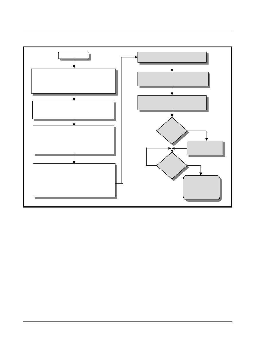
XRT7250
·Á
·Á
·Á
·Á
DS3/E3 FRAMER IC
REV. 1.1.1
268
N
OTE
: In Figure 118, the unshaded boxes depict the tasks
that the user must perform. The shaded boxes present the
resulting tasks that the Transmit HDLC Controller block will
perform.
The Mechanics of Transmitting a New LAPD Mes-
sage frame, if the LAPD Transmitter has been
configured to re-transmit the LAPD Message
frame, repeatedly, at One-Second intervals.
If the LAPD Transmitter has been configured to re-
transmit the LAPD Message frame repeatedly at one-
second intervals, then it will do the following (at one-
second intervals).
∑ Stuff the PMDL Message.
∑ Read in the stuffed PMDL Message from the Trans-
mit LAPD Message buffer.
∑ Encapsulate this stuffed PMDL Message into a
LAPD Message frame.
∑ Transmit this LAPD Message frame to the Remote
Terminal Equipment.
If another (e.g., a different) PMDL Message is to be
transmitted to the Remote Terminal Equipment, this
new message will have to be written into the Transmit
LAPD Message buffer, via the Microprocessor Inter-
face block of the Framer IC. However, care must be
taken when writing this new PMDL message. If this
message is written into the Transmit LAPD Message
buffer at the wrong time (with respect to these One-
second LAPD Message frame transmissions), the us-
er's action could interfere with these transmissions,
thereby causing the LAPD Transmitter to transmit a
corrupted message to the Remote Terminal Equip-
ment. In order to avoid this problem, while writing the
new message into the Transmit LAPD Message buff-
er, the user should do the following.
1. Configure the Framer to automatically reset acti-
vated interrupts.
The user can do this by writing a "1" into Bit 3 within
the Framer Operating Mode register (Address =
0x00), as depicted below.
F
IGURE
118. F
LOW
C
HART
D
EPICTING
HOW
TO
USE
THE
LAPD T
RANSMITTER
START
START
WRITE IN DATA LINK INFORMATION
The user accomplishes this by writing the information
that he/she wishes to transmit (via the LAPD
Transmitter) to locations 0x86through 0xDD, within the
Framer Address Space.
ENABLE THE LAPD
TRANSMITTER FOR TRANSMISSION
This is accomplished by writing 00000xx1bto the Tx
E3 LAPD Configuration Register.(where xx dictates
LAPD Message Type)
LAPD Transmitter inserts Frame Header
octets in front of the user payload.
LAPD Transmitter computes the 16 bit FCS
(a CRC-16 value) and inserts it into the LAPD
Message, following the user payload
LAPD Transmitter appends a Flag Sequence
Trailer octet to the end of the LAPD Message
(after the 16 bit FCS).
Is
5 consecutive
"1s" detected
?
Is
Message
Transmission
Complete
?
Insert a "0" after the
string of 5 consecutive
"1s"
END
Generate Interrupt
LAPD Transmitter will
continue to transmit
Flag Sequence octets.
INITIATE TRANSMISSION OF LAPD
MESSAGE
This is accomplished by writing 000010x0bto the Tx
E3 LAPD Status/InterruptRegister. (where x indicates
the user's choiceto enable/disable "LAPD Message
Transfer Complete" Interrupt
Yes
No
Yes
No
CONFIGURE THE N-BIT to CARRYLAPD
Messages
This is accomplished by setting "TxNSourceSel[1:0]
= "1, 0"

·Á
·Á
·Á
·Á
XRT7250
DS3/E3 FRAMER IC
REV. 1.1.1
269
This action will prevent the LAPD Transmitter from
generating its own One-Second interrupt (following
each transmission of the LAPD Message frame).
2. Enable the One-Second Interrupt
This can be done by writing a "1" into Bit 0 (One-Sec-
ond Interrupt Enable) within the Block Interrupt En-
able Register, as depicted below.
3. Write the new message into the Transmit LAPD
Message buffer immediately after the occurrence
of the One-Second Interrupt
By synchronizing the writes to the Transmit LAPD
Message buffer to occur immediately after the occur-
rence of the One-Second Interrupt, the user avoids
conflicting with the One-Second transmission of the
LAPD Message frame, and will transmit the correct
(uncorrupted) PMDL Message to the Remote LAPD
Receiver.
FRAMER OPERATING MODE REGISTER (ADDRESS = 0X00)
B
IT
7
B
IT
6
B
IT
5
B
IT
4
B
IT
3
B
IT
2
B
IT
1
B
IT
0
Local Loopback
DS3/E3*
Internal
LOS
Enable
RESET
Interrupt
Enable Reset
Frame Format
TimRefSel[1:0]
R/W
R/W
R/W
R/W
R/W
R/W
R/W
R/W
0
0
1
0
1
0
1
1
BLOCK INTERRUPT ENABLE REGISTER (ADDRESS = 0X04)
B
IT
7
B
IT
6
B
IT
5
B
IT
4
B
IT
3
B
IT
2
B
IT
1
B
IT
0
RxDS3/E3
Interrupt
Enable
Not Used
TxDS3/E3
Interrupt
Enable
One-Second
Interrupt
Enable
R/W
RO
RO
RO
RO
RO
R/W
R/W
0
0
0
0
0
0
0
0

XRT7250
·Á
·Á
·Á
·Á
DS3/E3 FRAMER IC
REV. 1.1.1
270
5.2.4
The Transmit E3 Framer Block
5.2.4.1
Brief Description of the Transmit E3
Framer
The Transmit E3 Framer block accepts data from any
of the following four sources, and uses it to form the
E3 data stream.
∑ The Transmit Payload Data Input block
∑ The Transmit Overhead Data Input block
∑ The Transmit HDLC Controller block
∑ The Internal Overhead Data Generator
The manner in how the Transmit E3 Framer block
handles data from each of these sources is described
below.
Handling of data from the Transmit Payload Data
Input Interface
For E3 applications, all data that is input to the Trans-
mit Payload Data Input Interface will be inserted into
the payload bit positions within the outbound E3
frames.
Handling of data from the Internal Overhead Bit
Generator
By default, the Transmit E3 Framer block will internal-
ly generate the overhead bytes. However, if the Ter-
minal Equipment inserts its own values for the over-
head bits or bytes (via the Transmit Overhead Data
Input Interface) or if the user enables and employs
the Transmit E3 HDLC Controller block, then these in-
ternally generated overhead bytes will be overwritten.
Handling of data from the Transmit Overhead Da-
ta Input Interface
For E3 applications, the Transmit E3 Framer block au-
tomatically generates and inserts the framing align-
ment bytes (e.g., the 10 bit FAS framing alignment
signal) into the outbound E3 frames. Hence, the
Transmit E3 Framer block will not accept data from
the Transmit OH Data Input Interface block for the
FAS signal.
However, the Transmit E3 Framer block will accept
(and insert) data from the Transmit Overhead Data In-
put Interface for both the "A" and "N" bit-fields.
If the user's local Data Link Equipment activates the
Transmit Overhead Data Input Interface block and
writes data into this interface for these bits or bytes,
then the Transmit E3 Framer block will insert this data
into the appropriate overhead bit/byte-fields, within
the outbound E3 frames.
Handling of data from the Transmit HDLC Control-
ler Block
The exact manner in how the Transmit E3 Framer
handles data from the Transmit HDLC Controller
block depends upon whether the Transmit HDLC
Controller is activated or not. If the Transmit DS3
HDLC Controller block is not activated, then the
Transmit E3 Framer block will insert a "1" into each
"N" bit-field, within each outbound E3 frame.
If the Transmit E3 HDLC Controller block is activated,
then data will be inserted into the "N" bit-fields as de-
scribed in Section 4.2.3.
5.2.4.2
Detailed Functional Description of the
Transmit E3 Framer Block
The Transmit E3 Framer receives data from the fol-
lowing three sources and combines them together to
form the E3 data stream.
∑ The Transmit Payload Data Input Interface block.
∑ The Transmit Overhead Data Input Interface block
∑ The Transmit HDLC Controller block.
∑ The Internal Overhead Data Generator.
Afterwards, this E3 data stream will be routed to the
Transmit E3 LIU Interface block, for further process-
ing.
Figure 119 presents a simple illustration of the Trans-
mit E3 Framer block, along with the associated paths
to the other functional blocks within the chip.
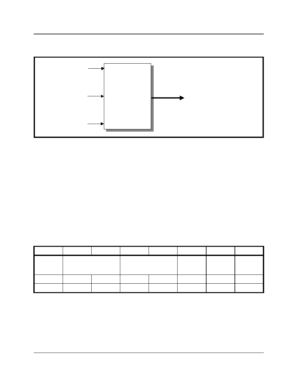
·Á
·Á
·Á
·Á
XRT7250
DS3/E3 FRAMER IC
REV. 1.1.1
271
In addition to taking data from multiple sources and
multiplexing them, in appropriate manner, to create
the outbound E3 frames, the Transmit E3 Framer
block has the following roles.
∑ Generating Alarm Conditions
∑ Generating Errored Frames (for testing purposes)
∑ Routing outbound E3 frames to the Transmit E3 LIU
Interface block
Each of these additional roles are discussed below.
5.2.4.2.1
Generating Alarm Conditions
The Transmit E3 Framer block permits the user to, by
writing the appropriate data into the on-chip registers,
to override the data that is being written into the
Transmit Payload Data and Overhead Data Input In-
terfaces and transmit the following alarm conditions.
∑ Generate the Yellow Alarms (or FERF indicators)
∑ Manipulate the A-bit, by forcing it to "0".
∑ Generate the AIS Pattern
∑ Generate the LOS pattern
∑ Generate FERF (Yellow) Alarms, in response to
detection of a Red Alarm condition (via the Receive
Section of the XRT7250).
The procedure and results of generating any of these
alarm conditions is presented below.
The user can exercise each of these options by writ-
ing the appropriate data to the Tx E3 Configuration
Register (Address = 0x30). The bit format of this reg-
ister is presented below.
Bit-fields 1 and 2 permit the user to transmit various
alarm conditions to the remote terminal equipment.
The role/function of each of these two bit-fields within
the register, are discussed below.
5.2.4.2.1.1
Tx AIS Enable - Bit 2
This read/write bit field permits the user to force the
transmission of an AIS (Alarm Indication Signal) pat-
tern to the remote terminal equipment via software
control. If the user opts to transmit an AIS pattern,
then the Transmit Section of the Framer IC will begin
to transmit an unframed all ones pattern to the re-
mote terminal equipment. Table 54 presents the rela-
tionship between the contents of this bit-field, and the
resulting Framer action.
F
IGURE
119. A S
IMPLE
I
LLUSTRATION
OF
THE
T
RANSMIT
E3 F
RAMER
B
LOCK
AND
THE
ASSOCIATED
PATHS
TO
OTHER
F
UNCTIONAL
B
LOCKS
Transmit
E3 Framer
Block
Transmit
E3 Framer
Block
Transmit HDLC
Controller/Buffer
Transmit Overhead
Data Input Interface
Transmit Payload Data
Input Interface
To Transmit E3 LIU Interface Block
TXE3 CONFIGURATION REGISTER (ADDRESS = 0X30)
B
IT
7
B
IT
6
B
IT
5
B
IT
4
B
IT
3
B
IT
2
B
IT
1
B
IT
0
Tx
BIP-4
Enable
TxASourceSel[1:0]
TxNSourceSel[1:0]
Tx AIS
Enable
Tx LOS
Enable
Tx FAS
Source
Select
R/W
R/W
R/W
R/W
R/W
R/W
R/W
R/W
0
0
0
0
0
0
0
0

XRT7250
·Á
·Á
·Á
·Á
DS3/E3 FRAMER IC
REV. 1.1.1
272
N
OTE
: This bit is ignored whenever the TxLOS bit-field is
set.
5.2.4.2.1.2
Transmit LOS Enable - Bit 1
This read/write bit field allows the user to transmit an
LOS (Loss of Signal) pattern to the remote terminal,
upon software control. Table 55 relates the contents
of this bit field to the Transmit E3 Framer block's ac-
tion.
N
OTE
: When this bit is set, it overrides all of the other bits in
this register.
5.2.4.2.1.3
Transmitting FERF (Far-End
Receive Failure) Indicator or Yellow Alarm
The XRT7250 Framer IC permits the user to control
the state of the "A" bit-field, within each outbound E3
frame. This can be achieved by writing the appropri-
ate data into the TxASource[1:0] bit-fields within the
Tx E3 Configuration Register, as illustrated below.
The following table presents the relationship between
the contents of TxASource[1:0] and the resulting
source of the "A" bit.
T
ABLE
54: T
HE
R
ELATIONSHIP
BETWEEN
THE
CONTENTS
OF
B
IT
2 (T
X
AIS E
NABLE
)
WITHIN
THE
T
X
E3
C
ONFIGURATION
R
EGISTER
,
AND
THE
RESULTING
T
RANSMIT
E3 F
RAMER
B
LOCK
'
S
A
CTION
B
IT
2
T
RANSMIT
E3 F
RAMER
'
S
A
CTION
0
Normal Operation:
The Transmit Section of the XRT7250 Framer IC will transmit E3 traffic based upon data that it accepts via the
Transmit Payload Data Input Interface block, the Transmit Overhead Data Input Interface block, the Transmit
HDLC Controller block and internally generated overhead bytes.
1
Transmit AIS Pattern:
The Transmit E3 Framer block will overwrite the E3 traffic, within an Unframed "All Ones" pattern.
T
ABLE
55: T
HE
R
ELATIONSHIP
BETWEEN
THE
CONTENTS
OF
B
IT
1 (T
X
LOS)
WITHIN
THE
T
X
E3 C
ONFIGURATION
R
EGISTER
,
AND
THE
RESULTING
T
RANSMIT
E3 F
RAMER
B
LOCK
'
S
A
CTION
B
IT
1
T
RANSMIT
E3 F
RAMER
'
S
A
CTION
0
Normal Operation:
The Overhead bits are either internally generated, or they are inserted via the Transmit Overhead Data Input
Interface or the Transmit HDLC Controller blocks. The Payload bits are received from the Transmit Payload
Data Input Interface.
1
Transmit LOS Pattern:
When this command is invoked the Transmit E3 Framer will do the following.
∑ Set all of the overhead bytes to "0" (including the FA1 and FA2 bytes)
Overwrite the E3 payload bits with an "all zeros" pattern.
TXE3 CONFIGURATION REGISTER (ADDRESS = 0X30)
B
IT
7
B
IT
6
B
IT
5
B
IT
4
B
IT
3
B
IT
2
B
IT
1
B
IT
0
Tx
BIP-4
Enable
TxASourceSel[1:0]
TxNSourceSel[1:0]
Tx AIS
Enable
Tx LOS
Enable
Tx FAS
Source
Select
R/W
R/W
R/W
R/W
R/W
R/W
R/W
R/W
0
X
X
0
0
0
0
0

·Á
·Á
·Á
·Á
XRT7250
DS3/E3 FRAMER IC
REV. 1.1.1
273
Hence, if a Yellow Alarm condition needs to be trans-
mitted to the Remote Terminal Equipment, this can
be accomplished by executing the following steps.
STEP 1 - Write a "1" into Bit 1 (A Bit) within the Tx
E3 Service Bits Register, as indicated below.
STEP 2 - Write the value "00" into the TxAS-
ource[1:0] bit-fields within the Tx E3 Configura-
tion Register, as indicated below.
These two steps will cause the Transmit E3 Framer
block to read in the contents of Bit 1 (within the Tx E3
Service Bit register) and insert it into the "A" bit-field
within the outbound E3 data stream. Hence, the "A"
bit will be set to "1", which will be interpreted as an
Alarm Condition, by the Remote Terminal Equipment.
5.2.4.2.2
Configuring the Transmit E3 Framer
block to insert the BIP-4 nibble into each out-
bound E3 frame.
The XRT7250 Framer IC permits the user to (1) con-
figure the Transmit Section of the device to insert the
BIP-4 value into each outbound E3 frame and (2) to
configure the Receive Section of the device to com-
pute and verify the BIP-4 value, within each inbound'
E3 frame.
These two configurations are accomplished by setting
bit 7 (Tx BIP-4 Enable), within the Tx E3 Configura-
tion Register, to "1", as indicated below.
T
X
AS
OURCE
S
EL
[1:0]
S
OURCE
OF
A B
IT
00
TxE3 Service Bits Register (Address = 0x35)
01
Transmit Overhead Data Input Interface
10
Transmit Payload Data Input Interface
11
Functions as a FEBE (Far-End-Block Error) bit-field.
This bit-field is set to "0", if the Near-End Receive Section (within this chip) detects no BIP-4
Errors within the incoming E3 frames.
This bit-field is set to "1", if the Near-End Receive Section (within this chip) detects a BIP-4
Error within the incoming E3 frame.
TXE3 SERVICE BITS REGISTER (ADDRESS = 0X35)
B
IT
7
B
IT
6
B
IT
5
B
IT
4
B
IT
3
B
IT
2
B
IT
1
B
IT
0
Not Used
A Bit
N Bit
RO
RO
RO
RO
RO
RO
R/W
R/W
0
0
0
0
0
0
1
0
TXE3 CONFIGURATION REGISTER (ADDRESS = 0X30)
B
IT
7
B
IT
6
B
IT
5
B
IT
4
B
IT
3
B
IT
2
B
IT
1
B
IT
0
Tx BIP-4
Enable
TxASourceSel[1:0]
TxNSourceSel[1:0]
Tx AIS
Enable
Tx LOS
Enable
Tx FAS
Source Select
R/W
R/W
R/W
R/W
R/W
R/W
R/W
R/W
X
0
0
X
X
X
X
X
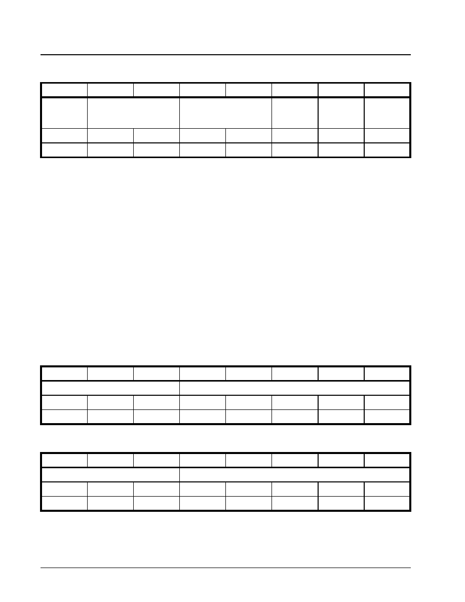
XRT7250
·Á
·Á
·Á
·Á
DS3/E3 FRAMER IC
REV. 1.1.1
274
Setting this bit-field to "1" accomplishes the following.
∑ It configures the Transmit E3 Framer block to com-
pute the BIP-4 value of a given E3 frame, and insert
in to the very last nibble, within the very next out-
bound E3 frame. (Hence, bits 1533 through 1536,
within each E3 frame, will function as the BIP-4
value)
∑ It configures the Receive E3 Framer block to com-
pute and verify the BIP-4 value of each incoming
E3 frame.
5.2.4.2.3
Generating Errored E3 Frames
The Transmit E3 Framer block permits the user to in-
sert errors into the framing and error detection over-
head bites (e.g., the FAS pattern, and the BIP-4 nib-
ble) of the outbound E3 data stream in order to sup-
port Remote Terminal Equipment testing. The user
can exercise this option by writing data into any of the
following registers.
∑ TxE3 FAS Error Mask Register - 0
∑ TxE3 FAS Error Mask Register - 1
∑ TxE3 BIP-4 Error Mask Register
Inserting Errors into the FAS pattern of the out-
bound' E3 frames.
The user can insert errors into the FAS pattern bits, of
each outbound E3 frame, by writing the appropriate
data into either the TxE3 FAS Error Mask Register - 0
or TxE3 FAS Error Mask Register - 1.
As the Transmit E3 Framer block formulates the out-
bound E3 frames, the contents of the FAS pattern bits
are automatically XORed with the contents of these
two registers. The results of this XOR operation is
written back into the corresponding bit-field within the
outbound E3 frame, and is transmitted to the Remote
Terminal Equipment. Therefore, if the user does not
wish to modify any of these bits, then these registers
must contain all "0's" (the default value).
Inserting Errors into the BIP-4 nibble, within each
outbound E3 frame.
The user can insert errors into the BIP-4 nibble, within
each outbound E3 frame, by writing the appropriate
data into the TxE3 BIP-4 Error Mask Register.
TXE3 CONFIGURATION REGISTER (ADDRESS = 0X30)
B
IT
7
B
IT
6
B
IT
5
B
IT
4
B
IT
3
B
IT
2
B
IT
1
B
IT
0
Tx
BIP-4
Enable
TxASourceSel[1:0]
TxNSourceSel[1:0]
Tx AIS
Enable
Tx LOS
Enable
Tx FAS
Source
Select
R/W
R/W
R/W
R/W
R/W
R/W
R/W
R/W
1
X
X
X
X
X
X
X
TXE3 FAS ERROR MASK REGISTER - 0 (ADDRESS = 0X48)
B
IT
7
B
IT
6
B
IT
5
B
IT
4
B
IT
3
B
IT
2
B
IT
1
B
IT
0
Not Used
TxFAS_Error_Mask_Upper[4:0]
RO
RO
RO
R/W
R/W
R/W
R/W
R/W
0
0
0
X
X
X
X
X
TXE3 FAS ERROR MASK REGISTER - 1 (ADDRESS = 0X49)
B
IT
7
B
IT
6
B
IT
5
B
IT
4
B
IT
3
B
IT
2
B
IT
1
B
IT
0
Not Used
TxFAS_Error_Mask_Lower[4:0]
RO
RO
RO
R/W
R/W
R/W
R/W
R/W
0
0
0
X
X
X
X
X

·Á
·Á
·Á
·Á
XRT7250
DS3/E3 FRAMER IC
REV. 1.1.1
275
As the Transmit E3 Framer block formulates the out-
bound E3 frames, the contents of the BIP-4 bits are
automatically XORed with the contents of this regis-
ter. The results of this XOR operation is written back
into the corresponding bit-field within the outbound
E3 frame, and is transmitted to the Remote Terminal
Equipment. Therefore, if the user does not wish to
modify any of these bits, then this register must con-
tain all "0's" (the default value).
N
OTE
: This register is only active if the XRT7250 Framer IC
has been configured to insert the BIP-4 nibble into each
outbound E3 frame.
5.2.5
The Transmit E3 Line Interface Block
The XRT7250 Framer IC is a digital device that takes
E3 payload and overhead bit information from some
terminal equipment, processes this data and ulti-
mately, multiplexes this information into a series of
outbound E3 frames. However, the XRT7250 Framer
IC lacks the current drive capability to be able to di-
rectly transmit this E3 data stream through some
transformer-coupled coax cable with enough signal
strength for it to be received by the remote receiver.
Therefore, in order to get around this problem, the
Framer IC requires the use of an LIU (Line Interface
Unit) IC. An LIU is a device that has sufficient drive
capability, along with the necessary pulse-shaping
circuitry to be able to transmit a signal through the
transmission medium in a manner that it can be reli-
ably received by the far-end receiver. Figure 120 pre-
sents a circuit drawing depicting the Framer IC inter-
facing to an LIU (XRT7300 DS3/E3/STS-1 Transmit
LIU).
TXE3 BIP-4 ERROR MASK REGISTER (ADDRESS = 0X4A)
B
IT
7
B
IT
6
B
IT
5
B
IT
4
B
IT
3
B
IT
2
B
IT
1
B
IT
0
Not Used
TxBIP-4 Mask[3:0]
R/W
R/W
R/W
R/W
R/W
R/W
R/W
R/W
0
0
0
0
0
0
0
0

XRT7250
·Á
·Á
·Á
·Á
DS3/E3 FRAMER IC
REV. 1.1.1
276
The Transmit Section of the XRT7250 contains a
block which is known as the Transmit E3 LIU Interface
block. The purpose of the Transmit E3 LIU Interface
block is to take the outbound E3 data stream, from
the Transmit E3 Framer block, and to do the following:
1. Encode this data into one of the following line
codes
a. Unipolar (e.g., Single-Rail)
b. AMI (Alternate Mark Inversion)
c. HDB3 (High Density Bipolar - 3)
2. And to transmit this data to the LIU IC.
Figure 121 presents a simple illustration of the Trans-
mit E3 LIU Interface block.
F
IGURE
120. A
PPROACH
TO
I
NTERFACING
THE
XRT7250 F
RAMER
IC
DEVICE
TO
THE
XRT7300 DS3/E3/STS-1 LIU
5V
U 1
X R T7250
TxP OS
65
TxN E G
64
TxLineC lk
63
D MO
79
E xtLOS
78
R LOL
77
LLOOP
69
R LOOP
70
TA OS
68
TxLE V
67
E N C OD IS
66
R E QB
71
R xP OS
76
R xN E G
75
R xLineC l k
74
MOTO
27
R E S E TB
28
A 0
15
A 1
16
A 2
17
A 3
18
A 4
19
A 5
20
A 6
21
A 7
22
A 8
23
D 0
32
D 1
33
D 2
34
D 3
35
D 4
36
D 5
37
D 6
38
D 7
39
R dy_D tck
6
W R B _R W
7
R D B _D S
10
C S B
8
A LE _A S
9
IN TB
13
TxS E R
46
TxInC lk
43
TxFrame
61
R xS er
86
R xC lk
88
R xFrame
90
R xLOS
95
R xOOF
94
R xR E D
93
R xA IS
87
N IB B LE IN TF
25
U 2
X R T7300
TP D A TA
37
TN D A TA
38
TC LK
36
R C LK 1
31
R N E G
32
R P OS
33
TTIP
41
TR IN G
40
MTIP
44
MR IN G
43
R R IN G
9
R TIP
8
D MO
4
R LOS
24
R LOL
23
LLB
14
R LB
15
TA OS
2
TxLE V
1
E N C OD IS
21
R E QD IS
12
T1
1:1
1
5
4
8
T2
1:1
1
5
4
8
R 1
36
1
2
R 2
36
1
2
R 6
37.5
1
2
R 3
270
1
2
R 4
270
1
2
R 5
37.5
1
2
C 1
0.01uF
1
2
TxS E R
TxInC lk
N IB B LE IN TF
R E S E TB
R TIP
R R IN G
C S B
R W
D S
A S
TxFrame
R xS er
R xC lk
R xFrame
R xLOS
R xOOF
R xR E D
R xA IS
A [8:0]
TR IN G
TTIP
IN TB
D [7:0]
IN TB
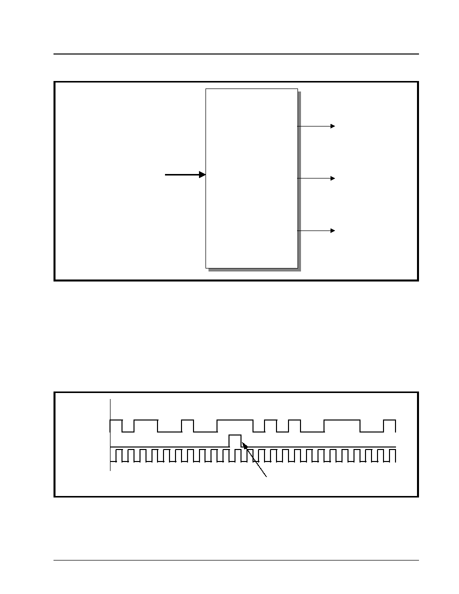
·Á
·Á
·Á
·Á
XRT7250
DS3/E3 FRAMER IC
REV. 1.1.1
277
The Transmit E3 LIU Interface block can transmit data
to the LIU IC or other external circuitry via two differ-
ent output modes: Unipolar or Bipolar. If the user se-
lects Unipolar (or Single Rail) mode, then the con-
tents of the E3 Frame is output, in a binary (NRZ
manner) data stream via the TxPOS pin to the LIU IC.
The TxNEG pin will only be used to denote the frame
boundaries. TxNEG will pulse "High" for one bit peri-
od, at the start of each new E3 frame, and will remain
"Low" for the remainder of the frame. Figure 122 pre-
sents an illustration of the TxPOS and TxNEG signals
during data transmission while the Transmit E3 LIU
Interface block is operating in the Unipolar mode.
This mode is sometimes referred to as Single Rail
mode because the data pulses only exist in one po-
larity: positive.
When the Transmit E3 LIU Interface block is operating
in the Bipolar (or Dual Rail) mode, then the contents
of the E3 Frame is output via both the TxPOS and Tx-
NEG pins. If the Bipolar mode is chosen, then E3 da-
ta can be transmitted to the LIU via one of two differ-
ent line codes: Alternate Mark Inversion (AMI) or High
Density Bipolar -3 (HDB3). Each one of these line
codes will be discussed below. Bipolar mode is
sometimes referred to as Dual Rail because the data
pulses occur in two polarities: positive and negative.
F
IGURE
121. A S
IMPLE
I
LLUSTRATION
OF
THE
T
RANSMIT
E3 LIU I
NTERFACE
BLOCK
From Transmit E3
Framer Block
TxPOS
TxNEG
TxLineClk
Transmit E3
LIU Interface
Block
F
IGURE
122. T
HE
B
EHAVIOR
OF
T
X
POS
AND
T
X
NEG
SIGNALS
DURING
DATA
TRANSMISSION
WHILE
THE
T
RANSMIT
DS3 LIU I
NTERFACE
IS
OPERATING
IN
THE
U
NIPOLAR
M
ODE
TxPOS
TxNEG
TxLineClk
Data
1 0 1 1 0 0 1 0 0 1 1 1 0 1 0 1 0 0 1 1 1 0 0 1
Frame Boundary
XRT7250
·Á
·Á
·Á
·Á
DS3/E3 FRAMER IC
REV. 1.1.1
278
The role of the TxPOS, TxNEG and TxLineClk output
pins, for this mode are discussed below.
TxPOS - Transmit Positive Polarity Pulse: The
Transmit E3 LIU Interface block will assert this output
to the LIU IC when it desires for the LIU to generate
and transmit a positive polarity pulse to the remote
terminal equipment.
TxNEG - Transmit Negative Polarity Pulse: The
Transmit E3 LIU Interface block will assert this output
to the LIU IC when it desires for the LIU to generate
and transmit a negative polarity pulse to the remote
terminal equipment.
TxLineClk - Transmit Line Clock: The LIU IC uses
this signal from the Transmit E3 LIU Interface block to
sample the state of its TxPOS and TxNEG inputs.
The results of this sampling dictates the type of pulse
(positive polarity, zero, or negative polarity) that it will
generate and transmit to the remote Receive E3
Framer.
5.2.5.1
Selecting the various Line Codes
The user can select either the Unipolar Mode or Bipo-
lar Mode by writing the appropriate value to Bit 3 of
the I/O Control Register (Address = 0x01), as shown
below.
Table 56 relates the value of this bit field to the Trans-
mit E3 LIU Interface Output Mode.
N
OTES
:
1. The default condition is the Bipolar Mode.
2. This selection also effects the operation of the
Receive E3 LIU Interface block
5.2.5.1.1
The Bipolar Mode Line Codes
If the Framer is choosen to operate in the Bipolar
Mode, then the DS3 data-stream can be choosen to
be transmitted via the AMI (Alternate Mark Inversion)
or the HDB3 Line Codes. The definition of AMI and
HDB3 line codes follow.
5.2.5.1.1.1
The AMI Line Code
AMI or Alternate Mark Inversion, means that consec-
utive "one's" pulses (or marks) will be of opposite po-
larity with respect to each other. The line code in-
volves the use of three different amplitude levels: +1,
0, and -1. +1 and -1 amplitude signals are used to
represent one's (or mark) pulses and the "0" ampli-
tude pulses (or the absence of a pulse) are used to
represent zeros (or space) pulses. The general rule
for AMI is: if a given mark pulse is of positive polarity,
then the very next mark pulse will be of negative po-
larity and vice versa. This alternating-polarity rela-
tionship exists between two consecutive mark pulses,
independent of the number of 'zeros' that may exist
between these two pulses. Figure 123 presents an il-
lustration of the AMI Line Code as would appear at
the TxPOS and TxNEG pins of the Framer, as well as
the output signal on the line.
I/O CONTROL REGISTER (ADDRESS = 0X01)
B
IT
7
B
IT
6
B
IT
5
B
IT
4
B
IT
3
B
IT
2
B
IT
1
B
IT
0
Disable TxLOC
LOC
Disable
RxLOC
AMI/ZeroSup*
Unipolar/
Bipolar*
TxLine CLK
Invert
RxLine CLK
Invert
Reframe
R/W
RO
R/W
R/W
R/W
R/W
R/W
R/W
1
0
1
0
0
0
0
0
T
ABLE
56: T
HE
R
ELATIONSHIP
BETWEEN
THE
CONTENT
OF
B
IT
3 (U
NIPOLAR
/B
IPOLAR
*)
WITHIN
THE
UNI I/O
C
ONTROL
R
EGISTER
AND
THE
T
RANSMIT
E3 F
RAMER
L
INE
I
NTERFACE
O
UTPUT
M
ODE
B
IT
3
T
RANSMIT
E3 F
RAMER
LIU I
NTERFACE
O
UTPUT
M
ODE
0
Bipolar Mode: AMI or HDB3 Line Codes are Transmitted and Received
1
Unipolar (Single Rail) Mode of transmission and reception of E3 data is selected.
·Á
·Á
·Á
·Á
XRT7250
DS3/E3 FRAMER IC
REV. 1.1.1
279
N
OTE
: One of the main reasons that the AMI Line Code
has been chosen for driving transformer-coupled media is
that this line code introduces no dc component, thereby
minimizing dc distortion in the line.
5.2.5.1.1.2
The HDB3 Line Code
The Transmit E3 Framer and the associated LIU IC
combine the data and timing information (originating
from the TxLineClk signal) into the line signal that is
transmitted to the remote receiver. The remote re-
ceiver has the task of recovering this data and timing
information from the incoming E3 data stream. Many
clock and data recovery schemes rely on the use of
Phase Locked Loop technology. Phase-Locked-Loop
(PLL) technology for clock recovery relies on transi-
tions in the line signal, in order to maintain lock with
the incoming E3 data stream. However, PLL-based
clock recovery scheme, are vulnerable to the occur-
rence of a long stream of consecutive zeros (e.g., the
absence of transitions). This scenario can cause the
PLL to lose lock with the incoming E3 data, thereby
causing the clock and data recovery process of the
receiver to fail. Therefore, some approach is needed
to insure that such a long string of consecutive zeros
can never happen. One such technique is HDB3 en-
coding. HDB3 (or High Density Bipolar - 3) is a form
of AMI line coding that implements the following rule.
In general the HDB3 line code behaves just like AMI
with the exception of the case when a long string of
consecutive zeros occur on the line. Any string of 4
consecutive zeros will be replaced with either a
"000V" or a "B00V" where "B" refers to a Bipolar
pulse (e.g., a pulse with a polarity that is compliant
with the AMI coding rule). And "V" refers to a Bipolar
Violation pulse (e.g., a pulse with a polarity that vio-
lates the alternating polarity scheme of AMI.) The de-
cision between inserting an "000V" or a "B00V" is
made to insure that an odd number of Bipolar (B)
pulses exist between any two Bipolar Violation (V)
pulses. Figure 124 presents a timing diagram that il-
lustrates examples of HDB3 encoding.
The user chooses between AMI or HDB3 line coding
by writing to bit 4 of the I/O Control Register (Address
= 0x01), as shown below.
F
IGURE
123. I
LLUSTRATION
OF
AMI L
INE
C
ODE
Data
TxPOS
TxNEG
Line Signal
1 0 1 1 0 0 0 1 0 1 1 1 1 0 1 1 0 1 1 0 0 1 1 0 0 0 0 1
F
IGURE
124. I
LLUSTRATION
OF
TWO
EXAMPLES
OF
HDB3 E
NCODING
Data
T x P O S
T x N E G
TxLineClk
Line Signal
0
0
0
V
B
0
0
V
1
0
1
1
1
1
1
1
1
1
0
0
0
0
0
0
0
0
1
1
1
0
0
0
0
0
1
1
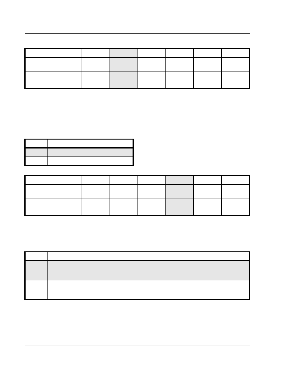
XRT7250
·Á
·Á
·Á
·Á
DS3/E3 FRAMER IC
REV. 1.1.1
280
Table 57 relates the content of this bit-field to the Bi-
polar Line Code that E3 Data will be transmitted and
received at.
N
OTES
:
1. This bit is ignored if the Unipolar mode is selected.
2. This selection also effects the operation of the
Receive E3 LIU Interface block
5.2.5.2
TxLineClk Clock Edge Selection
The Framer also allows the user to specify whether
the E3 output data (via TxPOS and/or TxNEG output
pins) is to be updated on the rising or falling edges of
the TxLineClk signal. This selection is made by writ-
ing to bit 2 of the I/O Control Register, as depicted be-
low.
Table 58 relates the contents of this bit field to the
clock edge of TxClk that E3 Data is output on the Tx-
POS and/or TxNEG output pins.
N
OTE
: The user will typically make the selection based
upon the set-up and hold time requirements of the Transmit
LIU IC.
I/O CONTROL REGISTER (ADDRESS = 0X01)
B
IT
7
B
IT
6
B
IT
5
B
IT
4
B
IT
3
B
IT
2
B
IT
1
B
IT
0
Disable TxLOC
LOC
Disable
RxLOC
AMI/ZeroSup*
Unipolar/
Bipolar*
TxLine CLK
Invert
RxLine CLK
Invert
Reframe
R/W
RO
R/W
R/W
R/W
R/W
R/W
R/W
1
0
1
0
0
0
0
0
T
ABLE
57: T
HE
R
ELATIONSHIP
BETWEEN
B
IT
4 (AMI/
HDB3*)
WITHIN
THE
I/O C
ONTROL
R
EGISTER
AND
THE
B
IPOLAR
L
INE
C
ODE
THAT
IS
OUTPUT
BY
THE
T
RANSMIT
E3 LIU I
NTERFACE
B
LOCK
B
IT
4
B
IPOLAR
L
INE
C
ODE
0
HDB3
1
AMI
II/O CONTROL REGISTER (ADDRESS = 0X01)
B
IT
7
B
IT
6
B
IT
5
B
IT
4
B
IT
3
B
IT
2
B
IT
1
B
IT
0
Disable TxLOC
LOC
Disable
RxLOC
AMI/ZeroSup*
Unipolar/
Bipolar*
TxLine CLK
Invert
RxLine CLK
Invert
Reframe
R/W
RO
R/W
R/W
R/W
R/W
R/W
R/W
1
0
1
0
0
0
0
0
T
ABLE
58: T
HE
R
ELATIONSHIP
BETWEEN
THE
CONTENTS
OF
B
IT
2 (T
X
L
INE
C
LK
I
NV
)
WITHIN
THE
I/O C
ONTROL
R
EGISTER
AND
THE
T
X
L
INE
C
LK
CLOCK
EDGE
THAT
T
X
POS
AND
T
X
NEG
ARE
UPDATED
ON
B
IT
2
R
ESULT
0
Rising Edge:
Outputs on TxPOS and/or TxNEG are updated on the rising edge of TxLineClk.
See Figure 125 for timing relationship between TxLineClk, TxPOS and TxNEG signals, for this selection.
1
Falling Edge:
Outputs on TxPOS and/or TxNEG are updated on the falling edge of TxLineClk.
See Figure 126 for timing relationship between TxLineClk, TxPOS and TxNEG signals, for this selection.

·Á
·Á
·Á
·Á
XRT7250
DS3/E3 FRAMER IC
REV. 1.1.1
281
5.2.6
Transmit Section Interrupt Processing
The Transmit Section of the XRT7250 can generate
an interrupt to the Microprocessor/Microcontroller for
the following reasons.
∑ Completion of Transmission of LAPD Message
5.2.6.1
Enabling Transmit Section Interrupts
The Interrupt Structure, within the XRT7250 contains
two hierarchical levels:
∑ Block Level
∑ Source Level
The Block Level
The Enable State of the Block Level for the Transmit
Section Interrupts dictates whether or not interrupts
(enabled) at the source level, are actually enabled.
The user can enable or disable these Transmit Sec-
tion interrupts, at the Block Level by writing the appro-
priate data into Bit 1 (Tx DS3/E3 Interrupt Enable)
within the Block Interrupt Enable register (Address =
0x04), as illustrated below.
F
IGURE
125. W
AVEFORM
/T
IMING
R
ELATIONSHIP
BETWEEN
T
X
L
INE
C
LK
, T
X
POS
AND
T
X
NEG - T
X
POS
AND
T
X
NEG
ARE
CONFIGURED
TO
BE
UPDATED
ON
THE
RISING
EDGE
OF
T
X
L
INE
C
LK
TxLineClk
TxPOS
TxNEG
t32
t30
t33
F
IGURE
126. W
AVEFORM
/T
IMING
R
ELATIONSHIP
BETWEEN
T
X
L
INE
C
LK
, T
X
POS
AND
T
X
NEG - T
X
POS
AND
T
X
NEG
ARE
CONFIGURED
TO
BE
UPDATED
ON
THE
FALLING
EDGE
OF
T
X
L
INE
C
LK
TxLineClk
TxPOS
TxNEG
t31
t32
t33

XRT7250
·Á
·Á
·Á
·Á
DS3/E3 FRAMER IC
REV. 1.1.1
282
Setting this bit-field to "1" enables the Transmit Sec-
tion (at the Block Level) for Interrupt Generation.
Conversely, setting this bit-field to "0" disables the
Transmit Section for interrupt generation.
What does it mean for the Transmit Section Inter-
rupts to be enabled or disabled at the Block Lev-
el?
If the Transmit Section is disabled (for interrupt gener-
ation) at the Block Level, then ALL Transmit Section
interrupts are disabled, independent of the interrupt
enable/disable state of the source level interrupts.
If the Transmit Section is enabled (for interrupt gener-
ation) at the block level, then a given interrupt will be
enabled at the source level. Conversely, if the Trans-
mit Section is enabled (for interrupt generation) at the
Block level, then a given interrupt will still be disabled,
if it is disabled at the source level.
As mentioned earlier, the Transmit Section of the
XRT7250 Framer IC contains the Completion of
Transmission of LAPD Message Interrupt.
The Enabling/Disabling and Servicing of this interrupt
is presented below.
5.2.6.1.1
The Completion of Transmission of
the LAPD Message Interrupt
If the Transmit Section interrupts have been enabled
at the Block level, then the user can enable or disable
the Completion of Transmission of a LAPD Message
Interrupt, by writing the appropriate value into Bit 1
(TxLAPD Interrupt Enable) within the Tx E3 LAPD
Status & Interrupt Register (Address = 0x34), as illus-
trated below.
Setting this bit-field to "1' enables the Completion of
Transmission of a LAPD Message Interrupt. Con-
versely, setting this bit-field to "0" disables the Com-
pletion of Transmission of a LAPD Message interrupt.
5.2.6.1.2
Servicing the Completion of Trans-
mission of a LAPD Message Interrupt
As mentioned previously, once the user commands
the LAPD Transmitter to begin its transmission of a
LAPD Message, it will do the following.
1. It will parse through the contents of the Transmit
LAPD Message Buffer (located at address loca-
tions 0x86 through 0xDD) and search for a string
of five (5) consecutive "1's". If the LAPD Trans-
mitter finds a string of five consecutive "1's"
(within the content of the LAPD Message Buffer,
then it will insert a "0" immediately after this
string.
2. It will compute the FCS (Frame Check Sequence)
value and append this value to the back-end of
the user-message.
3. It will read out of the content of the user (zero-
stuffed) message and will encapsulate this data
into a LAPD Message frame.
4. Finally, it will begin transmitting the contents of
this LAPD Message frame via the "N" bits, within
each outbound E3 frame.
5. Once the LAPD Transmitter has completed its
transmission of this LAPD Message frame (to the
BLOCK INTERRUPT ENABLE REGISTER (ADDRESS = 0X04)
B
IT
7
B
IT
6
B
IT
5
B
IT
4
B
IT
3
B
IT
2
B
IT
1
B
IT
0
RxDS3/E3
Interrupt
Enable
Not Used
TxDS3/E3
Interrupt
Enable
One-Second
Interrupt
Enable
R/W
RO
RO
RO
RO
RO
R/W
R/W
0
0
0
0
0
0
0
0
TXE3 LAPD STATUS AND INTERRUPT REGISTER (ADDRESS = 0X34)
B
IT
7
B
IT
6
B
IT
5
B
IT
4
B
IT
3
B
IT
2
B
IT
1
B
IT
0
Not Used
TXDL Start
TXDL Busy
TxLAPD
Interrupt
Enable
TxLAPD
Interrupt
Status
RO
RO
RO
RO
R/W
RO
R/W
RUR
0
0
0
0
0
0
X
0
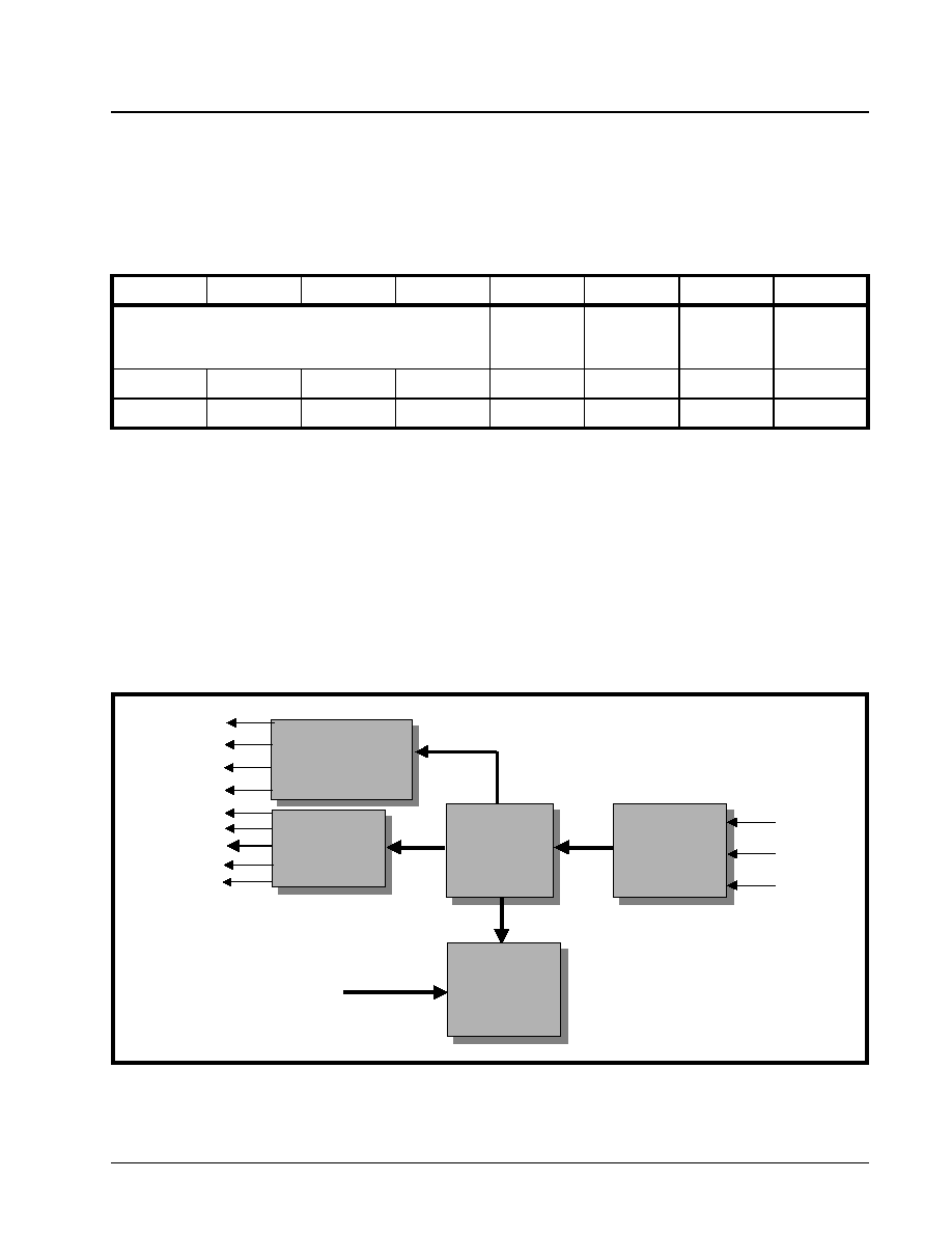
·Á
·Á
·Á
·Á
XRT7250
DS3/E3 FRAMER IC
REV. 1.1.1
283
Remote Terminal Equipment), the XRT7250
Framer IC will generate the Completion of Trans-
mission of a LAPD Message Interrupt to the
Microcontroller/Microprocessor. Once the
XRT7250 Framer IC generates this interrupt, it
will do the following.
∑ Assert the Interrupt Output pin (INT) by toggling it
"Low".
∑ Set Bit 0 (TxLAPD Interrupt Status) within the TxE3
LAPD Status and Interrupt Register, to "1" as illus-
trated below.
The purpose of this interrupt is to alert the Microcon-
troller/MIcroprocessor that the LAPD Transmitter has
completed its transmission of a given LAPD (or PM-
DL) Message, and is now ready to transmit the next
PMDL Message, to the Remote Terminal Equipment.
5.3
T
HE
R
ECEIVE
S
ECTION
OF
THE
XRT7250 (E3
M
ODE
O
PERATION
)
When the XRT7250 has been configured to operate
in the E3 Mode, the Receive Section of the XRT7250
consists of the following functional blocks.
∑ Receive LIU Interface block
∑ Receive HDLC Controller block
∑ Receive E3 Framer block
∑ Receive Overhead Data Output Interface block
∑ Receive Payload Data Output Interface block
Figure 127 presents a simple illustration of the Re-
ceive Section of the XRT7250 Framer IC.
Each of these functional blocks will be discussed in
detail in this document.
5.3.1
The Receive E3 LIU Interface Block
The purpose of the Receive E3 LIU Interface block is
two-fold:
TXE3 LAPD STATUS AND INTERRUPT REGISTER (ADDRESS = 0X34)
B
IT
7
B
IT
6
B
IT
5
B
IT
4
B
IT
3
B
IT
2
B
IT
1
B
IT
0
Not Used
TXDL Start
TXDL Busy
TxLAPD
Interrupt
Enable
TxLAPD
Interrupt
Status
RO
RO
RO
RO
R/W
RO
R/W
RUR
0
0
0
0
0
0
0
1
F
IGURE
127. A S
IMPLE
I
LLUSTRATION
OF
THE
R
ECEIVE
S
ECTION
OF
THE
XRT7250
CONFIGURED
TO
OPERATE
IN
THE
E3 M
ODE
Receive
Payload Data
Input
Interface Block
Receive DS3/E3
Framer Block
Receive LIU
Interface
Block
RxSer
RxNib[3:0]
RxClk
RxPOS
RxNEG
RxLineClk
Receive Overhead
Input
Interface Block
RxOHClk
RxOHInd
RxOH
RxOHEnable
RxOHFrame
RxFrame
Rx E3 HDLC
Controller/Buffer
Rx E3 HDLC
Controller/Buffer
From Microprocessor
Interface Block

XRT7250
·Á
·Á
·Á
·Á
DS3/E3 FRAMER IC
REV. 1.1.1
284
1. To receive encoded digital data from the E3 LIU
IC.
2. To decode this data, convert it into a binary data
stream and to route this data to the Receive E3
Framer block.
Figure 128 presents a simple illustration of the Re-
ceive E3 LIU Interface block.
The Receive Section of the XRT7250 will via the Re-
ceive E3 LIU Interface Block receive timing and data
information from the incoming E3 data stream. The
E3 Timing information will be received via the RxLi-
neClk input pin and the E3 data information will be re-
ceived via the RxPOS and RxNEG input pins. The
Receive E3 LIU Interface block is capable of receiving
E3 data pulses in unipolar or bipolar format. If the
Receive E3 framer is operating in the bipolar format,
then it can be configured to decode either AMI or
HDB3 line code data. Each of these input formats
and line codes will be discussed in detail, below.
5.3.1.1
Unipolar Decoding
If the Receive E3 LIU Interface block is operating in
the Unipolar (single-rail) mode, then it will receive the
Single Rail NRZ DS3 data pulses via the RxPOS in-
put pin. The Receive E3 LIU Interface block will also
receive its timing signal via the RxLineClk signal.
N
OTE
: The RxLineClk signal will function as the timing
source for the entire Receive Section of the XRT7250.
No data pulses will be applied to the RxNEG input
pin. The Receive E3 LIU Interface block receives a
logic "1" when a logic "1" level signal is present at the
RxPOS pin, during the sampling edge of the RxLi-
neClk signal. Likewise, a logic "0" is received when a
logic "0" level signal is applied to the RxPOS pin.
Figure 129 presents an illustration of the behavior of
the RxPOS, RxNEG and RxLineClk input pins when
the Receive E3 LIU Interface block is operating in the
Unipolar mode.
F
IGURE
128. A S
IMPLE
I
LLUSTRATION
OF
THE
R
ECEIVE
E3 LIU I
NTERFACE
B
LOCK
RxPOS
RxNEG
RxLineClk
To Receive E3
Framer Block
Receive E3
LIU Interface
Block
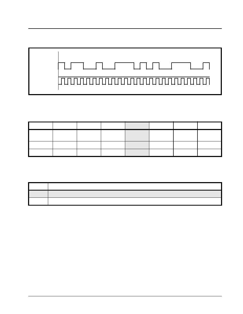
·Á
·Á
·Á
·Á
XRT7250
DS3/E3 FRAMER IC
REV. 1.1.1
285
The user can configure the Receive E3 LIU Interface
block to operate in either the Unipolar or the Bipolar
Mode by writing the appropriate data to the I/O Con-
trol Register, as depicted below.
Table 59 relates the value of this bit-field to the Re-
ceive E3 LIU Interface Input Mode.
N
OTES
:
1. The default condition is the Bipolar Mode.
2. This selection also effects the Transmit E3 Framer
Line Interface Output Mode
5.3.1.2
Bipolar Decoding
If the Receive E3 LIU Interface block is operating in
the Bipolar Mode, then it will receive the E3 data puls-
es via both the RxPOS, RxNEG, and the RxLineClk
input pins. Figure 130 presents a circuit diagram il-
lustrating how the Receive E3 LIU Interface block in-
terfaces to the Line Interface Unit while the Framer is
operating in Bipolar mode. The Receive E3 LIU Inter-
face block can be configured to decode either the AMI
or HDB3 line codes.
F
IGURE
129. B
EHAVIOR
OF
THE
R
X
POS, R
X
NEG
AND
R
X
L
INE
C
LK
SIGNALS
DURING
DATA
RECEPTION
OF
U
NIPO
-
LAR
D
ATA
RxPOS
RxNEG
RxLineClk
Data
1 0 1 1 0 0 1 0 0 1 1 1 0 1 0 1 0 0 1 1 1 0 0 1
II/O CONTROL REGISTER (ADDRESS = 0X01)
B
IT
7
B
IT
6
B
IT
5
B
IT
4
B
IT
3
B
IT
2
B
IT
1
B
IT
0
Disable TxLOC
LOC
Disable
RxLOC
AMI/ZeroSup*
Unipolar/
Bipolar*
TxLine CLK
Invert
RxLine CLK
Invert
Reframe
R/W
RO
R/W
R/W
R/W
R/W
R/W
R/W
1
0
1
0
0
0
0
0
T
ABLE
59: T
HE
R
ELATIONSHIP
BETWEEN
THE
CONTENTS
OF
B
IT
2 (T
X
L
INE
C
LK
I
NV
)
WITHIN
THE
I/O C
ONTROL
R
EGISTER
AND
THE
T
X
L
INE
C
LK
CLOCK
EDGE
THAT
T
X
POS
AND
T
X
NEG
ARE
UPDATED
ON
B
IT
3
R
ECEIVE
E3 LIU I
NTERFACE
I
NPUT
M
ODE
0
.Bipolar Mode (Dual Rail): AMI or HDB3 Line Codes are Transmitted and Received.
1
Unipolar Mode (Single Rail) Mode of transmission and reception of E3 data is selected.
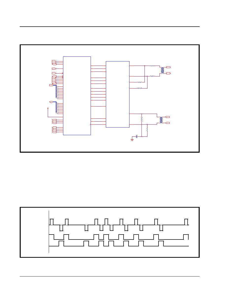
XRT7250
·Á
·Á
·Á
·Á
DS3/E3 FRAMER IC
REV. 1.1.1
286
5.3.1.2.1
AMI Decoding
AMI or Alternate Mark Inversion, means that consec-
utive "one's" pulses (or marks) will be of opposite po-
larity with respect to each other. This line code in-
volves the use of three different amplitude levels: +1,
0, and -1. The +1 and -1 amplitude signals are used
to represent one's (or mark) pulses and the "0" ampli-
tude pulses (or the absence of a pulse) are used to
represent zeros (or space) pulses. The general rule
for AMI is: if a given mark pulse is of positive polarity,
then the very next mark pulse will be of negative po-
larity and vice versa. This alternating-polarity rela-
tionship exists between two consecutive mark pulses,
independent of the number of zeros that exist be-
tween these two pulses. Figure 131 presents an illus-
tration of the AMI Line Code as would appear at the
RxPOS and RxNEG pins of the Framer, as well as the
output signal on the line.
N
OTE
: One of the reasons that the AMI Line Code has
been chosen for driving copper medium, isolated via trans-
formers, is that this line code has no dc component, thereby
eliminating dc distortion in the line.
F
IGURE
130. I
LLUSTRATION
ON
HOW
THE
R
ECEIVE
E3 F
RAMER
(
WITHIN
THE
XRT7250 F
RAMER
IC)
BEING
INTER
-
FACE
TO
THE
XRT7300 L
INE
I
NTERFACE
U
NIT
,
WHILE
THE
F
RAMER
IS
OPERATING
IN
B
IPOLAR
M
ODE
5V
U1
XRT7250
TxPOS
65
TxNEG
64
TxLineClk
63
D M O
79
ExtLOS
78
RLOL
77
LLOOP
69
RLOOP
70
TAOS
68
TxLEV
67
ENCODIS
66
REQB
71
RxPOS
76
RxNEG
75
RxLineClk
74
MOTO
27
RESETB
28
A0
15
A1
16
A2
17
A3
18
A4
19
A5
20
A6
21
A7
22
A8
23
D0
32
D1
33
D2
34
D3
35
D4
36
D5
37
D6
38
D7
39
Rdy_Dtck
6
W R B _ R W
7
RDB_DS
10
CSB
8
ALE_AS
9
INTB
13
TxSER
46
TxInClk
43
TxFrame
61
RxSer
86
RxClk
88
RxFrame
90
RxLOS
95
RxOOF
94
RxRED
93
RxAIS
87
NIBBLEINTF
25
U2
XRT7300
TPDATA
37
TNDATA
38
TCLK
36
RCLK1
31
RNEG
32
RPOS
33
TTIP
41
TRING
40
MTIP
44
MRING
43
RRING
9
RTIP
8
D M O
4
RLOS
24
RLOL
23
LLB
14
RLB
15
TAOS
2
TxLEV
1
ENCODIS
21
REQDIS
12
T1
1:1
1
5
4
8
T2
1:1
1
5
4
8
R1
36
1
2
R2
36
1
2
R6
37.5
1
2
R3
270
1
2
R4
270
1
2
R5
37.5
1
2
C1
0.01uF
1
2
TxSER
TxInClk
NIBBLEINTF
RESETB
RTIP
RRING
CSB
R W
DS
AS
TxFrame
RxSer
RxClk
RxFrame
RxLOS
RxOOF
RxRED
RxAIS
A[8:0]
TRING
TTIP
INTB
D[7:0]
INTB
F
IGURE
131. I
LLUSTRATION
OF
AMI L
INE
C
ODE
Data 1 0 1 1 0 0 0 1 0 1 1 1 1 0 1 1 0 1 1 0 0 1 1 0 0 0 0 1
RxPOS
RxNEG
Line Signal
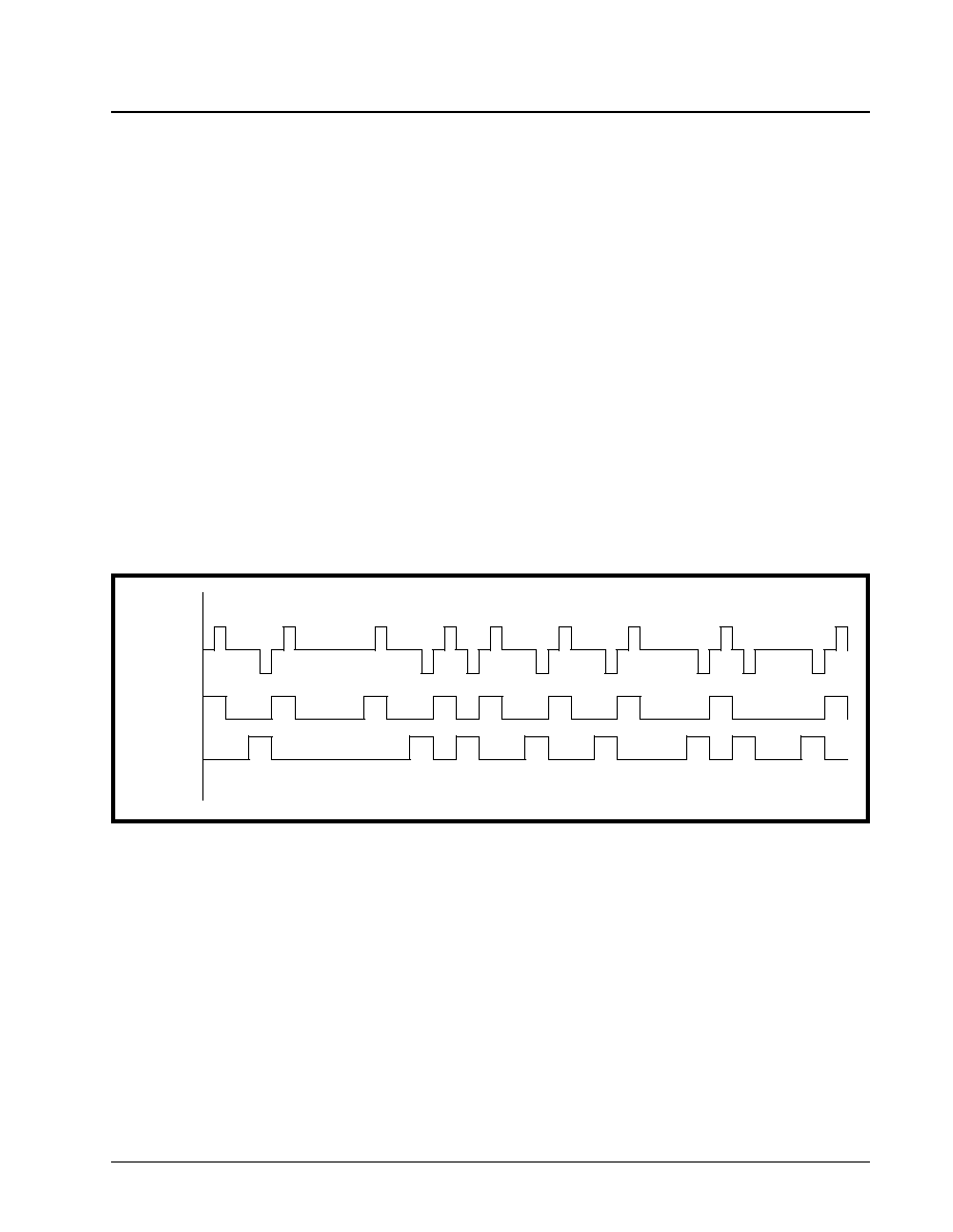
·Á
·Á
·Á
·Á
XRT7250
DS3/E3 FRAMER IC
REV. 1.1.1
287
5.3.1.2.2
HDB3 Decoding
The Transmit E3 LIU Interface block and the associat-
ed LIU embed and combine the data and clocking in-
formation into the line signal that is transmitted to the
remote terminal equipment. The remote terminal
equipment has the task of recovering this data and
timing information from the incoming E3 data stream.
Most clock and data recovery schemes rely on the
use of Phase-Locked-Loop technology. One of the
problems of using Phase-Locked-Loop (PLL) technol-
ogy for clock recovery is that it relies on transitions in
the line signal, in order to maintain lock with the in-
coming E3 data-stream. Therefore, these clock re-
covery scheme, are vulnerable to the occurrence of a
long stream of consecutive zeros (e.g., no transitions
in the line). This scenario can cause the PLL to lose
lock with the incoming E3 data, thereby causing the
clock and data recovery process of the receiver to fail.
Therefore, some approach is needed to insure that
such a long string of consecutive zeros can never
happen. One such technique is HDB3 (or High Den-
sity Bipolar -3) encoding.
In general the HDB3 line code behaves just like AMI
with the exception of the case when a long string of
consecutive zeros occurs on the line. Any 4 consecu-
tive zeros will be replaced with either a "000V" or a
"B00V" where "B" refers to a Bipolar pulse (e.g., a
pulse with a polarity that is compliant with the AMI
coding rule). And "V" refers to a Bipolar Violation
pulse (e.g., a pulse with a polarity that violates the al-
ternating polarity scheme of AMI.) The decision be-
tween inserting an "000V" or a "B00V" is made to in-
sure that an odd number of Bipolar (B) pulses exist
between any two Bipolar Violation (V) pulses. The
Receive E3 LIU Interface block, when operating with
the HDB3 Line Code is responsible for decoding the
HD-encoded data back into a unipolar (binary-for-
mat). For instance, if the Receive E3 LIU Interface
block detects a "000V" or a "B00V" pattern in the in-
coming pattern, the Receive E3 LIU Interface block
will replace it with four (4) consecutive zeros.
Figure 132 presents a timing diagram that illustrates
examples of HDB3 decoding.
5.3.1.2.3
Line Code Violations
The Receive E3 LIU Interface block will also check
the incoming E3 data stream for line code violations.
For example, when the Receive E3 LIU Interface
block detects a valid bipolar violation (e.g., in HDB3
line code), it will substitute four zeros into the binary
data stream. However, if the bipolar violation is in-
valid, then an LCV (Line Code Violation) is flagged
and the PMON LCV Event Count Register (Address =
0x50 and 0x51) will also be incremented. Additional-
ly, the LCV-One-Second Accumulation Registers (Ad-
dress = 0x6E and 0x6F) will be incremented. For ex-
ample: If the incoming E3 data is HDB3 encoded, the
Receive E3 LIU Interface block will also increment the
LCV One-Second Accumulation Register if three (or
more) consecutive zeros are received.
5.3.1.2.4
RxLineClk Clock Edge Selection
The incoming unipolar or bipolar data, applied to the
RxPOS and the RxNEG input pins are clocked into
the Receive E3 LIU Interface block via the RxLineClk
signal. The Framer IC allows the user to specify
which edge (e.g, rising or falling) of the RxLineClk
signal will sample and latch the signal at the RxPOS
and RxNEG input signals into the Framer IC. The us-
er can make this selection by writing the appropriate
data to bit 1 of the I/O Control Register, as depicted
below.
F
IGURE
132. I
LLUSTRATION
OF
TWO
EXAMPLES
OF
HDB3 D
ECODING
Line Signal
0
0
0
V
B
0
0
V
RxNEG
RxPOS
Data
1
0
1
1
1
1
1
1
1
1
0
0
0
0
0
0
0
0
1
1
1
0
0
0
0
0
1
1
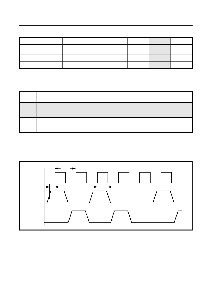
XRT7250
·Á
·Á
·Á
·Á
DS3/E3 FRAMER IC
REV. 1.1.1
288
Table 60 depicts the relationship between the value of
this bit-field to the sampling clock edge of RxLineClk.
Figure 133 and Figure 134 present the Waveform and
Timing Relationships between RxLineClk, RxPOS
and RxNEG for each of these configurations.
II/O CONTROL REGISTER (ADDRESS = 0X01)
B
IT
7
B
IT
6
B
IT
5
B
IT
4
B
IT
3
B
IT
2
B
IT
1
B
IT
0
Disable
TxLOC
LOC
Disable
RxLOC
AMI/ZeroSup*
Unipolar/
Bipolar*
TxLine CLK
Invert
RxLine CLK
Invert
Reframe
R/W
RO
R/W
R/W
R/W
R/W
R/W
R/W
1
0
1
0
0
0
0
0
T
ABLE
60: T
HE
R
ELATIONSHIP
BETWEEN
THE
CONTENTS
OF
B
IT
1 (R
X
L
INE
C
LK
I
NV
)
OF
THE
I/O C
ONTROL
R
EGISTER
,
AND
THE
SAMPLING
EDGE
OF
THE
R
X
L
INE
C
LK
SIGNAL
R
X
CLKI
NV
(B
IT
1)
R
ESULT
0
.Rising Edge:
RxPOS and RxNEG are sampled at the rising edge of RxLineClk. See Figure 133 for timing relationship
between RxLineClk, RxPOS, and RxNEG.
1
Falling Edge:
RxPOS and RxNEG are sampled at the falling edge of RxLineClk. See Figure 134 for timing relationship
between RxLineClk, RxPOS, and RxNEG.
F
IGURE
133. W
AVEFORM
/T
IMING
R
ELATIONSHIP
BETWEEN
R
X
L
INE
C
LK
, R
X
POS
AND
R
X
NEG - W
HEN
R
X
POS
AND
R
X
NEG
ARE
TO
BE
SAMPLED
ON
THE
RISING
EDGE
OF
R
X
L
INE
C
LK
RxLineClk
RxPOS
RxNEG
t38
t39
t42
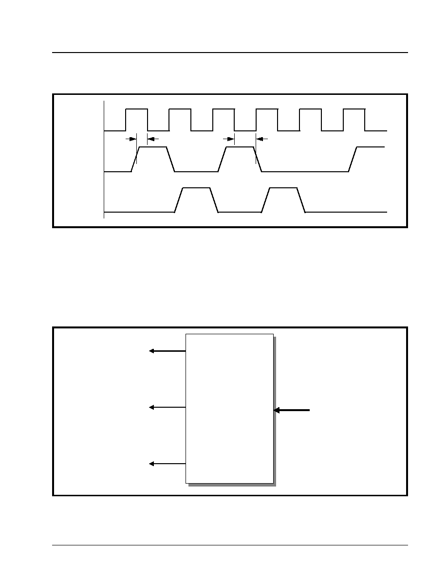
·Á
·Á
·Á
·Á
XRT7250
DS3/E3 FRAMER IC
REV. 1.1.1
289
5.3.2
The Receive E3 Framer Block
The Receive E3 Framer block accepts decoded E3
data from the Receive E3 LIU Interface block, and
routes data to the following destinations.
∑ The Receive Payload Data Output Interface Block
∑ The Receive Overhead Data Output Interface
Block.
∑ The Receive E3 HDLC Controller Block
Figure 135 presents a simple illustration of the Re-
ceive E3 Framer block along with the associated
paths to the other functional blocks within the Framer
chip.
Once the HDB3 (or AMI) encoded data has been de-
coded into a binary data-stream, the Receive E3
Framer block will use portions of this data-stream in
order to synchronize itself to the remote terminal
equipment. At any given time, the Receive E3 Fram-
er block will be operating in one of two modes.
F
IGURE
134. W
AVEFORM
/T
IMING
R
ELATIONSHIP
BETWEEN
R
X
L
INE
C
LK
, R
X
POS
AND
R
X
NEG - W
HEN
R
X
POS
AND
R
X
NEG
ARE
TO
BE
SAMPLED
ON
THE
FALLING
EDGE
OF
R
X
L
INE
C
LK
RxLineClk
RxPOS
RxNEG
t40
t41
F
IGURE
135. A S
IMPLE
I
LLUSTRATION
OF
THE
R
ECEIVE
E3 F
RAMER
B
LOCK
AND
THE
A
SSOCIATED
P
ATHS
TO
THE
O
THER
F
UNCTIONAL
B
LOCKS
Receive E3 Framer
Block
Receive E3 Framer
Block
To Receive E3 HDLC
Buffer
Receive Overhead Data
Output Interface
Receive Payload Data
Output Interface
From Receive E3
LIU Interface Block

XRT7250
·Á
·Á
·Á
·Á
DS3/E3 FRAMER IC
REV. 1.1.1
290
∑ The Frame Acquisition Mode: In this mode, the
Receive E3 Framer block is trying to acquire syn-
chronization with the incoming E3 frame, or
∑ The Frame Maintenance Mode: In this mode, the
Receive E3 Framer block is trying to maintain frame
synchronization with the incoming E3 Frames.
Figure 136 presents a State Machine diagram that
depicts the Receive E3 Framer block's E3/ITU-T
G.751 Frame Acquisition/Maintenance Algorithm.
5.3.2.1
The Framing Acquisition Mode
The Receive E3 Framer block is considered to be op-
erating in the Frame Acquisition Mode, if it is operat-
ing in any one of the following states within the E3
Frame Acquisition/Maintenance Algorithm per
Figure 136.
∑ FAS Pattern Search State
∑ FAS Pattern Verification State
∑ OOF Condition State
∑ LOF Condition State
Each of these Framing Acquisition states, within the
Receive E3 Framer Framing Acquisition/Maintenance
State Machine are discussed below.
The FAS Pattern Search State
When the Receive E3 Framer block is first powered
up, it will be operating in the FAS Pattern Search
state. While the Receive E3 Framer is operating in
this state, it will be performing a bit-by-bit search for
the FAS (Framing Alignment Signal) pattern, of
"1111010000". Figure 137, which presents an illus-
tration of the E3, ITU-T G.751 Framing Format, indi-
cates that this framing alignment signal will occur at
the beginning of each E3 frame.
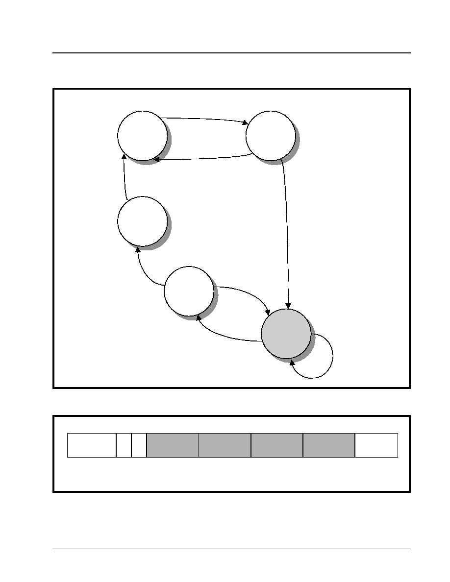
·Á
·Á
·Á
·Á
XRT7250
DS3/E3 FRAMER IC
REV. 1.1.1
291
When the Receive E3 Framer block detects the FAS
pattern, it will then transition over to the FAS Pattern
Verification state, per Figure 137.
The FAS Pattern Verification State
Once the Receive E3 Framer block has detected an
"1111010000" pattern, it must verify that this pattern
is indeed the FAS pattern and not some other set of
bits, within the E3 frame, mimicking the FAS Pattern.
F
IGURE
136. T
HE
S
TATE
M
ACHINE
D
IAGRAM
FOR
THE
R
ECEIVE
E3 F
RAMER
E3 F
RAME
A
CQUISITION
/M
AINTENANCE
A
LGORITHM
FAS
Pattern
Search
FAS
Pattern
Verification
In Frame
OOF
Condition
LOF
Condition
FAS pattern is
detected once
FAS Pattern is
verified once
FAS Pattern is
not detected
4 consecutive
In-valid Frames
3 consecutive
Valid Frames
8 or 24 framing periods
of operating in the
OOF condition
(user-selectable)
Frame Maintenance
Mode
F
IGURE
137. I
LLUSTRATION
OF
THE
E3, ITU-T G.751 F
RAMING
F
ORMAT
Frame
Alignment
Signal
A
N
Data
Data
Data
Data
BIP-4
if Selected
1 10 11 12 384 385 768 769 1152 1153 1532 1536
Framing Alignment Signal Pattern = 1111010000

XRT7250
·Á
·Á
·Á
·Á
DS3/E3 FRAMER IC
REV. 1.1.1
292
Hence, the purpose of the FAS Pattern Verification
state.
When the Receive E3 Framer block enters this state,
it will then quit performing its bit-by-bit search for the
Frame Alignment Signaling bits. Instead, the Receive
E3 Framer block will read in the 10 bits that occur
1536 bit (e.g., one E3 frame period later) after the
candidate FAS pattern was first detected. If these ten
bits match the assigned values for the FAS Pattern
octets, then the Receive E3 Framer block will con-
clude that it has found the FAS pattern and will then
transition to the In-Frame state. However, if these two
bytes do not match the assigned values for the FAS
pattern then the Receive E3 Framer block will con-
cluded that it has been fooled by data mimicking the
Frame Alignment bytes, and will transition back to the
FAS Pattern Search state.
In Frame State
Once the Receive E3 Framer block enters the In-
Frame state, then it will cease performing Frame Ac-
quisition functions, and will proceed to perform Fram-
ing Maintenance functions. Therefore, the operation
of the Receive E3 Framer block, while operating in
the In-Frame state, can be found in Section 4.3.2.2
(The Framing Maintenance Mode).
OOF (Out of Frame) Condition State
If the Receive E3 Framer while operating in the In-
Frame state detects four (4) consecutive frames,
which do not have the valid Frame Alignment Signal-
ing (FAS) patterns, then it will transition into the OOF
Condition State. The Receive E3 Framer block's op-
eration, while in the OOF condition state is a unique
mix of Framing Maintenance and Framing Acquisition
operation. The Receive E3 Framer block will exhibit
some Framing Acquisition characteristics by attempt-
ing to locate (once again) the FAS pattern. However,
the Receive E3 Framer block will also exhibit some
Frame Maintenance behavior by still using the most
recent frame synchronization for its overhead bits and
payload bits processing.
The Receive E3 Framer block will inform the Micro-
processor/Microcontroller of its transition from the In-
Frame state to the OOF Condition state, by generat-
ing a Change in OOF Condition Interrupt. When this
occurs, Bit 3 (OOF Interrupt Status), within the Rx E3
Interrupt Status Register - 1, will be set to "1", as de-
picted below.
The Receive E3 Framer block will also inform the ex-
ternal circuitry of its transition into the OOF Condition
state, by toggling the RxOOF output pin "High".
If the Receive E3 Framer block is capable of finding
the FAS pattern within a user-selectable number of
E3 frame periods, then it will transition back into the
In-Frame state. The Receive E3 Framer block will
then inform the Microprocessor/Microcontroller of its
transition back into the In-Frame state by generating
the Change in OOF Condition Interrupt.
However, if the Receive E3 Framer block resides in
the OOF Condition state for more than this user-se-
lectable number of E3 frame periods, then it will auto-
matically transition to the LOF (Loss of Frame) Condi-
tion state.
The user can select this user-selectable number of
E3 frame periods that the Receive E3 Framer block
will remain in the OOF Condition state by writing the
appropriate value into Bit 7 (RxLOF Algo) within the
Rx E3 Configuration & Status Register, as depicted
below.
RXE3 INTERRUPT STATUS REGISTER - 1 (ADDRESS = 0X14)
B
IT
7
B
IT
6
B
IT
5
B
IT
4
B
IT
3
B
IT
2
B
IT
1
B
IT
0
Not Used
COFA
Interrupt
Status
OOF
Interrupt
Status
LOF
Interrupt
Status
LOS
Interrupt
Status
AIS
Interrupt
Status
RO
RO
RO
RUR
RUR
RUR
RUR
RUR
0
0
0
0
0
0
0
0
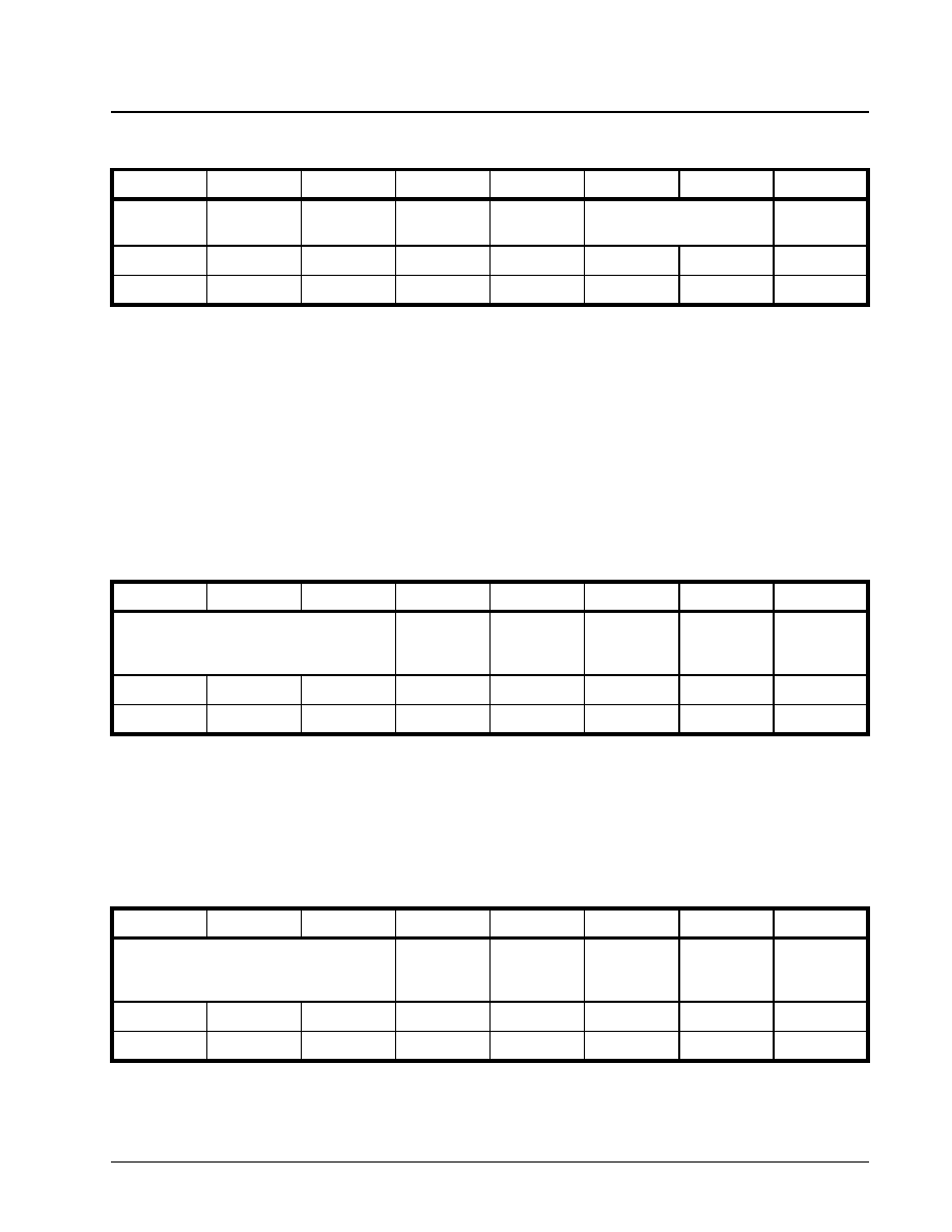
·Á
·Á
·Á
·Á
XRT7250
DS3/E3 FRAMER IC
REV. 1.1.1
293
Writing a "0" into this bit-field causes the Receive E3
Framer block to reside in the OOF Condition state for
at most 24 E3 frame periods. Writing a "1" into this
bit-field causes the Receive E3 Framer block to reside
in the OOF Condition state for at most 8 E3 frame pe-
riods.
LOF (Loss of Framing) Condition State
If the Receive E3 Framer block enters the LOF Condi-
tion state, then the following things will happen.
∑ The Receive E3 Framer block will discard the most
recent frame synchronization and,
∑ The Receive E3 Framer block will make an uncon-
ditional transition to the FAS Pattern Search state.
∑ The Receive E3 Framer block will notify the Micro-
processor/Microcontroller of its transition to the
LOF Condition state, by generating the Change in
LOF Condition interrupt. When this occurs, Bit 2
(LOF Interrupt Status), within the Rx E3 Interrupt
Status Register - 1 will be set to "1", as depicted
below.
Finally, the Receive E3 Framer block will also inform
the external circuitry of this transition to the LOF Con-
dition state by toggling the RxLOF output pin "High".
5.3.2.2
The Framing Maintenance Mode
Once the Receive E3 Framer block enters the In-
Frame state, then it will notify the Microprocessor/Mi-
crocontroller of this fact by generating both the
Change in OOF Condition and Change in LOF Condi-
tion Interrupts. When this happens, bits 2 and 3 (LOF
Interrupt Status and OOF Interrupt Status) will be set
to "1", as depicted below.
Additionally, the Receive E3 Framer block will inform
the external circuitry of its transition to the In-Frame
state by toggling both the RxOOF and RxLOF output
pins "Low".
Finally, the Receive E3 Framer block will negate both
the RxOOF and the RxLOF bit-fields within the Rx E3
Configuration & Status Register, as depicted below.
RXE3 CONFIGURATION & STATUS REGISTER - 2 (ADDRESS = 0X11)
B
IT
7
B
IT
6
B
IT
5
B
IT
4
B
IT
3
B
IT
2
B
IT
1
B
IT
0
RxLOF
Algo
RxLOF
RxOOF
RxLOS
RxAIS
Not Used
RxFERF
R/W
RO
RO
RO
RO
RO
RO
RO
0
1
1
0
0
1
1
1
RXE3 INTERRUPT STATUS REGISTER - 1 (ADDRESS = 0X14)
B
IT
7
B
IT
6
B
IT
5
B
IT
4
B
IT
3
B
IT
2
B
IT
1
B
IT
0
Not Used
COFA
Interrupt
Status
OOF
Interrupt
Status
LOF
Interrupt
Status
LOS
Interrupt
Status
AIS
Interrupt
Status
RO
RO
RO
RUR
RUR
RUR
RUR
RUR
0
0
0
0
0
1
0
0
RXE3 INTERRUPT STATUS REGISTER - 1 (ADDRESS = 0X14)
B
IT
7
B
IT
6
B
IT
5
B
IT
4
B
IT
3
B
IT
2
B
IT
1
B
IT
0
Not Used
COFA
Interrupt
Status
OOF
Interrupt
Status
LOF
Interrupt
Status
LOS
Interrupt
Status
AIS
Interrupt
Status
RO
RO
RO
RUR
RUR
RUR
RUR
RUR
0
0
0
0
1
1
0
0
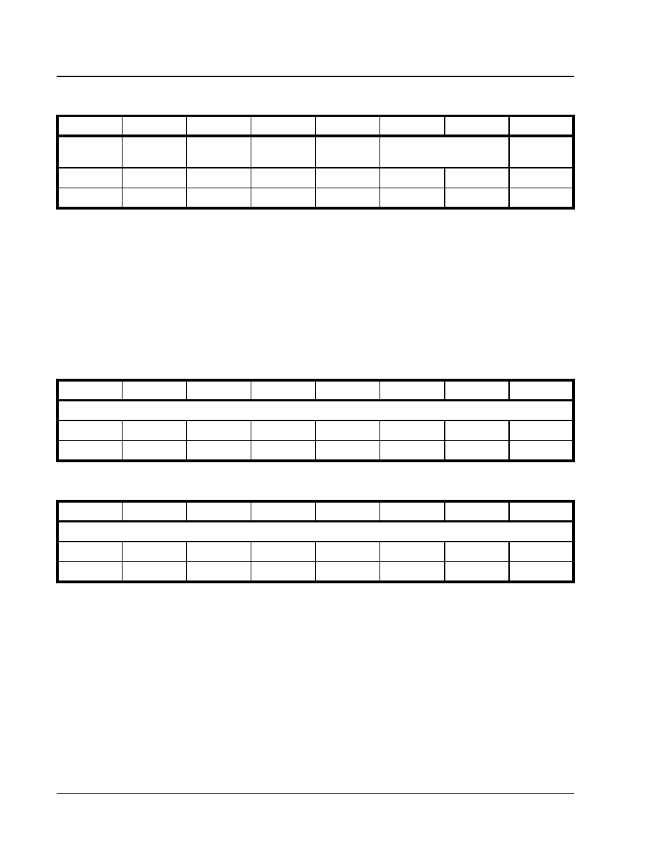
XRT7250
·Á
·Á
·Á
·Á
DS3/E3 FRAMER IC
REV. 1.1.1
294
When the Receive E3 Framer block is operating in the
In-Frame state, it will then begin to perform Frame
Maintenance operations, where it will continue to ver-
ify that the Frame Alignment signal (FAS pattern) is
present, and at its proper location. While the Receive
E3 Framer block is operating in the Frame Mainte-
nance Mode, it will declare an Out-of-Frame (OOF)
Condition if it detects an invalid FAS pattern in four
consecutive frames.
Since the Receive E3 Framer block requires the de-
tection of an invalid FAS pattern in four consecutive
frames, in order for it to transition to the OOF Condi-
tion state, it can tolerate some errors in the Framing
Alignment bytes, and still remain in the In-Frame
state. However, each time the Receive E3 Framer
block detects an error in the FAS pattern, it will incre-
ment the PMON Framing Error Event Count Regis-
ters (Address = 0x52 and 0x53). The bit-format for
these two registers are depicted below.
5.3.2.3
Forcing a Reframe via Software Com-
mand
The XRT7250 Framer IC permits the user to com-
mand a reframe procedure with the Receive E3 Fram-
er block via software command. If the user writes a
"1" into Bit 0 (Reframe) within the I/O Control Register
(Address = 0x01), as depicted below, then the Re-
ceive E3 Framer block will be forced into the FAS Pat-
tern Search state, per Figure 138., and will begin its
search for the FAS Pattern.
RXE3 CONFIGURATION & STATUS REGISTER - 2 (ADDRESS = 0X11)
B
IT
7
B
IT
6
B
IT
5
B
IT
4
B
IT
3
B
IT
2
B
IT
1
B
IT
0
RxLOF
Algo
RxLOF
RxOOF
RxLOS
RxAIS
Not Used
RxFERF
R/W
RO
RO
RO
RO
RO
RO
RO
0
0
0
0
0
1
1
1
PMON FRAMING BIT/BYTE ERROR COUNT REGISTER - MSB (ADDRESS = 0X52)
B
IT
7
B
IT
6
B
IT
5
B
IT
4
B
IT
3
B
IT
2
B
IT
1
B
IT
0
Framing Bit/Byte Error Count - High Byte
RUR
RUR
RUR
RUR
RUR
RUR
RUR
RUR
0
0
0
0
0
0
0
0
PMON FRAMING BIT/BYTE ERROR COUNT REGISTER - LSB (ADDRESS = 0X53)
B
IT
7
B
IT
6
B
IT
5
B
IT
4
B
IT
3
B
IT
2
B
IT
1
B
IT
0
Framing Bit/Byte Error Count - Low Byte
RUR
RUR
RUR
RUR
RUR
RUR
RUR
RUR
0
0
0
0
0
0
0
0

·Á
·Á
·Á
·Á
XRT7250
DS3/E3 FRAMER IC
REV. 1.1.1
295
)
The Framer IC will respond to this command by doing
the following.
1. Asserting both the RxOOF and RxLOF output
pins.
2. Generating both the Change in OOF Status and
the Change in LOF Status interrupts to the Micro-
processor.
3. Asserting both the RxLOF and RxOOF bit-fields
within the Rx E3 Configuration & Status Register,
as depicted below.
5.3.2.4
Performance Monitoring of the Frame
Synchronization Section, within the Receive E3
Framer block
The user can monitor the number of FAS pattern er-
rors that have been detected by the Receive E3
Framer block. This is accomplished by periodically
reading the PMON Framing Bit/Byte Error Event
Count Registers (Address = 0x52 and 0x53). The
byte format of these registers are presented below.
5.3.2.5
The RxOOF and RxLOF output pin.
The user can roughly determine the current framing
state that the Receive E3 Framer block is operating in
by reading the logic state of the RxOOF and the Rx-
LOF output pins. Table 61 presents the relationship
between the state of the RxOOF and RxLOF output
pins, and the Framing State of the Receive E3 Framer
block.
5.3.2.6
E3 Receive Alarms
5.3.2.7
The Loss of Signal (LOS) Alarm
Declaring an LOS Condition
The Receive E3 Framer block will declare a Loss of
Signal (LOS) Condition, when it detects 32 consecu-
tive incoming "0's" via the RxPOS and RxNEG input
pins or if the ExtLOS input pin (from the XRT7300
DS3/E3/STS-1 LIU IC) is asserted. The Receive E3
Framer block will indicate that it is declaring an LOS
condition by.
I/O CONTROL REGISTER (ADDRESS = 0X01)
B
IT
7
B
IT
6
B
IT
5
B
IT
4
B
IT
3
B
IT
2
B
IT
1
B
IT
0
Disable
TxLOC
LOC
Disable
RxLOC
AMI/
ZeroSup*
Unipolar/
Bipolar*
TxLine
Clk
Invert
RxLine
Clk
Invert
Reframe
R/W
RO
R/W
R/W
R/W
R/W
R/W
R/W
1
0
1
0
0
0
0
1
RXE3 CONFIGURATION & STATUS REGISTER - 2 (ADDRESS = 0X11)
B
IT
7
B
IT
6
B
IT
5
B
IT
4
B
IT
3
B
IT
2
B
IT
1
B
IT
0
RxLOF
Algo
RxLOF
RxOOF
RxLOS
RxAIS
Not Used
RxFERF
R/W
RO
RO
RO
RO
RO
RO
RO
0
1
1
0
0
1
1
0
T
ABLE
61: T
HE
R
ELATIONSHIP
BETWEEN
THE
L
OGIC
S
TATE
OF
THE
R
X
OOF
AND
R
X
LOF
OUTPUT
PINS
,
AND
THE
F
RAMING
S
TATE
OF
THE
R
ECEIVE
E3 F
RAMER
BLOCK
R
X
LOF
R
X
OOF
F
RAMING
S
TATE
OF
THE
R
ECEIVE
E3 F
RAMER
BLOCK
0
0
In Frame
0
1
OOF Condition (The Receive E3 Framer block is operating in the 3ms OOF period).
1
0
Invalid
1
1
LOF Condition

XRT7250
·Á
·Á
·Á
·Á
DS3/E3 FRAMER IC
REV. 1.1.1
296
∑ Asserting the RxLOS output pin (e.g., toggling it
"High").
∑ Setting Bit 4 (RxLOS) of the Rx E3 Configuration &
Status Register to "1" as depicted below.
∑ The Receive E3 Framer block will generate a
Change in LOS Condition interrupt request. Upon
generating this interrupt request, the Receive E3
Framer block will assert Bit 1 (LOS Interrupt Status
within the Rx E3 Framer Interrupt Status Register -
1, as depicted below.
Clearing the LOS Condition
The Receive E3 Framer block will clear the LOS con-
dition when it encounters a stream of 32 bits that
does not contain a string of 4 consecutive zeros.
When the Receive E3 Framer block clears the LOS
condition, then it will notify the Microprocessor and
the external circuitry of this occurrence by:
∑ Generating the Change in LOS Condition Interrupt
to the Microprocessor.
∑ Clearing Bit 4 (RxLOS) within the Rx E3 Configura-
tion & Status Register, as depicted below.
∑ Clear the RxLOS output pin (e.g., toggle it "Low").
5.3.2.8
The AIS (Alarm Indication Status) Con-
dition
Declaring the AIS Condition
The Receive E3 Framer block will identify and declare
an AIS condition, if it detects an All Ones" pattern in
the incoming E3 data stream. More specifically, the
Receive E3 Framer block will declare an AIS Condi-
tion if 7 or less "0's" are detected in each of 2 consec-
utive E3 frames.
If the Receive E3 Framer block declares an AIS Con-
dition, then it will do the following.
∑ Generate the Change in AIS Condition Interrupt to
the Microprocessor. Hence, the Receive E3
Framer block will assert Bit 0 (AIS Interrupt Status)
within the Rx E3 Framer Interrupt Status register -
1, as depicted below.
RXE3 CONFIGURATION & STATUS REGISTER - 2 (ADDRESS = 0X11)
B
IT
7
B
IT
6
B
IT
5
B
IT
4
B
IT
3
B
IT
2
B
IT
1
B
IT
0
RxLOF
Algo
RxLOF
RxOOF
RxLOS
RxAIS
Not Used
RxFERF
R/W
RO
RO
RO
RO
RO
RO
RO
0
1
1
1
0
0
0
0
RXE3 INTERRUPT STATUS REGISTER - 1 (ADDRESS = 0X14)
B
IT
7
B
IT
6
B
IT
5
B
IT
4
B
IT
3
B
IT
2
B
IT
1
B
IT
0
Not Used
COFA
Interrupt
Status
OOF
Interrupt
Status
LOF
Interrupt
Status
LOS
Interrupt
Status
AIS
Interrupt
Status
RO
RO
RO
RUR
RUR
RUR
RUR
RUR
0
0
0
0
0
0
1
0
RXE3 CONFIGURATION & STATUS REGISTER - 2 (ADDRESS = 0X11)
B
IT
7
B
IT
6
B
IT
5
B
IT
4
B
IT
3
B
IT
2
B
IT
1
B
IT
0
RxLOF
Algo
RxLOF
RxOOF
RxLOS
RxAIS
Not Used
RxFERF
R/W
RO
RO
RO
RO
RO
RO
RO
0
1
1
0
0
1
1
1

·Á
·Á
·Á
·Á
XRT7250
DS3/E3 FRAMER IC
REV. 1.1.1
297
∑ Assert the RxAIS output pin.
∑ Set Bit 3 (RxAIS) within the Rx E3 Configuration &
Status Register, as depicted below.
Clearing the AIS Condition
The Receive E3 Framer block will clear the AIS condi-
tion when it detects two consecutive E3 frames, with
eight or more "zeros" in the incoming data stream.
The Receive E3 Framer block will inform the Micro-
processor that the AIS Condition has been cleared
by:
∑ Generating the Change in AIS Condition Interrupt
to the Microprocessor. Hence, the Receive E3
Framer block will assert Bit 0 (AIS Interrupt Status)
within the Rx E3 Framer Interrupt Status Register -
1.
∑ Clearing the RxAIS output pin (e.g., toggling it
"Low").
∑ Setting the RxAIS bit-field, within the Rx E3 Config-
uration & Status Register to "0", as depicted below.
5.3.2.9
The Far-End-Receive Failure (FERF)
Condition
Declaring the FERF Condition
The Receive E3 Framer block will declare a Far-End
Receive Failure (FERF) condition if it detects a user-
selectable number of consecutive incoming E3
frames, with the "A" bit-field set to "1".
This User-selectable number of E3 frames is either 3
or 5, depending upon the value that has been written
into Bit 4 (RxFERF Algo) within the Rx E3 Configura-
tion & Status Register, as depicted below.
RXE3 INTERRUPT STATUS REGISTER - 1 (ADDRESS = 0X14)
B
IT
7
B
IT
6
B
IT
5
B
IT
4
B
IT
3
B
IT
2
B
IT
1
B
IT
0
Not Used
COFA
Interrupt
Status
OOF
Interrupt
Status
LOF
Interrupt
Status
LOS
Interrupt
Status
AIS
Interrupt
Status
RO
RO
RO
RUR
RUR
RUR
RUR
RUR
0
0
0
0
0
0
0
1
RXE3 CONFIGURATION & STATUS REGISTER - 2 (ADDRESS = 0X11)
B
IT
7
B
IT
6
B
IT
5
B
IT
4
B
IT
3
B
IT
2
B
IT
1
B
IT
0
RxLOF
Algo
RxLOF
RxOOF
RxLOS
RxAIS
Not Used
RxFERF
R/W
RO
RO
RO
RO
RO
RO
RO
0
1
1
0
1
1
1
1
RXE3 CONFIGURATION & STATUS REGISTER - 2 (ADDRESS = 0X11)
B
IT
7
B
IT
6
B
IT
5
B
IT
4
B
IT
3
B
IT
2
B
IT
1
B
IT
0
RxLOF
Algo
RxLOF
RxOOF
RxLOS
RxAIS
Not Used
RxFERF
R/W
RO
RO
RO
RO
RO
RO
RO
0
1
1
0
1
0
0
X

XRT7250
·Á
·Á
·Á
·Á
DS3/E3 FRAMER IC
REV. 1.1.1
298
Writing a "0" into this bit-field causes the Receive E3
Framer block to declare a FERF condition, if it detects
3 consecutive incoming E3 frames, that have the "A"
bit set to "1".
Writing a "1" into this bit-field causes the Receive E3
Framer block to declare a FERF condition, if it detects
5 consecutive incoming E3 frames, that have the "A"
bit set to "1".
Whenever the Receive E3 Framer block declares a
FERF condition, then it will do the following.
∑ Generate a Change in FERF Condition interrupt to
the MIcroprocessor. Hence, the Receive E3
Framer block will assert Bit 3 (FERF Interrupt Sta-
tus) within the Rx E3 Framer Interrupt Status regis-
ter - 2, as depicted below.
∑ Set the RxFERF bit-field, within the Rx E3 Configu-
ration/Status Register to "1", as depicted below.
Clearing the FERF Condition
The Receive E3 Framer block will clear the FERF
condition once it has received a User-Selectable
number of E3 frames with the "A" bit-field being set to
"0" (e.g., no FERF condition). This User-Selectable
number of E3 frames is either 3 or 5 depending upon
the value that has been written into Bit 4 (RxFERF Al-
go) of the Rx E3 Configuration/Status Register, as
discussed above.
Whenever the Receive E3 Framer clears the FERF
status, then it will do the following:
1. Generate a Change in the FERF Status Interrupt
to the Microprocessor.
2. Clear the Bit 0 (RxFERF) within the Rx E3 Con-
figuration & Status register, as depicted below.
RXE3 CONFIGURATION & STATUS REGISTER - 1 G.751 (ADDRESS = 0X10)
B
IT
7
B
IT
6
B
IT
5
B
IT
4
B
IT
3
B
IT
2
B
IT
1
B
IT
0
Reserved
RxFERF
Algo
Reserved
RxBIP4
RO
RO
RO
R/W
RO
RO
RO
R/W
0
0
0
0
0
0
0
0
RXE3 INTERRUPT STATUS REGISTER - 2 (ADDRESS = 0X15)
B
IT
7
B
IT
6
B
IT
5
B
IT
4
B
IT
3
B
IT
2
B
IT
1
B
IT
0
Not Used
FERF
Interrupt
Status
BIP-4
Error
Interrupt
Status
Framing
Error
Interrupt
Status
Not Used
RO
RO
RO
RO
RUR
RUR
RUR
RUR
0
0
0
0
1
0
0
0
RXE3 CONFIGURATION & STATUS REGISTER - 2 (ADDRESS = 0X11)
B
IT
7
B
IT
6
B
IT
5
B
IT
4
B
IT
3
B
IT
2
B
IT
1
B
IT
0
RxLOF
Algo
RxLOF
RxOOF
RxLOS
RxAIS
Not Used
RxFERF
R/W
RO
RO
RO
RO
RO
RO
RO
0
1
1
0
0
0
0
0
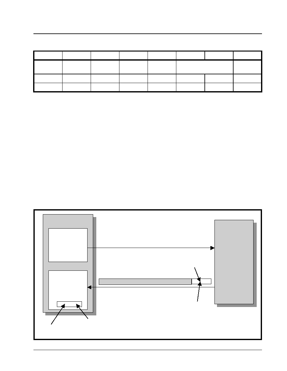
·Á
·Á
·Á
·Á
XRT7250
DS3/E3 FRAMER IC
REV. 1.1.1
299
5.3.2.10 Error Checking of the Incoming E3
Frames
The Receive E3 Framer block can be configured to
performs error-checking on the incoming E3 frame
data that it receives from the Remote Terminal Equip-
ment. If configured accordingly, the Receive E3
Framer block will performs this error-checking by
computing the BIP-4 value of an incoming E3 frame.
Once the Receive E3 Framer block has obtained this
value, it will compare this value with that of the BIP-4
value that it receives, within the very next E3 frame. If
the locally computed BIP-4 value matches the EM
byte of the corresponding E3 frame, then the Receive
E3 Framer block will conclude that this particular
frame has been properly received. The Receive E3
Framer block will then inform the Remote Terminal
Equipment of this fact by having the Local Terminal
Equipment Transmit E3 Framer block send the Re-
mote Terminal an E3 frame, with the "A" bit-field, set
to "0".
This procedure is illustrated in Figure 138 and
Figure 139, below.
Figure 138 illustrates the Local Receive E3 Framer
receiving an error-free E3 frame. In this figure, the lo-
cally computed BIP-4 value of "0xA" matches that re-
ceived from the Remote Terminal, within the EM byte-
field. Figure 139 illustrates the subsequent action of
the Local Transmit E3 Framer block, which will trans-
mit an E3 frame, with the A bit-field set to "0", to the
Remote Terminal. This signaling indicates that the
Local Receive E3 Framer has received an error-free
E3 frame.
RXE3 CONFIGURATION & STATUS REGISTER - 2 (ADDRESS = 0X11)
B
IT
7
B
IT
6
B
IT
5
B
IT
4
B
IT
3
B
IT
2
B
IT
1
B
IT
0
RxLOF
Algo
RxLOF
RxOOF
RxLOS
RxAIS
Not Used
RxFERF
R/W
RO
RO
RO
RO
RO
RO
RO
0
1
1
0
0
1
1
1
F
IGURE
138. I
LLUSTRATION
OF
THE
L
OCAL
R
ECEIVE
E3 F
RAMER
BLOCK
,
RECEIVING
AN
E3 F
RAME
(
FROM
THE
R
EMOTE
T
ERMINAL
)
WITH
A
CORRECT
BIP-4 V
ALUE
.
Transmit E3
Framer
Receive E3
Framer
Local Terminal
Remote
Terminal
BIP-4 Nibble
Locally Calculated
BIP-4 Nibble
0xA
0xA

XRT7250
·Á
·Á
·Á
·Á
DS3/E3 FRAMER IC
REV. 1.1.1
300
However, if the locally computed BIP-4 value does not
match the BIP-4 value of the corresponding E3 frame,
then the Receive E3 Framer block will do the follow-
ing.
∑ It will inform the Remote Terminal of this fact by
having the Local Transmit E3 Framer block send the
Remote Terminal an E3 frame, with the "A" bit-field
set to "1". This phenomenon is illustrated below in
Figure 140 and Figure 141.
Figure 140 illustrates the Local Receive E3 Framer
receiving an errored E3 frame. In this figure, the Lo-
cal Receive E3 Frame block is receiving an E3 frame
with an BIP-4 containing the value "0xA". This value
does not match the locally computed BIP-4 value of
"0xB". Consequently, there is an error in the previous
E3 frame.
Figure 141 illustrates the subsequent action of the
Local Transmit E3 Framer block, which will transmit
an E3 frame, with the A bit-field set to "1" to the Re-
mote Terminal. This signaling indicates that the Local
Receive E3 Framer block has received an errored E3
frame.
F
IGURE
139. I
LLUSTRATION
OF
THE
L
OCAL
R
ECEIVE
E3 F
RAMER
BLOCK
,
TRANSMITTING
AN
E3 F
RAME
(
TO
THE
R
EMOTE
T
ERMINAL
)
WITH
THE
"A"
BIT
SET
TO
"0"
Transmit E3
Framer
Receive E3
Framer
Local Terminal
Remote
Terminal
A Bit
Value = 0
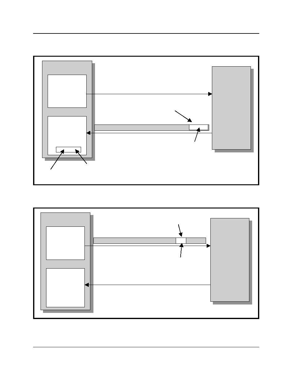
·Á
·Á
·Á
·Á
XRT7250
DS3/E3 FRAMER IC
REV. 1.1.1
301
In additional to the FEBE bit-field signaling, the Re-
ceive E3 Framer block will generate the BIP-4 Error
Interrupt to the Microprocessor. Hence, it will set bit 2
(BIP-8 Error Interrupt Status) to "1", as depicted be-
low.
F
IGURE
140. I
LLUSTRATION
OF
THE
L
OCAL
R
ECEIVE
E3 F
RAMER
BLOCK
,
RECEIVING
AN
E3 F
RAME
(
FROM
THE
R
EMOTE
T
ERMINAL
)
WITH
AN
INCORRECT
BIP-4
VALUE
.
Transmit E3
Framer
Receive E3
Framer
Local Terminal
Remote
Terminal
BIP-4 Nibble
Locally Calculated
BIP-4 Nibble
0xA
0xB
F
IGURE
141. I
LLUSTRATION
OF
THE
L
OCAL
R
ECEIVE
E3 F
RAMER
BLOCK
,
TRANSMITTING
AN
E3 F
RAME
(
TO
THE
R
EMOTE
T
ERMINAL
)
WITH
THE
"A"
BIT
-
FIELD
SET
TO
"1"
Transmit E3
Framer
Receive E3
Framer
Local Terminal
Remote
Terminal
A Bit
Value = 1

XRT7250
·Á
·Á
·Á
·Á
DS3/E3 FRAMER IC
REV. 1.1.1
302
Finally, the Receive E3 Framer block will increment
the PMON Parity Error Count registers. The byte for-
mat of these registers are presented below.
The user can determine the number of BIP-4 Errors
that have been detected by the Receive E3 Framer
block, since the last read of these registers. These
registers are reset-upon-read.
Configuring the XRT7250 Framer IC to support
BIP-4 Error Detection
In order to perform BIP-4 checking of each E3 frame,
the user must configure the XRT7250 Framer IC ac-
cordingly, by executing the following steps.
1. Configure the Transmit Section (of the XRT7250
Framer IC) to insert the BIP-4 value into the out-
bound E3 frames. This is accomplished by writ-
ing a "1" into bit-field 7 (Tx BIP-4 Enable) within
the TxE3 Configuration Register, as illustrated
below.
RXE3 INTERRUPT STATUS REGISTER - 2 (ADDRESS = 0X15)
B
IT
7
B
IT
6
B
IT
5
B
IT
4
B
IT
3
B
IT
2
B
IT
1
B
IT
0
Not Used
FERF
Interrupt
Status
BIP-4
Error
Interrupt
Status
Framing
Error
Interrupt
Status
Not Used
RO
RO
RO
RO
RUR
RUR
RUR
RUR
0
0
0
0
0
1
0
0
PMON PARITY ERROR COUNT REGISTER - MSB (ADDRESS = 0X54)
B
IT
7
B
IT
6
B
IT
5
B
IT
4
B
IT
3
B
IT
2
B
IT
1
B
IT
0
Parity Error Count - High Byte
RUR
RUR
RUR
RUR
RUR
RUR
RUR
RUR
0
0
0
0
0
0
0
0
PMON PARITY ERROR COUNT REGISTER - LSB (ADDRESS = 0X55)
B
IT
7
B
IT
6
B
IT
5
B
IT
4
B
IT
3
B
IT
2
B
IT
1
B
IT
0
Parity Error Count - Low Byte
RUR
RUR
RUR
RUR
RUR
RUR
RUR
RUR
0
0
0
0
0
0
0
0
TXE3 CONFIGURATION REGISTER (ADDRESS = 0X30)
B
IT
7
B
IT
6
B
IT
5
B
IT
4
B
IT
3
B
IT
2
B
IT
1
B
IT
0
Tx
BIP-4
Enable
TxASourceSel[1:0]
TxNSourceSel[1:0]
Tx AIS
Enable
Tx LOS
Enable
Tx FAS
Source
Select
R/W
R/W
R/W
R/W
R/W
R/W
R/W
R/W
1
0
0
0
0
0
0
0

·Á
·Á
·Á
·Á
XRT7250
DS3/E3 FRAMER IC
REV. 1.1.1
303
2. Enable the BIP-4 Error Interrupt. This is accom-
plished by writing a "1" into bit-field 2 (BIP-4 Error
Interrupt Enable) within the RxE3 Interrupt
Enable Register, as illustrated below.
After doing this, the XRT7250 Framer IC will generate
an interrupt to the Microprocessor/Microcontroller
anytime the Receive Section detects a BIP-4 error.
5.3.3
The Receive HDLC Controller Block
The Receive E3 HDLC Controller block can be used
to receive message-oriented signaling (MOS) type
data link messages from the remote terminal equip-
ment.
The MOS types of HDLC message processing is dis-
cussed in detail below.
The Message Oriented Signaling (e.g., LAP-D)
Processing via the Receive E3 HDLC Controller
block
The LAPD Receiver (within the Receive E3 HDLC
Controller block) allows the user to receive PMDL
messages from the remote terminal equipment, via
the inbound E3 frames. In this case, the inbound
message bits will be carried by the "N" bit-field within
each inbound E3 Frame. The remote LAPD Transmit-
ter will transmit a LAPD Message to the Local Receiv-
er via either the "N" bit within each E3 Frame. The
LAPD Receiver will receive and store the information
portion of the received LAPD frame into the Receive
LAPD Message Buffer, which is located at addresses:
0xDE through 0x135 within the on-chip RAM. The
LAPD Receiver has the following responsibilities.
∑ Framing to the incoming LAPD Messages
∑ Filtering out stuffed "0's" (within the information
payload)
∑ Storing the Frame Message into the Receive LAPD
Message Buffer
∑ Perform Frame Check Sequence (FCS) Verification
∑ Provide status indicators for
End of Message (EOM)
Flag Sequence Byte detected
Abort Sequence detected
Message Type
C/R Type
The occurrence of FCS Errors
The LAPD receiver's actions are facilitated via the fol-
lowing two registers.
∑ Rx E3 LAPD Control Register
∑ Rx E3 LAPD Status Register
Operation of the LAPD Receiver
The LAPD Receiver, once enabled, will begin search-
ing for the boundaries of the incoming LAPD mes-
sage. The LAPD Message Frame boundaries are de-
lineated via the Flag Sequence octets (0x7E), as de-
picted in Figure 142.
RXE3 INTERRUPT ENABLE REGISTER - 2 (ADDRESS = 0X13)
B
IT
7
B
IT
6
B
IT
5
B
IT
4
B
IT
3
B
IT
2
B
IT
1
B
IT
0
Not Used
FERF
Interrupt Enable
BIP-4 Error
Interrupt Enable
Framing Error
Interrupt Enable
Not Used
R/W
RO
RO
RO
R/W
R/W
R/W
RO
0
0
0
0
0
1
0
0
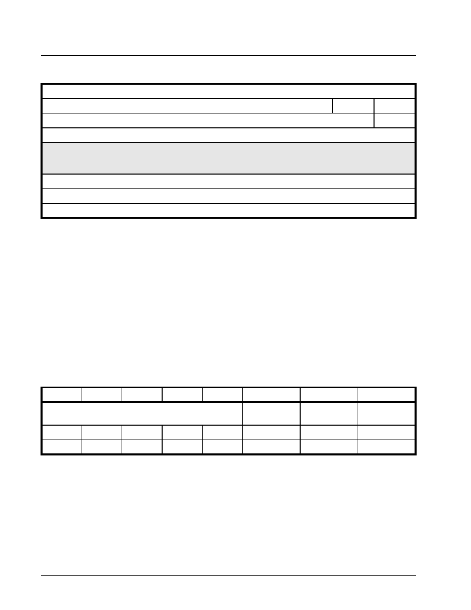
XRT7250
·Á
·Á
·Á
·Á
DS3/E3 FRAMER IC
REV. 1.1.1
304
Where: Flag Sequence = 0x7E
SAPI + CR + EA = 0x3C or 0x3E
TEI + EA = 0x01
Control = 0x03
The 16 bit FCS is calculated using CRC-16, x16 +
x12 + x5 + 1
The local µP (at the remote terminal), while assem-
bling the LAPD Message frame, will insert an addi-
tional byte at the beginning of the information (pay-
load) field. This first byte of the information field indi-
cates the type and size of the message being trans-
ferred. The value of this information field and the
corresponding message type/size follow:
CL Path Identification = 0x38 (76 bytes)
IDLE Signal Identification = 0x34 (76 bytes)
Test Signal Identification = 0x32 (76 bytes)
ITU-T Path Identification = 0x3F (82 bytes)
Enabling and Configuring the LAPD Receiver
Before the LAPD Receiver can begin to receive and
process incoming LAPD Message frames, the user
must do two things.
1. Enabling the LAPD Receiver
The LAPD Receiver must be enabled before it can
begin receiving and processing any LAPD Message
frames. The LAPD Receiver can be enabled by writ-
ing a "1" to Bit 2 (RxLAPD Enable) of the Rx E3 LAPD
Control Register, as indicated below.
)
Once the LAPD Receiver has been enabled, it will be-
gin searching for the Flag Sequence octet (0x7E), in
the "N" bit-fields within each incoming E3 frame.
When the LAPD Receiver finds the flag sequence
byte, it will assert the Flag Present bit (Bit 0) within
the Rx E3 LAPD Status Register, as depicted below.
F
IGURE
142. LAPD M
ESSAGE
F
RAME
F
ORMAT
Flag Sequence (8 bits)
SAPI (6-bits)
C/R
EA
TEI (7 bits)
EA
Control (8-bits)
76 or 82 Bytes of Information (Payload)
FCS - MSB
FCS - LSB
Flag Sequence (8-bits)
RXE3 LAPD CONTROL REGISTER (ADDRESS = 0X18
B
IT
7
B
IT
6
B
IT
5
B
IT
4
B
IT
3
B
IT
2
B
IT
1
B
IT
0
Not Used
RxLAPD
Enable
RxLAPD
Interrupt Enable
RxLAPD
Interrupt Enable
RO
RO
RO
RO
RO
R/W
R/W
RUR
0
0
0
0
0
0
0
0
·Á
·Á
·Á
·Á
XRT7250
DS3/E3 FRAMER IC
REV. 1.1.1
305
The receipt of the Flag Sequence octet can mean
one of two things.
1. This Flag Sequence byte may be marking the
beginning or end of an incoming LAPD Message
frame.
2. The Received Flag Sequence octet could be just
one of many Flag Sequence octets that are trans-
mitted via the E3 Transport Medium, during idle
periods between the transmission of LAPD Mes-
sage frames.
The LAPD Receiver will negate the Flag Present bit
as soon as it has received an octet that is something
other than the Flag Sequence octet. Once this hap-
pens, the LAPD Receiver should be receiving either
octet # 2 of the incoming LAPD Message, or an
ABORT Sequence (e.g., a string of seven or more
consecutive "1's"). If this next set of data is an
ABORT Sequence, then the LAPD Receiver will as-
sert the RxABORT bit-field (Bit 6) within the Rx E3
LAPD Status Register, as depicted below.
However, if this next octet is Octet #2 of an incoming
LAPD Message frame, then the LAPD Receiver is be-
ginning to receive a LAPD Message frame.
As the LAPD Receiver receives this LAPD Message
frame, it is reading in the LAPD Message frame oc-
tets, from "N" bit-fields within each incoming E3
frame. Secondly, it is reassembling these bits into a
LAPD Message frame.
Once the LAPD Receiver has received the complete
LAPD Message frame, then it will proceed to perform
the following five (5) steps.
1. PMDL Message Extraction
The LAPD Receiver will extract out the PMDL Mes-
sage, from the newly received LAPD Message frame.
The LAPD Receiver will then write this PMDL Mes-
sage into the Receive LAPD Message buffer within
the Framer IC.
N
OTE
: As the LAPD Receiver is extracting the PMDL Mes-
sage, from the newly received LAPD Message frame, the
LAPD Receiver will also check the PMDL data for the
occurrence of stuff bits (e.g., "0's" that were inserted into
the PMDL Message by the Remote LAPD Transmitter, in
order to prevent this data from mimicking the Flag
Sequence byte or an ABORT Sequence), and remove them
prior to writing the PMDL Message into the Receive LAPD
Message Buffer. Specifically, the LAPD Receiver will
search through the PMDL Message data and will remove
any "0" that immediately follows a string of 5 consecutive
"1's".
N
OTE
: For more information on how the LAPD Transmitter
inserted these stuff bits, please see Section 4.2.3.1.
2. FCS (Frame Check Sequence) Word Verification
The LAPD Receiver will compute the CRC-16 value
of the header octets and the PMDL Message octets,
within this LAPD Message frame and will compare it
with the value of the two octets, residing in the FCS
word-field of this LAPD Message frame. If the FCS
value of the newly received LAPD Message frame
matches the locally-computed CRC-16 value, then
the LAPD Receiver will conclude that it has received
this LAPD Message frame in an error-free manner.
However, if the FCS value does not match the locally-
computed CRC-16 value, then the LAPD Receiver
will conclude that this LAPD Message frame is erred.
RXE3 LAPD STATUS REGISTER (ADDRESS = 0X19)
B
IT
7
B
IT
6
B
IT
5
B
IT
4
B
IT
3
B
IT
2
B
IT
1
B
IT
0
Not Used
RxABORT
RxLAPDType[1:0]
RxCR
Type
RxFCS
Error
End of
Message
Flag
Present
RO
RO
RO
RO
RO
RO
RO
RO
0
0
0
0
0
0
0
1
RXE3 LAPD STATUS REGISTER (ADDRESS = 0X19)
B
IT
7
B
IT
6
B
IT
5
B
IT
4
B
IT
3
B
IT
2
B
IT
1
B
IT
0
Not Used
RxABORT
RxLAPDType[1:0]
RxCR
Type
RxFCS
Error
End of
Message
Flag
Present
RO
RO
RO
RO
RO
RO
RO
RO
0
1
0
0
0
0
0
0

XRT7250
·Á
·Á
·Á
·Á
DS3/E3 FRAMER IC
REV. 1.1.1
306
The LAPD Receiver will indicate the results of this
FCS Verification process by setting Bit 2 (RxFCS Er-
ror) within the Rx E3 LAPD Status Register, to the ap-
propriate value as tabulated below.
If the LAPD Receiver detects an error in the FCS val-
ue, then it will set the RxFCS Error bit-field to "1".
Conversely, if the LAPD Receiver does not detect an
error in the FCS value, then it will clear the RxFCS
Error bit-field to "0".
N
OTE
: The LAPD Receiver will extract and write the PMDL
Message into the Receive LAPD Message buffer indepen-
dent of the results of FCS Verification. Hence, the user is
urged to validate each PMDL Message that is read in from
the Receive LAPD Message buffer, by first checking the
state of this bit-field.
3. Check and Report the State of the "C/R" Bit-field
After receiving the LAPD Message frame, the LAPD
Receiver will check the state of the "C/R" bit-field,
within octet # 2 of the LAPD Message frame header
and will reflect this value in Bit 3 (Rx CR Type) within
the Rx E3 LAPD Status Register, as depicted below.
When this bit-field is "0", it means that this LAPD
Message frame is originating from a customer instal-
lation. When this bit-field is "1", it means that this
LAPD Message frame is originating from a network
terminal.
4. Identify the Type of LAPD Message Frame/PMDL
Message
Next, the LAPD Receiver will check the value of the
first octet within the PMDL Message field, of the
LAPD Message frame. When operating the LAPD
Transmitter, the user is required to write in a byte of a
specific value into the first octet position within the
Transmit LAPD Message buffer. The value of this
byte corresponds to the type of LAPD Message
frame/PMDL Message that is to be transmitted to the
Remote LAPD Receiver. This Message-Type Identifi-
cation octet is transported to the Remote LAPD Re-
ceiver, along with the rest of the LAPD frame. From
this Message Type Identification octet, the LAPD Re-
ceiver will know the type of size of the newly received
PMDL Message. The LAPD Receiver will then reflect
this information in Bits 4 and 5 (RxLAPDType[1:0])
within the Rx E3 LAPD Status Register, as depicted
below.
RXE3 LAPD STATUS REGISTER (ADDRESS = 0X19)
B
IT
7
B
IT
6
B
IT
5
B
IT
4
B
IT
3
B
IT
2
B
IT
1
B
IT
0
Not Used
RxABORT
RxLAPDType[1:0]
RxCR
Type
RxFCS
Error
End of
Message
Flag
Present
RO
RO
RO
RO
RO
RO
RO
RO
0
0
0
0
0
1
0
0
RXE3 LAPD STATUS REGISTER (ADDRESS = 0X19)
B
IT
7
B
IT
6
B
IT
5
B
IT
4
B
IT
3
B
IT
2
B
IT
1
B
IT
0
Not Used
RxABORT
RxLAPDType[1:0]
RxCR
Type
RxFCS
Error
End of
Message
Flag
Present
RO
RO
RO
RO
RO
RO
RO
RO
0
0
0
0
1
0
0
0
RXE3 LAPD STATUS REGISTER (ADDRESS = 0X19)
B
IT
7
B
IT
6
B
IT
5
B
IT
4
B
IT
3
B
IT
2
B
IT
1
B
IT
0
Not Used
RxABORT
RxLAPDType[1:0]
RxCR
Type
RxFCS
Error
End of
Message
Flag
Present
RO
RO
RO
RO
RO
RO
RO
RO
0
0
0
0
0
0
0
0

·Á
·Á
·Á
·Á
XRT7250
DS3/E3 FRAMER IC
REV. 1.1.1
307
Table 62 presents the relationship between the con-
tents of RxLAPDType[1:0] and the type of message
received by the LAPD Receiver.
N
OTE
: Prior to reading in the PMDL Message from the
Receive LAPD Message buffer, the user is urged to read
the state of the RxLAPDType[1:0] bit-fields in order to deter-
mine the size of this message.
5. Inform the Local Microprocessor/External Cir-
cuitry of the receipt of the new LAPD Message
frame.
Finally, after the LAPD Receiver has received and
processed the newly received LAPD Message frame
(per steps 1 through 4, as described above), it will in-
form the local Microprocessor that a LAPD Message
frame has been received and is ready for user-sys-
tem handling. The LAPD Receiver will inform the Mi-
croprocessor/Microcontroller and the external circuit-
ry by:
∑ Generating a LAPD Message Frame Received
interrupt to the Microprocessor. The purpose of
this interrupt is to let the Microprocessor know that
the Receive LAPD Message buffer contains a new
PMDL Message that needs to be read and pro-
cessed. When the LAPD Receiver generates this
interrupt, it will set bit 0 (RxLAPD Interrupt Status)
within the Rx E3 LAPD Control Register to "1" as
depicted below.
)
∑ Setting Bit 1 (End of Message) within the Rx E3
LAPD Status Register, to "1" as depicted below.
In summary, Figure 143 presents a flow chart depict-
ing how the LAPD Receiver functions.
T
ABLE
62: T
HE
R
ELATIONSHIP
BETWEEN
THE
C
ONTENTS
OF
R
X
LAPDT
YPE
[1:0]
BIT
-
FIELDS
AND
THE
PMDL
M
ESSAGE
T
YPE
/S
IZE
R
X
LAPDT
YPE
[1:0]
PMDL M
ESSAGE
T
YPE
PMDL M
ESSAGE
S
IZE
00
Test Signal Identification
76 Bytes
01
Idle Signal Identification
76 Bytes
10
CL Path Identification
76 Bytes
11
ITU-T Path Identification
82 Bytes
RXE3 LAPD CONTROL REGISTER (ADDRESS = 0X18
B
IT
7
B
IT
6
B
IT
5
B
IT
4
B
IT
3
B
IT
2
B
IT
1
B
IT
0
Not Used
RxLAPD
Enable
RxLAPD
Interrupt Enable
RxLAPD
Interrupt Status
RO
RO
RO
RO
RO
R/W
R/W
RUR
0
0
0
0
0
0
0
1
RXE3 LAPD STATUS REGISTER (ADDRESS = 0X19)
B
IT
7
B
IT
6
B
IT
5
B
IT
4
B
IT
3
B
IT
2
B
IT
1
B
IT
0
Not Used
RxABORT
RxLAPDType[1:0]
RxCR
Type
RxFCS
Error
End of
Message
Flag
Present
RO
RO
RO
RO
RO
RO
RO
RO
0
0
0
0
0
0
1
0

XRT7250
·Á
·Á
·Á
·Á
DS3/E3 FRAMER IC
REV. 1.1.1
308
5.3.4
The Receive Overhead Data Output Inter-
face
Figure 144 presents a simple illustration of the Re-
ceive Overhead Data Output Interface block within
the XRT7250.
F
IGURE
143. F
LOW
C
HART
DEPICTING
THE
F
UNCTIONALITY
OF
THE
LAPD R
ECEIVER
START
START
ENABLE THE LAPD RECEIVER
This is done by writing the value "xxxx x1xx" into
the RxLAPD Control Register (Address = 0x18)
LAPD Receiver begins reading in the N bits
from each inbound E3 frame
Does
the LAPD
Receiver detect 6
consecutive
Zeros
?
Does
the LAPD
Receiver detect 6
consecutive
Zeros
?
Does
the LAPD
Receiver detect 7
consecutive
Zeros
?
Does
the LAPD
Receiver detect 7
consecutive
Zeros
?
Flag Sequence
Flag Sequence
ABORT Sequence
ABORT Sequence
LAPD Receiver is reading in a LAPD
Message Frame, containing a PMDL
Message.
LAPD Receiver is reading in a LAPD
Message Frame, containing a PMDL
Message.
Does
the LAPD
Receiver detect 6
consecutive
Zeros
?
Does
the LAPD
Receiver detect 6
consecutive
Zeros
?
Does
the LAPD
Receiver detect 7
consecutive
Zeros
?
Does
the LAPD
Receiver detect 7
consecutive
Zeros
?
End of Message (EOM)
End of Message (EOM)
VERIFY THE FCS VALUE
Report results in the RxLAPD
Status Register..
VERIFY THE FCS VALUE
Report results in the RxLAPD
Status Register..
"Un-stuff contents of Received
Message"
"Un-stuff contents of Received
Message"
Write Received PMDL Message
into the Receive LAPD Message
Buffer (Addresses 0xDE - 0x135)
Write Received PMDL Message
into the Receive LAPD Message
Buffer (Addresses 0xDE - 0x135)
Generate "Received LAPD
Interrupt"
Generate "Received LAPD
Interrupt"
Execute Receive LAPD
Interrupt Service Routine
Execute Receive LAPD
Interrupt Service Routine
1
1
1
1
NO
YES
NO
YES
YES
NO
YES
NO
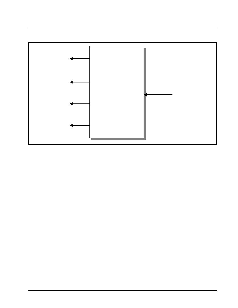
·Á
·Á
·Á
·Á
XRT7250
DS3/E3 FRAMER IC
REV. 1.1.1
309
The E3, ITU-T G.751 frame consists of 1536 bits. Of
these bytes, 1524 bits are payload bits and the re-
maining 12 bits are overhead bits. The XRT7250 has
been designed to handle and process both the pay-
load type and overhead type bits for each E3 frame.
Within the Receive Section of the XRT7250, the Re-
ceive Payload Data Output Interface block has been
designed to handle the payload bits. Likewise, the
Receive Overhead Data Output Interface block has
been designed to handle and process the overhead
bits.
The Receive Overhead Data Output Interface block
unconditionally outputs the contents of all overhead
bits. The XRT7250 does not offer the user a means
to shut off this transmission of data. However, the
Receive Overhead Output Interface block does pro-
vide the user with the appropriate output signals for
external Data Link Layer equipment to sample and
process these overhead bits, via the following two
methods.
∑ Method 1- Using the RxOHClk clock signal.
∑ Method 2 - Using the RxClk and RxOHEnable out-
put signals.
Each of these methods are described below.
5.3.4.1
Method 1 - Using the RxOHClk Clock
signal
The Receive Overhead Data Output Interface block
consists of four (4) signals. Of these four signals, the
following three signals are to be used when sampling
the E3 overhead bits via Method 1.
∑ RxOH
∑ RxOHClk
∑ RxOHFrame
Each of these signals are listed and described below
in Table 63.
Interfacing the Receive Overhead Data Output In-
terface block to the Terminal Equipment (Method
1)
Figure 145 illustrates how one should interface the
Receive Overhead Data Output Interface block to the
Terminal Equipment when using Method 1 to sample
and process the overhead bits from the inbound E3
data stream.
F
IGURE
144. A S
IMPLE
I
LLUSTRATION
OF
THE
R
ECEIVE
O
VERHEAD
O
UTPUT
I
NTERFACE
BLOCK
Receive Overhead
Output Interface
Block
Receive Overhead
Output Interface
Block
From Receive
E3 Framer Block
RxOHFrame
RxOH
RxOHClk
RxOHEnable
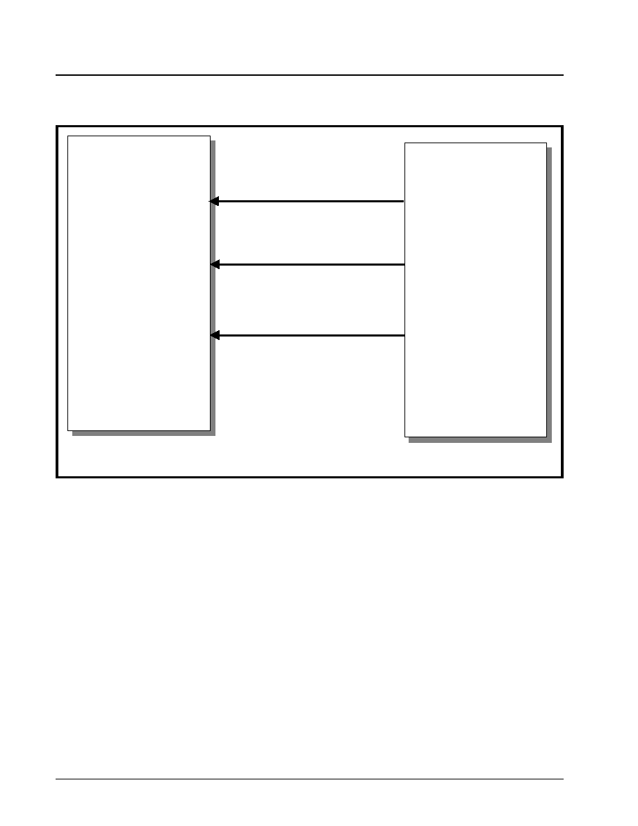
XRT7250
·Á
·Á
·Á
·Á
DS3/E3 FRAMER IC
REV. 1.1.1
310
Method 1 Operation of the Terminal Equipment
If the Terminal Equipment intends to sample any
overhead data from the inbound E3 data stream (via
the Receive Overhead Data Output Interface block)
then it is expected to do the following:
1. Sample the state of the RxOHFrame signal (e.g.,
the Rx_Start_of_Frame input signal) on the rising
edge of the RxOHClk (e.g., the
E3_OH_Clock_In) signal.
2. Keep track of the number of rising clock edges
that have occurred in the RxOHClk (e.g., the
E3_OH_Clock_In) signal, since the last time the
RxOHFrame signal was sampled "High". By
doing this, the Terminal Equipment will be able to
keep track of which overhead byte is being output
via the RxOH output pin. Based upon this infor-
mation, the Terminal Equipment will be able to
derive some meaning from these overhead bits.
F
IGURE
145. I
LLUSTRATION
OF
HOW
TO
INTERFACE
THE
T
ERMINAL
E
QUIPMENT
TO
THE
R
ECEIVE
O
VERHEAD
D
ATA
O
UTPUT
I
NTERFACE
BLOCK
(
FOR
M
ETHOD
1).
Terminal Equipment
XRT7250 E3 Framer IC
RxOHClk
E3_OH_Clock_In
RxOH
RxOHFrame
E3_OH_In
Rx_Start_of_Frame

·Á
·Á
·Á
·Á
XRT7250
DS3/E3 FRAMER IC
REV. 1.1.1
311
Table 64 relates the number of rising clock edges (in
the RxOHClk signal, since the RxOHFrame signal
was last sampled "High") to the E3 Overhead bit that
is being output via the RxOH output pin.
Figure 146 presents the typical behavior of the Re-
ceive Overhead Data Output Interface block, when
Method 1 is being used to sample the incoming E3
overhead bits.
T
ABLE
63: L
ISTING
AND
D
ESCRIPTION
OF
THE
P
IN
A
SSOCIATED
WITH
THE
R
ECEIVE
O
VERHEAD
D
ATA
O
UTPUT
I
NTERFACE
B
LOCK
(F
OR
M
ETHOD
1)
S
IGNAL
N
AME
T
YPE
D
ESCRIPTION
RxOH
Output
Receive Overhead Data Output pin:
The XRT7250 will output the overhead bits, within the incoming E3 frames, via this pin.
The Receive Overhead Data Output Interface block will output a given overhead bit, upon the
falling edge of RxOHClk. Hence, the external data link equipment should sample the data, at
this pin, upon the rising edge of RxOHClk.
N
OTE
: The XRT7250 will always output the E3 Overhead bits via this output pin. There are no
external input pins or register bit settings available that will disable this output pin.
RxOHClk
Output
Receive Overhead Data Output Interface Clock Signal:
The XRT7250 will output the Overhead bits (within the incoming E3 frames), via the RxOH out-
put pin, upon the falling edge of this clock signal.
As a consequence, the user's data link equipment should use the rising edge of this clock sig-
nal to sample the data on both the RxOH and RxOHFrame output pins.
N
OTE
: This clock signal is always active.
RxOHFrame
Output
Receive Overhead Data Output Interface - Start of Frame Indicator:
The XRT7250 will drive this output pin "High" (for one period of the RxOHClk signal) whenever
the first overhead bit within a given E3 frame is being driven onto the RxOH output pin.
T
ABLE
64: T
HE
R
ELATIONSHIP
BETWEEN
THE
N
UMBER
OF
R
ISING
C
LOCK
E
DGES
IN
R
X
OHC
LK
, (
SINCE
R
X
OHF
RAME
WAS
LAST
SAMPLED
"H
IGH
")
TO
THE
E3 O
VERHEAD
B
IT
,
THAT
IS
BEING
OUTPUT
VIA
THE
R
X
OH
OUTPUT
PIN
N
UMBER
OF
R
ISING
C
LOCK
E
DGES
IN
R
X
OHC
LK
T
HE
O
VERHEAD
B
IT
BEING
OUTPUT
BY
THE
XRT7250
0 (Clock edge is coincident with RxOHFrame being detected "High")
FAS Pattern - Bit 9
1
FAS Pattern - Bit 8
2
FAS Pattern - Bit 7
3
FAS Pattern - Bit 6
4
FAS Pattern - Bit 5
5
FAS Pattern - Bit 4
6
FAS Pattern - Bit 3
7
FAS Pattern - Bit 2
8
FAS Pattern - Bit 1
9
FAS Pattern - Bit 0
10
A Bit
11
N Bit
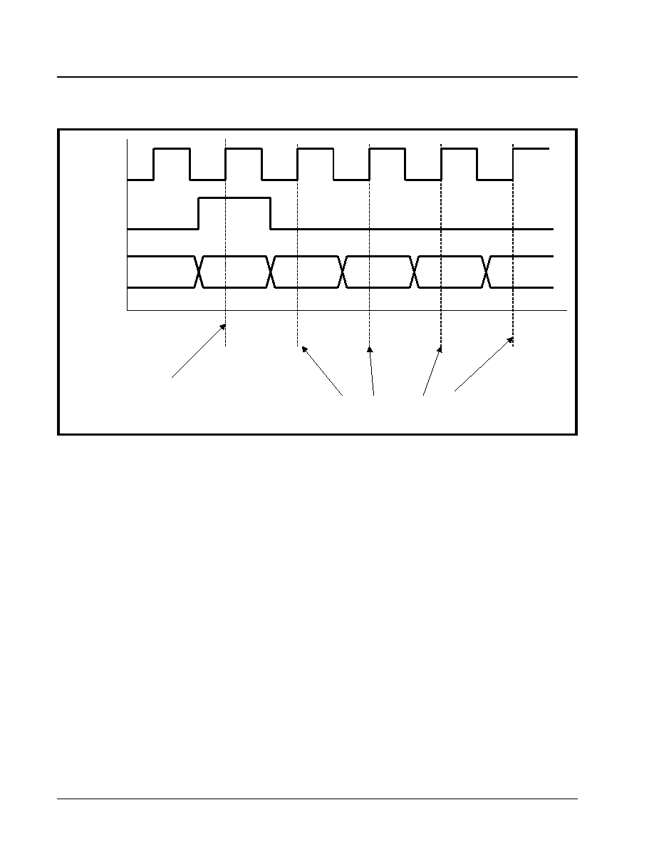
XRT7250
·Á
·Á
·Á
·Á
DS3/E3 FRAMER IC
REV. 1.1.1
312
Method 2 - Using RxOutClk and the RxOHEnable
signals
Method 1 requires that the Terminal Equipment be
able to handle an additional clock signal, RxOHClk.
However, there may be a situation in which the Termi-
nal Equipment circuitry does not have the means to
deal with this extra clock signal, in order to use the
Receive Overhead Data Output Interface. Method 2
involves the use of the following signals.
∑ RxOH
∑ RxOutClk
∑ RxOHEnable
∑ RxOHFrame
Each of these signals are listed and described below
in Table 65.
F
IGURE
146. I
LLUSTRATION
OF
THE
SIGNALS
THAT
ARE
OUTPUT
VIA
THE
R
ECEIVE
O
VERHEAD
O
UTPUT
I
NTERFACE
(
FOR
M
ETHOD
1).
RxOHClk
RxOHFrame
RxOH
FAS, Bit 9 FAS, Bit 8 FAS, Bit 7 FAS, Bit 6 FAS, Bit 5
Terminal Equipment should sample
the "RxOHFrame" and "RxOH" signals
here.
Recommended Sampling Edges

·Á
·Á
·Á
·Á
XRT7250
DS3/E3 FRAMER IC
REV. 1.1.1
313
Interfacing the Receive Overhead Data Output In-
terface block to the Terminal Equipment (Method
2)
Figure 147 illustrates how one should interface the
Receive Overhead Data Output Interface block to the
Terminal Equipment, when using Method 2 to sample
and process the overhead bits from the inbound E3
data stream.
T
ABLE
65: L
ISTING
AND
D
ESCRIPTION
OF
THE
P
IN
A
SSOCIATED
WITH
THE
R
ECEIVE
O
VERHEAD
D
ATA
O
UTPUT
I
NTERFACE
B
LOCK
(M
ETHOD
2)
S
IGNAL
N
AME
T
YPE
D
ESCRIPTION
RxOH
Output
Receive Overhead Data Output pin:
The XRT7250 will output the overhead bits, within the incoming E3 frames, via this pin.
The Receive Overhead Output Interface will pulse the RxOHEnable output pin (for one RxOut-
Clk period) at approximately the middle of the RxOH bit period. The user is advised to design
the Terminal Equipment to latch the contents of the RxOH output pin, whenever the RxOHEn-
able output pin is sampled "High" on the falling edge of RxOutClk.
RxOHEnable
Output
Receive Overhead Data Output Enable - Output pin:
The XRT7250 will assert this output signal for one RxOutClk period when it is safe for the Ter-
minal Equipment to sample the data on the RxOH output pin.
RxOHFrame
Output
Receive Overhead Data Output Interface - Start of Frame Indicator:
The XRT7250 will drive this output pin "High" (for one period of the RxOH signal), whenever the
first overhead bit, within a given E3 frame is being driven onto the RxOH output pin.
RxOutClk
Output
Receive Section Output Clock Signal:
This clock signal is derived from the RxLineClk signal (from the LIU) for loop-timing applica-
tions, and the TxInClk signal (from a local oscillator) for local-timing applications. For E3 appli-
cations, this clock signal will operate at 34.368MHz.
The user is advised to design the Terminal Equipment to latch the contents of the RxOH pin,
anytime the RxOHEnable output signal is sampled "High" on the falling edge of this clock sig-
nal.
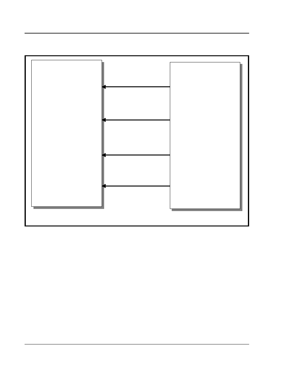
XRT7250
·Á
·Á
·Á
·Á
DS3/E3 FRAMER IC
REV. 1.1.1
314
Method 2 Operation of the Terminal Equipment
If the Terminal Equipment intends to sample any
overhead data from the inbound E3 data stream (via
the Receive Overhead Data Output Interface), then it
is expected to do the following.
1. Sample the state of the RxOHFrame signal (e.g.,
the Rx_Start_of_Frame input) on the falling edge
of the RxOutClk clock signal, whenever the RxO-
HEnable output signal is also sampled "High".
2. Keep track of the number of times that the RxO-
HEnable signal has been sampled "High" since
the last time the RxOHFrame was also sampled
"High". By doing this, the Terminal Equipment will
be able to keep track of which overhead bit is
being output via the RxOH output pin. Based
upon this information, the Terminal Equipment
will be able to derive some meaning from these
overhead bits.
3. Table 66 relates the number of RxOHEnable out-
put pulses (that have occurred since both the
RxOHFrame and the RxOHEnable pins were
both sampled "High") to the E3 overhead bit that
is being output via the RxOH output pin.
F
IGURE
147. I
LLUSTRATION
OF
HOW
TO
INTERFACE
THE
T
ERMINAL
E
QUIPMENT
TO
THE
R
ECEIVE
O
VERHEAD
D
ATA
O
UTPUT
I
NTERFACE
BLOCK
(
FOR
M
ETHOD
2).
RxOH
RxOHEnable
RxOutClk
RxOHFrame
E3_OH_In
E3_OH_Enable_In
E3_Clk_In
Rx_Start_of_Frame
Terminal Equipment
XRT7250 E3 Framer IC
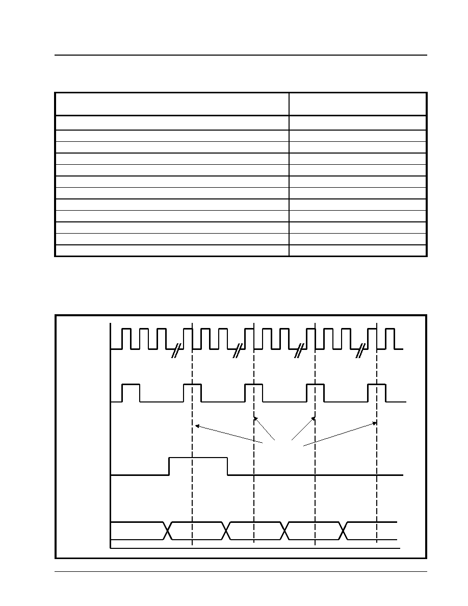
·Á
·Á
·Á
·Á
XRT7250
DS3/E3 FRAMER IC
REV. 1.1.1
315
Figure 148 presents the typical behavior of the Re-
ceive Overhead Data Output Interface block, when
Method 2 is being used to sample the incoming E3
overhead bits.
T
ABLE
66: T
HE
R
ELATIONSHIP
BETWEEN
THE
N
UMBER
OF
R
X
OHE
NABLE
OUTPUT
PULSES
(
SINCE
R
X
OHF
RAME
WAS
LAST
SAMPLED
"H
IGH
")
TO
THE
E3 O
VERHEAD
B
IT
,
THAT
IS
BEING
OUTPUT
VIA
THE
R
X
OH
OUTPUT
PIN
N
UMBER
OF
R
X
OHE
NABLE
O
UTPUT
P
ULSES
T
HE
O
VERHEAD
B
IT
BEING
OUTPUT
BY
THE
XRT7250
0 (Clock edge is coincident with RxOHFrame being detected "High")
FAS Pattern - Bit 9
1
FAS Pattern - Bit 8
2
FAS Pattern - Bit 7
3
FAS Pattern - Bit 6
4
FAS Pattern - Bit 5
5
FAS Pattern - Bit 4
6
FAS Pattern - Bit 3
7
FAS Pattern - Bit 2
8
FAS Pattern - Bit 1
9
FAS Pattern - Bit 0
10
A Bit
11
N Bit
F
IGURE
148. I
LLUSTRATION
OF
THE
SIGNALS
THAT
ARE
OUTPUT
VIA
THE
R
ECEIVE
O
VERHEAD
D
ATA
O
UTPUT
I
NTER
-
FACE
BLOCK
(
FOR
M
ETHOD
2).
RxOutClk
RxOHEnable
RxOHFrame
RxOH
BIP - 4, Bit 0 FAS, Bit 9 FAS, Bit 8 FAS, Bit 7 FAS, Bit 6
Recommended
Sampling
Edges
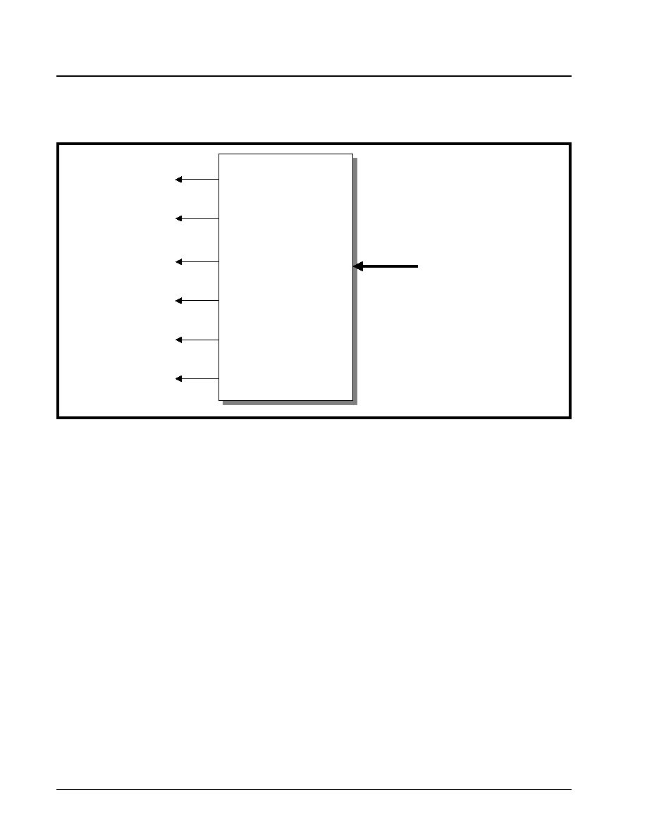
XRT7250
·Á
·Á
·Á
·Á
DS3/E3 FRAMER IC
REV. 1.1.1
316
5.3.5
The Receive Payload Data Output Inter-
face
Figure 149 presents a simple illustration of the Re-
ceive Payload Data Output Interface block.
Each of the output pins of the Receive Payload Data
Output Interface block are listed in Table 67 and de-
scribed below. The exact role that each of these out-
put pins assume, for a variety of operating scenarios
are described throughout this section.
F
IGURE
149. A S
IMPLE
ILLUSTRATION
OF
THE
R
ECEIVE
P
AYLOAD
D
ATA
O
UTPUT
I
NTERFACE
BLOCK
Receive Payload
Data Output
Interface
Receive Payload
Data Output
Interface
RxOHInd
RxSer
RxNib[3:0]
RxClk
RxOutClk
RxFrame
From Receive E3
Framer Block

·Á
·Á
·Á
·Á
XRT7250
DS3/E3 FRAMER IC
REV. 1.1.1
317
T
ABLE
67: L
ISTING
AND
D
ESCRIPTION
OF
THE
PIN
ASSOCIATED
WITH
THE
R
ECEIVE
P
AYLOAD
D
ATA
O
UTPUT
I
NTERFACE
BLOCK
S
IGNAL
N
AME
T
YPE
D
ESCRIPTION
RxSer
Output
Receive Serial Payload Data Output pin:
If the user opts to operate the XRT7250 in the serial mode, then the chip will output the pay-
load data, of the incoming E3 frames, via this pin. The XRT7250 will output this data upon the
rising edge of RxClk.
The user is advised to design the Terminal Equipment such that it will sample this data on the
falling edge of RxClk.
This signal is only active if the NibInt input pin is pulled "Low".
RxNib[3:0]
Output
Receive Nibble-Parallel Payload Data Output pins:
If the user opts to operate the XRT7250 in the nibble-parallel mode, then the chip will output
the payload data, of the incoming E3 frames, via these pins. The XRT7250 will output data via
these pins, upon the falling edge of the RxClk output pin.
The user is advised to design the Terminal Equipment such that it will sample this data upon
the rising edge of RxClk.
N
OTE
: These pins are only active if the NibInt input pin is pulled "High".
RxClk
Output
Receive Payload Data Output Clock pin:
The exact behavior of this signal depends upon whether the XRT7250 is operating in the Serial
or in the Nibble-Parallel-Mode.
Serial Mode Operation
In the serial mode, this signal is a 34.368MHz clock output signal. The Receive Payload Data
Output Interface will update the data via the RxSer output pin, upon the rising edge of this
clock signal.
The user is advised to design (or configure) the Terminal Equipment to sample the data on the
RxSer pin, upon the falling edge of this clock signal.
Nibble-Parallel Mode Operation
In this Nibble-Parallel Mode, the XRT7250 will derive this clock signal, from the RxLineClk sig-
nal. The XRT7250 will pulse this clock 1060 times for each inbound E3 frame. The Receive
Payload Data Output Interface will update the data, on the RxNib[3:0] output pins upon the fall-
ing edge of this clock signal.
The user is advised to design (or configure) the Terminal Equipment to sample the data on the
RxNib[3:0] output pins, upon the rising edge of this clock signal
RxOHInd
Output
Receive Overhead Bit Indicator Output:
This output pin will pulse "High" whenever the Receive Payload Data Output Interface outputs
an overhead bit via the RxSer output pin. The purpose of this output pin is to alert the Terminal
Equipment that the current bit, (which is now residing on the RxSer output pin), is an overhead
bit and should not be processed by the Terminal Equipment.
The XRT7250 will update this signal, upon the rising edge of RxOHInd.
The user is advised to design (or configure) the Terminal Equipment to sample this signal
(along with the data on the RxSer output pin) on the falling edge of the RxClk signal.
N
OTE
: For E3 applications, this output pin is only active if the XRT7250 is operating in the
Serial Mode. This output pin will be "Low" if the device is operating in the Nibble-Parallel
Mode.
RxFrame
Output
Receive Start of Frame Output Indicator:
The exact behavior of this pin, depends upon whether the XRT7250 has been configured to
operate in the Serial Mode or the Nibble-Parallel Mode.
Serial Mode Operation:
The Receive Section of the XRT7250 will pulse this output pin "High" (for one bit period) when
the Receive Payload Data Output Interface block is driving the very first bit (or Nibble) of a
given E3 frame, onto the RxSer output pin.
Nibble-Parallel Mode Operation:
The Receive Section of the XRT7250 will pulse this output pin "High" for one nibble period,
when the Receive Payload Data Output Interface is driving the very first nibble of a given E3
frame, onto the RxNib[3:0] output pins.
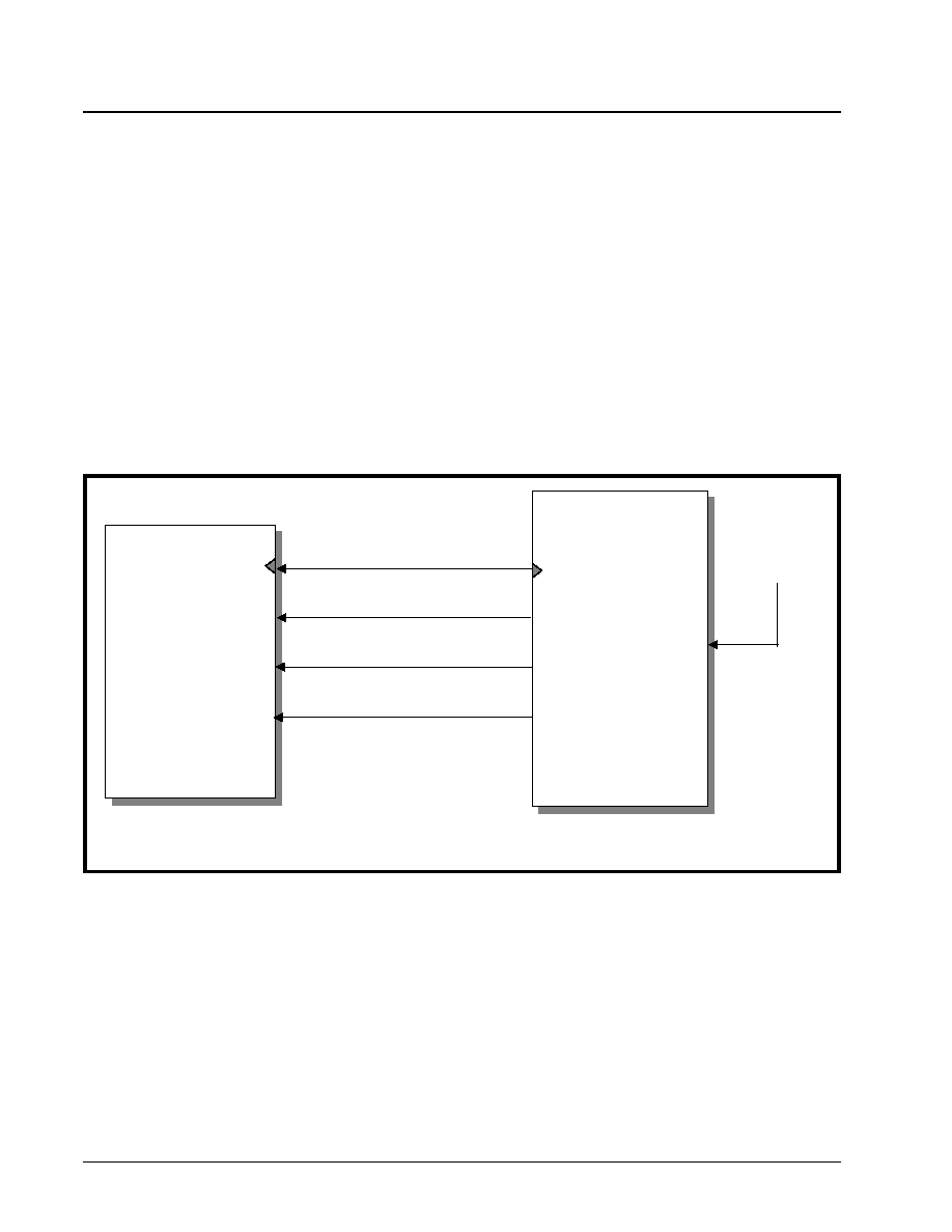
XRT7250
·Á
·Á
·Á
·Á
DS3/E3 FRAMER IC
REV. 1.1.1
318
Operation of the Receive Payload Data Output In-
terface block
The Receive Payload Data Output Interface permits
the user to read out the payload data of inbound E3
frames, via either of the following modes.
∑ Serial Mode
∑ Nibble-Parallel Mode
Each of these modes are described in detail, below.
5.3.5.1
Serial Mode Operation Behavior of the
XRT7250
If the XRT7250 has been configured to operate in this
mode, then the XRT7250 will behave as follows.
Payload Data Output
The XRT7250 will output the payload data, of the in-
coming E3 frames via the RxSer output pin, upon the
rising edge of RxClk.
Delineation of inbound E3 Frames
The XRT7250 will pulse the RxFrame output pin
"High" for one bit-period coincident with it driving the
first bit within a given E3 frame, via the RxSer output
pin.
Interfacing the XRT7250 to the Receive Terminal
Equipment
Figure 150 presents a simple illustration as how the
user should interface the XRT7250 to that terminal
equipment which processes Receive Direction pay-
load data.
Required Operation of the Terminal Equipment
The XRT7250 will update the data on the RxSer out-
put pin, upon the rising edge of RxClk. Hence, the
Terminal Equipment should sample the data on the
RxSer output pin (or the E3_Data_In pin at the Termi-
nal Equipment) upon the rising edge of RxClk. As the
Terminal Equipment samples RxSer with each rising
edge of RxClk it should also be sampling the follow-
ing signals.
∑ RxFrame
∑ RxOHInd
The Need for sampling RxFrame
The XRT7250 will pulse the RxFrame output pin
"High" coincident with it driving the very first bit of a
given E3 frame onto the RxSer output pin. If knowl-
edge of the E3 Frame Boundaries is important for the
operation of the Terminal Equipment, then this is a
very important signal for it to sample.
The Need for sampling RxOHInd
The XRT7250 will indicate that it is currently driving
an overhead bit onto the RxSer output pin, by pulsing
the RxOHInd output pin "High". If the Terminal Equip-
ment samples this signal "High", then it should know
that the bit, that it is currently sampling via the RxSer
pin is an overhead bit and should not be processed.
F
IGURE
150. I
LLUSTRATION
OF
THE
T
ERMINAL
E
QUIPMENT
BEING
INTERFACED
TO
THE
R
ECEIVE
P
AYLOAD
D
ATA
I
NPUT
I
NTERFACE
B
LOCK
OF
THE
XRT7250 F
RAMER
IC (S
ERIAL
M
ODE
O
PERATION
)
Terminal Equipment
(Receive Payload Section)
XRT7250 E3 Framer
E3_Data_In
Rx_E3_Clock_In
Rx_Start_of_Frame
RxClk
RxFrame
RxOHInd
34.368 MHz Clock Signal
RxSer
Rx_E3_OH_Ind
RxLineClk
34.368 MHz
Clock Source
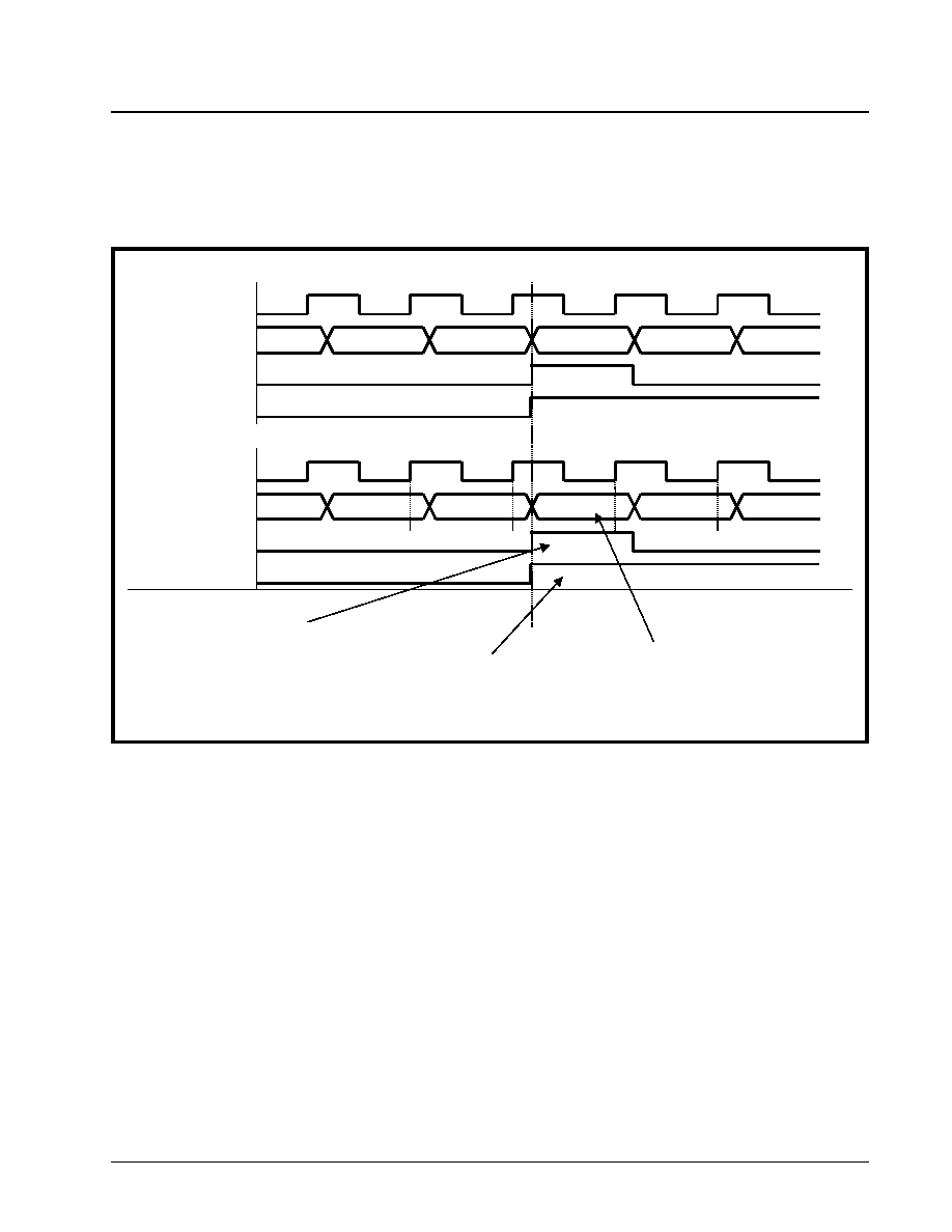
·Á
·Á
·Á
·Á
XRT7250
DS3/E3 FRAMER IC
REV. 1.1.1
319
The Behavior of the Signals between the Receive
Payload Data Output Interface block and the Ter-
minal Equipment
The behavior of the signals between the XRT7250
and the Terminal Equipment for E3 Serial Mode Op-
eration is illustrated in Figure 151.
5.3.5.2
Nibble-Parallel Mode Operation Behav-
ior of the XRT7250
If the XRT7250 has been configured to operate in the
Nibble-Parallel Mode, then the XRT7250 will behave
as follows.
Payload Data Output
The XRT7250 will output the payload data of the in-
coming E3 frames, via the RxNib[3:0] output pins, up-
on the rising edge of RxClk.
N
OTES
:
1. In this case, RxClk will function as the Nibble Clock
signal between the XRT7250 the Terminal Equip-
ment. The XRT7250 will pulse the RxClk output
signal "High" 1060 times, for each inbound E3
frame.
2. Unlike Serial Mode operation, the duty cycle of
RxClk, in Nibble-Parallel Mode operation is approx-
imately 25%.
Delineation of Inbound E3 Frames
The XRT7250 will pulse the RxFrame output pin
"High" for one nibble-period coincident with it driving
the very first nibble, within a given inbound E3 frame,
via the RxNib[3:0] output pins.
Interfacing the XRT7250 the Terminal Equipment.
Figure 152 presents a simple illustration as how the
user should interface the XRT7250 to that terminal
equipment which processes Receive Direction pay-
load data.
F
IGURE
151. A
N
I
LLUSTRATION
OF
THE
BEHAVIOR
OF
THE
SIGNALS
BETWEEN
THE
R
ECEIVE
P
AYLOAD
D
ATA
O
UT
-
PUT
I
NTERFACE
BLOCK
OF
THE
XRT7250
AND
THE
T
ERMINAL
E
QUIPMENT
Terminal Equipment Signals
E3_Clock_In
E3_Data_Out
Rx_Start_of_Frame
E3_Overhead_Ind
XRT7250 Receive Payload Data I/F Signals
RxClk
RxSer
RxFrame
RxOH_Ind
Payload[1522]
Payload[1523]
FAS , Bit 9
FAS, Bit 8
Payload[1522]
Payload[1523]
FAS, Bit 9
FAS, Bit 8
Note: FAS pattern will not be processed by the
Transmit Payload Data Input Interface.
E3 Frame Number N
E3 Frame Number N + 1
Note: RxFrame pulses high to denote
E3 Frame Boundary.
Note: RxOH_Ind pulses high for 12
bit-periods in order to denote
Overhead Data (e.g., the FAS pattern,
the A and N bits).
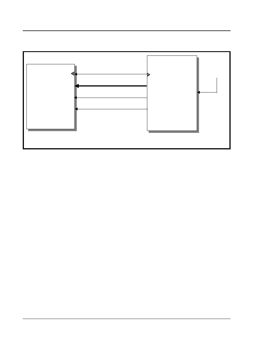
XRT7250
·Á
·Á
·Á
·Á
DS3/E3 FRAMER IC
REV. 1.1.1
320
Required Operation of the Terminal Equipment
The XRT7250 will update the data on the RxNib[3:0]
line, upon the rising edge of RxClk. Hence, the Ter-
minal Equipment should sample the data on the Rx-
Nib[3:0] output pins (or the E3_Data_In[3:0] input
pins at the Terminal Equipment) upon the rising edge
of RxClk. As the Terminal Equipment samples RxSer
with each rising edge of RxClk it should also be sam-
pling the RxFrame signal.
The Need for Sampling RxFrame
The XRT7250 will pulse the RxFrame output pin
"High" coincident with it driving the very first nibble of
a given E3 frame, onto the RxNib[3:0] output pins. If
knowledge of the E3 Frame Boundaries is important
for the operation of the Terminal Equipment, then this
is a very important signal for it to sample.
The Behavior of the Signals between the Receive
Payload Data Output Interface block and the Ter-
minal Equipment
The behavior of the signals between the XRT7250
and the Terminal Equipment for E3 Nibble-Mode op-
eration is illustrated in Figure 153.
F
IGURE
152. I
LLUSTRATION
OF
THE
XRT7250 DS3/E3 F
RAMER
IC
BEING
INTERFACED
TO
THE
R
ECEIVE
S
ECTION
OF
THE
T
ERMINAL
E
QUIPMENT
(N
IBBLE
-P
ARALLEL
M
ODE
O
PERATION
)
Terminal Equipment
(Receive Payload Section)
XRT7250 E3 Framer
E3_Data_In[3:0]
Rx_E3_Clock_In
Rx_Start_of_Frame
RxClk
RxFrame
8.592 MHz Clock Signal
RxNib[3:0]
RxLineClk
34.368 MHz
Clock Source
RxOH_Ind
Rx_E3_OH_Ind
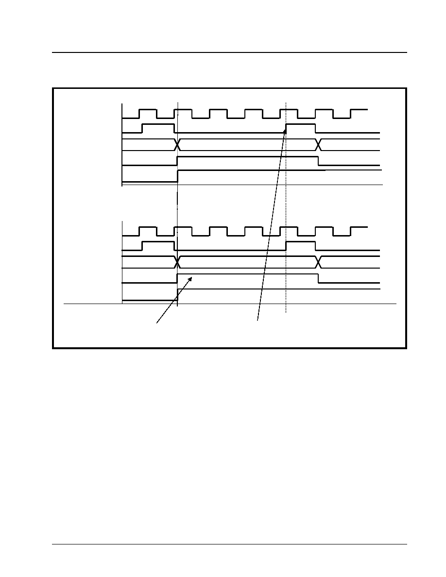
·Á
·Á
·Á
·Á
XRT7250
DS3/E3 FRAMER IC
REV. 1.1.1
321
5.3.6
Receive Section Interrupt Processing
The Receive Section of the XRT7250 can generate
an interrupt to the MIcrocontroller/Microprocessor for
the following reasons.
∑ Change in Receive LOS Condition
∑ Change in Receive OOF Condition
∑ Change in Receive LOF Condition
∑ Change in Receive AIS Condition
∑ Change in Receive FERF Condition
∑ Change of Framing Alignment
∑ Detection of FEBE (Far-End Block Error) Event
∑ Detection of BIP-4 Error
∑ Detection of Framing Error
∑ Reception of a new LAPD Message
5.3.6.1
Enabling Receive Section Interrupts
As mentioned in Section 1.6, the Interrupt Structure
within the XRT7250 contains two hierarchical levels.
∑ Block Level
∑ Source Level
The Block Level
The Enable state of the Block level for the Receive
Section Interrupts dictates whether or not interrupts
(if enabled at the source level), are actually enabled.
The user can enable or disable these Receive Sec-
tion interrupts, at the Block Level by writing the appro-
priate data into Bit 7 (Rx DS3/E3 Interrupt Enable)
within the Block Interrupt Enable register (Address =
0x04), as illustrated below.
F
IGURE
153. I
LLUSTRATION
OF
THE
SIGNALS
THAT
ARE
OUTPUT
VIA
THE
R
ECEIVE
P
AYLOAD
D
ATA
O
UTPUT
I
NTER
-
FACE
BLOCK
(
FOR
N
IBBLE
-P
ARALLEL
M
ODE
O
PERATION
).
XRT7250 Receive Payload Data I/F Signals
E3 Frame Number N
E3 Frame Number N + 1
Note: RxFrame pulses high to denote
E3 Frame Boundary.
Terminal Equipment Signals
RxOutClk
Rx_Start_of_Frame
Rx_E3_Clock_In
E3_Data_In[3:0]
Overhead Nibble [0]
Overhead Nibble [1]
RxOutClk
RxFrame
RxClk
RxNib[3:0]
Overhead Nibble [0]
Overhead Nibble [1]
Recommended Sampling Edge of Terminal
Equipment
Rx_E3_OH_Ind
RxOH_Ind

XRT7250
·Á
·Á
·Á
·Á
DS3/E3 FRAMER IC
REV. 1.1.1
322
Setting this bit-field to "1" enables the Receive Sec-
tion at the Block Level) for interrupt generation. Con-
versely, setting this bit-field to "0" disables the Re-
ceive Section for interrupt generation.
5.3.6.2
Enabling/Disabling and Servicing Inter-
rupts
As mentioned previously, the Receive Section of the
XRT7250 Framer IC contains numerous interrupts.
The Enabling/Disabling and Servicing of each of
these interrupts is described below.
5.3.6.2.1
The Change in Receive LOS Condi-
tion Interrupt
If the Change in Receive LOS Condition Interrupt is
enabled, then the XRT7250 Framer IC will generate
an interrupt in response to either of the following con-
ditions.
1. When the XRT7250 Framer IC declares an LOS
(Loss of Signal) Condition, and
2. When the XRT7250 Framer IC clears the LOS
condition.
Conditions causing the XRT7250 Framer IC to de-
clare an LOS Condition.
∑ If the XRT7300 LIU IC declares an LOS condition,
and drives the RLOS input pin (of the XRT7250
Framer IC) "High".
∑ If the XRT7250 Framer IC detects 32 consecutive
"0", via the RxPOS and RxNEG input pins.
Conditions causing the XRT7250 Framer IC to
clear the LOS Condition.
∑ If the XRT7300 LIU IC clears the LOS condition and
drives the RLOS input pin (of the XRT7250 Framer
IC) "Low".
∑ If the XRT7250 Framer IC detects a string of 32
consecutive bits (via the RxPOS and RxNEG input
pins) that does NOT contain a string of 4 consecu-
tive "0's".
Enabling and Disabling the Change in Receive
LOS Condition Interrupt
The user can enable or disable the Change in Re-
ceive LOS Condition Interrupt, by writing the appro-
priate value into Bit 1 (LOS Interrupt Enable), within
the RxE3 Interrupt Enable Register - 1, as indicated
below.
Setting this bit-field to "1" enables this interrupt. Con-
versely, setting this bit-field to "0" disables this inter-
rupt.
Servicing the Change in Receive LOS Condition
Interrupt
Whenever the XRT7250 Framer IC detects this inter-
rupt, it will do all of the following.
∑ It will assert the Interrupt Request output pin (INT),
by driving it "Low".
∑ It will set Bit 1 (LOS Interrupt Status), within the Rx
E3 Interrupt Status Register - 1 to "1", as indicated
below.
BLOCK INTERRUPT ENABLE REGISTER (ADDRESS = 0X04)
B
IT
7
B
IT
6
B
IT
5
B
IT
4
B
IT
3
B
IT
2
B
IT
1
B
IT
0
RxDS3/E3
Interrupt
Enable
Not Used
TxDS3/E3
Interrupt
Enable
One-Second
Interrupt
Enable
R/W
RO
RO
RO
RO
RO
R/W
R/W
X
0
0
0
0
0
0
0
RXE3 INTERRUPT ENABLE REGISTER - 1 (ADDRESS = 0X12)
B
IT
7
B
IT
6
B
IT
5
B
IT
4
B
IT
3
B
IT
2
B
IT
1
B
IT
0
Not Used
COFA
Interrupt
Enable
OOF
Interrupt
Enable
LOF
Interrupt
Enable
LOS
Interrupt
Enable
AIS
Interrupt
Enable
RO
RO
RO
R/W
R/W
R/W
R/W
R/W
0
0
0
0
0
0
X
0

·Á
·Á
·Á
·Á
XRT7250
DS3/E3 FRAMER IC
REV. 1.1.1
323
Whenever the user's system encounters the Change
in Receive LOS Condition Interrupt, then it should do
the following.
1. It should determine the current state of the LOS
condition. Recall, that this interrupt can be gen-
erated, whenever the XRT7250 Framer IC
declares or clears the LOS defect. Hence, the
user can determine the current state of the LOS
defect by reading the state of Bit 4 (RxLOS)
within the Rx E3 Configuration and Status Regis-
ter - 2, as illustrated below.
If the LOS state is TRUE
1. It should transmit a FERF (Far-End-Receive Fail-
ure) indicator to the Remote Terminal Equipment.
Please see Section 4.2.4.2.1.3 on how to config-
ure the XRT7250 to transmit a FERF indicator to
the Remote Terminal Equipment.
If the LOS state is FALSE
1. It should cease transmitting the FERF indication
to the Remote Terminal Equipment. Please see
Section 4.2.4.2.1.3 on how to control the state of
the "A" bit, which is transmitted on each outbound
E3 frame.
5.3.6.2.2
The Change in Receive OOF Condi-
tion Interrupt
If the Change in Receive OOF Condition Interrupt is
enabled, then the XRT7250 Framer IC will generate
an interrupt in response to either of the following con-
ditions.
1. When the XRT7250 Framer IC declares an OOF
(Out of Frame) Condition, and
2. When the XRT7250 Framer IC clears the OOF
condition.
Conditions causing the XRT7250 Framer IC to de-
clare an OOF Condition.
∑ If the Receive E3 Framer block (within the XRT7250
Framer IC) detects Framing bit errors, within four
consecutive incoming E3 frames.
Conditions causing the XRT7250 Framer IC to
clear the OOF Condition.
∑ If the Receive E3 Framer block (within the XRT7250
Framer IC) transitions from the FAS Pattern Verifi-
cation state to the In-Frame state (see Figure 115).
∑ If the Receive E3 Framer block transitions from the
OOF Condition state to the In-Frame state (see Fig-
ure 115).
Enabling and Disabling the Change in Receive
OOF Condition Interrupt
The user can enable or disable the Change in Re-
ceive OOF Condition Interrupt, by writing the appro-
priate value into Bit 3 (OOF Interrupt Enable), within
RXE3 INTERRUPT STATUS REGISTER - 1 (ADDRESS = 0X14)
B
IT
7
B
IT
6
B
IT
5
B
IT
4
B
IT
3
B
IT
2
B
IT
1
B
IT
0
Not Used
COFA
Interrupt Status
OOF
Interrupt Status
LOF
Interrupt Status
LOS
Interrupt Status
AIS
Interrupt Status
RO
RO
RO
RUR
RUR
RUR
RUR
RUR
0
0
0
0
0
0
1
0
RXE3 CONFIGURATION & STATUS REGISTER - 2 (ADDRESS = 0X11)
B
IT
7
B
IT
6
B
IT
5
B
IT
4
B
IT
3
B
IT
2
B
IT
1
B
IT
0
RxLOF
Algo
RxLOF
RxOOF
RxLOS
RxAIS
Not Used
RxFERF
R/W
RO
RO
RO
RO
RO
RO
RO
0
1
1
0
0
1
1
1
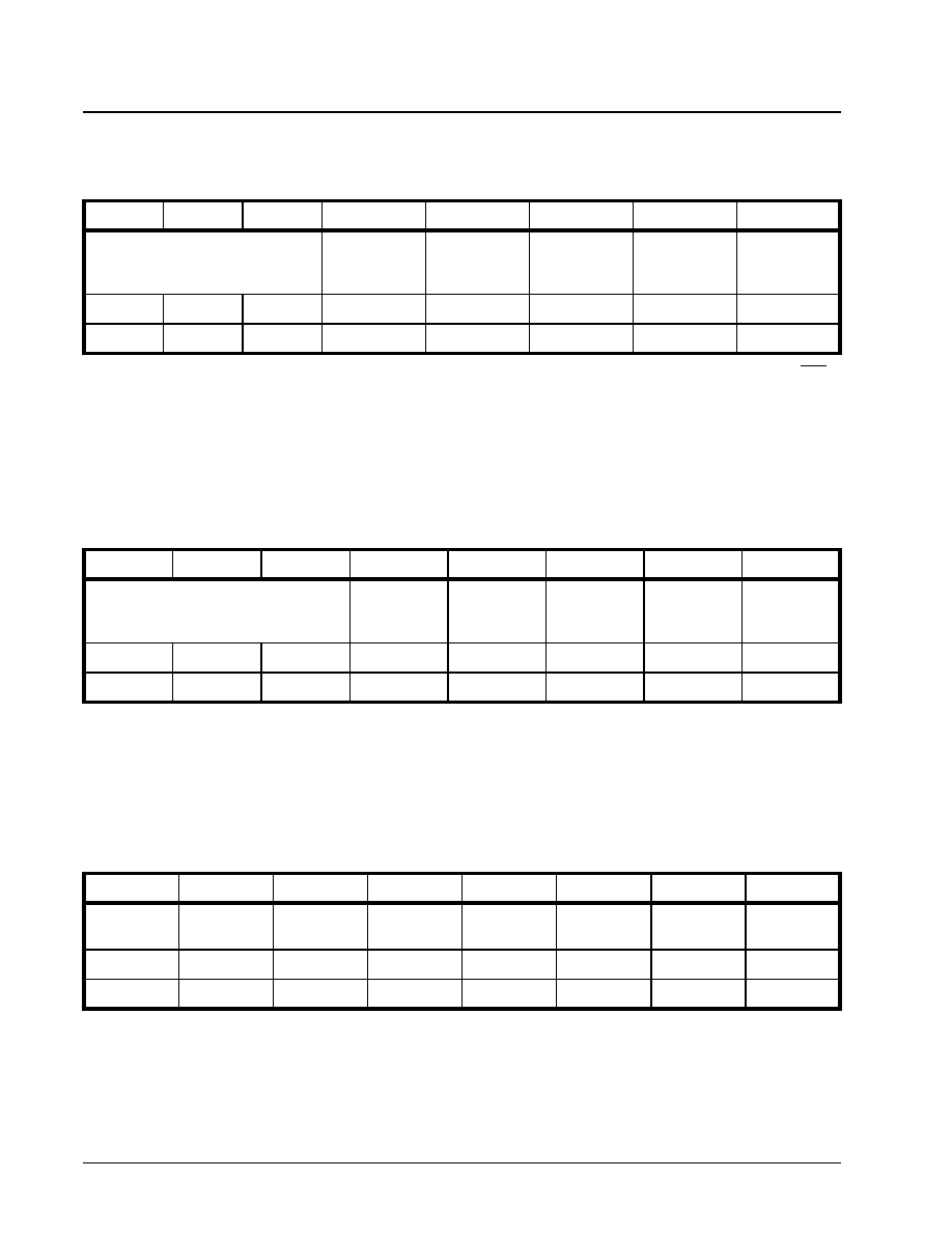
XRT7250
·Á
·Á
·Á
·Á
DS3/E3 FRAMER IC
REV. 1.1.1
324
the RxE3 Interrupt Enable Register - 1, as indicated
below.
Setting this bit-field to "1" enables this interrupt. Con-
versely, setting this bit-field to "0" disables this inter-
rupt.
Servicing the Change in Receive OOF Condition
Interrupt
Whenever the XRT7250 Framer IC detects this inter-
rupt, it will do all of the following.
∑ It will assert the Interrupt Request output pin (INT),
by driving it "Low".
∑ It will set Bit 3 (OOF Interrupt Status), within the Rx
E3 Interrupt Status Register - 1 to "1", as indicated
below.
Whenever the user's system encounters the Change
in Receive OOF Condition Interrupt, then it should do
the following.
1. It should determine the current state of the OOF
condition. Recall, that this interrupt can be gen-
erated, whenever the XRT7250 Framer IC
declares or clears the OOF defect. Hence, the
user can determine the current state of the LOS
defect by reading the state of Bit 5 (RxOOF)
within the Rx E3 Configuration and Status Regis-
ter - 2, as illustrated below.
If the OOF state is TRUE
1. It should transmit a FERF (Far-End-Receive Fail-
ure) indicator to the Remote Terminal Equipment.
Please see Section 4.2.4.2.1.3 on how to config-
ure the XRT7250 to transmit the FERF indicator
to the Remote Terminal Equipment.
If the OOF state is FALSE
1. It should cease transmitting the FERF indication
to the Remote Terminal Equipment. Please see
Section 4.2.4.2.1.3 on how to control the state of
the "A" bit, which is transmitted via each out-
bound E3 frame.
RXE3 INTERRUPT ENABLE REGISTER - 1 (ADDRESS = 0X12)
B
IT
7
B
IT
6
B
IT
5
B
IT
4
B
IT
3
B
IT
2
B
IT
1
B
IT
0
Not Used
COFA
Interrupt
Enable
OOF
Interrupt
Enable
LOF
Interrupt
Enable
LOS
Interrupt
Enable
AIS
Interrupt
Enable
RO
RO
RO
R/W
R/W
R/W
R/W
R/W
0
0
0
0
X
0
X
0
RXE3 INTERRUPT STATUS REGISTER - 1 (ADDRESS = 0X14)
B
IT
7
B
IT
6
B
IT
5
B
IT
4
B
IT
3
B
IT
2
B
IT
1
B
IT
0
Not Used
COFA
Interrupt
Status
OOF
Interrupt
Status
LOF
Interrupt
Status
LOS
Interrupt
Status
AIS
Interrupt
Status
RO
RO
RO
RUR
RUR
RUR
RUR
RUR
0
0
0
0
1
0
0
0
RXE3 CONFIGURATION & STATUS REGISTER 2 (ADDRESS = 0X11)
B
IT
7
B
IT
6
B
IT
5
B
IT
4
B
IT
3
B
IT
2
B
IT
1
B
IT
0
RxLOF Algo
RxLOF
RxOOF
RxLOS
RxAIS
RxPld Unstab
Rx
TMark
RxFERF
R/W
RO
RO
RO
RO
RO
RO
RO
X
X
X
X
X
X
X
X

·Á
·Á
·Á
·Á
XRT7250
DS3/E3 FRAMER IC
REV. 1.1.1
325
5.3.6.2.3
The Change in Receive LOF Condi-
tion Interrupt
If the Change in Receive LOF Condition Interrupt is
enabled, then the XRT7250 Framer IC will generate
an interrupt in response to either of the following con-
ditions.
1. When the XRT7250 Framer IC declares an LOF
(Out of Frame) Condition, and
2. When the XRT7250 Framer IC clears the LOF
condition.
Conditions causing the XRT7250 Framer IC to de-
clare an LOF Condition.
∑ If the Receive E3 Framer block (within the XRT7250
Framer IC) detects Framing Bit errors, within four
consecutive incoming E3 frames, and is not capa-
ble of transition back into the In-Frame state within
a 1ms or 3ms period.
Conditions causing the XRT7250 Framer IC to
clear the LOF Condition.
∑ If the Receive E3 Framer block transitions from the
OOF Condition state to the LOF Condition state
(see Figure 115).
∑ If the Receive E3 Framer block transitions back into
the In-Frame state.
Enabling and Disabling the Change in Receive
LOF Condition Interrupt
The user can enable or disable the Change in Re-
ceive LOF Condition Interrupt, by writing the appropri-
ate value into Bit 3 (LOF Interrupt Enable), within the
RxE3 Interrupt Enable Register - 1, as indicated be-
low.
Setting this bit-field to "1" enables this interrupt. Con-
versely, setting this bit-field to "0" disables this inter-
rupt.
Servicing the Change in Receive LOF Condition
Interrupt
Whenever the XRT7250 Framer IC detects this inter-
rupt, it will do all of the following.
∑ It will assert the Interrupt Request output pin (INT),
by driving it "Low".
∑ It will set Bit 6 (LOF Interrupt Status), within the Rx
E3 Interrupt Status Register - 1 to "1", as indicated
below.
5.3.6.2.4
The Change in Receive AIS Condition
Interrupt
If the Change in Receive AIS Condition Interrupt is
enabled, then the XRT7250 Framer IC will generate
an interrupt in response to either of the following con-
ditions.
1. When the XRT7250 Framer IC declares an AIS
(Loss of Signal) Condition, and
2. When the XRT7250 Framer IC clears the AIS
condition.
Conditions causing the XRT7250 Framer IC to de-
clare an AIS Condition.
∑ If the XRT7250 Framer IC detects 7 or less "0"
within 2 consecutive E3 frames.
Conditions causing the XRT7250 Framer IC to
clear the AIS Condition.
RXE3 INTERRUPT ENABLE REGISTER - 1 (ADDRESS = 0X12)
B
IT
7
B
IT
6
B
IT
5
B
IT
4
B
IT
3
B
IT
2
B
IT
1
B
IT
0
Not Used
COFA
Interrupt
Enable
OOF
Interrupt
Enable
LOF
Interrupt
Enable
LOS
Interrupt
Enable
AIS
Interrupt
Enable
RO
RO
RO
R/W
R/W
R/W
R/W
R/W
0
0
0
0
0
0
X
0
RXE3 CONFIGURATION & STATUS REGISTER - 2 (ADDRESS = 0X11)
B
IT
7
B
IT
6
B
IT
5
B
IT
4
B
IT
3
B
IT
2
B
IT
1
B
IT
0
RxLOF
Algo
RxLOF
RxOOF
RxLOS
RxAIS
Not Used
RxFERF
R/W
RO
RO
RO
RO
RO
RO
RO
0
1
1
0
0
1
1
1

XRT7250
·Á
·Á
·Á
·Á
DS3/E3 FRAMER IC
REV. 1.1.1
326
∑ If the XRT7250 Framer IC detects 2 consecutive E3
frames that each contain 8 or more "0's".
Enabling and Disabling the Change in Receive
AIS Condition Interrupt
The user can enable or disable the Change in Re-
ceive LOS Condition Interrupt, by writing the appro-
priate value into Bit 0 (AIS Interrupt Enable), within
the RxE3 Interrupt Enable Register - 1, as indicated
below.
Setting this bit-field to "1" enables this interrupt. Con-
versely, setting this bit-field to "0" disables this inter-
rupt.
Servicing the Change in Receive AIS Condition
Interrupt
Whenever the XRT7250 Framer IC detects this inter-
rupt, it will do all of the following.
∑ It will assert the Interrupt Request output pin (INT),
by driving it "Low".
∑ It will set Bit 0 (AIS Interrupt Status), within the Rx
E3 Interrupt Status Register - 1 to "1", as indicated
below.
Whenever the user's system encounters the Change
in Receive AIS Condition Interrupt, then it should do
the following.
1. It should determine the current state of the AIS
condition. Recall, that this interrupt can be gen-
erated, whenever the XRT7250 Framer IC
declares or clears the AIS defect. Hence, the
user can determine the current state of the AIS
defect by reading the state of Bit 3 (RxAIS) within
the Rx E3 Configuration and Status Register - 2,
as illustrated below.
If the AIS Condition is TRUE
1. It should begin transmitting the FERF indication
to the Remote Terminal Equipment. Please see
Section 4.2.4.2.1.3 for instructions on how to
transmit a FERF condition.
If the AIS Condition is FALSE
2. It should cease transmitting the FERF indication
to the Remote Terminal Equipment. Please see
Section 4.2.4.2.1.3 for instructions on how to con-
trol the state of the "A" bit-field, within each out-
bound E3 frame.
5.3.6.2.5
The Change of Framing Alignment
Interrupt
If the Change of Framing Alignment Interrupt is en-
abled then the XRT7250 Framer IC will generate an
interrupt any time the Receive E3 Framer block de-
tects an abrupt change of framing alignment.
N
OTE
: This interrupt is typically accompanied with the
Change in Receive OOF Condition interrupt as well.
Conditions causing the XRT7250 Framer IC to
generate this interrupt.
If the XRT7250 Framer detects receives at least four
consecutive E3 frames, within its Framing Alignment
bytes in Error, then the XRT7250 Framer IC will de-
clare an OOF condition. However, while the
XRT7250 Framer IC is operating in the OOF condi-
RXE3 INTERRUPT ENABLE REGISTER - 1 (ADDRESS = 0X12)
B
IT
7
B
IT
6
B
IT
5
B
IT
4
B
IT
3
B
IT
2
B
IT
1
B
IT
0
Not Used
COFA
Interrupt
Enable
OOF
Interrupt
Enable
LOF
Interrupt
Enable
LOS
Interrupt
Enable
AIS
Interrupt
Enable
RO
RO
RO
R/W
R/W
R/W
R/W
R/W
0
0
0
0
0
0
X
0
RXE3 CONFIGURATION & STATUS REGISTER - 2 (ADDRESS = 0X11)
B
IT
7
B
IT
6
B
IT
5
B
IT
4
B
IT
3
B
IT
2
B
IT
1
B
IT
0
RxLOF
Algo
RxLOF
RxOOF
RxLOS
RxAIS
Not Used
RxFERF
R/W
RO
RO
RO
RO
RO
RO
RO
0
1
1
0
0
1
1
1

·Á
·Á
·Á
·Á
XRT7250
DS3/E3 FRAMER IC
REV. 1.1.1
327
tion, it will still rely on the old framing alignment for E3
payload data extraction, etc.
However, if the Receive E3 Framer had to change
alignment, in order to re-acquire frame synchroniza-
tion, then this interrupt will occur.
Enabling and Disabling the Change of Framing
Alignment Interrupt
The user can enable or disable the Change of Fram-
ing Alignment Interrupt by writing the appropriate val-
ue into Bit 4 (COFA Interrupt Enable), within the Rx
E3 Interrupt Enable Register - 1.
Writing a "1" into this bit-field enables the Change of
Framing Alignment Interrupt. Conversely, writing a
"0" into this bit-field disables the Change of Framing
Alignment Interrupt.
Servicing the Change of Framing Alignment Inter-
rupt
Whenever the XRT7250 Framer IC generates this in-
terrupt, it will do the following.
∑ It will assert the Interrupt Request output pin (INT)
by driving it "Low".
∑ It will set Bit 4 (COFA Interrupt Status), within the
Rx E3 Interrupt Status Register -1, to "1", as indi-
cated below.
5.3.6.2.6
The Change in Receive FERF Condi-
tion Interrupt
If the Change in Receive FERF Condition Interrupt is
enabled, then the XRT7250 Framer IC will generate
an interrupt in response to either of the following con-
ditions.
1. When the XRT7250 Framer IC declares a FERF
(Far-End Receive Failure) Condition, and
2. When the XRT7250 Framer IC clears the FERF
condition.
Conditions causing the XRT7250 Framer IC to de-
clare an FERF Condition.
∑ If the XRT7250 Framer IC begins receiving E3
frames which have the "A" bit set to "1").
Conditions causing the XRT7250 Framer IC to
clear the AIS Condition.
∑ If the XRT7250 Framer IC begins receiving E3
frames that do NOT have the "A" bit set to "1".
Enabling and Disabling the Change in Receive
AIS Condition Interrupt
The user can enable or disable the Change in Re-
ceive FERF Condition Interrupt, by writing the appro-
priate value into Bit 3 (FERF Interrupt Enable), within
RXE3 INTERRUPT ENABLE REGISTER - 1 (ADDRESS = 0X12)
B
IT
7
B
IT
6
B
IT
5
B
IT
4
B
IT
3
B
IT
2
B
IT
1
B
IT
0
Not Used
COFA
Interrupt
Enable
OOF
Interrupt
Enable
LOF
Interrupt
Enable
LOS
Interrupt
Enable
AIS
Interrupt
Enable
RO
RO
RO
R/W
R/W
R/W
R/W
R/W
0
0
0
X
0
0
0
0
RXE3 INTERRUPT STATUS REGISTER - 1 (ADDRESS = 0X14)
B
IT
7
B
IT
6
B
IT
5
B
IT
4
B
IT
3
B
IT
2
B
IT
1
B
IT
0
Not Used
COFA
Interrupt
Status
OOF
Interrupt
Status
LOF
Interrupt
Status
LOS
Interrupt
Status
AIS
Interrupt
Status
RO
RO
RO
RUR
RUR
RUR
RUR
RUR
0
0
0
1
0
0
0
0
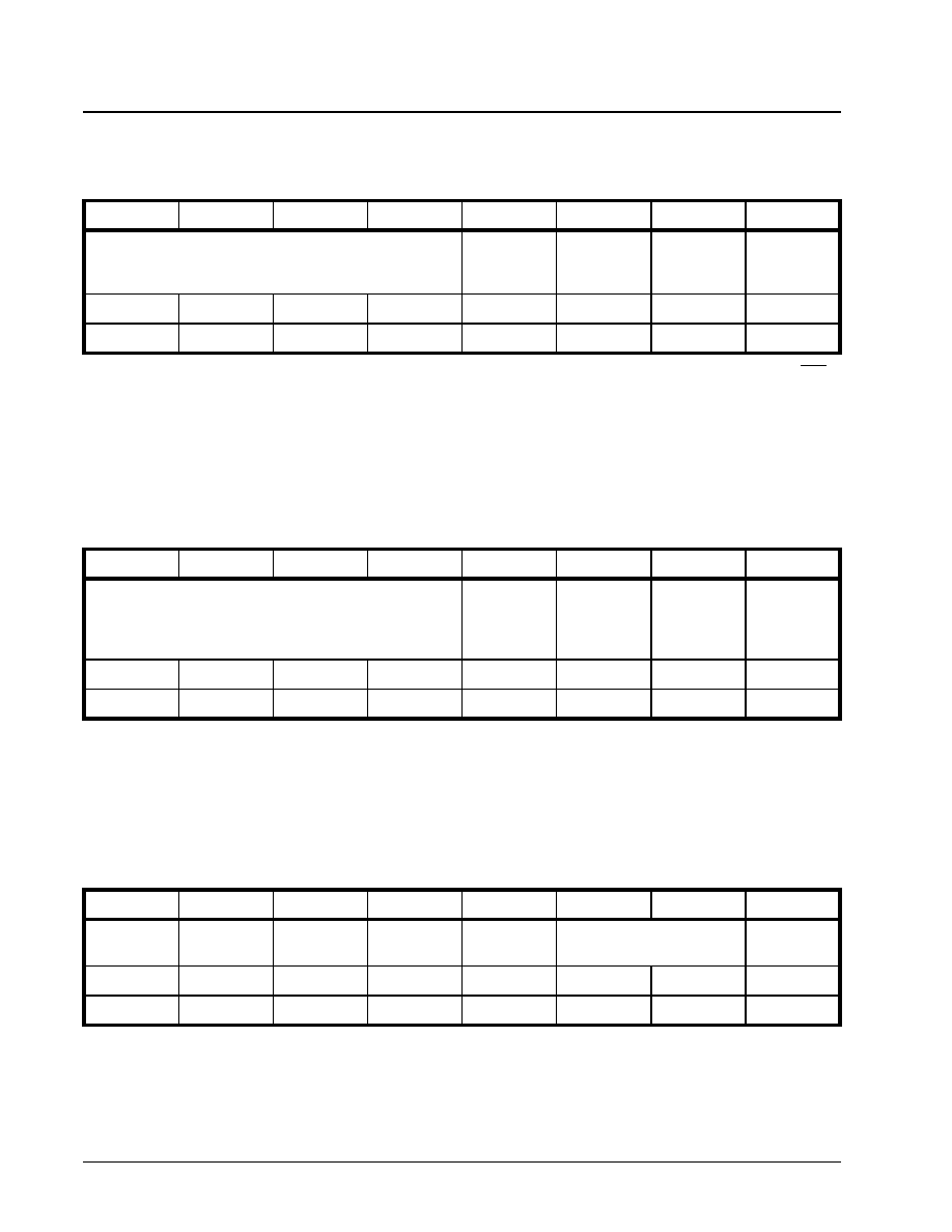
XRT7250
·Á
·Á
·Á
·Á
DS3/E3 FRAMER IC
REV. 1.1.1
328
the RxE3 Interrupt Enable Register - 2, as indicated
below.
Setting this bit-field to "1" enables this interrupt. Con-
versely, setting this bit-field to "0" disables this inter-
rupt.
Servicing the Change in Receive FERF Condition
Interrupt
Whenever the XRT7250 Framer IC detects this inter-
rupt, it will do all of the following.
∑ It will assert the Interrupt Request output pin (INT),
by driving it "Low".
∑ It will set Bit 3 (FERF Interrupt Status), within the
Rx E3 Interrupt Status Register - 2 to "1", as indi-
cated below.
Whenever the user's system encounters the Change
in Receive FERF Condition Interrupt, then it should
do the following.
1. It should determine the current state of the FERF
condition. Recall, that this interrupt can be gen-
erated, whenever the XRT7250 Framer IC
declares or clears the FERF defect. Hence, the
user can determine the current state of the LOS
defect by reading the state of Bit 0 (RxFERF)
within the Rx E3 Configuration and Status Regis-
ter - 2, as illustrated below.
5.3.6.2.7
The Detection of BIP-4 Error Interrupt
If the Detection of BIP-4 Error Interrupt is enabled,
then the XRT7250 Framer IC will generate an inter-
rupt, anytime the Receive E3 Framer block has de-
tected an error in the BIP-4 Nibble, within an incom-
ing E3 frame.
N
OTE
: This interrupt is only active if the XRT7250 Framer
IC has been configured to process the BIP-4 nibble within
each incoming and outbound E3 frame.
RXE3 INTERRUPT ENABLE REGISTER - 2 (ADDRESS = 0X13)
B
IT
7
B
IT
6
B
IT
5
B
IT
4
B
IT
3
B
IT
2
B
IT
1
B
IT
0
Not Used
FERF
Interrupt
Enable
BIP-4 Error
Interrupt
Enable
Framing Error
Interrupt
Enable
Not Used
R/W
RO
RO
RO
R/W
R/W
R/W
RO
0
0
0
0
0
0
0
0
RXE3 INTERRUPT STATUS REGISTER - 2 (ADDRESS = 0X15)
B
IT
7
B
IT
6
B
IT
5
B
IT
4
B
IT
3
B
IT
2
B
IT
1
B
IT
0
Not Used
FERF
Interrupt
Status
BIP-4
Error
Interrupt
Status
Framing
Error
Interrupt
Status
Not Used
RO
RO
RO
RO
RUR
RUR
RUR
RUR
0
0
0
0
1
0
0
0
RXE3 CONFIGURATION & STATUS REGISTER - 2 (ADDRESS = 0X11)
B
IT
7
B
IT
6
B
IT
5
B
IT
4
B
IT
3
B
IT
2
B
IT
1
B
IT
0
RxLOF
Algo
RxLOF
RxOOF
RxLOS
RxAIS
Not Used
RxFERF
R/W
RO
RO
RO
RO
RO
RO
RO
0
1
1
0
0
1
1
1

·Á
·Á
·Á
·Á
XRT7250
DS3/E3 FRAMER IC
REV. 1.1.1
329
Enabling and Disabling the Detection of FEBE
Event Interrupt
The user can enable or disable the Detection of BIP-4
Error' interrupt by writing the appropriate value into
Bit 2 (BIP-4 Interrupt Enable) within the Rx E3 Inter-
rupt Enable Register - 2, as indicated below.
Setting this bit-field to "1" enables this interrupt. Con-
versely, setting this bit-field to "0" disables this inter-
rupt.
Servicing the Detection of the BIP-4 Error Inter-
rupt
Whenever the XRT7250 Framer IC detects this inter-
rupt, it will do the following.
∑ It will assert the Interrupt Request output pin (INT),
by driving it "High".
∑ It will set the Bit 2 (BIP-4 Interrupt Status), within
the RxE3 Interrupt Status Register - 2 as indicated
below.
Whenever the Terminal Equipment encounters the
Detection of BIP-4 Error Interrupt, it should do the fol-
lowing.
∑ It should read the contents of the PMON Parity
Error Event Count Registers (located at Addresses
0x54 and 0x55) in order to determine the number of
BIP-4 Errors that have been received by the
XRT7250 Framer IC.
5.3.6.2.8
The Detection of Framing Error Inter-
rupt
If the Detection of Framing Error Interrupt is enabled,
then the XRT7250 Framer IC will generate an inter-
rupt, anytime the Receive E3 Framer block has re-
ceived an E3 frame with an incorrect FAS pattern val-
ue.
Enabling and Disabling the Detection of FEBE
Event Interrupt
The user can enable or disable the Detection of
Framing Error' interrupt by writing the appropriate val-
ue into Bit 1 (Framing Error Interrupt Enable) within
RXE3 INTERRUPT ENABLE REGISTER - 2 (ADDRESS = 0X13)
B
IT
7
B
IT
6
B
IT
5
B
IT
4
B
IT
3
B
IT
2
B
IT
1
B
IT
0
Not Used
FERF
Interrupt
Enable
BIP-4 Error
Interrupt
Enable
Framing Error
Interrupt
Enable
Not Used
R/W
RO
RO
RO
R/W
R/W
R/W
RO
0
0
0
0
0
X
0
0
RXE3 INTERRUPT STATUS REGISTER - 2 (ADDRESS = 0X15)
B
IT
7
B
IT
6
B
IT
5
B
IT
4
B
IT
3
B
IT
2
B
IT
1
B
IT
0
Not Used
FERF
Interrupt
Status
BIP-4
Error
Interrupt
Status
Framing
Error
Interrupt
Status
Not Used
RO
RO
RO
RO
RUR
RUR
RUR
RUR
0
0
0
0
0
1
0
0
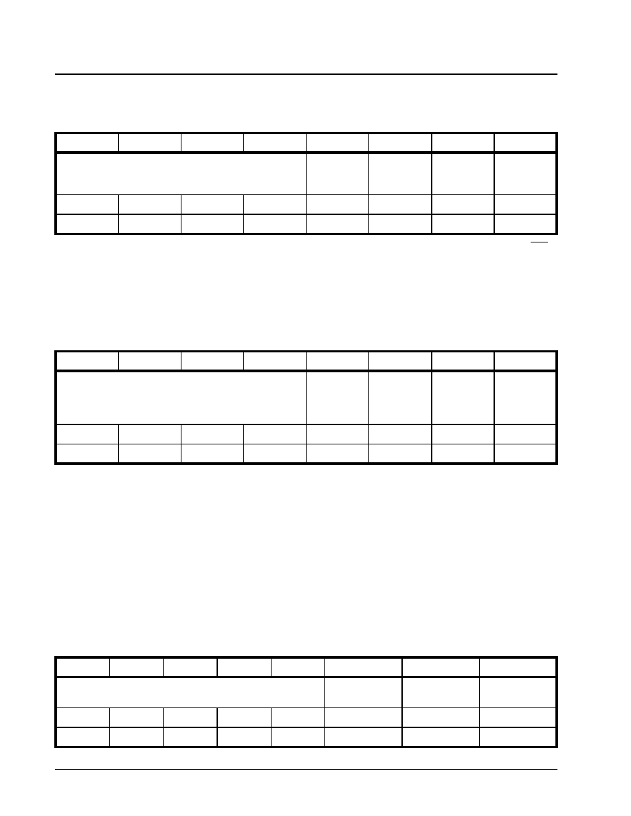
XRT7250
·Á
·Á
·Á
·Á
DS3/E3 FRAMER IC
REV. 1.1.1
330
the Rx E3 Interrupt Enable Register - 2, as indicated
below.
Setting this bit-field to "1" enables this interrupt. Con-
versely, setting this bit-field to "0" disables this inter-
rupt.
Servicing the Detection of Framing Error Interrupt
Whenever the XRT7250 Framer IC detects this inter-
rupt, it will do the following.
∑ It will assert the Interrupt Request output pin (INT),
by driving it "High".
∑ It will set the Bit 1 (Framing Error Interrupt Status),
within the RxE3 Interrupt Status Register - 2 as
indicated below.
Whenever the Terminal Equipment encounters the
Detection of Framing Error Interrupt, it should do the
following.
∑ It should read the contents of the PMON Framing
Bit/Byte Error Count Registers (located at
Addresses 0x52 and 0x53) in order to determine
the number of Framing errors that have been
received by the XRT7250 Framer IC.
5.3.6.2.9
The Receipt of New LAPD Message
Interrupt
If the Receive LAPD Message Interrupt is enabled,
then the XRT7250 Framer IC will generate an inter-
rupt anytime the Receive HDLC Controller block has
received a new LAPD Message frame from the Re-
mote Terminal Equipment, and has stored the con-
tents of this message into the Receive LAPD Mes-
sage buffer.
Enabling/Disabling the Receive LAPD Message
Interrupt
The user can enable or disable the Receive LAPD
Message Interrupt by writing the appropriate data into
Bit 1 (RxLAPD Interrupt Enable) within the Rx E3
LAPD Control Register, as indicated below.
RXE3 INTERRUPT ENABLE REGISTER - 2 (ADDRESS = 0X13)
B
IT
7
B
IT
6
B
IT
5
B
IT
4
B
IT
3
B
IT
2
B
IT
1
B
IT
0
Not Used
FERF
Interrupt
Enable
BIP-4 Error
Interrupt
Enable
Framing Error
Interrupt
Enable
Not Used
R/W
RO
RO
RO
R/W
R/W
R/W
RO
0
0
0
0
0
0
X
0
RXE3 INTERRUPT STATUS REGISTER - 2 (ADDRESS = 0X15)
B
IT
7
B
IT
6
B
IT
5
B
IT
4
B
IT
3
B
IT
2
B
IT
1
B
IT
0
Not Used
FERF
Interrupt
Status
BIP-4
Error
Interrupt
Status
Framing
Error
Interrupt
Status
Not Used
RO
RO
RO
RO
RUR
RUR
RUR
RUR
0
0
0
0
0
0
0
0
RXE3 LAPD CONTROL REGISTER (ADDRESS = 0X18)
B
IT
7
B
IT
6
B
IT
5
B
IT
4
B
IT
3
B
IT
2
B
IT
1
B
IT
0
Not Used
RxLAPD
Enable
RxLAPD
Interrupt Enable
RxLAPD
Interrupt Enable
RO
RO
RO
RO
RO
R/W
R/W
RUR
0
0
0
0
0
0
0
0

·Á
·Á
·Á
·Á
XRT7250
DS3/E3 FRAMER IC
REV. 1.1.1
331
Writing a "1" into this bit-field enables the Receive
LAPD Message Interrupt. Conversely, writing a "0"
into this bit-field disables the Receive LAPD Message
Interrupt.
Servicing the Receive LAPD Message Interrupt
Whenever the XRT7250 Framer IC generates this in-
terrupt, it will do the following.
∑ It will assert the Interrupt Request output pin (INT),
by driving it "Low".
∑ It will set Bit 0 (RxLAPD Interrupt Status), within the
Rx E3 LAPD Control register to "1", as indicated
below.
∑ It will write the contents of the newly Received
LAPD Message into the Receive LAPD Message
buffer (located at 0xDE through 0x135).
Whenever the Terminal Equipment encounters the
Receive LAPD Message Interrupt, then it should read
out the contents of the Receive LAPD Message buff-
er, and respond accordingly.
RXE3 LAPD CONTROL REGISTER (ADDRESS = 0X18)
B
IT
7
B
IT
6
B
IT
5
B
IT
4
B
IT
3
B
IT
2
B
IT
1
B
IT
0
Not Used
RxLAPD
Enable
RxLAPD
Interrupt Enable
RxLAPD
Interrupt Enable
RO
RO
RO
RO
RO
R/W
R/W
RUR
0
0
0
0
0
0
0
0
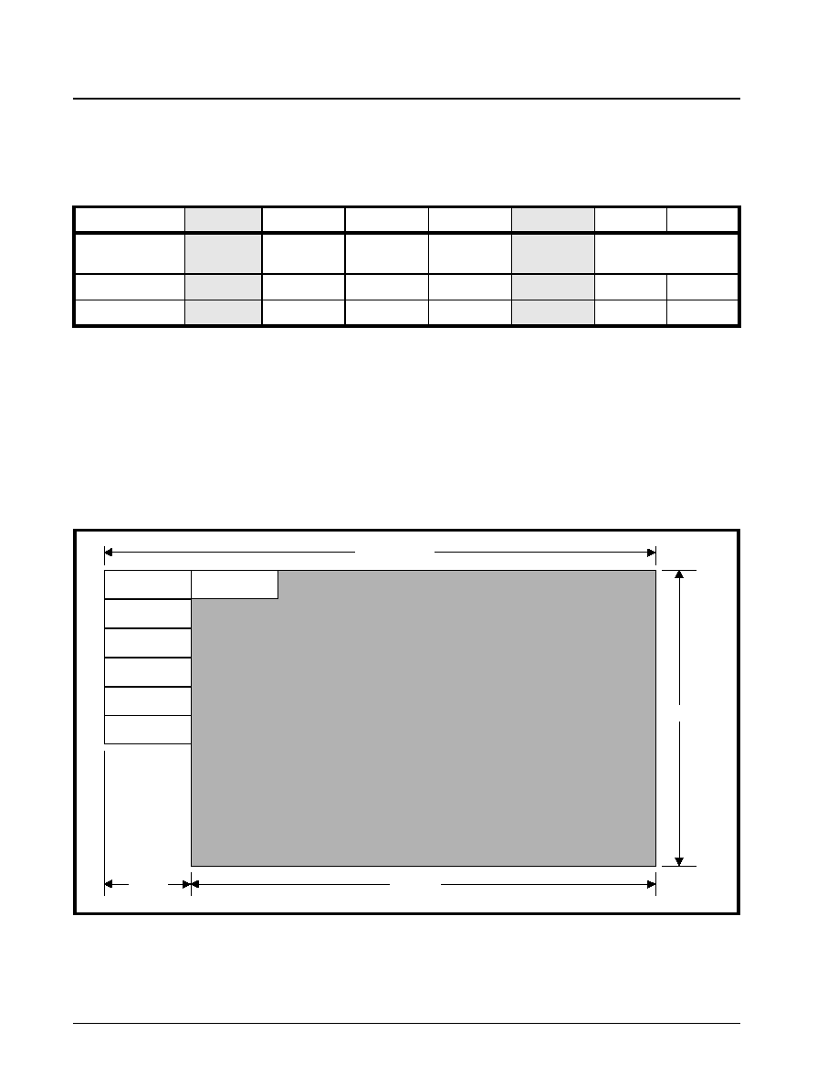
XRT7250
·Á
·Á
·Á
·Á
DS3/E3 FRAMER IC
REV. 1.1.1
332
6.0
E3/ITU-T G.832 OPERATION OF THE
XRT7250
Configuring the XRT7250 to Operate in the E3,
ITU-T G.832 Mode
The XRT7250 can be configured to operate in the E3/
ITU-T G.832 Mode by writing a "0" into bit-field 6 and
a "1" into bit-field 2, within the Framer Operating
Mode register, as illustrated below.
Prior to describing the functional blocks within the
Transmit and Receive Sections of the XRT7250, it is
important to describe the E3, ITU-T G.832 framing
format.
6.1
D
ESCRIPTION
OF
THE
E3, ITU-T G.832 F
RAMES
AND
A
SSOCIATED
O
VERHEAD
B
YTES
The role of the various overhead bytes are best de-
scribed by discussing the E3, ITU-T G.832 Frame
Format as a whole. The E3, ITU-T G.832 Frame con-
tains 537 bytes, of which 7 bytes are overhead and
the remaining 530 bytes are payload bytes.
These 537 octets are arranged in 9 rows of 60 col-
umns each, except for the last three rows which con-
tain only 59 columns. The frame repetition rate for
this type of E3 frame is 8000 times per second, there-
by resulting in the standard E3 bit rate of 34.368
Mbps. Figure 154 presents an illustration of the E3,
ITU-T G.832 Frame Format.
6.1.1
Definition of the Overhead Bytes
The seven (7) overhead bytes are shown in
Figure 154, as FA1, FA2, EM, TR, MA, NR and GC.
Each of these Overhead Bytes are further defined be-
low.
FRAMER OPERATING MODE REGISTER (ADDRESS = 0X00)
B
IT
7
B
IT
6
B
IT
5
B
IT
4
B
IT
3
B
IT
2
B
IT
1
B
IT
0
Local Loopback
DS3/E3*
Internal
LOS Enable
RESET
Interrupt
Enable Reset
Frame Format
TimRefSel[1:0]
R/W
R/W
R/W
R/W
R/W
R/W
R/W
R/W
x
0
x
0
x
1
x
x
F
IGURE
154. I
LLUSTRATION
OF
THE
E3, ITU-T G.832 F
RAMING
F
ORMAT
.
FA1
FA2
EM
TR
MA
1 Byte
59 Bytes
60 Columns
9 Rows
530 Octet Payload
GC
NR
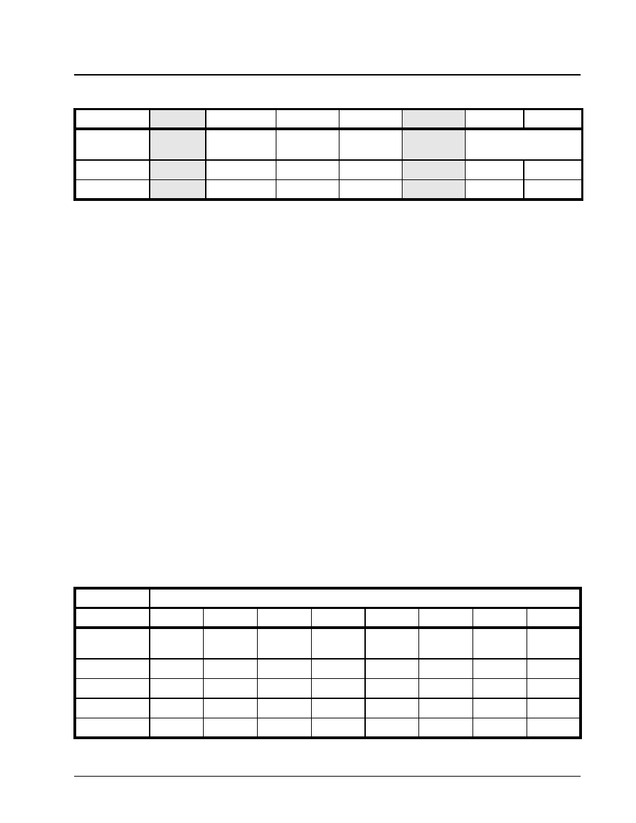
·Á
·Á
·Á
·Á
XRT7250
DS3/E3 FRAMER IC
REV. 1.1.1
333
6.1.1.1
Frame Alignment (FA1 and FA2) Bytes
FA1 and FA2 are known as the frame alignment
bytes. The Receive E3 Framer, while trying to ac-
quire or maintain framing synchronization with its in-
coming E3 frames, will attempt to locate these two
bytes. FA1 is assigned the value "0xF6" and FA2 is
assigned the value "0x28".
6.1.1.2
Error Monitor (EM) Byte
The EM byte contains the results of BIP-8 (Bit-Inter-
leaved Parity) calculations over an entire E3 frame.
The Bit Interleaved Parity (BIP-8) byte field supports
error detection, during the transmission of E3 frames,
between the Local Terminal Equipment and the Re-
mote Terminal Equipment.
The Transmit E3 Framer will compute the BIP-8 value
over the 537 octet structure, within each E3 frame.
The resulting BIP-8 value is then inserted into the EM
byte-field within the very next E3 frame. BIP-8 is an
eight bit code in which the nth bit of the BIP-8 code
reflects the even-parity bit calculated with the nth bit
of each of the 537 octets within the E3 frame. Thus,
the BIP-8 value presents the results for 8 separate
even-bit parity calculations.
The Receive E3 Framer will compute its own version
of the EM bytes for each E3 frame that it receives. Af-
terwards, it will compare the value of its locally com-
puted EM byte with the EM byte that it receives in the
very next E3 frame. If the two EM byte values are
equal, then the Receive E3 Framer will conclude that
this E3 frame was received in an error-free manner.
Further, the Receive E3 Framer will block will inform
the Remote Terminal Equipment of this fact by having
the Local Terminal Equipment set the FEBE (Far-
End-Block Error) bit, within the MA Byte of an Out-
bound E3 frame (to the Remote Terminal Equipment)
to "0". Please see Section 5.1.1 for a discussion of
the MA Byte.
However, if the Receive E3 Framer block detects an
error in the incoming EM byte, then it will conclude
that the corresponding E3 frame is errored. Further,
the Receive E3 Framer block will inform the Remote
Terminal (e.g., the source of this erred E3 frame) of
this fact by having the Local Terminal Equipment
(e.g., the Transmit E3 Framer block) set the FEBE bit,
within an Outbound E3 frame (destined to the Re-
mote Terminal) to "1".
N
OTE
: A detailed discussion on the practical use of the EM
byte is presented in Section 5.2.2.
6.1.1.3
The Trail-Trace Buffer (TTB) Byte
This byte-field is used to repetitively transmit a Trail-
access point identifier so that a trail receiving terminal
can verify its continued connection to the intended
transmitter. The trail access point identifier uses the
16-byte numbering format as tabulated in Table 68.
FRAMER OPERATING MODE REGISTER (ADDRESS = 0X00)
B
IT
7
B
IT
6
B
IT
5
B
IT
4
B
IT
3
B
IT
2
B
IT
1
B
IT
0
Local Loopback
DS3/E3*
Internal LOS
Enable
RESET
Interrupt
Enable Reset
Frame Format
TimRefSel[1:0]
R/W
R/W
R/W
R/W
R/W
R/W
R/W
R/W
x
1
x
0
x
x
x
x
T
ABLE
68: D
EFINITION
OF
THE
T
RAIL
T
RACE
B
UFFER
B
YTES
,
WITHIN
T
HE
E3, ITU-T G.832 F
RAMING
F
ORMAT
T
RAIL
T
RACE
B
ITS
B
YTE
N
UMBER
B
IT
7
B
IT
6
B
IT
5
B
IT
4
B
IT
3
B
IT
2
B
IT
1
B
IT
0
1 (Frame Start
Marker)
1
C6
C5
C4
C3
C2
C1
C0
2
X
X
X
X
X
X
X
X
*
X
X
X
X
X
X
X
X
*
X
X
X
X
X
X
X
X
16
X
X
X
X
X
X
X
X

XRT7250
·Á
·Á
·Á
·Á
DS3/E3 FRAMER IC
REV. 1.1.1
334
The first byte of this 16-byte string is a frame start
marker and is typically of the form [1, C6, C5, C4, C3,
C2, C1, C0]. The "1" in the MSB (most significant bit)
of this first byte is used to identify this byte as the
frame start marker (e.g., the first byte of the 16-byte
Trail Trace Buffer Sequence). The bits: C6 through
C0 are the results of a CRC-7 calculation over the
previous 16-byte frame. The subsequent 15 bytes
are used for the transport of 15 ASCII characters re-
quired for the E.164 numbering format.
6.1.1.4
Maintenance and Adaptation (MA) Byte
The MA byte is responsible for carrying the FERF
(Far-End Receive Failure) and the FEBE (Far-End
Block Error) status indicators from one terminal to an-
other. The MA byte-field also carries the Payload
Type, the Payload Dependent and the Timing Marker
indicators. The byte format for the MA byte is pre-
sented below.
Bit 7 - FERF (Far-End Receive Failure)
If the Receive E3 Framer block (at a Local Terminal)
is experiencing problems receiving E3 frame data
from a Remote Terminal (e.g., an LOS, OOF or AIS
condition), then it will inform the Remote Terminal
Equipment of this fact by commanding the Local
Transmit E3 Framer block to set the FERF bit-field
(within the MA byte) of an Outbound E3 frame, to "1".
The Local Transmit E3 Framer block will continue to
set the FERF bit-field (within the subsequent Out-
bound E3 frames) to "1" until the Receive E3 Framer
block no longer experiences problems in receiving the
E3 frame data. If the Remote Terminal Equipment re-
ceives a certain number of consecutive E3 frames,
with the FERF bit-field set to "1", then the Remote
Terminal Equipment will interpret this signaling as an
indication of a Far-End Receive Failure (e.g., a prob-
lem with the Local Terminal Equipment).
Conversely, if the Receive E3 Framer block (at a Lo-
cal Terminal Equipment) is not experiencing any
problems receiving E3 frame data from a Remote Ter-
minal Equipment, then it will also inform the Remote
Terminal Equipment of this fact by commanding the
Local Transmit E3 Framer block to set the FERF bit-
field (within the MA byte-field) of an Outbound E3
frame (which is destined for the Remote Terminal) to
"0". The Remote Terminal Equipment will interpret
this form of signaling as an indication of a normal op-
eration.
N
OTE
: A detailed discussion into the practical use of the
FERF bit-field is presented in Section 5.2.4.2.
Bit 6 - FEBE (Far-End Block Error)
If a Local Receive E3 Framer block detects an error in
the EM byte, within an incoming E3 frame that it has
received from the Remote Terminal Equipment, then
it will inform the Remote Terminal Equipment of this
error by commanding the Local Transmit E3 Framer
block to set the FEBE bit-field (within the MA byte-
field) of an Outbound E3 frame (which is destined for
the Remote Terminal Equipment) to "1". The Remote
Terminal Equipment will interpret this signaling as an
indication that the E3 frames that it is transmitting
back out to the Local Receive E3 Framer block are
erred.
Conversely, if the Local Receive E3 Framer block
does not detect any errors in the EM byte, within the
incoming E3 frame, then it will also inform the Re-
mote Terminal Equipment of this fact by commanding
the Local Transmit E3 Framer block to set the FEBE
bit-field of an Outbound E3 frame (which is destined
for the Remote Terminal Equipment) to "0".
N
OTE
: A detailed discussion into the practical use of the
FEBE bit-field is presented in Section 5.2.4.2.
Bits 5 - 3 Payload Type
These bit-fields indicates to the Remote Terminal
Equipment, what kind of data is being transported in
the 530 bytes of E3 frame payload data. Some of the
defined payload type values are tabulated in Table 69.
THE MAINTENANCE AND ADAPTATION (MA) BYTE FORMAT
B
IT
7
B
IT
6
B
IT
5
B
IT
4
B
IT
3
B
IT
2
B
IT
1
B
IT
0
FERF
FEBE
Payload Type
Payload Dependent
Timing Marker

·Á
·Á
·Á
·Á
XRT7250
DS3/E3 FRAMER IC
REV. 1.1.1
335
Bits 2 - 1 Payload Dependent
To be provided later.
Bit 0 - Timing Marker
This bit-field is set to "0" to indicate that the timing
source is traceable to a Primary Reference Clock.
Otherwise, this bit-field is set to "1".
6.1.1.5
The Network Operator (NR) Byte
The NR byte or the GC byte can be configured to
transport LAP-D Message frame octets from the
LAPD Transmitter to the LAPD Receiver (of the Re-
mote Terminal Equipment) at a data rate of 64kbps (1
byte per E3 frame).
If the user opts not to use the NR byte to transport
these LAPD Message frames, then the Transmit E3
Framer block will read in the contents of the TxNR
Byte Register (Address = 0x37), and insert this value
into the NR byte-field of each Outbound E3 frame.
The Receive E3 Framer block will read in the contents
of the NR byte-field within each incoming E3 frame
and will write it into the RxNR Byte register. Conse-
quently, the user can determine the value of the NR
byte, within the most recently received E3 frame by
reading the Rx NR Byte Register (Address = 0x1A).
6.1.1.6
The General Purpose Communica-
tions Channel (GC) Byte
The NR byte or the GC byte can be configured to
transport LAPD Message frames from the LAPD
Transmitter to the LAPD Receiver (of the Remote Ter-
minal Equipment) at a data rate of 64kbps (1 byte per
E3 frame).
If the user opts not to use the GC byte to transport
these LAPD Message frames, then the Transmit E3
Framer block will read in the contents of the Tx GC
Byte Register (Address = 0x35), and insert this value
into the GC byte-field of each Outbound E3 frame.
The Receive E3 Framer block will read in the contents
of the GC byte-field, within each incoming E3 frame,
and will write it into the RxGC Byte register. Conse-
quently, the user can determine the value of the GC
byte, within the most recently received E3 frame, by
reading the Rx GC Byte register (Address = 0x1B).
6.2
T
HE
T
RANSMIT
S
ECTION
OF
THE
XRT7250 (E3
M
ODE
O
PERATION
)
When the XRT7250 has been configured to operate
in the E3, ITU-T G.832 Mode, the Transmit Section of
the XRT7250 consists of the following functional
blocks.
∑ Transmit Payload Data Input Interface block
∑ Transmit Overhead Data Input Interface block
∑ Transmit E3 Framer block
∑ Transmit HDLC Controller block
∑ Transmit LIU Interface block
Figure 155 presents a simple illustration of the Trans-
mit Section of the XRT7250 Framer IC.
T
ABLE
69: A L
ISTING
OF
THE
V
ARIOUS
P
AYLOAD
T
YPE
V
ALUES
AND
THEIR
CORRESPONDING
M
EANING
P
AYLOAD
T
YPE
V
ALUE
M
EANING
000
Unequipped
001
Equipped
010
ATM Cells
011
SDH TU-12s
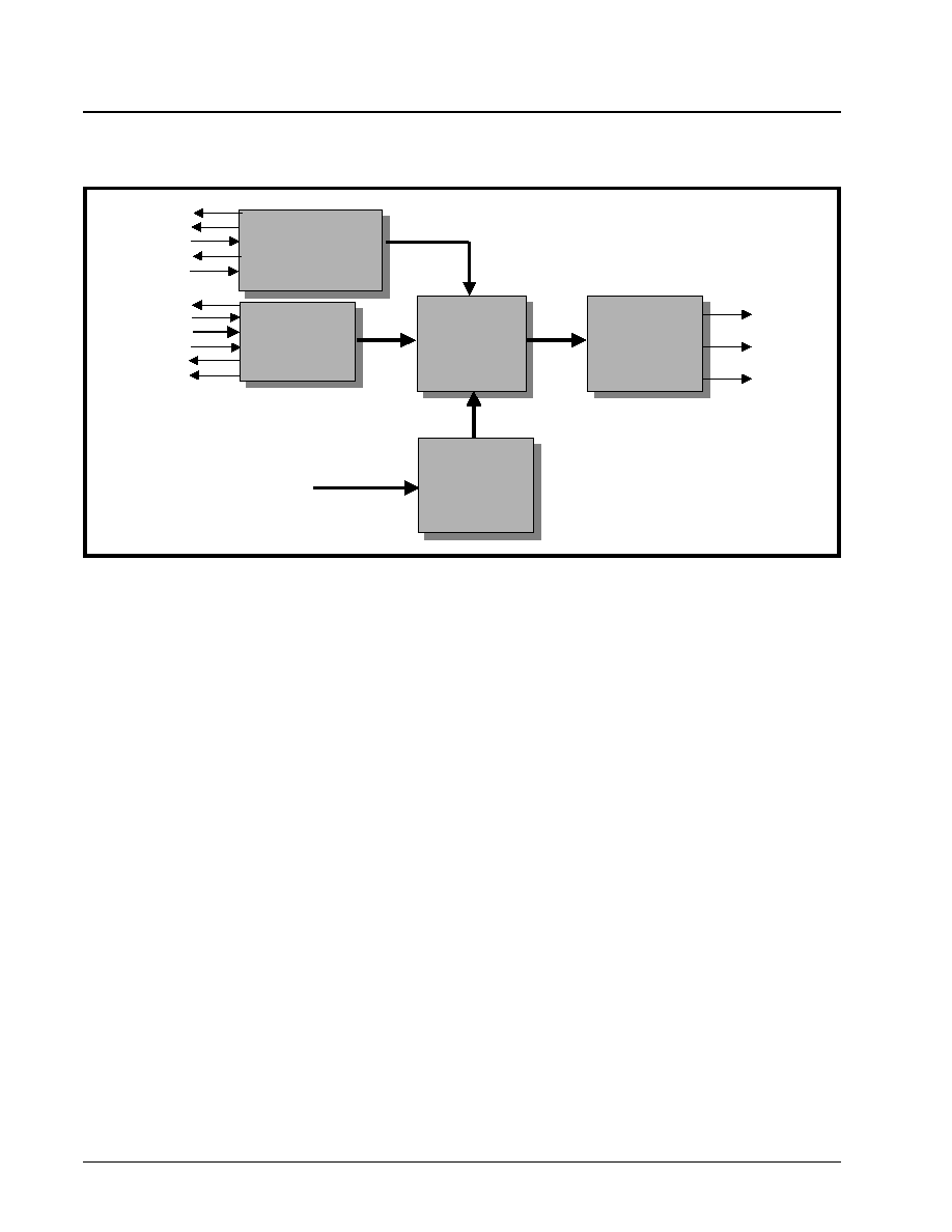
XRT7250
·Á
·Á
·Á
·Á
DS3/E3 FRAMER IC
REV. 1.1.1
336
Each of these functional blocks will be discussed in
detail in this document.
6.2.1
The Transmit Payload Data Input Interface
Block
Figure 156 presents a simple illustration of the Trans-
mit Payload Data Input Interface block.
F
IGURE
155. A S
IMPLE
I
LLUSTRATION
OF
THE
T
RANSMIT
S
ECTION
,
WITHIN
THE
XRT7250,
WHEN
IT
HAS
BEEN
CON
-
FIGURED
TO
OPERATE
IN
THE
E3 M
ODE
Transmit
Payload Data
Input
Interface Block
Transmit DS3/E3
Framer Block
Transmit LIU
Interface
Block
TxSer
TxNib[3:0]
TxInClk
TxPOS
TxNEG
TxLineClk
Transmit Overhead
Input
Interface Block
TxOHClk
TxOHIns
TxOHInd
TxOH
TxOHEnable
TxOHFrame
TxNibClk
TxFrame
Tx E3 HDLC
Controller/Buffer
Tx E3 HDLC
Controller/Buffer
From Microprocessor
Interface Block
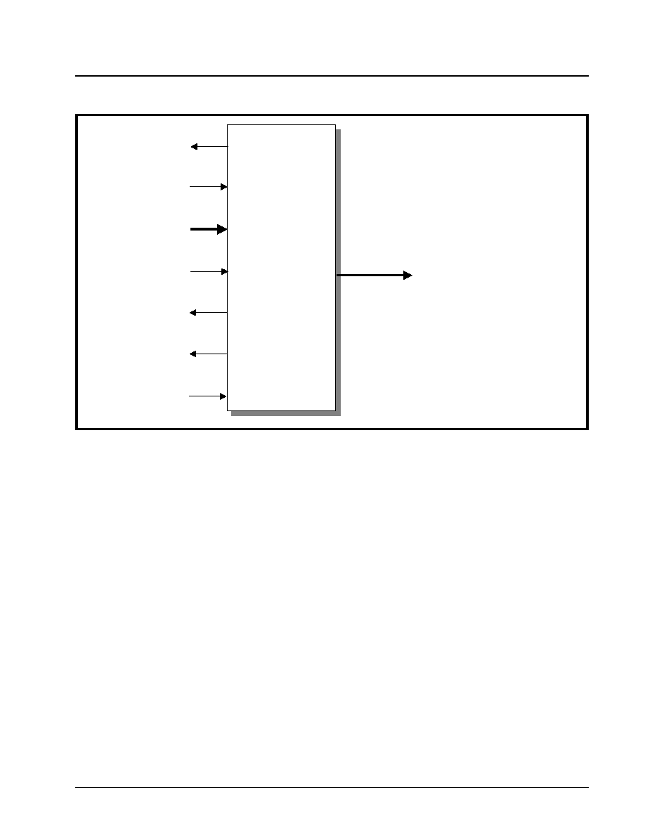
·Á
·Á
·Á
·Á
XRT7250
DS3/E3 FRAMER IC
REV. 1.1.1
337
Each of the input and output pins of the Transmit Pay-
load Data Input Interface are listed in Table 70 and
described below. The exact role that each of these
inputs and output pins assume, for a variety of operat-
ing scenarios are described throughout this section.
F
IGURE
156. A S
IMPLE
I
LLUSTRATION
OF
THE
T
RANSMIT
P
AYLOAD
D
ATA
I
NPUT
I
NTERFACE
B
LOCK
Transmit Payload
Data Input
Interface Block
Transmit Payload
Data Input
Interface Block
TxOH_Ind
TxSer
TxNib[3:0]
TxInClk
TxNibClk
TxFrame
TxFrameRef
To Transmit E3 Framer Block

XRT7250
·Á
·Á
·Á
·Á
DS3/E3 FRAMER IC
REV. 1.1.1
338
T
ABLE
70: L
ISTING
AND
D
ESCRIPTION
OF
THE
PINS
ASSOCIATED
WITH
THE
T
RANSMIT
P
AYLOAD
D
ATA
I
NPUT
I
NTERFACE
S
IGNAL
N
AME
T
YPE
D
ESCRIPTION
TxSer
Input
Transmit Serial Payload Data Input Pin:
If the user opts to operate the XRT7250 in the serial mode, then the Terminal Equipment is
expected to apply the payload data (that is to be transported via the Outbound E3 data stream)
to this input pin. The XRT7250 will sample the data that is at this input pin upon the rising edge
either the RxOutClk or the TxInClk signal (whichever is appropriate).
N
OTE
: This signal is only active if the NibInt input pin is pulled "Low".
TxNib[3:0]
Input
Transmit Nibble-Parallel Payload Data Input pins:
If the user opts to operate the XRT7250 in the Nibble-Parallel mode, then the Terminal Equip-
ment is expected to apply the payload data (that is to be transported via the Outbound E3 data
stream) to these input pins. The XRT7250 will sample the data that is at these input pins upon
the rising edge of the TxNibClk signal.
N
OTE
: These pins are only active if the NibInt input pin is pulled "High".
TxInClk
Input
Transmit Section Timing Reference Clock Input pin:
The Transmit Section of the XRT7250 can be configured to use this clock signal as the Timing
Reference. If the user has made this configuration selection, then the XRT7250 will use this
clock signal to sample the data on the TxSer input pin.
N
OTE
: If this configuration is selected, then a 34.368 MHz clock signal must be applied to this
input pin.
TxNibClk
Output Transmit Nibble Mode Output
If the user opts to operate the XRT7250 in the Nibble-Parallel mode, then the XRT7250 will
derive this clock signal from the selected Timing Reference for the Transmit Section of the chip
(e.g., either the TxInClk or the RxLineClk signals).
The XRT7250 will use this signal to sample the data on the TxNib[3:0] input pins.
TxOHInd
Output Transmit Overhead Bit Indicator Output:
This output pin will pulse "High" one-bit period prior to the time that the Transmit Section of the
XRT7250 will be processing an Overhead bit. The purpose of this output pin is to warn the Ter-
minal Equipment that, during the very next bit-period, the XRT7250 is going to be processing
an Overhead bit and will be ignoring any data that is applied to the TxSer input pin.
TxFrame
Output Transmit End of Frame Output Indicator:
The Transmit Section of the XRT7250 will pulse this output pin "High" (for one bit-period), when
the Transmit Payload Data Input Interface is processing the last bit of a given E3 frame.
The purpose of this output pin is to alert the Terminal Equipment that it needs to begin trans-
mission of a new E3 frame to the XRT7250 (e.g., to permit the XRT7250 to maintain Transmit
E3 framing alignment control over the Terminal Equipment).
TxFrameRef
Input
Transmit Frame Reference Input:
The XRT7250 permits the user to configure the Transmit Section to use this input pin as a
frame reference. If the user makes this configuration selection, then the Transmit Section will
initiate its transmission of a new E3 frame, upon the rising edge of this signal.
The purpose of this input pin is to permit the Terminal Equipment to maintain Transmit E3 Fram-
ing alignment control over the XRT7250.
RxOutClk
Output Loop-Timed Timing Reference Clock Output pin:
The Transmit Section of the XRT7250 can be configured to use the RxLineClk signal as the
Timing Reference (e.g., loop-timing). If the user has made this configuration selection, then the
XRT7250 will:
∑
Output a 34.368 MHz clock signal via this pin, to the Terminal Equipment.
∑
Sample the data on the TxSer input pin, upon the rising edge of this clock signal.

·Á
·Á
·Á
·Á
XRT7250
DS3/E3 FRAMER IC
REV. 1.1.1
339
Operation of the Transmit Payload Data Input In-
terface
The Transmit Terminal Input Interface is extremely
flexible, in that it permits the user to make the follow-
ing configuration options.
∑ The Serial or the Nibble-Parallel Interface Mode
∑ The Loop-Timing or the TxInClk (Local Timing)
Mode
Further, if the XRT7250 has been configured to oper-
ate in the TxInClk mode, then the user has two addi-
tional options.
∑ The XRT7250 is the Frame Master (e.g., it dictates
when the Terminal Equipment will initiate the trans-
mission of data within a new E3 frame).
∑ The XRT7250 is the Frame Slave (e.g., the Termi-
nal Equipment will dictate when the XRT7250 ini-
tiates the transmission of a new E3 frame).
Given these three set of options, the Transmit Termi-
nal Input Interface can be configured to operate in
one of the six (6) following modes.
∑ Mode 1 - Serial/Loop-Timed Mode
∑ Mode 2 - Serial/Local-Timed/Frame Slave Mode
∑ Mode 3 - Serial/Local-Timed/Frame Master Mode
∑ Mode 4 - Nibble/Loop-Timed Mode
∑ Mode 5 - Nibble/Local-Timed/Frame Slave Mode
∑ Mode 6 - Nibble/Local-Timed/Frame Master Mode
Each of these modes are described, in detail, below.
6.2.1.1
Mode 1 - The Serial/Loop-Timing Mode
The Behavior of the XRT7250
If the XRT7250 has been configured to operate in this
mode, then the XRT7250 will behave as follows.
A. Loop-Timing (Uses the RxLineClk signal as the
Timing Reference)
Since the XRT7250 is configured to operate in the
loop-timed mode, the Transmit Section (of the
XRT7250) will use the RxLineClk input clock signal
(e.g., the Recovered Clock signal, from the LIU) as its
timing source. When the XRT7250 is operating in this
mode it will do the following.
1. It will ignore any signal at the TxInClk input pin.
2. The XRT7250 will output a 34.368MHz clock sig-
nal via the RxOutClk output pin. This clock signal
functions as the Transmit Payload Data Input
Interface block clock signal.
3. The XRT7250 will use the rising edge of the
RxOutClk signal to latch in the data residing on
the TxSer input pin.
B. Serial Mode
The XRT7250 will accept the E3 payload data from
the Terminal Equipment, in a serial-manner, via the
TxSer input pin The Transmit Payload Data Input In-
terface will latch this data into its circuitry, on the ris-
ing edge of the RxOutClk output clock signal.
C. Delineation of Outbound E3 frames
The XRT7250 will pulse the TxFrame output pin
"High" for one bit-period, coincident with the
XRT7250 processing the last bit of a given E3 frame.
D. Sampling of Payload Data, from the Terminal
Equipment
In Mode 1, the XRT7250 will sample the data at the
TxSer input, on the rising edge of RxOutClk.
Interfacing the Transmit Payload Data Input Inter-
face block of the XRT7250 to the Terminal Equip-
ment for Mode 1 Operation
Figure 157 presents an illustration of the Transmit
Payload Data Input Interface block (within the
XRT7250) being interfaced to the Terminal Equip-
ment, for Mode 1 operation.
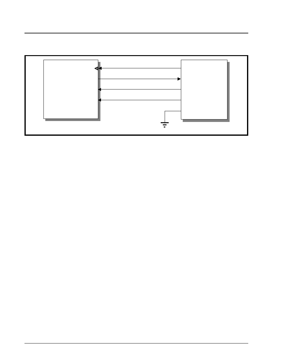
XRT7250
·Á
·Á
·Á
·Á
DS3/E3 FRAMER IC
REV. 1.1.1
340
Mode 1 Operation of the Terminal Equipment
When the XRT7250 is operating in this mode it will
function as the source of the 34.368MHz clock signal.
This clock signal will be used as the Terminal Equip-
ment Interface clock by both the XRT7250 IC and the
Terminal Equipment.
The Terminal Equipment will serially output the pay-
load data of the Outbound E3 data stream via its
E3_Data_Out pin. The Terminal Equipment will up-
date the data on the E3_Data_Out pin upon the rising
edge of the 34.368 MHz clock signal, at its
E3_Clock_In input pin (as depicted in Figures 19 and
20).
The XRT7250 will latch the Outbound E3 data stream
(from the Terminal Equipment) on the rising edge of
the RxOutClk signal.
The XRT7250 will indicate that it is processing the
last bit, within a given Outbound E3 frame, by pulsing
its TxFrame output pin "High" for one bit-period.
When the Terminal Equipment detects this pulse at its
Tx_Start_of_Frame input, it is expected to begin
transmission of the very next Outbound E3 frame to
the XRT7250 via the E3_Data_Out (or TxSer pin).
Finally, the XRT7250 will indicate that it is about to
process an overhead bit by pulsing the TxOH_Ind
output pin "High" one bit period prior to its processing
of an OH (Overhead) bit. In Figure 157, the
TxOH_Ind output pin is connected to the
E3_Overhead_Ind input pin, of the Terminal Equip-
ment. Whenever the E3_Overhead_Ind pin is pulsed
"High" the Terminal Equipment is expected to not
transmit a E3 payload bit upon the very next clock
edge. Instead, the Terminal Equipment is expected to
delay its transmission of the very next payload bit, by
one clock cycle.
The behavior of the signals, between the XRT7250
and the Terminal Equipment, for E3 Mode 1 operation
is illustrated in Figure 158.
F
IGURE
157. I
LLUSTRATION
OF
THE
T
ERMINAL
E
QUIPMENT
BEING
INTERFACED
TO
THE
T
RANSMIT
P
AYLOAD
D
ATA
I
NPUT
I
NTERFACE
BLOCK
OF
THE
XRT7250
FOR
M
ODE
1 (S
ERIAL
/L
OOP
-T
IMED
) O
PERATION
Terminal Equipment
XRT7250 E3 Framer
E3_Data_Out
E3_Clock_In
Tx_Start_of_Frame
E3_Overhead_Ind
TxSer
RxOutClk
TxFrame
TxOH_Ind
NibInt
34.368 MHz
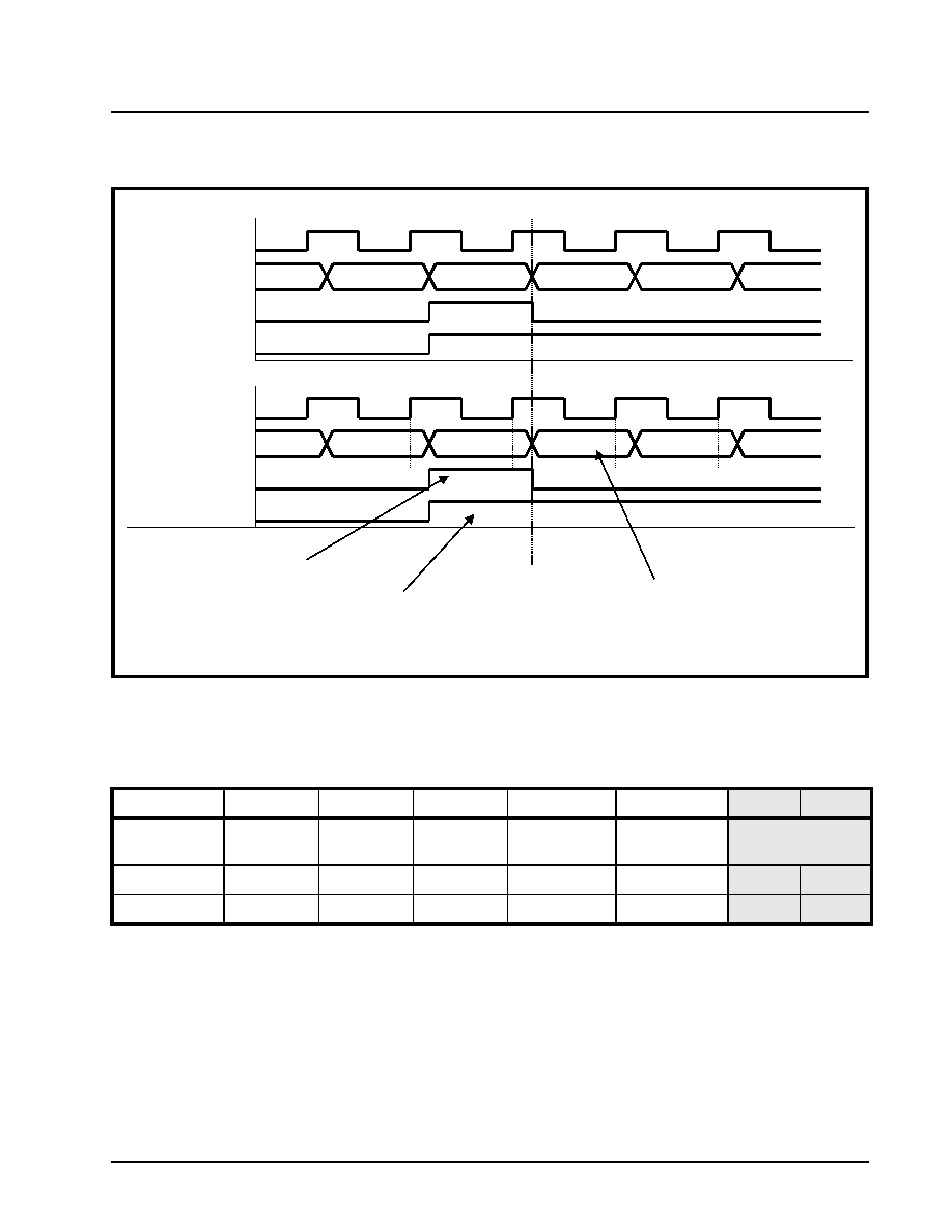
·Á
·Á
·Á
·Á
XRT7250
DS3/E3 FRAMER IC
REV. 1.1.1
341
How to configure the XRT7250 into the Serial/
Loop-Timed/Non-Overhead Interface Mode
1. Set the NibIntf input pin "Low".
2. Set the TimRefSel[1:0] bit fields (within the
Framer Operating Mode Register) to "00" as illus-
trated below.
3. Interface the XRT7250, to the Terminal Equip-
ment, as illustrated in Figure 157.
6.2.1.2
Mode 2 - The Serial/Local-Timed/
Frame-Slave Mode Behavior of the XRT7250
If the XRT7250 has been configured to operate in this
mode, then the XRT7250 will function as follows.
A. Local Timing - Uses the TxInClk signal as the
Timing Reference
In this mode, the Transmit Section of the XRT7250
will use the TxInClk signal as its timing reference.
B. Serial Mode
The XRT7250 will receive the E3 payload data, in a
serial manner, via the TxSer input pin. The Transmit
Payload Data Input Interface (within the XRT7250)
will latch this data into its circuitry, on the rising edge
of the TxInClk input clock signal.
C. Delineation of Outbound E3 frames (Frame
Slave Mode)
The Transmit Section of the XRT7250 will use the Tx-
InClk input as its timing reference, and will use the
F
IGURE
158. B
EHAVIOR
OF
THE
T
ERMINAL
I
NTERFACE
SIGNALS
BETWEEN
THE
T
RANSMIT
P
AYLOAD
D
ATA
I
NPUT
I
NTERFACE
BLOCK
OF
THE
XRT7250
AND
THE
T
ERMINAL
E
QUIPMENT
(
FOR
M
ODE
1 O
PERATION
)
Terminal Equipment Signals
E3_Clock_In
E3_Data_Out
Tx_Start_of_Frame
E3_Overhead_Ind
XRT7250 Transmit Payload Data I/F Signals
RxOutClk
TxSer
TxFrame
TxOH_Ind
Payload[4238]
Payload[4239]
FA1, Bit 7
FA1, Bit 6
Payload[4238]
Payload[4239]
FA1, Bit 7
FA1, Bit 6
Note: The FA1 byte will not be processed by the
Transmit Payload Data Input Interface.
E3 Frame Number N
E3 Frame Number N + 1
Note: RxFrame pulses high to denote
E3 Frame Boundary.
Note: TxOH_Ind pulses high for
16 bit periods in order to
denote Overhead Data
(e.g., the FA1 and FA2 bytes)
FRAMER OPERATING MODE REGISTER (ADDRESS = 0X00)
B
IT
7
B
IT
6
B
IT
5
B
IT
4
B
IT
3
B
IT
2
B
IT
1
B
IT
0
Local Loopback
DS3/E3*
Internal LOS
Enable
RESET
Interrupt
Enable Reset
Frame Format
TimRefSel[1:0]
R/W
R/W
R/W
R/W
R/W
R/W
R/W
R/W
0
0
1
0
1
0
0
0
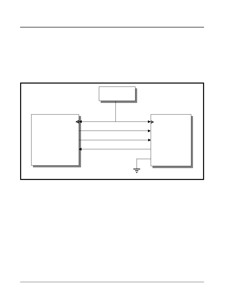
XRT7250
·Á
·Á
·Á
·Á
DS3/E3 FRAMER IC
REV. 1.1.1
342
TxFrameRef input signal as its framing reference. In
other words, the Transmit Section of the XRT7250 will
initiate frame generation upon the rising edge of the
TxFrameRef input signal).
D. Sampling of payload data, from the Terminal
Equipment
In Mode 2, the XRT7250 will sample the data, at the
TxSer input pin, on the rising edge of TxInClk.
Interfacing the Transmit Payload Data Input Inter-
face block of the XRT7250 to the Terminal Equip-
ment for Mode 2 Operation
Figure 159 presents an illustration of the Transmit
Payload Data Input Interface block (within the
XRT7250) being interfaced to the Terminal Equip-
ment, for Mode 2 operation.
Mode 2 Operation of the Terminal Equipment
As shown in Figure 159, both the Terminal Equipment
and the XRT7250 will be driven by an external
34.368MHz clock signal. The Terminal Equipment
will receive the 34.368MHz clock signal via its
E3_Clock_In input pin, and the XRT7250 Framer IC
will receive the 34.368MHz clock signal via the TxIn-
Clk input pin.
The Terminal Equipment will serially output the pay-
load data of the Outbound E3 data stream, via the
E3_Data_Out output pin, upon the rising edge of the
signal at the E3_Clock_In input pin. (Note: The
E3_Data_Out output pin of the Terminal Equipment is
electrically connected to the TxSer input pin). The
XRT7250 Framer IC will latch the data, residing on
the TxSer input line, on the rising edge of the TxInClk
signal.
In this case, the Terminal Equipment has the respon-
sibility of providing the framing reference signal by
pulsing its Tx_Start_of_Frame output signal (and in
turn, the TxFrameRef input pin of the XRT7250),
"High" for one-bit period, coincident with the first bit of
a new E3 frame. Once the XRT7250 detects the ris-
ing edge of the input at its TxFrameRef input pin, it
will begin generation of a new E3 frame.
N
OTES
:
1. In this case, the Terminal Equipment is controlling
the start of Frame Generation, and is therefore
referred to as the Frame Master. Conversely, since
the XRT7250 does not control the generationi of a
new E3 frame, but is rather driven by the Terminal
Equipment, the XRT7250 is referred to as the
Frame Slave.
2. If the user opts to configure the XRT7250 to oper-
ate in Mode 2, it is imperative that the
Tx_Start_of_Frame (or TxFrameRef) signal is syn-
chronized to the TxInClk input clock signal.
Finally, the XRT7250 will pulse its TxOH_Ind output
pin, one bit-period prior to it processing a given over-
head bit, within the Outbound E3 frame. Since the
TxOH_Ind output pin (of the XRT7250) is electrically
F
IGURE
159. I
LLUSTRATION
OF
THE
T
ERMINAL
E
QUIPMENT
BEING
INTERFACED
TO
THE
T
RANSMIT
P
AYLOAD
D
ATA
I
NPUT
I
NTERFACE
BLOCK
OF
THE
XRT7250
FOR
M
ODE
2 (S
ERIAL
/L
OCAL
-T
IMED
/F
RAME
-S
LAVE
) O
PERATION
Terminal Equipment
XRT7250 E3 Framer
E3_Data_Out
E3_Clock_In
Tx_Start_of_Frame
E3_Overhead_Ind
TxSer
TxInClk
TxFrameRef
TxOH_Ind
NibInt
34.368 MHz Clock
Source
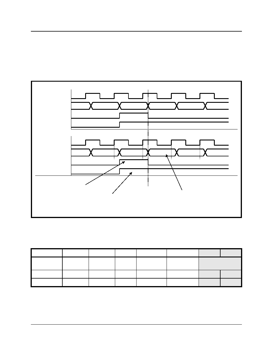
·Á
·Á
·Á
·Á
XRT7250
DS3/E3 FRAMER IC
REV. 1.1.1
343
connected to the E3_Overhead_Ind, whenever the
XRT7250 pulses the TxOH_Ind output pin "High", it
will also be driving the E3_Overhead_Ind input pin (of
the Terminal Equipment) "High". Whenever the Ter-
minal Equipment detects this pin toggling "High", it
should delay transmission of the very next E3 frame
payload bit by one clock cycle.
The behavior of the signals between the XRT7250
and the Terminal Equipment for E3 Mode 2 Operation
is illustrated in Figure 160.
How to configure the XRT7250 to operate in this
mode.
1. Set the NibIntf input pin "Low".
2. Set the TimRefSel[1:0] bit-fields (within the
Framer Operating Mode Register) to "01" as
depicted below.
3. Interface the XRT7250, to the Terminal Equip-
ment, as illustrated in Figure 159.
6.2.1.3
Mode 3 - The Serial/Local-Timed/
Frame-Master ModeBehavior of the XRT7250
If the XRT7250 has been configured to operate in this
mode, then the XRT7250 will function as follows.
A. Local Timed - Uses the TxInClk signal as the
Timing Reference
F
IGURE
160. B
EHAVIOR
OF
THE
T
ERMINAL
I
NTERFACE
SIGNALS
BETWEEN
THE
XRT7250
AND
THE
T
ERMINAL
E
QUIPMENT
(M
ODE
2 O
PERATION
)
Terminal Equipment Signals
E3_Clock_In
E3_Data_Out
Tx_Start_of_Frame
E3_Overhead_Ind
XRT7250 Transmit Payload Data I/F Signals
TxInClk
TxSer
TxFrame
TxOH_Ind
Payload[4238]
Payload[4239]
FA1, Bit 7
FA1, Bit 6
Payload[4238]
Payload[4239]
FA1, Bit 7
FA1, Bit 6
Note: The FA1 byte will not be processed by the
Transmit Payload Data Input Interface.
E3 Frame Number N
E3 Frame Number N + 1
Note: RxFrame pulses high to denote
E3 Frame Boundary.
Note: TxOH_Ind pulses high for
16 bit periods in order to
denote Overhead Data
(e.g., the FA1 and FA2 bytes)
FRAMER OPERATING MODE REGISTER (ADDRESS = 0X00)
B
IT
7
B
IT
6
B
IT
5
B
IT
4
B
IT
3
B
IT
2
B
IT
1
B
IT
0
Local Loopback
DS3/E3*
Internal LOS
Enable
RESET
Interrupt
Enable Reset
Frame Format
TimRefSel[1:0]
R/W
R/W
R/W
R/W
R/W
R/W
R/W
R/W
0
0
1
0
1
0
0
1

XRT7250
·Á
·Á
·Á
·Á
DS3/E3 FRAMER IC
REV. 1.1.1
344
In this mode, the Transmit Section of the XRT7250
will use the TxInClk signal as its timing reference.
B. Serial Mode
The XRT7250 will receive the E3 payload data, in a
serial manner, via the TxSer input pin. The Transmit
Payload Data Input Interface (within the XRT7250)
will latch this data into its circuitry, on the rising edge
of the TxInClk input clock signal.
C. Delineation of Outbound DS3 frames (Frame
Master Mode)
The Transmit Section of the XRT7250 will use the Tx-
InClk signal as its timing reference, and will initiate E3
frame generation, asynchronously with respect to any
externally applied signal. The XRT7250 will pulse its
TxFrame output pin "High" whenever its it processing
the very last bit-field within a given E3 frame.
D. Sampling of payload data, from the Terminal
Equipment
In Mode 3, the XRT7250 will sample the data, at the
TxSer input pin, on the rising edge of TxInClk.
Interfacing the Transmit Payload Data Input Inter-
face block of the XRT7250 to the Terminal Equip-
ment for Mode 3 Operation
Figure 161 presents an illustration of the Transmit
Payload Data Input Interface block (within the
XRT7250) being interfaced to the Terminal Equip-
ment, for Mode 3 operation.
Mode 3 Operation of the Terminal Equipment
In Figure 161, both the Terminal Equipment and the
XRT7250 are driven by an external 34.368 MHz clock
signal. This clock signal is connected to the
E3_Clock_In input of the Terminal Equipment and the
TxInClk input pin of the XRT7250.
The Terminal Equipment will serially output the pay-
load data on its E3_Data_Out output pin, upon the
rising edge of the signal at the E3_Clock_In input pin.
Similarly, the XRT7250 will latch the data, residing on
the TxSer input pin, on the rising edge of TxInClk.
The XRT7250 will pulse the TxFrame output pin
"High" for one bit-period, coincident while it is pro-
cessing the last bit-field within a given Outbound E3
frame. The Terminal Equipment is expected to moni-
tor the TxFrame signal (from the XRT7250) and to
place the first bit, within the very next Outbound E3
frame on the TxSer input pin.
N
OTE
: In this case, the XRT7250 dictates exactly when the
very next E3 frame will be generated. The Terminal Equip-
ment is expected to respond appropriately by providing the
XRT7250 with the first bit of the new E3 frame, upon
demand. Hence, in this mode, the XRT7250 is referred to
as the Frame Master and the Terminal Equipment is
referred to as the Frame Slave.
Finally, the XRT7250 will pulse its TxOH_Ind output
pin, one bit-period prior to it processing a given over-
F
IGURE
161. I
LLUSTRATION
OF
THE
T
ERMINAL
E
QUIPMENT
BEING
INTERFACED
TO
THE
T
RANSMIT
P
AYLOAD
D
ATA
I
NPUT
I
NTERFACE
BLOCK
OF
THE
XRT7250
FOR
M
ODE
3 (S
ERIAL
/L
OCAL
-T
IMED
/F
RAME
-M
ASTER
) O
PERATION
Terminal Equipment
XRT7250 E3 Framer
E3_Data_Out
E3_Clock_In
Tx_Start_of_Frame
E3_Overhead_Ind
TxSer
TxInClk
TxFrame
TxOH_Ind
NibInt
34.368 MHz Clock
Source
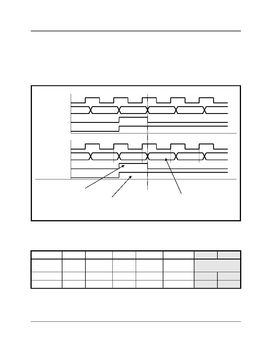
·Á
·Á
·Á
·Á
XRT7250
DS3/E3 FRAMER IC
REV. 1.1.1
345
head bit, within the Outbound E3 frame. Since the
TxOH_Ind output pin of the XRT7250 is electrically
connected to the E3_Overhead_Ind whenever the
XRT7250 pulses the TxOH_Ind output pin "High", it
will also be driving the E3_Overhead_Ind input pin (of
the Terminal Equipment) "High". Whenever the Ter-
minal Equipment detects this pin toggling "High", it
should delay transmission of the very next DS3 frame
payload bit by one clock cycle.
The behavior of the signal between the XRT7250 and
the Terminal Equipment for E3 Mode 3 Operation is il-
lustrated in Figure 162.
How to configure the XRT7250 to operate in this
mode.
1. Set the NibIntf input pin "Low".
2. Set the TimRefSel[1:0] bit-fields (within the
Framer Operating Mode Register) to "01".
3. Interface the XRT7250, to the Terminal Equip-
ment, as illustrated in Figure 162.
6.2.1.4
Mode 4 - The Nibble-Parallel/Loop-
Timed Mode Behavior of the XRT7250
If the XRT7250 has been configured to operate in this
mode, then the XRT7250 will behave as follows.
A. Looped Timing (Uses the RxLineClk as the
Timing Reference)
F
IGURE
162. B
EHAVIOR
OF
THE
T
ERMINAL
I
NTERFACE
SIGNALS
BETWEEN
THE
XRT7250
AND
THE
T
ERMINAL
E
QUIP
-
MENT
(E3 M
ODE
3 O
PERATION
)
Terminal Equipment Signals
E3_Clock_In
E3_Data_Out
Tx_Start_of_Frame
E3_Overhead_Ind
XRT7250 Transmit Payload Data I/F Signals
TxInClk
TxSer
TxFrame
TxOH_Ind
Payload[4238]
Payload[4239]
FA1, Bit 7
FA1, Bit 6
Payload[4238]
Payload[4239]
FA1, Bit 7
FA1, Bit 6
Note: The FA1 byte will not be processed by the
Transmit Payload Data Input Interface.
E3 Frame Number N
E3 Frame Number N + 1
Note: RxFrame pulses high to denote
E3 Frame Boundary.
Note: TxOH_Ind pulses high for
16 bit periods in order to
denote Overhead Data
(e.g., the FA1 and FA2 bytes)
FRAMER OPERATING MODE REGISTER (ADDRESS = 0X00)
B
IT
7
B
IT
6
B
IT
5
B
IT
4
B
IT
3
B
IT
2
B
IT
1
B
IT
0
Local Loopback
DS3/E3*
Internal LOS
Enable
RESET
Interrupt
Enable Reset
Frame Format
TimRefSel[1:0]
R/W
R/W
R/W
R/W
R/W
R/W
R/W
R/W
0
0
1
0
1
0
0
0
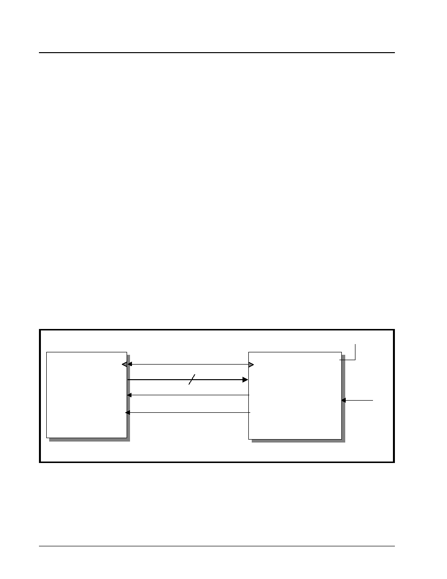
XRT7250
·Á
·Á
·Á
·Á
DS3/E3 FRAMER IC
REV. 1.1.1
346
In this mode, the Transmit Section of the XRT7250
will use the RxLineClk signal as its timing reference.
When the XRT7250 is operating in the Nibble-Mode,
it will internally divide the RxLineClk signal, by a fac-
tor of four (4) and will output this signal via the TxNib-
Clk output pin.
B. Nibble-Parallel Mode
The XRT7250 will accept the E3 payload data, from
the Terminal Equipment in a nibble-parallel manner,
via the TxNib[3:0] input pins. The Transmit Terminal
Equipment Input Interface block will latch this data in-
to its circuitry, on the rising edge of the TxNibClk out-
put signal.
C. Delineation of the Outbound E3 frames
The XRT7250 will pulse the TxNibFrame output pin
"High" for one bit-period, coincident with the
XRT7250 processing the last nibble of a given E3
frame.
D. Sampling of payload data, from the Terminal
Equipment
In Mode 4, the XRT7250 will sample the data, at the
TxNib[3:0] input pins, on the third rising edge of the
RxOutClk clock signal, following a pulse in the TxNib-
Clk signal (see Figure 164).
N
OTE
: The TxNibClk signal, from the XRT7250, operates
nominally at 11.184 MHz (e.g., 44.736 MHz divided by 4).
However, for reasons described below, TxNibClk effectively
operates at a lower clock frequency. The Transmit Payload
Data Input Interface is only used to accept the payload
data, which is intended to be carried by Outbound DS3
frames. The Transmit Payload Data Input Interface is not
designed to accommodate the entire DS3 data stream.
The E3 Frame consists of 537 bytes or 1074 nibbles.
Therefore, the XRT7250 will supply 1074 TxNibClk
pulses between the rising edges of two consecutive
TxNibFrame pulses. The E3 Frame repetition rate is
8.0kHz. Hence, 1074 TxNibClk pulses for each E3
frame period amounts to TxNibClk running at approx-
imately 8.592 MHz. The method by which the 1074
TxNibClk pulses are distributed throughout the E3
frame period is presented below.
Nominally, the Transmit Section within the XRT7250
will generate a TxNibClk pulse for every 4 RxOutClk
(or TxInClk) periods.
Interfacing the Transmit Payload Data Input Inter-
face block of the XRT7250 to the Terminal Equip-
ment for Mode 4 Operation
Figure 163 presents an illustration of the Transmit
Payload Data Input Interface block (within the
XRT7250) being interfaced to the Terminal Equip-
ment, for Mode 4 Operation.
Mode 4 Operation of the Terminal Equipment
When the XRT7250 is operating in this mode, it will
function as the source of the 8.592MHz (e.g., the
34.368MHz clock signal divided by 4) clock signal
that will be used as the Terminal Equipment Interface
clock by both the XRT7250 and the Terminal Equip-
ment.
The Terminal Equipment will output the payload data
of the Outbound E3 data stream via its
E3_Data_Out[3:0] pins on the rising edge of the
8.592MHz clock signal at the E3_Nib_Clock_In input
pin.
The XRT7250 will latch the Outbound E3 data stream
(from the Terminal Equipment) on the rising edge of
F
IGURE
163. I
LLUSTRATION
OF
THE
T
ERMINAL
E
QUIPMENT
BEING
INTERFACED
TO
THE
T
RANSMIT
P
AYLOAD
D
ATA
I
NPUT
I
NTERFACE
BLOCK
OF
THE
XRT7250
FOR
M
ODE
4 (N
IBBLE
-P
ARALLEL
/L
OOP
-T
IMED
) O
PERATION
Terminal Equipment
XRT7250 E3 Framer
E3_Data_Out[3:0]
E3_Nib_Clock_In
Tx_Start_of_Frame
TxNib[3:0]
TxNibClk
TxNibFrame
NibInt
VCC
4
RxLineClk
34.368MHz
8.592 MHz
TxOH_Ind
E3_Overhead_Ind

·Á
·Á
·Á
·Á
XRT7250
DS3/E3 FRAMER IC
REV. 1.1.1
347
the TxNibClk output clock signal. The XRT7250 will
indicate that it is processing the last nibble, within a
given E3 frame, by pulsing its TxNibFrame output pin
"High" for one TxNibClk clock period. When the Ter-
minal Equipment detects a pulse at its
Tx_Start_of_Frame input pin, it is expected to trans-
mit the first nibble, of the very next Outbound E3
frame to the XRT7250 via the E3_Data_Out[3:0] (or
TxNib[3:0] pins).
Finally, for the Nibble-Parallel Mode operation, the
XRT7250 will pulse the TxOHInd output pin "High" for
a total of 14 nibble periods (e.g., for the 7 overhead
bytes, within each of the E3, ITU-T G.832 frames). At
the beginning of an E3 frame, the XRT7250 will pulse
the TxOHInd output pin "High" for 4 nibble periods.
These four nibbles represent the "FA1" and "FA2"
bytes within each E3 frame. Throughout the remain-
der of the E3 framing period, the XRT7250 will pulse
the TxOHInd output pin 5 times. The width (or dura-
tion) of each of these pulses will be two nibbles.
Clearly, each of these 5 pulses corresponds to the
five remaining overhead bytes, within the E3, ITU-T
G.832 framing structure.
The behavior of the signals between the XRT7250
and the Terminal Equipment for E3 Mode 4 Operation
is illustrated in Figure 164.
How to configure the XRT7250 into Mode 4
1. Set the NibIntf input pin "High".
2. Set the TimRefSel[1:0] bit-fields (within the
Framer Operating Mode Register) to "00" as illus-
trated below.
F
IGURE
164. B
EHAVIOR
OF
THE
T
ERMINAL
I
NTERFACE
SIGNALS
BETWEEN
THE
XRT7250
AND
THE
T
ERMINAL
E
QUIP
-
MENT
(M
ODE
4 O
PERATION
)
Terminal Equipment Signals
RxOutClk
Tx_Start_of_Frame
E3_Nib_Clock_In
E3_Data_Out[3:0]
Payload Nibble [1059]
Overhead Nibble [0]
XRT7250 Transmit Payload Data I/F Signals
E3 Frame Number N
E3 Frame Number N + 1
Note: TxNibFrame pulses high to denote
E3 Frame Boundary.
RxOutClk
TxNibFrame
TxNibClk
TxNib[3:0]
Nibble [1059]
Overhead Nibble [0]
E3_Overhead_Ind
TxOH_Ind
TxOH_Ind pulses high for 4 Nibble periods
FRAMER OPERATING MODE REGISTER (ADDRESS = 0X00)
B
IT
7
B
IT
6
B
IT
5
B
IT
4
B
IT
3
B
IT
2
B
IT
1
B
IT
0
Local Loopback
DS3/E3*
Internal LOS
Enable
RESET
Interrupt
Enable Reset
Frame Format
TimRefSel[1:0]

XRT7250
·Á
·Á
·Á
·Á
DS3/E3 FRAMER IC
REV. 1.1.1
348
3. Interface the XRT7250, to the Terminal Equip-
ment, as illustrated in Figure 163.
6.2.1.5
Mode 5 - The Nibble-Parallel/Local-
Time/Frame-Slave Interface Mode Behavior of the
XRT7250
If the XRT7250 has been configured to operate in this
mode, then the XRT7250 will function as follows:
A. Local Timing - Uses the TxInClk signal as the
Timing Reference
In this mode, the Transmit Section of the XRT7250
will use the TxInClk signal at its timing reference.
Further, the chip will internally divide the TxInClk
clock signal by a factor of 4 and will output this divid-
ed clock signal via the TxNibClk output pin. The
Transmit Terminal Equipment Input Interface block
(within the XRT7250) will use the rising edge of the
TxNibClk signal, to latch the data, residing on the Tx-
Nib[3:0] into its circuitry.
B. Nibble-Parallel Mode
The XRT7250 will accept the DS3 payload data, from
the Terminal Equipment, in a parallel manner, via the
TxNib[3:0] input pins. The Transmit Terminal Equip-
ment Input Interface will latch this data into its circuit-
ry, on the rising edge of the TxNibClk output signal.
C. Delineation of Outbound E3 Frames
The Transmit Section will use the TxInClk input signal
as its timing reference and will use the TxFrameRef
input signal as its Framing Reference (e.g., the Trans-
mit Section of the XRT7250 initiates frame generation
upon the rising edge of the TxFrameRef signal).
D. Sampling of payload data, from the Terminal
Equipment
In Mode 5, the XRT7250 will sample the data, at the
TxNib[3:0] input pins, on the third rising edge of the
TxInClk clock signal, following a pulse in the TxNibClk
signal (see Figure 166).
N
OTE
: The TxNibClk signal, from the XRT7250 operates
nominally at 8.592 MHz (e.g., 34.368 MHz divided by 4).
Interfacing the Transmit Payload Data Input Inter-
face block of the XRT7250 to the Terminal Equip-
ment for Mode 5 Operation
Figure 165 presents an illustration of the Transmit
Payload Data Input Interface block (within the
XRT7250) being interfaced to the Terminal Equip-
ment, for Mode 5 Operation.
R/W
R/W
R/W
R/W
R/W
R/W
R/W
R/W
0
0
1
0
1
0
0
0
FRAMER OPERATING MODE REGISTER (ADDRESS = 0X00)
B
IT
7
B
IT
6
B
IT
5
B
IT
4
B
IT
3
B
IT
2
B
IT
1
B
IT
0
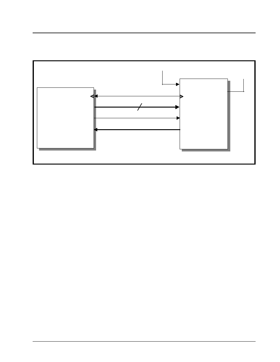
·Á
·Á
·Á
·Á
XRT7250
DS3/E3 FRAMER IC
REV. 1.1.1
349
Mode 5 Operation of the Terminal Equipment
In Figure 165 both the Terminal Equipment and the
XRT7250 will be driven by an external 8.592MHz
clock signal. The Terminal Equipment will receive the
8.592MHz clock signal via the E3_Nib_Clock_In input
pin. The XRT7250 will output the 8.592MHz clock
signal via the TxNibClk output pin.
The Terminal Equipment will serially output the data
on the E3_Data_Out[3:0] pins, upon the rising edge
of the signal at the E3_Clock_In input pin.
N
OTE
: The E3_Data_Out[3:0] output pins of the Terminal
Equipment is electrically connected to the TxNib[3:0] input
pins.
The XRT7250 will latch the data, residing on the Tx-
Nib[3:0] input pins, on the rising edge of the TxNibClk
signal.
In this case, the Terminal Equipment has the respon-
sibility of providing the framing reference signal by
pulsing the Tx_Start_of_Frame output pin (and in
turn, the TxFrameRef input pin of the XRT7250)
"High" for one bit-period, coincident with the first bit of
a new E3 frame. Once the XRT7250 detects the ris-
ing edge of the input at its TxFrameRef input pin, it
will begin generation of a new E3 frame.
Finally, the XRT7250 will always internally generate
the Overhead bits, when it is operating in both the E3
and Nibble-parallel modes. The XRT7250 will pull the
TxOHInd input pin "Low".
The behavior of the signals between the XRT7250
and the Terminal Equipment for E3 Mode 5 Operation
is illustrated in Figure 166.
F
IGURE
165. I
LLUSTRATION
OF
THE
T
ERMINAL
E
QUIPMENT
BEING
INTERFACED
TO
THE
T
RANSMIT
P
AYLOAD
D
ATA
I
NPUT
I
NTERFACE
BLOCK
OF
THE
XRT7250
FOR
M
ODE
5 (N
IBBLE
-P
ARALLEL
/L
OCAL
-T
IME
/F
RAME
-S
LAVE
) O
PERA
-
TION
Terminal Equipment
XRT7250 E3 Framer
E3_Data_Out[3:0]
E3_Nib_Clock_In
Tx_Start_of_Frame
TxNib[3:0]
TxNibClk
TxFrameRef
NibInt
VCC
4
34.368MHz Clock Source
TxInClk
8.592MHz
E3_Overhead_Ind
TxOH_Ind
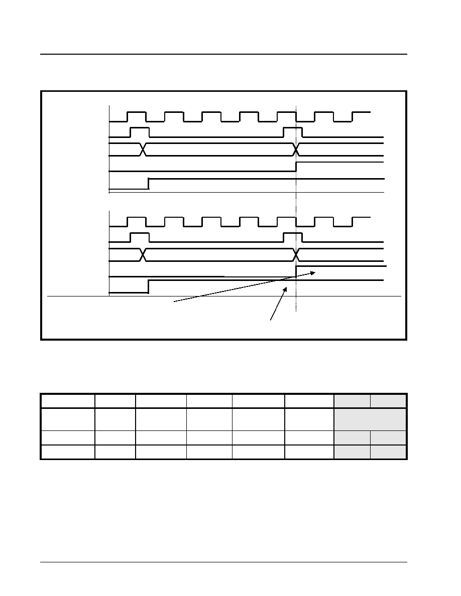
XRT7250
·Á
·Á
·Á
·Á
DS3/E3 FRAMER IC
REV. 1.1.1
350
How to configure the XRT7250 into Mode 5
1. Set the NibIntf input pin "High".
2. Set the TimRefSel[1:0] bit-fields (within the
Framer Operating Mode Register) to "01" as illus-
trated below.
3. Interface the XRT7250, to the Terminal Equip-
ment, as illustrated in Figure 165.
6.2.1.6
Mode 6 - The Nibble-Parallel/Local-
Timed/Frame-Master Interface Mode Behavior of
the XRT7250
If the XRT7250 has been configured to operate in this
mode, then the XRT7250 will function as follows:
A. Local Timing - Uses the TxInClk signal as the
Timing Reference
In this mode, the Transmit Section of the XRT7250
will use the TxInClk signal at its timing reference.
Further, the chip will internally divide the TxInClk
clock signal by a factor of 4 and will output this divid-
ed clock signal via the TxNibClk output pin. The
Transmit Terminal Equipment Input Interface block
(within the XRT7250) will use the rising edge of the
TxNibClk signal, to latch the data, residing on the Tx-
Nib[3:0] into its circuitry.
B. Nibble-Parallel Mode
F
IGURE
166. B
EHAVIOR
OF
THE
T
ERMINAL
I
NTERFACE
SIGNALS
BETWEEN
THE
XRT7250
AND
THE
T
ERMINAL
E
QUIPMENT
(E3 M
ODE
5 O
PERATION
)
Terminal Equipment Signals
RxOutClk
Tx_Start_of_Frame
E3_Nib_Clock_In
E3_Data_Out[3:0]
Payload Nibble [1059]
Overhead Nibble [0]
XRT7250 Transmit Payload Data I/F Signals
E3 Frame Number N
E3 Frame Number N + 1
Note: Terminal Equipment pulses
"TxFrameRef" in order to denote
the E3 Frame Boundary.
RxOutClk
TxFrameRef
TxNibClk
TxNib[3:0]
Nibble [1059]
Overhead Nibble [0]
E3_Overhead_Ind
TxOH_Ind
TxOH_Ind pulses high for 4 Nibble periods
FRAMER OPERATING MODE REGISTER (ADDRESS = 0X00)
B
IT
7
B
IT
6
B
IT
5
B
IT
4
B
IT
3
B
IT
2
B
IT
1
B
IT
0
Local Loopback
DS3/E3*
Internal LOS
Enable
RESET
Interrupt Enable
Reset
Frame Format
TimRefSel[1:0]
R/W
R/W
R/W
R/W
R/W
R/W
R/W
R/W
0
0
1
0
1
0
0
1
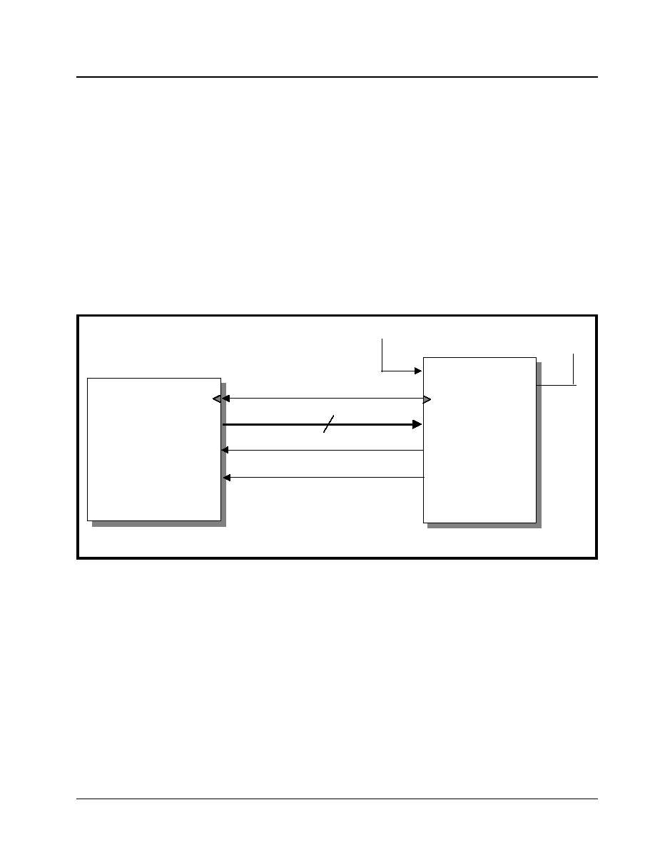
·Á
·Á
·Á
·Á
XRT7250
DS3/E3 FRAMER IC
REV. 1.1.1
351
The XRT7250 will accept the E3 payload data, from
the Terminal Equipment, in a parallel manner, via the
TxNib[3:0] input pins. The Transmit Terminal Equip-
ment Input Interface will latch this data into its circuit-
ry, on the rising edge of the TxNibClk output signal.
C. Delineation of Outbound E3 Frames
The Transmit Section will use the TxInClk input signal
as its timing reference and will initiate the generation
of E3 frames, asynchronous with respect to any ex-
ternal signal. The XRT7250 will pulse the TxFrame
output pin "High" whenever it is processing the last
bit, within a given Outbound E3 frame.
D. Sampling of payload data, from the Terminal
Equipment
In Mode 6, the XRT7250 will sample the data, at the
TxNib[3:0] input pins, on the third rising edge of the
TxInClk clock signal, following a pulse in the TxNibClk
signal (see Figure 168).
N
OTE
: The TxNibClk signal, from the XRT7250 operates
nominally at 8.592 MHz (e.g., 34.368 MHz divided by 4).
Interfacing the Transmit Payload Data Input Inter-
face block of the XRT7250 to the Terminal Equip-
ment for Mode 6 Operation
Figure 167 presents an illustration of the Transmit
Payload Data Input Interface block (within the
XRT7250) being interfaced to the Terminal Equip-
ment, for Mode 6 Operation.
Mode 6 Operation of the Terminal Equipment
In Figure 167 both the Terminal Equipment and the
XRT7250 will be driven by an external 8.592MHz
clock signal. The Teriminal Equipment will receive
the 8.592MHz clock signal via the E3_Nib_Clock_In
input pin. The XRT7250 will output the 8.592MHz
clock signal via the TxNibClk output pin.
The Terminal Equipment will serially output the data
on the E3_Data_Out[3:0] pins upon the rising edge of
the signal at the E3_Clock_In input pin. The
XRT7250 will latch the data, residing on the Tx-
Nib[3:0] input pins, on the rising edge of the TxNibClk
signal.
In this case the XRT7250 has the responsibility of
providing the framing reference signal by pulsing the
TxFrame output pin (and in turn the
Tx_Start_of_Frame input pin of the Terminal Equip-
ment) "High" for one bit-period, coincident with the
last bit within a given E3 frame.
Finally, the XRT7250 will always internally generate
the Overhead bits, when it is operating in both the E3
and Nibble-parallel modes. The XRT7250 will pull the
TxOHInd input pin "Low".
The behavior of the signals between the XRT7250
and the Terminal Equipment for E3 Mode 6 Operation
is illustrated in Figure 168.
F
IGURE
167. I
LLUSTRATION
OF
THE
T
ERMINAL
E
QUIPMENT
BEING
INTERFACED
TO
THE
T
RANSMIT
P
AYLOAD
D
ATA
I
NPUT
I
NTERFACE
BLOCK
OF
THE
XRT7250
FOR
M
ODE
6 O
PERATION
Terminal Equipment
XRT7250 E3 Framer
E3_Data_Out[3:0]
E3_Nib_Clock_In
Tx_Start_of_Frame
TxNib[3:0]
TxNibClk
TxNibFrame
NibInt
VCC
4
34.368MHz Clock Source
TxInClk
8.592MHz
TxOH_Ind
E3_Overhead_Ind
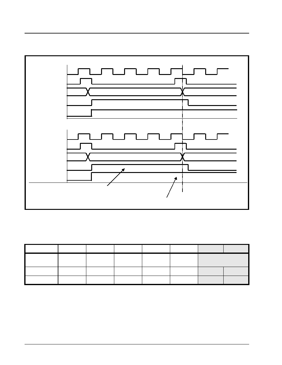
XRT7250
·Á
·Á
·Á
·Á
DS3/E3 FRAMER IC
REV. 1.1.1
352
How to configure the XRT7250 into Mode 6
1. Set the NibInt input pin "High".
2. Set the TimRefSel[1:0] bit-fields (within the
Framer Operating Mode Register) to "1X" as illus-
trated below.
3. Interface the XRT7250, to the Terminal Equip-
ment, as illustrated in Figure 167.
6.2.2
The Transmit Overhead Data Input Inter-
face
Figure 169 presents a simple illustration of the Trans-
mit Overhead Data Input Interface block within the
XRT7250.
F
IGURE
168. B
EHAVIOR
OF
THE
T
ERMINAL
I
NTERFACE
SIGNALS
BETWEEN
THE
XRT7250
AND
THE
T
ERMINAL
E
QUIPMENT
(E3 M
ODE
6 O
PERATION
)
Terminal Equipment Signals
TxInClk
Tx_Start_of_Frame
E3_Nib_Clock_In
E3_Data_Out[3:0]
Payload Nibble [1059]
Overhead Nibble [0]
XRT7250 Transmit Payload Data I/F Signals
E3 Frame Number N
E3 Frame Number N + 1
Note: TxNibFrame pulses high to denote
E3 Frame Boundary.
TxInClk
TxNibFrame
TxNibClk
TxNib[3:0]
Nibble [1059]
Overhead Nibble [0]
E3_Overhead_Ind
TxOH_Ind
TxOH_Ind pulses high for 4 Nibble periods
FRAMER OPERATING MODE REGISTER (ADDRESS = 0X00)
B
IT
7
B
IT
6
B
IT
5
B
IT
4
B
IT
3
B
IT
2
B
IT
1
B
IT
0
Local Loopback
DS3/E3*
Internal LOS
Enable
RESET
Interrupt
Enable Reset
Frame Format
TimRefSel[1:0]
R/W
R/W
R/W
R/W
R/W
R/W
R/W
R/W
0
0
1
0
1
0
1
x

·Á
·Á
·Á
·Á
XRT7250
DS3/E3 FRAMER IC
REV. 1.1.1
353
The E3, ITU-T G.832 Frame consists of 537 bytes.
Of these bytes, 530 bytes are payload bytes and the
remaining 7 are overhead bytes. The XRT7250 has
been designed to handle and process both the pay-
load type and overhead type bits for each E3 frame.
Within the Transmit Section within the XRT7250, the
Transmit Payload Data Input Interface has been de-
signed to handle the payload data. Likewise, the
Transmit Overhead Input Interface has been designed
to handle and process the overhead bits.
The Transmit Section of the XRT7250 generates or
processes the various overhead bits within the E3
frame, in the following manner.
The Frame Alignment Overhead Bytes (e.g., the
"FA1" and "FA2" bytes)
The "FA1" and "FA2" bytes are always internally gen-
erated by the Transmit Section of the XRT7250.
Hence, the user cannot insert his/her value for the
"FA1" and "FA2" bytes into the Outbound DS3 data
stream, via the Transmit Overhead Data Input Inter-
face.
The Error Monitoring (EM) Overhead Byte
The EM byte is always internally generated by the
Transmit Section of the XRT7250. Hence, the user
cannot insert his/her value for the EM byte into the
Outbound E3 data stream, via the Transmit Overhead
Data Input Interface.
The Alarm and signaling related Overhead bytes
Bytes that are used to transport the alarm conditions
can be either internally generated by the Transmit
Section within the XRT7250, or can be externally
generated and inserted into the Outbound E3 data
stream, via the Transmit Overhead Data Input Inter-
face. The E3 frame overhead bits that fall into this
category are:
∑ The "MA" byte
∑ The "TR" byte
The Data Link Related Overhead Bits
The E3 frame structure also contains bits which can
be used to transport User Data Link information and
Path Maintenance Data Link information. The UDL
(User Data Link) bits are only accessible via the
Transmit Overhead Data Input Interface. The Path
F
IGURE
169. S
IMPLE
I
LLUSTRATION
OF
THE
T
RANSMIT
O
VERHEAD
D
ATA
I
NPUT
I
NTERFACE
BLOCK
Transmit
Overhead
Data Input
Interface Block
Transmit
Overhead
Data Input
Interface Block
TxOHFrame
TxOHEnable
TxOH
TxOHClk
TxOHIns
To Transmit E3 Framer Block

XRT7250
·Á
·Á
·Á
·Á
DS3/E3 FRAMER IC
REV. 1.1.1
354
Maintenance Data Link (PMDL) bits can either be
sourced from the Transmit LAPD Controller/Buffer or
via the Transmit Overhead Data Input Interface.
Table 71 lists the Overhead Bits within the DS3 frame.
Additionally, this table also indicates whether or not
these overhead bits can be sourced by the Transmit
Overhead Data Input Interface or not.
T
ABLE
71: A L
ISTING
OF
THE
O
VERHEAD
BITS
WITHIN
THE
E3
FRAME
,
AND
THEIR
POTENTIAL
SOURCES
,
WITHIN
THE
XRT7250 IC
O
VERHEAD
B
IT
I
NTERNALLY
GENERATED
A
CCESSIBLE
VIA
THE
T
RANSMIT
O
VERHEAD
D
ATA
I
NPUT
I
NTERFACE
B
UFFER
/R
EGISTER
A
CCESSIBLE
FA1 - Bit 7
Yes
No
Yes*
FA1 - Bit 6
Yes
No
Yes
FA1 - Bit 5
Yes
No
Yes*
FA1 - Bit 4
Yes
No
Yes*
FA1 - Bit 3
Yes
No
Yes
FA1 - Bit 2
Yes
No
Yes
FA1 - Bit 1
Yes
No
Yes+
FA1 - Bit 0
Yes
No
Yes
FA2 - Bit 7
Yes
No
Yes
FA2 - Bit 6
Yes
No
Yes
FA2 - Bit 5
Yes
No
Yes
FA2 - Bit 4
Yes
No
Yes
FA2 - Bit 3
Yes
No
Yes
FA2 - Bit 2
Yes
No
Yes
FA2 - Bit 1
Yes
No
Yes
FA2 - Bit 0
Yes
No
Yes
EM - Bit 7
Yes
Yes
Yes
EM - Bit 6
Yes
Yes
Yes
EM - Bit 5
Yes
Yes
Yes
EM - Bit 4
Yes
Yes
Yes
EM - Bit 3
Yes
Yes
Yes
EM - Bit 2
Yes
Yes
Yes
EM - Bit 1
Yes
Yes
Yes
EM - Bit 0
Yes
Yes
Yes
TR - Bit 7
No
Yes
Yes
TR - Bit 6
No
Yes
Yes
TR - Bit 5
No
Yes
Yes
TR - Bit 4
No
Yes
Yes

·Á
·Á
·Á
·Á
XRT7250
DS3/E3 FRAMER IC
REV. 1.1.1
355
N
OTES
:
1. The XRT7250 contains mask register bits that per-
mit the user to alter the state of the internally gen-
erated value for these bits.
2. The Transmit LAPD Controller/Buffer can be config-
ured to be the source of the DL bits, within the Out-
bound E3 data stream.
In all, the Transmit Overhead Data Input Interface per-
mits the user to insert overhead data into the Out-
TR - Bit 3
No
Yes
Yes
TR - Bit 2
No
Yes
Yes
TR - Bit 1
No
Yes
Yes
TR - Bit 0
No
Yes
Yes
MA - Bit 7
Yes
Yes
Yes
MA - Bit 6
Yes
Yes
Yes
MA - Bit 5
Yes
Yes
Yes
MA - Bit 4
Yes
Yes
Yes
MA - Bit 3
Yes
Yes
Yes
MA - Bit 2
Yes
Yes
Yes
MA - Bit 1
Yes
Yes
Yes
MA - Bit 0
Yes
Yes
Yes
NR - Bit 7
No
Yes
Yes
NR - Bit 6
No
Yes
Yes
NR - Bit 5
No
Yes
Yes
NR - Bit 4
No
Yes
Yes
NR - Bit 3
No
Yes
Yes
NR - Bit 2
No
Yes
Yes
NR - Bit 1
No
Yes
Yes
NR - Bit 0
No
Yes
Yes
GC - Bit 7
No
Yes
Yes
GC - Bit 6
No
Yes
Yes
GC - Bit 5
No
Yes
Yes
GC - Bit 4
No
Yes
Yes
GC - Bit 3
No
Yes
Yes
GC - Bit 2
No
Yes
Yes
GC - Bit 1
No
Yes
Yes
GC - Bit 0
No
Yes
Yes
T
ABLE
71: A L
ISTING
OF
THE
O
VERHEAD
BITS
WITHIN
THE
E3
FRAME
,
AND
THEIR
POTENTIAL
SOURCES
,
WITHIN
THE
XRT7250 IC
O
VERHEAD
B
IT
I
NTERNALLY
GENERATED
A
CCESSIBLE
VIA
THE
T
RANSMIT
O
VERHEAD
D
ATA
I
NPUT
I
NTERFACE
B
UFFER
/R
EGISTER
A
CCESSIBLE

XRT7250
·Á
·Á
·Á
·Á
DS3/E3 FRAMER IC
REV. 1.1.1
356
bound E3 frames via the following two different meth-
ods.
∑ Method 1 - Using the TxOHClk clock signal
∑ Method 2 - Using the TxInClk and the TxOHEnable
signals.
Each of these methods are described below.
6.2.2.1
Method 1 - Using the TxOHClk Clock
Signal
The Transmit Overhead Data Input Interface consists
of the five signals. Of these five (5) signals, the fol-
lowing four (4) signals are to be used when imple-
menting Method 1.
∑ TxOH
∑ TxOHClk
∑ TxOHFrame
∑ TxOHIns
Each of these signals are listed and described below.
Table 72.
T
ABLE
72: D
ESCRIPTION
OF
M
ETHOD
1 T
RANSMIT
O
VERHEAD
I
NPUT
I
NTERFACE
S
IGNALS
N
AME
T
YPE
D
ESCRIPTION
TxOHIns
Input
Transmit Overhead Data Insert Enable input pin.
Asserting this input signal (e.g., setting it "High") enables the Transmit Overhead Data Input Inter-
face to accept overhead data from the Terminal Equipment. In other words, while this input pin is
"High", the Transmit Overhead Data Input Interface will sample the data at the TxOH input pin, on
the falling edge of the TxOHClk output signal.
Conversely, setting this pin "Low" configures the Transmit Overhead Data Input Interface to NOT
sample (e.g., ignore) the data at the TxOH input pin, on the falling edge of the TxOHClk output
signal.
N
OTE
: If the Terminal Equipment attempts to insert an overhead bit that cannot be accepted by
the Transmit Overhead Data Input Interface (e.g., if the Terminal Equipment asserts the TxOHIns
signal, at a time when one of these non-insertable overhead bits are being processed), that par-
ticular insertion effort will be ignored.
TxOH
Input
Transmit Overhead Data Input pin:
The Transmit Overhead Data Input Interface accepts the overhead data via this input
pin, and inserts into the overhead bit position within the very next Outbound E3 frame.
If the TxOHIns pin is pulled "High", the Transmit Overhead Data Input Interface will sam-
ple the data at this input pin (TxOH), on the falling edge of the TxOHClk output pin.
Conversely, if the TxOHIns pin is pulled "Low", then the Transmit Overhead Data Input
Interface will NOT sample the data at this input pin (TxOH). Consequently, this data will
be ignored.
TxOHClk
Output
Transmit Overhead Input Interface Clock Output signal:
This output signal serves two purposes:
1. The Transmit Overhead Data Input Interface will provide a rising clock edge on this signal, one
bit-period prior to the instant that the Transmit Overhead Data Input Interface is processing an
overhead bit.
2. The Transmit Overhead Data Input Interface will sample the data at the TxOH input, on the fall-
ing edge of this clock signal (provided that the TxOHIns input pin is "High").
N
OTE
: The Transmit Overhead Data Input Interface will supply a clock edge for all overhead bits
within the DS3 frame (via the TxOHClk output signal). This includes those overhead bits that the
Transmit Overhead Data Input Interface will not accept from the Terminal Equipment.
TxOHFrame
Output
Transmit Overhead Input Interface Frame Boundary Indicator Output:
This output signal pulses "High" when the XRT7250 is processing the last bit within a
given E3 frame.
The purpose of this output signal is to alert the Terminal Equipment that the Transmit
Overhead Data Input Interface block is about to begin processing the overhead bits for a
new E3 frame.
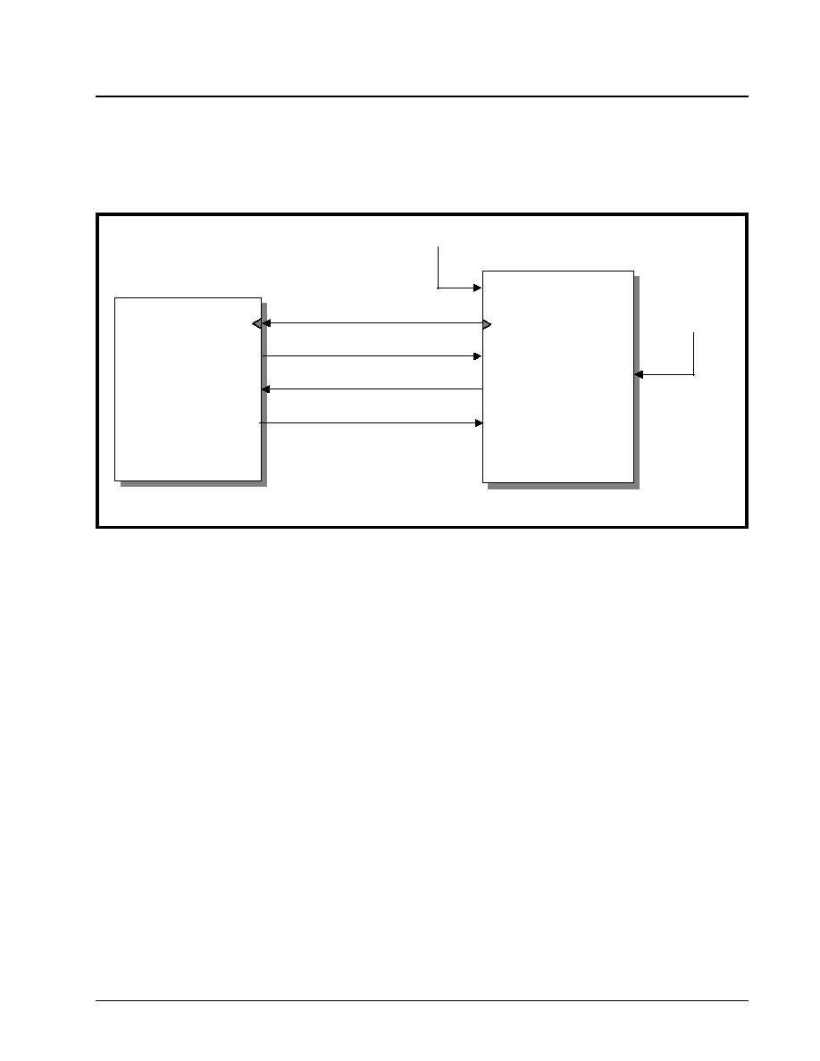
·Á
·Á
·Á
·Á
XRT7250
DS3/E3 FRAMER IC
REV. 1.1.1
357
Interfacing the Transmit Overhead Data Input In-
terface to the Terminal Equipment.
Figure 170 illustrates how one should interface the
Transmit Overhead Data Input Interface to the Termi-
nal Equipment, when using Method 1.
Method 1 Operation of the Terminal Equipment
If the Terminal Equipment intends to insert any over-
head data into the Outbound E3 data stream, (via the
Transmit Overhead Data Input Interface), then it is ex-
pected to do the following.
1. To sample the state of the TxOHFrame signal
(e.g., the Tx_Start_of_Frame input signal) on the
rising edge of the TxOHClk (e.g., the
E3_OH_Clock_In signal).
2. To keep track of the number of rising clock edges
that have occurred, via the TxOHClk (e.g., the
E3_OH_Clock_In signal) since the last time the
TxOHFrame signal was sampled "High". By
doing this the Terminal Equipment will be able to
keep track of which overhead bit is being pro-
cessed by the Transmit Overhead Data Input
Interface block at any given time. When the Ter-
minal Equipment knows which overhead bit is
being processed, at a given TxOHClk period, it
will know when to insert a desired overhead bit
value into the Outbound E3 data stream. From
this, the Terminal Equipment will know when it
should assert the TxOHIns input pin and place
the appropriate value on the TxOH input pin (of
the XRT7250).
Table 73 relates the number of rising clock edges (in
the TxOHClk signal, since TxOHFrame was sampled
"High") to the E3 Overhead Bit, that is being pro-
cessed.
F
IGURE
170. I
LLUSTRATION
OF
THE
T
ERMINAL
E
QUIPMENT
BEING
INTERFACED
TO
THE
T
RANSMIT
O
VERHEAD
D
ATA
I
NPUT
I
NTERFACE
(M
ETHOD
1)
Terminal Equipment
XRT7250 E3 Framer
E3_OH_Out]
E3_OH_Clock_In
Tx_Start_of_Frame
TxOHClk
TxOHFrame
TxOHIns
34.368 MHz Clock Source
TxInClk
TxOH
Insert_OH
RxLineClk
34.368 MHz
Clock Source

XRT7250
·Á
·Á
·Á
·Á
DS3/E3 FRAMER IC
REV. 1.1.1
358
T
ABLE
73: T
HE
R
ELATIONSHIP
BETWEEN
THE
N
UMBER
OF
R
ISING
C
LOCK
E
DGES
IN
T
X
OHC
LK
, (
SINCE
"T
X
OHF
RAME
"
WAS
LAST
SAMPLED
"H
IGH
")
TO
THE
E3 O
VERHEAD
B
IT
,
THAT
IS
BEING
PROCESSED
N
UMBER
OF
R
ISING
C
LOCK
E
DGES
IN
T
X
OHC
LK
T
HE
O
VERHEAD
B
IT
E
XPECTED
BY
THE
"XRT7250"
C
AN
THIS
OVERHEAD
BIT
BE
ACCEPTED
BY
THE
XRT7250?
0 (Clock edge is coincident with TxO-
HFrame being detected "High")
FA1 Byte - Bit 7
No
1
FA1 Byte - Bit 6
No
2
FA1 Byte - Bit 5
No
3
FA1 Byte - Bit 4
No
4
FA1 Byte - Bit 3
No
5
FA1 Byte - Bit 2
No
6
FA1 Byte - Bit 1
No
7
FA1 Byte - Bit 0
No
8
FA2 Byte - Bit 7
No
9
FA2 Byte - Bit 6
No
10
FA2 Byte - Bit 5
No
11
FA2 Byte - Bit 4
No
12
FA2 Byte - Bit 3
No
13
FA2 Byte - Bit 2
No
14
FA2 Byte - Bit 1
No
15
FA2 Byte - Bit 0
No
16
EM Byte - Bit 7
No
17
EM Byte - Bit 6
No
18
EM Byte - Bit 5
No
19
EM Byte - Bit 4
No
20
EM Byte - Bit 3
No
21
EM Byte - Bit 2
No
22
EM Byte - Bit 1
No
23
EM Byte - Bit 0
No
24
TR Byte - Bit 7
Yes
25
TR Byte - Bit 6
Yes
26
TR Byte - Bit 5
Yes
27
TR Byte - Bit 4
Yes
28
TR Byte - Bit 3
Yes
29
TR Byte - Bit 2
Yes

·Á
·Á
·Á
·Á
XRT7250
DS3/E3 FRAMER IC
REV. 1.1.1
359
3. After the Terminal Equipment has waited the
appropriate number of clock edges (from the
TxOHFrame signal being sampled "High"), it
should assert the TxOHIns input signal. Concur-
rently, the Terminal Equipment should also place
the appropriate value (of the inserted overhead
bit) onto the TxOH signal.
4. The Terminal Equipment should hold both the
TxOHIns input pin "High" and the value of the
TxOH signal, stable until the next rising edge of
TxOHClk is detected.
Case Study: The Terminal Equipment intends to
insert the appropriate overhead bits into the
Transmit Overhead Data Input Interface (using
30
TR Byte - Bit 1
Yes
31
TR Byte - Bit 0
Yes
32
MA Byte - Bit 7
Yes (FERF Bit)
33
MA Byte - Bit 6
Yes (FEBE Bit)
34
MA Byte - Bit 5
Yes
35
MA Byte - Bit 4
Yes
36
MA Byte - Bit 3
Yes
37
MA Byte - Bit 2
Yes
38
MA Byte - Bit 1
Yes
39
MA Byte - Bit 0
Yes
40
NR Byte - Bit 7
Yes
41
NR Byte - Bit 6
Yes
42
NR Byte - Bit 5
Yes
43
NR Byte - Bit 4
Yes
44
NR Byte - Bit 3
Yes
45
NR Byte - Bit 2
Yes
46
NR Byte - Bit 1
Yes
47
NR Byte - Bit 0
Yes
48
GC Byte - Bit 7
Yes
49
GC Byte - Bit 6
Yes
50
GC Byte - Bit 5
Yes
51
GC Byte - Bit 4
Yes
52
GC Byte - Bit 3
Yes
53
GC Byte - Bit 2
Yes
54
GC Byte - Bit 1
Yes
55
GC Byte - Bit 0
Yes
T
ABLE
73: T
HE
R
ELATIONSHIP
BETWEEN
THE
N
UMBER
OF
R
ISING
C
LOCK
E
DGES
IN
T
X
OHC
LK
, (
SINCE
"T
X
OHF
RAME
"
WAS
LAST
SAMPLED
"H
IGH
")
TO
THE
E3 O
VERHEAD
B
IT
,
THAT
IS
BEING
PROCESSED
N
UMBER
OF
R
ISING
C
LOCK
E
DGES
IN
T
X
OHC
LK
T
HE
O
VERHEAD
B
IT
E
XPECTED
BY
THE
"XRT7250"
C
AN
THIS
OVERHEAD
BIT
BE
ACCEPTED
BY
THE
XRT7250?
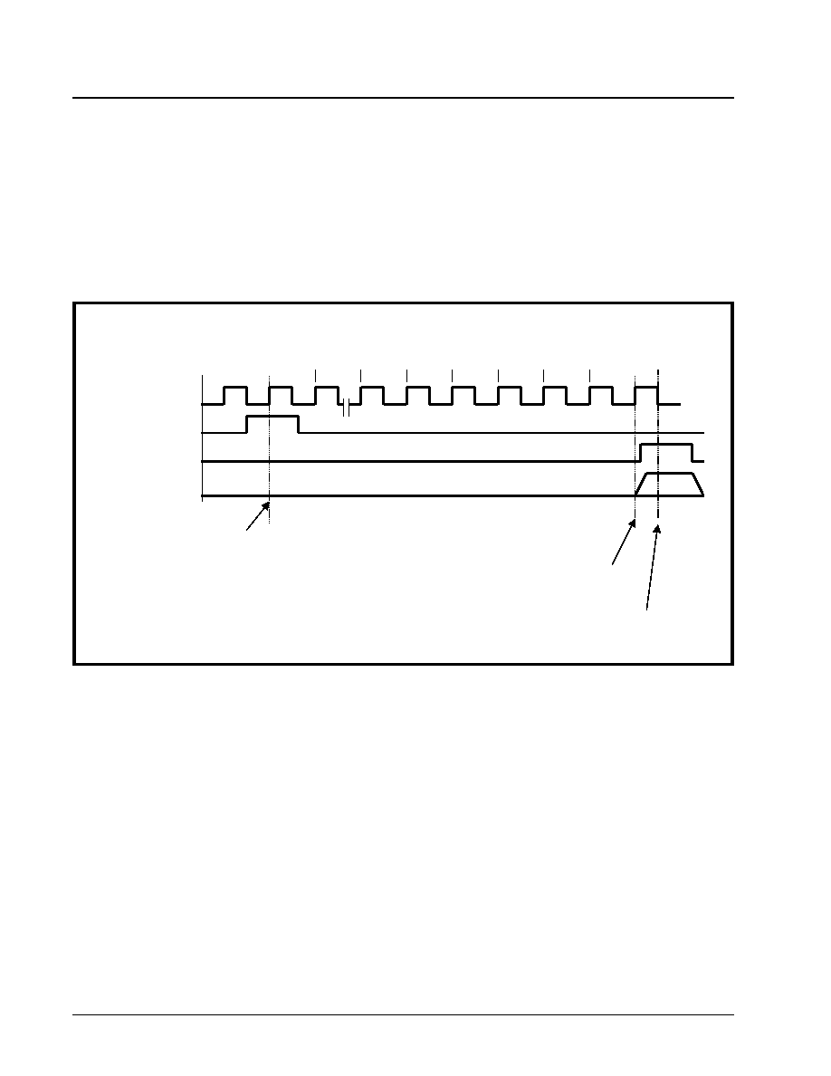
XRT7250
·Á
·Á
·Á
·Á
DS3/E3 FRAMER IC
REV. 1.1.1
360
Method 1) in order to transmit a Yellow Alarm to
the remote terminal equipment.
In this example, the Terminal Equipment intends to in-
sert the appropriate overhead bits, into the Transmit
Overhead Data Input Interface, such that the
XRT7250 will transmit a Yellow Alarm to the remote
terminal equipment. Recall that, for E3 Applications,
a Yellow Alarm is transmitted by setting the FERF bit
(within the MA Byte) to "0".
If one assumes that the connection between the Ter-
minal Equipment and the XRT7250 are as illustrated
in Figure 170 then Figure 171 presents an illustration
of the signaling that must go on between the Terminal
Equipment and the XRT7250.
In Figure 171 the Terminal Equipment samples the
TxOHFrame signal being "High" at rising clock edge #
"0". From this point, the Terminal Equipment waits
until it has detected 32 rising edges in the TxOHClk
signal. At this point, the Terminal Equipment knows
that the XRT7250 is just about to process the FERF
bit within the MA byte (in a given Outbound E3
frame). Additionally, according to Table 73, the 32nd
overhead bit to be processed is the FERF bit. In or-
der to facilitate the transmission of the Yellow Alarm,
the Terminal Equipment must set this FERF bit to "1".
Hence, the Terminal Equipment starts this process by
implementing the following steps concurrently.
a. Assert the TxOHIns input pin by setting it "High".
b. Set the TxOH input pin to "0".
After the Terminal Equipment has applied these sig-
nals, the XRT7250 will sample the data on both the
TxOHIns and TxOH signals upon the very next falling
edge of TxOHClk (designated at 32- in Figure 171).
Once the XRT7250 has sampled this data, it will then
insert a "1" into the FERF bit position, in the Out-
bound E3 frame.
Upon detection of the very next rising edge of the Tx-
OHClk clock signal (designated as clock edge 1 in
Figure 171), the Terminal Equipment will negate the
TxOHIns signal (e.g., toggles it "Low") and will cease
inserting data into the Transmit Overhead Data Input
Interface.
6.2.2.2
Method 2 - Using the TxInClk and
TxOHEnable Signals
Method 1 requires the use of an additional clock sig-
nal, TxOHClk. However, there may be a situation in
which the user does not wish to add this extra clock
signal to their design, in order to use the Transmit
Overhead Data Input Interface. Hence, Method 2 is
available. When using Method 2, either the TxInClk
or RxOutClk signal is used to sample the overhead
bits and signals which are input to the Transmit Over-
F
IGURE
171. I
LLUSTRATION
OF
THE
SIGNAL
THAT
MUST
OCCUR
BETWEEN
THE
T
ERMINAL
E
QUIPMENT
AND
THE
XRT7250,
IN
ORDER
TO
CONFIGURE
THE
XRT7250
TO
TRANSMIT
A
Y
ELLOW
A
LARM
TO
THE
REMOTE
TERMINAL
EQUIPMENT
Terminal Equipment/XRT7250 Interface Signals
TxOHClk
TxOHIns
TxOHFrame
TxOH
Remaining Overhead Bits with E3 Frame
MA, Bit 7
TxOHFrame is sample "high"
Terminal Equipment asserts TxOHIns and
Data on TxOH line.
0 1 26 27 28 29 30 31 32
XRT7250 Framer device samples TxOHIns and
TxOHIns signal

·Á
·Á
·Á
·Á
XRT7250
DS3/E3 FRAMER IC
REV. 1.1.1
361
head Data Input Interface. Method 2 involves the use
of the following signals:
∑ TxOH
∑ TxInClk
∑ TxOHFrame
∑ TxOHEnable
Each of these signals are listed and described in
Table 74.
Interfacing the Transmit Overhead Data Input Interface
to the Terminal Equipment
Figure 172 illustrates how one should interface the
Transmit Overhead Data Input Interface to the Termi-
nal Equipment when using Method 2.
T
ABLE
74: D
ESCRIPTION
OF
M
ETHOD
1 T
RANSMIT
O
VERHEAD
I
NPUT
I
NTERFACE
S
IGNALS
N
AME
T
YPE
D
ESCRIPTION
TxOHEnable
Output
Transmit Overhead Data Enable Output pin
The XRT7250 will assert this signal, for one TxInClk period, just prior to the instant that
the Transmit Overhead Data Input Interface is processing an overhead bit.
TxOHFrame
Output
Transmit Overhead Input Interface Frame Boundary Indicator Output:
This output signal pulses "High" when the XRT7250 is processing the last bit within a
given DS3 frame.
TxOHIns
Input
Transmit Overhead Data Insert Enable input pin.
Asserting this input signal (e.g., setting it "High") enables the Transmit Overhead Data Input Inter-
face to accept overhead data from the Terminal Equipment. In other words, while this input pin is
"High", the Transmit Overhead Data Input Interface will sample the data at the TxOH input pin, on
the falling edge of the TxInClk output signal.
Conversely, setting this pin "Low" configures the Transmit Overhead Data Input Interface to NOT
sample (e.g., ignore) the data at the TxOH input pin, on the falling edge of the TxOHClk output
signal.
N
OTE
: If the Terminal Equipment attempts to insert an overhead bit that cannot be accepted by
the Transmit Overhead Data Input Interface (e.g., if the Terminal Equipment asserts the TxOHIns
signal, at a time when one of these non-insertable overhead bits are being processed), that par-
ticular insertion effort will be ignored.
TxOH
Input
Transmit Overhead Data Input pin:
The Transmit Overhead Data Input Interface accepts the overhead data via this input
pin, and inserts into the overhead bit position within the very next Outbound DS3 frame.
If the TxOHIns pin is pulled "High", the Transmit Overhead Data Input Interface will sam-
ple the data at this input pin (TxOH), on the falling edge of the TxOHClk output pin.
Conversely, if the TxOHIns pin is pulled "Low", then the Transmit Overhead Data Input
Interface will NOT sample the data at this input pin (TxOH). Consequently, this data will
be ignored.
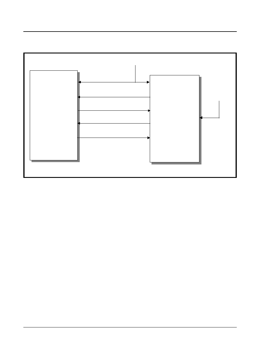
XRT7250
·Á
·Á
·Á
·Á
DS3/E3 FRAMER IC
REV. 1.1.1
362
Method 2 Operation of the Terminal Equipment
If the Terminal Equipment intends to insert any over-
head data into the Outbound E3 data stream (via the
Transmit Overhead Data Input Interface), then it is ex-
pected to do the following.
1. To sample the state of both the TxOHFrame and
the TxOHEnable input signals, via the
E3_Clock_In (e.g., either the TxInClk or the
RxOutClk signal of the XRT7250) signal. If the
Terminal Equipment samples the TxOHEnable
signal "High", then it knows that the XRT7250 is
about to process an overhead bit. Further, if the
Terminal Equipment samples both the TxO-
HFrame and the TxOHEnable pins "High" (at the
same time) then the Terminal Equipment knows
that the XRT7250 is about to process the first
overhead bit, within a new E3 frame.
2. To keep track of the number of times that the
TxOHEnable signal has been sampled "High"
since the last time both the TxOHFrame and the
TxOHEnable signals were sampled "High". By
doing this, the Terminal Equipment will be able to
keep track of which overhead bit the Transmit
Overhead Data Input Interface is about ready to
process. From this, the Terminal Equipment will
know when it should assert the TxOHIns input pin
and place the appropriate value on the TxOH
input pins of the XRT7250.
Table 75 also relates the number of TxOHEnable out-
put pulses (that have occurred since both the TxO-
HFrame and TxOHEnable pins were sampled "High")
to the E3 overhead bit, that is being processed.
F
IGURE
172. I
LLUSTRATION
OF
THE
T
ERMINAL
E
QUIPMENT
BEING
INTERFACED
TO
THE
T
RANSMIT
O
VERHEAD
D
ATA
I
NPUT
I
NTERFACE
(M
ETHOD
2)
Terminal Equipment
XRT7250 E3 Framer
E3_OH_Out
E3_OH_Enable
Tx_Start_of_Frame
TxOHEnable
TxOHFrame
TxOHIns
34.368 MHz Clock Source
TxInClk
TxOH
Insert_OH
RxLineClk
34.368 MHz
Clock Source
E3_Clock_In

·Á
·Á
·Á
·Á
XRT7250
DS3/E3 FRAMER IC
REV. 1.1.1
363
T
ABLE
75: T
HE
R
ELATIONSHIP
BETWEEN
THE
N
UMBER
OF
T
X
OHE
NABLE
PULSES
(
SINCE
THE
LAST
OCCURRENCE
OF
THE
T
X
OHF
RAME
PULSE
)
TO
THE
E3 O
VERHEAD
B
IT
,
THAT
IS
BEING
PROCESSED
BY
THE
XRT7250
N
UMBER
OF
T
X
OHE
NABLE
P
ULSES
T
HE
O
VERHEAD
B
IT
E
XPECTED
BY
THE
XRT7250
C
AN
THIS
OVERHEAD
BIT
BE
ACCEPTED
BY
THE
XRT7250?
0 (Clock edge is coincident with TxO-
HFrame being detected "High")
FA1 Byte - Bit 7
Yes
1
FA1 Byte - Bit 6
No
2
FA1 Byte - Bit 5
No
3
FA1 Byte - Bit 4
No
4
FA1 Byte - Bit 3
No
5
FA1 Byte - Bit 2
No
6
FA1 Byte - Bit 1
No
7
FA1 Byte - Bit 0
No
8
FA2 Byte - Bit 7
No
9
FA2 Byte - Bit 6
No
10
FA2 Byte - Bit 5
No
11
FA2 Byte - Bit 4
No
12
FA2 Byte - Bit 3
No
13
FA2 Byte - Bit 2
No
14
FA2 Byte - Bit 1
No
15
FA2 Byte - Bit 0
No
16
EM Byte - Bit 7
No
17
EM Byte - Bit 6
No
18
EM Byte - Bit 5
No
19
EM Byte - Bit 4
No
20
EM Byte - Bit 3
No
21
EM Byte - Bit 2
No
22
EM Byte - Bit 1
No
23
EM Byte - Bit 0
No
24
TR Byte - Bit 7
Yes
25
TR Byte - Bit 6
Yes
26
TR Byte - Bit 5
Yes
27
TR Byte - Bit 4
Yes
28
TR Byte - Bit 3
Yes
29
TR Byte - Bit 2
Yes

XRT7250
·Á
·Á
·Á
·Á
DS3/E3 FRAMER IC
REV. 1.1.1
364
3. After the Terminal Equipment has waited through
the appropriate number of pulses via the TxO-
HEnable pin, it should then assert the TxOHIns
input signal. Concurrently, the Terminal Equip-
ment should also place the appropriate value (of
the inserted overhead bit) onto the TxOH signal.
4. The Terminal Equipment should hold both the
TxOHIns input pin "High" and the value of the
TxOH signal stable, until the next TxOHEnable
pulse is detected.
Case Study: The Terminal Equipment intends to
insert the appropriate overhead bits into the
Transmit Overhead Data Input Interface (using
30
TR Byte - Bit 1
Yes
31
TR Byte - Bit 0
Yes
32
MA Byte - Bit 7 (FERF)
Yes
33
MA Byte - Bit 6 (FEBE)
Yes
34
MA Byte - Bit 5
Yes
35
MA Byte - Bit 4
Yes
36
MA Byte - Bit 3
Yes
37
MA Byte - Bit 2
Yes
38
MA Byte - Bit 1
Yes
39
MA Byte - Bit 0
Yes
40
NR Byte - Bit 7
Yes
41
NR Byte - Bit 6
Yes
42
NR Byte - Bit 5
Yes
43
NR Byte - Bit 4
Yes
44
NR Byte - Bit 3
Yes
45
NR Byte - Bit 2
Yes
46
NR Byte - Bit 1
Yes
47
NR Byte - Bit 0
Yes
48
GC Byte - Bit 7
Yes
49
GC Byte - Bit 6
Yes
50
GC Byte - Bit 5
Yes
51
GC Byte - Bit 4
Yes
52
GC Byte - Bit 3
Yes
53
GC Byte - Bit 2
Yes
54
GC Byte - Bit 1
Yes
55
GC Byte - Bit 0
Yes
T
ABLE
75: T
HE
R
ELATIONSHIP
BETWEEN
THE
N
UMBER
OF
T
X
OHE
NABLE
PULSES
(
SINCE
THE
LAST
OCCURRENCE
OF
THE
T
X
OHF
RAME
PULSE
)
TO
THE
E3 O
VERHEAD
B
IT
,
THAT
IS
BEING
PROCESSED
BY
THE
XRT7250
N
UMBER
OF
T
X
OHE
NABLE
P
ULSES
T
HE
O
VERHEAD
B
IT
E
XPECTED
BY
THE
XRT7250
C
AN
THIS
OVERHEAD
BIT
BE
ACCEPTED
BY
THE
XRT7250?

·Á
·Á
·Á
·Á
XRT7250
DS3/E3 FRAMER IC
REV. 1.1.1
365
Method 2) in order to transmit a Yellow Alarm to
the remote terminal equipment.
In this case, the Terminal Equipment intends to insert
the appropriate overhead bits, into the Transmit Over-
head Data Input Interface such that the XRT7250 will
transmit a Yellow Alarm to the remote terminal equip-
ment. Recall that, for E3, ITU-T G.832 applications, a
Yellow Alarm is transmitted by setting the FERF bit
(within the MA byte) to "1".
If one assumes that the connection between the Ter-
minal Equipment and the XRT7250 is as illustrated in
Figure 172 then, Figure 173 presents an illustration of
the signaling that must go on between the Terminal
Equipment and the XRT7250.
6.2.3
The Transmit E3 HDLC Controller
The Transmit E3 HDLC Controller block can be used
to transport Message-Oriented Signaling (MOS) type
messages to the remote terminal equipment as dis-
cussed in detail below.
N
OTE
: While executing this particular write operation, the
user should write the binary value "000xx110b" into the Tx
Controller block), please see Section 5.3.3.1.
6.2.3.1
Message-Oriented Signaling (e.g.,
LAP-D) processing via the Transmit DS3 HDLC
Controller
The LAPD Transmitter (within the Transmit E3 HDLC
Controller Block) allows the user to transmit path
maintenance data link (PMDL) messages to the re-
mote terminal via the Outbound E3 Frames. In this
case the message bits are either inserted into and
carried by the "NR" or the "GC" bytes, within the Out-
bound E3 frames. The on-chip LAPD transmitter sup-
ports both the 76 byte and 82 byte length message
formats, and the Framer IC allocates 88 bytes of on-
chip RAM (e.g., the Transmit LAPD Message buffer)
to store the message to be transmitted. The mes-
sage format complies with ITU-T Q.921 (LAP-D) pro-
tocol with different addresses and is presented below
in Figure 174.
F
IGURE
173. B
EHAVIOR
OF
T
RANSMIT
O
VERHEAD
D
ATA
I
NPUT
I
NTERFACE
SIGNALS
BETWEEN
THE
XRT7250
AND
THE
T
ERMINAL
E
QUIPMENT
(
FOR
M
ETHOD
2)
TxInClk
TxOHFrame
TxOHEnable
TxOHIns
TxOH
Terminal Equipment
samples "TxOHFrame" and
"TxOHEnable" being "HIGH"
Terminal Equipment counts the number of
TxOHEnable pulses. At "pulse # 32" the Terminal
Equipment asserts the "TxOHIns" signal and places the
desired data on TxOH.
XRT7250 samples TxOH
here.
TxOHEnable Pulse # 32
MA Byte, Bit 7
TxOHEnable Pulse # 0
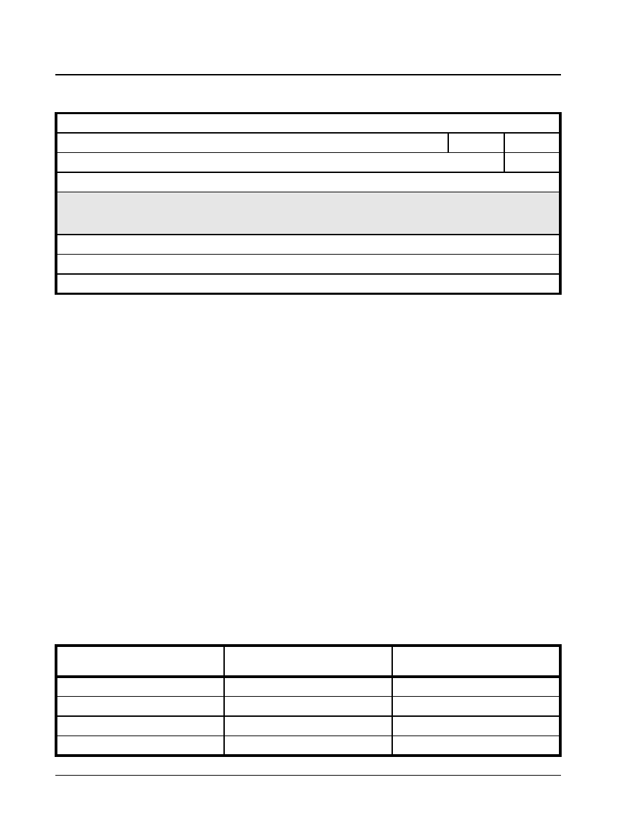
XRT7250
·Á
·Á
·Á
·Á
DS3/E3 FRAMER IC
REV. 1.1.1
366
Where: Flag Sequence = 0x7E
SAPI + CR + EA = 0x3C or 0x3E
TEI + EA = 0x01
Control = 0x03
The following sections defines each of these bit/byte-
fields within the LAPD Message Frame Format.
Flag Sequence Byte
The Flag Sequence byte is of the value 0x7E, and is
used to denote the boundaries of the LAPD Message
Frame.
SAPI - Service Access Point Identifier
The SAPI bit-fields are assigned the value of
"001111b" or 15 (decimal).
TEI - Terminal Endpoint Identifier
The TEI bit-fields are assigned the value of 0x00.
The TEI field is used in N-ISDN systems to identify a
terminal out of multiple possible terminal. However,
since the Framer IC transmits data in a point-to-point
manner, the TEI value is unimportant.
Control
The Control identifies the type of frame being trans-
mitted. There are three general types of frame for-
mats: Information, Supervisory, and Unnumbered.
The Framer assigned the Control byte the value 03h.
Hence, the Framer will be transmitting and receiving
Unnumbered LAPD Message frames.
Information Payload
The Information Payload is the 76 bytes or 82 bytes of
data (e.g., the PMDL Message) that the user has writ-
ten into the on-chip Transmit LAPD Message buffer
(which is located at addresses 0x86 through 0xDD).
It is important to note that the user must write in a
specific octet value into the first byte position within
the Transmit LAPD Message buffer (located at Ad-
dress = 0x86, within the Framer). The value of this
octet depends upon the type of LAPD Message
frame/PMDL Message that the user wishes to trans-
mit. Table 76 presents a list of the various types of
LAPD Message frames/PMDL Messages that are
supported by the XRT7250 Framer device and the
corresponding octet value that the user must write in-
to the first octet position within the Transmit LAPD
Message buffer.
F
IGURE
174. LAPD M
ESSAGE
F
RAME
F
ORMAT
Flag Sequence (8 bits)
SAPI (6-bits)
C/R
EA
TEI (7 bits)
EA
Control (8-bits)
76 or 82 Bytes of Information (Payload)
FCS - MSB
FCS - LSB
Flag Sequence (8-bits)
T
ABLE
76: T
HE
LAPD M
ESSAGE
T
YPE
AND
THE
C
ORRESPONDING
VALUE
OF
THE
F
IRST
B
YTE
,
WITHIN
THE
I
NFORMATION
P
AYLOAD
LAPD M
ESSAGE
T
YPE
V
ALUE
OF
F
IRST
B
YTE
,
WITHIN
I
NFORMATION
P
AYLOAD
OF
M
ESSAGE
M
ESSAGE
S
IZE
CL Path Identification
0x38
76 bytes
IDLE Signal Identification
0x34
76 bytes
Test Signal Identification
0x32
76 bytes
ITU-T Path Identification
0x3F
82 bytes
·Á
·Á
·Á
·Á
XRT7250
DS3/E3 FRAMER IC
REV. 1.1.1
367
Frame Check Sequence Bytes
The 16 bit FCS (Frame Check Sequence) is calculat-
ed over the LAPD Message Header and Information
Payload bytes, by using the CRC-16 polynomial, x
16
+ x
12
+ x
5
+ 1.
Operation of the LAPD Transmitter
If a message is to be transmitted via the LAPD Trans-
mitter then, the information portion (or the body) of
the message must be written into the Transmit LAPD
Message Buffer, which is located at 0x86 through
0xDD in on-chip RAM via the Microprocessor Inter-
face. Afterwards, the user must do three things:
1. Specify the length of LAPD message to be trans-
mitted.
2. Specify which bit-field (within the E3 frame) that
the LAPD Message frame is to be transported on
(e.g., either the "GC" or the "NR" byte).
3. Specify whether the LAPD Transmitter should
transmit this LAPD Message frame only once, or
an indefinite number of times at One-Second
intervals.
4. Enable the LAPD Transmitter.
5. Initiate the Transmission of the PMDL Message.
Each of these steps will be discussed in detail.
STEP 1 - Specify the type of LAPD Message frame
to be Transmitted (within the Transmit LAPD Mes-
sage Buffer)
The user must write in a specific octet value into the
first octet position within the Transmit LAPD Buffer
(e.g., at Address Location 0x86 within the Framer IC).
This octet is referred to as the LAPD Message Frame
ID octet. The value of this octet must correspond to
the type of LAPD Message frame that is to be trans-
mitted. This octet will ultimately be used by the Re-
mote Terminal Equipment in order to help it identify
the type of LAPD message frame that it is receiving.
Table 76 lists these octets and the corresponding
LAPD Message types.
STEP 2 - Write the PMDL Message into the re-
maining part of the Transmit LAPD Message Buff-
er.
The user must now write in his/her PMDL Message
into the remaining portion of the Transmit LAPD Mes-
sage buffer (e.g., addresses 0x87 through 0x135
within the Framer IC).
STEP 3 - Specifying the Length of the LAPD Mes-
sage
One of two different sizes of LAPD Messages can be
transmitted, by writing the appropriate data to bit 1
within the Tx E3 LAPD Configuration Register. The
bit-format of this register is presented below.
The relationship between the contents of bit-fields 1
and the LAPD Message size is given in Table 77.
N
OTE
: The Message Type selected must correspond with
the contents of the first byte of the Information (Payload)
portion, as presented in Table 76.
STEP 4 - Specifying which byte-field (within the
E3 frame) that the LAPD Message frame octets
are to be transported on.
The Transmit E3 Framer block allows the user to
transport the LAPD Message frame octets via either
the "NR" byte or the "GC" byte-field, within each Out-
bound E3 frame. The user makes this selection by
writing the appropriate value to bit-field 4 (DLinNR),
TRANSMIT E3 LAPD CONFIGURATION REGISTER (ADDRESS = 0X33)
B
IT
7
B
IT
6
B
IT
5
B
IT
4
B
IT
3
B
IT
2
B
IT
1
B
IT
0
Not Used
Auto
Retransmit
Not Used
TxLAPD
Msg Length
TxLAPD
Enable
R/O
R/O
R/O
R/O
R/W
R/O
R/W
R/W
0
0
0
0
X
0
X
X
T
ABLE
77: R
ELATIONSHIP
BETWEEN
T
X
LAPD M
SG
L
ENGTH
AND
THE
LAPD M
ESSAGE
S
IZE
T
X
LAPD M
ESSAGE
L
ENGTH
LAPD M
ESSAGE
L
ENGTH
0
LAPD Message size is 76 bytes
1
LAPD Message size is 82 bytes
XRT7250
·Á
·Á
·Á
·Á
DS3/E3 FRAMER IC
REV. 1.1.1
368
within the Tx E3 Configuration Register, as depicted
below.
)
If the user writes a "0" into this bit-field, then the
LAPD Transmitter will transmit the comprising octets
of the Outbound LAPD Message frame via the GC
byte field. Additionally, the Transmit E3 Framer block
will insert the contents of the TxNR Byte Register
(Address = 0x37) into the "NR" byte of each Out-
bound E3 frame.
Conversely, if the user writes a "1" into this bit-field,
then the LAPD Transmitter will transmit the Outbound
LAPD Message frame octets via the NR byte-field,
within each Outbound E3 frame. Additionally, the
Transmit E3 Framer will insert the contents of the Tx
GC Byte Register (Address = 0x35) into the GC byte-
field of each Outbound E3 frame.
STEP 5 - Specify whether the LAPD Transmitter
should transmit the LAPD Message frame only
once, or an indefinite number of times at One-
Second intervals.
The Transmit E3 HDLC Control block allows the user
to configure the LAPD Transmitter to transmit this
LAPD Message frame only once, or an indefinite
number of times at One-Second intervals. The user
implements this configuration by writing the appropri-
ate value into Bit 3 (Auto Retransmit) within the Tx E3
LAPD Configuration Register (Address = 0x33), as
depicted below.
)
If the user writes a "1" into this bit-field, then the
LAPD Transmitter will transmit the LAPD Message
frame repeatedly at One-Second intervals until the
LAPD Transmitter is disabled.
If the user writes a "0" into this bit-field, then the
LAPD Transmitter will transmit the LAPD Message
frame only once. Afterwards, the LAPD Transmitter
will halt its transmission until the user invokes the
Transmit LAPD Message frame command, once
again.
STEP 6 - Enabling the LAPD Transmitter
Prior to the transmission of any data via the LAPD
Transmitter, the LAPD Transmitter must be enabled
by writing a "1" to bit 0 (TxLAPD Enable) of the Tx E3
LAPD Configuration Register, as depicted below.
TXE3 CONFIGURATION REGISTER (ADDRESS = 0X30)
B
IT
7
B
IT
6
B
IT
5
B
IT
4
B
IT
3
B
IT
2
B
IT
1
B
IT
0
Not Used
TxDL
in NR
Not Used
TxAIS
Enable
TxLOS
Enable
TxMARx
RO
RO
RO
R/W
RO
R/W
R/W
R/W
0
0
0
0
0
0
0
0
TXE3 LAPD CONFIGURATION REGISTER (ADDRESS = 0X33)
B
IT
7
B
IT
6
B
IT
5
B
IT
4
B
IT
3
B
IT
2
B
IT
1
B
IT
0
Not Used
Auto
Retransmit
Not Used
TxLAPD
Msg Length
TxLAPD
Enable
RO
RO
RO
RO
R/W
RO
R/W
R/W
0
0
0
0
1
0
0
0
TRANSMIT E3 LAPD CONFIGURATION REGISTER (ADDRESS = 0X33)
B
IT
7
B
IT
6
B
IT
5
B
IT
4
B
IT
3
B
IT
2
B
IT
1
B
IT
0
Not Used
Auto
Retransmit
Not Used
TxLAPD
Msg Length
TxLAPD
Enable
R/O
R/O
R/O
R/O
R/W
R/O
R/W
R/W
0
0
0
0
X
0
X
X

·Á
·Á
·Á
·Á
XRT7250
DS3/E3 FRAMER IC
REV. 1.1.1
369
If the user writes a "0" into this bit-field, then the
LAPD Transmitter will be enabled, and the LAPD
Transmitter will immediately begin to transmit a con-
tinuous stream of Flag Sequence octets (0x7E), via
either the "GC" or the "NR" byte-field of each Out-
bound E3 frame (depending upon which byte has
been selected to carry the PMDL channel).
Conversely, if the user writes a "1" into this bit-field,
then the LAPD Transmitter will be disabled. The
Transmit E3 Framer block will insert the contents of
the Tx GC Byte Register into the "GC" byte-field for
each Outbound E3 frame. Likewise, the Transmit E3
Framer block will also insert the contents of the Tx
NR Byte Register into the NR" byte-field for each Out-
bound E3 frame. No transmission of PMDL data will
occur.
STEP 7 - Initiate the Transmission
At this point, the user should have written the PMDL
message into the on-chip Transmit LAPD Message
buffer and should have specified the type of LAPD
Message that is to be transmitted. The user should
have also specified whether the LAPD Transmitter will
transport the LAPD Message frame octets via the
GC-byte field or via the NR-byte field of each Out-
bound E3 frame. Finally the LAPD Transmitter should
have been enabled. Then initiate the transmission of
this message by writing a "1" to Bit 3 (Tx DL Start)
within the Tx E3 LAPD Status and Interrupt Register
(Address = 0x34), as depicted below.
)
A "0" to "1" transition in Bit 3 (TxDL Start) in this regis-
ter, initiates the transmission of LAPD Message
frames. At this point, the LAPD Transmitter will begin
to search thorugh the PMDL message, which is resid-
ing within the Transmit LAPD Message buffer. If the
LAPD Transmitter finds any string of five (5) consecu-
tive "1's" in the PMDL Message, then the LAPD
Transmitter will insert a "0" immediately following
these strings of consecutive "1's". This procedure is
known as stuffing. The purpose of PMDL Message
stuffing is to insure that the user's PMDL Message
does not contain strings of data that mimic the Flag
Sequence octet (e.g., six consecutive "1's") or the
ABORT Sequence octet (e.g., seven consecutive
"1's"). Afterwards, the LAPD Transmitter will begin to
encapsulate the PMDL Message, residing in the
Transmit LAPD Message buffer, into a LAPD Mes-
sage frame. Finally, the LAPD Transmitter will frag-
ment the Outbound LAPD Message frame into octets
and will begin to transport these octets via the GC or
the NR byte-fields (depending upon the user's selec-
tion) of each Outbound E3 frame.
While the LAPD Transmitter is transmitting this LAPD
Message frame, the TxDL Busy bit-field (Bit 2) within
the Tx E3 LAPD Status and Interrupt Register, will be
set to "1". This bit-field allows the user to poll the sta-
tus of the LAPD Transmitter. Once the LAPD Trans-
mitter has completed the transmission of the LAPD
Message, then this bit-field will toggle back to "0".
The user can configure the LAPD Transmitter to inter-
rupt the local Microprocessor/Microcontroller upon
completion of transmission of the LAPD Message
frame, by setting bit-field 1 (TxLAPD Interrupt Enable)
within the Tx E3 LAPD Status and Interrupt register
(Address = 0x34). to "1" as depicted below.
TXE3 LAPD STATUS AND INTERRUPT REGISTER (ADDRESS = 0X34)
B
IT
7
B
IT
6
B
IT
5
B
IT
4
B
IT
3
B
IT
2
B
IT
1
B
IT
0
Not Used
TxDL Start
TxDL Busy
TxLAPD
Interrupt
Enable
TxLAPD
Interrupt
Status
RO
RO
RO
RO
R/W
RO
R/W
RUR
0
0
0
0
0
0
0
0

XRT7250
·Á
·Á
·Á
·Á
DS3/E3 FRAMER IC
REV. 1.1.1
370
`The purpose of t his interrupt is to let the Micropro-
cessor/Microcontroller know that the LAPD Transmit-
ter is available and ready to transmit a LAPD Mes-
sage frame (which contains a new PMDL Message)
to the remote terminal equipment. Bit 0 (Tx LAPD In-
terrupt Status) within the Tx E3 LAPD Status and In-
terrupt Register will reflect the status for the Transmit
LAPD Interrupt.
N
OTE
: This bit-field will be reset upon reading this register.
Summary of Operating the LAPD Transmitter
Once the user has invoked the TxDL Start command,
the LAPD Transmitter will do the following.
∑ Generate the four octets of the LAPD Message
frame header (e.g., the Flag Sequence, SAPI, TEI,
Control, etc.,) and insert them into the header byte
positions within the LAPD Message frame.
∑ It will read in the contents of the Transmit LAPD
Message buffer (e.g., the PMDL Message data)
and insert it into the Information Payload portion of
the LAPD Message frame.
∑ Compute the 16-bit Frame Check Sequence (FCS)
value of the LAPD Message frame (e.g, of the
LAPD Message header and Payload bytes) and
insert this value into the FCS value octet positions
within the LAPD Message frame.
∑ Append a trailer Flag Sequence octet to the end of
the LAPD Message frame (following the 16-bit FCS
octets).
∑ Fragment the resulting LAPD Message frame into
octets and begin inserting these octets into either
the GC or NR byte-fields within the Outbound E3
frames (depending upon the user's selection).
∑ Complete the transmission of the overhead bytes,
information payload byte, FCS value, and the trail-
ing Flag Sequence octets via the Transmit E3
Framer block.
Once the LAPD Transmitter has completed its trans-
mission of the LAPD Message frame, the Framer will
generate an Interrupt to the MIcroprocessor/Micro-
controller (if enabled). Afterwards, the LAPD Trans-
mitter will either halt its transmission of LAPD Mes-
sage frames or will proceed to retransmit the LAPD
Message frame, repeatedly at One-Second inter-
vals. In between these transmissions of the LAPD
Message frames, the LAPD Transmitter will be send-
ing a continuous stream of Flag Sequence bytes.
The LAPD Transmitter will continue this behavior until
the user has disabled the LAPD Transmitter by writing
a "1" into bit 3 (No Data Link) within the Tx E3 Config-
uration register.
N
OTE
: In order to prevent the user's data (e.g., the PMDL
Message within the LAPD Message frame) from mimicking
the Flag Sequence byte or an ABORT Sequence, the LAPD
Transmitter will parse through the PMDL Message data and
insert a "0" into this data, immediately following the detec-
tion of five (5) consecutive "1's" (this stuffing occurs while
the PMDL message data is being read in from the Transmit
LAPD Message frame. The Remote LAPD Receive (See
Section 5.3.5) will have the responsibility of checking the
newly received PMDL messages for a string of five (5) con-
secutive "1's" and removing the subsequent "0" from the
payload portion of the incoming LAPD Message.
Figure 175 is a flow chart that depicts the procedure
(in white boxes) that the user should use in order to
transmit a PMDL message via the LAPD Transmitter,
when the LAPD Transmitter is configured to retrans-
mit the LAPD Message frame, repeatedly at One-
Second intervals. This figure also indicates (via the
Shaded boxes) what the LAPD Transmitter circuitry
will do before and during message transmission.
TXE3 LAPD STATUS AND INTERRUPT REGISTER (ADDRESS = 0X34)
B
IT
7
B
IT
6
B
IT
5
B
IT
4
B
IT
3
B
IT
2
B
IT
1
B
IT
0
Not Used
TxDL Start
TxDL Busy
TxLAPD
Interrupt
Enable
TxLAPD
Interrupt
Status
RO
RO
RO
RO
R/W
RO
R/W
RUR
0
0
0
0
0
0
0
0
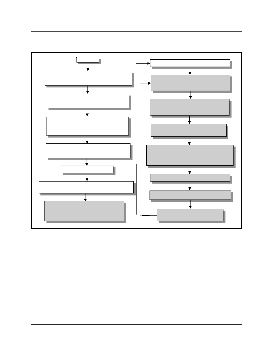
·Á
·Á
·Á
·Á
XRT7250
DS3/E3 FRAMER IC
REV. 1.1.1
371
Figure 176 presents the procedure (in white boxes)
which the user should use in order to transmit a PM-
DL Message via the LAPD Transmitter, when the
LAPD Transmitter is configured to transmit a LAPD
Message frame only once, and then halt transmis-
sion.
F
IGURE
175. F
LOW
C
HART
DEPICTING
HOW
TO
USE
THE
LAPD T
RANSMITTER
(LAPD T
RANSMITTER
IS
CONFIGURED
TO
RE
-
TRANSMIT
THE
LAPD M
ESSAGE
FRAME
REPEATEDLY
AT
O
NE
-S
ECOND
INTERVALS
)
Start
Write the "LAPD Message frame identification"
octet into the first octet position within the
"Transmit LAPD Message" buffer (Address = 0x86).
Write the PMDL Message into the remaining
portion of the "Transmit LAPD Message" buffer
(from 0x87 to 0xDD).
Specify the type/size of the LAPD Message frame
to be transmitted.
Write in the appropriate value into bits 5 and 6
within the Tx E3 LAPD Configuration Register
Enable the LAPD Transmitter
Initiate the LAPD Message frame transmission.
Specify whether the "outbound" LAPD Message
frame is to be transported via the GC or the NR
byte-fields, within each "outbound" E3 Frame
LAPD Transmitter will generate a continuous
string of "Flag Sequence" bytes. These bytes will
be transported via either the GC or the NR byte
field (depending upon user's selection).
LAPD Transmitter will "stuff" the contents of the
PMDL Message (residing within the "Transmit
LAPD Message" buffer).
LAPD Transmitter will read out "stuff" PMDL
Message and encapsulate it into a LAPD Message
frame.
LAPD Transmitter will compute and insert the
FCS value, into the LAPD Message frame.
LAPD Transmitter will fragment LAPD Message
frame into "octets" and begin to insert these octets into
the GC or NR byte-field (depending upon user's
selection) into each "outbound" E3 frame.
Complete transmission of LAPD Message frame.
Generate "Completion of Transmission of LAPD
Message frame Interrupt.
Wait One Second. Generate a continuous
string of Flag Sequence Bytes
Configure the LAPD Transmitter to repeat transmissions
of the LAPD Message frame at one-second intervals.

XRT7250
·Á
·Á
·Á
·Á
DS3/E3 FRAMER IC
REV. 1.1.1
372
The Mechanics of Transmitting a New LAPD Mes-
sage frame, if the LAPD Transmitter has been
configured to re-transmit the LAPD Message
frame, repeatedly, at One-Second intervals.
If the LAPD Transmitter has been configured to re-
transmit the LAPD Message frame repeatedly at
One-Second intervals, then it will do the following (at
One-Second intervals).
∑ Stuff the PMDL Message.
∑ Read in the stuffed PMDL Message from the Trans-
mit LAPD Message buffer.
∑ Encapsulate this stuffed PMDL Message into a
LAPD Message frame.
∑ Transmit this LAPD Message frame to the Remote
Terminal Equipment.
If another (e.g., a different) PMDL Message is to be
transmitted to the Remote Terminal Equipment this
new message will have to be written into the Transmit
LAPD Message buffer, via the Microprocessor Inter-
face block of the Framer IC. However, care must be
taken when writing this new PMDL message. If this
message is written into the Transmit LAPD Message
buffer at the wrong time (with respect to these One-
Second LAPD Message frame transmissions), the
user's action could interfere with these transmissions,
thereby causing the LAPD Transmitter to transmit a
corrupted message to the Remote Terminal Equip-
F
IGURE
176. F
LOW
C
HART
DEPICTING
HOW
TO
USE
THE
LAPD T
RANSMITTER
(LAPD T
RANSMITTER
IS
CONFIGURED
TO
TRANSMIT
A
LAPD M
ESSAGE
FRAME
ONLY
ONCE
).
Start
Write the "LAPD Message frame identification"
octet into the first octet position within the
"Transmit LAPD Message" buffer (Address = 0x86).
Write the PMDL Message into the remaining
portion of the "Transmit LAPD Message" buffer
(from 0x87 to 0xDD).
Specify the type/size of the LAPD Message frame
to be transmitted.
Write in the appropriate value into bits 5 and 6
within the Tx E3 LAPD Configuration Register
Enable the LAPD Transmitter
Initiate the LAPD Message frame transmission.
Specify whether the "outbound" LAPD Message
frame is to be transported via the GC or the NR
byte-fields, within each "outbound" E3 Frame
LAPD Transmitter will generate a continuous
string of "Flag Sequence" bytes. These bytes will
be transported via either the GC or the NR byte
field (depending upon user's selection).
LAPD Transmitter will "stuff" the contents of the
PMDL Message (residing within the "Transmit
LAPD Message" buffer).
LAPD Transmitter will read out "stuff" PMDL Message
and encapsulate it into a LAPD Message frame.
LAPD Transmitter will compute and insert the
FCS value, into the LAPD Message frame.
LAPD Transmitter will fragment LAPD Message
frame into "octets" and begin to insert these octets into
the GC or NR byte-field (depending upon user's
selection) into each "outbound" E3 frame.
Complete transmission of LAPD Message frame.
Generate "Completion of Transmission of LAPD
Message frame Interrupt.
Halt Transmission for an "indefinite period.
Wait until the user initiates "LAPD Message
Frame Transmission" again.
Configure the LAPD Transmitter to transmit
LAPD Message Frame Only Once

·Á
·Á
·Á
·Á
XRT7250
DS3/E3 FRAMER IC
REV. 1.1.1
373
ment. In order to avoid this problem, while writing the
new message into the Transmit LAPD Message buff-
er, the user should do the following.
1. Configure the Framer to automatically reset acti-
vated interrupts.
The user can do this by writing a "1" into Bit 3 within
the Framer Operating Mode register (Address =
0x00), as depicted below.
This action will prevent the LAPD Transmitter from
generating its own One-Second interrupt (following
each transmission of the LAPD Message frame).
2. Enable the One-Second Interrupt
This can be done by writing a "1" into Bit 0 (One-Sec-
ond Interrupt Enable) within the Block Interrupt En-
able Register, as depicted below.
3. Write the new message into the Transmit LAPD
Message buffer immediately after the occurrence
of the One-Second Interrupt
By synchronizing the writes to the Transmit LAPD
Message buffer to occur immediately after the occur-
rence of the One-Second Interrupt, the user avoids
conflicting with the One-Second transmission of the
LAPD Message frame, and will transmit the correct
(uncorrupted) PMDL Message to the Remote LAPD
Receiver.
6.2.4
The Transmit E3 Framer Block
6.2.4.1
Brief Description of the Transmit E3
Framer
The Transmit E3 Framer block accepts data from any
of the following three sources, and uses it to form the
E3 data stream.
∑ The Transmit Payload Data Input block
∑ The Transmit Overhead Data Input block
∑ The Transmit HDLC Controller block
∑ The Internal Overhead Data Generator
The manner in how the Transmit E3 Framer block
handles data from each of these sources is described
below.
Handling of data from the Transmit Payload Data
Input Interface
For E3 applications, all data that is input to the Trans-
mit Payload Data Input Interface will be inserted into
the payload bit positions within the Outbound E3
frames.
Handling of data from the Internal Overhead Bit
Generator
By default, the Transmit E3 Framer block will internal-
ly generate the overhead bytes. However, if the Ter-
minal Equipment inserts its own values for the over-
head bits or bytes (via the Transmit Overhead Data
Input Interface) or, if the user enables and employs
the Transmit E3 HDLC Controller block, then these in-
ternally generated overhead bytes will be overwritten.
Handling of data from the Transmit Overhead Da-
ta Input Interface
FRAMER OPERATING MODE REGISTER (ADDRESS = 0X00)
B
IT
7
B
IT
6
B
IT
5
B
IT
4
B
IT
3
B
IT
2
B
IT
1
B
IT
0
Local Loopback
DS3/E3*
Internal
LOS
Enable
RESET
Interrupt
Enable Reset
Frame Format
TimRefSel[1:0]
R/W
R/W
R/W
R/W
R/W
R/W
R/W
R/W
0
0
1
0
1
0
1
1
BLOCK INTERRUPT ENABLE REGISTER (ADDRESS = 0X04)
B
IT
7
B
IT
6
B
IT
5
B
IT
4
B
IT
3
B
IT
2
B
IT
1
B
IT
0
RxDS3/E3
Interrupt
Enable
Not Used
TxDS3/E3
Interrupt
Enable
One-Second
Interrupt
Enable
R/W
RO
RO
RO
RO
RO
R/W
R/W
0
0
0
0
0
0
0
0
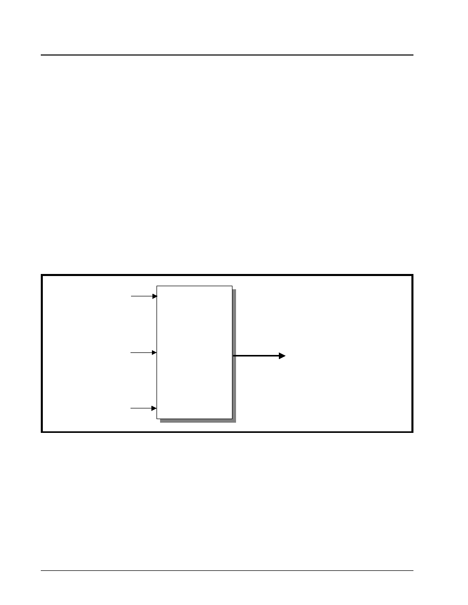
XRT7250
·Á
·Á
·Á
·Á
DS3/E3 FRAMER IC
REV. 1.1.1
374
For E3 applications, the Transmit E3 Framer block au-
tomatically generates and inserts the framing align-
ment bytes (e.g., the "FA1" and "FA2" framing align-
ment bytes) into the Outbound E3 frames. Further,
the Transmit E3 Framer block will automatically com-
pute and insert the EM byte into the Outbound E3
frames. Hence, the Transmit E3 Framer block will not
accept data from the Transmit OH Data Input Inter-
face block for the "FA1", "FA2" and "EM" bytes.
However, the Transmit E3 Framer block will accept
(and insert) data from the Transmit Overhead Data In-
put Interface for the following byte-fields.
∑ MA byte
∑ TR byte
∑ NR byte
∑ GC byte
If the user's local Data Link Equipment activates the
Transmit Overhead Data Input Interface block and
writes data into this interface for these bits or bytes,
then the Transmit E3 Framer block will insert this data
into the appropriate overhead bit/byte-fields, within
the Outbound E3 frames.
6.2.4.2
Detailed Functional Description of the
Transmit E3 Framer Block
The Transmit E3 Framer receives data from the fol-
lowing three sources and combines them together to
form a E3 data stream.
∑ The Transmit Payload Data Input Interface block.
∑ The Transmit Overhead Data Input Interface block
∑ The Transmit HDLC Controller block.
Afterwards, this E3 data stream will be routed to the
Transmit E3 LIU Interface block, for further process-
ing.
Figure 177 presents a simple illustration of the Trans-
mit E3 Framer block, along with the associated paths
to the other functional blocks within the chip.
In addition to taking data from multiple sources and
multiplexing them, in appropriate manner, to create
the Outbound E3 frames, the Transmit E3 Framer
block has the following roles.
∑ Generating Alarm Conditions
∑ Generating Errored Frames (for testing purposes)
∑ Routing Outbound E3 frames to the Transmit E3
LIU Interface block
Each of these additional roles are discussed below.
6.2.4.2.1
Generating Alarm Conditions
The Transmit E3 Framer block permits the user to, by
writing the appropriate data into the on-chip registers,
to override the data that is being written into the
Transmit Payload Data and Overhead Data Input In-
terfaces and transmit the following alarm conditions.
∑ Generate the Yellow Alarms (or FERF indicators)
∑ Manipulate the FERF-bit, within the MA byte (set
them to "0")
∑ Generate the AIS Pattern
∑ Generate the LOS pattern
∑ Generate FERF (Yellow) Alarms, in response to
detection of a Red Alarm condition (via the Receive
Section of the XRT7250).
F
IGURE
177. A S
IMPLE
I
LLUSTRATION
OF
THE
T
RANSMIT
E3 F
RAMER
B
LOCK
AND
THE
ASSOCIATED
PATHS
TO
OTHER
F
UNCTIONAL
B
LOCKS
Transmit
E3 Framer
Block
Transmit
E3 Framer
Block
Transmit HDLC
Controller/Buffer
Transmit Overhead
Data Input Interface
Transmit Payload Data
Input Interface
To Transmit E3 LIU Interface Block

·Á
·Á
·Á
·Á
XRT7250
DS3/E3 FRAMER IC
REV. 1.1.1
375
∑ Generate and transmit a desired value for the
FEBE (Far-End-Block Error) bit, within the MA byte.
The procedure and results of generating any of these
alarm conditions is presented below.
The user can exercise each of these options by writ-
ing the appropriate data to the Tx E3 Configuration
Register (Address = 0x30). The bit format of this reg-
ister is presented below.
Bit-field 2 through 0 permit the user to transmit vari-
ous alarm conditions to the remote terminal equip-
ment. The role/function of each of these three bit-
fields within the register, are discussed below.
6.2.4.2.1.1
Tx AIS Enable - Bit 2
This read/write bit field permits the user to force the
transmission of an AIS (Alarm Indication Signal) pat-
tern to the remote terminal equipment via software
control. If the user opts to transmit an AIS pattern,
then the Transmit Section of the Framer IC will begin
to transmit an unframed all ones pattern to the re-
mote terminal equipment. Table 78 presents the rela-
tionship between the contents of this bit-field, and the
resulting Framer action.
N
OTE
: This bit is ignored whenever the TxLOS bit-field is
set.
6.2.4.2.1.2
Transmit LOS Enable - Bit 1
This read/write bit field allows the user to transmit an
LOS (Loss of Signal) pattern to the remote terminal,
upon software control. Table 79 relates the contents
of this bit field to the Transmit E3 Framer block's ac-
tion.
TXE3 CONFIGURATION REGISTER (ADDRESS = 0X30)
B
IT
7
B
IT
6
B
IT
5
B
IT
4
B
IT
3
B
IT
2
B
IT
1
B
IT
0
Not Used
TxDL
in NR
Not Used
TxAIS
Enable
TxLOS
Enable
TxMARx
RO
RO
RO
R/W
RO
R/W
R/W
R/W
0
0
0
0
0
0
0
0
T
ABLE
78: T
HE
R
ELATIONSHIP
BETWEEN
THE
CONTENTS
OF
B
IT
2 (T
X
AIS E
NABLE
)
WITHIN
THE
T
X
E3
C
ONFIGURATION
R
EGISTER
,
AND
THE
RESULTING
T
RANSMIT
E3 F
RAMER
B
LOCK
'
S
A
CTION
B
IT
2
T
RANSMIT
E3 F
RAMER
'
S
A
CTION
0
Normal Operation:
The Transmit Section of the XRT7250 Framer IC will transmit E3 traffic based upon data that it accepts via the
Transmit Payload Data Input Interface block, the Transmit Overhead Data Input Interface block, the Transmit
HDLC Controller block and internally generated overhead bytes.
1
Transmit AIS Pattern:
The Transmit E3 Framer block will overwrite the E3 traffic, within an Unframed All Ones pattern.
T
ABLE
79: T
HE
R
ELATIONSHIP
BETWEEN
THE
CONTENTS
OF
B
IT
1 (T
X
LOS)
WITHIN
THE
T
X
E3 C
ONFIGURATION
R
EGISTER
,
AND
THE
RESULTING
T
RANSMIT
E3 F
RAMER
B
LOCK
'
S
A
CTION
B
IT
1
T
RANSMIT
E3 F
RAMER
'
S
A
CTION
0
Normal Operation:
The Overhead bits are either internally generated, or they are inserted via the Transmit Overhead Data Input
Interface or the Transmit HDLC Controller blocks. The Payload bits are received from the Transmit Payload
Data Input Interface.
1
Transmit LOS Pattern:
When this command is invoked the Transmit E3 Framer will do the following.
∑ Set all of the overhead bytes to "0" (including the FA1 and FA2 bytes)
Overwrite the E3 payload bits with an "all zeros" pattern.

XRT7250
·Á
·Á
·Á
·Á
DS3/E3 FRAMER IC
REV. 1.1.1
376
N
OTE
: When this bit is set, it overrides all of the other bits in
this register.
6.2.4.2.1.3
TxMARx - Bit 0
This read/write bit-field permits the user to force the
XRT7250 Framer IC to transmit either a FERF (Far-
End Receive Failure) or a FEBE (Far-End Block Er-
ror) indication to the remote terminal equipment.
6.2.4.2.2
Configuring the Transmit Trail Trace
Buffer Message
The XRT7250 Framer IC contains 16 bytes worth of
Transmit Trail Trace Buffer registers and 16 bytes
worth of Receive Trail Trace Buffer registers. The role
of the Receive Trail Trace Buffer registers are de-
scribed in Section 5.3.7.
The XRT7250 Framer IC contains 16 Transmit Trail
Trace Buffer registers (e.g., Tx TTB-0 through TxTTB-
15). The purpose of these registers are to provide a
16-byte Trail Access Point Identifier to the Remote
Terminal Equipment. The Remote Terminal Equip-
ment will use this information in order to verify that it
is still receiving data from its intended transmitter.
The specific use of these registers follows.
For Trail Trace Buffer Message purposes, the Trans-
mit E3 Framer block will group 16 consecutive E3
frames, into a Trail Trace Buffer super-frame. When
the Transmit E3 Framer block is generating the first
E3 frame, within a Trail Trace Buffer super-frame, it
will read in the contents of the Tx TTB-0 Register (Ad-
dress = 0x38) and insert this value into the "TR" byte-
field of this very first Outbound E3 frame. When the
Transmit E3 Framer is generating the very next E3
frame (e.g., the second E3 frame, within the Trail
Trace Buffer super-frame), it will read in the contents
of the Tx TTB-1 register (Address = 0x39) and insert
this value into the TR byte-field of this Outbound E3
frame. As the Transmit E3 Framer block is creating
each subsequent E3 frame, within this Trail Trace
Buffer super frame, it will continue to increment to the
very next Transmit Trail Trace Buffer register. The
Transmit E3 Framer block will then read in the con-
tents of this particular Transmit Trail Trace Buffer reg-
ister (Tx TTB-n) and insert this value into the TR byte-
field of the very next Outbound E3 frame. After the
Transmit E3 Framer block has created the 16th E3
frame, within a given Trail Trace Buffer super-frame
(e.g., it has read in the contents of Tx TTB-15 register
and has inserted this value into the "TR" byte of the
16th E3 frame), it will begin to create a new Trail Trace
Buffer super-frame, by reading the contents of the Tx
TTB-0 register, and repeating the above-mentioned
procedure.
The contents of the Tx TTB-0 register will typically be
of the form [1, C6, C5, C4, C3, C2, C1, C0]. The "1"
in the MSB (Most Significant bit) position of this byte
is used to designate that this octet is the frame-start
marker (e.g., is the first of the 16 TR bytes, within a
Trail Trace Buffer super-frame). The remaining Trail
Trace Buffer registers (TxTTB-1 through TxTTB-15)
will typically contain a "0" in their MSB positions. The
remaining bits within the Tx TTB-0 register C6
through C0 are the CRC-7 bits calculated over the
contents of all 16 TR bytes, within the previous Trail
Trace Buffer super-frame. The contents of the re-
maining Trail Trace Buffer registers (e.g., Tx TTB-1
through Tx TTB-15) will typically contain the 15 ASCII
characters required for the E.164 numbering format.
N
OTES
:
1. The XRT7250 Framer IC will not compute the CRC-
7 value, to be written into the Tx TTB-0 register.
The user's system must compute this value prior to
writing it into the Tx TTB-0 register.
2. The user, when writing data into the Tx TTB regis-
ters, must take care to insure that only the Tx TTB-
0 register contains an octet with a "1" in the MSB
(most significant bit) position. All remaining Tx TTB
registers (e.g., Tx TTB-1 through Tx TTB-15) must
contain octets with a "0" in the MSB position. The
reason for this cautionary note is presented in Sec-
tion 5.3.2.9.
6.2.5
The Transmit E3 Line Interface Block
The XRT7250 Framer IC is a digital device that takes
E3 payload and overhead bit information from some
terminal equipment, processes this data and ulti-
mately, multiplexes this information into a series of
Outbound E3 frames. However, the XRT7250 Framer
IC lacks the current drive capability to be able to di-
rectly transmit this E3 data stream through some
transformer-coupled coax cable with enough signal
strength for it to be received by the remote receiver.
Therefore, in order to get around this problem, the
Framer IC requires the use of an LIU (Line Interface
Unit) IC. An LIU is a device that has sufficient drive
capability, along with the necessary pulse-shaping
circuitry to be able to transmit a signal through the
transmission medium in a manner that it can be reli-
ably received by the far-end receiver. Figure 178 pre-
sents a circuit drawing depicting the Framer IC inter-
facing to an LIU (XRT7300 DS3/E3/STS-1 Transmit
LIU).
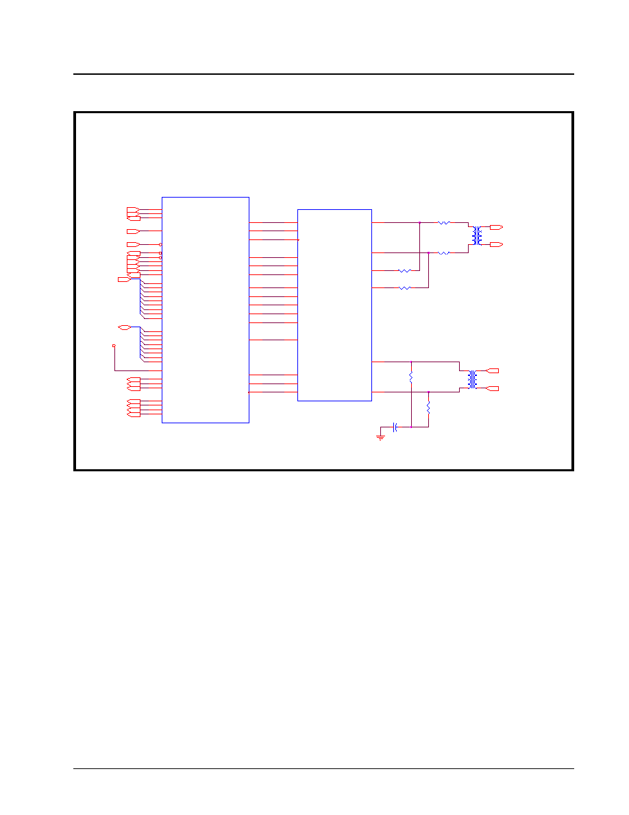
·Á
·Á
·Á
·Á
XRT7250
DS3/E3 FRAMER IC
REV. 1.1.1
377
The Transmit Section of the XRT7250 contains a
block which is known as the Transmit E3 LIU Interface
block. The purpose of the Transmit E3 LIU Interface
block is to take the Outbound E3 data stream, from
the Transmit E3 Framer block, and to do the following:
1. Encode this data into one of the following line
codes
a. Unipolar (e.g., Single-Rail)
b. AMI (Alternate Mark Inversion)
c. HDB3 (High Density Bipolar - 3)
2. And to transmit this data to the LIU IC.
Figure 179 presents a simple illustration of the Trans-
mit E3 LIU Interface block.
F
IGURE
178. A
PPROACH
TO
I
NTERFACING
THE
XRT7250 F
RAMER
IC
DEVICE
TO
THE
XRT7300 DS3/E3/STS-1 LIU
5V
U 1
X R T7250
TxP OS
65
TxN E G
64
TxLineC lk
63
D MO
79
E xtLOS
78
R LOL
77
LLOOP
69
R LOOP
70
TA OS
68
TxLE V
67
E N C OD IS
66
R E QB
71
R xP OS
76
R xN E G
75
R xLineC l k
74
MOTO
27
R E S E TB
28
A 0
15
A 1
16
A 2
17
A 3
18
A 4
19
A 5
20
A 6
21
A 7
22
A 8
23
D 0
32
D 1
33
D 2
34
D 3
35
D 4
36
D 5
37
D 6
38
D 7
39
R dy_D tck
6
W R B _R W
7
R D B _D S
10
C S B
8
A LE _A S
9
IN TB
13
TxS E R
46
TxInC lk
43
TxFrame
61
R xS er
86
R xC lk
88
R xFrame
90
R xLOS
95
R xOOF
94
R xR E D
93
R xA IS
87
N IB B LE IN TF
25
U 2
X R T7300
TP D A TA
37
TN D A TA
38
TC LK
36
R C LK 1
31
R N E G
32
R P OS
33
TTIP
41
TR IN G
40
MTIP
44
MR IN G
43
R R IN G
9
R TIP
8
D MO
4
R LOS
24
R LOL
23
LLB
14
R LB
15
TA OS
2
TxLE V
1
E N C OD IS
21
R E QD IS
12
T1
1:1
1
5
4
8
T2
1:1
1
5
4
8
R 1
36
1
2
R 2
36
1
2
R 6
37.5
1
2
R 3
270
1
2
R 4
270
1
2
R 5
37.5
1
2
C 1
0.01uF
1
2
TxS E R
TxInC lk
N IB B LE IN TF
R E S E TB
R TIP
R R IN G
C S B
R W
D S
A S
TxFrame
R xS er
R xC lk
R xFrame
R xLOS
R xOOF
R xR E D
R xA IS
A [8:0]
TR IN G
TTIP
IN TB
D [7:0]
IN TB

XRT7250
·Á
·Á
·Á
·Á
DS3/E3 FRAMER IC
REV. 1.1.1
378
The Transmit E3 LIU Interface block can transmit data
to the LIU IC or other external circuitry via two differ-
ent output modes: Unipolar or Bipolar. If the user se-
lects Unipolar (or Single Rail) mode, then the con-
tents of the E3 Frame is output, in a binary (NRZ
manner) data stream via the TxPOS pin to the LIU IC.
The TxNEG pin will only be used to denote the frame
boundaries. TxNEG will pulse "High" for one bit peri-
od, at the start of each new E3 frame, and will remain
"Low" for the remainder of the frame. Figure 180 pre-
sents an illustration of the TxPOS and TxNEG signals
during data transmission while the Transmit E3 LIU
Interface block is operating in the Unipolar mode.
This mode is sometimes referred to as Single Rail
mode because the data pulses only exist in one po-
larity: positive.
When the Transmit E3 LIU Interface block is operating
in the Bipolar (or Dual Rail) mode, then the contents
of the E3 Frame is output via both the TxPOS and Tx-
NEG pins. If the Bipolar mode is chosen, then the E3
data can be transmitted to the LIU via one of two dif-
ferent line codes: Alternate Mark Inversion (AMI) or
High Density Bipolar -3 (HDB3). Each one of these
line codes will be discussed below. Bipolar mode is
F
IGURE
179. A S
IMPLE
I
LLUSTRATION
OF
THE
T
RANSMIT
E3 LIU I
NTERFACE
BLOCK
From Transmit E3
Framer Block
TxPOS
TxNEG
TxLineClk
Transmit E3
LIU Interface
Block
F
IGURE
180. T
HE
B
EHAVIOR
OF
T
X
POS
AND
T
X
NEG
SIGNALS
DURING
DATA
TRANSMISSION
WHILE
THE
T
RANSMIT
DS3 LIU I
NTERFACE
IS
OPERATING
IN
THE
U
NIPOLAR
M
ODE
TxPOS
TxNEG
TxLineClk
Data
1 0 1 1 0 0 1 0 0 1 1 1 0 1 0 1 0 0 1 1 1 0 0 1
Frame Boundary
·Á
·Á
·Á
·Á
XRT7250
DS3/E3 FRAMER IC
REV. 1.1.1
379
sometimes referred to as Dual Rail because the data
pulses occur in two polarities: positive and negative.
The role of the TxPOS, TxNEG and TxLineClk output
pins, for this mode are discussed below.
TxPOS - Transmit Positive Polarity Pulse: The
Transmit E3 LIU Interface block will assert this output
to the LIU IC when it desires for the LIU to generate
and transmit a positive polarity pulse to the remote
terminal equipment.
TxNEG - Transmit Negative Polarity Pulse: The
Transmit E3 LIU Interface block will assert this output
to the LIU IC when it desires for the LIU to generate
and transmit a negative polarity pulse to the remote
terminal equipment.
TxLineClk - Transmit Line Clock: The LIU IC uses
this signal from the Transmit E3 LIU Interface block to
sample the state of its TxPOS and TxNEG inputs.
The results of this sampling dictates the type of pulse
(positive polarity, zero, or negative polarity) that it will
generate and transmit to the remote Receive E3
Framer.
6.2.5.1
Selecting the various Line Codes
The user can select either the Unipolar Mode or Bipo-
lar Mode by writing the appropriate value to Bit 3 of
the I/O Control Register (Address = 0x01), as shown
below.
Table 80 relates the value of this bit field to the Trans-
mit E3 LIU Interface Output Mode.
N
OTES
:
1. The default condition is the Bipolar Mode.
2. This selection also effects the operation of the
Receive E3 LIU Interface block
6.2.5.1.1
The Bipolar Mode Line Codes
If the Framer is selected to operate in the Bipolar
Mode, then the DS3 data-stream can be transmitted
via the AMI (Alternate Mark Inversion) or the HDB3
Line Codes. The definition of AMI and HDB3 line
codes follow.
6.2.5.1.1.1
The AMI Line Code
AMI or Alternate Mark Inversion, means that consec-
utive "one's" pulses (or marks) will be of opposite po-
larity with respect to each other. The line code in-
volves the use of three different amplitude levels: +1,
0, and -1. +1 and -1 amplitude signals are used to
represent one's (or mark) pulses and the "0" ampli-
tude pulses (or the absence of a pulse) are used to
represent zeros (or space) pulses. The general rule
for AMI is: if a given mark pulse is of positive polarity,
then the very next mark pulse will be of negative po-
larity and vice versa. This alternating-polarity rela-
tionship exists between two consecutive mark pulses,
independent of the number of 'zeros' that may exist
between these two pulses. Figure 181 presents an il-
lustration of the AMI Line Code as would appear at
the TxPOS and TxNEG pins of the Framer, as well as
the output signal on the line.
I/O CONTROL REGISTER (ADDRESS = 0X01)
B
IT
7
B
IT
6
B
IT
5
B
IT
4
B
IT
3
B
IT
2
B
IT
1
B
IT
0
Disable TxLOC
LOC
Disable
RxLOC
AMI/ZeroSup*
Unipolar/
Bipolar*
TxLine CLK
Invert
RxLine CLK
Invert
Reframe
R/W
RO
R/W
R/W
R/W
R/W
R/W
R/W
1
0
1
0
0
0
0
0
T
ABLE
80: T
HE
R
ELATIONSHIP
BETWEEN
THE
CONTENT
OF
B
IT
3 (U
NIPOLAR
/B
IPOLAR
*)
WITHIN
THE
UNI I/O
C
ONTROL
R
EGISTER
AND
THE
T
RANSMIT
E3 F
RAMER
L
INE
I
NTERFACE
O
UTPUT
M
ODE
B
IT
3
T
RANSMIT
E3 F
RAMER
LIU I
NTERFACE
O
UTPUT
M
ODE
0
Bipolar Mode: AMI or HDB3 Line Codes are Transmitted and Received
1
Unipolar (Single Rail) Mode of transmission and reception of E3 data is selected.
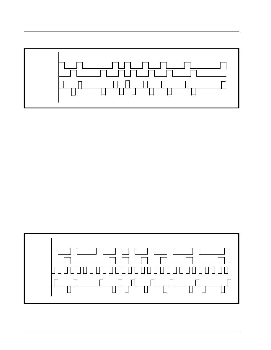
XRT7250
·Á
·Á
·Á
·Á
DS3/E3 FRAMER IC
REV. 1.1.1
380
N
OTE
: One of the main reasons that the AMI Line Code
has been chosen for driving transformer-coupled media is
that this line code introduces no dc component, thereby
minimizing dc distortion in the line.
6.2.5.1.1.2
The HDB3 Line Code
The Transmit E3 Framer and the associated LIU IC
combine the data and timing information (originating
from the TxLineClk signal) into the line signal that is
transmitted to the remote receiver. The remote re-
ceiver has the task of recovering this data and timing
information from the incoming E3 data stream. Many
clock and data recovery schemes rely on the use of
Phase Locked Loop technology. Phase-Locked-Loop
(PLL) technology for clock recovery relies on transi-
tions in the line signal, in order to maintain lock with
the incoming E3 data stream. However, PLL-based
clock recovery scheme, are vulnerable to the occur-
rence of a long stream of consecutive zeros (e.g., the
absence of transitions). This scenario can cause the
PLL to lose lock with the incoming E3 data, thereby
causing the clock and data recovery process of the
receiver to fail. Therefore, some approach is needed
to insure that such a long string of consecutive zeros
can never happen. One such technique is HDB3 en-
coding. HDB3 (or High Density Bipolar - 3) is a form
of AMI line coding that implements the following rule.
In general the HDB3 line code behaves just like AMI
with the exception of the case when a long string of
consecutive zeros occur on the line. Any string of 4
consecutive zeros will be replaced with either a
"000V" or a "B00V" where "B" refers to a Bipolar
pulse (e.g., a pulse with a polarity that is compliant
with the AMI coding rule). And "V" refers to a Bipolar
Violation pulse (e.g., a pulse with a polarity that vio-
lates the alternating polarity scheme of AMI.) The de-
cision between inserting an "000V" or a "B00V" is
made to insure that an odd number of Bipolar (B)
pulses exist between any two Bipolar Violation (V)
pulses. Figure 182 presents a timing diagram that il-
lustrates examples of HDB3 encoding.
The user chooses between AMI or HDB3 line coding
by writing to bit 4 of the I/O Control Register (Address
= 0x01), as shown below.
F
IGURE
181. I
LLUSTRATION
OF
AMI L
INE
C
ODE
Data
TxPOS
TxNEG
Line Signal
1 0 1 1 0 0 0 1 0 1 1 1 1 0 1 1 0 1 1 0 0 1 1 0 0 0 0 1
F
IGURE
182. I
LLUSTRATION
OF
TWO
EXAMPLES
OF
HDB3 E
NCODING
Data
TxPOS
TxNEG
TxLineClk
Line Signal
0
0
0
V
B
0
0
V
1
0
1
1
1
1
1
1
1
1
0
0
0
0
0
0
0
0
1
1
1
0
0
0
0
0
1
1
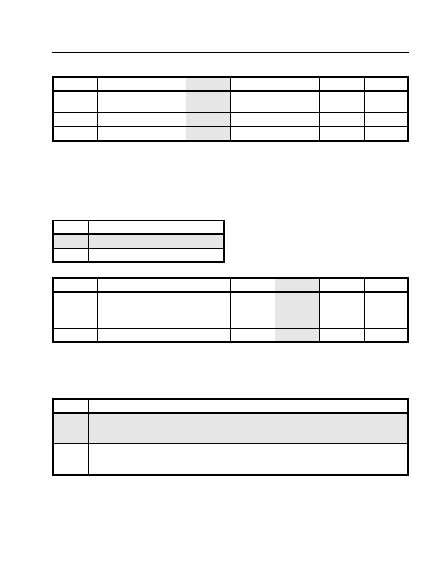
·Á
·Á
·Á
·Á
XRT7250
DS3/E3 FRAMER IC
REV. 1.1.1
381
Table 81 relates the content of this bit-field to the Bi-
polar Line Code which E3 Data will be transmitted
and received at.
N
OTES
:
1. This bit is ignored if the Unipolar mode is selected.
2. This selection also effects the operation of the
Receive E3 LIU Interface block
6.2.5.2
TxLineClk Clock Edge Selection
The Framer also allows the user to specify whether
the E3 output data (via TxPOS and/or TxNEG output
pins) is to be updated on the rising or falling edges of
the TxLineClk signal. This selection is made by writ-
ing to bit 2 of the I/O Control Register, as depicted be-
low.
Table 82 relates the contents of this bit field to the
clock edge of TxClk that E3 Data is output on the Tx-
POS and/or TxNEG output pins.
N
OTE
: The user will typically make the selection based
upon the set-up and hold time requirements of the Transmit
LIU IC.
I/O CONTROL REGISTER (ADDRESS = 0X01)
B
IT
7
B
IT
6
B
IT
5
B
IT
4
B
IT
3
B
IT
2
B
IT
1
B
IT
0
Disable TxLOC
LOC
Disable
RxLOC
AMI/ZeroSup*
Unipolar/
Bipolar*
TxLine CLK
Invert
RxLine CLK
Invert
Reframe
R/W
RO
R/W
R/W
R/W
R/W
R/W
R/W
1
0
1
0
0
0
0
0
T
ABLE
81: T
HE
R
ELATIONSHIP
BETWEEN
B
IT
4 (AMI/
HDB3*)
WITHIN
THE
I/O C
ONTROL
R
EGISTER
AND
THE
B
IPOLAR
L
INE
C
ODE
THAT
IS
OUTPUT
BY
THE
T
RANSMIT
E3 LIU I
NTERFACE
B
LOCK
B
IT
4
B
IPOLAR
L
INE
C
ODE
0
HDB3
1
AMI
II/O CONTROL REGISTER (ADDRESS = 0X01)
B
IT
7
B
IT
6
B
IT
5
B
IT
4
B
IT
3
B
IT
2
B
IT
1
B
IT
0
Disable TxLOC
LOC
Disable
RxLOC
AMI/ZeroSup*
Unipolar/
Bipolar*
TxLine CLK
Invert
RxLine CLK
Invert
Reframe
R/W
RO
R/W
R/W
R/W
R/W
R/W
R/W
1
0
1
0
0
0
0
0
T
ABLE
82: T
HE
R
ELATIONSHIP
BETWEEN
THE
CONTENTS
OF
B
IT
2 (T
X
L
INE
C
LK
I
NV
)
WITHIN
THE
I/O C
ONTROL
R
EGISTER
AND
THE
T
X
L
INE
C
LK
CLOCK
EDGE
THAT
T
X
POS
AND
T
X
NEG
ARE
UPDATED
ON
B
IT
2
R
ESULT
0
Rising Edge:
Outputs on TxPOS and/or TxNEG are updated on the rising edge of TxLineClk.
See Figure 183 for timing relationship between TxLineClk, TxPOS and TxNEG signals, for this selection.
1
Falling Edge:
Outputs on TxPOS and/or TxNEG are updated on the falling edge of TxLineClk.
See Figure 184 for timing relationship between TxLineClk, TxPOS and TxNEG signals, for this selection.
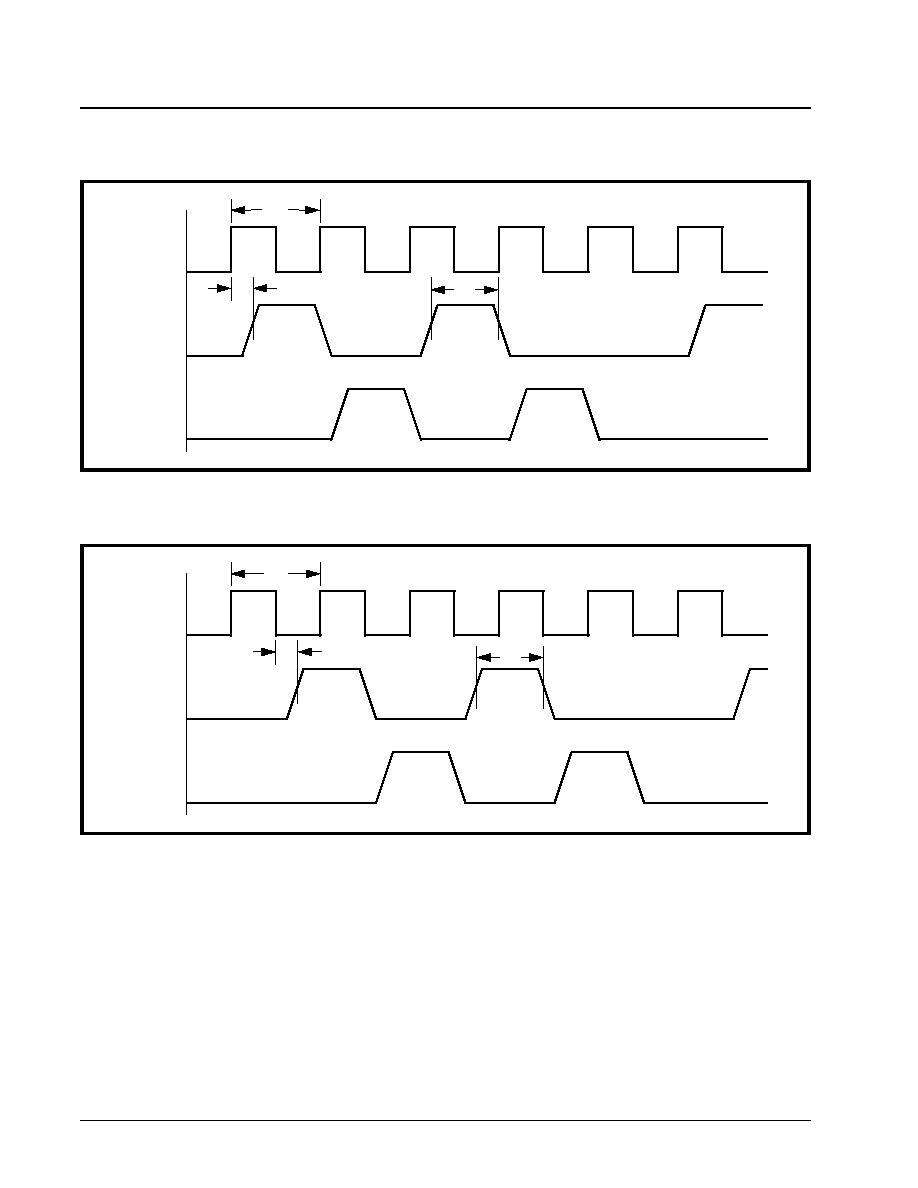
XRT7250
·Á
·Á
·Á
·Á
DS3/E3 FRAMER IC
REV. 1.1.1
382
6.2.6
Transmit Section Interrupt Processing
The Transmit Section of the XRT7250 can generate
an interrupt to the Microprocessor/Microcontroller for
the following reasons.
∑ Completion of Transmission of LAPD Message
6.2.6.1
Enabling Transmit Section Interrupts
As mentioned in Section 36, the Interrupt Structure,
within the XRT7250 contains two hierarchical levels:
∑ Block Level
∑ Source Level
The Block Level
The Enable State of the Block Level for the Transmit
Section Interrupts dictates whether or not interrupts
(enabled) at the source level, are actually enabled.
The user can enable or disable these Transmit Sec-
tion interrupts, at the Block Level by writing the appro-
priate data into Bit 1 (Tx DS3/E3 Interrupt Enable)
within the Block Interrupt Enable register (Address =
0x04), as illustrated below.
F
IGURE
183. W
AVEFORM
/T
IMING
R
ELATIONSHIP
BETWEEN
T
X
L
INE
C
LK
, T
X
POS
AND
T
X
NEG - T
X
POS
AND
T
X
NEG
ARE
CONFIGURED
TO
BE
UPDATED
ON
THE
RISING
EDGE
OF
T
X
L
INE
C
LK
TxLineClk
TxPOS
TxNEG
t32
t30
t33
F
IGURE
184. W
AVEFORM
/T
IMING
R
ELATIONSHIP
BETWEEN
T
X
L
INE
C
LK
, T
X
POS
AND
T
X
NEG - T
X
POS
AND
T
X
NEG
ARE
CONFIGURED
TO
BE
UPDATED
ON
THE
FALLING
EDGE
OF
T
X
L
INE
C
LK
TxLineClk
TxPOS
TxNEG
t31
t32
t33
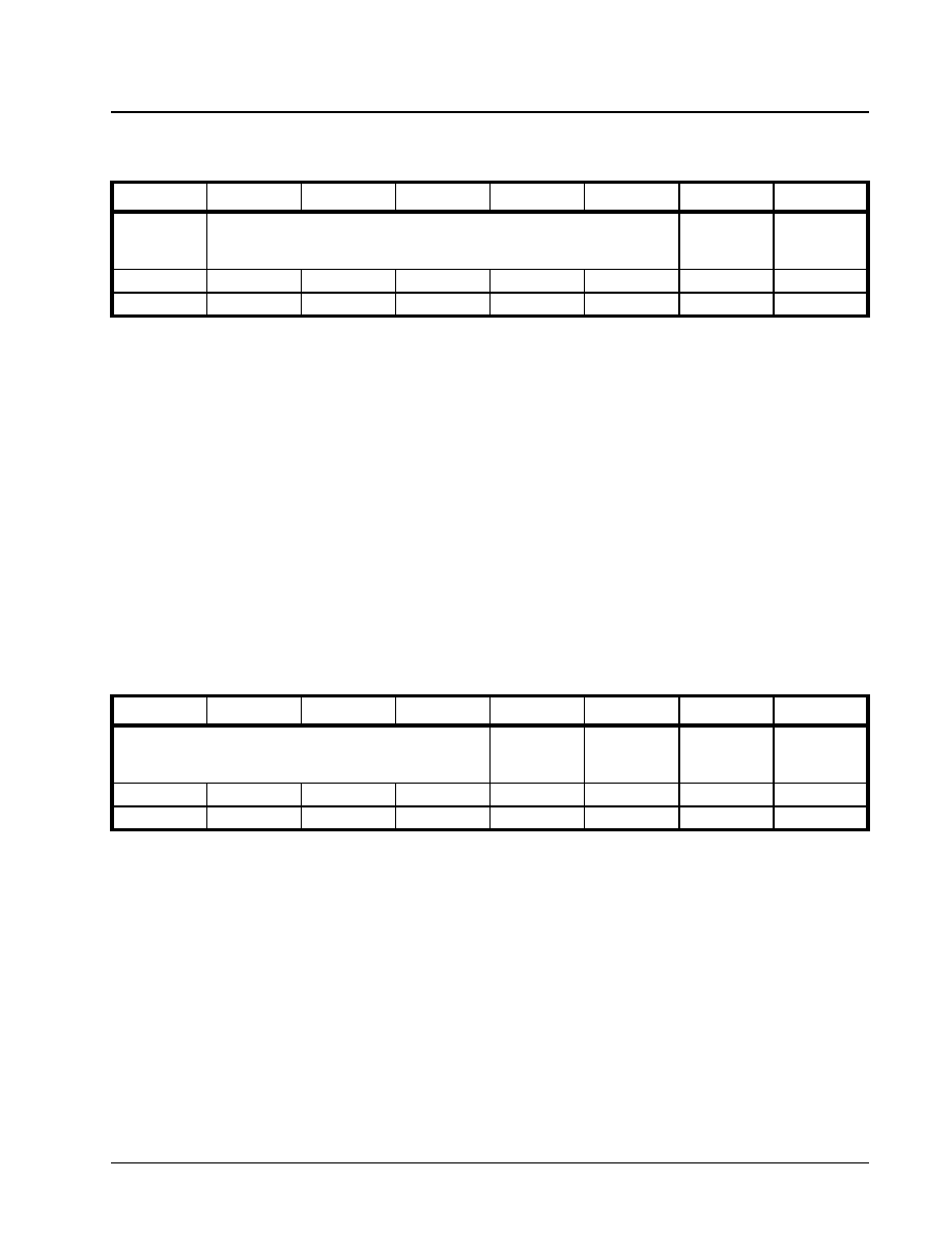
·Á
·Á
·Á
·Á
XRT7250
DS3/E3 FRAMER IC
REV. 1.1.1
383
Setting this bit-field to "1" enables the Transmit Sec-
tion (at the Block Level) for Interrupt Generation.
Conversely, setting this bit-field to "0" disables the
Transmit Section for interrupt generation.
What does it mean for the Transmit Section Inter-
rupts to be enabled or disabled at the Block Lev-
el?
If the Transmit Section is disabled (for interrupt gener-
ation) at the Block Level, then ALL Transmit Section
interrupts are disabled, independent of the interrupt
enable/disable state of the source level interrupts.
If the Transmit Section is enabled (for interrupt gener-
ation) at the block level, then a given interrupt will be
enabled at the source level. Conversely, if the Trans-
mit Section is enabled (for interrupt generation) at the
Block level, then a given interrupt will still be disabled,
if it is disabled at the source level.
As mentioned earlier, the Transmit Section of the
XRT7250 Framer IC contains the Completion of
Transmission of LAPD Message Interrupt.
The Enabling/Disabling and Servicing of this interrupt
is presented below.
6.2.6.1.1
The Completion of Transmission of
the LAPD Message Interrupt
If the Transmit Section interrupts have been enabled
at the Block level, then the user can enable or disable
the Completion of Transmission of a LAPD Message
Interrupt by writing the appropriate value into Bit 1
(TxLAPD Interrupt Enable) within the Tx E3 LAPD
Status & Interrupt Register (Address = 0x34), as illus-
trated below.
Setting this bit-field to "1" enables the Completion of
Transmission of a LAPD Message Interrupt. Con-
versely, setting this bit-field to "0" disables the Com-
pletion of Transmission of a LAPD Message interrupt.
6.2.6.1.2
Servicing the Completion of Trans-
mission of a LAPD Message Interrupt
As mentioned previously, once the user commands
the LAPD Transmitter to begin its transmission of a
LAPD Message, it will do the following.
1. It will parse through the contents of the Transmit
LAPD Message Buffer (located at address loca-
tions 0x86 through 0xDD) and search for a string
of five (5) consecutive "1's". If the LAPD Trans-
mitter finds a string of five consecutive "1's"
(within the content of the LAPD Message Buffer,
then it will insert a "0" immediately after this
string.
2. It will compute the FCS (Frame Check Sequence)
value and append this value to the back-end of
the user-message.
3. It will read out of the content of the user (zero-
stuffed) message and will encapsulate this data
into a LAPD Message frame.
4. Finally, it will begin transmitting the contents of
this LAPD Message frame via the "N" bits, within
each Outbound E3 frame.
5. Once the LAPD Transmitter has completed its
transmission of this LAPD Message frame (to the
Remote Terminal Equipment), the XRT7250
Framer IC will generate the Completion of Trans-
BLOCK INTERRUPT ENABLE REGISTER (ADDRESS = 0X04)
B
IT
7
B
IT
6
B
IT
5
B
IT
4
B
IT
3
B
IT
2
B
IT
1
B
IT
0
RxDS3/E3
Interrupt
Enable
Not Used
TxDS3/E3
Interrupt
Enable
One-Second
Interrupt
Enable
R/W
RO
RO
RO
RO
RO
R/W
R/W
0
0
0
0
0
0
0
0
TXE3 LAPD STATUS AND INTERRUPT REGISTER (ADDRESS = 0X34)
B
IT
7
B
IT
6
B
IT
5
B
IT
4
B
IT
3
B
IT
2
B
IT
1
B
IT
0
Not Used
TXDL Start
TXDL Busy
TxLAPD
Interrupt
Enable
TxLAPD
Interrupt
Status
RO
RO
RO
RO
R/W
RO
R/W
RUR
0
0
0
0
0
0
X
0
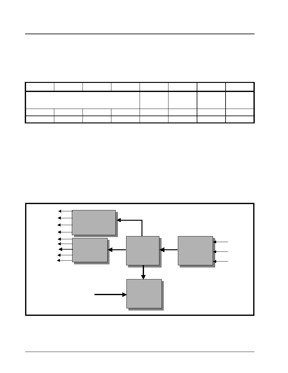
XRT7250
·Á
·Á
·Á
·Á
DS3/E3 FRAMER IC
REV. 1.1.1
384
mission of a LAPD Message Interrupt to the
Microcontroller/Microprocessor. Once the
XRT7250 Framer IC generates this interrupt, it
will do the following.
∑ Assert the Interrupt Output pin (INT) by toggling it
"Low".
∑ Set Bit 0 (TxLAPD Interrupt Status) within the TxE3
LAPD Status and Interrupt Register, to "1" as illus-
trated below.
The purpose of this interrupt is to alert the Microcon-
troller/MIcroprocessor that the LAPD Transmitter has
completed its transmission of a given LAPD (or PM-
DL) Message, and is now ready to transmit the next
PMDL Message, to the Remote Terminal Equipment.
6.3
T
HE
R
ECEIVE
S
ECTION
OF
THE
XRT7250 (E3
M
ODE
O
PERATION
)
When the XRT7250 has been configured to operate
in the E3 Mode, the Receive Section of the XRT7250
consists of the following functional blocks.
∑ Receive LIU Interface block
∑ Receive HDLC Controller block
∑ Receive E3 Framer block
∑ Receive Overhead Data Output Interface block
∑ Receive Payload Data Output Interface block
Figure 185 presents a simple illustration of the Re-
ceive Section of the XRT7250 Framer IC.
Each of these functional blocks will be discussed in
detail in this document.
6.3.1
The Receive E3 LIU Interface Block
The purpose of the Receive E3 LIU Interface block is
two-fold:
1. To receive encoded digital data from the E3 LIU
IC.
TXE3 LAPD STATUS AND INTERRUPT REGISTER (ADDRESS = 0X34)
B
IT
7
B
IT
6
B
IT
5
B
IT
4
B
IT
3
B
IT
2
B
IT
1
B
IT
0
Not Used
TXDL Start
TXDL Busy
TxLAPD
Interrupt
Enable
TxLAPD
Interrupt
Status
RO
RO
RO
RO
R/W
RO
R/W
RUR
0
0
0
0
0
0
0
1
F
IGURE
185. A S
IMPLE
I
LLUSTRATION
OF
THE
R
ECEIVE
S
ECTION
OF
THE
XRT7250,
WHEN
IT
HAS
BEEN
CONFIG
-
URED
TO
OPERATE
IN
THE
E3 M
ODE
Receive
Payload Data
Input
Interface Block
Receive DS3/E3
Framer Block
Receive LIU
Interface
Block
RxSer
RxNib[3:0]
RxClk
RxPOS
RxNEG
RxLineClk
Receive Overhead
Input
Interface Block
RxOHClk
RxOHInd
RxOH
RxOHEnable
RxOHFrame
RxFrame
Rx E3 HDLC
Controller/Buffer
Rx E3 HDLC
Controller/Buffer
From Microprocessor
Interface Block
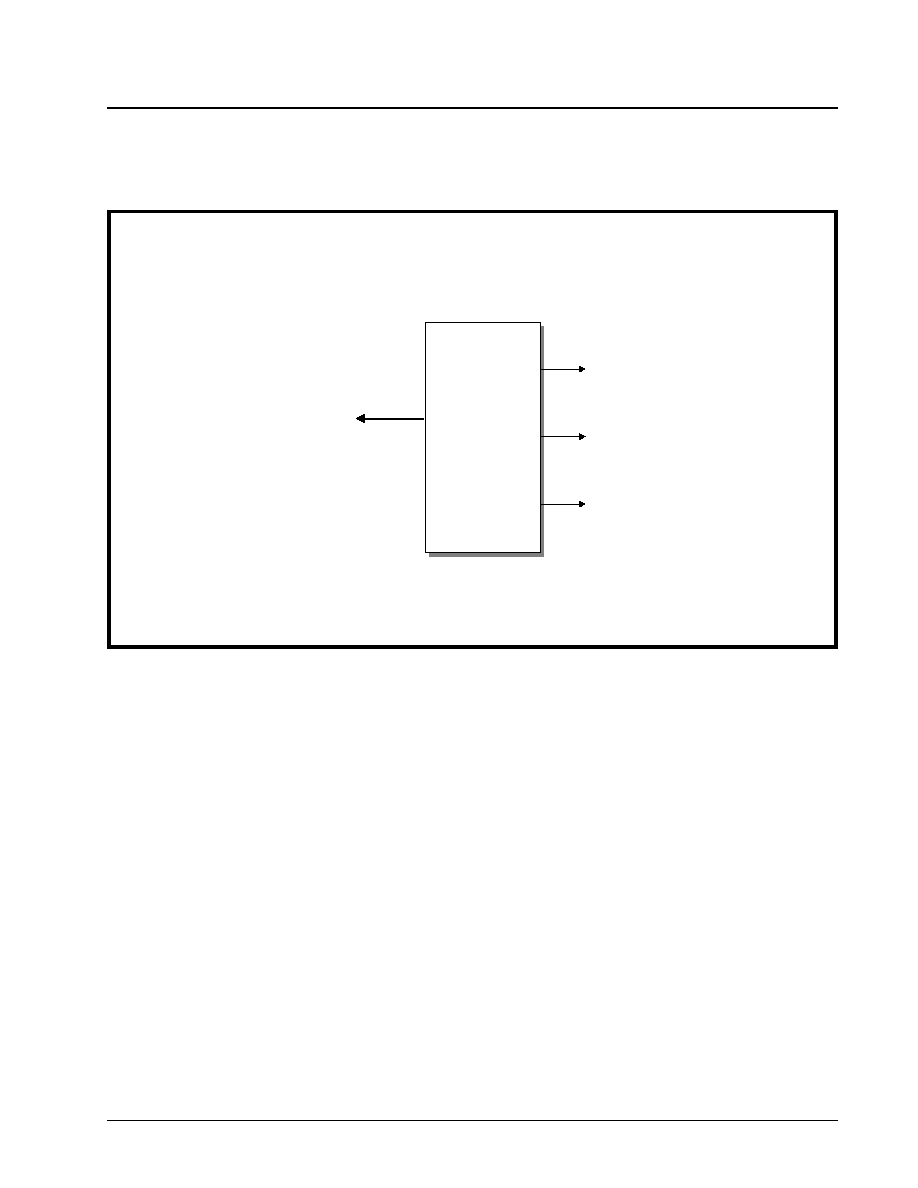
·Á
·Á
·Á
·Á
XRT7250
DS3/E3 FRAMER IC
REV. 1.1.1
385
2. To decode this data, convert it into a binary data
stream and to route this data to the Receive E3
Framer block.
Figure 186 presents a simple illustration of the Re-
ceive E3 LIU Interface block.
The Receive Section of the XRT7250 will via the Re-
ceive E3 LIU Interface Block receive timing and data
information from the incoming E3 data stream. The
E3 Timing information will be received via the RxLi-
neClk input pin and the E3 data information will be re-
ceived via the RxPOS and RxNEG input pins. The
Receive E3 LIU Interface block is capable of receiving
E3 data pulses in unipolar or bipolar format. If the
Receive E3 framer is operating in the bipolar format,
then it can be configured to decode either AMI or
HDB3 line code data. Each of these input formats
and line codes will be discussed in detail, below.
6.3.1.1
Unipolar Decoding
If the Receive E3 LIU Interface block is operating in
the Unipolar (single-rail) mode, then it will receive the
Single Rail NRZ DS3 data pulses via the RxPOS in-
put pin. The Receive E3 LIU Interface block will also
receive its timing signal via the RxLineClk signal.
N
OTE
: The RxLineClk signal will function as the timing
source for the entire Receive Section of the XRT7250.
No data pulses will be applied to the RxNEG input
pin. The Receive E3 LIU Interface block receives a
logic "1" when a logic "1" level signal is present at the
RxPOS pin, during the sampling edge of the RxLi-
neClk signal. Likewise, a logic "0" is received when a
logic "0" level signal is applied to the RxPOS pin.
Figure 187 presents an illustration of the behavior of
the RxPOS, RxNEG and RxLineClk input pins when
the Receive E3 LIU Interface block is operating in the
Unipolar mode.
F
IGURE
186. A S
IMPLE
I
LLUSTRATION
OF
THE
R
ECEIVE
E3 LIU I
NTERFACE
B
LOCK
RxPOS
RxNEG
RxLineClk
To Receive DS3
Framer Block
Receive DS3
LIU Interface
Block
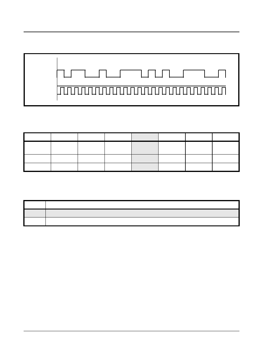
XRT7250
·Á
·Á
·Á
·Á
DS3/E3 FRAMER IC
REV. 1.1.1
386
The user can configure the Receive E3 LIU Interface
block to operate in either the Unipolar or the Bipolar
Mode by writing the appropriate data to the I/O Con-
trol Register, as depicted below.
Table 83 relates the value of this bit-field to the Re-
ceive E3 LIU Interface Input Mode.
N
OTES
:
1. The default condition is the Bipolar Mode.
2. This selection also effects the Transmit E3 Framer
Line Interface Output Mode
6.3.1.2
Bipolar Decoding
If the Receive E3 LIU Interface block is operating in
the Bipolar Mode, then it will receive the E3 data puls-
es via both the RxPOS, RxNEG, and the RxLineClk
input pins. Figure 188 presents a circuit diagram il-
lustrating how the Receive E3 LIU Interface block in-
terfaces to the Line Interface Unit while the Framer is
operating in Bipolar mode. The Receive E3 LIU Inter-
face block can be configured to decode either the AMI
or HDB3 line codes.
F
IGURE
187. B
EHAVIOR
OF
THE
R
X
POS, R
X
NEG
AND
R
X
L
INE
C
LK
SIGNALS
DURING
DATA
RECEPTION
OF
U
NIPO
-
LAR
D
ATA
RxPOS
RxNEG
RxLineClk
Data
1 0 1 1 0 0 1 0 0 1 1 1 0 1 0 1 0 0 1 1 1 0 0 1
II/O CONTROL REGISTER (ADDRESS = 0X01)
B
IT
7
B
IT
6
B
IT
5
B
IT
4
B
IT
3
B
IT
2
B
IT
1
B
IT
0
Disable TxLOC
LOC
Disable
RxLOC
AMI/ZeroSup*
Unipolar/
Bipolar*
TxLine CLK
Invert
RxLine CLK
Invert
Reframe
R/W
RO
R/W
R/W
R/W
R/W
R/W
R/W
1
0
1
0
0
0
0
0
T
ABLE
83: T
HE
R
ELATIONSHIP
BETWEEN
THE
CONTENTS
OF
B
IT
2 (T
X
L
INE
C
LK
I
NV
)
WITHIN
THE
I/O C
ONTROL
R
EGISTER
AND
THE
T
X
L
INE
C
LK
CLOCK
EDGE
THAT
T
X
POS
AND
T
X
NEG
ARE
UPDATED
ON
B
IT
3
R
ECEIVE
E3 LIU I
NTERFACE
I
NPUT
M
ODE
0
.Bipolar Mode (Dual Rail): AMI or HDB3 Line Codes are Transmitted and Received.
1
Unipolar Mode (Single Rail) Mode of transmission and reception of E3 data is selected.
·Á
·Á
·Á
·Á
XRT7250
DS3/E3 FRAMER IC
REV. 1.1.1
387
6.3.1.2.1
AMI Decoding
AMI or Alternate Mark Inversion, means that consec-
utive "one's" pulses (or marks) will be of opposite po-
larity with respect to each other. This line code in-
volves the use of three different amplitude levels: +1,
0, and -1. The +1 and -1 amplitude signals are used
to represent one's (or mark) pulses and the "0" ampli-
tude pulses (or the absence of a pulse) are used to
represent zeros (or space) pulses. The general rule
for AMI is: if a given mark pulse is of positive polarity,
then the very next mark pulse will be of negative po-
larity and vice versa. This alternating-polarity rela-
tionship exists between two consecutive mark pulses,
independent of the number of zeros that exist be-
tween these two pulses. Figure 189 presents an illus-
tration of the AMI Line Code as would appear at the
RxPOS and RxNEG pins of the Framer, as well as the
output signal on the line.
F
IGURE
188. I
LLUSTRATION
ON
HOW
THE
R
ECEIVE
E3 F
RAMER
(
WITHIN
THE
XRT7250 F
RAMER
IC)
BEING
INTER
-
FACE
TO
THE
XRT7300 L
INE
I
NTERFACE
U
NIT
,
WHILE
THE
F
RAMER
IS
OPERATING
IN
B
IPOLAR
M
ODE
5 V
U 1
XRT7250
TxPOS
65
TxNEG
64
TxLineClk
63
D M O
79
ExtLOS
78
R L O L
77
L L O O P
69
R L O O P
70
T A O S
68
TxLEV
67
E N C O D I S
66
R E Q B
71
RxPOS
76
R x N E G
75
RxLineClk
74
M O T O
27
R E S E T B
28
A 0
15
A 1
16
A 2
17
A 3
18
A 4
19
A 5
20
A 6
21
A 7
22
A 8
23
D 0
32
D 1
33
D 2
34
D 3
35
D 4
36
D 5
37
D 6
38
D 7
39
Rdy_Dtck
6
W R B _ R W
7
R D B _ D S
10
C S B
8
A L E _ A S
9
INTB
13
TxSER
46
TxInClk
43
TxFrame
61
RxSer
86
RxClk
88
RxFrame
90
RxLOS
95
R x O O F
94
RxRED
93
RxAIS
87
NIBBLEINTF
25
U 2
XRT7300
TPDATA
37
T N D A T A
38
TCLK
36
R C L K 1
31
R N E G
32
R P O S
33
TTIP
41
TRING
40
MTIP
44
MRING
43
R R I N G
9
RTIP
8
D M O
4
R L O S
24
R L O L
23
LLB
14
R L B
15
T A O S
2
TxLEV
1
E N C O D I S
21
R E Q D I S
12
T1
1:1
1
5
4
8
T2
1:1
1
5
4
8
R 1
36
1
2
R 2
36
1
2
R 6
37.5
1
2
R 3
270
1
2
R 4
270
1
2
R 5
37.5
1
2
C 1
0.01uF
1
2
TxSER
TxInClk
NIBBLEINTF
R E S E T B
RTIP
R R I N G
C S B
R W
D S
A S
TxFrame
RxSer
RxClk
RxFrame
RxLOS
R x O O F
RxRED
RxAIS
A[8:0]
TRING
TTIP
INTB
D[7:0]
INTB
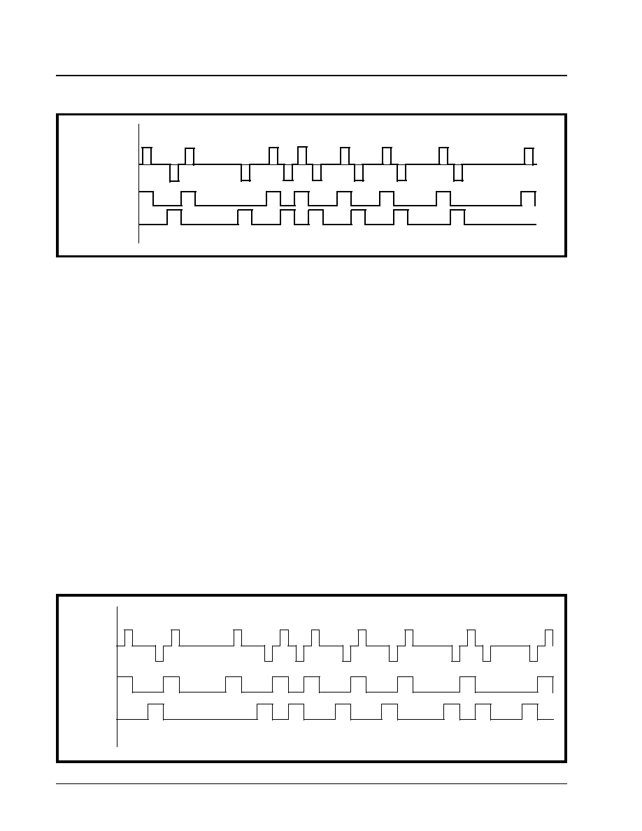
XRT7250
·Á
·Á
·Á
·Á
DS3/E3 FRAMER IC
REV. 1.1.1
388
N
OTE
: One of the reasons that the AMI Line Code has
been chosen for driving copper medium, isolated via trans-
formers, is that this line code has no dc component, thereby
eliminating dc distortion in the line.
6.3.1.2.2
HDB3 Decoding
The Transmit E3 LIU Interface block and the associat-
ed LIU embed and combine the data and clocking in-
formation into the line signal that is transmitted to the
remote terminal equipment. The remote terminal
equipment has the task of recovering this data and
timing information from the incoming E3 data stream.
Most clock and data recovery schemes rely on the
use of Phase-Locked-Loop technology. One of the
problems of using Phase-Locked-Loop (PLL) technol-
ogy for clock recovery is that it relies on transitions in
the line signal, in order to maintain lock with the in-
coming E3 data-stream. Therefore, these clock re-
covery scheme, are vulnerable to the occurrence of a
long stream of consecutive zeros (e.g., no transitions
in the line). This scenario can cause the PLL to lose
lock with the incoming E3 data, thereby causing the
clock and data recovery process of the receiver to fail.
Therefore, some approach is needed to insure that
such a long string of consecutive zeros can never
happen. One such technique is HDB3 (or High Den-
sity Bipolar -3) encoding.
In general the HDB3 line code behaves just like AMI
with the exception of the case when a long string of
consecutive zeros occurs on the line. Any 4 consecu-
tive zeros will be replaced with either a "000V" or a
"B00V" where "B" refers to a Bipolar pulse (e.g., a
pulse with a polarity that is compliant with the AMI
coding rule). And "V" refers to a Bipolar Violation
pulse (e.g., a pulse with a polarity that violates the al-
ternating polarity scheme of AMI.) The decision be-
tween inserting an "000V" or a "B00V" is made to in-
sure that an odd number of Bipolar (B) pulses exist
between any two Bipolar Violation (V) pulses. The
Receive E3 LIU Interface block, when operating with
the HDB3 Line Code is responsible for decoding the
HD-encoded data back into a unipolar (binary-for-
mat). For instance, if the Receive E3 LIU Interface
block detects a "000V" or a "B00V" pattern in the in-
coming pattern, the Receive E3 LIU Interface block
will replace it with four (4) consecutive zeros.
Figure 190 presents a timing diagram that illustrates
examples of HDB3 decoding.
F
IGURE
189. I
LLUSTRATION
OF
AMI L
INE
C
ODE
Data 1 0 1 1 0 0 0 1 0 1 1 1 1 0 1 1 0 1 1 0 0 1 1 0 0 0 0 1
RxPOS
RxNEG
Line Signal
F
IGURE
190. I
LLUSTRATION
OF
TWO
EXAMPLES
OF
HDB3 D
ECODING
Line Signal
0
0
0
V
B
0
0
V
RxNEG
RxPOS
Data
1
0
1
1
1
1
1
1
1
1
0
0
0
0
0
0
0
0
1
1
1
0
0
0
0
0
1
1
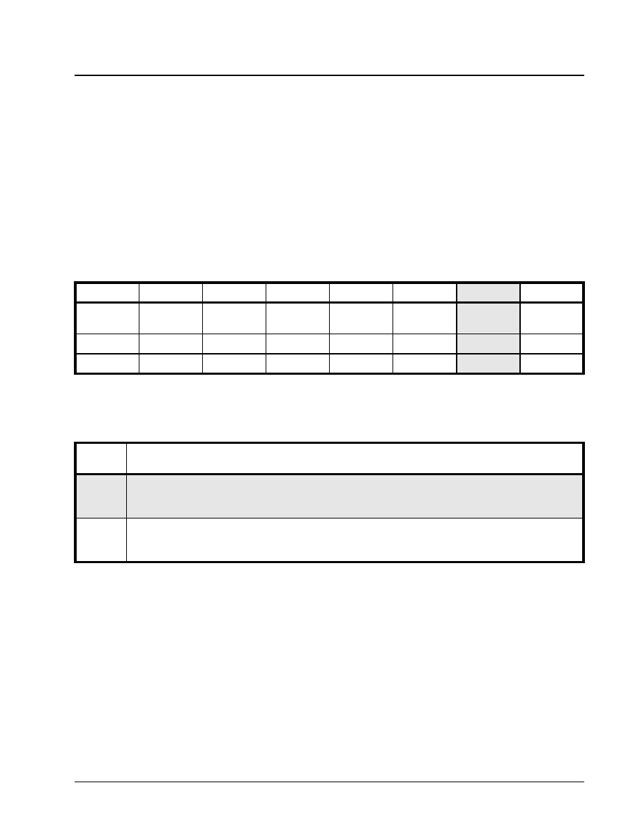
·Á
·Á
·Á
·Á
XRT7250
DS3/E3 FRAMER IC
REV. 1.1.1
389
6.3.1.2.3
Line Code Violations
The Receive E3 LIU Interface block will also check
the incoming E3 data stream for line code violations.
For example, when the Receive E3 LIU Interface
block detects a valid bipolar violation (e.g., in HDB3
line code), it will substitute four zeros into the binary
data stream. However, if the bipolar violation is in-
valid, then an LCV (Line Code Violation) is flagged
and the PMON LCV Event Count Register (Address =
0x50 and 0x51) will also be incremented. Additional-
ly, the LCV-One-Second Accumulation Registers
(Address = 0x6E and 0x6F) will be incremented. For
example: If the incoming E3 data is HDB3 encoded,
the Receive E3 LIU Interface block will also increment
the LCV One-Second Accumulation Register if three
(or more) consecutive zeros are received.
6.3.1.2.4
RxLineClk Clock Edge Selection
The incoming unipolar or bipolar data, applied to the
RxPOS and the RxNEG input pins are clocked into
the Receive E3 LIU Interface block via the RxLineClk
signal. The Framer IC allows the user to specify
which edge (e.g, rising or falling) of the RxLineClk
signal will sample and latch the signal at the RxPOS
and RxNEG input signals into the Framer IC. The us-
er can make this selection by writing the appropriate
data to bit 1 of the I/O Control Register, as depicted
below.
Table 84 depicts the relationship between the value of
this bit-field to the sampling clock edge of RxLineClk.
Figure 191 and Figure 192 present the Waveform and
Timing Relationships between RxLineClk, RxPOS
and RxNEG for each of these configurations.
II/O CONTROL REGISTER (ADDRESS = 0X01)
B
IT
7
B
IT
6
B
IT
5
B
IT
4
B
IT
3
B
IT
2
B
IT
1
B
IT
0
Disable
TxLOC
LOC
Disable
RxLOC
AMI/ZeroSup*
Unipolar/
Bipolar*
TxLine CLK
Invert
RxLine CLK
Invert
Reframe
R/W
RO
R/W
R/W
R/W
R/W
R/W
R/W
1
0
1
0
0
0
0
0
T
ABLE
84: T
HE
R
ELATIONSHIP
BETWEEN
THE
CONTENTS
OF
B
IT
1 (R
X
L
INE
C
LK
I
NV
)
OF
THE
I/O C
ONTROL
R
EGISTER
,
AND
THE
SAMPLING
EDGE
OF
THE
R
X
L
INE
C
LK
SIGNAL
R
X
CLKI
NV
(B
IT
1)
R
ESULT
0
.Rising Edge:
RxPOS and RxNEG are sampled at the rising edge of RxLineClk. See Figure 191 for timing relationship
between RxLineClk, RxPOS, and RxNEG.
1
Falling Edge:
RxPOS and RxNEG are sampled at the falling edge of RxLineClk. See Figure 192 for timing relationship
between RxLineClk, RxPOS, and RxNEG.
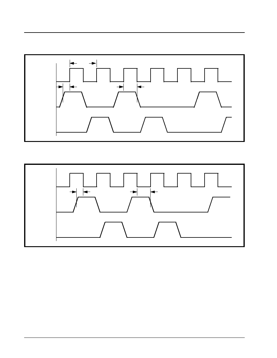
XRT7250
·Á
·Á
·Á
·Á
DS3/E3 FRAMER IC
REV. 1.1.1
390
6.3.2
The Receive E3 Framer Block
The Receive E3 Framer block accepts decoded E3
data from the Receive E3 LIU Interface block, and
routes data to the following destinations.
∑ The Receive Payload Data Output Interface Block
∑ The Receive Overhead Data Output Interface
Block.
∑ The Receive E3 HDLC Controller Block
Figure 193 presents a simple illustration of the Re-
ceive E3 Framer block, along with the associated
paths to the other functional blocks within the Framer
chip.
F
IGURE
191. W
AVEFORM
/T
IMING
R
ELATIONSHIP
BETWEEN
R
X
L
INE
C
LK
, R
X
POS
AND
R
X
NEG - W
HEN
R
X
POS
AND
R
X
NEG
ARE
TO
BE
SAMPLED
ON
THE
RISING
EDGE
OF
R
X
L
INE
C
LK
RxLineClk
RxPOS
RxNEG
t38
t39
t42
F
IGURE
192. W
AVEFORM
/T
IMING
R
ELATIONSHIP
BETWEEN
R
X
L
INE
C
LK
, R
X
POS
AND
R
X
NEG - W
HEN
R
X
POS
AND
R
X
NEG
ARE
TO
BE
SAMPLED
ON
THE
FALLING
EDGE
OF
R
X
L
INE
C
LK
RxLineClk
RxPOS
RxNEG
t40
t41
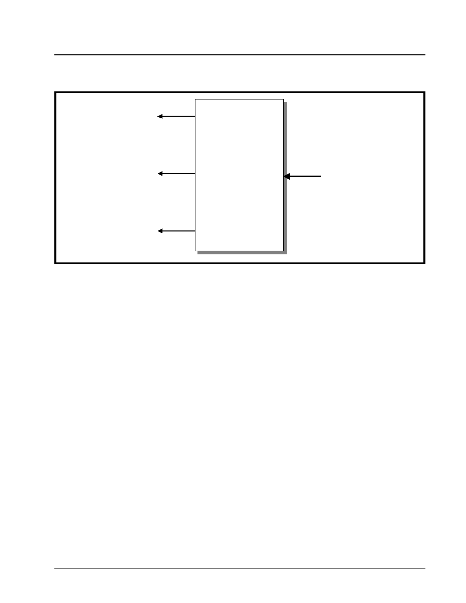
·Á
·Á
·Á
·Á
XRT7250
DS3/E3 FRAMER IC
REV. 1.1.1
391
Once the HDB3 (or AMI) encoded data has been de-
coded into a binary data-stream, the Receive E3
Framer block will use portions of this data-stream in
order to synchronize itself to the remote terminal
equipment. At any given time, the Receive E3 Fram-
er block will be operating in one of two modes.
∑ The Frame Acquisition Mode: In this mode, the
Receive E3 Framer block is trying to acquire syn-
chronization with the incoming E3 frame, or
∑ The Frame Maintenance Mode: In this mode, the
Receive E3 Framer block is trying to maintain frame
synchronization with the incoming E3 Frames.
Figure 194 presents a State Machine diagram that
depicts the Receive E3 Framer block's E3/ITU-T
G.832 Frame Acquisition/Maintenance Algorithm.
6.3.2.1
The Framing Acquisition Mode
The Receive E3 Framer block is considered to be op-
erating in the Frame Acquisition Mode, if it is operat-
ing in any one of the following states within the E3
Frame Acquisition/Maintenance Algorithm per
Figure 194.
∑ FA1, FA2 Octet Search State
∑ FA1, FA2 Octet Verification State
∑ OOF Condition State
∑ LOF Condition State
Each of these Framing Acquisition states, within the
Receive E3 Framer Framing Acquisition/Maintenance
State Machine are discussed below.
The FA1, FA2 Octet Search State
When the Receive E3 Framer block is first powered
up, it will be operating in the FA1, FA2 Octet Search
state. While the Receive E3 Framer is operating in
this state, it will be performing a bit-by-bit search for
the FA1 and FA2 Framing Alignment octets. FA1 is
assigned the value "0xF6", and FA2 is assigned the
value of "0x28". Figure 195, which presents an illus-
tration of the E3, ITU-T G.832 Framing Format, indi-
cates that these two octets will occur at the beginning
of each E3 frame, and that the FA2 octet will appear
immediately after the FA1 octet.
F
IGURE
193. A S
IMPLE
I
LLUSTRATION
OF
THE
R
ECEIVE
E3 F
RAMER
B
LOCK
AND
THE
A
SSOCIATED
P
ATHS
TO
THE
O
THER
F
UNCTIONAL
B
LOCKS
Receive E3 Framer
Block
Receive E3 Framer
Block
To Receive E3 HDLC
Buffer
Receive Overhead Data
Output Interface
Receive Payload Data
Output Interface
From Receive E3
LIU Interface Block
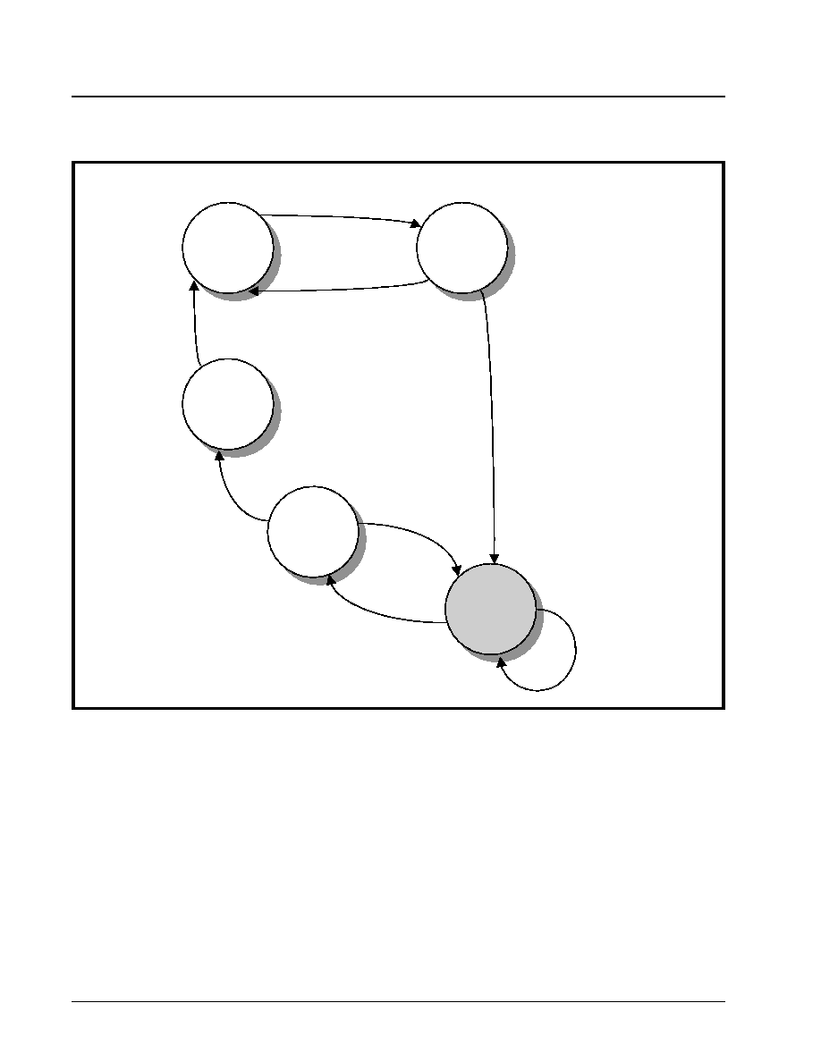
XRT7250
·Á
·Á
·Á
·Á
DS3/E3 FRAMER IC
REV. 1.1.1
392
F
IGURE
194. T
HE
S
TATE
M
ACHINE
D
IAGRAM
FOR
THE
R
ECEIVE
E3 F
RAMER
E3 F
RAME
A
CQUISITION
/M
AINTENANCE
A
LGORITHM
FA1, FA2
Octet
Search
FA1, FA2
Octet
Verification
In Frame
OOF
Condition
LOF
Condition
FA1 and FA2 octets are
detected once
FA1 and FA2 octets
are verified once
FA1 and FA2 octets are
not detected
4 consecutive
In-valid Frames
3 consecutive
Valid Frames
1 or 3 ms of operating
in the OOF condition
(user-selectable)
Frame Maintenance
Mode
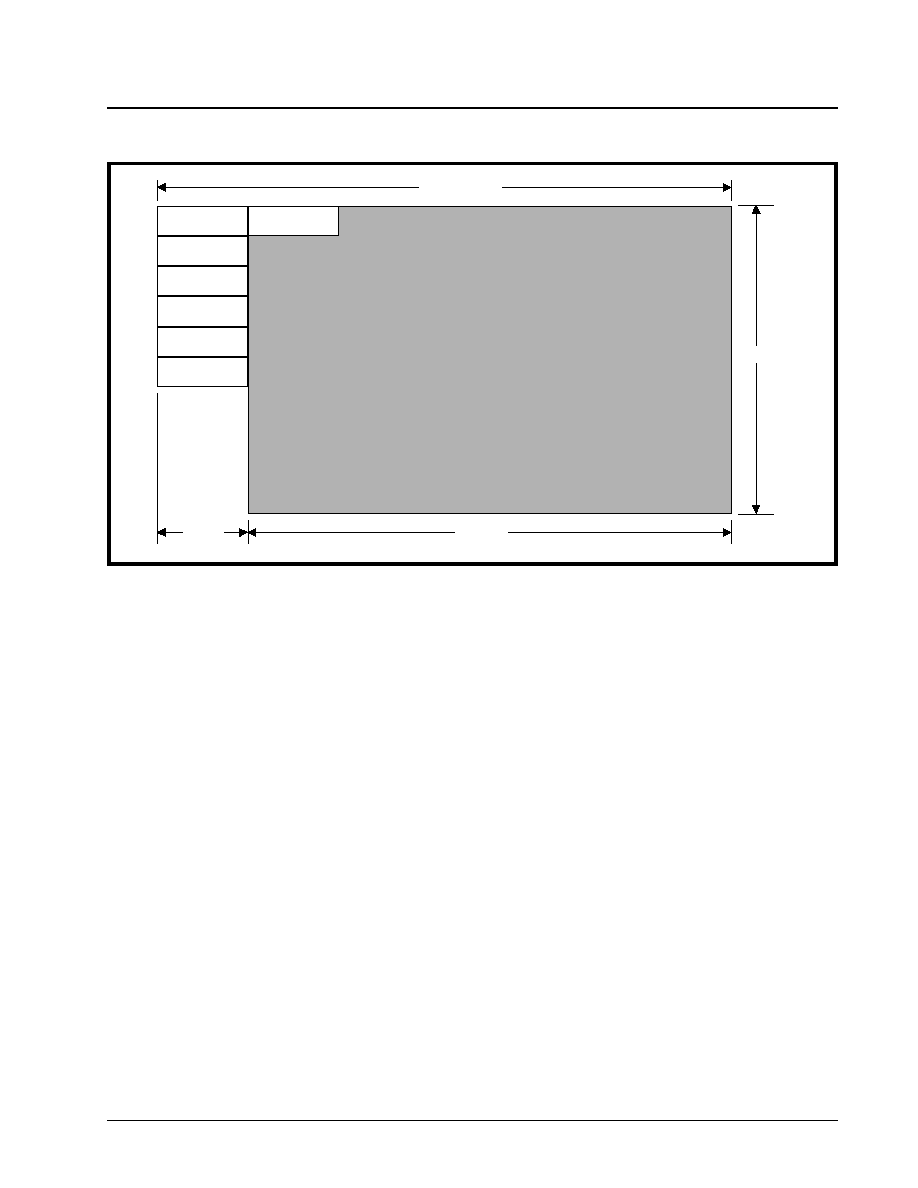
·Á
·Á
·Á
·Á
XRT7250
DS3/E3 FRAMER IC
REV. 1.1.1
393
When the Receive E3 Framer block detects the "FA1"
octet, and determines that this octet is immediately
followed by the "FA2" octet, then it will transition to the
FA1, FA2 Octet Verification state, per Figure 195.
The FA1, FA2 Octet Verification State
Once the Receive E3 Framer block has detected an
"0xF628" pattern (e.g., the concatenation of the FA1
and FA2 octets), it must verify that this pattern is in-
deed the "FA1" and "FA2" octets and not some other
set of bytes, within the E3 frame, mimicking the
Frame Alignment bytes. Hence, the purpose of the
FA1, FA2 Octet Verification state.
When the Receive E3 Framer block enters this state,
it will then quit performing its bit-by-bit search for the
Frame Alignment bytes. Instead, the Receive E3
Framer block will read in the two octets that occur 537
bytes (e.g., one E3 frame period later) after the candi-
date Frame Alignment patterns were first detected. If
these two bytes match the assigned values for the
"FA1" and "FA2" octets, then the Receive E3 Framer
block will conclude that it has found the Frame Align-
ment bytes and will then transition to the In-Frame
state. However, if these two bytes do not match the
assigned values for the "FA1" and "FA2" octets then
the Receive E3 Framer block will concluded that it
has been fooled by data mimicking the Frame Align-
ment bytes, and will transition back to the FA1, FA2
Octet Search state.
In Frame State
Once the Receive E3 Framer block enters the In-
Frame state, then it will cease performing Frame Ac-
quisition functions, and will proceed to perform Fram-
ing Maintenance functions. Therefore, the operation
of the Receive E3 Framer block, while operating in
the In-Frame state, can be found in Section 5.3.2.2
(The Framing Maintenance Mode).
OOF (Out of Frame) Condition State
If the Receive E3 Framer while operating in the In-
Frame state detects four (4) consecutive frames,
which do not have the valid Frame Alignment (FA1
and FA2 octet) patterns, then it will transition into the
OOF Condition State. The Receive E3 Framer
block's operation, while in the OOF condition state is
a unique mix of Framing Maintenance and Framing
Acquisition operation. The Receive E3 Framer block
will exhibit some Framing Acquisition characteristics
by attempting to locate (once again) the Frame Align-
ment octets. However, the Receive E3 Framer block
will also exhibit some Frame Maintenance behavior
by still using the most recent frame synchronization
for its overhead byte and payload byte processing.
The Receive E3 Framer block will inform the Micro-
processor/Microcontroller of its transition from the In-
Frame state to the OOF Condition state, by generat-
ing a Change in OOF Condition Interrupt. When this
occurs, Bit 3 (OOF Interrupt Status), within the Rx E3
F
IGURE
195. I
LLUSTRATION
OF
THE
E3, ITU-T G.832 F
RAMING
F
ORMAT
FA1
FA2
EM
TR
MA
1 Byte
59 Bytes
60 Columns
9 Rows
530 Octet Payload
GC
NR

XRT7250
·Á
·Á
·Á
·Á
DS3/E3 FRAMER IC
REV. 1.1.1
394
Interrupt Status Register - 1, will be set to "1", as de-
picted below.
The Receive E3 Framer block will also inform the ex-
ternal circuitry of its transition into the OOF Condition
state, by toggling the RxOOF output pin "High".
If the Receive E3 Framer block is capable of finding
the Framing Alignment octets within a user-selectable
number of E3 frame periods, then it will transition
back into the In-Frame state. The Receive E3 Framer
block will then inform the Microprocessor/Microcon-
troller of its transition back into the In-Frame state by
generating the Change in OOF Condition Interrupt.
However, if the Receive E3 Framer block resides in
the OOF Condition state for more than this user-se-
lectable number of E3 frame periods, then it will auto-
matically transition to the LOF (Loss of Frame) Condi-
tion state.
The user can select this user-selectable number of
E3 frame periods that the Receive E3 Framer block
will remain in the OOF Condition state by writing the
appropriate value into Bit 7 (RxLOF Algo) within the
Rx E3 Configuration & Status Register, as depicted
below.
Writing a "0" into this bit-field causes the Receive E3
Framer block to reside in the OOF Condition state for
at most 24 E3 frame periods (3 ms). Writing a "1" into
this bit-field causes the Receive E3 Framer block to
reside in the OOF Condition state for at most 8 E3
frame periods (1 ms).
LOF (Loss of Framing) Condition State
If the Receive E3 Framer block enters the LOF Condi-
tion state, then the following things will happen.
∑ The Receive E3 Framer block will discard the most
recent frame synchronization and
∑ The Receive E3 Framer block will make an uncon-
ditional transition to the FA1, FA2 Octet Search
state.
∑ The Receive E3 Framer block will notify the Micro-
processor/Microcontroller of its transition to the
LOF Condition state, by generating the Change in
LOF Condition interrupt. When this occurs, Bit 2
(LOF Interrupt Status), within the Rx E3 Interrupt
Status Register - 1 will be set to "1", as depicted
below.
RXE3 INTERRUPT STATUS REGISTER - 1 (ADDRESS = 0X14)
B
IT
7
B
IT
6
B
IT
5
B
IT
4
B
IT
3
B
IT
2
B
IT
1
B
IT
0
Not Used
COFA
Interrupt
Status
OOF
Interrupt
Status
LOF
Interrupt
Status
LOS
Interrupt
Status
AIS
Interrupt
Status
RO
RO
RO
RUR
RUR
RUR
RUR
RUR
0
0
0
0
0
0
0
0
RXE3 CONFIGURATION & STATUS REGISTER 2 (ADDRESS = 0X11)
B
IT
7
B
IT
6
B
IT
5
B
IT
4
B
IT
3
B
IT
2
B
IT
1
B
IT
0
Rx LOF Algo
RxLOF
RxOOF
RxLOS
RxAIS
RxPld Unstab
Rx
TMark
RxFERF
R/W
RO
RO
RO
RO
RO
RO
RO
0
1
1
1
1
1
1
1

·Á
·Á
·Á
·Á
XRT7250
DS3/E3 FRAMER IC
REV. 1.1.1
395
Finally, the Receive E3 Framer block will also inform
the external circuitry of this transition to the LOF Con-
dition state by toggling the RxLOF output pin "High".
6.3.2.2
The Framing Maintenance Mode
Once the Receive E3 Framer block enters the In-
Frame state, then it will notify the Microprocessor/Mi-
crocontroller of this fact by generating both the
Change in OOF Condition and Change in LOF Condi-
tion Interrupts. When this happens, bits 2 and 3 (LOF
Interrupt Status and OOF Interrupt Status) will be set
to "1", as depicted below.
Additionally, the Receive E3 Framer block will inform
the external circuitry of its transition to the In-Frame
state by toggling both the RxOOF and RxLOF output
pins "Low".
Finally, the Receive E3 Framer block will negate both
the RxOOF and the RxLOF bit-fields within the Rx E3
Configuration & Status Register, as depicted below.
When the Receive E3 Framer block is operating in the
In-Frame state, it will then begin to perform Frame
Maintenance operations, where it will continue to ver-
ify that the Frame Alignment octets (FA1, FA2) are
present, at their proper locations. While the Receive
E3 Framer block is operating in the Frame Mainte-
nance Mode, it will declare an Out-of-Frame (OOF)
Condition if it detects invalid Framing Alignment bytes
in four consecutive frames.
Since the Receive E3 Framer block requires the de-
tection of invalid Frame Alignment bytes in four con-
secutive frames, in order for it to transition to the OOF
Condition state, it can tolerate some errors in the
Framing Alignment bytes, and still remain in the In-
Frame state. However, each time the Receive E3
Framer block detects an error in the Frame Alignment
bytes, it will increment the PMON Framing Error
Event Count Registers (Address = 0x52 and 0x53).
The bit-format for these two registers are depicted be-
low.
RXE3 INTERRUPT STATUS REGISTER - 1 (ADDRESS = 0X14)
B
IT
7
B
IT
6
B
IT
5
B
IT
4
B
IT
3
B
IT
2
B
IT
1
B
IT
0
Not Used
COFA
Interrupt
Status
OOF
Interrupt
Status
LOF
Interrupt
Status
LOS
Interrupt
Status
AIS
Interrupt
Status
RO
RO
RO
RUR
RUR
RUR
RUR
RUR
0
0
0
0
0
0
0
0
RXE3 INTERRUPT STATUS REGISTER - 1 (ADDRESS = 0X14)
B
IT
7
B
IT
6
B
IT
5
B
IT
4
B
IT
3
B
IT
2
B
IT
1
B
IT
0
Not Used
COFA
Interrupt
Status
OOF
Interrupt
Status
LOF
Interrupt
Status
LOS
Interrupt
Status
AIS
Interrupt
Status
RO
RO
RO
RUR
RUR
RUR
RUR
RUR
0
0
0
0
1
1
0
0
RXE3 CONFIGURATION & STATUS REGISTER 2 (ADDRESS = 0X11)
B
IT
7
B
IT
6
B
IT
5
B
IT
4
B
IT
3
B
IT
2
B
IT
1
B
IT
0
Rx LOF Algo
RxLOF
RxOOF
RxLOS
RxAIS
RxPld Unstab
Rx
TMark
RxFERF
R/W
RO
RO
RO
RO
RO
RO
RO
0
1
1
0
0
0
0
0

XRT7250
·Á
·Á
·Á
·Á
DS3/E3 FRAMER IC
REV. 1.1.1
396
6.3.2.3
Forcing a Reframe via Software Com-
mand
The XRT7250 Framer IC permits the user to com-
mand a reframe procedure with the Receive E3 Fram-
er block via software command. If the user writes a
"1" into Bit 0 (Reframe) within the I/O Control Register
(Address = 0x01), as depicted below, then the Re-
ceive E3 Framer block will be forced into the FA1, FA2
Octet Search state, per Figure 194, and will begin its
search for the "FA1" and "FA2" octets.)
The Framer IC will respond to this command by doing
the following.
1. Asserting both the RxOOF and RxLOF output
pins.
2. Generating both the Change in OOF Status and
the Change in LOF Status interrupts to the Micro-
processor.
3. Asserting both the RxLOF and RxOOF bit-fields
within the Rx E3 Configuration & Status Register,
as depicted below.
6.3.2.4
Performance Monitoring of the Frame
Synchronization Section, within the Receive E3
Framer block
The user can monitor the number of framing bytes
(FA1 and FA2 bytes) errors that have been detected
by the Receive E3 Framer block. This is accom-
PMON FRAMING BIT/BYTE ERROR COUNT REGISTER - MSB (ADDRESS = 0X52)
B
IT
7
B
IT
6
B
IT
5
B
IT
4
B
IT
3
B
IT
2
B
IT
1
B
IT
0
Framing Bit/Byte Error Count - High Byte
RUR
RUR
RUR
RUR
RUR
RUR
RUR
RUR
0
0
0
0
0
0
0
0
PMON FRAMING BIT/BYTE ERROR COUNT REGISTER - LSB (ADDRESS = 0X53)
B
IT
7
B
IT
6
B
IT
5
B
IT
4
B
IT
3
B
IT
2
B
IT
1
B
IT
0
Framing Bit/Byte Error Count - Low Byte
RUR
RUR
RUR
RUR
RUR
RUR
RUR
RUR
0
0
0
0
0
0
0
0
I/O CONTROL REGISTER (ADDRESS = 0X01)
B
IT
7
B
IT
6
B
IT
5
B
IT
4
B
IT
3
B
IT
2
B
IT
1
B
IT
0
Disable TxLOC
LOC
Disable
RxLOC
AMI/
ZeroSup*
Unipolar/Bipo-
lar*
TxLine
Clk
Invert
RxLine
Clk
Invert
Reframe
R/W
RO
R/W
R/W
R/W
R/W
R/W
R/W
1
0
1
0
0
0
0
1
RXE3 CONFIGURATION & STATUS REGISTER 2 (ADDRESS = 0X11)
B
IT
7
B
IT
6
B
IT
5
B
IT
4
B
IT
3
B
IT
2
B
IT
1
B
IT
0
Rx LOF Algo
RxLOF
RxOOF
RxLOS
RxAIS
RxPld Unstab
Rx
TMark
RxFERF
R/W
RO
RO
RO
RO
RO
RO
RO
0
1
1
1
1
1
1
1

·Á
·Á
·Á
·Á
XRT7250
DS3/E3 FRAMER IC
REV. 1.1.1
397
plished by periodically reading the PMON Framing
Bit/Byte Error Event Count Registers (Address = 0x52
and 0x53). The byte format of these registers are
presented below.
6.3.2.5
The RxOOF and RxLOF output pin.
The user can roughly determine the current framing
state that the Receive E3 Framer block is operating in
by reading the logic state of the RxOOF and the Rx-
LOF output pins. Table 85 presents the relationship
between the state of the RxOOF and RxLOF output
pins, and the Framing State of the Receive E3 Framer
block.
6.3.2.6
E3 Receive Alarms
6.3.2.6.1
The Loss of Signal (LOS) Alarm
Declaring an LOS Condition
The Receive E3 Framer block will declare a Loss of
Signal (LOS) Condition, when it detects 32 consecu-
tive incoming "0's" via the RxPOS and RxNEG input
pins or if the ExtLOS input pin (from the XRT7300
DS3/E3/STS-1 LIU IC) is asserted. The Receive E3
Framer block will indicate that it is declaring an LOS
condition by.
∑ Asserting the RxLOS output pin (e.g., toggling it
"High").
∑ Setting Bit 4 (RxLOS) of the Rx E3 Configuration &
Status Register to "1" as depicted below.
∑ The Receive E3 Framer block will generate a
Change in LOS Condition interrupt request. Upon
generating this interrupt request, the Receive E3
Framer block will assert Bit 1 (LOS Interrupt Status
within the Rx E3 Framer Interrupt Status Register -
1, as depicted below.
Clearing the LOS Condition
The Receive E3 Framer block will clear the LOS con-
dition when it encounters a stream of 32 bits that
does not contain a string of 4 consecutive zeros.
T
ABLE
85: T
HE
R
ELATIONSHIP
BETWEEN
THE
L
OGIC
S
TATE
OF
THE
R
X
OOF
AND
R
X
LOF
OUTPUT
PINS
,
AND
THE
F
RAMING
S
TATE
OF
THE
R
ECEIVE
E3 F
RAMER
BLOCK
R
X
LOF
R
X
OOF
F
RAMING
S
TATE
OF
THE
R
ECEIVE
E3 F
RAMER
BLOCK
0
0
In Frame
0
1
OOF Condition (The Receive E3 Framer block is operating in the 3ms OOF period).
1
0
Invalid
1
1
LOF Condition
RXE3 CONFIGURATION & STATUS REGISTER 2 (ADDRESS = 0X11)
B
IT
7
B
IT
6
B
IT
5
B
IT
4
B
IT
3
B
IT
2
B
IT
1
B
IT
0
Rx LOF Algo
RxLOF
RxOOF
RxLOS
RxAIS
RxPld Unstab
Rx
TMark
RxFERF
R/W
RO
RO
RO
RO
RO
RO
RO
0
0
0
1
0
0
0
0
RXE3 INTERRUPT STATUS REGISTER - 1 (ADDRESS = 0X14)
B
IT
7
B
IT
6
B
IT
5
B
IT
4
B
IT
3
B
IT
2
B
IT
1
B
IT
0
Not Used
COFA
Interrupt
Status
OOF
Interrupt
Status
LOF
Interrupt
Status
LOS
Interrupt
Status
AIS
Interrupt
Status
RO
RO
RO
RUR
RUR
RUR
RUR
RUR
0
0
0
0
0
0
1
0

XRT7250
·Á
·Á
·Á
·Á
DS3/E3 FRAMER IC
REV. 1.1.1
398
When the Receive E3 Framer block clears the LOS
condition, then it will notify the Microprocessor and
the external circuitry of this occurrence by:
∑ Generating the Change in LOS Condition Interrupt
to the Microprocessor.
∑ Clearing Bit 4 (RxLOS) within the Rx E3 Configura-
tion & Status Register, as depicted below.
∑ Clear the RxLOS output pin (e.g., toggle it "Low").
6.3.2.6.2
The AIS (Alarm Indication Status)
Condition
Declaring the AIS Condition
The Receive E3 Framer block will identify and declare
an AIS condition, if it detects an "All Ones" pattern in
the incoming E3 data stream. More specifically, the
Receive E3 Framer block will declare an AIS Condi-
tion if 7 or less "0s" are detected in each of 2 consec-
utive E3 frames.
If the Receive E3 Framer block declares an AIS Con-
dition, then it will do the following.
∑ Generate the Change in AIS Condition Interrupt to
the Microprocessor. Hence, the Receive E3
Framer block will assert Bit 1 (AIS Interrupt Status)
within the Rx E3 Framer Interrupt Status register -
1, as depicted below.
∑ Assert the RxAIS output pin.
∑ Set Bit 3 (Rx AIS) within the Rx E3 Configuration &
Status Register, as depicted below.
Clearing the AIS Condition
The Receive E3 Framer block will clear the AIS condi-
tion when it detects two consecutive E3 frames, with
eight or more "zeros" in the incoming data stream.
The Receive E3 Framer block will inform the Micro-
processor that the AIS Condition has been cleared
by:
∑ Generating the Change in AIS Condition Interrupt
to the Microprocessor. Hence, the Receive E3
Framer block will assert Bit 1 (AIS Interrupt Status)
RXE3 CONFIGURATION & STATUS REGISTER 2 (ADDRESS = 0X11)
B
IT
7
B
IT
6
B
IT
5
B
IT
4
B
IT
3
B
IT
2
B
IT
1
B
IT
0
Rx LOF Algo
RxLOF
RxOOF
RxLOS
RxAIS
RxPld Unstab
Rx
TMark
RxFERF
R/W
RO
RO
RO
RO
RO
RO
RO
0
0
0
1
0
0
0
0
RXE3 INTERRUPT STATUS REGISTER - 1 (ADDRESS = 0X14)
B
IT
7
B
IT
6
B
IT
5
B
IT
4
B
IT
3
B
IT
2
B
IT
1
B
IT
0
Not Used
COFA
Interrupt
Status
OOF
Interrupt
Status
LOF
Interrupt
Status
LOS
Interrupt
Status
AIS
Interrupt
Status
RO
RO
RO
RUR
RUR
RUR
RUR
RUR
0
0
0
0
0
0
0
1
RXE3 CONFIGURATION & STATUS REGISTER 2 (ADDRESS = 0X11)
B
IT
7
B
IT
6
B
IT
5
B
IT
4
B
IT
3
B
IT
2
B
IT
1
B
IT
0
Rx LOF Algo
RxLOF
RxOOF
RxLOS
RxAIS
RxPld Unstab
Rx
TMark
RxFERF
R/W
RO
RO
RO
RO
RO
RO
RO
0
0
0
0
1
0
0
0
·Á
·Á
·Á
·Á
XRT7250
DS3/E3 FRAMER IC
REV. 1.1.1
399
within the Rx E3 Framer Interrupt Status Register -
1.
∑ Clearing the RxAIS output pin (e.g., toggling it
"Low").
∑ Setting the RxAIS bit-field, within the Rx E3 Config-
uration & Status Register to "0", as depicted below.
6.3.2.6.3
The Far-End-Receive Failure (FERF)
Condition
Declaring the FERF Condition
The Receive E3 Framer block will declare a Far-End
Receive Failure (FERF) condition if it detects a user-
selectable number of consecutive incoming E3
frames, with the FERF bit-field (Bit 7, within the MA
Byte) set to "1". Recall, the bit-format of the MA byte
is presented below.
This User-selectable number of E3 frames is either 3
or 5, depending upon the value that has been written
into Bit 4 (Rx FERF Algo) within the Rx E3 Configura-
tion & Status Register, as depicted below.
Writing a "0" into this bit-field causes the Receive E3
Framer block to declare a FERF condition, if it detects
3 consecutive incoming E3 frames, that have the
FERF bit (within the MA byte) set to "1".
Writing a "1" into this bit-field causes the Receive E3
Framer block to declare a FERF condition, if it detects
5 consecutive incoming E3 frames, that have the
FERF bit (within the MA byte) set to "1".
Whenever the Receive E3 Framer block declares a
FERF condition, then it will do the following.
∑ Generate a Change in FERF Condition interrupt to
the MIcroprocessor. Hence, the Receive E3
Framer block will assert Bit 3 (FERF Interrupt Sta-
tus) within the Rx E3 Framer Interrupt Status regis-
ter - 2, as depicted below.
RXE3 CONFIGURATION & STATUS REGISTER 2 (ADDRESS = 0X11)
B
IT
7
B
IT
6
B
IT
5
B
IT
4
B
IT
3
B
IT
2
B
IT
1
B
IT
0
Rx LOF Algo
RxLOF
RxOOF
RxLOS
RxAIS
RxPld Unstab
Rx
TMark
RxFERF
R/W
RO
RO
RO
RO
RO
RO
RO
0
0
0
0
0
0
0
0
THE MAINTENANCE AND ADAPTATION (MA) BYTE FORMAT
B
IT
7
B
IT
6
B
IT
5
B
IT
4
B
IT
3
B
IT
2
B
IT
1
B
IT
0
FERF
FEBE
Payload Type
Payload Dependent
Timing Marker
RXE3 CONFIGURATION & STATUS REGISTER 1 - (E3, ITU-T G.832) (ADDRESS = 0X10)
B
IT
7
B
IT
6
B
IT
5
B
IT
4
B
IT
3
B
IT
2
B
IT
1
B
IT
0
RxPLDType[2:0]
RxFERF
Algo
RxTMark
Algo
RxPLDExp[2:0]
RO
RO
RO
RO
RO
RO
RO
RO
0
0
0
0
0
0
0
0

XRT7250
·Á
·Á
·Á
·Á
DS3/E3 FRAMER IC
REV. 1.1.1
400
∑ Set the Rx FERF bit-field, within the Rx E3 Configu-
ration/Status Register to "1", as depicted below.
Clearing the FERF Condition
The Receive E3 Framer block will clear the FERF
condition once it has received a User-Selectable
number of E3 frames is either 3 or 5 depending upon
the value that has been written into Bit 4 (Rx FERF
Algo) of the Rx E3 Configuration/Status Register, as
discussed above.
Whenever the Receive E3 Framer clears the FERF
status, then it will do the following:
1. Generate a Change in the FERF Status Interrupt
to the Microprocessor.
2. Clear the Bit 0 (RxFERF) within the Rx E3 Con-
figuration & Status register, as depicted below.
6.3.2.7
Error Checking of the Incoming E3
Frames
The Receive E3 Framer block performs error-check-
ing on the incoming E3 frame data that it receives
from the Remote Terminal Equipment. It performs
this error-checking by computing the BIP-8 value of
an incoming E3 frame. Once the Receive E3 Framer
block has obtained this value, it will compare this val-
ue with that of the "EM" byte that it receives, within
the very next E3 frame. If the locally computed BIP-8
value matches the EM byte of the corresponding E3
frame, then the Receive E3 Framer block will con-
clude that this particular frame has been properly re-
ceived. The Receive E3 Framer block will then inform
the Remote Terminal Equipment of this fact by having
the Local Terminal Equipment Transmit E3 Framer
block send the Remote Terminal an E3 frame, with
the FEBE bit-field, within the MA byte, set to "0".
This procedure is illustrated in Figure 196 and
Figure 197.
Figure 196 illustrates the Local Receive E3 Framer
receiving an error-free E3 frame. In this figure, the lo-
cally computed BIP-8 value of "0x5A" matches that
received from the Remote Terminal, within the EM
byte-field. Figure 197 illustrates the subsequent ac-
RXE3 INTERRUPT ENABLE REGISTER - 2 (ADDRESS = 0X13)
B
IT
7
B
IT
6
B
IT
5
B
IT
4
B
IT
3
B
IT
2
B
IT
1
B
IT
0
Not Used
TTB
Change
Interrupt
Enable
Not Used
FEBE
Interrupt
Enable
FERF
Interrupt
Enable
BIP-8
Error Interrupt
Enable
Framing
Byte Error
Interrupt
Enable
RxPld
Mis
Interrupt
Enable
RO
R/W
RO
R/W
R/W
R/W
R/W
R/W
0
0
0
0
1
0
0
0
RXE3 CONFIGURATION & STATUS REGISTER 2 (ADDRESS = 0X11)
B
IT
7
B
IT
6
B
IT
5
B
IT
4
B
IT
3
B
IT
2
B
IT
1
B
IT
0
Rx LOF Algo
RxLOF
RxOOF
RxLOS
RxAIS
RxPld Unstab
Rx
TMark
RxFERF
R/W
RO
RO
RO
RO
RO
RO
RO
0
0
0
0
0
0
0
1
RXE3 CONFIGURATION & STATUS REGISTER 2 (ADDRESS = 0X11)
B
IT
7
B
IT
6
B
IT
5
B
IT
4
B
IT
3
B
IT
2
B
IT
1
B
IT
0
Rx LOF Algo
RxLOF
RxOOF
RxLOS
RxAIS
RxPld Unstab
Rx
TMark
RxFERF
R/W
RO
RO
RO
RO
RO
RO
RO
0
0
0
0
0
0
0
1
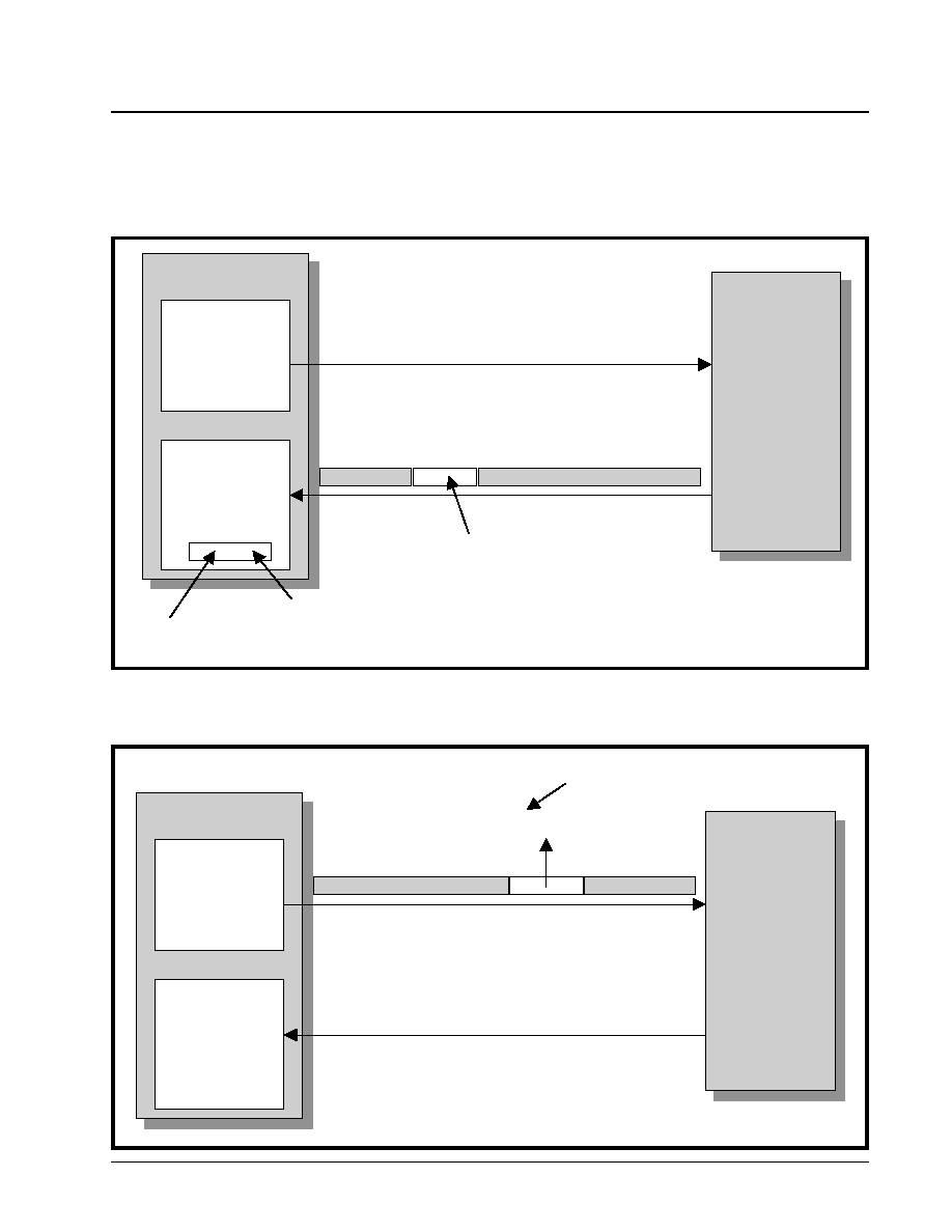
·Á
·Á
·Á
·Á
XRT7250
DS3/E3 FRAMER IC
REV. 1.1.1
401
tion of the Local Transmit E3 Framer block, which will
transmit an E3 frame to the Remote Terminal, with
the FEBE bit-field set to "0" . This signaling indicates
that the Local Receive E3 Framer has received an er-
ror-free E3 frame.
F
IGURE
196. I
LLUSTRATION
OF
THE
L
OCAL
R
ECEIVE
E3 F
RAMER
BLOCK
,
RECEIVING
AN
E3 F
RAME
(
FROM
THE
R
EMOTE
T
ERMINAL
)
WITH
A
CORRECT
EM B
YTE
.
Transmit E3
Framer
Receive E3
Framer
Local Terminal
Remote
Terminal
EM Byte
Locally Calculated
EM Byte
0x5A
0x5A
F
IGURE
197. I
LLUSTRATION
OF
THE
L
OCAL
R
ECEIVE
E3 F
RAMER
BLOCK
,
TRANSMITTING
AN
E3 F
RAME
(
TO
THE
R
EMOTE
T
ERMINAL
)
WITH
THE
FEBE
BIT
(
WITHIN
THE
MA
BYTE
-
FIELD
)
SET
TO
"0"
Transmit E3
Framer
Receive E3
Framer
Local Terminal
Remote
Terminal
MA Byte
x0xxxxxx
FEBE bit
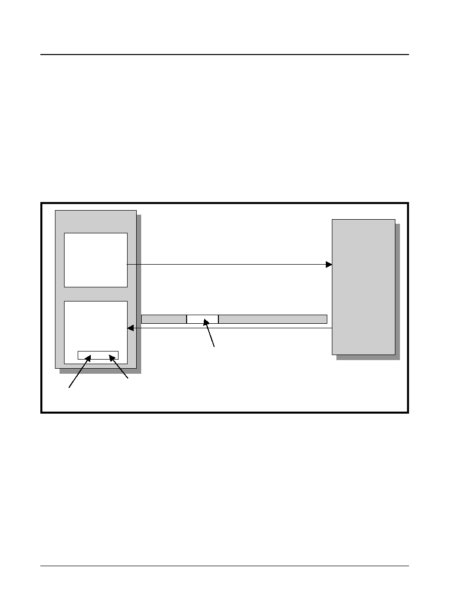
XRT7250
·Á
·Á
·Á
·Á
DS3/E3 FRAMER IC
REV. 1.1.1
402
However, if the locally computed BIP-8 value does not
match the EM byte of the corresponding E3 frame,
then the Receive E3 Framer block will do the follow-
ing.
∑ It will inform the Remote Terminal of this fact by
having the Local Transmit E3 Framer block send the
Remote Terminal an E3 frame, with the FEBE bit-
field, within the MA byte, set to "1". This phenome-
non is illustrated below in Figure 198 and
Figure 199.
Figure 198 illustrates the Local Receive E3 Framer
receiving an errored E3 frame. In this figure, the Lo-
cal Receive E3 Frame block is receiving an E3 frame
with an EM byte containing the value "0x5A". This
value does not match the locally computed EM byte
value of "0x5B". Consequently, there is an error in
this E3 frame.
Figure 199 illustrates the subsequent action of the
Local Transmit E3 Framer block, which will transmit
an E3 frame, with the FEBE bit-field set to "1" to the
Remote Terminal. This signaling indicates that the
Local Receive E3 Framer block has received an er-
rored E3 frame.
F
IGURE
198. I
LLUSTRATION
OF
THE
L
OCAL
R
ECEIVE
E3 F
RAMER
BLOCK
,
RECEIVING
AN
E3 F
RAME
(
FROM
THE
R
EMOTE
T
ERMINAL
)
WITH
AN
INCORRECT
EM B
YTE
.
Transmit E3
Framer
Receive E3
Framer
Local Terminal
Remote
Terminal
EM Byte
Locally Calculated
EM Byte
0x5A
0x5B
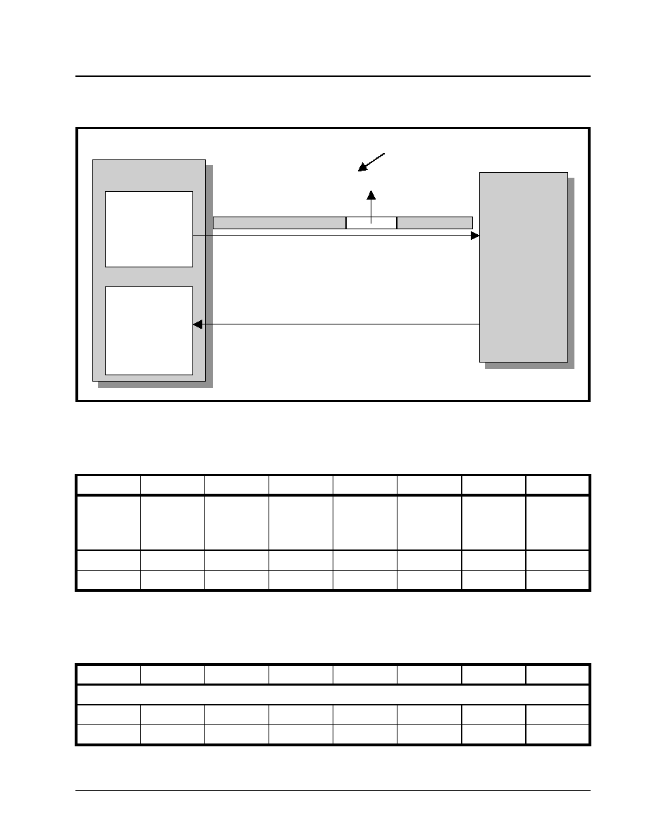
·Á
·Á
·Á
·Á
XRT7250
DS3/E3 FRAMER IC
REV. 1.1.1
403
In additional to the FEBE bit-field signaling, the Re-
ceive E3 Framer block will generate the BIP-8 Error
Interrupt to the Microprocessor. Hence, it will set bit 2
(BIP-8 Error Interrupt Status) to "1", as depicted be-
low.
Finally, the Receive E3 Framer block will increment
the PMON Parity Error Count registers. The byte for-
mat of these registers are presented below.
F
IGURE
199. I
LLUSTRATION
OF
THE
L
OCAL
R
ECEIVE
E3 F
RAMER
BLOCK
,
TRANSMITTING
AN
E3 F
RAME
(
TO
THE
R
EMOTE
T
ERMINAL
)
WITH
THE
FEBE
BIT
(
WITHIN
THE
MA
BYTE
-
FIELD
)
SET
TO
"1"
Transmit E3
Framer
Receive E3
Framer
Local Terminal
Remote
Terminal
MA Byte
x1xxxxxx
FEBE bit
RXE3 INTERRUPT STATUS REGISTER - 2 (ADDRESS = 0X15)
B
IT
7
B
IT
6
B
IT
5
B
IT
4
B
IT
3
B
IT
2
B
IT
1
B
IT
0
Not Used
TTB
Change
Interrupt
Status
Not Used
FEBE
Interrupt
Status
FERF
Interrupt
Status
BIP-8
Error
Interrupt
Status
Framing
Byte Error
Interrupt
Status
RxPld
Mis
Interrupt
Status
RO
RUR
RO
RUR
RUR
RUR
RUR
RUR
0
0
0
0
0
0
0
0
PMON PARITY ERROR COUNT REGISTER - MSB (ADDRESS = 0X54)
B
IT
7
B
IT
6
B
IT
5
B
IT
4
B
IT
3
B
IT
2
B
IT
1
B
IT
0
Parity Error Count - High Byte
RUR
RUR
RUR
RUR
RUR
RUR
RUR
RUR
0
0
0
0
0
0
0
0
XRT7250
·Á
·Á
·Á
·Á
DS3/E3 FRAMER IC
REV. 1.1.1
404
The user can determine the number of BIP-8 Errors
that have been detected by the Receive E3 Framer
block, since the last read of these registers. These
registers are reset-upon-read.
6.3.2.8
Processing of the Far-End-Block Error
(FEBE) Bit-fields
Whenever the Receive E3 Framer detects an error in
the incoming E3 frame, via EM byte verification, it will
inform the Local Transmit E3 Framer of this fact. The
Local Transmit E3 Framer will, in turn, notify the Re-
mote Terminal (e.g., the source of the errored E3
frame) by transmitting an E3 frame, with the FEBE
bit-field (within the MA byte) set to "1".
If the Receive E3 Framer receives any E3 frame, with
the FEBE bit-field set to "1", then it will do the follow-
ing.
∑ It will generate a FEBE Event interrupt to the Micro-
processor/Microcontroller. Hence, the Receive E3
Framer block will set bit 4 (FEBE Interrupt Status)
within the Rx E3 Framer Interrupt Status Register -
2, as depicted below.
∑ Increment the PMON Received FEBE Event Count
register - MSB/LSB, which is located at 0x56 and
0x57 in the Framer Address space. The byte-for-
mat of these registers are presented below.
The user can determine the total number of FEBE
Events (e.g., E3 frames that have been received with
PMON PARITY ERROR COUNT REGISTER - LSB (ADDRESS = 0X55)
B
IT
7
B
IT
6
B
IT
5
B
IT
4
B
IT
3
B
IT
2
B
IT
1
B
IT
0
Parity Error Count - Low Byte
RUR
RUR
RUR
RUR
RUR
RUR
RUR
RUR
0
0
0
0
0
0
0
0
RXE3 INTERRUPT STATUS REGISTER - 2 (ADDRESS = 0X15)
B
IT
7
B
IT
6
B
IT
5
B
IT
4
B
IT
3
B
IT
2
B
IT
1
B
IT
0
Not Used
TTB Change
Interrupt Status
Not Used
FEBE Interrupt
Status
FERF Interrupt
Status
BIP-8 Error
Interrupt Status
Framing Byte
Error Interrupt
Status
RxPld Mis
Interrupt Status
RO
RUR
RO
RUR
RUR
RUR
RUR
RUR
0
0
0
1
0
0
0
0
PMON FEBE EVENT COUNT REGISTER - MSB (ADDRESS = 0X56)
B
IT
7
B
IT
6
B
IT
5
B
IT
4
B
IT
3
B
IT
2
B
IT
1
B
IT
0
FEBE Event Count - High Byte
RUR
RUR
RUR
RUR
RUR
RUR
RUR
RUR
0
0
0
0
0
0
0
0
PMON FEBE EVENT COUNT REGISTER - LSB (ADDRESS = 0X57)
B
IT
7
B
IT
6
B
IT
5
B
IT
4
B
IT
3
B
IT
2
B
IT
1
B
IT
0
FEBE Event Count - Low Byte
RUR
RUR
RUR
RUR
RUR
RUR
RUR
RUR
0
0
0
0
0
0
0
0

·Á
·Á
·Á
·Á
XRT7250
DS3/E3 FRAMER IC
REV. 1.1.1
405
the FEBE bit-field set to "1") that have occurred since
the last read of this register. This register is reset-up-
on-read.
6.3.2.9
Receiving the Trail Trace Buffer Mes-
sages
The XRT7250 Framer IC device contains 16 bytes
worth of Transmit Trail Trace Buffers, and 16 bytes
worth of Receive Trail Trace Buffers, as described be-
low. The role of the Transmit Trail Trace Buffers are
described in Section 5.2.4.2..
The XRT7250 DS3/E3 Framer IC contains 16 Re-
ceive Trail Trace Buffer registers (e.g., RxTTB-0
through RxTTB-15). The purpose of these registers
are to receive and store the incoming Trail Access
Point Identifier from the Remote Transmitting Termi-
nal.
The Local Receiving Terminal will use this information
to verify that it is still receiving data from its intended
transmitter. The specific use of these registers fol-
lows.
For Trail Trace Buffer purposes, the Remote Transmit
E3 Framer block will group 16 consecutive E3 frames
into a Trail Trace Buffer super-frame. When the Re-
mote Transmit E3 Framer is generating the first E3
frame, within a Trail Trace Buffer super-frame, it will
insert the value [1, C6, C5, C4, C3, C2, C1, C0], into
the TR byte-field of this Outbound E3 frame. The re-
maining 15 TR byte-fields (within this Trail Trace Buff-
er super-frame) will consists of ASCII characters that
are required for the E.164 numbering format.
When the Local Receive E3 Framer block receives an
E3 frame, containing a value in the TR byte that has a
"1" in the MSB position, then it (the Receive E3 Fram-
er block) will write this value into the RxTTB-0 Regis-
ter (Address = 0x1C). Once this occurs, the Receive
E3 Framer block will notify the Microprocessor of this
new incoming Trail Trace Buffer message by generat-
ing the Change in Trail Trace Buffer Message inter-
rupt. The Receive E3 Framer block will also set bit 6
(TTB Change Interrupt Status) within the Rx E3
Framer Interrupt Status Register - 2, as depicted be-
low.
The contents of the TR byte-field, in the very next E3
frame will be written into the Rx TTB-1 Register (Ad-
dress = 0x1D), and so on until all 16 bytes have been
received.
N
OTES
:
1. Anytime the Receive E3 Framer block receives an
E3 frame that contains an octet in the TR byte-field,
with a "1" in the MSB (Most Significant Bit) position,
then the Receive E3 Framer block will (1) write the
contents of the TR byte-field (in this E3 frame) into
the RxTTB-0 Register,
2. It will generate the Change in Trail Trace Buffer
Interrupt. The Receive E3 Framer will do these
things independent of the number of E3 frames that
have been received since the last occurrence of the
Change in Trail Trace Buffer Interrupt. Hence, the
user, when writing data into the Tx TTB registers,
must take care to insure that only the Tx TTB-0 reg-
ister contains an octet with a "1" in the MSB posi-
tion. All remaining Tx TTB registers (e.g., TxTTB-1
through TxTTB-15) must contain octets with a "0" in
the MSB position.
3. The Framer IC will not verify the CRC-7 value that
is written into the Rx TTB-0" register. It is up to the
user's system hardware and/or software to perform
this verification.
6.3.3
The Receive HDLC Controller Block
The Receive E3 HDLC Controller block can be used
to receive message-oriented signaling (MOS) type
data link messages from the remote terminal equip-
ment.
The MOS types of HDLC message processing is dis-
cussed in detail below.
The Message Oriented Signaling (e.g., LAP-D)
Processing via the Receive DS3 HDLC Controller
block
The LAPD Receiver (within the Receive E3 HDLC
Controller block) allows the user to receive PMDL
messages from the remote terminal equipment, via
RXE3 INTERRUPT STATUS REGISTER - 2 (ADDRESS = 0X15)
B
IT
7
B
IT
6
B
IT
5
B
IT
4
B
IT
3
B
IT
2
B
IT
1
B
IT
0
Not Used
TTB
Change
Interrupt
Status
Not Used
FEBE
Interrupt
Status
FERF
Interrupt
Status
BIP-8
Error Interrupt
Status
Framing
Byte Error
Interrupt
Status
RxPld
Mis
Interrupt
Status
RO
RUR
RO
RUR
RUR
RUR
RUR
RUR
0
0
0
0
0
0
0
0
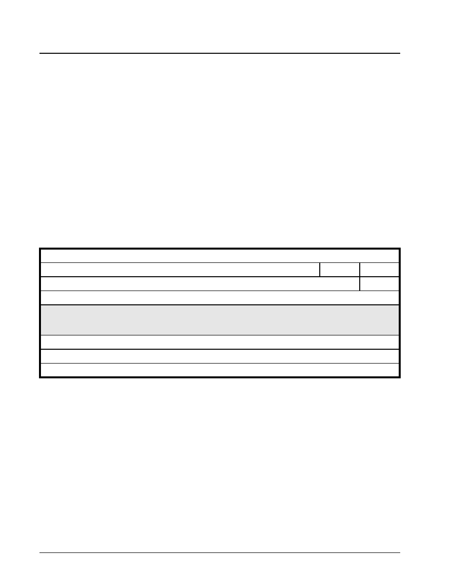
XRT7250
·Á
·Á
·Á
·Á
DS3/E3 FRAMER IC
REV. 1.1.1
406
the Inbound E3 frames. In this case, the Inbound
message bits will be carried by either the "GC" or the
"NR" byte-fields within each E3 Frame. The remote
LAPD Transmitter will transmit a LAPD Message to
the Near-End Receiver via either one of these bytes
within each E3 Frame. The LAPD Receiver will re-
ceive and store the information portion of the re-
ceived LAPD frame into the Receive LAPD Message
Buffer, which is located at addresses: 0xDE through
0x135 within the on-chip RAM. The LAPD Receiver
has the following responsibilities.
∑ Framing to the incoming LAPD Messages
∑ Filtering out stuffed "0's" (within the information
payload)
∑ Storing the Frame Message into the Receive LAPD
Message Buffer
∑ Perform Frame Check Sequence (FCS) Verification
∑ Provide status indicators for
End of Message (EOM)
Flag Sequence Byte detected
Abort Sequence detected
Message Type
C/R Type
The occurrence of FCS Errors
The LAPD receiver's actions are facilitated via the fol-
lowing two registers.
∑ Rx E3 LAPD Control Register
∑ Rx E3 LAPD Status Register
Operation of the LAPD Receiver
The LAPD Receiver, once enabled, will begin search-
ing for the boundaries of the incoming LAPD mes-
sage. The LAPD Message Frame boundaries are de-
lineated via the Flag Sequence octets (0x7E), as de-
picted in Figure 200.
Where: Flag Sequence = 0x7E
SAPI + CR + EA = 0x3C or 0x3E
TEI + EA = 0x01
Control = 0x03
The 16 bit FCS is calculated using CRC-16, x16 +
x12 + x5 + 1
The local µP (at the remote terminal), while assem-
bling the LAPD Message frame, will insert an addi-
tional byte at the beginning of the information (pay-
load) field. This first byte of the information field indi-
cates the type and size of the message being trans-
ferred. The value of this information field and the
corresponding message type/size follow:
CL Path Identification = 0x38 (76 bytes)
IDLE Signal Identification = 0x34 (76 bytes)
Test Signal Identification = 0x32 (76 bytes)
ITU-T Path Identification = 0x3F (82 bytes)
Enabling and Configuring the LAPD Receiver
Before the LAPD Receiver can begin to receive and
process incoming LAPD Message frames, the user
must do two things.
1. The byte-field within each E3 frame which will be
carrying the comprising octets of the LAPD Mes-
sage frame must be specified and
2. The LAPD Receiver must be enabled.
Each of these steps are discussed in detail below.
1. Specifying which byte-field, within each E3 frame,
will be carrying the LAPD Message frame.
The LAPD Receiver can receive the LAPD Message
frame octets via either the GC-byte-field or the NR-
byte-field, within each incoming E3 frame. The user
makes this selection by writing the appropriate bit to
F
IGURE
200. LAPD M
ESSAGE
F
RAME
F
ORMAT
Flag Sequence (8 bits)
SAPI (6-bits)
C/R
EA
TEI (7 bits)
EA
Control (8-bits)
76 or 82 Bytes of Information (Payload)
FCS - MSB
FCS - LSB
Flag Sequence (8-bits)

·Á
·Á
·Á
·Á
XRT7250
DS3/E3 FRAMER IC
REV. 1.1.1
407
Bit 1 (DL from NR) within the Rx E3 LAPD Control
Register, as depicted below.
Writing a "0" into this bit-field causes the LAPD Re-
ceiver to read in the octets from the GC byte-field of
each E3 frame and with these octets, reassembling
the LAPD Message frame. Writing a "1" into this bit-
field causes the LAPD Receiver to receive the LAPD
Message frame octets from the NR byte-field of each
E3 frame.
2. Enabling the LAPD Receiver
The LAPD Receiver must be enabled before it can
begin receiving and processing any LAPD Message
frames. The LAPD Receiver can be enabled by writ-
ing a "1" to Bit 2 (RxLAPD Enable) of the Rx E3 LAPD
Control Register, as indicated below.
Once the LAPD Receiver has been enabled, it will be-
gin searching for the Flag Sequence octet (0x7E), in
either the "GC" or the "NR" byte-fields within each in-
coming E3 frame. When the LAPD Receiver finds the
flag sequence byte, it will assert the Flag Present bit
(Bit 0) within the Rx E3 LAPD Status Register, as de-
picted below.
The receipt of the Flag Sequence octet can mean
one of two things.
1. This Flag Sequence byte may be marking the
beginning or end of an incoming LAPD Message
frame.
2. The Received Flag Sequence octet could be just
one of many Flag Sequence octets that are trans-
mitted via the E3 Transport Medium, during idle
periods between the transmission of LAPD Mes-
sage frames.
The LAPD Receiver will negate the Flag Present bit
as soon as it has received an octet that is something
other than the Flag Sequence octet. Once this hap-
pens, the LAPD Receiver should be receiving either
octet # 2 of the incoming LAPD Message, or an
ABORT Sequence (e.g., a string of seven or more
consecutive "1's"). If this next set of data is an
RXE3 LAPD CONTROL REGISTER (ADDRESS = 0X18)
B
IT
7
B
IT
6
B
IT
5
B
IT
4
B
IT
3
B
IT
2
B
IT
1
B
IT
0
Not Used
DL from NR
RxLAPD
Enable
RxLAPD
Interrupt
Enable
RxLAPD
Interrupt
Status
RO
RO
RO
RO
R/W
R/W
R/W
RUR
0
0
0
0
0
0
1
0
RXE3 LAPD CONTROL REGISTER (ADDRESS = 0X18)
B
IT
7
B
IT
6
B
IT
5
B
IT
4
B
IT
3
B
IT
2
B
IT
1
B
IT
0
Not Used
DL from NR
RxLAPD
Enable
RxLAPD
Interrupt
Enable
RxLAPD
Interrupt
Status
RO
RO
RO
RO
R/W
R/W
R/W
RUR
0
0
0
0
0
1
1
0
RXE3 LAPD STATUS REGISTER (ADDRESS = 0X19)
B
IT
7
B
IT
6
B
IT
5
B
IT
4
B
IT
3
B
IT
2
B
IT
1
B
IT
0
Not Used
Rx ABORT
RxLAPDType[1:0]
RxCR
Type
RxFCS
Error
End of
Message
Flag
Present
RO
RO
RO
RO
RO
RO
RO
RO
0
0
0
0
0
0
0
1

XRT7250
·Á
·Á
·Á
·Á
DS3/E3 FRAMER IC
REV. 1.1.1
408
ABORT Sequence, then the LAPD Receiver will as-
sert the RxABORT bit-field (Bit 6) within the Rx E3
LAPD Status Register, as depicted below.
However, if this next octet is Octet #2 of an incoming
LAPD Message frame, then the LAPD Receiver is be-
ginning to receive a LAPD Message frame.
As the LAPD Receiver receives this LAPD Message
frame, it is reading in the LAPD Message frame oc-
tets, from either the "GC" or the "NR" byte-fields with-
in each incoming E3 frame. Secondly, it is reassem-
bling these octets into a LAPD Message frame.
Once the LAPD Receiver has received the complete
LAPD Message frame, then it will proceed to perform
the following five (5) steps.
1. PMDL Message Extraction
The LAPD Receiver will extract out the PMDL Mes-
sage, from the newly received LAPD Message frame.
The LAPD Receiver will then write this PMDL Mes-
sage into the Receive LAPD Message buffer within
the Framer IC.
N
OTE
: As the LAPD Receiver is extracting the PMDL Mes-
sage, from the newly received LAPD Message frame, the
LAPD Receiver will also check the PMDL data for the
occurrence of stuff bits (e.g., "0s" that were inserted into the
PMDL Message by the Remote LAPD Transmitter, in order
to prevent this data from mimicking the Flag Sequence byte
or an ABORT Sequence), and remove them prior to writing
the PMDL Message into the Receive LAPD Message
Buffer. Specifically, the LAPD Receiver will search through
the PMDL Message data and will remove any "0" that
immediately follows a string of 5 consecutive "1's".
For more information on how the LAPD Transmitter
inserted these stuff bits, please see Section 5.2.3.1.
2. FCS (Frame Check Sequence) Word Verification
The LAPD Receiver will compute the CRC-16 value
of the header octets and the PMDL Message octets,
within this LAPD Message frame and will compare it
with the value of the two octets, residing in the FCS
word-field of this LAPD Message frame. If the FCS
value of the newly received LAPD Message frame
matches the locally-computed CRC-16 value, then
the LAPD Receiver will conclude that it has received
this LAPD Message frame in an error-free manner.
However, if the FCS value does not match the locally-
computed CRC-16 value, then the LAPD Receiver
will conclude that this LAPD Message frame is erred.
The LAPD Receiver will indicate the results of this
FCS Verification process by setting Bit 2 (RxFCS Er-
ror) within the Rx E3 LAPD Status Register, to the ap-
propriate value as tabulated below.
If the LAPD Receiver detects an error in the FCS val-
ue, then it will set the RxFCS Error bit-field to "1".
Conversely, if the LAPD Receiver does not detect an
error in the FCS value, the it will clear the RxFCS Er-
ror bit-field to "0".
N
OTE
: The LAPD Receiver will extract and write the PMDL
Message into the Receive LAPD Message buffer indepen-
dent of the results of FCS Verification. Hence, the user is
urged to validate each PMDL Message that is read in from
the Receive LAPD Message buffer, by first checking the
state of this bit-field.
3. Check and Report the State of the "C/R" Bit-field
RXE3 LAPD STATUS REGISTER (ADDRESS = 0X19)
B
IT
7
B
IT
6
B
IT
5
B
IT
4
B
IT
3
B
IT
2
B
IT
1
B
IT
0
Not Used
Rx ABORT
RxLAPDType[1:0]
RxCR
Type
RxFCS
Error
End of
Message
Flag
Present
RO
RO
RO
RO
RO
RO
RO
RO
0
1
0
0
0
0
0
0
RXE3 LAPD STATUS REGISTER (ADDRESS = 0X19)
B
IT
7
B
IT
6
B
IT
5
B
IT
4
B
IT
3
B
IT
2
B
IT
1
B
IT
0
Not Used
Rx ABORT
RxLAPDType[1:0]
RxCR
Type
RxFCS
Error
End of
Message
Flag
Present
RO
RO
RO
RO
RO
RO
RO
RO
0
0
0
0
0
1
0
0
·Á
·Á
·Á
·Á
XRT7250
DS3/E3 FRAMER IC
REV. 1.1.1
409
After receiving the LAPD Message frame, the LAPD
Receiver will check the state of the "C/R" bit-field,
within octet # 2 of the LAPD Message frame header
and will reflect this value in Bit 3 (Rx CR Type) within
the Rx E3 LAPD Status Register, as depicted below.
When this bit-field is "0", it means that this LAPD
Message frame is originating from a customer instal-
lation. When this bit-field is "1", it means that this
LAPD Message frame is originating from a network
terminal.
4. Identify the Type of LAPD Message Frame/PMDL
Message
Next, the LAPD Receiver will check the value of the
first octet within the PMDL Message field, of the
LAPD Message frame. Recall that from Section _,
that when operating the LAPD Transmitter, the user is
required to write in a byte of a specific value into the
first octet position within the Transmit LAPD Message
buffer. The value of this byte corresponds to the type
of LAPD Message frame/PMDL Message that is to be
transmitted to the Remote LAPD Receiver. This Mes-
sage-Type Identification octet is transported to the
Remote LAPD Receiver, along with the rest of the
LAPD frame. From this Message Type Identification
octet, the LAPD Receiver will know the type of size of
the newly received PMDL Message. The LAPD Re-
ceiver will then reflect this information in Bits 4 and 5
(RxLAPDType[1:0]) within the Rx E3 LAPD Status
Register, as depicted below.
Table 86 presents the relationship between the con-
tents of RxLAPDType[1:0] and the type of message
received by the LAPD Receiver.
N
OTE
: Prior to reading in the PMDL Message from the
Receive LAPD Message buffer, the user is urged to read
the state of the RxLAPDType[1:0] bit-fields in order to deter-
mine the size of this message.
5. Inform the Local Microprocessor/External Cir-
cuitry of the receipt of the new LAPD Message
frame.
RXE3 LAPD STATUS REGISTER (ADDRESS = 0X19)
B
IT
7
B
IT
6
B
IT
5
B
IT
4
B
IT
3
B
IT
2
B
IT
1
B
IT
0
Not Used
Rx ABORT
RxLAPDType[1:0]
RxCR
Type
RxFCS
Error
End of
Message
Flag
Present
RO
RO
RO
RO
RO
RO
RO
RO
0
0
0
0
1
0
0
0
RXE3 LAPD STATUS REGISTER (ADDRESS = 0X19)
B
IT
7
B
IT
6
B
IT
5
B
IT
4
B
IT
3
B
IT
2
B
IT
1
B
IT
0
Not Used
Rx ABORT
RxLAPDType[1:0]
RxCR
Type
RxFCS
Error
End of
Message
Flag
Present
RO
RO
RO
RO
RO
RO
RO
RO
0
0
0
0
0
0
0
0
T
ABLE
86: T
HE
R
ELATIONSHIP
BETWEEN
THE
C
ONTENTS
OF
R
X
LAPDT
YPE
[1:0]
BIT
-
FIELDS
AND
THE
PMDL
M
ESSAGE
T
YPE
/S
IZE
R
X
LAPDT
YPE
[1:0]
PMDL M
ESSAGE
T
YPE
PMDL M
ESSAGE
S
IZE
00
Test Signal Identification
76 Bytes
01
Idle Signal Identification
76 Bytes
10
CL Path Identification
76 Bytes
11
ITU-T Path Identification
82 Bytes

XRT7250
·Á
·Á
·Á
·Á
DS3/E3 FRAMER IC
REV. 1.1.1
410
Finally, after the LAPD Receiver has received and
processed the newly received LAPD Message frame
(per steps 1 through 4, as described above), it will in-
form the local Microprocessor that a LAPD Message
frame has been received and is ready for user-sys-
tem handling. The LAPD Receiver will inform the Mi-
croprocessor/Microcontroller and the external circuit-
ry by:
∑ Generating a LAPD Message Frame Received
interrupt to the Microprocessor. The purpose of
this interrupt is to let the Microprocessor know that
the Receive LAPD Message buffer contains a new
PMDL Message that needs to be read and pro-
cessed. When the LAPD Receiver generates this
interrupt, it will set bit 0 (RxLAPD Interrupt Status)
within the Rx E3 LAPD Control Register to "1" as
depicted below.
∑ Setting Bit 1 (End of Message) within the Rx E3
LAPD Status Register, to "1" as depicted below.
In summary, Figure 201 presents a flow chart depict-
ing how the LAPD Receiver functions.
RXE3 LAPD CONTROL REGISTER (ADDRESS = 0X18)
B
IT
7
B
IT
6
B
IT
5
B
IT
4
B
IT
3
B
IT
2
B
IT
1
B
IT
0
Not Used
DL from NR
RxLAPD
Enable
RxLAPD
Interrupt
Enable
RxLAPD
Interrupt
Status
RO
RO
RO
RO
R/W
R/W
R/W
RUR
0
0
0
0
0
0
0
1
RXE3 LAPD STATUS REGISTER (ADDRESS = 0X19)
B
IT
7
B
IT
6
B
IT
5
B
IT
4
B
IT
3
B
IT
2
B
IT
1
B
IT
0
Not Used
Rx ABORT
RxLAPDType[1:0]
RxCR
Type
RxFCS
Error
End of
Message
Flag
Present
RO
RO
RO
RO
RO
RO
RO
RO
0
0
0
0
0
0
1
0
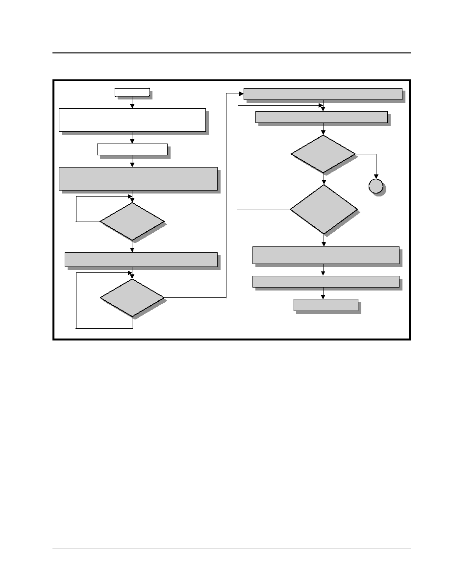
·Á
·Á
·Á
·Á
XRT7250
DS3/E3 FRAMER IC
REV. 1.1.1
411
F
IGURE
201. F
LOW
C
HART
DEPICTING
THE
F
UNCTIONALITY
OF
THE
LAPD R
ECEIVER
START
Indicate whether the LAPD Receiver should retrieve the
LAPD Message frame octets from the NR or GC byte-field,
within each incoming E3 Frame.
Enable the LAPD Receiver
The LAPD Receiver will begin searching for the Flag Sequence
octet (0x7E) in the "selected" byte-field (e.g., NR or GC) of each
incoming E3 frame.
Is
Flag Sequence
octet
Present?
Assert the "Flag Present" bit-field within the "Rx E3 LAPD
Status Register (Address = 0x19).
Is
non-Flag Sequence
octet detected
?
Set the "RxLAPDType[1:0] bit-fields to the appropriate value.
Continue to read in the LAPD Message frame octets
Is
Abort Sequence
Detected?
Has
the last byte
of the LAPD Message
frame been
received?
Set the "End Of Message" bit-field within the "RxE3
LAPD Status Register (Address = 0x19)
Unstuff the "PMDL" portion of the LAPD Message frame.
Goto Figure 185
No
A
Yes
No
Yes
No
Yes
No
Yes
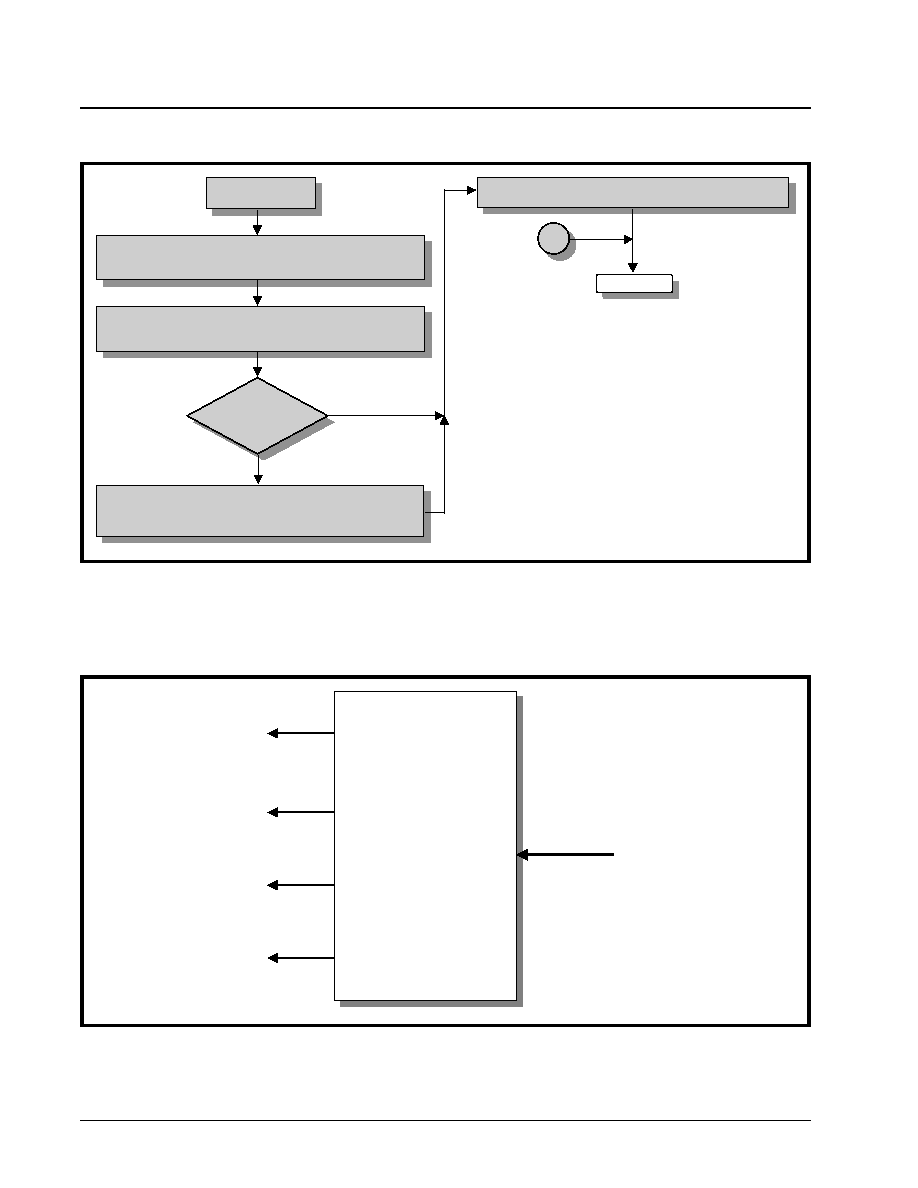
XRT7250
·Á
·Á
·Á
·Á
DS3/E3 FRAMER IC
REV. 1.1.1
412
6.3.4
The Receive Overhead Data Output Inter-
face
Figure 203 presents a simple illustration of the Re-
ceive Overhead Data Output Interface block within
the XRT7250.
The E3, ITU-T G.832 frame consists of 537 bytes. Of
these bytes, 530 bytes are payload bits and the re-
maining 7 bytes are overhead bytes. The XRT7250
has been designed to handle and process both the
payload type and overhead type bytes for each E3
frame.
F
IGURE
202. F
LOW
C
HART
DEPICTING
THE
F
UNCTIONALITY
OF
THE
LAPD R
ECEIVER
(C
ONTINUED
)
Compute "Frame Check Sequence (FCS)" value of incoming
LAPD Message Frame.
Compare "locally-computed" FCS value with that contained
within the newly received LAPD Message frames.
Do the
two FCS values
Match?
FCS Error Detected
Assert the "Rx FCS Error" bit-field within the "Rx E3
LAPD Status Register (Address = 0x19).
Generate the "Receive LAPD Message frame" interrupt.
From Figure 184
End
A
No
Yes
F
IGURE
203. A S
IMPLE
I
LLUSTRATION
OF
THE
R
ECEIVE
O
VERHEAD
O
UTPUT
I
NTERFACE
BLOCK
Receive Overhead
Output Interface
Block
Receive Overhead
Output Interface
Block
From Receive
E3 Framer Block
RxOHFrame
RxOH
RxOHClk
RxOHEnable

·Á
·Á
·Á
·Á
XRT7250
DS3/E3 FRAMER IC
REV. 1.1.1
413
Within the Receive Section of the XRT7250, the Re-
ceive Payload Data Output Interface block has been
designed to handle the payload bits. Likewise, the
Receive Overhead Data Output Interface block has
been designed to handle and process the overhead
bits.
The Receive Overhead Data Output Interface block
unconditionally outputs the contents of all overhead
bits. The XRT7250 does not offer the user a means
to shut off this transmission of data. However, the
Receive Overhead Output Interface block does pro-
vide the user with the appropriate output signals for
external Data Link Layer equipment to sample and
process these overhead bits, via the following two
methods.
∑ Method 1- Using the RxOHClk clock signal.
∑ Method 2 - Using the RxClk and RxOHEnable out-
put signals.
Each of these methods are described below.
6.3.4.1
Method 1 - Using the RxOHClk Clock
signal
The Receive Overhead Data Output Interface block
consists of four (4) signals. Of these four signals, the
following three signals are to be used when sampling
the E3 overhead bits via Method 1.
∑ RxOH
∑ RxOHClk
∑ RxOHFrame
Each of these signals are listed and described below
in Table 87.
Interfacing the Receive Overhead Data Output In-
terface block to the Terminal Equipment (Method
1)
Figure 204 illustrates how one should interface the
Receive Overhead Data Output Interface block to the
Terminal Equipment when using Method 1, to sample
and process the overhead bits from the Inbound E3
data stream.
Method 1 Operation of the Terminal Equipment
If the Terminal Equipment intends to sample any
overhead data from the Inbound E3 data stream (via
the Receive Overhead Data Output Interface block)
then it is expected to do the following:
F
IGURE
204. I
LLUSTRATION
OF
HOW
TO
INTERFACE
THE
T
ERMINAL
E
QUIPMENT
TO
THE
R
ECEIVE
O
VERHEAD
D
ATA
O
UTPUT
I
NTERFACE
BLOCK
(
FOR
M
ETHOD
1).
Terminal Equipment
XRT7250 E3 Framer IC
RxOHClk
E3_OH_Clock_In
RxOH
RxOHFrame
E3_OH_In
Rx_Start_of_Frame

XRT7250
·Á
·Á
·Á
·Á
DS3/E3 FRAMER IC
REV. 1.1.1
414
1. Sample the state of the RxOHFrame signal (e.g.,
the Rx_Start_of_Frame input signal) on the rising
edge of the RxOHClk (e.g., the
E3_OH_Clock_In) signal.
2. Keep track of the number of rising clock edges
that have occurred in the RxOHClk (e.g., the
E3_OH_Clock_In) signal, since the last time the
RxOHFrame signal was sampled "High". By
doing this, the Terminal Equipment will be able to
keep track of which overhead byte is being output
via the RxOH output pin. Based upon this infor-
mation, the Terminal Equipment will be able to
derive some meaning from these overhead bits.
Table 88 relates the number of rising clock edges (in
the RxOHClk signal, since the RxOHFrame signal
was last sampled "High") to the E3 Overhead bit that
is being output via the RxOH output pin.
T
ABLE
87: L
ISTING
AND
D
ESCRIPTION
OF
THE
P
IN
A
SSOCIATED
WITH
THE
R
ECEIVE
O
VERHEAD
D
ATA
O
UTPUT
I
NTERFACE
B
LOCK
S
IGNAL
N
AME
T
YPE
D
ESCRIPTION
RxOH
Output
Receive Overhead Data Output pin:
The XRT7250 will output the overhead bits, within the incoming E3 frames, via this pin.
The Receive Overhead Data Output Interface block will output a given overhead bit, upon the
falling edge of RxOHClk. Hence, the external data link equipment should sample the data, at
this pin, upon the rising edge of RxOHClk.
The XRT7250 will always output the E3 Overhead bits via this output pin. There are no exter-
nal input pins or register bit settings available that will disable this output pin.
RxOHClk
Output
Receive Overhead Data Output Interface Clock Signal:
The XRT7250 will output the Overhead bits (within the incoming E3 frames), via the RxOH out-
put pin, upon the falling edge of this clock signal.
As a consequence, the user's data link equipment should use the rising edge of this clock sig-
nal to sample the data on both the RxOH and RxOHFrame output pins.
This clock signal is always active.
RxOHFrame
Output
Receive Overhead Data Output Interface - Start of Frame Indicator:
The XRT7250 will drive this output pin "High" (for one period of the RxOHClk signal), whenever
the first overhead bit within a given E3 frame is being driven onto the RxOH output pin.
T
ABLE
88: T
HE
R
ELATIONSHIP
BETWEEN
THE
N
UMBER
OF
R
ISING
C
LOCK
E
DGES
IN
R
X
OHC
LK
, (
SINCE
R
X
OHF
RAME
WAS
LAST
SAMPLED
"H
IGH
")
TO
THE
E3 O
VERHEAD
B
IT
,
THAT
IS
BEING
OUTPUT
VIA
THE
R
X
OH
OUTPUT
PIN
N
UMBER
OF
R
ISING
C
LOCK
E
DGES
IN
R
X
OHC
LK
T
HE
O
VERHEAD
B
IT
BEING
OUTPUT
BY
THE
XRT7250
0 (Clock edge is coincident with RxOHFrame being detected "High")
FA1 Byte - Bit 7
1
FA1 Byte - Bit 6
2
FA1 Byte - Bit 5
3
FA1 Byte - Bit 4
4
FA1 Byte - Bit 3
5
FA1 Byte - Bit 2
6
FA1 Byte - Bit 1
7
FA1 Byte - Bit 0
8
FA2 Byte - Bit 7
9
FA2 Byte - Bit 6
10
FA2 Byte - Bit 5

·Á
·Á
·Á
·Á
XRT7250
DS3/E3 FRAMER IC
REV. 1.1.1
415
11
FA2 Byte - Bit 4
12
FA2 Byte - Bit 3
13
FA2 Byte - Bit 2
14
FA2 Byte - Bit 1
15
FA2 Byte - Bit 0
16
EM Byte - Bit 7
17
EM Byte - Bit 6
18
EM Byte - Bit 5
19
EM Byte - Bit 4
20
EM Byte - Bit 3
21
EM Byte - Bit 2
22
EM Byte - Bit 1
23
EM Byte - Bit 0
24
TR Byte - Bit 7
25
TR Byte - Bit 6
26
TR Byte - Bit 5
27
TR Byte - Bit 4
28
TR Byte - Bit 3
29
TR Byte - Bit 2
30
TR Byte - Bit 1
31
TR Byte - Bit 0
32
MA Byte - Bit 7
33
MA Byte - Bit 6
34
MA Byte - Bit 5
35
MA Byte - Bit 4
36
MA Byte - Bit 3
37
MA Byte - Bit 2
38
MA Byte - Bit 1
39
MA Byte - Bit 0
40
NR Byte - Bit 7
T
ABLE
88: T
HE
R
ELATIONSHIP
BETWEEN
THE
N
UMBER
OF
R
ISING
C
LOCK
E
DGES
IN
R
X
OHC
LK
, (
SINCE
R
X
OHF
RAME
WAS
LAST
SAMPLED
"H
IGH
")
TO
THE
E3 O
VERHEAD
B
IT
,
THAT
IS
BEING
OUTPUT
VIA
THE
R
X
OH
OUTPUT
PIN
N
UMBER
OF
R
ISING
C
LOCK
E
DGES
IN
R
X
OHC
LK
T
HE
O
VERHEAD
B
IT
BEING
OUTPUT
BY
THE
XRT7250

XRT7250
·Á
·Á
·Á
·Á
DS3/E3 FRAMER IC
REV. 1.1.1
416
Figure 205 presents the typical behavior of the Re-
ceive Overhead Data Output Interface block, when
Method 1 is being used to sample the incoming E3
overhead bits.
41
NR Byte - Bit 6
42
NR Byte - Bit 5
43
NR Byte - Bit 4
44
NR Byte - Bit 3
45
NR Byte - Bit 2
46
NR Byte - Bit 1
47
NR Byte - Bit 0
48
GC Byte - Bit 7
49
GC Byte - Bit 6
50
GC Byte - Bit 5
51
GC Byte - Bit 4
52
GC Byte - Bit 3
53
GC Byte - Bit 2
54
GC Byte - Bit 1
55
GC Byte - Bit 0
T
ABLE
88: T
HE
R
ELATIONSHIP
BETWEEN
THE
N
UMBER
OF
R
ISING
C
LOCK
E
DGES
IN
R
X
OHC
LK
, (
SINCE
R
X
OHF
RAME
WAS
LAST
SAMPLED
"H
IGH
")
TO
THE
E3 O
VERHEAD
B
IT
,
THAT
IS
BEING
OUTPUT
VIA
THE
R
X
OH
OUTPUT
PIN
N
UMBER
OF
R
ISING
C
LOCK
E
DGES
IN
R
X
OHC
LK
T
HE
O
VERHEAD
B
IT
BEING
OUTPUT
BY
THE
XRT7250
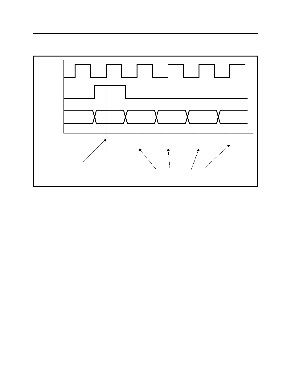
·Á
·Á
·Á
·Á
XRT7250
DS3/E3 FRAMER IC
REV. 1.1.1
417
6.3.4.2
Method 2 - Using RxOutClk and the
RxOHEnable signals
Method 1 requires that the Terminal Equipment be
able to handle an additional clock signal, RxOHClk.
However, there may be a situation in which the Termi-
nal Equipment circuitry does not have the means to
deal with this extra clock signal, in order to use the
Receive Overhead Data Output Interface. Method 2
involves the use of the following signals.
∑ RxOH
∑ RxOutClk
∑ RxOHEnable
∑ RxOHFrame
Each of these signals are listed and described in
Table 89.
F
IGURE
205. I
LLUSTRATION
OF
THE
SIGNALS
THAT
ARE
OUTPUT
VIA
THE
R
ECEIVE
O
VERHEAD
O
UTPUT
I
NTERFACE
(
FOR
M
ETHOD
1).
RxOHClk
RxOHFrame
RxOH
FA1, Bit 7 FA1, Bit 6 FA1, Bit 5 FA1, Bit 4 FA1, Bit 3
Terminal Equipment should sample
the "RxOHFrame" and "RxOH" signals
here.
Recommended Sampling Edges

XRT7250
·Á
·Á
·Á
·Á
DS3/E3 FRAMER IC
REV. 1.1.1
418
Interfacing the Receive Overhead Data Output In-
terface block to the Terminal Equipment (Method
2)
Figure 206 illustrates how one should interface the
Receive Overhead Data Output Interface block to the
Terminal Equipment, when using Method 2 to sample
and process the overhead bits from the Inbound E3
data stream.
T
ABLE
89: L
ISTING
AND
D
ESCRIPTION
OF
THE
P
IN
A
SSOCIATED
WITH
THE
R
ECEIVE
O
VERHEAD
D
ATA
O
UTPUT
I
NTERFACE
B
LOCK
(M
ETHOD
2)
S
IGNAL
N
AME
T
YPE
D
ESCRIPTION
RxOH
Output
Receive Overhead Data Output pin:
The XRT7250 will output the overhead bits, within the incoming E3 frames, via this pin.
The Receive Overhead Output Interface will pulse the RxOHEnable output pin (for one RxOut-
Clk period) at approximately the middle of the RxOH bit period. The user is advised to design
the Terminal Equipment to latch the contents of the RxOH output pin, whenever the RxOHEn-
able output pin is sampled "High" on the falling edge of RxOutClk.
RxOHEnable
Output
Receive Overhead Data Output Enable - Output pin:
The XRT7250 will assert this output signal for one RxOutClk period when it is safe for the Ter-
minal Equipment to sample the data on the RxOH output pin.
RxOHFrame
Output
Receive Overhead Data Output Interface - Start of Frame Indicator:
The XRT7250 will drive this output pin "High" (for one period of the RxOH signal), whenever
the first overhead bit, within a given E3 frame is being driven onto the RxOH output pin.
RxOutClk
Output
Receive Section Output Clock Signal:
This clock signal is derived from the RxLineClk signal (from the LIU) for loop-timing applica-
tions, and the TxInClk signal (from a local oscillator) for local-timing applications. For E3 appli-
cations, this clock signal will operate at 34.368MHz.
The user is advised to design the Terminal Equipment to latch the contents of the RxOH pin,
anytime the RxOHEnable output signal is sampled "High" on the falling edge of this clock sig-
nal.

·Á
·Á
·Á
·Á
XRT7250
DS3/E3 FRAMER IC
REV. 1.1.1
419
Method 2 Operation of the Terminal Equipment
If the Terminal Equipment intends to sample any
overhead data from the Inbound E3 data stream (via
the Receive Overhead Data Output Interface), then it
is expected to do the following.
1. Sample the state of the RxOHFrame signal (e.g.,
the Rx_Start_of_Frame input) on the falling edge
of the RxOutClk clock signal, whenever the RxO-
HEnable output signal is also sampled "High".
2. Keep track of the number of times that the RxO-
HEnable signal has been sampled "High" since
the last time the RxOHFrame was also sampled
"High". By doing this, the Terminal Equipment will
be able to keep track of which overhead bit is
being output via the RxOH output pin. Based
upon this information, the Terminal Equipment
will be able to derive some meaning from these
overhead bits.
3. Table 90 relates the number of RxOHEnable out-
put pulses (that have occurred since both the
RxOHFrame and the RxOHEnable pins were
both sampled "High") to the E3 overhead bit that
is being output via the RxOH output pin.
F
IGURE
206. I
LLUSTRATION
OF
HOW
TO
INTERFACE
THE
T
ERMINAL
E
QUIPMENT
TO
THE
R
ECEIVE
O
VERHEAD
D
ATA
O
UTPUT
I
NTERFACE
BLOCK
(
FOR
M
ETHOD
2).
RxOH
RxOHEnable
RxOutClk
RxOHFrame
E3_OH_In
E3_OH_Enable_In
E3_Clk_In
Rx_Start_of_Frame
Terminal Equipment
XRT7250 E3 Framer IC

XRT7250
·Á
·Á
·Á
·Á
DS3/E3 FRAMER IC
REV. 1.1.1
420
T
ABLE
90: T
HE
R
ELATIONSHIP
BETWEEN
THE
N
UMBER
OF
R
X
OHE
NABLE
OUTPUT
PULSES
(
SINCE
R
X
OHF
RAME
WAS
LAST
SAMPLED
"H
IGH
")
TO
THE
E3 O
VERHEAD
B
IT
,
THAT
IS
BEING
OUTPUT
VIA
THE
R
X
OH
OUTPUT
PIN
N
UMBER
OF
R
X
OHE
NABLE
O
UTPUT
P
ULSES
T
HE
O
VERHEAD
B
IT
BEING
OUTPUT
BY
THE
XRT7250
0 (Clock edge is coincident with RxOHFrame being detected "High")
FA1 Byte - Bit 7
1
FA1 Byte - Bit 6
2
FA1 Byte - Bit 5
3
FA1 Byte - Bit 4
4
FA1 Byte - Bit 3
5
FA1 Byte - Bit 2
6
FA1 Byte - Bit 1
7
FA1 Byte - Bit 0
8
FA2 Byte - Bit 7
9
FA2 Byte - Bit 6
10
FA2 Byte - Bit 5
11
FA2 Byte - Bit 4
12
FA2 Byte - Bit 3
13
FA2 Byte - Bit 2
14
FA2 Byte - Bit 1
15
FA2 Byte - Bit 0
16
EM Byte - Bit 7
17
EM Byte - Bit 6
18
EM Byte - Bit 5
19
EM Byte - Bit 4
20
EM Byte - Bit 3
21
EM Byte - Bit 2
22
EM Byte - Bit 1
23
EM Byte - Bit 0
24
TR Byte - Bit 7
25
TR Byte - Bit 6
26
TR Byte - Bit 5
27
TR Byte - Bit 4
28
TR Byte - Bit 3
29
TR Byte - Bit 2

·Á
·Á
·Á
·Á
XRT7250
DS3/E3 FRAMER IC
REV. 1.1.1
421
Figure 207 presents the typical behavior of the Re-
ceive Overhead Data Output Interface block, when
Method 2 is being used to sample the incoming E3
overhead bits.
30
TR Byte - Bit 1
31
TR Byte - Bit 0
32
MA Byte - Bit 7
33
MA Byte - Bit 6
34
MA Byte - Bit 5
35
MA Byte - Bit 4
36
MA Byte - Bit 3
37
MA Byte - Bit 2
38
MA Byte - Bit 1
39
MA Byte - Bit 0
40
NR Byte - Bit 7
41
NR Byte - Bit 6
42
NR Byte - Bit 5
43
NR Byte - Bit 4
44
NR Byte - Bit 3
45
NR Byte - Bit 2
46
NR Byte - Bit 1
47
NR Byte - Bit 0
48
GC Byte - Bit 7
49
GC Byte - Bit 6
50
GC Byte - Bit 5
51
GC Byte - Bit 4
52
GC Byte - Bit 3
53
GC Byte - Bit 2
54
GC Byte - Bit 1
55
GC Byte - Bit 0
T
ABLE
90: T
HE
R
ELATIONSHIP
BETWEEN
THE
N
UMBER
OF
R
X
OHE
NABLE
OUTPUT
PULSES
(
SINCE
R
X
OHF
RAME
WAS
LAST
SAMPLED
"H
IGH
")
TO
THE
E3 O
VERHEAD
B
IT
,
THAT
IS
BEING
OUTPUT
VIA
THE
R
X
OH
OUTPUT
PIN
N
UMBER
OF
R
X
OHE
NABLE
O
UTPUT
P
ULSES
T
HE
O
VERHEAD
B
IT
BEING
OUTPUT
BY
THE
XRT7250
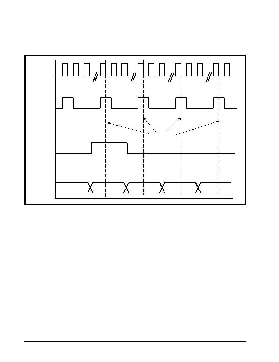
XRT7250
·Á
·Á
·Á
·Á
DS3/E3 FRAMER IC
REV. 1.1.1
422
6.3.5
The Receive Payload Data Output Inter-
face
Figure 208presents a simple illustration of the Re-
ceive Payload Data Output Interface block.
F
IGURE
207. I
LLUSTRATION
OF
THE
SIGNALS
THAT
ARE
OUTPUT
VIA
THE
R
ECEIVE
O
VERHEAD
D
ATA
O
UTPUT
I
NTER
-
FACE
BLOCK
(
FOR
M
ETHOD
2).
RxOutClk
RxOHEnable
RxOHFrame
RxOH
Payload Bit 4239 FA1, Bit 7 FA1, Bit 6 FA1, Bit 5 FA1, Bit 4
Recommended
Sampling
Edges
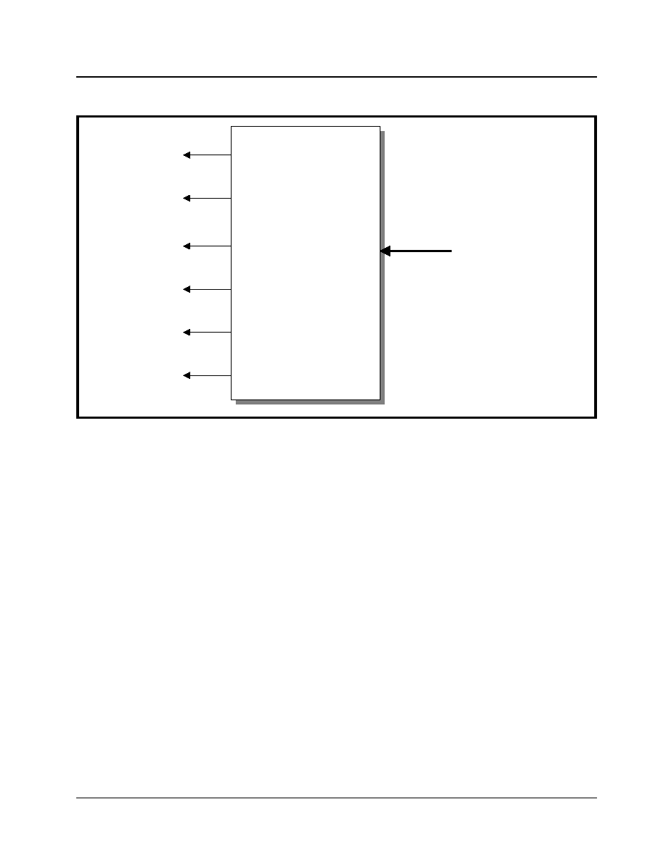
·Á
·Á
·Á
·Á
XRT7250
DS3/E3 FRAMER IC
REV. 1.1.1
423
Each of the output pins of the Receive Payload Data
Output Interface block are listed in Table 91 and de-
scribed below. The exact role that each of these out-
put pins assume, for a variety of operating scenarios
are described throughout this section.
F
IGURE
208. A S
IMPLE
ILLUSTRATION
OF
THE
R
ECEIVE
P
AYLOAD
D
ATA
O
UTPUT
I
NTERFACE
BLOCK
Receive Payload
Data Output
Interface
Receive Payload
Data Output
Interface
RxOHInd
RxSer
RxNib[3:0]
RxClk
RxOutClk
RxFrame
From Receive E3
Framer Block

XRT7250
·Á
·Á
·Á
·Á
DS3/E3 FRAMER IC
REV. 1.1.1
424
T
ABLE
91: L
ISTING
AND
D
ESCRIPTION
OF
THE
PIN
ASSOCIATED
WITH
THE
R
ECEIVE
P
AYLOAD
D
ATA
O
UTPUT
I
NTERFACE
BLOCK
S
IGNAL
N
AME
T
YPE
D
ESCRIPTION
RxSer
Output
Receive Serial Payload Data Output pin:
If the user opts to operate the XRT7250 in the serial mode, then the chip will output the pay-
load data, of the incoming E3 frames, via this pin. The XRT7250 will output this data upon the
rising edge of RxClk.
The user is advised to design the Terminal Equipment such that it will sample this data on the
falling edge of RxClk.
N
OTE
: This signal is only active if the NibInt input pin is pulled "Low".
RxNib[3:0]
Output
Receive Nibble-Parallel Payload Data Output pins:
If the user opts to operate the XRT7250 in the nibble-parallel mode, then the chip will output
the payload data, of the incoming E3 frames, via these pins. The XRT7250 will output data via
these pins, upon the falling edge of the RxClk output pin.
The user is advised to design the Terminal Equipment such that it will sample this data upon
the rising edge of RxClk.
N
OTE
: These pins are only active if the NibInt input pin is pulled "High".
RxClk
Output
Receive Payload Data Output Clock pin:
The exact behavior of this signal depends upon whether the XRT7250 is operating in the Serial
or in the Nibble-Parallel-Mode.
Serial Mode Operation
In the serial mode, this signal is a 34.368MHz clock output signal. The Receive Payload Data
Output Interface will update the data via the RxSer output pin, upon the rising edge of this
clock signal.
The user is advised to design (or configure) the Terminal Equipment to sample the data on the
RxSer pin, upon the falling edge of this clock signal.
Nibble-Parallel Mode Operation
In this Nibble-Parallel Mode, the XRT7250 will derive this clock signal, from the RxLineClk sig-
nal. The XRT7250 will pulse this clock 1060 times for each Inbound E3 frame. The Receive
Payload Data Output Interface will update the data, on the RxNib[3:0] output pins upon the fall-
ing edge of this clock signal.
The user is advised to design (or configure) the Terminal Equipment to sample the data on the
RxNib[3:0] output pins, upon the rising edge of this clock signal
RxOHInd
Output
Receive Overhead Bit Indicator Output:
This output pin will pulse "High" whenever the Receive Payload Data Output Interface outputs
an overhead bit via the RxSer output pin. The purpose of this output pin is to alert the Terminal
Equipment that the current bit, (which is now residing on the RxSer output pin), is an overhead
bit and should not be processed by the Terminal Equipment.
The XRT7250 will update this signal, upon the rising edge of RxOHInd.
The user is advised to design (or configure) the Terminal Equipment to sample this signal
(along with the data on the RxSer output pin) on the falling edge of the RxClk signal.
N
OTE
: For E3 applications, this output pin is only active if the XRT7250 is operating in the
Serial Mode. This output pin will be "Low" if the device is operating in the Nibble-Parallel
Mode.
RxFrame
Output
Receive Start of Frame Output Indicator:
The exact behavior of this pin, depends upon whether the XRT7250 has been configured to
operate in the Serial Mode or the Nibble-Parallel Mode.
Serial Mode Operation:
The Receive Section of the XRT7250 will pulse this output pin "High" (for one bit period) when
the Receive Payload Data Output Interface block is driving the very first bit (or Nibble) of a
given E3 frame, onto the RxSer output pin.
Nibble-Parallel Mode Operation:
The Receive Section of the XRT7250 will pulse this output pin "High" for one nibble period,
when the Receive Payload Data Output Interface is driving the very first nibble of a given E3
frame, onto the RxNib[3:0] output pins.
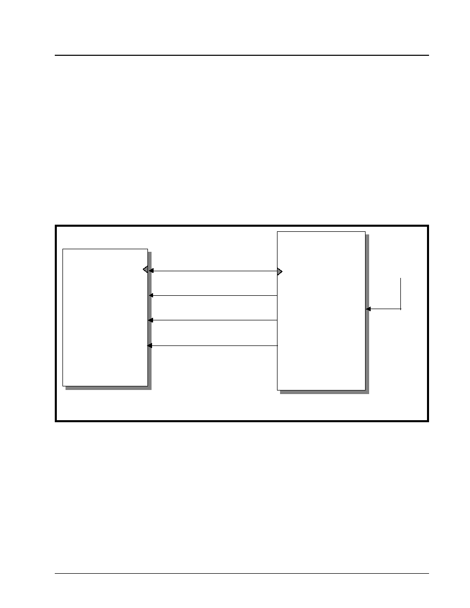
·Á
·Á
·Á
·Á
XRT7250
DS3/E3 FRAMER IC
REV. 1.1.1
425
Operation of the Receive Payload Data Output In-
terface block
The Receive Payload Data Output Interface permits
the user to read out the payload data of Inbound E3
frames, via either of the following modes.
∑ Serial Mode
∑ Nibble-Parallel Mode
Each of these modes are described in detail, below.
6.3.5.1
Serial Mode Operation Behavior of the
XRT7250
If the XRT7250 has been configured to operate in this
mode, then the XRT7250 will behave as follows.
Payload Data Output
The XRT7250 will output the payload data, of the in-
coming E3 frames, upon the rising edge of RxClk.
Delineation of Inbound DS3 Frames
The XRT7250 will pulse the RxFrame output pin
"High" for one bit-period, coincident with it driving the
first bit within a given E3 frame, via the RxSer output
pin.
Interfacing the XRT7250 to the Receive Terminal
Equipment
Figure 209 presents a simple illustration as how the
user should interface the XRT7250 to that terminal
equipment which processes Receive Direction pay-
load data.
Required Operation of the Terminal Equipment
The XRT7250 will update the data on the RxSer out-
put pin, upon the rising edge of RxClk. Hence, the
Terminal Equipment should sample the data on the
RxSer output pin (or the E3_Data_In pin at the Termi-
nal Equipment) upon the rising edge of RxClk. As the
Terminal Equipment samples RxSer with each rising
edge of RxClk it should also be sampling the follow-
ing signals.
∑ RxFrame
∑ RxOHInd
The Need for sampling RxFrame
The XRT7250 will pulse the RxFrame output pin
"High" coincident with it driving the very first bit of a
given E3 frame onto the RxSer output pin. If knowl-
edge of the E3 Frame Boundaries is important for the
operation of the Terminal Equipment, then this is a
very important signal for it to sample.
The Need for sampling RxOHInd
The XRT7250 will indicate that it is currently driving
an overhead bit onto the RxSer output pin, by pulsing
the RxOHInd output pin "High". If the Terminal Equip-
ment samples this signal "High", then it should know
that the bit, that it is currently sampling via the RxSer
pin is an overhead bit and should not be processed.
F
IGURE
209. I
LLUSTRATION
OF
THE
R
ECEIVE
P
AYLOAD
D
ATA
O
UTPUT
I
NTERFACE
B
LOCK
(
OF
THE
XRT7250 DS3/
E3 F
RAMER
IC)
BEING
INTERFACED
TO
THE
R
ECEIVE
T
ERMINAL
E
QUIPMENT
(S
ERIAL
M
ODE
O
PERATION
)
Terminal Equipment
(Receive Payload Section)
XRT7250 E3 Framer
E3_Data_In
Rx_E3_Clock_In
Rx_Start_of_Frame
RxClk
RxFrame
RxOHInd
34.368 MHz Clock Signal
RxSer
Rx_E3_OH_Ind
RxLineClk
34.368 MHz
Clock Source
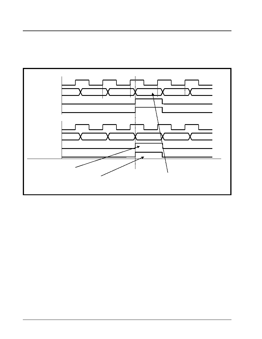
XRT7250
·Á
·Á
·Á
·Á
DS3/E3 FRAMER IC
REV. 1.1.1
426
The Behavior of the Signals between the Receive
Payload Data Output Interface block and the Ter-
minal Equipment
The behavior of the signals between the XRT7250
and the Terminal Equipment for E3 Serial Mode Op-
eration is illustrated in Figure 210.
6.3.5.2
Nibble-Parallel Mode OperationBehav-
ior of the XRT7250
If the XRT7250 has been configured to operate in the
Nibble-Parallel Mode, then the XRT7250 will behave
as follows.
Payload Data Output
The XRT7250 will output the payload data of the in-
coming E3 frames, via the RxNib[3:0] output pins, up-
on the rising edge of RxClk.
N
OTES
:
1. In this case, RxClk will function as the Nibble Clock
signal between the XRT7250 the Terminal Equip-
ment. The XRT7250 will pulse the RxClk output
signal "High" 1060 times, for each Inbound E3
frame.
2. Unlike Serial Mode operation, the duty cycle of
RxClk, in Nibble-Parallel Mode operation is approx-
imately 25%.
Delineation of Inbound DS3 Frames
The XRT7250 will pulse the RxFrame output pin
"High" for one nibble-period coincident with it driving
the very first nibble, within a given Inbound E3 frame,
via the RxNib[3:0] output pins.
Interfacing the XRT7250 the Terminal Equipment.
Figure 211 presents a simple illustration as how the
user should interface the XRT7250 to that terminal
equipment which processes Receive Direction pay-
load data.
F
IGURE
210. A
N
I
LLUSTRATION
OF
THE
BEHAVIOR
OF
THE
SIGNALS
BETWEEN
THE
R
ECEIVE
P
AYLOAD
D
ATA
O
UT
-
PUT
I
NTERFACE
BLOCK
OF
THE
XRT7250
AND
THE
T
ERMINAL
E
QUIPMENT
Terminal Equipment Signals
E3_Clock_In
E3_Data_In
Rx_Start_of_Frame
E3_Overhead_Ind
XRT7250 Receive Payload Data I/F Signals
RxClk
RxSer
RxFrame
RxOH_Ind
Payload[4238]
Payload4239]
FA1, Bit 7
FA1, Bit 6
Payload[4238]
Payload[4239]
FA1, Bit 7
FA1, Bit 6
Note: FA1 and FA2 bytes will not be processed by the
Transmit Payload Data Input Interface.
E3 Frame Number N
E3 Frame Number N + 1
Note: RxFrame pulses high to denote
E3 Frame Boundary.
Note: RxOH_Ind pulses high to
denote Overhead Data
(e.g., the FA1 and FA2 Bytes).
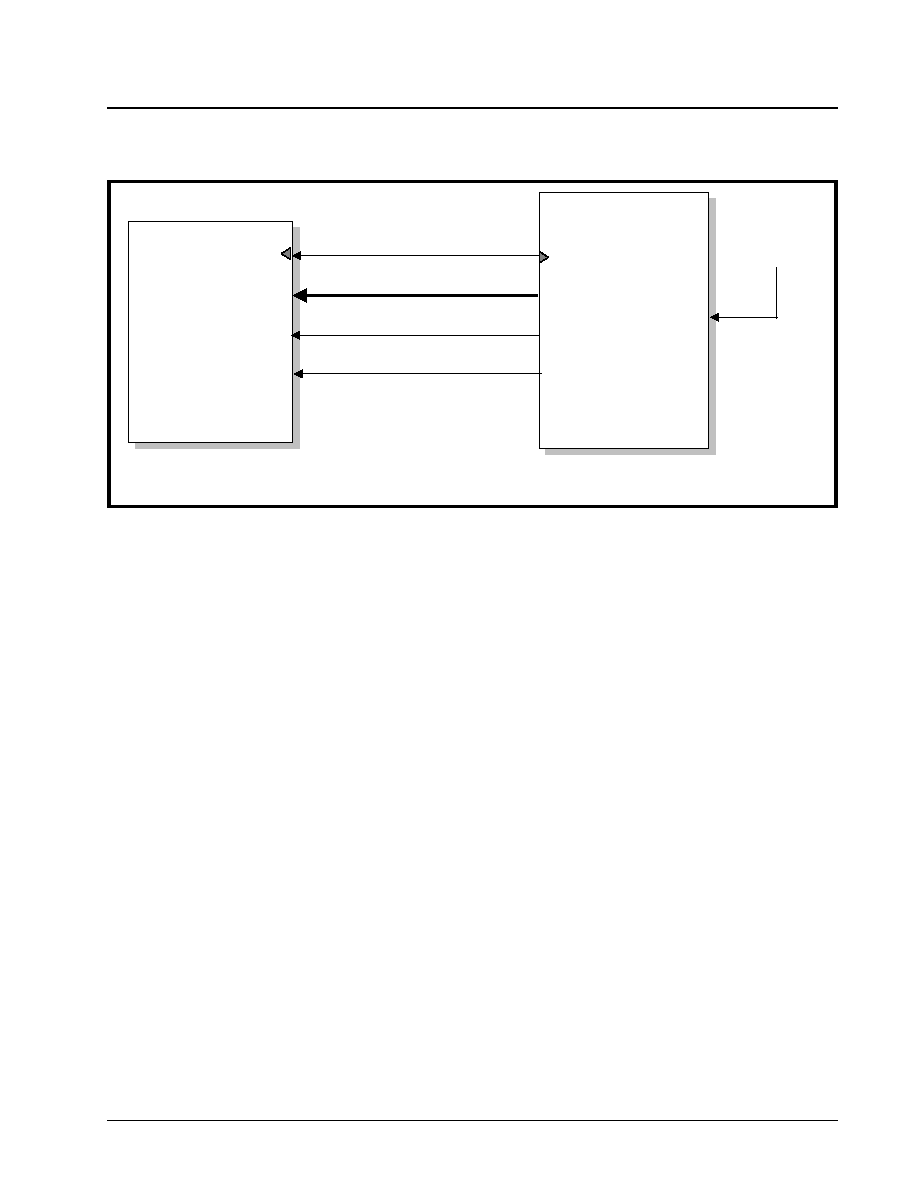
·Á
·Á
·Á
·Á
XRT7250
DS3/E3 FRAMER IC
REV. 1.1.1
427
Required Operation of the Terminal Equipment
The XRT7250 will update the data on the RxNib[3:0]
line, upon the rising edge of RxClk. Hence, the Ter-
minal Equipment should sample the data on the Rx-
Nib[3:0] output pins (or the E3_Data_In[3:0] input
pins at the Terminal Equipment) upon the rising edge
of RxClk. As the Terminal Equipment samples RxSer
with each rising edge of RxClk it should also be sam-
pling the RxFrame signal.
The Need for Sampling RxFrame
The XRT7250 will pulse the RxFrame output pin
"High" coincident with it driving the very first nibble of
a given E3 frame, onto the RxNib[3:0] output pins. If
knowledge of the E3 Frame Boundaries is important
for the operation of the Terminal Equipment, then this
is a very important signal for it to sample.
The Behavior of the Signals between the Receive
Payload Data Output Interface block and the Ter-
minal Equipment
The behavior of the signals between the XRT7250
and the Terminal Equipment for E3 Nibble-Mode op-
eration is illustrated in Figure 212.
F
IGURE
211. I
LLUSTRATION
OF
THE
XRT7250 DS3/E3 F
RAMER
IC
BEING
INTERFACED
TO
THE
R
ECEIVE
S
ECTION
OF
THE
T
ERMINAL
E
QUIPMENT
(N
IBBLE
-M
ODE
O
PERATION
)
Terminal Equipment
(Receive Payload Section)
XRT7250 E3 Framer
E3_Data_In[3:0]
Rx_E3_Clock_In
Rx_Start_of_Frame
RxClk
RxFrame
8.592 MHz Clock Signal
RxNib[3:0]
RxLineClk
34.368 MHz
Clock Source
RxOH_Ind
Rx_E3_OH_Ind
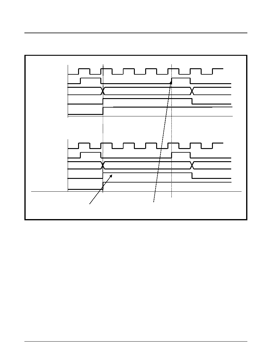
XRT7250
·Á
·Á
·Á
·Á
DS3/E3 FRAMER IC
REV. 1.1.1
428
6.3.6
Receive Section Interrupt Processing
The Receive Section of the XRT7250 can generate
an interrupt to the MIcrocontroller/Microprocessor for
the following reasons.
∑ Change in Receive LOS Condition
∑ Change in Receive OOF Condition
∑ Change in Receive LOF Condition
∑ Change in Receive AIS Condition
∑ Change in Receive FERF Condition
∑ Change of Framing Alignment
∑ Change in Receive Trail Trace Buffer Message
∑ Detection of FEBE (Far-End Block Error) Event
∑ Detection of BIP-8 Error
∑ Detection of Framing Byte Error
∑ Detection of Payload Type Mismatch
∑ Reception of a new LAPD Message
6.3.6.1
Enabling Receive Section Interrupts
As mentioned in Section 1.6, the Interrupt Structure
within the XRT7250 contains two hierarchical levels.
∑ Block Level
∑ Source Level
The Block Level
The Enable state of the Block level for the Receive
Section Interrupts dictates whether or not interrupts
(if enabled at the source level), are actually enabled.
The user can enable or disable these Receive Sec-
tion interrupts, at the Block Level by writing the appro-
priate data into Bit 7 (Rx DS3/E3 Interrupt Enable)
within the Block Interrupt Enable register (Address =
0x04), as illustrated below.
F
IGURE
212. I
LLUSTRATION
OF
THE
SIGNALS
THAT
ARE
OUTPUT
VIA
THE
R
ECEIVE
O
VERHEAD
D
ATA
O
UTPUT
I
NTER
-
FACE
BLOCK
(
FOR
M
ETHOD
2).
XRT7250 Receive Payload Data I/F Signals
E3 Frame Number N
E3 Frame Number N + 1
Note: RxFrame pulses high to denote
E3 Frame Boundary.
Terminal Equipment Signals
RxOutClk
Rx_Start_of_Frame
Rx_E3_Clock_In
E3_Data_In[3:0]
Overhead Nibble [0]
Overhead Nibble [1]
RxOutClk
RxFrame
RxClk
RxNib[3:0]
Overhead Nibble [0]
Overhead Nibble [1]
Recommended Sampling Edge of Terminal
Equipment
Rx_E3_OH_Ind
RxOH_Ind
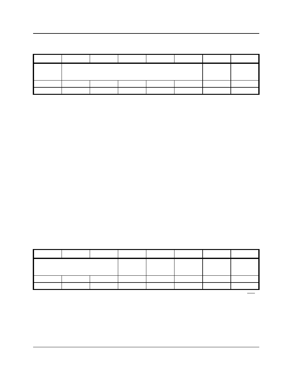
·Á
·Á
·Á
·Á
XRT7250
DS3/E3 FRAMER IC
REV. 1.1.1
429
Setting this bit-field to "1" enables the Receive Sec-
tion at the Block Level) for interrupt generation. Con-
versely, setting this bit-field to "0" disables the Re-
ceive Section for interrupt generation.
6.3.6.2
Enabling/Disabling and Servicing Inter-
rupts
As mentioned earlier, the Receive Section of the
XRT7250 Framer IC contains numerous interrupts.
The Enabling/Disabling and Servicing of each of
these interrupts is described below.
6.3.6.2.1
The Change in Receive LOS Condi-
tion Interrupt
If the Change in Receive LOS Condition Interrupt is
enabled, then the XRT7250 Framer IC will generate
an interrupt in response to either of the following con-
ditions.
1. When the XRT7250 Framer IC declares an LOS
(Loss of Signal) Condition, and
2. When the XRT7250 Framer IC clears the LOS
condition.
Conditions causing the XRT7250 Framer IC to de-
clare an LOS Condition.
∑ If the XRT7300 LIU IC declares an LOS condition,
and drives the RLOS input pin (of the XRT7250
Framer IC) "High".
∑ If the XRT7250 Framer IC detects 32 consecutive
"0", via the RxPOS and RxNEG input pins.
Conditions causing the XRT7250 Framer IC to
clear the LOS Condition.
∑ If the XRT7300 LIU IC clears the LOS condition and
drives the RLOS input pin (of the XRT7250 Framer
IC) "Low".
∑ If the XRT7250 Framer IC detects a string of 32
consecutive bits (via the RxPOS and RxNEG input
pins) that does NOT contain a string of 4 consecu-
tive "0's".
Enabling and Disabling the Change in Receive
LOS Condition Interrupt
The user can enable or disable the Change in Re-
ceive LOS Condition Interrupt, by writing the appror-
priate value into Bit 1 (LOS Interrupt Enable), within
the RxE3 Interrupt Enable Register - 1, as indicated
below.
Setting this bit-field to "1" enables this interrupt. Con-
versely, setting this bit-field to "0" disables this inter-
rupt.
Servicing the Change in Receive LOS Condition
Interrupt
Whenever the XRT7250 Framer IC detects this inter-
rupt, it will do all of the following.
∑ It will assert the Interrupt Request output pin (INT),
by driving it "Low".
∑ It will set Bit 1 (LOS Interrupt Status), within the Rx
E3 Interrupt Status Register - 1 to "1", as indicated
below.
BLOCK INTERRUPT ENABLE REGISTER (ADDRESS = 0X04)
B
IT
7
B
IT
6
B
IT
5
B
IT
4
B
IT
3
B
IT
2
B
IT
1
B
IT
0
RxDS3/E3
Interrupt
Enable
Not Used
TxDS3/E3
Interrupt
Enable
One-Second
Interrupt
Enable
R/W
RO
RO
RO
RO
RO
R/W
R/W
X
0
0
0
0
0
0
0
RXE3 INTERRUPT ENABLE REGISTER - 1 (ADDRESS = 0X12)
B
IT
7
B
IT
6
B
IT
5
B
IT
4
B
IT
3
B
IT
2
B
IT
1
B
IT
0
Not Used
COFA
Interrupt
Enable
OOF
Interrupt
Enable
LOF
Interrupt
Enable
LOS
Interrupt
Enable
AIS
Interrupt
Enable
RO
RO
RO
R/W
R/W
R/W
R/W
R/W
0
0
0
0
0
0
X
0
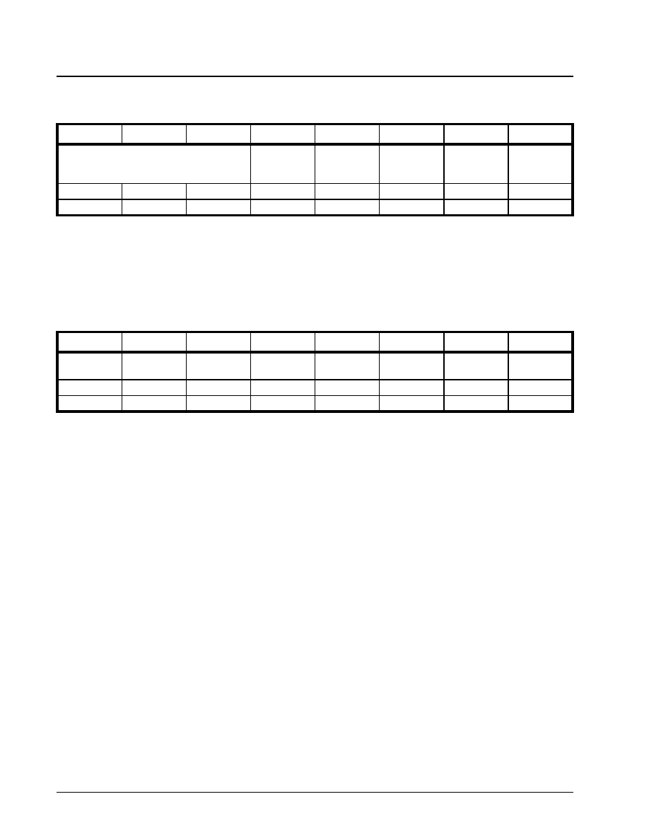
XRT7250
·Á
·Á
·Á
·Á
DS3/E3 FRAMER IC
REV. 1.1.1
430
Whenever the user's system encounters the Change
in Receive LOS Condition Interrupt, then it should do
the following.
1. It should determine the current state of the LOS
condition. Recall, that this interrupt can be gen-
erated, whenever the XRT7250 Framer IC
declares or clears the LOS defect. Hence, the
user can determine the current state of the LOS
defect by reading the state of Bit 4 (RxLOS)
within the Rx E3 Configuration and Status Regis-
ter - 2, as illustrated below.
If the LOS state is TRUE
1. It should transmit a FERF (Far-End-Receive Fail-
ure) indicator to the Remote Terminal Equipment.
The XRT7250 Framer IC automatically supports
this action via the FERF-upon-LOS feature.
If the LOS state is FALSE
1. It should cease transmitting the FERF indication
to the Remote Terminal Equipment. The
XRT7250 Framer IC automatically supports this
action via the FERF-upon-LOS feature.
6.3.6.2.2
The Change in Receive OOF Condi-
tion Interrupt
If the Change in Receive OOF Condition Interrupt is
enabled, then the XRT7250 Framer IC will generate
an interrupt in response to either of the following con-
ditions.
1. When the XRT7250 Framer IC declares an OOF
(Out of Frame) Condition, and
2. When the XRT7250 Framer IC clears the OOF
condition.
Conditions causing the XRT7250 Framer IC to de-
clare an OOF Condition.
∑ If the Receive E3 Framer block (within the XRT7250
Framer IC) detects Framing Byte errors, within four
consecutive incoming E3 frames.
Conditions causing the XRT7250 Framer IC to
clear the OOF Condition.
∑ If the Receive E3 Framer block (within the XRT7250
Framer IC) transitions from the FA1, FA2 Octet Ver-
ification state to the In-Frame state (see Figure
175).
∑ If the Receive E3 Framer block transitions from the
OOF Condition state to the In-Frame state (see Fig-
ure 175).
Enabling and Disabling the Change in Receive
OOF Condition Interrupt
The user can enable or disable the Change in Re-
ceive OOF Condition Interrupt, by writing the appro-
priate value into Bit 3 (OOF Interrupt Enable), within
RXE3 INTERRUPT STATUS REGISTER - 1 (ADDRESS = 0X14)
B
IT
7
B
IT
6
B
IT
5
B
IT
4
B
IT
3
B
IT
2
B
IT
1
B
IT
0
Not Used
COFA
Interrupt
Status
OOF
Interrupt
Status
LOF
Interrupt
Status
LOS
Interrupt
Status
AIS
Interrupt
Status
RO
RO
RO
RUR
RUR
RUR
RUR
RUR
0
0
0
0
0
0
1
0
RXE3 CONFIGURATION & STATUS REGISTER 2 (ADDRESS = 0X11)
B
IT
7
B
IT
6
B
IT
5
B
IT
4
B
IT
3
B
IT
2
B
IT
1
B
IT
0
Rx LOF Algo
RxLOF
RxOOF
RxLOS
RxAIS
RxPld Unstab
Rx
TMark
RxFERF
R/W
RO
RO
RO
RO
RO
RO
RO
X
X
X
X
X
X
X
X
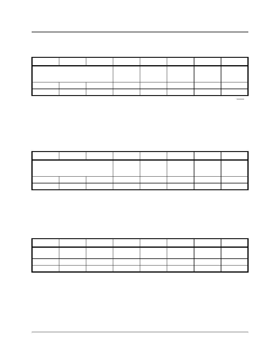
·Á
·Á
·Á
·Á
XRT7250
DS3/E3 FRAMER IC
REV. 1.1.1
431
the RxE3 Interrupt Enable Register - 1, as indicated
below.
Setting this bit-field to "1" enables this interrupt. Con-
versely, setting this bit-field to "0" disables this inter-
rupt.
Servicing the Change in Receive OOF Condition
Interrupt
Whenever the XRT7250 Framer IC detects this inter-
rupt, it will do all of the following.
∑ It will assert the Interrupt Request output pin (INT),
by driving it "Low".
∑ It will set Bit 3 (OOF Interrupt Status), within the Rx
E3 Interrupt Status Register - 1 to "1", as indicated
below.
Whenever the user's system encounters the Change
in Receive OOF Condition Interrupt, then it should do
the following.
1. It should determine the current state of the OOF
condition. Recall, that this interrupt can be gen-
erated, whenever the XRT7250 Framer IC
declares or clears the OOF defect. Hence, the
user can determine the current state of the LOS
defect by reading the state of Bit 5 (RxOOF)
within the Rx E3 Configuration and Status Regis-
ter - 2, as illustrated below.
If the OOF state is TRUE
1. It should transmit a FERF (Far-End-Receive Fail-
ure) indicator to the Remote Terminal Equipment.
The XRT7250 Framer IC automatically supports
this action via the FERF-upon-OOF feature.
If the OOF state is FALSE
1. It should cease transmitting the FERF indication
to the Remote Terminal Equipment. The
XRT7250 Framer IC automatically supports this
action via the FERF-upon-OOF feature.
6.3.6.2.3
The Change in Receive LOF Condi-
tion Interrupt
If the Change in Receive LOF Condition Interrupt is
enabled, then the XRT7250 Framer IC will generate
an interrupt in response to either of the following con-
ditions.
RXE3 INTERRUPT ENABLE REGISTER - 1 (ADDRESS = 0X12)
B
IT
7
B
IT
6
B
IT
5
B
IT
4
B
IT
3
B
IT
2
B
IT
1
B
IT
0
Not Used
COFA
Interrupt
Enable
OOF
Interrupt
Enable
LOF
Interrupt
Enable
LOS
Interrupt
Enable
AIS
Interrupt
Enable
RO
RO
RO
R/W
R/W
R/W
R/W
R/W
0
0
0
0
0
0
X
0
RXE3 INTERRUPT STATUS REGISTER - 1 (ADDRESS = 0X14)
B
IT
7
B
IT
6
B
IT
5
B
IT
4
B
IT
3
B
IT
2
B
IT
1
B
IT
0
Not Used
COFA
Interrupt
Status
OOF
Interrupt
Status
LOF
Interrupt
Status
LOS
Interrupt
Status
AIS
Interrupt
Status
RO
RO
RO
RUR
RUR
RUR
RUR
RUR
0
0
0
0
0
0
1
0
RXE3 CONFIGURATION & STATUS REGISTER 2 (ADDRESS = 0X11)
B
IT
7
B
IT
6
B
IT
5
B
IT
4
B
IT
3
B
IT
2
B
IT
1
B
IT
0
Rx LOF Algo
RxLOF
RxOOF
RxLOS
RxAIS
RxPld Unstab
Rx
TMark
RxFERF
R/W
RO
RO
RO
RO
RO
RO
RO
X
X
X
X
X
X
X
X
XRT7250
·Á
·Á
·Á
·Á
DS3/E3 FRAMER IC
REV. 1.1.1
432
1. When the XRT7250 Framer IC declares an LOF
(Out of Frame) Condition, and
2. When the XRT7250 Framer IC clears the LOF
condition.
Conditions causing the XRT7250 Framer IC to de-
clare an LOF Condition.
∑ If the Receive E3 Framer block (within the XRT7250
Framer IC) detects Framing Byte errors, within four
consecutive incoming E3 frames and is not able to
transition back into the In-Frame state within 1 or
3ms.
Conditions causing the XRT7250 Framer IC to
clear the LOF Condition.
∑ If the Receive E3 Framer block transitions from the
OOF Condition state to the LOF Condition state
(see Figure 175).
∑ If the Receive E3 Framer block transitions back into
the In-Frame state.
Enabling and Disabling the Change in Receive
LOF Condition Interrupt
The user can enable or disable the Change in Re-
ceive LOF Condition Interrupt, by writing the appropri-
ate value into Bit 3 (LOF Interrupt Enable), within the
RxE3 Interrupt Enable Register - 1, as indicated be-
low.
Setting this bit-field to "1" enables this interrupt. Con-
versely, setting this bit-field to "0" disables this inter-
rupt.
Servicing the Change in Receive LOF Condition
Interrupt
Whenever the XRT7250 Framer IC detects this inter-
rupt, it will do all of the following.
∑ It will assert the Interrupt Request output pin (INT),
by driving it "Low".
∑ It will set Bit 6 (LOF Interrupt Status), within the Rx
E3 Interrupt Status Register - 1 to "1", as indicated
below.
6.3.6.2.4
The Change of Framing Alignment
(COFA) Interrupt
If the Change of Framing Alignment Interrupt is en-
abled then the XRT7250 Framer IC will generate an
interrupt any time the Receive E3 Framer block de-
tects an abrupt change of framing alignment.
N
OTE
: This interrupt is typically accompanied with the
Change in Receive OOF Condition interrupt as well.
Conditions causing the XRT7250 Framer IC to
generate this interrupt.
If the XRT7250 Framer detects receives at least four
consecutive E3 frames, within its Framing Alignment
bytes in Error, then the XRT7250 Framer IC will de-
clare an OOF condition. However, while the
XRT7250 Framer IC is operating in the OOF condi-
tion, it will still rely on the old framing alignment for E3
payload data extraction, etc.
However, if the Receive E3 Framer had to change
alignment, in order to re-acquire frame synchroniza-
tion, then this interrupt will occur.
Enabling and Disabling the Change of Framing
Alignment Interrupt
The user can enable or disable the Change of Fram-
ing Alignment Interrupt by writing the appropriate val-
ue into Bit 4 (COFA Interrupt
RXE3 INTERRUPT ENABLE REGISTER - 1 (ADDRESS = 0X12)
B
IT
7
B
IT
6
B
IT
5
B
IT
4
B
IT
3
B
IT
2
B
IT
1
B
IT
0
Not Used
COFA
Interrupt
Enable
OOF
Interrupt
Enable
LOF
Interrupt
Enable
LOS
Interrupt
Enable
AIS
Interrupt
Enable
RO
RO
RO
R/W
R/W
R/W
R/W
R/W
0
0
0
0
0
0
X
0
RXE3 CONFIGURATION & STATUS REGISTER 2 (ADDRESS = 0X11)
B
IT
7
B
IT
6
B
IT
5
B
IT
4
B
IT
3
B
IT
2
B
IT
1
B
IT
0
Rx LOF Algo
RxLOF
RxOOF
RxLOS
RxAIS
RxPld Unstab
Rx
TMark
RxFERF
R/W
RO
RO
RO
RO
RO
RO
RO
X
X
X
X
X
X
X
X
·Á
·Á
·Á
·Á
XRT7250
DS3/E3 FRAMER IC
REV. 1.1.1
433
Writing a "1" into this bit-field enables the Change of
Framing Alignment Interrupt. Conversely, writing a
"0" into this bit-field disables the Change of Framing
Alignment Interrupt.
Servicing the Change of Framing Alignment Interrupt
Whenever the XRT7250 Framer IC generates this in-
terrupt, it will do the following.
∑ It will assert the Interrupt Request output pin (INT)
by driving it "Low".
∑ It will set Bit 4 (COFA Interrupt Status), within the
Rx E3 Interrupt Status Register -2, to "1", as indi-
cated below.
6.3.6.2.5
The Change in Receive AIS Condition
Interrupt
If the Change in Receive AIS Condition Interrupt is
enabled, then the XRT7250 Framer IC will generate
an interrupt in response to either of the following con-
ditions.
1. When the XRT7250 Framer IC declares an AIS
(Loss of Signal) Condition, and
2. When the XRT7250 Framer IC clears the AIS
condition.
Conditions causing the XRT7250 Framer IC to de-
clare an AIS Condition.
∑ If the XRT7250 Framer IC detects 7 or less "0"
within 2 consecutive E3 frames.
Conditions causing the XRT7250 Framer IC to
clear the AIS Condition.
∑ If the XRT7250 Framer IC detects 2 consecutive E3
frames that each contain 8 or more "0's".
Enabling and Disabling the Change in Receive
AIS Condition Interrupt
The user can enable or disable the Change in Re-
ceive LOS Condition Interrupt, by writing the appro-
priate value into Bit 0 (AIS Interrupt Enable), within
the RxE3 Interrupt Enable Register - 1, as indicated
below.
Setting this bit-field to "1" enables this interrupt. Con-
versely, setting this bit-field to "0" disables this inter-
rupt.
RXE3 INTERRUPT ENABLE REGISTER - 1 (ADDRESS = 0X12)
B
IT
7
B
IT
6
B
IT
5
B
IT
4
B
IT
3
B
IT
2
B
IT
1
B
IT
0
Not Used
COFA
Interrupt
Enable
OOF
Interrupt
Enable
LOF
Interrupt
Enable
LOS
Interrupt
Enable
AIS
Interrupt
Enable
RO
RO
RO
R/W
R/W
R/W
R/W
R/W
0
0
0
X
0
0
0
0
RXE3 INTERRUPT STATUS REGISTER - 1 (ADDRESS = 0X14)
B
IT
7
B
IT
6
B
IT
5
B
IT
4
B
IT
3
B
IT
2
B
IT
1
B
IT
0
Not Used
COFA
Interrupt
Status
OOF
Interrupt
Status
LOF
Interrupt
Status
LOS
Interrupt
Status
AIS
Interrupt
Status
RO
RO
RO
RUR
RUR
RUR
RUR
RUR
0
0
0
1
0
0
0
0
RXE3 INTERRUPT ENABLE REGISTER - 1 (ADDRESS = 0X12)
B
IT
7
B
IT
6
B
IT
5
B
IT
4
B
IT
3
B
IT
2
B
IT
1
B
IT
0
Not Used
COFA
Interrupt
Enable
OOF
Interrupt
Enable
LOF
Interrupt
Enable
LOS
Interrupt
Enable
AIS
Interrupt
Enable
RO
RO
RO
R/W
R/W
R/W
R/W
R/W
0
0
0
0
0
0
X
0
XRT7250
·Á
·Á
·Á
·Á
DS3/E3 FRAMER IC
REV. 1.1.1
434
Servicing the Change in Receive AIS Condition
Interrupt
Whenever the XRT7250 Framer IC detects this inter-
rupt, it will do all of the following.
∑ It will assert the Interrupt Request output pin (INT),
by driving it "Low".
∑ It will set Bit 0 (AIS Interrupt Status), within the Rx
E3 Interrupt Status Register - 1 to "1", as indicated
below.
Whenever the user's system encounters the Change
in Receive AIS Condition Interrupt, then it should do
the following.
1. It should determine the current state of the AIS
condition. Recall, that this interrupt can be gen-
erated, whenever the XRT7250 Framer IC
declares or clears the AIS defect. Hence, the
user can determine the current state of the AIS
defect by reading the state of Bit 4 (RxAIS) within
the Rx E3 Configuration and Status Register - 2,
as illustrated below.
If the AIS Condition is TRUE
1. It should begin transmitting the FERF indication
to the Remote Terminal Equipment. The
XRT7250 Framer IC automatically supports this
action via the FERF-upon-AIS feature.
If the AIS Condition is FALSE
2. It should cease transmitting the FERF indication
to the Remote Terminal Equipment. The
XRT7250 Framer IC automatically supports this
action via the FERF-upon-AIS feature.
6.3.6.2.6
The Change in Trail Trace Buffer Mes-
sage Interrupt
If the Change in Trail Trace Buffer Message Interrupt
has been enabled, then the XRT7250 Framer IC will
generate an interrupt any time the Receive E3 Framer
block receives a different Trail Trace Buffer message,
then it has previously read in.
Enabling and Disabling the Change in Trail Trace
Buffer Message Interrupt.
The user can enable or disable the Change in Trail
Trace Buffer Message interrupt by writing the appro-
priate value into Bit 6 (TTB Change Interrupt Enable)
within the Rx E3 Interrupt Enable Register - 2, as indi-
cated below.
RXE3 INTERRUPT STATUS REGISTER - 1 (ADDRESS = 0X14)
B
IT
7
B
IT
6
B
IT
5
B
IT
4
B
IT
3
B
IT
2
B
IT
1
B
IT
0
Not Used
COFA
Interrupt
Status
OOF
Interrupt
Status
LOF
Interrupt
Status
LOS
Interrupt
Status
AIS
Interrupt
Status
RO
RO
RO
RUR
RUR
RUR
RUR
RUR
0
0
0
0
0
0
1
0
RXE3 CONFIGURATION & STATUS REGISTER 2 (ADDRESS = 0X11)
B
IT
7
B
IT
6
B
IT
5
B
IT
4
B
IT
3
B
IT
2
B
IT
1
B
IT
0
Rx LOF Algo
RxLOF
RxOOF
RxLOS
RxAIS
RxPld Unstab
Rx
TMark
RxFERF
R/W
RO
RO
RO
RO
RO
RO
RO
X
X
X
X
X
X
X
X
RXE3 INTERRUPT ENABLE REGISTER - 2 (ADDRESS = 0X13)
B
IT
7
B
IT
6
B
IT
5
B
IT
4
B
IT
3
B
IT
2
B
IT
1
B
IT
0
Not Used
TTB
Change
Interrupt
Enable
Not Used
FEBE
Interrupt
Enable
FERF
Interrupt
Enable
BIP-8
Error Interrupt
Enable
Framing
Byte Error
Interrupt
Enable
RxPld
Mis
Interrupt
Enable
RO
R/W
RO
R/W
R/W
R/W
R/W
R/W
0
0
0
0
X
0
0
0

·Á
·Á
·Á
·Á
XRT7250
DS3/E3 FRAMER IC
REV. 1.1.1
435
Writing a "1" into this bit-field enables the Change in
Trail Trace Buffer Message Interrupt. Conversely,
writing a "0" into this bit-field disables the Change in
Trail Trace Buffer Message Interrupt.
Servicing the Change in Trail Trace Buffer Mes-
sage Interrupt
Whenever the XRT7250 Framer IC generates this in-
terrupt, it will do the following.
∑ It will assert the Interrupt Request output pin (INT)
by driving it "Low".
∑ It will set Bit 6 (TTB Change Interrupt Status),
within the Rx E3 Interrupt Status Register - 2, as
indicated below.
∑ It will write the contents of this newly received Trail
Trace Buffer Message, into the RxTTB-0 (located at
0x1C) through RxTTB-15 (located at 0x2B) regis-
ters.
Whenever the Terminal Equipment encounters the
Change in Trail Trace Buffer Message Interrupt, then
it should read out the contents of the 16 RxTTB regis-
ters.
6.3.6.2.7
The Change in Receive FERF Condi-
tion Interrupt
If the Change in Receive FERF Condition Interrupt is
enabled, then the XRT7250 Framer IC will generate
an interrupt in response to either of the following con-
ditions.
1. When the XRT7250 Framer IC declares a FERF
(Far-End Receive Failure) Condition, and
2. When the XRT7250 Framer IC clears the FERF
condition.
Conditions causing the XRT7250 Framer IC to de-
clare an FERF Condition.
∑ If the XRT7250 Framer IC begins receiving E3
frames which have the FERF bit (within the MA
byte, set to "1").
Conditions causing the XRT7250 Framer IC to
clear the AIS Condition.
∑ If the XRT7250 Framer IC begins receiving E3
frames that do NOT have the FERF bit set to "1".
Enabling and Disabling the Change in Receive
AIS Condition Interrupt
The user can enable or disable the Change in Re-
ceive FERF Condition Interrupt, by writing the appro-
priate value into Bit 3 (FERF Interrupt Enable), within
the RxE3 Interrupt Enable Register - 2, as indicated
below.
Setting this bit-field to "1" enables this interrupt. Con-
versely, setting this bit-field to "0" disables this inter-
rupt.
Servicing the Change in Receive FERF Condition
Interrupt
Whenever the XRT7250 Framer IC detects this inter-
rupt, it will do all of the following.
∑ It will assert the Interrupt Request output pin (INT),
by driving it "Low".It will set Bit 3 (FERF Interrupt
RXE3 INTERRUPT STATUS REGISTER - 2 (ADDRESS = 0X15)
B
IT
7
B
IT
6
B
IT
5
B
IT
4
B
IT
3
B
IT
2
B
IT
1
B
IT
0
Not Used
TTB
Change
Interrupt
Status
Not Used
FEBE
Interrupt
Status
FERF
Interrupt
Status
BIP-8
Error Interrupt
Status
Framing
Byte Error
Interrupt
Status
RxPld
Mis
Interrupt
Status
RO
RUR
RO
RUR
RUR
RUR
RUR
RUR
0
1
0
0
0
0
0
0
RXE3 INTERRUPT ENABLE REGISTER - 2 (ADDRESS = 0X13)
B
IT
7
B
IT
6
B
IT
5
B
IT
4
B
IT
3
B
IT
2
B
IT
1
B
IT
0
Not Used
TTB
Change
Interrupt
Enable
Not Used
FEBE
Interrupt
Enable
FERF
Interrupt
Enable
BIP-8
Error Interrupt
Enable
Framing
Byte Error
Interrupt
Enable
RxPld
Mis
Interrupt
Enable
RO
R/W
RO
R/W
R/W
R/W
R/W
R/W
0
0
0
0
X
0
0
0
XRT7250
·Á
·Á
·Á
·Á
DS3/E3 FRAMER IC
REV. 1.1.1
436
Status), within the Rx E3 Interrupt Status Register -
2 to "1", as indicated below
Whenever the user's system encounters the Change
in Receive FERF Condition Interrupt, then it should
do the following.
1. It should determine the current state of the FERF
condition. Recall, that this interrupt can be gen-
erated, whenever the XRT7250 Framer IC
declares or clears the FERF defect. Hence, the
user can determine the current state of the LOS
defect by reading the state of Bit 0 (RxFERF)
within the Rx E3 Configuration and Status Regis-
ter - 2, as illustrated below.
6.3.6.2.8
The Detection of FEBE (Far-End-
Block Error) Event Interrupt
If the Detection of FEBE Event Interrupt is enabled,
then the XRT7250 Framer IC will generate an inter-
rupt, anytime the Receive E3 Framer block has re-
ceived an E3 frame with the FEBE bit-field (within the
MA byte) set to "1".
Enabling and Disabling the Detection of FEBE
Event Interrupt
The user can enable or disable the Detection of
FEBE Event' interrupt by writing the appropriate value
into Bit 4 (FEBE Interrupt Enable) within the Rx E3 In-
terrupt Enable Register - 2, as indicated below.
Setting this bit-field to "1" enables this interrupt. Con-
versely, setting this bit-field to "0" disables this inter-
rupt.
Servicing the Detection of the FEBE Event Inter-
rupt
Whenever the XRT7250 Framer IC detects this inter-
rupt, it will do the following.
∑ It will assert the Interrupt Request output pin (INT),
by driving it "High".It will set the Bit 4 (FEBE Inter-
rupt Status), within the RxE3 Interrupt Status Reg-
ister - 2 as indicated below.
RXE3 INTERRUPT STATUS REGISTER - 2 (ADDRESS = 0X15)
B
IT
7
B
IT
6
B
IT
5
B
IT
4
B
IT
3
B
IT
2
B
IT
1
B
IT
0
Not Used
TTB
Change
Interrupt
Status
Not Used
FEBE
Interrupt
Status
FERF
Interrupt
Status
BIP-8
Error Interrupt
Status
Framing
Byte Error
Interrupt
Status
RxPld
Mis
Interrupt
Status
RO
RUR
RO
RUR
RUR
RUR
RUR
RUR
0
0
0
0
1
0
0
0
RXE3 CONFIGURATION & STATUS REGISTER 2 (ADDRESS = 0X11)
B
IT
7
B
IT
6
B
IT
5
B
IT
4
B
IT
3
B
IT
2
B
IT
1
B
IT
0
Rx LOF Algo
RxLOF
RxOOF
RxLOS
RxAIS
RxPld Unstab
Rx
TMark
RxFERF
R/W
RO
RO
RO
RO
RO
RO
RO
X
X
X
X
X
X
X
X
RXE3 INTERRUPT ENABLE REGISTER - 2 (ADDRESS = 0X13)
B
IT
7
B
IT
6
B
IT
5
B
IT
4
B
IT
3
B
IT
2
B
IT
1
B
IT
0
Not Used
TTB
Change
Interrupt
Enable
Not Used
FEBE
Interrupt
Enable
FERF
Interrupt
Enable
BIP-8
Error Interrupt
Enable
Framing
Byte Error
Interrupt
Enable
RxPld
Mis
Interrupt
Enable
RO
R/W
RO
R/W
R/W
R/W
R/W
R/W
0
0
0
X
X
0
0
0

·Á
·Á
·Á
·Á
XRT7250
DS3/E3 FRAMER IC
REV. 1.1.1
437
Whenever the Terminal Equipment encounters the
Detection of FEBE Event Interrupt, it should do the
following.
∑ It should read the contents of the PMON FEBE
Event Count Registers (located at Addresses 0x56
and 0x57) in order to determine the number of
FEBE Events that have been received by the
XRT7250 Framer IC.
6.3.6.2.9
The Detection of BIP-8 Error Interrupt
If the Detection of BIP-8 Error Interrupt is enabled,
then the XRT7250 Framer IC will generate an inter-
rupt, anytime the Receive E3 Framer block has de-
tected an error in the EM (Error Monitoring) byte,
within an incoming E3 frame.
Enabling and Disabling the Detection of FEBE
Event Interrupt
The user can enable or disable the Detection of BIP-8
Error' interrupt by writing the appropriate value into
Bit 2 (BIP-8 Interrupt Enable) within the Rx E3 Inter-
rupt Enable Register - 2, as indicated below.
Setting this bit-field to "1" enables this interrupt. Con-
versely, setting this bit-field to "0" disables this inter-
rupt.
Servicing the Detection of the BIP-8 Error Inter-
rupt
Whenever the XRT7250 Framer IC detects this inter-
rupt, it will do the following.
∑ It will assert the Interrupt Request output pin (INT),
by driving it "High".
∑ It will set the Bit 2 (BIP-8 Interrupt Status), within
the RxE3 Interrupt Status Register - 2 as indicated
below.
Whenever the Terminal Equipment encounters the
Detection of BIP-8 Error Interrupt, it should do the fol-
lowing.
RXE3 INTERRUPT STATUS REGISTER - 2 (ADDRESS = 0X15)
B
IT
7
B
IT
6
B
IT
5
B
IT
4
B
IT
3
B
IT
2
B
IT
1
B
IT
0
Not Used
TTB
Change
Interrupt
Status
Not Used
FEBE
Interrupt
Status
FERF
Interrupt
Status
BIP-8
Error Interrupt
Status
Framing
Byte Error
Interrupt
Status
RxPld
Mis
Interrupt
Status
RO
RUR
RO
RUR
RUR
RUR
RUR
RUR
0
0
0
1
0
0
0
0
RXE3 INTERRUPT ENABLE REGISTER - 2 (ADDRESS = 0X13)
B
IT
7
B
IT
6
B
IT
5
B
IT
4
B
IT
3
B
IT
2
B
IT
1
B
IT
0
Not Used
TTB
Change
Interrupt
Enable
Not Used
FEBE
Interrupt
Enable
FERF
Interrupt
Enable
BIP-8
Error
Interrupt
Enable
Framing
Byte Error
Interrupt
Enable
RxPld
Mis
Interrupt
Enable
RO
R/W
RO
R/W
R/W
R/W
R/W
R/W
0
0
0
X
X
0
0
0
RXE3 INTERRUPT STATUS REGISTER - 2 (ADDRESS = 0X15)
B
IT
7
B
IT
6
B
IT
5
B
IT
4
B
IT
3
B
IT
2
B
IT
1
B
IT
0
Not Used
TTB
Change
Interrupt
Status
Not Used
FEBE
Interrupt
Status
FERF
Interrupt
Status
BIP-8
Error
Interrupt
Status
Framing
Byte Error
Interrupt
Status
RxPld
Mis
Interrupt
Status
RO
RUR
RO
RUR
RUR
RUR
RUR
RUR
0
0
0
0
0
1
0
0

XRT7250
·Á
·Á
·Á
·Á
DS3/E3 FRAMER IC
REV. 1.1.1
438
∑ It should read the contents of the PMON Parity
Error Event Count Registers (located at Addresses
0x54 and 0x55) in order to determine the number of
BIP-8 Errors that have been received by the
XRT7250 Framer IC.
6.3.6.2.10 The Detection of Framing Byte Error
Interrupt
If the Detection of Framing Byte Error Interrupt is en-
abled, then the XRT7250 Framer IC will generate an
interrupt, anytime the Receive E3 Framer block has
received an E3 frame with an incorrect Framing Byte
(e.g., FA1 or FA2) value.
Enabling and Disabling the Detection of FEBE
Event Interrupt
The user can enable or disable the Detection of
Framing Byte Error' interrupt by writing the appropri-
ate value into Bit 1 (Framing Byte Error Interrupt En-
able) within the Rx E3 Interrupt Enable Register - 2,
as indicated below.
Setting this bit-field to "1" enables this interrupt. Con-
versely, setting this bit-field to "0" disables this inter-
rupt.
Servicing the Detection of Framing Byte Error In-
terrupt
Whenever the XRT7250 Framer IC detects this inter-
rupt, it will do the following.
∑ It will assert the Interrupt Request output pin (INT),
by driving it "High".
∑ It will set the Bit 4 (Framing Byte Error Interrupt Sta-
tus), within the RxE3 Interrupt Status Register - 2
as indicated below.
Whenever the Terminal Equipment encounters the
Detection of Framing Byte Error Interrupt, it should do
the following.
∑ It should read the contents of the PMON Framing
Bit/Byte Error Count Registers (located at
Addresses 0x52 and 0x53) in order to determine
the number of Framing Byte errors that have been
received by the XRT7250 Framer IC.
6.3.6.2.11 The Detection of Payload Type Mis-
match Interrupt
If the Detection of Payload Type Mismatch Interrupt is
enabled, then the XRT7250 Framer IC will generate
an interrupt, anytime the Receive E3 Framer block re-
ceives a MA byte (within an incoming E3 frame) that
contents a Payload Type value that is different from
the expected Payload Type value.
Conditions causing this interrupt to be generated.
During system configuration, the user is expected to
specify the Payload Type value that is expected of the
Receive E3 Framer to receive (within each E3 frame),
by writing this value into the RxPLDExp[2:0] bit-fields
within the Rx E3 Configuration & Status Register - 1,
as indicated below.
As long as the Receive E3 Framer block receives E3
frames that contains this Payload Type value, no in-
terrupt will be generated. However, the instant that it
receives an E3 frame, that contains a different Pay-
RXE3 INTERRUPT ENABLE REGISTER - 2 (ADDRESS = 0X13)
B
IT
7
B
IT
6
B
IT
5
B
IT
4
B
IT
3
B
IT
2
B
IT
1
B
IT
0
Not Used
TTB
Change
Interrupt
Enable
Not Used
FEBE
Interrupt
Enable
FERF
Interrupt
Enable
BIP-8
Error Interrupt
Enable
Framing
Byte Error
Interrupt
Enable
RxPld
Mis
Interrupt
Enable
RO
R/W
RO
R/W
R/W
R/W
R/W
R/W
0
0
0
X
X
0
0
0
RXE3 INTERRUPT STATUS REGISTER - 2 (ADDRESS = 0X15)
B
IT
7
B
IT
6
B
IT
5
B
IT
4
B
IT
3
B
IT
2
B
IT
1
B
IT
0
Not Used
TTB
Change
Interrupt
Status
Not Used
FEBE
Interrupt
Status
FERF
Interrupt
Status
BIP-8
Error Interrupt
Status
Framing
Byte Error
Interrupt
Status
RxPld
Mis
Interrupt
Status
RO
RUR
RO
RUR
RUR
RUR
RUR
RUR
0
0
0
1
0
0
0
0
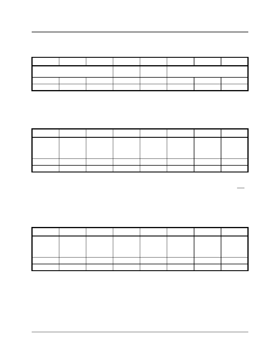
·Á
·Á
·Á
·Á
XRT7250
DS3/E3 FRAMER IC
REV. 1.1.1
439
load Type value, then the XRT7250 Framer IC will
generate this interrupt.
Enabling and Disabling the Detection of Payload
Type Mismatch Interrupt.
The user can enable or disable the Detection of Pay-
load Type Mismatch Interrupt by writing the appropri-
ate data into Bit 0 (RxPld Mis Interrupt Enable), within
the Rx E3 Interrupt Enable Register - 2, as indicated
below.
Setting this bit-field to "1 enables the Detection of
Payload Type Mismatch Interrupt. Conversely, setting
this bit-field to "0" disables the Detection of Payload
Type Mismatch Interrupt.
Servicing the Detection of Payload Type Mis-
match Interrupt
Whenever the XRT7250 Framer IC generates this in-
terrupt, it will do the following.
∑ It will assert the Interrupt Request output pin (INT)
by driving it "Low".
∑ It will set Bit 0 (RxPld Mis Interrupt Status), within
the Rx E3 Interrupt Enable Register -2 to "1", as
indicated below.
6.3.6.2.12 The Receive LAPD Message Interrupt
If the Receive LAPD Message Interrupt is enabled,
then the XRT7250 Framer IC will generate an inter-
rupt anytime the Receive HDLC Controller block has
received a new LAPD Message frame from the Re-
mote Terminal Equipment, and has stored the con-
tents of this message into the Receive LAPD Mes-
sage buffer.
Enabling/Disabling the Receive LAPD Message
Interrupt
The user can enable or disable the Receive LAPD
Message Interrupt by writing the appropriate data into
Bit 1 (RxLAPD Interrupt Enable) within the Rx E3
LAPD Control Register, as indicated below.
RXE3 CONFIGURATION & STATUS REGISTER 1 (ADDRESS = 0X10)
B
IT
7
B
IT
6
B
IT
5
B
IT
4
B
IT
3
B
IT
2
B
IT
1
B
IT
0
RxPLDType[2:0]
RxFERF
Algo
RxTMark
Algo
RxPLDExp[2:0]
RO
RO
RO
RO
RO
R/W
R/W
R/W
0
0
0
0
0
0
0
0
RXE3 INTERRUPT ENABLE REGISTER - 2 (ADDRESS = 0X13)
B
IT
7
B
IT
6
B
IT
5
B
IT
4
B
IT
3
B
IT
2
B
IT
1
B
IT
0
Not Used
TTB
Change
Interrupt
Enable
Not Used
FEBE
Interrupt
Enable
FERF
Interrupt
Enable
BIP-8
Error Interrupt
Enable
Framing
Byte Error
Interrupt
Enable
RxPld
Mis
Interrupt
Enable
RO
R/W
RO
R/W
R/W
R/W
R/W
R/W
0
0
0
X
X
0
0
X
RXE3 INTERRUPT STATUS REGISTER - 2 (ADDRESS = 0X15)
B
IT
7
B
IT
6
B
IT
5
B
IT
4
B
IT
3
B
IT
2
B
IT
1
B
IT
0
Not Used
TTB
Change
Interrupt
Status
Not Used
FEBE
Interrupt
Status
FERF
Interrupt
Status
BIP-8
Error Interrupt
Status
Framing
Byte Error
Interrupt
Status
RxPld
Mis
Interrupt
Status
RO
RUR
RO
RUR
RUR
RUR
RUR
RUR
0
0
0
1
0
0
0
0

XRT7250
·Á
·Á
·Á
·Á
DS3/E3 FRAMER IC
REV. 1.1.1
440
Writing a "1" into this bit-field enables the Receive
LAPD Message Interrupt. Conversely, writing a "0"
into this bit-field disables the Receive LAPD Message
Interrupt.
Servicing the Receive LAPD Message Interrupt
Whenever the XRT7250 Framer IC generates this in-
terrupt, it will do the following.
∑ It will assert the Interrupt Request output pin (INT),
by driving it "Low".
∑ It will set Bit 0 (RxLAPD Interrupt Status), within the
Rx E3 LAPD Control register to "1", as indicated
below.
∑ It will write the contents of the newly Received
LAPD Message into the Receive LAPD Message
buffer (located at 0xDE through 0x135).
Whenever the Terminal Equipment encounters the
Receive LAPD Message Interrupt, then it should read
out the contents of the Receive LAPD Message buff-
er, and respond accordingly.
RXE3 LAPD CONTROL REGISTER (ADDRESS = 0X18)
B
IT
7
B
IT
6
B
IT
5
B
IT
4
B
IT
3
B
IT
2
B
IT
1
B
IT
0
Not Used
DL from NR
RxLAPD
Enable
RxLAPD
Interrupt
Enable
RxLAPD
Interrupt
Status
RO
RO
RO
RO
R/W
R/W
R/W
RUR
0
0
0
0
0
0
0
X
RXE3 LAPD CONTROL REGISTER (ADDRESS = 0X18)
B
IT
7
B
IT
6
B
IT
5
B
IT
4
B
IT
3
B
IT
2
B
IT
1
B
IT
0
Not Used
DL from NR
RxLAPD
Enable
RxLAPD
Interrupt
Enable
RxLAPD
Interrupt
Status
RO
RO
RO
RO
R/W
R/W
R/W
RUR
0
0
0
0
0
0
1
1
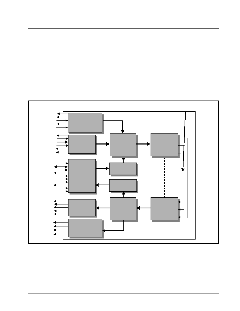
·Á
·Á
·Á
·Á
XRT7250
DS3/E3 FRAMER IC
REV. 1.1.1
441
7.0
DIAGNOSTIC OPERATION OF THE XRT7250
FRAMER IC
The XRT7250 DS3/E3 Framer IC permits the user to
command it to operate in the Framer Local Loop-back
Mode. When the user does this than the data will be
as follows.
1. Data will enter the XRT7250 Framer IC via both
the Transmit Payload Data Input Interface and the
Transmit Overhead Data Input Interface blocks.
2. This data will be processed through the Transmit
DS3/E3 Framer block and the Transmit DS3/E3
LIU Interface block.
3. This Transmit Output data will be internally
looped-back into the Receive Path via the
Receive LIU Interface block.
4. This data will now be processed through the
Receive DS3/E3 Framer block and will ultimately
arrive at both the Receive Payload Data Output
Interface and Receive Overhead Data Output
Interface blocks, where this data will be output to
the terminal equipment.
The Framer Local Loop-back Path is also illustrated
below in Figure 213 .
The user can configure the XRT7250 into the Framer
Local-Loop-back Mode by writing a "1" into bit-field 7
F
IGURE
213. I
LLUSTRATION
OF
THE
F
RAMER
L
OCAL
L
OOP
-
BACK
PATH
,
WITHIN
THE
XRT7250 DS3/E3 F
RAMER
IC
Receive LIU
Interface
Block
Receive DS3/E3
Framer Block
Receive Payload
Data Output
Interface Block
Microprocessor
Interface
MOTO
D[7:0]
A[8:0]
IntB*
CSB*
RdB_DS
WrB_RW
Rdy_Dtck
Reset*
ALE_AS
RxSer
RxNib[3:0]
RxOutClk
RxPOS
RxNEG
RxLineClk
Tx LAPD Buffer/
Controller
Rx LAPD Buffer/
Controller
Receive Overhead
Output
Interface Block
RxNibClk
RxFrame
Transmit
Payload Data
Input
Interface Block
Transmit DS3/E3
Framer Block
Transmit LIU
Interface
Block
TxSer
TxNib[3:0]
TxInClk
TxPOS
TxNEG
TxLineClk
Transmit Overhead
Input
Interface Block
TxOHClk
TxOHIns
TxOHInd
TxOH
TxOHEnable
TxOHFrame
TxNibClk
TxFrame
RxOHFrame
RxOH
RxOHClk
RxOHEnable
Framer Local Loop-back Path

XRT7250
·Á
·Á
·Á
·Á
DS3/E3 FRAMER IC
REV. 1.1.1
442
(Local Loop-back) within the Framer Operating Mode
Register, as illustrated below.
N
OTES
:
1. When the XRT7250 DS3/E3 Framer IC is operating
in the Framer Local-Loop-back Mode, no data will
be output via the TxPOS and TxNEG output pins.
2. The XRT7250 DS3/E3 Framer IC cannot be config-
ured to operate in the Framer Local Loop-back
Mode, if it is configured to operate in Modes 1 or
Mode 4 (Loop-Timing Modes). The user must con-
figure the XRT7250 Framer to operate in one of the
Local-Timing modes.
FRAMER OPERATING MODE REGISTER (ADDRESS = 0X00)
B
IT
7
B
IT
6
B
IT
5
B
IT
4
B
IT
3
B
IT
2
B
IT
1
B
IT
0
Local Loopback
DS3/E3*
Internal
LOS
Enable
RESET
Interrupt
Enable Reset
Frame Format
TimRefSel[1:0]
R/W
R/W
R/W
R/W
R/W
R/W
R/W
R/W
1
X
X
0
X
X
X
X
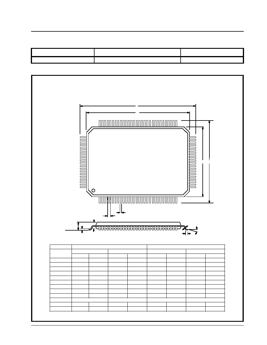
·Á
·Á
·Á
·Á
DS3/E3 FRAMER IC
XRT7250
REV. 1.1.1
443
ORDERING INFORMATION
P
ART
N
UMBER
P
ACKAGE
O
PERATING
T
EMPERATURE
R
ANGE
XRT7250IQ100
100 pin PQFP
-40∞C to +85∞C
PACKAGE DIMENSIONS
80
51
50
31
1
30
81
100
D
D1
E
E1
B
e
A2
A1
A
Seating Plane
L
C
100 LEAD PLASTIC QUAD FLAT PACK
(14 mm x 20 mm, QFP)
Rev. 2.00
1.6 mm Form
1.95 mm Form
INCHES
MILLIMETERS
INCHES
MILLIMETERS
SYMBOL
MIN
MAX
MIN
MAX
MIN
MAX
MIN
MAX
A
0.102
0.130
2.60
3.30
0.102
0.134
2.60
3.40
A
1
0.002
0.010
0.05
0.25
0.002
0.014
0.05
0.35
A
2
0.100
0.120
2.55
3.05
0.100
0.120
2.55
3.05
B
0.009
0.015
0.22
0.38
0.009
0.015
0.22
0.38
C
0.005
0.009
0.13
0.23
0.005
0.009
0.13
0.23
D
0.904
0.923
22.95
23.45
0.931
0.951
23.65
24.15
D
1
0.783
0.791
19.90
20.10
0.783
0.791
19.90
20.10
E
0.667
0.687
16.95
17.45
0.695
0.715
17.65
18.15
E
1
0.547
0.555
13.90
14.10
0.547
0.555
13.90
14.10
e
0.0256 BSC
0.65 BSC
0.0256 BSC
0.65 BSC
L
0.029
0.040
0.73
1.03
0.026
0.037
0.65
0.95
0
∞
7
∞
0
∞
7
∞
0
∞
7
∞
0
∞
7
∞
Note: The control dimension is the millimeter column

·Á
·Á
·Á
·Á
XRT7250
DS3/E3 FRAMER IC
REV. 1.1.1
444
NOTICE
EXAR Corporation reserves the right to make changes to the products contained in this publication in order
to improve design, performance or reliability. EXAR Corporation assumes no responsibility for the use of
any circuits described herein, conveys no license under any patent or other right, and makes no represen-
tation that the circuits are free of patent infringement. Charts and schedules contained here in are only for
illustration purposes and may vary depending upon a user's specific application. While the information in
this publication has been carefully checked; no responsibility, however, is assumed for inaccuracies.
EXAR Corporation does not recommend the use of any of its products in life support applications where
the failure or malfunction of the product can reasonably be expected to cause failure of the life support sys-
tem or to significantly affect its safety or effectiveness. Products are not authorized for use in such applica-
tions unless EXAR Corporation receives, in writing, assurances to its satisfaction that: (a) the risk of injury
or damage has been minimized; (b) the user assumes all such risks; (c) potential liability of EXAR Corpo-
ration is adequately protected under the circumstances.
Copyright 2000 EXAR Corporation
Datasheet March 2001
Reproduction, in part or whole, without the prior written consent of EXAR Corporation is prohibited.
REVISION HISTORY
Rev. P1.0.3 to P1.0.5 Added sections with descriptions of E3 and DS3 operation. Corrected spelling errors
Rev. P1.0.5 to P1.0.6 Minor grammar edits, changed E3 to DS3/E3 in section 1and section 3. Page 45
section 3 changed reference to registers; 0x40 to 0x50, 0x41 to 0x51 and 0x56 to 0x6C. Page 65, RXDS3
Configuration Register table changed bits 0, 1, 2 to R/W.
Rev. P1.0.6 to P1.0.7 Minor corrections, changed some electrical specs.
Rev 1.1.0 removed preliminary designation from data sheet.
Rev. 1.1.1 modified block diagram on page 1.