 | ÐлекÑÑоннÑй компоненÑ: XRT7295AT | СкаÑаÑÑ:  PDF PDF  ZIP ZIP |
Äîêóìåíòàöèÿ è îïèñàíèÿ www.docs.chipfind.ru
XRT7295AT
DS3/Sonet STS-1
Integrated Line Receiver
Rev. 1.20
E
2000
EXAR Corporation, 48720 Kato Road, Fremont, CA 94538 z (510) 668-7000 z FAX (510) 668-7017
December 2000-2
FEATURES
D
Fully Integrated Receive Interface for DS3 and
STS-1 Rate Signals
D
Integrated Equalization (Optional) and Timing
Recovery
D
Loss-of-Signal and Loss-of-Lock Alarms
D
Variable Input Sensitivity Control
D
5V Power Supply
D
Pin Compatible with XRT7295AE and XRT7295AC
D
Companion Device to T7296 Transmitter
APPLICATIONS
D
Interface to DS-3 Networks
D
Digital Cross-Connect Systems
D
CSU/DSU Equipment
D
PCM Test Equipment
D
Fiber Optic Terminals
GENERAL DESCRIPTION
The XRT7295AT DS3/SONET STS-1 integrated line
receiver is a fully integrated receive interface that
terminates a bipolar DS3 (44.736Mbps) or Sonet STS-1
(51.84Mbps) signal transmitted over coaxial cable. (See
Figure 13
).
The device also provides the functions of receive
equalization (optional), automatic-gain control (AGC),
clock-recovery and data retiming, loss-of-signal and
loss-of-frequency-lock detection.
The digital system
interface is dual-rail, with received positive and negative
1s appearing as unipolar digital signals on separate
output leads. The on-chip equalizer is designed for cable
distances of 0 to 450ft. from the cross-connect frame to
the device. The receive input has a variable input
sensitivity control, providing three different sensitivity
settings, to adapt longer cables. High input sensitivity
allows for significant amounts of flat loss within the
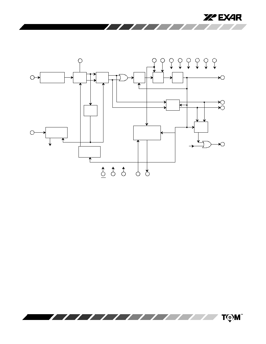
system. Figure 1 shows the block diagram of the device.
The XRT7295AT device is manufactured using linear
CMOS technology. The XRT7295AT is available in a
20-pin plastic SOJ package for surface mounting.
Two versions of the chip are available, one is for either
DS3 or STS-1 operation (the XRT7295AT, this data
sheet), and the other is for E3 operation (the XRT7295AE,
refer to the XRT7295AE data sheet). Both versions are
pin compatible.
For either DS3 or STS-1, an input reference clock at
44.736MHz or 51.84MHz provides the frequency
reference for the device.
ORDERING INFORMATION
Part No.
Package
Operating
Temperature Range
XRT7295ATIW
20 Lead 300 Mil JEDEC SOJ
-40°C to + 85°C
XRT7295AT
2
Rev.1.20
BLOCK DIAGRAM
Figure 1. Block Diagram
Attenuator
AGC
Peak
Detector
Slicers
Phase
Detector
Loop
Filter
VCO
Digital
LOS
Detector
Analog
LOS
Frequency Phase
Aquisition Circuit
Equalizer
Tuning Ckt.
Analog
LOS
Gain &
Equalizer
2
R
IN
18
4
5
20
1
11
9
12
10
16
15
7
19
17
3
6
13
8
14
REQB
LOSTHR
ICT
TMC1 TMC2
EXCLK RLOL
RLOS
RNDATA
RPDATA
RCLK
LPF1 LPF2 V
DD
A GNDA V
DD
D GNDD V
DD
C GNDC
Retimer
XRT7295AT
3
Rev.1.20
PIN CONFIGURATION
V
DD
A
LOSTHR
REQB
ICT
GNDA
R
IN
TMC1
LPF1
RPDATA
RNDATA
RCLK
EXCLK
LPF2
TMC2
RLOS
RLOL
V
DD
C
GNDD
V
DD
D
GNDC
20 Lead SOJ (Jedec, 0.300")
20
1
11
10
2
3
4
5
6
7
15
14
13
12
17
16
8
9
19
18
PIN DESCRIPTION
Pin #
Symbol
Type
Description
1
GNDA
Analog Ground.
2
R
IN
I
Receive Input.
Analog receive input. This pin is internally biased at about 1.5V in series
with 50 kW.
3,6
TMC1-TMC2
I
Test Mode Control 1 and 2
. Internal test modes are enabled within the device by using
TMC1 and TMC2. Users must tie these pins to the ground plane.
4,5
LPF1-LPF2
I
PLL Filter 1 and 2
. An external capacitor (0.1mF ±20%) is connected between these pins.
7
RLOS
O
Receive Loss-of-signal.
This pin is set high on loss of the data signal at the receive input.
(See Table 6)
8
RLOL
O
Receive PLL Loss-of-lock.
This pin is set high on loss of PLL frequency lock.
9
GNDD
Digital Ground for PLL Clock
. Ground lead for all circuitry running synchronously with
PLL clock.
10
GNDC
Digital Ground for EXCLK
. Ground lead for all circuitry running synchronously with
EXCLK.
11
V
DD
D
5V Digital Supply (±10%) for PLL Clock. Power for all circuitry running synchronously
with PLL clock.
12
V
DD
C
5V Digital Supply (±10%) for EXCLK. Power for all circuitry running synchronously with
EXCLK.
13
EXCLK
I
External Reference Clock
. A valid DS3 (44.736MHz ±100ppm) or STS-1 (51.84MHz +
100ppm) clock must be provided at this input. The duty cycle of EXCLK, referenced to V
DD
/2 levels, must be within 40% - 60% with a minimum rise and fall time (10% to 90%) of 5ns.
14
RCLK
O
Receive Clock
. Recovered clock signal to the terminal equipment.
15
RNDATA
O
Receive Negative Data
. Negative pulse data output to the terminal equipment. (See
Figure 11.
)
16
RPDATA
O
Receive Positive Data
. Positive pulse data output to the terminal equipment. (See
Figure 11
)
17
ICT
I
In-circuit Test Control (Active-low)
. If ICT is forced low, all digital output pins (RCLK,
RPDATA, RNDATA, RLOS, RLOL) are placed in a high-impedance state to allow for in-cir-
cuit testing. There is an internal pull-up on this pin.
18
REQB
I
Receive Equalization Bypass
. A high on this pin bypasses the internal equalizer. A low
places the equalizer in the data path.
19
LOSTHR
I
Loss-of-signal Threshold Control
. The voltage forced on this pin controls the input loss-
of-signal threshold. Three settings are provided by forcing GND, V
DD
/2, or V
DD
. This pin
must be set to the desired level upon power-up and should not be changed during opera-
tion.
20
V
DD
A
5V Analog Supply (±10%).
XRT7295AT
4
Rev.1.20
ELECTRICAL CHARACTERISTICS
Test Conditions: T
A
= -40°C to +85°C, V
DD
= 5V + 10%
Typical Values are for V
DD
= 5.0 V, 25°C, and Random Data. Maximum Values are for V
DD
= 5.5V all 1s Data.
Symbol
Parameter
Min.
Typ.
Max.
Unit
Condition
Electrical Characteristics
I
DD
Power Supply Current
DS3
82
79
106
103
mA
mA
REQB=0
REQB=1
STS--1
87
83
111
108
mA
mA
REQB=0
REQB=1
Logic Interface Characteristics
Input Voltage
V
IL
Low
GNDD
0.5
V
V
IH
High
V
DD
D-0.5
V
DD
D
V
Output Voltage
V
OL
Low
GNDD
0.4
V
-5.0mA
V
OH
High
V
DD
D-0.5
V
DD
D
V
5.0mA
C
I
Input Capacitance
10
pF
C
L
Load Capacitance
10
pF
I
L
Input Leakage
-10
10
mA
-0.5 to V
DD
+ 0.5V
(all input pins except 2, 3, 4, 5, 6,
17, 18, & 19)
20
500
mA
0 V (pin 17)
10
100
mA
V
DD
(pin 2)
-50
-5
mA
GNDD (pin 2)
Specifications are subject to change without notice
ABSOLUTE MAXIMUM RATINGS
Power Supply
-0.5V to +6.5V
. . . . . . . . . . . . . . . . . . . . .
Storage Temperature
-40°C to +125°C
. . . . . . . . . . . .
Power Dissipation
700 mW
. . . . . . . . . . . . . . . . . . . . . . .
XRT7295AT
5
Rev.1.20
XR-T7296
Transmitter
Cross
Connect
Frame
DSX-3
or STSX-1
Type 728A
Coaxial Cable
0-450 ft.
0-450 ft.
System A
XRT7295AT
System B
Figure 2. Application Diagram
Receiver
SYSTEM DESCRIPTION
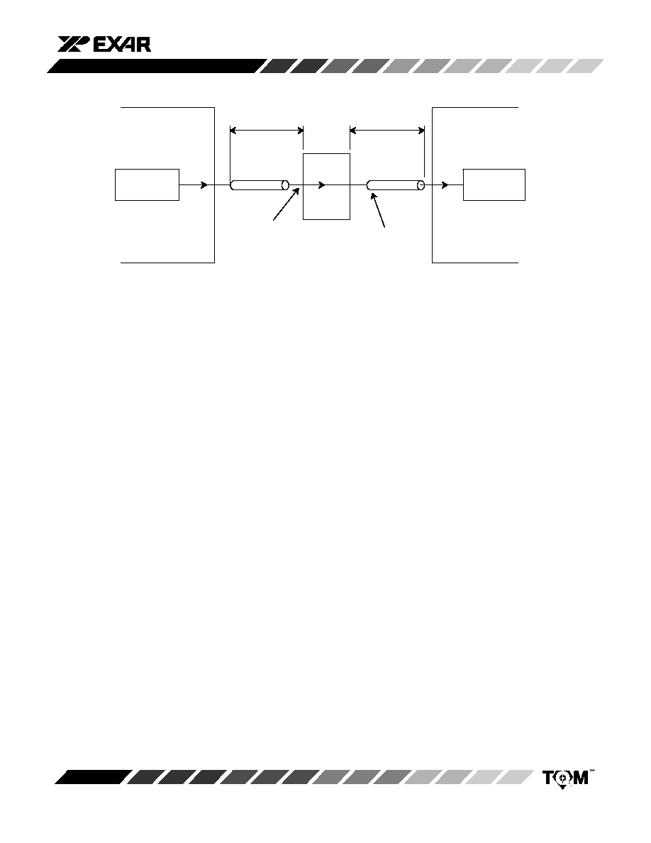
Receive Path Configurations
In the receive signal path (see Figure 1), the internal
equalizer can be included by setting REQB = 0 or
bypassed by setting REQB = 1. The equalizer bypass
option allows easy interfacing of the XRT7295AT device
into systems already containing external equalizers.
Figure 3
illustrates the receive path options.
In Case 1 of Figure 3, the signal from the DSX-3
cross-connect feeds directly into R
IN
. In this mode, the
user should set REQB = 0, engaging the equalizer in the
data path.
In Case 2 of Figure 3, external line build-out (LBO) and
equalizer networks precede the XRT7295AT device. In
this mode, the signal at R
IN
is already equalized, and the
on-chip filters should be bypassed by setting REQB=1.
In applications where the XRT7295AT device is used to
monitor DS3 transmitter outputs directly, the receive
equalizer should be bypassed.
Maximum input amplitude under all conditions is 850mV
pk.