
XR-T7295
...the analog plus company
TM
DS3/Sonet STS-1
Integrated Line Receiver
Rev. 1.05
E
1992
EXAR Corporation, 48720 Kato Road, Fremont, CA 94538
z
(510) 668-7000
z
FAX (510) 668-7017
1
June 1997-3
FEATURES
D
Fully Integrated Receive Interface for DS3 and
STS-1 Rate Signals
D
Integrated Equalization (Optional) and Timing
Recovery
D
Loss-of-Signal and Loss-of-Lock Alarms
D
Variable Input Sensitivity Control
D
5V Power Supply
D
Pin Compatible with XR-T7295E
D
Companion Device to T7296 Transmitter
APPLICATIONS
D
Interface to DS-3 Networks
D
Digital Cross-Connect Systems
D
CSU/DSU Equipment
D
PCM Test Equipment
D
Fiber Optic Terminals
GENERAL DESCRIPTION
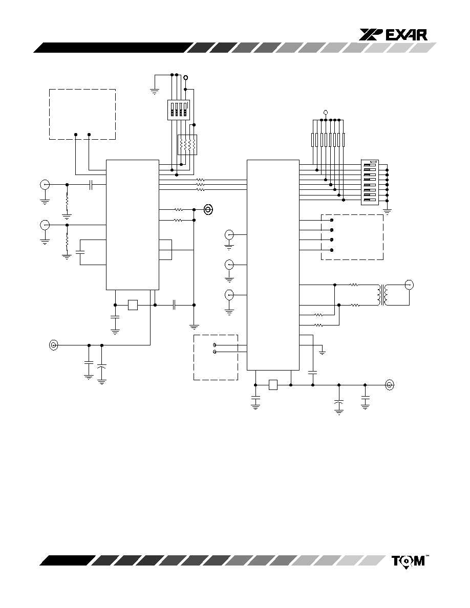
The XR-T7295 DS3/SONET STS-1 integrated line
receiver is a fully integrated receive interface that
terminates a bipolar DS3 (44.736Mbps) or Sonet STS-1
(51.84Mbps) signal transmitted over coaxial cable. (See
Figure 13).
The device also provides the functions of receive
equalization (optional), automatic-gain control (AGC),
clock-recovery and data retiming, loss-of-signal and
loss-of-frequency-lock detection. The digital system
interface is dual-rail, with received positive and negative
1s appearing as unipolar digital signals on separate
output leads. The on-chip equalizer is designed for cable
distances of 0 to 450ft. from the cross-connect frame to
the device. The receive input has a variable input
sensitivity control, providing three different sensitivity
settings, to adapt longer cables. High input sensitivity
allows for significant amounts of flat loss within the
system.
Figure 1 shows the block diagram of the device.
The XR-T7295 device is manufactured using linear
CMOS technology. The XR-T7295 is available in either a
20-pin plastic DIP or 20-pin plastic SOJ package for
surface mounting.
Two versions of the chip are available, one is for either
DS3 or STS-1 operation (the XR-T7295, this data sheet),
and the other is for E3 operation (the XR-T7295E, refer to
the XR-T7295E data sheet). Both versions are pin
compatible.
For either DS3 or STS-1, an input reference clock at
44.736MHz or 51.84MHz provides the frequency
reference for the device.
ORDERING INFORMATION
Part No.
Package
Operating
Temperature Range
XR-T7295IP
20 Lead 300 Mil PDIP
-40
�
C to + 85
�
C
XR-T7295IW
20 Lead 300 Mil JEDEC SOJ
-40
�
C to + 85
�
C

XR-T7295
2
Rev. 1.05
BLOCK DIAGRAM
Figure 1. Block Diagram
�����
�����
�����
���
���
���
���
���
���
���
���
���
�����
�����
�����
�����
�����
������
������
������
���
���
���
���
���
��
��
��
���
���
���
���
���
���
��
��
��
��
��
��
�
�
�
�
��
��
�
�
�
�
��
��
�
�
�
�
�
��
��
��
��
�
�
��
��
��
��
�
�
��
Attenuator
AGC
Peak
Detector
Slicers
Phase
Detector
Loop
Filter
VCO
Digital
LOS
Detector
Analog
LOS
Frequency Phase
Aquisition Circuit
Equalizer
Tuning Ckt.
Analog
LOS
Gain &
Equalizer
2
R
IN
18
4
5
20
1
11
9
12
10
16
15
7
19
17
3
6
13
8
14
REQB
LOSTHR
ICT
TMC1
TMC2
EXCLK
RLOL
RLOS
RNDATA
RPDATA
RCLK
LPF1
LPF2
V
DD
A GNDA V
DD
D GNDD V
DD
C GNDC
Retimer

XR-T7295
3
Rev. 1.05
PIN CONFIGURATION
V
DD
A
LOSTHR
REQB
ICT
RPDATA
RNDATA
RCLK
EXCLK
GNDA
R
IN
TMC1
LPF1
LPF2
TMC2
RLOS
RLOL
V
DD
C
GNDD
V
DD
D
GNDC
20 Lead PDIP (0.300")
1
2
3
4
5
6
7
8
9
10
20
19
18
17
16
15
14
13
12
11
V
DD
A
LOSTHR
REQB
ICT
GNDA
R
IN
TMC1
LPF1
RPDATA
RNDATA
RCLK
EXCLK
LPF2
TMC2
RLOS
RLOL
V
DD
C
GNDD
V
DD
D
GNDC
20 Lead SOJ (Jedec, 0.300")
20
1
11
10
2
3
4
5
6
7
15
14
13
12
17
16
8
9
19
18
PIN DESCRIPTION
Pin #
Symbol
Type
Description
1
GNDA
Analog Ground.
2
R
IN
I
Receive Input. Analog receive input. This pin is internally biased at about 1.5V in series
with 50 k
.
3,6
TMC1-TMC2
I
Test Mode Control 1 and 2. Internal test modes are enabled within the device by using
TMC1 and TMC2. Users must tie these pins to the ground plane.
4,5
LPF1-LPF2
I
PLL Filter 1 and 2. An external capacitor (0.1
�
F
$
20%) is connected between these pins.
7
RLOS
O
Receive Loss-of-signal. This pin us set high on loss of the data signal at the receive input.
(See
Table 7)
8
RLOL
O
Receive PLL Loss-of-lock. This pin is set high on loss of PLL frequency lock.
9
GNDD
Digital Ground for PLL Clock. Ground lead for all circuitry running synchronously with
PLL clock.
10
GNDC
Digital Ground for EXCLK. Ground lead for all circuitry running synchronously with
EXCLK.
11
V
DD
D
5V Digital Supply (
$
10%) for PLL Clock. Power for all circuitry running synchronously
with PLL clock.
12
V
DD
C
5V Digital Supply (
$
10%) for EXCLK. Power for all circuitry running synchronously with
EXCLK.
13
EXCLK
I
External Reference Clock. A valid DS3 (44.736MHz
$
100ppm) or STS-1 (51.84MHz +
100ppm) clock must be provided at this input. The duty cycle of EXCLK, referenced to V
DD
/2 levels, must be within 40% - 60% with a minimum rise and fall time (10% to 90%) of 5ns.
14
RCLK
O
Receive Clock. Recovered clock signal to the terminal equipment.
15
RNDATA
O
Receive Negative Data. Negative pulse data output to the terminal equipment. (See
Figure 11.)
16
RPDATA
O
Receive Positive Data. Positive pulse data output to the terminal equipment. (See
Figure 11)
17
ICT
I
In-circuit Test Control (Active-low). If ICT is forced low, all digital output pins (RCLK,
RPDATA, RNDATA, RLOS, RLOL) are placed in a high-impedance state to allow for in-cir-
cuit testing. There is an internal pull-up on this pin.
18
REQB
I
Receive Equalization Bypass. A high on this pin bypasses the internal equalizer. A low
places the equalizer in the data path.
19
LOSTHR
I
Loss-of-signal Threshold Control. The voltage forced on this pin controls the input loss-
of-signal threshold. Three settings are provided by forcing GND, V
DD
/2, or V
DD
. This pin
must be set to the desired level upon power-up and should not be changed during opera-
tion.
20
V
DD
A
5V Analog Supply (
$
10%).

XR-T7295
4
Rev. 1.05
ELECTRICAL CHARACTERISTICS
Test Conditions: T
A
= -40
�
C to +85
�
C, V
DD
= 5V
$
10%
Typical Values are for V
DD
= 5.0 V, 25
�
C, and Random Data. Maximum Values are for V
DD
= 5.5V all 1s Data.
Symbol
Parameter
Min.
Typ.
Max.
Unit
Condition
Electrical Characteristics
I
DD
Power Supply Current
DS3
REQB = 0
82
106
mA
REQB = 1
79
103
mA
STS-1
REQB = 0
87
111
mA
REQB = 1
83
108
mA
Logic Interface Characteristics
Input Voltage
V
IL
Low
GNDD
0.5
V
V
IH
High
V
DD
D-
0.5
V
DD
D
V
Output Voltage
V
OL
Low
GNDD
0.4
V
-5.0mA
V
OH
High
V
DD
D-
0.5
V
DD
D
V
5.0mA
C
I
Input Capacitance
10
pF
C
L
Load Capacitance
10
pF
I
L
Input Leakage
-10
10
�
A
-0.5 to V
DD
+ 0.5V
(all input pins except 2 and 17)
20
500
�
A
0 V (pin 17)
10
100
�
A
V
DD
(pin 2)
-50
-5
�
A
GNDD (pin 2)
Specifications are subject to change without notice
ABSOLUTE MAXIMUM RATINGS
Power Supply
-0.5V to +6.5V
. . . . . . . . . . . . . . . . . . . . .
Storage Temperature
-40
�
C to +125
�
C
. . . . . . . . . . . .
Power Dissipation
700 mW
. . . . . . . . . . . . . . . . . . . . . . .

XR-T7295
5
Rev. 1.05
�
����
����
����
�����
�����
�����
�
����
����
����
����
����
XR-T7296
Transmitter
Cross
Connect
Frame
DSX-3
or STSX-1
Type 728A
Coaxial Cable
0-450 ft.
0-450 ft.
System A
XR-T7295
System B
Figure 2. Application Diagram
Receiver
SYSTEM DESCRIPTION
Receive Path Configurations
In the receive signal path (see
Figure 1), the internal
equalizer can be included by setting REQB = 0 or
bypassed by setting REQB = 1. The equalizer bypass
option allows easy interfacing of the XR-T7295 device
into systems already containing external equalizers.
Figure 3 illustrates the receive path options.
In Case 1 of
Figure 3, the signal from the DSX-3
cross-connect feeds directly into R
IN
. In this mode, the
user should set REQB = 0, engaging the equalizer in the
data path.
Table 1 and the following sections describe the
receive signal requirements.
In Case 2 of
Figure 3, external line build-out (LBO) and
equalizer networks precede the XR-T7295 device. In this
mode, the signal at R
IN
is already equalized, and the
on-chip filters should be bypassed by setting REQB=1.
The signal at R
IN
must meet the amplitude limits
described in
Table 1
In applications where the XR-T7295 device is used to
monitor DS3 transmitter outputs directly, the receive
equalizer should be bypassed. Again, the signal at R
IN
must meet the amplitude limits described in
Table 1.
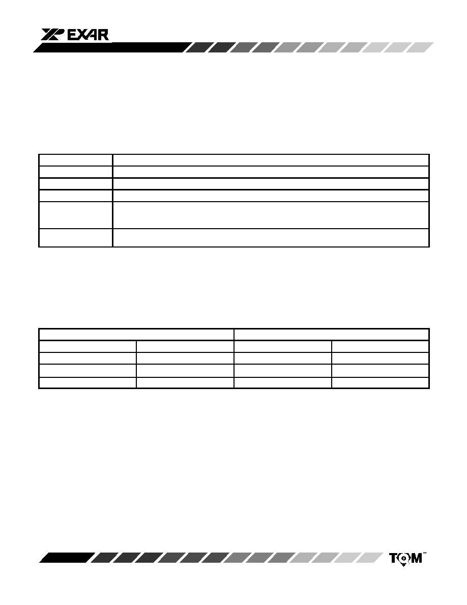
Minimum signals are for SOJ devices. Due to increased
package parasitics, add 3dB to all table values for DIP
devices.
Maximum input amplitude under all conditions is 850mV
pk.
Although system designers typically use power in dBm to
describe input levels, the XR-T7295 responds to peak
input signal amplitude. Therefore, the XR-T7295 input
signal limits are given in mV pk. Conversion factors are as
follows:
At DSX3: 390mV pk
'
0 dBm
At DSX3 + 450 ft. of cable: 310 mV pk
'
0 dBm
Data
Rate
REQB
LOSTHR
Minimum
Signal
Unit
DS3
0
0
80
mV pk
V
DD
/2
60
mV pk
V
DD
40
mV pk
1
0
80
mV pk
V
DD
/2
80
mV pk
V
DD
80
mV pk
STS-1
0
0
110
mV pk
V
DD
/2
80
mV pk
V
DD
60
mV pk
1
0
110
mV pk
V
DD
/2
110
mV pK
V
DD
110
mV pk
Table 1. Receive Input Signal Amplitude
Requirements

XR-T7295
6
Rev. 1.05
Figure 3. Receiver Configurations
���
���
���
���
���
����
����
����
����
����
����
����
������
������
������
������
������
���
���
���
���
���
���
���
���
������
������
������
������
������
���
���
���
Existing
Off-chip
Networks
0-450 ft.
CASE 2:
D
S
X
225 ft.
LBO
Closed For
225-450 ft.
Of Cable
75
0.01
�
F
0.1
�
F
R
IN
REQB
LPF1
LPF2
XR-T7295
CASE 1:
0-450 ft.
R
IN
XR-T7295
REQB
D
S
X
0.01
�
F
75
0.1
�
F
LPF1
LPF2
1
0
Fixed
Equalizer
����
����
����
����
����
����
����
XR-T7295
7
Rev. 1.05
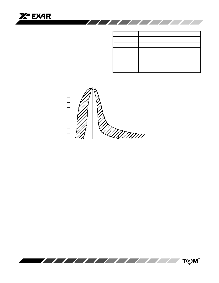
DS3 SIGNAL REQUIREMENTS AT THE DSX
Pulse characteristics are specified at the DSX-3, which is
an interconnection and test point referred to as the
cross-connect (see
Figure 2.) The cross-connect exists
at the point where the transmitted signal reaches the
distribution frame jack.
Table 2 lists the signal
requirements. Currently, two isolated pulse template
requirements exist: the ACCUNET T45 pulse template
(see
Table 3 and Figure 4) and the G.703 pulse template
(see
Table 4 and Figure 5). Table 3 and Table 5 give the
associated boundary equations for the templates. The
XR-T7295 correctly decodes any transmitted signal that
meets one of these templates at the cross-connect.
Parameter
Specification
Line Rate
44.736 Mbps
20 ppm
Line Code
Bipolar with three-0 substitution (B3ZS)
Test Load
75
5%
Pulse Shape
An isolated pulse must fit the template in
Figure 4 or Figure 5.
1
The pulse amplitude may be scaled by
a constant factor to fit the template. The pulse amplitude must be between 0.36vpk and 0.85vpk,
measured at the center of the pulse.
Power Levels
For and all 1s transmitted pattern, the power at 22.368
$
0.002MHz must be -1.8 to +5.7dBm, and
the power at 44.736
$
0.002MHz must be -21.8dBm to -14.3dBm.
2, 3
Notes
1
The pulse template proposed by G.703 standards is shown in Figure 5 and specified in Table 4. The proposed G.703 standards
further state that the voltage in a time slot containing a 0 must not exceed
$
5% of the peak pulse amplitude, except for the residue
of preceding pulses.
2
The power levels specified by the proposed G.703 standards are identical except that the power is to be measured in 3kHz bands.
3
The all 1s pattern must be a pure all 1s signal, without framing or other control bits.
Table 2. DSX-3 Interconnection Specification
Lower Curve
Upper Curve
Time
Equation
Time
Equation
T
-0.36
0
T
-0.68
0
-0.36
T
+0.28
0.5 1+sin
/2
[
1+T/0.18
]
-0.68
T
+0.36
0.5 1+sin
/2
[
1+T/0.34
]
0.28
T
0.11e
-3.42(T-0.3)
0.36
T
0.05 + 0.407e
-1.84(T-0.36)
Table 3. DSX-3 Pulse Template Boundaries for ACCUNET T45 Standards (See
Figure 4.)

XR-T7295
8
Rev. 1.05
Figure 4. DSX-3 Isolated Pulse Template for ACCUNET T45 Standards
���������������
���������������
���������������
���������������
���������������
���������������
���������������
���������������
���������������
���������������
1.0
0.8
0.6
0.4
0.2
0
-1.0
-0.5
0
0.5
1.0
1.5
2.0
Time Slots - Normalized To Peak Location
��������������
��������������
��������������
��������������
��������������
��������������
��������������
��������������
��������������
��������������
��������������
��������������
��������������
��������������
��������������
��������������
��������������
��������������
��������������
��������������
��������
��������
��������
��������
��������
��������
��������
��������
��������
��������
��������
��������
��������
��������
��������
��������
��������
��������
��������
��������
Normalized Amplitude
Lower Curve
Upper Curve
Time
Function
Time
Function
T
-0.36
0
T
-0.65
0
-0.36
T
+0.28
0.5 1+sin
/2
[
1+T/0.18
]
-0.65
T
0
1.05 1-e
-4.6(T+0.65)
0.28
T
0.11e
-3.42(T-0.3)
0
T
0.36
0.5 1+sin
/2
[
1+T/0.34
]
0.36
T
0.05+0.407e
-1.84(T-0.36)
Table 4. DSX-3 Pulse Template Boundaries for G.703 Standards (See
Figure 5)
Figure 5. DSX-3 Isolated Pulse Template for G.703 Standards
���������������
���������������
���������������
���������������
���������������
���������������
���������������
���������������
���������������
���������������
���������������
1.0
0.8
0.6
0.4
0.2
0
-1.0
-0.5
0
0.5
1.0
1.5
2.0
Time Slots - Normalized To Peak Location
��������������
��������������
��������������
��������������
��������������
��������������
��������������
��������������
��������������
��������������
��������������
��������������
��������������
��������������
��������������
��������������
��������������
��������������
��������������
��������������
��������������
��������������
�������
�������
�������
�������
�������
�������
�������
�������
�������
�������
�������
�������
�������
�������
�������
�������
�������
�������
�������
�������
Normalized Amplitude
XR-T7295
9
Rev. 1.05
STS-1 SIGNAL REQUIREMENTS AT THE STSX
For STS-1 operation, the cross-connect is referred at the
STSX-1.
Table 5 lists the signal requirements at the
STSX-1. Instead of the DS3 isolated pulse template, an
eye diagram mask is specified for STS-1 operation
(TA-TSY-000253). The XR-T7295 correctly decodes any
transmitted signal that meets the mask shown in
Figure 6
at the STSX-1.
Parameter
Specification
Line Rate
51.84 Mbps
Line Code
Bipolar with three-0 substitution (B3ZS)
Test Load
75
$
5%
Power Levels
A wide-band power level measurement
at the STSX-1 interface using a low-pass
filter with a 3dB cutoff frequency of at
least 200MHz is within -2.7 dBm and 4.7
dBm.
Table 5. STSX-1 Interconnection Specification
Figure 6. STSX-1 Isolated Pulse Template for Bellcore TA-TSY-000253
���������������
���������������
���������������
���������������
���������������
���������������
���������������
���������������
���������������
���������������
���������������
1.0
0.8
0.6
0.4
0.2
0
-1.0
-0.5
0
0.5
1.0
1.5
2.0
Time Slots - Normalized To Peak Location
��������������
��������������
��������������
��������������
��������������
��������������
��������������
��������������
��������������
��������������
��������������
��������������
��������������
��������������
��������������
��������������
��������������
��������������
��������������
��������������
��������������
�������
�������
�������
�������
�������
�������
�������
�������
�������
�������
�������
�������
�������
�������
�������
�������
�������
�������
�������
�������
Normalized Amplitude
LINE TERMINATION AND INPUT CAPACITANCE
The recommended receive termination is shown in
Figure 3 The 75
resistor terminates the coaxial cable
with its characteristic impedance. The 0.01
�
F capacitor
to R
IN
couples the signal into the receive input without
disturbing the internally generated DC bias level present
on R
IN
. The input capacitance at the R
IN
pin is 2.8pF
typical (SOJ package) and 3.6pF typical (DIP package).
LOSS LIMITS FROM THE DSX-3 TO THE RECEIVE
INPUT
The signal at the cross-connect may travel through a
distribution frame, coaxial cable, connector, splitters, and
back planes before reaching the XR-T7295 device. This
section defines the maximum distribution frame and cable
loss from the cross-connect to the XR-T7295 input.
The distribution frame jack may introduce 0.6
$
0.55 dB
of loss. This loss may be any combination of flat or
shaped (cable) loss.
The maximum cable distance between the point where
the transmitted signal exits the distribution frame jack and
the XR-T7295 device is 450 ft. (see
Figure 2.) The
coaxial cable (Type 728A) used for specifying this
distance limitation has the loss and phase characteristics
shown in
Figure 7 and Figure 8. Other cable types also
may be acceptable if distances are scaled to maintain
cable loss equivalent to Type 728A cable loss.
TIMING RECOVERY
External Loop Filter Capacitor
Figure 3 shows the connection to an external 0.1
�
F
capacitor at the LPF1/LPF2 pins. This capacitor is part of
the PLL filter. A non-polarized, low-leakage capacitor
should be used. A ceramic capacitor with the value 0.1
�
F
$
20% is acceptable.

XR-T7295
10
Rev. 1.05
OUTPUT JITTER
The total jitter appearing on the RCLK output during
normal operation consists of two components. First,
some jitter appears on RCLK because of jitter on the
incoming signal. (The next section discusses the jitter
transfer characteristic, which describes the relationship
between input and output jitter.) Second, noise sources
within the XR-T7295 device and noise sources that are
coupled into the device through the power supplies and
data pattern dependent jitter due to misequalization of the
input signal, all create jitter on RCLK. The magnitude of
this internally generated jitter is a function of the PLL
bandwidth, which in turn is a function of the input 1s
density. For higher 1s density, the amount of generated
jitter decreases. Generated jitter also depends on the
quality of the power supply bypassing networks used.
Figure 12 shows the suggested bypassing network, and
Table 6 lists the typical generated jitter performance.
Figure 7. Loss Characteristic of 728A
Coaxial Cable (450 ft.)
Figure 8. Phase Characteristic of 728A
Coaxial Cable (450 ft.)
������������
������������
������������
������������
������������
������������
������������
������������
������������
������������
������������
������������
������������
������������
������������
������������
������������
������������
������������
������������
������������
������������
������������
������������
������������
������������
������������
������������
������������
������������
������������
������������
������������
������������
������������
������������
12
10
8
6
4
2
0
1.0
2.0
5.0 10
20
50
100
Frequency (MHz)
�������������
�������������
�������������
�������������
�������������
�������������
�������������
�������������
�������������
�������������
�������������
�������������
�������������
�������������
�������������
�������������
�������������
�������������
�������������
�������������
�������������
�������������
�������������
�������������
�������������
�������������
�������������
�������������
�������������
�������������
100
80
60
40
20
0
1.0
2.0
5.0
10
20
50
100
Frequency (MHz)
Loss (dB)
Phase (Degree)
JITTER TRANSFER CHARACTERISTIC
The jitter transfer characteristic indicates the fraction of
input jitter that reaches the RCLK output as a function of
input jitter frequency.
Table 6 shows Important jitter
transfer characteristic parameters.
Figure 9 also shows a
typical characteristic, with the operating conditions as
described in
Table 6. Although existing standards do not
specify jitter transfer characteristic requirements, the
XR-T7295 information is provided here to assist in
evaluation of the device.
Parameter
Typ
Max
Unit
Generated Jitter
1
All 1s pattern
1.0
ns peak-to-peak
Repetitive "100"
pattern
1.5
ns peak-to-peak
Jitter Transfer
Characteristic
2
Characteristic
Peaking
0.05
0.1
dB
f 3dB
0 05
205
0
d
kHz
Notes
1
Repetitive input data pattern at nominal DSX-3 level with
V
DD
= 5V T
A
= 25
�
C.
2
Repetitive "100 " input at nominal DSX-3 level with V
DD
= 5V,
T
A
= 25
�
C.
Table 6. Generated Jitter and Jitter Transfer
Characteristics

XR-T7295
11
Rev. 1.05
JITTER ACCOMMODATION
Under all allowable operating conditions, the jitter
accommodation of the XR-T7295 device exceeds all
system requirements for error-free operation
(BER<1E
-9
). The typical (V
DD
= 5V, T = 25
�
C, DSX-3
nominal signal level) jitter accommodation for the
XR-T7295 is shown in
Figure 10.
FALSE-LOCK IMMUNITY
False-lock is defined as the condition where a PLL
recovered clock obtains stable phase-lock at a frequency
not equal to the incoming data rate. The XR-T7295
device uses a combination frequency/phase-lock
architecture to prevent false-lock. An on-chip frequency
comparator continuously compares the EXCLK reference
to the PLL clock. If the frequency difference between the
EXCLK and PLL clock exceeds approximately
$
0.5%,
correction circuitry forces re-acquisition of the proper
frequency and phase.
ACQUISITION TIME
If a valid input signal is assumed to be already present at
R
IN
, the maximum time between the application of device
power and error-free operation is 20ms. If power has
already been applied, the interval between the application
of valid data (or the action of valid data following a loss of
signal) and error-free operation is 4ms.
LOSS-OF-LOCK DETECTION
As stated above, the PLL acquisition aid circuitry monitors
the PLL clock frequency relative to the EXCLK frequency.
The RLOL alarm is activated if the difference between the
PLL clock and the EXCLK frequency exceeds
approximately
$
0.5%.
This will not occur until at least 250 bit periods after loss of
input data.
Figure 9. Typical PLL Jitter Transfer
Characteristic
������������
������������
������������
������������
������������
������������
������������
������������
������������
����������
����������
����������
����������
����������
����������
����������
����������
����������
����������
����������
����������
����������
����������
����������
����������
1
0
-5
-4
-3
-2
-1
100
500 1K
5K 10K
50K100K
500K
PEAK = 0.05dB
f3dB = 205kHz
Frequency (Hz)
Magnitude Response (dB)
����������������������
����������������������
����������������������
����������������������
����������������������
����������������������
����������������������
����������������������
����������������������
����������������������
����������������������
1 10 100 1K 10K 100K 1000K
40
10
1.0
0.1
�����
�����
XR-T7295 Typical
PUB 54014
G.824
����
����
TR-TSY-000499
Category 1
����
����
TR-TSY-000499
Category 2
��������
��������
��������
��������
��������
��������
��������
��������
��������
5k 10
10k 5
60k 1
300k 0.5
1M 0.4
XR-T7295 Typical
Sinewave Jitter Frequency (Hz)
Figure 10. Input Jitter Tolerance at DSX-3 Level
Jitter
Frequency
(Hz)
Jitter
Amplitude
(U.I.)
Peak-Peak Sinewave Jitter (U.I.)

XR-T7295
12
Rev. 1.05
A high RLOL output indicates that the acquisition circuit is
working to bring the PLL into proper frequency lock.
RLOL remains high until frequency lock has occurred;
however, the minimum RLOL pulse width is 32 clock
cycles.
PHASE HITS
In response to a phase hit in the input data, the XR-T7295
returns to error free operation in less than 2ms. During
the requisition time, RLOS may temporarily be indicated.
LOSS-OF-SIGNAL DETECTION
Figure 1 shows that analog and digital methods of
loss-of-signal (LOS) detection are combined to create the
RLOS alarm output. RLOS is set if either the analog or
digital detection circuitry indicates LOS has occurred.
ANALOG DETECTION
The analog LOS detector monitors the peak input signal
amplitude. RLOS makes a high-to-low transition (input
signal regained) when the input signal amplitude exceeds
the loss-of signal threshold defined in
Table 7. The RLOS
low-to-high transition (input signal loss) occurs at a level
typically 1.0 dB below the high-to-low transition level. The
hysteresis prevents RLOS chattering. Once set, the
RLOS alarm remains high for at least 32 clock cycles,
allowing for system detection of a LOS condition without
the use of an external latch.
To allow for varying levels of noise and crosstalk in
different applications, three loss-of-signal threshold
settings are available using the LOSTHR pin. Setting
LOSTHR = V
DD
provides the lowest loss-of-signal
threshold; LOSTHR = V
DD
/2 (can be produced using two
50 k
$
10% resistors as a voltage divider between
V
DD
D and GNDD) provides an intermediate threshold;
and LOSTHR = GND provides the highest threshold. The
LOSTHR pin must be set to its desired value at power-up
and must not be changed during operation.
DIGITAL DETECTION
In addition to the signal amplitude monitoring of the
analog LOS detector, the digital LOS detector monitors
the recovered data 1s density. The RLOS alarm goes
high if 160
$
32 or more consecutive 0s occur in the
receive data stream. The alarm goes low when at least
ten 1s occur in a string of 32 consecutive bits. This
hysteresis prevents RLOS chattering and guarantees a
minimum RLOS pulse width of 32 clock cycles. Note,
however, that RLOS chatter can still occur. When
REQB=1, input signal levels above the analog RLOS
threshold can still be low enough to result in a high bit error
rate. The resultant data stream (containing) errors can
temporarily activate the digital LOS detector, and RLOS
chatter can occur. Therefore, RLOS should not be used
as a bit error rate monitor.
RLOS chatter can also occur when RLOL is activated
(high).

XR-T7295
13
Rev. 1.05
Data
Rate
REQB
LOSTHR
Min.
Threshold
Max.
Threshold
Unit
DS3
0
0
60
220
mV pk
V
DD
/2
40
145
mV pk
V
DD
25
90
mV pk
1
0
45
175
mV pk
V
DD
/2
30
115
mV pk
V
DD
20
70
mV pk
STS-1
0
0
75
275
mV pk
V
DD
/2
50
185
mV pk
V
DD
30
115
mV pk
1
0
55
220
mV pk
V
DD
/2
35
145
mV pk
V
DD
25
90
mV pk
Notes
- Lower threshold is 1.5 dB below upper threshold.
- The RLOS alarm is an indication of the presence of an input signal, not a bit error rate indication. Table 1 gives the minimum
input amplitude needed for error free operation (BER < 1e-
9
) Independent of the RLOS state, the device will attempt to recover
correct timing data. The RLOS low-to-high transition typically occurs 1dB below the high to low transition.
Table 7. Analog Loss-of-Signal Thresholds
RECOVERED CLOCK AND DATA TIMING
Table 8 and Figure 11 summarize the timing relationships
between the logic signals RCLK, RPDATA, and RNDATA.
The duty cycle is referenced to V
DD
/2 threshold level.
RPDATA and RNDATA change on the rising edge of
RCLK and are valid during the falling edge of RCLK. A
positive pulse at R
IN
creates a high level on RPDATA and
a low level on RNDATA. A negative pulse at the input
creates a high level on RNDATA and a low level on
RPDATA, and a received zero produces low levels on
both RPDATA and RNDATA.
IN-CIRCUIT TEST CAPABILITY
When pulled low, the ICT pin forces all digital output
buffers (RCLK, RPDATA, RNDATA, RLOS, RLOL pins) to
be placed in a high output impedance state. This feature
allows in-circuit testing to be done on neighboring devices
without concern for XR-T7295 device buffer damage. An
internal pull-up device (nominally 50k
) is provided on
this pin therefore, users can leave this pin unconnected
for normal operation. Test equipment can pull ICT low
during in-circuit testing without damaging the device.
This is the only pin for which internal pull-up/pull-down is
provided.

XR-T7295
14
Rev. 1.05
TIMING CHARACTERISTICS
Test Conditions: All Timing Characteristics are Measrured with 10pF Loading, -40
�
C
T
A
+85
�
C, V
DD
=
5V
$
10%
Symbol
Parameter
Min
Typ
Max
Unit
tRCH1RCH2
Clock Rise Time (10% - 90%)
3.5
ns
tRCL2RCL1
Clock Fall Time (10% - 90%)
2.5
ns
tRDVRCL
Receive Data Set-up Time
5.0
ns
tRCLRDX
Receive Data Hold Time
8.5
ns
tRCHRDV
Receive Propagation Delay
1
0.6
3.7
ns
Clock Duty Cycle
45
50
55
%
Notes
1
The total delay from R
IN
to the digital outputs RPDATA and RNDATA is three and a half RCLK clocks.
Table 8. System Interface Timing Characteristics
Figure 11. Timing Diagram for System Interface
RCLK
RPDATA
OR
RNDATA
(RC)
(RD)
tRCHRDV
tRCL2RCL1
tRCH1RCH2
tRCLRDX
tRDVRCL
BOARD LAYOUT CONSIDERATIONS
Power Supply Bypassing
Figure 12 illustrates the recommended power supply
bypassing network. A 0.1
�
F capacitor bypasses the
digital supplies. The analog supply V
DD
A is bypassed by
using a 0.1
�
F capacitor and a shield bead that removes
significant amounts of high-frequency noise generated by
the system and by the device logic. Good quality,
high-frequency (low lead inductance) capacitors should
be used. Finally, it is most important that all ground
connections be made to a low-impedance ground plane.
Receive Input
The connections to the receive input pin, R
IN
, must be
carefully considered. Noise-coupling must be minimized
along the path from the signal entering the board to the
input pin. Any noise coupled into the XR-T7295 input
directly degrades the signal-to-noise ratio of the input
signal and may degrade sensitivity.
PLL Filter Capacitor
The PLL filter capacitor between pins LPF1 and LPF2
must be placed as close to the chip as possible. The LPF1
and LPF2 pins are adjacent, allowing for short lead
lengths with no crossovers to the external capacitor.
Noise-coupling into the LPF1 and LPF2 pins may
degrade PLL performance.
Handling Precautions
Although protection circuitry has been designed into this
device, proper precautions should be taken to avoid
exposure to electrostatic discharge (ESD) during
handling and mounting.

XR-T7295
15
Rev. 1.05
C4
Sensitive Node
Shield Bead
1
+5V
C6
GNDA
V
DD
A
GNDD
GNDC
V
DD
C
V
DD
D
0.1
�
F
XR-T7295
0.1
�
F
Figure 12. Recommended Power Supply
Bypassing Network
Notes
1
Recommended shield beads are the Fair-Rite
2643000101 or the Fair-Rite 2743019446 (surface
mount).
COMPLIANCE SPECIFICATIONS
D
Compliance with
AT&T Publication 54014, "ACCU-
NET
R
T45 Service Description and Interface Spec-
ifications," June 1987.
D
Compliance with
ANSI Standard T1.102-1989,
"Digital Hierarchy - Electrical Interfaces, " 1989.
D
Compliance with
Compatibility Bulletin 119,
"Interconnection Specification for Digital
Cross-Connects," October 1979.
D
Compliance with
CCITT Recommendations G.703
and G.824, 1988.
D
Compliance with
TR-TSY-000499, "Transport Sys-
tems Generic Requirements (TSGR): Common Re-
quirements," December 1988.
D
Compliance with
TA-TSY-000253, "Synchronous
Optical Network (SONET) Transport System Gener-
ic Criteria," February 1990.
XR-T7295
16
Rev. 1.05
1
5
1
6
1
4
1
3
1
2
1
1
1
0
9
2 1 3 4 5 6 7 8
R22
22K
V
CC
V
CC
L
O
S
T
H
R
1
2
3
4
5
6
7
8
R21
22K
1
2
3
4
8
6
5
S1
SW DIP-4
RLOS
TP
RLOL
TP
RECEIVER
MONITOR
OUTPUTS
RLOL
8
RLOS
7
R
IN
2
EXCLK
13
V
D
D
A
20
V
D
D
C
1
2
V
D
D
D
1
1
GNDD
9
GNDC
10
GNDA
1
REQB
18
14
RNDATA
15
RPDATA
16
TMC1
3
TMC2
6
LPF1
4
LPF2
5
LOSTHR
19
ICT/
17
C2
0.01
�
F
R2
75
R6
75
INPUT
SIGNAL
EXTERNAL
CLOCK
B1
B2
R1
50
R5
50
R8
39
R10
39
R7
39
B5
TCLK
P2
GND
V
D
D
A
V
D
D
D
6
LLOOP
3
RLOOP
2
DS3,STS-1/E3/
4
TAOS
5
ICT/
26
TXLEV
25
ENCODIS
11
DECODIS
12
RCLK
RNDATA
28
RPDATA
27
DMO
18
BPV
13
TNDATA
8
TCLK
9
TPDATA
7
GNDA
21
GNDD
10
MTIP
20
MRING
19
TTIP
23
TRING
22
RCLKO
17
RPOS
16
RNEG
15
RNRZ
14
U2
XR-T7296
RNEG
RCLKO
RPOS
LLOOP
RLOOP
T3/E3
TAOS
TXLEV
ICT
ENCODIS
DECODIS
RECEIVER
1
2
3
4
5
6
7
8
16
15
14
13
12
11
10
9
S2
SW DIP-8
OUTPUTS
R3
36
R4
36
T1
PE65966
B6
TRING
TTIP
R15
270
R16
270
RNRZ
B4
TNDATA
B3
TPDATA
C6
0.1
�
F
C3
0.1
�
F
C4
0.1
�
F
BT1
FERRITE BEAD
FERRITE BEAD # FAIR RITE 2643000101
C7
0.1
�
F
E1
22
�
F
P1
V
CC
RX
TRANSMITER
MONITOR
OUTPUTS
DMO
BPV
C9
0.1
�
F
E2
22
�
F
C8
0.1
�
F
TRANSFORMER # PULSE ENGINEERING
BT2
FERRITE BEAD
C5
0.1
�
F
PE 65966
PE 65967 IN SURFACE MOUNT
V
CC
TX
U1
XR-T7295
7
RCLK
P3
R
E
Q
B
I
C
T
+
+
1
24
Figure 13. Typical Application Schematic

XR-T7295
17
Rev. 1.05
20 LEAD PLASTIC DUAL-IN-LINE
(300 MIL PDIP)
Rev. 1.00
20
1
11
10
D
e
A
1
E
1
E
A
L
Seating
Plane
SYMBOL
MIN
MAX
MIN
MAX
INCHES
A
0.145
0.210
3.68
5.33
A
1
0.015
0.070
0.38
1.78
A
2
0.115
0.195
2.92
4.95
B
0.014
0.024
0.36
0.56
B
1
0.030
0.070
0.76
1.78
C
0.008
0.014
0.20
0.38
D
0.925
1.060
23.50
26.92
E
0.300
0.325
7.62
8.26
E
1
0.240
0.280
6.10
7.11
e
0.100 BSC
2.54 BSC
e
A
0.300 BSC
7.62 BSC
e
B
0.310
0.430
7.87
10.92
L
0.115
0.160
2.92
4.06
0
�
15
�
0
�
15
�
MILLIMETERS
A
2
B
1
B
C
Note: The control dimension is the inch column
e
B
e
A
XR-T7295
18
Rev. 1.05
SYMBOL
MIN
MAX
MIN
MAX
A
0.145
0.200
3.60
5.08
A
1
0.025
---
0.64
---
A
2
0.120
0.140
3.05
3.56
B
0.014
0.020
0.36
0.51
C
0.008
0.013
0.20
0.30
D
0.496
0.512
12.60
13.00
E
0.292
0.300
7.42
7.62
E
1
0.262
0.272
6.65
6.91
e
0.050 BSC
1.27 BSC
H
0.335
0.347
8.51
8.81
R
0.030
0.040
0.76
1.02
INCHES
MILLIMETERS
e
20
11
20 LEAD SMALL OUTLINE J LEAD
(300 MIL JEDEC SOJ)
Rev. 1.00
10
D
E
H
B
A
1
Seating
Plane
Note: The control dimension is the inch column
1
A
2
A
C
R
E
1

XR-T7295
19
Rev. 1.05
Notes

XR-T7295
20
Rev. 1.05
NOTICE
EXAR Corporation reserves the right to make changes to the products contained in this publication in order to im-
prove design, performance or reliability. EXAR Corporation assumes no responsibility for the use of any circuits de-
scribed herein, conveys no license under any patent or other right, and makes no representation that the circuits are
free of patent infringement. Charts and schedules contained here in are only for illustration purposes and may vary
depending upon a user's specific application. While the information in this publication has been carefully checked;
no responsibility, however, is assumed for inaccuracies.
EXAR Corporation does not recommend the use of any of its products in life support applications where the failure or
malfunction of the product can reasonably be expected to cause failure of the life support system or to significantly
affect its safety or effectiveness. Products are not authorized for use in such applications unless EXAR Corporation
receives, in writing, assurances to its satisfaction that: (a) the risk of injury or damage has been minimized; (b) the
user assumes all such risks; (c) potential liability of EXAR Corporation is adequately protected under the circum-
stances.
Copyright 1992 EXAR Corporation
Datasheet June 1997
Reproduction, in part or whole, without the prior written consent of EXAR Corporation is prohibited.