 | –≠–ª–µ–∫—Ç—Ä–æ–Ω–Ω—ã–π –∫–æ–º–ø–æ–Ω–µ–Ω—Ç: XRT7296IP | –°–∫–∞—á–∞—Ç—å:  PDF PDF  ZIP ZIP |

XRT7296
�
�
��
� !" #� $
� %&! '&( ))!*" $ '&( ))!*""
+ *
FEATURES
$,++-
�
�
�
�
./
.
*
�
�
0,+
1 /,�
+/
2�1 �3+�- 4,++
� %
+/
2�1
/
�
5" 6 5!
+/
2�1 4
++/
*78*%%
+/
2�1 7
4,+�* 49:4 /
/
�
/+ 3/; $,/�
+
&< 02
, +-
APPLICATIONS
�
./
. =7 * 7
�2;
>,
�
�+ *
/� -�
?? >,
�
0@
� >,
�
$3
= �/
+
GENERAL DESCRIPTION
1
"%) .,++- �
�
0@
�
. '")@3 ( ')!@3 (
+/�
� / + 3
,
. ��� =7
* '&!@3 ( +
/A+ /3+
1
� / +
�
�1
"%& =7
* "%&
�
�
/
1
"%) /
� ,� /+/; ,+*+ , + �
� @
,+
// � 6
/1/+ -
7
5"
/
�
1
/
49 '( :4 '(
/
.,/� . � � 3
���
� �1
+
/ +
�-
/
//,� + /+,
�1
/1
.
/
/
+ .
A�
+ +
/
4�1
/
/
.,/� / 3
3+
�+- �1,1
A�
+ /�+
�1
/
/� /
3 + +�
�
/�
.+
� ,� ,�
=*/1
,+
1
//,�-
+�
++-
>,
A�
+ /
� . +
>,+B� �
� �1
/*/
/� �
+�
$ -�
+
+
�,3+
*1� �
� 3�1 +/+
�
+ *3/;
3+
2�1 �1
3,+�* + *3/; //,�
1
"%) ,./�,
, 4@=
�
/1+- /;
!* 0
0 =C
/;
1
/
>,
+
&< 2
, +-
/,
A, 2
. "8 '
/,
� .
D
/
�(
ORDERING INFORMATION
Part No.
Package
Operating
Temperature Range
"%)
0
!
) @+ 0
0
* � D !&
"%)
8
! C
@+ C =C
* � D !&
XRT7296
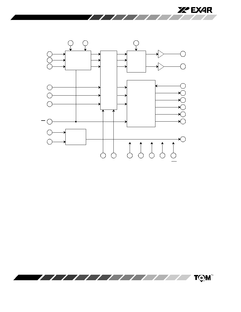
BLOCK DIAGRAM
!
7
%
#
"
0
*
!
%
@
75
@
0
49:4
/
&
)
"
!
7
#
"
0
@�
)
)
==0 ==0
<
57 57 <
4/;
@?
0,+
1
49:4
/
@0
@0
0
75
=
40<
79
75
0=
#=
@=
&
&
= 7=
<
Figure 1. XRT7296 Block Diagram
XRT7296
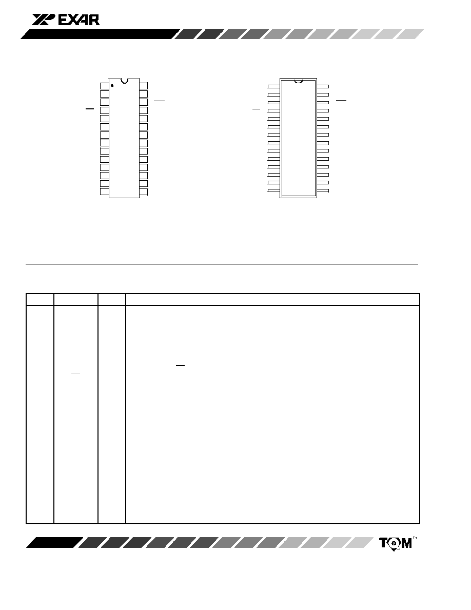
PIN CONFIGURATION
7
0
<
#
==0
==0
*
<
0
75
57
=
<
0
7
@
0
#
@
75
57
@=
7=
#=
=
0=
40<
75
79
28 Lead SOJ (Jedec, 0.300")
!
&
&
)
"
"
)
!
%
%
!
"
)
&
7
0
<
<
0
75
57
#
==0
==0
*
=
<
0
7
@
0
#
@
75
57
@=
7=
#=
=
0=
40<
75
79
28 Lead PDIP (0.600")
)
&
&
)
"
!
%
!
"
)
&
%
!
"
PIN DESCRIPTION
Pin #
Symbol
Type
Description
#
Receive Clock Input.
,� + /+/; . 0 7
==0
Remote Loop Back.
11 �1 /,
0 7 � ���
� �1
+
, #
�� ==0 ==0 11 ,+�
,+- �
��
==0
Local Loop Back.
11 �1 /,
0 7 � �1,1 �1
*
/
,� ,� � 0= 75
/�
+-
�� ==0 ==0 11 ,+�*
,+- �
��
*
DS3, STS-1 or E3 Select Pin
11 �1
+
/� *
�
� �1
/
/
49
+2
+
/�
� �1
/
/
:4
&
=
Transmit All Ones Select
11 �1 /,
/�,, @
++ E ��
� 3
���
� �1
+
1
.
>,
/-
�
3- #
)
<
5 V Digital Supply
'± &.( . ++ +/ //,�-
"
0
Transmit Positive Data
0 +
�1
.++
. # 0 " !
/ 3
�
�
�1
. 3- ,� +
!
7
Transmit Negative Data.
7 +
�1
.++
. # 0 " !
/ 3
�
�
�1
. 3- ,� +
%
#
Transmit Clock
. 0 7
57
Digital Ground
. ++ +/ //,�-
7=
Encoder Disable.
11 �1 3+
49 :4
/ .,/� ,+
*
3- =
>,
� 1 ,� 3
� 11 . 0 7
+
-
*
/
=
Decoder Disable
11 �1 3+
49 :4
/ .,/�

XRT7296
PIN DESCRIPTION (CONT'D)
Pin #
Symbol
Type
Description
40<
=
Bipolar Violation Output
1
11 .
3�
21
3 + +� �
/
� �1
�
/ ,+
/
�
/�
�1
0
7 +
79
=
Receive Binary Data.
+ �1 �1
=
*,� ,� . 0= 75
&
75
=
Receive Negative Data.
1 + �1
/
. 7
)
0=
=
Receive Positive Data
1 + �1
/
. 0
"
#=
=
Receive Clock Output
1 + �1
�
. #
!
@=
=
Driver Monitor Output.
. ���
@
+
� @
0 @
75 .
!±
# /+/;
@=
11 ,�+ �1
A� @
+
�
/�
%
@
75
Monitor Ring Input
@
+ .
75 / 3
/
/�
� �1 . +
.+*
,
�
/�
�
++- ,++
11
@
0
Monitor Tip Input
@
+ .
0 / 3
/
/�
� �1 . +
.+,
�
/�
�
++- ,++
11
57
Analog Ground
. + //,�-
75
=
Transmit Ring Output
� @
+
� �1
+
G �.
.
�1
0
=
Transmit Tip Output.
� @
+
� �1
+
G �.
. �1
<
*
5V Analog Supply (
±
5%)
. + //,�-
&
<
Transmit Level Select.
1 ,�
� �1
,
� /.,
�1
��
�
1
�1
,� ,� + +�,
.
�
, /3+
+
1
,� ,� + +�,
�
0
75 / 3
3-
�� �1 H11H
H+2H 1
,
+
.
�� A< H11H H+2H
�
3
+2
81
�1
/3+
+
�1 +
�1 .
� A< ,� 3
� H+2H '
�
� �1
,+
�
+�
/./�(
81
�1
/3+
+
�1
�
�1 .
� +
�1 & .
� A< - 3
� �
H11H �1
,� ,� ,+
. �1
"%)
/
2++
� �1
,+
�
+�
/./�
>,
�
81
�1
/3+
+
�1
�
�1 & .
� �1
A< ,� 3
� H11H '
�
� �1
,+
�
+�
/./�(
Note: This input pin is only active, for DS3 and STS∑1 applications.
)
In-circuit Testing.
+2 � �1 /,
++ �+ + ,� ,� � � 11**
/
��
� ++2 . *//,� �
�
�
++- ,++
11
"
0
Receive Positive Data
79 ,� � � �1
/
3+/; +
�1
.++
.
#
!
7
Receive Negative Data
79 ,� � . �1
/
3+/; +
.++
.
#
Note
1
If a bipolar violation occurs, RPOS and RNEG can correspond to the decoded versions of RNDATA and RPDATA respectively. If
DECODIS is high, RPOS and RNEG always track RPDATA and RNDATA respectively.

XRT7296
&
ELECTRICAL CHARACTERISTICS (See Figure 8 )
Test Conditions: V
DD
= 5V
±
5%, T
A
= -40
C to +85
C, unless otherwise specified. All timing characteristics
are measured with 10pF loading.
Symbol
Parameter
Min.
Typ.
Max.
Units
AC Electrical Characteristics
# +/; ,�- -/+
' *(
&
&
&&
.
# +/; ,�- -/+
'(
"
&
&
.
�
# +/;
'. � %.(
�$
# +/; $++
'. � %.(
�?
07 � # $++
� ?
�:=
07 � # $++ :+
&
�I
0
75 � # 0 �
+-
)
# +/; ,�- -/+
&
&
&&
.
�
# +/;
'. � %.(
�$
# +/; $++
'. � %.(
�?
07 � # $++
� ?
�:=
07 � # $++ :+
&
�
#= +/;
'. � %.(
�$
#= +/; $++
'. � %.(
�I
0=7579 � #= 0 �
+-
DC Electrical Characteristics
<
<
, +- <+�
"&
&
&&
<
, +- ,
�
<
,� 2 <+�
&
<
<
:
,� :1 <+�
<
J "
<
<
<
=
=,� ,� 2 <+�
=?
K*
57
<
<
=:
=,� ,� :1 <+�
=?
K
<
* &
<
<
,�
;
,
�
±
0 %) '
,�K<(
*&
*&
,� /�/
$
/�/
$
Notes:
1
When the encoder is enabled, a handling delay of four and a half TCLK clock cycles for B3ZS and five and half clock cycles for HDB3
always exists between TPDATA/TNDATA and TTIP/TRING. The handling delay is reduced to two clock cycles when the encoder
is disabled.
2
When the decoder is enabled, a handling delay of six and a half RCLK clock cycles will always exist between RPDATA/RNDATA
and RPOS/RNEG/RNRZ. The handling delay is reduced to one and half RCLK clock cycles when the decoder is disabled.
3
Supply current is measured with transmitter sending all ones AMI signal and with Transmit Level (TXLEV) set to high.
4
All inputs except pin 19, 20 and pin 26.
Specifications are subject to change without notice