Exar
Corporation 48720 Kato Road, Fremont CA, 94538
·
(510) 668-7000
·
FAX (510) 668-7017
·
www.exar.com
áç
áç
áç
áç
PRELIMINARY
XRT72L54
FOUR CHANNEL DS3/E3 FRAMER IC WITH HDLC CONTROLLER
JANUARY 2001
REV. P1.1.2
GENERAL DESCRIPTION
The XRT72L54, 4 Channel DS3/E3 Framer IC is de-
signed to accept "User Data" from the Terminal
Equipment and insert this data into the "payload" bit-
fields within an "outbound" DS3/E3 Data Stream. Fur-
ther, the Framer IC is also designed to receive an "in-
bound" DS3/E3 Data Stream (from the Remote Ter-
minal Equipment) and extract out the "User Data".
The XRT72L54 DS3/E3 Framer device is designed to
support full-duplex data flow between Terminal Equip-
ment and an LIU (Line Interface Unit) IC. The Framer
Device will transmit, receive and process data in the
DS3-C-bit Parity, DS3-M13, E3-ITU-T G.751 and E3-
ITU-T G.832 Framing Formats.
The XRT72L54 DS3/E3 Framer IC consists of Four
Transmit sections, Four Receiver sections, Four Per-
formance Monitor Sections and a Microprocessor in-
terface.
The Transmit Sections, include a Transmit Payload
Data Input Interface, a Transmit Overhead data Input
Interface Section, a Transmit HDLC Controller, a
Transmit DS3/E3 Framer block and a Transmit LIU In-
terface Block which permits the Terminal Equipment
to transmit data to a remote terminal.
The Receive Sections, consist of a Receive LIU Inter-
face, a Receive DS3/E3 Framer, a Receive HDLC
Controller, a Receive Payload Data Output Interface,
and a Receive Overhead Data Interface which allows
the local terminal equipment to receive data from re-
mote terminal equipment.
The Microprocessor Interface is used to configure the
Framer IC in different operating modes and monitor
the performance of the Framer.
The Performance Monitor Sections consist of a large
number of "Reset-upon-Read" and "Read-Only" reg-
isters that contain cumulative and "one-second" sta-
tistics that reflect the performance/health of the Four
channels of the Framer IC/system.
FEATURES
· Transmits, Receives and Processes data in the
DS3-C-bit Parity, DS3-M13, E3-ITU-T G.751 and
E3-ITU-T G.832 Framing Formats.
· 6 Channel HDLC Controller - Tx and Rx
· Interfaces to all Popular Microprocessors
· Integrated Framer Performance Monitor
· Available in a 272 Ball PBGA package
· 3.3V Power Supply, 5V Tolerant I/O
· Operating Temperature -40°C to +85°C
APPLICATIONS
· Network Interface Units
· CSU/DSU Equipment.
· PCM Test Equipment
· Fiber Optic Terminals
· DS3/E3 Frame Relay Equipment
F
IGURE
1. B
LOCK
D
IAGRAM
OF
THE
XRT72L54
T3/E3 Transmit
Framer
T3 FEAC & Data
Link Controller
T3/E3 Receive
Framer
Performance
Monitor
Interrupt
Controller
TxOHInd[n:0]
TxNibFrame[n:0]
TxFrame[n:0]
TxNibClk[n:0]
TxLnClk[n:0]
TxFrameRef[n:0]
TxNib[n:0]
TxSer[n:0]
T3/E3
transmit
Input
RxClk[n:0]
RxOHind[n:0]
RxFrame[n:0]
RxNib[n:0]
RxSer[n:0]
RxOUTClk[n:0]
T3/E3
Receive
Output
uP
Interface
Typical Channel n
Where n = 0, 1, 2 & 3
TxLineClk[n:0]
TxPOS[n:0]
TxNEG[n:0]
RxLineClk[n:0]
RxPOS[n:0]
RxNEG[n:0]
ExtLOS
LIU
Interface/
Controller
TxOHEnable
TxOHClk
TxOHFrame
TxAISEn
TxOH
TxOHIns
T3/E3
Transmit
Overhead
Interface
RxOHEnable[n:0]
RxOHClk[n:0]
RxOH[n:0]
RxRed[n:0]
RxOHFrame[n:0]
RxOOF[n:0]
T3/E3
Receive
Overhead
Interface
HDLC
controller
HDLC
controller
Reset
TestMode
NibbleLnTF
A(11:0)
D(7:0)
ALE_AS
WR_R/W
CS
RDY_DTCK
Reset
INT
MOTO
RD_DS

áç
áç
áç
áç
XRT72L54
FOUR CHANNEL DS3/E3 FRAMER IC WITH HDLC CONTROLLER
ADVANCED CONFIDENTIAL
REV. P1.1.2
I
TABLE OF CONTENTS
GENERAL DESCRIPTION ............................................................................................... 1
FEATURES
................................................................................................................................................. 1
APPLICATIONS
........................................................................................................................................... 1
Figure 1. Block Diagram of the XRT72L54 ............................................................................................ 1
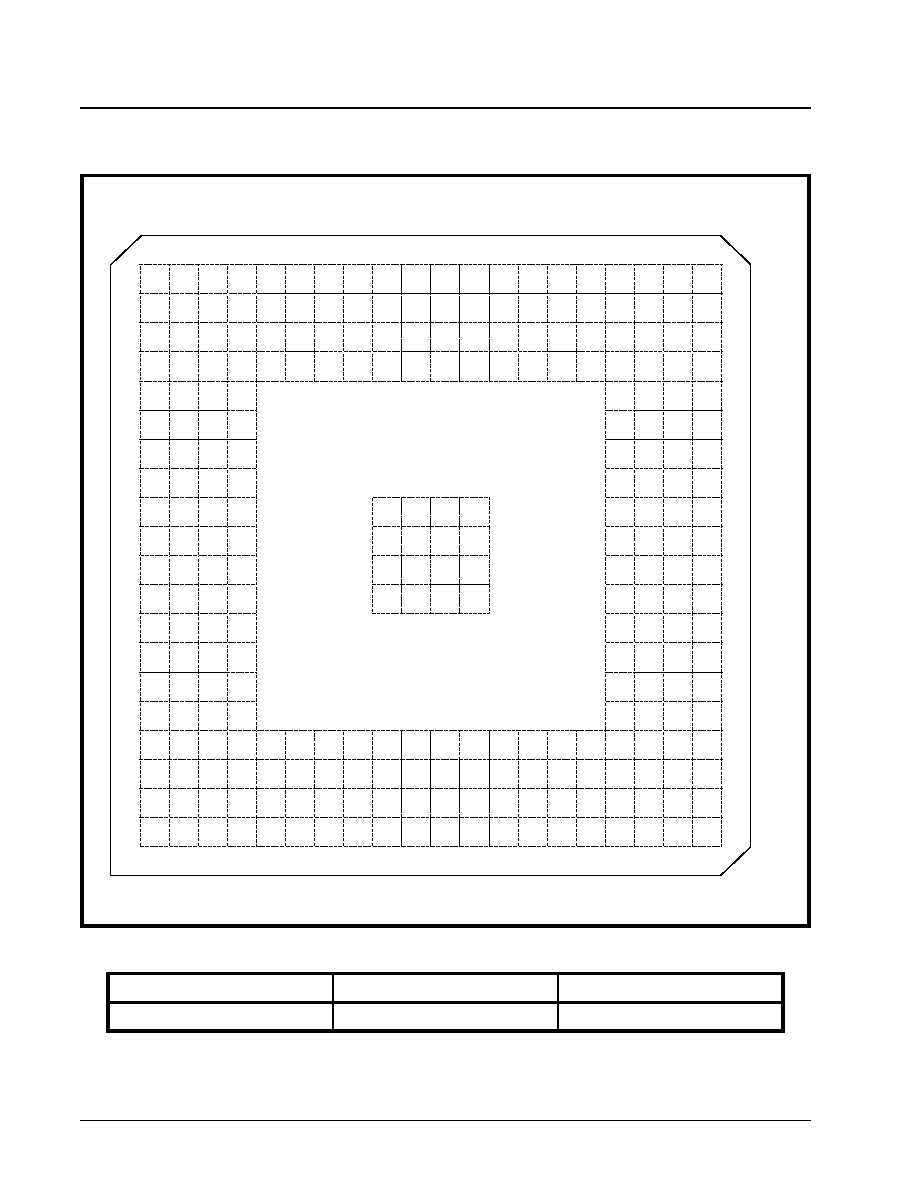
Figure 2. Pin Out ofthe XRT72L54 ......................................................................................................... 2
ORDERING INFORMATION ............................................................................................ 2
ELECTRICAL CHARACTERISTICS .............................................................................. 28
A
BSOLUTE
M
AXIMUMS
............................................................................................................................. 28
DC E
LECTRICAL
C
HARACTERISTICS
......................................................................................................... 28
AC E
LECTRICAL
C
HARACTERISTICS
......................................................................................................... 28
AC E
LECTRICAL
C
HARACTERISTICS
(C
ONT
.) ............................................................................................ 30
1.0 Timing Diagrams ................................................................................................................................. 34
Figure 3. Timing Diagram for Transmit Payload Input Interface, when the XRT72L54 Device is operating in
both the DS3 and Loop-Timing Modes ................................................................................................. 34
Figure 4. Timing Diagram for the Transmit Payload Input Interface, when the XRT72L54 Device is operating
in both the DS3 and Local-Timing Modes ............................................................................................. 34
Figure 5. Timing Diagram for the Transmit Payload Data Input Interface, when the XRT72L54 Device is
operating in both the DS3/Nibble and Looped-Timing Modes .............................................................. 35
Figure 6. Timing Diagram for the Transmit Payload Data Input Interface, when the XRT72L54 Device is
operating in the DS3/Nibble and Local-Timing Modes .......................................................................... 35
Figure 7. Timing Diagram for the Transmit Overhead Data Input Interface (Method 1 Access) .......... 36
Figure 8. Timing Diagram for the Transmit Overhead Data Input Interface (Method 2 Access) .......... 36
Figure 9. Transmit LIU Interface Timing - Framer is configured to update "TxPOS" and "TxNEG" on the
rising edge of "TxLineClk" ..................................................................................................................... 37
Figure 10. Transmit LIU Interface Timing - Framer is configured to update "TxPOS" and "TxNEG" on the
falling edge of "TxLineClk" .................................................................................................................... 37
Figure 11. Receive LIU Interface Timing - Framer is configured to sample "RxPOS" and "RxNEG" on the
rising edge of "RxLineClk" ..................................................................................................................... 38
Figure 12. Receiver LIU Interface Timing - Framer is configured to sample "RxPOS" and "RxNEG" on the
falling edge of "RxLineClk" .................................................................................................................... 38
Figure 13. Receive Payload Data Output Interface Timing .................................................................. 39
Figure 14. Receive Payload Data Output Interface Timing (Nibble Mode Operation) ......................... 39
Figure 15. Receive Overhead Data Output Interface Timing (Method 1 - Using RxOHClk) ................ 40
Figure 16. Receive Overhead Data Output Interface Timing (Method 2 - Using RxOHEnable) .......... 40
Figure 17. Microprocessor Interface Timing - Intel Type Programmed I/O Read Operations .............. 41
Figure 18. Microprocessor Interface Timing - Intel Type Programmed I/O Write Operations .............. 41
Figure 19. Microprocessor Interface Timing - Intel Type Read Burst Access Operation ..................... 42
Figure 20. Microprocessor Interface Timing - Intel type Write Burst Access Operation ....................... 42
Figure 21. Microprocessor Interface Timing - Motorola Type Programmed I/O Read Operation ........ 43
Figure 22. Microprocessor Interface Timing - Motorola Type Programmed I/O Write Operation ......... 43
Figure 23. Microprocessor Interface Timing - Reset Pulse Width ........................................................ 44
2.0 The Microprocessor Interface Block ................................................................................................. 45
2.1 C
HANNEL
S
ELECTION
WITHIN
THE
XRT72L54 D
EVICE
.......................................................................................... 45
T
ABLE
1: T
HE
R
ELATIONSHIP
BETWEEN
A
DDRESS
B
ITS
A9, A10
AND
THE
S
ELECTED
C
ONFIGURATION
R
EGISTER
B
ANK
...................................................................................................................................................... 45
Figure 24. Simple Block Diagram of the Microprocessor Interface Block, within the Framer IC .......... 46
2.2 T
HE
M
ICROPROCESSOR
I
NTERFACE
B
LOCK
S
IGNAL
.............................................................................................. 46
T
ABLE
2: D
ESCRIPTION
OF
THE
M
ICROPROCESSOR
I
NTERFACE
S
IGNALS
THAT
EXHIBIT
CONSTANT
ROLES
IN
BOTH
THE
I
NTEL
AND
M
OTOROLA
M
ODES
.......................................................................................................... 47
T
ABLE
3: P
IN
D
ESCRIPTION
OF
M
ICROPROCESSOR
I
NTERFACE
S
IGNALS
- W
HILE
THE
M
ICROPROCESSOR
I
NTER
-
FACE
IS
O
PERATING
IN
THE
I
NTEL
M
ODE
.................................................................................................. 47
T
ABLE
4: P
IN
D
ESCRIPTION
OF
THE
M
ICROPROCESSOR
I
NTERFACE
S
IGNALS
WHILE
THE
M
ICROPROCESSOR
I
N
-

XRT72L54
áç
áç
áç
áç
FOUR CHANNEL DS3/E3 FRAMER IC WITH HDLC CONTROLLER
REV. P1.1.2
PRELIMINARY
II
TERFACE
IS
OPERATING
IN
THE
M
OTOROLA
M
ODE
..................................................................................... 48
2.3 I
NTERFACING
THE
XRT72L54 DS3/E3 F
RAMER
TO
THE
L
OCAL
µC/µP
VIA
THE
M
ICROPROCESSOR
I
NTERFACE
B
LOCK
48
2.3.1 Interfacing the XRT72L54 DS3/E3 Framer to the Microprocessor over an 8 bit wide bi-directional Data Bus
48
2.3.2 Data Access Modes ................................................................................................................................ 49
Figure 25. Behavior of Microprocessor Interface signals during an Intel-type Programmed I/O Read Oper-
ation ....................................................................................................................................................... 50
Figure 26. Behavior of the Microprocessor Interface Signals, during an Intel-type Programmed I/O Write
Operation ............................................................................................................................................... 51
Figure 27. Illustration of the Behavior of Microprocessor Interface signals, during a Motorola-type Pro-
grammed I/O Read Operation ............................................................................................................... 52
Figure 28. Illustration of the Behavior of the Microprocessor Interface signal, during a Motorola-type Pro-
grammed I/O Write Operation ............................................................................................................... 53
Figure 29. Behavior of the Microprocessor Interface Signals, during the Initial Read Operation of a Burst
Cycle (Intel Type Processor) ................................................................................................................. 54
Figure 30. Behavior of the Microprocessor Interface Signals, during subsequent Read Operations within
the Burst I/O Cycle ................................................................................................................................ 55
Figure 31. Behavior of the Microprocessor Interface signals, during the Initial Write Operation of a Burst
Cycle (Intel-type Processor) .................................................................................................................. 57
Figure 32. Behavior of the Microprocessor Interface Signals, during subsequent Write Operations within
the Burst I/O Cycle ................................................................................................................................ 58
Figure 33. Behavior of the Microprocessor Interface Signals, during the Initial Read Operation of a Burst
Cycle (Motorola Type Processor) .......................................................................................................... 59
Figure 34. Behavior the Microprocessor Interface Signals, during subsequent Read Operations within the
Burst I/O Cycle (Motorola-type µC/µP) .................................................................................................. 60
Figure 35. Behavior of the Microprocessor Interface signals, during the Initial Write Operation of a Burst
Cycle (Motorola-type Processor) ........................................................................................................... 61
Figure 36. Behavior of the Microprocessor Interface Signals, during subsequent Write Operations with the
Burst I/O Cycle (Motorola-type µC/µP) .................................................................................................. 62
2.4 O
N
-C
HIP
R
EGISTER
O
RGANIZATION
...................................................................................................................... 62
2.4.1 Framer Register Addressing .................................................................................................................... 62
T
ABLE
5: R
EGISTER
A
DDRESSING
OF
THE
F
RAMER
P
ROGRAMMER
R
EGISTERS
......................................... 63
2.4.2 Framer Register Description .................................................................................................................... 66
P
ART
N
UMBER
R
EGISTER
(A
DDRESS
= 0
X
02) .......................................................................................... 69
V
ERSION
N
UMBER
R
EGISTER
(A
DDRESS
= 0
X
03) ..................................................................................... 69
B
LOCK
I
NTERRUPT
E
NABLE
R
EGISTER
(A
DDRESS
= 0
X
04) ........................................................................ 69
B
LOCK
I
NTERRUPT
S
TATUS
R
EGISTER
(A
DDRESS
= 0
X
05) ........................................................................ 70
TEST R
EGISTER
(A
DDRESS
= 0
X
0C) ....................................................................................................... 71
R
X
DS3 C
ONFIGURATION
& S
TATUS
R
EGISTER
(A
DDRESS
= 0
X
10) ........................................................... 72
R
X
DS3 S
TATUS
R
EGISTER
(A
DDRESS
= 0
X
11) ........................................................................................ 73
R
X
DS3 I
NTERRUPT
E
NABLE
R
EGISTER
(A
DDRESS
= 0
X
12) ....................................................................... 74
R
X
DS3 I
NTERRUPT
S
TATUS
R
EGISTER
(A
DDRESS
= 0
X
13) ....................................................................... 75
R
X
DS3 SYNC D
ETECT
E
NABLE
R
EGISTER
(A
DDRESS
= 0
X
14) ................................................................ 77
R
X
DS3 FEAC I
NTERRUPT
E
NABLE
/S
TATUS
R
EGISTER
(A
DDRESS
= 0
X
17) ............................................... 77
R
X
DS3 LAPD C
ONTROL
R
EGISTER
(A
DDRESS
= 0
X
18) ........................................................................... 78
R
X
DS3 LAPD S
TATUS
R
EGISTER
(A
DDRESS
= 0
X
19) .............................................................................. 79
2.4.3 Receive E3 Framer Configuration Registers (ITU-T G.832) .................................................................... 79
R
X
E3 C
ONFIGURATION
& S
TATUS
R
EGISTER
1 (A
DDRESS
= 0
X
10) ........................................................... 80
R
X
E3 C
ONFIGURATION
& S
TATUS
R
EGISTER
2 (A
DDRESS
= 0
X
11) ........................................................... 81
R
X
E3 I
NTERRUPT
E
NABLE
R
EGISTER
- 1 (A
DDRESS
= 0
X
12) .................................................................... 82
R
X
E3 I
NTERRUPT
E
NABLE
R
EGISTER
- 2 (A
DDRESS
= 0
X
13) .................................................................... 83
R
X
E3 I
NTERRUPT
S
TATUS
R
EGISTER
- 1 (A
DDRESS
= 0
X
14) .................................................................... 83
R
X
E3 I
NTERRUPT
S
TATUS
R
EGISTER
- 2 (A
DDRESS
= 0
X
15) .................................................................... 85
R
X
E3 LAPD C
ONTROL
R
EGISTER
(A
DDRESS
= 0
X
18) .............................................................................. 86

áç
áç
áç
áç
XRT72L54
FOUR CHANNEL DS3/E3 FRAMER IC WITH HDLC CONTROLLER
ADVANCED CONFIDENTIAL
REV. P1.1.2
III
R
X
E3 LAPD S
TATUS
R
EGISTER
(A
DDRESS
= 0
X
19) ................................................................................ 86
R
X
E3 NR B
YTE
R
EGISTER
(A
DDRESS
= 0
X
1A) ........................................................................................ 87
R
X
E3 GC B
YTE
R
EGISTER
(A
DDRESS
= 0
X
1B) ....................................................................................... 87
R
X
E3 TTB-0 R
EGISTER
(A
DDRESS
= 0
X
1C) ............................................................................................ 88
R
X
E3 TTB-1 R
EGISTER
(A
DDRESS
= 0
X
1D) ............................................................................................ 88
R
X
E3 TTB-2 R
EGISTER
(A
DDRESS
= 0
X
1E) ............................................................................................ 88
R
X
E3 TTB-3 R
EGISTER
(A
DDRESS
= 0
X
1F) ............................................................................................ 89
R
X
E3 TTB-4 R
EGISTER
(A
DDRESS
= 0
X
20) ............................................................................................ 89
R
X
E3 TTB-5 R
EGISTER
(A
DDRESS
= 0
X
21) ............................................................................................ 89
R
X
E3 TTB-6 R
EGISTER
(A
DDRESS
= 0
X
22) ............................................................................................ 89
R
X
E3 TTB-7 R
EGISTER
(A
DDRESS
= 0
X
23) ............................................................................................ 90
R
X
E3 TTB-8 R
EGISTER
(A
DDRESS
= 0
X
24) ............................................................................................ 90
R
X
E3 TTB-9 R
EGISTER
(A
DDRESS
= 0
X
25) ............................................................................................ 90
R
X
E3 TTB-10 R
EGISTER
(A
DDRESS
= 0
X
26) .......................................................................................... 91
R
X
E3 TTB-11 R
EGISTER
(A
DDRESS
= 0
X
27) .......................................................................................... 91
R
X
E3 TTB-12 R
EGISTER
(A
DDRESS
= 0
X
28) .......................................................................................... 91
R
X
E3 TTB-13 R
EGISTER
(A
DDRESS
= 0
X
29 ........................................................................................... 91
R
X
E3 TTB-14 R
EGISTER
(A
DDRESS
= 0
X
2A) .......................................................................................... 92
R
X
E3 TTB-15 R
EGISTER
(A
DDRESS
= 0
X
2B) .......................................................................................... 92
R
X
E3
SSM
R
EGISTER
(A
DDRESS
= 0
X
2B) ................................................................................................ 92
2.4.4 Receive E3 Framer Configuration Registers (ITU-T G.751) ................................................................... 93
R
X
E3 C
ONFIGURATION
& S
TATUS
R
EGISTER
- 1 G.751 (A
DDRESS
= 0
X
10) ............................................. 93
R
X
E3 C
ONFIGURATION
& S
TATUS
R
EGISTER
- 2 (A
DDRESS
= 0
X
11) ........................................................ 93
R
X
E3 I
NTERRUPT
E
NABLE
R
EGISTER
- 1 (A
DDRESS
= 0
X
12) ................................................................... 94
R
X
E3 I
NTERRUPT
E
NABLE
R
EGISTER
- 2 (A
DDRESS
= 0
X
13) ................................................................... 95
R
X
E3 I
NTERRUPT
S
TATUS
R
EGISTER
- 1 (A
DDRESS
= 0
X
14) ................................................................... 95
R
X
E3 I
NTERRUPT
S
TATUS
R
EGISTER
- 2 (A
DDRESS
= 0
X
15) ................................................................... 96
R
X
E3 LAPD C
ONTROL
R
EGISTER
(A
DDRESS
= 0
X
18) ............................................................................. 97
R
X
E3 LAPD S
TATUS
R
EGISTER
(A
DDRESS
= 0
X
19) ................................................................................ 97
R
X
E3 S
ERVICE
B
IT
R
EGISTER
(A
DDRESS
= 0
X
1A) ................................................................................... 98
2.4.5 Transmit DS3 Configuration Registers .................................................................................................... 98
T
RANSMIT
DS3 C
ONFIGURATION
R
EGISTER
(A
DDRESS
= 0
X
30) ............................................................... 99
T
RANSMIT
DS3 FEAC C
ONFIGURATION
& S
TATUS
R
EGISTER
(A
DDRESS
= 0
X
31) .................................. 100
T
X
DS3 FEAC R
EGIS
T
ER
(A
DDRESS
= 0
X
32) ........................................................................................ 101
T
X
DS3 LAPD C
ONFIGURATION
R
EGISTER
(A
DDRESS
= 0
X
33) ............................................................... 101
T
X
DS3 LAPD S
TATUS
AND
I
NTERRUPT
R
EGISTER
(A
DDRESS
= 0
X
34) ................................................... 102
T
X
DS3 M-B
IT
M
ASK
R
EGISTER
(A
DDRESS
= 0
X
35) ............................................................................... 102
T
X
DS3 F-B
IT
M
ASK
R
EGISTER
- 1 (A
DDRESS
= 0
X
36) ........................................................................... 103
T
X
DS3 F-B
IT
M
ASK
R
EGISTER
- 2 (A
DDRESS
= 0
X
37) ........................................................................... 104
T
X
DS3 F-B
IT
M
ASK
R
EGISTER
- 3 (A
DDRESS
= 0
X
38) ........................................................................... 104
T
X
DS3 F-B
IT
M
ASK
R
EGISTER
- 4 (A
DDRESS
= 0
X
39) ........................................................................... 104
2.4.6 Transmit E3 (ITU-T G.832) Configuration Registers ............................................................................. 104
T
X
E3 C
ONFIGURATION
R
EGISTER
(A
DDRESS
= 0
X
30) ............................................................................ 105
T
X
E3 LAPD C
ONFIGURATION
R
EGISTER
(A
DDRESS
= 0
X
33) ................................................................. 106
T
X
E3 LAPD S
TATUS
AND
I
NTERRUPT
R
EGISTER
(A
DDRESS
= 0
X
34) ...................................................... 106
T
X
E3 GC B
YTE
R
EGISTER
(A
DDRESS
= 0
X
35) ...................................................................................... 107
T
X
E3 MA B
YTE
R
EGISTER
(A
DDRESS
= 0
X
36) ...................................................................................... 108
T
X
E3 MA B
YTE
R
EGISTER
(A
DDRESS
= 0
X
36) ...................................................................................... 108
T
X
E3 NR B
YTE
R
EGISTER
(A
DDRESS
= 0
X
37) ...................................................................................... 108
T
X
E3 TTB-0 R
EGISTER
(A
DDRESS
= 0
X
38) ........................................................................................... 109
T
X
E3 TTB-1 R
EGISTER
(A
DDRESS
= 0
X
39) ........................................................................................... 109
T
X
E3 TTB-2 R
EGISTER
(A
DDRESS
= 0
X
3A) .......................................................................................... 109
T
X
E3 TTB-3 R
EGISTER
(A
DDRESS
= 0
X
3B) .......................................................................................... 110
T
X
E3 TTB-4 R
EGISTER
(A
DDRESS
= 0
X
3C) .......................................................................................... 110
T
X
E3 TTB-5 R
EGISTER
(A
DDRESS
= 0
X
3D) .......................................................................................... 111