/home/web/doc/html/exar/208056
Exar
Corporation 48720 Kato Road, Fremont CA, 94538
·
(510) 668-7000
·
FAX (510) 668-7017
·
www.exar.com
áç
áç
áç
áç
PRELIMINARY
XRT72L71
DS3 ATM UNI/CLEAR CHANNEL FRAMER
DECEMBER 2000
REV. P1.0.5
GENERAL DESCRIPTION
The XRT72L71 DS3 ATM User Network Interface
(UNI)/Clear-Channel Framer is designed to function
as either a DS3 ATM UNI or Clear channel framer.
For ATM UNI applications, this device provides the
ATM Physical Layer (Physical Medium Dependent
and Transmission Convergence sub-layers) interface
for both the public and private networks at DS3 rates.
For Clear-Channel framer applications, this device
supports the transmission and reception of "user da-
ta" via the DS3 payload bits.
The XRT72L71incorporates Receive, Transmit, Micro-
processor Interface, Performance Monitor, Test and Di-
agnostic and Line Interface Unit Scan Drive sections.
APPLICATIONS
· Private User Network Interfaces
· ATM Switches
· ATM Concentrators
· DSLAM Equipment
· DS3 Frame Relay Equipment
FEATURES
· Compliant with UTOPIA Level 1 and 2 with 8 or 16
Bit Interface Specification and supports UTOPIA
Bus speeds of up to 50 MHz
· Contains on-chip 16 cell FIFO in both the Transmit
(TxFIFO) and Receive Directions (RxFIFO)
· Contains on-chip 54 byte Transmit OAM Cell buffer
and a 108 byte Receive OAM cell buffer, for trans-
mission, reception and processing of OAM cells.
· Supports PLCP or ATM Direct Mapping modes
· Supports M13 and C-Bit Parity Framing Formats
· Supports DS3 Clear Channel Framing Applications
· Includes PRBS Generator and Receiver
· Supports Local, Remote-Line, Cell, and PLCP
Loop-backs
· Interfaces to 8 or 16 Bit wide Motorola and Intel µPs
· Low power 3.3V, 5V input tolerant, CMOS
· 160 pin PQFP Package
· 3 and 4 Channel Version also Available
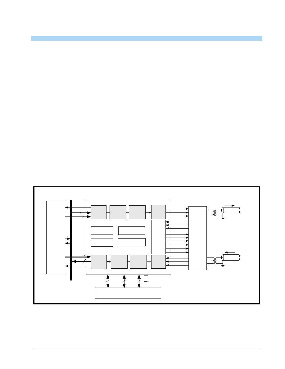
F
IGURE
1. XRT72L71 S
IMPLIFIED
B
LOCK
D
IAGRAM
WITH
S
YSTEM
I
NTERFACES
XRT73L00
RxUClav
DS3/E3 LIU
Tx
Rx
TPDATA
TNDATA
TCK
DMO
RLOS
RLOL
LLB
RLB
TAOS
TxLEV
ENCODIS
ReQDIS
RPOS
RNEG
RCLK1
UTOPIA BUS
Level 1 or 2
DS3
44.736 MHz
16
16
25, 33 or 50 MHz
Intel/Motorola
µ
µ
µ
µ
P
Configuration, Control and Status Monitor
ATM Switch
D[15:0]
D[7:0]
A[8:0]
4
TxUClav
5
Address
5
XRT72L71
Address
ATM
Layer
Processor
Tx
UTOPIA
Interface
Tx
Cell
Processor
Tx
PLCP
Processor
Tx
DS3
Framer
Performance
Monitor
Microprocessor
Interface
FEAC
Processor
LAPD
Transceiver
Rx
UTOPIA
Interface
Rx
DS3
Framer
Rx
PLCP
Processor
Rx
Cell
Processor
LIU
Interface
Drive
and
Scan
75
coax
75
coax
TxPOS
TxNEG
TCK
DMO
RLOS
RLOL
LLOOP
RLOOP
TAOS
TxLEV
Req
RxPOS
RxNEG
RxLineClk
EncoDis
WR_RW
ALE_AS
RD_DS
RDY_DTCK
XRT72L71
áç
áç
áç
áç
DS3 ATM UNI/CLEAR CHANNEL FRAMER
REV. P1.0.5
PRELIMINARY
2
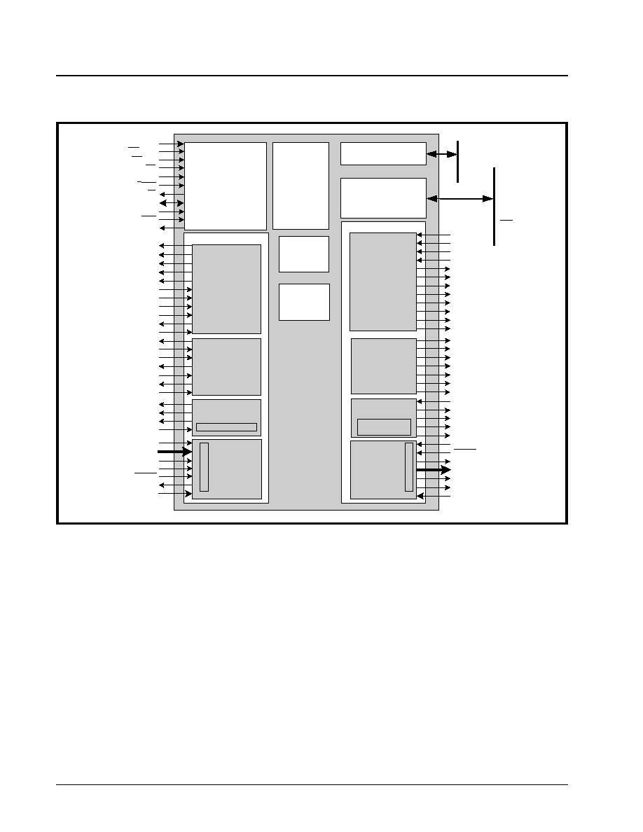
F
IGURE
2. B
LOCK
D
IAGRAM
OF
THE
XRT72L71 DS3 UNI
Test and Diagnostic
Line Interface
Drive and Scan
Performance
Monitor
Receive
DS3
Framer
Receive Cell
Processor
Receive
UTOPIA
Interface
Transmitter
Receiver
LAPD
Transceiver
Microprocessor
Interface
(Programmable
Registers and
Interrupt Block)
FEAC
Processor
Transmit
UTOPIA
Interface
TxUClk
TxUData[15:0]
TxUPrty
TxUSoC
TxUEn
TxUClav
TxUAddr[4:0]
Transmit PLCP
Processor/
Clear Channel
Transmit Serial Data
Processor
Transmit
DS3
Framer
Receive PLCP
Processor/
Clear Channel
Receive Serial Data
Processor
16 cell FIFO
16 cell FIFO
2x54b OAM
Buffer
Transmit Cell
Processor
54b OAM Buffer
A[8:0]
WR_RW
RD_DS
CS
ALE_AS
Reset
Int
D[15:0]
Width16
MOTO/Intel
RDY_DTCK
TxPOS
TxNEG
TxFrame
TxOHClk
TxLineClk
TxAISEn
TxFrameRef
TxInClk
TxOHIns
TxOHFrame
TxOH
TxPOHFrame
8KRef
StuffCtl
TxOHInd/TxPFrame
TxSerData/TxPOH
TxPOHClk
TxPOHIns
TxCellTxed
TxGFCClk
TxGFCMSB
TxGFC
TDO
TDI
TestMode
TCK
TMS
TAOS
DMO
RLOL
TxLev
RLOOP
LLOOP
Req
RxRed
EncoDis
RxLineClk
RxNEG
RxPOS
RLOS
RxAIS
RxOHClk
RxOH
RxSerClk
RxLOS
RxFrame
RxOHFrame
RxOOF
RxPRed
RxPOHFrame
RxSerClk/RxPOHClk
RxSerData/RxPOH
RxOHInd/RxPFrame
RxPLOF
RxPOOF
RxLCD
RxCellRxed
RxGFCClk
RxGFCMSB
RxGFC
RxUClk
RxUEn
RxUPrty
RxUData[15:0]
RxUSoC
RxUClav
RxUAddr[4:0]

áç
áç
áç
áç
XRT72L71
DS3 ATM UNI/CLEAR CHANNEL FRAMER
PRELIMINARY
REV. P1.0.5
3
SYSTEM/FUNCTIONAL DESCRIPTION
FUNCTIONAL DESCRIPTION
The XRT72L71 DS3 ATM UNI/Framer IC can be con-
figured to operate in either the "ATM UNI" or in the
"Clear-Channel-Framer" Mode.
A brief listing of the features and description for each
of these operating modes is presented below.
THE ATM UNI MODE OF OPERATION
When the XRT72L71 UNI/Framer has been config-
ured to operate in the "ATM UNI" Mode, it can func-
tionally be subdivided into 6 different sections, as
shown in Figure 2.
· Receive Section
· Transmit Section
· Microprocessor Interface Section
· Performance Monitor Section
· Test and Diagnostic Section
· Line Interface Unit Scan Drive Section
The features of each of these functional sections are
briefly outlined below.
THE RECEIVE SECTION
The purpose of the Receive Section of the XRT72L71
DS3 ATM UNI is to allow a local ATM Layer (or ATM
Adaptation Layer) processor to receive ATM cell data
from a remote piece of equipment via a public or
leased DS3 transport medium.
The Receive Section of the XRT72L71 DS3 UNI con-
sists of the following functional blocks.
· Receive DS3 Framer Block
· Receive PLCP (Physical Layer Convergence Proto-
col) Processor Block
· Receive Cell Processor Block
· Receive UTOPIA Interface Block
Each of these functional blocks, within the Receive
Section of the UNI Framer will do the following:
The Rx DS3 Framer Block
· Capable of receiving data, from the LIU IC, in either
the "Single-Rail" or "Dual-Rail" mode.
· Capable of "sampling" the "inbound" DS3 data (at
the "RxPOS" and "RxNEG" input pins) upon either
the rising or falling edge of the "RxLineClk" signal.
· The Receive DS3 Framer will synchronize to the
incoming DS3 data stream and remove or process
the DS3 Framing/Overhead Bits. This procedure
will result in either extracting PLCP frame data or
"Direct-Mapped" ATM Cell data, from the payload
portion of the incoming DS3 data stream.
· The Receive DS3 Framer can be used to receive
FEAC (Far End Alarm & Control) messages via an
on-chip FEAC Transceiver.
· The Receive DS3 Framer includes an on-chip
LAPD Receiver along with 88 bytes of on-chip RAM
that can receive incoming path maintenance data
link messages from the Remote Terminal Equip-
ment.
· Detects and generates interrupts upon "Detection
of P and CP-bit Errors", "Change of State in LOS,
AIS, OOF and FERF", "Receipt of New LAPD
(PMDL) Message", "Validation and Removal of
FEAC Message".
N
OTE
: The Receive DS3 Framer supports both M13 and C-
bit Parity Frame Formats.
The Rx PLCP Processor Block
· The Receive PLCP Processor will identify the frame
boundary of each incoming PLCP frame, extract
and process the overhead bytes of these PLCP
frames (applies only if the UNI is operating in the
PLCP Mode). The Receive PLCP Processor will
also perform some error checking on the incoming
PLCP frames. The Receive PLCP Processor will
inform the Remote Terminal Equipment of the
results of this error-checking by internally routing
these results to the "Near-End" Transmit PLCP Pro-
cessor, for transmission back out to the RemoteTer-
minal Equipment.
The Rx Cell Processor Block
· The Receive Cell Processor will perform the follow-
ing functions:
Cell Delineation
HEC Byte Verification of incoming cells
(optional)
Cell-payload de-scrambling (optional)
Idle cell detection and removal (optional)
User and OAM Cell Filtering (optional)
OAM Cell Processing (optional)
· The UNI provides 108 bytes of on-chip RAM that
allows for the reception and processing of selected
OAM cells.
· The Receive Cell Processor block will also verify
the CRC-10 value within all received OAM cells, per
ITU-T I.610.

XRT72L71
áç
áç
áç
áç
DS3 ATM UNI/CLEAR CHANNEL FRAMER
REV. P1.0.5
PRELIMINARY
4
· Detects and generates interrupts upon "Detection
of HEC Byte errors", "Change in LCD (Loss of Cell
Delineation) condition" and "Receipt of OAM Cell".
The Receive UTOPIA Interface Block
· Provides a "UTOPIA Level -2" compliant interface to
either the ATM or the ATM Adaptation Layer.
· Can be configured to operate in either the "Single-
PHY" or "Multi-PHY" Modes.
· Supports either "Cell-Level" or "Octet-Level" Hand-
shaking.
· Receive UTOPIA Data Bus can be configured to be
either 8 or 16-bits wide.
· The RxFIFO, within the Receive UTOPIA Interface
block will temporarily hold any ATM cells that pass
through the Receive Cell Processor, where they can
be read out by the ATM Layer processor, over the
Receive UTOPIA Data Bus.
· The size of the "RxFIFO" is 16 cells.
· Supports read operations (from the ATM Layer
device) at rates upto 50MHz.
· Detects and generates interrupts upon "Detection
of RUNT cells" and "Overrun of RxFIFO".
THE TRANSMIT SECTION
The purpose of the Transmit section of the XRT72L71
DS3 ATM UNI is to allow a local ATM Layer (or ATM
Adaptation Layer) processor to transmit ATM Cell da-
ta to a remote piece of equipment via a public or
leased DS3 transport medium.
The Transmit Section of the XRT72L71 DS3 UNI con-
sists of the following functional blocks.
· Transmit UTOPIA Interface Block
· Transmit Cell Processor Block
· Transmit PLCP Processor Block
· Transmit DS3 Framer Block
Each of these functional blocks, within the Transmit
Section (of the UNI/Framer) will do the following:
Transmit UTOPIA Interface Block
· Can be configured to operate in either the "Single-
PHY" or Multi-PHY" Mode.
· Supports either the "Cell-Level" or "Octet-Level"
Handshaking Mode.
· Transmit UTOPIA Data Bus can be configured to be
either 8 or 16-bits wide.
· Allow the ATM Layer processor to write ATM cells
into the Transmit FIFO (within the Transmit UTOPIA
Interface block) via a standard UTOPIA Level 2
interface.
· The size of the "TxFIFO" is 16 cells. However, the
operating depth can be configured to be 4, 8, 12 or
16 cells.
· Supports write operations (from the ATM Layer
device) at rates upto 50MHz.
· Detects and generates interrupts upon "Detection
of Parity Errors", "Detection of RUNT cells" and
"Overrun of TxFIFO".
Transmit Cell Processor Block
· The Transmit Cell Processor will read in ATM cells
from the Transmit FIFO (if available) for further
processing.
· If no cell is available within the Transmit FIFO, then
the Transmit Cell Processor will automatically gen-
erate an Idle cell. The UNI is equipped with on-chip
registers to allow for the generation of customized
Idle cells.
· The UNI provides 54 bytes of on-chip RAM that
allows for the generation and transmission of "user-
specified" OAM cells. The Transmit Cell Processor
will generate and transmit these OAM cells upon
software command.
· The Transmit Cell Processor block will also com-
pute and insert a CRC-10 value into each "out-
bound" OAM cell, per ITU-T I.610.
· The Transmit Cell Processor will (optionally) scramble
the Cell Payload bytes and (optionally) compute
and insert the HEC (Header Error Check) byte. This
HEC byte will be inserted into the fifth octet of each
cell prior to being transferred to the Transmit PLCP
Processor (or the Transmit DS3 Framer).
Transmit PLCP Processor Block
· The Transmit PLCP Processor will pack 12 ATM cells
into each PLCP frame and automatically determine
the nibble-stuffing option of the current PLCP frame.
These PLCP frames will also include an overhead
byte that reflect BIP-8 (Bit Interleaved Parity) calcula-
tion results, a byte that reflects the current stuffing
option status of the current PLCP frame, Path Over-
head and Identifier bytes, and diagnostic-related
bytes reflecting any detected BIP-8 errors and
alarm conditions detected in the Receive section of
the UNI chip.
Transmit DS3 Framer Block
· These PLCP frames (or "Direct Mapped" ATM cells)
will be inserted into the payload of an outgoing DS3
frame, for transmission to the "Remote" Terminal, by
the Transmit DS3 Framer.
· The Transmit DS3 Framer will transmit FEAC (Far
End Alarm & Control) messages to the Remote Ter-
minal Equipment via an on-chip FEAC Transceiver.

áç
áç
áç
áç
XRT72L71
DS3 ATM UNI/CLEAR CHANNEL FRAMER
PRELIMINARY
REV. P1.0.5
5
· Additionally, the Transmit DS3 Framer can transmit
path maintenance data link messages to the
Remote Terminal Equipment via the on-chip LAPD
Transmitter.
· Generates interrupts upon "Completion of Trans-
mission of LAPD and FEAC" Messages.
Note: The Transmit DS3 Framer will support either M13 or
C-bit Parity Framing Formats.
CLEAR-CHANNEL-FRAMING MODE OF OPERA-
TION
When the XRT72L71has been configured to operate
in the "Clear-Channel Framer" mode, it can be func-
tionally subdivided into 6 different sections.
· Receive Section
· Transmit Section
· Microprocessor Interface Section
· Performance Monitor Section
· Test and Diagnostic Section
· Line Interface Unit Scan/Drive Section.
The features of each of the "Receive" and "Transmit"
Section (for Clear-Channel Framer applications) are
listed below.
THE RECEIVE SECTION
The purpose of the Receive Section of the XRT72L71
Clear-Channel DS3 Framer is to allow a given Termi-
nal to receive data from a remote terminal, which is
being transported over a DS3 data stream.
The Receive Section of the XRT72L71 Clear-Channel
DS3 Framer IC consists of the following functional
blocks.
· Receive DS3 Framer block
· Receive Overhead Data Output Interface block
· Receive Payload Data Output Interface block
It should be noted that the "Receive DS3 Framer"
block is also active, when the XRT72L71 has been
configured to operate in the "ATM UNI" Mode.
Each of these functional blocks, within the Receive
Section of the Framer will do the following.
· The Receive DS3 Framer block will synchronize to
the incoming DS3 data stream. All "inbound" DS3
data will be routed to the "Receive Payload Data
Output Interface" block. All overhead bits (which
are extracted from each "inbound" DS3 frame) will
be routed to the "Receive Overhead Data Output
Interface" block.
· The Receive DS3 Framer block can also be used to
receive FEAC (Far-End-Alarm & Control) mes-
sages and PMDL (Path Maintenance Data Link)
messages via the "on-chip" Receive HDLC Control-
ler block.
· The Receive Overhead Output Interface block out-
puts all overhead bits, which have been received
via the "inbound" DS3 data stream. The purpose of
the "Receive Overhead Output Interface" block is to
permit external circuitry (within the local terminal
equipment) to have access to these overhead bits,
for additional processing.
· The Receive Payload Data Output Interface block
outputs all data bits which have been received via
the XRT72L71, to the local terminal equipment.
Since the "Receive Payload Data Output Interface"
block outputs both "payload" and "overhead" data
bits, to the local terminal equipment; the "Receive
Payload Data Output Interface" block also includes
an "Overhead Indicator" output pin. This output pin
pulses "High" whenever an overhead bit is being
output via the "Receive Payload Data Output Inter-
face" block.
THE TRANSMIT SECTION
The purpose of the Transmit Section of the
XRT72L71 Clear-Channel DS3 Framer is to allow a
local terminal to transmit data to a remote terminal
equipment, via a DS3 transport medium.
The Transmit Section of the XRT72L71 Clear-Chan-
nel DS3 Framer consists of the following functional
blocks.
· Transmit Payload Data Input Interface block
· Transmit Overhead Data Input Interface block
· Transmit DS3 Framer block
It should be noted that the "Transmit DS3 Framer"
block is also active, whenever the XRT72L71 has
been configured to operate in the "ATM UNI" Mode.
The Transmit Section of the Clear-Channel DS3
Framer will:
· Accept all "user" data, (which is required to be
transported to the Remote Terminal Equipment via
a DS3 data stream) via the "Transmit Payload Data
Input Interface block.
· Optionally accepts and insert overhead bits (into
the "outbound" DS3 data-stream) via the "Transmit
Overhead Input Interface block.
· The Transmit DS3 Framer block will accept payload
data (from the Transmit Payload Data Input Inter-
face block) and overhead data (from the Transmit
Overhead Data Input Interface block) and will cre-
ate a DS3 data stream. If no overhead data is
inserted via the "Transmit Overhead Data Input
interface" block, then the "Transmit DS3 Framer"
block will insert its own values for the overhead bits.
Document Outline