 | –≠–ª–µ–∫—Ç—Ä–æ–Ω–Ω—ã–π –∫–æ–º–ø–æ–Ω–µ–Ω—Ç: XRT7302 | –°–∫–∞—á–∞—Ç—å:  PDF PDF  ZIP ZIP |

Exar
Corporation 48720 Kato Road, Fremont CA, 94538
∑
(510) 668-7000
∑
FAX (510) 668-7017
∑
www.exar.com
·Á
·Á
·Á
·Á
XRT7302
2 CHANNEL E3/DS3/STS-1 LINE INTERFACE UNIT
SEPTEMBER 2000
REV. 1.1.6
GENERAL DESCRIPTION
The XRT7302 Dual Channel E3/DS3/STS-1 Trans-
ceiver IC consists of two fully integrated transmitter
and receiver line transceivers designed for E3, DS3
or SONET STS-1 applications.
Each channel can be configured to support the E3
(34.368 Mbps), DS3 (44.736 Mbps) or the SONET
STS-1 (51.84 Mbps) rates. Each channel can be con-
figured to operate in a mode/data rate that is indepen-
dent of the other channel.
In the transmit direction, each channel in the
XRT7302 encodes input data to either B3ZS or HDB3
format and converts the data into the appropriate
pulse shapes for transmission over coaxial cable via a
1:1 transformer.
In the receive direction, the XRT7302 can perform
Equalization on incoming signals, perform Clock Re-
covery, decode data from either B3ZS or HDB3 for-
mat, convert the receive data into TTL/CMOS format,
check for LOS or LOL conditions and detect and de-
clare the occurrence of Line Code Violations.
FEATURES
∑ Meets E3/DS3/STS-1 Jitter Tolerance Require-
ments
∑ Contains a 4-Wire Microprocessor Serial Interface
∑ Full Loop-back Capability
∑ Transmit and Receive Power Down Modes
∑ Full Redundancy Support
∑ Single +5V Power Supply
∑ Uses Minimum External components
∑ Operates over -40∞C to +85∞C Temperature Range
∑ Available in an 80 pin TQFP Thermal Enhanced
package with integral Heat Sink
APPLICATIONS
∑ Digital Cross Connect Systems
∑ CSU/DSU Equipment
∑ Routers
∑ Fiber Optic Terminals
∑ Multiplexers
∑ ATM Switches
XRT7302 BLOCK DIAGRAM
AGC/
Equalizer
Serial
Processor
Interface
Peak Detector
LOS Detector
Pulse
Shaping
HDB3/
B3ZS
Encoder
Transmit
Logic
Duty Cycle Adjust
Slicer
Clock
Recovery
Data
Recovery
Invert
Loop MUX
HDB3/
B3ZS
Decoder
SDI
SDO
SClk
CS
REGR
TTIP(n)
TRing(n)
RTIP(n)
RRing(n)
REQEN(n)
RxClk(n)
RPOS(n)
RNEG(n)
LCV(n)
RLOS(n)
LLB(n)
RLB(n)
TAOS(n)
TPData(n)
TNData(n)
TxClk(n)
E3_Ch(n) STS-1/DS3_Ch(n) Host/HW RLOL(n) ExClk(n) RxClkINV
Channel 0
Channel 1
Device
Monitor
Tx
Control
TxLEV(n)
TxOFF(n)
DMO(n)
MTIP(n)
MRing(n)
ENDECDIS
Notes: 1. (n) = 0 or 1 for the respective channel.
2. Serial Processor Interface pins are shared by both Channels in HOST Mode and are redefined in Hardware Mode.
LOSTHR(n)
RxOFF(n)

XRT7302
2 CHANNEL E3/DS3/STS-1 LINE INTERFACE UNIT
·Á
·Á
·Á
·Á
REV. 1.1.6
2
TRANSMIT INTERFACE CHARACTERISTICS
∑ Accepts either Single-Rail or Dual-Rail data from
Terminal Equipment and generates a bipolar signal
∑ Integrated Pulse Shaping Circuit
∑ Built-in B3ZS/HDB3 Encoder (which can be dis-
abled)
∑ Contains Transmit Clock Duty Cycle Correction Cir-
cuit on-chip
∑ Generates pulses that comply with the ITU-T G.703
pulse template (E3 applications)
∑ Generates pulses that comply with the DSX-3 pulse
template, as specified in Bellcore GR-499
-CORE
and ANSI T1.102_1993
∑ Generates pulses that comply with the STSX-1
pulse template, as specified in Bellcore GR-253-
CORE
∑ Transmitter can be turned off in order to support
redundancy designs
RECEIVE INTERFACE CHARACTERISTICS
∑ Integrated Adaptive Receive Equalization
(Optional) and Timing Recovery
∑ Declares and Clears the LOS alarm per ITU-T
G.775 requirements for E3 and DS3 applications
∑ Meets Jitter Tolerance Requirements, as specified
in ITU-T G.823_1993 for E3 Applications
∑ Meets Jitter Tolerance Requirements, as specified
in Bellcore GR-499-CORE for DS3 Applications
∑ Declares Loss of Signal (LOS) and Loss of Lock
(LOL) Alarms
∑ Built-in B3ZS/HDB3 Decoder (which can be dis-
abled)
∑ Recovered Data can be automatically muted while
the LOS Condition is declared
∑ Outputs either Single-Rail or Dual-Rail data to the
Terminal Equipment
∑ Receiver can be powered down in order to con-
serve power in redundancy designs
PIN OUT OF THE XRT7302
TxLEV0
TAOS0
DVDD
DMO0
DGND
AGND
DVDD
Host/(HW)
RxClk0
RNEG0
RPOS0
DGND
RLOS0
LCV0
RLOL0
EXClk0
CS/(ENDECDIS)
SClk/(RxOff1)
SDI/(RxOff0)
SDO/(E3_Ch0)
STS-1/DS3_Ch0
ICT
LOSTHR0
LLB0
RLB0
AVDD
RRing0
RTIP0
AGND
REQEN0
REQEN1
AGND
RTIP1
RRing1
AVDD
RLB1
LLB1
LOSTHR1
E3_Ch1
SR/DR
TxLEV1
TAOS1
DVDD
DMO1
DGND
AGND
DVDD
LOSMUTEN
RxClk1
RNEG1
RPOS1
DGND
RLOS1
LCV1
RLOL1
EXClk1
VDD
GND
REGR/(RxClkINV)
STS-1/DS3_Ch1
80 Lead TQFP
1
2
3
4
5
6
7
8
9
10
11
12
13
14
15
16
17
18
19
20
60
59
58
57
56
55
54
53
52
51
50
49
48
47
46
45
44
43
42
41
21
22
23
24
25
26
27
28
29
30
31
32
33
34
35
36
37
38
39
40
80
79
78
77
76
75
74
73
72
71
70
69
68
67
66
65
64
63
62
61
TxOff0
TxClk0
TPDATA0
TNDATA0
MTIP0
MRing0
AVDD
TTIP0
TRing0
AGND
AGND
TRing1
TTIP1
AVDD
MRing1
MTIP1
TNDATA1
TPDATA1
TxClk1
TxOff1

·Á
·Á
·Á
·Á
2 CHANNEL E3/DS3/STS-1 LINE INTERFACE UNIT
XRT7302
REV. 1.1.6
I
TABLE OF CONTENTS
General description ........................................................................................................... 1
FEATURES ................................................................................................................................................ 1
APPLICATIONS ......................................................................................................................................... 1
XRT7302 BLOCK DIAGRAM ..................................................................................................................... 1
TRANSMIT INTERFACE CHARACTERISTICS ........................................................................................ 2
RECEIVE INTERFACE CHARACTERISTICS ........................................................................................... 2
PIN OUT OF THE XRT7302 ...................................................................................................................... 2
................................................................................. TABLE OF CONTENTS I
Pin descriptions ................................................................................................................. 3
ELECTRICAL CHARACTERISTICS ................................................................................. 14
ABSOLUTE MAXIMUM RATINGS ................................................................................................... 14
Figure 1.Transmit Pulse Amplitude Test Circuit for E3, DS3 and STS-1 Rates (typical channel shown) ...... 16
Figure 2.Timing Diagram of the Transmit Terminal Input Interface ................................................................ 16
Figure 3.Timing Diagram of the Receive Terminal Output Interface .............................................................. 16
Figure 4.Microprocessor Serial Interface Data Structure ............................................................................... 20
Figure 5.Timing Diagram for the Microprocessor Serial Interface .................................................................. 21
SYSTEM DESCRIPTION ................................................................................................... 22
THE TRANSMIT SECTION - CHANNELS 0 AND 1 ................................................................................ 22
THE RECEIVE SECTION - CHANNELS 0 AND 1 ................................................................................... 22
THE MICROPROCESSOR SERIAL INTERFACE ................................................................................... 22
Table 1:Role of Microprocessor Serial Interface pins when the XRT7302 is operating in the Hardware Mode ..
22
Figure 6.Functional Block Diagram of the XRT7302 ...................................................................................... 23
1.0 SELECTING THE DATA RATE ......................................................................................................... 23
1.1 C
ONFIGURING
C
HANNEL
(
N
) ............................................................................................................ 23
Table 2:Addresses and Bit Formats of XRT7302 Command Registers ......................................................... 24
Table 3:Selecting the Data Rate for Channel(n) of the XRT7302, via the E3_Ch(n) and STS-1/DS3_Ch(n) input
pins (Hardware Mode) ....................................................................................................................... 24
COMMAND REGISTER CR4-(N) .................................................................................................... 25
Table 4:Selecting the Data Rate for Channel(n) of the XRT7302 via the STS-1/DS3_Ch(n) and the E3_Ch(n)
bit-fields in the Appropriate Command Register (HOST Mode) ........................................................ 25
2.0 THE TRANSMIT SECTION ............................................................................................................... 25
2.1 T
HE
T
RANSMIT
L
OGIC
B
LOCK
......................................................................................................... 25
Accepting Dual-Rail Data from the Terminal Equipment ................................................................... 25
Figure 7. The typical interface for Data Transmission in Dual-Rail Format from the Transmitting Terminal Equip-
ment to the Transmit Section of a channel of the XRT7302 ............................................................. 26
Figure 8.How the XRT7302 Samples the data on the TPData and TNData input pins .................................. 26
Configure Channel(n) to accept Single-Rail Data from the Terminal Equipment .............................. 26
COMMAND REGISTER CR1-(N) ..................................................................................................... 26
Figure 9.The Behavior of the TPData and TxClk Input Signals while the Transmit Logic Block is Accepting Sin-
gle-Rail Data from the Terminal Equipment ..................................................................................... 27
2.2 T
HE
T
RANSMIT
C
LOCK
D
UTY
C
YCLE
A
DJUST
C
IRCUITRY
................................................................. 27
2.3 T
HE
HDB3/B3ZS E
NCODER
B
LOCK
............................................................................................... 27
B3ZS Encoding .................................................................................................................................. 27

XRT7302
2 CHANNEL E3/DS3/STS-1 LINE INTERFACE UNIT
·Á
·Á
·Á
·Á
REV. 1.1.6
II
Figure 10.An Example of B3ZS Encoding ...................................................................................................... 28
HDB3 Encoding .................................................................................................................................. 28
Figure 11.An Example of HDB3 Encoding ...................................................................................................... 28
Disabling the HDB3/B3ZS Encoder ................................................................................................... 28
COMMAND REGISTER CR2-(N) ..................................................................................................... 29
2.4 T
HE
T
RANSMIT
P
ULSE
S
HAPING
C
IRCUITRY
.................................................................................... 29
Figure 12.The Bellcore GR-499-CORE Transmit Output Pulse Template for DS3 Applications .................... 29
Figure 13.The Bellcore GR-253-CORE Transmit Output Pulse Template for SONET STS-1 Applications .... 30
Enabling the Transmit Line Build-Out Circuit ..................................................................................... 30
COMMAND REGISTER CR1-(N) ..................................................................................................... 30
Disabling the Transmit Line Build-Out Circuit .................................................................................... 30
COMMAND REGISTER CR1-(N) ..................................................................................................... 31
Design Guideline for Setting the Transmit Line Build-Out Circuit ...................................................... 31
The Transmit Line Build-Out Circuit and E3 Applications .................................................................. 31
2.5 I
NTERFACING
THE
T
RANSMIT
S
ECTIONS
OF
THE
XRT7302
TO
THE
L
INE
........................................... 31
Figure 14.Recommended Schematic for Interfacing the Transmit Section of the XRT7302 to the Line ......... 31
TRANSFORMER VENDOR INFORMATION ........................................................................................... 32
3.0 THE RECEIVE SECTION ................................................................................................................... 32
3.1 I
NTERFACING
THE
R
ECEIVE
S
ECTIONS
OF
THE
XRT7302
TO
THE
L
INE
............................................. 32
Figure 15.Recommended Schematic for Transformer-Coupling the Receive Section of the XRT7302 to the Line
33
Figure 16.Recommended Schematic for Capacitive-Coupling the Receive Section of the XRT7302 to the Line
33
3.2 T
HE
R
ECEIVE
E
QUALIZER
B
LOCK
.................................................................................................... 34
Figure 17.The Typical Application for the System Installer ............................................................................. 34
COMMAND REGISTER CR2_(N) ..................................................................................................... 35
3.3 P
EAK
D
ETECTOR
AND
S
LICER
......................................................................................................... 35
3.4 C
LOCK
R
ECOVERY
PLL .................................................................................................................. 35
The Training Mode ............................................................................................................................. 35
The Data/Clock Recovery Mode ........................................................................................................ 35
3.5 T
HE
HDB3/B3ZS D
ECODER
.......................................................................................................... 35
B3ZS Decoding DS3/STS-1 Applications .......................................................................................... 35
Figure 18.An Example of B3ZS Decoding ...................................................................................................... 36
HDB3 Decoding E3 Applications ........................................................................................................ 36
Figure 19.An Example of HDB3 Decoding ...................................................................................................... 36
Configuring the HDB3/B3ZS Decoder ................................................................................................ 36
COMMAND REGISTER CR2-(N) ..................................................................................................... 37
3.6 LOS D
ECLARATION
/C
LEARANCE
..................................................................................................... 37
The LOS Declaration/Clearance Criteria for E3 Applications ............................................................. 37
Figure 20.The Signal Levels at which the XRT7302 declares and clears LOS ............................................... 38
Figure 21.The Behavior the LOS Output Indicator in response to the Loss of Signal and the Restoration of Signal
38
The LOS Declaration/Clearance Criteria for DS3 and STS-1 Applications ........................................ 39
Table 5:The ALOS (Analog LOS) Declaration and Clearance Thresholds for a given setting of LOSTHR and
REQEN for DS3 and STS-1 Applications ........................................................................................... 39

·Á
·Á
·Á
·Á
2 CHANNEL E3/DS3/STS-1 LINE INTERFACE UNIT
XRT7302
REV. 1.1.6
III
COMMAND REGISTER CR0-(N) ..................................................................................................... 39
COMMAND REGISTER CR2-(N) ..................................................................................................... 40
COMMAND REGISTER CR0-(N) ..................................................................................................... 40
COMMAND REGISTER CR2-(N) ..................................................................................................... 40
Muting the Recovered Data while the LOS is being Declared ........................................................... 40
COMMAND REGISTER CR3-(N) ..................................................................................................... 41
3.7 R
OUTING
THE
R
ECOVERED
T
IMING
AND
D
ATA
I
NFORMATION
TO
THE
R
ECEIVING
T
ERMINAL
E
QUIPMENT
.
41
Routing Dual-Rail Format Data to the Receiving Terminal Equipment ............................................. 41
Figure 22.The typical interface for the Transmission of Data in a Dual-Rail Format from the Receive Section of
the XRT7302 to the Receiving Terminal Equipment ........................................................................ 41
Figure 23.How the XRT7302 outputs data on the RPOS and RNEG output pins .......................................... 42
Figure 24.The Behavior of the RPOS, RNEG and RxClk signals when RxClk is inverted ............................. 42
COMMAND REGISTER CR3-(N) ..................................................................................................... 43
Routing Single-Rail Format (Binary Data Stream) data to the Receive Terminal Equipment ........... 43
COMMAND REGISTER CR3-(N) ..................................................................................................... 43
Figure 25.The typical interface for Data Transmission in a Single-Rail Format from the Receive Section of the
XRT7302 to the Receiving Terminal Equipment .............................................................................. 43
Figure 26.The behavior of the RPOS and RxClk output signals while the XRT7302 is transmitting Single-Rail
data to the Receiving Terminal Equipment ...................................................................................... 44
3.8 S
HUTTING
OFF
THE
R
ECEIVE
S
ECTION
.......................................................................................... 44
COMMAND REGISTER CR3-(N) ..................................................................................................... 44
4.0 DIAGNOSTIC FEATURES OF THE XRT7302 .................................................................................. 45
4.1 T
HE
A
NALOG
L
OCAL
L
OOP
-B
ACK
M
ODE
......................................................................................... 45
Figure 27. A channel in the XRT7302 operating in the Analog Local Loop-Back Mode ................................. 45
COMMAND REGISTER CR4-(N) ..................................................................................................... 45
4.2 T
HE
D
IGITAL
L
OCAL
L
OOP
-B
ACK
M
ODE
. ......................................................................................... 46
Figure 28.The Digital Local Loop-Back path in a given channel of the XRT7302 .......................................... 46
COMMAND REGISTER CR4-(N) ..................................................................................................... 46
4.3 T
HE
R
EMOTE
L
OOP
-B
ACK
M
ODE
................................................................................................... 47
Figure 29.The Remote Loop-Back path in a given XRT7302 Channel .......................................................... 47
COMMAND REGISTER CR4-(n) ..................................................................................................... 47
4.4 T
X
OFF F
EATURES
......................................................................................................................... 47
COMMAND REGISTER CR1-(N) ..................................................................................................... 48
Table 6:The Relationship Between the TxOFF Input Pin, the TxOFF Bit Field and the State of the Transmitter
48
4.5 T
HE
T
RANSMIT
D
RIVE
M
ONITOR
F
EATURES
.................................................................................... 48
Figure 30.The XRT7302 employing the Transmit Drive Monitor Features ..................................................... 49
4.6 T
HE
TAOS (T
RANSMIT
A
LL
O
NE
S) F
EATURE
................................................................................. 49
5.0 THE MICROPROCESSOR SERIAL INTERFACE ............................................................................ 49
5.1 D
ESCRIPTION
OF
THE
C
OMMAND
R
EGISTERS
.................................................................................. 49
COMMAND REGISTER CR1-(N) ..................................................................................................... 49
Table 7:Addresses and Bit Formats of XRT7302 Command Registers ......................................................... 50
5.2 D
ESCRIPTION
OF
B
IT
-F
IELDS
FOR
EACH
C
OMMAND
R
EGISTER
......................................................... 50

XRT7302
2 CHANNEL E3/DS3/STS-1 LINE INTERFACE UNIT
·Á
·Á
·Á
·Á
REV. 1.1.6
IV
Command Register - CR0-(n) ............................................................................................................ 50
COMMAND REGISTER CR0-(N) ..................................................................................................... 50
COMMAND REGISTER CR1-(N) ..................................................................................................... 51
Command Register CR2-(n) .............................................................................................................. 52
COMMAND REGISTER CR2-(N) ..................................................................................................... 52
COMMAND REGISTER CR3-(N) ..................................................................................................... 52
COMMAND REGISTER CR4-(N) ..................................................................................................... 53
Table 8:Contents of LLB(n) and RLB(n) and the Corresponding Loop-Back Mode for Channel(n) ................ 54
5.3 O
PERATING
THE
M
ICROPROCESSOR
S
ERIAL
I
NTERFACE
. ................................................................. 54
Figure 31.Microprocessor Serial Interface Data Structure .............................................................................. 55
Figure 32.Timing Diagram for the Microprocessor Serial Interface ................................................................. 56
Ordering information ...................................................................................................... 57
Package dimensions ....................................................................................................... 57
REVISION HISTORY ............................................................................................................................... 58

·Á
·Á
·Á
·Á
2 CHANNEL E3/DS3/STS-1 LINE INTERFACE UNIT
XRT7302
REV. 1.1.6
3
PIN DESCRIPTIONS
PIN DESCRIPTION
P
IN
#
S
IGNAL
N
AME
T
YPE
D
ESCRIPTION
1
TxLEV0
I
Transmit Line Build-Out Enable/Disable Select - Channel 0:
This input pin is used to enable or disable the Transmit Line Build-Out circuit of
Channel 0.
Setting this pin to "High" disables the Line Build-Out circuit of Channel 0. In
this mode, Channel 0 outputs partially-shaped pulses onto the line via the
TTIP0 and TRing0 output pins.
Setting this pin to "Low" enables the Line Build-Out circuit of Channel 0. In
this mode, Channel 0 outputs shaped pulses onto the line via the TTIP0 and
TRing0 output pins.
To comply with the Isolated DSX-3/STSX-1 Pulse Template Requirements per
Bellcore GR-499-CORE or Bellcore GR-253-CORE:
1. Set this input pin to "1" if the cable length between the Cross-Connect and
the transmit output of Channel 0 is greater than 225 feet.
2. Set this input pin to "0" if the cable length between the Cross-Connect and
the transmit output of Channel 0 is less than 225 feet.
This pin is active only if the following two conditions are true:
a. The XRT7302 is configured to operate in either the DS3 or SONET STS-1
Modes.
b. The XRT7302 is configured to operate in the Hardware Mode.
N
OTE
: If the XRT7302 is going to be operating in the HOST Mode, this pin
should be tied to GND.
2
TAOS0
I
Transmit All Ones Select - Channel 0:
A "High" on this pin causes the Transmit Section of Channel 0 to generate and
transmit a continuous AMI all "1's" pattern onto the line. The frequency of this
"1's" pattern is determined by TxClk0.
N
OTES
:
1. This input pin is ignored if the XRT7302 is operating in the HOST
Mode.
2. If the XRT7302 is going to be operating in the HOST Mode, this pin
should tie tied to GND.
3
DVDD
****
Transmit Digital VDD (for Transmitter 0)
4
DMO0
O
Drive Monitor Output - Channel 0:
If no transmitted AMI signal is present on MTIP0 and MRing0 input pins for
128±32 TxClk periods, then DMO0 toggles and remains "High" until the next
AMI signal is detected.
5
DGND
****
Transmit Digital GND (for Transmitter 0)
6
AGND
Analog GND (Substrate Connection) - Channel 0
7
DVDD
****
Receive Digital VDD (for Receiver 0)

XRT7302
2 CHANNEL E3/DS3/STS-1 LINE INTERFACE UNIT
·Á
·Á
·Á
·Á
REV. 1.1.6
4
8
Host/(HW)
I
HOST/Hardware Mode Select:
This input pin is used to enable or disable the Microprocessor Serial Interface
(e.g., consisting of the SDI, SDO, SClk, and CS pins).
Setting this input pin "High" enables the Microprocessor Serial Interface (e.g.
configures the XRT7302 to operate in the HOST Mode). In this mode, config-
ure the XRT7302 via the Microprocessor Serial Interface. When the XRT7302
is operating in the HOST Mode, then it ignores the states of many of the dis-
crete input pins.
Setting this input pin "Low" disables the Microprocessor Serial Interface (e.g.,
configures the XRT7302 to operate in the Hardware Mode). In this mode,
many of the external input control pins are functional.
9
RxClk0
O
Receive Clock Output pin - Channel 0:
This output pin is the Recovered Clock signal from the incoming line signal for
Channel 0. The receive section of Channel 0 outputs data via the RPOS0 and
RNEG0 output pins on the rising edge of this clock signal.
N
OTE
: The Receive Section of Channel 0 is configured to update the data on
the RPOS0 and RNEG0 output pins on the falling edge of RxClk0 by doing
one of the following:
a. Operating in the Hardware Mode
Pull the RClkINV pin to "High".
b. Operating in the HOST Mode
Write a "1" into the RClkINV bit-field within the Command Register.
10
RNEG0
O
Receive Negative Data Output - Channel 0:
This output pin pulses "High" whenever Channel 0 of the XRT7302 has
received a Negative Polarity pulse in the incoming line signal at the RTIP0/
RRing0 inputs.
N
OTE
: If the Channel 0 B3ZS/HDB3 Decoder is enabled, then the zero sup-
pression patterns in the incoming line signal (such as: "00V", "000V", "B0V",
"B00V") is not reflected at this output.
11
RPOS0
O
Receive Positive Pulse Output - Channel 0:
This output pin pulses "High" whenever Channel 0 of the XRT7302 has
received a Positive Polarity pulse in the incoming line signal at the RTIP0/
RRing0 inputs.
N
OTE
: If the Channel 0 B3ZS/HDB3 Decoder is enabled, then the zero sup-
pression patterns in the incoming line signal (such as: "00V", "000V", "B0V",
"B00V") is not reflected at this output.
12
DGND
****
Receive Digital GND - Channel 0
13
RLOS0
O
Receive Loss of Signal Output Indicator - Channel 0:
This output pin toggles "High" if Channel 0 in the XRT7302 has detected a
Loss of Signal Condition in the incoming line signal.
The criteria the XRT7302 uses to declare an LOS Condition depends upon
whether it is operating in the E3 or STS-1/DS3 Mode.
PIN DESCRIPTION
P
IN
#
S
IGNAL
N
AME
T
YPE
D
ESCRIPTION

·Á
·Á
·Á
·Á
2 CHANNEL E3/DS3/STS-1 LINE INTERFACE UNIT
XRT7302
REV. 1.1.6
5
14
LCV0
O
Line Code Violation Indicator - Channel 0:
Whenever the Receive Section of Channel 0 detects a Line Code Violation, it
pulses this output pin "High". This output pin remains "Low" at all other times.
N
OTE
: The XRT7302 outputs an NRZ pulse via this output pin. It is advisable
to sample this output pin via the RxClk0 clock output signal.
15
RLOL0
O
Receive Loss of Lock Output Indicator - Channel 0:
This output pin toggles "High" if Channel 0 of the XRT7302 has detected a
Loss of Lock Condition. Channel 0 declares an LOL (Loss of Lock) Condition
if the recovered clock frequency deviates from the Reference Clock frequency
(available at the EXClk(n) input pin) by more than 0.5%.
16
EXClk0
I
External Reference Clock Input - Channel 0:
Apply a 34.368 MHz clock signal for E3 applications, a 44.736 MHz clock sig-
nal for DS3 applications or a 51.84 MHz clock signal for SONET STS-1 appli-
cations.
N
OTES
:
1. It is permissible to use the same clock which is also driving the TxClk
input pin.
2. It is permissible to operate the two Channels at different data rates.
17
CS/(ENDECDIS)
I
Microprocessor Serial Interface - Chip Select Input/Encoder-Decoder
Disable Input:
This pin's functionality depends on whether the XRT7302 is operating in the
HOST or Hardware Mode.
HOST Mode - Chip Select Input
The Local Microprocessor must assert this pin (set it to "0") in order to enable
communication with the XRT7302 via the Microprocessor Serial Interface.
N
OTE
: This pin is internally pulled "High".
Hardware Mode - Encoder/Decoder Disable Input
Setting this input pin "High" disables the B3ZS/HDB3 Encoder & Decoder
blocks in the XRT7302 and configures it to transmit and receive the line signal
in an AMI format.
Setting this input pin "Low" enables the B3ZS/HDB3 Encoder & Decoder
blocks and configures it to transmit and receive the line signal in the B3ZS for-
mat for STS-1/DS3 operation or in the HDB3 format for E3 operation.
N
OTE
: If the XRT7302 is operating in the Hardware Mode, this pin setting con-
figures the B3ZS/HDB3 Encoder and Decoder Blocks for both Channels.
18
SClk/(RxOFF1)
I
Microprocessor Serial Interface Clock Signal/Channel 1 Receiver Shut
OFF Input:
The function of this pin depends on whether the XRT7302 is operating in the
HOST Mode or in the Hardware Mode.
HOST Mode - Microprocessor Serial Interface Clock Signal:
This signal is used to sample the data on the SDI pin on the rising edge of this
signal. Additionally, during Read operations the Microprocessor Serial Inter-
face updates the SDO output on the falling edge of this signal.
Hardware Mode - Channel 1 Receiver Shut OFF input pin:
Setting this input pin "High" shuts off the Channel 1 receiver. Setting this input
pin "Low" enables the Receive Section for full operation.
PIN DESCRIPTION
P
IN
#
S
IGNAL
N
AME
T
YPE
D
ESCRIPTION

XRT7302
2 CHANNEL E3/DS3/STS-1 LINE INTERFACE UNIT
·Á
·Á
·Á
·Á
REV. 1.1.6
6
19
SDI/(RxOFF0)
I
Serial Data Input for the Microprocessor Serial Interface/Channel 0 -
Receiver Shut OFF Input pin:
The function of this input pin depends on whether the XRT7302 is operating in
the HOST Mode or in the Hardware Mode.
HOST Mode - Serial Data Input for the Microprocessor Serial Interface:
To read or write data into the Command Registers over the Microprocessor
Serial Interface, apply the Read/Write bit, the Address Values of the Com-
mand Registers and Data Value to be written during Write Operations to this
pin.
This input is sampled on the rising edge of the SClk pin.
Hardware Mode - Channel 0 Receiver Shut OFF Input pin:
Setting this input pin "High" shuts off the Channel 0 receiver. Setting this input
pin "Low" enables the Receive Section for full operation.
20
SDO/(E3_Ch0)
I/O
Serial Data Output from the Microprocessor Serial Interface/E3_Mode
Select - Channel 0:
The function of this pin depends on whether the XRT7302 is operating in the
HOST Mode or in the Hardware Mode.
HOST Mode Operation - Serial Data Output for the Microprocessor Serial
Interface:
This pin serially outputs the contents of the specified Command Register dur-
ing Read Operations. The data is updated on the falling edge of the SClk
input signal and tri-stated upon completion of data transfer.
Hardware Mode Operation - E3 Mode Select - Channel 0:
This input pin is used to configure Channel 0 in the XRT7302 to operate in the
E3 or STS/DS3 Modes. Setting this input pin to "High" configures Channel 0
to operate in the E3 Mode. Setting this input pin to "Low" configures Channel
0 to operate in either the DS3 or STS-1 Modes, depending upon the state of
the STS-1/DS3_Ch0 input pin.
21
STS-1/DS3_Ch0
I
STS-1/DS3 Select Input - Channel 0:
Set this input pint to "High" for STS-1 and "Low" for DS3 Operation.
The XRT7302 ignores this pin if the E3_Ch0 pin is set to "1". This input pin is
ignored if the XRT7302 is operating in the HOST Mode. If the XRT7302 is
operating in the HOST Mode, the pin should be tied to GND.
22
ICT
I
In-Circuit Test Input:
Setting this pin "Low" causes all digital and analog outputs to go into a high-
impedance state to allow for in-circuit testing. For normal operation, set this
pin "High".
N
OTE
: This pin is internally pulled "High".
23
LOSTHR0
I
Loss of Signal Threshold Control - Channel 0:
The voltage forced on this pin controls the input loss of signal threshold for
Channel 0. Forcing the LOSTHR0 pin to GND or VDD provides two settings.
This pin must be set to the desired level upon power up and should not be
changed during operation.
N
OTE
: This pin is only applicable during DS3 or STS-1 operations.
PIN DESCRIPTION
P
IN
#
S
IGNAL
N
AME
T
YPE
D
ESCRIPTION

·Á
·Á
·Á
·Á
2 CHANNEL E3/DS3/STS-1 LINE INTERFACE UNIT
XRT7302
REV. 1.1.6
7
24
LLB0
I
Local Loop-back - Channel 0:
This input pin along with RLB0 dictates the Loop-Back mode in which Channel
0 in the XRT7302 is operating.
A "High" on this pin with RLB0 set to "Low" configures Channel 0 of the
XRT7302 to operate in the Analog Local Loop-back Mode.
A "High" on this pin with RLB0 set to "High" configures Channel 0 of the
XRT7302 to operate in the Digital Local Loop-back Mode.
N
OTE
: This input pin is ignored and should be connected to GND if the
XRT7302 is operating in the HOST Mode.
25
RLB0
I
Remote Loop-back - Channel 0:
This input pin along with LLB0 dictates the Loop-Back mode in which Channel
0 in the XRT7302 is operating.
A "High" on this pin with LLB0 being set to "Low" configures Channel 0 of the
XRT7302 to operate in the Remote Loop-back Mode.
A "High" on this pin with LLB0 also being set to "High" configures Channel 0 of
the XRT7302 to operate in the Digital Local Loop-back Mode.
N
OTE
: This input pin is ignored and should be connected to GND if the
XRT7302 is operating in the HOST Mode.
26
AVDD
****
Receive Analog VDD - Channel 0:
27
RRing0
I
Receive Ring Input - Channel 0:
This input pin along with RTIP0 is used to receive the bipolar line signal from
the Remote DS3/E3 Terminal.
28
RTIP0
I
Receive TIP Input - Channel 0:
This input pin along with RRing0 is used to receive the bipolar line signal from
the Remote DS3/E3/STS-1 Terminal.
29
AGND
****
Receive Analog GND - Channel 0
30
REQEN0
I
Receive Equalization Enable Input - Channel 0:
Setting this input pin "High" enables the Internal Receive Equalizer of Channel
0. Setting this pin "Low" disables the Internal Receive Equalizer. The guide-
lines for enabling and disabling the Receive Equalizer are described in Section
3.2.
N
OTE
: This input pin is ignored and should be connected to GND if the
XRT7302 is operating in the HOST Mode.
31
REQEN1
I
Receive Equalization Enable Input - Channel 1:
Setting this input pin "High" enables the Internal Receive Equalizer of Channel
1. Setting this pin "Low" disables the Internal Receive Equalizer. The guide-
lines for enabling and disabling the Receive Equalizer are described in Section
3.2.
N
OTE
: This input pin is ignored and should be connected to GND if the
XRT7302 is operating in the HOST Mode.
32
AGND
****
Receive Analog GND - Channel 1
33
RTIP1
I
Receive TIP Input - Channel 1:
This input pin along with RRing1 is used to receive the bipolar line signal from
the Remote DS3/E3/STS-1 Terminal.
PIN DESCRIPTION
P
IN
#
S
IGNAL
N
AME
T
YPE
D
ESCRIPTION

XRT7302
2 CHANNEL E3/DS3/STS-1 LINE INTERFACE UNIT
·Á
·Á
·Á
·Á
REV. 1.1.6
8
34
RRing1
I
Receive Ring Input - Channel 1:
This input pin along with RTIP1 is used to receive the bipolar line signal from
the Remote DS3/E3 Terminal.
35
AVDD
****
Receive Analog VDD - Channel 1
36
RLB1
I
Remote Loop-back - Channel 1:
This input pin along with LLB1 dictates the Loop-Back mode in which Channel
1 in the XRT7302 is operating.
A "High" on this pin with LLB1 being set to "Low" configures Channel 1 of the
XRT7302 to operate in the Remote Loop-back Mode.
A "High" on this pin with LLB1 also being set to "High" configures Channel 1 of
the XRT7302 to operate in the Digital Local Loop-back Mode.
N
OTE
: This input pin is ignored and should be connected to GND if the
XRT7302 is operating in the HOST Mode.
37
LLB1
I
Local Loop-back - Channel 1:
This input pin along with RLB1 dictates the Loop-Back mode in which Channel
1 in the XRT7302 is operating.
A "High" on this pin with RLB1 set to "Low" configures Channel 1 of the
XRT7302 to operate in the Analog Local Loop-back Mode.
A "High" on this pin with RLB1 set to "High" configures Channel 1 of the
XRT7302 to operate in the Digital Local Loop-back Mode.
N
OTE
: This input pin is ignored and should be connected to GND if the
XRT7302 is operating in the HOST Mode.
38
LOSTHR1
I
Loss of Signal Threshold Control - Channel 1:
The voltage forced on this pin controls the input loss of signal threshold for
Channel 1. Forcing the LOSTHR1 pin to GND or VDD provides two settings.
This pin must be set to the desired level upon power up and should not be
changed during operation.
N
OTE
: This pin is only applicable during DS3 or STS-1 operations.
39
E3_Ch1
I
E3 Select Input - Channel 1:
A "High" on this pin configures Channel 1 of the XRT7302 to operate in the E3
Mode.
A "Low" on this pin configures Channel 1 of the XRT7302 to check the state of
the STS-1/DS3_Ch1 input pin
N
OTE
: This input pin is ignored and should be connected to GND if the
XRT7302 is operating in the HOST Mode.
40
SR/DR
I
Receive Output Single-Rail/Dual-Rail Select:
Setting this pin "High" configures the Receive Sections of all Channels to out-
put data in a Single-Rail Mode to the Terminal Equipment.
Setting this pin "Low" configures the Receive Section of all Channels to output
data in a Dual-Rail Mode to the Terminal Equipment.
41
STS-1/DS3_Ch1
I
STS-1/DS3 Select Input - Channel 1:
Set this pin to "High" for STS-1 and "Low" for DS3 Operation.
The XRT7302 ignores this pin if the E3_Ch1 pin is set to "1". This input pin is
ignored if the XRT7302 is operating in the HOST Mode. If the XRT7302 is
operating in the HOST Mode, the pin should be tied to GND.
PIN DESCRIPTION
P
IN
#
S
IGNAL
N
AME
T
YPE
D
ESCRIPTION

·Á
·Á
·Á
·Á
2 CHANNEL E3/DS3/STS-1 LINE INTERFACE UNIT
XRT7302
REV. 1.1.6
9
42
REGR/
(RxClkNV)
I
Register Reset Input pin (Invert RxClk(n)) Output - Select):
The function of this pin depends upon whether the XRT7302 is operating in
the HOST Mode or in the Hardware Mode.
N
OTE
: This pin is internally pulled "High".
In the HOST-Mode - Register Reset Input pin:
Setting this input pin "Low" causes the XRT7302 to reset the contents of the
Command Registers to their default settings and default operating configura-
tion.
In the Hardware Mode - Invert RxClk Output Select:
Setting this input pin "High" configures the Receive Section of all Channels in
the XRT7302 to invert their RxClk(n) clock output signals and configures
Channel (n) to output the recovered data via the RPOS(n) and RNEG(n) out-
put pins on the falling edge of RxClk(n).
Setting this pin "Low" configures Channel (n) to output the recovered data via
the RPOS(n) and RNEG(n) output pins on the rising edge of RxClk(n).
43
GND
****
ExClk Reference GND
44
VDD
****
ExClk Reference VDD
45
EXClk1
I
External Reference Clock Input - Channel 1:
Apply a 34.368 MHz clock signal for E3 applications, a 44.736 MHz clock sig-
nal for DS3 applications or a 51.84 MHz clock signal for SONET STS-1 appli-
cations.
The Clock Recovery PLL in Channel 1 uses this signal as a Reference Signal
for Declaring and Clearing the Receive Loss of Lock Alarm.
N
OTES
:
1. It is permissible to use the same clock which is also driving the TxClk
input pin.
2. It is permissible to operate the two Channels at different data rates
46
RLOL1
O
Receive Loss of Lock Output Indicator - Channel 1:
This output pin toggles "High" if Channel 1 of the XRT7302 has detected a
Loss of Lock Condition. Channel 1 declares an LOL (Loss of Lock) Condition
if the recovered clock frequency deviates from the Reference Clock frequency
(available at the EXClk(n) input pin) by more than 0.5%.
47
LCV1
O
Line Code Violation Indicator - Channel 1:
Whenever the Receive Section of Channel 1 detects a Line Code Violation, it
pulses this output pin "High". This output pin remains "Low" at all other times.
N
OTE
: The XRT7302 outputs an NRZ pulse via this output pin. It is advisable
to sample this output pin via the RxClk1 clock output signal.
48
RLOS1
O
Receive Loss of Signal Output Indicator - Channel 1:
This output pin toggles "High" if Channel 1 in the XRT7302 has detected a
Loss of Signal Condition in the incoming line signal.
The criteria the XRT7302 uses to declare an LOS Condition depends upon
whether it is operating in the E3 or STS-1/DS3 Mode.
49
DGND
****
Receive Digital Ground - Channel 1
PIN DESCRIPTION
P
IN
#
S
IGNAL
N
AME
T
YPE
D
ESCRIPTION

XRT7302
2 CHANNEL E3/DS3/STS-1 LINE INTERFACE UNIT
·Á
·Á
·Á
·Á
REV. 1.1.6
10
50
RPOS1
O
Receive Positive Data Output - Channel 1:
This output pin pulses "High" whenever Channel 1 of the XRT7302 has
received a Positive Polarity pulse in the incoming line signal at the RTIP1/
RRing1 inputs.
N
OTE
: If the Channel 1 B3ZS/HDB3 Decoder is enabled, then the zero sup-
pression patterns in the incoming line signal (such as: "00V", "000V", "B0V",
"B00V") is not reflected at this output.
51
RNEG1
O
Receive Negative Data Output - Channel 1:
This output pin pulses "High" whenever Channel 1 of the XRT7302 has
received a Negative Polarity pulse in the incoming line signal at the RTIP1/
RRing1 inputs.
N
OTE
: If the Channel 1 B3ZS/HDB3 Decoder is enabled, then the zero sup-
pression patterns in the incoming line signal (such as: "00V", "000V", "B0V",
"B00V") is not reflected at this output.
52
RxClk1
O
Receive Clock Output pin - Channel 1:
This output pin is the Recovered Clock signal from the incoming line signal for
Channel 1. The receive section of Channel 1 outputs data via the RPOS1 and
RNEG1 output pins on the rising edge of this clock signal.
N
OTE
: The Receive Section of Channel 1 is configured to update the data on
the RPOS1 and RNEG1 output pins on the falling edge of RxClk1 by doing
one of the following:
a.
Operating in the Hardware Mode
Pull the RxClkINV pin to "High".
b.
Operating in the HOST Mode
Write a "1" into the RxClkINV bit-field of the Command Register.
53
LOSMUTEN
I
MUTE-upon-LOS Enable Input (Hardware Mode):
This input pin is used to configure the XRT7302 while it is operating in the
Hardware Mode to MUTE the recovered data via the RPOS(n), RNEG(n) out-
put pins whenever one of the Channels declares an LOS condition.
Setting this input pin "High" configures all Channels to automatically pull the
RPOS(n) and RNEG(n) output pins to GND whenever it is declaring an LOS
condition, MUTing the data being output to the Terminal Equipment.
Setting this input pin "Low" configures all Channels to NOT automatically
MUTE the recovered data whenever an LOS condition is declared.
N
OTES
:
1. This input pin is ignored and should be connected to GND if the
XRT7302 is operating in the HOST Mode.
2. This pin is internally pulled "High".
54
DVDD
****
Receive Digital VDD - Channel 1
55
AGND
****
Analog Ground (Substrate Connection) - Channel 1
56
DGND
****
Transmit Digital GND - Channel 1
57
DMO1
O
Drive Monitor Output - Channel 1:
If no transmitted AMI signal is present on MTIP1 and MRing1 input pins for
128±32 TxClk periods, then DMO1 toggles and remains "High" until the next
AMI signal is detected.
PIN DESCRIPTION
P
IN
#
S
IGNAL
N
AME
T
YPE
D
ESCRIPTION

·Á
·Á
·Á
·Á
2 CHANNEL E3/DS3/STS-1 LINE INTERFACE UNIT
XRT7302
REV. 1.1.6
11
58
DVDD
****
Transmit Digital VDD - Channel 1
59
TAOS1
I
Transmit All Ones Select - Channel 1:
A "High" on this pin causes the Transmit Section of Channel 1 to generate and
transmit a continuous AMI all "1's" pattern onto the line. The frequency of this
"1's" pattern is determined by TxClk1.
N
OTES
:
1. This input pin is ignored if the XRT7302 is operating in the HOST
Mode.
2. If the XRT7302 is going to be operating in the HOST Mode, this pin
should be tied to GND.
60
TxLEV1
I
Transmit Line Build-Out Enable/Disable Select - Channel 1:
This input pin is used to enable or disable the Transmit Line Build-Out circuit of
Channel 1.
Setting this pin to "High" disables the Line Build-Out circuit of Channel 1. In
this mode, Channel 1 outputs partially-shaped pulses onto the line via the
TTIP1 and TRing1 output pins.
Setting this pin to "Low" enables the Line Build-Out circuit of Channel 1. In
this mode, Channel 1 outputs shaped pulses onto the line via the TTIP1 and
TRing1 output pins.
To comply with the Isolated DSX-3/STSX-1 Pulse Template Requirements per
Bellcore GR-499-CORE or Bellcore GR-253-CORE:
1. Set this input pin to "1" if the cable length between the Cross-Connect and
the transmit output of Channel 1 is greater than 225 feet.
2. Set this input pin to "0" if the cable length between the Cross-Connect and
the transmit output of Channel 1 is less than 225 feet.
This pin is active only if the following two conditions are true:
a. The XRT7302 is configured to operate in either the DS3 or SONET STS-1
Modes.
b. The XRT7302 is configured to operate in the Hardware Mode.
N
OTE
: If the XRT7302 is going to be operating in the HOST Mode, this pin
should be tied to GND.
61
TxOFF1
I
Transmitter OFF Input - Channel 1:
Setting this input pin "High" configures the XRT7302 to turn off the Transmit
Section of Channel 1. In this mode, the TTIP1 and TRing1 outputs is tri-
stated.
N
OTES
:
1. This input pin controls the TTIP1 and TRing1 outputs even when the
XRT7302 is operating in the HOST Mode.
2. For HOST Mode Operation, tie this pin to GND if the Transmitter is
intended to be turned off via the Microprocessor Serial Interface.
PIN DESCRIPTION
P
IN
#
S
IGNAL
N
AME
T
YPE
D
ESCRIPTION

XRT7302
2 CHANNEL E3/DS3/STS-1 LINE INTERFACE UNIT
·Á
·Á
·Á
·Á
REV. 1.1.6
12
62
TxClk1
I
Transmit Clock Input for TPData and TNData - Channel 1:
This input pin must be driven at 34.368 MHz for E3 applications, 44.736 MHz
for DS3 applications or 51.84 MHz for SONET STS-1 applications. The
XRT7302 uses this signal to sample the TPData1 and TNData1 input pins. By
default, the XRT7302 is configured to sample these two pins on the falling
edge of this signal.
If operating in the HOST Mode, the XRT7302 can be configured to sample the
TPData1 and TNData1 input pins on either the rising or falling edge of TxClk1.
63
TPData1
I
Transmit Positive Data Input - Channel 1:
The XRT7302 samples this pin on the falling edge of TxClk1. If it samples a
"1", then it generates and transmits a positive polarity pulse to the line.
N
OTES
:
1. The data should be applied to this input pin if the Transmit Section is
configured to accept Single-Rail data from the Terminal Equipment.
2. If operating in the HOST Mode, the XRT7302 can be configured to
sample the TPData1 pin on either the rising or falling edge of TxClk1.
64
TNData1
I
Transmit Negative Data Input - Channel 1:
The XRT7302 samples this pin on the falling edge of TxClk1. If it samples a
"1", then it generates and transmits a negative polarity pulse to the line.
N
OTES
:
1. This input pin is ignored and tied to GND if the Transmit Section is
configured to accept Single-Rail data from the Terminal Equipment.
2. If operating in the HOST Mode, the XRT7302 can be configured to
sample the TNData1 pin on either the rising or falling edge of TxClk1.
65
MTIP1
I
Monitor Tip Input - Channel 1:
The bipolar line output signal from TTIP1 is connected to this pin via a 270-
ohm resistor to check for line driver failure. This pin is internally pulled "High".
66
MRing1
I
Monitor Ring Input - Channel 1:
The bipolar line output signal from TRing1 is connected to this pin via a 270-
ohm resistor to check for line driver failure. This pin is internally pulled "High".
67
AVDD
****
Transmit Analog VDD - Channel 1:
68
TTIP1
O
Transmit TTIP Output - Channel 1:
The XRT7302 uses this pin with TRing1 to transmit a bipolar line signal via a
1:1 transformer.
69
TRing1
O
Transmit Ring Output - Channel 1:
The XRT7302 uses this pin with TTIP1 to transmit a bipolar line signal via a
1:1 transformer.
70
AGND
****
Transmit Analog GND - Channel 1
71
AGND
****
Transmit Analog GND - Channel 0
72
TRing0
O
Transmit Ring Output - Channel 0:
The XRT7302 uses this pin with TTIP0 to transmit a bipolar line signal via a
1:1 transformer.
PIN DESCRIPTION
P
IN
#
S
IGNAL
N
AME
T
YPE
D
ESCRIPTION

·Á
·Á
·Á
·Á
2 CHANNEL E3/DS3/STS-1 LINE INTERFACE UNIT
XRT7302
REV. 1.1.6
13
73
TTIP0
O
Transmit TTIP Output - Channel 0:
The XRT7302 uses this pin with TRing0 to transmit a bipolar line signal via a
1:1 transformer.
74
AVDD
****
Transmit Analog VDD - Channel 0
75
MRing0
I
Monitor Ring Input - Channel 0:
The bipolar line output signal from TRing0 is connected to this pin via a 270-
ohm resistor to check for line driver failure. This pin is internally pulled "High".
76
MTIP0
I
Monitor Tip Input - Channel 0:
The bipolar line output signal from TTIP0 is connected to this pin via a 270-
ohm resistor to check for line driver failure. This pin is internally pulled "High".
77
TNData0
I
Transmit Negative Data Input - Channel 0:
The XRT7302 samples this pin on the falling edge of TxClk0. If it samples a
"1", then it generates and transmits a negative polarity pulse to the line.
N
OTES
:
1. This input pin is ignored and tied to GND if the Transmit Section is
configured to accept Single-Rail data from the Terminal Equipment.
2. If operating in the HOST Mode, it can be configured to sample the
TNData0 pin on either the rising or falling edge of TxClk0.
78
TPData0
I
Transmit Positive Data Input - Channel 0:
The XRT7302 samples this pin on the falling edge of TxClk0. If it samples a
"1", then it generates and transmits a positive polarity pulse to the line.
N
OTES
:
1. The data should be applied to this input pin if the Transmit Section is
configured to accept Single-Rail data from the Terminal Equipment.
2. If the XRT7302 is operating in the HOST Mode it can be configured to
sample the TPData0 pin on either the rising or falling edge of TxClk0.
79
TxClk0
I
Transmit Clock Input for TPData and TNData - Channel 0:
This input pin must be driven at 34.368 MHz for E3 applications, 44.736 MHz
for DS3 applications or 51.84 MHz for SONET STS-1 applications. The
XRT7302 uses this signal to sample the TPData0 and TNData0 input pins. By
default, the XRT7302 is configured to sample these two pins on the falling
edge of this signal.
If operating in the HOST Mode, the XRT7302 can be configured to sample the
TPData0 and TNData0 input pins on either the rising or falling edge of TxClk0.
80
TxOFF0
I
Transmitter OFF Input - Channel 0:
Setting this input pin "High" configures the XRT7302 to turn off the Transmit
Section of Channel 0. In this mode, the TTIP0 and TRing0 outputs is tri-
stated.
N
OTES
:
1. This input pin controls the TTIP0 and TRing0 outputs even when the
XRT7302 is operating in the HOST Mode.
2. For HOST Mode Operation, tie this pin to GND if the Transmitter is
intended to be turned off via the Microprocessor Serial Interface.
PIN DESCRIPTION
P
IN
#
S
IGNAL
N
AME
T
YPE
D
ESCRIPTION
XRT7302
2 CHANNEL E3/DS3/STS-1 LINE INTERFACE UNIT
·Á
·Á
·Á
·Á
REV. 1.1.6
14
ELECTRICAL CHARACTERISTICS
N
OTE
: The XRT7302 is assembled in a thermally enhanced
package with an integral Copper Heat Slug. The Heat Slug
is solder plated on the bottom of the package and is electri-
cally connected to the Ground connections of the device.
This Heat Slug can be soldered to the mounting board if
desired, but must be isolated from any V
DD
connections.
N
OTE
: * Not applicable to pins with pull-down resistors.
ABSOLUTE MAXIMUM RATINGS
Storage Temperature
- 65
0
C to + 150
0
C
Operating Temperature
- 40
0
C to + 85
0
C
Supply Voltage Range
-0.5V to +6.0V
Theta-JA
23∞ C/W
Theta-JC
5.32∞ C/W
E
LECTRICAL
C
HARACTERISTICS
(T
A
= 25
0
C, V
DD
= 5V + 5%,
UNLESS
OTHERWISE
SPECIFIED
)
S
YMBOL
P
ARAMETER
M
IN
.
TYP
.
M
AX
.
U
NITS
DC Electrical Characteristics
V
DDD
DC Supply Voltage (Digital)
4.75
5
5.25
V
V
DDA
DC Supply Voltage (Analog)
4.75
5
5.25
V
I
CC
Supply Current (Measured while Transmitting and Receiving all "1's" )
DS3 Mode
STS-1 Mode
335
360
400
440
mA
mA
V
IL
Input Low Voltage
0.8
V
V
IH
Input High Voltage
2.0
V
DD
V
V
OL
Output Low Voltage, IOUT = -4.0mA
0
0.4
V
V
OH
Output High Voltage, IOUT = 4.0mA
2.8
V
DD
V
I
L
Input Leakage Current*
±10
µA

·Á
·Á
·Á
·Á
2 CHANNEL E3/DS3/STS-1 LINE INTERFACE UNIT
XRT7302
REV. 1.1.6
15
E
LECTRICAL
C
HARACTERISTICS
(C
ONTINUED
) (T
A
= 25
0
C, V
DD
= 5V + 5%,
UNLESS
OTHERWISE
SPECIFIED
)
AC E
LECTRICAL
C
HARACTERISTICS
(S
EE
IGURE
1)
T
ERMINAL
S
IDE
T
IMING
P
ARAMETERS
(
SEE
IGURE
2
AND
IGURE
3)
S
YMBOL
P
ARAMETER
M
IN
.
TYP
.
M
AX
.
U
NITS
TxClk(n), TxClk(n) Clock Duty Cycle (DS3/STS-1)
30
50
70
%
TxClk(n), TxClk(n) Clock Duty Cycle (E3)
30
50
70
%
TxClk(n), TxClk(n) Frequency (SONET STS-1)
51.84
MHz
TxClk(n), TxClk(n) Frequency (DS3)
44.736
MHz
TxClk(n), TxClk(n) Frequency (E3)
34.368
MHz
t
RTX
TxClk(n), TxClk(n) Clock Rise Time (10% to 90%)
4.0
ns
t
FTX
TxClk(n), TxClk(n) Clock Fall Time (90% to 10%)
4.0
ns
t
TSU
TPData/TNData to TxClk(n) Falling Set up time
3.0
ns
t
THO
TPData/TNData to TxClk(n) Falling Hold time
3.0
ns
t
LCVO
RxClk(n) to rising edge of LCV(n) output delay
2.5
ns
t
TDY
TTIP(n)/TRing(n) to TxClk(n) Rising Propagation Delay time
0.6
14.0
ns
RxClk(n), RxClk(n)Clock Duty Cycle
45
50
55
%
RxClk(n), RxClk(n) Frequency (SONET STS-1)
51.84
MHz
RxClk(n), RxClk(n) Frequency (DS3)
44.736
MHz
RxClk(n), RxClk(n) Frequency (E3)
34.368
MHz
t
CO
RxClk(n) to RPOS(n)/RNEG(n) Delay Time
4.0
ns
t
RRX
RxClk(n), RxClk(n) Clock Rise Time (10% to 90%)
2.0
4.0
ns
t
FRX
RxClk(n), RxClk(n) Clock Fall Time (10% to 90%)
1.5
3.0
ns
C
I
Input Capacitance
10
pF
C
L
Load Capacitance
10
pF

XRT7302
2 CHANNEL E3/DS3/STS-1 LINE INTERFACE UNIT
·Á
·Á
·Á
·Á
REV. 1.1.6
16
F
IGURE
1. T
RANSMIT
P
ULSE
A
MPLITUDE
T
EST
C
IRCUIT
FOR
E3, DS3
AND
STS-1 R
ATES
(
TYPICAL
CHANNEL
SHOWN
)
F
IGURE
2. T
IMING
D
IAGRAM
OF
THE
T
RANSMIT
T
ERMINAL
I
NPUT
I
NTERFACE
T x P O S ( n )
T x N E G ( n )
TxLineClk(n)
TTIP(n)
TRing(n)
T P O S ( n )
T N E G ( n )
TxClk(n)
Channel (n)
T 1
R 1
36
R 2
36
1:1
75
R 3
T P D A T A o r
T N D A T A
TTIP or
T R I N G
TClk
t
T S U
t
T H O
t
R T X
t
F T X
t
T D Y
F
IGURE
3. T
IMING
D
IAGRAM
OF
THE
R
ECEIVE
T
ERMINAL
O
UTPUT
I
NTERFACE
R C l k
t
R R X
t
F R X
R P O S o r
R N E G
L C V
t
L C V O
t
C O

·Á
·Á
·Á
·Á
2 CHANNEL E3/DS3/STS-1 LINE INTERFACE UNIT
XRT7302
REV. 1.1.6
17
E
LECTRICAL
C
HARACTERISTICS
(C
ONTINUED
), (T
A
= 25
0
C, V
DD
= 5V + 5%,
UNLESS
OTHERWISE
SPECIFIED
)
L
INE
S
IDE
P
ARAMETERS
E3 A
PPLICATION
S
YMBOL
P
ARAMETER
M
IN
.
T
YP
.
M
AX
U
NITS
T
RANSMIT
C
HARACTERISTICS
(
SEE
IGURE
2)
Transmit Output Pulse Amplitude
(Measured at Secondary Output of Transformer, see Figure 1)
0.9
1.0
1.1
Vpk
Transmit Output Pulse Amplitude Ratio
0.95
1.00
1.05
Transmit Output Pulse Width
12.5
14.55
16.5
ns
Transmit Output Pulse Width Ratio
0.95
1.00
1.05
Transmit Output Jitter with jitter-free input @ TxClk(n)
0.02
0.05
UIpp
Receive Line Characteristics (See igure 3)
Receive Sensitivity (Length of cable)
1100
feet
Interference Margin
-20
-17
dB
Signal Level to Declare Loss of Signal
-35
dB
Signal Level to Clear Loss of Signal
-15
dB
Occurrence of LOS to LOS Declaration Time
10
100
255
UI
Termination of LOS to LOS Clearance Time
10
100
255
UI
Intrinsic Jitter (all "1's" Pattern)
(1)
0.01
UI
Intrinsic Jitter ("100" Pattern)
0.03
UI
Jitter Tolerance @ Jitter Frequency = 100Hz
64
UI
Jitter Tolerance @ Jitter Frequency = 1kHz
30
UI
Jitter Tolerance @ Jitter Frequency = 10kHz
4
UI
Jitter Tolerance @ Jitter Frequency = 800kHz
0.15
UI
E
LECTRICAL
C
HARACTERISTICS
(C
ONTINUED
), (T
A
= 25
0
C, V
DD
= 5V + 5%,
UNLESS
OTHERWISE
SPECIFIED
)
L
INE
S
IDE
P
ARAMETERS
S
ONET
STS-1 A
PPLICATION
T
RANSMIT
C
HARACTERISTICS
(S
EE
F
IGURE
2)
S
YMBOL
P
ARAMETER
M
IN
.
T
YP
.
M
AX
U
NITS
Transmit Output Pulse Amplitude
(Measured with TxLEV=0, see Figure 1)
0.68
0.75
0.85
Vpk
Transmit Output Pulse Amplitude
(Measured with TxLEV=1, see Figure 1)
0.93
0.98
1.08
Vpk
Transmit Output Pulse Width
8.6
9.65
10.6
ns
Transmit Output Pulse Amplitude Ratio
0.9
1.0
1.1
Transmit Output Jitter with jitter-free input @ TxClk(n)
0.02
0.05
UI
Receive Line Characteristics (See Figure 3)

XRT7302
2 CHANNEL E3/DS3/STS-1 LINE INTERFACE UNIT
·Á
·Á
·Á
·Á
REV. 1.1.6
18
(1) Measured with Equalizer enabled, 12db Cable
attenuation, V
DD
= 5V and T
A
= 25∞C
(2) Measured at nominal STSX-1 level with equalizer
enabled, V
DD
= 5V and T
A
= 25∞C
Receive Sensitivity (Length of cable)
900
feet
Signal Level to Declare Loss of Signal (LOSTHR = 0, REQ_IN =
1)
75
mV
Signal Level to Clear Loss of Signal (LOSTHR = 0, REQ_IN = 1)
270
mV
Signal Level to Declare Loss of Signal
(LOSTHR = 1, REQ_IN = 1)
25
mV
Signal Level to Clear Loss of Signal (LOSTHR = 1, REQ_IN = 1)
110
mV
Signal Level to Declare Loss of Signal (LOSTHR = 0, REQ_IN =
0)
55
mV
Signal Level to Clear Loss of Signal (LOSTHR = 0, REQ_IN = 0)
210
mV
Signal Level to Declare Loss of Signal (LOSTHR = 1, REQ_IN =
0)
90
mV
Signal Level to Clear Loss of Signal (LOSTHR = 1, REQ_IN = 0)
90
mV
Intrinsic Jitter (all "1's" Pattern)
(2)
0.03
UI
Intrinsic Jitter ( "100" Pattern)
0.03
UI
Jitter Tolerance @ Jitter Frequency = 100Hz
64
UI
Jitter Tolerance @ Jitter Frequency = 1kHz
64
UI
Jitter Tolerance @ Jitter Frequency = 10kHz
5
UI
Jitter Tolerance @ Jitter Frequency = 800kHz
0.4
UI
E
LECTRICAL
C
HARACTERISTICS
(C
ONTINUED
), (T
A
= 25
0
C, V
DD
= 5V + 5%,
UNLESS
OTHERWISE
SPECIFIED
)
L
INE
S
IDE
P
ARAMETERS
S
ONET
STS-1 A
PPLICATION
T
RANSMIT
C
HARACTERISTICS
(S
EE
F
IGURE
2)
S
YMBOL
P
ARAMETER
M
IN
.
T
YP
.
M
AX
U
NITS
E
LECTRICAL
C
HARACTERISTICS
(C
ONTINUED
), (T
A
= 25
0
C, V
DD
= 5V + 5%,
UNLESS
OTHERWISE
SPECIFIED
)
L
INE
S
IDE
P
ARAMETERS
DS3 A
PPLICATION
S
YMBOL
P
ARAMETER
M
IN
.
T
YP
.
M
AX
U
NITS
T
RANSMIT
C
HARACTERISTICS
(
SEE
IGURE
2)
Transmit Output Pulse Amplitude
(Measured at 0 feet, TxLEV=0, see Figure 1)
0.68
0.75
0.85
Vpk
Transmit Output Pulse Amplitude
(Measured at 0 feet, TxLEV=1, see Figure 1)
0.9
1.0
1.1
Vpk
Transmit Output Pulse Width
10.10
11.18
12.28
ns
Transmit Output Pulse Amplitude Ratio
0.9
1.0
1.1
Transmit Output Jitter with jitter-free input @ TxClk(n)
0.02
0.05
UI
Receive Line Characteristics (See igure 3)

·Á
·Á
·Á
·Á
2 CHANNEL E3/DS3/STS-1 LINE INTERFACE UNIT
XRT7302
REV. 1.1.6
19
(1) Measured at nominal DSX3 level, Equalizer en-
abled, V
DD
= 5V, T
A
= 25∞C
Receive Sensitivity (Length of Cable)
900
feet
Receive Intrinsic Jitter (all "1's" Pattern)
0.01
UI
Receive Intrinsic Jitter (Using PRBS 2
23-1
Pattern)
0.02
UI
Signal Level to Declare Loss of Signal (LOSTHR = 0, REQ_IN =
1)
55
mV
Signal Level to Clear Loss of Signal (LOSTHR = 0, REQ_IN = 1)
220
mV
Signal Level to Declare Loss of Signal
(LOSTHR = 1, REQ_IN = 1)
22
mV
Signal Level to Clear Loss of Signal (LOSTHR = 1, REQ_IN = 1)
90
mV
Signal Level to Declare Loss of Signal (LOSTHR = 0, REQ_IN =
0)
35
mV
Signal Level to Clear Loss of Signal (LOSTHR = 0, REQ_IN = 0)
155
mV
Signal Level to Declare Loss of Signal (LOSTHR = 1, REQ_IN =
0)
17
mV
Signal Level to Clear Loss of Signal (LOSTHR = 1, REQ_IN = 0)
70
mV
Intrinsic Jitter (all "1's" Pattern)
0.01
UI
Intrinsic Jitter ("100" Pattern)
(1)
0.02
UI
Jitter Tolerance @ Jitter Frequency = 100Hz
64
UI
Jitter Tolerance @ Jitter Frequency = 1kHz
64
UI
Jitter Tolerance @ Jitter Frequency = 10kHz
5
UI
Jitter Tolerance @ Jitter Frequency = 800kHz
0.4
UI
E
LECTRICAL
C
HARACTERISTICS
(C
ONTINUED
), (T
A
= 25
0
C, V
DD
= 5V + 5%,
UNLESS
OTHERWISE
SPECIFIED
)
L
INE
S
IDE
P
ARAMETERS
DS3 A
PPLICATION
S
YMBOL
P
ARAMETER
M
IN
.
T
YP
.
M
AX
U
NITS

XRT7302
2 CHANNEL E3/DS3/STS-1 LINE INTERFACE UNIT
·Á
·Á
·Á
·Á
REV. 1.1.6
20
N
OTES
:
1. A4 and A5 are always "0".
2. R/W = "1" for "Read" Operations
3. R/W = "0" for "Write" Operations
4. A shaded pulse, denotes a "don't care" value.
E
LECTRICAL
C
HARACTERISTICS
(C
ONTINUED
), (T
A
= 25
0
C, V
DD
= 5 + 5%,
UNLESS
OTHERWISE
SPECIFIED
)
M
ICROPROCESSOR
S
ERIAL
I
NTERFACE
T
IMING
(S
EE
IGURE
5)
S
YMBOL
P
ARAMETER
M
IN
.
T
YP
.
M
AX
U
NITS
t
21
CS Low to Rising Edge of SClk Setup Time
50
ns
t
22
CS High to Rising Edge of SClk Hold Time
20
ns
t
23
SDI to Rising Edge of SClk Setup Time
50
ns
t
24
SDI to Rising Edge of SClk Hold Time
50
ns
t
25
SClk "Low" Time
240
ns
t
26
SClk "High" Time
240
ns
t
27
SClk Period
500
ns
t
28
CS Low to Rising Edge of SClk Hold Time
50
ns
t
29
CS "Inactive" Time
250
ns
t
30
Falling Edge of SClk to SDO Valid Time
200
ns
t
31
Falling Edge of SClk to SDO Invalid Time
100
ns
t
32
Falling Edge of SClk, or rising edge of CS to High Z
100
ns
t
33
Rise/Fall time of SDO Output
40
ns
F
IGURE
4. M
ICROPROCESSOR
S
ERIAL
I
NTERFACE
D
ATA
S
TRUCTURE
D0
D1
D2
0
0
0
D4
D3
High Z
SDO
A0
D0
R/W
D1
A6
0
0
A3
A2
A1
D7
D6
D5
D4
D3
D2
SDI
1
2
3
4
5
6
7
8
9
10
11
12
13
14
15
16
SClk
CS
High Z

·Á
·Á
·Á
·Á
2 CHANNEL E3/DS3/STS-1 LINE INTERFACE UNIT
XRT7302
REV. 1.1.6
21
F
IGURE
5. T
IMING
D
IAGRAM
FOR
THE
M
ICROPROCESSOR
S
ERIAL
I
NTERFACE
SDI
R/W
A1
A0
CS
SCLK
CS
SCLK
SDI
SDO
D0
D1
D2
D7
t22
t21
t23
t24
t25
t26
t27
t28
t29
t30
t31
t32
t33
Hi-Z
Hi-Z

XRT7302
2 CHANNEL E3/DS3/STS-1 LINE INTERFACE UNIT
·Á
·Á
·Á
·Á
PRELIMINARY
REV. 1.1.6
22
SYSTEM DESCRIPTION
A functional block diagram of the XRT7302 E3/DS3/
STS-1 Transceiver IC is presented in Figure 6. The
XRT7302 contains three independent transmitter and
receiver sections and a common microprocessor in-
terface section.
THE TRANSMIT SECTION - CHANNELS 0 AND 1
The Transmit Section of each Channel accepts TTL/
CMOS level signals from the Terminal Equipment in
either a Single-Rail or Dual-Rail format. The Transmit
Section takes this data and does the following:
∑ Encode this data into the B3ZS format if the DS3 or
SONET STS-1 Modes have been selected, or into
the HDB3 format if the E3 Mode has been selected.
∑ Convert the CMOS level B3ZS or HDB3 encoded
data into pulses with shapes that are compliant with
the various industry standard pulse template
requirements.
∑ Drive these pulses onto the line via the TTIP(n) and
TRing(n) output pins across a 1:1 Transformer.
N
OTE
: The Transmit Section drives a "1" (or a Mark) onto
the line by driving either a positive or negative polarity pulse
across the 1:1 Transformer in a given bit period. The Trans-
mit Section drives a "0" (or a Space) onto the line by driving
no pulse onto the line.
THE RECEIVE SECTION - CHANNELS 0 AND 1
The Receive Section of each Channel receives a bi-
polar signal from the line via the RTIP and RRing sig-
nals across a 1:1 Transformer or a 0.01µF Capaci-
tor. The Receive Section will do the following:
∑ Adjust the signal level through an AGC circuit.
∑ Optionally equalize this signal for cable loss.
∑ Route the sliced data to the HDB3/B3ZS Decoder,
during which the original data content as transmit-
ted by the Remote Terminal Equipment is restored
to its original content.
∑ The recovered clock and data outputs to the Local
Terminal Equipment in the form of CMOS level sig-
nals via the RPOS(n), RNEG(n) and RxClk(n) out-
put pins.
THE MICROPROCESSOR SERIAL INTERFACE
The XRT7302 contains two identical channels. The
Microprocessor Interface Inputs are common to both
channels. The descriptions that follow refer to Chan-
nel(n) where (n) represents Channel0 or Channel1.
The XRT7302 can be configured to operate in either
the Hardware Mode or the HOST Mode.
a. Operating in the Hardware Mode
The XRT7302 can be configured to operate in the
Hardware Mode by tying the HOST/(HW) input pin to
GND.
When the XRT7302 is operating in the Hardware
Mode, the following is true:
1. The Microprocessor Serial Interface block is dis-
abled.
2. The XRT7302 is configured via input pin settings.
Each of the pins associated with the Microprocessor
Serial Interface takes on their alternative role as de-
fined in Table 1.
When the XRT7302 is operating in the Hardware
Mode, all of the remaining input pins become active.
b. Operating in the HOST Mode
The XRT7302 can be configured to operate in the
HOST Mode by tying the HOST/(HW) input pin to
VDD.
When the XRT7302 is operating in the HOST Mode,
the following is true:
1. The Microprocessor Serial Interface block is
enabled. Writing the appropriate data into the
on-chip Command Registers makes many config-
uration selections.
2. All of the following input pins are disabled and
should be connected to GND.
∑ Pins 1, 60 - TxLEV(n)
∑ Pins 2, 59 - TAOS(n)
∑ Pins 30, 31 - REQEN(n)
∑ Pins 25, 36 - RLB(n)
∑ Pins 24, 37 - LLB(n)
∑ Pin 39 - E3_Ch(n)
∑ Pins 21, 41 - STS1/DS3_Ch(n)
In HOST Mode Operation, the TxOFF(n) input pins
can still be used to turn on or turn off the Transmit
Output Drivers in Channels 0 and 1, respectively.
T
ABLE
1: R
OLE
OF
M
ICROPROCESSOR
S
ERIAL
I
NTERFACE
PINS
WHEN
THE
XRT7302
IS
OPERATING
IN
THE
H
ARDWARE
M
ODE
P
IN
#
P
IN
N
AME
F
UNCTION
WHILE
IN
HARDWARE
MODE
17
CS/(ENDECDIS)
ENDECDIS
18
SClk/(RxOFF1)
RxOFF1
19
SDI/(RxOFF0)
RxOFF0
20
SDO/(E3_Ch0)
E3_Ch0
42
REGR/(RxClkINV)
RxClkINV

·Á
·Á
·Á
·Á
2 CHANNEL E3/DS3/STS-1 LINE INTERFACE UNIT
XRT7302
PRELIMINARY
REV. 1.1.6
23
The intent behind this feature is to permit a system
designed for redundancy to quickly switch out a de-
fective line card and switch-in the back-up line card.
1.0
SELECTING THE DATA RATE
Each channel in the XRT7302 can be configured to
support the E3 (34.368 Mbps), DS3 (44.736 Mbps) or
SONET STS-1 (51.84 Mbps) rates and to operate in a
mode/data rate that is independent of the other chan-
nel.
Two methods are available to select the data rate for
each channel of the XRT7302.
1.1
C
ONFIGURING
C
HANNEL
(
N
)
Refer to Table 2 to determine the appropriate
Address for each Command Register of each chan-
nel in the XRT7302. The Command Register
description refers to CR(m)-(n), where (m) = 0 to 7
and (n) refers to a particular channel of the
XRT7302.
F
IGURE
6. F
UNCTIONAL
B
LOCK
D
IAGRAM
OF
THE
XRT7302
ENDECDIS
RLOS(n)
LLB(n)
RLB(n)
TAOS(n)
TPData(n)
TNData(n)
TxClk(n)
TxLEV(n)
TxOFF(n)
AGC/
Equalizer
Serial
Processor
Interface
Peak
Detector
LOS Detector
Slicer
Clock
Recovery
Data
Recovery
Invert
Loop MUX
HDB3/
B3ZS
Decoder
LOSTHR(n)
SDI
SDO
SClk
CS
REGR
RTIP(n)
RRing(n)
REQEN(n)
Channel 0
Channel 1
Notes: 1. (n) = 0 or 1 for the respective Channel
2. Serial Processor Interface input pins are shared by both Channels in HOST Mode and are redefined in Hardware Mode.
Device
Monitor
MTIP(n)
MRing(n)
DMO(n)
Transmit
Logic
Duty Cycle Adjust
TTIP(n)
TRing(n)
Pulse
Shaping
HDB3/
B3ZS
Encoder
E3_Ch(n)
STS-1/DS3_Ch(n)
Host/(HW)
RLOL(n)
EXClk(n)
RxOFF
RxClkINV
RxClk(n)
RPOS(n)
RNEG(n)
LCV(n)
Tx
Control

XRT7302
2 CHANNEL E3/DS3/STS-1 LINE INTERFACE UNIT
·Á
·Á
·Á
·Á
PRELIMINARY
REV. 1.1.6
24
Address:
The register addresses presented in the Hexadeci-
mal format.
Type:
The Command Registers are either Read-Only (RO)
or Read/Write (R/W) type of registers.
The default value for each of the bit-fields in these
registers is "0".
a. Operating in the Hardware Mode
To configure individual Channel Data Rate, set the
E3_Ch(n) and the STS-1/DS3_Ch(n) input pins
(where n = 0 or 1) to the appropriate logic states
referenced in Table 3.
T
ABLE
2: A
DDRESSES
AND
B
IT
F
ORMATS
OF
XRT7302 C
OMMAND
R
EGISTERS
R
EGISTER
B
IT
-F
ORMAT
ADDRESS
COMMAND
REGISTER
TYPE
D4
D3
D2
D1
D0
C
HANNEL
0
0x00
CR0-0
RO
RLOL0
RLOS0
ALOS0
DLOS0
DMO0
0x01
CR1-0
R/W
TxOFF0
TAOS0
TxClkINV0
TxLEV0
TxBIN0
0x02
CR2-0
R/W
Reserved
ENDECDIS0
ALOSDIS0
DLOSDIS0
REQEN0
0x03
CR3-0
R/W
SR/(DR)_0
LOSMUT0
RxOFF0
RxClk0INV
Reserved
0x04
CR4-0
R/W
Reserved
STS-1/DS3_Ch0
E3_Ch0
LLB0
RLB0
0x05
CR5-0
R/W
Reserved
Reserved
Reserved
Reserved
Reserved
0x06
CR6-0
R/W
Reserved
Reserved
Reserved
Reserved
Reserved
0x07
CR7-0
R/W
Reserved
Reserved
Reserved
Reserved
Reserved
C
HANNEL
1
0x08
CR0-1
RO
RLOL1
RLOS1
ALOS1
DLOS1
DMO1
0x09
CR1-1
R/W
TxOFF1
TAOS1
TxClkINV1
TxLEV1
TxBIN1
0x0A
CR2-1
R/W
Reserved
ENDECDIS1
ALOSDIS1
DLOSDIS1
REQEN1
0x0B
CR3-1
R/W
SR/(DR)_1
LOSMUT1
RxOFF1
RxClk1INV
Reserved
0x0C
CR4-1
R/W
Reserved
STS-1/DS3_Ch1
E3_Ch1
LLB1
RLB1
0x0D
CR5-1
R/W
Reserved
Reserved
Reserved
Reserved
Reserved
0x0E
CR6-1
R/W
Reserved
Reserved
Reserved
Reserved
Reserved
0x0F
CR7-1
R/W
Reserved
Reserved
Reserved
Reserved
Reserved
T
ABLE
3: S
ELECTING
THE
D
ATA
R
ATE
FOR
C
HANNEL
(
N
)
OF
THE
XRT7302,
VIA
THE
E3_C
H
(
N
)
AND
STS-1/
DS3_C
H
(
N
)
INPUT
PINS
(H
ARDWARE
M
ODE
)
D
ATA
R
ATE
S
TATE
OF
E3_C
H
(
N
) P
IN
(P
IN
20
OR
39)
S
TATE
OF
STS-1/DS3_CH(
N
)
P
IN
(P
IN
21
OR
41)
M
ODE
OF
B3ZS/HDB3 E
NCODER
/
D
ECODER
B
LOCKS
E3 (34.368 Mbps)
1
X (Don't Care)
HDB3
DS3 (44.736 Mbps)
0
0
B3ZS

·Á
·Á
·Á
·Á
2 CHANNEL E3/DS3/STS-1 LINE INTERFACE UNIT
XRT7302
PRELIMINARY
REV. 1.1.6
25
b. Operating in the HOST Mode.
To configure the Data Rate of a Channel, write the
appropriate values into the STS-1/DS3_Ch(n) and
E3_Ch(n) bit-fields in Command Register CR4-(n).
N
OTE
: Reference Table 2 for the correct address of each
channel.
Table 4 relates the values of these two bit-fields to the
selected data rates.
Making these selections does the following:
∑ Configure the VCO Center Frequency of Chan-
nel(n) of the Clock Recovery Phase-Locked Loop to
match the selected data rate.
∑ If the DS3 or STS-1 data rates are selected, it con-
figures the B3ZS/(HDB3) Encoder and Decoder
blocks to support B3ZS Encoding/Decoding.
∑ If the E3 data rate is selected, it configures the
B3ZS/(HDB3) Encoder and Decoder blocks to sup-
port HDB3 Encoding/Decoding.
∑ Configure the on-chip Pulse-Shaping circuitry to
generate Transmit Output pulses of the appropriate
shape and width to meet the applicable pulse tem-
plate requirement.
∑ Establishes the LOS Declaration/Clearance Criteria
for Channel(n) (Section 3.5).
2.0
THE TRANSMIT SECTION
Figure 6 shows the Transmit Section in each Channel
of the XRT7302 consists of the following blocks:
∑ Transmit Logic Block
∑ TxClk(n) Duty Cycle Adjust Block
∑ HDB3/(B3ZS) Encoder
∑ Pulse Shaping Block
The purpose of the Transmit Section in each Channel
of the XRT7302 is to take TTL/CMOS level data from
the Terminal Equipment and encode it into a format
that can:
1. be efficiently transmitted over coaxial cable at E3,
DS3 or STS-1 data rates,
2. be reliably received by the Remote Terminal
Equipment at the other end of the E3, DS3 or
STS-1 data link, and
3. comply with the applicable pulse template
requirements.
The circuitry that the Transmit Section in each Chan-
nel of the XRT7302 takes to accomplish this goal is
discussed below.
2.1
T
HE
T
RANSMIT
L
OGIC
B
LOCK
The purpose of the Transmit Logic Block is to accept
either Dual-Rail or Single-Rail (binary data stream)
TTL/CMOS level data and timing information from the
Terminal Equipment.
2.1.1
Accepting Dual-Rail Data from the Termi-
nal Equipment
Whenever the XRT7302 accepts Dual-Rail data from
the Terminal Equipment, it does so via the following
input signals:
∑ TPData(n)
∑ TNData(n)
∑ TxClk(n)
Figure 7 illustrates the typical interface for the trans-
mission of data in a Dual-Rail Format between the
Terminal Equipment and the Transmit Section of the
XRT7302.
STS-1 (51.84 Mbps)
0
1
B3ZS
T
ABLE
3: S
ELECTING
THE
D
ATA
R
ATE
FOR
C
HANNEL
(
N
)
OF
THE
XRT7302,
VIA
THE
E3_C
H
(
N
)
AND
STS-1/
DS3_C
H
(
N
)
INPUT
PINS
(H
ARDWARE
M
ODE
)
D
ATA
R
ATE
S
TATE
OF
E3_C
H
(
N
) P
IN
(P
IN
20
OR
39)
S
TATE
OF
STS-1/DS3_CH(
N
)
P
IN
(P
IN
21
OR
41)
M
ODE
OF
B3ZS/HDB3 E
NCODER
/
D
ECODER
B
LOCKS
COMMAND REGISTER CR4-(N)
D4
D3
D2
D1
D0
X
STS-1/(DS3)_(n))
E3_Ch(n)
LLB(n) RLB(n)
X
X
X
X
Xs
T
ABLE
4: S
ELECTING
THE
D
ATA
R
ATE
FOR
C
HANNEL
(
N
)
OF
THE
XRT7302
VIA
THE
STS-1/DS3_C
H
(
N
)
AND
THE
E3_C
H
(
N
)
BIT
-
FIELDS
IN
THE
A
PPROPRIATE
C
OMMAND
R
EGISTER
(HOST M
ODE
)
S
ELECTED
D
ATA
R
ATE
STS-1/DS3_C
H
(
N
)
(D3)
E3_C
H
(
N
)
(D2)
E3
X (Don't Care)
1
DS3
0
0
STS-1
1
0
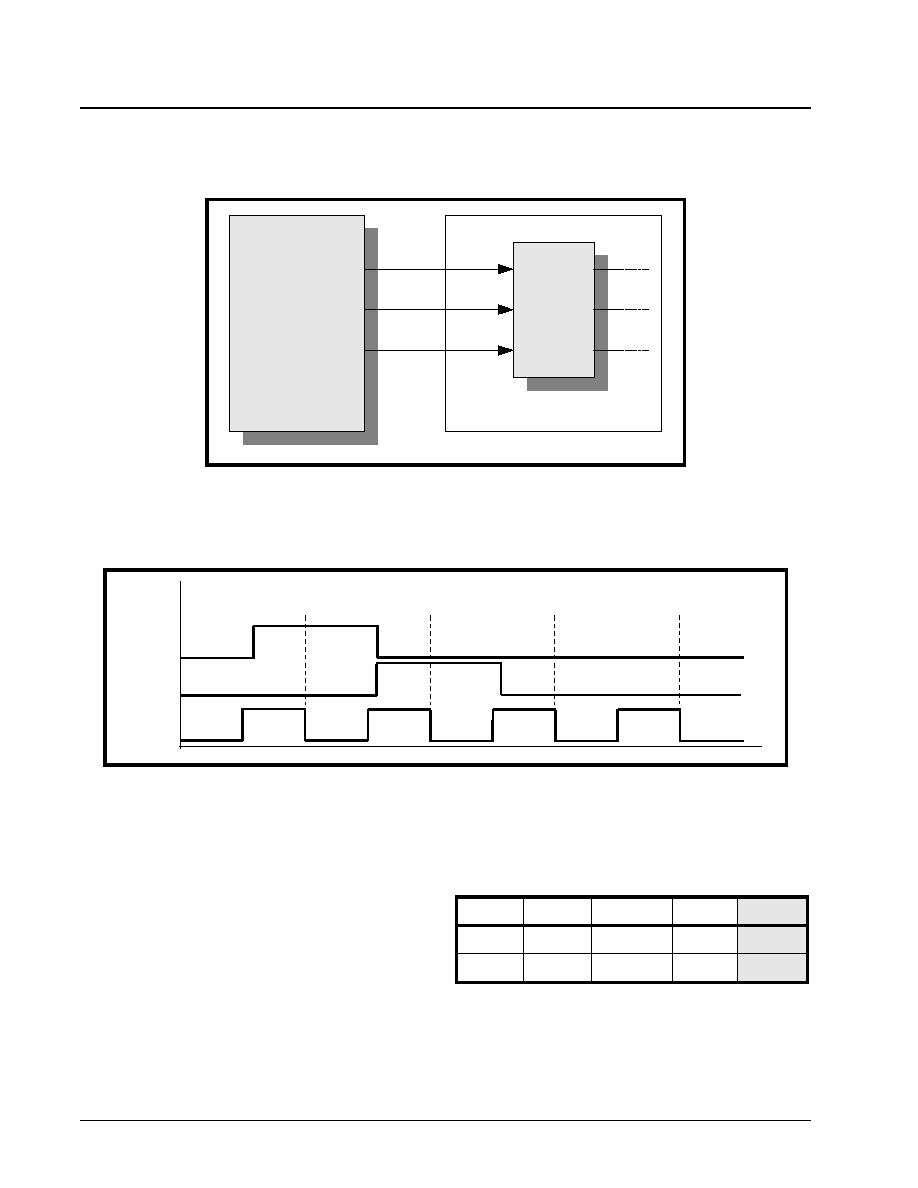
XRT7302
2 CHANNEL E3/DS3/STS-1 LINE INTERFACE UNIT
·Á
·Á
·Á
·Á
PRELIMINARY
REV. 1.1.6
26
The manner that the LIU handles Dual-Rail data is
described below and illustrated in Figure 8. The
Transmit Section of a Channel typically samples the
data on the TPData and TNData input pins on the fall-
ing edge of TxClk(n).
TxClk(n) is the clock signal that is of the selected data
rate frequency for E3 = 34.368 MHz, DS3 = 44.736
MHz and STS-1 = 51.84 MHz. If the Transmit Section
samples a "1" on the TPData input pin, the Transmit
Section of the XRT7302 generates a positive polarity
pulse via the TTIP(n) and TRing(n) output pins across
a 1:1 transformer. If the Transmit Section samples a
"1" on the TNData input pin, then the Transmit Sec-
tion ultimately generates a negative polarity pulse via
the TTIP(n) and TRing(n) output pins across a 1:1
transformer.
2.1.2
Configure Channel(n) to accept Single-
Rail Data from the Terminal Equipment
To transmit data in a Single-Rail data from the Termi-
nal Equipment, configure the XRT7302 in the HOST
Mode.
Write a "1" into the TxBin(n) (TRANSMIT BINary) bit-
field of Command Register CR1-(n) shown below.
N
OTE
: Please refer to Table 2 for the Address of the individ-
ual Channel(n).
The Transmit Section of each channel samples this
input pin on the falling edge of the TxClk(n) clock sig-
nal and encodes this data into the appropriate bipolar
line signal across the TTIP(n) and TRing(n) output
pins.
N
OTES
:
F
IGURE
7. T
HE
TYPICAL
INTERFACE
FOR
D
ATA
T
RANSMISSION
IN
D
UAL
-R
AIL
F
ORMAT
FROM
THE
T
RANSMITTING
T
ERMINAL
E
QUIPMENT
TO
THE
T
RANSMIT
S
ECTION
OF
A
CHANNEL
OF
THE
XRT7302
Terminal
Equipment
(E3/DS3 or STS-1
Framer)
E x a r E 3 / D S 3 / S T S - 1 L I U
Transmit
Logic
Block
T x P O S
T x N E G
TxLineClk
T P D a t a
T N D a t a
TxClk
F
IGURE
8. H
OW
THE
XRT7302 S
AMPLES
THE
DATA
ON
THE
TPD
ATA
AND
TND
ATA
INPUT
PINS
TxClk
TPData
TNData
Data 1 1 0
COMMAND REGISTER CR1-(N)
D4
D3
D2
D1
D0
TxOFF(n)
TAOS(n) TxClkINV(n) TxLEV(n)
TxBin(n)
X
X
X
X
1

·Á
·Á
·Á
·Á
2 CHANNEL E3/DS3/STS-1 LINE INTERFACE UNIT
XRT7302
PRELIMINARY
REV. 1.1.6
27
1. In this mode the Transmit Logic Block ignores the
TNData input pin.
2. If the Transmit Section of a given channel is config-
ured to accept Single-Rail data from the Terminal
Equipment, the B3ZS/HDB3 Encoder must be
enabled.
Figure 9 illustrates the behavior of the TPData and
TxClk(n) signals when the Transmit Logic Block has
been configured to accept Single-Rail data from the
Terminal Equipment.
2.2
T
HE
T
RANSMIT
C
LOCK
D
UTY
C
YCLE
A
DJUST
C
IR
-
CUITRY
The on-chip Pulse-Shaping circuitry in the Transmit
Section of each Channel of the XRT7302 generates
pulses of the appropriate shapes and width to meet
the applicable pulse template requirements. The
widths of these output pulses are defined by the width
of the half-period pulses in the TxClk(n) signal.
However, if the widths of the pulses in the TxClk(n)
clock signal are allowed to vary significantly, this
could jeopardize the chip's ability to generate Trans-
mit Output pulses of the appropriate width, thereby
not meeting the Pulse Template requirement specifi-
cation. Consequently, the chip's ability to generate
compliant pulses could depend upon the duty cycle of
the clock signal applied to the TxClk(n) input pin.
The Transmit Clock Duty Cycle Adjust Circuitry ac-
cepts clock pulses via the TxClk(n) input pin at duty
cycles ranging from 30% to 70% and converts them
to a 50% duty cycle.
2.3
T
HE
HDB3/B3ZS E
NCODER
B
LOCK
The purpose of the HDB3/B3ZS Encoder Block is to
aid in the Clock Recovery process at the Remote Ter-
minal Equipment by ensuring an upper limit on the
number of consecutive zeros that can exist in the line
signal.
2.3.1
B3ZS Encoding
If the XRT7302 has been configured to operate in the
DS3 or SONET STS-1 Modes, the HDB3/B3ZS En-
coder blocks operate in the B3ZS Mode. When the
Encoder is operating in this mode it parses through
and searches the Transmit Binary Data Stream from
the Transmit Logic Block for the occurrence of three
(3) consecutive zeros (e.g., "000"). If the B3ZS En-
coder finds an occurrence of three consecutive zeros,
then it substitutes these three "0's" with either a "00V"
or a "B0V" pattern.
"B" represents a Bipolar pulse that is compliant with
the Alternating Polarity requirements of the AMI (Al-
ternate Mark Inversion) line code.
"V" represents a Bipolar Violation (e.g., a Bipolar
pulse that violates the Alternating Polarity require-
ments of the AMI line code).
The B3ZS Encoder decides whether to substitute
with either the "00V" or the "B0V" pattern in order to
insure that an odd number of Bipolar pulses exist be-
tween any two consecutive violation pulses.
Figure 10 illustrates the B3ZS Encoder at work with
two separate strings of three or more consecutive ze-
ros.
F
IGURE
9. T
HE
B
EHAVIOR
OF
THE
TPD
ATA
AND
T
X
C
LK
I
NPUT
S
IGNALS
WHILE
THE
T
RANSMIT
L
OGIC
B
LOCK
IS
A
CCEPTING
S
INGLE
-R
AIL
D
ATA
FROM
THE
T
ERMINAL
E
QUIPMENT
TxClk
TPData
Data 1 1 0

XRT7302
2 CHANNEL E3/DS3/STS-1 LINE INTERFACE UNIT
·Á
·Á
·Á
·Á
PRELIMINARY
REV. 1.1.6
28
2.3.2
HDB3 Encoding
If the XRT7302 has been configured to operate in the
E3 Mode, the HDB3/B3ZS Encoder blocks operate in
the HDB3 Mode. When the Encoder is operating in
this mode it parses through and searches the Trans-
mit Data Stream from the Transmit Logic Block for the
occurrence of four (4) consecutive zeros ("0000"). If
the HDB3 Encoder finds an occurrence of four con-
secutive zeros then it substitutes these four "0's" with
either a "000V" or a "B00V" pattern. The HDB3 En-
coder decides whether to substitute with either the
"000V" or the "B00V" pattern in order to insure that an
odd number of Bipolar pulses exist between any two
consecutive violation pulses.
Figure 11 illustrates the HDB3 Encoder at work with
two separate strings of four or more consecutive ze-
ros.
2.3.3
Disabling the HDB3/B3ZS Encoder
The XRT7302 HDB3/B3ZS Encoder can be disabled
by two methods.
a. Operating in the Hardware Mode.
The HBD3/B3ZS Encoder blocks of all channels
are disabled by setting the ENDECDIS (Encoder/
Decoder Disable) input pin to "0".
N
OTE
: By executing this step the HDB3/B3ZS Encoder and
Decoder blocks in all channels of the XRT7302 are globally
disabled.
b. Operating in the HOST Mode.
When the XRT7302 is operating in the HOST Mode
the HDB3/B3ZS Encoders in each channel can be
individually enabled or disabled. Disable the
HDB3/B3ZS Encoder block in Channel(n) by setting
F
IGURE
10. A
N
E
XAMPLE
OF
B3ZS E
NCODING
1
1
1
0
0
0
0
0
1
1
1
1
1
1
1
1
1
1
1
1
1
0
0
0
0
0
0
0
B
0
V
0
0
V
Line Signal
TxClk
TNData
TPData
Data
F
IGURE
11. A
N
E
XAMPLE
OF
HDB3 E
NCODING
1
1
1
0
0
0
0
0
0
1
1
1
1
1
1
1
1
1
1
0
1
0
0
0
0
0
0
0
B
0
V
0
0
V
Line Signal
TxClk
TNData
TPData
Data
0
0
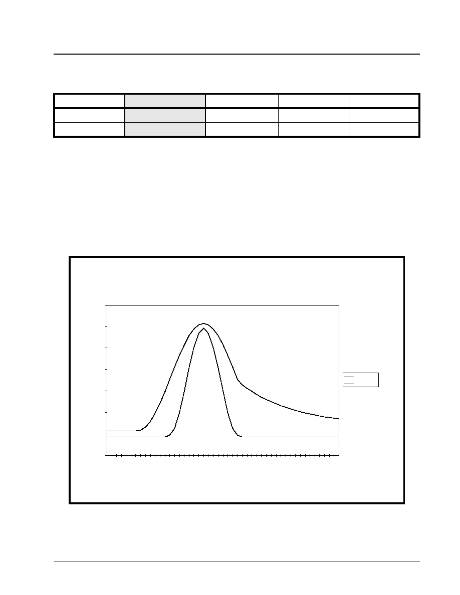
·Á
·Á
·Á
·Á
2 CHANNEL E3/DS3/STS-1 LINE INTERFACE UNIT
XRT7302
PRELIMINARY
REV. 1.1.6
29
the ENDECDIS(n) bit-field in Command Register
(CR2-(n)), to "1".
If either of these two methods is used to disable the
HDB3/B3ZS Encoder, the LIU transmits the data as
received via the TPData and TNData input pins.
2.4
T
HE
T
RANSMIT
P
ULSE
S
HAPING
C
IRCUITRY
The Transmit Pulse Shaper Circuitry consists of a
Transmit Line Build-Out circuit which can be enabled
or disabled by setting the TxLEV(n) input pin or Tx-
LEV(n) bit-field to "High" or "Low". The purpose of
the Transmit Line Build-Out circuit is to permit config-
uration of each channel in the XRT7302 to transmit
an output pulse which is compliant to either of the fol-
lowing pulse template requirements when measured
at the Digital Cross Connect System. Each of these
Bellcore specifications state that the cable length be-
tween the Transmit Output and the Digital Cross Con-
nect system can range anywhere from 0 to 450 feet.
The Isolated DSX-3 Pulse Template Requirement per
Bellcore GR-499-CORE is illustrated in Figure 12 and
the Isolated STSX-1 Pulse Template Requirement
per Bellcore GR-253-CORE is illustrated in Figure 13.
COMMAND REGISTER CR2-(N)
D4
D3
D2
D1
D0
Reserved
ENDECDIS(n)
ALOSDIS(n)
DLOSDIS(n)
REQEN(n)
X
1
X
X
X
F
IGURE
12. T
HE
B
ELLCORE
GR-499-CORE T
RANSMIT
O
UTPUT
P
ULSE
T
EMPLATE
FOR
DS3 A
PPLICATIONS
D S 3 P u ls e T e m p la te
-0.2
0
0.2
0.4
0.6
0.8
1
1.2
-1
-0
.9
-0
.8
-0
.7
-0
.6
-0
.5
-0
.4
-0
.3
-0
.2
-0
.1
0
0.
1
0.
2
0.
3
0.
4
0.
5
0.
6
0.
7
0.
8
0.
9
1
1.
1
1.
2
1.
3
1.
4
T i m e , i n U I
N
o
r
m
a
l
i
z
e
d
A
m
pl
i
t
ude
Lower Curve
Upper Curve

XRT7302
2 CHANNEL E3/DS3/STS-1 LINE INTERFACE UNIT
·Á
·Á
·Á
·Á
PRELIMINARY
REV. 1.1.6
30
.
2.4.1
Enabling the Transmit Line Build-Out Cir-
cuit
If the Transmit Line Build-Out Circuit is enabled, the
Transmit Section of Channel(n) of the XRT7302 out-
puts shaped pulses onto the line via the TTIP(n) and
TRing(n) output pins.
Enable the Transmit Line Build-Out circuit for each
channel in the XRT7302 by doing the following:
a. Operating in the Hardware Mode
Set the TxLEV(n) input pin to "Low"
b. Operating in the HOST Mode
Set the TxLEV(n) bit-field to "0".
2.4.2
Disabling the Transmit Line Build-Out Cir-
cuit
If the Transmit Line Build-Out circuit is disabled, the
XRT7302 outputs partially-shaped pulses onto the
line via the TTIP(n) and TRing(n) output pins.
To disable the Transmit Line Build-Out circuit, do the
following:
a. Operating in the Hardware Mode
Set the TxLEV(n) input pin to "High".
b. Operating in the HOST Mode
Set the TxLEV(n) bit-field to "1" as illustrated below.
F
IGURE
13. T
HE
B
ELLCORE
GR-253-CORE T
RANSMIT
O
UTPUT
P
ULSE
T
EMPLATE
FOR
SONET STS-1 A
PPLI
-
CATIONS
S T S -1 P uls e T e m p la te
-0.2
0
0.2
0.4
0.6
0.8
1
1.2
-1
-0
.9
-0
.8
-0
.7
-0
.6
-0
.5
-0
.4
-0
.3
-0
.2
-0
.1
0
0.
1
0.
2
0.
3
0.
4
0.
5
0.
6
0.
7
0.
8
0.
9
1
1.
1
1.
2
1.
3
1.
4
Tim e , in UI
N
o
r
m
al
i
z
ed
A
m
p
l
i
t
u
d
e
Lower Curve
Upper Curve
COMMAND REGISTER CR1-(N)
D4
D3
D2
D1
D0
TxOFF(n)
TAOS(n)
TxClkINV(n)
TxLEV(n)
TxBIN(n)
0
X
X
0
X

·Á
·Á
·Á
·Á
2 CHANNEL E3/DS3/STS-1 LINE INTERFACE UNIT
XRT7302
PRELIMINARY
REV. 1.1.6
31
2.4.3
Design Guideline for Setting the Transmit
Line Build-Out Circuit
The TxLEV(n) input pins or bit-fields should be set
based upon the overall cable length between the
Transmitting Terminal and the Digital Cross Connect
system where the pulse template measurements are
made.
If the cable length between the Transmitting Ter-
minal and the DSX-3 or STSX-1 is less than 225
feet, enable the Transmit Line Build-Out circuit by
setting the TxLEV(n) input pin or bit-field to "0".
N
OTE
: In this case, the configured channel outputs shaped
(e.g., not square-wave) pulses onto the line via its TTIP(n)
and TRing(n) output pins. The shape of this output pulse is
such that it complies with the pulse template requirements
even when subjected to cable loss ranging from 0 to 225
feet.
If the cable length between the Transmitting Ter-
minal and the DSX-3 or STSX-1 is greater than 225
feet, disable the Transmit Line Build-Out circuit
by setting the TxLEV(n) input pin or bit-field to
"1".
N
OTE
: In this case, the configured channel in the XRT7302
outputs partially-shaped pulses onto the line via the TTIP(n)
and TRing(n) output pins. The cable loss that these pulses
experience over long cable lengths (e.g., greater than 225
feet) causes these pulses to be properly shaped and com-
ply with the appropriate pulse template requirement.
2.4.4
The Transmit Line Build-Out Circuit and
E3 Applications
The ITU-T G.703 Pulse Template Requirements for
E3 states that the E3 transmit output pulse should be
measured at the Secondary Side of the Transmit Out-
put Transformer for Pulse Template compliance. In
other words, there is no Digital Cross Connect Sys-
tem pulse template requirement for E3. Consequent-
ly, the Transmit Line Build-Out circuit in a given Chan-
nel in the XRT7302 is disabled whenever that channel
has been configured to operate in the E3 Mode.
2.5
I
NTERFACING
THE
T
RANSMIT
S
ECTIONS
OF
THE
XRT7302
TO
THE
L
INE
The E3, DS3 and SONET STS-1 specification docu-
ments all state that line signals transmitted over coax-
ial cable are to be terminated with 75 Ohm resistor.
Interface the Transmit Section of the XRT7302 in the
manner illustrated in Figure 14 to accomplish this.
COMMAND REGISTER CR1-(N)
D4
D3
D2
D1
D0
TxOFF(n)
TAOS(n)
TxClkINV(n)
TxLEV(n)
TxBin(n)
0
X
X
1
X
F
IGURE
14. R
ECOMMENDED
S
CHEMATIC
FOR
I
NTERFACING
THE
T
RANSMIT
S
ECTION
OF
THE
XRT7302
TO
THE
L
INE
R 1
31.6
R 2
31.6
Channel (n)
T x P O S ( n )
T x N E G ( n )
TxLineClk(n)
TTIP(n)
TRing(n)
T P D a t a ( n )
T N D a t a ( n )
TxClk(n)
Only One Channel Shown
1:1
J1
B N C

XRT7302
2 CHANNEL E3/DS3/STS-1 LINE INTERFACE UNIT
·Á
·Á
·Á
·Á
PRELIMINARY
REV. 1.1.6
32
TRANSFORMER VENDOR INFORMATION
Pulse
Corporate Office
12220 World Trade Drive
San Diego, CA 92128
Tel: (619)-674-8100
FAX: (619)-674-8262
Europe
1 & 2 Huxley Road
The Surrey Research Park
Guildford, Surrey GU2 5RE
United Kingdom
Tel: 44-1483-401700
FAX: 44-1483-401701
Asia
150 Kampong Ampat
#07-01/02
KA Centre
Singapore 368324
Tel: 65-287-8998
FAX: 65-280-0080
3.0
THE RECEIVE SECTION
Figure 6 indicates that the Receive Section in the
XRT7302 consists of the following blocks:
∑ AGC/Equalizer
∑ Peak Detector
∑ Slicer
∑ Clock Recovery PLL
∑ Data Recovery
∑ HDB3/B3ZS Decoder
The purpose of each Receive Section of the
XRT7302 is to take an incoming attenuated/distorted
bipolar signal from the line and encode it back into
the TTL/CMOS format where it can be received and
processed by the Terminal Equipment.
3.1
I
NTERFACING
THE
R
ECEIVE
S
ECTIONS
OF
THE
XRT7302
TO
THE
L
INE
The design of the Receive Circuitry in the XRT7302
allows for transformer-coupling or capacitive-coupling
of the Receive Section to the line. As mentioned ear-
lier, the specification documents for E3, DS3 and
STS-1 all specify 75 Ohm termination loads when
transmitting over coaxial cable. The recommended
method of Transformer-Coupling the Receive Section
of the XRT7302 to the line is shown in Figure 15 and
the Capacitive-Coupling method is shown in Figure
16.
Transformer Recommendations
P
ARAMETER
V
ALUE
Turns Ratio
1:1
Primary Inductance
4µH
Isolation Voltage
1500Vrms
Leakage Inductance
0.06µH
P
ART
#
I
NSULATION
P
ACKAGE
T
YPE
PE-68629
3000V
Large Thru-Hole
PE-65966
1500V
Small Thru-Hole
PE-65967
1500V
Small SMT
T3001
1500V
Small SMT

·Á
·Á
·Á
·Á
2 CHANNEL E3/DS3/STS-1 LINE INTERFACE UNIT
XRT7302
PRELIMINARY
REV. 1.1.6
33
F
IGURE
15. R
ECOMMENDED
S
CHEMATIC
FOR
T
RANSFORMER
-C
OUPLING
THE
R
ECEIVE
S
ECTION
OF
THE
XRT7302
TO
THE
L
INE
J 1
B N C
T 1
1:1
R 1
37.5
R 2
37.5
Channel (n)
R x P O S ( n )
R x N E G ( n )
RxClk(n)
RTIP(n)
RRing(n)
R P O S ( n )
R N E G ( n )
RxClk(n)
C 1
0.01uf
O n l y O n e C h a n n e l S h o w n
F
IGURE
16. R
ECOMMENDED
S
CHEMATIC
FOR
C
APACITIVE
-C
OUPLING
THE
R
ECEIVE
S
ECTION
OF
THE
XRT7302
TO
THE
L
INE
R 1
7 5
J 1
B N C
Channel (n)
R x P O S ( n )
R x N E G ( n )
RxClk(n)
RTIP(n)
RRing(n)
R P O S ( n )
R N E G ( n )
RxClk(n)
C 1
0.01uf
O n l y O n e C h a n n e l S h o w n
C 2
0.01uf

XRT7302
2 CHANNEL E3/DS3/STS-1 LINE INTERFACE UNIT
·Á
·Á
·Á
·Á
PRELIMINARY
REV. 1.1.6
34
3.2
T
HE
R
ECEIVE
E
QUALIZER
B
LOCK
The purpose of this block is to equalize the incoming
distorted signal due to cable loss. The Receive
Equalizer attempts to restore the shape of the line
signal so that the transmitted data and clock can be
recovered reliably.
∑ Design Considerations for DS3 and STS-1
Applications
When installing equipment into environments depict-
ed in Figure 17, we recommend that the Receive
Equalizer be enabled by setting the REQEN(n) input
pin for Channel(n) or the respective bit-fields to "1".
The only time that the Receive Equalizer should be
disabled is when an off-chip equalizer is in the Re-
ceive path between the Digital Cross-Connect system
and the RTIP/RRing input pins, or in applications
where the Receiver is monitoring the transmit output
signal directly.
∑ Design Considerations for E3 Applications or if
the Overall Cable Length is known
Figure 17 indicates the following:
a. The length of cable between the Transmitting Ter-
minal and the Digital Cross-Connect system can
range between 0 and 450 feet.
b. The length of cable between the Digital Cross-Con-
nect system and the Receive Terminal can range be-
tween 0 and 450 feet.
Consequently, the overall cable length between the
Transmitting Terminal and the Receiving Terminal can
range between very short cable length (e.g., near 0
feet) up to 900 feet.
If during System Installation the overall cable length is
known, to optimize the performance of the XRT7302
in terms of receive jitter performance, etc., enable or
disable the Receive Equalizer based upon the follow-
ing recommendations:
The Receive Equalizer should be turned ON if the
Receive Section of a given channel is going to re-
F
IGURE
17. T
HE
T
YPICAL
A
PPLICATION
FOR
THE
S
YSTEM
I
NSTALLER
Digital Cross-Connect
System
Transmitting
Terminal
Receiving
Terminal
0 to 450 feet of Cable
Pulses that are
compliant to the
Isolated DSX-3 or
STSX-1 Pulse Template
Requirement
0 to 450 feet of
Cable
DSX-3
or
STSX-1

·Á
·Á
·Á
·Á
2 CHANNEL E3/DS3/STS-1 LINE INTERFACE UNIT
XRT7302
PRELIMINARY
REV. 1.1.6
35
ceive a line signal with an overall cable length of 300
feet or greater. Conversely, turn OFF the Receive
Equalizer if the Receive Section of a given channel is
going to receive a line signal with an overall cable
length of less than 300 feet.
N
OTES
:
1. If the Receive Equalizer block is turned ON when it
is receiving a line signal over short cable length the
received line signal may be over-equalized, which
could degrade performance by increasing the
amount of jitter that exists in the recovered data
and clock signals or by creating bit-errors.
2. The Receive Equalizer has been designed to
counter the frequency-dependent cable loss that a
line signal experiences as it travels from the trans-
mitting terminal to the receiving terminal. However,
the Receive Equalizer was not designed to counter
flat loss where all of the Fourier frequency compo-
nents within the line signal are subject to the same
amount of attenuation. Flat loss is handled by the
AGC block.
Disable the Receive Equalizer block by doing either of
the following:
a. Operating in the Hardware Mode
Set the REQEN(n) input pin "Low".
b. Operating in the HOST Mode
Write a "0" to the REQEN(n) bit-field in Command
Register CR2.
3.3
P
EAK
D
ETECTOR
AND
S
LICER
After the incoming line signal has passed through the
Receive Equalizer block, it is routed to the Slicer
block. The Slicer block quantifies a given bit-period
(or symbol) within the incoming line signal as either a
"1" or a "0".
3.4
C
LOCK
R
ECOVERY
PLL
The purpose of the Clock Recovery PLL is to track
the incoming Dual-Rail data stream and to derive and
generate a recovered clock signal.
It is important to note that the Clock Recovery PLL re-
quires a line rate clock signal at the ExClk input pin.
The Clock Recovery PLL operates in one of two
modes:
∑ The Training Mode
∑ The Data/Clock Recovery Mode
3.4.1
The Training Mode
If a given channel in the XRT7302 is not receiving a
line signal via the RTIP and RRing input pins, or if the
frequency difference between the line signal and that
applied via the ExClk input pin exceeds 0.5%, the
channel operates in the Training Mode. When the
channel is operating in the Training Mode, it does the
following:
a. Declare a Loss of Lock indication by toggling its
respective RLOL(n) output pin "High".
b. Output a clock signal via the RxClk(n) output pin
which is derived from the signal applied to the
EXClk(n) input pin.
3.4.2
The Data/Clock Recovery Mode
If the frequency difference between the line signal
and that applied via the ExClk input pin is less than
0.5%, the channel operates in the Data/Clock Recov-
ery mode. In this mode, the Clock Recovery PLL
locks onto the line signal via the RTIP and RRing in-
put pins.
3.5
T
HE
HDB3/B3ZS D
ECODER
The Remote Transmitting Terminal typically encodes
the line signal into some sort of Zero Suppression
Line Code (e.g., HDB3 for E3 and B3ZS for DS3 and
STS-1). The purpose of this encoding activity was to
aid in the Clock Recovery process of this data from
the Near-End Receiving Terminal. However, once the
data has made it across the E3, DS3 or STS-1 Trans-
port Medium and has been recovered by the Clock
Recovery PLL, it is now necessary to restore the orig-
inal content of the data. The purpose of the HDB3/
B3ZS Decoding block is to restore the data transmit-
ted over the E3, DS3 or STS-1 line to its original con-
tent prior to Zero Suppression Coding.
3.5.1
B3ZS Decoding DS3/STS-1 Applications
If the XRT7302 is configured to operate in the DS3 or
STS-1 Modes, then the HDB3/B3ZS Decoding Blocks
perform B3ZS Decoding. When the Decoders are
operating in this mode, each of the Decoders parses
through its respective incoming Dual-Rail data and
COMMAND REGISTER CR2_(N)
D4
D3
D2
D1
D0
RESERVED
ENDECDIS(n)
ALOSDIS(n)
DLOSDIS(n)
REQEN(n)
X
X
X
X
0

XRT7302
2 CHANNEL E3/DS3/STS-1 LINE INTERFACE UNIT
·Á
·Á
·Á
·Á
PRELIMINARY
REV. 1.1.6
36
checks for the occurrence of either a "00V" or a "B0V"
pattern. If the B3ZS Decoder detects this particular
pattern, it substitutes these bits with a "000" pattern.
N
OTE
: If the B3ZS Decoder detects any bipolar violations
that is not in accordance with theB3ZS Line Code format or
if the B3ZS Decoder detects a string of 3 or more consecu-
tive "0's" in the incoming line signal, the B3ZS Decoder
flags this event as a Line Code Violation by pulsing the LCV
output pin "High".
Figure 18 illustrates the B3ZS Decoder at work with
two separate Zero Suppression patterns in the in-
coming Dual-Rail Data Stream.
3.5.2
HDB3 Decoding E3 Applications
If the XRT7302 is configured to operate in the E3
Mode, then each of the HDB3/B3ZS Decoding Blocks
performs HDB3 Decoding. When the Decoders are
operating in this mode, they each parse through the
incoming Dual-Rail data and check for the occurrence
of either a "000V" or a "B00V" pattern. If the HDB3
Decoder detects this particular pattern, it substitutes
these bits with a "0000" pattern.
Figure 19 illustrates the HDB3 Decoder at work with
two separate Zero Suppression patterns in the in-
coming Dual-Rail Data Stream.
N
OTE
: If the HDB3 Decoder detects any bipolar violation
(e.g., "V") pulses that is not in accordance with the HDB3
Line Code format, or if the HDB3 Decoder detects a string
of 4 or more "0's" in the incoming line signal, the HDB3
Decoder flags this event as a Line Code Violation by puls-
ing the LCV output pin "High".
3.5.3
Configuring the HDB3/B3ZS Decoder
The XRT7302 can enable or disable the HDB3/B3ZS
Decoder blocks of each Channel by either of the fol-
lowing means.
a. Operating in the HOST Mode
Enable the HDB3/B3ZS Decoder block of Channel(n)
by writing a "0" into the ENDECDIS(n) bit-field in
Command Register CR2-(n).
F
IGURE
18. A
N
E
XAMPLE
OF
B3ZS D
ECODING
Line Signal
RxClk
Data
1
1
1
0
0
0
0
0
1
1
1
1
1
1
1
1
1
1
1
1
1
0
0
0
0
0
0
0
0
R P O S
R N E G
B
0
V
0
V
0
F
IGURE
19. A
N
E
XAMPLE
OF
HDB3 D
ECODING
B
0
V
0
0
V
Line Signal
0
0
RxClk
Data
1
1
1
0
0
0
0
0
0
1
1
1
1
1
1
1
1
1
1
0
1
0
0
0
0
0
0
0
0
R P O S
R N E G

·Á
·Á
·Á
·Á
2 CHANNEL E3/DS3/STS-1 LINE INTERFACE UNIT
XRT7302
PRELIMINARY
REV. 1.1.6
37
b. Operating in the Hardware Mode
To globally enable all HDB3/B3ZS Decoder blocks in
the XRT7302, pull the ENDEC_DIS input pin "Low".
To globally disable all HDB3/B3ZS Decoder blocks in
the XRT7302 and configure the XRT7302 to transmit
and receive in an AMI format, pull the ENDEC_DIS
input pin "High".
3.6
LOS D
ECLARATION
/C
LEARANCE
Each channel of the XRT7302 contains circuitry that
monitors the following two parameters associated
with the incoming line signals.
1. The amplitude of the incoming line signal via the
RTIP and RRing inputs.
2. The number of pulses detected in the incoming
line signal within a certain amount of time.
If a given channel of the XRT7302 determines that
the incoming line signal is missing due to either insuf-
ficient amplitude or a lack of pulses in the incoming
line signal, it declares a Loss of Signal (LOS) condi-
tion. The channel declares the LOS condition by tog-
gling its respective RLOS(n) output pin "High" and by
setting its corresponding RLOS(n) bit field in Com-
mand Register 0 or Command Register 8 to "1".
Conversely, if the channel determines that the incom-
ing line signal has been restored (e.g., there is suffi-
cient amplitude and pulses in the incoming line sig-
nal), it clears the LOS condition by toggling its re-
spective RLOS(n) output pin "Low" and setting its cor-
responding RLOS(n) bit-field to "0".
In general, the LOS Declaration/Clearance scheme
that is employed in the XRT7302 is based upon ITU-T
Recommendation G.775 for both E3 and DS3 appli-
cations.
3.6.1
The LOS Declaration/Clearance Criteria
for E3 Applications
When the XRT7302 is operating in the E3 Mode, a
given channel declares an LOS Condition if its re-
ceive line signal amplitude drops to -35dB or below.
Further, the channel clears the LOS Condition if its
receive line signal amplitude rises back to -15dB or
above. Figure 20 illustrates the signal levels at which
each channel of the XRT7302 declares and clears
LOS.
COMMAND REGISTER CR2-(N)
D4
D3
D2
D1
D0
Reserved
ENDEC_DIS
ALOSDIS(n)
DLOSDIS(n)
REQEN(n)
X
0
X
X
1

XRT7302
2 CHANNEL E3/DS3/STS-1 LINE INTERFACE UNIT
·Á
·Á
·Á
·Á
PRELIMINARY
REV. 1.1.6
38
Timing Requirements associated with Declaring
and Clearing the LOS Indicator
The XRT7302 was designed to meet the ITU-T G.775
specification timing requirements for declaring and
clearing the LOS indicator. In particular, a channel of
the XRT7302 declares an LOS between 10 and 255
UI (or E3 bit-periods) after the actual time the LOS
condition occurred. The channel clears the LOS indi-
cator within 10 to 255 UI after restoration of the in-
coming line signal. Figure 21 illustrates the LOS Dec-
laration and Clearance behavior in response to the
Loss of Signal event and then the restoration of the
signal.
F
IGURE
20. T
HE
S
IGNAL
L
EVELS
AT
WHICH
THE
XRT7302
DECLARES
AND
CLEARS
LOS
0 dB
-12 dB
-15dB
-35dB
Maximum Cable Loss for E3
LOS Signal Must be Declared
LOS Signal Must be Cleared
LOS Signal may be Cleared or Declared
F
IGURE
21. T
HE
B
EHAVIOR
THE
LOS O
UTPUT
I
NDICATOR
IN
RESPONSE
TO
THE
L
OSS
OF
S
IGNAL
AND
THE
R
ESTO
-
RATION
OF
S
IGNAL
Actual Occurrence
of LOS Condition
Line Signal
is Restored
Time Range for
LOS Declaration
Time Range for
LOS Clearance
G.775
Compliance
G.775
Compliance
0 UI
10 UI
0 UI
10 UI
255 UI
255 UI
RTIP/
RRing
RLOS Output Pin
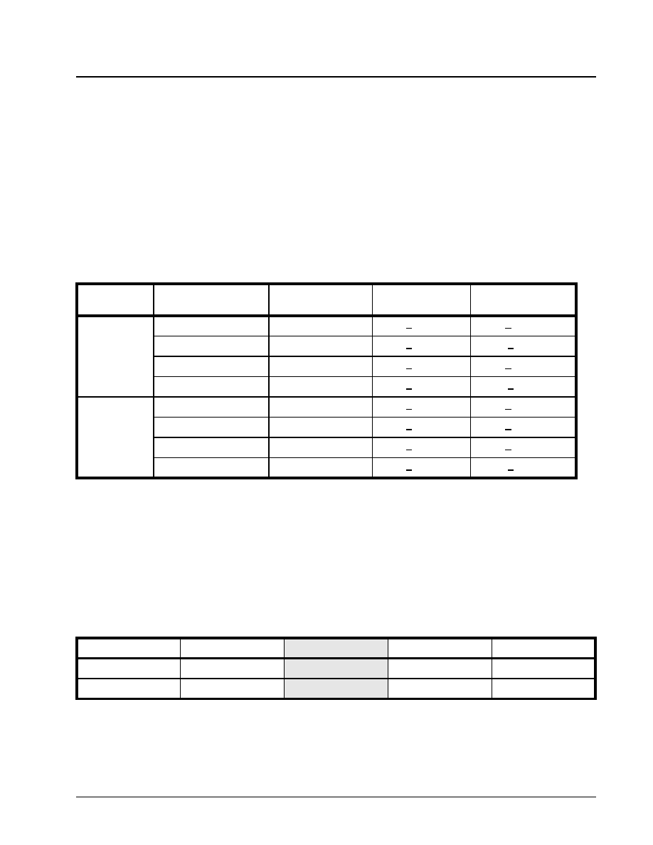
·Á
·Á
·Á
·Á
2 CHANNEL E3/DS3/STS-1 LINE INTERFACE UNIT
XRT7302
PRELIMINARY
REV. 1.1.6
39
3.6.2
The LOS Declaration/Clearance Criteria
for DS3 and STS-1 Applications
When the XRT7302 is operating in the DS3 or STS-1
Mode, each channel in the XRT7302 declares and
clears LOS based upon the following two criteria:
∑ Analog LOS (ALOS) Declaration/Clearance Crite-
ria
∑ Digital LOS (DLOS) Declaration/Clearance Crite-
ria
In the DS3 Mode, the LOS output (RLOS) is simply
the logical "OR" of the ALOS and DLOS states.
1. The Analog LOS (ALOS) Declaration/Clearance
Criteria
A channel in the XRT7302 declares an Analog LOS
(ALOS(n)) Condition if the amplitude of the incoming
line signal drops below a specific amplitude as de-
fined by the voltage at the LOSTHR input pin and
whether the Receive Equalizer is enabled or not.
Table 5 presents the various voltage levels at the
LOSTHR input pin, the state of the Receive Equalizer,
and the corresponding ALOS (Analog LOS) threshold
amplitudes.
Declaring ALOS
A Channel(n) in the XRT7302 declares ALOS(n)
whenever the amplitude of the receive line signal falls
below the signal levels to declare ALOS, as specified
in Table 5.
Clearing ALOS(n)
A Channel(n) clears ALOS(n) whenever the ampli-
tude of the receive line signal increases above the
signal levels to declare ALOS, as specified in Table 5.
There is approximately a 2dB hysteresis in the re-
ceived signal level that exists between declaring and
clearing ALOS(n) in order to prevent chattering in the
RLOS(n) output signal.
Monitoring the State of ALOS(n)
If the XRT7302 is operating in the HOST Mode, the
state of ALOS(n) of Channel(n) can be polled or mon-
itored by reading in the contents of Command Regis-
ter CR0.
If the ALOS(n) bit-field contains a "1", then the corre-
sponding Channel(n) is currently declaring an ALOS
condition. If the ALOS(n) bit-field contains a "0", then
the channel is not currently declaring an ALOS condi-
tion.
T
ABLE
5: T
HE
ALOS (A
NALOG
LOS) D
ECLARATION
AND
C
LEARANCE
T
HRESHOLDS
FOR
A
GIVEN
SETTING
OF
LOSTHR
AND
REQEN
FOR
DS3
AND
STS-1 A
PPLICATIONS
A
PPLICATION
REQEN S
ETTING
LOSTHR S
ETTING
S
IGNAL
L
EVEL
TO
D
ECLARE
ALOS
S
IGNAL
L
EVEL
TO
C
LEAR
ALOS
DS3
1
0
<55mV
>220mV
1
1
<22mV
>90mV
0
0
<35mV
>155mV
0
1
<17mV
>70mV
STS-1
1
0
<75mV
>270mV
1
1
<25mV
>115mV
0
0
<55mV
>210mV
0
1
<20mV
>90mV
COMMAND REGISTER CR0-(N)
D4
D3
D2
D1
D0
RLOL(n)
RLOS(n)
ALOS(n)
DLOS(n)
DMO(n)
Read Only
Read Only
Read Only
Read Only
Read Only
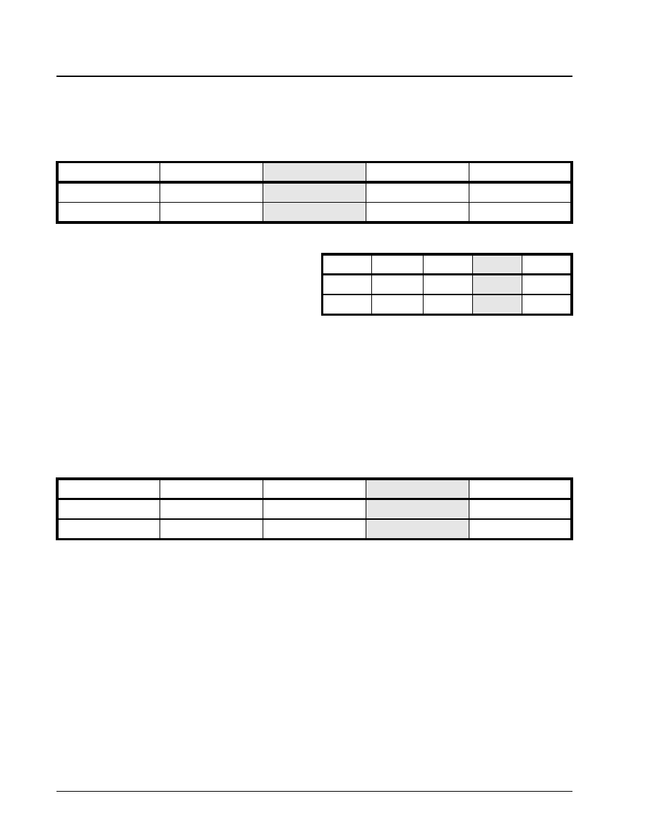
XRT7302
2 CHANNEL E3/DS3/STS-1 LINE INTERFACE UNIT
·Á
·Á
·Á
·Á
PRELIMINARY
REV. 1.1.6
40
Disabling the ALOS Detector
For debugging purposes it may be useful to disable
the ALOS Detector in the XRT7302. If the XRT7302
is operating in the HOST Mode, the ALOS Detector
can be disabled by writing a "1" into the ALOSDIS(n)
bit-field in Command Register CR2.
2. The Digital LOS (DLOS) Declaration/Clearance
Criteria
A given Channel(n) in the XRT7302 declares a Digital
LOS (DLOS(n)) condition if the XRT7302 detects
160±32 or more consecutive "0's" in the incoming da-
ta.
The channel clears DLOS if it detects four consecu-
tive sets of 32 bit-periods, each of which contains at
least 10 "1's" (e.g., average pulse density of greater
than 33%).
Monitoring the State of DLOS
If the XRT7302 is operating in the HOST Mode the
state of DLOS(n) of Channel(n) can be polled or mon-
itored by reading in the contents of Command Regis-
ter CR0.
If the DLOS(n) bit-field contains a "1", then the corre-
sponding Channel(n) is currently declaring a DLOS
condition. If the DLOS(n) bit-field contains a "0", the
Channel(n) is currently declaring the DLOS condition.
Disabling the DLOS Detector
For debugging purposes, it is useful to be able to dis-
able the DLOS(n) detector in the XRT7302. If the
XRT7302 is operating in the HOST Mode, the DLOS
Detector can be disabled by writing a "1" into the
DLOSDIS(n) bit-field of Command Register CR2.
N
OTE
: Setting both the ALOSDIS(n) and DLOSDIS(n) bit-
fields to "1" disables LOS Declaration by Channel(n).
3.6.3
Muting the Recovered Data while the LOS
is being Declared
In some applications it is not desirable for a channel
of the XRT7302 to recover data and route it to the Re-
ceiving Terminal while the channel is declaring an
LOS condition. Consequently, the XRT7302 includes
an LOS Muting feature. This feature if enabled caus-
es a given channel to halt transmission of the recov-
ered data to the Receiving Terminal while the LOS
condition is "true". In this case, the RPOS(n) and
RNEG(n) output pins are forced to "0". Once the LOS
condition has been cleared, the channel resumes
normal transmission of the recovered data to the Re-
ceiving Terminal.
This feature is available whenever the XRT7302 is
operating in the HOST or Hardware Mode.
a. Operating in the Hardware Mode.
To enable the MUTing upon LOS feature for all chan-
nels of the XRT7302, pull the LOSMUTEN output pin
"High".
b. Operating in the HOST Mode.
COMMAND REGISTER CR2-(N)
D4
D3
D2
D1
D0
Reserved
ENDECDIS(n)
ALOSDIS(n)
DLOSDIS(n)
REQEN(n)
X
X
1
X
X
COMMAND REGISTER CR0-(N)
D4
D3
D2
D1
D0
RLOL(n)
RLOS(n)
ALOS(n)
DLOS(n)
DMO(n)
Read Only Read Only Read Only Read Only Read Only
COMMAND REGISTER CR2-(N)
D4
D3
D2
D1
D0
Reserved
ENDECDIS(n)
ALOSDIS(n)
DLOSDIS(n)
REQEN(n)
X
X
X
1
X

·Á
·Á
·Á
·Á
2 CHANNEL E3/DS3/STS-1 LINE INTERFACE UNIT
XRT7302
PRELIMINARY
REV. 1.1.6
41
The MUTing upon LOS feature for each Channel can
be enabled by writing a "1" into the LOSMUT(n) bit-
field in Command Register 3.
N
OTES
:
1. This step only enables the MUTing upon LOS fea-
ture in Channel(n).
2. Each channel(n) automatically declares an LOS
(Loss of Signal) condition anytime it has been conf-
gured to operate in either the Analog Local Loop-
Back or Digital Local Loop-Back modes. To config-
ure the chip to operate in either of these modes,
disable the MUTing-upon-LOS feature.
3.7
R
OUTING
THE
R
ECOVERED
T
IMING
AND
D
ATA
I
NFORMATION
TO
THE
R
ECEIVING
T
ERMINAL
E
QUIPMENT
Each channel in the XRT7302 takes the Recovered
Timing and Data information, converts it into CMOS
levels and routes it to the Receiving Terminal Equip-
ment via the RPOS(n), RNEG(n) and RxClk(n) output
pins.
Each channel of the XRT7302 can deliver the recov-
ered data and clock information to the Receiving Ter-
minal in either a Single-Rail or Dual-Rail format.
3.7.1
Routing Dual-Rail Format Data to the
Receiving Terminal Equipment
Whenever a channel of the XRT7302 delivers Dual-
Rail format to the Terminal Equipment, it does so via
the following signals:
∑ RPOS(n)
∑ RNEG(n)
∑ RxClk(n)
Figure 22 illustrates the typical interface for the trans-
mission of data in a Dual-Rail Format from the Re-
ceive Section of a channel to the Receiving Terminal
Equipment
.
The manner that a given channel transmits Dual-Rail
data to the Receiving Terminal Equipment is de-
scribed below and illustrated in Figure 23. Each
Channel(n) of the XRT7302 typically updates the data
on the RPOS(n) and RNEG(n) output pins on the ris-
ing edge of RxClk(n).
COMMAND REGISTER CR3-(N)
D4
D3
D2
D1
D0
SR/(DR)_(n)
LOSMUT(n)
RxOFF(n)
RxClk(n)INV
Reserved
X
1
X
X
X
F
IGURE
22. T
HE
TYPICAL
INTERFACE
FOR
THE
T
RANSMISSION
OF
D
ATA
IN
A
D
UAL
-R
AIL
F
ORMAT
FROM
THE
R
ECEIVE
S
ECTION
OF
THE
XRT7302
TO
THE
R
ECEIVING
T
ERMINAL
E
QUIPMENT
Terminal
Equipment
(E3/DS3 or STS-1
Framer)
Terminal
Equipment
(E3/DS3 or STS-1
Framer)
Exar E3/DS3/STS-1 LIU
Receive
Logic
Block
Receive
Logic
Block
RxPOS
RxNEG
RxClk
RPOS
RNEG
RxClk

XRT7302
2 CHANNEL E3/DS3/STS-1 LINE INTERFACE UNIT
·Á
·Á
·Á
·Á
PRELIMINARY
REV. 1.1.6
42
RxClk(n) is the Recovered Clock signal from the in-
coming Received line signal. As a result, these clock
signals are typically 34.368 MHz for E3 applications,
44.736 MHz for DS3 applications and 51.84 MHz for
SONET STS-1 applications.
In general, if a given channel received a positive-po-
larity pulse in the incoming line signal via the RTIP(n)
and RRing(n) input pins, then the channel pulses its
corresponding RPOS(n) output pin "High". If the
channel received a negative-polarity pulse in the in-
coming line signal via the RTIP(n) and RRing(n) input
pins, then the Channel(n) pulses its corresponding
RNEG(n) output pin "High".
Inverting the RxClk(n) outputs
Both channels can invert the RxClk(n) signals with re-
spect to the delivery of the RPOS(n) and RNEG(n)
output data to the Receiving Terminal Equipment.
This feature may be useful for those customers
whose Receiving Terminal Equipment is designed
such that the RPOS(n) and RNEG(n) data must be
sampled on the rising edge of RxClk(n). Figure 24 il-
lustrates the behavior of the RPOS(n), RNEG(n) and
RxClk(n) signals when the RxClk(n) signal has been
inverted.
a. Operating in the Hardware Mode
Setting the RxClkINV pin "High" results in all chan-
nels of the XRT7302 to output the recovered data on
RPOS(n) and RNEG(n) on the falling edge of Rx-
Clk(n). Setting this pin "Low" results in the recovered
data on RPOS(n) and RNEG(n) to output on the ris-
ing edge of RxClk(n).
b. Operating in the HOST Mode
In order to configure a channel of the XRT7302 to in-
vert the RxClk(n) output signal, the XRT7302 must be
operating in the HOST Mode.
To invert RxClk(n) associated with Channel(n), write a
"1" into the RxClk(n)INV bit-field in Command Regis-
ter CR-3 as illustrated below.
F
IGURE
23. H
OW
THE
XRT7302
OUTPUTS
DATA
ON
THE
RPOS
AND
RNEG
OUTPUT
PINS
RxClk
RPOS
RNEG
F
IGURE
24. T
HE
B
EHAVIOR
OF
THE
RPOS, RNEG
AND
R
X
C
LK
SIGNALS
WHEN
R
X
C
LK
IS
INVERTED
RxClk
RPOS
RNEG

·Á
·Á
·Á
·Á
2 CHANNEL E3/DS3/STS-1 LINE INTERFACE UNIT
XRT7302
PRELIMINARY
REV. 1.1.6
43
Inverting the RxClk(n) signals via the Hardware
Mode
Setting the RxClkINV input pin "High" inverts all the
RxClk(n) output signals.
3.7.2
Routing Single-Rail Format (Binary Data
Stream) data to the Receive Terminal Equipment
a. Operating in the HOST Mode
Configure Channel(n) to output Single-Rail data to
the Terminal Equipment by writing a "1" into the SR/
(DR)_(n) bit-field of Command Register CR3-(n).
The configured channel outputs Single-Rail data to
the Receiving Terminal Equipment via its correspond-
ing RPOS(n) and RxClk(n) output pins as illustrated
in Figure 25 and Figure 26.
b. Operating in the Hardware Mode
Configure the XRT7302 to output Single-Rail data
from the Receive Sections of all channels by pulling
the SR/(DR) pin to VDD.
N
OTE
: When the XRT7302 is operating in the Hardware
Mode, the setting of the SR/(DR) input pin applies globally
to both channels.
.
COMMAND REGISTER CR3-(N)
D4
D3
D2
D1
D0
SR/(DR)_(n)
LOSMUT(n)
RxOFF(n)
RxClk(n)INV
Reserved
X
X
X
1
X
COMMAND REGISTER CR3-(N)
D4
D3
D2
D1
D0
SR/(DR)_(n)
LOSMUT(n)
RxOFF(n)
RxClk(n)INV
Reserved
1
X
X
X
X
F
IGURE
25. T
HE
TYPICAL
INTERFACE
FOR
D
ATA
T
RANSMISSION
IN
A
S
INGLE
-R
AIL
F
ORMAT
FROM
THE
R
ECEIVE
S
ECTION
OF
THE
XRT7302
TO
THE
R
ECEIVING
T
ERMINAL
E
QUIPMENT
Terminal
Equipment
(E3/DS3 or STS-1
Framer)
Terminal
Equipment
(E3/DS3 or STS-1
Framer)
Exar E3/DS3/STS-1 LIU
Receive
Logic
Block
Receive
Logic
Block
RxPOS
RxClk
RPOS
RxClk
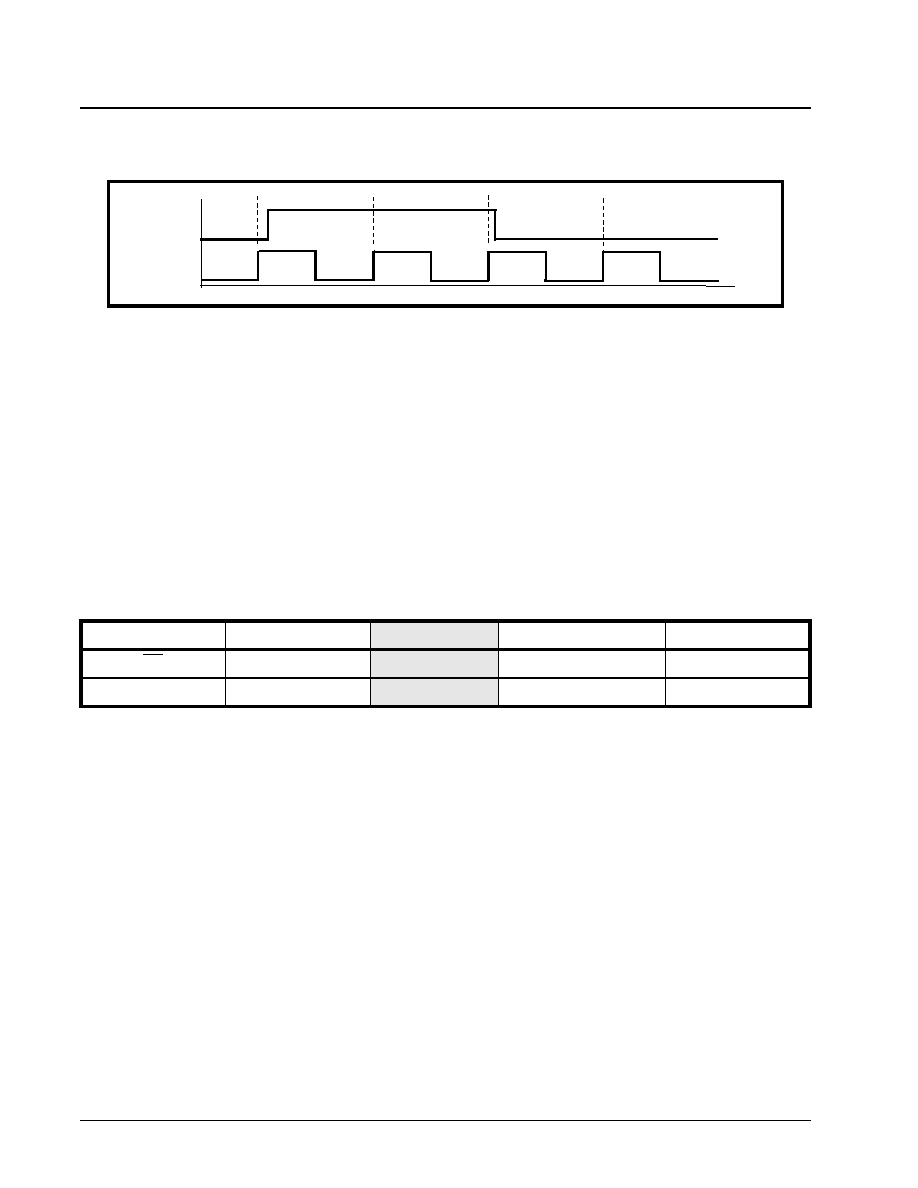
XRT7302
2 CHANNEL E3/DS3/STS-1 LINE INTERFACE UNIT
·Á
·Á
·Á
·Á
PRELIMINARY
REV. 1.1.6
44
N
OTE
: The RNEG(n) output pin is internally tied to Ground
whenever this feature is implemented.
3.8
S
HUTTING
OFF
THE
R
ECEIVE
S
ECTION
The Receiver Section in each channel of the
XRT7302 can be shut off. This feature may be useful
in some redundant system designs. Particularly, in
those designs where the Receive Termination in the
Secondary LIU Line Card has been switched-out and
is not receiving any traffic in parallel with the Primary
Line Card. In this case, it is a waste of power if the
LIU on the Secondary Line Card is consuming the
normal amount of current. This feature can permit
powering down the Receive Section of the LIU's on
the Secondary Line Card which reduces their power
consumption by approximately 80%.
a. Operating in the Hardware Mode
Shut off the Receive Section of Channel(n) by pulling
the RxOFF(n) input pin "High". Turn on the Receive
Section of Channel(n) by pulling the RxOFF(n) input
pin to "Low".
b. Operating in the HOST Mode
Shut off the Receive Section of Channel(n) by writing
a "1" into the RxOFF(n) bit-field in Command Regis-
ter CR3-(n). Turn on the Receive Section of Chan-
nel(n) by writing a "0" into the RxOFF(n) bit-field in
Command Register CR3-(n).
F
IGURE
26. T
HE
BEHAVIOR
OF
THE
RPOS
AND
R
X
C
LK
OUTPUT
SIGNALS
WHILE
THE
XRT7302
IS
TRANSMIT
-
TING
S
INGLE
-R
AIL
DATA
TO
THE
R
ECEIVING
T
ERMINAL
E
QUIPMENT
RxClk
RPOS
COMMAND REGISTER CR3-(N)
D4
D3
D2
D1
D0
SR/(DR)_(n)
LOSMUT(n)
RxOFF(n)
RxClk(n)INV
Reserved
X
X
1
X
X

·Á
·Á
·Á
·Á
2 CHANNEL E3/DS3/STS-1 LINE INTERFACE UNIT
XRT7302
PRELIMINARY
REV. P1.1.6
45
4.0
DIAGNOSTIC FEATURES OF THE XRT7302
The XRT7302 supports equipment diagnostic activi-
ties by supporting the following Loop-Back modes in
each channel in the XRT7302:
∑ Analog Local Loop-Back
∑ Digital Local Loop-Back
∑ Remote Loop-Back
4.1
T
HE
A
NALOG
L
OCAL
L
OOP
-B
ACK
M
ODE
When a given channel in the XRT7302 is configured
to operate in the Analog Local Loop-Back Mode, it ig-
nores any signals that are input to its RTIP(n) and
RRing(n) input pins. The Transmitting Terminal
Equipment transmits clock and data into this channel
via the TPData(n), TNData(n) and TxClk(n) input
pins. This data is processed through the Transmit
Clock Duty Cycle Adjust PLL and the HDB3/B3ZS
Encoder. Finally, this data outputs to the line via the
TTIP(n) and TRing(n) output pins. Additionally, this
data loops back into the Attenuator/Receive Equalizer
Block. This data is processed through the entire Re-
ceive Section of the channel. After this post-Loop-
Back data has been processed through the Receive
Section, it outputs to the Near-End Receiving Termi-
nal Equipment via the RPOS(n), RNEG(n) and Rx-
Clk(n) output pins.
Figure 27 illustrates the path the data takes in a given
channel of the XRT7302 when it is configured to op-
erate in the Analog Local Loop-Back Mode.
A given channel in the XRT7302 can be configured to
operate in the Analog Local Loop-Back Mode by em-
ploying either one of the following two steps:
N
OTE
: See Table 2 for a description of Command Registers
and Addresses for the different channels.
a. Operating in the HOST Mode
To configure Channel (n) to operate in the Analog Lo-
cal Loop-Back Mode, write a "1" into the LLB(n) bit-
field and a "0" into the RLB(n) bit-field in Command
Register CR4.
b. Operating in the Hardware Mode
F
IGURE
27. A
CHANNEL
IN
THE
XRT7302
OPERATING
IN
THE
A
NALOG
L
OCAL
L
OOP
-B
ACK
M
ODE
AGC/
Equalizer
Peak
Detector
LOS Detector
Slicer
Clock
Recovery
Data
Recovery
Invert
Loop MUX
HDB3/
B3ZS
Decoder
LOSTHR(n)
SDI
SDO
SClk
CS
REGR
RTIP(n)
RRing(n)
REQEN(n)
RxClk(n)
RPOS(n)
RNEG(n)
LCV(n)
ENDECDIS
RLOS(n)
LLB(n)
RLB(n)
TAOS(n)
TPData(n)
TNData(n)
TxClk(n)
Notes:
1. (n) = 0 or 1 for respective Channels
2. Serial Processor Interface input pins are shared by the two Channels in HOST Mode and redefined in Hardware Mode.
RLOL(n) EXClk(n)
Device
Monitor
MTIP(n)
MRing(n)
Transmit
Logic
Duty Cycle Adjust
TxLEV(n)
TxOFF(n)
DMO(n)
TTIP(n)
TRing(n)
Pulse
Shaping
HDB3/
B3ZS
Encoder
Serial
Processor
Interface
Analog Local
Loop-Back Path
COMMAND REGISTER CR4-(n)
D4
D3
D2
D1
D0
X
STS-1/DS3_ Ch(n)
E3_ Ch(n)
LLB(n)
RLB(n)
X
X
X
1
0
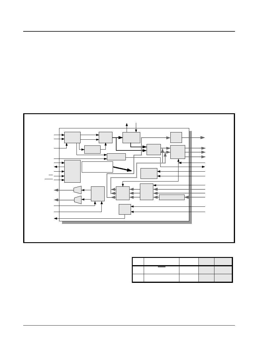
XRT7302
2 CHANNEL E3/DS3/STS-1 LINE INTERFACE UNIT
·Á
·Á
·Á
·Á
PRELIMINARY
REV. P1.1.6
46
To configure Channel (n) to operate in the Analog Lo-
cal Loop-Back Mode, set the LLB(n) input pin "High"
and the RLB(n) input pin "Low".
N
OTE
: The Analog Local Loop-Back mode does not work if
the transmitter is turned off via the TxOFF feature.
4.2
T
HE
D
IGITAL
L
OCAL
L
OOP
-B
ACK
M
ODE
.
When a given channel in the XRT7302 is configured
to operate in the Digital Local Loop-Back Mode, the
channel ignores any signals that are input to the RTIP
and RRing input pins. The Transmitting Terminal
Equipment transmits clock and data into the
XRT7302 via the TPData, TNData and TxClk input
pins. This data is processed through the Transmit
Clock Duty Cycle Adjust PLL and the HDB3/B3ZS
Encoder block. At this point, this data loops back to
the HDB3/B3ZS Decoder block. After this post-Loop-
Back data has been processed through the HDB3/
B3ZS Decoder block, it outputs to the Near-End Re-
ceiving Terminal Equipment via the RPOS, RNEG
and RxClk output pins.
Figure 28 illustrates the path the data takes in the
XRT7302 when the chip is configured to operate in
the Digital Local Loop-Back Mode.
To configure a channel to operate in the Digital Local
Loop-Back Mode, employ either one of the following
two-steps:
a. Operating in the HOST Mode
To configure Channel (n), write a "1" into both the
LLB and RLB bit-fields in Command Register CR4-
(n), as illustrated below.
b. Operating in the Hardware Mode
To configure Channel (n), pull both the LLB input pin
and the RLB input pin "High".
N
OTE
: The Digital Local Loop-Back mode works even if the
transmitter is turned off via the TxOFF feature.
F
IGURE
28. T
HE
D
IGITAL
L
OCAL
L
OOP
-B
ACK
PATH
IN
A
GIVEN
CHANNEL
OF
THE
XRT7302
AGC/
Equalizer
Peak
Detector
LOS Detector
Slicer
Clock
Recovery
Data
Recovery
Invert
Loop MUX
HDB3/
B3ZS
Decoder
LOSTHR(n)
SDI
SDO
SClk
CS
REGR
RTIP(n)
RRing(n)
REQEN(n)
RxClk(n)
RPOS(n)
RNEG(n)
LCV(n)
ENDECDIS
RLOS(n)
LLB(n)
RLB(n)
TAOS(n)
TPData(n)
TNData(n)
TxClk(n)
RLOL(n) EXClk(n)
Device
Monitor
MTIP(n)
MRing(n)
Transmit
Logic
Duty Cycle Adjust
TxLEV(n)
TxOFF(n)
DMO(n)
TTIP(n)
TRing(n)
Pulse
Shaping
HDB3/
B3ZS
Encoder
Serial
Processor
Interface
Digital Local
Loop-Back Path
Notes:
1. (n) = 0 or 1 for respective Channels
2. Serial Processor Interface input pins are shared by the two Channels in HOST Mode and redefined in Hardware Mode.
COMMAND REGISTER CR4-(N)
D4
D3
D2
D1
D0
X
STS-1/DS3_Ch(n) E3_Ch(n) LLB(n)
RLB(n)
X
X
X
1
1

·Á
·Á
·Á
·Á
2 CHANNEL E3/DS3/STS-1 LINE INTERFACE UNIT
XRT7302
PRELIMINARY
REV. P1.1.6
47
4.3
T
HE
R
EMOTE
L
OOP
-B
ACK
M
ODE
When a given channel of the XRT7302 is configured
to operate in the Remote Loop-Back Mode, the chan-
nel ignores any signals that are input to the TPData
and TNData input pins. The channel receives the in-
coming line signal via the RTIP and RRing input pins.
This data is processed through the entire Receive
Section of the channel and outputs to the Receive
Terminal Equipment via the RPOS, RNEG and RxClk
output pins. Additionally, this data is internally looped
back into the Pulse-Shaping block in the Transmit
Section. At this point, this data is routed through the
remainder of the Transmit Section of the channel and
transmitted out onto the line via the TTIP(n) and
TRing(n) output pins.
Figure 29 illustrates the path the data takes in the
XRT7302 when the chip is configured to operate in
the Remote Loop-Back Mode.
To configure a channel to operate in the Remote
Loop-Back Mode employ either one of the following
two steps
a. Operating in the HOST Mode
To configure Channel (n), write a "1" into the RLB bit-
field and a "0" into the LLB bit-field in Command Reg-
ister CR4.
b. Operating in the Hardware Mode
To configure Channel(n), pull both the RLB input pin
to "High" and the LLB input pin to "Low".
4.4
T
X
OFF F
EATURES
The Transmit Section of each Channel in the
XRT7302 can be shut off. When this feature is in-
voked, the Transmit Section of the configured channel
is shut-off and the Transmit Output signals TTIP(n)
and TRing(n) are tri-stated. This feature is useful for
system redundancy conditions or during diagnostic
testing.
a. Operating in the Hardware Mode
Shut off the Channel(n) Transmit Driver by toggling
the TxOFF(n) input pin "High". Turn on the Transmit
Driver by toggling the TxOFF(n) input pin "Low".
b. Operating in the HOST Mode
F
IGURE
29. T
HE
R
EMOTE
L
OOP
-B
ACK
PATH
IN
A
GIVEN
XRT7302 C
HANNEL
AGC/
Equalizer
Peak
Detector
LOS Detector
Slicer
Clock
Recovery
Data
Recovery
Invert
Loop MUX
HDB3/
B3ZS
Decoder
LOSTHR(n)
SDI
SDO
SClk
CS
REGR
RTIP(n)
RRing(n)
REQEN(n)
RxClk(n)
RPOS(n)
RNEG(n)
LCV(n)
ENDECDIS
RLOS(n)
LLB(n)
RLB(n)
TAOS(n)
TPData(n)
TNData(n)
TxClk(n)
RLOL(n) EXClk(n)
Device
Monitor
MTIP(n)
MRing(n)
Transmit
Logic
Duty Cycle Adjust
TxLEV(n)
TxOFF(n)
DMO(n)
TTIP(n)
TRing(n)
Pulse
Shaping
HDB3/
B3ZS
Encoder
Serial
Processor
Interface
Remote
Loop-Back Path
Notes:
1. (n) = 0 or 1 for respective Channels
2. Serial Processor Interface input pins are shared by the two Channels in HOST Mode and redefined in Hardware Mode.
COMMAND REGISTER CR4-(n)
D4
D3
D2
D1
D0
X
STS-1/DS3_Ch(n) E3_Ch(n)
LLB(n)
RLB(n)
X
X
X
0
1
XRT7302
2 CHANNEL E3/DS3/STS-1 LINE INTERFACE UNIT
·Á
·Á
·Á
·Á
PRELIMINARY
REV. P1.1.6
48
Turn off the Channel(n) Transmit Driver by setting the
TxOFF(n) bit-field in Command Register CR1-(n) to
"1".
Writing a "0" into this bit-field enables the Channel(n)
Transmit Driver.
N
OTE
: In order to permit a system designed for redundancy
to quickly shut-off a defective line card and turn-on the
back-up line card, the XRT7302 was designed such that
either Transmitter can quickly be turned-on or turned-off by
toggling the TxOFF(n) input pins. This approach is much
quicker then setting the TxOFF(n) bit-fields via the Micro-
processor Serial Interface.
Table 6 presents a Truth Table which relates the set-
ting of the TxOFF external pin and bit-field for a chan-
nel to the state of the Transmitter. This table applies
to both Channels of the XRT7302.
To control the state of each transmitter via the Micro-
processor Serial interface, connect the TxOFF(n) in-
put pins to GND.
4.5
T
HE
T
RANSMIT
D
RIVE
M
ONITOR
F
EATURES
The Transmit Drive Monitor is used to monitor the line
in the Transmit Direction for the occurrence of fault
conditions such as a short circuit on the line, a defec-
tive Transmit Drive in the XRT7302 or another LIU.
Activate the Channel(n) Transmit Drive Monitor by
connecting the MTIP(n) pin to the TTIP(n) line
through a 270 Ohm resistor connected in series, and
connecting the MRing(n) pin to the TRing(n) line
through a 270 Ohm resistor connected in series.
Such an approach is illustrated in Figure 30.
COMMAND REGISTER CR1-(n)
D4
D3
D2
D1
D0
TxOFF(n) TAOS(n)
TxClkINV(n)
TxLEV(n) TxBIN(n)
1
X
X
X
X
T
ABLE
6: T
HE
R
ELATIONSHIP
B
ETWEEN
THE
T
X
OFF I
NPUT
P
IN
,
THE
T
X
OFF B
IT
F
IELD
AND
THE
S
TATE
OF
THE
T
RANSMITTER
S
TATE
OF
THE
T
X
OFF
I
NPUT
P
IN
S
TATE
OF
THE
T
X
OFF
B
IT
F
IELD
S
TATE
OF
THE
T
RANSMITTER
LOW
0
ON (Transmitter is Active)
LOW
1
OFF (Transmitter is Tri-Stated)
HIGH
0
OFF (Transmitter is Tri-Stated)
HIGH
1
OFF (Transmitter is Tri-Stated)
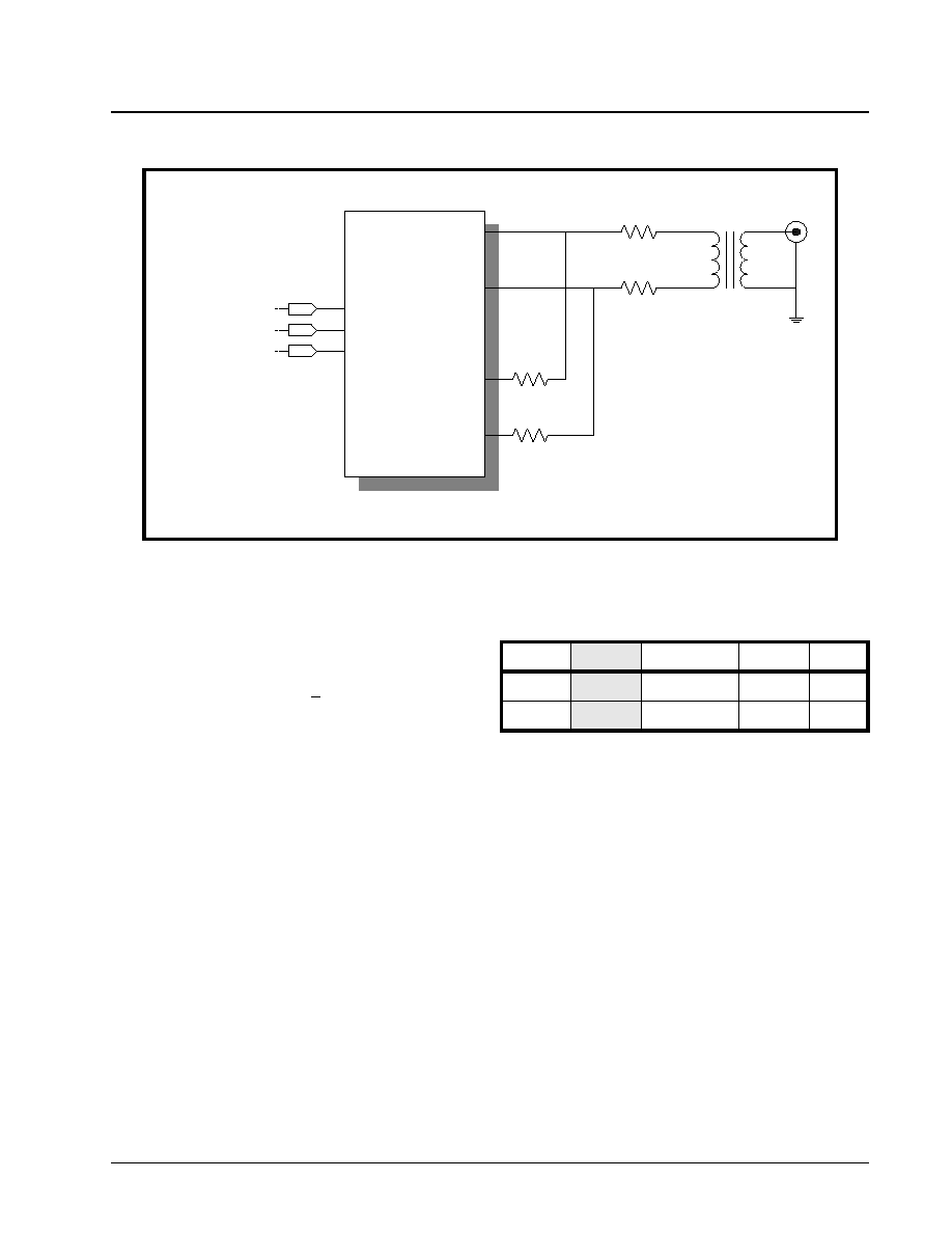
·Á
·Á
·Á
·Á
2 CHANNEL E3/DS3/STS-1 LINE INTERFACE UNIT
XRT7302
PRELIMINARY
REV. P1.1.6
49
When the Transmit Drive Monitor circuitry in a given
line is connected to the line as illustrated in Figure 30,
then it monitors the line for transitions. As long as the
Transmit Drive Monitor circuitry detects transitions on
the line via the MTIP(n) and MRing(n) pins, it keeps
the DMO (Drive Monitor Output) signal "Low". How-
ever, if the Transmit Drive Monitor circuit detects no
transitions on the line for 128+32 TxClk periods, the
DMO (Drive Monitor Output) signal toggles "High".
N
OTE
: The Transmit Drive Monitor circuit does not have to
be used to operate the Transmit Section of the XRT7302.
This is purely a diagnostic feature.
4.6
T
HE
TAOS (T
RANSMIT
A
LL
O
NE
S) F
EATURE
The XRT7302 can command any channel to transmit
an all "1's" pattern onto the line by toggling a single
input pin or by setting a single bit-field in one of the
Command Registers to "1".
N
OTE
: When this feature is activated, the Transmit Section
of the configured channel in the XRT7302 overwrites the
Terminal Equipment data with an all "1's" pattern.
a. Operating in the Hardware Mode
Configure Channel(n) to transmit an all "1's" pattern
by toggling the TAOS(n) input pin "High". Terminate
the all "1's" pattern by toggling the TAOS(n) input pin
"Low".
b. Operating in the HOST Mode
Configure Channel(n) to transmit an all "1's" pattern
by writing to Command Register CR1-(n) and setting
the TAOS(n) bit-field (D3) to "1".
Terminate the all "1's" pattern by writing to Command
Register CR1-(n) and setting the TAOS(n) bit-field
(D3) to "0".
5.0
THE MICROPROCESSOR SERIAL INTER-
FACE
The on-chip Command Registers of XRT7302 DS3/
E3/STS-1 Line Interface Unit IC are used to configure
the XRT7302 into a wide-variety of modes. This sec-
tion discusses the following:
1. The description of the Command Registers.
2. A description on how to use the Microprocessor
Serial Interface.
5.1
D
ESCRIPTION
OF
THE
C
OMMAND
R
EGISTERS
Table 7 lists the Command Registers, their Addresses
and their bit-formats.
F
IGURE
30. T
HE
XRT7302
EMPLOYING
THE
T
RANSMIT
D
RIVE
M
ONITOR
F
EATURES
R1 = 31.6
R2 = 31.6
Channel (n)
T x P O S ( n )
T x N E G ( n )
TxLineClk(n)
TTIP(n)
TRing(n)
TPData(n)
TNData(n)
TxClk(n)
O n l y O n e C h a n n e l S h o w n
1:1
J 1
B N C
MTIP(n)
MRing(n)
R3 = 270
R4 = 270
COMMAND REGISTER CR1-(N)
D4
D3
D2
D1
D0
TxOFF(n) TAOS(n)
TxClkINV(n)
TxLEV(n) TxBIN(n)
0
1
X
X
X

XRT7302
2 CHANNEL E3/DS3/STS-1 LINE INTERFACE UNIT
·Á
·Á
·Á
·Á
PRELIMINARY
REV. P1.1.6
50
Address
The register addresses are presented in the Hexa-
decimal format.
Type:
The Command Registers are either Read-Only (RO)
or Read/Write (R/W) registers. Each channel of the
XRT7302 has eight command registers, CR0-(n)
through CR7-(n) where (n) = 0 or 1. The associated
addresses for each channel is presented in Table 7.
N
OTE
: The default value for each of the bit-fields in these
registers is "0".
5.2
D
ESCRIPTION
OF
B
IT
-F
IELDS
FOR
EACH
C
OM
-
MAND
R
EGISTER
5.2.1
Command Register - CR0-(n)
The bit-format and default values for Command Reg-
ister CR0-(n) are listed below followed by the function
of these bit-fields.
Bit D4 - RLOL(n) (Receive Loss of Lock Status -
Channel(n))
This Read-Only bit-field reflects the lock status of the
Channel(n) Clock Recovery Phase-Locked-Loop in
the XRT7302.
This bit-field is set to "0" if the Clock Recovery PLL is
in lock with the incoming line signal. This bit-field is
T
ABLE
7: A
DDRESSES
AND
B
IT
F
ORMATS
OF
XRT7302 C
OMMAND
R
EGISTERS
R
EGISTER
B
IT
-F
ORMAT
ADDRESS
COMMAND
REGISTER
TYPE
D4
D3
D2
D1
D0
C
HANNEL
0
0x00
CR0-0
RO
RLOL0
RLOS0
ALOS0
DLOS0
DMO0
0x01
CR1-0
R/W
TxOFF0
TAOS0
TxClkINV0
TxLEV0
TxBIN0
0x02
CR2-0
R/W
Reserved
ENDECDIS0
ALOSDIS0
DLOSDIS0
REQEN0
0x03
CR3-0
R/W
SR/DR_0
LOSMUT0
RxOFF0
RxClk0INV
Reserved
0x04
CR4-0
R/W
Reserved
STS-1/DS3_Ch0
E3_CH0
LLB0
RLB0
0x05
CR5-0
R/W
Reserved
Reserved
Reserved
Reserved
Reserved
0x06
CR6-0
R/W
Reserved
Reserved
Reserved
Reserved
Reserved
0x07
CR7-0
R/W
Reserved
Reserved
Reserved
Reserved
Reserved
C
HANNEL
1
0x08
CR0-1
RO
RLOL1
RLOS1
ALOS1
DLOS1
DMO1
0x09
CR1-1
R/W
TxOFF1
TAOS1
TxClkINV1
TxLEV1
TxBIN1
0x0A
CR2-1
R/W
Reserved
ENDECDIS1
ALOSDIS1
DLOSDIS1
REQEN1
0x0B
CR3-1
R/W
SR/DR_1
LOSMUT1
RxOFF1
RxClk1INV
Reserved
0x0C
CR4-1
R/W
Reserved
STS-1/DS3_Ch1
E3_CH1
LLB1
RLB1
0x0D
CR5-1
R/W
Reserved
Reserved
Reserved
Reserved
Reserved
0x0E
CR6-1
R/W
Reserved
Reserved
Reserved
Reserved
Reserved
0x0F
CR7-1
R/W
Reserved
Reserved
Reserved
Reserved
Reserved
COMMAND REGISTER CR0-(N)
D4
D3
D2
D1
D0
RLOL
RLOS
ALOS
DLOS
DMO
1
1
1
1
1

·Á
·Á
·Á
·Á
2 CHANNEL E3/DS3/STS-1 LINE INTERFACE UNIT
XRT7302
PRELIMINARY
REV. P1.1.6
51
set to "1" if the Clock Recovery PLL is out of lock with
the incoming line signal.
Bit D3 - RLOS(n) (Receive Loss of Signal Status -
Channel(n))
This Read-Only bit-field indicates whether or not
Channel(n) of the Receiver is currently declaring an
LOS (Loss of Signal) Condition.
This bit-field is set to "0" if Channel(n) is NOT current-
ly declaring the LOS Condition or, this bit-field is set
to "1" if Channel(n) is declaring an LOS Condition.
Bit D2 - ALOS(n) (Analog Loss of Signal Status -
Channel(n))
This Read-Only bit-field indicates whether or not the
Channel(n) Analog LOS Detector is currently declar-
ing an LOS condition.
This bit-field is set to "0" if the Analog LOS Detector is
NOT currently declaring an LOS condition. This bit-
field is set to "1" if the Analog LOS Detector is cur-
rently declaring an LOS condition.
N
OTE
: The purpose is to isolate the Detector (e.g., either
the Analog LOS or the Digital LOS detector) that is declar-
ing the LOS condition. This feature may be useful for trou-
bleshooting/debugging purposes.
Bit D1 - DLOS(n) (Digital Loss of Signal Status -
Channel(n))
This Read-Only bit-field indicates whether or not the
Channel(n) Digital LOS Detector is currently declar-
ing an LOS condition.
This bit-field is set to "0" if the Digital LOS Detector is
NOT currently declaring an LOS condition. This bit-
field is set to "1" if the Digital LOS Detector is current-
ly declaring an LOS condition.
N
OTE
: The purpose is to isolate the Detector (e.g., either
the Analog LOS or the Digital LOS detector) that is declar-
ing the LOS condition. This feature may be useful for trou-
bleshooting/debugging purposes.
Bit D0 - DMO(n) (Drive Monitor Output Status -
Channel(n))
This Read-Only bit-field reflects the status of the
DMO output pin.
5.2.2
Command Register CR1
The bit-format and default values for Command Reg-
ister CR1-(n) are listed below followed by the function
of these bit-fields.
Bit D4 - TxOFF(n) (Transmitter OFF - Channel(n))
This Read/Write bit-field is used to turn off the Chan-
nel(n) Transmitter.
Writing a "1" to this bit field turns off the Transmitter
and tri-state the Transmit Output. Writing a "0" to this
bit-field turns on the Transmitter.
Bit D3 - TAOS(n) (Transmit All OneS - Channel(n))
This Read/Write bit-field is used to command the
Channel(n) Transmitter to generate and transmit an
all "1's" pattern onto the line.
Writing a "1" to this bit-field commands the Transmit-
ter to transmit an all "1's" pattern onto the line. Writ-
ing a "0" to this bit-field commands normal operation.
Bit D2 - TxClkINV(n) (Transmit Clock Invert -
Channel(n))
This Read/Write bit-field is used to configure the
Transmitter in the XRT7302 to sample the signal at
the TPData and TNData pins on the rising edge or
falling edge of TxClk (the Transmit Line Clock signal).
Writing a "1" to this bit-field configures the Transmitter
to sample the TPData and TNData input pins on the
rising edge of TxClk. Writing a "0" to this bit-field con-
figures the Transmitter to sample the TPData and
TNData input pins on the falling edge of TxClk.
Bit D1 - TxLEV(n) (Transmit Line Build-Out En-
able/Disable Select - Channel(n))
This Read/Write bit-field is used to enable or disable
the Channel(n) Transmit Line Build-Out circuit in the
XRT7302.
Setting this bit-field "High" disables the Channel(n)
Line Build-Out circuit. In this mode, Channel(n) out-
puts partially-shaped pulses onto the line via the
TTIP(n) and TRing(n) output pins.
Setting this bit-field "Low" enables the Channel(n)
Line Build-Out circuit. In this mode, Channel(n) out-
puts shaped pulses onto the line via the TTIP(n) and
TRing(n) output pins.
In order to comply with the Isolated DSX-3/STSX-1
Pulse Template Requirements (per Bellcore GR-499-
CORE or GR-253-CORE):
a. Set this bit-field to "1" if the cable length between
the Cross-Connect and the transmit output of Chan-
nel(n) is greater than 225 feet.
b. Set this bit-field to "0" if the cable length between
the Cross-Connect and the transmit output of Chan-
nel(n) is less than 225 feet.
N
OTE
: This bit-field is active only if the XRT7302 is config-
ured to operate in the DS3 or SONET STS-1 Modes.
COMMAND REGISTER CR1-(N)
D4
D3
D2
D1
D0
TxOFF(n) TAOS(n)
TxClkINV(n)
TxLEV(n) TxBIN(n)
0
0
0
0
0

XRT7302
2 CHANNEL E3/DS3/STS-1 LINE INTERFACE UNIT
·Á
·Á
·Á
·Á
PRELIMINARY
REV. P1.1.6
52
If the cable length is greater than 225 feet, set this bit-
field to "1" in order to increase the amplitude of the
Transmit Output Signal. If the cable length is less
than 225 feet, set this bit-field to "0".
N
OTE
: This option is only available when the XRT7302 is
operating in the DS3 or STS-1 Mode.
Bit D0 - TxBIN(n) (Transmit Binary Data - Chan-
nel(n))
This Read/Write bit-field is used to configure the
Channel(n) Transmitter to accept an un-encoded bi-
nary data stream via the TPData input and convert
this data into the appropriate bipolar signal for the
line.
Writing a "1" configures the Transmitter to accept a bi-
nary data stream via the TPData input. The TNData
input is ignored.
This form of data acceptance is sometimes referred
to as Single-Rail mode operation. The Transmitter
then encodes this data into the appropriate line code
(e.g., B3ZS or HDB3) prior to its transmission over
the line.
Writing a "0" configures the Transmitter to accept da-
ta in a Dual-Rail manner via TPData and TNData in-
puts.
5.2.3
Command Register CR2-(n)
The bit-format and default values for Command Reg-
ister CR2-(n) are listed below followed by the function
of each of these bit-fields.
Bit D4 - Reserved
Bit D3 - ENDECDIS (B3ZS/HDB3 Encoder/Decod-
er-Disable - Channel(n))
This Read/Write bit-field is used to enable or disable
the Channel(n) B3ZS/HDB3 Encoder and Decoder
blocks.
Writing a "1" to this bit-field disables the B3ZS/HDB3
Encoder and Decoder blocks. Writing a "0" to this bit-
field enables the B3ZS/HDB3 Encoder and Decoder
blocks.
N
OTE
: This Encoder/Decoder performs HDB3 Encoding/
Decoding if the XRT7302 is operating in the E3 Mode. Oth-
erwise, it performs B3ZS Encoding/Decoding.
Bit D2 - ALOSDIS (Analog LOS Disable - Chan-
nel(n))
This Read/Write bit-field is used to enable or disable
the Channel(n) Analog LOS Detector.
Writing a "0" to this bit-field enables the Analog LOS
Detector. Writing a "1" to this bit-field disables the
Analog LOS Detector.
N
OTE
: If the Analog LOS Detector is disabled, then the
RLOS input pin is only asserted by the DLOS (Digital LOS
Detector).
Bit D1 - DLOSDIS (Digital LOS Disable - Chan-
nel(n))
This Read/Write bit-field to used to enable or disable
the Channel(n) Digital LOS Detector .
Writing a "0" to this bit-field enables the Digital LOS
Detector. Writing a "1" to this bit-field disables the
Digital LOS Detector.
N
OTE
: If the Digital LOS Detector is disabled, then the
RLOS input pin is only asserted by the ALOS (Analog LOS
Detector).
Bit D0 - REQEN (Receive Equalization Enable -
Channel(n))
This Read/Write bit-field is used to either enable or
disable the Channel(n) internal Receive Equalizer of
the XRT7302.
Writing a "1" to this bit-field enables the Internal
Equalizer. Writing a "0" to this bit-field disables the
Internal Equalizer.
5.2.4
Command Register CR3-(n)
The bit-format and default values for Command Reg-
ister CR3 are listed below followed by the function of
these bit-fields.
Bit D4 - SR/DR_(n)(Single-Rail/Dual-Rail Data Out-
put - Channel(n))
This Read/Write bit-field is used to configure Chan-
nel(n) in the XRT7302 to output the received data
from the Remote Terminal in a binary or Dual-Rail for-
mat.
Writing a "1" to this bit-field configures Channel(n) to
output data to the Terminal Equipment in a binary
Single-Rail format via the RPOS(n) output pin.
RNEG(n) is grounded. Writing a "0" to this bit-field
configures Channel(n) to output data to the Terminal
Equipment in a Dual-Rail format via both the
RPOS(n) and RNEG(n) output pins.
COMMAND REGISTER CR2-(N)
D4
D3
D2
D1
D0
Reserved ENDECDIS ALOSDIS
DLOSDIS
REQEN
X
0
0
0
0
COMMAND REGISTER CR3-(N)
D4
D3
D2
D1
D0
SR/DR_(n) LOSMUT(n) RxOFF(n) RxClk(n)INV Reserved
0
1
0
0
0

·Á
·Á
·Á
·Á
2 CHANNEL E3/DS3/STS-1 LINE INTERFACE UNIT
XRT7302
PRELIMINARY
REV. P1.1.6
53
Bit D3 - LOSMUT(n) (Recovered Data MUTing dur-
ing LOS Condition - Channel(n))
This Read/Write bit-field is used to configure Chan-
nel(n) in the XRT7302 to NOT output any recovered
data from the line while it is declaring an LOS condi-
tion.
Writing a "0" to this bit-field configures the chip to out-
put recovered data even while the XRT7302 is declar-
ing an LOS condition. Writing a "1" to this bit-field
configures the chip to NOT output the recovered data
while an LOS condition is being declared.
N
OTE
: In this mode, RPOS(n) and RNEG(n) is set to "0"
asynchronously.
Bit D2 - RxOFF(n) (Receive Section - Shut OFF Se-
lect)
This Read/Write bit-field is used to shut-off the Re-
ceive Section of Channel(n) in the XRT7302. The
purpose of this feature is to permit conservation of
power consumption when this is the back-up device
in a Redundancy System.
Writing a "1" into this bit-field shuts off the Receive
Section of Channel(n). Writing a "0" into this bit-field
turns on the Receive Section of Channel(n).
Bit D1 - RxClk(n)INV (Invert RxClk(n))
This Read/Write bit-field is used to configure the Re-
ceiver of Channel(n) of the XRT7302) to output the
recovered data on either the rising edge or the falling
edge of the RxClk(n) clock signal.
Writing a "0" to this bit-field configures the Receiver to
output the recovered data on the rising edge of the
RxClk(n) output signal. Writing a "1" to this bit-field
configures the Receiver to output the recovered data
on the falling edge of the RxClk(n) output signal.
Bit D0 - Reserved
This bit-field has no defined functionality.
Command Register CR4-(n)
The bit-format and default values for Command Reg-
ister CR4 are listed below followed by the function of
each of these bit fields.
Bit D4 - Reserved
This bit-field has no defined functionality.
COMMAND REGISTER CR4-(N)
D4
D3
D2
D1
D0
Reserved STS-1/DS3_ Ch(n) E3_Ch(n) LLB(n) RLB(n)
0
0
0
0
0

XRT7302
2 CHANNEL E3/DS3/STS-1 LINE INTERFACE UNIT
·Á
·Á
·Á
·Á
PRELIMINARY
REV. P1.1.6
54
Bit D3 - STS-1/(DS3_(n)) - Channel(n) - Mode Se-
lect
This Read/Write bit field is used to configure Chan-
nel(n) to operate in either the SONET STS-1 Mode or
the DS3 Mode.
Writing a "0" into this bit-field configures Channel(n)
to operate in the DS3 Mode. Writing a "1" into this
bit-field configures Channel(n) to operate in the SO-
NET STS-1 Mode.
N
OTE
: This bit-field is ignored if the E3_Ch(n) bit-field (e.g.,
D2 in this Command Register) is set to "1".
Bit D2 - E3 Mode Select - Channel(n)
This Read/Write bit-field is used to configure Chan-
nel(n) to operate in the E3 Mode.
Writing a "0" into this bit-field configures Channel(n)
to operate in either the DS3 or SONET STS-1 Mode
as specified by the setting of the DS3 bit-field in this
Command Register. Writing a "1" into this bit-field
configures Channel(n) to operate in the E3 Mode.
Bit D1 - LLB(n) (Local Loop-Back - Channel(n))
This Read/Write bit-field along with RLB(n) is used to
configure Channel(n) to operate in any one of a vari-
ety of Loop-Back modes.
Table 8 relates the contents of LLB(n) and RLB(n)
and the corresponding Loop-Back mode for Chan-
nel(n).
Bit D0 - RLB(n) (Remote Loop-Back - Channel(n))
This Read/Write bit-field along with LLB(n) is used to
configure Channel(n) to operate in any one of a vari-
ety of Loop-Back modes.
Table 8 relates the contents of LLB(n) and RLB(n)
and the corresponding Loop-Back mode for Chan-
nel(n).
5.3
O
PERATING
THE
M
ICROPROCESSOR
S
ERIAL
I
NTERFACE
.
The XRT7302 Serial Interface is a simple four wire in-
terface that is compatible with many of the micro-con-
trollers available in the market. This interface con-
sists of the following signals:
∑ CS - Chip Select (Active Low)
∑ SClk - Serial Clock
∑ SDI - Serial Data Input
∑ SDO - Serial Data Output
Using the Microprocessor Serial Interface
The following instructions for using the Microproces-
sor Serial Interface are best understood by referring
to the diagram in Figure 31 and the timing diagram in
Figure 32.
In order to use the Microprocessor Serial Interface, a
clock signal must be first applied to the SClk input pin.
Then, initiate a Read or Write operation by asserting
the active-low Chip Select input pin CS. It is impor-
tant to assert the CS pin (e.g., toggle it "Low") at least
50ns prior to the very first rising edge of the clock sig-
nal.
Once the CS input pin has been asserted, the type of
operation and the target register address must now
be specified. Provide this information to the Micro-
processor Serial Interface by writing eight serial bits
of data into the SDI input.
N
OTE
: Each of these bits is clocked into the SDI input on
the rising edge of SClk.
Bit 1- R/W (Read/Write) Bit
This bit is clocked into the SDI input on the first rising
edge of SClk after CS has been asserted. This bit in-
dicates whether the current operation is a Read or
Write operation. A "1" in this bit specifies a Read op-
eration, a "0" in this bit specifies a Write operation.
Bits 2 through 5: The four (4) bit Address Values
(labeled A0, A1, A2 and A3)
The next four rising edges of the SClk signal clocks in
the 4-bit address value for this particular Read or
Write operation. The address selects the Command
Register in the XRT7302 that the user either be read-
ing data from or writing data to. The address bits
must be applied to the SDI input pin in ascending or-
der with the LSB (least significant bit) first.
Bit 6 and 7:
T
ABLE
8: C
ONTENTS
OF
LLB(
N
)
AND
RLB(
N
)
AND
THE
C
ORRESPONDING
L
OOP
-B
ACK
M
ODE
FOR
C
HANNEL
(
N
)
LLB
(n)
RLB
(n)
L
OOP
-B
ACK
M
ODE
(
FOR
C
HANNEL
(n)
)
0
0
None
1
0
Analog Loop-Back Mode (See Section 4.1 for Details)
1
1
Digital Loop-Back Mode (See Section 4.2 for Details
0
1
Remote Loop-Back Mode (See Section 4.3 for Details

·Á
·Á
·Á
·Á
2 CHANNEL E3/DS3/STS-1 LINE INTERFACE UNIT
XRT7302
PRELIMINARY
REV. P1.1.6
55
A4 and A5 must be set to "0" as shown in Figure 31.
Bit 8 - A6:
The value of "A6" is a don't care.
Once these first 8 bits have been written into the Mi-
croprocessor Serial Interface, the subsequent action
depends upon whether the current operation is a
Read or Write operation.
Read Operation
Once the last address bit (A3) has been clocked into
the SDI input, the Read operation proceeds through
an idle period lasting three SClk periods. On the fall-
ing edge of SClk Cycle #8 (see Figure 31) the serial
data output signal (SDO) becomes active. At this
point, reading the data contents of the addressed
Command Register at Address [A3, A2, A1, A0] via
the SDO output pin can begin. The Microprocessor
Serial Interface outputs this five bit data word (D0
through D4) in ascending order with the LSB first, on
the falling edges of the SClk pin. Consequently, the
data on the SDO output pin is sufficiently stable for
reading by the Microprocessor on the very next rising
edge of the SClk pin.
Write Operation
Once the last address bit (A3) has been clocked into
the SDI input, the Write operation proceeds through
an idle period lasting three SClk periods. Prior to the
rising edge of SClk Cycle # 9 (see Figure 31). Apply
the desired eight bit data word to the SDI input pin via
the Microprocessor Serial Interface. The Micropro-
cessor Serial Interface latches the value on the SDI
input pin on the rising edge of SClk. Apply this word
(D0 through D7) serially, in ascending order with the
LSB first.
Simplified Interface Option
The design of the circuitry connecting to the Micro-
processor Serial Interface can be simplified by tying
both the SDO and SDI pins together and reading data
from and/or writing data to this combined signal. This
simplification is possible because only one of these
signals are active at any given time. The inactive sig-
nal is tri-stated.
N
OTES
:
1. A4 and A5 is always "0"
2. R/W = "1" for "Read" Operations
3. R/W = "0" for "Write" Operations
4. Shaded blocks denotes a "don't care" value
F
IGURE
31. M
ICROPROCESSOR
S
ERIAL
I
NTERFACE
D
ATA
S
TRUCTURE
D0
D1
D2
0
0
0
D4
D3
High Z
SDO
A0
D0
R/W
D1
A6
0
0
A3
A2
A1
D7
D6
D5
D4
D3
D2
SDI
1
2
3
4
5
6
7
8
9
10
11
12
13
14
15
16
SClk
CS
High Z

XRT7302
2 CHANNEL E3/DS3/STS-1 LINE INTERFACE UNIT
·Á
·Á
·Á
·Á
PRELIMINARY
REV. P1.1.6
56
F
IGURE
32. T
IMING
D
IAGRAM
FOR
THE
M
ICROPROCESSOR
S
ERIAL
I
NTERFACE
SDI
R/W
A1
A0
CS
SClk
CS
SClk
SDI
SDO
D0
D1
D2
D7
t22
t21
t23
t24
t25
t26
t27
t28
t29
t30
t31
t32
t33
Hi-Z
Hi-Z
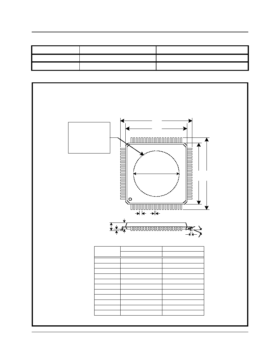
·Á
·Á
·Á
·Á
2 CHANNEL E3/DS3/STS-1 LINE INTERFACE UNIT
XRT7302
REV. 1.1.6
57
ORDERING INFORMATION
PACKAGE DIMENSIONS
P
ART
#
P
ACKAGE
O
PERATING
TEMPERATURE
R
ANGE
XRT7302IV
80 Pin Thermally Enhanced TQFP
-40
o
C to +85
o
C
T
HERMAL
I
NFORMATION
Theta - J
A
= 23∞ C/W
Theta J
C
= 5.32∞ C/W
Heat Slug
Pure Copper
OFHC 0.9999
Solder Plated
(package bottom)
80 LEAD THIN QUAD FLAT PACK
WITH Cu HEAT SLUG
(14X14X1.4mm, TQFP)
Rev. 1.0
D
D
1
D
1
D
A
2
A
1
A
e
B
C
L
1
20
21
40
80
61
60
41
S Y M B O L
1.40 1.60
0.055 0.063
A
0.05 0.15
0.002 0.006
A
1
1.35 1.45
0.053 0.057
A
2
8.64 9.40
0.340 0.370
0
o
7
o
0
o
7
o
0.45 0.75
0.018 0.030
L
0 . 6 5 B S C
0 . 0 2 5 6 B S C
e
13.90 14.10
0.547 0.555
D
1
15.80 16.20
0.622 0.638
D
0.09 0.20
0.004 0.008
C
0.22 0.38
0.009 0.015
B
MIN MAX
MIN MAX
I N C H E S
M I L L I M E T E R S
Note: the control dimension is the millimeter column

·Á
·Á
·Á
·Á
XRT7302
2 CHANNEL E3/DS3/STS-1 LINE INTERFACE UNIT
REV. 1.1.6
58
NOTICE
EXAR Corporation reserves the right to make changes to the products contained in this publication in order
to improve design, performance or reliability. EXAR Corporation assumes no responsibility for the use of
any circuits described herein, conveys no license under any patent or other right, and makes no represen-
tation that the circuits are free of patent infringement. Charts and schedules contained here in are only for
illustration purposes and may vary depending upon a user's specific application. While the information in
this publication has been carefully checked; no responsibility, however, is assumed for inaccuracies.
EXAR Corporation does not recommend the use of any of its products in life support applications where
the failure or malfunction of the product can reasonably be expected to cause failure of the life support sys-
tem or to significantly affect its safety or effectiveness. Products are not authorized for use in such applica-
tions unless EXAR Corporation receives, in writing, assurances to its satisfaction that: (a) the risk of injury
or damage has been minimized; (b) the user assumes all such risks; (c) potential liability of EXAR Corpo-
ration is adequately protected under the circumstances.
Copyright 2000 EXAR Corporation
Datasheet September 2000
Reproduction, in part or whole, without the prior written consent of EXAR Corporation is prohibited.
REVISION HISTORY
Rev. 1.0.1: Pin naming conventions standardized with use of uppercase and lowercase letters. Modified
and added title to Pin Out diagram for readability.
The pin descriptions for pins 30 ("REQ_EN1"), 31 ("REQ_EN2"), 61 ("TxOFF2"), 80 ("TxOFF1") have been
revised. Added Table 7.
Rev. 1.0.2: Added Absolute Maximum Ratings and Test Conditions. Book marked PDF file.
Rev. 1.0.3: Minor formatting changes for readability
Rev. 1.1.0: Standardize pin names, updated block diagram, updated Electrical Characteristics, minor
grammar edits, removed "Preliminary".
Rev. 1.1.1: Pin 7 - Receive Analog VDD to Receive Digital VDD and pin 56 - Transmit Digital GND instead
of Receive. Nomenclature for GND and VDD changed to include A-for analog, and D-for Digital. Package
designation from IQ to IV.
Rev. 1.1.2: Added Tx Control title in block diagram.
Rev. 1.1.3: Modified package dimensions drawing adding Heat Slug integral to package bottom.
Rev. 1.1.4: Modified figures 3 & 4
Rev. 1.1.5: Modified figure 4, LCV signal
Rev. 1.1.6: Modified both channels where n= 1 or 2 to n= 0 or 1. Revised grammar. Changed RxIN to RTIP/
RRING in figure 21.