 | ÐлекÑÑоннÑй компоненÑ: XRT73L02A | СкаÑаÑÑ:  PDF PDF  ZIP ZIP |
/home/web/doc/html/exar/208058
Exar
Coporation 48720 Kato Road, Fremont CA, 94538
·
(510) 668-7000
·
FAX (510) 668-7200
·
www.exar.com
áç
áç
áç
áç
PRELIMINARY
XRT73L02A
2 CHANNEL E3/DS3/STS-1 LINE INTERFACE UNIT
NOVEMBER 2001
REV. 2.0.0
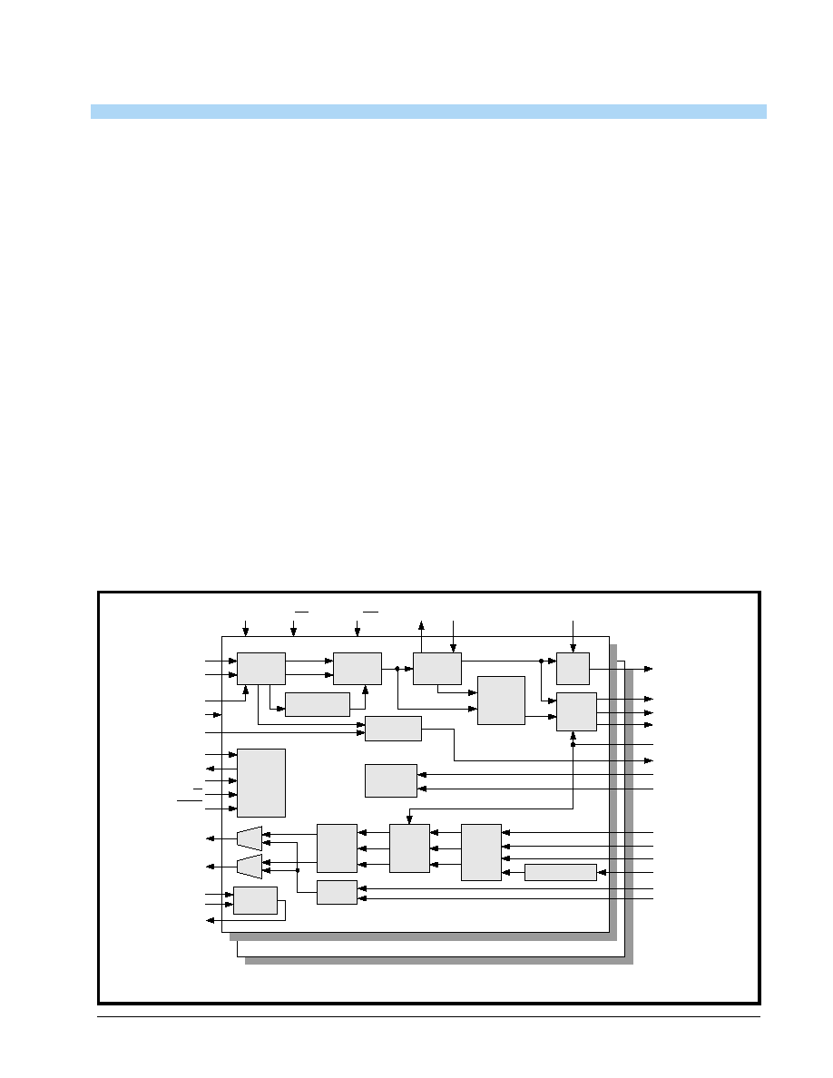
GENERAL DESCRIPTION
The XRT73L02A Dual Channel E3/DS3/STS-1 Trans-
ceiver is an improved version of the XRT73L02 and
consists of two fully integrated transmitter and receiv-
er line transceivers designed for E3, DS3 or SONET
STS-1 applications.
Each channel can be configured to support the E3
(34.368 Mbps), DS3 (44.736 Mbps) or the SONET
STS-1 (51.84 Mbps) rates. Each channel can be con-
figured to operate in a mode/data rate that is indepen-
dent of the other channel.
In the transmit direction, each channel in the
XRT73L02A encodes input data to either B3ZS or
HDB3 format and converts the data into the appropri-
ate pulse shapes for transmission over coaxial cable
via a 1:1 transformer.
In the receive direction, the XRT73L02A can perform
Equalization on incoming signals, perform Clock Re-
covery, decode data from either B3ZS or HDB3 for-
mat, convert the receive data into TTL/CMOS format,
check for LOS or LOL conditions and detect and de-
clare the occurrence of Line Code Violations.
FEATURES
· Incorporates an improved Timing Recovery circuit
and is pin and functional compatible to XRT73L02
· Meets E3/DS3/STS-1 Jitter Tolerance Require-
ments
· Contains a 4-Wire Microprocessor Serial Interface
· Full Loop-back Capability
· Transmit and Receive Power Down Modes
· Full Redundancy Support
· Single +3.3V Power Supply
· Uses Minimum External components
· Operates over -40°C to +85°C Temperature Range
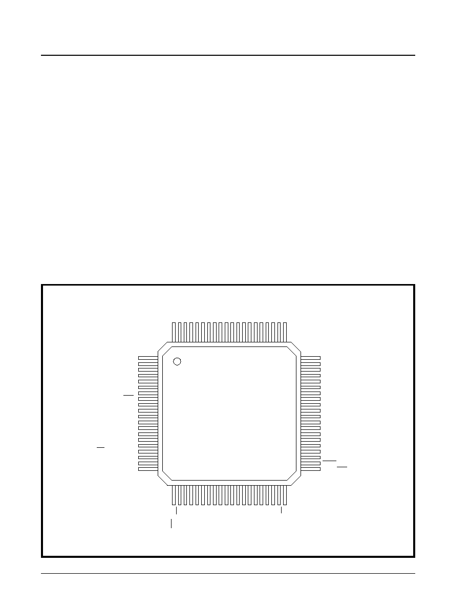
· Available in an 80 pin TQFP package
APPLICATIONS
· Digital Cross Connect Systems
· CSU/DSU Equipment
· Routers
· Fiber Optic Terminals
· Multiplexers
· ATM Switches
XRT73L02A BLOCK DIAGRAM
AGC/
Equalizer
Serial
Processor
Interface
Peak Detector
LOS Detector
Pulse
Shaping
HDB3/
B3ZS
Encoder
Transmit
Logic
Duty Cycle Adjust
Slicer
Clock
Recovery
Data
Recovery
Invert
Loop MUX
HDB3/
B3ZS
Decoder
SDI
SDO
SClk
CS
REGR
TTIP_(n)
TRing_(n)
RTIP_(n)
RRing_(n)
REQEN_(n)
RxClk_(n)
RPOS_(n)
RNEG_(n)
LCV_(n)
RLOS_(n)
LLB_(n)
RLB_(n)
TAOS_(n)
TPData_(n)
TNData_(n)
TxClk_(n)
E3_Ch_(n) STS-1/DS3_Ch_(n) Host/HW RLOL_(n) ExClk_(n) RxClkINV
Channel 0
Channel 1
Device
Monitor
Tx
Control
TxLEV_(n)
TxOFF_(n)
DMO_(n)
MTIP_(n)
MRing_(n)
ENDECDIS
Notes: 1. (n) = 0 or 1 for the respective channel.
2. Serial Processor Interface pins are shared by both Channels in HOST Mode and are redefined in Hardware Mode.
LOSTHR_(n)
RxOFF_(n)
XRT73L02A
áç
áç
áç
áç
2 CHANNEL E3/DS3/STS-1 LINE INTERFACE UNIT
REV. 2.0.0
PRELIMINARY
2
TRANSMIT INTERFACE CHARACTERISTICS
· Accepts either Single-Rail or Dual-Rail data from
Terminal Equipment and generates a bipolar signal
· Integrated Pulse Shaping Circuit
· Built-in B3ZS/HDB3 Encoder (which can be dis-
abled)
· Contains Transmit Clock Duty Cycle Correction Cir-
cuit on-chip
· Generates pulses that comply with the ITU-T G.703
pulse template (E3 applications)
· Generates pulses that comply with the DSX-3 pulse
template, as specified in Bellcore GR-499
-CORE
and ANSI T1.102_1993
· Generates pulses that comply with the STSX-1
pulse template, as specified in Bellcore GR-253-
CORE
· Transmitter can be turned off in order to support
redundancy designs
RECEIVE INTERFACE CHARACTERISTICS
· Integrated Adaptive Receive Equalization
(Optional) and Timing Recovery
· Declares and Clears the LOS alarm per ITU-T
G.775 requirements for E3 and DS3 applications
· Meets Jitter Tolerance Requirements, as specified
in ITU-T G.823_1993 for E3 Applications
· Meets Jitter Tolerance Requirements, as specified
in Bellcore GR-499-CORE for DS3 Applications
· Declares Loss of Signal (LOS) and Loss of Lock
(LOL) Alarms
· Built-in B3ZS/HDB3 Decoder (which can be dis-
abled)
· Recovered Data can be automatically muted while
the LOS Condition is declared
· Outputs either Single-Rail or Dual-Rail data to the
Terminal Equipment
· Receiver can be powered down in order to con-
serve power in redundancy designs
PIN OUT OF THE XRT73L02A
TxLEV_0
TAOS_0
DVDD_0
DMO_0
DGND_0
AGND_0
DVDD_0
Host/(HW)
RxClk_0
RNEG_0
RPOS_0
DGND_0
RLOS_0
LCV_0
RLOL_0
EXClk_0
CS/(ENDECDIS)
SClk/(RxOFF_1)
SDI/(RxOFF_0)
SDO/(E3_Ch_0)
STS-1/DS3_Ch_0
ICT
LOSTHR_0
LLB_0
RLB_0
AVDD_0
RRing_0
RTIP_0
AGND_0
REQEN_0
REQEN_1
AGND_1
RTIP_1
RRing_1
AVDD_1
RLB_1
LLB_1
LOSTHR_1
E3_Ch_1
SR/DR
TxLEV_1
TAOS_1
DVDD_1
DMO_1
DGND_1
AGND_1
DVDD_1
LOSMUTEN
RxClk_1
RNEG_1
RPOS_1
DGND_1
RLOS_1
LCV_1
RLOL_1
EXClk_1
VDD
GND
REGR/(RxClkINV)
STS-1/DS3_Ch_1
XRT73L02A
1
2
3
4
5
6
7
8
9
10
11
12
13
14
15
16
17
18
19
20
60
59
58
57
56
55
54
53
52
51
50
49
48
47
46
45
44
43
42
41
21
22
23
24
25
26
27
28
29
30
31
32
33
34
35
36
37
38
39
40
80
79
78
77
76
75
74
73
72
71
70
69
68
67
66
65
64
63
62
61
TxOFF_0
TxClk_0
TPData_0
TNData_0
MTIP_0
MRing_0
AVDD_0
TTIP_0
TRing_0
AGND_0
AGND_1
TRing_1
TTIP_1
AVDD_1
MRing_1
MTIP_1
TNData_1
TPData_1
TxClk_1
TxOFF_1

áç
áç
áç
áç
XRT73L02A
2 CHANNEL E3/DS3/STS-1 LINE INTERFACE UNIT
REV. 2.0.0
I
Table of Contents
General description ........................................................................................................... 1
FEATURES ................................................................................................................................................ 1
APPLICATIONS ......................................................................................................................................... 1
XRT73L02A BLOCK DIAGRAM ................................................................................................................. 1
TRANSMIT INTERFACE CHARACTERISTICS ........................................................................................ 2
RECEIVE INTERFACE CHARACTERISTICS ........................................................................................... 2
PIN OUT OF THE XRT73L02A .................................................................................................................. 2
T
ABLE
OF
C
ONTENTS
......................................................................................................................... I
Pin descriptions ................................................................................................................. 3
ELECTRICAL CHARACTERISTICS ................................................................................. 13
ABSOLUTE MAXIMUM RATINGS ................................................................................................... 13
Figure 1.Transmit Pulse Amplitude Test Circuit for E3, DS3 and STS-1 Rates (typical channel shown) ...... 15
Figure 2.Timing Diagram of the Transmit Terminal Input Interface ................................................................ 15
Figure 3.Timing Diagram of the Receive Terminal Output Interface .............................................................. 15
Figure 4.ITU-T G.703 Transmit Output Pulse Template for E3 Applications .................................................. 19
Figure 5.Bellcore GR-499-CORE Transmit Output Pulse Template for DS3 Applications ............................. 19
Figure 6.Bellcore GR-253-CORE Transmit Output Pulse Template for SONET STS-1 Applications ............ 20
Figure 7.Microprocessor Serial Interface Data Structure ............................................................................... 20
Figure 8.Timing Diagram for the Microprocessor Serial Interface .................................................................. 21
SYSTEM DESCRIPTION ................................................................................................... 22
THE TRANSMIT SECTION - CHANNELS 0 AND 1 ................................................................................ 22
THE RECEIVE SECTION - CHANNELS 0 AND 1 ................................................................................... 22
THE MICROPROCESSOR SERIAL INTERFACE ................................................................................... 22
Table 1:Role of Microprocessor Serial Interface pins when the XRT73L02A is in the Hardware Mode ......... 22
Figure 9.Functional Block Diagram of the XRT73L02A .................................................................................. 23
1.0 SELECTING THE DATA RATE ............................................................................................................... 23
1.1 C
ONFIGURING
C
HANNEL
(
N
) ................................................................................................................. 23
Table 2:Addresses and Bit Formats of the XRT73L02A Command Registers ............................................... 24
Table 3:Selecting the Data Rate for Channel (n) of the XRT73L02A, via the E3_Ch_(n) and STS-1/DS3_Ch_(n)
input pins (Hardware Mode) .............................................................................................................. 24
COMMAND REGISTER CR4-(N) .................................................................................................... 25
Table 4:Selecting the Data Rate for Channel (n) of the XRT73L02A via the STS-1/DS3_Ch_(n) and the
E3_Ch_(n) bit-fields in the Appropriate Command Register (HOST Mode) ...................................... 25
2.0 THE TRANSMIT SECTION ...................................................................................................................... 25
2.1 T
HE
T
RANSMIT
L
OGIC
B
LOCK
............................................................................................................... 25
2.1.1Accepting Dual-Rail Data from the Terminal Equipment ........................................................ 25
Figure 10. The typical interface for Data Transmission in Dual-Rail Format from the Transmitting Terminal
Equipment to the Transmit Section of a channel of the XRT73L02A ............................................... 26
Figure 11.How the XRT73L02A Samples the data on the TPData and TNData input pins ............................ 26
2.1.2Configure Channel (n) to accept Single-Rail Data from the Terminal Equipment .................. 26
COMMAND REGISTER CR1-(N) ..................................................................................................... 26
Figure 12.The Behavior of the TPData and TxClk Input Signals while the Transmit Logic Block is Accepting Sin-
gle-Rail Data from the Terminal Equipment ..................................................................................... 27
2.2 T
HE
T
RANSMIT
C
LOCK
D
UTY
C
YCLE
A
DJUST
C
IRCUITRY
....................................................................... 27
2.3 T
HE
HDB3/B3ZS E
NCODER
B
LOCK
..................................................................................................... 27

XRT73L02A
áç
áç
áç
áç
2 CHANNEL E3/DS3/STS-1 LINE INTERFACE UNIT
REV. 2.0.0
II
2.3.1B3ZS Encoding ....................................................................................................................... 27
Figure 13.An Example of B3ZS Encoding ...................................................................................................... 28
2.3.2HDB3 Encoding ....................................................................................................................... 28
Figure 14.An Example of HDB3 Encoding ...................................................................................................... 28
2.3.3Disabling the HDB3/B3ZS Encoder ........................................................................................ 28
COMMAND REGISTER CR2-(N) ..................................................................................................... 28
2.4 T
HE
T
RANSMIT
P
ULSE
S
HAPING
C
IRCUITRY
........................................................................................... 29
Figure 15.The Bellcore GR-499-CORE Transmit Output Pulse Template for DS3 Applications .................... 29
Figure 16.The Bellcore GR-253-CORE Transmit Output Pulse Template for SONET STS-1 Applications .... 30
2.4.1Enabling the Transmit Line Build-Out Circuit .......................................................................... 30
COMMAND REGISTER CR1-(N) ..................................................................................................... 30
2.4.2Disabling the Transmit Line Build-Out Circuit ......................................................................... 30
COMMAND REGISTER CR1-(N) ..................................................................................................... 31
2.4.3Design Guideline for Setting the Transmit Line Build-Out Circuit ........................................... 31
2.4.4The Transmit Line Build-Out Circuit and E3 Applications ....................................................... 31
2.5 I
NTERFACING
THE
T
RANSMIT
S
ECTIONS
OF
THE
XRT73L02A
TO
THE
L
INE
............................................. 31
Figure 17.Recommended Schematic for Interfacing the Transmit Section of the XRT73L02A to the Line .... 31
TRANSFORMER RECOMMENDATIONS ........................................................................................ 32
3.0 THE RECEIVE SECTION ......................................................................................................................... 33
3.1 I
NTERFACING
THE
R
ECEIVE
S
ECTIONS
OF
THE
XRT73L02A
TO
THE
L
INE
............................................... 33
Figure 18.Recommended Schematic for Transformer-Coupling the Receive Section of the XRT73L02A to the
Line ................................................................................................................................................... 33
Figure 19.Recommended Schematic for Capacitive-Coupling the Receive Section of the XRT73L02A to the Line
33
3.2 T
HE
R
ECEIVE
E
QUALIZER
B
LOCK
.......................................................................................................... 34
Figure 20.The Typical Application for the System Installer ............................................................................. 34
COMMAND REGISTER CR2_(N)) ................................................................................................... 35
3.3 P
EAK
D
ETECTOR
AND
S
LICER
............................................................................................................... 35
3.4 C
LOCK
R
ECOVERY
PLL ........................................................................................................................ 35
3.4.1The Training Mode .................................................................................................................. 35
3.4.2The Data/Clock Recovery Mode ............................................................................................. 35
3.5 T
HE
HDB3/B3ZS D
ECODER
................................................................................................................. 35
3.5.1B3ZS Decoding DS3/STS-1 Applications ............................................................................... 35
Figure 21.An Example of B3ZS Decoding ...................................................................................................... 36
3.5.2HDB3 Decoding E3 Applications ............................................................................................. 36
Figure 22.An Example of HDB3 Decoding ...................................................................................................... 36
3.5.3Configuring the HDB3/B3ZS Decoder ..................................................................................... 36
COMMAND REGISTER CR2-(N) ..................................................................................................... 37
3.6 LOS D
ECLARATION
/C
LEARANCE
........................................................................................................... 37
3.6.1The LOS Declaration/Clearance Criteria for E3 Applications .................................................. 37
Figure 23.The Signal Levels at which the XRT73L02A declares and clears LOS .......................................... 38
Figure 24.The Behavior of the LOS Output Indicator in response to the Loss of Signal and the Restoration of
Signal ................................................................................................................................................ 38
3.6.2The LOS Declaration/Clearance Criteria for DS3 and STS-1 Applications ............................. 39
Table 5:The ALOS (Analog LOS) Declaration and Clearance Thresholds for a given setting of LOSTHR and

áç
áç
áç
áç
XRT73L02A
2 CHANNEL E3/DS3/STS-1 LINE INTERFACE UNIT
REV. 2.0.0
III
REQEN for DS3 and STS-1 Applications .......................................................................................... 39
COMMAND REGISTER CR0-(N) ..................................................................................................... 39
COMMAND REGISTER CR2-(N) ..................................................................................................... 40
COMMAND REGISTER CR0-(N) ..................................................................................................... 40
COMMAND REGISTER CR2-(N) ..................................................................................................... 40
3.6.3Muting the Recovered Data while the LOS is being Declared ................................................ 40
COMMAND REGISTER CR3-(N) ..................................................................................................... 41
3.7 R
OUTING
R
ECOVERED
T
IMING
AND
D
ATA
I
NFORMATION
TO
THE
R
ECEIVING
T
ERMINAL
E
QUIPMENT
......... 41
3.7.1Routing Dual-Rail Format Data to the Receiving Terminal Equipment .................................. 41
Figure 25.The typical interface for the Transmission of Data in a Dual-Rail Format from the Receive Section of
the XRT73L02A to the Receiving Terminal Equipment .................................................................... 41
Figure 26.How the XRT73L02A outputs data on the RPOS and RNEG output pins ...................................... 42
Figure 27.The Behavior of the RPOS, RNEG and RxClk signals when RxClk is inverted ............................. 42
COMMAND REGISTER CR3-(N) ..................................................................................................... 43
3.7.2Routing Single-Rail Format (Binary Data Stream) data to the Receive Terminal Equipment 43
COMMAND REGISTER CR3-(N) ..................................................................................................... 43
Figure 28.The typical interface for Data Transmission in a Single-Rail Format from the Receive Section of the
XRT73L02A to the Receiving Terminal Equipment .......................................................................... 43
Figure 29.The behavior of the RPOS and RxClk output signals while the XRT73L02A is transmitting Single-Rail
data to the Receiving Terminal Equipment ...................................................................................... 44
3.8 S
HUTTING
OFF
THE
R
ECEIVE
S
ECTION
................................................................................................. 44
COMMAND REGISTER CR3-(N) ..................................................................................................... 44
4.0 DIAGNOSTIC FEATURES OF THE XRT73L02A ................................................................................... 45
4.1 T
HE
A
NALOG
L
OCAL
L
OOP
-B
ACK
M
ODE
............................................................................................... 45
Figure 30. A channel in the XRT73L02A operating in the Analog Local Loop-Back Mode ............................ 45
COMMAND REGISTER CR4-(N) ..................................................................................................... 45
4.2 T
HE
D
IGITAL
L
OCAL
L
OOP
-B
ACK
M
ODE
. ............................................................................................... 46
Figure 31.The Digital Local Loop-Back path in a given channel of the XRT73L02A ...................................... 46
COMMAND REGISTER CR4-(N) ..................................................................................................... 46
4.3 T
HE
R
EMOTE
L
OOP
-B
ACK
M
ODE
.......................................................................................................... 47
Figure 32.The Remote Loop-Back path in a given XRT73L02A Channel ...................................................... 47
COMMAND REGISTER CR4-(n) ..................................................................................................... 47
4.4 T
X
OFF F
EATURES
............................................................................................................................... 47
COMMAND REGISTER CR1-(N) ..................................................................................................... 48
Table 6:The Relationship Between the TxOFF Input Pin, the TxOFF Bit Field and the State of the Transmitter
48
4.5 T
HE
T
RANSMIT
D
RIVE
M
ONITOR
F
EATURES
.......................................................................................... 48
Figure 33.The XRT73L02A employing the Transmit Drive Monitor Features ................................................. 48
4.6 T
HE
TAOS (T
RANSMIT
A
LL
O
NE
S) F
EATURE
........................................................................................ 49
5.0 THE MICROPROCESSOR SERIAL INTERFACE ................................................................................... 49
5.1 D
ESCRIPTION
OF
THE
C
OMMAND
R
EGISTERS
........................................................................................ 49
COMMAND REGISTER CR1-(N) ..................................................................................................... 49
Table 7:Addresses and Bit Formats of XRT73L02A Command Registers ..................................................... 50
Document Outline