
Exar
Corporation 48720 Kato Road, Fremont CA, 94538
∑
(510) 668-7000
∑
FAX (510) 668-7017
∑
www.exar.com
·Á
·Á
·Á
·Á
PRELIMINARY
XRT73LC00
E3/DS3/STS-1 LINE INTERFACE UNIT
AUGUST 2002
REV. P1.0.1
GENERAL DESCRIPTION
The XRT73LC00 DS3/E3/STS-1 Line Interface Unit is
a low power CMOS version of the XRT73L00A and
consists of a line transmitter and receiver integrated
on a single chip and is designed for DS3, E3 or SO-
NET STS-1 applications.
XRT73LC00 can be configured to support the E3
(34.368 Mbps), DS3 (44.736 Mbps) or the SONET
STS-1 (51.84 Mbps) rates.
In the transmit direction, the XRT73LC00 encodes in-
put data to either B3ZS (for DS3/STS-1 applications)
or HDB3 (for E3 applications) format and converts the
data into the appropriate pulse shapes for transmis-
sion over coaxial cable via a 1:1 transformer.
In the receive direction the XRT73LC00 performs
equalization on incoming signals, performs Clock Re-
covery, decodes data from either B3ZS or HDB3 for-
mat, converts the receive data into TTL/CMOS for-
mat, checks for LOS or LOL conditions and detects
and declares the occurrence of line code violations.
The XRT73LC00 also contains a 4-Wire Microproces-
sor Serial Interface for accessing the on-chip Com-
mand registers.
FEATURES
∑ Incorporates an improved Timing Recovery circuit
and is pin and functional compatible to XRT73L00A
∑ Meets E3/DS3/STS-1 Jitter Tolerance Require-
ments
∑ Full Loop-Back Capability
∑ Transmit and Receive Power Down Modes
∑ Full Redundancy Support
∑ Contains a 4-Wire Microprocessor Serial Interface
∑ Uses Minimum External components
∑ Low Power CMOS Design
∑ Single +3.3V Power Supply
∑ 5 V Tolerant pins
∑ -40∞C to +85∞C Operating Temperature Range
∑ Available in a 44 pin TQFP package
APPLICATIONS
∑ Interfaces to E3, DS3 or SONET STS-1 Networks
∑ CSU/DSU Equipment
∑ PCM Test Equipment
∑ Fiber Optic Terminals
∑ Multiplexers
F
IGURE
1. B
LOCK
D
IAGRAM
OF
THE
XRT73LC00
A G C /
E q u a lize r
S e ria l
P ro c e s s o r
In te rfa ce
P e a k
D e te cto r
L O S D e te c to r
S lice r
C lo ck
R e c o v e ry
D a ta
R e c o v e ry
In ve rt
L o o p M U X
H D B 3 /
B 3 Z S
D e c o d e r
L O S T H R
S D I
S D O /(L C V )
S C lk
C S
R E G R E S E T
R T IP
R R IN G
R E Q D IS
D e vice
M o n ito r
M T IP
M R IN G
D M O
Tra n sm it
L o g ic
D u ty C ycle A d ju st
T T IP
T R IN G
P u lse
S h a p in g
H D B 3 /
B 3 Z S
E n c o d e r
E 3
S T S -1 /D S 3
H o s t/(H W )
R L O L E X C L K
IC T
R C L K IN V
Tx
C o n tro l
D R /S R
R L O S
L L B
R L B
E N D E C D IS
T A O S
T P D A T A
T N D A T A
T C lk
T X L E V
T X O F F
R C L K 1
R N E G
R P O S
L C V /(R C L K 2 )
XRT73LC00
·Á
·Á
·Á
·Á
E3/DS3/STS-1 LINE INTERFACE UNIT
REV. P1.0.1
PRELIMINARY
2
ORDERING INFORMATION
P
ART
N
UMBER
P
ACKAGE
T
YPE
O
PERATING
T
EMPERATURE
R
ANGE
XRT73LC00IV
44 Pin TQFP (10mm x 10mm)
-40∞C to +85∞C
F
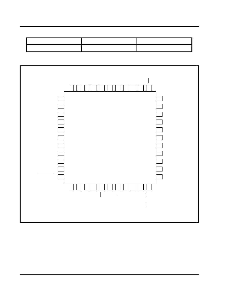
IGURE
2. P
IN
O
UT
OF
THE
XRT73LC00
IN
THE
44 P
IN
TQFP
LC V /(RCLK2)
44
43
42
41
40
39
38
37
36
35
34
12
13
14
15
16
17
18
19
20
21
22
23
24
33
32
31
30
29
28
27
26
25
X R T 7 3 L C 0 0
(T o p V ie w )
TxLEV
TAO S
T xA VD D
D M O
T xA G N D
R T IP
A G N D
R xAG N D
R R IN G
R xA V D D
R E G R E SE T/
R C LK2IN V
R
EQD
I
S
L
OST
HR
LLB
RL
B
ST
S1
/
D
S
3
E3
H
OST
/
H
W
SD
I
/
(
L
OSMU
T
E
N)
SD
O/
(
L
C
V
)
S
C
L
K
/
(
E
NDE
CD
I
S
)
CS
/
(
DR/
SR
)
R P O S
R N E G
R C LK1
R xD V D D
D V D D
R xD G N D
E XC LK
D G N D
R LO S
R LO L
MT
I
P
MR
I
N
G
T
x
AV
DD
TTI
P
TRI
NG
T
x
AGN
D
TNDA
TA
TPD
A
TA
TCL
K
TX
OFF
IC
T
11
10
1
2
3
4
5
6
7
8
9

·Á
·Á
·Á
·Á
XRT73LC00
E3/DS3/STS-1 LINE INTERFACE UNIT
PRELIMINARY
REV. P1.0.1
I
TABLE OF CONTENTS
GENERAL DESCRIPTION .................................................................................................. 1
FEATURES ................................................................................................................................................ 1
APPLICATIONS ......................................................................................................................................... 1
Figure 1. Block Diagram of the XRT73LC00 .................................................................................................... 1
ORDERING INFORMATION ............................................................................................... 2
Figure 2. Pin Out of the XRT73LC00 in the 44 Pin TQFP ................................................................................ 2
TABLE OF CONTENTS ......................................................................................................... I
PIN DESCRIPTION ............................................................................................................. 3
ELECTRICAL CHARACTERISTICS ................................................................................. 11
ABSOLUTE MAXIMUM RATINGS ................................................................................................... 11
DC E
LECTRICAL
C
HARACTERISTICS
............................................................................................................ 11
AC E
LECTRICAL
C
HARACTERISTICS
............................................................................................................ 12
Figure 3. Timing Diagram of the Transmit Terminal Input Interface ............................................................... 13
Figure 4. Timing Diagram of the Receive Terminal Output Interface ............................................................. 13
Figure 5. Transmit Pulse Amplitude Test Circuit for DS3, E3 and STS-1 Rates ............................................ 13
AC ELECTRICAL CHARACTERISTICS (CONT'D) L
INE
S
IDE
P
ARAMETERS
........................................... 16
Figure 6. ITU-T G.703 Transmit Output Pulse Template for E3 Applications ................................................. 17
Figure 7. Bellcore GR-499-CORE Transmit Output Pulse Template for DS3 Applications ............................ 17
Figure 8. Bellcore GR-253-CORE Transmit Output Pulse Template for SONET STS-1 Applications ........... 18
Figure 9. Microprocessor Serial Interface Data Structure .............................................................................. 18
AC ELECTRICAL CHARACTERISTICS (CONT.) ................................................................................... 19
Figure 10. Timing Diagram for the Microprocessor Serial Interface ............................................................... 19
SYSTEM DESCRIPTION ................................................................................................... 20
T
HE
T
RANSMIT
S
ECTION
............................................................................................................................ 20
T
HE
R
ECEIVE
S
ECTION
.............................................................................................................................. 20
T
HE
M
ICROPROCESSOR
S
ERIAL
I
NTERFACE
................................................................................................ 20
T
ABLE
1: R
OLE
OF
M
ICROPROCESSOR
S
ERIAL
I
NTERFACE
PINS
WHEN
THE
XRT73LC00
IS
OPERATING
IN
THE
H
ARD
-
WARE
M
ODE
...................................................................................................................................... 20
1.0 Selecting the Data Rate ............................................................................................. 21
T
ABLE
2: S
ELECTING
THE
D
ATA
R
ATE
FOR
THE
XRT73LC00
VIA
THE
E3
AND
STS-1/DS3
INPUT
PINS
(H
ARDWARE
M
ODE
) ............................................................................................................................................... 21
C
OMMAND
R
EGISTER
CR4 (A
DDRESS
= 0
X
04) ........................................................................................... 21
T
ABLE
3: S
ELECTING
THE
D
ATA
R
ATE
FOR
THE
XRT73LC00 V
IA
THE
STS-1/DS3
AND
THE
E3 B
IT
-
FIELDS
W
ITHIN
C
OMMAND
R
EGISTER
CR4 (HOST M
ODE
) .......................................................................................... 21
2.0 The Transmit Section ................................................................................................ 22
2.1 T
HE
T
RANSMIT
L
OGIC
B
LOCK
.............................................................................................................. 22
Figure 11. The Typical Interface for the Transmission of Data in a Dual-Rail Format From the Transmitting Ter-
minal Equipment to the Transmit Section of the XRT73LC00 ...................................................... 22
Figure 12. How the XRT73LC00 Samples the Data on the TPDATA and TNDATA Input Pins ..................... 22
2.1.1 Accepting Single-Rail Data from the Terminal Equipment ................................................. 23
C
OMMAND
R
EGISTER
CR1 (A
DDRESS
= 0
X
01) ........................................................................................... 23
Figure 13. The Behavior of the TPDATA and TCLK Input Signals While the Transmit Logic Block is Accepting
Single-Rail Data From the Terminal Equipment ........................................................................... 23
2.2 T
HE
T
RANSMIT
C
LOCK
D
UTY
C
YCLE
A
DJUST
C
IRCUITRY
...................................................................... 23
2.3 T
HE
HDB3/B3ZS E
NCODER
B
LOCK
.................................................................................................... 24
2.3.1 B3ZS Encoding ....................................................................................................................... 24
Figure 14. An Example of B3ZS Encoding ..................................................................................................... 24
2.3.2 HDB3 Encoding ...................................................................................................................... 24
Figure 15. An Example of HDB3 Encoding .................................................................................................... 24
2.3.3 Enabling/Disabling the HDB3/B3ZS Encoder ...................................................................... 25
2.4 T
HE
T
RANSMIT
P
ULSE
S
HAPER
C
IRCUITRY
........................................................................................... 25

XRT73LC00
E3/DS3/STS-1 LINE INTERFACE UNIT
·Á
·Á
·Á
·Á
REV. P1.0.1
PRELIMINARY
II
C
OMMAND
R
EGISTER
CR2 (A
DDRESS
= 0
X
02) ............................................................................................ 25
2.4.1 Enabling the Transmit Line Build-Out Circuit ...................................................................... 25
C
OMMAND
R
EGISTER
CR1 (A
DDRESS
= 0
X
01) ............................................................................................ 25
2.4.2 Disabling the Transmit Line Build-Out Circuit ..................................................................... 26
2.4.3 Design Guideline for Setting the Transmit Line Build-Out Circuit ..................................... 26
C
OMMAND
R
EGISTER
CR1 (A
DDRESS
= 0
X
01) ............................................................................................ 26
2.4.4 The Transmit Line Build-Out Circuit and E3 Applications .................................................. 26
2.5 I
NTERFACING
THE
T
RANSMIT
S
ECTION
OF
THE
XRT73LC00
TO
THE
L
INE
.............................................. 26
Figure 16. Recommended Schematic for Interfacing the Transmit Section of the XRT73LC00 to the Line ... 26
T
RANSFORMER
R
ECOMMENDATIONS
............................................................................................... 27
3.0 The Receive Section ................................................................................................. 28
3.1 I
NTERFACING
THE
R
ECEIVE
S
ECTION
OF
THE
XRT73LC00
TO
THE
L
INE
................................................ 28
Figure 17. Recommended Schematic for Interfacing the Receive Section of the XRT73LC00 to the Line (Trans-
former-Coupling) ........................................................................................................................... 28
Figure 18. Recommended Schematic for Interfacing the Receive Section of the XRT73LC00 to the Line (Capac-
itive-Coupling) ............................................................................................................................... 28
3.2 T
HE
R
ECEIVE
E
QUALIZER
B
LOCK
......................................................................................................... 28
3.2.1 Guidelines for Setting the Receive Equalizer ....................................................................... 29
Figure 19. The Typical Application for the System Installer ........................................................................... 30
3.3 P
EAK
D
ETECTOR
AND
S
LICER
............................................................................................................... 31
3.4 C
LOCK
R
ECOVERY
PLL ....................................................................................................................... 31
C
OMMAND
R
EGISTER
CR2 (A
DDRESS
= 0
X
02) ............................................................................................ 31
3.5 T
HE
HDB3/B3ZS D
ECODER
................................................................................................................ 31
3.5.1 B3ZS Decoding DS3/STS-1 Applications .............................................................................. 31
Figure 20. An Example of B3ZS Decoding ..................................................................................................... 32
3.5.2 HDB3 Decoding E3 Applications ........................................................................................... 32
Figure 21. An Example of HDB3 Decoding ..................................................................................................... 32
3.5.3 Enabling/Disabling the HDB3/B3ZS Decoder ....................................................................... 32
3.6 LOS D
ECLARATION
/C
LEARANCE
.......................................................................................................... 33
C
OMMAND
R
EGISTER
CR2 (A
DDRESS
= 0
X
02) ............................................................................................ 33
3.6.1 The LOS Declaration/Clearance Criteria for E3 Applications ............................................. 33
Figure 22. The Signal Levels that the XRT73LC00 Declares and Clears LOS (E3 Mode Only) ..................... 33
Figure 23. The Behavior of the LOS Output Indicator In Response to the Loss of Signal and the Restoration of
Signal ............................................................................................................................................ 34
3.6.2 The LOS Declaration/Clearance Criteria for DS3 and STS-1 Applications ........................ 34
T
ABLE
4: T
HE
ALOS (A
NALOG
LOS) D
ECLARE
AND
C
LEAR
T
HRESHOLDS
FOR
A
GIVEN
SETTING
OF
LOSTHR
AND
REQEN
FOR
DS3
AND
STS-1 A
PPLICATIONS
..................................................................................... 34
C
OMMAND
R
EGISTER
CR0 (A
DDRESS
= 0
X
00) ............................................................................................ 35
C
OMMAND
R
EGISTER
CR2 (A
DDRESS
= 0
X
02) ............................................................................................ 35
3.6.3 Muting the Recovered Data while the LOS is being Declared ............................................ 35
C
OMMAND
R
EGISTER
CR0 (A
DDRESS
= 0
X
00) ............................................................................................ 35
C
OMMAND
R
EGISTER
CR2 (A
DDRESS
= 0
X
02) ............................................................................................ 35
3.7 R
OUTING
THE
R
ECOVERED
T
IMING
AND
D
ATA
I
NFORMATION
TO
THE
R
ECEIVING
T
ERMINAL
E
QUIPMENT
.. 36
C
OMMAND
R
EGISTER
CR3 (A
DDRESS
= 0
X
03) ............................................................................................ 36
Figure 24. The Typical Interface for the Transmission of Data in a Dual-Rail Format From the Receive Section
of the XRT73LC00 to the Receiving Terminal Equipment ............................................................ 36
Figure 25. How the XRT73LC00 Outputs Data on the RPOS and RNEG Output Pins ................................. 37
Figure 26. The Behavior of the RPOS, RNEG and RCLK1 Signals When RCLK1 is Inverted ....................... 37
C
OMMAND
R
EGISTER
CR3 (A
DDRESS
= 0
X
03) ............................................................................................ 37
3.7.1 Routing Single-Rail Format data (Binary Data Stream) to the Receive Terminal Equipment
37
C
OMMAND
R
EGISTER
CR3 (A
DDRESS
= 0
X
03) ............................................................................................ 38
Figure 27. The Typical Interface for the Transmission of Data in a Single-Rail Format From the Receive Section
of the XRT73LC00 to the Receiving Terminal Equipment ............................................................ 38

·Á
·Á
·Á
·Á
XRT73LC00
E3/DS3/STS-1 LINE INTERFACE UNIT
PRELIMINARY
REV. P1.0.1
III
Figure 28. The Behavior of the RPOS and RCLK1 Output Signals While the XRT73LC00 is Transmitting Single-
Rail Data to the Receiving Terminal Equipment ........................................................................... 38
4.0 Diagnostic Features of the XRT73LC00 ................................................................... 38
4.1 T
HE
A
NALOG
L
OCAL
L
OOP
-B
ACK
M
ODE
.............................................................................................. 38
Figure 29. The Analog Local Loop-Back in the XRT73LC00 .......................................................................... 39
C
OMMAND
R
EGISTER
CR4 (A
DDRESS
= 0
X
04) ........................................................................................... 39
4.2 T
HE
D
IGITAL
L
OCAL
L
OOP
-B
ACK
M
ODE
............................................................................................... 39
Figure 30. The Digital Local Loop-Back path in the XRT73LC00 ................................................................... 40
C
OMMAND
R
EGISTER
CR4 (A
DDRESS
= 0
X
04) ........................................................................................... 40
4.3 T
HE
R
EMOTE
L
OOP
-B
ACK
M
ODE
......................................................................................................... 40
Figure 31. The Remote Loop-Back Path in the XRT73LC00 ......................................................................... 41
4.4 TXOFF F
EATURES
.............................................................................................................................. 41
C
OMMAND
R
EGISTER
CR4 (A
DDRESS
= 0
X
04) ........................................................................................... 41
4.5 T
HE
T
RANSMIT
D
RIVE
M
ONITOR
F
EATURES
.......................................................................................... 41
C
OMMAND
R
EGISTER
CR1 (A
DDRESS
= 0
X
01) ........................................................................................... 41
Figure 32. The XRT73LC00 Employing the Transmit Drive Monitor Features ............................................... 42
Figure 33. Two LIU's, Each Monitoring the Transmit Output Signal of the Other LIU IC .............................. 43
4.6 T
HE
TAOS (T
RANSMIT
A
LL
O
NE
S) F
EATURE
....................................................................................... 43
C
OMMAND
R
EGISTER
CR1 (A
DDRESS
= 0
X
01) ........................................................................................... 43
5.0 The Microprocessor Serial Interface ........................................................................ 44
5.1 D
ESCRIPTION
OF
THE
C
OMMAND
R
EGISTERS
........................................................................................ 44
T
ABLE
5: A
DDRESSES
AND
B
IT
F
ORMATS
OF
XRT73LC00 C
OMMAND
R
EGISTERS
.............................................. 44
D
ESCRIPTION
OF
B
IT
-F
IELDS
FOR
E
ACH
C
OMMAND
REGISTER
..................................................................... 44
5.1.1 Command Register - CR0 ...................................................................................................... 44
5.1.2 Command Register - CR1 ...................................................................................................... 45
5.1.3 Command Register - CR2 ...................................................................................................... 46
5.1.4 Command Register - CR3 ...................................................................................................... 46
5.1.5 Command Register - CR4 ...................................................................................................... 46
5.2 O
PERATING
THE
M
ICROPROCESSOR
S
ERIAL
I
NTERFACE
. ...................................................................... 47
T
ABLE
6: L
OOP
-B
ACK
M
ODES
........................................................................................................................... 47
Figure 34. Microprocessor Serial Interface Data Structure ............................................................................ 48
O
RDERING
I
NFORMATION
............................................................................................................................ 49
PACKAGE DIMENSIONS ................................................................................................. 49
R
EVISION
H
ISTORY
..................................................................................................................................... 50