 | ÐлекÑÑоннÑй компоненÑ: XRT75L06 | СкаÑаÑÑ:  PDF PDF  ZIP ZIP |
Untitled Document
Exar
Corporation 48720 Kato Road, Fremont CA, 94538
·
(510) 668-7000
·
FAX (510) 668-7017
·
www.exar.com
XRT75L06
SIX CHANNEL E3/DS3/STS-1 LINE INTERFACE UNIT WITH JITTER ATTENUATOR
OCTOBER 2003
REV. 1.0.2
GENERAL DESCRIPTION
The XRT75L06 is a six channel fully integrated Line
Interface Unit (LIU) for E3/DS3/STS-1 applications.
The LIU incorporates 6 independent Receivers,
Transmitters and Jitter Attenuators in a single 217
Lead BGA package.
Each channel of the XRT75L06 can be independently
configured to operate in E3 (34.368 MHz), DS3
(44.736 MHz) or STS-1 (51.84 MHz). Each
transmitter can be turned off and tri-stated for
redundancy support or for conserving power.
The XRT75L06's differential receiver provides high
noise interference margin and is able to receive data
over 1000 feet of cable or with up to 12 dB of cable
attenuation.
The XRT75L06 incorporates an advanced crystal-
less jitter attenuator per channel that can be selected
either in the transmit or receive path. The jitter
attenuator performance meets the ETSI TBR-24 and
Bellcore GR-499 specifications.
The XRT75L06 provides a Parallel Microprocessor
Interface for programming and control.
The XRT75L06 supports analog, remote and digital
loop-backs. The device also has a built-in Pseudo
Random Binary Sequence (PRBS) generator and
detector with the ability to insert and detect single bit
error for diagnostic purposes.
APPLICATIONS
·
E3/DS3 Access Equipment
·
DSLAMs
·
Digital Cross Connect Systems
·
CSU/DSU Equipment
·
Routers
·
Fiber Optic Terminals
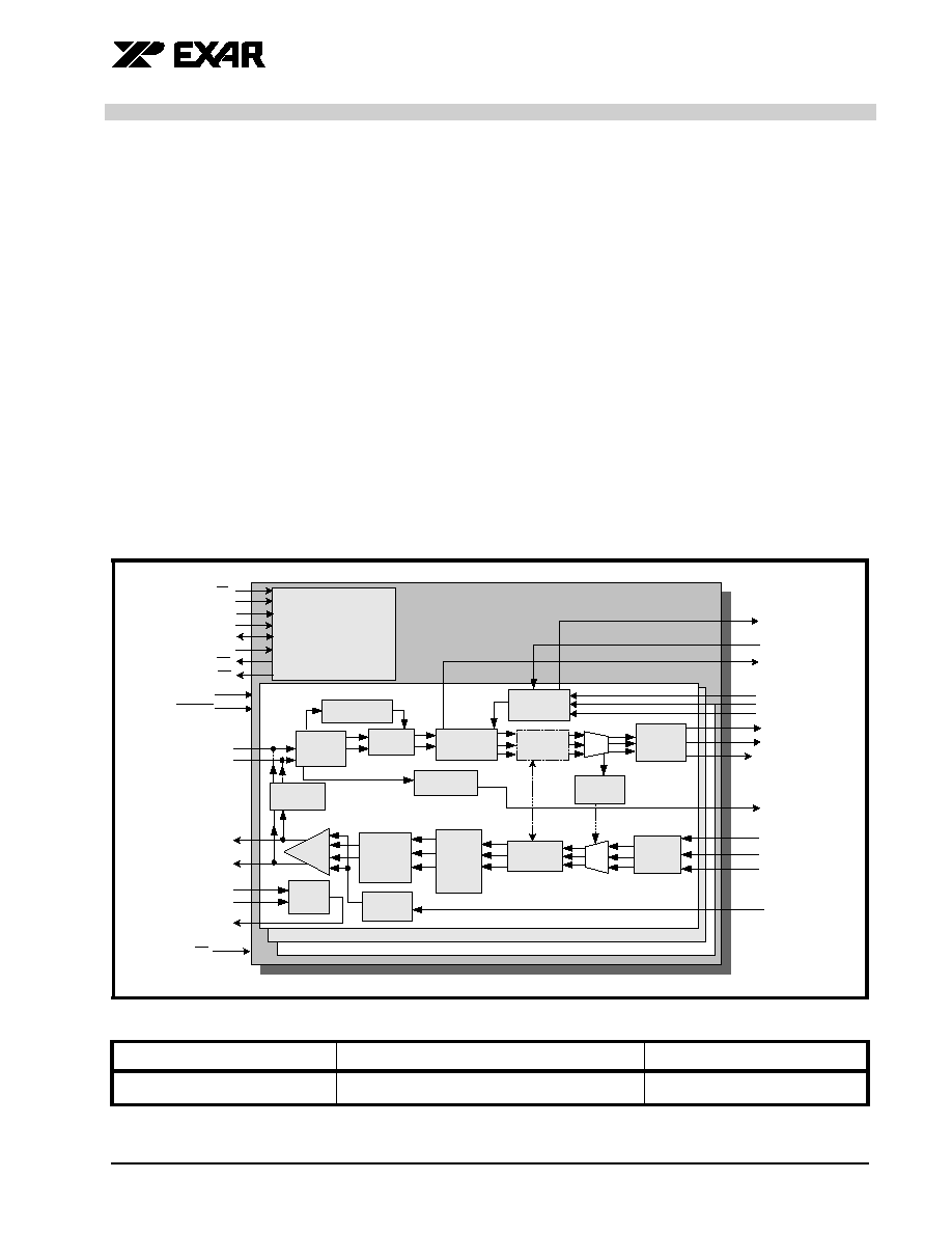
F
IGURE
1. B
LOCK
D
IAGRAM
OF
THE
XRT 75L06
ORDERING INFORMATION
P
ART
N
UMBER
P
ACKAGE
O
PERATING
T
EMPERATURE
R
ANGE
XRT75L06IB
217 Lead BGA
-40
°
C to +85
°
C
XRT75L06
XRT75L06
Channel 5
Channel 0
Channel n...
Device
Monitor
MTIP_n
MRing_n
DMO_n
Timing
Control
Tx
Pulse
Shaping
HDB3/
B3ZS
Encoder
Tx
Control
Jitter
Attenuator
MUX
Line
Driver
Remote
LoopBack
HDB3/
B3ZS
Decoder
MUX
AGC/
Equalizer
Peak Detector
LOS
Detector
Slicer
Jitter
Attenuator
µ
Processor Interface
Local
LoopBack
Clock & Data
Recovery
Clock
Synthesizer
RD
WR
Addr[7:0]
CS
INT
D[7:0]
TxON
TxClk_n
TxPOS_n
TxNEG_n
RxClk_n
RxPOS_n
RxNEG/LCV_n
RLOS_n
RLOL_n
RTIP_n
RRing_n
TTIP_n
TRing_n
CLKOUT_n
SFM_en
E3Clk
DS3Clk
STS-Clk/12M
ICT
Pmode
RDY
PCLK
RESET

XRT75L06
REV. 1.0.2
SIX CHANNEL E3/DS3/STS-1 LINE INTERFACE UNIT WITH JITTER ATTENUATOR
2
FEATURES
RECEIVER
·
On chip Clock and Data Recovery circuit for high
input jitter tolerance
·
Meets E3/DS3/STS-1 Jitter Tolerance Requirement
·
Detects and Clears LOS as per G.775
·
Receiver Monitor mode handles up to 20 dB flat
loss with 6 dB cable attenuation
·
On chip B3ZS/HDB3 encoder and decoder that can
be either enabled or disabled
·
On-chip clock synthesizer provides the appropriate
rate clock from a single 12.288 MHz Clock
·
Provides low jitter output clock
TRANSMITTER
·
Compliant with Bellcore GR-499, GR-253 and ANSI
T1.102 Specification for transmit pulse
·
Tri-state Transmit output capability for redundancy
applications
·
Each Transmitter can be turned on or off
JITTER ATTENUATOR
·
On chip advanced crystal-less Jitter Attenuator for
each channel
·
Jitter Attenuator can be selected in Receive,
Transmit path, or disabled
·
Meets ETSI TBR 24 Jitter Transfer Requirements
·
Compliant with jitter transfer template outlined in
ITU G.751, G.752, G.755 and GR-499-CORE,1995
standards
·
16 or 32 bits selectable FIFO size
CONTROL AND DIAGNOSTICS
·
Parallel Microprocessor Interface for control and
configuration
·
Supports optional internal Transmit driver
monitoring
·
Each channel supports Analog, Remote and Digital
Loop-backs
·
Single 3.3 V ± 5% power supply
·
5 V Tolerant digital inputs
·
Available in 217 pin BGA Package
·
- 40°C to 85°C Industrial Temperature Range
TRANSMIT INTERFACE CHARACTERISTICS
·
Accepts either Single-Rail or Dual-Rail data from
Terminal Equipment and generates a bipolar signal
to the line
·
Integrated Pulse Shaping Circuit
·
Built-in B3ZS/HDB3 Encoder (which can be
disabled)
·
Accepts Transmit Clock with duty cycle of 30%-
70%
·
Generates pulses that comply with the ITU-T G.703
pulse template for E3 applications
·
Generates pulses that comply with the DSX-3 pulse
template, as specified in Bellcore GR-499
-CORE
and ANSI T1.102_1993
·
Generates pulses that comply with the STSX-1
pulse template, as specified in Bellcore GR-253-
CORE
·
Transmitter can be turned off in order to support
redundancy designs
RECEIVE INTERFACE CHARACTERISTICS
·
Integrated Adaptive Receive Equalization (optional)
for optimal Clock and Data Recovery
·
Declares and Clears the LOS defect per ITU-T
G.775 requirements for E3 and DS3 applications
·
Meets Jitter Tolerance Requirements, as specified
in ITU-T G.823_1993 for E3 Applications
·
Meets Jitter Tolerance Requirements, as specified
in Bellcore GR-499-CORE for DS3 Applications
·
Declares Loss of Lock (LOL) Alarm
·
Built-in B3ZS/HDB3 Decoder (which can be
disabled)
·
Recovered Data can be muted while the LOS
Condition is declared
·
Outputs either Single-Rail or Dual-Rail data to the
Terminal Equipment
XRT75L06
SIX CHANNEL E3/DS3/STS-1 LINE INTERFACE UNIT WITH JITTER ATTENUATOR
REV. 1.0.2
3
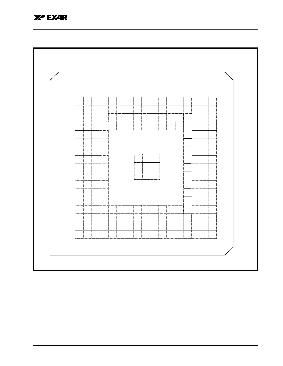
F
IGURE
2. XRT75L06
IN
BGA
PACKAGE
(B
OTTOM
V
IEW
)
1
17
16
15
14
12
12
3
2
7
6
5
4
11
10
9
8
U
T
R
P
N
M
L
K
J
H
G
F
E
D
C
B
A
(See pin list for pin names and function)
XRT75L06

XRT75L06
SIX CHANNEL E3/DS3/STS-1 LINE INTERFACE UNIT WITH JITTER ATTENUATOR
REV. 1.0.2
I
TABLE OF CONTENTS
GENERAL DESCRIPTION ................................................................................................. 1
A
PPLICATIONS
.............................................................................................................................................. 1
Figure 1. Block Diagram of the XRT 75L06 ...................................................................................................... 1
ORDERING INFORMATION ................................................................................................................... 1
F
EATURES
.................................................................................................................................................... 2
T
RANSMIT
I
NTERFACE
C
HARACTERISTICS
...................................................................................................... 2
R
ECEIVE
I
NTERFACE
C
HARACTERISTICS
........................................................................................................ 2
Figure 2. XRT75L06 in BGA package (Bottom View) ....................................................................................... 3
PIN DESCRIPTIONS (BY FUNCTION) .............................................................................. 4
T
RANSMIT
I
NTERFACE
................................................................................................................................... 4
R
ECEIVE
I
NTERFACE
..................................................................................................................................... 6
C
LOCK
I
NTERFACE
........................................................................................................................................ 8
CONTROL AND ALARM INTERFACE ....................................................................................................... 9
A
NALOG
P
OWER
AND
G
ROUND
................................................................................................................... 12
DIGITAL
P
OWER
AND
G
ROUND
..................................................................................................................... 14
1.0 clock Synthesizer ............................................................................................................................. 16
1.1 C
LOCK
D
ISTRIBUTION
....................................................................................................................................... 16
Figure 4. Clock Distribution Congifured in E3 Mode Without Using SFM ....................................................... 16
Figure 3. Simplified Block Diagram of the Input Clock Circuitry Driving the Microprocessor .......................... 16
2.0 The Receiver Section ....................................................................................................................... 17
Figure 5. Receive Path Block Diagram ........................................................................................................... 17
2.1 R
ECEIVE
L
INE
I
NTERFACE
................................................................................................................................. 17
Figure 6. Receive Line InterfaceConnection ................................................................................................... 17
2.2 A
DAPTIVE
G
AIN
C
ONTROL
(AGC) ..................................................................................................................... 18
2.3 R
ECEIVE
E
QUALIZER
........................................................................................................................................ 18
Figure 7. ACG/Equalizer Blcok Diagram ......................................................................................................... 18
2.3.1 Recommendations for Equalizer Settings ....................................................................................... 18
2.4 C
LOCK
AND
D
ATA
R
ECOVERY
.......................................................................................................................... 18
2.4.1 Data/Clock Recovery Mode ............................................................................................................... 18
2.4.2 Training Mode ..................................................................................................................................... 18
2.5 LOS (L
OSS
OF
S
IGNAL
) D
ETECTOR
.................................................................................................................. 19
2.5.1 DS3/STS-1 LOS Condition ................................................................................................................. 19
2.5.2 Disabling ALOS/DLOS Detection ...................................................................................................... 19
T
ABLE
1: T
HE
ALOS (A
NALOG
LOS) D
ECLARATION
AND
C
LEARANCE
T
HRESHOLDS
FOR
A
GIVEN
SETTING
OF
LOSTHR
AND
REQEN (DS3
AND
STS-1 A
PPLICATIONS
) ................................................................... 19
2.5.3 E3 LOS Condition: ............................................................................................................................. 20
Figure 8. Loss Of Signal Definition for E3 as per ITU-T G.775 ....................................................................... 20
Figure 9. Loss of Signal Definition for E3 as per ITU-T G.775. ....................................................................... 20
2.5.4 Interference Tolerance ....................................................................................................................... 21
Figure 10. Interference Margin Test Set up for DS3/STS-1 ............................................................................ 21
Figure 11. Interference Margin Test Set up for E3. ......................................................................................... 21
T
ABLE
2: I
NTERFERENCE
M
ARGIN
T
EST
R
ESULTS
.............................................................................................. 22
2.5.5 Muting the Recovered Data with LOS condition: ............................................................................ 23
2.6 B3ZS/HDB3 D
ECODER
.................................................................................................................................... 23
Figure 12. Receiver Data output and code violation timing ............................................................................ 23
3.0 The Transmitter Section .................................................................................................................. 24
Figure 13. Transmit Path Block Diagram ........................................................................................................ 24
3.1 T
RANSMIT
D
IGITAL
I
NPUT
I
NTERFACE
................................................................................................................ 24
Figure 14. Typical interface between terminal equipment and the XRT75L06 (dual-rail data) ....................... 24
Figure 15. Transmitter Terminal Input Timing ................................................................................................. 25
Figure 16. Single-Rail or NRZ Data Format (Encoder and Decoder are Enabled) ......................................... 25
3.2 T
RANSMIT
C
LOCK
............................................................................................................................................ 26
3.3 B3ZS/HDB3 E
NCODER
.................................................................................................................................... 26

XRT75L06
SIX CHANNEL E3/DS3/STS-1 LINE INTERFACE UNIT WITH JITTER ATTENUATOR
REV. 1.0.2
II
3.3.1 B3ZS Encoding .................................................................................................................................. 26
3.3.2 HDB3 Encoding .................................................................................................................................. 26
Figure 17. Dual-Rail Data Format (encoder and decoder are disabled) ......................................................... 26
Figure 18. B3ZS Encoding Format ................................................................................................................. 26
3.4 T
RANSMIT
P
ULSE
S
HAPER
............................................................................................................................... 27
Figure 20. Transmit Pulse Shape Test Circuit ................................................................................................ 27
3.4.1 Guidelines for using Transmit Build Out Circuit ............................................................................. 27
Figure 19. HDB3 Encoding Format ................................................................................................................ 27
3.5 E3
LINE
SIDE
PARAMETERS
.............................................................................................................................. 28
Figure 21. Pulse Mask for E3 (34.368 mbits/s) interface as per itu-t G.703 ................................................... 28
T
ABLE
3: E3 T
RANSMITTER
LINE
SIDE
OUTPUT
AND
RECEIVER
LINE
SIDE
INPUT
SPECIFICATIONS
.......................... 29
Figure 22. Bellcore GR-253 CORE Transmit Output Pulse Template for SONET STS-1 Applications ......... 30
T
ABLE
4: STS-1 P
ULSE
M
ASK
E
QUATIONS
........................................................................................................ 30
T
ABLE
5: STS-1 T
RANSMITTER
L
INE
S
IDE
O
UTPUT
AND
R
ECEIVER
L
INE
S
IDE
I
NPUT
S
PECIFICATIONS
(GR-253) . 31
Figure 23. Transmit Ouput Pulse Template for DS3 as per Bellcore GR-499 ................................................ 31
T
ABLE
7: DS3 T
RANSMITTER
L
INE
S
IDE
O
UTPUT
AND
R
ECEIVER
L
INE
S
IDE
I
NPUT
S
PECIFICATIONS
(GR-499) .... 32
T
ABLE
6: DS3 P
ULSE
M
ASK
E
QUATIONS
........................................................................................................... 32
3.6 T
RANSMIT
D
RIVE
M
ONITOR
.............................................................................................................................. 33
3.7 T
RANSMITTER
S
ECTION
O
N
/O
FF
....................................................................................................................... 33
Figure 24. Transmit Driver Monitor set-up. ..................................................................................................... 33
4.0 Jitter .................................................................................................................................................. 34
4.1 J
ITTER
T
OLERANCE
.......................................................................................................................................... 34
4.1.1 DS3/STS-1 Jitter Tolerance Requirements ...................................................................................... 34
Figure 25. Jitter Tolerance Measurements ..................................................................................................... 34
4.1.2 E3 Jitter Tolerance Requirements .................................................................................................... 35
Figure 26. Input Jitter Tolerance For DS3/STS-1 .......................................................................................... 35
Figure 27. Input Jitter Tolerance for E3 ......................................................................................................... 35
4.2 J
ITTER
T
RANSFER
............................................................................................................................................ 36
4.3 J
ITTER
A
TTENUATOR
........................................................................................................................................ 36
T
ABLE
8: J
ITTER
A
MPLITUDE
VERSUS
M
ODULATION
F
REQUENCY
(J
ITTER
T
OLERANCE
) ....................................... 36
T
ABLE
9: J
ITTER
T
RANSFER
S
PECIFICATION
/R
EFERENCES
................................................................................. 36
4.3.1 Jitter Generation ................................................................................................................................ 37
T
ABLE
10: J
ITTER
T
RANSFER
P
ASS
M
ASKS
....................................................................................................... 37
Figure 28. Jitter Transfer Requirements and Jitter Attenuator Performance .................................................. 37
5.0 Diagnostic Features ......................................................................................................................... 38
5.1 PRBS G
ENERATOR
AND
D
ETECTOR
................................................................................................................. 38
Figure 29. PRBS MODE ................................................................................................................................. 38
5.2 LOOPBACKS ................................................................................................................................................ 39
5.2.1 ANALOG LOOPBACK ........................................................................................................................ 39
Figure 30. Analog Loopback ........................................................................................................................... 39
5.2.2 DIGITAL LOOPBACK ......................................................................................................................... 40
5.2.3 REMOTE LOOPBACK ........................................................................................................................ 40
Figure 31. Digital Loopback ............................................................................................................................ 40
Figure 32. Remote Loopback ......................................................................................................................... 40
5.3 TRANSMIT ALL ONES (TAOS) .................................................................................................................... 41
Figure 33. Transmit All Ones (TAOS) ............................................................................................................. 41
6.0 Microprocessor interface Block ..................................................................................................... 42
T
ABLE
11: S
ELECTING
THE
M
ICROPROCESSOR
I
NTERFACE
M
ODE
...................................................................... 42
Figure 34. Simplified Block Diagram of the Microprocessor Interface Block .................................................. 42
6.1 T
HE
M
ICROPROCESSOR
I
NTERFACE
B
LOCK
S
IGNALS
........................................................................................ 43
T
ABLE
12: XRT75L06 M
ICROPROCESSOR
I
NTERFACE
S
IGNALS
......................................................................... 43
6.2 A
SYNCHRONOUS
AND
S
YNCHRONOUS
D
ESCRIPTION
......................................................................................... 44
T
ABLE
13: A
SYNCHRONOUS
T
IMING
S
PECIFICATIONS
......................................................................................... 45
Figure 35. Asynchronous µP Interface Signals During Programmed I/O Read and Write Operations ........... 45
Figure 36. Synchronous µP Interface Signals During Programmed I/O Read and Write Operations ............ 46
T
ABLE
14: S
YNCHRONOUS
T
IMING
S
PECIFICATIONS
........................................................................................... 46
Document Outline