
Exar
Corporation 48720 Kato Road, Fremont CA, 94538
∑
(510) 668-7000
∑
FAX (510) 668-7017
∑
www.exar.com
·Á
·Á
·Á
·Á
PRELIMINARY
XRT79L71
1 - CHANNEL DS3/E3 ATM UNI/PPP COMBO IC
JUNE 2003
REV. P1.0.3
GENERAL DESCRIPTION
The XRT79L71 is a single channel, ATM UNI/PPP
Physical Layer Processor with integrated DS3/E3
framing controller and Line Interface Unit with Jitter
Attenuator that is designed to support ATM direct
mapping and cell delineation as well as PPP mapping
and Frame processing. For ATM UNI applications,
this device provides the ATM Physical Layer (Physical
Medium Dependent and Transmission Convergence
sub-layers) interface for the public and private net-
works at DS3/E3 rates. For Clear-Channel Framer
applications, this device supports the transmission
and reception of "user data" via the DS3/E3 payload.
The XRT79L71 includes DS3/E3 Framing, Line
Interface Unit with Jitter Attenuator that supports
mapping of ATM or HDLC framed data. A flexible
parallel microprocessor interface is provided for
configuration and control. Industry standard UTOPIA II
and POS-PHY interface are also provided.
GENERAL FEATURES:
∑
Integrated T3/E3 Line Interface Unit
∑
Integrated Jitter Attenuator that can be selected
either in Receive or Transmit path
∑
Flexible integrated Clock Multiplier that takes single
frequency clock and generates either DS3 or E3
frequency.
∑
8/16 bit UTOPIA Level I and II and PPP Multi-PHY
Interface operating at 25, 33 or 50 MHz.
∑
HDLC Controller that provides the mapping/
extraction of either bit or byte mapped
encapsulated packet from DS3/E3 Frame.
∑
Contains on-chip 16 cell FIFO (configurable in
depths of 4, 8, 12 or 16 cells), in both the Transmit
(TxFIFO) and Receive Directions (RxFIFO)
∑
Contains on-chip 54 byte Transmit and Receive
OAM Cell Buffer for transmission, reception and
processing of OAM Cells
∑
Supports ATM cell or PPP Packet Mapping
∑
Supports M13 and C-Bit Parity Framing Formats
∑
Supports DS3/E3 Clear-Channel Framing.
∑
Includes PRBS Generator and Receiver
∑
Supports Line, Cell, and PLCP Loop-backs
∑
Interfaces to 8 Bit wide Intel, Motorola, PowerPC,
and Mips µPs
∑
Low power 3.3V, 5V Input Tolerant, CMOS
∑
Available in 208 STBl PBGA Package
∑
JTAG Interface
L
INE
I
NTERFACE
U
NIT
∑
On chip Clock and Data Recovery circuit for high
input jitter tolerance
∑
Meets E3/DS3 Jitter Tolerance Requirements
∑
Detects and Clears LOS as per G.775.
∑
Receiver Monitor mode handles up to 20 dB flat
loss with 6 dB cable attenuation
∑
Compliant with jitter transfer template outlined in
ITU G.751, G.752, G.755 and GR-499-CORE,1995
standards
∑
Meets ETSI TBR 24 and GR-499 Jitter Transfer
Requirements
∑
On chip B3ZS/HDB3 encoder and decoder that can
be either enabled or disabled
∑
On-chip clock synthesizer provides the appropriate
rate clock from a single 12.288 MHz Clock
∑
On chip advanced crystal-less Jitter Attenuator
∑
Jitter Attenuator can be selected in Receive or
Transmit paths
∑
16 or 32 bits selectable FIFO size
∑
Meets the Jitter and Wander specifications
described in T1.105.03b,ETSI TBR-24, Bellcore
GR-253 and GR-499 standards
∑
Jitter Attenuator can be disabled
∑
Typical power consumption 1.3W
DS3/E3 F
RAMER
∑
DS3 framer supports both M13 and C-bit parity.
∑
DS3 framer meets ANSI T1.107 and T1.404
standards.
∑
Detects OOF,LOF,AIS,RDI/FERF alarms.
∑
Generation and Insertion of FEBE on received
parity errors supported.
∑
Automatic insertion of RDI/FERF on alarm status.
∑
E3 framer meets G.832,G.751 standards.
∑
Framers can be bypassed.
ATM/PPP PROTOCOL PROCESSOR
T
RANSMIT
C
ELL
P
ROCESSING
∑
Extracts ATM cells
∑
Supports ATM cell payload scrambling
∑
Maps ATM cells into E3 or DS3 frame
∑
PLCP frame and mapping of ATM cell streams

XRT79L71
PRELIMINARY
·Á
·Á
·Á
·Á
REV. P1.0.3
1 - CHANNEL DS3/E3 ATM UNI/PPP COMBO IC
2
R
ECEIVE
C
ELL
P
ROCESSING
∑
Extraction of ATM cells from PLCP frame or directly
from E3 or DS3 frame
∑
Termination of PLCP frame
∑
Supports payload cell de-scrambling
T
RANSMIT
P
ACKET
P
ROCESSING
∑
Inserts PPP packets into data stream
∑
Maps HDLC data stream directly into DS3 or E3
frame
∑
Extracts in-band messaging packets
∑
Supports CRC-16/32, HDLC flag and Idle
sequence generation
R
ECEIVE
P
ACKET
P
ROCESSING
∑
Extracts HDLC data stream from DS3 or E3 frame
∑
Inserts in-band messaging packets
∑
Detects and removes HDLC flags
U
TOPIA
/ S
YSTEM
I
NTERFACE
∑
8/16 bit UTOPIA Level I and II and PPP Multi-PHY
Interface operating at 25, 33 or 50 MHz.
∑
Compliant with ATM Forum UTOPIA II interface
∑
Programmable FIFO size for both Transmit and
Receive direction
∑
Compliant to POS-PHY Level 2 interface
S
ERIAL
I
NTERFACE
∑
Serial clock and data interface for accessing DS3/
E3 framer
∑
Serial clock and data interface for accessing cell/
packet processor
APPLICATIONS
∑
Digital Access and Cross Connect Systems
∑
3G Base Stations
∑
DSLAMs
∑
Digital, ATM, WAN and LAN Switches
PRODUCT ORDERING INFORMATION
F
IGURE
1. B
LOCK
D
IAGRAM
OF
THE
XRT79L71
TU -3
P O H
P roces sor
Jitter
A tte nuator
R x D S 3/
E 3
F ram er
P LC P &
O verh ead
U T O P IA /
P O S -P H Y
Inte rface
H D LC
C ontroller
2
R e c e iv e r B lo c k
TC
K
TM
S
TD
I
TD
O
TR
S
T
JT A G T est P ort
C lock &
D ata
R ec ov ery
A G C /
E qu alize r
R TIP
R R IN G
T ra n s m itte r B lo c k
A T M C ell
P roces sor
or P P P
P roces sor
U T O P IA /
P O S -P H Y
Inte rface
A T M C ell
P roces sor
or P P P
P roces sor
H D LC
C ontroller
P LC P &
O verh ead
Tx D S 3/
E 3
F ram er
Jitter
A tte nuator
Tim in g
C ontrol
P ulse
S ha per
T TIP
T R IN G
M icroproces sor Inte rface
PC
L
K
IN
T
BL
AS
T
A
DDR[
1
4
:
0
]
AL
E_
AS
CS
WR
RD
D
BEN
T
YPE[
2
:
0
]
D
A
T
A
[7
:0
]
RDY
_
D
T
A
C
K
12.288
M H z
C lk IN
C lock
S ynth esizer
E 3 C L K
D S 3 C L K
R ec eive
U topia
P O S -P H Y
Inte rface
Trans m it
U topia
P O S -P H Y
Inte rface
P
RODUCT
N
UMBER
P
ACKAGE
T
YPE
O
PERATING
T
EMPERATURE
R
ANGE
XRT79L71IB
17X17 mm 208 Ball Shrink Thin Ball Grid Array
-40∞C to +85∞C
·Á
·Á
·Á
·Á
PRELIMINARY
XRT79L71
1 - CHANNEL DS3/E3 ATM UNI/PPP COMBO IC
REV. P1.0.3
3
T
ABLE
1: P
IN
O
UT
OF
THE
XRT79L71 (TOP VIEW)
A
RX
G
F
CCLK
R
XPL
O
F
T
X
P
O
HF
RA
M
E
RX
NIB
_
2
R
X
SER
RX
CLK
RX
O
HCLK
RX
O
H
F
R
A
M
E
TX
N
I
B
_
0
T
X
NIB
F
RA
M
E
T
X
F
R
AM
ER
EF
TX
O
H
E
N
A
B
L
E
TX
A
I
S
E
N
PD
A
T
A
_
3
PD
A
T
A
_
7
P
AS_
L
B
RX
G
F
CM
S
B
R
X
PR
ED
T
X
P
O
HCL
K
RX
NIB
_
3
RX
O
U
T
C
LK
RX
F
R
A
M
E
R
X
O
H
EN
ABL
E
TX
N
O
B
_
3
TX
OH
I
N
D
TX
FR
A
M
E
TX
OH
F
R
A
M
E
T
X
O
HCLK
PD
A
T
A
_
2
PD
A
T
A
_
6
PBL
AS
T
_
L
PW
R
_
L
C
RX
UD
A
T
A
_13
T
X
G
F
CCLK
RX
G
F
C
RX
P
O
HF
RA
M
E
RX
NIB
_
0
RX
O
H
IND
RX
O
H
TX
N
O
B
_
2
T
XSE
R
T
X
INCLK
TX
OH
PD
A
T
A_
1
PD
A
T
A_
5
PR
D
Y
_
L
P
RD_L
P
A
DDR_0
D
RX
UD
A
T
A
_
9
RX
UD
A
T
A
_
12
RX
UD
A
T
A
_
15
RX
CP
RX
P
O
O
F
RX
NI
B
_
1
RX
LO
S
TX
N
I
B
_
1
TX
N
I
B
C
L
K
TX
OH
I
N
S
PD
A
T
A
PD
A
T
A_
4
PI
N
T
_
L
PC
S
_
L
P
A
DDR_1
P
A
DDR_2
E
RX
UD
A
T
A
_
5
RX
UD
A
T
A
_
8
RX
UD
A
T
A
_11
RX
UD
A
T
A
_14
P
A
DDR_6
P
A
DDR_5
P
A
DDR_4
P
A
DDR_3
F
RX
U
D
A
T
A
_
2
RX
U
D
A
T
A
_
4
RX
U
D
A
T
A
_
7
RX
UD
A
T
A
_10
DP
A
DDR_3
DP
A
DDR_2
DP
A
DDR_1
DP
A
DDR_0
G
RX
UD
A
T
A
_
1
RX
UD
A
T
A
_
0
RX
UD
A
T
A
_
3
RX
UD
A
T
A
_
6
VD
D
VD
D
VD
D
VD
D
DP
A
DDR_7
DP
A
DDR_6
DP
A
DDR_5
DP
A
DDR_4
H
RX
UCLA
V
RX
US
O
C
RX
UP
R
T
Y
RX
UE
N_L
GN
D
GN
D
GN
D
GN
D
D
A
_
SEL
VD
D
GN
D
PC
L
K
J
RX
U
A
DDR_
0
RX
U
A
DDR_
1
RX
U
A
DDR_
2
RX
U
A
DDR_
3
GN
D
GN
D
GN
D
GN
D
PD
B
E
N
_
L
PT
Y
PE_
2
PT
Y
PE_
1
PT
Y
PE_
0
K
RX
U
A
DDR_4
RX
UCLK
O
R
X
PEO
P
R
SX_
R
S
O
F
VD
D
VD
D
VD
D
VD
D
GP
O_
2
GP
O_
1
GP
O_
0
CLK
O
UT
L
RX
M
O
D
R
X
PER
R
RX
UCLK
T
SX_
T
S
O
F
GP
I
_
2
GP
I
_
1
GP
I
_
0
NIB
B
LE
I
N
T
F
M
T
X
UCL
K
T
XPER
TX
MO
D
T
X
UE
N_L
OG
N
D
RE
S
E
T
_
L
T
EST
MO
D
E
E3
C
L
K
N
T
XPEO
P
RX
P
D
V
A
L
T
X
UCLA
V
T
X
UD
A
T
A
_10
TX
U
D
A
T
A
_
4
TX
U
D
A
T
A
_
8
T
X
UD
A
T
A
_13
GP
I
O
_
1
TD
O
T
X
DG
ND
TX
D
V
D
D
TX
A
G
N
D
OV
D
D
VD
D
GN
D
CLK
G
ND
P
T
X
UCLK
O
T
X
U
A
DDR_4
TX
U
S
OC
TX
U
D
A
T
A
_
1
TX
U
D
A
T
A
_
5
TX
U
D
A
T
A
_
9
T
X
UD
A
T
A
_14
GP
I
O
_2
TD
I
MT
I
P
MR
I
N
G
RE
F
A
G
N
D
AN
A
I
O
1
AN
A
I
O
2
IC
T
B
DS
3CLK
R
T
X
U
A
DDR_3
T
X
U
A
DDR_2
TX
U
P
R
T
Y
TX
U
D
A
T
A
_
2
TX
U
D
A
T
A
_
6
T
X
UD
A
T
A
_11
T
X
UD
A
T
A
_15
GP
I
O
_3
TM
S
TR
S
T
NC
RE
F
A
V
D
D
RRI
NG
RT
I
P
TX
ON
C
L
KVD
D
T
T
X
U
A
DDR_1
T
X
U
A
DDR_0
TX
U
D
A
T
A
_
0
TX
U
D
A
T
_
3
TX
U
D
A
T
A
_
7
T
X
UD
A
T
A
_12
GP
I
O
_0
DM
O
_
0
TC
K
TR
I
N
G
TT
I
P
TX
A
V
D
D
RX
A
V
DD
RX
A
G
ND
JA
G
N
D
JA
A
V
D
D
1
2
3
4
5
6
7
8
9
10
11
12
13
14
15
16

XRT79L71
PRELIMINARY
·Á
·Á
·Á
·Á
REV. P1.0.3
1 - CHANNEL DS3/E3 ATM UNI/PPP COMBO IC
1
TABLE OF CONTENTS
GENERAL DESCRIPTION .................................................................................................1
GENERAL
F
EATURES
:......................................................................................................................................1
Line Interface Unit ....................................................................................................................................................... 1
DS3/E3 Framer............................................................................................................................................................ 1
ATM/PPP PROTOCOL PROCESSOR........................................................................................................................ 1
Transmit Cell Processing............................................................................................................................................. 1
Receive Cell Processing.............................................................................................................................................. 2
Transmit Packet Processing ........................................................................................................................................ 2
Receive Packet Processing ......................................................................................................................................... 2
Utopia/ System Interface ............................................................................................................................................. 2
Serial Interface ............................................................................................................................................................ 2
APPLICATIONS ...........................................................................................................................................2
F
IGURE
1. B
LOCK
D
IAGRAM
OF
THE
XRT79L71 ............................................................................................................................... 2
P
RODUCT
O
RDERING
I
NFORMATION
................................................................................................................2
T
ABLE
1: P
IN
O
UT
OF
THE
XRT79L71 (TOP VIEW) ........................................................................................................................ 3
T
ABLE
OF
C
ONTENTS
...........................................................................................................1
P
IN
D
ESCRIPTIONS
.........................................................................................................................................4
M
ICROPROCESSOR
I
NTERFACE
.......................................................................................................................4
T
EST
AND
D
IAGNOSTIC
...................................................................................................................................7
G
ENERAL
P
URPOSE
I
NPUT
AND
O
UTPUT
P
INS
.................................................................................................8
T
RANSMIT
S
YSTEM
S
IDE
I
NTERFACE
P
INS
.......................................................................................................8
R
ECEIVE
S
YSTEM
S
IDE
I
NTERFACE
P
INS
.......................................................................................................23
T
RANSMIT
L
INE
S
IDE
S
IGNALS
......................................................................................................................35
R
ECEIVE
L
INE
S
IDE
S
IGNALS
........................................................................................................................36
VDD P
INS
...................................................................................................................................................37
GND P
INS
...................................................................................................................................................38
N
OT
C
ONNECTED
P
INS
.................................................................................................................................38
ELECTRICAL CHARACTERISTICS ................................................................................39
AC ELECTRICAL CHARACTERISTIC INFORMATION ..................................................39
MICROPROCESSOR INTERFACE TIMING
FOR
R
EVISION
A S
ILICON
......................................................39
MICROPROCESSOR INTERFACE TIMING - ASYNCHRONOUS INTEL MODE.................................................... 39
T
ABLE
2: DC ELECTRICAL CHARACTERISTICSS..................................................................................................................... 39
Applies to all TTL-Level Input and CMOS Level Output pins - Ambient Temperature = 25∞C .................................. 39
F
IGURE
2. A
SYNCHRONUS
M
ODE
1 - I
NTEL
TYPE
P
ROGRAMMED
I/O T
IMING
(W
RITE
C
YCLE
) ............................................................ 39
F
IGURE
3. A
SYNCHRONUS
M
ODE
1 - I
NTEL
TYPE
P
ROGRAMMED
I/O T
IMING
(R
EAD
C
YCLE
) ............................................................. 40
T
ABLE
3: T
IMING
I
NFORMATION
FOR
THE
M
ICROPROCESSOR
I
NTERFACE
,
WHEN
CONFIGURED
TO
OPERATE
IN
THE
I
NTEL
A
SYNCHRONOUS
M
ODE
............................................................................................................................................................................ 40
MICROPROCESSOR INTERFACE TIMING - ASYNCHRONOUS MOTOROLA (68K)
MODE................................................................................................................................41
F
IGURE
4. A
SYNCHRONUS
M
ODE
2 - M
OTOROLA
68K P
ROGRAMMED
I/O T
IMING
(W
RITE
C
YCLE
) .................................................... 41
F
IGURE
5. A
SYNCHRONUS
M
ODE
2 - M
OTOROLA
68 P
ROGRAMMED
I/O T
IMING
(R
EAD
C
YCLE
) ........................................................ 41
MICROPROCESSOR INTERFACE TIMING - POWER PC 403 SYNCHRONOUS MODE42
T
ABLE
4: T
IMING
I
NFORMATION
FOR
THE
M
ICROPROCESSOR
I
NTERFACE
WHEN
CONFIGURED
TO
OPERATE
IN
THE
M
OTOROLA
(68K) A
SYN
-
CHRONOUS
M
ODE
........................................................................................................................................................... 42
F
IGURE
6. S
YNCHRONOUS
M
ODE
3 - IBM P
OWER
PC 403 I
NTERFACE
TIMING
(W
RITE
C
YCLE
) ......................................................... 42
F
IGURE
7. S
YNCHRONOUS
M
ODE
3 - IBM P
OWER
PC 403 I
NTERFACE
TIMING
(R
EAD
C
YCLE
)........................................................... 43
T
ABLE
5: T
IMING
I
NFORMATION
FOR
THE
M
ICROPROCESSOR
I
NTERFACE
,
WHEN
CONFIGURED
TO
OPERATE
IN
THE
IBM P
OWER
PC403
M
ODE
............................................................................................................................................................................ 43
MICROPROCESSOR INTERFACE TIMING - IDT3051/52 MODE ..................................44
F
IGURE
8. S
YNCHRONOUS
M
ODE
4 - IDT 3051/52 I
NTERFACE
TIMING
(W
RITE
C
YCLE
) .................................................................... 44
F
IGURE
9. S
YNCHRONOUS
M
ODE
4 - IDT 3051/52 I
NTERFACE
TIMING
(R
EAD
C
YCLE
)...................................................................... 45
T
ABLE
6: T
IMING
I
NFORMATION
FOR
THE
M
ICROPROCESSOR
I
NTERFACE
,
WHEN
CONFIGURED
TO
OPERATE
IN
THE
IBM P
OWER
PC403
M
ODE
............................................................................................................................................................................ 45
DS3/E3 LIU INTERFACE - LINE SIDE ELECTRICAL CHARACTERISTIC INFORMATION
46

·Á
·Á
·Á
·Á
PRELIMINARY
XRT79L71
1 - CHANNEL DS3/E3 ATM UNI/PPP COMBO IC
REV. P1.0.3
2
E3 L
INE
S
IDE
P
ARAMETERS
......................................................................................................................... 46
F
IGURE
10. P
ULSE
M
ASK
FOR
E3 (34.368M
BPS
) I
NTERFACE
AS
PER
ITU-T G.703 ......................................................................... 46
T
ABLE
7: E3 T
RANSMITTER
LINE
SIDE
OUTPUT
AND
RECEIVER
LINE
SIDE
INPUT
SPECIFICATIONS
....................................................... 46
DS3 L
INE
S
IDE
P
ARAMETERS
...................................................................................................................... 47
F
IGURE
11. B
ELLCORE
GR-499-CORE P
ULSE
T
EMPLATE
R
EQUIREMENTS
FOR
DS3 A
PPLICATIONS
................................................ 47
T
ABLE
8: DS3 P
ULSE
M
ASK
E
QUATIONS
........................................................................................................................................ 48
T
ABLE
9: DS3 T
RANSMITTER
L
INE
S
IDE
O
UTPUT
AND
R
ECEIVER
L
INE
S
IDE
I
NPUT
S
PECIFICATIONS
(GR-499) ................................. 48
TRANSMIT UTOPIA INTERFACE ................................................................................... 49
F
IGURE
12. T
IMING
D
IAGRAM
FOR
THE
T
RANSMIT
UTOPIA I
NTERFACE
B
LOCK
................................................................................ 49
T
ABLE
10: T
IMING
I
NFORMATION
FOR
THE
T
RANSMIT
UTOPIA I
NTERFACE
B
LOCK
........................................................................... 49
TRANSMIT PAYLOAD DATA INPUT INTERFACE ........................................................ 50
TRANSMIT PAYLOAD DATA INPUT INTERFACE - TIMING REQUIREMENTS..................................... 50
T
ABLE
11: T
IMING
INFORMATION
FO
RTHE
T
RNASMIT
P
AYLOAD
D
ATA
I
NPUT
I
NTERFACE
BLOCK
........................................................ 50
F
IGURE
13. T
IMING
D
IAGRAM
FOR
THE
T
RANSMIT
P
AYLOAD
D
ATA
I
NPUT
I
NTERFACE
WHEN
THE
XRT79L71
IS
OPERATING
IN
BOTH
THE
DS3
AND
L
OOP
-T
IMING
M
ODES
.............................................................................................................................................. 51
F
IGURE
14. T
IMING
D
IAGRAM
FOR
THE
T
RANSMIT
P
AYLOAD
D
ATA
I
NPUT
I
NTERFACE
WHEN
THE
XRT79L71
IS
OPERATING
IN
BOTH
THE
DS3
AND
L
OCAL
-T
IMING
M
ODES
............................................................................................................................................. 52
F
IGURE
15. T
IMING
D
IAGRAM
FOR
THE
T
RANSMIT
P
AYLOAD
D
ATA
I
NPUT
I
NTERFACE
WHEN
THE
XRT79L71
IS
OPERATING
IN
BOTH
THE
DS3/
N
IBBLE
-P
ARALLEL
AND
L
OOP
-T
IMING
M
ODES
.................................................................................................................. 52
F
IGURE
16. T
IMING
D
IAGRAM
FOR
THE
T
RANSMIT
P
AYLOAD
D
ATA
I
NPUT
I
NTERFACE
WHEN
THE
XRT79L71
IS
OPERATING
IN
BOTH
THE
DS3/
N
IBBLE
-P
ARALLEL
AND
L
OCAL
-T
IMING
M
ODES
................................................................................................................. 53
TRANSMIT OVERHEAD DATA INPUT INTERFACE...................................................... 54
TRANSMIT OVERHEAD DATA INPUT INTERFACE - TIMING REQUIREMENTS.................................. 54
T
ABLE
12: T
IMING
I
NFORMATION
FOR
THE
T
RANSMIT
O
VERHEAD
D
ATA
I
NPUT
I
NTERFACE
B
LOCK
..................................................... 54
F
IGURE
17. T
IMING
D
IAGRAM
FOR
THE
T
RANSMIT
O
VERHEAD
D
ATA
I
NPUT
I
NTERFACE
(M
ETHOD
1 A
CCESS
) .................................... 56
F
IGURE
18. T
IMING
D
IAGRAM
FOR
THE
T
RANSMIT
O
VERHEAD
D
ATA
I
NPUT
I
NTERFACE
(M
ETHOD
2 A
CCESS
) .................................... 56
RECEIVE PAYLOAD DATA OUTPUT INTERFACE ....................................................... 57
RECEIVE PAYLOAD DATA OUTPUT INTERFACE - TIMING REQUIREMENTS ................................... 57
T
ABLE
13: T
IMING
I
NFORMATION
FOR
THE
R
ECEIVE
P
AYLOAD
D
ATA
O
UTPUT
I
NTERFACE
B
LOCK
...................................................... 57
F
IGURE
19. T
IMING
D
IAGRAM
FOR
THE
R
ECEIVE
P
AYLOAD
D
ATA
O
UTPUT
I
NTERFACE
(S
ERIAL
M
ODE
).............................................. 57
F
IGURE
20. T
IMING
D
IAGRAM
FOR
THE
R
ECEIVE
P
AYLOAD
D
ATA
O
UTPUT
I
NTERFACE
(N
IBBLE
-P
ARALLEL
M
ODE
) ............................. 58
RECEIVE OVERHEAD DATA OUTPUT INTERFACE .................................................... 59
RECEIVE OVERHEAD DATA OUTPUT INTERFACE - TIMING REQUIREMENTS ................................ 59
AC E
LECTRICAL
C
HARACTERISTICS
(C
ONT
.)................................................................................................. 59
F
IGURE
21. T
IMING
D
IAGRAM
FOR
THE
R
ECEIVE
O
VERHEAD
D
ATA
O
UTPUT
I
NTERFACE
(M
ETHOD
1 - U
SING
R
X
OHC
LK
) .................. 60
F
IGURE
22. T
IMING
D
IAGRAM
FOR
THE
R
ECEIVE
O
VERHEAD
D
ATA
O
UTPUT
I
NTERFACE
(M
ETHOD
2 - U
SING
R
X
OHE
NABLE
) ............ 60
RECEIVE UTOPIA INTERFACE ...................................................................................... 61
RECEIVE UTOPIA INTERFACE ............................................................................................................... 61
F
IGURE
23. T
IMING
D
IAGRAM
FOR
THE
R
ECEIVE
UTOPIA I
NTERFACE
B
LOCK
.................................................................................. 61
T
ABLE
14: T
IMING
I
NFORMATION
FOR
THE
R
ECEIVE
UTOPIA I
NTERFACE
B
LOCK
............................................................................. 61
REGISTER MAP OF THE XRT79L71 ............................................................................. 63
C
OMMON
C
ONTROL
R
EGISTERS
OF
THE
XRT79L71 ...................................................................................... 63
CLEAR-CHANNEL FRAMER BLOCK REGISTERS ................................................................................. 64
LIU/JITTER ATTENUATOR CONTROL REGISTERS .............................................................................. 68
RECEIVE ATM CELL PROCESSOR/PPP PROCESSOR BLOCK CONTROL REGISTERS................... 69
OPERATION BLOCK INTERRUPT REGISTER BIT FORMATS .................................... 77
O
PERATION
C
ONTROL
R
EGISTER
- B
YTE
3 (A
DDRESS
= 0
X
0100) ................................................................. 77
O
PERATION
C
ONTROL
R
EGISTER
- B
YTE
2 (A
DDRESS
= 0
X
0101) ................................................................. 77
O
PERATION
C
ONTROL
- L
OOP
-
BACK
C
ONTROL
R
EGISTER
(A
DDRESS
= 0
X
0102) ........................................... 78
O
PERATION
C
ONTROL
R
EGISTER
- B
YTE
0 (A
DDRESS
= 0
X
0103) ................................................................. 79
D
EVICE
ID R
EGISTER
(A
DDRESS
= 0
X
0104) ................................................................................................. 79
R
EVISION
ID R
EGISTER
(A
DDRESS
= 0
X
0105).............................................................................................. 80
O
PERATION
I
NTERRUPT
S
TATUS
R
EGISTER
- B
YTE
1 (A
DDRESS
= 0
X
0112) .................................................. 80
O
PERATION
I
NTERRUPT
S
TATUS
R
EGISTER
- B
YTE
0 (A
DDRESS
= 0
X
0113) .................................................. 81
O
PERATION
I
NTERRUPT
E
NABLE
R
EGISTER
- B
YTE
1 (A
DDRESS
= 0
X
0116) .................................................. 82
O
PERATION
I
NTERRUPT
E
NABLE
R
EGISTER
- B
YTE
0 (A
DDRESS
= 0
X
0117) .................................................. 83
CHANNEL INTERRUPT INDICATION REGISTERS ....................................................... 84
C
HANNEL
I
NTERRUPT
I
NDICATOR
- R
ECEIVE
C
ELL
P
ROCESSOR
/PPP P
ROCESSOR
B
LOCK
(A
DDRESS
= 0
X
0119)84

XRT79L71
PRELIMINARY
·Á
·Á
·Á
·Á
REV. P1.0.3
1 - CHANNEL DS3/E3 ATM UNI/PPP COMBO IC
3
C
HANNEL
I
NTERRUPT
I
NDICATOR
- LIU/J
ITTER
A
TTENUATOR
B
LOCK
(A
DDRESS
= 0
X
011D)............................85
C
HANNEL
I
NTERRUPT
I
NDICATOR
- T
RANSMIT
C
ELL
P
ROCESSOR
/PPP P
ROCESSOR
B
LOCK
(A
DDRESS
= 0
X
0121)
85
C
HANNEL
I
NTERRUPT
I
NDICATOR
- DS3/E3 F
RAMER
B
LOCK
(A
DDRESS
= 0
X
0127) ........................................86
O
PERATION
G
ENERAL
P
URPOSE
P
IN
D
ATA
R
EGISTER
(A
DDRESS
= 0
X
0147) .................................................86
O
PERATION
G
ENERAL
P
URPOSE
P
IN
D
IRECTION
C
ONTROL
R
EGISTER
(A
DDRESS
= 0
X
014B) .........................86
RECEIVE UTOPIA INTERFACE BLOCK.........................................................................87
T
ABLE
15: R
ECEIVE
UTOPIA/POS-PHY I
NTERFACE
B
LOCK
- R
EGISTER
/A
DDRESS
M
AP
................................................................. 87
R
ECEIVE
UTOPIA/POS-PHY C
ONTROL
R
EGISTER
- B
YTE
0 (A
DDRESS
= 0
X
0503).......................................87
R
ECEIVE
UTOPIA P
ORT
A
DDRESS
R
EGISTER
(A
DDRESS
= 0
X
0513).............................................................90
R
ECEIVE
UTOPIA P
ORT
N
UMBER
R
EGISTER
(A
DDRESS
= 0
X
0517) ..............................................................90
TRANSMIT UTOPIA INTERFACE BLOCK......................................................................92
T
ABLE
16: T
RANSMIT
UTOPIA I
NTERFACE
B
LOCK
- R
EGISTER
/A
DDRESS
M
AP
................................................................................ 92
T
RANSMIT
UTOPIA/POS-PHY C
ONTROL
R
EGISTER
- B
YTE
0 (A
DDRESS
= 0
X
0583).....................................92
T
RANSMIT
UTOPIA P
ORT
A
DDRESS
R
EGISTER
(A
DDRESS
= 0
X
0593)...........................................................95
T
RANSMIT
UTOPIA P
ORT
N
UMBER
R
EGISTER
(A
DDRESS
= 0
X
0597) ............................................................95
LIU/JITTER ATTENUATOR CONTROL REGISTER BIT-FORMAT................................97
LIU T
RANSMIT
APS/R
EDUNDANCY
C
ONTROL
R
EGISTER
(A
DDRESS
= 0
X
1300)..............................................97
LIU I
NTERRUPT
E
NABLE
R
EGISTER
(A
DDRESS
= 0
X
1301) .............................................................................97
LIU I
NTERRUPT
S
TATUS
R
EGISTER
(A
DDRESS
= 0
X
1302) .............................................................................99
LIU A
LARM
S
TATUS
R
EGISTER
(A
DDRESS
= 0
X
1303) .................................................................................101
LIU T
RANSMIT
C
ONTROL
R
EGISTER
(A
DDRESS
= 0
X
1304)..........................................................................104
LIU R
ECEIVE
C
ONTROL
R
EGISTER
(A
DDRESS
= 0
X
1305)............................................................................106
LIU C
HANNEL
C
ONTROL
R
EGISTER
(A
DDRESS
= 0
X
1306)...........................................................................108
J
ITTER
A
TTENUATOR
C
ONTROL
R
EGISTER
(A
DDRESS
= 0
X
1307) ................................................................109
LIU R
ECEIVE
APS/R
EDUNDANCY
C
ONTROL
R
EGISTER
(A
DDRESS
= 0
X
1308)..............................................110
DS3/E3 FRAMER BLOCK REGISTERS ........................................................................111
O
PERATING
M
ODE
R
EGISTER
(D
IRECT
A
DDRESS
= 0
X
1100) .......................................................................111
I/O C
ONTROL
R
EGISTER
(D
IRECT
A
DDRESS
= 0
X
1101)...............................................................................113
B
LOCK
I
NTERRUPT
E
NABLE
R
EGISTER
(D
IRECT
A
DDRESS
= 0
X
1104) ..........................................................115
B
LOCK
I
NTERRUPT
S
TATUS
R
EGISTER
(D
IRECT
A
DDRESS
= 0
X
1105) ..........................................................116
T
EST
R
EGISTER
(D
IRECT
A
DDRESS
= 0
X
110C)...........................................................................................117
R
ECEIVE
DS3 R
ELATED
R
EGISTERS
...........................................................................................................119
R
X
DS3 C
ONFIGURATION
AND
S
TATUS
R
EGISTER
(D
IRECT
A
DDRESS
= 0
X
1110) ..........................................119
R
X
DS3 S
TATUS
R
EGISTER
(D
IRECT
A
DDRESS
= 0
X
1111)...........................................................................121
R
X
DS3 I
NTERRUPT
E
NABLE
R
EGISTER
(D
IRECT
A
DDRESS
= 0
X
1112) .........................................................122
R
X
DS3 I
NTERRUPT
S
TATUS
R
EGISTER
(D
IRECT
A
DDRESS
= 0
X
1113) .........................................................125
R
X
DS3 S
YNC
D
ETECT
R
EGISTER
(D
IRECT
A
DDRESS
= 0
X
1114) .................................................................127
R
X
DS3 FEAC R
EGISTER
(D
IRECT
A
DDRESS
= 0
X
1116).............................................................................128
R
X
DS3 FEAC I
NTERRUPT
E
NABLE
/S
TATUS
R
EGISTER
(D
IRECT
A
DDRESS
= 0
X
1117) .................................129
R
X
DS3 LAPD C
ONTROL
R
EGISTER
(D
IRECT
A
DDRESS
= 0
X
1118) .............................................................131
R
X
DS3 LAPD S
TATUS
R
EGISTER
(D
IRECT
A
DDRESS
= 0
X
1119) ................................................................133
R
X
DS3 P
ATTERN
R
EGISTER
(D
IRECT
A
DDRESS
= 0
X
112F) ........................................................................135
R
X
E3 C
ONFIGURATION
AND
S
TATUS
R
EGISTER
# 1 - G.751 (D
IRECT
A
DDRESS
= 0
X
1110) .........................137
R
X
E3 C
ONFIGURATION
AND
S
TATUS
R
EGISTER
# 2 - G.751 (D
IRECT
A
DDRESS
= 0
X
1111) .........................138
R
X
E3 I
NTERRUPT
E
NABLE
R
EGISTER
# 1 - G.751 (D
IRECT
A
DDRESS
= 0
X
1112) ........................................140
R
X
E3 I
NTERRUPT
E
NABLE
R
EGISTER
# 2 - G.751 (D
IRECT
A
DDRESS
= 0
X
1113) ........................................142
R
X
E3 I
NTERRUPT
S
TATUS
R
EGISTER
# 1 - G.751 (D
IRECT
A
DDRESS
= 0
X
1114).........................................143
R
X
E3 I
NTERRUPT
S
TATUS
R
EGISTER
# 2 - G.751 (D
IRECT
A
DDRESS
= 0
X
1115).........................................146
R
X
E3 LAPD C
ONTROL
R
EGISTER
- G.751 (D
IRECT
A
DDRESS
= 0
X
1118) ...................................................147
R
X
E3 LAPD S
TATUS
R
EGISTER
- G.751 (D
IRECT
A
DDRESS
= 0
X
1119)......................................................149
R
X
E3 S
ERVICE
B
ITS
R
EGISTER
- G.751 (D
IRECT
A
DDRESS
= 0
X
111A).......................................................150
R
ECEIVE
E3, ITU-T G.832 R
ELATED
R
EGISTERS
........................................................................................151
R
X
E3 C
ONFIGURATION
AND
S
TATUS
R
EGISTER
# 1 - G.832 (D
IRECT
A
DDRESS
= 0
X
1110) .........................151
R
X
E3 C
ONFIGURATION
AND
S
TATUS
R
EGISTER
# 2 - G.832 (D
IRECT
A
DDRESS
= 0
X
1111) .........................152

·Á
·Á
·Á
·Á
PRELIMINARY
XRT79L71
1 - CHANNEL DS3/E3 ATM UNI/PPP COMBO IC
REV. P1.0.3
4
R
X
E3 I
NTERRUPT
E
NABLE
R
EGISTER
# 1 - G.832 (D
IRECT
A
DDRESS
= 0
X
1112) ........................................ 154
R
X
E3 I
NTERRUPT
E
NABLE
R
EGISTER
# 2 - G.832 (D
IRECT
A
DDRESS
= 0
X
1113) ........................................ 156
R
X
E3 I
NTERRUPT
S
TATUS
R
EGISTER
# 1 - G.832 (D
IRECT
A
DDRESS
= 0
X
1114) ........................................ 158
R
X
E3 I
NTERRUPT
S
TATUS
R
EGISTER
# 2 - G.832 (D
IRECT
A
DDRESS
= 0
X
1115) ........................................ 161
R
X
E3 LAPD C
ONTROL
R
EGISTER
- G.832 (D
IRECT
A
DDRESS
= 0
X
1118)................................................... 164
R
X
E3 LAPD S
TATUS
R
EGISTER
- G.832 (D
IRECT
A
DDRESS
= 0
X
1119) ..................................................... 166
R
X
E3 NR B
YTE
R
EGISTER
- G.832 (D
IRECT
A
DDRESS
= 0
X
111A) ............................................................. 167
R
X
E3 GC B
YTE
R
EGISTER
- G.832 (D
IRECT
A
DDRESS
= 0
X
111B)............................................................. 167
R
X
E3 TTB-0 R
EGISTER
- G.832 (D
IRECT
A
DDRESS
= 0
X
111C) ................................................................. 168
R
X
E3 TTB-1 R
EGISTER
- G.832 (D
IRECT
A
DDRESS
= 0
X
111D) ................................................................. 168
R
X
E3 TTB-2 R
EGISTER
- G.832 (D
IRECT
A
DDRESS
= 0
X
111E) ................................................................. 168
R
X
E3 TTB-3 R
EGISTER
- G.832 (D
IRECT
A
DDRESS
= 0
X
111F) ................................................................. 169
R
X
E3 TTB-4 R
EGISTER
- G.832 (D
IRECT
A
DDRESS
= 0
X
1120).................................................................. 169
R
X
E3 TTB-5 R
EGISTER
- G.832 (D
IRECT
A
DDRESS
= 0
X
1121).................................................................. 169
R
X
E3 TTB-6 R
EGISTER
- G.832 (D
IRECT
A
DDRESS
= 0
X
1122).................................................................. 170
R
X
E3 TTB-7 R
EGISTER
- G.832 (D
IRECT
A
DDRESS
= 0
X
1123).................................................................. 170
R
X
E3 TTB-8 R
EGISTER
- G.832 (D
IRECT
A
DDRESS
= 0
X
1124).................................................................. 170
R
X
E3 TTB-9 R
EGISTER
- G.832 (D
IRECT
A
DDRESS
= 0
X
1125).................................................................. 171
R
X
E3 TTB-10 R
EGISTER
- G.832 (D
IRECT
A
DDRESS
= 0
X
1126)................................................................ 171
R
X
E3 TTB-11 R
EGISTER
- G.832 (D
IRECT
A
DDRESS
= 0
X
1127)................................................................ 171
R
X
E3 TTB-12 R
EGISTER
- G.832 (D
IRECT
A
DDRESS
= 0
X
1128)................................................................ 172
R
X
E3 TTB-13 R
EGISTER
- G.832 (D
IRECT
A
DDRESS
= 0
X
1129)................................................................ 172
R
X
E3 TTB-14 R
EGISTER
- G.832 (D
IRECT
A
DDRESS
= 0
X
112A) ............................................................... 172
R
X
E3 TTB-15 R
EGISTER
- G.832 (D
IRECT
A
DDRESS
= 0
X
112B) ............................................................... 173
R
X
E3 SSM R
EGISTER
- G.832 (D
IRECT
A
DDRESS
= 0
X
112C) ................................................................... 173
T
RANSMIT
DS3 R
ELATED
R
EGISTERS
......................................................................................................... 174
T
X
DS3 C
ONFIGURATION
R
EGISTER
(D
IRECT
A
DDRESS
= 0
X
1130).............................................................. 174
T
X
DS3 FEAC C
ONFIGURATION
AND
S
TATUS
R
EGISTER
(D
IRECT
A
DDRESS
= 0
X
1131) ............................... 177
T
X
DS3 FEAC R
EGISTER
(D
IRECT
A
DDRESS
= 0
X
1132)............................................................................. 178
T
X
DS3 LAPD C
ONFIGURATION
R
EGISTER
(D
IRECT
A
DDRESS
= 0
X
1133) ................................................... 179
T
X
DS3 LAPD S
TATUS
/I
NTERRUPT
R
EGISTER
(D
IRECT
A
DDRESS
= 0
X
1134) .............................................. 181
T
X
DS3 M-B
IT
M
ASK
R
EGISTER
(D
IRECT
A
DDRESS
= 0
X
1135) ................................................................... 182
T
X
DS3 F-B
IT
M
ASK
# 1 R
EGISTER
(D
IRECT
A
DDRESS
= 0
X
1136) .............................................................. 183
T
X
DS3 F-B
IT
M
ASK
# 2 R
EGISTER
(D
IRECT
A
DDRESS
= 0
X
1137) .............................................................. 186
T
X
DS3 F-B
IT
M
ASK
# 3 R
EGISTER
(D
IRECT
A
DDRESS
= 0
X
1138) ............................................................. 191
T
X
DS3 F-B
IT
M
ASK
# 4 R
EGISTER
(D
IRECT
A
DDRESS
= 0
X
1139) .............................................................. 196
T
RANSMIT
DS3 P
ATTERN
R
EGISTER
(D
IRECT
A
DDRESS
= 0
X
114C)............................................................ 201
T
RANSMIT
E3, ITU-T G.751 R
ELATED
R
EGISTERS
.................................................................................... 203
T
X
E3 C
ONFIGURATION
R
EGISTER
- G.751 (D
IRECT
A
DDRESS
= 0
X
1130) ................................................... 203
T
X
E3 LAPD C
ONFIGURATION
R
EGISTER
- G.751 (D
IRECT
A
DDRESS
= 0
X
1133) ......................................... 205
T
X
E3 LAPD S
TATUS
/I
NTERRUPT
R
EGISTER
- G.751 (D
IRECT
A
DDRESS
= 0
X
1134) ................................... 206
T
X
E3 S
ERVICE
B
ITS
R
EGISTER
- G.751 (D
IRECT
A
DDRESS
= 0
X
1135) ....................................................... 207
T
X
E3 FAS E
RROR
M
ASK
U
PPER
R
EGISTER
- G.751 (I
NDIRECT
A
DDRESS
=0
X
NE, 0
X
48; D
IRECT
A
DDRESS
= 0
X
1148)
208
T
X
E3 FAS E
RROR
M
ASK
L
OWER
R
EGISTER
- G.751 (I
NDIRECT
A
DDRESS
=0
X
NE, 0
X
49; D
IRECT
A
DDRESS
=
0
X
1149).................................................................................................................................................... 208
T
X
E3 BIP-4 M
ASK
R
EGISTER
- G.751 (D
IRECT
A
DDRESS
= 0
X
114A)......................................................... 209
T
RANSMIT
E3, ITU-T G.832 R
ELATED
R
EGISTERS
..................................................................................... 210
T
X
E3 C
ONFIGURATION
R
EGISTER
- G.832 (D
IRECT
A
DDRESS
= 0
X
1130) ................................................... 210
T
X
E3 LAPD C
ONFIGURATION
R
EGISTER
- G.832 (D
IRECT
A
DDRESS
= 0
X
1133) ......................................... 212
T
X
E3 LAPD S
TATUS
/I
NTERRUPT
R
EGISTER
- G.832 (D
IRECT
A
DDRESS
= 0
X
1134) .................................... 213
T
X
E3 GC B
YTE
R
EGISTER
- G.832 (D
IRECT
A
DDRESS
= 0
X
1135).............................................................. 214
T
X
E3 MA B
YTE
R
EGISTER
- G.832 (D
IRECT
A
DDRESS
= 0
X
1136).............................................................. 214
T
X
E3 NR B
YTE
R
EGISTER
- G.832 (D
IRECT
A
DDRESS
= 0
X
1137).............................................................. 215
T
X
E3 TTB-0 R
EGISTER
- G.832 (D
IRECT
A
DDRESS
= 0
X
1138) .................................................................. 215

XRT79L71
PRELIMINARY
·Á
·Á
·Á
·Á
REV. P1.0.3
1 - CHANNEL DS3/E3 ATM UNI/PPP COMBO IC
5
T
X
E3 TTB-1 R
EGISTER
- G.832 (D
IRECT
A
DDRESS
= 0
X
1139) .................................................................215
T
X
E3 TTB-2 R
EGISTER
- G.832 (D
IRECT
A
DDRESS
= 0
X
113A) ..................................................................216
T
X
E3 TTB-3 R
EGISTER
- G.832 (D
IRECT
A
DDRESS
= 0
X
113B) ..................................................................216
T
X
E3 TTB-4 R
EGISTER
- G.832 (D
IRECT
A
DDRESS
= 0
X
113C)..................................................................216
T
X
E3 TTB-5 R
EGISTER
- G.832 (D
IRECT
A
DDRESS
= 0
X
113D)..................................................................217
T
X
E3 TTB-6 R
EGISTER
- G.832 (D
IRECT
A
DDRESS
= 0
X
113E) ..................................................................217
T
X
E3 TTB-7 R
EGISTER
- G.832 (D
IRECT
A
DDRESS
= 0
X
113F) ..................................................................217
T
X
E3 TTB-8 R
EGISTER
- G.832 (D
IRECT
A
DDRESS
= 0
X
1140) .................................................................218
T
X
E3 TTB-9 R
EGISTER
- G.832 (D
IRECT
A
DDRESS
= 0
X
1141) ..................................................................218
T
X
E3 TTB-10 R
EGISTER
- G.832 (D
IRECT
A
DDRESS
= 0
X
1142) ................................................................218
T
X
E3 TTB-11 R
EGISTER
- G.832 (D
IRECT
A
DDRESS
= 0
X
1143) ................................................................219
T
X
E3 TTB-12 R
EGISTER
- G.832 (D
IRECT
A
DDRESS
= 0
X
1144) ................................................................219
T
X
E3 TTB-13 R
EGISTER
- G.832 (D
IRECT
A
DDRESS
= 0
X
1145) ................................................................219
T
X
E3 TTB-14 R
EGISTER
- G.832 (D
IRECT
A
DDRESS
= 0
X
1146) ................................................................219
T
X
E3 TTB-15 R
EGISTER
- G.832 (D
IRECT
A
DDRESS
= 0
X
1147) ................................................................220
T
X
E3 FA1 E
RROR
M
ASK
R
EGISTER
- G.832 (D
IRECT
A
DDRESS
= 0
X
1148) ................................................220
T
X
E3 FA2 E
RROR
M
ASK
R
EGISTER
- G.832 (D
IRECT
A
DDRESS
= 0
X
1149) ................................................221
T
X
E3 BIP-8 E
RROR
M
ASK
R
EGISTER
- G.832 (D
IRECT
A
DDRESS
= 0
X
114A) .............................................221
P
ERFORMANCE
M
ONITOR
R
EGISTERS
.........................................................................................................223
PMON E
XCESSIVE
Z
ERO
C
OUNT
R
EGISTERS
- MSB (D
IRECT
A
DDRESS
= 0
X
114E) ....................................223
PMON E
XCESSIVE
Z
ERO
C
OUNT
R
EGISTERS
- LSB (D
IRECT
A
DDRESS
= 0
X
114F) .....................................223
PMON L
INE
C
ODE
V
IOLATION
C
OUNT
R
EGISTERS
- MSB (D
IRECT
A
DDRESS
= 0
X
1150) .............................224
PMON L
INE
C
ODE
V
IOLATION
C
OUNT
R
EGISTERS
- LSB (D
IRECT
A
DDRESS
= 0
X
1151) ..............................224
PMON F
RAMING
B
IT
/B
YTE
E
RROR
C
OUNT
R
EGISTER
- MSB (D
IRECT
A
DDRESS
= 0
X
1152) ........................225
PMON F
RAMING
B
IT
/B
YTE
E
RROR
C
OUNT
R
EGISTER
- LSB (D
IRECT
A
DDRESS
= 0
X
1153) .........................226
PMON P
ARITY
/P-B
IT
E
RROR
C
OUNT
R
EGISTER
- MSB (D
IRECT
A
DDRESS
= 0
X
1154) ................................226
PMON P
ARITY
/P-B
IT
E
RROR
C
OUNT
R
EGISTER
- LSB (D
IRECT
A
DDRESS
= 0
X
1155) .................................227
PMON FEBE E
VENT
C
OUNT
R
EGISTER
- MSB (D
IRECT
A
DDRESS
= 0
X
1156) ............................................227
PMON FEBE E
VENT
C
OUNT
R
EGISTER
- LSB (D
IRECT
A
DDRESS
= 0
X
1157) .............................................228
PMON CP-B
IT
E
RROR
C
OUNT
R
EGISTER
- MSB (D
IRECT
A
DDRESS
= 0
X
1158) .........................................228
PMON CP-B
IT
E
RROR
C
OUNT
R
EGISTER
- LSB (D
IRECT
A
DDRESS
= 0
X
1159) ..........................................229
PRBS E
RROR
C
OUNT
R
EGISTER
- MSB (D
IRECT
A
DDRESS
= 0
X
1168).......................................................229
PRBS E
RROR
C
OUNT
R
EGISTER
- LSB (D
IRECT
A
DDRESS
= 0
X
1169) .......................................................230
PMON H
OLDING
R
EGISTER
(D
IRECT
A
DDRESS
= 0
X
116C) .........................................................................230
O
NE
S
ECOND
E
RROR
S
TATUS
R
EGISTER
(D
IRECT
A
DDRESS
= 0
X
116D) .....................................................231
O
NE
S
ECOND
- LCV C
OUNT
A
CCUMULATOR
R
EGISTER
- MSB (D
IRECT
A
DDRESS
= 0
X
116E) .....................232
O
NE
S
ECOND
- LCV C
OUNT
A
CCUMULATOR
R
EGISTER
- LSB (D
IRECT
A
DDRESS
= 0
X
116F) ......................232
O
NE
S
ECOND
- P
ARITY
E
RROR
A
CCUMULATOR
R
EGISTER
- MSB (D
IRECT
A
DDRESS
= 0
X
1170)..................233
O
NE
S
ECOND
- P
ARITY
E
RROR
A
CCUMULATOR
R
EGISTER
- LSB (D
IRECT
A
DDRESS
= 0
X
1171)...................234
O
NE
S
ECOND
- CP B
IT
E
RROR
A
CCUMULATOR
R
EGISTER
- MSB (D
IRECT
A
DDRESS
= 0
X
1172)..................234
O
NE
S
ECOND
- CP B
IT
E
RROR
A
CCUMULATOR
R
EGISTER
- LSB (D
IRECT
A
DDRESS
= 0
X
1173)...................235
G
ENERAL
P
URPOSE
I/O P
IN
C
ONTROL
R
EGISTERS
......................................................................................236
L
INE
I
NTERFACE
D
RIVE
R
EGISTER
(D
IRECT
A
DDRESS
= 0
X
1180) ................................................................236
L
INE
I
NTERFACE
S
CAN
R
EGISTER
(D
IRECT
A
DDRESS
= 0
X
1181) .................................................................238
LAPD C
ONTROLLER
B
YTE
C
OUNT
R
EGISTERS
............................................................................................239
T
X
LAPD B
YTE
C
OUNT
R
EGISTER
(D
IRECT
A
DDRESS
= 0
X
1183).................................................................239
R
X
LAPD B
YTE
C
OUNT
R
EGISTER
(D
IRECT
A
DDRESS
= 0
X
1184) ................................................................239
R
ECEIVE
DS3/E3 I
NTERRUPT
S
TATUS
R
EGISTER
- S
ECONDARY
F
RAME
S
YNCHRONIZER
B
LOCK
(D
IRECT
A
DDRESS
= 0
X
11F9).................................................................................................................................................240
THE RECEIVE ATM CELL PROCESSOR BLOCK .......................................................242
T
ABLE
17: R
ECEIVE
ATM C
ELL
P
ROCESSOR
/PPP P
ROCESSOR
B
LOCK
- R
EGISTER
/A
DDRESS
M
AP
............................................... 242
R
ECEIVE
ATM C
ELL
P
ROCESSOR
B
LOCK
- R
ECEIVE
ATM C
ONTROL
R
EGISTER
- B
YTE
3 (A
DDRESS
= 0
X
1700) .
246
R
ECEIVE
ATM C
ELL
P
ROCESSOR
B
LOCK
- R
ECEIVE
ATM C
ONTROL
R
EGISTER
- B
YTE
2 (A
DDRESS
= 0
X
1701) .
246

·Á
·Á
·Á
·Á
PRELIMINARY
XRT79L71
1 - CHANNEL DS3/E3 ATM UNI/PPP COMBO IC
REV. P1.0.3
6
R
ECEIVE
ATM C
ELL
P
ROCESSOR
B
LOCK
- R
ECEIVE
ATM C
ONTROL
R
EGISTER
- B
YTE
1 (A
DDRESS
= 0
X
1702)
247
R
ECEIVE
ATM C
ELL
P
ROCESSOR
B
LOCK
- R
ECEIVE
ATM C
ONTROL
R
EGISTER
- B
YTE
0 (A
DDRESS
= 0
X
1703)
249
R
ECEIVE
ATM C
ELL
P
ROCESSOR
B
LOCK
- R
ECEIVE
ATM S
TATUS
R
EGISTER
(A
DDRESS
= 0
X
1707) ........... 251
R
ECEIVE
ATM C
ELL
P
ROCESSOR
B
LOCK
- R
ECEIVE
ATM I
NTERRUPT
S
TATUS
R
EGISTER
- B
YTE
1 (A
DDRESS
=
0
X
170A) ................................................................................................................................................... 252
R
ECEIVE
ATM C
ELL
P
ROCESSOR
B
LOCK
- R
ECEIVE
ATM I
NTERRUPT
S
TATUS
R
EGISTER
- B
YTE
0 (A
DDRESS
=
0
X
170B) ................................................................................................................................................... 253
R
ECEIVE
ATM C
ELL
P
ROCESSOR
B
LOCK
- R
ECEIVE
ATM I
NTERRUPT
E
NABLE
R
EGISTER
- B
YTE
1 (A
DDRESS
=
0
X
170E) ................................................................................................................................................... 255
R
ECEIVE
ATM C
ELL
P
ROCESSOR
B
LOCK
- R
ECEIVE
ATM I
NTERRUPT
E
NABLE
R
EGISTER
- B
YTE
0 (A
DDRESS
=
0
X
170F) ................................................................................................................................................... 256
R
ECEIVE
ATM C
ELL
P
ROCESSOR
B
LOCK
- R
ECEIVE
ATM C
ELL
I
NSERTION
/E
XTRACTION
M
EMORY
C
ONTROL
R
EG
-
ISTER
(A
DDRESS
= 0
X
1713) ...................................................................................................................... 257
R
ECEIVE
ATM C
ELL
P
ROCESSOR
B
LOCK
- R
ECEIVE
C
ELL
I
NSERTION
/E
XTRACTION
M
EMORY
D
ATA
- B
YTE
3 (A
D
-
DRESS
= 0
X
1714)...................................................................................................................................... 260
R
ECEIVE
ATM C
ELL
P
ROCESSOR
B
LOCK
- R
ECEIVE
C
ELL
I
NSERTION
/E
XTRACTION
M
EMORY
D
ATA
- B
YTE
2 (A
D
-
DRESS
= 0
X
1715)...................................................................................................................................... 261
R
ECEIVE
ATM C
ELL
P
ROCESSOR
B
LOCK
- R
ECEIVE
C
ELL
I
NSERTION
/E
XTRACTION
M
EMORY
D
ATA
- B
YTE
1 (A
D
-
DRESS
= 0
X
1716)...................................................................................................................................... 262
R
ECEIVE
ATM C
ELL
P
ROCESSOR
B
LOCK
- R
ECEIVE
C
ELL
I
NSERTION
/E
XTRACTION
M
EMORY
D
ATA
- B
YTE
0 (A
D
-
DRESS
= 0
X
1717)...................................................................................................................................... 263
R
ECEIVE
ATM C
ELL
P
ROCESSOR
B
LOCK
- UDF1 B
YTE
V
ALUE
R
EGISTER
(A
DDRESS
= 0
X
1718)................. 264
R
ECEIVE
ATM C
ELL
P
ROCESSOR
B
LOCK
- UDF2 B
YTE
V
ALUE
R
EGISTER
(A
DDRESS
= 0
X
1719)................. 264
R
ECEIVE
ATM C
ELL
P
ROCESSOR
B
LOCK
- UDF3 B
YTE
V
ALUE
R
EGISTER
(A
DDRESS
= 0
X
171A) ................ 265
R
ECEIVE
ATM C
ELL
P
ROCESSOR
B
LOCK
- UDF4 B
YTE
V
ALUE
R
EGISTER
(A
DDRESS
= 0
X
171B) ................ 265
R
ECEIVE
ATM C
ELL
P
ROCESSOR
B
LOCK
- R
ECEIVE
T
EST
C
ELL
H
EADER
B
YTE
- B
YTE
1 (A
DDRESS
= 0
X
1720).
266
R
ECEIVE
ATM C
ELL
P
ROCESSOR
B
LOCK
- R
ECEIVE
T
EST
C
ELL
H
EADER
B
YTE
- B
YTE
2 (A
DDRESS
= 0
X
1721).
266
R
ECEIVE
ATM C
ELL
P
ROCESSOR
B
LOCK
- R
ECEIVE
T
EST
C
ELL
H
EADER
B
YTE
- B
YTE
3 (A
DDRESS
= 0
X
1722).
267
R
ECEIVE
ATM C
ELL
P
ROCESSOR
B
LOCK
- R
ECEIVE
T
EST
C
ELL
H
EADER
B
YTE
- B
YTE
4 (A
DDRESS
= 0
X
1723).
267
R
ECEIVE
ATM C
ELL
P
ROCESSOR
B
LOCK
- T
EST
C
ELL
E
RROR
C
OUNT
R
EGISTERS
- B
YTE
3 (A
DDRESS
= 0
X
1724)
268
R
ECEIVE
ATM C
ELL
P
ROCESSOR
B
LOCK
- T
EST
C
ELL
E
RROR
C
OUNT
R
EGISTERS
- B
YTE
2 (A
DDRESS
= 0
X
1725)
269
R
ECEIVE
ATM C
ELL
P
ROCESSOR
B
LOCK
- T
EST
C
ELL
E
RROR
C
OUNT
R
EGISTERS
- B
YTE
1 (A
DDRESS
= 0
X
1726)
270
R
ECEIVE
ATM C
ELL
P
ROCESSOR
B
LOCK
- T
EST
C
ELL
E
RROR
C
OUNT
R
EGISTERS
- B
YTE
0 (A
DDRESS
= 0
X
1727)
271
R
ECEIVE
ATM C
ELL
P
ROCESSOR
B
LOCK
- R
ECEIVE
ATM C
ELL
C
OUNT
R
EGISTER
- B
YTE
3 (A
DDRESS
= 0
X
1728)
272
R
ECEIVE
ATM C
ELL
P
ROCESSOR
B
LOCK
- R
ECEIVE
ATM C
ELL
C
OUNT
R
EGISTER
- B
YTE
2 (A
DDRESS
= 0
X
1729)
273
R
ECEIVE
ATM C
ELL
P
ROCESSOR
B
LOCK
- R
ECEIVE
ATM C
ELL
C
OUNT
R
EGISTER
- B
YTE
1 (A
DDRESS
= 0
X
172A)
274
R
ECEIVE
ATM C
ELL
P
ROCESSOR
B
LOCK
- R
ECEIVE
ATM C
ELL
C
OUNT
R
EGISTER
- B
YTE
0 (A
DDRESS
= 0
X
172B)
275
R
ECEIVE
ATM C
ELL
P
ROCESSOR
B
LOCK
- R
ECEIVE
D
ISCARDED
ATM C
ELL
C
OUNT
- B
YTE
3 (A
DDRESS
= 0
X
172C)
276
R
ECEIVE
ATM C
ELL
P
ROCESSOR
B
LOCK
- R
ECEIVE
D
ISCARDED
ATM C
ELL
C
OUNT
- B
YTE
2 (A
DDRESS
= 0
X
172D)
277

XRT79L71
PRELIMINARY
·Á
·Á
·Á
·Á
REV. P1.0.3
1 - CHANNEL DS3/E3 ATM UNI/PPP COMBO IC
7
R
ECEIVE
ATM C
ELL
P
ROCESSOR
B
LOCK
- R
ECEIVE
D
ISCARDED
ATM C
ELL
C
OUNT
- B
YTE
1 (A
DDRESS
= 0
X
172E)
278
R
ECEIVE
ATM C
ELL
P
ROCESSOR
B
LOCK
- R
ECEIVE
D
ISCARDED
ATM C
ELL
C
OUNT
- B
YTE
0 (A
DDRESS
= 0
X
172F)
279
R
ECEIVE
ATM C
ELL
P
ROCESSOR
B
LOCK
- R
ECEIVE
ATM C
ELLS
WITH
C
ORRECTABLE
HEC B
YTE
E
RROR
C
OUNT
R
EGISTER
- B
YTE
3 (A
DDRESS
= 0
X
1730) ..................................................................................................280
R
ECEIVE
ATM C
ELL
P
ROCESSOR
B
LOCK
- R
ECEIVE
ATM C
ELLS
WITH
C
ORRECTABLE
HEC B
YTE
E
RROR
C
OUNT
R
EGISTER
- B
YTE
2 (A
DDRESS
= 0
X
1731) ..................................................................................................280
R
ECEIVE
ATM C
ELL
P
ROCESSOR
B
LOCK
- R
ECEIVE
ATM C
ELLS
WITH
C
ORRECTABLE
HEC B
YTE
E
RROR
C
OUNT
R
EGISTER
- B
YTE
1 (A
DDRESS
= 0
X
1732) ..................................................................................................281
R
ECEIVE
ATM C
ELL
P
ROCESSOR
B
LOCK
- R
ECEIVE
ATM C
ELLS
WITH
C
ORRECTABLE
HEC B
YTE
E
RROR
C
OUNT
R
EGISTER
- B
YTE
0 (A
DDRESS
= 0
X
1733) ..................................................................................................281
R
ECEIVE
ATM C
ELL
P
ROCESSOR
B
LOCK
- R
ECEIVE
ATM C
ELLS
WITH
U
NCORRECTABLE
HEC B
YTE
E
RROR
C
OUNT
R
EGISTER
- B
YTE
3 (A
DDRESS
= 0
X
1734) ..................................................................................................282
R
ECEIVE
ATM C
ELL
P
ROCESSOR
B
LOCK
- R
ECEIVE
ATM C
ELLS
WITH
U
NCORRECTABLE
HEC B
YTE
E
RROR
C
OUNT
R
EGISTER
- B
YTE
2 (A
DDRESS
= 0
X
1735) ..................................................................................................282
R
ECEIVE
ATM C
ELL
P
ROCESSOR
B
LOCK
- R
ECEIVE
ATM C
ELLS
WITH
U
NCORRECTABLE
HEC B
YTE
E
RROR
C
OUNT
R
EGISTER
- B
YTE
1 (A
DDRESS
= 0
X
1736) ..................................................................................................283
R
ECEIVE
ATM C
ELL
P
ROCESSOR
B
LOCK
- R
ECEIVE
ATM C
ELLS
WITH
U
NCORRECTABLE
HEC B
YTE
E
RROR
C
OUNT
R
EGISTER
- B
YTE
0 (A
DDRESS
= 0
X
1737) ..................................................................................................283
R
ECEIVE
ATM C
ELL
P
ROCESSOR
B
LOCK
- R
ECEIVE
U
SER
C
ELL
F
ILTER
C
ONTROL
- F
ILTER
0 (A
DDRESS
= 0
X
1743)
284
R
ECEIVE
ATM C
ELL
P
ROCESSOR
B
LOCK
- R
ECEIVE
U
SER
C
ELL
F
ILTER
# 0 - P
ATTERN
R
EGISTER
- H
EADER
B
YTE
1 (A
DDRESS
= 0
X
1744) .............................................................................................................................286
R
ECEIVE
ATM C
ELL
P
ROCESSOR
B
LOCK
- R
ECEIVE
U
SER
C
ELL
F
ILTER
# 0 - P
ATTERN
R
EGISTER
- H
EADER
B
YTE
2 (A
DDRESS
= 0
X
1745) .............................................................................................................................287
R
ECEIVE
ATM C
ELL
P
ROCESSOR
B
LOCK
- R
ECEIVE
U
SER
C
ELL
F
ILTER
# 0 - P
ATTERN
R
EGISTER
- H
EADER
B
YTE
3 (A
DDRESS
= 0
X
1746) .............................................................................................................................288
R
ECEIVE
ATM C
ELL
P
ROCESSOR
B
LOCK
- R
ECEIVE
U
SER
C
ELL
F
ILTER
# 0 - P
ATTERN
R
EGISTER
- H
EADER
B
YTE
4 (A
DDRESS
= 0
X
1747) .............................................................................................................................289
R
ECEIVE
ATM C
ELL
P
ROCESSOR
B
LOCK
- R
ECEIVE
U
SER
C
ELL
F
ILTER
# 0 - C
HECK
R
EGISTER
- B
YTE
1 (A
DDRESS
= 0
X
1748) .................................................................................................................................................290
R
ECEIVE
ATM C
ELL
P
ROCESSOR
B
LOCK
- R
ECEIVE
U
SER
C
ELL
F
ILTER
# 0 - C
HECK
R
EGISTER
- B
YTE
2 (A
DDRESS
= 0
X
1749) .................................................................................................................................................291
R
ECEIVE
ATM C
ELL
P
ROCESSOR
B
LOCK
- R
ECEIVE
U
SER
C
ELL
F
ILTER
# 0 - C
HECK
R
EGISTER
- B
YTE
3 (A
DDRESS
= 0
X
174A).................................................................................................................................................292
R
ECEIVE
ATM C
ELL
P
ROCESSOR
B
LOCK
- R
ECEIVE
U
SER
C
ELL
F
ILTER
# 0 - C
HECK
R
EGISTER
- B
YTE
4 (A
DDRESS
= 0
X
174B).................................................................................................................................................293
R
ECEIVE
ATM C
ELL
P
ROCESSOR
B
LOCK
- R
ECEIVE
U
SER
C
ELL
F
ILTER
# 0 - F
ILTERED
C
ELL
C
OUNT
- B
YTE
3 (A
D
-
DRESS
= 0
X
174C) .....................................................................................................................................294
R
ECEIVE
ATM C
ELL
P
ROCESSOR
B
LOCK
- R
ECEIVE
U
SER
C
ELL
F
ILTER
# 0 - F
ILTERED
C
ELL
C
OUNT
- B
YTE
2 (A
D
-
DRESS
= 0
X
174D) .....................................................................................................................................295
R
ECEIVE
ATM C
ELL
P
ROCESSOR
B
LOCK
- R
ECEIVE
U
SER
C
ELL
F
ILTER
# 0 - F
ILTERED
C
ELL
C
OUNT
- B
YTE
1 (A
D
-
DRESS
= 0
X
174E)......................................................................................................................................296
R
ECEIVE
ATM C
ELL
P
ROCESSOR
B
LOCK
- R
ECEIVE
U
SER
C
ELL
F
ILTER
# 0 - F
ILTERED
C
ELL
C
OUNT
- B
YTE
0 (A
D
-
DRESS
= 0
X
174F) ......................................................................................................................................297
R
ECEIVE
ATM C
ELL
P
ROCESSOR
B
LOCK
- R
ECEIVE
U
SER
C
ELL
F
ILTER
C
ONTROL
- F
ILTER
1 (A
DDRESS
= 0
X
1753)
297
R
ECEIVE
ATM C
ELL
P
ROCESSOR
B
LOCK
- R
ECEIVE
U
SER
C
ELL
F
ILTER
# 1 - P
ATTERN
R
EGISTER
- H
EADER
B
YTE
1 (A
DDRESS
= 0
X
1754) .............................................................................................................................299
R
ECEIVE
ATM C
ELL
P
ROCESSOR
B
LOCK
- R
ECEIVE
U
SER
C
ELL
F
ILTER
# 1 - P
ATTERN
R
EGISTER
- H
EADER
B
YTE
2 (A
DDRESS
= 0
X
1755) .............................................................................................................................300
R
ECEIVE
ATM C
ELL
P
ROCESSOR
B
LOCK
- R
ECEIVE
U
SER
C
ELL
F
ILTER
# 1 - P
ATTERN
R
EGISTER
- H
EADER
B
YTE
3 (A
DDRESS
= 0
X
1756) .............................................................................................................................301
R
ECEIVE
ATM C
ELL
P
ROCESSOR
B
LOCK
- R
ECEIVE
U
SER
C
ELL
F
ILTER
# 1 - P
ATTERN
R
EGISTER
- H
EADER
B
YTE

·Á
·Á
·Á
·Á
PRELIMINARY
XRT79L71
1 - CHANNEL DS3/E3 ATM UNI/PPP COMBO IC
REV. P1.0.3
8
4 (A
DDRESS
= 0
X
1757) ............................................................................................................................. 302
R
ECEIVE
ATM C
ELL
P
ROCESSOR
B
LOCK
- R
ECEIVE
U
SER
C
ELL
F
ILTER
# 1 - C
HECK
R
EGISTER
- B
YTE
1 (A
DDRESS
= 0
X
1758) ................................................................................................................................................ 303
R
ECEIVE
ATM C
ELL
P
ROCESSOR
B
LOCK
- R
ECEIVE
U
SER
C
ELL
F
ILTER
# 1 - C
HECK
R
EGISTER
- B
YTE
2 (A
DDRESS
= 0
X
1759) ................................................................................................................................................ 304
R
ECEIVE
ATM C
ELL
P
ROCESSOR
B
LOCK
- R
ECEIVE
U
SER
C
ELL
F
ILTER
# 1 - C
HECK
R
EGISTER
- B
YTE
3 (A
DDRESS
= 0
X
175A) ................................................................................................................................................ 305
R
ECEIVE
ATM C
ELL
P
ROCESSOR
B
LOCK
- R
ECEIVE
U
SER
C
ELL
F
ILTER
# 1 - C
HECK
R
EGISTER
- B
YTE
4 (A
DDRESS
= 0
X
175B) ................................................................................................................................................ 306
R
ECEIVE
ATM C
ELL
P
ROCESSOR
B
LOCK
- R
ECEIVE
U
SER
C
ELL
F
ILTER
# 1 - F
ILTERED
C
ELL
C
OUNT
- B
YTE
3 (A
D
-
DRESS
= 0
X
175C) ..................................................................................................................................... 307
R
ECEIVE
ATM C
ELL
P
ROCESSOR
B
LOCK
- R
ECEIVE
U
SER
C
ELL
F
ILTER
# 1 - F
ILTERED
C
ELL
C
OUNT
- B
YTE
2 (A
D
-
DRESS
= 0
X
175D) ..................................................................................................................................... 308
R
ECEIVE
ATM C
ELL
P
ROCESSOR
B
LOCK
- R
ECEIVE
U
SER
C
ELL
F
ILTER
# 1 - F
ILTERED
C
ELL
C
OUNT
- B
YTE
1 (A
D
-
DRESS
= 0
X
175E) ..................................................................................................................................... 309
R
ECEIVE
ATM C
ELL
P
ROCESSOR
B
LOCK
- R
ECEIVE
U
SER
C
ELL
F
ILTER
# 1 - F
ILTERED
C
ELL
C
OUNT
- B
YTE
0 (A
D
-
DRESS
= 0
X
175F) ..................................................................................................................................... 310
R
ECEIVE
ATM C
ELL
P
ROCESSOR
B
LOCK
- R
ECEIVE
U
SER
C
ELL
F
ILTER
C
ONTROL
- F
ILTER
2 (A
DDRESS
= 0
X
1763)
311
R
ECEIVE
ATM C
ELL
P
ROCESSOR
B
LOCK
- R
ECEIVE
U
SER
C
ELL
F
ILTER
# 2 - P
ATTERN
R
EGISTER
- H
EADER
B
YTE
1 (A
DDRESS
= 0
X
1764) ............................................................................................................................. 313
R
ECEIVE
ATM C
ELL
P
ROCESSOR
B
LOCK
- R
ECEIVE
U
SER
C
ELL
F
ILTER
# 2 - P
ATTERN
R
EGISTER
- H
EADER
B
YTE
2 (A
DDRESS
= 0
X
1765) ............................................................................................................................. 314
R
ECEIVE
ATM C
ELL
P
ROCESSOR
B
LOCK
- R
ECEIVE
U
SER
C
ELL
F
ILTER
# 2 - P
ATTERN
R
EGISTER
- H
EADER
B
YTE
3 (A
DDRESS
= 0
X
1766) ............................................................................................................................. 315
R
ECEIVE
ATM C
ELL
P
ROCESSOR
B
LOCK
- R
ECEIVE
U
SER
C
ELL
F
ILTER
# 2 - P
ATTERN
R
EGISTER
- H
EADER
B
YTE
4 (A
DDRESS
= 0
X
1767) ............................................................................................................................. 316
R
ECEIVE
ATM C
ELL
P
ROCESSOR
B
LOCK
- R
ECEIVE
U
SER
C
ELL
F
ILTER
# 2 - C
HECK
R
EGISTER
- B
YTE
1 (A
DDRESS
= 0
X
1768) ................................................................................................................................................ 317
R
ECEIVE
ATM C
ELL
P
ROCESSOR
B
LOCK
- R
ECEIVE
U
SER
C
ELL
F
ILTER
# 2 - C
HECK
R
EGISTER
- B
YTE
2 (A
DDRESS
= 0
X
1769) ................................................................................................................................................ 318
R
ECEIVE
ATM C
ELL
P
ROCESSOR
B
LOCK
- R
ECEIVE
U
SER
C
ELL
F
ILTER
# 2 - C
HECK
R
EGISTER
- B
YTE
3 (A
DDRESS
= 0
X
176A) ................................................................................................................................................ 319
R
ECEIVE
ATM C
ELL
P
ROCESSOR
B
LOCK
- R
ECEIVE
U
SER
C
ELL
F
ILTER
# 2 - C
HECK
R
EGISTER
- B
YTE
4 (A
DDRESS
= 0
X
176B) ................................................................................................................................................ 320
R
ECEIVE
ATM C
ELL
P
ROCESSOR
B
LOCK
- R
ECEIVE
U
SER
C
ELL
F
ILTER
# 2 - F
ILTERED
C
ELL
C
OUNT
- B
YTE
3 (A
D
-
DRESS
= 0
X
176C) ..................................................................................................................................... 321
R
ECEIVE
ATM C
ELL
P
ROCESSOR
B
LOCK
- R
ECEIVE
U
SER
C
ELL
F
ILTER
# 2 - F
ILTERED
C
ELL
C
OUNT
- B
YTE
2 (A
D
-
DRESS
= 0
X
176D) ..................................................................................................................................... 322
R
ECEIVE
ATM C
ELL
P
ROCESSOR
B
LOCK
- R
ECEIVE
U
SER
C
ELL
F
ILTER
# 2 - F
ILTERED
C
ELL
C
OUNT
- B
YTE
1 (A
D
-
DRESS
= 0
X
176E) ..................................................................................................................................... 323
R
ECEIVE
ATM C
ELL
P
ROCESSOR
B
LOCK
- R
ECEIVE
U
SER
C
ELL
F
ILTER
# 2 - F
ILTERED
C
ELL
C
OUNT
- B
YTE
0 (A
D
-
DRESS
= 0
X
176F) ..................................................................................................................................... 324
R
ECEIVE
ATM C
ELL
P
ROCESSOR
B
LOCK
- R
ECEIVE
U
SER
C
ELL
F
ILTER
C
ONTROL
- F
ILTER
3 (A
DDRESS
= 0
X
1773)
325
R
ECEIVE
ATM C
ELL
P
ROCESSOR
B
LOCK
- R
ECEIVE
U
SER
C
ELL
F
ILTER
# 3 - P
ATTERN
R
EGISTER
- H
EADER
B
YTE
1 (A
DDRESS
= 0
X
1774) ............................................................................................................................. 326
R
ECEIVE
ATM C
ELL
P
ROCESSOR
B
LOCK
- R
ECEIVE
U
SER
C
ELL
F
ILTER
# 3 - P
ATTERN
R
EGISTER
- H
EADER
B
YTE
1 (A
DDRESS
= 0
X
1774) ............................................................................................................................. 328
R
ECEIVE
ATM C
ELL
P
ROCESSOR
B
LOCK
- R
ECEIVE
U
SER
C
ELL
F
ILTER
# 3 - P
ATTERN
R
EGISTER
- H
EADER
B
YTE
2 (A
DDRESS
= 0
X
1775) ............................................................................................................................. 329
R
ECEIVE
ATM C
ELL
P
ROCESSOR
B
LOCK
- R
ECEIVE
U
SER
C
ELL
F
ILTER
# 3 - P
ATTERN
R
EGISTER
- H
EADER
B
YTE
3 (A
DDRESS
= 0
X
1776) ............................................................................................................................. 330
R
ECEIVE
ATM C
ELL
P
ROCESSOR
B
LOCK
- R
ECEIVE
U
SER
C
ELL
F
ILTER
# 3 - P
ATTERN
R
EGISTER
- H
EADER
B
YTE
4 (A
DDRESS
= 0
X
1777) ............................................................................................................................. 331

XRT79L71
PRELIMINARY
·Á
·Á
·Á
·Á
REV. P1.0.3
1 - CHANNEL DS3/E3 ATM UNI/PPP COMBO IC
9
R
ECEIVE
ATM C
ELL
P
ROCESSOR
B
LOCK
- R
ECEIVE
U
SER
C
ELL
F
ILTER
# 3 - C
HECK
R
EGISTER
- B
YTE
1 (A
DDRESS
= 0
X
1778) .................................................................................................................................................332
R
ECEIVE
ATM C
ELL
P
ROCESSOR
B
LOCK
- R
ECEIVE
U
SER
C
ELL
F
ILTER
# 3 - C
HECK
R
EGISTER
- B
YTE
2 (A
DDRESS
= 0
X
1779) .................................................................................................................................................333
R
ECEIVE
ATM C
ELL
P
ROCESSOR
B
LOCK
- R
ECEIVE
U
SER
C
ELL
F
ILTER
# 3 - C
HECK
R
EGISTER
- B
YTE
3 (A
DDRESS
= 0
X
177A).................................................................................................................................................334
R
ECEIVE
ATM C
ELL
P
ROCESSOR
B
LOCK
- R
ECEIVE
U
SER
C
ELL
F
ILTER
# 3 - C
HECK
R
EGISTER
- B
YTE
4 (A
DDRESS
= 0
X
177B).................................................................................................................................................335
R
ECEIVE
ATM C
ELL
P
ROCESSOR
B
LOCK
- R
ECEIVE
U
SER
C
ELL
F
ILTER
# 3 - F
ILTERED
C
ELL
C
OUNT
- B
YTE
3 (A
D
-
DRESS
= 0
X
177C) .....................................................................................................................................336
R
ECEIVE
ATM C
ELL
P
ROCESSOR
B
LOCK
- R
ECEIVE
U
SER
C
ELL
F
ILTER
# 3 - F
ILTERED
C
ELL
C
OUNT
- B
YTE
2 (A
D
-
DRESS
= 0
X
177D) .....................................................................................................................................337
R
ECEIVE
ATM C
ELL
P
ROCESSOR
B
LOCK
- R
ECEIVE
U
SER
C
ELL
F
ILTER
# 3 - F
ILTERED
C
ELL
C
OUNT
- B
YTE
1 (A
D
-
DRESS
= 0
X
177E)......................................................................................................................................338
R
ECEIVE
ATM C
ELL
P
ROCESSOR
B
LOCK
- R
ECEIVE
U
SER
C
ELL
F
ILTER
# 3 - F
ILTERED
C
ELL
C
OUNT
- B
YTE
0 (A
D
-
DRESS
= 0
X
177F) ......................................................................................................................................339
RECEIVE PPP PACKET PROCESSOR BLOCK (PPP APPLICATIONS ONLY) ....................................340
R
ECEIVE
PPP P
ACKET
P
ROCESSOR
B
LOCK
- R
ECEIVE
PPP C
ONTROL
R
EGISTER
(A
DDRESS
= 0
X
1703)......340
TRANSMIT ATM CELL PROCESSOR BLOCK .......................................................................................341
T
ABLE
18: T
RANSMIT
ATM C
ELL
P
ROCESSOR
/PPP P
ACKET
P
ROCESSOR
B
LOCK
- R
EGISTER
/A
DDRESS
M
AP
................................ 341
T
RANSMIT
ATM C
ELL
P
ROCESSOR
B
LOCK
- T
RANSMIT
ATM C
ONTROL
R
EGISTER
- B
YTE
2 (A
DDRESS
= 0
X
1F01)
344
T
RANSMIT
ATM C
ELL
P
ROCESSOR
B
LOCK
- T
RANSMIT
ATM C
ONTROL
R
EGISTER
- B
YTE
1 (A
DDRESS
= 0
X
1F02)
345
T
RANSMIT
ATM C
ELL
P
ROCESSOR
B
LOCK
- T
RANSMIT
ATM C
ONTROL
- B
YTE
0 (A
DDRESS
= 0
X
1F03) .......347
T
RANSMIT
ATM C
ELL
P
ROCESSOR
B
LOCK
- T
RANSMIT
ATM S
TATUS
R
EGISTER
(A
DDRESS
= 0
X
1F07)........349
T
RANSMIT
ATM C
ELL
P
ROCESSOR
B
LOCK
- T
RANSMIT
ATM I
NTERRUPT
S
TATUS
R
EGISTER
(A
DDRESS
= 0
X
1F0B)
350
T
RANSMIT
ATM C
ELL
P
ROCESSOR
B
LOCK
- T
RANSMIT
ATM I
NTERRUPT
E
NABLE
R
EGISTER
(A
DDRESS
= 0
X
1F0F)
352
T
RANSMIT
ATM C
ELL
P
ROCESSOR
B
LOCK
- T
RANSMIT
ATM C
ELL
I
NSERTION
/E
XTRACTION
M
EMORY
C
ONTROL
R
EG
-
ISTER
(0
X
1F13) ........................................................................................................................................354
T
RANSMIT
ATM C
ELL
P
ROCESSOR
B
LOCK
- T
RANSMIT
C
ELL
I
NSERTION
/E
XTRACTION
M
EMORY
D
ATA
- B
YTE
3 (A
D
-
DRESS
= 0
X
1F14) ......................................................................................................................................356
T
RANSMIT
ATM C
ELL
P
ROCESSOR
B
LOCK
- T
RANSMIT
C
ELL
I
NSERTION
/E
XTRACTION
M
EMORY
D
ATA
- B
YTE
2 (A
D
-
DRESS
= 0
X
1F15) ......................................................................................................................................357
T
RANSMIT
ATM C
ELL
P
ROCESSOR
B
LOCK
- T
RANSMIT
C
ELL
I
NSERTION
/E
XTRACTION
M
EMORY
D
ATA
- B
YTE
1 (A
D
-
DRESS
= 0
X
1F16) ......................................................................................................................................358
T
RANSMIT
ATM C
ELL
P
ROCESSOR
B
LOCK
- T
RANSMIT
C
ELL
I
NSERTION
/E
XTRACTION
M
EMORY
D
ATA
- B
YTE
0 (A
D
-
DRESS
= 0
X
1F17) ......................................................................................................................................359
T
RANSMIT
ATM C
ELL
P
ROCESSOR
B
LOCK
- T
RANSMIT
ATM I
DLE
C
ELL
H
EADER
B
YTE
1 (A
DDRESS
= 0
X
1F18).
360
T
RANSMIT
ATM C
ELL
P
ROCESSOR
B
LOCK
- T
RANSMIT
ATM I
DLE
C
ELL
H
EADER
B
YTE
2 (A
DDRESS
= 0
X
1F19).
360
T
RANSMIT
ATM C
ELL
P
ROCESSOR
B
LOCK
- T
RANSMIT
ATM I
DLE
C
ELL
H
EADER
B
YTE
3 (A
DDRESS
= 0
X
1F1A)
361
T
RANSMIT
ATM C
ELL
P
ROCESSOR
B
LOCK
- T
RANSMIT
ATM I
DLE
C
ELL
H
EADER
B
YTE
4 (A
DDRESS
= 0
X
1F1B)
361
T
RANSMIT
ATM C
ELL
P
ROCESSOR
B
LOCK
- T
RANSMIT
ATM I
DLE
C
ELL
P
AYLOAD
R
EGISTER
(A
DDRESS
= 0
X
1F1F)
362
T
RANSMIT
ATM C
ELL
P
ROCESSOR
B
LOCK
- T
RANSMIT
T
EST
C
ELL
H
EADER
B
YTE
- B
YTE
1 (A
DDRESS
= 0
X
1F20)
362
T
RANSMIT
ATM C
ELL
P
ROCESSOR
B
LOCK
- T
RANSMIT
T
EST
C
ELL
H
EADER
B
YTE
- B
YTE
2 (A
DDRESS
= 0
X
1F21)
363
T
RANSMIT
ATM C
ELL
P
ROCESSOR
B
LOCK
- T
RANSMIT
T
EST
C
ELL
H
EADER
B
YTE
- B
YTE
3 (A
DDRESS
= 0
X
1F22)

·Á
·Á
·Á
·Á
PRELIMINARY
XRT79L71
1 - CHANNEL DS3/E3 ATM UNI/PPP COMBO IC
REV. P1.0.3
10
363
T
RANSMIT
ATM C
ELL
P
ROCESSOR
B
LOCK
- T
RANSMIT
T
EST
C
ELL
H
EADER
B
YTE
- B
YTE
4 (A
DDRESS
= 0
X
1F23)
364
T
RANSMIT
ATM C
ELL
P
ROCESSOR
B
LOCK
- T
RANSMIT
ATM C
ELL
C
OUNTER
- B
YTE
3 (A
DDRESS
= 0
X
1F28)364
T
RANSMIT
ATM C
ELL
P
ROCESSOR
B
LOCK
- T
RANSMIT
ATM C
ELL
C
OUNTER
- B
YTE
2 (A
DDRESS
= 0
X
1F29)365
T
RANSMIT
ATM C
ELL
P
ROCESSOR
B
LOCK
- T
RANSMIT
ATM C
ELL
C
OUNTER
- B
YTE
1 (A
DDRESS
= 0
X
1F2A)365
T
RANSMIT
ATM C
ELL
P
ROCESSOR
B
LOCK
- T
RANSMIT
ATM C
ELL
C
OUNTER
- B
YTE
0 (A
DDRESS
= 0
X
1F2B)366
T
RANSMIT
ATM C
ELL
P
ROCESSOR
B
LOCK
- T
RANSMIT
D
ISCARDED
ATM C
ELL
C
OUNT
- B
YTE
3 (A
DDRESS
= 0
X
1F2C)
367
T
RANSMIT
ATM C
ELL
P
ROCESSOR
B
LOCK
- T
RANSMIT
D
ISCARDED
ATM C
ELL
C
OUNT
- B
YTE
2 (A
DDRESS
= 0
X
1F2D)
367
T
RANSMIT
ATM C
ELL
P
ROCESSOR
B
LOCK
- T
RANSMIT
D
ISCARDED
ATM C
ELL
C
OUNT
- B
YTE
1 (A
DDRESS
= 0
X
1F2E)
368
T
RANSMIT
ATM C
ELL
P
ROCESSOR
B
LOCK
- T
RANSMIT
D
ISCARDED
ATM C
ELL
C
OUNT
- B
YTE
0 (A
DDRESS
= 0
X
1F2F)
368
T
RANSMIT
ATM C
ELL
P
ROCESSOR
B
LOCK
- T
RANSMIT
ATM HEC B
YTE
E
RROR
C
OUNT
R
EGISTER
- B
YTE
3 (A
DDRESS
= 0
X
1F30) ................................................................................................................................................ 369
T
RANSMIT
ATM C
ELL
P
ROCESSOR
B
LOCK
- T
RANSMIT
ATM HEC B
YTE
E
RROR
C
OUNT
R
EGISTER
- B
YTE
2 (A
DDRESS
= 0
X
1F31) ................................................................................................................................................ 369
T
RANSMIT
ATM C
ELL
P
ROCESSOR
B
LOCK
- T
RANSMIT
ATM HEC B
YTE
E
RROR
C
OUNT
R
EGISTER
- B
YTE
1 (A
DDRESS
= 0
X
1F32) ................................................................................................................................................ 370
T
RANSMIT
ATM C
ELL
P
ROCESSOR
B
LOCK
- T
RANSMIT
ATM HEC B
YTE
E
RROR
C
OUNT
R
EGISTER
- B
YTE
0 (A
DDRESS
= 0
X
1F33) ................................................................................................................................................ 370
T
RANSMIT
ATM C
ELL
P
ROCESSOR
B
LOCK
- T
RANSMIT
UTOPIA P
ARITY
E
RROR
C
OUNT
R
EGISTER
- B
YTE
3 (A
D
-
DRESS
= 0
X
1F34) ..................................................................................................................................... 371
T
RANSMIT
ATM C
ELL
P
ROCESSOR
B
LOCK
- T
RANSMIT
UTOPIA P
ARITY
E
RROR
C
OUNT
R
EGISTER
- B
YTE
2 (A
D
-
DRESS
= 0
X
1F35) ..................................................................................................................................... 371
T
RANSMIT
ATM C
ELL
P
ROCESSOR
B
LOCK
- T
RANSMIT
UTOPIA P
ARITY
E
RROR
C
OUNT
R
EGISTER
- B
YTE
1 (A
D
-
DRESS
= 0
X
1F36) ..................................................................................................................................... 372
T
RANSMIT
ATM C
ELL
P
ROCESSOR
B
LOCK
- T
RANSMIT
UTOPIA P
ARITY
E
RROR
C
OUNT
R
EGISTER
- B
YTE
0 (A
D
-
DRESS
= 0
X
1F37) ..................................................................................................................................... 372
T
RANSMIT
ATM C
ELL
P
ROCESSOR
B
LOCK
- T
RANSMIT
U
SER
C
ELL
F
ILTER
C
ONTROL
- F
ILTER
0 (A
DDRESS
= 0
X
1F43)
373
T
RANSMIT
ATM C
ELL
P
ROCESSOR
B
LOCK
- T
RANSMIT
U
SER
C
ELL
F
ILTER
# 0 - P
ATTERN
R
EGISTER
- H
EADER
B
YTE
1 (A
DDRESS
= 0
X
1F44)............................................................................................................................. 375
T
RANSMIT
ATM C
ELL
P
ROCESSOR
B
LOCK
- T
RANSMIT
U
SER
C
ELL
F
ILTER
# 0 - P
ATTERN
R
EGISTER
- H
EADER
B
YTE
2 (A
DDRESS
= 0
X
1F45)............................................................................................................................. 376
T
RANSMIT
ATM C
ELL
P
ROCESSOR
B
LOCK
- T
RANSMIT
U
SER
C
ELL
F
ILTER
# 0 - P
ATTERN
R
EGISTER
- H
EADER
B
YTE
3 (A
DDRESS
= 0
X
1F46)............................................................................................................................. 377
T
RANSMIT
ATM C
ELL
P
ROCESSOR
B
LOCK
- T
RANSMIT
U
SER
C
ELL
F
ILTER
# 0 - P
ATTERN
R
EGISTER
- H
EADER
B
YTE
4 (A
DDRESS
= 0
X
1F47)............................................................................................................................. 378
T
RANSMIT
ATM C
ELL
P
ROCESSOR
B
LOCK
- T
RANSMIT
U
SER
C
ELL
F
ILTER
# 0 - C
HECK
R
EGISTER
- B
YTE
1 (A
DDRESS
= 0
X
1F48) ................................................................................................................................................ 379
T
RANSMIT
ATM C
ELL
P
ROCESSOR
B
LOCK
- T
RANSMIT
U
SER
C
ELL
F
ILTER
# 0 - C
HECK
R
EGISTER
- B
YTE
2 (A
DDRESS
= 0
X
1F49) ................................................................................................................................................ 380
T
RANSMIT
ATM C
ELL
P
ROCESSOR
B
LOCK
- T
RANSMIT
U
SER
C
ELL
F
ILTER
# 0 - C
HECK
R
EGISTER
- B
YTE
3 (A
DDRESS
= 0
X
1F4A) ................................................................................................................................................ 381
T
RANSMIT
ATM C
ELL
P
ROCESSOR
B
LOCK
- T
RANSMIT
U
SER
C
ELL
F
ILTER
# 0 - C
HECK
R
EGISTER
- B
YTE
4 (A
DDRESS
= 0
X
1F4B) ................................................................................................................................................ 382
T
RANSMIT
ATM C
ELL
P
ROCESSOR
B
LOCK
- T
RANSMIT
U
SER
C
ELL
F
ILTER
# 0 - F
ILTERED
C
ELL
C
OUNT
- B
YTE
3
(A
DDRESS
= 0
X
1F4C) ............................................................................................................................... 383
T
RANSMIT
ATM C
ELL
P
ROCESSOR
B
LOCK
- T
RANSMIT
U
SER
C
ELL
F
ILTER
# 0 - F
ILTERED
C
ELL
C
OUNT
- B
YTE
2
(A
DDRESS
= 0
X
1F4D) ............................................................................................................................... 384
T
RANSMIT
ATM C
ELL
P
ROCESSOR
B
LOCK
- T
RANSMIT
U
SER
C
ELL
F
ILTER
# 0 - F
ILTERED
C
ELL
C
OUNT
- B
YTE
1
(A
DDRESS
= 0
X
1F4E) ............................................................................................................................... 385

XRT79L71
PRELIMINARY
·Á
·Á
·Á
·Á
REV. P1.0.3
1 - CHANNEL DS3/E3 ATM UNI/PPP COMBO IC
11
T
RANSMIT
ATM C
ELL
P
ROCESSOR
B
LOCK
- T
RANSMIT
U
SER
C
ELL
F
ILTER
# 0 - F
ILTERED
C
ELL
C
OUNT
- B
YTE
0
(A
DDRESS
= 0
X
1F4F) ................................................................................................................................386
T
RANSMIT
ATM C
ELL
P
ROCESSOR
B
LOCK
- T
RANSMIT
U
SER
C
ELL
F
ILTER
C
ONTROL
- F
ILTER
1 (A
DDRESS
= 0
X
1F53)
387
T
RANSMIT
ATM C
ELL
P
ROCESSOR
B
LOCK
- T
RANSMIT
U
SER
C
ELL
F
ILTER
# 1 - P
ATTERN
R
EGISTER
- H
EADER
B
YTE
1 (A
DDRESS
= 0
X
1F54) .............................................................................................................................389
T
RANSMIT
ATM C
ELL
P
ROCESSOR
B
LOCK
- T
RANSMIT
U
SER
C
ELL
F
ILTER
# 1 - P
ATTERN
R
EGISTER
- H
EADER
B
YTE
2 (A
DDRESS
= 0
X
1F55) .............................................................................................................................390
T
RANSMIT
ATM C
ELL
P
ROCESSOR
B
LOCK
- T
RANSMIT
U
SER
C
ELL
F
ILTER
# 1 - P
ATTERN
R
EGISTER
- H
EADER
B
YTE
3 (A
DDRESS
= 0
X
1F56) .............................................................................................................................391
T
RANSMIT
ATM C
ELL
P
ROCESSOR
B
LOCK
- T
RANSMIT
U
SER
C
ELL
F
ILTER
# 1 - P
ATTERN
R
EGISTER
- H
EADER
B
YTE
4 (A
DDRESS
= 0
X
1F57) .............................................................................................................................392
T
RANSMIT
ATM C
ELL
P
ROCESSOR
B
LOCK
- T
RANSMIT
U
SER
C
ELL
F
ILTER
# 1 - C
HECK
R
EGISTER
- B
YTE
1 (A
DDRESS
= 0
X
1F58).................................................................................................................................................393
T
RANSMIT
ATM C
ELL
P
ROCESSOR
B
LOCK
- T
RANSMIT
U
SER
C
ELL
F
ILTER
# 1 - C
HECK
R
EGISTER
- B
YTE
2 (A
DDRESS
= 0
X
1F59).................................................................................................................................................394
T
RANSMIT
ATM C
ELL
P
ROCESSOR
B
LOCK
- T
RANSMIT
U
SER
C
ELL
F
ILTER
# 1 - C
HECK
R
EGISTER
- B
YTE
3 (A
DDRESS
= 0
X
1F5A) ................................................................................................................................................395
T
RANSMIT
ATM C
ELL
P
ROCESSOR
B
LOCK
- T
RANSMIT
U
SER
C
ELL
F
ILTER
# 1 - C
HECK
R
EGISTER
- B
YTE
4 (A
DDRESS
= 0
X
1F5B) ................................................................................................................................................396
T
RANSMIT
ATM C
ELL
P
ROCESSOR
B
LOCK
- T
RANSMIT
U
SER
C
ELL
F
ILTER
# 1 - F
ILTERED
C
ELL
C
OUNT
- B
YTE
3
(A
DDRESS
= 0
X
1F5C)................................................................................................................................397
T
RANSMIT
ATM C
ELL
P
ROCESSOR
B
LOCK
- T
RANSMIT
U
SER
C
ELL
F
ILTER
# 1 - F
ILTERED
C
ELL
C
OUNT
- B
YTE
2
(A
DDRESS
= 0
X
1F5D)................................................................................................................................398
T
RANSMIT
ATM C
ELL
P
ROCESSOR
B
LOCK
- T
RANSMIT
U
SER
C
ELL
F
ILTER
# 1 - F
ILTERED
C
ELL
C
OUNT
- B
YTE
1
(A
DDRESS
= 0
X
1F5E)................................................................................................................................399
T
RANSMIT
ATM C
ELL
P
ROCESSOR
B
LOCK
- T
RANSMIT
U
SER
C
ELL
F
ILTER
# 1 - F
ILTERED
C
ELL
C
OUNT
- B
YTE
0
(A
DDRESS
= 0
X
1F5F) ................................................................................................................................400
T
RANSMIT
ATM C
ELL
P
ROCESSOR
B
LOCK
- T
RANSMIT
U
SER
C
ELL
F
ILTER
C
ONTROL
- F
ILTER
2 (A
DDRESS
= 0
X
1F63)
401
T
RANSMIT
ATM C
ELL
P
ROCESSOR
B
LOCK
- T
RANSMIT
U
SER
C
ELL
F
ILTER
# 2 - P
ATTERN
R
EGISTER
- H
EADER
B
YTE
1 (A
DDRESS
= 0
X
1F64) .............................................................................................................................403
T
RANSMIT
ATM C
ELL
P
ROCESSOR
B
LOCK
- T
RANSMIT
U
SER
C
ELL
F
ILTER
# 2 - P
ATTERN
R
EGISTER
- H
EADER
B
YTE
2 (A
DDRESS
= 0
X
1F65) .............................................................................................................................404
T
RANSMIT
ATM C
ELL
P
ROCESSOR
B
LOCK
- T
RANSMIT
U
SER
C
ELL
F
ILTER
# 2 - P
ATTERN
R
EGISTER
- H
EADER
B
YTE
3 (A
DDRESS
= 0
X
1F66) .............................................................................................................................405
T
RANSMIT
ATM C
ELL
P
ROCESSOR
B
LOCK
- T
RANSMIT
U
SER
C
ELL
F
ILTER
# 2 - P
ATTERN
R
EGISTER
- H
EADER
B
YTE
4 (A
DDRESS
= 0
X
1F67) .............................................................................................................................406
T
RANSMIT
ATM C
ELL
P
ROCESSOR
B
LOCK
- T
RANSMIT
U
SER
C
ELL
F
ILTER
# 2 - C
HECK
R
EGISTER
- B
YTE
1 (A
DDRESS
= 0
X
1F68).................................................................................................................................................407
T
RANSMIT
ATM C
ELL
P
ROCESSOR
B
LOCK
- T
RANSMIT
U
SER
C
ELL
F
ILTER
# 2 - C
HECK
R
EGISTER
- B
YTE
2 (A
DDRESS
= 0
X
1F69).................................................................................................................................................408
T
RANSMIT
ATM C
ELL
P
ROCESSOR
B
LOCK
- T
RANSMIT
U
SER
C
ELL
F
ILTER
# 2 - C
HECK
R
EGISTER
- B
YTE
3 (A
DDRESS
= 0
X
1F6A) ................................................................................................................................................409
T
RANSMIT
ATM C
ELL
P
ROCESSOR
B
LOCK
- T
RANSMIT
U
SER
C
ELL
F
ILTER
# 2 - C
HECK
R
EGISTER
- B
YTE
4 (A
DDRESS
= 0
X
1F6B) ................................................................................................................................................410
T
RANSMIT
ATM C
ELL
P
ROCESSOR
B
LOCK
- T
RANSMIT
U
SER
C
ELL
F
ILTER
# 2 - F
ILTERED
C
ELL
C
OUNT
- B
YTE
3
(A
DDRESS
= 0
X
1F6C)................................................................................................................................411
T
RANSMIT
ATM C
ELL
P
ROCESSOR
B
LOCK
- T
RANSMIT
U
SER
C
ELL
F
ILTER
# 2 - F
ILTERED
C
ELL
C
OUNT
- B
YTE
2
(A
DDRESS
= 0
X
1F6D)................................................................................................................................412
T
RANSMIT
ATM C
ELL
P
ROCESSOR
B
LOCK
- T
RANSMIT
U
SER
C
ELL
F
ILTER
# 2 - F
ILTERED
C
ELL
C
OUNT
- B
YTE
1
(A
DDRESS
= 0
X
1F6E)................................................................................................................................413
T
RANSMIT
ATM C
ELL
P
ROCESSOR
B
LOCK
- T
RANSMIT
U
SER
C
ELL
F
ILTER
# 2 - F
ILTERED
C
ELL
C
OUNT
- B
YTE
0
(A
DDRESS
= 0
X
1F6F) ................................................................................................................................414
T
RANSMIT
ATM C
ELL
P
ROCESSOR
B
LOCK
- T
RANSMIT
U
SER
C
ELL
F
ILTER
C
ONTROL
- F
ILTER
3 (A
DDRESS
= 0
X
1F63)

·Á
·Á
·Á
·Á
PRELIMINARY
XRT79L71
1 - CHANNEL DS3/E3 ATM UNI/PPP COMBO IC
REV. P1.0.3
12
414
T
RANSMIT
ATM C
ELL
P
ROCESSOR
B
LOCK
- T
RANSMIT
U
SER
C
ELL
F
ILTER
# 3 - P
ATTERN
R
EGISTER
- H
EADER
B
YTE
1 (A
DDRESS
= 0
X
1F64)............................................................................................................................. 416
T
RANSMIT
ATM C
ELL
P
ROCESSOR
B
LOCK
- T
RANSMIT
U
SER
C
ELL
F
ILTER
# 3 - P
ATTERN
R
EGISTER
- H
EADER
B
YTE
2 (A
DDRESS
= 0
X
1F65)............................................................................................................................. 417
T
RANSMIT
ATM C
ELL
P
ROCESSOR
B
LOCK
- T
RANSMIT
U
SER
C
ELL
F
ILTER
# 3 - P
ATTERN
R
EGISTER
- H
EADER
B
YTE
3 (A
DDRESS
= 0
X
1F66)............................................................................................................................. 418
T
RANSMIT
ATM C
ELL
P
ROCESSOR
B
LOCK
- T
RANSMIT
U
SER
C
ELL
F
ILTER
# 3 - P
ATTERN
R
EGISTER
- H
EADER
B
YTE
4 (A
DDRESS
= 0
X
1F67)............................................................................................................................. 419
T
RANSMIT
ATM C
ELL
P
ROCESSOR
B
LOCK
- T
RANSMIT
U
SER
C
ELL
F
ILTER
# 3 - C
HECK
R
EGISTER
- B
YTE
1 (A
DDRESS
= 0
X
1F68) ................................................................................................................................................ 420
T
RANSMIT
ATM C
ELL
P
ROCESSOR
B
LOCK
- T
RANSMIT
U
SER
C
ELL
F
ILTER
# 3 - C
HECK
R
EGISTER
- B
YTE
2 (A
DDRESS
= 0
X
1F69) ................................................................................................................................................ 421
T
RANSMIT
ATM C
ELL
P
ROCESSOR
B
LOCK
- T
RANSMIT
U
SER
C
ELL
F
ILTER
# 3 - C
HECK
R
EGISTER
- B
YTE
3 (A
DDRESS
= 0
X
1F6A) ................................................................................................................................................ 422
T
RANSMIT
ATM C
ELL
P
ROCESSOR
B
LOCK
- T
RANSMIT
U
SER
C
ELL
F
ILTER
# 3 - C
HECK
R
EGISTER
- B
YTE
4 (A
DDRESS
= 0
X
1F6B) ................................................................................................................................................ 423
T
RANSMIT
ATM C
ELL
P
ROCESSOR
B
LOCK
- T
RANSMIT
U
SER
C
ELL
F
ILTER
# 3 - F
ILTERED
C
ELL
C
OUNT
- B
YTE
3
(A
DDRESS
= 0
X
1F6C) ............................................................................................................................... 424
T
RANSMIT
ATM C
ELL
P
ROCESSOR
B
LOCK
- T
RANSMIT
U
SER
C
ELL
F
ILTER
# 3 - F
ILTERED
C
ELL
C
OUNT
- B
YTE
2
(A
DDRESS
= 0
X
1F6D) ............................................................................................................................... 425
T
RANSMIT
ATM C
ELL
P
ROCESSOR
B
LOCK
- T
RANSMIT
U
SER
C
ELL
F
ILTER
# 3 - F
ILTERED
C
ELL
C
OUNT
- B
YTE
1
(A
DDRESS
= 0
X
1F6E) ............................................................................................................................... 426
T
RANSMIT
ATM C
ELL
P
ROCESSOR
B
LOCK
- T
RANSMIT
U
SER
C
ELL
F
ILTER
# 3 - F
ILTERED
C
ELL
C
OUNT
- B
YTE
0
(A
DDRESS
= 0
X
1F6F) ............................................................................................................................... 427
ORDERING INFORMATION .......................................................................................... 428
PACKAGE DIMENSIONS .............................................................................................. 428
208 S
HRINK
T
HIN
B
ALL
G
RID
A
RRAY
(17.0
MM
X
17.0
MM
, STBGA) ............................................... 428
R
EVISION
H
ISTORY
.................................................................................................................................... 429

XRT79L71
PRELIMINARY
·Á
·Á
·Á
·Á
REV. P1.0.3
1 - CHANNEL DS3/E3 ATM UNI/PPP COMBO IC
4
PIN DESCRIPTIONS
P
IN
#
N
AME
TYPE
D
ESCRIPTION
MICROPROCESSOR INTERFACE
F16
F15
F14
F13
G16
G15
G14
G13
C16
D15
D16
E16
E15
E14
E13
A0
A1
A2
A3
A4
A5
A6
A7
A8
A9
A10
A11
A12
A13
A14
I
Address Bus Input pins Microprocessor Interface:
These pins are used to select the on-chip Framer/UNI registers and RAM space for
READ and WRITE Operations with the Microprocessor.
D11
C12
B13
A14
D12
C13
B14
A15
D0
D1
D2
D3
D4
D5
D6
D7
I/O
Bi-Directional Data Bus pins Microprocessor Interface:
These pins are used to drive and receive data over the bi-directional data bus.
A16
ALE/AS
I
Address Latch Enable/Address Strobe:
This input pin is used to latch the address present at the Microprocessor Interface
Address Bus pins (A[6:0]) into the Framer/UNI Microprocessor Interface block and to
indicate the start of a READ or WRITE cycle. This input pin is active-high, in the Intel
Mode and active low in the Motorola Mode.
D14
CS
I
Chip Select Input:
The user must assert this active low signal in order to select the Microprocessor
Interface for READ and WRITE operations between the Microprocessor and the UNI/
Framer on-chip registers and RAM locations.
D13
INT
O
Interrupt Request Output:
This open-drain, active-low output signal will be asserted when the Framer/UNI
device is requesting interrupt service from the Microprocessor. This output pin
should typically be connected to the Interrupt Request input of the Microprocessor.
C15
RD/DS/
I
READ Strobe Intel Mode:
If the Microprocessor Interface is operating in the Intel Mode, then this input pin will
function as the RD (READ Strobe) input signal from the Microprocessor. Once this
active-low signal is asserted, then the Framer/UNI will place the contents of the
addressed register within the Framer/UNI IC on the Microprocessor Bi-directional
Data Bus (D[7:0]). When this signal is negated, the Data Bus will be tri-stated.
Data Strobe Motorola Mode:
If the Microprocessor Interface is operating in the Motorola Mode, then this input will
function as the DS (Data Strobe) signal.

·Á
·Á
·Á
·Á
PRELIMINARY
XRT79L71
1 - CHANNEL DS3/E3 ATM UNI/PPP COMBO IC
REV. P1.0.3
5
C14
RDY/DTACK
O
READY or DTACK:
This active-low output pin will function as the READY output when the Microproces-
sor Interface is configured to operate in the Intel Mode; and will function as the
DTACK output, when the Microprocessor Interface is running in the Motorola Mode.
Intel Mode - READY output:
When the Framer/UNI negates this output pin (e.g., toggles it "Low") it indicates to
the Microprocessor that the current READ or WRITE operation is to be extended until
this signal is asserted (e.g., toggled "High").
Motorola Mode - DTACK Data Transfer Acknowledge Output:
The Framer/UNI will assert this pin in order to inform the Microprocessor that the
present READ or WRITE cycle is nearly complete. If the Framer/UNI requires that
the current READ or WRITE cycle be extended, then the Framer/UNI will delay its
assertion of this signal. The 68000 family of Microprocessors requires this signal
from its peripheral devices, in order to quickly and properly complete a READ or
WRITE cycle.
M14
RESET
I
Reset Input:
When this active-low signal is asserted, the Framer/UNI device will be asynchro-
nously reset. When this occurs, all outputs will be tri-stated and all on-chip registers
will be reset to their default values.
H16
µPCLK
I
Microprocessor Interface Clock Input:
This clock input signal is used for synchronous/burst/DMA data transfer operations.
This clock can be running up to 33MHz.
B16
WR/R/W
I
Write Strobe Intel Mode:
If the Microprocessor Interface is configured to operate in the Intel Mode, then this
active-low input pin functions as the WR (WRITE Strobe) input signal from the Micro-
processor. Once this active-low signal is asserted, the Framer/UNI will latch the con-
tents of the bi-directional data (D[7:0]) into the addressed registers or Buffer location
within the Framer/UNI IC.
R/W Input Pin Motorola Mode:
When the Microprocessor Interface Section is operating in the Motorola Mode, then
this pin is functionally equivalent to the R/W pin. In the Motorola Mode, a READ
operation occurs if this pin is at a logic "1". Similarly a WRITE operation occurs if this
pin is at a logic "0".
PIN DESCRIPTIONS
P
IN
#
N
AME
TYPE
D
ESCRIPTION
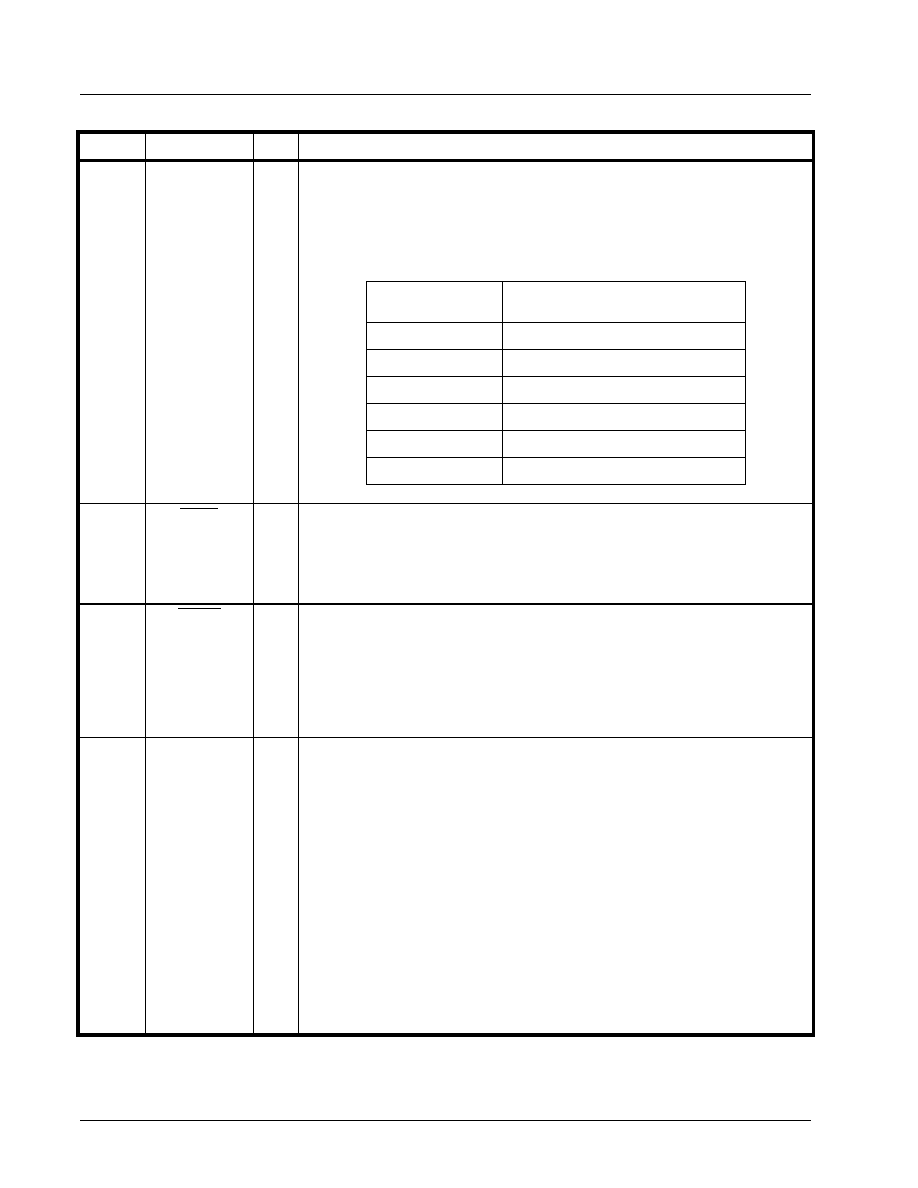
XRT79L71
PRELIMINARY
·Á
·Á
·Á
·Á
REV. P1.0.3
1 - CHANNEL DS3/E3 ATM UNI/PPP COMBO IC
6
J16
J15
J14
PTYPE_0
PTYPE_1
PTYPE_2
I
Microprocessor Type Select input:
These three input pins are used to configure the Microprocessor Interface block to
readily support a wide variety of Microprocessor Interfaces. The relationship
between the settings of these input pins and the corresponding Microprocessor Inter-
face configuration is presented below.
J13
DBEN
I
Bi-directional Data Bus Enable Input pin:
If the Microprocessor Interface is operating in the Intel-I960 Mode, then this input pin
is used to enable the Bi-directional Data Bus.
Setting this input pin "Low" enables the Bi-directional Data bus. Setting this input
"High" tri-states the Bi-directional Data Bus.
B15
BLAST
I
Last Burst Transfer Indicator input pin:
If the Microprocessor Interface is operating in the Intel-I960 Mode, then this input pin
is used to indicate to the Microprocessor Interface block that the current data transfer
is the last data transfer within the current burst operation.
The Microprocessor should assert this input pin by toggling it "Low" in order to
denote that the current READ or WRITE operation within a BURST operation is the
last operation of this BURST operation.
H13
Direct_Ad
I
Direct Address Select pin:
This input pin is used to select the addressing mode for the Microprocessor Interface
block.
Setting this pin "High" will put the Microprocessor Interface block of the XRT79L71
into Direct Addressing Mode.
In Direct Addressing Mode, all 15 address pins (A0 - A14) are used to select the on-
chip Framer/UNI registers and RAM space for READ and WRITE Operations with the
Microprocessor.
N
OTE
: It is recommended to set this pin "High" and access the Microprocessor
Interface block using the Direct Addressing Mode.
Setting this pin "Low" will put the Microprocessor Interface block of the XRT79L71
into Indirect Addressing Mode.
In Indirect Addressing mode, only the lower 8 address pins (A0 - A7) are used to
select the on-chip Framer/UNI registers and RAM space for READ and WRITE Oper-
ations with the Microprocessor. Two microprocessor accesses are needed to READ
or WRITE to the on-chip Framer/UNI registers and RAM space.
PIN DESCRIPTIONS
P
IN
#
N
AME
TYPE
D
ESCRIPTION
P T Y P E [2 :0 ]
010
001
A synchron ous Intel
Intel I960, M otorola M P C 860
011
Intel X 86
100
IB M P ow e r P C
ID T 3051/5 2 (M IP S )
101
A synchron ous M otorola
000
M ic ro p ro c e s s o r In te rfa c e M o d e

·Á
·Á
·Á
·Á
PRELIMINARY
XRT79L71
1 - CHANNEL DS3/E3 ATM UNI/PPP COMBO IC
REV. P1.0.3
7
P
IN
#
N
AME
TYPE
D
ESCRIPTION
TEST AND DIAGNOSTIC
T9
TCK
I
Test Clock input, Boundary Scan Clock input:
N
OTE
: This input pin should be pulled "Low" for normal operation.
P9
TDI
I
Test Data input, Boundary Scan Test Data Input:
N
OTE
: This input pin should be pulled "Low" for normal operation.
N9
TDO
O
Test Data output:
Boundary Scan Test Data Output:
R9
TMS
I
Test Mode Select, Boundary Scan Test Mode Select input pin:
N
OTE
: This input pin should be pulled "Low" for normal operation.
R10
TRST
I
Test Mode Reset, Boundary Scan Mode Reset Input pin:
N
OTE
: This input pin should be pulled "Low" for normal operation.
M15
TESTMODE
***
Factory Test Mode Pin:
Tie this pin to Ground.
P15
ICT
I
In-Circuit Test Input Pin:
For normal operation, the user should pull this pin "High".
N
OTE
: This input pin is internally pulled "High".
P13
P14
AnaIO1
AnaIO2
I/O
Analog Input/Output Test Pin:
These pins should be pulled "Low" for normal operation.
L15
L14
L13
GPI_0
GPI_1
GPI_2
I
General Purpose Input Test Pin:
These pins should be pulled "Low" for normal operation.
K15
K14
K13
GPO_0
GPO_1
GPO_2
O
General Purpose Output Test Pin:
These pins should be left unconnected for normal operation.

XRT79L71
PRELIMINARY
·Á
·Á
·Á
·Á
REV. P1.0.3
1 - CHANNEL DS3/E3 ATM UNI/PPP COMBO IC
8
P
IN
#
N
AME
TYPE
D
ESCRIPTION
GENERAL PURPOSE INPUT AND OUTPUT PINS
T8
DMO
O
Drive Monitor Output Output Pin:
If this input signal is "High", then it means that the drive monitor circuitry within the
XRT79L71 has not detected any bipolar signals at the MTIP and MRING inputs
within the last 128 ± 32 bit periods. If this input signal is "Low", then it means that
bipolar signals are being detected at the MTIP and MRING input pins of the
XRT79L71.
T7
N8
P8
R8
GPIO_0
GPIO_1
GPIO_2
GPIO_3
I/O
General Purpose Input/Output Pins:
Each of these pins can be configured to function as either an input or output pin.
If a given pin is configured to function as an input pin, then the state of this input
pin can be monitored by reading Bit X within the "XXX" Register (Address Loca-
tion = 0xXX, 0xXX).
If a given pin is configured to function as an output pin, then the state of these out-
put pins can be controlled by writing the appropriate value into Bit X within the
"XXX" Register.
P
IN
#
N
AME
TYPE
D
ESCRIPTION
TRANSMIT SYSTEM SIDE INTERFACE PINS
A13
TxAISEn
I
Transmit AIS Pattern Input pin:
This input pin is used to command the Transmit DS3/E3 Framer block to transmit
an AIS pattern to the remote terminal equipment.
Setting this input pin "High" configures the Transmit DS3/E3 Framer block to
transmit an AIS pattern to the remote terminal equipment. Setting this input pin
"Low" configures the Transmit DS3/E3 Framer block to NOT transmit an AIS pat-
tern to the remote terminal equipment.
N
OTE
: For normal operation, or if the user wishes to control the Transmit AIS
function, via Software Control; the user should tie this input pin to GND.
L16
NibbleIntf
I
Nibble Interface Select Input pin:
This input pin is used to configure the Transmit Payload Data Input Interface and
the Receive Payload Data Output Interface blocks to operate in either the Serial
or the Nibble-Parallel Mode.
Setting this input pin "High" configures each of these blocks to operate in
the Nibble-Parallel Mode.
In this mode, the Transmit Payload Data Input Interface block will accept the out-
bound payload data from the local terminal equipment in a nibble-parallel man-
ner via the TxNib[3:0] input pins. Further, the Receive Payload Data Output
Interface block will output inbound payload data to the local terminal equipment
in a nibble-parallel via the RxNib[3:0] output pins.
Setting this input pin "Low" configures each of these blocks to operate in
the Serial Mode.
In this mode, the Transmit Payload Data Input Interface block will accept the out-
bound payload data from the local terminal equipment in a serial manner via the
TxSer input pin. Further, the Receive Payload Data Output Interface block will
output the inbound payload data to the local terminal equipment in a serial man-
ner, via the RxSer output pin.
N
OTE
: This input pin is only active if the XRT79L71 has been configured to
operate in the Clear-Channel Framer Mode.

·Á
·Á
·Á
·Á
PRELIMINARY
XRT79L71
1 - CHANNEL DS3/E3 ATM UNI/PPP COMBO IC
REV. P1.0.3
9
B10
TxFrame
O
Transmit End of DS3/E3 Frame Indicator:
This output pin is pulse "High" for one DS3 or E3 clock period, when the Transmit
Section of the XRT79L71 is processing the last bit of a given DS3 or E3 frame.
The implications of this output pin, for each mode of operation, are described
below.
ATM UNI/PPP/High-Speed HDLC Controller Mode:
This output pin serves as an end-of-frame indication to the local terminal equip-
ment.
Clear-Channel Framer Mode:
If the XRT79L71 is configured to operate in the Clear-Channel Framer mode,
then this output pin serves to alert the Local Terminal Equipment that it needs to
begin transmission of a new DS3 or E3 frame. Hence, the Local Terminal Equip-
ment uses this output signal to maintain Framing Alignment with the XRT79L71.
A11
TxFrameRef
I
Transmit DS3/E3 Framer - Framing Alignment Input pin:
If the the Transmit Section of the XRT79L71 is configured to operate in the Local-
Timing/Frame-Slave Mode, then the Transmit DS3/E3 Framer block will use this
input signal as the Framing Reference.
When the XRT79L71 is configured to operate in this mode any rising edge at this
input pin will cause the Transmit DS3/E3 Framer block to begin its creation of a
new DS3 or E3 frame. Consequently, the user must supply a clock signal that is
equivalent to the DS3 or E3 frame rates to this input pin. Further, it is imperative
that this clock signal be synchronized with the 44.736MHz or 34.368MHz clock
signal applied to the TxInClk input pin.
N
OTE
: This input pin should be tied to GND if it is not to be used as the Transmit
DS3/E3 Framer - Framing Reference input signal.
C10
TxInClk
I
Transmit DS3/E3 Framer Block - Timing Reference Signal:
If the Transmit Section of the XRT79L71 is configured to operate in the Local-
Timing Mode, then it will use this signal as the Timing Reference. If the
XRT79L71 is being operating in the DS3 Mode, then the user is expected to
apply a high-quality 44.736MHz clock signal to this input pin. Likewise, if the
XRT79L71 is being operated in the E3 Mode, then the user is expected to apply
a high-quality 34.368MHz clock signal to this input pin.
Note for Clear-Channel Framer Operation:
If the user is operating the XRT79L71 in the Clear-Channel Framer mode, then
the user should design the local terminal equipment circuitry, such that outbound
DS3 or E3 data will be output, upon the falling edge of TxInClk. The Transmit
Payload Data Input Interface within the Transmit Section of the XRT79L71 will
sample the data, applied to the TxSer input pin, upon the rising edge of TxInClk.
N
OTE
: This input pin should be tied to GND if the XRT79L71 is configured to
operate in the Loop-Timing Mode.
P
IN
#
N
AME
TYPE
D
ESCRIPTION

XRT79L71
PRELIMINARY
·Á
·Á
·Á
·Á
REV. P1.0.3
1 - CHANNEL DS3/E3 ATM UNI/PPP COMBO IC
10
C11
TxOH/
TxHDLCDat_5
I
Transmit Overhead Data Input/Transmit HDLC Controller Data Bit 5 input
pin:
The function of This input pin depends upon whether or not the XRT79L71 has
been configured to operate in the High-Speed HDLC Controller Mode.
Non-High Speed HDLC Controller Mode - TxOH:
The Transmit Overhead Data Input Interface accepts overhead via this input pin,
and insert this data into the overhead bit positions within the outbound DS3 or E3
frames. If the TxOHIns input pin is pulled "High", then the Transmit Overhead
Data Input Interface will sample the overhead data, via this input pin, upon the
falling edge of the TxOHClk output signal.
Conversely, if the TxOHIns input pin is NOT pulled "High", then the Transmit
Overhead Data Input Interface block will be inactive and will not accept any over-
head data via the TxOH input pin.
High Speed HDLC Controller Mode - TxHDLCDat_5:
If the XRT79L71 is configured to operate in the High-Speed HDLC Controller
mode, then the local terminal equipment will be provided with a byte-wide Trans-
mit HDLC Controller byte-wide input interface. This input pin will function as Bit 5
within this byte wide interface.
Data, residing on the Transmit HDLC Controller byte wide input interface, will be
sampled upon the rising edge of the TxHDLCClk output signal.
D10
TxOHIns/
TxHDLCDat_4
I
Transmit Overhead Data Insert Input/Transmit HDLC Controller Data Bit 4
input pin:
The function of this input pin depends upon whether or not the XRT79L71 has
been configured to operate in the High-Speed HDLC Controller Mode.
Non-High Speed HDLC Controller Mode - TxOHIns:
This input pin is used to either enable or disable the Transmit Overhead Data
Input Interface block. If the Transmit Overhead Data Input Interface block is
enabled, then it will accept overhead data from the local terminal equipment via
the TxOH input pin; and insert this data into the overhead bit positions within the
outbound DS3 or E3 data stream.
Conversely, if the Transmit Overhead Data Input Interface block is disabled, then
it will NOT accept overhead data from the local terminal equipment.Pulling this
input pin "High" enables the Transmit Overhead Data Input Interface block. Pull-
ing this input pin "Low" disables the Transmit Overhead Data Input Interface
block.
High-Speed HDLC Controller Mode - TxHDLCDat_4:
If the XRT79L71 is configured to operate in the High-Speed HDLC Controller
mode, then the local terminal equipment will be provided with a byte-wide Trans-
mit HDLC Controller byte-wide input interface. This input pin will function as Bit 4
within this byte wide interface.
Data, residing on the Transmit HDLC Controller byte wide input interface, will be
sampled upon the rising edge of the TxHDLCClk output signal.
B12
TxOHClk
O
Transmit Overhead Clock Output:
This output pin functions as the Transmit Overhead Data Input Interface clock
signal. If the user enables the Transmit Overhead Data Input Interface block by
asserting the TxOHIns input pin, then the Transmit Overhead Data Input Inter-
face block will sample and latch the data residing on the TxOH input pin upon the
falling edge of this signal.
N
OTE
: The Transmit Overhead Data Input Interface block is disabled if the user
has configured the XRT79L71 to operate in the High-Speed HDLC
Controller Mode.
P
IN
#
N
AME
TYPE
D
ESCRIPTION

·Á
·Á
·Á
·Á
PRELIMINARY
XRT79L71
1 - CHANNEL DS3/E3 ATM UNI/PPP COMBO IC
REV. P1.0.3
11
B11
TxOHFrame/
TxHDLCClk
O
Transmit Overhead Framing Pulse/Transmit HDLC Controller Clock Output
pin:
The function of this output pin depends upon whether or not the XRT79L71 has
been configured to operate in the High-Speed HDLC Controller Mode.
Non-High-Speed HDLC Controller Mode - TxOHFrame:
This output pin pulses high for one TxOHClk period coincident with the instant
the Transmit Overhead Data Input Interface would be accepting the first over-
head bit within an outbound DS3 or E3 frame.
High Speed HDLC Controller Mode - TxHDLCClk:
This output pin functions as the demand clock output signal for the Transmit
HDLC Controller byte-wide input interface. This clock signal is ultimately derived
from either the TxInClk or the RxOutClk signal. Hence, the frequency of this
clock signal is nominally one-eight of that of the TxInClk or the RxOutClk signals.
The Transmit HDLC Controller block will sample the contents of the Transmit
HDLC Controller byte-wide input interface, upon the rising edge of this clock out-
put signal. Therefore, the local terminal equipment should be designed to output
data onto the TxHDLCDat[7:0] bus upon the falling edge of this clock output sig-
nal.
A12
TxOHEnable/
TxHDLCDat_7
I/O
Transmit Overhead Enable Output indicator/Transmit HDLC Controller Data
Bit 7 Input:
The function of this input pin depends upon whether or not the XRT79L71 is con-
figured to operate in the High Speed HDLC Controller Mode.
Non-High Speed HDLC Controller Mode - TxOHEnable:
The XRT79L71 will assert this output pin, for one TxInClk period, just prior to the
instant that the Transmit Overhead Data Input Interface will be sampling and pro-
cessing an overhead bit.
If the local terminal equipment intends to insert its own value for an overhead bit,
into the outbound DS3 or E3 data stream, then it is expected to sample the state
of this signal, upon the falling edge of TxInClk. Upon sampling the TxOHEnable
signal "High", the local terminal equipment should;
(1) place the desired value of the overhead bit onto the TxOH input pin and
(2) assert the TxOHIns input pin.
The Transmit Overhead Data Input Interface block will sample and latch the data
on the TxOH signal, upon the rising edge of the very next TxInClk input signal.
High-Speed HDLC Controller Mode - TxHDLCDat_7:
If the XRT79L71 is configured to operate in the High-Speed HDLC Controller
mode, then the local terminal equipment will be provided with a byte-wide Trans-
mit HDLC Controller byte-wide input interface. This input pin will function as Bit 7
(the MSB) within this byte wide interface.
Data, residing on the Transmit HDLC Controller byte wide input interface, will be
sampled upon the rising edge of the TxHDLCClk output signal.
P
IN
#
N
AME
TYPE
D
ESCRIPTION

XRT79L71
PRELIMINARY
·Á
·Á
·Á
·Á
REV. P1.0.3
1 - CHANNEL DS3/E3 ATM UNI/PPP COMBO IC
12
C9
TxSer
TxPOH
SendMSG
I
Transmit Payload Data Serial Input/Transmit PLCP Path Overhead Input/
Send HDLC Message Request Input:
The function of this input pin depends upon whether the XRT79L71 is configured
to operate in the Clear-Channel Framer Mode, the High-Speed HDLC Controller
Mode or in the ATM/PLCP Mode.
Clear-Channel Framer Mode - TxSer:
If the XRT79L71 is configured to operate in the Clear-Channel Framer mode,
then this input pin functions as the Transmit Payload Data Serial Input pin. In this
case, the local terminal equipment is expected to apply all outbound data which
is intended to be carried via the DS3 or E3 payload bits to this input pin.
The Transmit Payload Data Input Interface will sample the data, residing at the
TxSer input pin, upon the rising edge of TxInClk.
ATM/PLCP Mode - TxPOH:
If the XRT79L71 is configured to operate in the ATM Mode, and if within the ATM
Mode, the chip is also configured to operate in the PLCP Mode, then this input
pin functions as the Transmit PLCP Path Overhead Input Pin. In this mode, the
user can externally insert desired path overhead byte values into the outbound
PLCP frames.
The Transmit PLCP Path Overhead Input Pin (and Port) become active whenever
the user asserts the TxPOHIns input pin by pulling it "High". In this case, the
data, residing upon the TxPOH input pin will be sampled upon the rising edge of
the TxPOHClk signal.
N
OTE
: This input pin is inactive if the XRT79L71 is configured to operate in the
Direct-Mapped ATM Mode.
High-Speed HDLC Controller Mode - SendMSG:
If the XRT79L71 is configured to operate in the High-Speed HDLC Controller
Mode, then this input pin functions as the Transmit HDLC Controller Input Inter-
face enable input pin.
If the user asserts this input pin by pulling it "High" then the Transmit HDLC Con-
troller Input Interface will proceed to latch the data, residing on the TxHDL-
CDat[7:0] input pins, upon each rising edge of the TxHDLCClk signal. All data
that is latched into the Transmit HDLC Controller Input Interface for the duration
that the SendMSG input pin is "High" will be encapsulated into an HDLC frame
and ultimately transported via the payload bits of the outbound DS3 or E3 data
stream.
If the user pulling this input pin "Low", then the Transmit HDLC Controller Input
Interface will cease latching the data, residing on the TxHDLCDat[7:0] bus.
N
OTE
: This input pin is inactive if the XRT79L71 has been configured to operate
in the PPP Mode.
B3
TxPOHClk
O
Transmit PLCP Frame POH Byte Insertion Clock:
This pin, along with the TxPOH and the TxPOHMSB input pins, function as the
Transmit PLCP Frame POH Byte serial input port. This output pin functions as a
clock output signal that is be used to sample the user's POH data at the TxPOH
input pin. This output pin is always active, independent of the state of the TxPO-
HIns pin.
N
OTE
: This pin is only active if the XRT79L71 has been configured to operate in
the ATM/PLCP Mode.
P
IN
#
N
AME
TYPE
D
ESCRIPTION

·Á
·Á
·Á
·Á
PRELIMINARY
XRT79L71
1 - CHANNEL DS3/E3 ATM UNI/PPP COMBO IC
REV. P1.0.3
13
B9
TxOHInd/
TxPFrame/
TxHDLCDat_6/
I/O
Transmit Overhead Data Indicator Output/Transmit PLCP Frame Boundary
Indicator Output/Transmit HDLC Controller Data Bit 6 input pin:
The function of these input/output pins depends upon whether the XRT79L71
has been configured to operate in the Clear-Channel Framer Mode, the ATM/
PLCP Mode or the High-Speed HDLC Mode.
Clear-Channel Framer Mode - TxOHInd:
In the Clear-Channel Framer Mode, this output pin functions as the transmit over-
head data indicator for the local terminal equipment. This output pin is pulsed
"High" for one DS3 or E3 bit period in order to indicate to the local terminal
equipment that the Transmit Section of the Framer is going to be processing an
overhead bit, upon the next rising edge of TxInClk., and will NOT latch the data
that is applied to the TxSer input pin. Therefore, when the local terminal equip-
ment samples the TxOHInd output pin "High", then it must not apply the next
payload bit to TxSer input pin. This output pin serves as a warning that this par-
ticular payload bit is going to be ignored by the Transmit Section of the Framer,
and will not be inserted into payload bits, within the outbound DS3 or E3 data
stream.
ATM/PLCP Mode - TxPFrame:
If the XRT79L71 is configured to operate in the ATM UNI/PLCP Mode, then this
output pin will denote the boundaries of outbound PLCP frames, as they are
being processed by the Transmit PLCP Processor block. This output pulses
"High" when the last nibble of a given PLCP frame is being routed to the Transmit
DS3/E3 Framer block.
This output pin is inactive if the XRT79L71 is operating in the Direct-Mapped
ATM Mode.
High-Speed HDLC Controller Mode - TxHDLCDat_6:
If the XRT79L71 is configured to operate in the High-Speed HDLC Controller
mode, then the local terminal equipment will be provided with a byte-wide Trans-
mit HDLC Controller byte-wide input interface. This input pin will function as Bit 6
within this byte wide interface.
Data, residing on the Transmit HDLC Controller byte wide input interface, will be
sampled upon the rising edge of the TxHDLCClk output signal.
P
IN
#
N
AME
TYPE
D
ESCRIPTION

XRT79L71
PRELIMINARY
·Á
·Á
·Á
·Á
REV. P1.0.3
1 - CHANNEL DS3/E3 ATM UNI/PPP COMBO IC
14
D9
TxNibClk/
TxGFCMSB/
SendFCS
I/O
Transmit Nibble Clock Output pin/Transmit GFC Byte - MSB Indicator Out-
put/Send FCS Value Request Input:
The function of this input/output pin depends upon whether the XRT79L71 is
configured to operate in the Clear-Channel Framer Mode, the High-Speed HDLC
Controller Mode or in the ATM Mode.
Clear-Channel Framer Mode - TxNibClk:
When operating in the Nibble-Parallel Mode the XRT79L71 will derive this clock
signal from either the TxInClk or the RxLineClk signal depending upon whether
the chip is operating in the Local-Timing or Loop-Timing Mode.
The user is advised to configure the Terminal Equipment to output the outbound
payload data to the XRT79L71 onto the TxNib_[3:0] input pins, upon the rising
edge of this clock signal. The Transmit Payload Data Input Interface block will
sample the data, residing on the TxNib_[3:0] line, upon the falling edge this clock
signal.
N
OTES
:
1.
For DS3 applications, the XRT79L71 will output 1176 clock pulses to
the local terminal equipment for each outbound DS3 frame.
2.
For E3, ITU-T G.832 applications, the XRT79L71 will output 1074 clock
pulses to the local terminal equipment for each outbound E3 frame.
3.
For E3, ITU-T G.751 applications, the XRT79L71 will output 384 clock
pulses to the local terminal equipment for each outbound E3 frame.
ATM Mode - TxGFCMSB:
This signal, along with TxGFC and TxGFCClk combine to function as the Trans-
mit GFC Nibble Field serial input port. This output signal will pulse "High" when
the MSB (most significant bit) of the GFC nibble for a given outbound cell is
expected at the TxGFC input pin.
High-Speed HDLC Controller Mode - SendFCS:
The local terminal equipment is expected to control both this input pin, along with
the SendMSG input pin, during the construction and transmission of each out-
bound HDLC frame.
This input pin is used to command the Transmit HDLC Controller block to com-
pute and insert the computed FCS (Frame-Check Sequence) value into the
back-end of the outbound HDLC frame, as a trailer.
If the user has configured the Transmit HDLC Controller block to compute and
insert a CRC-16 value into the outbound HDLC frame, then the local terminal
equipment is expected to hold this input pin "High" for two periods of TxHDL-
CClk.Conversely, if the user has configured the Transmit HDLC Controller block
to compute and insert a CRC-32 value into the outbound HDLC frame, then the
local terminal equipment is expected to hold this input pin "High" for four (4) peri-
ods of TxHDLCClk.
N
OTES
:
1.
This input/output pin is inactive if the XRT79L71 has been configured to
operate in the PPP Mode.
2.
This input/output pin is inactive if the XRT79L71 has been configured to
operate in the Clear-Channel Framer/Serial mode.
P
IN
#
N
AME
TYPE
D
ESCRIPTION

·Á
·Á
·Á
·Á
PRELIMINARY
XRT79L71
1 - CHANNEL DS3/E3 ATM UNI/PPP COMBO IC
REV. P1.0.3
15
C2
TxGFCClk
O
Transmit GFC Nibble-Field Serial Input port - Clock Output signal:
This signal, along with TxGFC and TxGFCMSB combine to function as the
Transmit GFC Nibble-field serial input port. This output signal functions as the
demand clock signal for this port. The user will specify the value of the GFC
field, within a given ATM cell, by serially transmitting its four bit-value into the
TxGFC input pin. The Transmit GFC Nibble-Field serial input port will latch the
contents of TxGFC upon the rising edge of this clock signal. Hence, the local ter-
minal equipment should be designed to place its outbound GFC bits on to the
TxGFC line, upon the falling edge of this clock signal.
N
OTE
: This output pin is only active if the XRT79L71 has been configure to
operate in the ATM Mode.
B8
TxNib_3/
TxPOHIns/
TxHDLCDat_3
I
Transmit Nibble Interface - Bit 3/Transmit PLCP Path Overhead Insert
enable/Transmit HDLC Controller Data Bus - Bit 3 input:
The function of this input pin depends upon whether the XRT79L71 is configured
to operate in the Clear-Channel Framer Mode, the High-Speed HDLC Controller
Mode or in the ATM/PLCP Mode.
Clear-Channel Framer Mode - TxNib_3:
If the XRT79L71 is configured to operate in the Nibble-Parallel Mode, then this
input pin will function as the bit 3 (MSB) input to the Transmit Nibble-Parallel input
interface. The Transmit Payload Data Input Interface block will sample this signal
(along with TxNib_0 through TxNib_2) upon the falling edge of TxNibClk.
N
OTE
: This input pin is inactive if the XRT79L71 is configured to operate in the
Serial Mode.
ATM/PLCP Mode - TxPOHIns:
f the XRT79L71 is configured to operate in the ATM Mode, and if (within the ATM
Mode, the chip is also configured to operate in the PLCP Mode), then this input
pin functions as the Transmit PLCP Path Overhead Port - Enable input pin. In
this mode, the user can externally insert desired path overhead byte values into
the outbound PLCP frames.
The Transmit PLCP Path Overhead Input port becomes active whenever the user
asserts this input pin by pulling it "High". Once this occurs, the data, residing
upon the TxPOH input pin will be sampled upon the rising edge of the TxPOHClk
signal.
This input pin is inactive if the XRT79L71 is configured to operate in the Direct-
Mapped ATM Mode.
High-Speed HDLC Controller Mode - TxHDLCDat_3:
If the XRT79L71 is configured to operate in the High-Speed HDLC Controller
mode, then the local terminal equipment will be provided with a byte-wide Trans-
mit HDLC Controller byte-wide input interface. This input pin will function as Bit 3
within this byte wide interface.
Data, residing on the Transmit HDLC Controller byte wide input interface, will be
sampled upon the rising edge of the TxHDLCClk output signal.
P
IN
#
N
AME
TYPE
D
ESCRIPTION

XRT79L71
PRELIMINARY
·Á
·Á
·Á
·Á
REV. P1.0.3
1 - CHANNEL DS3/E3 ATM UNI/PPP COMBO IC
16
C8
TxNib_2/
TxStuff_Ctl/
TxHDLCDat_2
I
Transmit Nibble Input Interface - Bit 2/Transmit PLCP Stuff Control Input/
Transmit HDLC Controller Data Bus - Bit 2 Input:
The function of this input pin depends upon whether the XRT79L71 is configured
to operate in the Clear-Channel Framer Mode, the High-Speed HDLC Controller
Mode, or in the ATM/PLCP Mode.
Clear-Channel Framer Mode - TxNib_2:
If the XRT79L71 is configured to operate in the Nibble-Parallel Mode, then this
input pin will function as the bit 1 input to the Transmit Nibble-Parallel input inter-
face. The Transmit Payload Data Input Interface block will sample this signal
(along with TxNib_0, TxNib_2 and TxNib_3) upon the falling edge of TxNibClk
N
OTE
: This input pin is inactive if the XRT79L71 is configured to operate in the
Serial Mode.
ATM/PLCP Mode - TxStuff_Ctl:
This input pin is used to externally exercise or forego trailer nibble stuffing oppor-
tunities by the Transmit PLCP Processor. PLCP trailer nibble stuff opportunities
occur in periods of three PLCP frames (375 us). The first PLCP frame (first,
within a stuff opportunity period) will have 13 trailer nibbles appended to it. The
second PLCP frame (second within a stuff opportunity period will have 14 trailer
nibbles appended to it. The third PLCP frame (the location of the stuff opportu-
nity) will contain 13 trailer nibbles if this input pin is pulled "Low", and 14 trailer
nibbles if this input pin is pulled "High".
N
OTE
: This input pin is inactive if the XRT79L71 is configured to operate in the
Direct-Mapped ATM Mode.
High-Speed HDLC Controller Mode - TxHDLCDat_2:
If the XRT79L71 is configured to operate in the High-Speed HDLC Controller
mode, then the local terminal equipment will be provided with a byte-wide Trans-
mit HDLC Controller byte-wide input interface. This input pin will function as Bit 1
within this byte wide interface.
Data, residing on the Transmit HDLC Controller byte wide input interface, will be
sampled upon the rising edge of the TxHDLCClk output signal.
P
IN
#
N
AME
TYPE
D
ESCRIPTION

·Á
·Á
·Á
·Á
PRELIMINARY
XRT79L71
1 - CHANNEL DS3/E3 ATM UNI/PPP COMBO IC
REV. P1.0.3
17
D8
TxNib_1/
Tx8KREF/
TxHDLCDat_1
I
Transmit Nibble Input Interface - Bit 1/Transmit PLCP Framing 8kHz Refer-
ence Input/Transmit HDLC Controller Data Bus - Bit 1 Input:
The function of this input pin depends upon whether the XRT79L71 is configured
to operate in the Clear-Channel Framer Mode, the High-Speed HDLC Controller
Mode, or in the ATM/PLCP Mode.
Clear-Channel Framer Mode - TxNib_1:
If the XRT79L71 is configured to operate in the Nibble-Parallel Mode, then this
input pin will function as the bit 1 input to the Transmit Nibble-Parallel input inter-
face. The Transmit Payload Data Input Interface block will sample this signal
(along with TxNib_0, TxNib_2 and TxNib_3) upon the falling edge of TxNibClk.
N
OTE
: This input pin is inactive if the XRT79L71 is configured to operate in the
Serial Mode.
ATM/PLCP Mode - Tx8KREF:
If the XRT79L71 is configured to operate in the ATM/PLCP Mode, then the Trans-
mit PLCP Processor can be configured to synchronize its PLCP frame genera-
tion to this input clock signal. The Transmit PLCP Processor will also use this
input signal to compute the nibble-trailer stuff opportunities.
N
OTE
: This input pin is inactive if the use has configured the XRT79L71 to
operate in the Direct-Mapped ATM Mode.
High-Speed HDLC Controller Mode - TxHDLCDat_1:
If the XRT79L71 is configured to operate in the High-Speed HDLC Controller
mode, then the local terminal equipment will be provided with a byte-wide Trans-
mit HDLC Controller byte-wide input interface. This input pin will function as Bit 1
within this byte wide interface.
Data, residing on the Transmit HDLC Controller byte wide input interface, will be
sampled upon the rising edge of the TxHDLCClk output signal.
A9
TxNib_0/
TxGFC/
TxHDLCDat_0
I
Transmit Nibble Interface - Bit 0/Transmit GFC Input pin/Transmit HDLC
Controller Data Bus - Bit 0 Input:
The function of this input pin depends upon whether the XRT79L71 is configured
to operate in the Clear-Channel Framer Mode, the High Speed HDLC Controller
Mode or in the ATM Mode.
Clear-Channel Framer Mode - TxNib_0:
If the XRT79L71 is configured to operate in the Nibble-Parallel Mode, then this
input pin will function as the bit 0 (LSB) input to the Transmit Nibble-Parallel input
interface. The Transmit Payload Data Input Interface block will sample this signal
(along with TxNib_1 through TxNib_3) upon the falling edge of TxNibClk.
N
OTE
: This input pin is inactive if the XRT79L71 is configured to operate in the
Serial Mode.
ATM Mode - TxGFC:
This signal, along with TxGFCMSB, and TxGFCClk combine to function as the
Transmit GFC Nibble Field serial input port. The user will specify the value of the
GFC field, within a given ATM cell, by serially transmitting its four bit-value into
this input pin. Each of these four bits will be clocked into the port upon the rising
edge of the TxGFCClk output signal.
High-Speed HDLC Controller Mode - TxHDLCDat_0:
If the XRT79L71 is configured to operate in the High-Speed HDLC Controller
mode, then the local terminal equipment will be provided with a byte-wide Trans-
mit HDLC Controller byte-wide input interface. This input pin will function as Bit 0
(the LSB) within this byte wide interface.
Data, residing on the Transmit HDLC Controller byte wide input interface, will be
sampled upon the rising edge of the TxHDLCClk output signal.
P
IN
#
N
AME
TYPE
D
ESCRIPTION

XRT79L71
PRELIMINARY
·Á
·Á
·Á
·Á
REV. P1.0.3
1 - CHANNEL DS3/E3 ATM UNI/PPP COMBO IC
18
A10
TxCellTxed/
TxNibFrame/
ValidFCS
O
Transmit Cell Generator indicator/Transmit Nibble Frame Indicator/Valid
FCS Indicator output:
The function of this output pin depends upon whether the XRT79L71 has been
configured to operate in the ATM Mode, the Clear-Channel Framer Mode or in
the High-Speed HDLC Controller Mode.
ATM Mode - TxCellTxed:
This output pin pulses "High" each time the Transmit Cell Processor transmits a
cell to either the Transmit PLCP Processor or the Transmit DS3/E3 Framer block.
Clear-Channel Framer Mode - TxNibFrame:
This output pin pulses "High" when the last nibble of a given DS3 or E3 frame is
expected at the TxNib[3:0] input pins.
The purpose of this output pin is to alert the local terminal equipment that it
needs to begin the transmission of a new DS3 or E3 frame to the XRT79L71.
N
OTE
: This output pin is not active if the XRT79L71 is configured to operate in
the Serial-Mode.
High-Speed HDLC Controller Mode - ValidFCS:
The combination of the RxIdle and ValidFCS output signals are used to convey
information about data that is being output via the Receive HDLC Controller out-
put Data bus (RxHDLCDat_[7:0]).
If RxIdle = "High":
The Receive HDLC Controller block with drive this output pin "High" anytime the
flag sequence octet (0x7E) is present on the RxHDLCDat[7:0] output data bus.
If RxIdle and ValidFCS are both "High":
The Receive HDLC Controller block has received a complete HDLC frame, and
has determined that the FCS value within this HDLC frame are valid.
If RxIdle is "High" and ValidFCS is "Low":
The Receive HDLC Controller block has received a complete HDLC frame, and
has determined that the FCS value within this HDLC frame is invalid.
If RxIdle is "High" and ValidFCS is "Low":
The Receive HDLC Controller block has received an ABORT sequence.
M2
TxPERR
I
Transmit Error Indicator from Link Layer:
This input signal is used to indicate that the current packet is ABORTED and
must be discarded. This input pin should only be asserted when the last byte (or
word) is be written onto the TxPData[15:0] input pins.
N
OTE
: This input pin is only active if the XRT79L71 has been configured to
operate in the PPP Mode.
N1
TxPEOP
I
Transmit POS-PHY Interface - End of Packet:
The link layer processor toggles this output pin "High" whenever the Link Layer
Processor is writing the last byte (or word) of a given Packet into the TxP-
Data[15:0] data bus.
N
OTES
:
1.
This input pin is only valid when the XRT79L71 is configured to operate
in the PPP Mode.
2.
This input pin is only valid when the Transmit POS-PHY Interface -
Write Enable Input pin (TxPEn) is asserted.
P
IN
#
N
AME
TYPE
D
ESCRIPTION

·Á
·Á
·Á
·Á
PRELIMINARY
XRT79L71
1 - CHANNEL DS3/E3 ATM UNI/PPP COMBO IC
REV. P1.0.3
19
R3
TxUPrty/
TxPPrty
I
Transmit UTOPIA Data Bus - Parity Input/Transmit POS-PHY Interface - Par-
ity Input:
The function of this input pin depends upon whether the XRT79L71 has been
configured to operate in the ATM UNI or PPP Mode.
ATM UNI Mode - TxUPrty:
The ATM Layer processor will apply the parity value of the byte or word which is
being applied to the Transmit UTOPIA Data Bus (e.g., TxUData[7:0] or TxU-
Data[15:0]) inputs of the XRT79L71, respectively.
N
OTE
: This parity value should be computed based upon the odd-parity of the
data applied at the Transmit UTOPIA Data Bus.
The Transmit UTOPIA Interface block within the XRT79L71 will independently
compute an odd-parity value of each byte (or word) that it receives from the ATM
Layer processor and will compare it with the logic level of this input pin.
PPP Mode - TxPPrty:
The Link Layer Processor will apply the parity value of the byte or word which is
being applied to the Transmit POS-PHY Data Bus (e.g., TxPData[7:0] or TxP-
Data[15:0]) inputs of the XRT79L71, respectively.
N
OTE
: This parity value should be computed based upon the odd-parity of the
data applied to the Transmit POS-PHY Data Bus. The Transmit POS-
PHY Interface block within the XRT79L71 will independently compute an
odd-parity value of each byte (or word) that it receives from the Link
Layer processor and will compare it will the logic level of this input pin.
M4
TxUEN/
TxPEN
I
Transmit UTOPIA Interface Block - Write Enable/Transmit POS-PHY Interface -
Write Enable:
The function of this input pin depends upon whether the XRT79L71 has been
configured to operate in the ATM UNI or PPP Mode.
ATM UNI Mode Operation - TxUEN:
This active-low signal, from the ATM Layer processor enables the data on the
Transmit UTOPIA Data Bus to be written into the TxFIFO on the rising edge of
TxUClk. When this signal is asserted, then the contents of the byte or word that
is present, on the Transmit UTOPIA Data Bus, will be latched into the Transmit
UTOPIA Interface block, on the rising edge of TxUClk.
When this signal is negated, then the Transmit UTOPIA Data bus inputs will be
tri-stated.
PPP Mode Operation - TxPEN:
This active-low signal, from the Link Layer processor enables the data on the
Transmit POS-PHY Data Bus to be written into the TxFIFO on the rising edge of
TxPClk. When this signal is asserted, then the contents of the byte or word that
is present, on the Transmit POS-PHY Data Bus, will be latched into the Transmit
POS-PHY Interface block, on the rising edge of TxPClk.
When this signal is negated, then the Transmit POS-PHY Data bus inputs will be
tri-stated.
P
IN
#
N
AME
TYPE
D
ESCRIPTION

XRT79L71
PRELIMINARY
·Á
·Á
·Á
·Á
REV. P1.0.3
1 - CHANNEL DS3/E3 ATM UNI/PPP COMBO IC
20
N3
TxUClav/
TxPPA
O
Transmit UTOPIA Interface - Cell Available Output Pin/Transmit POS-PHY
Interface - Packet Data Available Output pin:
The function of this output pin depends upon whether the XRT79L71 has been
configured to operate in the ATM UNI or PPP Mode.
ATM UNI Mode - TxUClav:
This output pin supports data flow control between the ATM Layer processor and
the Transmit UTOPIA Interface block. This signal is asserted (toggles "High")
when the TxFIFO is capable of receiving at least one more full cell of data from
the ATM Layer processor. This signal is negated, if the TxFIFO is not capable of
receiving one more full cell of data from the ATM Layer processor.
Multi-PHY Operation:
When the UNI chip is operating in the Multi-PHY mode, this signal will be tri-
stated until the TxUClk cycle following the assertion of a valid address on the
Transmit UTOPIA Address bus input pins (e.g., when the contents on the Trans-
mit UTOPIA Address bus pins match that within the Transmit UTOPIA Address
Register. Afterwards, this output pin will behave in accordance with the cell-level
handshake mode.
PPP Mode - TxPPA:
The XRT79L71 will drive this output pin "High" whenever a programmable num-
ber of bytes of empty space is available for writing more packet data into the
TxFIFO.
P3
TxUSoC/
TxPSoP
I
Transmit UTOPIA - Start of Cell Input/Transmit POS-PHY - Start of Packet
Input:
The function of this input signal depends upon whether the XRT79L71 has been
configured to operate in the ATM UNI or in the PPP Mode.
ATM UNI Mode Operation - TxUSoC:
This input pin is driven by the ATM Layer Processor and is used to indicate the
start of an ATM cell that is being transmitted from the ATM Layer Processor. This
input pin must be pulsed "High" whenever the first byte (or word) of a new cell is
present on the Transmit UTOPIA Data Bus (TxUData[15:0]). This input pin must
remain "Low" at all other times.
PPP Mode Operation - TxPSoP/TxPSoC:
If the XRT79L71 has been configured to operate in the Packet-Mode, then this
input pin is pulsed "High" to denote that the first byte (or word) of a given packet
is placed on the TxPData[15:0] input pins.If the XRT79L71 has been configured
to operate in the Cell-Chunk Mode, then this input pin is pulsed "High" to denote
that the first byte of a packet chunk, if placed on the TxPData[15:0] input pins.
N
OTE
: This input pin is only valid if the XRT79L71 has been configured to
operate in the PPP Mode.
P
IN
#
N
AME
TYPE
D
ESCRIPTION

·Á
·Á
·Á
·Á
PRELIMINARY
XRT79L71
1 - CHANNEL DS3/E3 ATM UNI/PPP COMBO IC
REV. P1.0.3
21
L4
TxTSX/
TxPSOF
I
Transmit - Start of Transfer/Transmit - Start of PPP Packet in Chunk Mode:
The function of this input pin depends upon whether the XRT79L71 has been
configured to operate in the Packet Mode or Cell-Chunk Mode.
Packet Mode - TxTSX:
The Link-Layer processor pulses this input pin "High" when an in-band port
address is present on the TxPData[7:0] bus.
When this input pin and TxPEN are both set "High" then the value of TxP-
Data[7:0] is the address value of the TxFIFO to be selected. Subsequent write
operations, into TxPData[15:0] will fill the TxFIFO corresponding to this inband
address.
Chunk Mode - TxPSOF:
The Link Layer processor pulses this input pin "High" in order to indicate that the
first byte (or word) of a given Packet is placed on the TxPData[15:0] pins.
N
OTE
: This input pin is only active if the XRT79L71 has been configured to
operate in the PPP Mode.
P1
TxUClkO/
TxPClkO
O
Transmit UTOPIA Interface Clock/Transmit POS-PHY Interface Clock Out-
put:
This output is derived from an internal PLL.
M1
TxUClk/
TxPClk
I
Transmit UTOPIA Interface Clock/Transmit POS-PHY Interface Clock Input:
The function of this input pin depends upon whether the XRT79L71 has been
configured to operate in the ATM UNI or in the PPP Mode.
ATM UNI Mode - TxUClk:
The Transmit UTOPIA Interface clock is used to latch the data on the Transmit
UTOPIA Data bus, into the Transmit UTOPIA Interface block. This clock signal is
also used as the timing source for circuitry used to process the ATM cell data into
and through the TxFIFO.
During Multi-PHY operation, the data on the Transmit UTOPIA Address bus pins
is sampled on the rising edge of TxUClk.
PPP Mode - TxPClk:
The Transmit POS-PHY Interface clock is used to latch the data on the Transmit
POS-PHY Data bus, into the Transmit POS-PHY Interface block. This clock sig-
nal is also used as the timing source for circuitry used to process the Packet data
into and through the TxFIFO.
T2
T1
R2
R1
P2
TxUAddr_0
TxUAddr_1
TxUAddr_2
TxUAddr_3
TxUAddr_4
I
Transmit UTOPIA Address Bus:
These input pins comprise the Transmit UTOPIA Address Bus input pins. The
Transmit UTOPIA Address Bus is only in use when the XRT79L71 is operating in
the Multi-PHY mode. When the ATM Layer processor wishes to write data to a
particular UNI (PHY-Layer) device, it will provide the address of the intended UNI
on the Transmit UTOPIA Address Bus. The contents of the Transmit UTOPIA
Address Bus input pins are sampled on the rising edge of TxUClk. The UNI will
compare the data on the Transmit UTOPIA Address Bus with the pre-pro-
grammed contents of the TxUT Address Register (Address = 70h). If these two
values are identical and the TxUEN pin is asserted, then the TxUClav pin will be
driven to the appropriate state based upon the TxFIFO fill level for the Cell Level
handshake mode of operation.
P
IN
#
N
AME
TYPE
D
ESCRIPTION

XRT79L71
PRELIMINARY
·Á
·Á
·Á
·Á
REV. P1.0.3
1 - CHANNEL DS3/E3 ATM UNI/PPP COMBO IC
22
M3
TxMod
I
Transmit PPP Data Bus - Modulo Indicator:
This input pin is used to specify the number of valid packet octets are being
placed on the TxPData[15:0] input pins.
The Link Layer Processor is expected to set this input pin "Low" when both bytes
on the TxPData[15:0] data bus is valid packet data. Conversely, the Link Layer
Processor is expected to set this input pin "High" when only the upper octet has
valid packet data.
N
OTES
:
1.
This input pin is only active if the XRT79L71 has been configured to
operate in the PPP Mode.
2.
The Link Layer Processor is expected to set this input pin to the
appropriate state, as each 16-bit word is being written into the
TxPData[15:0] data bus.
T3
P4
R4
T4
N5
P5
R5
T5
N6
P6
N4
R6
T6
N7
P7
R7
TxUData_0/
TxPData_0
TxUData_1/
TxPData_1
TxUData_2/
TxPData_2
TxUData_3/
TxPData_3
TxUData_4/
TxPData_4
TxUData_5/
TxPData_5
TxUData_6/
TxPData_6
TxUData_7/
TxPData_7
TxUData_8/
TxPData_8
TxUData_9/
TxPData_9
TxUData_10/
TxPData_10
TxUData_11/
TxPData_11
TxUData_12/
TxPData_12
TxUData_13/
TxPData_13
TxUData_14/
TxPData_14
TxUData_15/
TxPData_15
I
Transmit UTOPIA Data Bus Inputs/Transmit POS-PHY Data Bus Inputs:
The function of these input pins depends upon whether the XRT79L71 is operat-
ing in the ATM UNI Mode or in the PPP Mode.
ATM UNI Operation - TxUData[15:0]:
These input pins comprise the Transmit UTOPIA Data Bus input pins. When the
ATM Layer Processor wishes to transmit ATM cell data through the XRT72L74
ATM UNI, it must place this data on these pins. The data, on the Transmit UTO-
PIA Data Bus is latched into the Transmit UTOPIA Interface block upon the rising
edge of TxUClk.
PPP Operation - TxPDATA[15:0]
These input pins comprise the Transmit POS-PHY Data Bus input pins. When a
Network Processor wishes to transmit PPP data through the XRT79L71 Framer/
UNI IC, it must place this data on these pins. The data, on the Transmit POS-
PHY Data Bus is latched into the Transmit POS-PHY Interface block upon the ris-
ing edge of TxPClk.
P
IN
#
N
AME
TYPE
D
ESCRIPTION

·Á
·Á
·Á
·Á
PRELIMINARY
XRT79L71
1 - CHANNEL DS3/E3 ATM UNI/PPP COMBO IC
REV. P1.0.3
23
P
IN
#
N
AME
TYPE
D
ESCRIPTION
RECEIVE SYSTEM SIDE INTERFACE PINS
A4
RxAIS/
RxNib_2/
RxHDLCDat_2
O
Receive AIS Pattern Indicator/Receive Nibble Output Interface - Bit 2/
Receive HDLC Controller Data Bus - Bit 2 output pin:
The function of this output pin depends upon whether the XRT79L71 has been
configured to operate in the Clear-Channel Framer/Nibble-Parallel Interface
Mode, the High-Speed HDLC Controller Mode, or in the other modes.
Other Modes - RxAIS:
This output pin is driven "High" whenever the Receive Section of the XRT79L71
has detected and is currently declaring an AIS (Alarm Indicator Signal) condi-
tion.
Clear-Channel Framer/Nibble-Parallel Interface Mode - RxNib_2:
If the XRT79L71 is configured to operate in the Nibble-Parallel Mode, then this
output pin will function as the bit 2 output from the Receive Nibble-Parallel out-
put interface. The Receive Payload Data Output Interface block will output this
signal (along with RxNib_0, RxNib_1, and RxNib_3) upon the rising edge of the
RxClk output signal.
High-Speed HDLC Controller Mode - RxHDLCDat_2:
This output pin along with RxHDLCDat_[7:3] and RxHDLCDat_[1:0] functions
as the Receive HDLC Controller byte wide output data bus. The Receive HDLC
Controller will output the contents of all HDLC frames via this output data bus,
upon the rising edge of the RxHDLCClk output signal. Hence, the user's local
terminal equipment should be designed/configured to sample this data upon the
falling edge of the RxHDLCClk output clock signal.
B4
RxRED/
RxNib_3/
RxHDLCDat_3
O
Receive Section Red Alarm Indicator/Receive Nibble Interface Output pin -
Bit 3/Receive HDLC Controller Data Bus output pin - Bit 3:
The function of this output pin depends upon whether the XRT79L71 has been
configured to operate in the Clear-Channel Framer/Nibble-Parallel Mode, the
High-Speed HDLC Controller Mode, or in some other mode.
Clear-Channel Framer/Nibble-Parallel Mode - RxNib_3:
The XRT79L71 will output Received data from the remote terminal equipment
to the local terminal equipment via this pin, along with RxNib_0 through
RxNib_2. This particular output pin functions as the LSB. The data at this pin is
updated on the rising edge of the RxClk output signal. Hence, the user's local
terminal equipment should sample this signal upon the falling edge of RxClk.
High-Speed HDLC Controller Mode - RxHDLCDat_3:
This output pin along with RxHDLCDat_[7:4] and RxHDLCDat_[2:0] functions
as the Receive HDLC Controller byte wide output data bus. The Receive HDLC
Controller will output the contents of all HDLC frames via this output data bus,
upon the rising edge of the RxHDLCClk output signal. Hence, the user's local
terminal equipment should be designed/configured to sample this data upon the
falling edge of the RxHDLCClk output clock signal.
Other Modes - RxRED:
The Framer/UNI asserts this output pin to denote that one of the following
events has been detected by the Receive DS3/E3 Framer block:
∑
LOS - Loss of Signal Condition
∑
OOF - Out of Frame Condition
∑
AIS - Alarm Indication Signal Detection

XRT79L71
PRELIMINARY
·Á
·Á
·Á
·Á
REV. P1.0.3
1 - CHANNEL DS3/E3 ATM UNI/PPP COMBO IC
24
D6
RxOOF/
RxNib_1/
RxHDLCDat_1
O
Receive Out of Frame Indicator/Receive Nibble Interface Output pin - Bit 1/
Receive HDLC Controller Data Bus Output pin - Bit 1:
The function of this output pin depends upon whether the XRT79L71 has been
configured to operate in the Clear-Channel Framer/Nibble-Parallel Mode or the
High-Speed HDLC Controller Mode.
Clear-Channel Framer/Nibble-Parallel Mode - RxNib_1:
The XRT79L71 will output Received data from the remote terminal equipment
to the local terminal equipment via this pin, along with RxNib_0, RxNib_2 and
RxNib_3: This particular output pin functions as the LSB. The data at this pin is
updated on the rising edge of the RxClk output signal. Hence, the user's local
terminal equipment should sample this signal upon the falling edge of RxClk.
High-Speed HDLC Controller Mode - RxHDLCDat_1:
This output pin along with RxHDLCDat_[7:2] and RxHDLCDat_0 functions as
the Receive HDLC Controller byte wide output data bus. The Receive HDLC
Controller will output the contents of all HDLC frames via this output data bus,
upon the rising edge of the RxHDLCClk output signal. Hence, the user's local
terminal equipment should be designed/configured to sample this data upon the
falling edge of the RxHDLCClk output clock signal.
All other Modes - RxOOF:
The UNI Receive DS3 Framer will assert this output signal whenever it has
declared an Out of Frame (OOF) condition with the incoming DS3 frames. This
signal is negated when the framer correctly locates the F- and M-bits and
regains synchronization with the DS3 frame.
B5
RxLCD/
RxOutClk/
RxHDLCDat_7
O
Receive Loss of Cell Delineation indicator/Receive Output Clock signal/
Receive HDLC Controller Data Bus - Bit 7 Output:
The function of output pin depends upon whether the XRT79L71 has been con-
figured to operate in the ATM, Clear-Channel Framer or High Speed HDLC Con-
troller Mode.
ATM Mode - RxLCD:
This active-high output pin will be asserted whenever the Receive Cell Proces-
sor has experienced a Loss of Cell Delineation. This pin will return "Low" once
the Receive Cell Processor has regained Cell Delineation.
Clear-Channel Framer Mode - RxOutClk:
This clock signal functions as the Transmit Payload Data Input Interface clock
source, if the XRT79L71 has been configured to operate in the loop-timing
mode.
In this mode, the local terminal equipment is expected to input data to the TxSer
input pin, upon the rising edge of this clock signal. The XRT79L71 will use the
rising edge of this signal to sample the data on the TxSer input.
High-Speed HDLC Controller Mode - RxHDLCDat_7:
This output pin along with RxHDLCDat_[6:0] functions as the Receive HDLC
Controller byte wide output data bus. This particular output pin functions as the
MSB (Most Significant Bit) of the Receive HDLC Controller byte wide data bus.
The Receive HDLC Controller will output the contents of all HDLC frames via
this output data bus, upon the rising edge of the RxHDLCClk output signal.
Hence, the user's local terminal equipment should be designed/configured to
sample this data upon the falling edge of the RxHDLCClk output clock signal.
P
IN
#
N
AME
TYPE
D
ESCRIPTION

·Á
·Á
·Á
·Á
PRELIMINARY
XRT79L71
1 - CHANNEL DS3/E3 ATM UNI/PPP COMBO IC
REV. P1.0.3
25
D7
RxLOS
O
Framer/UNI - Loss of Signal Output Indicator:
This pin is asserted when the Receive Section of the XRT79L71 encounters
180 consecutive 0's (for DS3 applications) or 32 consecutive 0's (for E3 applica-
tions) via the RxPOS and RxNEG pins. This pin will be negated once the
Receive DS3/E3 Framer has detected at least 60 "1s" out of 180 consecutive
bits (for DS3 applications) or has detected at least four consecutive 32 bit
strings of data that contain at least 8 "1s" in the receive path.
B2
RxPRED
O
Receiver Red Alarm Indicator - Receive PLCP Processor:
The Framer/UNI asserts this output pin to denote that one of the following
events has been detected by the Receive PLCP Processor:
∑
OOF - Out of Frame Condition
∑
LOF - Loss of Frame Condition
N
OTE
: This output pin is only valid if the XRT79L71 has been configured to
operate in the ATM/PLCP Mode.
D5
RxPOOF
O
Receive PLCP Out of Frame Indicator:
The Receive PLCP Processor will assert this pin, when it declares an Out of
Frame condition. This output will be negated when the Receive PLCP Proces-
sor reaches the In Frame Condition.
N
OTE
: This output pin is only valid if the XRT79L71 has been configured to
operate in the ATM/PLCP Mode.
A2
RxPLOF
O
Receive PLCP - Loss of Frame Output Indicator:
The Receive PLCP Processor will assert this pin, when it declares a Loss of
Frame condition. This output will be negated when the Receive PLCP Proces-
sor reaches the In Frame Condition.
N
OTE
: This output pin is only active is the XRT79L71 has been configured to
operate in the ATM/PLCP Mode.
C5
RxNib_0/
RxHDLCDat_0
O
Receive Nibble Interface Output pin - Bit 0/Receive HDLC Controller Data
Bus output pin - Bit 0:
The function of this output pin depends upon whether the XRT79L71 has been
configured to operate in the Clear-Channel/Nibble-Parallel Mode, the High-
Speed HDLC Controller Mode, or in some other mode.
Clear-Channel/Nibble-Parallel Mode - RxNib_0:
The XRT79L71 will output Received data from the remote terminal equipment
to the local terminal equipment via this pin, along with RxNib_1 through
RxNib_3. This particular output pin functions as the LSB.
The data at this pin is updated on the rising edge of the RxClk output signal.
Hence, the user's local terminal equipment should sample this signal upon the
falling edge of RxClk.
High-Speed HDLC Controller Mode - RxHDLCDat_0:
This output pin along with RxHDLCDat_[7:1] functions as the Receive HDLC
Controller byte wide output data bus. This particular output pin functions as the
LSB (Least Significant Bit) of the Receive HDLC Controller byte wide data bus.
The Receive HDLC Controller will output the contents of all HDLC frames via
this output data bus, upon the rising edge of the RxHDLCClk output signal.
Hence, the user's local terminal equipment should be designed/configured to
sample this data upon the falling edge of the RxHDLCClk output clock signal.
N
OTE
: This output pin is only active if the XRT79L71 is configured to operate in
the Clear-Channel/Nibble-Parallel Mode or in the High-Speed HDLC
Controller Mode. This output is inactive for all remaining modes.
P
IN
#
N
AME
TYPE
D
ESCRIPTION

XRT79L71
PRELIMINARY
·Á
·Á
·Á
·Á
REV. P1.0.3
1 - CHANNEL DS3/E3 ATM UNI/PPP COMBO IC
26
B7
RxOHEnable/
RxHDLCDat_5
O
Receive Overhead Data Output Interface - Enable Output/Receive HDLC
Controller Data Bus - Bit 5 output:
The function of this output pin depends upon whether the XRT79L71 has been
configured to operate in the Clear-Channel Framer Mode or in the High-Speed
HDLC Controller Mode.
Clear-Channel Framer Mode - RxOHEnable:
The XRT79L71 will assert this output signal for one RxOHClk period when it is
safe for the local terminal equipment to sample the data on the RxOH output
pin.
High-Speed HDLC Controller Mode - RxHDLCDat_5:
This output pin along with RxHDLCDat_[4:0], RxHDLCDat_6 and
RxHDLCDat_7 functions as the Receive HDLC Controller byte wide output data
bus. The Receive HDLC Controller will output the contents of all HDLC frames
via this output data bus, upon the rising edge of the RxHDLCClk output signal.
Hence, the user's local terminal equipment should be designed/configured to
sample this data upon the falling edge of the RxHDLCClk output clock signal.
C7
RxOH/
RxHDLCDat_6
O
Receive Overhead Data Output Interface - output/Receive HDLC Controller
Data Bus - Bit 6 output:
The function of this output pin depends upon whether the XRT79L71 has been
configured to operate in the Clear-Channel Framer mode or in the High-Speed
HDLC Controller Mode.
Clear-Channel Framer Mode - RxOH:
All overhead bits, which are received via the Receive Section of the XRT79L71
will be output via this output pin, upon the rising edge of RxOHClk.
High-Speed HDLC Controller Mode - RxHDLCDat_6:
This output pin along with RxHDLCDat_[5:0] and RxHDLCDat_7 functions as
the Receive HDLC Controller byte wide output data bus. The Receive HDLC
Controller will output the contents of all HDLC frames via this output data bus,
upon the rising edge of the RxHDLCClk output signal. Hence, the user's local
terminal equipment should be designed/configured to sample this data upon the
falling edge of the RxHDLCClk output clock signal.
A7
RxOHClk/
RxHDLCClk
O
Receive Overhead Data Output Interface - clock/Receive HDLC Controller -
Clock output:
The function of this output pin depends upon whether the XRT79L71 has been
configured to operate in the Clear-Channel Framer mode or in the High-Speed
HDLC Controller Mode.
Clear-Channel Framer Mode - RxOHClk:
The XRT79L71 will output the overhead bits within the incoming DS3 or E3
frames via the RxOH output pin, upon the falling edge of this clock signal.
As a consequence, the user's local terminal equipment should use the rising
edge of this clock signal to sample the data on both the RxOH and RxOHFrame
output pins.
N
OTE
: This clock signal is always active.
High-Speed HDLC Controller Mode - RxHDLCClk:
This output pin functions as the Receive HDLC Controller Data bus clock out-
put. The Receive HDLC Controller block outputs the contents of all received
HDLC frames via the Receive HDLC Controller Data bus (RxHDLCDat_[7:0])
upon the rising edge of this clock signal. Hence, the user's local terminal equip-
ment should be designed/configured to sample this data upon the falling edge
of this clock signal.
P
IN
#
N
AME
TYPE
D
ESCRIPTION

·Á
·Á
·Á
·Á
PRELIMINARY
XRT79L71
1 - CHANNEL DS3/E3 ATM UNI/PPP COMBO IC
REV. P1.0.3
27
A8
RxOHFrame/
RxHDLCDat_4
O
Receive Overhead Data Interface - Framing Pulse indicator/Receive HDLC
Controller Data Bus - Bit 4 output:
The function of this output pins depends upon whether the XRT79L71 has been
configured to operate in the Clear-Channel Framer Mode or in the High-Speed
HDLC Controller Mode.
Clear-Channel Framer Mode - RxOHFrame:
This output pin pulses "High" whenever the Receive Overhead Data Output
Interface block outputs the first overhead bit of a new DS3 or E3 frame.
High-Speed HDLC Controller Mode - RxHDLCDat_4:
This output pin along with RxHDLCDat_[3:0] and RxHDLCDat_[7:5] functions
as the Receive HDLC Controller byte wide output data bus. The Receive HDLC
Controller will output the contents of all HDLC frames via this output data bus,
upon the rising edge of the RxHDLCClk output signal. Hence, the user's local
terminal equipment should be designed/configured to sample this data upon the
falling edge of the RxHDLCClk output clock signal.
B6
RxFrame
0
Receive Boundary of DS3 or E3 Frame Output indicator:
The function of this output pin depends upon whether or not the XRT79L71 is
operating in the Clear-Channel Framer/Nibble-Parallel Mode.
Clear-Channel Framer/Nibble-Parallel Mode:
The Receive Section of the XRT79L71 will pulse this output pin "High" for one
nibble period, when the Receive Payload Data Output interface block is driving
the very first nibble of a given DS3 or E3 frame, on the RxNib[3:0] output pins.
Clear-Channel Framer/Serial Mode:
The Receive Section of the XRT79L71 will pulse this output pin "High" for one
bit period, when the Receive Payload Data Output interface block is driving the
very first bit of a given DS3 or E3 frame, on the RxSer output pin.
All Other Modes:
The Receive Section of the XRT79L71 will pulse this output pin "High" when the
Receive DS3/E3 Framer block is processing the first bit within a new DS3 or E3
frame.
D4
RxCellRxed
O
Receive Cell Processor - Cell Received Indicator:
This output pin pulses "High" each time the Receive Cell Processor receives a
new cell from the Receive PLCP Processor or the Receive DS3/E3 Framer
block.
N
OTE
: This output pin is only active if the XRT79L71 has been configured to
operate in the ATM UNI Mode.
P
IN
#
N
AME
TYPE
D
ESCRIPTION

XRT79L71
PRELIMINARY
·Á
·Á
·Á
·Á
REV. P1.0.3
1 - CHANNEL DS3/E3 ATM UNI/PPP COMBO IC
28
A5
RxPOH/
RxSer
O
Receive PLCP Path Overhead Output pin/Receive Serial Output pin:
The function of this output depends upon whether the XRT79L71 has been con-
figured to operate in the ATM/PLCP Mode or in the Clear-Channel Framer
Mode.
ATM/PLCP Mode - RxPOH:
This output pin along with the RxPOHClk, RxPOHFrame and RxPOHIns pins
comprise the Receive PLCP Frame POH Byte serial output port. For each
PLCP frame, that is received by the Receive PLCP Processor, this serial output
port will output the contents of all 12 POH (Path Overhead) bytes. The data that
is output via this pin, is updated on the rising edge of the RxPOHClk output
clock signal. The RxPOHFrame pin will pulse "High" whenever the first bit of the
Z6 byte is being output via this output pin.
Clear-Channel Framer Mode - RxSer:
If the XRT79L71 is configured to operate in the Clear-Channel Framer/Serial
Mode, then the chip will output all received data, via this output pin. This output
signal will be updated upon the rising edge of RxClk.
N
OTE
: The user should either configure the XRT79L71 to operate in the
Gapped-Clock Mode, or validate the sampling of each bit from the
RxSer output with the state of RxOHInd' output pin, in order to prevent
the local terminal equipment from sampling overhead bits.
This output pin is only active if the XRT79L71 has been configured to operate in
the ATM/PLCP or the Clear-Channel Framer/Serial Mode. This pin is inactive
for all remaining modes of operation.
P
IN
#
N
AME
TYPE
D
ESCRIPTION

·Á
·Á
·Á
·Á
PRELIMINARY
XRT79L71
1 - CHANNEL DS3/E3 ATM UNI/PPP COMBO IC
REV. P1.0.3
29
A6
RxPOH_Clk/
RxClk/
RxNibClk
O
Receive PLCP Path Overhead Serial Port Clock output/Receive Nibble-Par-
allel Output port clock/Receive Serial Clock output:
The function of this output pin depends upon whether the XRT79L71 has been
configured to operate in the ATM/PLCP Mode or the Clear-Channel Framer
Mode.
ATM/PLCP Mode - RxPOH_Clk:
This output clock pin along with RxPOH, RxPOHFrame and RxPOHIns pins
comprise the Receive PLCP Frame POH Byte serial output port. All POH (Path
Overhead) data that is output via the RxPOH output pin is updated on the rising
edge of this clock signal.
N
OTE
: This output signal is inactive if the XRT79L71 has been configured to
operate in the Direct-Mapped ATM Mode.
Clear-Channel Framer Mode - RxClk:
This output pin is active whenever the XRT79L71 has been configured to oper-
ate in either the Serial or Nibble Parallel Mode, as is described below.Clear-
Channel Framer/Serial Mode - RxClkIn this serial mode, this output is a
44.736MHz clock output signal (for DS3 applications) or 34.368MHz clock out-
put signal (for E3 applications). The Receive Payload Data Output Interface will
update the data via the RxSer output pin, upon the rising edge of this clock sig-
nal.
The user is advised to design (or configure) the local terminal equipment to
sample the RxSer data, upon the falling edge of this clock signal.
Clear-Channel Framer/Nibble-Parallel Mode - RxNibClk:
In the Nibble-Parallel Mode, the XRT79L71 will derive this clock signal from the
RxLineClk signal. The XRT79L71 will pulse this clock signal 1176 times for
each inbound DS3 frame or 1074 times for each inbound E3/ITU-T G.832 frame
or 384 times for each inbound E3/ITU-T G.751 frame. The Receive Payload
Data Output Interface block will update the data on the RxNib[3:0] output upon
the falling edge of this clock signal.
The user is advised to design (or configure) the local terminal equipment to
sample the data on the RxNib[3:0] output pins, upon the rising edge of this clock
signal.
C4
RxPOHFrame
O
Receive PLCP Frame POH Serial Output Port - Frame Indicator:
This output pin along with the RxPOH RxPOHClk and RxPOHIns pins comprise
the Receive PLCP Frame POH Byte serial output port. This output pin provides
framing information to external circuitry receiving and processing this POH
(Path Overhead) data, by pulsing "High" whenever the first bit of the Z6 byte is
being output via the RxPOH output pin. This pin is "Low" at all other times dur-
ing this PLCP POH Framing cycle.
N
OTE
: This output pin is only active if the XRT79L71 has been configured to
operate in the ATM/PLCP Modes.
P
IN
#
N
AME
TYPE
D
ESCRIPTION

XRT79L71
PRELIMINARY
·Á
·Á
·Á
·Á
REV. P1.0.3
1 - CHANNEL DS3/E3 ATM UNI/PPP COMBO IC
30
C6
RxPFrame/
RxOHInd
O
Receive PLCP Frame Indicator/Receive Overhead Indicator Output:
The function of this output pin depends upon whether the XRT79L71 has been
configured to operate in the ATM/PLCP, the Clear-Channel Framer/Serial or the
Clear-Channel Framer/Nibble-Parallel Modes.
ATM/PLCP Mode - RxPFrame:
This output pin pulses "High" when the Receive PLCP Processor is receiving
the last bit of a PLCP frame.
N
OTE
: This output pin is inactive if the XRT79L71 is configured to operate in the
Direct-Mapped ATM Mode.
Clear-Channel Framer/Serial Mode - RxOHInd:
This output pin pulses "High" for one bit-period whenever an overhead bit is
being output via the RxSer output pin, by the Receive Payload Data Output
Interface block.
N
OTE
: If the user configures the XRT79L71 to operate in the Gapped-Clock
Mode, then this output pin will provide a demand clock to the local
terminal equipment. In the Gapped-Clock Mode, this output pin will only
provide a clock pulse, whenever a payload bit is being output via the
RxSer output pin. This output pin will NOT generate a clock pulse,
whenever an overhead is being output via the RxSer output pin.
Clear-Channel Framer/Nibble-Parallel - RxOHInd:
This output pin pulse "High" for one nibble-period whenever an overhead nibble
is being output via the RxNib[3:0] output pins by the Receive Payload Data Out-
put Interface block.
N
OTE
: The purpose of this output pin is to alert the local terminal equipment
that an overhead bit (or nibble) is being output via the RxSer or
RxNib[3:0] output pins and that this data should be ignored.
C3
RxGFC/
RxIdle
O
Receive GFC Nibble Field - Output Pin/Receive Idle Sequence Indicator:
The function of this output pin depends upon whether the XRT79L71 is operat-
ing in the ATM Mode or in the High-Speed HDLC Controller Mode.
ATM Mode - RxGFC:
This pin, along with the RxGFCClk and the RxGFCMSB pins form the Receive
GFC Nibble-Field serial output port. This pin will serially output the contents of
the GFC Nibble field of each cell that is processed via the Receive Cell Proces-
sor. This data is serially clocked out of this pin on the rising edge of the RxGFC-
Clk signal. The MSB of each GFC value is designated by a pulse at the
RxGFCMSB output pin.
High-Speed HDLC Controller Mode - RxIdle:
The combination of the RxIdle and ValidFCS output signals are used to convey
information about data that is being output via the Receive HDLC Controller out-
put Data bus (RxHDLCDat_[7:0]).
If RxIdle = "High":
The Receive HDLC Controller block will drive this output pin "High" anytime the
flag sequence octet (0x7E) is present on the RxHDLCDat[7:0] output data bus.
If RxIdle and ValidFCS are both "High":
The Receive HDLC Controller block has received a complete HDLC frame, and
has determined that the FCS value within this HDLC frame are valid.
If RxIdle is "High" and ValidFCS is "Low":
The Receive HDLC Controller block has received a complete HDLC frame, and
has determined that the FCS value within this HDLC frame is invalid.
If RxIdle is "High" and ValidFCS is "Low":
The Receive HDLC Controller block has received an ABORT sequence.
P
IN
#
N
AME
TYPE
D
ESCRIPTION

·Á
·Á
·Á
·Á
PRELIMINARY
XRT79L71
1 - CHANNEL DS3/E3 ATM UNI/PPP COMBO IC
REV. P1.0.3
31
A1
RxGFCClk
O
Received GFC Nibble Serial Output Port Clock Signal:
This output pin functions as a part of the Receive GFC Nibble-Field Serial Out-
put Port, also consisting of the RxGFC and RxGFCMSB pins. This pin provides
a clock pulse which allows external circuitry to latch in the GFC Nibble-Data via
the RxGFC output pin.
N
OTE
: This output pin is only active if the XRT79L71 is operating in the ATM
UNI Mode.
B1
RxGFCMSB
O
Receive GFC Nibble Field - MSB Indicator:
This output pin functions as a part of the Receive GFC Nibble Field Serial Out-
put port which also consists of the RxGFC and RxGFCClk pins. This pin pulses
"High" the instant that the MSB (Most Significant Bit) of a GFC Nibble is being
output on the RxGFC pin.
N
OTE
: This output pin is only active if the XRT79L71 is operating in the ATM
UNI Mode.
H1
RxUClav/RxPPA
O
Receive UTOPIA - Cell Available/Receive POS-PHY Interface - Packet
Available:
The function of this output pin depends upon whether the XRT79L71 has been
configured to operate in the ATM UNI or PPP Mode.
ATM UNI Mode - RxUClav:
The Receive UTOPIA Interface block will assert this output pin in order to indi-
cate that the Rx FIFO has some ATM cell data that needs to be read by the ATM
Layer Processor. This signal is asserted if the RxFIFO contains at least one full
cell of data. This signal toggle "Low" if the RxFIFO is depleted of data, or if it
contains less than one full cell of data.
Multi-PHY Operation:
When the UNI chip is operating in the Multi-PHY mode, this signal will be tri-
stated until the RxClk cycle following the assertion of a valid address on the
Receive UTOPIA Address bus input pins (e.g., if the contents on the Receive
UTOPIA Address bus pins match that with the Receive UTOPIA Address Regis-
ter. Afterwards, this output pin will behave in accordance with the cell-level
handshake mode.
PPP Mode - RxPPA:
The XRT79L71 will drive this output pin "High" whenever a programmable num-
ber of bytes are available to be read from the RxFIFO.
K2
RxUClkO/
RxPClkO
O
Receive UTOPIA Interface Clock/Receive POS-PHY Interface Clock Out-
put:
This clock output signal is derived from an internal PLL.
L3
RxUClk/
RxPClk
I
Receive UTOPIA Interface Clock Input/Receive POS-PHY Interface Clock
Input:
The function of this input pin depends upon whether the XRT79L71 is operating
in the ATM UNI or PPP Mode.
ATM UNI Mode - RxUClk:
The byte (or word) data, on the Receive UTOPIA Data bus (RxUData[15:0]) is
updated on the rising edge of this signal. The Receive UTOPIA Interface can
be clocked at rates up to 50 MHz.
PPP Mode - RxPClk:
This byte (or word) data, on the Receive POS-PHY Data Bus (RxPData[15:0]) is
updated on the rising edge of this signal. The Receive POS-PHY Interface can
be clocked at rates up to 50MHz.
P
IN
#
N
AME
TYPE
D
ESCRIPTION

XRT79L71
PRELIMINARY
·Á
·Á
·Á
·Á
REV. P1.0.3
1 - CHANNEL DS3/E3 ATM UNI/PPP COMBO IC
32
L2
RxPERR
O
Receive POS-PHY Interface - Error Indicator:
This output pin indicates whether or not the Receive POS-PHY Interface has
detected an error in the inbound PPP Packet.
This output pin toggles "High" if the Receive Section of the XRT79L71 detects
an FCS Error, an ABORT sequence or a Runt Packet.
N
OTE
: This output pin is only valid if the XRT79L71 has been configured to
operate in the PPP Mode.
K4
RxTSX/
RxPSOF
O
Receive - Start of Transfer/Receive - Start of PPP Packet in Chunk Mode:
The function of this output pin depends upon whether the XRT79L71 has been
configured to operate in the Packet Mode or Cell-Chunk Mode.
Packet Mode - RxTSX:
The XRT79L71 pulses this output pin "High" when an inband port address is
present on the RxPData[7:0] bus.
When this output pin is "High", the value of RxPData[7:0] is the address value of
the RxFIFO to be selected. Subsequent read operations, from RxPData[15:0]
will be from the RxFIFO corresponding to this inband address.
Chunk Mode - RxPSOF:
The XRT79L71 pulses this output pin "High" in order to indicate that the first
byte (or word) of a given Packet is placed on the RxPData[15:0] pins.
N
OTE
: This output pin is only active if the XRT79L71 has been configured to
operate in the PPP Mode.
H4
RxUEN/
RxPEN
I
Receive UTOPIA Interface - Output Enable/Receive POS-PHY Interface -
Output Enable:
The function of this output pin depends upon whether the XRT79L71 has been
configured to operate in the ATM UNI or PPP mode.
ATM UNI Mode - RxUEN:
This active-low input signal is used to control the drivers of the Receive UTOPIA
Data Bus. When this signal is "High" (negated) then the Receive UTOPIA Data
Bus is tri-stated. When this signal is asserted, then the contents of the byte or
word that is at the front of the RxFIFO will be popped and placed on the Receive
UTOPIA Data bus on the very next rising edge of RxUClk.
PPP Mode - RxPEN:
This active-low input signal is used to control the drivers of the Receive POS-
PHY Data Bus. When this signal is "High" (negated) then the Receive POS-
PHY Data Bus is tri-stated. When this signal is asserted, then the contents of
the byte or word that is at the front of the RxFIFO will be popped and placed on
the Receive POS-PHY Data bus on the very next rising edge of RxPClk.
H2
RxUSoC/
RxPSOP
O
Receive UTOPIA Interface - Start of Cell Indicator/Receive POS-PHY Inter-
face - Start of Packet Indicator:
The function of this output pin depends upon whether the XRT79L71 has been
configured to operate in the ATM UNI or in the PPP Mode.
ATM UNI Mode - RxUSoC:
This output pin allows the ATM Layer Processor to determine the boundaries of
the ATM cells that are output via the Receive UTOPIA Data bus. The Receive
UTOPIA Interface block will assert this signal when the first byte (or word) of a
new cell is present on the Receive UTOPIA Data Bus; RxUData[15:0].
PPP Mode - RxPSOP:
This output pin allows the Link Layer Processor to determine the boundaries of
the PPP packets that are output via the Receive POS-PHY Data Bus. The
Receive POS-PHY Interface block will assert this signal when the first byte (or
word) of a new packet is present on the Receive POS-PHY Data Bus, RxP-
Data[15:0].
P
IN
#
N
AME
TYPE
D
ESCRIPTION

·Á
·Á
·Á
·Á
PRELIMINARY
XRT79L71
1 - CHANNEL DS3/E3 ATM UNI/PPP COMBO IC
REV. P1.0.3
33
H3
RxUPrty/
RxPPrty
O
Receive UTOPIA Interface - Parity Output pin/Receive POS-PHY Interface -
Parity Output:
The function of this output pin depends upon whether the XRT79L71 has been
configured to operate in the ATM UNI or the PPP Modes.
ATM UNI Mode - RxUPrty:
The Receive UTOPIA interface block will compute the odd-parity value of each
byte (or word) that it will place in the Receive UTOPIA Data Bus. This odd-par-
ity value will be output on this pin, while the corresponding byte (or word) is
present on the Receive UTOPIA Data Bus
PPP Mode - RxPPrty:
The Receive POS-PHY Interface block will compute the odd-parity value of
each byte (or word) that it will place in the Receive POS-PHY Data Bus. This
odd parity value will be output on this pin, which the corresponding byte (or
word) is present on the Receive POS-PHY Data Bus.
K3
RxPEOP
O
Receive POS-PHY Interface - End of Packet:
The XRT79L71 drives this output pin "High" whenever the last byte of a given
Packet is being output via the RxPData[15:0] data bus.
N
OTES
:
1.
This output pin is only valid when the XRT79L71 is configured to
operate in the PPP Mode.
2.
This output pin is only valid when the Receive POS-PHY Interface -
Read Enable Output pin.
N2
RxPDVAL
O
Receive POS-PHY Interface Signal Valid Indicator:
This output signal indicates whether or not the Receive POS-PHY Interface sig-
nals (e.g., PRData[15:0], RxPSOP, RxPEOP, RxPPrty, RxPERR) are valid.
This output pin will be driven "High", when these signals are valid. Conversely,
this output pin will be driven "Low" when these signals are NOT valid.
N
OTE
: This output pin is only active if the XRT79L71 has been configured to
operate in the PPP Mode.
J1
J2
J3
J4
K1
RxAddr_0
RxAddr_1
RxAddr_2
RxAddr_3
RxAddr_4
I
Receive UTOPIA Address Bus input MSB:
These input pins functions as the Receive UTOPIA Address bus inputs. These
input pins are only active when the Framer/UNI device is operating in the ATM
UNI Mode. The Receive UTOPIA Address Bus input is sampled on the rising
edge of the RxClk signal. The contents of this address bus are compared with
the value stored in the Rx UT Address Register (Address = 0x6C). If these two
values match, then the UNI will inform the ATM Layer Processor on whether or
not it has any new ATM cells to be read from the RxFIFO by driving the RxClav
output to the appropriate level. If these two address values do not match, then
the UNI will not respond to the ATM Layer Processor and will keep its RxClav
output signal tri-stated.
P
IN
#
N
AME
TYPE
D
ESCRIPTION

XRT79L71
PRELIMINARY
·Á
·Á
·Á
·Á
REV. P1.0.3
1 - CHANNEL DS3/E3 ATM UNI/PPP COMBO IC
34
G2
G1
F1
G3
F2
E1
G4
F3
E2
D1
F4
E3
D2
C1
E4
D3
RxUData_0/
RxPData_0
RxUData_1/
RxPData_1
RxUData_2/
RxPData_2
RxUData_3/
RxPData_3
RxUData_4/
RxPData_4
RxUData_5/
RxPData_5
RxUData_6/
RxPData_6
RxUData_7/
RxPData_7
RxUData_8/
RxPData_8
RxUData_9/
RxPData_9
RxUData_10/
RxPData_10
RxUData_11/
RxPData_11
RxUData_12/
RxPData_12
RxUData_13/
RxPData_13
RxUData_14/
RxPData_14
RxUData_15/
RxPData_15
O
Receive UTOPIA Data Bus Input/Receive POS-PHY Data Bus Output pins:
The function of these output pins depends upon whether the XRT79L71 has
been configured to operate in the ATM UNI or in the PPP Mode.
ATM UNI Mode - RxUData[15:0]:
These output pins function as the Receive UTOPIA Data Bus. ATM cell data
that has been received from the Remote Terminal Equipment is output on the
Receive UTOPIA Data Bus, where it can be read and processed by the ATM
Layer Processor.
PPP Mode - RxPData[15:0]:
These output pins function as the Receive POS-PHY Data Bus output pins.
PPP Packet data that has been received from the Remote Terminal Equipment
is output on the Receive POS-PHY Data Bus, where it can be reads and pro-
cessed by the Link Layer Processor.
L1
RxMod
O
Receive PPP Data Bus - Modulus Indicator:
The XRT79L71 will indicate the number of valid packet octets that are being
read out of the RxPData[15:0] output pins.
The XRT79L71 will drive this output pin "Low" when both bytes of the RxP-
Data[15:0] data bus consists of valid packet data.
Conversely, the XRT79L71 will drive this output pin "High" when only the upper
byte of the RxPData[15:0] data bus consists of valid packet data.
The Link Layer Processor is expected to validate all packet data that it reads out
of the RxPData[15:0] output pins by also reading the state of this output pin.
N
OTE
: This output pin is only active if the XRT79L71 has been configured to
operate in the PPP Mode.
P
IN
#
N
AME
TYPE
D
ESCRIPTION

·Á
·Á
·Á
·Á
PRELIMINARY
XRT79L71
1 - CHANNEL DS3/E3 ATM UNI/PPP COMBO IC
REV. P1.0.3
35
P
IN
#
N
AME
TYPE
D
ESCRIPTION
TRANSMIT LINE SIDE SIGNALS
R15
TxON
I
Transmit Driver ON - Channel n:
This input pin is used to either enable or disable the Transmit Output Driver of the
XRT79L71.
"Low" - Disables the XRT79L71 Transmit Output Driver. In this setting, the TTIP
and TRING output pins will be tri-stated.
"High" - Enables the XRT79L71 Transmit Output Driver. In this setting, the TTIP
and TRING output pins will be enabled.
N
OTES
:
1.
Whenever the transmitters are turned off , the TTIP and TRING output
pins will be tri-stated.
2.
These pins are internally pulled high.
P16
M16
DS3CLK
E3CLK
I
Transmit Clock Input:
These input pins function as the timing source for the XRT79L71 Transmit Section.
N
OTE
: The user is expected to supply a 44.736MHz ± 20ppm clock signal (for
DS3 applications) or a 34.368MHz ± 20 ppm clock signal (for E3
applications).
T11
TTIP
O
Transmit Output - Positive Polarity Signal:
This output pin, along with the TRING output pin, function as the Transmit DS3/E3
output signal drivers for the XRT79L71.
The user is expected to connect this signal and the TRING output signal to a 1:1
transformer.
Whenever the Transmit Section of the XRT79L71 generates and transmits a posi-
tive-polarity pulse onto the line, this output pin will be pulsed to a "higher-voltage"
than the TRING output pin.
Conversely, whenever the Transmit Section of the XRT79L71 generates and trans-
mit a negative-polarity pulse onto the line, this output pin will be pulsed to a "lower-
voltage" than the TRING output pin.
N
OTE
: This output pin will be tri-stated whenever the user sets the TxON input pin
(or bit-field) to "0".
T10
TRING
O
Transmit Output - Negative Polarity Signal:
This output pin along with the TTIP output pin, functions as the Transmit DS3/E3
output signal drivers for the XRT79L71.
The user is expected to connect this signal and the TTIP output signal to a 1:1
transformer.
Whenever the Transmit Section of the XRT79L71 generates and transmits a posi-
tive-polarity pulse onto the line, this output pin will be pulsed to a "lower-voltage"
than the TTIP output pin.
Conversely, whenever the Transmit Section of the XRT79L71 generates and trans-
mit a negative-polarity pulse onto the line, this output pin will be pulsed to a
"higher-voltage" than the TTIP output pin.
N
OTE
: This output pin will be tri-stated whenever the user sets the TxON input pin
(or bit-field) to "0".

XRT79L71
PRELIMINARY
·Á
·Á
·Á
·Á
REV. P1.0.3
1 - CHANNEL DS3/E3 ATM UNI/PPP COMBO IC
36
P10
MTIP
I
Transmit Drive Monitor Input pin - Positive Polarity Input:
This input pin along with MRING functions as the Transmit Drive Monitor Output
(DMO) input monitoring pins.
If the user wishes to (1) monitor the Transmit Output line signal and (2) to perform
this monitoring externally, then the user MUST connect this particular pin to the
TTIP output pin via a 274 ohm series resistor. Similarly, the user MUST also con-
nect the MRING input pin to the TRING output pin via a 274 ohm series resistor.
The MTIP and MRING input pins will continuously monitor the Transmit Output line
signal via the TTIP and TRING output pins for bipolar activity. If these pins do not
detect any bipolar activity for 128 bit periods, then the Transmit Drive Monitor cir-
cuit will drive the DMO output pin "High" in order to denote a possible fault condi-
tion in the Transmit Output Line signal path.
N
OTES
:
1.
This input pin is inactive if the user choose to internally monitor the
Transmit Output line signal.
2.
Internal Monitoring is only available as an option if the user is operating
the XRT79L71 in the Host Mode.
P11
MRING
I
Transmit Drive Monitor Input pin - Negative Polarity Input:
This input pin along with MTIP functions as the Transmit Drive Monitor Output
(DMO) input monitoring pins.
If the user wishes to (1) monitor the Transmit Output line signal and (2) to perform
this monitoring externally, then the user MUST connect this particular input pin to
the TRING output pin via a 274 ohm series resistor. Similarly, the user MUST also
connect the MTIP input pin to the TTIP output pin via a 274 ohm series resistor.
The MTIP and MRING input pins will continuously monitor the Transmit Output line
signal via the TTIP and TRING output pins for bipolar activity. If these pins do not
detect any bipolar activity for 128 bit periods, then the Transmit Drive Monitor cir-
cuit will drive the DMO output pin "High" in order to denote a possible fault condi-
tion in the Transmit Output Line signal path.
N
OTES
:
1.
This input pin is inactive if the user chooses to internally monitor the
Transmit Output line signal.
2.
Internal Monitoring is only available as an option if the user is operating
the XRT79L71 in the Host Mode.
P
IN
#
N
AME
TYPE
D
ESCRIPTION
RECEIVE LINE SIDE SIGNALS
R14
RTIP
I
Receive Input - Positive Polarity Signal:
This input pin, along with the RRING input pin, functions as the Receive DS3/E3
Line input signal receiver of the XRT79L71.
The user is expected to connect this signal and the RRING input signal to a 1:1
transformer.
Whenever the RTIP/RRING input pins are receiving a positive-polarity pulse
within the incoming DS3 or E3 line signal, this input pin will be pulsed to a
"higher-voltage" than the RRING input pin.
Conversely, whenever the RTIP/RRING input pins are receiving a negative-polar-
ity pulse within the incoming DS3 or E3 line signal, this input pin will be pulsed to
a "lower-voltage" than the RRING input pin.
P
IN
#
N
AME
TYPE
D
ESCRIPTION

·Á
·Á
·Á
·Á
PRELIMINARY
XRT79L71
1 - CHANNEL DS3/E3 ATM UNI/PPP COMBO IC
REV. P1.0.3
37
R13
RRING
I
Receive Input - Negative Polarity Signal:
This input pin, along the RTIP input pin, functions as the Receive DS3/E3 Line
input signal receiver for the XRT79L71.
The user is expected to connect this signal and the RTIP input signal to a 1:1
transformer.
Whenever the RTIP/RRING input pins are receiving a positive-polarity pulse
within the incoming DS3 or E3 line signal, then this input pin will be pulsed to a
"lower-voltage" than the RTIP input pin.
Conversely, whenever the RTIP/RRING input pins are receiving a negative-polar-
ity pulse within the incoming DS3 or E3 line signal, then this input pin will be
pulsed to a "higher-voltage" than the RTIP input pin.
K16
CLKOUT
O
Receive (Recovered) Clock Output:
This output pin functions as the Receive or recovered clock signal. All Receive
(or recovered) data will output via the RTIP and RRING outputs upon the user-
selectable edge of this clock signal.
P
IN
#
N
AME
TYPE
D
ESCRIPTION
VDD PINS
G7
G8
G9
G10
K7
K8
K9
K10
H14
N14
3.3V Power Supply Pins
R16
CLKVDD
3.3V Clock Power Supply Pin
T16
JAAVDD
3.3V Jitter Attenuator Analog Power Supply Pin
N13
OVDD
3.3V Output Power Supply Pin
R12
REFAVDD
3.3V Reference Analog Power Supply Pin
T13
RXAVDD
3.3V Receive Analog Power Supply Pin
N11
TXDVDD
3.3V Transmit Digital Power Supply Pin
T12
TXAVDD
3.3V Transmit Analog Power Supply Pin
P
IN
#
N
AME
TYPE
D
ESCRIPTION

XRT79L71
PRELIMINARY
·Á
·Á
·Á
·Á
REV. P1.0.3
1 - CHANNEL DS3/E3 ATM UNI/PPP COMBO IC
38
P
IN
#
N
AME
TYPE
D
ESCRIPTION
GND PINS
H7
H8
H9
H10
J7
J8
J9
J10
H15
N15
Ground Pins
N16
CLKGND
3.3V Clock Ground Pin
T15
JAAGND
3.3V Jitter Attenuator Analog Ground Pin
M13
OGND
3.3V Output Ground Pin
P12
REFAGND
3.3V Reference Analog Ground Pin
T14
RXAGND
3.3V Receive Analog Ground Pin
N10
TXDGND
3.3V Transmit Digital Ground Pin
N12
TXAGND
3.3V Transmit Analog Ground Pin
P
IN
#
N
AME
TYPE
D
ESCRIPTION
NOT CONNECTED PINS
R11
No Connect Pin

·Á
·Á
·Á
·Á
PRELIMINARY
XRT79L71
1 - CHANNEL DS3/E3 ATM UNI/PPP COMBO IC
REV. P1.0.3
39
ELECTRICAL CHARACTERISTICS
AC ELECTRICAL CHARACTERISTIC INFORMATION
MICROPROCESSOR INTERFACE TIMING FOR REVISION A SILICON
MICROPROCESSOR INTERFACE TIMING - ASYNCHRONOUS INTEL MODE
N
OTE
: The values for "t0" through "t7", in this figure can be found in Table 3.
T
ABLE
2: DC ELECTRICAL CHARACTERISTICSS
A
PPLIES
TO
ALL
TTL-L
EVEL
I
NPUT
AND
CMOS L
EVEL
O
UTPUT
PINS
- A
MBIENT
T
EMPERATURE
= 25∞C
S
YMBOL
P
ARAMETER
T
EST
C
ONDITION
M
IN
M
AX
U
NITS
VDDQ
I/O Supply Voltage
3.135
3.465
V
VIH
High-Level Input Voltage
VOUT ≥ VOH(min)
2.0
VDD + 0.3
V
VIL
Low-Level Input Voltage
VOUT < VOL (max)
-0.3
0.3*VDD
V
VOH
High-Level Output Voltage
VDD = MIN
VIN = VIH
IOH = -2mA
1.9
V
VOL
Low-Level Output Voltage
VDD = MIN
VIN = VIL
IOL = 2mA
0.6
V
II
Input Current
VDD = MAX
VIN = VDD or GND
±15
mA
F
IGURE
2. A
SYNCHRONUS
M
ODE
1 - I
NTEL
TYPE
P
ROGRAMMED
I/O T
IMING
(W
RITE
C
YCLE
)
A
h
M d 1 I
l T
Addres
Data
t5
CS
ALE AS
A[14:0]
D[7:0]
RD_DS
WR R/W
t
0
t
1
t
3
t
4
t
2
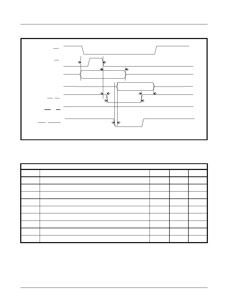
XRT79L71
PRELIMINARY
·Á
·Á
·Á
·Á
REV. P1.0.3
1 - CHANNEL DS3/E3 ATM UNI/PPP COMBO IC
40
N
OTE
: The values for "t0" through "t7", in this figure can be found in Table 3.
F
IGURE
3. A
SYNCHRONUS
M
ODE
1 - I
NTEL
TYPE
P
ROGRAMMED
I/O T
IMING
(R
EAD
C
YCLE
)
T
ABLE
3: T
IMING
I
NFORMATION
FOR
THE
M
ICROPROCESSOR
I
NTERFACE
,
WHEN
CONFIGURED
TO
OPERATE
IN
THE
I
NTEL
A
SYNCHRONOUS
M
ODE
Test Conditions: TA = 25∞C, VCC = 3.3V±5% and 2.5V±5%, unless otherwise specified.
T
IMING
D
ESCRIPTION
M
IN
.
T
YP
.
M
AX
.
t0
Address setup time to pALE low
4
-
-
t1
Address hold time from pALE low
4
-
-
t2
pRD_L, pWR_L pulse width
320
-
-
t3
Data setup time to pWR_L low
0
-
-
t4
Data hold time from pWR_L high
0
-
-
t5
pALE low to pRD_L, pWR_L low
5
-
-
t6
Data invalid from pRD_L high
4
-
-
t7
Data valid from pRDY_L low
-
-
0
t8
pRDY inactive from pRD_L inactive
3
9
Address
Data
CS
ALE_AS
A[14:0]
D[7:0]
RD_DS
WR_R/W
RDY_DTACK
t
2
t
7
t
6
t
1
t
0
t
5
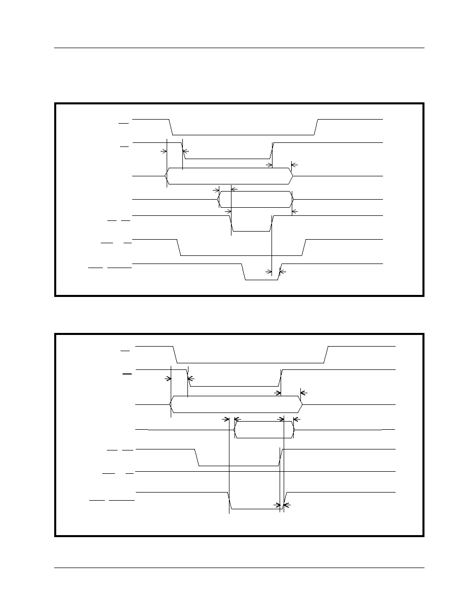
·Á
·Á
·Á
·Á
PRELIMINARY
XRT79L71
1 - CHANNEL DS3/E3 ATM UNI/PPP COMBO IC
REV. P1.0.3
41
MICROPROCESSOR INTERFACE TIMING - ASYNCHRONOUS MOTOROLA (68K)
MODE
N
OTE
: The values for "t0" through "t7" can be found in Table 4.
N
OTE
: The values for "t0" through "t7" can be found in Table 4.
F
IGURE
4. A
SYNCHRONUS
M
ODE
2 - M
OTOROLA
68K P
ROGRAMMED
I/O T
IMING
(W
RITE
C
YCLE
)
F
IGURE
5. A
SYNCHRONUS
M
ODE
2 - M
OTOROLA
68 P
ROGRAMMED
I/O T
IMING
(R
EAD
C
YCLE
)
Address
Data
t
0
CS
ALE_AS
A[14:0]
D[7:0]
RD_DS
WR_R/W
RDY_DTACK
t
2
t
3
t
4
t
1
Data
CS
ALE_AS
A[14:0]
D[7:0]
RD_DS
WR_R/W
RDY DTACK
t
6
t
7
Address
t
0
t
1
t
5

XRT79L71
PRELIMINARY
·Á
·Á
·Á
·Á
REV. P1.0.3
1 - CHANNEL DS3/E3 ATM UNI/PPP COMBO IC
42
MICROPROCESSOR INTERFACE TIMING - POWER PC 403 SYNCHRONOUS MODE
N
OTE
: The value for "t0" through "t12" can be found in Table 5.
T
ABLE
4: T
IMING
I
NFORMATION
FOR
THE
M
ICROPROCESSOR
I
NTERFACE
WHEN
CONFIGURED
TO
OPERATE
IN
THE
M
OTOROLA
(68K) A
SYNCHRONOUS
M
ODE
Test Conditions: TA = 25∞C, VCC = 3.3V±5% and 2.5V±5%, unless otherwise specified.
T
IMING
D
ESCRIPTION
M
IN
.
T
YP
.
M
AX
t0
Address setup time to pALE low
6
-
-
t1
Address hold time to pALE high
6
-
-
t2
Data setup time to pDS_L low
0
-
-
t3
Data hold time to pDS_L low
160
-
-
t4
pDS_L high to pRDY_L high (Write Cycle)
-
-
16
t5
pRDY_L low to Data valid
-
-
15
t6
pDS_L high to pRDY_L high (Read Cycle)
-
-
16
t7
pRDY_L high to Data invalid
3
-
-
F
IGURE
6. S
YNCHRONOUS
M
ODE
3 - IBM P
OWER
PC 403 I
NTERFACE
TIMING
(W
RITE
C
YCLE
)
pCLK
pCS_L
pA[14:0
]
pD[7:0]
pRdy
pRW_L
pOE_L
t0
t1
t2
t3
t4
t5
t6
t7
Address
Data
pWE_L
t8
t9

·Á
·Á
·Á
·Á
PRELIMINARY
XRT79L71
1 - CHANNEL DS3/E3 ATM UNI/PPP COMBO IC
REV. P1.0.3
43
N
OTE
: The value for "t0" through "t12" can be found in Table 5.
F
IGURE
7. S
YNCHRONOUS
M
ODE
3 - IBM P
OWER
PC 403 I
NTERFACE
TIMING
(R
EAD
C
YCLE
)
T
ABLE
5: T
IMING
I
NFORMATION
FOR
THE
M
ICROPROCESSOR
I
NTERFACE
,
WHEN
CONFIGURED
TO
OPERATE
IN
THE
IBM P
OWER
PC403 M
ODE
Test Conditions: TA = 25∞C, VCC = 3.3V±5% and 2.5V±5%, unless otherwise specified.
T
IMING
D
ESCRIPTION
M
IN
.
T
YP
.
M
AX
.
t0
pCS_L low to PCLK high
4
-
-
t1
pRW_L low to PCLK high
9
-
-
t2
Address setup time to PCLK high
4
-
-
t3
Address hold time from PCLK high
2
-
-
t4
Data setup time (WRITE cycle)
4
-
-
t5
Data hold time (WRITE cycle) from PCLK High
0
-
-
t6
pWE_L low to Clock high
4
-
-
t7
Clock high to pWE_L high from PCLK high
0
-
-
t8
Clock high to pRDY high
4.4
-
10.5
t9
Clock high to pRDY low
4.2
-
10.4
t10
Clock high to Data valid (READ cycle)
-
-
11
pCLK
pCS_L
pA[14:0
]
pD[7:0]
pRdy
pRW_L
pOE_L
Address
pWE_L
Data
t10
t11
t12
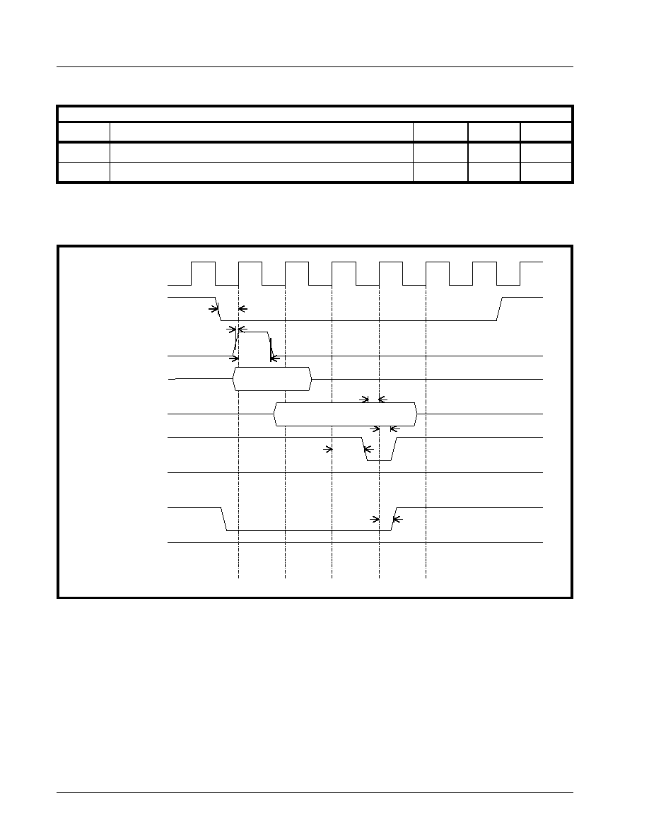
XRT79L71
PRELIMINARY
·Á
·Á
·Á
·Á
REV. P1.0.3
1 - CHANNEL DS3/E3 ATM UNI/PPP COMBO IC
44
MICROPROCESSOR INTERFACE TIMING - IDT3051/52 MODE
N
OTE
: The values for "t0" through "t11" can be found in Table 6.
t11
Clock high to pOE_L low
11
-
-
t12
Clock high to pOE_L high
1.5
-
4.1
F
IGURE
8. S
YNCHRONOUS
M
ODE
4 - IDT 3051/52 I
NTERFACE
TIMING
(W
RITE
C
YCLE
)
T
ABLE
5: T
IMING
I
NFORMATION
FOR
THE
M
ICROPROCESSOR
I
NTERFACE
,
WHEN
CONFIGURED
TO
OPERATE
IN
THE
IBM P
OWER
PC403 M
ODE
Test Conditions: TA = 25∞C, VCC = 3.3V±5% and 2.5V±5%, unless otherwise specified.
T
IMING
D
ESCRIPTION
M
IN
.
T
YP
.
M
AX
.
pCLK
pCS_L
pA[14:0]
pD[7:0]
pRdy_L
pWR_L
pRD_L
t0
t1
t2
t3
t4
t5
t6
Data
pDBEN_L
pALE
Address

·Á
·Á
·Á
·Á
PRELIMINARY
XRT79L71
1 - CHANNEL DS3/E3 ATM UNI/PPP COMBO IC
REV. P1.0.3
45
N
OTE
: The values for "t0" through "t11" can be found in Table 6.
F
IGURE
9. S
YNCHRONOUS
M
ODE
4 - IDT 3051/52 I
NTERFACE
TIMING
(R
EAD
C
YCLE
)
T
ABLE
6: T
IMING
I
NFORMATION
FOR
THE
M
ICROPROCESSOR
I
NTERFACE
,
WHEN
CONFIGURED
TO
OPERATE
IN
THE
IBM P
OWER
PC403 M
ODE
Test Conditions: TA = 25∞C, VCC = 3.3V±5% and 2.5V±5%, unless otherwise specified.
T
IMING
D
ESCRIPTION
M
IN
.
T
YP
.
M
AX
.
t0
pCS_L low to Clock high
6
-
-
t1
pALE high to Clock high
1
-
-
t2
Clock high to pALE low
6
-
-
t3
Data setup time (WRITE cycle)
-
-
N/N
t4
Data hold time (WRITE cycle)
-
-
N/N
t5
Clock high to pRDY_L low
-
-
11
t6
Clock high to pWR_L high
6
-
-
t7
Clock high to Data valid (READ cycle)
-
-
N/N
t8
Clock high to pRDY_L high
-
-
11
t9
pRDY_L high to Data invalid
0
-
-
t7
t8
t9
pCLK
pCS_L
pA[14:0
]
pD[7:0]
pRdy_L
pWR_L
pRD_L
t5
pDBEN_L
pALE
Address
t10
t11
Data
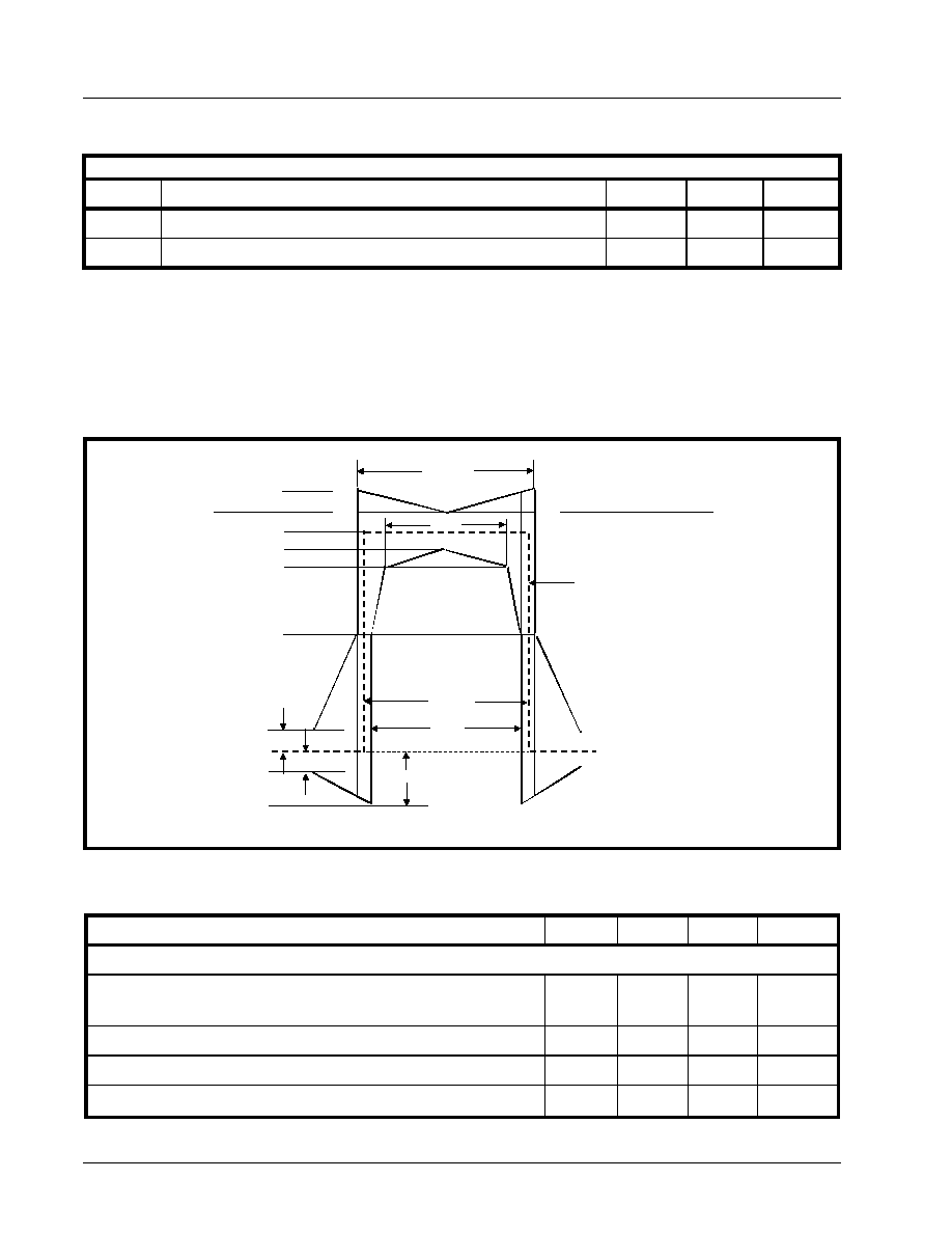
XRT79L71
PRELIMINARY
·Á
·Á
·Á
·Á
REV. P1.0.3
1 - CHANNEL DS3/E3 ATM UNI/PPP COMBO IC
46
DS3/E3 LIU INTERFACE - LINE SIDE ELECTRICAL CHARACTERISTIC INFORMATION
E3 LINE SIDE PARAMETERS
The XRT79L71 line output at the Transmit Output complies with the pulse template requirements as specified
in ITU-T G.703 for 34.368Mbps operation. The pulse mask as specified in ITU-T G.703 for 34.368Mbps is
shown below in Figure 10.
t10
Clock high to pRD_L high
11
-
-
t11
Clock high to pDBEN_L high
10
-
-
F
IGURE
10. P
ULSE
M
ASK
FOR
E3 (34.368M
BPS
) I
NTERFACE
AS
PER
ITU-T G.703
T
ABLE
7: E3 T
RANSMITTER
LINE
SIDE
OUTPUT
AND
RECEIVER
LINE
SIDE
INPUT
SPECIFICATIONS
PARAMETER
MIN
TYP
MAX
UNITS
T
RANSMITTER
LINE
SIDE
OUTPUT
CHARACTERISTICS
Transmit Output Pulse Amplitude
(Measured at secondary of the transformer)
0.9
1.0
1.1
V
pk
Transmit Output Pulse Amplitude Ratio
0.95
1.00
1.05
Transmit Output Pulse Width
12.5
14.55
16.5
ns
Transmit Intrinsic Jitter (without Jitter Attenuator in theTransmit path)
0.01
0.015
UI
PP
T
ABLE
6: T
IMING
I
NFORMATION
FOR
THE
M
ICROPROCESSOR
I
NTERFACE
,
WHEN
CONFIGURED
TO
OPERATE
IN
THE
IBM P
OWER
PC403 M
ODE
Test Conditions: TA = 25∞C, VCC = 3.3V±5% and 2.5V±5%, unless otherwise specified.
T
IMING
D
ESCRIPTION
M
IN
.
T
YP
.
M
AX
.
0%
50%
V = 100%
14.55ns
Nominal Pulse
12.1ns
(14.55 - 2.45)
17 ns
(14.55 + 2.45)
8.65 ns
10%
10%
20%
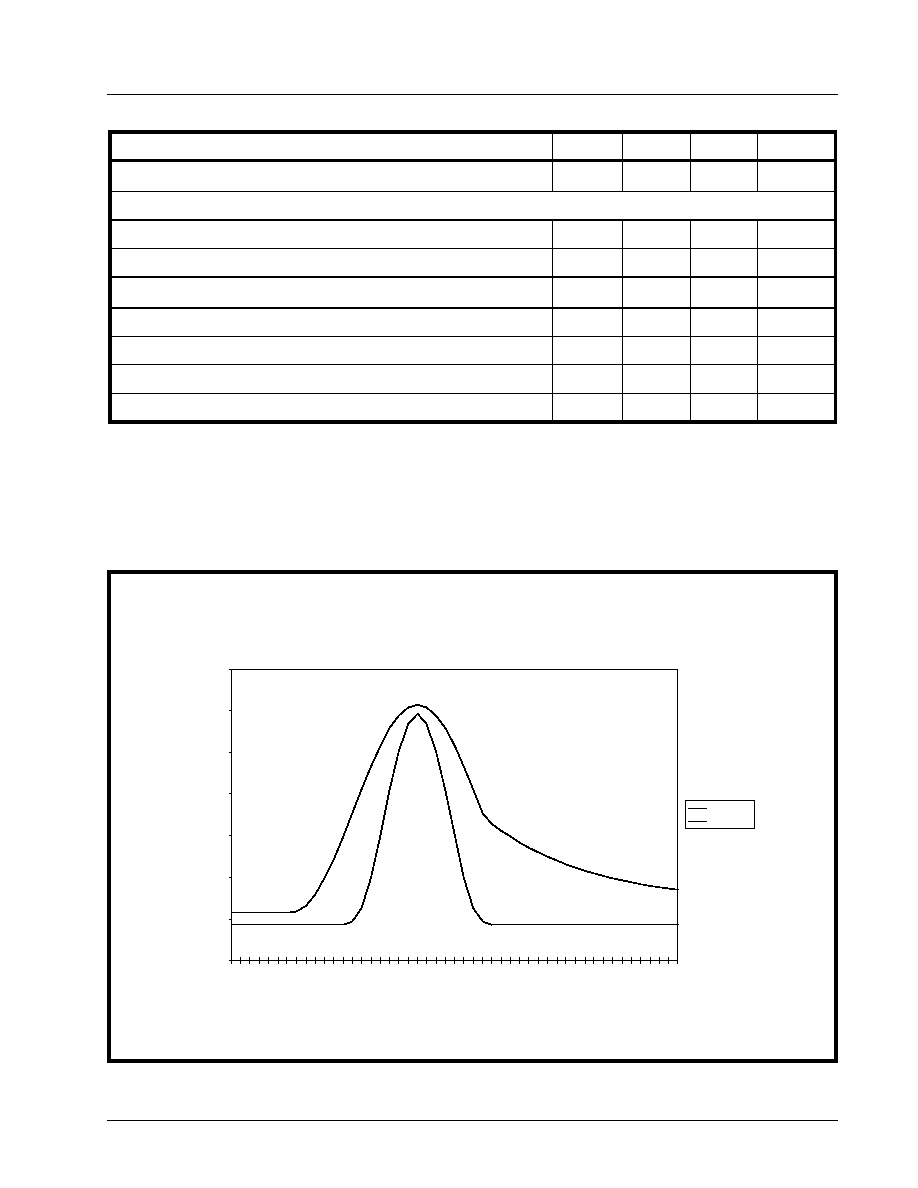
·Á
·Á
·Á
·Á
PRELIMINARY
XRT79L71
1 - CHANNEL DS3/E3 ATM UNI/PPP COMBO IC
REV. P1.0.3
47
DS3 LINE SIDE PARAMETERS
The XRT79L71 will output pulses that comply with the Isolated DSX-3 Pulse Template requirements per
Bellcore GR-499-CORE. The pulse mask as specified in Bellcore GR-499-CORE is shown below in Figure 11.
Additionally, the Equations that define both the "Upper" and "Lower" curves of the Pulse Template requirement
is presented below in Table 8.
Transmit Intrinsic Jitter ( with Jitter Attenuator in the Transmit path)
0.02
0.03
UI
PP
R
ECEIVER
LINE
SIDE
INPUT
CHARACTERISTICS
Receiver Sensitivity (length of cable)
900
1200
feet
Interference Margin
-20
-14
dB
Jitter Tolerance @ Jitter Frequency 800KHz
0.15
0.28
UI
PP
Signal level to Declare Loss of Signal
-35
dB
Signal Level to Clear Loss of Signal
-15
dB
Occurence of LOS to LOS Declaration Time
10
255
UI
Termination of LOS to LOS Clearance Time
10
255
UI
F
IGURE
11. B
ELLCORE
GR-499-CORE P
ULSE
T
EMPLATE
R
EQUIREMENTS
FOR
DS3 A
PPLICATIONS
T
ABLE
7: E3 T
RANSMITTER
LINE
SIDE
OUTPUT
AND
RECEIVER
LINE
SIDE
INPUT
SPECIFICATIONS
PARAMETER
MIN
TYP
MAX
UNITS
D S 3 P u ls e T e m p la te
-0.2
0
0.2
0.4
0.6
0.8
1
1.2
-1
-0
.9
-0
.8
-0
.7
-0
.6
-0
.5
-0
.4
-0
.3
-0
.2
-0
.1
0
0.1
0.2
0.3
0.4
0.5
0.6
0.7
0.8
0.9
1
1.1
1.2
1.3
1.4
T im e , in UI
N
o
r
m
a
l
iz
e
d
A
m
pl
i
t
ude
Lower Curve
Upper Curve
XRT79L71
PRELIMINARY
·Á
·Á
·Á
·Á
REV. P1.0.3
1 - CHANNEL DS3/E3 ATM UNI/PPP COMBO IC
48
T
ABLE
8: DS3 P
ULSE
M
ASK
E
QUATIONS
T
IME
IN
U
NIT
I
NTERVALS
N
ORMALIZED
A
MPLITUDE
LOWER CURVE
-0.85
<
T
<
-0.36
- 0.03
-0.36
<
T
<
0.36
0.36
<
T
<
1.4
- 0.03
UPPER CURVE
-0.85
<
T
<
-0.68
0.03
-0.68
<
T
<
0.36
0.36
<
T
<
1.4
0.08 + 0.407 x e
-1.84[T-0.36]
T
ABLE
9: DS3 T
RANSMITTER
L
INE
S
IDE
O
UTPUT
AND
R
ECEIVER
L
INE
S
IDE
I
NPUT
S
PECIFICATIONS
(GR-499)
P
ARAMETER
M
IN
T
YP
M
AX
U
NITS
T
RANSMITTER
LINE
SIDE
OUTPUT
CHARACTERISTICS
Transmit Output Pulse Amplitude
(measured with TxLEV = 0)
0.65
0.75
0.85
V
pk
Transmit Output Pulse Amplitude
(measured with TxLEV = 1)
0.9
1.0
1.1
V
pk
Transmit Output Pulse Width
10.10
11.18
12.28
ns
Transmit Output Pulse Amplitude Ratio
0.9
1.0
1.1
Transmit Intrinsic Jitter ( without Jitter Attenuator in Transmit path)
0.01
0.015
UI
pp
Transmit Intrinsic Jitter ( withJitter Attenuator in Transmit path)
0.02
0.04
UI
pp
R
ECEIVER
LINE
SIDE
INPUT
CHARACTERISTICS
Receiver Sensitivity (length of cable)
900
1100
feet
Jitter Tolerance @ 400 KHz (Cat II)
0.15
UI
pp
Signal Level to Declare Loss of Signal
Refer to Table 10
Signal Level to Clear Loss of Signal
Refer to Table 10
0.5 1
2
--- 1
T
0.18
-----------
+
sin
+
∑
0.03
≠
0.5 1
2
--- 1
T
0.34
-----------
+
sin
+
∑
0.03
+

·Á
·Á
·Á
·Á
PRELIMINARY
XRT79L71
1 - CHANNEL DS3/E3 ATM UNI/PPP COMBO IC
REV. P1.0.3
49
TRANSMIT UTOPIA INTERFACE
The purpose of the Transmit UTOPIA Interface block is to function as either a Standard UTOPIA Level 1, 2 or 3
Interface as it accepts ATM cell data from either an ATM Layer or ATM Adaptation Layer Processor, and routes
this ATM cell data to the TxFIFO within the XRT79L71.
F
IGURE
12. T
IMING
D
IAGRAM
FOR
THE
T
RANSMIT
UTOPIA I
NTERFACE
B
LOCK
T
ABLE
10: T
IMING
I
NFORMATION
FOR
THE
T
RANSMIT
UTOPIA I
NTERFACE
B
LOCK
S
YMBOL
P
ARAMETER
M
IN
.
T
YP
M
AX
.
U
NITS
t1
TxUData[15:0] to rising edge of TxUClk Setup Time
4
ns
t2
TxUData[15:0] Hold Time from rising edge of TxUClk
1
ns
t3
TxUTOPIA Write Enable Setup Time to rising edge of TxUClk
4
ns
t4
TxUTOPIA Write Enable Hold Time from rising edge of TxUClk
1
ns
t5
TxUPrty Setup Time to rising edge of TxUClk
4
ns
t6
TxUPrty Hold Time from rising edge of TxUClk
1
ns
t7
TxUSoC Setup Time to rising edge of TxUClk
4
ns
t8
TxUSoC Hold Time from rising edge of TxUClk
1
ns
t9
TxUAddr[4:0] Setup Time to rising edge of TxUClk
4
ns
t10
TxUAddr[4:0] Hold Time from rising edge of TxUClk
1
ns
TxUData[15:0]
TxUEn*
TxUPrty
TxUSoC
TxUClk
t1
t3
t2
t5
t7
t6
t8
t4
TxUClav
t11
t12
VALID DATA

XRT79L71
PRELIMINARY
·Á
·Á
·Á
·Á
REV. P1.0.3
1 - CHANNEL DS3/E3 ATM UNI/PPP COMBO IC
50
TRANSMIT PAYLOAD DATA INPUT INTERFACE
TRANSMIT PAYLOAD DATA INPUT INTERFACE - TIMING REQUIREMENTS
t11
TxUClav signal valid (not Hi-Z) from first TxUClk rising edge of
valid and correct TxUAddr[4:0]
3.6
9.7
ns
t12
TxUClav signal Hi-Z from first TxUClk rising edge of different
TxUAddr[4:0]
3.6
9.7
ns
T
ABLE
11: T
IMING
INFORMATION
FO
RTHE
T
RNASMIT
P
AYLOAD
D
ATA
I
NPUT
I
NTERFACE
BLOCK
Test Conditions: TA = 25∞C, VDD = 3.3V + 5% unless otherwise specified
S
YMBOL
P
ARAMETER
M
IN
.
T
YP
.
M
AX
.
U
NITS
C
ONDITIONS
Transmit Payload Data Input Interface - Loop-Timed/Serial Mode (See Figure 13)
t
1
Payload data (TxSer) set-up time to rising edge of
RxOutClk
12
ns
t
2
Payload data (TxSer) hold time, from rising edge of
RxOutClk
0
ns
t
3
RxOutClk to TxFrame output delay
5
ns
t
4
RxOutClk to TxOHInd output delay
6
ns
Transmit Payload Data Input Interface - Local Timed/Serial Mode (See Figure 14)
t
5
Payload data (TxSer) set-up time to rising edge of
TxInClk
4
ns
t
6
Payload data (TxSer) hold time, from rising edge of
TxInClk
0
ns
t
7
TxFrameRef set-up time to rising edge of TxInClk
2
ns
Framer IC is
Frame Slave
t
8
TxFrameRef hold-time, from rising edge of TxInClk
0
ns
Frame IC is
Frame Slave
t
9
TxInClk to TxOHInd output delay
15
ns
t
10
TxInClk to TxFrame output delay
13
ns
Transmit Payload Data Input Interface - Looped-Timed/Nibble Mode (See Figure 15)
t
11
TxNib set-up time to third rising edge of RxOutClk
30
ns
t
12
Payload Nibble hold time, from latching edge of
RxOutClk
30
ns
t
13
TxNibClk to TxNibFrame output delay
25
31
ns
ns
DS3 Applications
E3 Applications
t
13A
Max Delay of Rising Edge of TxNibClk to Data Valid
on TxNib[3:0]
20
27
ns
ns
DS3 Applications
E3 Applications
Transmit Payload Data Input Interface - Local-Timed/Nibble Mode (See Figure 16
T
ABLE
10: T
IMING
I
NFORMATION
FOR
THE
T
RANSMIT
UTOPIA I
NTERFACE
B
LOCK
S
YMBOL
P
ARAMETER
M
IN
.
T
YP
M
AX
.
U
NITS

·Á
·Á
·Á
·Á
PRELIMINARY
XRT79L71
1 - CHANNEL DS3/E3 ATM UNI/PPP COMBO IC
REV. P1.0.3
51
t
14
TxNib set-up time to third rising edge of TxInClk
20
27
ns
ns
DS3 Applications
E3 Applications
t
15
Payload Nibble hold time, from latching edge of
TxInClk
0
ns
t
16
TxFrameRef set-up time, to latching edge of TxInClk
20
27
ns
ns
DS3 Applications
E3 Applications
Framer IC is
Frame Slave
t
17
TxFrameRef hold time, from latching edge of TxNib-
Clk
0
ns
Framer IC is
Frame Slave
t
18
TxNibClk to TxNibFrame output delay time
20
25
31
ns
ns
DS3 Applications
E3 Applications
F
IGURE
13. T
IMING
D
IAGRAM
FOR
THE
T
RANSMIT
P
AYLOAD
D
ATA
I
NPUT
I
NTERFACE
WHEN
THE
XRT79L71
IS
OPER
-
ATING
IN
BOTH
THE
DS3
AND
L
OOP
-T
IMING
M
ODES
T
ABLE
11: T
IMING
INFORMATION
FO
RTHE
T
RNASMIT
P
AYLOAD
D
ATA
I
NPUT
I
NTERFACE
BLOCK
Test Conditions: TA = 25∞C, VDD = 3.3V + 5% unless otherwise specified
S
YMBOL
P
ARAMETER
M
IN
.
T
YP
.
M
AX
.
U
NITS
C
ONDITIONS
XRT79L71 Transmit Payload Data I/F Signals
RxOutClk
TxSer
TxFrame
TxOH_Ind
Payload[4702]
Payload[4703]
X-Bit
Payload[0]
DS3 Frame Number N
DS3 Frame Number N + 1
t1
t2
t3
t4
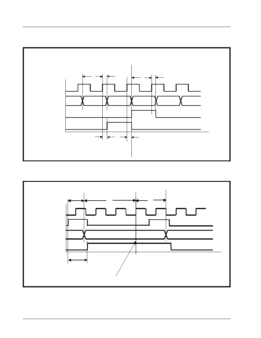
XRT79L71
PRELIMINARY
·Á
·Á
·Á
·Á
REV. P1.0.3
1 - CHANNEL DS3/E3 ATM UNI/PPP COMBO IC
52
F
IGURE
14. T
IMING
D
IAGRAM
FOR
THE
T
RANSMIT
P
AYLOAD
D
ATA
I
NPUT
I
NTERFACE
WHEN
THE
XRT79L71
IS
OPER
-
ATING
IN
BOTH
THE
DS3
AND
L
OCAL
-T
IMING
M
ODES
F
IGURE
15. T
IMING
D
IAGRAM
FOR
THE
T
RANSMIT
P
AYLOAD
D
ATA
I
NPUT
I
NTERFACE
WHEN
THE
XRT79L71
IS
OPER
-
ATING
IN
BOTH
THE
DS3/N
IBBLE
-P
ARALLEL
AND
L
OOP
-T
IMING
M
ODES
XRT79L71 Transmit Payload Data I/F Signals
TxInClk
TxSer
TxFrameRef
TxOH_Ind
Payload[4702]
Payload[4703]
X-Bit
Payload[1]
DS3 Frame Number N
DS3 Frame Number N + 1
t5
t6
t7
t8
t9
t10
RxOutClk
TxNibFrame
TxNibClk
TxNib[3:0]
Nibble [1175]
Nibble [0]
Sampling Edge of XRT79L71
t11
t12
t13
t13A
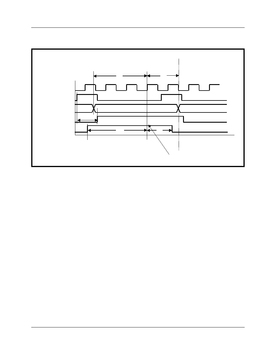
·Á
·Á
·Á
·Á
PRELIMINARY
XRT79L71
1 - CHANNEL DS3/E3 ATM UNI/PPP COMBO IC
REV. P1.0.3
53
F
IGURE
16. T
IMING
D
IAGRAM
FOR
THE
T
RANSMIT
P
AYLOAD
D
ATA
I
NPUT
I
NTERFACE
WHEN
THE
XRT79L71
IS
OPER
-
ATING
IN
BOTH
THE
DS3/N
IBBLE
-P
ARALLEL
AND
L
OCAL
-T
IMING
M
ODES
DS3 Frame Number N
DS3 Frame Number N + 1
TxInClk
TxNibFrame
TxNibClk
TxNib[3:0]
Nibble [1175]
Nibble [0]
Sampling Edge of the XRT79L71
t14
t15
TxFrameRef
t16
t17
t18

XRT79L71
PRELIMINARY
·Á
·Á
·Á
·Á
REV. P1.0.3
1 - CHANNEL DS3/E3 ATM UNI/PPP COMBO IC
54
TRANSMIT OVERHEAD DATA INPUT INTERFACE
TRANSMIT OVERHEAD DATA INPUT INTERFACE - TIMING REQUIREMENTS
T
ABLE
12: T
IMING
I
NFORMATION
FOR
THE
T
RANSMIT
O
VERHEAD
D
ATA
I
NPUT
I
NTERFACE
B
LOCK
Test Conditions: TA = 25∞C, VDD = 3.3V + 5% unless otherwise specified
S
YMBOL
P
ARAMETER
M
IN
.
T
YP
.
M
AX
.
U
NITS
C
ONDITIONS
Transmit Overhead Input Interface Timing - Method 1 (
Figure 17
)
t
21
TxOHClk to TxOHFrame output delay
111
0
0
ns
ns
ns
DS3 Applications
E3, ITU-T G.832
Applications
E3, ITU-T G.751
Applications
t
22
TxOHIns set-up time, to falling edge of TxOHClk
194
305
17
ns
ns
ns
DS3 Applications
E3, ITU-T G.832
Applications
E3, ITU-T G.751
Applications
t
23
TxOHIns hold time, from falling edge of TxOHClk
48
110
7
ns
ns
ns
DS3 Applications
E3, ITU-T G.832
Applications
E3, ITU-T G.751
Applications
t
24
TxOH data set-up time, to falling edge of TxOHClk
194
305
17
ns
ns
ns
DS3 Applications
E3, ITU-T G.832
Applications
E3, ITU-T G.751
Applications
t
25
TxOH data hold time, from falling edge of TxOHClk
48
110
7
ns
ns
ns
DS3 Applications
E3, ITU-T G.832
Applications
E3, ITU-T G.751
Applications
Transmit Overhead Data Input Interface - Method 2 (
Figure 18
)

·Á
·Á
·Á
·Á
PRELIMINARY
XRT79L71
1 - CHANNEL DS3/E3 ATM UNI/PPP COMBO IC
REV. P1.0.3
55
t
26
TXOHIns to TxInClk (rising edge) set-up Time
254
72
15
ns
ns
ns
DS3 Applications
E3, ITU-T G.832
Applications
E3, ITU-T G.751
Applications
t
27
TxInClk clock (rising edge) to TxOHIns hold-time
0
0
0
ns
ns
ns
DS3 Applications
E3, ITU-T G.832
Applications
E3, ITU-T G.751
Applications
t
28
TXOH to TxInClk (rising edge) set-up Time
254
72
15
ns
ns
ns
DS3 Applications
E3, ITU-T G.832
Applications
E3, ITU-T G.751
Applications
t
29
TxInClk clock (rising edge) to TxOH hold-time
0
0
0
ns
ns
ns
DS3 Applications
E3, ITU-T G.832
Applications
E3, ITU-T G.751
Applications
t
29A
TxOHEnable to TxOHIns/TxOH Delay
1
ns
T
ABLE
12: T
IMING
I
NFORMATION
FOR
THE
T
RANSMIT
O
VERHEAD
D
ATA
I
NPUT
I
NTERFACE
B
LOCK
Test Conditions: TA = 25∞C, VDD = 3.3V + 5% unless otherwise specified
S
YMBOL
P
ARAMETER
M
IN
.
T
YP
.
M
AX
.
U
NITS
C
ONDITIONS
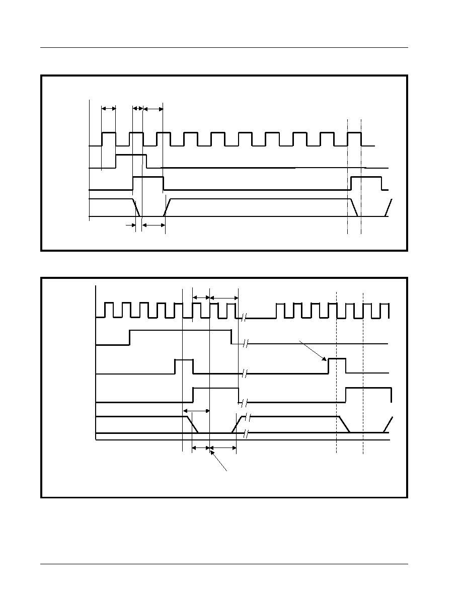
XRT79L71
PRELIMINARY
·Á
·Á
·Á
·Á
REV. P1.0.3
1 - CHANNEL DS3/E3 ATM UNI/PPP COMBO IC
56
F
IGURE
17. T
IMING
D
IAGRAM
FOR
THE
T
RANSMIT
O
VERHEAD
D
ATA
I
NPUT
I
NTERFACE
(M
ETHOD
1 A
CCESS
)
F
IGURE
18. T
IMING
D
IAGRAM
FOR
THE
T
RANSMIT
O
VERHEAD
D
ATA
I
NPUT
I
NTERFACE
(M
ETHOD
2 A
CCESS
)
TxOHClk
TxOHIns
TxOHFrame
TxOH
Remaining Overhead Bits with DS3 Frame
X bit = 0
X bit = 0
t21
t22
t24
t23
t25
TxInClk
TxOHFrame
TxOHEnable
TxOHIns
TxOH
XRT79L71 samples TxOH here.
TxOHEnable Pulse # 8
X bit = 0
X bit = 0
t26
t27
t28
t29
t29A

·Á
·Á
·Á
·Á
PRELIMINARY
XRT79L71
1 - CHANNEL DS3/E3 ATM UNI/PPP COMBO IC
REV. P1.0.3
57
RECEIVE PAYLOAD DATA OUTPUT INTERFACE
RECEIVE PAYLOAD DATA OUTPUT INTERFACE - TIMING REQUIREMENTS
T
ABLE
13: T
IMING
I
NFORMATION
FOR
THE
R
ECEIVE
P
AYLOAD
D
ATA
O
UTPUT
I
NTERFACE
B
LOCK
Test Conditions: TA = 25∞C, VDD = 3.3V + 5% unless otherwise specified
S
YMBOL
P
ARAMETER
M
IN
.
T
YP
.
M
AX
.
U
NITS
C
ONDITIONS
Receive Payload Data Output Interface Timing - Serial Mode Operation (See Figure 19)
t
50
Rising edge of RxClk to Payload Data (RxSer) out-
put delay
13
16
ns
ns
DS3 Applications
E3 Applications
t
51
Rising edge of RxClk to RxFrame output delay
13
16
ns
ns
DS3 Applications
E3 Applications
t
52
Rising edge of RxClk to RxOHInd output delay.
13
16
ns
ns
DS3 Applications
E3 Applications
Receive Payload Data Output Interface Timing - Nibble Mode Operation (see Figure 20)
t
53
Falling edge of RxClk to rising edge of RxFrame out-
put delay
2.1
ns
t
54
Falling edge of RxClk to rising edge of RxNib[3:0]
output delay
2
ns
F
IGURE
19. T
IMING
D
IAGRAM
FOR
THE
R
ECEIVE
P
AYLOAD
D
ATA
O
UTPUT
I
NTERFACE
(S
ERIAL
M
ODE
)
XRT79L71 Receive Payload Data I/F Signals
RxClk
RxSer
RxFrame
RxOHInd
Payload[4702]
Payload[4703]
X-Bit
Payload[0]
t50
t51
t52

XRT79L71
PRELIMINARY
·Á
·Á
·Á
·Á
REV. P1.0.3
1 - CHANNEL DS3/E3 ATM UNI/PPP COMBO IC
58
F
IGURE
20. T
IMING
D
IAGRAM
FOR
THE
R
ECEIVE
P
AYLOAD
D
ATA
O
UTPUT
I
NTERFACE
(N
IBBLE
-P
ARALLEL
M
ODE
)
DS3 Frame Number N
DS3 Frame Number N + 1
RxOutClk
RxFrame
RxClk
RxNib[3:0]
Nibble [0]
Nibble [1]
Recommended Sampling Edge of Terminal
Equipment
t53
t54
XRT79L71 Receive Payload Data I/F Signals

·Á
·Á
·Á
·Á
PRELIMINARY
XRT79L71
1 - CHANNEL DS3/E3 ATM UNI/PPP COMBO IC
REV. P1.0.3
59
RECEIVE OVERHEAD DATA OUTPUT INTERFACE
RECEIVE OVERHEAD DATA OUTPUT INTERFACE - TIMING REQUIREMENTS
Table 13, Timing Information for the Receive Overhead Data Output Interface Block
AC ELECTRICAL CHARACTERISTICS (CONT.)
Test Conditions: TA = 25∞C, VDD = 3.3V + 5% unless otherwise specified
S
YMBOL
P
ARAMETER
M
IN
.
T
YP
.
M
AX
.
U
NITS
C
ONDITIONS
Receive Overhead Data Output Interface Timing - Method 1 - Using RxOHClk (see Figure 17)
t
59A
Falling edge of RxOHClk to RxOHFrame output
20
25
23
0
ns
ns
DS3 Applications
E3 Applications
t
59B
Falling edge of RxOHClk to RxOH output delay
20
25
23
0
ns
ns
DS3 Applications
E3 Applications
Receive Overhead Data Output Interface Timing - Method 2 - Using RxOHEnable (see Figure 18)
t
60
Rising edge of RxOutClk to rising edge of
RxOHEnable delay.
2
9.4
ns
t
60A
Rising edge of RxOHFrame to rising edge of
RxOHEnable delay
88
224
28
ns
ns
ns
DS3 Applications
E3, ITU-T G.832
Applications
E3, ITU-T G.751
Applications
t
60B
RxOH Data Valid to rising edge of
RxOHEnable delay
88
85
28
ns
ns
ns
DS3 Applications
E3, ITU-T G.832
Applications
E3, ITU-T G.751
Applications

XRT79L71
PRELIMINARY
·Á
·Á
·Á
·Á
REV. P1.0.3
1 - CHANNEL DS3/E3 ATM UNI/PPP COMBO IC
60
F
IGURE
21. T
IMING
D
IAGRAM
FOR
THE
R
ECEIVE
O
VERHEAD
D
ATA
O
UTPUT
I
NTERFACE
(M
ETHOD
1 - U
SING
R
X
O-
HC
LK
)
F
IGURE
22. T
IMING
D
IAGRAM
FOR
THE
R
ECEIVE
O
VERHEAD
D
ATA
O
UTPUT
I
NTERFACE
(M
ETHOD
2 - U
SING
R
X
O-
HE
NABLE
)
RxOHClk
RxOHFrame
RxOH
X F1 AIC
F0 FEAC
t59A
t59B
RxOutClk
RxOHEnable
RxOHFrame
RxOH
UDL F1
X1 F1
AIC
t60
t60A
t60B

·Á
·Á
·Á
·Á
PRELIMINARY
XRT79L71
1 - CHANNEL DS3/E3 ATM UNI/PPP COMBO IC
REV. P1.0.3
61
RECEIVE UTOPIA INTERFACE
RECEIVE UTOPIA INTERFACE
The purpose of the Receive UTOPIA Interface block is to function as either a Standard UTOPIA Level 1, 2 or 3
Interface as it outputs ATM cell data to either an ATM Layer or ATM Adaptation Layer Processor.
F
IGURE
23. T
IMING
D
IAGRAM
FOR
THE
R
ECEIVE
UTOPIA I
NTERFACE
B
LOCK
T
ABLE
14: T
IMING
I
NFORMATION
FOR
THE
R
ECEIVE
UTOPIA I
NTERFACE
B
LOCK
Symbol
P
ARAMETER
M
IN
.
T
YP
M
AX
.
U
NITS
Receive UTOPIA Interface Block (See Figure 22)
t53
Delay time from rising edge of RxUClk to Data Valid at RxU-
Data[15:0]
2.7
12
ns
t54
Rx UTOPIA Read Enable setup time to rising edge of RxUClk
4
ns
t55
Delay time from rising edge of RxUClk to valid RxUPrty bit
2.9
9.8
ns
t56
Delay time from rising edge of RxUClk to valid RxUSoC bit
3.5
9.7
ns
t57
Delay time from Read Enable false to Data Bus being tri-stated
1
11.5
16
ns
t58
Delay time from Read Enable false to RxUPrty bit being tri-
stated
1
12
16
ns
RxUData[15:0]
RxUEn*
RxUPrty
RxUSoC
RxUClk
t54
t57
RxUClav
t62
t63
t53
DATA VALID
t55
t58
t59
t56

XRT79L71
PRELIMINARY
·Á
·Á
·Á
·Á
REV. P1.0.3
1 - CHANNEL DS3/E3 ATM UNI/PPP COMBO IC
62
t59
Delay time from Read Enable false to RxUSoC bit being tri-
stated
1
11.5
16
ns
t61
RxUAddr[4:0] Hold Time from rising edge of RxUClk
1
ns
t62
RxUClav signal valid (not Hi-Z) from first RxUClk rising edge of
valid and correct RxUAddr[4:0]
2.5
8.6
ns
t63
RxUClav signal Hi-Z from first RxUClk rising edge of different
RxUAddr[4:0].
2.5
8.6
ns
t58
Delay time from Read Enable false to RxUPrty bit being tri-
stated
1
12
16
ns
t59
Delay time from Read Enable false to RxUSoC bit being tri-
stated
1
11.5
16
ns
t60
RxUAddr[4:0] Setup Time to rising edge of RxUClk
4
ns
t61
RxUAddr[4:0] Hold Time from rising edge of RxUClk
1
ns
t62
RxUClav signal valid (not Hi-Z) from first RxUClk rising edge of
valid and correct RxUAddr[4:0]
1
7.8
16
ns
t63
RxUClav signal Hi-Z from first RxUClk rising edge of different
RxUAddr[4:0].
1
9.2
16
ns
T
ABLE
14: T
IMING
I
NFORMATION
FOR
THE
R
ECEIVE
UTOPIA I
NTERFACE
B
LOCK
Symbol
P
ARAMETER
M
IN
.
T
YP
M
AX
.
U
NITS

·Á
·Á
·Á
·Á
PRELIMINARY
XRT79L71
1 - CHANNEL DS3/E3 ATM UNI/PPP COMBO IC
REV. P1.0.3
63
REGISTER MAP OF THE XRT79L71
COMMONCONTROL REGISTERS OF THE XRT79L71
A
DDRESS
L
OCATION
R
EGISTER
N
AME
T
YPE
D
EFAUL
V
ALUE
COMMON CONTROL REGISTERS
0x0100
Operation Control Register - Byte 3
R/W
0x00
0x0101
Operation Control Register - Byte 2
R/W
0x00
0x0102
Operation Control Register - Byte 1
R/W
0x00
0x0103
Operation Control Register - Byte 0
R/W
0x00
0x0104
Device ID Register
R/W
?x??
0x0105
Revision ID Register
R/W
?x??
0x0106 - 0x0111
Reserved
0x0112
Operation Block Interrupt Status Register - Byte 1
RO
0x00
0x0113
Operation Block Interrupt Status Register - Byte 0
RO
0x00
0x0114 - 0x0115
Reserved
0x0116
Operation Block Interrupt Enable Register - Byte 1
R/W
0x00
0x0117
Operation Block Interrupt Enable Register - Byte 0
R/W
0x00
0x0118
Reserved
0x0119
Channel Interrupt Indicator - Receive Cell Processor/PPP Processor
Block
R/O
0x00
0x011A - 0x011C
Reserved
0x011D
Channel Interrupt Indicator - LIU/Jitter Attenuator Block
R/O
0x00
0x011E - 0x0120
Reserved
0x0121
Channel Interrupt Indicator - Transmit Cell Processor/PPP Processor
Block
R/O
0x00
0x0122 - 0x0126
Reserved
0x0127
Channel Interrupt Indicator - DS3/E3 Framer Block - Byte 0
R/O
0x00
0x0128 - 0x0146
Reserved
0x0147
Operation General Purpose Input/Output Register
R/W
0x00
0x0148 - 0x014A
Reserved
0x014B
Operation General Purpose Input/Output Direction Register
R/W
0x00
0x014C - 0x04FF
Reserved
0x0501
Receive POS-PHY Control Register - Byte 1
R/W
0x00
0x0502
Receive POS-PHY Control Register - Byte 0
R/W
0x00
0x0503
Receive UTOPIA Control Register
R/W
0x00
0x0504 - 0x0512
Reserved

XRT79L71
PRELIMINARY
·Á
·Á
·Á
·Á
REV. P1.0.3
1 - CHANNEL DS3/E3 ATM UNI/PPP COMBO IC
64
0x0513
Receive UTOPIA Port Address Register
0x0514 - 0x0516
Reserved
0x0517
Receive UTOPIA Port Number Register
R/W
0x00
0x0518 - 0x0580
Reserved
0x0581
Transmit POS-PHY Control Register - Byte 1
R/W
0x00
0x0582
Transmit POS-PHY Control Register - Byte 0
R/W
0x00
0x0583
Transmit UTOPIA Control Register
R/W
0x00
0x0584 - 0x0592
Reserved
0x0593
Transmit UTOPIA Port Address Register
R/W
0x00
0x0594 - 0x0596
Reserved
0x0597
Transmit UTOPIA Port Number Register
R/W
0x00
CLEAR-CHANNEL FRAMER BLOCK REGISTERS
A
DDRESS
L
OCATION
R
EGISTER
N
AME
T
YPE
D
EFAULT
V
ALUE
CHANNEL CONTROL REGISTERS
CLEAR-CHANNEL FRAMER BLOCK REGISTERS
0x1100
Operating Mode Register
R/W
0x2B
0x1101
I/O Control Register
R/W
0xC0
0x1102 - 0x1103
Reserved
0x1104
Block Interrupt Enable Register
R/W
0x00
0x1105
Block Interrupt Status Register
R/O
0x00
0x1106 - 0x110B
Reserved
0x110C
DS3 Test Register
R/W
0x00
0x110D
Payload HDLC Control Register
R/W
0x00
0x110E - 0x110F
Reserved
0x1110
RxDS3 Configuration and Status RegisterRxE3 Configuration and Status
Register # 1 (G.832 & G.751)
R/O
0x12
0x1111
RxDS3 Status RegisterRxE3 Configuration and Status Register # 2
(G.832 & G.751)
R/O
0x00
0x1112
RxDS3 Interrupt Enable RegisterRxE3 Interrupt Enable Register 1
(G.832 & G751)
R/W
0x00
0x1113
RxDS3 Interrupt Status RegisterRxE3 Interrupt Enable Register # 2
(G.832 & G.751)
RUR
0x00
COMMONCONTROL REGISTERS OF THE XRT79L71
A
DDRESS
L
OCATION
R
EGISTER
N
AME
T
YPE
D
EFAUL
V
ALUE
COMMON CONTROL REGISTERS

·Á
·Á
·Á
·Á
PRELIMINARY
XRT79L71
1 - CHANNEL DS3/E3 ATM UNI/PPP COMBO IC
REV. P1.0.3
65
0x1114
RxDS3 Sync Detect RegisterRxE3 Interrupt Status Register # 1 (G.832 &
G.751)
R/W &
RUR
0x00
0x1115
RxE3 Interrupt Status Register # 2 (G.832 & G.751)
RUR
0x00
0x1116
Reserved
0x1117
RxDS3 FEAC Interrupt Enable and Status Register
R/W &
RUR
0x00
0x1118
RxE3 LAPD Control Register
R/W &
RUR
0x00
0x1119
RxLAPD Status Register
R/O
0x00
0x111A
RxE3 NR Byte Register (G.832)RxE3 Service Bits Register (G.751)
R/O
0x00
0x111B
RxE3 GC Byte Register (G.832)
R/O
0x00
0x111C
RxE3 TTB Register # 0 (G.832)
R/O
0x00
0x111D
RxE3 TTB Register # 1 (G.832)
R/O
0x00
0x111E
RxE3 TTB Register # 2 (G.832)
R/O
0x00
0x111F
RxE3 TTB Register # 3 (G.832)
R/O
0x00
0x1120
RxE3 TTB Register # 4 (G.832)
R/O
0x00
0x1121
RxE3 TTB Register # 5 (G.832)
R/O
0x00
0x1122
RxE3 TTB Register # 6 (G.832)
R/O
0x00
0x1123
RxE3 TTB Register # 7 (G.832)
R/O
0x00
0x1124
RxE3 TTB Register # 8 (G.832)
R/O
0x00
0x1125
RxE3 TTB Register # 9 (G.832)
R/O
0x00
0x1126
RxE3 TTB Register # 10 (G.832)
R/O
0x00
0x1127
RxE3 TTB Register # 11 (G.832)
R/O
0x00
0x1128
RxE3 TTB Register # 12 (G.832)
R/O
0x00
0x1129
RxE3 TTB Register # 13 (G.832)
R/O
0x00
0x112A
RxE3 TTB Register # 14 (G.832)
R/O
0x00
0x112B
RxE3 TTB Register # 15 (G.832)
R/O
0x00
0x112C
RxE3 SSM Register (G.832)
R/O
0x00
0x112D - 0x112F
Reserved
0x1130
Transmit DS3 Configuration RegisterTransmit E3 Configuration Register
R/W
0x07
0x1131
TxDS3 FEAC Configuration and Status Register
RUR &
R/W
0x00
CLEAR-CHANNEL FRAMER BLOCK REGISTERS
A
DDRESS
L
OCATION
R
EGISTER
N
AME
T
YPE
D
EFAULT
V
ALUE
CHANNEL CONTROL REGISTERS
CLEAR-CHANNEL FRAMER BLOCK REGISTERS

XRT79L71
PRELIMINARY
·Á
·Á
·Á
·Á
REV. P1.0.3
1 - CHANNEL DS3/E3 ATM UNI/PPP COMBO IC
66
0x1132
TxDS3 FEAC Register
R/W
0x7E
0x1133
TxLAPD Configuration Register
R/O & R/
W
0x08
0x1134
TxLAPD Status and Interrupt Register
RUR &
R/W
0x00
0x1135
TxDS3 M-Bit Mask RegisterTxE3 GC Byte Register (G.832)TxE3 Service
Bits Register (G.751)
R/W
0x00
0x1136
TxDS3 F-Bit Mask Register # 1TxE3 MA Byte Register (G.832)
R/W
0x00
0x1137
TxDS3 F-Bit Mask Register # 2TxE3 NR Byte Register (G.832)
R/W
0x00
0x1138
TxDS3 F-Bit Mask Register # 3TxTTB Register # 0 (G.832)
R/W
0x00
0x1139
TxTTB Register # 1 (G.832)
R/W
0x00
0x113A
TxTTB Register # 2 (G.832)
R/W
0x00
0x113B
TxTTB Register # 3 (G.832)
R/W
0x00
0x113C
TxTTB Register # 4 (G.832)
R/W
0x00
0x113D
TxTTB Register # 5 (G.832)
R/W
0x00
0x113E
TxTTB Register # 6 (G.832)
R/W
0x00
0x113F
TxTTB Register # 7 (G.832)
R/W
0x00
0x1140
TxTTB Register # 8 (G.832)
R/W
0x00
0x1141
TxTTB Register # 9 (G.832)
R/W
0x00
0x1142
TxTTB Register # 10 (G.832)
R/W
0x00
0x1143
TxTTB Register # 11 (G.832)
R/W
0x00
0x1144
TxTTB Register # 12 (G.832)
R/W
0x00
0x1145
TxTTB Register # 13 (G.832)
R/W
0x00
0x1146
TxTTB Register # 14 (G.832)
R/W
0x00
0x1147
TxTTB Register # 15 (G.832)
R/W
0x00
0x1148
TxE3 FA1 Error Mask Register (G.832)TxE3 FAS Error Mask Register # 1
(G.751)
R/W
0x00
0x1149
TxE3 FA2 Error Mask Register (G.832)TxE3 FAS Error Mask Register # 2
(G.751)
R/W
0x00
0x114A
TxE3 BIP-8 Error Mask Register (G.832)TxE3 BIP-4 Error Mask Register
(G.751)
R/W
0x00
0x114B
TxE3 SSM Register
R/W
0x00
0x114C - 0x114F
Reserved
R/O
0x00
CLEAR-CHANNEL FRAMER BLOCK REGISTERS
A
DDRESS
L
OCATION
R
EGISTER
N
AME
T
YPE
D
EFAULT
V
ALUE
CHANNEL CONTROL REGISTERS
CLEAR-CHANNEL FRAMER BLOCK REGISTERS

·Á
·Á
·Á
·Á
PRELIMINARY
XRT79L71
1 - CHANNEL DS3/E3 ATM UNI/PPP COMBO IC
REV. P1.0.3
67
0x1150
PMON Line Code Violation Count Register - MSB
RUR
0x00
0x1151
PMON Line Code Violation Count Register - LSB
RUR
0x00
0x1152
PMON Framing Bit/Byte Error Count Register - MSB
RUR
0x00
0x1153
PMON Framing Bit/Byte Error Count Register - LSB
RUR
0x00
0x1154
PMON P-Bit/BIP-8/BIP-4 Error Count Register - MSB
RUR
0x00
0x1155
PMON P-Bit/BIP-8/BIP-4 Error Count Register - LSB
RUR
0x00
0x1156
PMON FEBE Event Count Register - MSB
RUR
0x00
0x1157
PMON FEBE Event Count Register - LSB
RUR
0x00
0x1158
PMON CP-Bit Error Count Register - MSB
RUR
0x00
0x1159
PMON CP-Bit Error Count Register - LSB
RUR
0x00
0x115A
PMON PLCP BIP-8 Error Count Register - MSB
RUR
0x00
0x115B
PMON PLCP BIP-8 Error Count Register - LSB
RUR
0x00
0x115C
PMON PLCP Framing Byte Error Count Register - MSB
RUR
0x00
0x115D
PMON PLCP Framing Byte Error Count Register - LSB
RUR
0x00
0x115E
PMON PLCP FEBE Event Count Register - MSB
RUR
0x00
0x115F
PMON PLCP FEBE Event Count Register - LSB
RUR
0x00
0x1160 - 0x1167
Reserved
0x1168
PRBS Error Count Register - MSB
RUR
0x00
0x1169
PRBS Error Count Register - LSB
RUR
0x00
0x116A - 0x116C
Reserved
0x116D
One Second Error Status Register
R/O
0x00
0x116E
One Second Accumulator - LCV Count Register - MSB
R/O
0x00
0x116F
One Second Accumulator - LCV Count Register - LSB
R/O
0x00
0x1170
One Second Accumulator - P-Bit/BIP-8/BIP-4 Error Count Register -
MSB
R/O
0x00
0x1171
One Second Accumulator - P-Bit/BIP-8/BIP-4 Error Count Register - LSB
R/O
0x00
0x1172
One Second Accumulator - CP Bit Error Count Register - MSB
R/O
0x00
0x1173
One Second Accumulator - CP Bit Error Count Register - LSB
R/O
0x00
0x1174 - 0x117F
Reserved
0x1180
Line Interface Drive Register
R/W
0x08
0x1181
Line Interface Scan Register
R/O
0x00
CLEAR-CHANNEL FRAMER BLOCK REGISTERS
A
DDRESS
L
OCATION
R
EGISTER
N
AME
T
YPE
D
EFAULT
V
ALUE
CHANNEL CONTROL REGISTERS
CLEAR-CHANNEL FRAMER BLOCK REGISTERS

XRT79L71
PRELIMINARY
·Á
·Á
·Á
·Á
REV. P1.0.3
1 - CHANNEL DS3/E3 ATM UNI/PPP COMBO IC
68
0x1182 - 0x118F
Reserved
0x1190
RxPLCP Configuration & Status Register
R/O & R/
W
0x06
0x1191
RxPLCP Interrupt Enable Register
R/W
0x00
0x1192
RxPLCP Interrupt Status Register
RUR
0x00
0x1193 - 0x1197
Reserved
0x1198
TxPLCP A1 Byte Error Mask Register
R/W
0x00
0x1199
TxPLCP A2 Byte Error Mask Register
R/W
0x00
0x119A
TxPLCP BIP-8 Byte Error Mask Register
R/W
0x00
0x119B
TxPLCP G1 Byte Register
R/W
0x00
0x119C - 0x12FF
Reserved
LIU/JITTER ATTENUATOR CONTROL REGISTERS
A
DDRESS
L
OCATION
R
EGISTER
N
AME
T
YPE
D
EFAULT
V
ALUE
CHANNEL CONTROL REGISTERS
LIU/JITTER ATTENUATOR CONTROL REGISTERS
0x1300
LIU Transmit APS/Redundancy Control Register
R/W
0x00
0x1301
LIU Interrupt Enable Register
R/W
0x00
0x1302
LIU Interrupt Status Register
RUR
0x00
0x1303
LIU Alarm Status Register
R/O
0x00
0x1304
LIU Transmit Control Register
R/W
0x00
0x1305
LIU Receive Control Register
R/W
0x00
0x1306
LIU Channel Control Register
R/W
0x00
0x1307
Jitter Attenuator Control Register
R/W
0x00
0x1308
LIU Receive APS/Redundancy Control Register
R/W
0x00
CLEAR-CHANNEL FRAMER BLOCK REGISTERS
A
DDRESS
L
OCATION
R
EGISTER
N
AME
T
YPE
D
EFAULT
V
ALUE
CHANNEL CONTROL REGISTERS
CLEAR-CHANNEL FRAMER BLOCK REGISTERS

·Á
·Á
·Á
·Á
PRELIMINARY
XRT79L71
1 - CHANNEL DS3/E3 ATM UNI/PPP COMBO IC
REV. P1.0.3
69
RECEIVE ATM CELL PROCESSOR/PPP PROCESSOR BLOCK CONTROL REGISTERS
A
DDRESS
L
OCATION
R
EGISTER
N
AME
T
YPE
D
EFAULT
V
ALUE
CHANNEL CONTROL REGISTERS
RECEIVE ATM CELL PROCESSOR/PPP PROCESSOR BLOCK CONTROL REGISTERS
0x1700
Receive ATM Control - Byte 3
R/W
0x00
0x1701
Receive ATM Control - Byte 2
R/W
0x00
0x1702
Receive ATM Control - Byte 1
R/W
0x00
0x1703
Receive ATM Control - Byte 0Receive PPP Control Register
R/W
0x00
0x1704 - 0x1706
Reserved
0x1707
Receive ATM Status Register
R/O
0x00
0x1708 - 0x1709
Reserved
0x170A
Receive ATM Interrupt Status Register -Byte 1
RUR
0x00
0x170B
Receive ATM Interrupt Status Register - Byte 0Receive PPP Interrupt
Status Register
RUR
0x00
0x170C - 0x170D
Reserved
0x170E
Receive ATM Interrupt Enable Register - Byte 1
R/W
0x00
0x170F
Receive ATM Interrupt Enable Register - Byte 0Receive PPP Interrupt
Enable Register
R/W
0x00
0x1710
Receive PPP Good Packet Count Register - Byte 3
RUR
0x00
0x1711
Receive PPP Good Packet Count Register - Byte 2
RUR
0x00
0x1712
Receive PPP Good Packet Count Register - Byte 1
RUR
0x00
0x1713
Receive ATM Cell Insertion/Extraction Memory Control RegisterReceive
PPP Good Packet Count Register - Byte 0
R/O & R/
W
0x00
0x1714
Receive ATM Cell Insertion/Extraction Memory Data Register - Byte
3Receive PPP FCS Error Count Register - Byte 3
R/O & R/
W
0x00
0x1715
Receive ATM Cell Insertion/Extraction Memory Data Register - Byte
2Receive PPP FCS Error Count Register - Byte 2
R/O & R/
W
0x00
0x1716
Receive ATM Cell Insertion/Extraction Memory Data Register - Byte
1Receive PPP FCS Error Count Register - Byte 1
R/O & R/
W
0x00
0x1717
Receive ATM Cell Insertion/Extraction Memory Data Register - Byte
0Receive PPP FCS Error Count Register - Byte 0
R/O & R/
W
0x00
0x1718
Receive ATM Cell UDF Data Register - Byte 3Receive PPP Abort Count
Register - Byte 3
R/W &
RUR
0x00
0x1719
Receive ATM Cell UDF Data Register - Byte 2Receive PPP Abort Count
Register - Byte 2
R/W &
RUR
0x00
0x171A
Receive ATM Cell UDF Data Register - Byte 1Receive PPP Abort Count
Register - Byte 1
R/W &
RUR
0x00

XRT79L71
PRELIMINARY
·Á
·Á
·Á
·Á
REV. P1.0.3
1 - CHANNEL DS3/E3 ATM UNI/PPP COMBO IC
70
0x171B
Receive ATM Cell UDF Data Register - Byte 0Receive PPP Abort Count
Register - Byte 0
R/W &
RUR
0x00
0x171C
Receive PPP Runt Frame Count Register - Byte 3
RUR
0x00
0x171D
Receive PPP Runt Frame Count Register - Byte 2
RUR
0x00
0x171E
Receive PPP Runt Frame Count Register - Byte 1
RUR
0x00
0x171F
Receive PPP Runt Frame Count Register - Byte 0
RUR
0x00
0x1720
Receive ATM - Test Cell Header Byte Register - Byte 0
R/W
0x00
0x1721
Receive ATM - Test Cell Header Byte Register - Byte 1
R/W
0x00
0x1722
Receive ATM - Test Cell Header Byte Register - Byte 2
R/W
0x00
0x1723
Receive ATM - Test Cell Header Byte Register - Byte 3
R/W
0x00
0x1724
Receive ATM - Test Cell Error Count Register - Byte 3
RUR
0x00
0x1725
Receive ATM - Test Cell Error Count Register - Byte 2
RUR
0x00
0x1726
Receive ATM - Test Cell Error Count Register - Byte 1
RUR
0x00
0x1727
Receive ATM - Test Cell Error Count Register - Byte 0
RUR
0x00
0x1728
Receive ATM Cell Count Register - Byte 3
RUR
0x00
0x1729
Receive ATM Cell Count Register - Byte 2
RUR
0x00
0x172A
Receive ATM Cell Count Register - Byte 1
RUR
0x00
0x172B
Receive ATM Cell Count Register - Byte 0
RUR
0x00
0x172C
Receive ATM Cell - Discard Cell Count Register - Byte 3
RUR
0x00
0x172D
Receive ATM Cell - Discard Cell Count Register - Byte 2
RUR
0x00
0x172E
Receive ATM Cell - Discard Cell Count Register - Byte 1
RUR
0x00
0x172F
Receive ATM Cell - Discard Cell Count Register - Byte 0
RUR
0x00
0x1730
Receive ATM Correctable HEC Byte Error Count Register - Byte 3
RUR
0x00
0x1731
Receive ATM Correctable HEC Byte Error Count Register - Byte 2
RUR
0x00
0x1732
Receive ATM Correctable HEC Byte Error Count Register - Byte 1
RUR
0x00
0x1733
Receive ATM Correctable HEC Byte Error Count Register - Byte 0
RUR
0x00
0x1734
Receive ATM Uncorrectable HEC Byte Error Count Register - Byte 3
RUR
0x00
0x1735
Receive ATM Uncorrectable HEC Byte Error Count Register - Byte 2
RUR
0x00
0x1736
Receive ATM Uncorrectable HEC Byte Error Count Register - Byte 1
RUR
0x00
0x1737
Receive ATM Uncorrectable HEC Byte Error Count Register - Byte 0
RUR
0x00
0x1738 - 0x1742
Reserved
RECEIVE ATM CELL PROCESSOR/PPP PROCESSOR BLOCK CONTROL REGISTERS
A
DDRESS
L
OCATION
R
EGISTER
N
AME
T
YPE
D
EFAULT
V
ALUE
CHANNEL CONTROL REGISTERS
RECEIVE ATM CELL PROCESSOR/PPP PROCESSOR BLOCK CONTROL REGISTERS

·Á
·Á
·Á
·Á
PRELIMINARY
XRT79L71
1 - CHANNEL DS3/E3 ATM UNI/PPP COMBO IC
REV. P1.0.3
71
0x1743
Receive ATM - User Cell Filter # 0 - Filter Control Register
R/W
0x00
0x1744
Receive ATM - User Cell Filter # 0 - Header Byte # 1 Pattern Register
R/W
0x00
0x1745
Receive ATM - User Cell Filter # 0 - Header Byte # 2 Pattern Register
R/W
0x00
0x1746
Receive ATM - User Cell Filter # 0 - Header Byte # 3 Pattern Register
R/W
0x00
0x1747
Receive ATM - User Cell Filter # 0 - Header Byte # 4 Pattern Register
R/W
0x00
0x1748
Receive ATM - User Cell Filter # 0 - Header Byte # 1 Check Register
R/W
0x00
0x1749
Receive ATM - User Cell Filter # 0 - Header Byte # 2 Check Register
R/W
0x00
0x174A
Receive ATM - User Cell Filter # 0 - Header Byte # 3 Check Register
R/W
0x00
0x174B
Receive ATM - User Cell Filter # 0 - Header Byte # 4 Check Register
R/W
0x00
0x174C
Receive ATM - User Cell Filter # 0 - Filtered Cell Count Register - Byte 3
RUR
0x00
0x174D
Receive ATM - User Cell Filter # 0 - Filtered Cell Count Register - Byte 2
RUR
0x00
0x174E
Receive ATM - User Cell Filter # 0 - Filtered Cell Count Register - Byte 1
RUR
0x00
0x174F
Receive ATM - User Cell Filter # 0 - Filtered Cell Count Register - Byte 0
RUR
0x00
0x1750 - 0x1752
Reserved
0x1753
Receive ATM - User Cell Filter # 1 - Filter Control Register
R/W
0x00
0x1754
Receive ATM - User Cell Filter # 1 - Header Byte # 1 Pattern Register
R/W
0x00
0x1755
Receive ATM - User Cell Filter # 1 - Header Byte # 2 Pattern Register
R/W
0x00
0x1756
Receive ATM - User Cell Filter # 1 - Header Byte # 3 Pattern Register
R/W
0x00
0x1757
Receive ATM - User Cell Filter # 1 - Header Byte # 4 Pattern Register
R/W
0x00
0x1758
Receive ATM - User Cell Filter # 1 - Header Byte # 1 Check Register
R/W
0x00
0x1759
Receive ATM - User Cell Filter # 1 - Header Byte # 2 Check Register
R/W
0x00
0x175A
Receive ATM - User Cell Filter # 1 - Header Byte # 3 Check Register
R/W
0x00
0x175B
Receive ATM - User Cell Filter # 1 - Header Byte # 4 Check Register
R/W
0x00
0x175C
Receive ATM - User Cell Filter # 1 - Filtered Cell Count Register - Byte 3
RUR
0x00
0x175D
Receive ATM - User Cell Filter # 1 - Filtered Cell Count Register - Byte 2
RUR
0x00
0x175E
Receive ATM - User Cell Filter # 1 - Filtered Cell Count Register - Byte 1
RUR
0x00
0x175F
Receive ATM - User Cell Filter # 1 - Filtered Cell Count Register - Byte 0
RUR
0x00
0x1760 - 0x1762
Reserved
0x1763
Receive ATM - User Cell Filter # 2 - Filter Control Register
R/W
0x00
0x1764
Receive ATM - User Cell Filter # 2 - Header Byte # 1 Pattern Register
R/W
0x00
RECEIVE ATM CELL PROCESSOR/PPP PROCESSOR BLOCK CONTROL REGISTERS
A
DDRESS
L
OCATION
R
EGISTER
N
AME
T
YPE
D
EFAULT
V
ALUE
CHANNEL CONTROL REGISTERS
RECEIVE ATM CELL PROCESSOR/PPP PROCESSOR BLOCK CONTROL REGISTERS

XRT79L71
PRELIMINARY
·Á
·Á
·Á
·Á
REV. P1.0.3
1 - CHANNEL DS3/E3 ATM UNI/PPP COMBO IC
72
0x1765
Receive ATM - User Cell Filter # 2 - Header Byte # 2 Pattern Register
R/W
0x00
0x1766
Receive ATM - User Cell Filter # 2 - Header Byte # 3 Pattern Register
R/W
0x00
0x1767
Receive ATM - User Cell Filter # 2 - Header Byte # 4 Pattern Register
R/W
0x00
0x1768
Receive ATM - User Cell Filter # 2 - Header Byte # 1 Check Register
R/W
0x00
0x1769
Receive ATM - User Cell Filter # 2 - Header Byte # 2 Check Register
R/W
0x00
0x176A
Receive ATM - User Cell Filter # 2 - Header Byte # 3 Check Register
R/W
0x00
0x176B
Receive ATM - User Cell Filter # 2 - Header Byte # 4 Check Register
R/W
0x00
0x176C
Receive ATM - User Cell Filter # 2 - Filtered Cell Count Register - Byte 3
RUR
0x00
0x176D
Receive ATM - User Cell Filter # 2 - Filtered Cell Count Register - Byte 2
RUR
0x00
0x176E
Receive ATM - User Cell Filter # 2 - Filtered Cell Count Register - Byte 1
RUR
0x00
0x176F
Receive ATM - User Cell Filter # 2 - Filtered Cell Count Register - Byte 0
RUR
0x00
0x1770 - 0x1772
Reserved
0x1773
Receive ATM - User Cell Filter # 3 - Filter Control Register
R/W
0x00
0x1774
Receive ATM - User Cell Filter # 3 - Header Byte # 1 Pattern Register
R/W
0x00
0x1775
Receive ATM - User Cell Filter # 3 - Header Byte # 2 Pattern Register
R/W
0x00
0x1776
Receive ATM - User Cell Filter # 3 - Header Byte # 3 Pattern Register
R/W
0x00
0x1777
Receive ATM - User Cell Filter # 3 - Header Byte # 4 Pattern Register
R/W
0x00
0x1778
Receive ATM - User Cell Filter # 3 - Header Byte # 1 Check Register
R/W
0x00
0x1779
Receive ATM - User Cell Filter # 3 - Header Byte # 2 Check Register
R/W
0x00
0x177A
Receive ATM - User Cell Filter # 3 - Header Byte # 3 Check Register
R/W
0x00
0x177B
Receive ATM - User Cell Filter # 3 - Header Byte # 4 Check Register
R/W
0x00
0x177C
Receive ATM - User Cell Filter # 3 - Filtered Cell Count Register - Byte 3
RUR
0x00
0x177D
Receive ATM - User Cell Filter # 3 - Filtered Cell Count Register - Byte 2
RUR
0x00
0x177E
Receive ATM - User Cell Filter # 3 - Filtered Cell Count Register - Byte 1
RUR
0x00
0x177F
Receive ATM - User Cell Filter # 3 - Filtered Cell Count Register - Byte 0
RUR
0x00
0x1780 - 0x1EFF
Reserved
0x1F00
Transmit ATM Control Register - Byte 3
R/W
0x00
0x1F01
Transmit ATM Control Register - Byte 2
R/W
0x00
0x1F02
Transmit ATM Control Register - Byte 1
R/W
0x00
0x1F03
Transmit ATM Control Register - Byte 0Transmit PPP Control Register -
Byte 2
R/W
0x00
RECEIVE ATM CELL PROCESSOR/PPP PROCESSOR BLOCK CONTROL REGISTERS
A
DDRESS
L
OCATION
R
EGISTER
N
AME
T
YPE
D
EFAULT
V
ALUE
CHANNEL CONTROL REGISTERS
RECEIVE ATM CELL PROCESSOR/PPP PROCESSOR BLOCK CONTROL REGISTERS

·Á
·Á
·Á
·Á
PRELIMINARY
XRT79L71
1 - CHANNEL DS3/E3 ATM UNI/PPP COMBO IC
REV. P1.0.3
73
0x1F04
Transmit ATM Status Register - Byte 3
R/O
0x00
0x1F05
Transmit ATM Status Register - Byte 2
R/O
0x00
0x1F06
Transmit ATM Status Register - Byte 1
R/O
0x00
0x1F07
Transmit ATM Status Register - Byte 0
R/O
0x00
0x1F08 - 0x1F0A
Reserved
0x1F0B
Transmit ATM Cell Processor Interrupt Status RegisterTransmit PPP
Interrupt Status Register
RUR
0x00
0x1F0C - 0x1F0E
Reserved
0x1F0F
Transmit ATM Cell Processor Interrupt Enable Register Transmit PPP
Interrupt Enable Register
R/W
0x00
0x1F10 - 0x1F12
Reserved
0x1F13
Transmit ATM Cell Insertion/Extraction Memory Control Register
R/O & R/
W
0x00
0x1F14
Transmit ATM Cell Insertion/Extraction Data Register - Byte 3
R/O & R/
W
0x00
0x1F15
Transmit ATM Cell Insertion/Extraction Data Register - Byte 2
R/O & R/
W
0x00
0x1F16
Transmit ATM Cell Insertion/Extraction Data Register - Byte 1
R/O & R/
W
0x00
0x1F17
Transmit ATM Cell Insertion/Extraction Data Register - Byte 0
R/O & R/
W
0x00
0x1F18
Transmit ATM - Idle Cell Header Byte # 1 Register
R/W
0x00
0x1F19
Transmit ATM - Idle Cell Header Byte # 2 Register
R/W
0x00
0x1F1A
Transmit ATM - Idle Cell Header Byte # 3 Register
R/W
0x00
0x1F1B
Transmit ATM - Idle Cell Header Byte # 4 Register
R/W
0x00
0x1F1C - 0x1F1E
Reserved
0x1F1F
Transmit ATM - Idle Cell Payload Byte Register
R/W
0x00
0x1F20
Transmit ATM - Test Cell Header Byte # 1 Register
R/W
0x00
0x1F21
Transmit ATM - Test Cell Header Byte # 2 Register
R/W
0x00
0x1F22
Transmit ATM - Test Cell Header Byte # 3 Register
R/W
0x00
0x1F23
Transmit ATM - Test Cell Header Byte # 4 Register
R/W
0x00
0x1F24 - 0x1F27
Reserved
0x1F28
Transmit ATM Cell Count Register - Byte 3
RUR
0x00
RECEIVE ATM CELL PROCESSOR/PPP PROCESSOR BLOCK CONTROL REGISTERS
A
DDRESS
L
OCATION
R
EGISTER
N
AME
T
YPE
D
EFAULT
V
ALUE
CHANNEL CONTROL REGISTERS
RECEIVE ATM CELL PROCESSOR/PPP PROCESSOR BLOCK CONTROL REGISTERS

XRT79L71
PRELIMINARY
·Á
·Á
·Á
·Á
REV. P1.0.3
1 - CHANNEL DS3/E3 ATM UNI/PPP COMBO IC
74
0x1F29
Transmit ATM Cell Count Register - Byte 2
RUR
0x00
0x1F2A
Transmit ATM Cell Count Register - Byte 1
RUR
0x00
0x1F2B
Transmit ATM Cell Count Register - Byte 0
RUR
0x00
0x1F2C
Transmit ATM - Discarded Cell Count Register - Byte 3
RUR
0x00
0x1F2D
Transmit ATM - Discarded Cell Count Register - Byte 2
RUR
0x00
0x1F2E
Transmit ATM - Discarded Cell Count Register - Byte 1
RUR
0x00
0x1F2F
Transmit ATM - Discarded Cell Count Register - Byte 0
RUR
0x00
0x1F30
Transmit ATM HEC Byte Error Count Register - Byte 3
RUR
0x00
0x1F31
Transmit ATM HEC Byte Error Count Register - Byte 2
RUR
0x00
0x1F32
Transmit ATM HEC Byte Error Count Register - Byte 1
RUR
0x00
0x1F33
Transmit ATM HEC Byte Error Count Register - Byte 0
RUR
0x00
0x1F34
Transmit ATM Cell Processor - Parity Error Count Register - Byte 3
RUR
0x00
0x1F35
Transmit ATM Cell Processor - Parity Error Count Register - Byte 2
RUR
0x00
0x1F36
Transmit ATM Cell Processor - Parity Error Count Register - Byte 1
RUR
0x00
0x1F37
Transmit ATM Cell Processor - Parity Error Count Register - Byte 0
RUR
0x00
0x1F38 - 0x1F42
Reserved
0x1F43
Transmit ATM - User Cell Filter # 0 - Filter Control Register
R/W
0x00
0x1F44
Transmit ATM - User Cell Filter # 0 - Header Byte # 1 Pattern Register
R/W
0x00
0x1F45
Transmit ATM - User Cell Filter # 0 - Header Byte # 2 Pattern Register
R/W
0x00
0x1F46
Transmit ATM - User Cell Filter # 0 - Header Byte # 3 Pattern Register
R/W
0x00
0x1F47
Transmit ATM - User Cell Filter # 0 - Header Byte # 4 Pattern Register
R/W
0x00
0x1F48
Transmit ATM - User Cell Filter # 0 - Header Byte # 1 Check Register
R/W
0x00
0x1F49
Transmit ATM - User Cell Filter # 0 - Header Byte # 2 Check Register
R/W
0x00
0x1F4A
Transmit ATM - User Cell Filter # 0 - Header Byte # 3 Check Register
R/W
0x00
0x1F4B
Transmit ATM - User Cell Filter # 0 - Header Byte # 4 Check Register
R/W
0x00
0x1F4C
Transmit ATM - User Cell Filter # 0 - Filtered Cell Count Register - Byte 3
RUR
0x00
0x1F4D
Transmit ATM - User Cell Filter # 0 - Filtered Cell Count Register - Byte 2
RUR
0x00
0x1F4E
Transmit ATM - User Cell Filter # 0 - Filtered Cell Count Register - Byte 1
RUR
0x00
0x1F4F
Transmit ATM - User Cell Filter # 0 - Filtered Cell Count Register - Byte 0
RUR
0x00
0x1F50 - 0x1F52
Reserved
RECEIVE ATM CELL PROCESSOR/PPP PROCESSOR BLOCK CONTROL REGISTERS
A
DDRESS
L
OCATION
R
EGISTER
N
AME
T
YPE
D
EFAULT
V
ALUE
CHANNEL CONTROL REGISTERS
RECEIVE ATM CELL PROCESSOR/PPP PROCESSOR BLOCK CONTROL REGISTERS

·Á
·Á
·Á
·Á
PRELIMINARY
XRT79L71
1 - CHANNEL DS3/E3 ATM UNI/PPP COMBO IC
REV. P1.0.3
75
0x1F53
Transmit ATM - User Cell Filter # 1 - Filter Control Register
R/W
0x00
0x1F54
Transmit ATM - User Cell Filter # 1 - Header Byte # 1 Pattern Register
R/W
0x00
0x1F55
Transmit ATM - User Cell Filter # 1 - Header Byte # 2 Pattern Register
R/W
0x00
0x1F56
Transmit ATM - User Cell Filter # 1 - Header Byte # 3 Pattern Register
R/W
0x00
0x1F57
Transmit ATM - User Cell Filter # 1 - Header Byte # 4 Pattern Register
R/W
0x00
0x1F58
Transmit ATM - User Cell Filter # 1 - Header Byte # 1 Check Register
R/W
0x00
0x1F59
Transmit ATM - User Cell Filter # 1 - Header Byte # 2 Check Register
R/W
0x00
0x1F5A
Transmit ATM - User Cell Filter # 1 - Header Byte # 3 Check Register
R/W
0x00
0x1F5B
Transmit ATM - User Cell Filter # 1 - Header Byte # 4 Check Register
R/W
0x00
0x1F5C
Transmit ATM - User Cell Filter # 1 - Filtered Cell Count Register - Byte 3
RUR
0x00
0x1F5D
Transmit ATM - User Cell Filter # 1 - Filtered Cell Count Register - Byte 2
RUR
0x00
0x1F5E
Transmit ATM - User Cell Filter # 1 - Filtered Cell Count Register - Byte 1
RUR
0x00
0x1F5F
Transmit ATM - User Cell Filter # 1 - Filtered Cell Count Register - Byte 0
RUR
0x00
0x1F60 - 0x1F62
Reserved
0x1F63
Transmit ATM - User Cell Filter # 2 - Filter Control Register
R/W
0x00
0x1F64
Transmit ATM - User Cell Filter # 2 - Header Byte # 1 Pattern Register
R/W
0x00
0x1F65
Transmit ATM - User Cell Filter # 2 - Header Byte # 2 Pattern Register
R/W
0x00
0x1F66
Transmit ATM - User Cell Filter # 2 - Header Byte # 3 Pattern Register
R/W
0x00
0x1F67
Transmit ATM - User Cell Filter # 2 - Header Byte # 4 Pattern Register
R/W
0x00
0x1F68
Transmit ATM - User Cell Filter # 2 - Header Byte # 1 Check Register
R/W
0x00
0x1F69
Transmit ATM - User Cell Filter # 2 - Header Byte # 2 Check Register
R/W
0x00
0x1F6A
Transmit ATM - User Cell Filter # 2 - Header Byte # 3 Check Register
R/W
0x00
0x1F6B
Transmit ATM - User Cell Filter # 2 - Header Byte # 4 Check Register
R/W
0x00
0x1F6C
Transmit ATM - User Cell Filter # 2 - Filtered Cell Count Register - Byte 3
RUR
0x00
0x1F6D
Transmit ATM - User Cell Filter # 2 - Filtered Cell Count Register - Byte 2
RUR
0x00
0x1F6E
Transmit ATM - User Cell Filter # 2 - Filtered Cell Count Register - Byte 1
RUR
0x00
0x1F6F
Transmit ATM - User Cell Filter # 2 - Filtered Cell Count Register - Byte 0
RUR
0x00
0x1F70 - 0x1F72
Reserved
0x1F73
Transmit ATM - User Cell Filter # 3 - Filter Control Register
R/W
0x00
0x1F74
Transmit ATM - User Cell Filter # 3 - Header Byte # 1 Pattern Register
R/W
0x00
RECEIVE ATM CELL PROCESSOR/PPP PROCESSOR BLOCK CONTROL REGISTERS
A
DDRESS
L
OCATION
R
EGISTER
N
AME
T
YPE
D
EFAULT
V
ALUE
CHANNEL CONTROL REGISTERS
RECEIVE ATM CELL PROCESSOR/PPP PROCESSOR BLOCK CONTROL REGISTERS

XRT79L71
PRELIMINARY
·Á
·Á
·Á
·Á
REV. P1.0.3
1 - CHANNEL DS3/E3 ATM UNI/PPP COMBO IC
76
0x1F75
Transmit ATM - User Cell Filter # 3 - Header Byte # 2 Pattern Register
R/W
0x00
0x1F76
Transmit ATM - User Cell Filter # 3 - Header Byte # 3 Pattern Register
R/W
0x00
0x1F77
Transmit ATM - User Cell Filter # 3 - Header Byte # 4 Pattern Register
R/W
0x00
0x1F78
Transmit ATM - User Cell Filter # 3 - Header Byte # 1 Check Register
R/W
0x00
0x1F79
Transmit ATM - User Cell Filter # 3 - Header Byte # 2 Check Register
R/W
0x00
0x1F7A
Transmit ATM - User Cell Filter # 3 - Header Byte # 3 Check Register
R/W
0x00
0x1F7B
Transmit ATM - User Cell Filter # 3 - Header Byte # 4 Check Register
R/W
0x00
0x1F7C
Transmit ATM - User Cell Filter # 3 - Filtered Cell Count Register - Byte 3
RUR
0x00
0x1F7D
Transmit ATM - User Cell Filter # 3 - Filtered Cell Count Register - Byte 2
RUR
0x00
0x1F7E
Transmit ATM - User Cell Filter # 3 - Filtered Cell Count Register - Byte 1
RUR
0x00
0x1F7F
Transmit ATM - User Cell Filter # 3 - Filtered Cell Count Register - Byte 0
RUR
0x00
0x1F80 - 0x1FFF
Reserved
RECEIVE ATM CELL PROCESSOR/PPP PROCESSOR BLOCK CONTROL REGISTERS
A
DDRESS
L
OCATION
R
EGISTER
N
AME
T
YPE
D
EFAULT
V
ALUE
CHANNEL CONTROL REGISTERS
RECEIVE ATM CELL PROCESSOR/PPP PROCESSOR BLOCK CONTROL REGISTERS
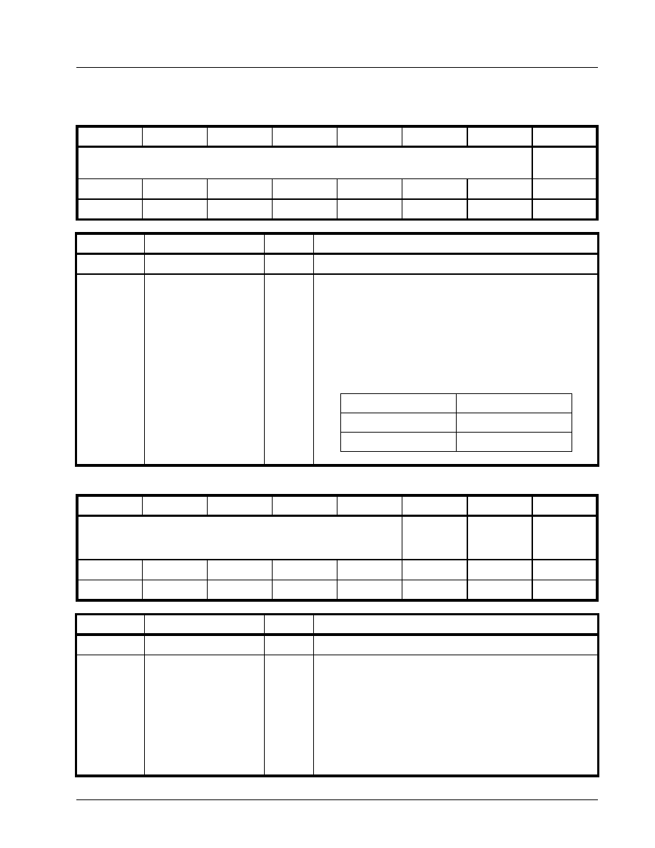
·Á
·Á
·Á
·Á
PRELIMINARY
XRT79L71
1 - CHANNEL DS3/E3 ATM UNI/PPP COMBO IC
REV. P1.0.3
77
OPERATION BLOCK INTERRUPT REGISTER BIT FORMATS
OPERATION CONTROL REGISTER - BYTE 3 (ADDRESS = 0X0100)
B
IT
7
B
IT
6
B
IT
5
B
IT
4
B
IT
3
B
IT
2
B
IT
1
B
IT
0
Unused
Configuration
Control
R/O
R/O
R/O
R/O
R/O
R/O
R/O
R/O
0
0
0
0
0
0
0
0
B
IT
N
UMBER
N
AME
T
YPE
D
ESCRIPTION
7 - 6
Unused
R/O
0
Configuration Control
R/W
Configuration Control:
This READ/WRITE bit-field permits the user to configure the
XRT79L71 device to support any of the following configurations.
∑
ATM/PPP
∑
Clear Channel/HDLC
The following table presents the relationship between the value
written into these register bits and the corresponding Mode of
operation.
OPERATION CONTROL REGISTER - BYTE 2 (ADDRESS = 0X0101)
B
IT
7
B
IT
6
B
IT
5
B
IT
4
B
IT
3
B
IT
2
B
IT
1
B
IT
0
Unused
Interrupt
WC/INT*
Enable
Interrupt
Auto-Clear
Interrupt
Enable
R/O
R/O
R/O
R/O
R/O
R/W
R/W
R/W
0
0
0
0
0
0
0
0
B
IT
N
UMBER
N
AME
T
YPE
D
ESCRIPTION
7 - 3
Unused
R/O
Please set to "0" for normal operation.
2
Interrupt Write to Clear/
RUR
R/W
Interrupt - Write to Clear/RUR Select:
This READ/WRITE bit-field permits the user to configure all of
the "Source-Level" Interrupt Status bits (within the XRT79L71
device) to either be "Write to Clear" (WTC) or "Reset-upon-
Read" (RUR) bits.
0 - Configures all "Source-Level" Interrupt Status register bits to
function as "Reset-upon-Read" (RUR).
1 - Configures all "Source-Level" Interrupt Status register bits to
function as "Write-to-Clear" (WTC).
C o n fig u ra tio n C o n tro l
M o d e
A TM /P P P
C lear C ha nnel/H D LC
0
1

XRT79L71
PRELIMINARY
·Á
·Á
·Á
·Á
REV. P1.0.3
1 - CHANNEL DS3/E3 ATM UNI/PPP COMBO IC
78
1
Enable Interrupt Clear
R/W
Enable Auto-Clear of Interrupts Select:
This READ/WRITE bit-field permits the user to configure the
XRT79L71 device to automatically disable all interrupts that are
activated.
0 - Configures the chip to NOT automatically disable any Inter-
rupts following their activation.
1 - Configures the chip to automatically disable all Interrupts fol-
lowing their activation.
0
Interrupt Enable
R/W
Interrupt Enable:
This READ/WRITE bit-field permits the user to configure the
XRT79L71 device to generate interrupt requests to the Micropro-
cessor.
0 - Configures the chip to NOT generate interrupt to the Micro-
processor. All interrupts are disabled and the Microprocessor
must poll the register bits.
1 - Configures the chip to generate interrupts the Microproces-
sor.
OPERATION CONTROL - LOOP-BACK CONTROL REGISTER (ADDRESS = 0X0102)
B
IT
7
B
IT
6
B
IT
5
B
IT
4
B
IT
3
B
IT
2
B
IT
1
B
IT
0
Unused
Loop-back Control [3:0]
R/O
R/O
R/O
R/O
R/W
R/W
R/W
R/W
0
0
0
0
0
0
0
0
B
IT
N
UMBER
N
AME
T
YPE
D
ESCRIPTION
7 - 4
Unused
R/O
3 - 0
Loop-back Control [3:0]
R/W
Loop-back Mode Select:
These READ/WRITE bit-fields permit the user to configure the
XRT79L71 to operate in any of the following loop-back modes.
∑
Local Medium Loop-back
∑
Remote Host Loop-back
The following table presents the contents of these bit-fields and
the corresponding Loop-back Modes.
B
IT
N
UMBER
N
AME
T
YPE
D
ESCRIPTION
R eserved
R em ote H o st Loop-back M ode
Local M edium Loop-back M ode
R eserved
R e s u ltin g L o o p -b a c k M o d e
0110 - 111 1
0101
0100
0000 - 001 1
L o o p -b a c k C o n tro l [3 :0 ]
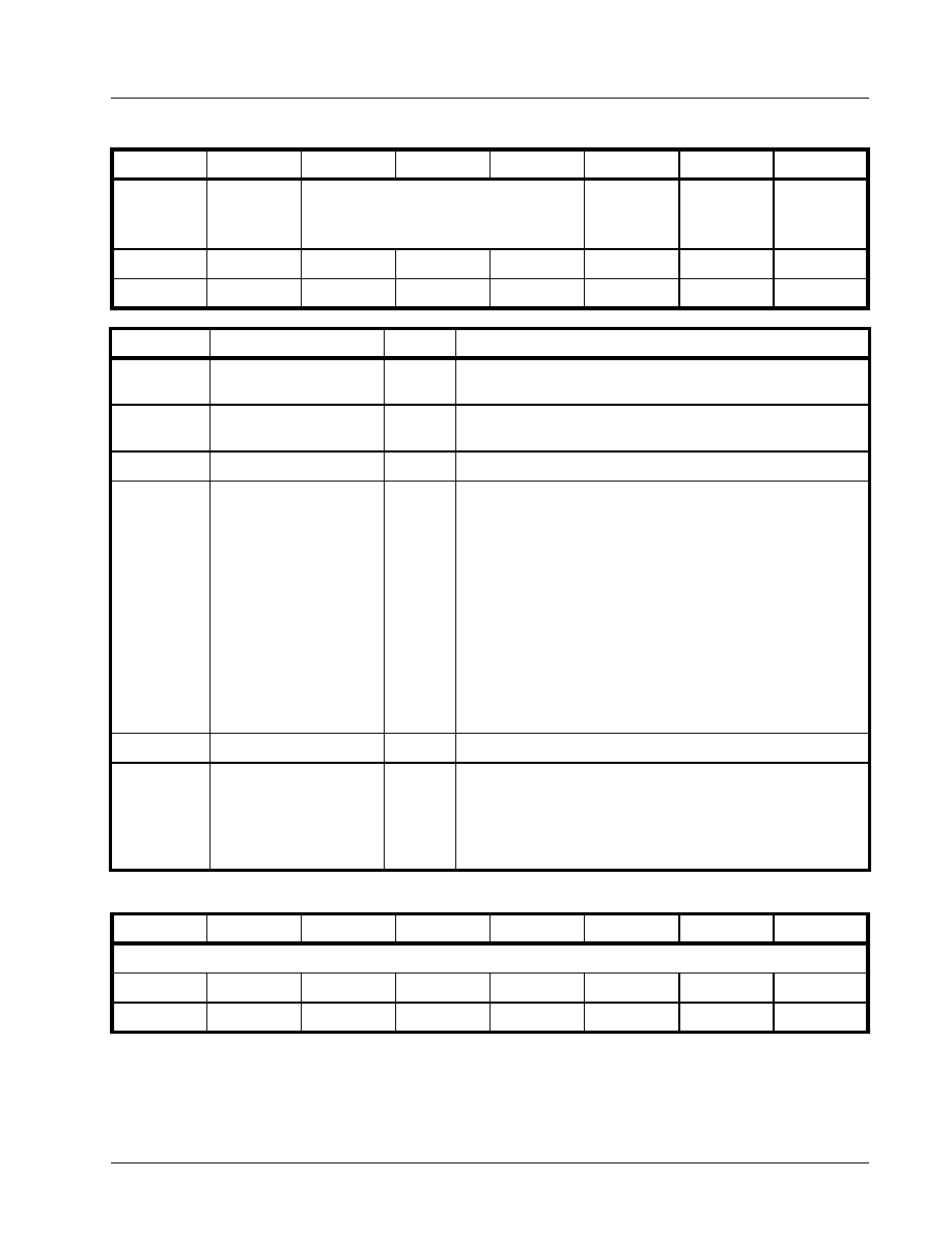
·Á
·Á
·Á
·Á
PRELIMINARY
XRT79L71
1 - CHANNEL DS3/E3 ATM UNI/PPP COMBO IC
REV. P1.0.3
79
OPERATION CONTROL REGISTER - BYTE 0 (ADDRESS = 0X0103)
B
IT
7
B
IT
6
B
IT
5
B
IT
4
B
IT
3
B
IT
2
B
IT
1
B
IT
0
Transmit
UTOPIA
PLL OFF
Receive
UTOPIA
PLL OFF
Reserved
PPP/ATM*
Reserved
Software
RESET*
R/W
R/W
R/W
R/W
R/W
R/W
R/W
R/W
0
0
0
0
0
0
0
0
B
IT
N
UMBER
N
AME
T
YPE
D
ESCRIPTION
7
Transmit UTOPIA PLL
OFF
R/W
6
Receive UTOPIA PLL
OFF
R/W
5 - 3
Unused
R/O
2
PPP/ATM*
R/W
PPP/ATM UNI Mode Select:
This READ-WRITE bit-field permits the user to configure the
XRT79L71 device to operate in either the ATM UNI or PPP
Mode.
If Bit 3 (Dual Bus), within the "Operation Control Register - Byte
3" is set to "0", then this bit-field will then dictate the operating
mode of the XRT79L71 device.
0 - Configures the "Dedicated" UTOPIA/POS-PHY bus to oper-
ate in the UTOPIA (ATM) Mode.
1 - Configures the "Dedicated" UTOPIA/POS-PHY Bus to oper-
ate in the POS-PHY Mode.
N
OTE
: This bit-field is ignored if Bit 3 (Dual-Bus) within the
"Operation Control Register - Byte 3" is set to "1".
1
Reserved
R/O
0
Software RESET
R/W
Software RESET:
This READ-WRITE bit-field permits the user to reset the
XRT79L71 device.
0 - Configure the XRT79L71 device into RESET mode.
1 - Normal operation.
DEVICE ID REGISTER (ADDRESS = 0X0104)
B
IT
7
B
IT
6
B
IT
5
B
IT
4
B
IT
3
B
IT
2
B
IT
1
B
IT
0
DEVICE_ID_VALUE [7:0]
R/O
R/O
R/O
R/O
R/O
R/O
R/O
R/O
0
1
1
1
1
0
1
0
XRT79L71
PRELIMINARY
·Á
·Á
·Á
·Á
REV. P1.0.3
1 - CHANNEL DS3/E3 ATM UNI/PPP COMBO IC
80
B
IT
N
UMBER
N
AME
T
YPE
D
ESCRIPTION
7 - 0
Device ID Value
R/O
Device ID Value:
This READ-ONLY bit-field is set to the value "0x7A" and permits
the user's software code to uniquely identify this device as the
XRT79L71 device.
REVISION ID REGISTER (ADDRESS = 0X0105)
B
IT
7
B
IT
6
B
IT
5
B
IT
4
B
IT
3
B
IT
2
B
IT
1
B
IT
0
Revision Number Value
R/O
R/O
R/O
R/O
R/O
R/O
R/O
R/O
0
0
0
0
0
0
0
1
B
IT
N
UMBER
N
AME
T
YPE
D
ESCRIPTION
7 - 0
Revision Number Value
R/O
Revision Number Value:
This READ-ONLY bit-field is set to the value that corresponds to
its revision number. Revision A silicon will be set to the value
"0x01". This register permits the user's software code to
uniquely identify the revision number of the XRT79L71 device.
OPERATION INTERRUPT STATUS REGISTER - BYTE 1 (ADDRESS = 0X0112)
B
IT
7
B
IT
6
B
IT
5
B
IT
4
B
IT
3
B
IT
2
B
IT
1
B
IT
0
Unused
DS3/E3
LIU/JA Block
Interrupt
Status
DS3/E3
Framer Block
Interrupt
Status
Unused
R/O
R/O
R/O
R/O
R/O
R/O
R/O
R/O
0
0
0
0
0
0
0
0
B
IT
N
UMBER
N
AME
T
YPE
D
ESCRIPTION
7 - 4
Unused
R/O
3
DS3/E3 LIU/JA Block
Interrupt Status
R/O
DS3/E3 LIU/JA Block Interrupt Status:
This READ-ONLY bit-field indicates whether or not a "DS3/E3
LIU/JA Block" interrupt is awaiting service.
0 - No "DS3/E3 LIU/JA" block interrupt is awaiting service.
1 - At least one "DS3/E3 LIU/JA" block interrupt is awaiting ser-
vice.
2
DS3/E3 Framer Block
Interrupt Status
R/O
DS3/E3 Framer Block Interrupt Status:
This READ-ONLY bit-field indicates whether or not a "DS3/E3
Framer Block" interrupt is awaiting service.
0 - No "DS3/E3 Framer" block interrupt is awaiting service.
1 - At least one "DS3/E3 Framer" block interrupt is awaiting ser-
vice.
1 - 0
Unused
R/O

·Á
·Á
·Á
·Á
PRELIMINARY
XRT79L71
1 - CHANNEL DS3/E3 ATM UNI/PPP COMBO IC
REV. P1.0.3
81
OPERATION INTERRUPT STATUS REGISTER - BYTE 0 (ADDRESS = 0X0113)
B
IT
7
B
IT
6
B
IT
5
B
IT
4
B
IT
3
B
IT
2
B
IT
1
B
IT
0
Receive
UTOPIA/
POS-PHY
Interface
Block
Interrupt
Status
Unused
Receive
ATM Cell/PPP
Processor
Block
Interrupt
Status
Transmit
UTOPIA/
POS-PHY
Interface
Block
Interrupt
Status
Unused
Transmit
ATM Cell/PPP
Processor
Block
Interrupt
Status
R/O
R/O
R/O
R/O
R/O
R/O
R/O
R/O
0
0
0
0
0
0
0
0
B
IT
N
UMBER
N
AME
T
YPE
D
ESCRIPTION
7
Receive UTOPIA
POS-PHY Interface Block
Interrupt Status
R/O
Receive UTOPIA/POS-PHY Interface Block Interrupt Status:
This READ-ONLY bit-field indicates whether or not a "Receive
UTOPIA/POS-PHY Interface" block interrupt is awaiting service.
0 - No "Receive UTOPIA/POS-PHY Interface" block interrupt is
awaiting service.
1 - At least one "Receive UTOPIA/POS-PHY Interface" block
interrupt is awaiting service.
6 -5
Unused
R/O
4
Receive ATM Cell/PPP
Processor Block
Interrupt Status
R/O
Receive ATM Cell/PPP Processor Block Interrupt Status:
This READ-ONLY bit-field indicates whether or not a "Receive
ATM Cell/PPP Processor Block" Interrupt is awaiting service.
0 - No "Receive ATM Cell/PPP Processor block" interrupt is
awaiting service.
1 - At least one "Receive ATM Cell/PPP Processor" block inter-
rupt is awaiting service.
3
Transmit UTOPIA
POS-PHY Interface Block
Interrupt Status
Transmit UTOPIA/POS-PHY Interface Block Interrupt Status:
This READ-ONLY bit-field indicates whether or not a "Transmit
UTOPIA/POS-PHY Interface" block interrupt is awaiting service.
0 - No "Transmit UTOPIA/POS-PHY Interface" block interrupt is
awaiting service.
1 - At least one "Transmit UTOPIA/POS-PHY Interface" block
interrupt is awaiting service.
2 - 1
Unused
R/O
0
Transmit ATM Cell/PPP
Processor Block
Interrupt Status
R/O
Receive ATM Cell/PPP Processor Block Interrupt Status:
This READ-ONLY bit-field indicates whether or not a "Receive
ATM Cell/PPP Processor Block" Interrupt is awaiting service.
0 - No "Receive ATM Cell/PPP Processor block" interrupt is
awaiting service.
1 - At least one "Receive ATM Cell/PPP Processor" block inter-
rupt is awaiting service.

XRT79L71
PRELIMINARY
·Á
·Á
·Á
·Á
REV. P1.0.3
1 - CHANNEL DS3/E3 ATM UNI/PPP COMBO IC
82
OPERATION INTERRUPT ENABLE REGISTER - BYTE 1 (ADDRESS = 0X0116)
B
IT
7
B
IT
6
B
IT
5
B
IT
4
B
IT
3
B
IT
2
B
IT
1
B
IT
0
Unused
DS3/E3
LIU/JA Block
Interrupt
Enable
DS3/E3
Framer Block
Interrupt
Enable
Unused
R/O
R/O
R/O
R/O
R/W
R/W
R/O
R/O
0
0
0
0
0
0
0
0
B
IT
N
UMBER
N
AME
T
YPE
D
ESCRIPTION
7 - 4
Unused
3
DS3/E3 LIU/JA
Block Interrupt Enable
R/W
DS3/E3 LIU/JA Block Interrupt Enable:
This READ/WRITE bit permit the user to either enable or disable
the DS3/E3 LIU/JA Block for interrupt generation. If the user
writes a "0" to this register bit and disables the "DS3/E3 LIU/JA
Block" (for interrupt generation), then all "DS3/E3 LIU/JA Block"
interrupts will be disabled for interrupt generation. If the user
writes a "1" to this register bit, he/she will still need to enable the
individual "DS3/E3 LIU/JA Block" interrupt(s) at the "Source
Level" in order to enable that particular interrupt.
0 - Disable all "DS3/E3 LIU/JA Block" interrupts within the
device.
1 - Enables the "DS3/E3 LIU/JA Block" at the "Block-Level".
2
DS3/E3 Framer Block
Interrupt Enable
R/W
DS3/E3 Framer Block Interrupt Enable:
This READ/WRITE bit permits the user to either enable or dis-
able the DS3/E3 Framer Block for interrupt generation. If the
user writes a "0" to this register bit and disables the "DS3/E3
Framer Block" (for interrupt generation), then all "DS3/E3 Framer
Block" interrupts will be disabled for interrupt generation. If the
user writes a "1" to this register bit, he/she will still need to
enable the individual "DS3/E3 Framer Block" interrupt(s) at the
"Source Level" in order to enable that particular interrupt.
0 - Disable all "DS3/E3 Framer Block" interrupts within the
device.
1 - Enables the "DS3/E3 Framer Block" at the "Block-Level".
1 - 0
Unused

·Á
·Á
·Á
·Á
PRELIMINARY
XRT79L71
1 - CHANNEL DS3/E3 ATM UNI/PPP COMBO IC
REV. P1.0.3
83
OPERATION INTERRUPT ENABLE REGISTER - BYTE 0 (ADDRESS = 0X0117)
B
IT
7
B
IT
6
B
IT
5
B
IT
4
B
IT
3
B
IT
2
B
IT
1
B
IT
0
Receive
UTOPIA/
POS-PHY
Interface
Block
Interrupt
Enable
Unused
Receive
ATM Cell/PPP
Processor
Block
Interrupt
Enable
Transmit
UTOPIA/
POS-PHY
Interface
Block
Interrupt
Enable
Unused
Transmit
ATM Cell/PPP
Processor
Block
Interrupt
Enable
R/W
R/O
R/O
R/W
R/W
R/O
R/O
R/W
0
0
0
0
0
0
0
0
B
IT
N
UMBER
N
AME
T
YPE
D
ESCRIPTION
7
Receive
UTOPIA/POS-PHY
Interface Block Interrupt
Enable
R/W
Receive UTOPIA/POS-PHY Interface Block Interrupt Enable:
This READ/WRITE bit permit the user to either enable or disable
the Receive UTOPIA/POS-PHY Interface Block for interrupt gen-
eration. If the user writes a "0" to this register bit and disables
the "Receive UTOPIA/POS-PHY Interface Block" (for interrupt
generation), then all "Receive UTOPIA/POS-PHY Interface
Block" interrupts will be disabled for interrupt generation. If the
user writes a "1" to this register bit, he/she will still need to
enable the individual "Receive UTOPIA/POS-PHY Interface
Block" interrupt(s) at the "Source Level" in order to enable that
particular interrupt.
0 - Disable all "Receive UTOPIA/POS-PHY Interface Block"
interrupts within the device.
1 - Enables the "Receive UTOPIA/POS-PHY Interface Block" at
the "Block-Level".
6 - 5
Unused
R/O
4
Receive
ATM Cell/PPP Processor
Block Interrupt Enable
R/W
Receive ATM Cell/PPP Processor Block Interrupt Enable:
This READ/WRITE bit permit the user to either enable or disable
the Receive ATM Cell/PPP Processor Block for interrupt genera-
tion. If the user writes a "0" to this register bit and disables the
"Receive ATM Cell/PPP Processor Block" (for interrupt genera-
tion), then all "Receive ATM Cell/PPP Processor Block" inter-
rupts will be disabled for interrupt generation. If the user writes a
"1" to this register bit, he/she will still need to enable the individ-
ual "Receive ATM Cell/PPP Processor Block" interrupt(s) at the
"Source Level" in order to enable that particular interrupt.
0 - Disable all "Receive ATM Cell/PPP Processor Block" inter-
rupts within the device.
1 - Enables the "Receive ATM Cell/PPP Processor Block" at the
"Block-Level".

XRT79L71
PRELIMINARY
·Á
·Á
·Á
·Á
REV. P1.0.3
1 - CHANNEL DS3/E3 ATM UNI/PPP COMBO IC
84
CHANNEL INTERRUPT INDICATION REGISTERS
3
Transmit
UTOPIA/POS-PHY
Interface Block Interrupt
Enable
R/W
Transmit UTOPIA/POS-PHY Interface Block Interrupt
Enable:
This READ/WRITE bit permit the user to either enable or disable
the Transmit UTOPIA/POS-PHY Interface Block for interrupt
generation. If the user writes a "0" to this register bit and dis-
ables the "Transmit UTOPIA/POS-PHY Interface Block" (for
interrupt generation), then all "Transmit UTOPIA/POS-PHY Inter-
face Block" interrupts will be disabled for interrupt generation. If
the user writes a "1" to this register bit, he/she will still need to
enable the individual "Transmit UTOPIA/POS-PHY Interface
Block" interrupt(s) at the "Source Level" in order to enable that
particular interrupt.
0 - Disable all "Transmit UTOPIA/POS-PHY Interface Block"
interrupts within the device.
1 - Enables the "Transmit UTOPIA/POS-PHY Interface Block" at
the "Block-Level".
2 - 1
Unused
R/O
0
Transmit ATM Cell/PPP
Processor Block
Interrupt Enable
R/W
Transmit ATM Cell/PPP Processor Block Interrupt Enable:
This READ/WRITE bit permit the user to either enable or disable
the Transmit ATM Cell/PPP Processor Block for interrupt genera-
tion. If the user writes a "0" to this register bit and disables the
"Transmit ATM Cell/PPP Processor Block" (for interrupt genera-
tion), then all "Transmit ATM Cell/PPP Processor Block" inter-
rupts will be disabled for interrupt generation. If the user writes a
"1" to this register bit, he/she will still need to enable the individ-
ual "Transmit ATM Cell/PPP Processor Block" interrupt(s) at the
"Source Level" in order to enable that particular interrupt.
0 - Disable all "Transmit ATM Cell/PPP Processor Block" inter-
rupts within the device.
1 - Enables the "Transmit ATM Cell/PPP Processor Block" at the
"Block-Level".
CHANNEL INTERRUPT INDICATOR - RECEIVE CELL PROCESSOR/PPP PROCESSOR BLOCK
(ADDRESS = 0X0119)
B
IT
7
B
IT
6
B
IT
5
B
IT
4
B
IT
3
B
IT
2
B
IT
1
B
IT
0
Unused
Receive Cell
Processor
Block
Interrupt
R/O
R/O
0
0
B
IT
N
UMBER
N
AME
T
YPE
D
ESCRIPTION
7 - 1
Unused
R/O
B
IT
N
UMBER
N
AME
T
YPE
D
ESCRIPTION
·Á
·Á
·Á
·Á
PRELIMINARY
XRT79L71
1 - CHANNEL DS3/E3 ATM UNI/PPP COMBO IC
REV. P1.0.3
85
0
Receive Cell Processor
Block Interrupt -
XRT79L71
R/O
Receive Cell Processor Block Interrupt - XRT79L71:
This READ/ONLY bit-field indicates whether or not the "Receive
Cell Processor" block, associated with XRT79L71 is declaring an
Interrupt, as described below.
0 - The Receive Cell Processor block, associated with
XRT79L71 is NOT declaring an Interrupt.
1 - The Receive Cell Processor block, associated with
XRT79L71 is currently declaring an interrupt.
CHANNEL INTERRUPT INDICATOR - LIU/JITTER ATTENUATOR BLOCK (ADDRESS = 0X011D)
B
IT
7
B
IT
6
B
IT
5
B
IT
4
B
IT
3
B
IT
2
B
IT
1
B
IT
0
Unused
LIU/JA Block
Interrupt
R/O
R/O
0
0
B
IT
N
UMBER
N
AME
T
YPE
D
ESCRIPTION
7 - 1
Unused
R/O
0
LIU/JA Block Interrupt -
XRT79L71
R/O
LIU/JA Block Interrupt - XRT79L71:
This READ/ONLY bit-field indicates whether or not the "LIU/JA"
block, associated with XRT79L71 is declaring an Interrupt, as
described below.
0 - The LIU/JA block, associated with XRT79L71 is NOT declar-
ing an Interrupt.
1 - The LIU/JA block, associated with XRT79L71 is currently
declaring an interrupt.
CHANNEL INTERRUPT INDICATOR - TRANSMIT CELL PROCESSOR/PPP PROCESSOR BLOCK
(ADDRESS = 0X0121)
B
IT
7
B
IT
6
B
IT
5
B
IT
4
B
IT
3
B
IT
2
B
IT
1
B
IT
0
Unused
Transmit Cell
Processor
Block
Interrupt
R/O
R/O
0
B
IT
N
UMBER
N
AME
T
YPE
D
ESCRIPTION
7 - 1
Unused
R/O
B
IT
N
UMBER
N
AME
T
YPE
D
ESCRIPTION
XRT79L71
PRELIMINARY
·Á
·Á
·Á
·Á
REV. P1.0.3
1 - CHANNEL DS3/E3 ATM UNI/PPP COMBO IC
86
0
Transmit Cell Processor
Block Interrupt -
XRT79L71
R/O
Transmit Cell Processor Block Interrupt - XRT79L71:
This READ/ONLY bit-field indicates whether or not the "Transmit
Cell Processor" block, associated with XRT79L71 is declaring an
Interrupt, as described below.
0 - The Transmit Cell Processor block, associated with
XRT79L71 is NOT declaring an Interrupt.
1 - The Transmit Cell Processor block, associated with
XRT79L71 is currently declaring an interrupt.
CHANNEL INTERRUPT INDICATOR - DS3/E3 FRAMER BLOCK (ADDRESS = 0X0127)
B
IT
7
B
IT
6
B
IT
5
B
IT
4
B
IT
3
B
IT
2
B
IT
1
B
IT
0
Unused
DS3/E3
Framer Block
Interrupt
R/O
R/O
0
0
B
IT
N
UMBER
N
AME
T
YPE
D
ESCRIPTION
7 - 1
Unused
R/O
0
DS3/E3 Framer Block
Interrupt - XRT79L71
R/O
DS3/E3 Framer Block Interrupt - XRT79L71:
This READ/ONLY bit-field indicates whether or not the "DS3/E3
Framer" block, associated with XRT79L71 is declaring an Inter-
rupt, as described below.
0 - The DS3/E3 Framer block, associated with XRT79L71 is NOT
declaring an Interrupt.
1 - The DS3/E3 Framer block, associated with XRT79L71 is cur-
rently declaring an interrupt.
OPERATION GENERAL PURPOSE PIN DATA REGISTER (ADDRESS = 0X0147)
B
IT
7
B
IT
6
B
IT
5
B
IT
4
B
IT
3
B
IT
2
B
IT
1
B
IT
0
Unused
General
Purpose
Data [3]
General
Purpose
Data [2]
General
Purpose
Data [1]
General
Purpose
Data [0]
R/O
R/W
R/W
R/W
R/W
0
0
0
0
0
OPERATION GENERAL PURPOSE PIN DIRECTION CONTROL REGISTER (ADDRESS = 0X014B)
B
IT
7
B
IT
6
B
IT
5
B
IT
4
B
IT
3
B
IT
2
B
IT
1
B
IT
0
Unused
General
Purpose Pin
Direction [3]
General
Purpose Pin
Direction [2]
General
Purpose Pin
Direction [1]
General
Purpose Pin
Direction [0]
R/O
R/W
R/W
R/W
R/W
0
0
0
0
0
B
IT
N
UMBER
N
AME
T
YPE
D
ESCRIPTION

·Á
·Á
·Á
·Á
PRELIMINARY
XRT79L71
1 - CHANNEL DS3/E3 ATM UNI/PPP COMBO IC
REV. P1.0.3
87
RECEIVE UTOPIA INTERFACE BLOCK
This section presents the Register Description/Address Map of the control registers associated with the
Receive UTOPIA/POS-PHY Interface block.
T
ABLE
15: R
ECEIVE
UTOPIA/POS-PHY I
NTERFACE
B
LOCK
- R
EGISTER
/A
DDRESS
M
AP
A
DDRESS
L
OCATION
R
EGISTER
N
AME
T
YPE
D
EFAULT
V
ALUE
R
ECEIVE
UTOPIA/POS-PHY- C
ONTROL
R
EGISTERS
0x0501
Receive UTOPIA/POS-PHY Control Register - Byte 2
R/W
0x00
0x0502
Receive UTOPIA/POS-PHY Control Register - Byte 1
R/W
0x00
0x0503
Receive UTOPIA/POS-PHY Control Register - Byte 0
R/W
0x00
0x0504 - 0x0512
Reserved
R/O
0x00
0x0513
Receive UTOPIA Port Address Register
R/W
0x00
0x0514 - 0x0516
Reserved
R/O
0x00
0x0517
Receive UTOPIA Port Number Register
R/W
0x00
0x0518 - 0x0580
Reserved
R/O
0x00
RECEIVE UTOPIA/POS-PHY CONTROL REGISTER - BYTE 0 (ADDRESS = 0X0503)
B
IT
7
B
IT
6
B
IT
5
B
IT
4
B
IT
3
B
IT
2
B
IT
1
B
IT
0
UTOPIA
Level 3
Disable
Multi-PHY
Polling Enable
Back to Back
Polling Enable
Direct Status
Indication
Enable
UTOPIA/POS-PHY
Data Bus Width
Cell Size[1:0]
R/W
R/W
R/W
R/W
R/W
R/W
R/W
R/W
1
1
0
0
1
1
1
1
B
IT
N
UMBER
N
AME
T
YPE
D
ESCRIPTION
7
UTOPIA Level 3 Disable
R/W
6
Multi-PHY Polling Enable
R/W
Multi-PHY Polling Enable:
This READ/WRITE bit-field permits the user to either enable or
disable Multi-PHY Polling for the Receive UTOPIA Interface
block. If the user implements this feature (and configures the
XRT79L71 device to operate in the Multi-PHY Mode) then the
RxUClav output pin will be driven (either "high" or "low") based
upon the fill-status of the Receive FIFO within the Channel that
corresponds to the "Receive UTOPIA Address" that is currently
being applied to the "RxUAddr[4:0]" input pins.
If the user does not implement this feature (and then configures
the XRT79L71 device to operate in the Single-PHY Mode), then
the "RxUClav" output pin will unconditionally reflect the "Receive
FIFO fill-status" for Channel 0. No attention will be paid to the
address values placed upon the "RxUAddr[4:0]" input pins.
0 - Configures the Receive UTOPIA Interface block to operate in
the Single-PHY Mode.
1 - Configures the Receive UTOPIA Interface block to operate in
the Multi-PHY Mode.

XRT79L71
PRELIMINARY
·Á
·Á
·Á
·Á
REV. P1.0.3
1 - CHANNEL DS3/E3 ATM UNI/PPP COMBO IC
88
5
Back-to-Back Polling
Enable
R/W
Back-to-Back Polling Enable:
This READ/WRITE bit-field permits the user to configure the
Receive UTOPIA Interface block to support "Back-to-Back Poll-
ing".
Ordinarily, for Multi-PHY polling, the user is required to interleave
all UTOPIA Address values (that are to be placed on the "RxU-
Addr[4:0]" input pins) with the NULL Address (e.g., 0x1F). How-
ever, if the user configures the Receive UTOPIA Interface block
to operate in the "UTOPIA Level 3" Mode, and if the user also
enables "Back-to-Back Polling", then he/she does not need inter-
leave the UTOPIA Addresses with the NULL Address. In this
case, the user can simply apply a "back-to-back" stream of "rele-
vant" UTOPIA Addresses to the "RxUAddr[4:0]" input pins, and
the XRT79L71 device will respond by driving the RxUClav output
pins to the appropriate states (depending upon the Receive
FIFO fill-status).
0 - Disables "Back-to-Back" Polling. In this mode, the user must
interleave all UTOPIA Addresses (that are to be applied to the
"RxUAddr[4:0]" input pins) with the NULL Address.
1 - Enables "Back-to-Back" Polling. In this mode, the user does
not need to interleave all UTOPIA Addresses (that are to be
applied to the "RxUAddr[4:0]" input pins) with the NULL Address.
N
OTE
: In order to configure the Receive UTOPIA Interface block
to operate in the "Back-to-Back Polling" Mode, the user
must also do the following.
a. Configure the Receive UTOPIA Interface to operate in the
"UTOPIA Level 3" Mode. This is accomplished by setting
Bit 7 (UTOPIA Level 3 Disable) within this Register to "0".
b. Configure the Receive UTOPIA Interface to support "Multi-
PHY" Polling. This is accomplished by setting Bit 6 (Multi-
PHY Polling Enable) within this register to "1".
4
Direct Status Indication
Enable
R/W
3 - 2
UTOPIA/POS-PHY
Data Bus Width[1:0]
R/W
UTOPIA/POS-PHY Data Bus Width[1:0]:
These READ/WRITE bit-fields permit the user to select the width
of the Receive UTOPIA and POS-PHY Data Buses. The rela-
tionship between the contents of these bit-fields and the corre-
sponding widths of the Receive UTOPIA and POS-PHY Data
Bus is tabulated below.
B
IT
N
UMBER
N
AME
T
YPE
D
ESCRIPTION
1
1
0
1
1
0
0
0
N ot V alid
16 bits
8 bits
N ot V alid
C o rre s p o n d in g
U T O P IA /P O S -P H Y
D a ta B u s W id th
U T O P IA /P O S -P H Y
D a ta B u s
W id th [1 :0 ]
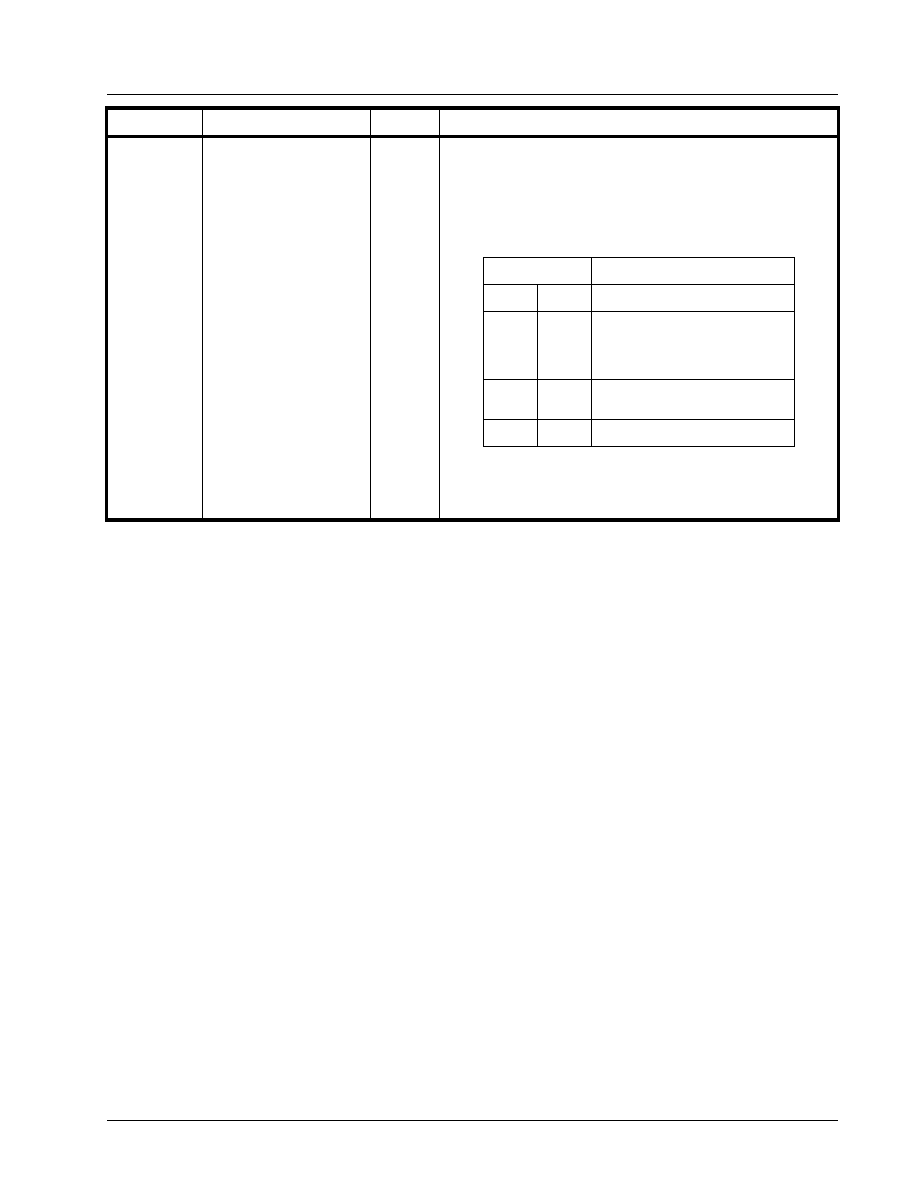
·Á
·Á
·Á
·Á
PRELIMINARY
XRT79L71
1 - CHANNEL DS3/E3 ATM UNI/PPP COMBO IC
REV. P1.0.3
89
1 - 0
Cell Size[1:0]
Cell Size[1:0]:
These two READ/WRITE bit-fields permit the user to specify the
size of the ATM cell that will be handled by the Receive UTOPIA
Interface blocks. The relationship between the contents of these
bit-fields and the corresponding Cell Sizes are tabulated below.
N
OTE
: The user must bear in mind the UTOPIA Level and the
UTOPIA Data Bus width selected, when selecting the
Cell Size.
B
IT
N
UMBER
N
AME
T
YPE
D
ESCRIPTION
1
1
0
1
1
0
0
0
56 bytes
54 bytes (O nly valid for
U TO P IA Levels 1 and 2)
53 bytes (O nly valid for
U TO P IA Level 1, and if the
U TO P IA D ata B us W idth is set
to 8 bits)
52 bytes
R e s u ltin g C e ll S iz e (B yte s )
C e ll S iz e [1 :0 ]
XRT79L71
PRELIMINARY
·Á
·Á
·Á
·Á
REV. P1.0.3
1 - CHANNEL DS3/E3 ATM UNI/PPP COMBO IC
90
RECEIVE UTOPIA PORT ADDRESS REGISTER (ADDRESS = 0X0513)
B
IT
7
B
IT
6
B
IT
5
B
IT
4
B
IT
3
B
IT
2
B
IT
1
B
IT
0
Unused
Receive UTOPIA Port Address[4:0]
R/O
R/O
R/O
R/W
R/W
R/W
R/W
R/W
0
0
0
0
0
0
0
0
B
IT
N
UMBER
N
AME
T
YPE
D
ESCRIPTION
7 - 5
Unused
R/O
4 - 0
Receive UTOPIA Port
Address[4:0]
R/W
Receive UTOPIA Port Address[4:0]:
These READ/WRITE register bits, along with the "Receive UTO-
PIA Port Number[4:0]" bits (within the "Receive UTOPIA Port
Number" Register (Address = 0x0517) permit the user to assign
a unique Receive UTOPIA address to each of the XRT79L71
device.
For UTOPIA Level 2/3 applications, the user can write in any
value, ranging from 0x00 through 0x1E into this register.
The Receive UTOPIA Address Assignment Procedure:
In order to assign a UTOPIA Address to a given Channel (or
Port) within the XRT79L71 device, the user must do the follow-
ing.
a. Write the value corresponding to a given XRT79L71
Channel into the "Receive UTOPIA Port Number" Register
(Address = 0x0517).
b. Write the corresponding UTOPIA Address value into this
register.
Once this "two-step" procedure has been executed, then the
XRT79L71 Channel (as specified during step "a") will be
assigned the "Receive UTOPIA Address" value (as specified
during step "b").
RECEIVE UTOPIA PORT NUMBER REGISTER (ADDRESS = 0X0517)
B
IT
7
B
IT
6
B
IT
5
B
IT
4
B
IT
3
B
IT
2
B
IT
1
B
IT
0
Unused
Receive UTOPIA Port Number[4:0]
R/O
R/O
R/O
R/W
R/W
R/W
R/W
R/W
0
0
0
0
0
0
0
0
B
IT
N
UMBER
N
AME
T
YPE
D
ESCRIPTION
7 - 5
Unused
R/O

·Á
·Á
·Á
·Á
PRELIMINARY
XRT79L71
1 - CHANNEL DS3/E3 ATM UNI/PPP COMBO IC
REV. P1.0.3
91
4 - 0
Receive UTOPIA Port
Number[4:0]
R/W
Receive UTOPIA Port Number[4:0]:
These READ/WRITE register bits, along with the "Receive UTO-
PIA Port Address[4:0]" bits (within the "Receive UTOPIA Port
Address" Register (Address = 0x0513) permit the user to assign
a unique Receive UTOPIA address to the XRT79L71 device.
The Receive UTOPIA Address Assignment Procedure:
In order to assign a UTOPIA Address to a given Channel (or
Port) within the XRT79L71 device, the user must do the follow-
ing.
a. Write the value corresponding to a given XRT79L71
Channel into this register.
b. Write the corresponding UTOPIA Address value into the
"Receive UTOPIA Port Address" Register (Address =
0x0513).
Once this "two-step" procedure has been executed, then the
XRT79L71 Channel (as specified during step "a") will be
assigned the "Receive UTOPIA Address" value (as specified
during step "b").
B
IT
N
UMBER
N
AME
T
YPE
D
ESCRIPTION
XRT79L71
PRELIMINARY
·Á
·Á
·Á
·Á
REV. P1.0.3
1 - CHANNEL DS3/E3 ATM UNI/PPP COMBO IC
92
TRANSMIT UTOPIA INTERFACE BLOCK
This section presents the Register Description/Address Map of the control registers associated with the
Transmit UTOPIA/POS-PHY Interface blocks.
T
ABLE
16: T
RANSMIT
UTOPIA I
NTERFACE
B
LOCK
- R
EGISTER
/A
DDRESS
M
AP
A
DDRESS
L
OCATION
R
EGISTER
N
AME
T
YPE
D
EFAULT
V
ALUE
T
RANSMIT
UTOPIA/POS-PHY C
ONTROL
R
EGISTERS
0x0581
Transmit UTOPIA/POS-PHY Control Register - Byte 2
R/W
0x38
0x0582
Transmit UTOPIA/POS-PHY Control Register - Byte 1
R/W
0x00
0x0583
Transmit UTOPIA/POS-PHY Control Register - Byte 0
R/W
0x00
0x0584 - 0x0592
Reserved
R/O
0x00
0x0593
Transmit UTOPIA Port Address Register
R/W
0x00
0x0594 - 0x0596
Reserved
R/O
0x00
0x0597
Transmit UTOPIA Port Number Register
R/W
0x00
0x0598 - 0x10FF
Reserved
R/O
0x00
TRANSMIT UTOPIA/POS-PHY CONTROL REGISTER - BYTE 0 (ADDRESS = 0X0583)
B
IT
7
B
IT
6
B
IT
5
B
IT
4
B
IT
3
B
IT
2
B
IT
1
B
IT
0
UTOPIA
Level 3
Disable
Multi-PHY
Polling Enable
Back to Back
Polling Enable
Direct Status
Indication
Enable
UTOPIA/POS-PHY Data Bus
Width
Cell Size[1:0]
R/W
R/W
R/W
R/W
R/W
R/W
R/W
R/W
1
1
0
0
1
1
1
1
B
IT
N
UMBER
N
AME
T
YPE
D
ESCRIPTION
7
UTOPIA Level 3 Disable
R/W
6
Multi-PHY Polling Enable
R/W
Multi-PHY Polling Enable:
This READ/WRITE bit-field permits the user to either enable or
disable Multi-PHY Polling for the Transmit UTOPIA Interface
block. If the user implements this feature (and configures the
XRT79L71 device to operate in the Multi-PHY Mode) then the
TxUClav output pin will be driven (either "high" or "low") based
upon the fill-status of the Transmit FIFO within the Channel that
corresponds to the "Transmit UTOPIA Address" that is currently
being applied to the "TxUAddr[4:0]" input pins.
If the user does not implement this feature (and then configures
the XRT79L71 device to operate in the Single-PHY Mode), then
the "TxUClav" output pin will unconditionally reflect the "Transmit
FIFO fill-status" for Channel 0. No attention will be paid to the
address values placed upon the "TxUAddr[4:0]" input pins.
0 - Configures the Transmit UTOPIA Interface block to operate in
the Single-PHY Mode.
1 - Configures the Transmit UTOPIA Interface block to operate in
the Multi-PHY Mode.

·Á
·Á
·Á
·Á
PRELIMINARY
XRT79L71
1 - CHANNEL DS3/E3 ATM UNI/PPP COMBO IC
REV. P1.0.3
93
5
Back-to-Back Polling
Enable
R/W
Back-to-Back Polling Enable:
This READ/WRITE bit-field permits the user to configure the
Transmit UTOPIA Interface block to support "Back-to-Back Poll-
ing".
Ordinarily, for Multi-PHY polling, the user is required to interleave
all UTOPIA Address values (that are to be placed on the "TxU-
Addr[4:0]" input pins) with the NULL Address (e.g., 0x1F). How-
ever, if the user configures the Transmit UTOPIA Interface block
to operate in the "UTOPIA Level 3" Mode, and if the user also
enables "Back-to-Back Polling", then he/she does not need inter-
leave the UTOPIA Addresses with the NULL Address. In this
case, the user can simply apply a "back-to-back" stream of "rele-
vant" UTOPIA Addresses to the "TxUAddr[4:0]" input pins, and
the XRT79L71 device will respond by driving the TxUClav output
pins to the appropriate states (depending upon the Transmit
FIFO fill-status).
0 - Disables "Back-to-Back" Polling. In this mode, the user must
interleave all UTOPIA Addresses (that are to be applied to the
"TxUAddr[4:0]" input pins) with the NULL Address.
1 - Enables "Back-to-Back" Polling. In this mode, the user does
not need to interleave all UTOPIA Addresses (that are to be
applied to the "TxUAddr[4:0]" input pins) with the NULL Address.
N
OTE
: In order to configure the Transmit UTOPIA Interface block
to operate in the "Back-to-Back Polling" Mode, the user
must also do the following.
a. Configure the Transmit UTOPIA Interface to operate in the
"UTOPIA Level 3" Mode. This is accomplished by setting
Bit 7 (UTOPIA Level 3 Disable) within this Register to "0".
b. Configure the Transmit UTOPIA Interface to support
"Multi-PHY" Polling. This is accomplished by setting Bit 6
(Multi-PHY Polling Enable) within this register to "1".
4
Direct Status Indication
Enable
R/W
3 - 2
UTOPIA/POS-PHY Data
Bus Width[1:0]
R/W
UTOPIA/POS-PHY Data Bus Width[1:0]:
These READ/WRITE bit-fields permit the user to select the width
of the Transmit UTOPIA and POS-PHY Data Buses. The rela-
tionship between the contents of these bit-fields and the corre-
sponding widths of the Transmit UTOPIA and POS-PHY Data
Bus is tabulated below.
B
IT
N
UMBER
N
AME
T
YPE
D
ESCRIPTION
1
1
0
1
1
0
0
0
N ot V alid
16 bits
8 bits
N ot V alid
C o rre s p o n d in g
U T O P IA /P O S -P H Y
D a ta B u s W id th
U T O P IA /P O S -P H Y
D a ta B u s
W id th [1 :0 ]
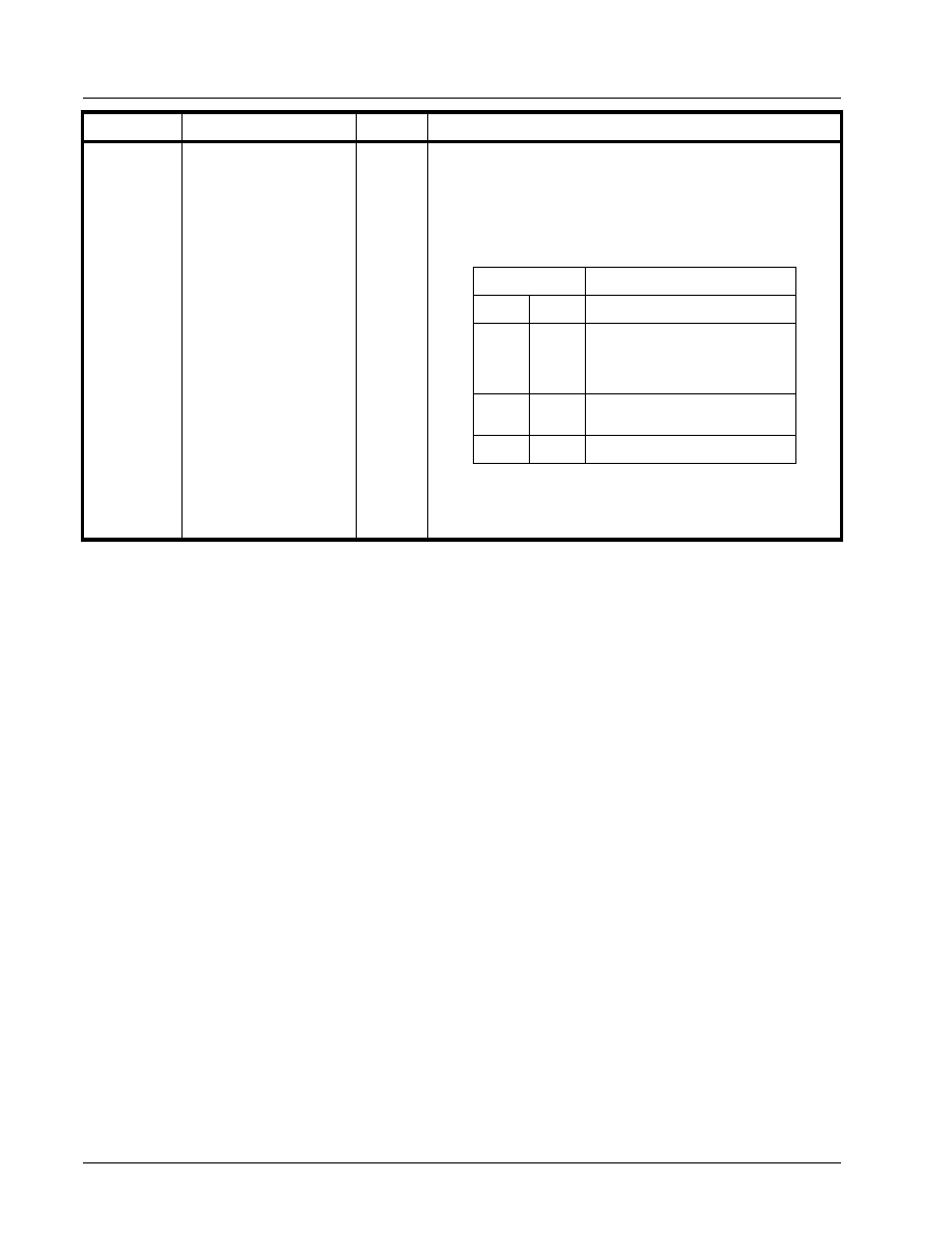
XRT79L71
PRELIMINARY
·Á
·Á
·Á
·Á
REV. P1.0.3
1 - CHANNEL DS3/E3 ATM UNI/PPP COMBO IC
94
1 - 0
Cell Size[1:0]
Cell Size[1:0]:
These two READ/WRITE bit-fields permit the user to specify the
size of the ATM cell that will be handled by the Transmit UTOPIA
Interface blocks. The relationship between the contents of these
bit-fields and the corresponding Cell Sizes are tabulated below.
N
OTE
: The user must bear in mind the UTOPIA Level and the
UTOPIA Data Bus width selected, when selecting the
Cell Size.
B
IT
N
UMBER
N
AME
T
YPE
D
ESCRIPTION
1
1
0
1
1
0
0
0
56 bytes
54 bytes (O nly valid for
U TO P IA Levels 1 and 2)
53 bytes (O nly valid for
U TO P IA Level 1, and if the
U TO P IA D ata B us W idth is set
to 8 bits)
52 bytes
R e s u ltin g C e ll S iz e (B yte s )
C e ll S iz e [1 :0 ]
·Á
·Á
·Á
·Á
PRELIMINARY
XRT79L71
1 - CHANNEL DS3/E3 ATM UNI/PPP COMBO IC
REV. P1.0.3
95
TRANSMIT UTOPIA PORT ADDRESS REGISTER (ADDRESS = 0X0593)
B
IT
7
B
IT
6
B
IT
5
B
IT
4
B
IT
3
B
IT
2
B
IT
1
B
IT
0
Unused
Transmit UTOPIA Port Address[4:0]
R/O
R/O
R/O
R/W
R/W
R/W
R/W
R/W
0
0
0
0
0
0
0
0
B
IT
N
UMBER
N
AME
T
YPE
D
ESCRIPTION
7 - 5
Unused
R/O
4 - 0
Transmit UTOPIA Port
Address[4:0]
R/W
Transmit UTOPIA Port Address[4:0]:
These READ/WRITE register bits, along with the "Transmit UTO-
PIA Port Number[4:0]" bits (within the "Trasnmit UTOPIA Port
Number" Register (Address = 0x0597) permit the user to assign
a unique Transmit UTOPIA address the XRT79L71 device.
For UTOPIA Level 2/3 applications, the user can write in any
value, ranging from 0x00 through 0x1E into this register.
The Transmit UTOPIA Address Assignment Procedure:
In order to assign a UTOPIA Address to a given Channel (or
Port) within the XRT79L71 device, the user must do the follow-
ing.
a. Write the value corresponding to a given XRT79L71
Channel into the "Transmit UTOPIA Port Number"
Register (Address = 0x0597).
b. Write the corresponding UTOPIA Address value into this
register.
Once this "two-step" procedure has been executed, then the
XRT79L71 Channel (as specified during step "a") will be
assigned the "Transmit UTOPIA Address" value (as specified
during step "b").
TRANSMIT UTOPIA PORT NUMBER REGISTER (ADDRESS = 0X0597)
B
IT
7
B
IT
6
B
IT
5
B
IT
4
B
IT
3
B
IT
2
B
IT
1
B
IT
0
Unused
Transmit UTOPIA Port Number[4:0]
R/O
R/O
R/O
R/W
R/W
R/W
R/W
R/W
0
0
0
0
0
0
0
0
B
IT
N
UMBER
N
AME
T
YPE
D
ESCRIPTION
7 - 5
Unused
R/O

XRT79L71
PRELIMINARY
·Á
·Á
·Á
·Á
REV. P1.0.3
1 - CHANNEL DS3/E3 ATM UNI/PPP COMBO IC
96
4 - 0
Transmit UTOPIA Port
Number[4:0]
R/W
Transmit UTOPIA Port Number[4:0]:
These READ/WRITE register bits, along with the "Transmit UTO-
PIA Port Address[4:0]" bits (within the "Transmit UTOPIA Port
Address" Register (Address = 0x0593) permit the user to assign
a unique Transmit UTOPIA address to each XRT79L71 device.
The Transmit UTOPIA Address Assignment Procedure:
In order to assign a UTOPIA Address to a given Channel (or
Port) within the XRT79L71 device, the user must do the follow-
ing.
a. Write the value corresponding to a given XRT79L71
Channel into this register.
b. Write the corresponding UTOPIA Address value into the
"Transmit UTOPIA Port Address" Register (Address =
0x0593).
Once this "two-step" procedure has been executed, then the
XRT79L71 Channel (as specified during step "a") will be
assigned the "Transmit UTOPIA Address" value (as specified
during step "b").
B
IT
N
UMBER
N
AME
T
YPE
D
ESCRIPTION
·Á
·Á
·Á
·Á
PRELIMINARY
XRT79L71
1 - CHANNEL DS3/E3 ATM UNI/PPP COMBO IC
REV. P1.0.3
97
LIU/JITTER ATTENUATOR CONTROL REGISTER BIT-FORMAT
LIU TRANSMIT APS/REDUNDANCY CONTROL REGISTER (ADDRESS = 0X1300)
B
IT
7
B
IT
6
B
IT
5
B
IT
4
B
IT
3
B
IT
2
B
IT
1
B
IT
0
Unused
TxON
R/O
R/O
R/O
R/O
R/O
R/W
R/W
R/W
0
0
0
0
0
0
0
0
B
IT
N
UMBER
N
AME
T
YPE
D
EFAULT
V
ALUE
D
ESCRIPTION
7 - 1
Reserved
R/O
0
0
TxON
R/W
0
Transmit Section ON:
This READ/WRITE bit-field permits the user to either turn
on or turn off the Transmit Driver of XRT79L71. If the user
turns on the Transmit Driver, then XRT79L71 will begin to
transmit DS3 or E3 (on the line) via the TTIP and TRING
output pins.
Conversely, if the user turns off the Transmit Driver, then the
TTIP and TRING output pins will be tri-stated.
0 - Shuts off the Transmit Driver associated with XRT79L71
and tri-states the TTIP and TRING0 output pins.
1 - Turns on (or enables) the Transmit Driver associated the
XRT79L71.
N
OTE
: If the user wishes to exercise software control over
the state of the Transmit Driver of the XRT79L71,
then it is imperative that the user pull the TxON (pin
R15) to a logic "low" level.
LIU INTERRUPT ENABLE REGISTER (ADDRESS = 0X1301)
B
IT
7
B
IT
6
B
IT
5
B
IT
4
B
IT
3
B
IT
2
B
IT
1
B
IT
0
Unused
Change of
FL
Condition
Interrupt
Enable
Change of
LOL
Condition
Interrupt
Enable
Change of
LOS
Condition
Interrupt
Enable
Change of
DMO
Condition
Interrupt
Enable
R/O
R/O
R/O
R/O
R/W
R/W
R/W
R/W
0
0
0
0
0
0
0
0
B
IT
N
UMBER
N
AME
T
YPE
D
EFAULT
V
ALUE
D
ESCRIPTION
7 - 4
Reserved
R/O
0

XRT79L71
PRELIMINARY
·Á
·Á
·Á
·Á
REV. P1.0.3
1 - CHANNEL DS3/E3 ATM UNI/PPP COMBO IC
98
3
Change of FL
Condition Interrupt
Enable
R/W
0
Change of FL (FIFO Limit Alarm) Condition Interrupt
Enable:
This READ/WRITE bit-field permits the user to either
enable or disable the "Change of FL Condition" Interrupt. If
the user enables this interrupt, then the XRT79L71 device
will generate an interrupt any time any of the following
events occur.
∑
Whenever the Jitter Attenuator (within XRT79L71)
declares the FL (FIFO Limit Alarm) condition.
∑
Whenever the Jitter Attenuator (within XRT79L71) clears
the FL (FIFO Limit Alarm) condition.
0 - Disables the "Change in FL Condition" Interrupt.
1 - Enables the "Change in FL Condition" Interrupt.
2
Change of LOL
Condition Interrupt
Enable
R/W
0
Change of Receive LOL (Loss of Lock) Condition Inter-
rupt Enable:
This READ/WRITE bit-field permits the user to either
enable or disable the "Change of Receive LOL Condition"
Interrupt. If the user enables this interrupt, then the
XRT79L71 device will generate an interrupt any time any of
the following events occur.
∑
Whenever the Receive Section (within XRT79L71)
declares the "Loss of Lock" Condition.
∑
Whenever the Receive Section (within XRT79L71) clears
the "Loss of Lock" Condition.
0 - Disables the "Change in Receive LOL Condition" Inter-
rupt.
1 - Enables the "Change in Receive LOL Condition" Inter-
rupt.
1
Change of LOS
Condition Interrupt
Enable
R/W
0
Change of the Receive LOS (Loss of Signal) Defect
Condition Interrupt Enable:
This READ/WRITE bit-field permits the user to either
enable or disable the "Change of the Receive LOS Defect
Condition" Interrupt. If the user enables this interrupt, then
the XRT79L71 device will generate an interrupt any time
any of the following events occur.
∑
Whenever the Receive Section (within XRT79L71)
declares the LOS Defect Condition.
∑
Whenever the Receive Section (within XRT79L71) clears
the LOS Defect condition.
0 - Disables the "Change in the LOS Defect Condition"
Interrupt.
1 - Enables the "Change in the LOS Defect Condition" Inter-
rupt.
B
IT
N
UMBER
N
AME
T
YPE
D
EFAULT
V
ALUE
D
ESCRIPTION

·Á
·Á
·Á
·Á
PRELIMINARY
XRT79L71
1 - CHANNEL DS3/E3 ATM UNI/PPP COMBO IC
REV. P1.0.3
99
0
Change of DMO
Condition Interrupt
Enable
R/W
0
Change of Transmit DMO (Drive Monitor Output) Condi-
tion Interrupt Enable:
This READ/WRITE bit-field permits the user to either
enable or disable the "Change of Transmit DMO Condition"
Interrupt. If the user enables this interrupt, then the
XRT79L71 device will generate an interrupt any time any of
the following events occur.
∑
Whenever the Transmit Section toggles the DMO output
pin (or bit-field) to "1".
∑
Whenever the Transmit Section toggles the DMO output
pin (or bit-field) to "0".
0 - Disables the "Change in the DMO Condition" Interrupt.
1 - Enables the "Change in the DMO Condition" Interrupt.
LIU INTERRUPT STATUS REGISTER (ADDRESS = 0X1302)
B
IT
7
B
IT
6
B
IT
5
B
IT
4
B
IT
3
B
IT
2
B
IT
1
B
IT
0
Unused
Change of
FL
Condition
Interrupt
Status
Change of
LOL
Condition
Interrupt
Status
Change of
LOS
Condition
Interrupt
Status
Change of
DMO
Condition
Interrupt
Status
R/O
R/O
R/O
R/O
RUR
RUR
RUR
RUR
0
0
0
0
0
0
0
0
B
IT
N
UMBER
N
AME
T
YPE
D
EFAULT
V
ALUE
D
ESCRIPTION
7 - 4
Unused
R/O
0
3
Change of FL
Condition Interrupt
Status
RUR
0
Change of FL (FIFO Limit Alarm) Condition Interrupt
Status:
This RESET-upon-READ bit-field indicates whether or not
the "Change of FL Condition" Interrupt has occurred since
the last read of this register.
0 - Indicates that the "Change of FL Condition" Interrupt has
NOT occurred since the last read of this register.
1 - Indicates that the "Change of FL Condition" Interrupt has
occurred since the last read of this register.
N
OTE
: The user can determine the current state of the
"FIFO Alarm condition" by reading out the contents
of Bit 3 (FL Alarm Declared) within the "Alarm
Status Register".
B
IT
N
UMBER
N
AME
T
YPE
D
EFAULT
V
ALUE
D
ESCRIPTION

XRT79L71
PRELIMINARY
·Á
·Á
·Á
·Á
REV. P1.0.3
1 - CHANNEL DS3/E3 ATM UNI/PPP COMBO IC
100
2
Change of LOL Condi-
tion Interrupt Status
RUR
0
Change of Receive LOL (Loss of Lock) Condition Inter-
rupt Status:
This RESET-upon-READ bit-field indicates whether or not
the "Change of Receive LOL Condition" Interrupt has
occurred since the last read of this register.
0 - Indicates that the "Change of Receive LOL Condition"
Interrupt has NOT occurred since the last read of this regis-
ter.
1 - Indicates that the "Change of Receive LOL Condition"
Interrupt has occurred since the last read of this register.
N
OTE
: The user can determine the current state of the
"Receive LOL Defect condition" by reading out the
contents of Bit 2 (Receive LOL Defect Declared)
within the "Alarm Status Register".
1
Change of LOS Condi-
tion Interrupt Status
RUR
0
Change of Receive LOS (Loss of Signal) Defect Condi-
tion Interrupt Status:
This RESET-upon-READ bit-field indicates whether or not
the "Change of the Receive LOS Defect Condition" Interrupt
has occurred since the last read of this register.
0 - Indicates that the "Change of the Receive LOS Defect
Condition" Interrupt has NOT occurred since the last read of
this register.
1 - Indicates that the "Change of the Receive LOS Defect
Condition" Interrupt has occurred since the last read of this
register.
N
OTE
: The user can determine the current state of the
"Receive LOS Defect condition" by reading out the
contents of Bit 1 (Receive LOS Defect Declared)
within the "Alarm Status Register".
0
Change of DMO Condi-
tion Interrupt Status
RUR
0
Change of Transmit DMO (Drive Monitor Output) Condi-
tion Interrupt Status:
This RESET-upon-READ bit-field indicates whether or not
the "Change of the Transmit DMO Condition" Interrupt has
occurred since the last read of this register.
0 - Indicates that the "Change of the Transmit DMO Condi-
tion" Interrupt has NOT occurred since the last read of this
register.
1 - Indicates that the "Change of the Transmit DMO Condi-
tion" Interrupt has occurred since the last read of this regis-
ter.
N
OTE
: The user can determine the current state of the
"Transmit DMO Condition" by reading out the
contents of Bit 0 (Transmit DMO Condition) within
the "Alarm Status Register".
B
IT
N
UMBER
N
AME
T
YPE
D
EFAULT
V
ALUE
D
ESCRIPTION

·Á
·Á
·Á
·Á
PRELIMINARY
XRT79L71
1 - CHANNEL DS3/E3 ATM UNI/PPP COMBO IC
REV. P1.0.3
101
LIU ALARM STATUS REGISTER (ADDRESS = 0X1303)
B
IT
7
B
IT
6
B
IT
5
B
IT
4
B
IT
3
B
IT
2
B
IT
1
B
IT
0
Unused
Unused
Digital
LOS
Defect
Declared
Analog
LOS
Defect
Declared
FL
(FIFO Limit)
Alarm
Declared
Receive
LOL
Defect
Declared
Receive
LOS
Defect
Declared
Transmit
DMO
Condition
R/O
R/O
R/O
R/O
R/O
R/O
R/O
R/O
0
0
0
0
0
0
0
0
B
IT
N
UMBER
N
AME
T
YPE
D
EFAULT
V
ALUE
D
ESCRIPTION
7 - 6
Unused
R/O
0
5
Digital LOS Defect
Declared
R/O
0
Digital LOS Defect Declared:
This READ-ONLY bit-field indicates whether or not the Digi-
tal LOS (Loss of Signal) detector is declaring the LOS
Defect condition.
For DS3 application, the Digital LOS Detector will declare
the LOS Defect condition whenever it detects an absence of
pulses (within the incoming DS3 data-stream) for 160 con-
secutive bit-periods.
Further, (again for DS3 applications) the Digital LOS Detec-
tor will clear the LOS Defect condition whenever it deter-
mines that the pulse density (within the incoming DS3
signal) is at least 33%.
0 - Indicates that the Digital LOS Detector is NOT declaring
the LOS Defect Condition.
1 - Indicates that the Digital LOS Detector is currently
declaring the LOS Defect condition.
N
OTES
:
1.
LOS Detection (within each channel of the
XRT79L71 device) is performed by both an Analog
LOS Detector and a Digital LOS Detector. The
LOS state of a given Channel is simply a WIRED-
OR of the "LOS Defect Declare" states of these
two detectors.2.
2.
The current LOS Defect Condition (for the
channel) can be determined by reading out the
contents of Bit 1 (Receive LOS Defect Declared)
within this register.

XRT79L71
PRELIMINARY
·Á
·Á
·Á
·Á
REV. P1.0.3
1 - CHANNEL DS3/E3 ATM UNI/PPP COMBO IC
102
4
Analog LOS Defect
Declared
R/O
0
Analog LOS Defect Declared:
This READ-ONLY bit-field indicates whether or not the Ana-
log LOS (Loss of Signal) detector is declaring the LOS
Defect condition.
For DS3 application, the Analog LOS Detector will declare
the LOS Defect condition whenever it determines that the
amplitude of the pulses (within the incoming DS3 line sig-
nal) drops below a certain "Analog LOS Defect Declaration"
threshold level.
Conversely, (again for DS3 application) the Analog LOS
Detector will clear the LOS Defect condition whenever it
determines that the amplitude of the pulses (within the
incoming DS3 line signal) has risen above a certain "Analog
LOS Defect Clearance" threshold level.
It should be noted that, in order to prevent "chattering"
within the Analog LOS Detector output, there is some built-
in hysteresis between the "Analog LOS Defect Declaration"
and the "Analog LOS Defect Clearance" threshold levels.
0 - Indicates that the Analog LOS Detector is NOT declaring
the LOS Defect Condition.
1 - Indicates that the Analog LOS Detector is currently
declaring the LOS Defect condition.
N
OTES
:
1.
LOS Detection (within each channel of the
XRT79L71 device) is performed by both an Analog
LOS Detector and a Digital LOS Detector. The
LOS state of a given Channel is simply a WIRED-
OR of the "LOS Defect Declare" states of these
two detectors.2.
2.
The current LOS Defect Condition (for the
channel) can be determined by reading out the
contents of Bit 1 (Receive LOS Defect Declared)
within this register.
B
IT
N
UMBER
N
AME
T
YPE
D
EFAULT
V
ALUE
D
ESCRIPTION

·Á
·Á
·Á
·Á
PRELIMINARY
XRT79L71
1 - CHANNEL DS3/E3 ATM UNI/PPP COMBO IC
REV. P1.0.3
103
3
FL Alarm Declared
R/O
0
FL (FIFO Limit) Alarm Declared:
This READ-ONLY bit-field indicates whether or not the Jitter
Attenuator block (within the XRT79L71 device) is currently
declaring the FIFO Limit Alarm.
The Jitter Attenuator block will declare the "FIFO Limit"
Alarm anytime the "Jitter Attenuator" FIFO comes within two
bit-periods of either overflowing or under-running.
Conversely, the Jitter Attenuator block will clear the "FIFO
Limit" Alarm anytime the "Jitter Attenuator" FIFO is NO
longer within two bit-periods of either overflowing or under-
running.
Typically, this Alarm will only be declared whenever there is
a very serious problem with timing or jitter in the system.
0 - Indicates that the Jitter Attenuator block (within the
XRT79L71 device) is NOT currently declaring the "FIFO
Limit" Alarm condition.
1 - Indicates that the Jitter Attenuator block (within the
XRT79L71 device) is currently declaring the "FIFO Limit"
Alarm condition.
N
OTE
: This bit-field is only active if the Jitter Attenuator
(within the XRT79L71 device) has been enabled.
2
Receive LOL
Condition Declared
R/O
0
Receive LOL (Loss of Lock) Condition Declared:
This READ-ONLY bit-field indicates whether or not the
Receive Section (within the XRT79L71 device) is currently
declaring the LOL (Loss of Lock) condition.
The Receive Section (of XRT79L71) will declare the LOL
Condition, if any one of the following conditions is met.
∑
If the frequency of the Recovered Clock signal differs
from that of the signal provided to the E3CLK input (for E3
applications) or the DS3CLK input (for DS3 applications)
by 0.5% (or 5000ppm) or more.
∑
If the frequency of the Recovered Clock signal differs
from the "line-rate" clock signal (for XRT79L71) that has
been generated by the "SFM Clock Synthesizer" PLL (for
SFM Mode Operation) by 0.5% (or 5000ppm) or more.
0 - Indicates that the Receive Section of XRT79L71 is NOT
currently declaring the LOL Condition.
1 - Indicates that the Receive Section of XRT79L71 is cur-
rently declaring the LOL Condition.
B
IT
N
UMBER
N
AME
T
YPE
D
EFAULT
V
ALUE
D
ESCRIPTION

XRT79L71
PRELIMINARY
·Á
·Á
·Á
·Á
REV. P1.0.3
1 - CHANNEL DS3/E3 ATM UNI/PPP COMBO IC
104
1
Receive LOS Defect
Condition Declared
R/O
0
Receive LOS (Loss of Signal) Defect Condition
Declared:
This READ-ONLY bit-field indicates whether or not the
Receive Section (within the XRT79L71 device) is currently
declaring the LOS defect condition.
The Receive Section (of XRT79L71) will declare the LOS
defect condition, if any one of the following conditions is
met.
∑
If the Digital LOS Detector declares the LOS defect
condition (for DS3 application)∑ If the Analog LOS
Detector declares the LOS defect condition (for DS3
application)
∑
If the "ITU-T G.775" LOS Detector declares the LOS
defect condition (for E3 application).
0 - Indicates that the Receive Section is NOT currently
declaring the LOS Defect Condition.
1 - Indicates that the Receive Section is currently declaring
the LOS Defect condition.
0
Transmit DMO
Condition Declared
R/O
0
Transmit DMO (Drive Monitor Output) Condition
Declared:
This READ-ONLY bit-field indicates whether or not the
Transmit Section is currently declaring the "DMO" Alarm
condition.
If configured accordingly, the Transmit Section will either
internally or externally check the "Transmit Output" DS3/E3
Line signal for bipolar pulses via the TTIP and TRING out-
put signals. If the Transmit Section were to detect no bipo-
lar for 128 consecutive bit-periods, then it will declare the
"Transmit DMO" Alarm condition. This particular alarm can
be used to check for fault conditions on the "Transmit Output
Line Signal" path.
The Transmit Section will clear the "Transmit DMO" Alarm
condition the instant that it detects some bipolar activity on
the "Transmit Output Line" signal.
0 - Indicates that the Transmit Section of XRT79L71 is NOT
currently declaring the "Transmit DMO Alarm" condition.
1 - Indicates that the Transmit Section of XRT79L71 is cur-
rently declaring the "Transmit DMO Alarm" condition.
LIU TRANSMIT CONTROL REGISTER (ADDRESS = 0X1304)
B
IT
7
B
IT
6
B
IT
5
B
IT
4
B
IT
3
B
IT
2
B
IT
1
B
IT
0
Unused
Internal
Transmit
Drive Monitor
Unused
TAOS
Unused
TxLEV
R/O
R/O
R/W
R/O
R/O
R/W
R/O
R/W
0
0
0
0
0
0
0
0
B
IT
N
UMBER
N
AME
T
YPE
D
EFAULT
V
ALUE
D
ESCRIPTION

·Á
·Á
·Á
·Á
PRELIMINARY
XRT79L71
1 - CHANNEL DS3/E3 ATM UNI/PPP COMBO IC
REV. P1.0.3
105
B
IT
N
UMBER
N
AME
T
YPE
D
EFAULT
V
ALUE
D
ESCRIPTION
7 - 6
Unused
R/O
0
5
Internal Transmit Drive
Monitor
R/W
0
Internal Transmit Drive Monitor Enable:
This READ/WRITE bit-field permits the user to configure
the Transmit Section of XRT79L71 to either internally or
externally monitor the TTIP and TRING output pins for bipo-
lar pulses, in order to determine whether to declare the
"Transmit DMO" Alarm condition.
If the user configures the Transmit Section to externally
monitor the TTIP and TRING output pins (for bipolar pulses)
then the user must make sure that he/she has connected
the MTIP and MRING input pins to their corresponding TTIP
and TRING output pins (via a 274 ohm series resistor).
If the user configures the Transmit Section to internally
monitor the TTIP and TRING output pins (for bipolar pulses)
then the user does NOT need to make sure that the MTIP
and MRING input pins are connected to the TTIP and
TRING output pins (via series resistors). This monitoring
will be performed right at the TTIP and TRING output pads.
0 - Configures the Transmit Drive Monitor to externally mon-
itor the TTIP and TRING output pins for bipolar pulses.
1 - Configures the Transmit Drive Monitor to internally moni-
tor the TTIP and TRING output pins for bipolar pulses.
4
Unused
R/O
0
3
Unused
R/O
0
2
TAOS
R/W
0
Transmit All OneS Pattern - XRT79L71:
This READ/WRITE bit-field permits the user to command
the Transmit Section of XRT79L71 to generate and transmit
an unframed, All Ones pattern via the DS3 or E3 line signal
(to the remote terminal equipment).
Whenever the user implements this configuration setting
then the Transmit Section will ignore the data that it is
accepting from the System-side equipment and overwrite
this data with the "All Ones" Pattern.
0 - Configures the Transmit Section to transmit the data that
it accepts from the "System-side" Interface.
1 - Configures the Transmit Section to generate and trans-
mit the Unframed, All Ones pattern.
1
Unused
R/O
0

XRT79L71
PRELIMINARY
·Á
·Á
·Á
·Á
REV. P1.0.3
1 - CHANNEL DS3/E3 ATM UNI/PPP COMBO IC
106
0
TxLEV
R/W
0
Transmit Line Build-Out Select - XRT79L71:
This READ/WRITE bit-field permits the user to either
enable or disable the "Transmit Line Build-Out (e.g., pulse-
shaping) circuit within the corresponding channel. The user
should set this bit-field to either "0" or to "1" based upon the
following guidelines.
0 - If the cable length between the Transmit Output (of the
corresponding Channel) and the DSX-3/STSX-1 location is
225 feet or less.
1 - If the cable length between the Transmit Output (of the
corresponding Channel) and the DSX-3/STSX-1 location is
225 feet or more.
The user must follow these guidelines in order to insure that
the Transmit Section (of XRT79L71) will always generate a
DS3 pulse that complies with the Isolated Pulse Template
requirements per Bellcore GR-499-CORE.
N
OTE
: This bit-field is ignored if the channel has been
configured to operate in the E3 Mode.
LIU RECEIVE CONTROL REGISTER (ADDRESS = 0X1305)
B
IT
7
B
IT
6
B
IT
5
B
IT
4
B
IT
3
B
IT
2
B
IT
1
B
IT
0
Unused
Disable DLOS
Detector
Disable ALOS
Detector
Unused
LOSMUT
Enable
Receive
Monitor Mode
Enable
Receive
Equalizer
Enable
R/O
R/O
R/W
R/W
R/O
R/W
R/W
R/W
0
0
0
0
0
0
0
0
B
IT
N
UMBER
N
AME
T
YPE
D
EFAULT
V
ALUE
D
ESCRIPTION
7 - 6
Unused
R/O
0
5
Disable DLOS Detector
R/W
0
Disable Digital LOS Detector - XRT79L71:
This READ/WRITE bit-field permits the user to either
enable or disable the Digital LOS (Loss of Signal) Detector
within the XRT79L71 device, as described below.
0 - Enables the Digital LOS Detector within the XRT79L71
device. (NOTE: This is the default condition).
1 - Disables the Digital LOS Detector within the XRT79L71
device.
N
OTE
: This bit-field is only active if XRT79L71 has been
configured to operate in the DS3 Mode.
B
IT
N
UMBER
N
AME
T
YPE
D
EFAULT
V
ALUE
D
ESCRIPTION

·Á
·Á
·Á
·Á
PRELIMINARY
XRT79L71
1 - CHANNEL DS3/E3 ATM UNI/PPP COMBO IC
REV. P1.0.3
107
4
Disable ALOS Detector
R/W
0
Disable Analog LOS Detector - XRT79L71:
This READ/WRITE bit-field permits the user to either
enable or disable the Analog LOS (Loss of Signal) Detector
within the XRT79L71 device, as described below.
0 - Enables the Analog LOS Detector within the XRT79L71
device. (NOTE: This is the default condition).
1 - Disables the Analog LOS Detector within the XRT79L71
device.
N
OTE
: This bit-field is only active if XRT79L71 has been
configured to operate in the DS3 Modes.
3
Unused
R/O
0
2
LOSMUT Enable
R/W
0
Muting upon LOS Enable - XRT79L71:
This READ/WRITE bit-field permits the user to configure
the Receive Section (within the XRT79L71 device) to auto-
matically pull their corresponding Recovered Data Output
pins (e.g., RPOS and RNEG) to GND anytime (and for the
duration that) the Receive Section declares the LOS defect
condition. In other words, this feature (if enabled) will cause
the Receive Channel to automatically "mute" the Recovered
data anytime (and for the duration that) the Receive Section
declares the LOS defect condition.
0 - Disables the "Muting upon LOS" feature. In this setting
the Receive Section will NOT automatically mute the
Recovered Data whenever it is declaring the LOS defect
condition.
1 - Enables the "Muting upon LOS" feature. In this setting
the Receive Section will automatically mute the Recovered
Data whenever it is declaring the LOS defect condition.
1
Receive Monitor Mode
Enable
R/W
0
Receive Monitor Mode Enable - XRT79L71:
This READ/WRITE bit-field permits the user to configure
the Receive Section of XRT79L71 to operate in the
"Receive Monitor" Mode.
If the user configures the Receive Section to operate in the
"Receive Monitor Mode", then it will be able to receive a
nominal DSX-3/STSX-1 signal that has been attenuator by
20dB of flat loss along with 6dB of cable loss, in an error-
free manner, and without declaring the LOS defect condi-
tion.
0 - Configures the corresponding channel to operate in the
"Normal" Mode.
1 - Configure the corresponding channel to operate in the
"Receive Monitor" Mode.
B
IT
N
UMBER
N
AME
T
YPE
D
EFAULT
V
ALUE
D
ESCRIPTION
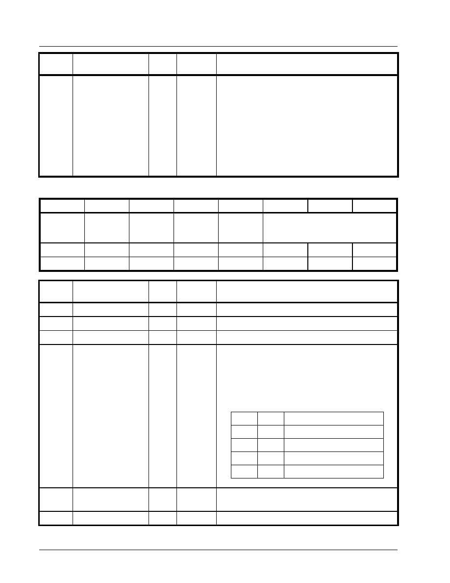
XRT79L71
PRELIMINARY
·Á
·Á
·Á
·Á
REV. P1.0.3
1 - CHANNEL DS3/E3 ATM UNI/PPP COMBO IC
108
0
Receive Equalizer
Enable
R/W
0
Receive Equalizer Enable - XRT79L71:
This READ/WRITE register bit permits the user to either
enable or disable the Receive Equalizer block within the
Receive Section of XRT79L71, as listed below.
0 - Disables the Receive Equalizer within the corresponding
channel.
1 - Enables the Receive Equalizer within the corresponding
channel.
N
OTE
: For virtually all applications, we recommend that the
user set this bit-field to "1" and enable the Receive
Equalizer.
LIU CHANNEL CONTROL REGISTER (ADDRESS = 0X1306)
B
IT
7
B
IT
6
B
IT
5
B
IT
4
B
IT
3
B
IT
2
B
IT
1
B
IT
0
Unused
SFM
Clock Out
Enable
SFM
Enable
RLB
LLB
Unused
R/O
R/O
R/O
R/W
R/W
R/O
R/O
R/O
0
0
0
0
0
0
0
0
B
IT
N
UMBER
N
AME
T
YPE
D
EFAULT
V
ALUE
D
ESCRIPTION
7 Unused
R/O
0
6
SFM Clock Out Enable
R/W
0
5
SFM Enable
R/W
0
4
RLB
R/W
0
Loop-Back Select - RLB Bit:
This READ/WRITE bit-field along with the corresponding
LLB bit-field permits the user to configure the XRT79L71
device into various loop-back modes.
The relationship between the settings for this input pin, the
corresponding LLB bit-field and the resulting Loop-back
Mode is presented below.
3
LLB
R/W
0
Loop-Back Select - LLB Bit-field:
Please see the description (above) for RLB.
2 - 0
Unused
R/O
0
B
IT
N
UMBER
N
AME
T
YPE
D
EFAULT
V
ALUE
D
ESCRIPTION
L L B
1
1
0
1
1
0
0
0
D igital Lo cal Loop-back M o de
A nalog L ocal Loop-back M ode
R em ote L oop-back M ode
N orm al (N o Loop-back) M o de
L o o p -b a c k M o d e
R L B

·Á
·Á
·Á
·Á
PRELIMINARY
XRT79L71
1 - CHANNEL DS3/E3 ATM UNI/PPP COMBO IC
REV. P1.0.3
109
JITTER ATTENUATOR CONTROL REGISTER (ADDRESS = 0X1307)
B
IT
7
B
IT
6
B
IT
5
B
IT
4
B
IT
3
B
IT
2
B
IT
1
B
IT
0
Unused
JA RESET
JA1
JA in Tx Path
JA0
R/O
R/O
R/O
R/W
R/W
R/W
R/W
R/W
0
0
0
0
0
0
0
0
B
IT
N
UMBER
N
AME
T
YPE
D
EFAULT
V
ALUE
D
ESCRIPTION
7 - 4
Unused
R/O
0
3
JA RESET
R/W
0
Jitter Attenuator RESET:
Writing a "0 to 1" transition within this bit-field will configure
the Jitter Attenuator (within the XRT79L71 device) to exe-
cute a RESET operation.
Whenever the user executes a RESET operation, then all of
the following will occur.
∑
The "READ" and "WRITE" pointers (within the Jitter
Attenuator FIFO) will be reset to their default values.
∑
The contents of the Jitter Attenuator FIFO will be flushed.
N
OTE
: The user must follow up any "0 to 1" transition with
the appropriate write operate to set this bit-field
back to "0", in order to resume normal operation
with the Jitter Attenuator.
2
JA1 Ch
R/W
0
Jitter Attenuator Configuration Select Input - Bit 1:
This READ/WRITE bit-field, along with Bit 0 (JA0) permits
the user to do any of the following.
∑
To enable or disable the Jitter Attenuator corresponding
to XRT79L71.
∑
To select the FIFO Depth for the Jitter Attenuator within
the XRT79L71 device.
The relationship between the settings of these two bit-fields
and the Enable/Disable States, and FIFO Depths is pre-
sented below.
J A 0
1
1
0
1
1
0
0
0
D isabled
D isabled
F IF O D epth = 32 bits
F IF O D epth = 16 bits
J itte r A tte n u a to r M o d e
J A 1

XRT79L71
PRELIMINARY
·Á
·Á
·Á
·Á
REV. P1.0.3
1 - CHANNEL DS3/E3 ATM UNI/PPP COMBO IC
110
1
JA in Tx Path Ch
R/W
0
Jitter Attenuator in Transmit/Receive Path Select Bit:
This input pin permits the user to configure the Jitter Attenu-
ator (within the XRT79L71 device) to operate in either the
Transmit or Receive path, as described below.
0 - Configures the Jitter Attenuator (within the XRT79L71
device) to operate in the Receive Path.
1 - Configures the Jitter Attenuator (within the XRT79L71
device) to operate in the Transmit Path.
0 JA0
Ch
R/W
0
Jitter Attenuator Configuration Select Input - Bit 0:
Please see the description for Bit 2 (JA1) within this Regis-
ter.
LIU RECEIVE APS/REDUNDANCY CONTROL REGISTER (ADDRESS = 0X1308)
B
IT
7
B
IT
6
B
IT
5
B
IT
4
B
IT
3
B
IT
2
B
IT
1
B
IT
0
Unused
RxON
R/O
R/O
R/O
R/O
R/O
R/O
R/O
R/W
0
0
0
0
0
0
0
0
B
IT
N
UMBER
N
AME
T
YPE
D
EFAULT
V
ALUE
D
ESCRIPTION
7 - 1
Reserved
R/O
0
0
RxON
R/W
0
Receiver Section ON - XRT79L71:
This READ/WRITE bit-field permits the user to either turn
on or turn off the Receive Section of XRT79L71. If the user
turns on the Receive Section, then XRT79L71 will begin to
receive the incoming DS3 or E3 data-stream via the RTIP
and RRING input pins.
Conversely, if the user turns off the Receive Section, then
the entire Receive Section (e.g., AGC and Receive Equal-
izer Block, Clock Recovery PLL, etc) will be powered down.
0 - Shuts off the Receive Section of XRT79L71.
1 - Turns on the Receive Section of XRT79L71.
B
IT
N
UMBER
N
AME
T
YPE
D
EFAULT
V
ALUE
D
ESCRIPTION

·Á
·Á
·Á
·Á
PRELIMINARY
XRT79L71
1 - CHANNEL DS3/E3 ATM UNI/PPP COMBO IC
REV. P1.0.3
111
DS3/E3 FRAMER BLOCK REGISTERS
The register map for the DS3/E3 Framer Block is presented in the Table below. Additionally, a detailed
description of each of the "DS3/E3 Framer" block registers is presented below.
OPERATING MODE REGISTER (DIRECT ADDRESS = 0X1100)
B
IT
7
B
IT
6
B
IT
5
B
IT
4
B
IT
3
B
IT
2
B
IT
1
B
IT
0
Local Loop
Back
IsDS3
Internal LOS
Enable
RESET
Interrupt
Enable
RESET
Frame Format
TimRefSel[1:0]
R/W
R/W
R/W
R/W
R/W
R/W
R/W
R/W
0
0
1
0
1
0
1
1
B
IT
N
UMBER
N
AME
T
YPE
D
ESCRIPTION
7
Local Loop Back
R/W
Framer Block Local Loop-back Mode:
This READ/WRITE bit field configures the Frame Generator/
Frame Synchronizer blocks to operate in the Local Loop-back
Mode. If the Frame Generator/Frame Synchronizer blocks are
configured to operate in the Local Loop-back Mode, then the
TxPOS, TxNEG and TxLineClk signal is internally looped back
into the RxPOS, RxNEG and RxLineClk signals.
0 - Normal Operating Mode
1 - Local Loop-back Mode
6
IsDS3
R/W
Is DS3 Mode:
This READ/WRITE bit-field, along with Bit 2 (Frame Format),
permits the user to configure the Frame Generator/Frame Syn-
chronizer block to operate in the appropriate framing format.
The relationship between the state of this bit-field, Bit 2 and the
resulting framing format is presented below.
5
Internal LOS Enable
R/W
Internal LOS Enable:
This READ/WRITE bit-field permits the user to enable or disable
the "Internal LOS Detector", within the Frame Synchronizer
block.
0 - Internal LOS Detector is disabled.
1 - Internal LOS Detector is enabled.
N
OTE
: The Internal LOS Detector only functions if the Channel
is configured to operate in the Dual-Rail Mode. If the
Channel is configured to operate in the Single-Rail
Mode, then the Internal LOS Detector will be disabled.
B it 6 (Is D S 3 )
1
0
1
1
1
0
0
0
D S 3, M 13
D S3, C -bit Parity
E3, ITU -T G .832
E3, ITU -T G .751
F ra m in g F o rm a t
B it 2 (F ra m e
F o rm a t)

XRT79L71
PRELIMINARY
·Á
·Á
·Á
·Á
REV. P1.0.3
1 - CHANNEL DS3/E3 ATM UNI/PPP COMBO IC
112
4
RESET
R/W
Software RESET Input:
A "0" to "1" transition in this bit-field commands a Software
RESET to the Channel. Once the user executes a Software
reset to the frame, all of the internal state machines will be reset;
and the Frame Synchronizer block will execute a "Reframe"
operation.
N
OTE
: For a Software Reset, the contents of the Command
Register will not be reset to their default values.
3
Interrupt Enable RESET
R/W
Interrupt Enable Reset:
This READ/WRITE bit-field permits the user to configure the
Channel to automatically disable any interrupt following its acti-
vation.
0 - Interrupts are NOT automatically disabled following their acti-
vation.
1 - Interrupt are automatically disabled following their activation.
2
Frame Format
R/W
Frame Format:
This READ/WRITE bit-field, along with Bit 6 (IsDS3), permits the
user to configure the Frame Generator/Frame Synchronizer
block to operate in the appropriate framing format. The relation-
ship between the state of this bit-field, Bit 2 and the resulting
framing format is presented below.
1 - 0
TimRefSel[1:0]
R/W
Time Reference Select:
These two READ/WRITE bit-fields permit the user to define both
the timing source and the framing-alignment source for the
Frame Generator block, as presented below.
B
IT
N
UMBER
N
AME
T
YPE
D
ESCRIPTION
B it 6 (Is D S 3 )
1
0
1
1
1
0
0
0
D S 3, M 13
D S3, C -bit Parity
E3, ITU -T G .832
E3, ITU -T G .751
F ra m in g F o rm a t
B it 2 (F ra m e
F o rm a t)
T im R e fS e l[1 :0 ]
11
10
01
00
T ransm it C lock Source for
th e F ram e G enerator block
T ransm it C lock Source for
th e F ram e G enerator block
T ransm it C lock Source for
th e F ram e G enerator block
Loop-T im ing (T im ing is
ta ken from the F ra m e
S ynchronizer block)
T im in g R e fe re n c e
A synchronous
A synchronous
T xD S3F P Inp ut
A synchronous
F ra m in g
R e fe re nc e

·Á
·Á
·Á
·Á
PRELIMINARY
XRT79L71
1 - CHANNEL DS3/E3 ATM UNI/PPP COMBO IC
REV. P1.0.3
113
I/O CONTROL REGISTER (DIRECT ADDRESS = 0X1101)
B
IT
7
B
IT
6
B
IT
5
B
IT
4
B
IT
3
B
IT
2
B
IT
1
B
IT
0
Disable
TxLOC
LOC
Disable
RxLOC
AMI/Zero
Sup*
Single-Rail/
Dual-Rail
DS3/E3 CLK
OUTInvert
DS3/E3 CLK
INInvert
Reframe
R/W
R/O
R/W
R/W
R/O
R/W
R/W
R/W
1
0
1
0
1
0
0
0
B
IT
N
UMBER
N
AME
T
YPE
D
ESCRIPTION
7
Disable TxLOC
R/W
Disable Transmit Loss of Clock Feature:
This READ/WRITE bit-field permits the user to either enable or
disable the "Transmit Loss of Clock" feature.
If this feature is enabled, then the DS3/E3 Framer block will
enable some circuitry that will terminate the current READ or
WRITE access (to the Microprocessor Interface), if a "Loss of
Transmit (or Frame Generator) Clock Event were to occur.The
intent behind this feature is to prevent any READ/WRITE
accesses (to the DS3/E3 Framer block) from "hanging" in the
event of a "Loss of Clock" event.
0 - Enables the "Transmit Loss of Clock" feature.
1 - Disables the "Transmit Loss of Clock" feature.
6
LOC
R/O
Loss of Clock Indicator:
This READ-ONLY bit-field indicates that the Channel has experi-
ences a Loss of Clock event.
5
Disable RxLOC
R/W
Disable Receive Loss of Clock Feature:
This READ/WRITE bit-field permits the user to either enable or
disable the "Receive Loss of Clock" feature.
If this feature is enabled, then the DS3/E3 Framer block will
enable some circuitry that will terminate the current READ or
WRITE access (to the Microprocessor Interface), if a "Loss of
Receiver (or Frame Synchronizer) Clock Event were to occur.
The intent behind this feature is to prevent any READ/WRITE
accesses (to the DS3/E3 Framer block) from "hanging" in the
event of a "Loss of Clock" event.
0 - Enables the "Receive Loss of Clock" feature.
1 - Disables the "Receive Loss of Clock" feature.
4
Reserved
3
Reserved

XRT79L71
PRELIMINARY
·Á
·Á
·Á
·Á
REV. P1.0.3
1 - CHANNEL DS3/E3 ATM UNI/PPP COMBO IC
114
2
DS3/E3 CLK_OUT Invert
R/W
DS3/E3_CLK_OUT Invert:
This READ/WRITE bit-field permits the user to configure the
DS3/E3 Frame Generator block within the XRT79L71, to update
the DS3/E3_DATA_OUT output pin upon either the rising or fall-
ing edge of DS3/E3_CLK_OUT.
0 - DS3/E3_DATA_OUT is updated upon the rising edge of DS3/
E3_Clk_OUT. The user should insure that the LIU IC will sample
"DS3/E3_DATA_OUT" upon the falling edge of "DS3/
E3_CLK_OUT".
1 - DS3/E3_DATA_OUT is updated upon the falling edge of DS3/
E3_CLK_OUT. The user should insure that the LIU IC will sam-
ple "DS3/E3_DATA_OUT" upon the rising edge of "DS3/
E3_CLK_OUT".NOTE: This bit-field is only active if the DS3/E3
Frame Generator block has been configured to operate in the
Egress Path.
1
DS3/E3 CLK_IN Invert
R/W
DS3/E3_CLK_IN Invert:
This READ/WRITE bit-field permits the user to configure the
XRT79L71, to sample and latch the "DS3/E3_DATA_IN" input pin
upon either the rising or falling edge of DS3/E3_CLK_IN.
0 - DS3/E3_DATA_IN is sampled upon the falling edge of DS3/
E3_CLK_IN.
1 - DS3/E3_DATA is sampled upon the rising edge of DS3/
E3_CLK_IN.NOTE: This bit-field is only active if the Primary
Frame Synchronizer block has been configured to operate in the
Ingress Path.
0
Reframe
R/W
DS3/E3 Frame Synchronizer Block - Reframe Command:
A "0" to "1" transition, within this bit-field commands the DS3/E3
Frame Synchronizer block to exit the Frame Maintenance Mode,
and go back and enter the Frame Acquisition Mode.
N
OTE
: The user should go back and set this bit-field to "0"
following execution of the "Reframe" Command.
B
IT
N
UMBER
N
AME
T
YPE
D
ESCRIPTION

·Á
·Á
·Á
·Á
PRELIMINARY
XRT79L71
1 - CHANNEL DS3/E3 ATM UNI/PPP COMBO IC
REV. P1.0.3
115
BLOCK INTERRUPT ENABLE REGISTER (DIRECT ADDRESS = 0X1104)
B
IT
7
B
IT
6
B
IT
5
B
IT
4
B
IT
3
B
IT
2
B
IT
1
B
IT
0
DS3/E3
Frame Synch
Block
Interrupt
Enable
Unused
DS3/E3Frame
Generator-
Block
Interrupt
Enable
One Second
Interrupt
R/W
R/O
R/O
R/O
R/O
R/O
R/W
R/W
0
0
0
0
0
0
0
0
B
IT
N
UMBER
N
AME
T
YPE
D
ESCRIPTION
7
DS3/E3 Frame Synch
Block Interrupt Enable
R/W
DS3/E3 Frame Synchronizer Block Interrupt Enable:
This READ/WRITE bit-field permits the user to enable or disable
the Frame Synchronizer block for Interrupt Generation. If the
user enables the Frame Synchronizer block (for Interrupt Gener-
ation) at the block level, the user still needs to enable the inter-
rupts at the "Source" level, as well; in order for these interrupts to
be enabled.
However, if the user disables the Frame Synchronizer block (for
Interrupt Generation) at the Block Level, then ALL Frame Syn-
chronizer-related blocks are disabled.
0 - Frame Synchronizer block is Disabled for Interrupt Genera-
tion.
1 - Frame Synchronizer block is enabled (at the Block level) for
Interrupt Generation.
6 - 2
Unused
R/O
1
DS3/
E3FrameGeneratorBlockI
nterrupt Enable
R/W
DS3/E3 Frame Generator Block Interrupt Enable:
This READ/WRITE bit-field permits the user to enable or disable
the Frame Generator block for Interrupt Generation. If the user
enables the Frame Generator block (for Interrupt Generation) at
the block level, the user still needs to enable the interrupts at the
"Source" level, as well; in order for these interrupts to be
enabled.
However, if the user disables the Frame Generator block (for
Interrupt Generation) at the Block Level, then ALL Frame Gener-
ator-related blocks are disabled.
0 - Frame Generator block is Disabled for Interrupt Generation.
1 - Frame Generator block is Enabled (at the Block Level) for
Interrupt Generation.
0
One Second Interrupt
R/W
One Second Interrupt Enable:
This READ/WRITE bit-field permits the user to enable or disable
the One-Second Interrupt. If the user enables this interrupt, then
the XRT79L71 will generate an interrupt at one second intervals.
0 - One Second Interrupt is disabled.
1 - One Second Interrupt is enabled.

XRT79L71
PRELIMINARY
·Á
·Á
·Á
·Á
REV. P1.0.3
1 - CHANNEL DS3/E3 ATM UNI/PPP COMBO IC
116
BLOCK INTERRUPT STATUS REGISTER (DIRECT ADDRESS = 0X1105)
B
IT
7
B
IT
6
B
IT
5
B
IT
4
B
IT
3
B
IT
2
B
IT
1
B
IT
0
DS3/E3
Frame
Sync Block
Interrupt
Status
Unused
DS3/E3
Frame
Generator
Block
Interrupt
Status
One Second
Interrupt
R/O
R/O
R/O
R/O
R/O
R/O
R/O
RUR
0
0
0
0
0
0
0
0
B
IT
N
UMBER
N
AME
T
YPE
D
ESCRIPTION
7
DS3/E3 Frame Synch
Block Interrupt Status
R/O
DS3/E3 Frame Synchronizer Block Interrupt Status:
This READ-ONLY bit-field indicates whether or not a "DS3/E3
Frame Synchronizer Block"-related interrupt is requesting inter-
rupt service.
0 - The DS3/E3 Frame Synchronizer block is NOT requesting
any interrupt service.
1 - The DS3/E3 Frame Synchronizer block is requesting interrupt
service.
6 - 2
Unused
R/O
1
DS3/E3 Frame Generator
Block Interrupt Status
R/O
DS3/E3 Frame Generator Block Interrupt Status:
This READ-ONLY bit-field indicates whether or not a "DS3/E3
Frame Generator" -related interrupt is requesting interrupt ser-
vice.
0 - The DS3/E3 Frame Generator block is NOT requesting any
interrupt service.
1 - The DS3/E3 Frame Synchronizer block is requesting interrupt
service.
0
One Second Interrupt
Status
RUR
One Second Interrupt Status:
This RESET-upon-READ bit-field indicates whether or not a
"One Second" Interrupt has occurred since the last read of this
register.
0 - The One Second Interrupt has NOT occurred since the last
read of this register.
1 - The One Second Interrupt has occurred since the last read of
this register.

·Á
·Á
·Á
·Á
PRELIMINARY
XRT79L71
1 - CHANNEL DS3/E3 ATM UNI/PPP COMBO IC
REV. P1.0.3
117
TEST REGISTER (DIRECT ADDRESS = 0X110C)
B
IT
7
B
IT
6
B
IT
5
B
IT
4
B
IT
3
B
IT
2
B
IT
1
B
IT
0
TxOHSrc
Unused
RxPRBS
Lock
RxPRBS
Enable
TxPRBS
Enable
Unused
R/W
R/O
R/O
R/O
R/W
R/W
R/O
R/O
0
0
0
0
0
0
0
0
B
IT
N
UMBER
N
AME
T
YPE
D
ESCRIPTION
7
TxOHSrc
R/W
Transmit Overhead Bit Source:
This READ/WRITE bit-field permits the user to configure the
Frame Generator to accept and insert overhead bits/bytes which
are input via the "Payload Data Input Interface" block, as indi-
cated below.
0 - Overhead bits/bytes are internally generated by the Frame
Generator block.
1 - Overhead bits/byte data is accepted from the Payload Data
Input Interface block.NOTE: This register bit applies to all fram-
ing formats that are supported by the Frame Generator block.
6 - 5
Unused
R/O
4
RxPRBS Lock
R/O
PRBS Lock Indicator:
This READ-ONLY bit-field indicates whether or not the PRBS
Receiver (within the Channel) has acquired "PRBS Lock" with
the payload data of the incoming DS3 or E3 data stream.
0 - PRBS Receiver does not have PRBS Lock with the incoming
data stream.
1 - PRBS Receiver does have PRBS Lock with the incoming
data stream.
N
OTE
: This bit-field is not valid if the PRBS Receiver is disabled,
or if the Frame Synchronizer block is bypassed.
3
RxPRBS Enable
R/W
Receive PRBS Enable:
This READ/WRITE bit-field permits the user to either enable or
disable the PRBS Receiver within the Frame Synchronizer block.
Once the user enables the PRBS Receiver, then it will proceed
to attempt to acquire and maintain pattern (or PRBS Lock) within
the payload bits, within the incoming DS3 or E3 data stream.
0 - Disables the PRBS Receiver.
1 - Enables the PRBS Receiver.
N
OTE
: This bit-field is ignored if the Frame Synchronizer block is
by-passed.

XRT79L71
PRELIMINARY
·Á
·Á
·Á
·Á
REV. P1.0.3
1 - CHANNEL DS3/E3 ATM UNI/PPP COMBO IC
118
2
TxPRBS Enable
R/W
Transmit PRBS Enable:
This READ/WRITE bit-field permits the user to either enable or
disable the PRBS Generator within the Frame Generator block.
Once the user enables the PRBS Generator block, then it will
proceed to insert a PRBS pattern into the payload bits, within the
outbound DS3 or E3 data stream.
0 - Disables the PRBS Generator.
1 - Enables the PRBS Generator.
N
OTE
: This bit-field is ignored if the Frame Generator block is
by-passed.
1 - 0
Unused
R/O
B
IT
N
UMBER
N
AME
T
YPE
D
ESCRIPTION

·Á
·Á
·Á
·Á
PRELIMINARY
XRT79L71
1 - CHANNEL DS3/E3 ATM UNI/PPP COMBO IC
REV. P1.0.3
119
RECEIVE DS3 RELATED REGISTERS
RXDS3 CONFIGURATION AND STATUS REGISTER (DIRECT ADDRESS = 0X1110)
B
IT
7
B
IT
6
B
IT
5
B
IT
4
B
IT
3
B
IT
2
B
IT
1
B
IT
0
RxAIS
RxLOS
RxIdle
RxOOF
Unused
Framing with
Valid P-Bits
F-SyncAlgo
M-SyncAlgo
R/O
R/O
R/O
R/O
R/O
R/W
R/W
R/W
0
0
0
1
0
1
0
0
B
IT
N
UMBER
N
AME
T
YPE
D
ESCRIPTION
7
RxAIS
R/O
Receive AIS Defect Indicator:
This READ-ONLY bit-field indicates whether or not the Frame
Synchronizer block is currently detecting the AIS pattern in its
incoming path.
0 - Frame Synchronizer block is NOT currently detecting an AIS
pattern in its incoming path.
1 - Frame Synchronizer block is currently detecting an AIS pat-
tern in its incoming path.
6
RxLOS
R/O
Receive LOS Defect Indicator:
This READ-ONLY bit-field indicates whether or not the Frame
Synchronizer block is currently detecting the LOS condition, in its
incoming path.
0 - Frame Synchronizer block is NOT currently declaring an LOS
condition in its incoming path.
1 - Frame Synchronizer block is currently detecting an LOS con-
dition in its incoming path.
5
RxIdle
R/O
Receive Idle Signal Indicator:
This READ-ONLY bit-field indicates whether or not the Frame
Synchronizer block is currently detecting the DS3 Idle pattern, in
its incoming path.
0 - Frame Synchronizer block is NOT currently detecting the DS3
Idle Pattern, in its incoming path.
1 - Frame Synchronizer block is currently detecting the DS3 Idle
Pattern in its incoming path.
4
RxOOF
R/O
Receive OOF Defect Indicator:
This READ-ONLY bit-field indicates whether or not the Frame
Synchronizer block is currently declaring an OOF (Out of Frame)
condition.
0 - Frame Synchronizer block is NOT currently declaring the
OOF condition.
1 - Frame Synchronizer block is currently declaring the OOF
condition.
3
Unused
R/O

XRT79L71
PRELIMINARY
·Á
·Á
·Á
·Á
REV. P1.0.3
1 - CHANNEL DS3/E3 ATM UNI/PPP COMBO IC
120
2
Framing with Valid P Bits
R/W
Framing with Valid P-Bit Select:
This READ/WRITE bit-field permits the user to choose between
two different sets of DS3 Frame Acquisition/Maintenance crite-
ria.
0 - Normal Framing Acquisition/Maintenance Criteria (without P-
bit Checking)In this mode, the Frame Synchronizer block will
declare the "In-frame" state, one it has successfully completed
both the "F-Bit Search" and the "M-Bit Search" states.
1 - Framing Acquisition/Maintenance with P-bit CheckingIn this
mode, the Frame Synchronizer block will (in addition to passing
through the "F-Bit Search" and "M-Bit Search" states) also verify
valid P-bits, prior to declaring the "In-Frame" state.
N
OTE
: This bit-field is ignored if the Frame Synchronizer block is
by-passed.
1
F-Sync Algo
R/W
F-Bit Search State Criteria Select:
This READ/WRITE bit-field permits the user to choose between
two different sets of DS3 Out of Frame (OOF) Declaration crite-
ria.
0 - OOF is declared when 6 out of 15 F-bits are erred.
1 - OOF is declared when 3 out of 15 F-bits are erred.NOTE:
This bit-field is ignored if the Frame Synchronizer block is by-
passed.
0
M-Sync Algo
R/W
M-Bit Search State Criteria Select:
This READ/WRITE bit-field permits the user to choose between
two different sets of DS3 Out of Frame (OOF) Declaration crite-
ria.
0 - M-bit Errors do not result in the Frame Synchronizer declaring
OOF.
1 - OOF is declared when all M-bits, within 3 out of 4 DS3 frames
are in error.
B
IT
N
UMBER
N
AME
T
YPE
D
ESCRIPTION

·Á
·Á
·Á
·Á
PRELIMINARY
XRT79L71
1 - CHANNEL DS3/E3 ATM UNI/PPP COMBO IC
REV. P1.0.3
121
RXDS3 STATUS REGISTER (DIRECT ADDRESS = 0X1111)
B
IT
7
B
IT
6
B
IT
5
B
IT
4
B
IT
3
B
IT
2
B
IT
1
B
IT
0
Unused
RxFERF
RxAIC
RxFEBE[2:0]
R/O
R/O
R/O
R/O
R/O
R/O
R/O
R/O
0
0
0
0
0
0
0
0
B
IT
N
UMBER
N
AME
T
YPE
D
ESCRIPTION
7 - 5
Unused
R/O
4
RxFERF
R/O
Receive FERF (Far-End Receive Failure) Defect Indicator:
This READ-ONLY bit-field indicates whether or not the Frame
Synchronizer block is currently declaring a FERF condition.
0 - The Frame Synchronizer block is NOT currently declaring the
FERF condition.
1 - The Frame Synchronizer block is currently declaring the
FERF condition.
N
OTE
: This bit-field is not valid if the Frame Synchronizer block
has been by-passed.
3
RxAIC
R/O
Receive AIC State:
This READ-ONLY bit-field indicates the current state of the AIC
bit-field within the incoming DS3 data-stream.
0 - Indicates that the Frame Synchronizer block has received at
least 2 consecutive M-frames that have the AIC bit-field set to
"0".
1 - Indicates that the Frame Synchronizer block has received at
least 63 consecutive M-frames that have the AIC bit-field set to
"1".
2 - 0
RxFEBE[2:0]
R/O
Receive FEBE (Far-End Block Error) Value:
These READ-ONLY bit-fields reflect the FEBE value within the
most recently received DS3 frame. RxFEBE[2:0] = [1, 1, 1] indi-
cates a normal condition. All other values for RxFEBE[2:0] indi-
cates an erred condition at the remote terminal equipment.
N
OTES
:
1.
1.This bit-field is not valid if the Frame Synchronizer
block has been by-passed.
2.
This bit-field is not valid if the Frame Synchronizer block
has been configured to operate in the M13 Framing
format.

XRT79L71
PRELIMINARY
·Á
·Á
·Á
·Á
REV. P1.0.3
1 - CHANNEL DS3/E3 ATM UNI/PPP COMBO IC
122
RXDS3 INTERRUPT ENABLE REGISTER (DIRECT ADDRESS = 0X1112)
B
IT
7
B
IT
6
B
IT
5
B
IT
4
B
IT
3
B
IT
2
B
IT
1
B
IT
0
Detection of
CP Bit Error
Interrupt
Enable
Change of
LOS
Condition
Interrupt
Enable
Change of
AIS
Condition
Interrupt
Enable
Change of
Idle
Condition
Interrupt
Enable
Change of
FERF
Condition
Interrupt
Enable
Change of
AIC State
Interrupt
Enable
Change of
OOF
Condition
Interrupt
Enable
Detection of
P-Bit Error
Interrupt
Enable
R/W
R/W
R/W
R/W
R/W
R/W
R/W
R/W
0
0
0
0
0
0
0
0
B
IT
N
UMBER
N
AME
T
YPE
D
ESCRIPTION
7
Detection of CP Bit Error
Interrupt Enable
R/W
Detection of CP-Bit Error Interrupt Enable:
This READ/WRITE bit-field permits the user to either enable or
disable the "Detection of CP-Bit Error" Interrupt, within the Chan-
nel. If the user enables this interrupt, then the Frame Synchro-
nizer block will generate an interrupt anytime it detects CP bit
errors.
0 - Disables the "Detection of CP Bit Error" Interrupt.
1 - Enables the "Detection of CP-Bit Error" Interrupt.
N
OTE
: This bit-field is ignored if the Frame Synchronizer block is
by-passed.
6
Change of LOS Condition
Interrupt Enable
R/W
Change in LOS Condition Interrupt Enable:
This READ/WRITE bit-field permits the user to either enable or
disable the "Change in LOS (Loss of Signal) Condition" Interrupt,
within the Channel. If the user enables this interrupt, then the
Frame Synchronizer block will generate an interrupt in response
to either of the following conditions.
∑
The instant that the channel declares an LOS condition.
∑
The instant that the channel clears the LOS condition.
0 - Disables the "Change in LOS Condition" Interrupt.
1 - Enables the "Change in LOS Condition" Interrupt.
5
Change of AIS Condition
Interrupt Enable
R/W
Change in AIS Condition Interrupt Enable:
This READ/WRITE bit-field permits the user to either enable or
disable the "Change in AIS (Alarm Indication Signal) Condition"
Interrupt, within the Channel. If the user enables this interrupt,
then the Frame Synchronizer block will generate an interrupt in
response to either of the following conditions.∑ The instant that
the channel declares an AIS condition.∑ The instant that the
channel clears the AIS condition.
0 - Disables the "Change in AIS Condition" Interrupt.
1 - Enables the "Change in AIS Condition" Interrupt.
N
OTE
: This bit-field is ignored if the Frame Synchronizer block is
by-passed.

·Á
·Á
·Á
·Á
PRELIMINARY
XRT79L71
1 - CHANNEL DS3/E3 ATM UNI/PPP COMBO IC
REV. P1.0.3
123
4
Change of Idle Condition
Interrupt Enable
R/W
Change in Idle Condition Interrupt Enable:
This READ/WRITE bit-field permits the user to either enable or
disable the "Change in Idle Condition" Interrupt, within the Chan-
nel. If the user enables this interrupt, then the Frame Synchro-
nizer block will generate an interrupt in response to either of the
following conditions.
∑
The instant that the channel detects the Idle condition.
∑
The instant that the channel ceases to detect the Idle
condition.
0 - Disables the "Change in Idle Condition" Interrupt.
1 - Enables the "Change in Idle Condition" Interrupt.
N
OTE
: This bit-field is ignored if the Frame Synchronizer block is
by-passed.
3
Change of FERF
Condition Interrupt
Enable
R/W
Change in FERF Condition Interrupt Enable:
This READ/WRITE bit-field permits the user to either enable or
disable the "Change in FERF (Far-End Receive Failure) Condi-
tion" Interrupt, within the Channel. If the user enables this inter-
rupt, then the Frame Synchronizer block will generate an
interrupt in response to either of the following conditions.
∑
The instant that the channel declares an FERF condition.
∑
The instant that the channel clears the FERF condition.
0 - Disables the "Change in FERF Condition" Interrupt.
1 - Enables the "Change in FERF Condition" Interrupt.
N
OTE
: This bit-field is ignored if the Frame Synchronizer block is
by-passed.
2
Change of AIC State
Interrupt Enable
R/W
Change in AIC State Interrupt Enable:
This READ/WRITE bit-field permits the user to either enable or
disable the "Change in AIC State" Interrupt, within the Channel.
If the user enables this interrupt, then the Frame Synchronizer
block will generate an interrupt in response to it detecting a
change in the AIC bit-field, within the incoming DS3 data stream.
N
OTE
: This bit-field is ignored if the Frame Synchronizer block is
by-passed.
1
Change of OOF
Condition Interrupt
Enable
R/W
Change in OOF Condition Interrupt Enable:
This READ/WRITE bit-field permits the user to either enable or
disable the "Change in OOF (Out of Frame) Condition" Interrupt,
within the Channel. If the user enables this interrupt, then the
Frame Synchronizer block will generate an interrupt in response
to either of the following conditions.
∑
The instant that the channel declares an OOF condition.
∑
The instant that the channel clears the OOF condition.
0 - Disables the "Change in OOF Condition" Interrupt.
1 - Enables the "Change in OOF Condition" Interrupt.
N
OTE
: This bit-field is ignored if the Frame Synchronizer block is
by-passed.
B
IT
N
UMBER
N
AME
T
YPE
D
ESCRIPTION

XRT79L71
PRELIMINARY
·Á
·Á
·Á
·Á
REV. P1.0.3
1 - CHANNEL DS3/E3 ATM UNI/PPP COMBO IC
124
0
Detection of P-Bit Error
Interrupt Enable
R/W
Detection of P-Bit Error Interrupt Enable:
This READ/WRITE bit-field permits the user to either enable or
disable the "Detection of CP-Bit Error" Interrupt, within the Chan-
nel. If the user enables this interrupt, then the Frame Synchro-
nizer block will generate an interrupt anytime it detects CP bit
errors.
0 - Disables the "Detection of CP Bit Error" Interrupt.
1 - Enables the "Detection of CP-Bit Error" Interrupt.
N
OTE
: This bit-field is ignored if the Frame Synchronizer block is
by-passed.
B
IT
N
UMBER
N
AME
T
YPE
D
ESCRIPTION

·Á
·Á
·Á
·Á
PRELIMINARY
XRT79L71
1 - CHANNEL DS3/E3 ATM UNI/PPP COMBO IC
REV. P1.0.3
125
RXDS3 INTERRUPT STATUS REGISTER (DIRECT ADDRESS = 0X1113)
B
IT
7
B
IT
6
B
IT
5
B
IT
4
B
IT
3
B
IT
2
B
IT
1
B
IT
0
Detection of
CP Bit Error
Interrupt
Status
Change of
LOS
Condition
Interrupt
Status
Change of
AIS
Condition
Interrupt
Status
Change of
Idle
Condition
Interrupt
Status
Change of
FERF
Condition
Interrupt
Status
Change of
AIC State
Interrupt
Status
Change of
OOF
Condition
Interrupt
Status
Detection of
P-Bit Error
Interrupt
Status
RUR
RUR
RUR
RUR
RUR
RUR
RUR
RUR
0
0
0
0
0
0
0
0
B
IT
N
UMBER
N
AME
T
YPE
D
ESCRIPTION
7
Detection of CP Bit Error
Interrupt Status
RUR
Detection of CP-Bit Error Interrupt Status:
This RESET-upon-READ bit-field indicates whether or not the
"Detection of CP-Bit Error" Interrupt has occurred since the last
read of this register.
0 - The "Detection of CP-Bit Error" Interrupt has not occurred
since the last read of this register.
1 - The "Detection of CP-Bit Error" Interrupt has occurred since
the last read of this register.
N
OTE
: This bit-field is ignored if the Frame Synchronizer block is
by-passed.
6
Change of LOS Condition
Interrupt Status
RUR
Change in LOS Condition Interrupt Status:
This RESET-upon-READ register indicates whether or not the
"Change in LOS Condition" Interrupt has occurred since the last
read of this register.
0 - The "Change in LOS Condition" Interrupt has not occurred
since the last read of this register.
1 - The "Change in LOS Condition" Interrupt has occurred since
the last read of this register.
N
OTE
: This bit-field is ignored if the Frame Synchronizer block is
by-passed.
5
Change of AIS Condition
Interrupt Status
RUR
Change in AIS Condition Interrupt Status:
This RESET-upon-READ register indicates whether or not the
"Change in LOS Condition" Interrupt has occurred since the last
read of this register.
0 - The "Change in LOS Condition" Interrupt has not occurred
since the last read of this register.
1 - The "Change in LOS Condition" Interrupt has occurred since
the last read of this register.
N
OTE
: This bit-field is ignored if the Frame Synchronizer block is
by-passed.

XRT79L71
PRELIMINARY
·Á
·Á
·Á
·Á
REV. P1.0.3
1 - CHANNEL DS3/E3 ATM UNI/PPP COMBO IC
126
4
Change of Idle Condition
Interrupt Status
RUR
Change in Idle Condition Interrupt Status:
This RESET-upon-READ register indicates whether or not the
"Change in Idle Condition" interrupt has occurred since the last
read of this register.
0 - The "Change in Idle Condition" Interrupt has not occurred
since the last read of this register.
1 - The "Change in Idle Condition" Interrupt has occurred since
the last read of this register.
N
OTE
: This bit-field is ignored if the Frame Synchronizer block is
by-passed.
3
Change of FERF Condi-
tion Interrupt Status
RUR
Change in FERF Condition Interrupt Status:
This RESET-upon-READ register indicates whether or not the
"Change in FERF Condition" Interrupt has occurred since the
last read of this register.
0 - The "Change in FERF Condition" Interrupt has not occurred
since the last read of this register.
1 - The "Change in FERF Condition" Interrupt has occurred
since the last read of this register.
N
OTE
: This bit-field is ignored if the Frame Synchronizer block is
by-passed.
2
Change of AIC State
Interrupt Status
RUR
Change in AIC State Interrupt Status:
This RESET-upon-READ register bit indicates whether or not the
"Change in AIC State" interrupt has occurred since the last read
of this register.
0 - The "Change in AIC State" Interrupt has not occurred since
the last read of this register.
1 - The "Change in AIC State" Interrupt has occurred since the
last read of this register.
N
OTE
: This bit-field is ignored if the Frame Synchronizer block is
by-passed.
1
Change of OOF Condi-
tion Interrupt Status
RUR
Change in OOF Condition Interrupt Status:
This RESET-upon-READ register indicates whether or not the
"Change in OOF Condition" Interrupt has occurred since the last
read of this register.
0 - The "Change in OOF Condition" Interrupt has not occurred
since the last read of this register.
1 - The "Change in OOF Condition" Interrupt has occurred since
the last read of this register.
N
OTE
: This bit-field is ignored if the Frame Synchronizer block is
by-passed.
0
Detection of P-Bit Error
Interrupt Status
RUR
Detection of P-Bit Error Interrupt Status:
This RESET-upon-READ bit-field indicates whether or not the
"Detection of CP-Bit Error" Interrupt has occurred since the last
read of this register.
0 - The "Detection of CP-Bit Error" Interrupt has not occurred
since the last read of this register.
1 - The "Detection of CP-Bit Error" Interrupt has occurred since
the last read of this register.
N
OTE
: This bit-field is ignored if the Frame Synchronizer block is
by-passed.
B
IT
N
UMBER
N
AME
T
YPE
D
ESCRIPTION

·Á
·Á
·Á
·Á
PRELIMINARY
XRT79L71
1 - CHANNEL DS3/E3 ATM UNI/PPP COMBO IC
REV. P1.0.3
127
RXDS3 SYNC DETECT REGISTER (DIRECT ADDRESS = 0X1114)
B
IT
7
B
IT
6
B
IT
5
B
IT
4
B
IT
3
B
IT
2
B
IT
1
B
IT
0
Unused
P-Bit Correct
F Algorithm
One and Only
R/O
R/O
R/O
R/O
R/O
R/W
R/W
R/W
0
0
0
0
0
0
0
0
B
IT
N
UMBER
N
AME
T
YPE
D
ESCRIPTION
7 - 3
Unused
R/O
2
P-Bit Correct
R/W
P-Bit Correct:
This READ/WRITE bit-field permits the user to enable or disable
the "P-Bit Correct" feature within the DS3 Frame Synchronizer
block. If the user enables this feature, then the DS3 Frame Syn-
chronizer will automatically invert the state of any P-bits, when-
ever it detects "P-bit errors".
0 - Disables the "P-Bit Correct" feature.
1 - Enables the "P-Bit Correct" feature
1
F Algorithm
R/W
F-Bit Search Algorithm Select:
This READ/WRITE bit-field permits the user to select the "F-bit
acquisition" criteria, when the Frame Synchronizer block is oper-
ating in the "F-Bit Search" state.
0 - Frame Synchronizer will move on to the "M-Bit Search" state,
when it has properly located 10 consecutive F-bits.
1 - Frame Synchronizer will move on to the "M-Bit Search" state,
when it has properly located 16 consecutive F-bits.
0
One and Only
R/W
F-Bit Search/Mimic-Handling Algorithm Select:
This READ/WRITE bit-field permits the user to select the "F-bit
acquisition" criteria, when the Frame Synchronizer block is oper-
ating in the "F-Bit Search" state.
0 - Frame Synchronizer will move on to the "M-Bit Search" state,
when it has properly located 10 (or 16) consecutive F-bits (as
configured in Bit 1 of this register).
1 - Frame Synchronizer will move on to the "M-Bit Search" state,
when (1) it has properly located 10 (or 16) consecutive F-bits;
and (2) when it has located and identified only one viable "F-Bit
Alignment" candidate.
N
OTE
: If this bit is set to "1", then the Frame Synchronizer block
will NOT transition into the "M-Bit Search" state, as long
as at least two viable candidate set of bits appear to
function as the F-bits.

XRT79L71
PRELIMINARY
·Á
·Á
·Á
·Á
REV. P1.0.3
1 - CHANNEL DS3/E3 ATM UNI/PPP COMBO IC
128
RXDS3 FEAC REGISTER (DIRECT ADDRESS = 0X1116)
B
IT
7
B
IT
6
B
IT
5
B
IT
4
B
IT
3
B
IT
2
B
IT
1
B
IT
0
Unused
RxFEACCode[5:0]
Unused
R/O
R/O
R/O
R/O
R/O
R/O
R/O
R/O
0
1
1
1
1
1
1
0
B
IT
N
UMBER
N
AME
T
YPE
D
ESCRIPTION
7
Unused
R/O
6 - 1
RxFEAC_Code[5:0]
R/O
Receive FEAC Code Word:
These READ-ONLY bit-fields contain the value of the most
recently "validated" FEAC Code word.
0
Unused
R/O

·Á
·Á
·Á
·Á
PRELIMINARY
XRT79L71
1 - CHANNEL DS3/E3 ATM UNI/PPP COMBO IC
REV. P1.0.3
129
RXDS3 FEAC INTERRUPT ENABLE/STATUS REGISTER (DIRECT ADDRESS = 0X1117)
B
IT
7
B
IT
6
B
IT
5
B
IT
4
B
IT
3
B
IT
2
B
IT
1
B
IT
0
Unused
FEAC
Valid
RxFEAC
Remove
Interrupt
Enable
RxFEAC
Remove
Interrupt
Status
RxFEAC
Valid
Interrupt
Enable
RxFEAC
Valid
Interrupt
Status
R/O
R/O
R/O
R/O
R/W
RUR
R/W
RUR
0
0
0
0
0
0
0
0
B
IT
N
UMBER
N
AME
T
YPE
D
ESCRIPTION
7 - 5
Unused
R/O
Please set to "0" (the default value) for normal operation.
4
FEAC Valid
R/O
FEAC Message Validation Indicator:
This READ-ONLY bit-field indicates that the FEAC Code (which
resides within the "RxDS3 FEAC" Register) has been validated
by the Receive FEAC Controller. The Receive FEAC Controller
will validate a FEAC codeword if it has received this codeword in
8 out of the last 10 FEAC Messages. Polled systems can moni-
tor this bit-field, when checking for a newly validated FEAC code-
word.
0 - FEAC Message is not (or no longer) validated.
1 - FEAC Message has been validated.
3
RxFEAC Remove
Interrupt Enable
R/W
FEAC Message Remove Interrupt Enable:
This READ/WRITE bit-field permits the user to either enable or
disable the "Receive FEAC Remove Interrupt". If the user
enables this interrupt, then the Framer Synchronizer will gener-
ate an interrupt anytime the most recently validated FEAC Mes-
sage has been removed. The Receive FEAC Controller will
remove a validated FEAC codeword, if it has received a different
codeword in 3 out of the last 10 FEAC Messages.
0 - Receive FEAC Remove Interrupt is disabled.
1 - Receive FEAC Remove Interrupt is enabled.
N
OTE
: This bit-field is ignored if the Frame Synchronizer block is
by-passed.
2
RxFEAC Remove
Interrupt Status
RUR
FEAC Message Remove Interrupt Status:
This RESET-upon-READ bit-field indicates whether or not the
"FEAC Message Remove Interrupt" has occurred since the last
read of this register.
0 - FEAC Message Remove Interrupt has NOT occurred since
the last read of this register.
1 - FEAC Message Remove Interrupt has occurred since the last
read of this register.
1
RxFEAC Valid Interrupt
Enable
R/W
FEAC Message Validation Interrupt Enable:
This READ/WRITE bit-field permits the user to either enable or
disable the FEAC Message Validation Interrupt. If the user
enables this interrupt, then the Frame Synchronizer block will
generate an interrupt anytime a new FEAC Codeword has been
validated by the Receive FEAC Controller.
0 - FEAC Message Validation Interrupt is NOT enabled.
1 - FEAC Message Validation Interrupt is enabled.

XRT79L71
PRELIMINARY
·Á
·Á
·Á
·Á
REV. P1.0.3
1 - CHANNEL DS3/E3 ATM UNI/PPP COMBO IC
130
0
RxFEAC Valid Interrupt
Status
RUR
FEAC Message Validation Interrupt Status:
This RESET-upon-READ bit-field indicates whether or not the
"FEAC Message Validation" Interrupt has occurred since the last
read of this register.
0 - FEAC Message Validation Interrupt has not occurred since
the last read of this register.
1 - FEAC Message Validation Interrupt has occurred since the
last read of this register.
B
IT
N
UMBER
N
AME
T
YPE
D
ESCRIPTION

·Á
·Á
·Á
·Á
PRELIMINARY
XRT79L71
1 - CHANNEL DS3/E3 ATM UNI/PPP COMBO IC
REV. P1.0.3
131
RXDS3 LAPD CONTROL REGISTER (DIRECT ADDRESS = 0X1118)
B
IT
7
B
IT
6
B
IT
5
B
IT
4
B
IT
3
B
IT
2
B
IT
1
B
IT
0
RxLAPDAny
Unused
RxLAPD
Enable
RxLAPD
Interrupt
Enable
RxLAPD
Interrupt
Status
R/W
R/O
R/O
R/O
R/O
R/W
R/W
RUR
0
0
0
0
0
0
0
0
B
IT
N
UMBER
N
AME
T
YPE
D
ESCRIPTION
7
RxLAPD Any
R/W
Receive LAPD - Any kind:
This READ/WRITE bit-field permits the user to configure the
LAPD Receiver to receive any kind of LAPD Message (or HDLC
Message) with a size of 82 bytes or less. If the user implements
this option, then the LAPD Receiver will be capable of receiving
any kind of HDLC Message (with any value of header bytes).
The only restriction is that the size of the HDLC Message must
not exceed 82 bytes.
0 - Does not invoke this "Any Kind of HDLC Message" feature.
In this case, the LAPD Receiver will only receive HDLC Mes-
sages that contains the Bellcore GR-499-CORE values for SAPI
and TEI.
1- Invokes this "Any Kind of HDLC Message" feature. In this
case, the LAPD Receiver will be able to receive HDLC Mes-
sages that contain any header byte values.
N
OTES
:
1.
This bit-field is ignored if the Frame Synchronizer block
is by-passed.
2.
The user can determine the size (or byte-count) of the
most recently received LAPD/PMDL Message, by
reading the contents of the "RxLAPD Byte Count"
Register (Direct Address = 0xNE84)
6 - 3
Unused
R/O
2
RxLAPD Enable
R/W
LAPD Receiver Enable:
This READ/WRITE bit-field permits the user to either enable or
disable the LAPD Receiver within the channel. If the user
enables the LAPD Receiver, then it will immediately begin
extracting out and monitoring the data (being carried via the "DL"
bits) within the incoming DS3 data stream.
0 - Enables the LAPD Receiver.
1 - Disables the LAPD Receiver.
N
OTE
: This bit-field is ignored if the Frame Synchronizer block is
by-passed.

XRT79L71
PRELIMINARY
·Á
·Á
·Á
·Á
REV. P1.0.3
1 - CHANNEL DS3/E3 ATM UNI/PPP COMBO IC
132
1
RxLAPD Interrupt Enable
R/W
Receive LAPD Message Interrupt Enable:
This READ/WRITE bit-field permits the user to either enable or
disable the "Receive LAPD Message" Interrupt. If the user
enables this interrupt, then the channel will generate an inter-
rupt, anytime the LAPD Receiver receives a new PMDL Mes-
sage.
0 - Disables the "Receive LAPD Message" Interrupt.
1 - Enables the "Receive LAPD Message" Interrupt.
N
OTE
: This bit-field is ignored if the Frame Synchronizer block is
by-passed.
0
RxLAPD Interrupt Status
RUR
Receive LAPD Message Interrupt Status:
This RESET-upon-READ bit-field indicates whether or not the
"Receive LAPD Message" Interrupt has occurred since the last
read of this register.
0 - "Receive LAPD Message" Interrupt has NOT occurred since
the last read of this register.
1 - "Receive LAPD Message" Interrupt has occurred since the
last read of this register.
N
OTE
: This bit-field is ignored if the Frame Synchronizer block is
by-passed.
B
IT
N
UMBER
N
AME
T
YPE
D
ESCRIPTION

·Á
·Á
·Á
·Á
PRELIMINARY
XRT79L71
1 - CHANNEL DS3/E3 ATM UNI/PPP COMBO IC
REV. P1.0.3
133
RXDS3 LAPD STATUS REGISTER (DIRECT ADDRESS = 0X1119)
B
IT
7
B
IT
6
B
IT
5
B
IT
4
B
IT
3
B
IT
2
B
IT
1
B
IT
0
Unused
RxABORT
RxLAPDType[1:0]
RxCRType
RxFCSError
End of
Message
Flag
Present
R/O
R/O
R/O
R/O
R/O
R/O
R/O
R/O
0
0
0
0
0
0
0
0
B
IT
N
UMBER
N
AME
T
YPE
D
ESCRIPTION
7
Unused
R/O
6
RxABORT
R/O
Receive ABORT Sequence Indicator:
This READ-ONLY bit-field indicates that the LAPD Receiver has
received an ABORT sequence (e.g., a string of seven consecu-
tive "0s").
0 - LAPD Receiver has NOT received an ABORT sequence.
1 - LAPD Receiver has received an ABORT sequence.
N
OTE
: Once the LAPD Receiver receives an ABORT sequence,
it will set this bit-field "high", until it receives another
LAPD Messages.
5 - 4
RxLAPDType[1:0]
R/O
Receive LAPD Message Type Indicator:
These two READ-ONLY bits indicate the type of LAPD Message
that is residing within the Receive LAPD Message buffer. The
relationship between the content of these two bit-fields and the
corresponding message type is presented below.
3
RxCR Type
R/O
Received C/R Value:
This READ-ONLY bit-field indicates the value of the C/R bit
(within one of the header bytes) of the most recently received
LAPD Message.
2
RxFCS Error
R/O
Receive Frame Check Sequence (FCS) Error Indicator:
This READ-ONLY bit-field indicates whether or not the most
recently received LAPD Message frame contained an FCS error.
0 - The most recently received LAPD Message frame does not
contain an FCS error.
1 - The most recently received LAPD Message frame does con-
tain an FCS error.
R x L A P D T yp e [1 :0 ]
ITU -T Path Identification
Test Signal Identification
Idle Signal Identification
C L Path Identification
M e s s a g e T yp e
1
1
0
0
1
0
1
0

XRT79L71
PRELIMINARY
·Á
·Á
·Á
·Á
REV. P1.0.3
1 - CHANNEL DS3/E3 ATM UNI/PPP COMBO IC
134
1
End of Message
R/O
End of Message Indicator:
This READ-ONLY bit-field indicates whether or not the LAPD
Receiver has received a complete LAPD Message.
0 - LAPD Receiver is currently receiving a LAPD Message, but
has not received the complete message.
1 - LAPD Receiver has received a completed LAPD Message.
N
OTE
: Once the LAPD Receiver sets this bit-field "high", this bit-
field will remain high, until the LAPD Receiver begins to
receive a new LAPD Message.
0
Flag Present
R/O
Receive Flag Sequence Indicator:
This READ-ONLY bit-field indicates whether or not the LAPD
Receiver is currently receiving the Flag Sequence (e.g., a contin-
uous stream of 0x7E octets within the Data Link channel)
.0 - LAPD Receiver is NOT currently receiving the Flag
Sequence octet.
1 - LAPD Receiver is currently receiving the Flag Sequence
octet.
B
IT
N
UMBER
N
AME
T
YPE
D
ESCRIPTION

·Á
·Á
·Á
·Á
PRELIMINARY
XRT79L71
1 - CHANNEL DS3/E3 ATM UNI/PPP COMBO IC
REV. P1.0.3
135
RXDS3 PATTERN REGISTER (DIRECT ADDRESS = 0X112F)
B
IT
7
B
IT
6
B
IT
5
B
IT
4
B
IT
3
B
IT
2
B
IT
1
B
IT
0
DS3 AIS-
Unframed
All Ones
DS3 AIS -
Non Stuck
Stuff
Unused
Receive LOS
Pattern
Receive DS3 Idle Pattern[3:0]
R/W
R/W
R/O
R/W
R/W
R/W
R/W
R/W
0
0
0
0
1
1
0
0
B
IT
N
UMBER
N
AME
T
YPE
D
ESCRIPTION
7
DS3 AIS - Unframed All
Ones
R/W
DS3 AIS - Unframed All Ones - AIS Pattern:
This READ/WRITE bit-field, (along with the "Non-Stuck-Stuff"
bit) permits the user specify the "AIS Declaration" criteria for the
DS3 Frame Synchronizer block, as described below.
0 - Configures the DS3 Frame Synchronizer block to declare an
AIS condition, when receiving a DS3 signal carrying a "framed
1010.." pattern.
1 - Configures the DS3 Frame Synchronizer block to declare an
AIS condition, when receiving either an unframed, All Ones pat-
tern or a "framed 1010.." pattern.
6
DS3 AIS -Non-Stuck
Stuff
R/W
DS3 AIS -Non-Stuck-Stuff Option - AIS Pattern:
This READ/WRITE bit-field (along with the "Unframed All Ones -
AIS Pattern bit-field) permits the user to define the "AIS Declara-
tion" criteria for the DS3 Frame Synchronizer block, as described
below.
0 - Configures the DS3 Frame Synchronizer block to require that
all "C" bits are set to "0" before it will declare an AIS condition.
1 - Configures the DS3 Frame Synchronizer block to NOT
require that all "C" bits are set to "0" before it will declare an AIS
condition. In this mode, no attention will be paid to the state of
the "C" bits within the incoming DS3 data-stream.
5
Unused
R/O
4
Receive LOS Pattern
R/W
Receive LOS Pattern:
This READ/WRITE bit-field permits the user to define the "LOS
Declaration" criteria for the DS3 Frame Synchronizer block, as
described below.
0 - Configures the DS3 Frame Synchronizer to declare an LOS
condition if it receives a string of a specific length of consecutive
zeros.
1 - Configures the DS3 Frame Synchronizer to declare an LOS
condition if it receives a string (of a specific length) of consecu-
tive ones.

XRT79L71
PRELIMINARY
·Á
·Á
·Á
·Á
REV. P1.0.3
1 - CHANNEL DS3/E3 ATM UNI/PPP COMBO IC
136
3 - 0
Receive Idle Pattern[3:0]
R/W
Receive DS3 Idle Pattern:
These READ/WRITE bit-fields permit the user to specify the pat-
tern in which the DS3 Frame Synchronizer will recognize as the
"DS3 Idle Pattern".
N
OTE
: The Bellcore GR-499-CORE specified value for the Idle
Pattern is a framed repeating "1, 1, 0, 0..." pattern.
Therefore, if the user wishes to configure the "DS3
Frame Synchronizer" to declare an "Idle Pattern" when it
receives this pattern, then he/she write the value [1100]
into these bit-fields.
B
IT
N
UMBER
N
AME
T
YPE
D
ESCRIPTION

·Á
·Á
·Á
·Á
PRELIMINARY
XRT79L71
1 - CHANNEL DS3/E3 ATM UNI/PPP COMBO IC
REV. P1.0.3
137
RECEIVE E3, ITU-T G.751 RELATED REGISTERS
RXE3 CONFIGURATION AND STATUS REGISTER # 1 - G.751 (DIRECT ADDRESS = 0X1110)
B
IT
7
B
IT
6
B
IT
5
B
IT
4
B
IT
3
B
IT
2
B
IT
1
B
IT
0
Unused
RxFERF
Algo
Unused
RxBIP-4
Enable
R/O
R/O
R/O
R/W
R/O
R/O
R/O
R/W
0
0
0
0
0
0
0
0
B
IT
N
UMBER
N
AME
T
YPE
D
ESCRIPTION
7 - 5
Unused
R/O
4
RxFERF Algo
R/W
Receive FERF Algorithm Select:
This READ/WRITE bit-field permits the user to select the
"Receive FERF Declaration" and "Clearance" criteria.
0 - Receive FERF is declared if the "A" bit-field (within the incom-
ing E3 data-stream) is set to "1" for 3 consecutive frames.
Receive FERF is cleared if the "A" bit-field is set to "0" for 3 con-
secutive frames.
1 - Receive FERF is declared if the "A" bit-field is set to "1" for 5
consecutive frames. Receive FERF is cleared if the "A" bit-field
is set to "0" for 5 consecutive frames.
3 - 1
Unused
R/O
0
RxBIP4 Enable
R/W
Enable BIP-4 Verification:
This READ/WRITE bit-field permits the user to configure the
Frame Synchronizer block to verify the BIP-4 value, within the
incoming E3 data-stream.
0 - BIP-4 Verification is NOT performed.
1 - BIP-4 Verification is performed.

XRT79L71
PRELIMINARY
·Á
·Á
·Á
·Á
REV. P1.0.3
1 - CHANNEL DS3/E3 ATM UNI/PPP COMBO IC
138
RXE3 CONFIGURATION AND STATUS REGISTER # 2 - G.751 (DIRECT ADDRESS = 0X1111)
B
IT
7
B
IT
6
B
IT
5
B
IT
4
B
IT
3
B
IT
2
B
IT
1
B
IT
0
RxLOF
Algo
RxLOF
RxOOF
RxLOS
RxAIS
Unused
RxFERF
R/W
R/O
R/O
R/O
R/O
R/O
R/O
R/O
0
1
1
0
0
0
0
1
B
IT
N
UMBER
N
AME
T
YPE
D
ESCRIPTION
7
RxLOF Algo
R/W
Receive Loss of Frame Declaration/Clearance Criteria
Select:
This READ/WRITE bit-field permits the user to select the Loss of
Frame (LOF) Declaration and Clearance Criteria.
0 - LOF will be declared if the Frame Synchronizer block resides
within the OOF (Out-of-Frame) state for 24 E3 frame periods.
LOF will also be cleared once the Frame Synchronizer resides
within the "In-Frame" state for 24 E3 frame period.
1 - LOF will be declared if the Frame Synchronizer block resides
within the OOF state for 8 E3 frame periods. LOF will also be
cleared once the Frame Synchronizer block resides within the
"In-Frame" state for 8 E3 frame periods.
6
RxLOF
R/O
Receive Loss of Frame Defect Indicator:
This READ-ONLY bit-field indicates whether or not the Frame
Synchronizer block is currently declaring the LOF condition.
0 - Frame Synchronizer is NOT declaring an LOF condition with
the incoming data stream.
1 - Frame Synchronizer is currently declaring an LOF condition
with the incoming data stream.
N
OTE
: This bit-field is not valid if the Frame Synchronizer block
is by-passed.
5
RxOOF
R/O
Receive Out of Frame Defect Indicator:
This READ-ONLY bit-field indicates whether or not the Frame
Synchronizer block is currently declaring the OOF condition.
0 - Frame Synchronizer is NOT declaring an OOF condition with
the incoming data stream.
1 - Frame Synchronizer is currently declaring an OOF condition
with the incoming data stream.
N
OTE
: This bit-field is not valid if the Frame Synchronizer block
is by-passed.
4
RxLOS
R/O
Receive Loss of Signal Defect Indicator:
This READ-ONLY bit-field indicates whether or not the Frame
Synchronizer block is currently declaring the LOS condition.
0 - Frame Synchronizer/Channel is NOT declaring an LOS con-
dition in the incoming data stream.
1 - Frame Synchronizer/Channel is currently declaring an LOS
condition in the incoming data stream.

·Á
·Á
·Á
·Á
PRELIMINARY
XRT79L71
1 - CHANNEL DS3/E3 ATM UNI/PPP COMBO IC
REV. P1.0.3
139
3
RxAIS
R/O
Receive AIS Defect Indicator:
This READ-ONLY bit-field indicates whether or not the Frame
Synchronizer block is currently receiving an AIS signal within the
incoming E3 data-stream or not.
0 - Frame Synchronizer block is NOT detecting an AIS pattern in
the incoming data stream.
1 - Frame Synchronizer block is currently detecting an AIS pat-
tern in the incoming data stream.
N
OTE
: This bit-field is not valid if the Frame Synchronizer block
is by-passed.
2 - 1
Unused
R/O
0
RxFERF
R/O
Receive FERF (Far-End-Receive Failure) Defect Indicator:
This READ-ONLY bit-field indicates whether or not the Frame
Synchronizer block is currently declaring a FERF condition or
not.
0 - Frame Synchronizer block is NOT declaring the FERF condi-
tion.
1 - Frame Synchronizer block is declaring the FERF condition.
N
OTE
: This bit-field is ignored if the Frame Synchronizer block is
by-passed.
B
IT
N
UMBER
N
AME
T
YPE
D
ESCRIPTION

XRT79L71
PRELIMINARY
·Á
·Á
·Á
·Á
REV. P1.0.3
1 - CHANNEL DS3/E3 ATM UNI/PPP COMBO IC
140
RXE3 INTERRUPT ENABLE REGISTER # 1 - G.751 (DIRECT ADDRESS = 0X1112)
B
IT
7
B
IT
6
B
IT
5
B
IT
4
B
IT
3
B
IT
2
B
IT
1
B
IT
0
Unused
COFA
Interrupt
Enable
Change in
OOF State
Interrupt
Enable
Change in
LOF State
Interrupt
Enable
Change in
LOS State
Interrupt
Enable
Change in
AIS State
Interrupt
Enable
R/O
R/O
R/O
R/W
R/W
R/W
R/W
R/W
0
0
0
0
0
0
0
0
B
IT
N
UMBER
N
AME
T
YPE
D
ESCRIPTION
7 - 5
Unused
R/O
4
COFA Interrupt Enable
R/W
Change of Framing Alignment Interrupt Enable:
This READ/WRITE bit-field permits the user to either enable or
disable the "Change of Framing Alignment" Interrupt, within the
Channel. If the user enables this interrupt, then the Frame Syn-
chronizer block will generate an interrupt anytime it detects a
Change in Frame Alignment (e.g., the FAS bits have appeared to
move to a different location in the E3 data stream).
3
Change in OOF State
Interrupt Enable
R/W
Change in OOF Condition Interrupt Enable:
This READ/WRITE bit-field permits the user to either enable or
disable the "Change in OOF (Out of Frame) Condition" Interrupt,
within the Channel. If the user enables this interrupt, then the
Frame Synchronizer block will generate an interrupt in response
to either of the following conditions.
∑
The instant that the channel declares an OOF condition.
∑
The instant that the channel clears the OOF condition.
0 - Disables the "Change in OOF Condition" Interrupt.
1 - Enables the "Change in OOF Condition" Interrupt.
This bit-field is ignored if the Frame Synchronizer block is by-
passed.
2
Change in LOF State
Interrupt Enable
R/W
Change in LOF Condition Interrupt Enable:
This READ/WRITE bit-field permits the user to either enable or
disable the "Change in LOF (Loss of Frame) Condition" Interrupt,
within the Channel. If the user enables this interrupt, then the
Frame Synchronizer block will generate an interrupt in response
to either of the following conditions.
∑
The instant that the channel declares an LOF condition.
∑
The instant that the channel clears the LOF condition.
0 - Disables the "Change in LOF Condition" Interrupt.
1 - Enables the "Change in LOF Condition" Interrupt.
N
OTE
: This bit-field is ignored if the Frame Synchronizer block is
by-passed.

·Á
·Á
·Á
·Á
PRELIMINARY
XRT79L71
1 - CHANNEL DS3/E3 ATM UNI/PPP COMBO IC
REV. P1.0.3
141
1
Change in LOS State
Interrupt Enable
R/W
Change in LOS Condition Interrupt Enable:
This READ/WRITE bit-field permits the user to either enable or
disable the "Change in LOS (Loss of Signal) Condition" Interrupt,
within the Channel. If the user enables this interrupt, then the
Frame Synchronizer block will generate an interrupt in response
to either of the following conditions.
∑
The instant that the channel declares an LOS condition.
∑
The instant that the channel clears the LOS condition.
0 - Disables the "Change in LOS Condition" Interrupt.
1 - Enables the "Change in LOS Condition" Interrupt.
0
Change in AIS State
Interrupt Enable
R/W
Change in AIS Condition Interrupt Enable:
This READ/WRITE bit-field permits the user to either enable or
disable the "Change in AIS (Alarm Indication Signal) Condition"
Interrupt, within the Channel. If the user enables this interrupt,
then the Frame Synchronizer block will generate an interrupt in
response to either of the following conditions.
∑
The instant that the channel declares an AIS condition.
∑
The instant that the channel clears the AIS condition.
0 - Disables the "Change in AIS Condition" Interrupt.
1 - Enables the "Change in AIS Condition" Interrupt.
N
OTE
: This bit-field is ignored if the Frame Synchronizer block is
by-passed.
B
IT
N
UMBER
N
AME
T
YPE
D
ESCRIPTION

XRT79L71
PRELIMINARY
·Á
·Á
·Á
·Á
REV. P1.0.3
1 - CHANNEL DS3/E3 ATM UNI/PPP COMBO IC
142
RXE3 INTERRUPT ENABLE REGISTER # 2 - G.751 (DIRECT ADDRESS = 0X1113)
B
IT
7
B
IT
6
B
IT
5
B
IT
4
B
IT
3
B
IT
2
B
IT
1
B
IT
0
Unused
Change in
FERF State
Interrupt
Enable
Detection of
BIP-4 Error
Interrupt
Enable
Detection of
FAS Bit Error
Interrupt
Enable
Reserved
R/O
R/O
R/O
R/O
R/W
R/W
R/W
R/O
0
0
0
0
0
0
0
0
B
IT
N
UMBER
N
AME
T
YPE
D
ESCRIPTION
7 - 4
Unused
R/O
Please set to "0" (the default value) for normal operation
3
Change in FERF State
Interrupt Enable
R/W
Change in FERF Condition Interrupt Enable:
This READ/WRITE bit-field permits the user to either enable or
disable the "Change in FERF Condition" Interrupt. If the user
enables this interrupt, then the Frame Synchronizer block will
generate an interrupt anytime the state of the FERF condition
changes.
0 - Disables the "Change in FERF Condition" Interrupt.
1 - Enables the "Change in FERF Condition" Interrupt.
N
OTE
: This bit-field is ignored anytime the Frame Synchronizer
block is by-passed.
2
Detection of BIP-4 Error
Interrupt Enable
R/W
Detection of BIP-4 Error Interrupt Enable:
This READ/WRITE bit-field permits the user to either enable or
disable the "Detection of BIP-4 Error" Interrupt. If the user
enables this interrupt, then the Frame Synchronizer block will
generate an interrupt anytime it detects a BIP-4 error, within the
incoming E3 data stream.
0 - Disables the "Detection of BIP-4 Error" Interrupt.
1 - Enables the "Detection of BIP-4 Error" Interrupt.
N
OTE
: This bit-field is ignored anytime the Frame Synchronizer
block is by-passed.
1
Detection of FAS Bit Error
Interrupt Enable
R/W
Detection of FAS (Framing Alignment Signal) Bit Error Inter-
rupt Enable:
This READ/WRITE bit-field permits the user to either enable or
disable the "FAS Bit Error" Interrupt. If the user enables this
interrupt, then the Frame Synchronizer block will generate an
interrupt anytime it detects an FAS error within the incoming E3
data stream.
0 - Disables the "Detection of FAS Bit Error" Interrupt.
1 - Enables the "Detection of FAS Bit Error" Interrrupt.
N
OTE
: This bit-field is ignored if the Frame Synchronizer block is
by-passed.
0
Unused
R/O
Please set to "0" (the default value) for normal operation.

·Á
·Á
·Á
·Á
PRELIMINARY
XRT79L71
1 - CHANNEL DS3/E3 ATM UNI/PPP COMBO IC
REV. P1.0.3
143
RXE3 INTERRUPT STATUS REGISTER # 1 - G.751 (DIRECT ADDRESS = 0X1114)
B
IT
7
B
IT
6
B
IT
5
B
IT
4
B
IT
3
B
IT
2
B
IT
1
B
IT
0
Unused
COFA
Interrupt
Status
Change in
OOF State
Interrupt
Status
Change in
LOF State
Interrupt
Status
Change in
LOS State
Interrupt
Status
Change in
AIS State
Interrupt
Status
R/O
R/O
R/O
RUR
RUR
RUR
RUR
RUR
0
0
0
0
0
0
0
0
B
IT
N
UMBER
N
AME
T
YPE
D
ESCRIPTION
7 - 5
Unused
R/O
4
COFA Interrupt Status
RUR
Change of Framing Alignment (COFA) Interrupt Status:
This RESET-upon-READ bit-field indicates whether or not the
"Change of Framing Alignment (COFA) interrupt has occurred
since the last read of this register.
0 - The "COFA" Interrupt has NOT occurred since the last read of
this register.
1 - The "COFA" Interrupt has occurred since the last read of this
register.
3
Change in OOF State
Interrupt Status
RUR
Change of OOF (Out of Frame) Condition Interrupt Status:
This RESET-upon-READ bit-field indicates whether or not the
"Change of OOF Condition" Interrupt has occurred since the last
read of this register.
If this interrupt is enabled, then the DS3/E3 Framer block will
generate an interrupt in response to either of the following condi-
tion.
∑
Whenever the Frame Synchronizer block declares the OOF
Condition.
∑
Whenever the Frame Synchronizer block clears the OOF
Condition.
0 - The "Change in OOF Condition" Interrupt has NOT occurred
since the last read of this register.
1 - The "Change in OOF Condition" Interrupt has occurred since
the last read of this register.
N
OTE
: The user can obtain the current OOF state of the DS3/E3
Framer block by reading out the state of Bit 5 (RxOOF)
within the "RxE3 Configuration and Status # 2 - G.751"
(Direct Address = 0x1111).

XRT79L71
PRELIMINARY
·Á
·Á
·Á
·Á
REV. P1.0.3
1 - CHANNEL DS3/E3 ATM UNI/PPP COMBO IC
144
2
Change in LOF State
Interrupt Status
RUR
Change of LOF (Loss of Frame) Condition Interrupt Status:
This RESET-upon-READ bit-field indicates whether or not the
"Change of LOF Condition" Interrupt has occurred since the last
read of this register.
If this interrupt is enabled, then the DS3/E3 Framer block will
generate an interrupt in response to either of the following condi-
tion.
∑
Whenever the Frame Synchronizer block declares the LOF
Condition.
∑
Whenever the Frame Synchronizer block clears the LOF
Condition.
0 - The "Change in LOF Condition" Interrupt has NOT occurred
since the last read of this register.
1 - The "Change in LOF Condition" Interrupt has occurred since
the last read of this register.
N
OTE
: The user can obtain the current LOF state of the DS3/E3
Framer block by reading out the state of Bit 6 (RxLOF)
within the "RxE3 Configuration and Status # 2 - G.751"
(Direct Address = 0x1111).
1
Change in LOS State
Interrupt Status
RUR
Change of LOS (Loss of Signal) Condition Interrupt Status:
This RESET-upon-READ bit-field indicates whether or not the
"Change of LOS Condition" Interrupt has occurred since the last
read of this register.
If this interrupt is enabled, then the DS3/E3 Framer block will
generate an interrupt in response to either of the following condi-
tion.
∑
Whenever the Frame Synchronizer block declares the LOS
Condition.
∑
Whenever the Frame Synchronizer block clears the LOS
Condition.
0 - The "Change of LOS Condition" Interrupt has NOT occurred
since the last read of this register.
1 - The "Change of LOS Condition" Interrupt has occurred since
the last read of this register.
N
OTE
: The user can obtain the current LOS state of the DS3/E3
Framer block by reading out the state of Bit 4 (RxLOS)
within the "RxE3 Configuration and Status # 2 - G.751"
(Direct Address = 0x1111).
B
IT
N
UMBER
N
AME
T
YPE
D
ESCRIPTION

·Á
·Á
·Á
·Á
PRELIMINARY
XRT79L71
1 - CHANNEL DS3/E3 ATM UNI/PPP COMBO IC
REV. P1.0.3
145
0
Change in AIS State
Interrupt Status
RUR
Change of AIS Condition Interrupt Status:
This RESET-upon-READ bit-field indicates whether or not the
"Change of AIS Condition" Interrupt has occurred since the last
read of this register.
If this interrupt is enabled, then the DS3/E3 Framer block will
generate an interrupt in response to either of the following condi-
tion.
∑
Whenever the Frame Synchronizer block declares the AIS
Condition.
∑
Whenever the Frame Synchronizer block clears the AIS
Condition.
0 - The "Change of AIS Condition" Interrupt has NOT occurred
since the last read of this register.
1 - The "Change of AIS Condition" Interrupt has occurred since
the last read of this register.
N
OTE
: The user can obtain the current AIS state of the DS3/E3
Framer block by reading out the state of Bit 3 (RxAIS)
within the "RxE3 Configuration and Status # 2 - G.751"
(Direct Address = 0x1111).
B
IT
N
UMBER
N
AME
T
YPE
D
ESCRIPTION

XRT79L71
PRELIMINARY
·Á
·Á
·Á
·Á
REV. P1.0.3
1 - CHANNEL DS3/E3 ATM UNI/PPP COMBO IC
146
RXE3 INTERRUPT STATUS REGISTER # 2 - G.751 (DIRECT ADDRESS = 0X1115)
B
IT
7
B
IT
6
B
IT
5
B
IT
4
B
IT
3
B
IT
2
B
IT
1
B
IT
0
Unused
Change of
FERF
Condition
Interrupt
Status
Detection of
BIP-4 Error
Interrupt
Status
Detection of
FAS Bit Error
Interrupt
Status
Reserved
R/O
R/O
R/O
R/O
RUR
RUR
RUR
R/O
0
0
0
0
0
0
0
0
B
IT
N
UMBER
N
AME
T
YPE
D
ESCRIPTION
7 - 4
Unused
R/O
3
Change of FERF Condi-
tion Interrupt Status
RUR
Change of FERF Condition Interrupt:
This RESET-upon-READ bit-field indicates whether or not the
"Change in FERF Condition" interrupt has occurred since the
last read of this register.
0 - The "Change in FERF Condition" interrupt has NOT occurred
since the last read of this register.
1 - The "Change in FERF Condition" interrupt has occurred since
the last read of this register.
2
Detection of BIP-4 Error
Interrupt Status
RUR
Detection of BIP-4 Error Interrupt:
This "RESET-upon-READ" bit-field indicates whether or not the
"Detection of BIP-4 Error" interrupt has occurred since the last
read of this register.
0 - The "Detection of BIP-4 Error" Interrupt has NOT occurred
since the last read of this register.
1 - The "Detection of BIP-4 Error" Interrupt has occurred since
the last read of this register.
1
Detection of FAS Bit Error
Interrupt Status
RUR
Detection of FAS Bit Error Interrupt:
This "RESET-upon-READ" bit-field indicates whether or not the
"Detection of FAS Bit Error" interrupt has occurred since the last
read of this register.
0 - The "Detection of FAS Bit Error" Interrupt has NOT occurred
since the last read of this register.
1 - The "Detection of FAS Bit Error" Interrupt has occurred since
the last read of this register.
0
Unused
R/O

·Á
·Á
·Á
·Á
PRELIMINARY
XRT79L71
1 - CHANNEL DS3/E3 ATM UNI/PPP COMBO IC
REV. P1.0.3
147
RXE3 LAPD CONTROL REGISTER - G.751 (DIRECT ADDRESS = 0X1118)
B
IT
7
B
IT
6
B
IT
5
B
IT
4
B
IT
3
B
IT
2
B
IT
1
B
IT
0
RxLAPD
Any
Unused
RxLAPD
Enable
RxLAPD
Interrupt
Enable
RxLAPD
Interrupt
Status
R/W
R/O
R/O
R/O
R/O
R/W
R/W
RUR
0
0
0
0
0
0
0
0
B
IT
N
UMBER
N
AME
T
YPE
D
ESCRIPTION
7
RxLAPD Any
R/W
Receive LAPD - Any kind:
This READ/WRITE bit-field permits the user to configure the
LAPD Receiver to receive any kind of LAPD Message (or HDLC
Message) with a size of 82 bytes or less. If the user implements
this option, then the LAPD Receiver will be capable of receiving
any kind of HDLC Message (with any value of header bytes).
The only restriction is that the size of the HDLC Message must
not exceed 82 bytes.
0 - Does not invoke this "Any Kind of HDLC Message" feature. In
this case, the LAPD Receiver will only receive HDLC Messages
that contains the Bellcore GR-499-CORE values for SAPI and
TEI.
1 - Invokes this "Any Kind of HDLC Message" feature. In this
case, the LAPD Receiver will be able to receive HDLC Mes-
sages that contain any header byte values.
N
OTES
:
1.
This bit-field is ignored if the Frame Synchronizer block
is by-passed.2.
2.
The user can determine the size (or byte count) of the
most recently received LAPD/PMDL Message, by
reading the contents of the "RxLAPD Byte Count"
Register (Direct Address = 0x1184).
6 - 3
Unused
R/O
2
RxLAPD Enable
R/W
LAPD Receiver Enable:
This READ/WRITE bit-field permits the user to either enable or
disable the LAPD Receiver within the channel. If the user
enables the LAPD Receiver, then it will immediately begin
extracting out and monitoring the data (being carried via the "DL"
bits) within the incoming DS3 data stream.
0 - Enables the LAPD Receiver.
1 - Disables the LAPD Receiver.
N
OTE
: This bit-field is ignored if the Frame Synchronizer block is
by-passed.

XRT79L71
PRELIMINARY
·Á
·Á
·Á
·Á
REV. P1.0.3
1 - CHANNEL DS3/E3 ATM UNI/PPP COMBO IC
148
1
RxLAPD Interrupt Enable
R/W
Receive LAPD Message Interrupt Enable:
This READ/WRITE bit-field permits the user to either enable or
disable the "Receive LAPD Message" Interrupt. If the user
enables this interrupt, then the channel will generate an inter-
rupt, anytime the LAPD Receiver receives a new PMDL Mes-
sage.
0 - Disables the "Receive LAPD Message" Interrupt.
1 - Enables the "Receive LAPD Message" Interrupt.
N
OTE
: This bit-field is ignored if the Frame Synchronizer block is
by-passed.
0
RxLAPD Interrupt Status
RUR
Receive LAPD Message Interrupt Status:
This RESET-upon-READ bit-field indicates whether or not the
"Receive LAPD Message" Interrupt has occurred since the last
read of this register.
0 - "Receive LAPD Message" Interrupt has NOT occurred since
the last read of this register.
1 - "Receive LAPD Message" Interrupt has occurred since the
last read of this register.
N
OTE
: This bit-field is ignored if the Frame Synchronizer block is
by-passed.
B
IT
N
UMBER
N
AME
T
YPE
D
ESCRIPTION

·Á
·Á
·Á
·Á
PRELIMINARY
XRT79L71
1 - CHANNEL DS3/E3 ATM UNI/PPP COMBO IC
REV. P1.0.3
149
RXE3 LAPD STATUS REGISTER - G.751 (DIRECT ADDRESS = 0X1119)
B
IT
7
B
IT
6
B
IT
5
B
IT
4
B
IT
3
B
IT
2
B
IT
1
B
IT
0
Unused
RxABORT
RxLAPDType[1:0]
RxCR
Type
RxFCS
Error
End of
Message
Flag
Present
R/O
R/O
R/O
R/O
R/O
R/O
R/O
R/O
0
0
0
0
0
0
0
0
B
IT
N
UMBER
N
AME
T
YPE
D
ESCRIPTION
7
Unused
R/O
6
RxABORT
R/O
Receive ABORT Sequence Indicator:
This READ-ONLY bit-field indicates that the LAPD Receiver has
received an ABORT sequence (e.g., a string of seven consecu-
tive "0s").
0 - LAPD Receiver has NOT received an ABORT sequence.
1 - LAPD Receiver has received an ABORT sequence.
N
OTE
: Once the LAPD Receiver receives an ABORT sequence,
it will set this bit-field "high", until it receives another
LAPD Messages.
5 - 4
RxLAPDType[1:0]
R/O
Receive LAPD Message Type Indicator:
These two READ-ONLY bits indicate the type of LAPD Message
that is residing within the Receive LAPD Message buffer. The
relationship between the content of these two bit-fields and the
corresponding message type is presented below.
3
RxCR Type
R/O
Received C/R Value:
This READ-ONLY bit-field indicates the value of the C/R bit
(within one of the header bytes) of the most recently received
LAPD Message.
2
RxFCS Error
R/O
Receive Frame Check Sequence (FCS) Error Indicator:
This READ-ONLY bit-field indicates whether or not the most
recently received LAPD Message frame contained an FCS error.
0 - The most recently received LAPD Message frame does not
contain an FCS error.
1 - The most recently received LAPD Message frame does con-
tain an FCS error.
R x L A P D T yp e [1 :0 ]
ITU -T Path Identification
Test Signal Identification
Idle Signal Identification
C L Path Identification
M e s s a g e T yp e
1
1
0
0
1
0
1
0

XRT79L71
PRELIMINARY
·Á
·Á
·Á
·Á
REV. P1.0.3
1 - CHANNEL DS3/E3 ATM UNI/PPP COMBO IC
150
1
End of Message
R/O
End of Message Indicator:
This READ-ONLY bit-field indicates whether or not the LAPD
Receiver has received a complete LAPD Message.
0 - LAPD Receiver is currently receiving a LAPD Message, but
has not received the complete message.
1 - LAPD Receiver has received a completed LAPD Message.
N
OTE
: Once the LAPD Receiver sets this bit-field "high", this bit-
field will remain high, until the LAPD Receiver begins to
receive a new LAPD Message.
0
Flag Present
R/O
Receive Flag Sequence Indicator:
This READ-ONLY bit-field indicates whether or not the LAPD
Receiver is currently receiving the Flag Sequence (e.g., a contin-
uous stream of 0x7E octets within the Data Link channel).
0 - LAPD Receiver is NOT currently receiving the Flag Sequence
octet.
1 - LAPD Receiver is currently receiving the Flag Sequence
octet.
RXE3 SERVICE BITS REGISTER - G.751 (DIRECT ADDRESS = 0X111A)
B
IT
7
B
IT
6
B
IT
5
B
IT
4
B
IT
3
B
IT
2
B
IT
1
B
IT
0
Unused
RxA
RxN
R/O
R/O
R/O
R/O
R/O
R/O
R/O
R/O
0
0
0
0
0
0
0
0
B
IT
N
UMBER
N
AME
T
YPE
D
ESCRIPTION
7 - 2
Unused
R/O
1
RxA
R/O
Received A Bit Value:
This READ-ONLY bit-field reflects the value of the "A" bit, within
the most recently received E3 frame.
0
RxN
R/O
Received N Bit Value:
This READ-ONLY bit-field reflects the value of the "N" bit, within
the most recently received E3 frames.
B
IT
N
UMBER
N
AME
T
YPE
D
ESCRIPTION

·Á
·Á
·Á
·Á
PRELIMINARY
XRT79L71
1 - CHANNEL DS3/E3 ATM UNI/PPP COMBO IC
REV. P1.0.3
151
RECEIVE E3, ITU-T G.832 RELATED REGISTERS
RXE3 CONFIGURATION AND STATUS REGISTER # 1 - G.832 (DIRECT ADDRESS = 0X1110)
B
IT
7
B
IT
6
B
IT
5
B
IT
4
B
IT
3
B
IT
2
B
IT
1
B
IT
0
RxPLDType[2:0]
RxFERF
Algo.
RxTMark
Algo
RxPLDTypeExp[2:0]
R/O
R/O
R/O
R/W
R/W
R/W
R/W
R/W
0
1
0
0
0
0
1
0
B
IT
N
UMBER
N
AME
T
YPE
D
ESCRIPTION
7 - 5
RxPLDType[2:0]
R/O
Received PLD (Payload) Type[2:0]:
These three READ-ONLY bit-fields reflect the value of the Pay-
load Type bits, within the MA byte of the most recently received
E3 frame.
4
RxFERF Algo
R/W
Receive FERF Declaration/Clearance Algorithm:
This READ/WRITE bit-field permits the user to select a "Receive
FERF Declaration and Clearance" Algorithm, as indicated below.
0 - The Frame Synchronizer block will declare a FERF condition
if it receives the FERF indicator in 3 consecutive E3 frames.
Additionally, the Frame Synchronizer block will also clear the
FERF condition if it no longer receives the FERF indicator for 3
consecutive E3 frames.
1 - The Frame Synchronizer block will declare a FERF condition
if it receives the FERF indicator in 5 consecutive E3 frames.
Additionally, the Frame Synchronizer block will also clear the
FERF condition if it no longer receives the FERF indicator for 5
consecutive E3 frames.
3
RxTMark Algo
R/W
Receive Timing Marker Validation Algorithm:
This READ/WRITE bit-field permits the user to select the
"Receive Timing Marker Validation" algorithm, as indicated
below.
0 - The Timing Marker will be validated if it is of the same state
for three (3) consecutive E3 frames.
1 - The Timing Marker will be validated if it is of the same state
for five (5) consecutive E3 frames.
2 - 0
RxPLDTypExp[2:0]
R/W
Receive PLD (Payload) Type - Expected:
This READ/WRITE bit-field permits the user to specify the
"expected value" for the Payload Type, within the MA bytes of
each incoming E3 frame. If the Frame Synchronizer block
receives a Payload Type that differs then what has been written
into these register bits, then it will generate the "Payload Type
Mismatch" Interrupt.

XRT79L71
PRELIMINARY
·Á
·Á
·Á
·Á
REV. P1.0.3
1 - CHANNEL DS3/E3 ATM UNI/PPP COMBO IC
152
RXE3 CONFIGURATION AND STATUS REGISTER # 2 - G.832 (DIRECT ADDRESS = 0X1111)
B
IT
7
B
IT
6
B
IT
5
B
IT
4
B
IT
3
B
IT
2
B
IT
1
B
IT
0
RxLOF
Algo
RxLOF
RxOOF
RxLOS
RxAIS
RxPLD
Unstab
RxTMark
RxFERF
R/W
R/O
R/O
R/O
R/O
R/O
R/O
R/O
0
1
1
0
0
1
1
1
B
IT
N
UMBER
N
AME
T
YPE
D
ESCRIPTION
7
RxLOF Algo
R/W
Receive LOF (Loss of Frame) Declaration Algorithm:
This READ/WRITE bit-field permits the user to select a "Receive
LOF Declaration" Algorithm, as indicated below.
0 - The Frame Synchronizer will declare a Loss of Frame condi-
tion after it has resided within the "OOF" (Out of Frame) condi-
tion for 24 E3 frame periods.
1 - The Frame Synchronizer will declare a Loss of Frame condi-
tion after it has resided within the "OOF" condition for 8 E3 frame
periods.
6
RxLOF
R/O
Receive Loss of Frame Indicator:
This READ-ONLY bit-field indicates whether or not the Frame
Synchronizer is currently declaring a Loss of Frame condition, as
indicated below.
0 - The Frame Synchronizer block is NOT currently declaring a
Loss of Frame condition.
1 - The Frame Synchronizer block is currently declaring a Loss of
Frame condition.
5
RxOOF
R/O
Receive Out of Frame Indicator:
This READ-ONLY bit-field indicates whether or not the Frame
Synchronizer is currently declaring an Out of Frame (OOF) con-
dition, as indicated below.
0 - The Frame Synchronizer block is NOT currently declaring an
Out of Frame condition.
1 - The Frame Synchronizer block is currently declaring an Out
of Frame condition.
N
OTE
: The Frame Synchronizer block will declare an "OOF"
condition if it detects FA1 or FA2 byte errors in four (4)
consecutive "incoming" E3 frames.
4
RxLOS
R/O
Receive Loss of Signal Indicator:
This READ-ONLY bit-field indicates whether or not the Frame
Synchronizer block is currently declaring an LOS (Loss of Sig-
nal) condition, as indicated below.
0 - The Frame Synchronizer block is NOT currently declaring an
LOS condition.
1 - The Frame Synchronizer block is currently declaring an LOS
condition.

·Á
·Á
·Á
·Á
PRELIMINARY
XRT79L71
1 - CHANNEL DS3/E3 ATM UNI/PPP COMBO IC
REV. P1.0.3
153
3
RxAIS
R/O
Receive AIS Indicator:
This READ-ONLY bit-field indicates whether or not the Frame
Synchronizer block is currently detecting an AIS pattern, in the
incoming E3 data stream; as indicated below.
0 - The Frame Synchronizer block is NOT currently detecting an
AIS pattern in the incoming E3 data stream.
1 - The Frame Synchronizer block is currently detecting an AIS
pattern in the incoming E3 data stream.
N
OTE
: The Frame Synchronizer block will declare an "AIS"
condition if it detects 7 or less "0s" within two
consecutive "incoming" E3 frames.
2
RxPLD Unstab
R/O
Receive Payload-Type Unstable Indicator:
This READ-ONLY bit-field indicates whether or not the Payload
Type (within the MA bytes of each incoming E3 frame) has been
consistent in the last 5 frames, as indicated below.
0 - The Payload Type value has been consistent for at least 5
consecutive E3 frames.
1 - The Payload Type value has NOT been consistence for the
last 5 E3 frames.
1
RxTMark
R/O
Received (Validated) Timing Marker:
This READ-ONLY bit-field indicates the value of the most
recently validated "Timing Marker".
0
RxFERF
R/O
Receive FERF (Far-End-Receive Failure) Indicator:
This READ-ONLY bit-field indicates whether or not the Frame
Synchronizer is currently declaring a FERF condition, as indi-
cated below.
0 - The Frame Synchronizer block is NOT currently declaring a
FERF condition.
1 - The Frame Synchronizer block is currently declaring a FERF
condition.
B
IT
N
UMBER
N
AME
T
YPE
D
ESCRIPTION

XRT79L71
PRELIMINARY
·Á
·Á
·Á
·Á
REV. P1.0.3
1 - CHANNEL DS3/E3 ATM UNI/PPP COMBO IC
154
RXE3 INTERRUPT ENABLE REGISTER # 1 - G.832 (DIRECT ADDRESS = 0X1112)
B
IT
7
B
IT
6
B
IT
5
B
IT
4
B
IT
3
B
IT
2
B
IT
1
B
IT
0
Unused
Change in
SSM MSG
Interrupt
Enable
Change in
SSM OOS
Interrupt
Enable
COFA
Interrupt
Enable
Change in
OOF State
Interrupt
Enable
Change in
LOF State
Interrupt
Enable
Change in
LOS State
Interrupt
Enable
Change in
AIS State
Interrupt
Enable
R/O
R/W
R/W
R/W
R/W
R/W
R/W
R/W
0
0
0
0
0
0
0
0
B
IT
N
UMBER
N
AME
T
YPE
D
ESCRIPTION
7
Unused
R/O
6
Change in SSM MSG
Interrupt Enable
R/W
Change of Synchronization Status Message (SSM) Condi-
tion Interrupt Enable:
This READ/WRITE bit-field permits the user to either enable or
disable the "Change in SSM Message" Interrupt, as indicated
below.
0 - Disables the "Change in SSM Message" Interrupt.
1 - Enables the "Change of SSM Message" Interrupt. In this
configuration, the Frame Synchronizer block will generate an
interrupt anytime it receives a new (or different) SSM Message in
the incoming E3 data-stream.
5
Change in SSM OOS
State Interrupt Enable
R/W
Change of SSM OOS (Out of Sequence) Condition Interrupt
Enable:
This READ/WRITE bit-field permits the user to either enable or
disable the "Change of SSM OOS Condition" Interrupt, as indi-
cated below.
0 - Disables the "Change of SSM OOS Condition" Interrupt.
1 - Enables the "Change of SSM OOS Condition" Interrupt. In
this configuration, the Frame Synchronizer block will generate an
interrupt under the following conditions.
a. When the Frame Synchronizer block declares an SSM
OOS condition.
b. When the Frame Synchronizer block clears the SSM OOS
condition.
4
COFA Interrupt Enable
R/W
Change of Framing Alignment Interrupt Enable:
This READ/WRITE bit-field permits the user to either enable or
disable the "Change of Framing Alignment" condition interrupt,
as indicated below.
0 - Disables the "Change of Framing Alignment" Interrupt.
1 - Enables the "Change of Framing Alignment" Interrupt.

·Á
·Á
·Á
·Á
PRELIMINARY
XRT79L71
1 - CHANNEL DS3/E3 ATM UNI/PPP COMBO IC
REV. P1.0.3
155
3
Change in OOF State
Interrupt Enable
R/W
Change of OOF (Out of Frame) Condition Interrupt Enable:
This READ/WRITE bit-field permits the user to either enable or
disable the "Change of OOF Condition" Interrupt, as indicated
below.
0 - Disables the "Change of OOF Condition" Interrupt.
1 - Enables the "Change of OOF Condition" Interrupt. In this
configuration, the Frame Synchronizer block will generate an
interrupt under the following conditions.
a. When the Frame Synchronizer block declares an OOF
condition.
b. When the Frame Synchronizer block clears the OOF
condition.
2
Change in LOF State
Interrupt Enable
R/W
Change of LOF (Loss of Frame) Condition Interrupt Enable:
This READ/WRITE bit-field permits the user to either enable or
disable the "Change of LOF Condition" Interrupt, as indicated
below.
0 - Disables the "Change of LOF Condition" Interrupt.
1 - Enables the "Change of LOF Condition" Interrupt. In this con-
figuration, the Frame Synchronizer block will generate an inter-
rupt under the following conditions.
a. When the Frame Synchronizer block declares an LOF
condition.
b. When the Frame Synchronizer block clears the LOF
condition.
1
Change in LOS State
Interrupt Enable
R/W
Change of LOS (Loss of Signal) Condition Interrupt Enable:
This READ/WRITE bit-field permits the user to either enable or
disable the "Change of LOS Condition" Interrupt, as indicated
below.
0 - Disables the "Change of LOS Condition" Interrupt.
1 - Enables the "Change of LOS Condition" Interrupt. In this
configuration, the Frame Synchronizer block will generate an
interrupt under the following conditions.
a. When the Frame Synchronizer block declares an LOS
condition.
b. When the Frame Synchronizer block clears the LOS
condition.
0
AIS Interrupt Enable
R/W
Change of AIS (Alarm Indication Signal) Condition Interrupt
Enable:
This READ/WRITE bit-field permits the user to either enable or
disable the "Change of AIS Condition" Interrupt, as indicated
below.
0 - Disables the "Change of AIS Condition" Interrupt.
1 - Enables the "Change of AIS Condition" Interrupt. In this con-
figuration, the Frame Synchronizer block will generate an inter-
rupt under the following conditions.
a. When the Frame Synchronizer block declares an AIS
condition.
b. When the Frame Synchronizer block clears the AIS
condition.
B
IT
N
UMBER
N
AME
T
YPE
D
ESCRIPTION

XRT79L71
PRELIMINARY
·Á
·Á
·Á
·Á
REV. P1.0.3
1 - CHANNEL DS3/E3 ATM UNI/PPP COMBO IC
156
RXE3 INTERRUPT ENABLE REGISTER # 2 - G.832 (DIRECT ADDRESS = 0X1113)
B
IT
7
B
IT
6
B
IT
5
B
IT
4
B
IT
3
B
IT
2
B
IT
1
B
IT
0
Unused
Change in
RxTTB
Message
Interrupt
Enable
Reserved
Detection of
FEBE Event
Interrupt
Enable
Change in
FERF State
Interrupt
Enable
Detection of
BIP-8 Error
Interrupt
Enable
Detection of
Framing Byte
Error
Interrupt
Enable
RxPLD
Mis Interrupt
Enable
R/O
R/W
R/O
R/W
R/W
R/W
R/W
R/W
0
0
0
0
0
0
0
0
B
IT
N
UMBER
N
AME
T
YPE
D
ESCRIPTION
7
Unused
R/O
6
Change in RxTTB
Message Interrupt
Enable
R/W
Change in Receive Trail-Trace Buffer Message Interrupt
Enable:
This READ/WRITE bit-field permits the user to either enable or
disable the "Change in RxTTB Message" Interrupt, as indicated
below.
0 - Disables the "Change in RxTTB Message" Interrupt.
1 - Enables the "Change in RxTTB Message" Interrupt. In this
mode, the Frame Synchronizer block will generate an interrupt
anytime it receives a different TTB message, then what it had
been receiving.
5
Unused
R/W
4
Detection of FEBE Event
Interrupt Enable
R/W
Detection of FEBE Interrupt Enable:
This READ/WRITE bit-field permits the user to either enable or
disable the "Detection of FEBE" Interrupt, as indicated below.
0 - Disables the "Detection of FEBE" Interrupt.
1 - Enables the "Detection of FEBE" Interrupt. In this mode, the
Frame Synchronizer block will generate an interrupt anytime it
detects a FEBE (Far-End Block Error) indicator in the incoming
E3 data-stream.
3
Change in FERF State
Interrupt Enable
R/W
Change of FERF Condition Interrupt Enable:
This READ/WRITE bit-field permits the user to either enable or
disable the Change of FERF Condition Interrupt, as indicated
below.
0 - Disables the "Change in FERF Condition" Interrupt.
1 - Enables the "Change in FERF Condition" Interrupt. In this
mode, the Frame Synchronizer block will generate an interrupt,
in response to either of the following conditions.
a. When the Frame Synchronizer declares a FERF condition.
b. When the Frame Synchronizer clears the FERF condition.

·Á
·Á
·Á
·Á
PRELIMINARY
XRT79L71
1 - CHANNEL DS3/E3 ATM UNI/PPP COMBO IC
REV. P1.0.3
157
2
Detection of BIP-8 Error
Interrupt Enable
R/W
Detection of BIP-8 Error Interrupt Enable:
This READ/WRITE bit-field permits the user to either enable or
disable the "Detection of BIP-8 Error" Interrupt, as indicated
below.
0 - Disables the "Detection of BIP-8 Error" Interrupt.
1 - Enables the "Detection of BIP-8 Error" Interrupt. In this
mode, the Frame Synchronizer block will generate an interrupt
anytime it detects a BIP-8 error in the incoming E3 data-stream.
1
Detection of Framing
Byte Error Interrupt
Enable
R/W
Detection of Framing Byte Interrupt Enable:
This READ/WRITE bit-field permits the user to either enable or
disable the "Detection of Framing Byte Error" Interrupt, as indi-
cated below.
0 - Disables the "Detection of Framing Byte Error" Interrupt.
1 - Enables the "Detection of Framing Byte Error" Interrupt. In
this mode, the Frame Synchronizer block will generate an inter-
rupt anytime it detects a FA1 or FA2 byte error in the incoming
E3 data stream.
0
RxPLD Mis Interrupt
Enable
Received Payload Type Mismatch Interrupt Enable:
This READ/WRITE bit-field permits the user to either enable or
disable the "Receive Payload Type Mismatch" interrupt, as indi-
cated below.
0 - Disables the "Received Payload Type Mismatch" Interrupt.
1 - Enables the "Received Payload Type Mismatch" Interrupt. In
this mode, the Frame Synchronizer block will generate an inter-
rupt anytime it receives a "Payload Type" value (within the MA
byte) that differs from that written into the "RxPLDExp[2:0]" bit-
fields.
B
IT
N
UMBER
N
AME
T
YPE
D
ESCRIPTION

XRT79L71
PRELIMINARY
·Á
·Á
·Á
·Á
REV. P1.0.3
1 - CHANNEL DS3/E3 ATM UNI/PPP COMBO IC
158
RXE3 INTERRUPT STATUS REGISTER # 1 - G.832 (DIRECT ADDRESS = 0X1114)
B
IT
7
B
IT
6
B
IT
5
B
IT
4
B
IT
3
B
IT
2
B
IT
1
B
IT
0
Unused
Change in
SSM MSG
Interrupt
Status
Change in
SSM OOS
Interrupt
Status
COFA
Interrupt
Status
Change in
OOF State
Interrupt
Status
Change in
LOF State
Interrupt
Status
Change in
LOS State
Interrupt
Status
Change in
AIS State
Interrupt
Status
R/O
RUR
RUR
RUR
RUR
RUR
RUR
RUR
0
0
0
0
0
0
0
0
B
IT
N
UMBER
N
AME
T
YPE
D
ESCRIPTION
7
Unused
R/O
6
Change in SSM MSG
Interrupt Status
RUR
Change in SSM (Synchronization Status Message) Interrupt
Status:
This RESET-upon-READ bit-field indicates whether or not the
"Change in SSM Message" Interrupt has occurred since the last
read of this register.
If this interrupt is enabled, then the DS3/E3 Framer block will
generate an interrupt, anytime it detects a change in the
"SSM[3:0]" value that it has received via the incoming E3 data-
stream.
0 - Indicates that the "Change in SSM Message" Interrupt has
NOT occurred since the last read of this register.
1 - Indicates that the "Change in SSM Message" Interrupt has
occurred since the last read of this register.
N
OTE
: The user can obtain the newly received value for "SSM"
by reading out the contents of Bits 3 through 1
(RxSSM[3:0]) within the "RxE3 SSM Register - G.832"
(Indirect Address =0xNE, 0x2C; Direct Address =
0x112C).
5
Change in SSM OOS
State Interrupt Status
RUR
Change in SSM OOS (Out of Sequence) State Interrupt Sta-
tus:
This RESET-upon-READ bit-field indicates whether or not the
"Change in SSM OOS State" Interrupt has occurred since the
last read of this register.
If this interrupt is enabled, then the DS3/E3 Framer block will
generate the "Change in SSM OOS State" Interrupt will
response to the following events.
∑
When the DS3/E3 Frame Synchronizer block declares the
SSM OOS Condition.
∑
When the DS3/E3 Frame Synchronizer block clears the SSM
OOS condition.
0 - Indicates that the "Change in SSM OOS Condition" Interrupt
has NOT occurred since the last read of this register.
1 - Indicates that the "Change in SSM OOS Condition" Interrupt
has occurred since the last read of this register.

·Á
·Á
·Á
·Á
PRELIMINARY
XRT79L71
1 - CHANNEL DS3/E3 ATM UNI/PPP COMBO IC
REV. P1.0.3
159
4
COFA Interrupt Status
RUR
COFA Interrupt Status:
This RESET-upon-READ bit-field indicates whether or not the
"COFA" (Change of Framing Alignment) Interrupt has occurred
since the last read of this register.
If this interrupt is enabled, then the DS3/E3 Framer block will
generate an interrupt anytime it detects a new "Framing Align-
ment" with the incoming E3 data-stream.
0 - Indicates that the "COFA Interrupt" has not occurred since the
last of this register.
1 - Indicates that the "COFA Interrupt" has occurred since the
last read of this register.
3
Change in OOF State
Interrupt Status
RUR
Change in OOF (Out of Frame) State Interrupt Status:
This RESET-upon-READ bit-field indicates whether or not the
"Change in OOF State" Interrupt has occurred since the last
read of this register.If this interrupt is enabled, then the DS3/E3
Framer block will generate the "Change in OOF State" Interrupt
in response to the following events.
∑
When the DS3/E3 Frame Synchronizer block declares the
"OOF Condition".
∑
When the DS3/E3 Frame Synchronizer block clears the "OOF
Condition".
0 - Indicates that the "Change in OOF State Interrupt" has not
occurred since the last of this register.
1 - Indicates that the "Change in OOF State Interrupt" has
occurred since the last read of this register.
N
OTE
: The user can determine the current state of the "AIS
Condition" by reading out the contents of Bit 5 (RxOOF)
within the "RxE3 Configuration and Status Register # 2 -
G.832" (Direct Address = 0x1111).
2
Change in LOF State
Interrupt Status
RUR
Change in LOF (Loss of Frame) State Interrupt Status:
This RESET-upon-READ bit-field indicates whether or not the
"Change in LOF State" Interrupt has occurred since the last read
of this register.If this interrupt is enabled, then the DS3/E3
Framer block will generate the "Change in LOF State" Interrupt
will occur in response to the following events.
∑
When the DS3/E3 Frame Synchronizer block declares the
"LOF Condition".
∑
When the DS3/E3 Frame Synchronizer block clears the "LOF
Condition".
0 - Indicates that the "Change in LOF State Interrupt" has not
occurred since the last of this register.
1 - Indicates that the "Change in LOF State Interrupt" has
occurred since the last read of this register.
N
OTE
: The user can determine the current state of the "AIS
Condition" by reading out the contents of Bit 6 (RxLOF)
within the "RxE3 Configuration and Status Register # 2 -
G.832" (Direct Address = 0x1111).
B
IT
N
UMBER
N
AME
T
YPE
D
ESCRIPTION

XRT79L71
PRELIMINARY
·Á
·Á
·Á
·Á
REV. P1.0.3
1 - CHANNEL DS3/E3 ATM UNI/PPP COMBO IC
160
1
Change in LOS State
Interrupt Status
RUR
Change in LOS (Loss of Signal) State Interrupt Status:
This RESET-upon-READ bit-field indicates whether or not the
"Change in LOS State" Interrupt has occurred since the last read
of this register.If this interrupt is enabled, then the DS3/E3
Framer block will generate the "Change in LOS State" Interrupt
will occur in response to the following events.
∑
When the DS3/E3 Frame Synchronizer block declares the
"LOS Condition".
∑
When the DS3/E3 Frame Synchronizer block clears the "LOS
Condition".
0 - Indicates that the "Change in LOS State Interrupt" has not
occurred since the last of this register.
1 - Indicates that the "Change in LOS State Interrupt" has
occurred since the last read of this register.
N
OTE
: The user can determine the current state of the "AIS
Condition" by reading out the contents of Bit 4 (RxLOS)
within the "RxE3 Configuration and Status Register # 2 -
G.832" (Direct Address = 0x1111).
0
Change in AIS State
Interrupt Status
RUR
Change in AIS State Interrupt Status:
This RESET-upon-READ bit-field indicates whether or not the
"Change in AIS State" Interrupt has occurred since the last read
of this register.If this interrupt is enabled, then the DS3/E3
Framer block will generate the "Change in AIS State" Interrupt
will occur in response to the following events.
∑
When the DS3/E3 Frame Synchronizer block declares the
"AIS Condition".
∑
When the DS3/E3 Frame Synchronizer block clears the "AIS
Condition".
0 - Indicates that the "Change in AIS State Interrupt" has not
occurred since the last of this register.
1 - Indicates that the "Change in AIS State Interrupt" has
occurred since the last read of this register.
N
OTE
: The user can determine the current state of the "AIS
Condition" by reading out the contents of Bit 3 (RxAIS)
within the "RxE3 Configuration and Status Register # 2 -
G.832" (Direct Address = 0x1111).
B
IT
N
UMBER
N
AME
T
YPE
D
ESCRIPTION

·Á
·Á
·Á
·Á
PRELIMINARY
XRT79L71
1 - CHANNEL DS3/E3 ATM UNI/PPP COMBO IC
REV. P1.0.3
161
RXE3 INTERRUPT STATUS REGISTER # 2 - G.832 (DIRECT ADDRESS = 0X1115)
B
IT
7
B
IT
6
B
IT
5
B
IT
4
B
IT
3
B
IT
2
B
IT
1
B
IT
0
Unused
Change in
RxTTB
Message
Interrupt
Status
Reserved
Detection of
FEBE Event
Interrupt
Status
Change in
FERF State
Interrupt
Status
Detection of
BIP-8 Error
Interrupt
Status
Detection of
Framing Byte
Error
Interrupt
Status
RxPLD
Mis Interrupt
Status
R/O
RUR
R/O
RUR
RUR
RUR
RUR
RUR
0
0
0
0
0
0
0
0
B
IT
N
UMBER
N
AME
T
YPE
D
ESCRIPTION
7
Unused
R/O
6
Change in RxTTB
Message Interrupt Status
RUR
Change in Receive Trail-Trace Buffer Message Interrupt Sta-
tus:
This RESET-upon-READ bit-field indicates whether or not the
"Change in RxTTB Message" Interrupt has occurred since the
last read of this register.
If this interrupt is enabled, then the DS3/E3 Framer block will
generate an interrupt anytime it receives a Trail-Trace Buffer
Message, that is different from that of the previously received
message.
0 - Indicates that the "Change in Receive TTB Message" Inter-
rupt has NOT occurred since the last read of this register.
1 - Indicates that the "Change in Receive TTB Message" Inter-
rupt has occurred since the last read of this register.
N
OTE
: The user can obtain the value of the most recently
received TTB Message by reading out the contents of
the "RxE3 TTB-0" through "RxE3 TTB-15" registers
(Direct Address = 0x111C through 0x112B).
5
Unused
R/O
4
Detection of FEBE Event
Interrupt Status
RUR
Detection of FEBE Event Interrupt Status:
This RESET-upon-READ bit-field indicates whether or not the
"Detection of FEBE Event" Interrupt has occurred since the last
read of this register.
If this interrupt is enabled, then the DS3/E3 Framer block will
generate an interrupt anytime is detects a FEBE event in the
incoming E3 data-stream.
0 - Indicates that the "Detection of FEBE Event" Interrupt has
NOT occurred since the last read of this register.
1 - Indicates that the "Detection of FEBE Event" Interrupt has
occurred since the last read of this register.

XRT79L71
PRELIMINARY
·Á
·Á
·Á
·Á
REV. P1.0.3
1 - CHANNEL DS3/E3 ATM UNI/PPP COMBO IC
162
3
Change in FERF State
Interrupt Status
RUR
Change in FERF (Far-End Receive Failure) State Interrupt
Status:
This RESET-upon-READ bit-field indicates whether or not the
"Change in FERF State" Interrupt has occurred since the last
read of this register.If this interrupt is enabled, then the DS3/E3
Framer block will generate an interrupt in response to the follow-
ing events.
∑
When the Frame Synchronizer block declares the FERF
condition.
∑
When the Frame Synchronizer block clears the FERF
condition.
0 - Indicates that the "Change in FERF State" Interrupt has NOT
occurred since the last read of this register.
1 - Indicates that the "Change in FERF State" Interrupt has
occurred since the last read of the register.
N
OTE
: The user can obtain the state of the FERF condition, by
reading out the contents of Bit 0 (RxFERF) within the
"RxE3 Configuration and Status Register # 2 - G.832"
(Direct Address = 0x1111).
2
Detection of BIP-8 Error
Interrupt Status
RUR
Detection of BIP-8 Error Interrupt Status:
This RESET-upon-READ bit-field indicates whether or not the
"Detection of BIP-8 Error" Interrupt has occurred since the last
read of this register.
If this interrupt is enabled, then the DS3/E3 Framer block will
generate an interrupt anytime is detects a BIP-8 Error in the
incoming E3 data-stream.
0 - Indicates that the "Detection of BIP-8 Error" Interrupt has
NOT occurred since the last read of this register.
1 - Indicates that the "Detection of BIP-8 Error" Interrupt has
occurred since the last read of this register.
1
Detection of Framing
Byte Error Interrupt
Status
RUR
Detection of Framing Byte Error Interrupt Status:
This RESET-upon-READ bit-field indicates whether or not the
"Detection of Framing Byte Error" Interrupt has occurred since
the last read of this register.
If this interrupt is enabled, then the DS3/E3 Framer block will
generate an interrupt anytime is detects an error in either the
FA1 or FA2 byte, within the incoming E3 data-stream.
0 - Indicates that the "Detection of Framing Byte Error" Interrupt
has NOT occurred since the last read of this register.
1 - Indicates that the "Detection of Framing Byte Error" Interrupt
has occurred since the last read of this register.
B
IT
N
UMBER
N
AME
T
YPE
D
ESCRIPTION

·Á
·Á
·Á
·Á
PRELIMINARY
XRT79L71
1 - CHANNEL DS3/E3 ATM UNI/PPP COMBO IC
REV. P1.0.3
163
0
Detection of PLD Type
Mismatch Interrupt
Status
RUR
Detection of Payload Type Mismatch Interrupt Status:
This RESET-upon-READ bit-field indicates whether or not the
"Detection of Payload Type Mismatch" Interrupt has occurred
since the last read of this register.
If this interrupt is enabled, then the DS3/E3 Framer block will
generate an interrupt anytime it receives an E3 data-stream that
contains a "RxPLDType[2:0]" that is different from the "RxPLD-
TypeExp[2:0]" value.
0 - Indicates that the "Detection of Payload Type Mismatch"
Interrupt has NOT occurred since the last read of this register.
1 - Indicates that the "Detection of Payload Type Mismatch"
Interrupt has occurred since the last read of this register.
N
OTE
: The user can obtain the contents of the most recently
received Payload Type by reading out the contents of
Bits 7 through 5 (RxPLDType[2:0]) within the "RxE3
Configuration and Status Register # 1 - G.832" (Direct
Address = 0x1110).
B
IT
N
UMBER
N
AME
T
YPE
D
ESCRIPTION

XRT79L71
PRELIMINARY
·Á
·Á
·Á
·Á
REV. P1.0.3
1 - CHANNEL DS3/E3 ATM UNI/PPP COMBO IC
164
RXE3 LAPD CONTROL REGISTER - G.832 (DIRECT ADDRESS = 0X1118)
B
IT
7
B
IT
6
B
IT
5
B
IT
4
B
IT
3
B
IT
2
B
IT
1
B
IT
0
RxLAPD
Any
Unused
DL from NR Byte
RxLAPD Enable
RxLAPD
Interrupt Enable
RxLAPD
Interrupt Status
R/W
R/O
R/O
R/O
R/W
R/W
R/W
RUR
0
0
0
0
0
0
0
0
B
IT
N
UMBER
N
AME
T
YPE
D
ESCRIPTION
7
RxLAPD Any
R/W
Receive LAPD - Any kind:
This READ/WRITE bit-field permits the user to configure the
LAPD Receiver to receive any kind of LAPD Message (or HDLC
Message) with a size of 82 bytes or less. If the user implements
this option, then the LAPD Receiver will be capable of receiving
any kind of HDLC Message (with any value of header bytes).
The only restriction is that the size of the HDLC Message must
not exceed 82 bytes.
0 - Does not invoke this "Any Kind of HDLC Message" feature.
In this case, the LAPD Receiver will only receive HDLC Mes-
sages that contains the Bellcore GR-499-CORE values for SAPI
and TEI.
1-Invokes this "Any Kind of HDLC Message" feature. In this
case, the LAPD Receiver will be able to receive HDLC Mes-
sages that contain any header byte values.
N
OTES
:
1.
This bit-field is ignored if the Frame Synchronizer block
is by-passed.
2.
The user can determine the size (or byte count) fo the
most recently received LAPD/PMDL Message, by
reading the contents of the "RxLAPD Byte Count"
Register (Direct Address = 0x1184).
6 - 4
Unused
R/O
3
DL from NR Byte
R/W
PMDL in NR Byte Select:
This READ/WRITE bit-field permits the user to configure the
LAPD Receiver to extract out the PMDL data from the NR or GC
byte, within the incoming E3 data stream.
0 - The LAPD Receiver will extract PMDL information from the
GC byte, within the incoming E3 data stream.
1 - The LAPD Receiver will extract PMDL information from the
NR byte, within the incoming E3 data stream.
N
OTE
: This bit-field is ignored if the Frame Synchronizer block is
by-passed.

·Á
·Á
·Á
·Á
PRELIMINARY
XRT79L71
1 - CHANNEL DS3/E3 ATM UNI/PPP COMBO IC
REV. P1.0.3
165
2
RxLAPD Enable
R/W
LAPD Receiver Enable:
This READ/WRITE bit-field permits the user to either enable or
disable the LAPD Receiver within the channel. If the user
enables the LAPD Receiver, then it will immediately begin
extracting out and monitoring the data (being carried via the "DL"
bits) within the incoming DS3 data stream.
0 - Enables the LAPD Receiver.
1 - Disables the LAPD Receiver.
N
OTE
: This bit-field is ignored if the Frame Synchronizer block is
by-passed.
1
RxLAPD Interrupt Enable
R/W
Receive LAPD Message Interrupt Enable:
This READ/WRITE bit-field permits the user to either enable or
disable the "Receive LAPD Message" Interrupt. If the user
enables this interrupt, then the channel will generate an inter-
rupt, anytime the LAPD Receiver receives a new PMDL Mes-
sage.
0 - Disables the "Receive LAPD Message" Interrupt.
1 - Enables the "Receive LAPD Message" Interrupt.
N
OTE
: This bit-field is ignored if the Frame Synchronizer block is
by-passed.
0
RxLAPD Interrupt Status
RUR
Receive LAPD Message Interrupt Status:
This RESET-upon-READ bit-field indicates whether or not the
"Receive LAPD Message" Interrupt has occurred since the last
read of this register.
0 - "Receive LAPD Message" Interrupt has NOT occurred since
the last read of this register.
1 - "Receive LAPD Message" Interrupt has occurred since the
last read of this register.
N
OTE
: This bit-field is ignored if the Frame Synchronizer block is
by-passed.
B
IT
N
UMBER
N
AME
T
YPE
D
ESCRIPTION
XRT79L71
PRELIMINARY
·Á
·Á
·Á
·Á
REV. P1.0.3
1 - CHANNEL DS3/E3 ATM UNI/PPP COMBO IC
166
RXE3 LAPD STATUS REGISTER - G.832 (DIRECT ADDRESS = 0X1119)
B
IT
7
B
IT
6
B
IT
5
B
IT
4
B
IT
3
B
IT
2
B
IT
1
B
IT
0
Unused
RxABORT
RxLAPDType[1:0]
RxCR
Type
RxFCS
Error
End of
Message
Flag
Present
R/O
R/O
R/O
R/O
R/O
R/O
R/O
R/O
0
0
0
0
0
0
0
0
B
IT
N
UMBER
N
AME
T
YPE
D
ESCRIPTION
7
Unused
R/O
6
RxABORT
R/O
Receive ABORT Sequence Indicator:
This READ-ONLY bit-field indicates that the LAPD Receiver has
received an ABORT sequence (e.g., a string of seven consecu-
tive "0s").
0 - LAPD Receiver has NOT received an ABORT sequence.
1 - LAPD Receiver has received an ABORT sequence.
N
OTE
: Once the LAPD Receiver receives an ABORT sequence,
it will set this bit-field "high", until it receives another
LAPD Messages.
5 - 4
RxLAPDType[1:0]
R/O
Receive LAPD Message Type Indicator:
These two READ-ONLY bits indicate the type of LAPD Message
that is residing within the Receive LAPD Message buffer. The
relationship between the content of these two bit-fields and the
corresponding message type is presented below.
3
RxCR Type
R/O
Received C/R Value:
This READ-ONLY bit-field indicates the value of the C/R bit
(within one of the header bytes) of the most recently received
LAPD Message.
2
RxFCS Error
R/O
Receive Frame Check Sequence (FCS) Error Indicator:
This READ-ONLY bit-field indicates whether or not the most
recently received LAPD Message frame contained an FCS error.
0 - The most recently received LAPD Message frame does not
contain an FCS error.
1 - The most recently received LAPD Message frame does con-
tain an FCS error.
R x L A P D T yp e [1 :0 ]
ITU -T Path Identification
Test Signal Identification
Idle Signal Identification
C L Path Identification
M e s s a g e T yp e
1
1
0
0
1
0
1
0

·Á
·Á
·Á
·Á
PRELIMINARY
XRT79L71
1 - CHANNEL DS3/E3 ATM UNI/PPP COMBO IC
REV. P1.0.3
167
1
End of Message
R/O
End of Message Indicator:
This READ-ONLY bit-field indicates whether or not the LAPD
Receiver has received a complete LAPD Message.
0 - LAPD Receiver is currently receiving a LAPD Message, but
has not received the complete message.
1 - LAPD Receiver has received a completed LAPD Message.
N
OTE
: Once the LAPD Receiver sets this bit-field "high", this bit-
field will remain high, until the LAPD Receiver begins to
receive a new LAPD Message.
0
Flag Present
R/O
Receive Flag Sequence Indicator:
This READ-ONLY bit-field indicates whether or not the LAPD
Receiver is currently receiving the Flag Sequence (e.g., a contin-
uous stream of 0x7E octets within the Data Link channel).
0 - LAPD Receiver is NOT currently receiving the Flag Sequence
octet.
1 - LAPD Receiver is currently receiving the Flag Sequence
octet.
RXE3 NR BYTE REGISTER - G.832 (DIRECT ADDRESS = 0X111A)
B
IT
7
B
IT
6
B
IT
5
B
IT
4
B
IT
3
B
IT
2
B
IT
1
B
IT
0
RxNR_Byte[7:0]
R/O
R/O
R/O
R/O
R/O
R/O
R/O
R/O
0
0
0
0
0
0
0
0
B
IT
N
UMBER
N
AME
T
YPE
D
ESCRIPTION
7 - 0
RxNR_Byte[7:0]
R/O
Receive NR Byte Value:
These READ-ONLY bit-fields contain the value of the NR byte,
within the most recently received E3 frame.
RXE3 GC BYTE REGISTER - G.832 (DIRECT ADDRESS = 0X111B)
B
IT
7
B
IT
6
B
IT
5
B
IT
4
B
IT
3
B
IT
2
B
IT
1
B
IT
0
RxGC_Byte[7:0]
R/O
R/O
R/O
R/O
R/O
R/O
R/O
R/O
0
0
0
0
0
0
0
0
B
IT
N
UMBER
N
AME
T
YPE
D
ESCRIPTION
7 - 0
RxGC_Byte[7:0]
R/O
Receive GC Byte Value:
These READ-ONLY bit-fields contain the value of the GC byte,
within the most recently received E3 frame.
B
IT
N
UMBER
N
AME
T
YPE
D
ESCRIPTION

XRT79L71
PRELIMINARY
·Á
·Á
·Á
·Á
REV. P1.0.3
1 - CHANNEL DS3/E3 ATM UNI/PPP COMBO IC
168
RXE3 TTB-0 REGISTER - G.832 (DIRECT ADDRESS = 0X111C)
B
IT
7
B
IT
6
B
IT
5
B
IT
4
B
IT
3
B
IT
2
B
IT
1
B
IT
0
RxTTB_0[7:0]
R/O
R/O
R/O
R/O
R/O
R/O
R/O
R/O
0
0
0
0
0
0
0
0
B
IT
N
UMBER
N
AME
T
YPE
D
ESCRIPTION
7 - 0
RxTTB_0[7:0]
R/O
Receive Trail-Trace Buffer Message - Byte 0:
These READ-ONLY bit-fields contain the contents of Byte 0
(e.g., the "Marker" Byte), within the most recently received Trail-
Trace Buffer" Message.
RXE3 TTB-1 REGISTER - G.832 (DIRECT ADDRESS = 0X111D)
B
IT
7
B
IT
6
B
IT
5
B
IT
4
B
IT
3
B
IT
2
B
IT
1
B
IT
0
RxTTB_1[7:0]
R/O
R/O
R/O
R/O
R/O
R/O
R/O
R/O
0
0
0
0
0
0
0
0
B
IT
N
UMBER
N
AME
T
YPE
D
ESCRIPTION
7 - 0
RxTTB_1[7:0]
R/O
Receive Trail-Trace Buffer Message - Byte 1:
These READ-ONLY bit-fields contain the contents of Byte 1,
within the most recently received Trail-Trace Buffer" Message.
RXE3 TTB-2 REGISTER - G.832 (DIRECT ADDRESS = 0X111E)
B
IT
7
B
IT
6
B
IT
5
B
IT
4
B
IT
3
B
IT
2
B
IT
1
B
IT
0
RxTTB_2[7:0]
R/O
R/O
R/O
R/O
R/O
R/O
R/O
R/O
0
0
0
0
0
0
0
0
B
IT
N
UMBER
N
AME
T
YPE
D
ESCRIPTION
7 - 0
RxTTB_2[7:0]
R/O
Receive Trail-Trace Buffer Message - Byte 2:
These READ-ONLY bit-fields contain the contents of Byte 2,
within the most recently received Trail-Trace Buffer" Message.

·Á
·Á
·Á
·Á
PRELIMINARY
XRT79L71
1 - CHANNEL DS3/E3 ATM UNI/PPP COMBO IC
REV. P1.0.3
169
RXE3 TTB-3 REGISTER - G.832 (DIRECT ADDRESS = 0X111F)
B
IT
7
B
IT
6
B
IT
5
B
IT
4
B
IT
3
B
IT
2
B
IT
1
B
IT
0
RxTTB_3[7:0]
R/O
R/O
R/O
R/O
R/O
R/O
R/O
R/O
0
0
0
0
0
0
0
0
B
IT
N
UMBER
N
AME
T
YPE
D
ESCRIPTION
7 - 0
RxTTB_3[7:0]
R/O
Receive Trail-Trace Buffer Message - Byte 3:
These READ-ONLY bit-fields contain the contents of Byte 3,
within the most recently received Trail-Trace Buffer" Message.
RXE3 TTB-4 REGISTER - G.832 (DIRECT ADDRESS = 0X1120)
B
IT
7
B
IT
6
B
IT
5
B
IT
4
B
IT
3
B
IT
2
B
IT
1
B
IT
0
RxTTB_4[7:0]
R/O
R/O
R/O
R/O
R/O
R/O
R/O
R/O
0
0
0
0
0
0
0
0
B
IT
N
UMBER
N
AME
T
YPE
D
ESCRIPTION
7 - 0
RxTTB_4[7:0]
R/O
Receive Trail-Trace Buffer Message - Byte 4:
These READ-ONLY bit-fields contain the contents of Byte 4,
within the most recently received Trail-Trace Buffer" Message.
RXE3 TTB-5 REGISTER - G.832 (DIRECT ADDRESS = 0X1121)
B
IT
7
B
IT
6
B
IT
5
B
IT
4
B
IT
3
B
IT
2
B
IT
1
B
IT
0
RxTTB_5[7:0]
R/O
R/O
R/O
R/O
R/O
R/O
R/O
R/O
0
0
0
0
0
0
0
0
B
IT
N
UMBER
N
AME
T
YPE
D
ESCRIPTION
7 - 0
RxTTB_5[7:0]
R/O
Receive Trail-Trace Buffer Message - Byte 5:
These READ-ONLY bit-fields contain the contents of Byte 5,
within the most recently received Trail-Trace Buffer" Message.

XRT79L71
PRELIMINARY
·Á
·Á
·Á
·Á
REV. P1.0.3
1 - CHANNEL DS3/E3 ATM UNI/PPP COMBO IC
170
RXE3 TTB-6 REGISTER - G.832 (DIRECT ADDRESS = 0X1122)
B
IT
7
B
IT
6
B
IT
5
B
IT
4
B
IT
3
B
IT
2
B
IT
1
B
IT
0
RxTTB_6[7:0]
R/O
R/O
R/O
R/O
R/O
R/O
R/O
R/O
0
0
0
0
0
0
0
0
B
IT
N
UMBER
N
AME
T
YPE
D
ESCRIPTION
7 - 0
RxTTB_6[7:0]
R/O
Receive Trail-Trace Buffer Message - Byte 6:
These READ-ONLY bit-fields contain the contents of Byte 6,
within the most recently received Trail-Trace Buffer" Message.
RXE3 TTB-7 REGISTER - G.832 (DIRECT ADDRESS = 0X1123)
B
IT
7
B
IT
6
B
IT
5
B
IT
4
B
IT
3
B
IT
2
B
IT
1
B
IT
0
RxTTB_7[7:0]
R/O
R/O
R/O
R/O
R/O
R/O
R/O
R/O
0
0
0
0
0
0
0
0
Bit Number
Name
Type
Description
7 - 0
RxTTB_7[7:0]
R/O
Receive Trail-Trace Buffer Message - Byte 7:
These READ-ONLY bit-fields contain the contents of Byte 7,
within the most recently received Trail-Trace Buffer" Message.
RXE3 TTB-8 REGISTER - G.832 (DIRECT ADDRESS = 0X1124)
B
IT
7
B
IT
6
B
IT
5
B
IT
4
B
IT
3
B
IT
2
B
IT
1
B
IT
0
RxTTB_8[7:0]
R/O
R/O
R/O
R/O
R/O
R/O
R/O
R/O
0
0
0
0
0
0
0
0
B
IT
N
UMBER
N
AME
T
YPE
D
ESCRIPTION
7 - 0
RxTTB_8[7:0]
R/O
Receive Trail-Trace Buffer Message - Byte 8:
These READ-ONLY bit-fields contain the contents of Byte 8,
within the most recently received Trail-Trace Buffer" Message.

·Á
·Á
·Á
·Á
PRELIMINARY
XRT79L71
1 - CHANNEL DS3/E3 ATM UNI/PPP COMBO IC
REV. P1.0.3
171
RXE3 TTB-9 REGISTER - G.832 (DIRECT ADDRESS = 0X1125)
B
IT
7
B
IT
6
B
IT
5
B
IT
4
B
IT
3
B
IT
2
B
IT
1
B
IT
0
RxTTB_9[7:0]
R/O
R/O
R/O
R/O
R/O
R/O
R/O
R/O
0
0
0
0
0
0
0
0
B
IT
N
UMBER
N
AME
T
YPE
D
ESCRIPTION
7 - 0
RxTTB_9[7:0]
R/O
Receive Trail-Trace Buffer Message - Byte 9:
These READ-ONLY bit-fields contain the contents of Byte 9,
within the most recently received Trail-Trace Buffer" Message.
RXE3 TTB-10 REGISTER - G.832 (DIRECT ADDRESS = 0X1126)
B
IT
7
B
IT
6
B
IT
5
B
IT
4
B
IT
3
B
IT
2
B
IT
1
B
IT
0
RxTTB_10[7:0]
R/O
R/O
R/O
R/O
R/O
R/O
R/O
R/O
0
0
0
0
0
0
0
0
B
IT
N
UMBER
N
AME
T
YPE
D
ESCRIPTION
7 - 0
RxTTB_10[7:0]
R/O
Receive Trail-Trace Buffer Message - Byte 10:
These READ-ONLY bit-fields contain the contents of Byte 10,
within the most recently received Trail-Trace Buffer" Message.
RXE3 TTB-11 REGISTER - G.832 (DIRECT ADDRESS = 0X1127)
B
IT
7
B
IT
6
B
IT
5
B
IT
4
B
IT
3
B
IT
2
B
IT
1
B
IT
0
RxTTB_11[7:0]
R/O
R/O
R/O
R/O
R/O
R/O
R/O
R/O
0
0
0
0
0
0
0
0
B
IT
N
UMBER
N
AME
T
YPE
D
ESCRIPTION
7 - 0
RxTTB_11[7:0]
R/O
Receive Trail-Trace Buffer Message - Byte 11:
These READ-ONLY bit-fields contain the contents of Byte 11,
within the most recently received Trail-Trace Buffer" Message.

XRT79L71
PRELIMINARY
·Á
·Á
·Á
·Á
REV. P1.0.3
1 - CHANNEL DS3/E3 ATM UNI/PPP COMBO IC
172
RXE3 TTB-12 REGISTER - G.832 (DIRECT ADDRESS = 0X1128)
B
IT
7
B
IT
6
B
IT
5
B
IT
4
B
IT
3
B
IT
2
B
IT
1
B
IT
0
RxTTB_12[7:0]
R/O
R/O
R/O
R/O
R/O
R/O
R/O
R/O
0
0
0
0
0
0
0
0
B
IT
N
UMBER
N
AME
T
YPE
D
ESCRIPTION
7 - 0
RxTTB_12[7:0]
R/O
Receive Trail-Trace Buffer Message - Byte 12:
These READ-ONLY bit-fields contain the contents of Byte 12,
within the most recently received Trail-Trace Buffer" Message.
RXE3 TTB-13 REGISTER - G.832 (DIRECT ADDRESS = 0X1129)
B
IT
7
B
IT
6
B
IT
5
B
IT
4
B
IT
3
B
IT
2
B
IT
1
B
IT
0
RxTTB_13[7:0]
R/O
R/O
R/O
R/O
R/O
R/O
R/O
R/O
0
0
0
0
0
0
0
0
B
IT
N
UMBER
N
AME
T
YPE
D
ESCRIPTION
7 - 0
RxTTB_13[7:0]
R/O
Receive Trail-Trace Buffer Message - Byte 13:
These READ-ONLY bit-fields contain the contents of Byte 13,
within the most recently received Trail-Trace Buffer" Message.
RXE3 TTB-14 REGISTER - G.832 (DIRECT ADDRESS = 0X112A)
B
IT
7
B
IT
6
B
IT
5
B
IT
4
B
IT
3
B
IT
2
B
IT
1
B
IT
0
RxTTB_14[7:0]
R/O
R/O
R/O
R/O
R/O
R/O
R/O
R/O
0
0
0
0
0
0
0
0
B
IT
N
UMBER
N
AME
T
YPE
D
ESCRIPTION
7 - 0
RxTTB_14[7:0]
R/O
Receive Trail-Trace Buffer Message - Byte 14:
These READ-ONLY bit-fields contain the contents of Byte 14,
within the most recently received Trail-Trace Buffer" Message.

·Á
·Á
·Á
·Á
PRELIMINARY
XRT79L71
1 - CHANNEL DS3/E3 ATM UNI/PPP COMBO IC
REV. P1.0.3
173
RXE3 TTB-15 REGISTER - G.832 (DIRECT ADDRESS = 0X112B)
B
IT
7
B
IT
6
B
IT
5
B
IT
4
B
IT
3
B
IT
2
B
IT
1
B
IT
0
RxTTB_15[7:0]
R/O
R/O
R/O
R/O
R/O
R/O
R/O
R/O
0
0
0
0
0
0
0
0
B
IT
N
UMBER
N
AME
T
YPE
D
ESCRIPTION
7 - 0
RxTTB_15[7:0]
R/O
Receive Trail-Trace Buffer Message - Byte 15:
These READ-ONLY bit-fields contain the contents of Byte 15,
within the most recently received Trail-Trace Buffer" Message.
RXE3 SSM REGISTER - G.832 (DIRECT ADDRESS = 0X112C)
B
IT
7
B
IT
6
B
IT
5
B
IT
4
B
IT
3
B
IT
2
B
IT
1
B
IT
0
RxSSM
Enable
MF[1:0]
Reserved
RxSSM[3:0]
R/W
R/O
R/O
R/O
R/O
R/O
R/O
R/O
0
0
0
0
0
0
0
0
B
IT
N
UMBER
N
AME
T
YPE
D
ESCRIPTION
7
RxSSM Enable
R/W
Receive SSM Enable:
This READ/WRITE bit-field permits the user to configure the
Frame Synchronizer block to operate in either the "Old ITU-T
G.832 Framing" format or in the "New ITU-T G.832 Framing" for-
mat.
0 - Configures the Frame Synchronizer block to support the "Pre
October 1998" version of the E3, ITU-T G.832 Framing format.
1 - Configures the Frame Synchronizer block to support the
"October 1998" version of the E3, ITU-T G.832 framing format.
6 - 5
MF[1:0]
R/O
Multi-Frame Identification:
These READ-ONLY bit-fields reflect the current frame number,
within the Received Multi-Frame.
N
OTE
: These bit-fields are only active if the DS3/E3 Frame
Synchronizer block is active, and if Bit 7 (RxSSM
Enable) of this register is set to "1".
4
Unused
R/O
3 - 0
RxSSM[3:0]
R/O
Receive Synchronization Status Message[3:0]:
These READ-ONLY bit-fields reflect the content of the "SSM"
bits, within the most recently received SSM Multiframe.
N
OTE
: These bit-fields are only active if the DS3/E3 Frame
Synchronizer block is active, and if Bit 7 (RxSSM
Enable) of this register is set to "1".

XRT79L71
PRELIMINARY
·Á
·Á
·Á
·Á
REV. P1.0.3
1 - CHANNEL DS3/E3 ATM UNI/PPP COMBO IC
174
TRANSMIT DS3 RELATED REGISTERS
TXDS3 CONFIGURATION REGISTER (DIRECT ADDRESS = 0X1130)
B
IT
7
B
IT
6
B
IT
5
B
IT
4
B
IT
3
B
IT
2
B
IT
1
B
IT
0
Tx Yellow
Alarm
Tx X-Bits
TxIdle
TxAIS
TxLOS
TxFERF
upon LOS
TxFERF
upon OOF
TxFERF
upon AIS
R/W
R/W
R/W
R/W
R/W
R/W
R/W
R/W
0
0
0
0
0
1
1
1
B
IT
N
UMBER
N
AME
T
YPE
D
ESCRIPTION
7
Tx Yellow Alarm
R/W
Transmit Yellow Alarm (FERF) indicator:
This READ/WRITE bit-field permits the user to force the Frame
Generator block to transmit the FERF condition by setting both of
the X-bits (within each outbound DS3 frame) to "0".
0 - "X" bits are set to the appropriate value, depending upon
receive conditions (as detected by the Frame Synchronizer
block).
1 - "X" bits are forced to "0" and the FERF indicator is transmit-
ted to the remote terminal equipment.
6
Tx X-Bits
R/W
Force X bits to "1":
This READ/WRITE bit-field permits the user to force the Frame
Generator block to set the X-bits (within each outbound DS3
frame) to "1".
0 - "X" bits are set to the appropriate value, depending upon
receive conditions (as detected by the Frame Synchronizer
block).
1 - "X" bits are forced to "1".
5
TxIdle
R/W
Transmit DS3 Idle Signal:
This READ/WRITE bit-field permits the user to force the Frame
Generator block to transmit an Idle signal condition to the remote
terminal equipment.
0 - Normal traffic is generated and transmitted by the Frame
Generator block.
1 - Frame Generator block transmits the DS3 Idle Pattern.
N
OTES
:
1.
This bit-field is ignored if "TxAIS" or "TxLOS" bit-fields
are set to "1".
2.
The exact pattern that the Frame Generator transmits
(whenever this bit-field is set to "1") depends upon the
contents within Bits 3 through 0 (Tx_Idle_Pattern[3:0])
within the "Transmit DS3 Pattern" Register (Direct
Address = 0x114C).

·Á
·Á
·Á
·Á
PRELIMINARY
XRT79L71
1 - CHANNEL DS3/E3 ATM UNI/PPP COMBO IC
REV. P1.0.3
175
4
TxAIS
R/W
Transmit AIS Pattern:
This READ/WRITE bit-field permits the user to force the Frame
Generator block to transmit an AIS signal condition to the remote
terminal equipment.
0 - Normal traffic is generated and transmitted by the Frame
Generator block.
1 - Frame Generator block transmits the DS3 AIS Pattern.
N
OTES
:
1.
This bit-field is ignored if the "TxLOS" bit-field is set to
"1".
2.
When this bit-field is set to "1", it will transmit either a
"Framed, repeating 1, 0, 1, 0, ..." pattern, or an
"Unframed, All-Ones" pattern, depending upon the
state of Bit 7 (TxAIS Unframed All Ones), within the
"Transmit DS3 Pattern Register (Direct Address =
0x114C).
3
TxLOS
R/W
Transmit LOS Pattern:
This READ/WRITE bit-field permits the user to force the Frame
Generator block to transmit an LOS signal condition to the
remote terminal equipment.
0 - Normal traffic is generated and transmitted by the Frame
Generator block.
1 - Frame Generator block transmits the LOS (e.g., All Zeros)
Pattern.
N
OTES
:
1.
This bit-field is ignored if "TxAIS" or "TxLOS" are set to
"1".
2.
When this bit-field is set to "1", it will transmit either an
"All Zeros" pattern, or an "All Ones" pattern; depending
upon the state of Bit 4 (TxLOS Pattern) within the
"Transmit DS3 Pattern Register (Direct Address
=0x114C).
2
TxFERF upon LOS
R/W
Transmit FERF upon Detection of LOS:
This READ/WRITE bit-field permits the user to configure the
Frame Generator block to automatically transmit the FERF indi-
cator, anytime the Frame Synchronizer block declares an LOS
condition.
0 - Frame Generator block will NOT automatically transmit the
FERF indicator, upon the Frame Synchronizer detecting an LOS
condition.
1 - Frame Generator block will automatically transmit the FERF
indicator upon the Frame Synchronizer detecting an LOS condi-
tion.
B
IT
N
UMBER
N
AME
T
YPE
D
ESCRIPTION

XRT79L71
PRELIMINARY
·Á
·Á
·Á
·Á
REV. P1.0.3
1 - CHANNEL DS3/E3 ATM UNI/PPP COMBO IC
176
1
TxFERF upon OOF
R/W
Transmit FERF upon Detection of OOF:
This READ/WRITE bit-field permits the user to configure the
Frame Generator block to automatically transmit the FERF indi-
cator, anytime the Frame Synchronizer block declares an OOF
condition.
0 - Frame Generator block will NOT automatically transmit the
FERF indicator, upon the Frame Synchronizer detecting an OOF
condition.
1 - Frame Generator block will automatically transmit the FERF
indicator upon the Frame Synchronizer detecting an OOF condi-
tion.
0
TxFERF upon AIS
R/W
Transmit FERF upon Detection of AIS:
This READ/WRITE bit-field permits the user to configure the
Frame Generator block to automatically transmit the FERF indi-
cator, anytime the Frame Synchronizer block declares an AIS
condition.
0 - Frame Generator block will NOT automatically transmit the
FERF indicator, upon the Frame Synchronizer detecting an AIS
condition.
1 - Frame Generator block will automatically transmit the FERF
indicator upon the Frame Synchronizer detecting an AIS condi-
tion.
B
IT
N
UMBER
N
AME
T
YPE
D
ESCRIPTION

·Á
·Á
·Á
·Á
PRELIMINARY
XRT79L71
1 - CHANNEL DS3/E3 ATM UNI/PPP COMBO IC
REV. P1.0.3
177
TXDS3 FEAC CONFIGURATION AND STATUS REGISTER (DIRECT ADDRESS = 0X1131)
B
IT
7
B
IT
6
B
IT
5
B
IT
4
B
IT
3
B
IT
2
B
IT
1
B
IT
0
Unused
TxFEAC
Interrupt
Enable
TxFEAC
Interrupt
Status
TxFEAC
Enable
TxFEAC
Go
TxFEAC
Busy
R/O
R/O
R/O
R/W
RUR
R/W
R/W
R/O
0
0
0
0
0
0
0
0
B
IT
N
UMBER
N
AME
T
YPE
D
ESCRIPTION
7 - 5
Unused
R/O
Please set to "0" for normal operation.
4
TxFEAC Interrupt Enable
R/W
Transmit FEAC Interrupt Enable:
This READ/WRITE bit-field permits the user to either enable or
disable the "Transmit FEAC" Interrupt. If the user enables this
interrupt, then the Frame Generator will generate an interrupt,
once it has completed its 10th transmission of a given FEAC
Message to the remote terminal equipment.
0 - Transmit FEAC Interrupt is disabled.The Frame Generator
block will NOT generate an interrupt after it has completed its
10th transmission of a given FEAC Message.
1 - Transmit FEAC Interrupt is enabled.The Frame Generator
block will generate an interrupt after it has completed its 10th
transmission of a given FEAC Message.
3
TxFEAC Interrupt Status
RUR
Transmit FEAC Interrupt Status:
This RESET-upon-READ bit-field indicates whether or not the
"Transmit FEAC Interrupt" has occurred since the last read of
this register.
0 - The Transmit FEAC Interrupt has NOT occurred since the last
read of this register.
1 - The Transmit FEAC Interrupt has occurred since the last read
of this register.
2
TxFEAC Enable
R/W
Transmit FEAC Controller Enable:
This READ/WRITE bit-field permits the user to either enable or
disable the Transmit FEAC Controller, within the Frame Genera-
tor block.
0 - Disables the Transmit FEAC Controller.
1 - Enables the Transmit FEAC Controller.
1
TxFEAC Go
R/W
Transmit FEAC Message Command:
A "0" to "1" transition, within this bit-field configures the Transmit
FEAC Controller to begin its transmission of the FEAC Message
(which consists of the FEAC code, as specified within the
"TxDS3 FEAC" Register).
N
OTE
: The user is advised to perform a write operation that
resets this bit-field back to "0", following execution of the
command to transmit a FEAC Message.

XRT79L71
PRELIMINARY
·Á
·Á
·Á
·Á
REV. P1.0.3
1 - CHANNEL DS3/E3 ATM UNI/PPP COMBO IC
178
0
TxFEAC Busy
R/O
Transmit FEAC Controller BUSY Indicator:
This READ-ONLY bit-field indicates whether or not the Transmit
FEAC Controller is currently busy transmitting a FEAC Message
to the remote terminal.
0 - Transmit FEAC Controller is NOT busy.
1 - Transmit FEAC Controller is currently transmitting the FEAC
Message to the remote terminal.
TXDS3 FEAC REGISTER (DIRECT ADDRESS = 0X1132)
B
IT
7
B
IT
6
B
IT
5
B
IT
4
B
IT
3
B
IT
2
B
IT
1
B
IT
0
Unused
TxFEACCode[5:0]
Unused
R/O
R/W
R/W
R/W
R/W
R/W
R/W
R/O
0
1
1
1
1
1
1
0
B
IT
N
UMBER
N
AME
T
YPE
D
ESCRIPTION
7
Unused
R/O
6 - 1
TxFEACCode[5:0]
R/W
Transmit FEAC Code Word[5:0]
These six (6) READ/WRITE bit-fields permit the user to specify
the FEAC Code word that the Transmit FEAC Processor (within
the Frame Generator block) should transmit to the remote termi-
nal equipment.
Once the user enables the "Transmit FEAC Controller" and com-
mands it to begin its transmission, the Transmit FEAC Controller
will then (1) encapsulate this six-bit code word into a 16-bit struc-
ture, (2) proceed to transmit this 16-bit structure 10 times,
repeatedly, and then halt.
N
OTE
: These bit-fields are ignored if the user does not enable
and use the Transmit FEAC Controller.
0
Unused
R/O
B
IT
N
UMBER
N
AME
T
YPE
D
ESCRIPTION

·Á
·Á
·Á
·Á
PRELIMINARY
XRT79L71
1 - CHANNEL DS3/E3 ATM UNI/PPP COMBO IC
REV. P1.0.3
179
TXDS3 LAPD CONFIGURATION REGISTER (DIRECT ADDRESS = 0X1133)
B
IT
7
B
IT
6
B
IT
5
B
IT
4
B
IT
3
B
IT
2
B
IT
1
B
IT
0
TxLAPD
Any
Unused
Auto
Retransmit
Reserved
TxLAPD
Message
Length
TxLAPD
Enable
R/W
R/O
R/O
R/O
R/W
R/O
R/W
R/W
0
0
0
0
1
0
0
0
B
IT
N
UMBER
N
AME
T
YPE
D
ESCRIPTION
7
TxLAPD Any
R/W
Transmit LAPD - Any kind:
This READ/WRITE bit-field permits the user to configure the
LAPD Transmitter to transmit any kind of LAPD Message (or
HDLC Message) with a size of 82 byte or less. If the user imple-
ments this option, then the LAPD Transmitter will be capable of
transmitting any kind of HDLC frame (with any value of header
bytes). The only restriction is that the size of the HDLC frame
must not exceed 82 bytes.
0 - Does not invoke this "Any Kind of HDLC Message" feature. In
this case, the LAPD Transmitter will only transmit HDLC Mes-
sages that contains the Bellcore GR-499-CORE values for SAPI
and TEI.
1- Invokes this "Any Kind of HDLC Message" feature. In this
case, the LAPD Transmitter will be able to transmit HDLC Mes-
sages that contain any header byte values.
N
OTE
: If the user invokes the "Any Kind of HDLC Message"
feature, then he/she must indicate the size of the
information payload (in terms of bytes) within the
"Transmit LAPD Byte Count" Register (Direct Address
=0x1183).
6 - 4
Unused
R/O
3
Auto Retransmit
R/W
Auto-Retransmit of LAPD Message:
This READ/WRITE bit-field permits the user to configure the
LAPD Transmitter to transmit PMDL messages, repeatedly at
one-second intervals. Once the user enables this feature, and
then commands the LAPD Transmitter to transmit a given PMDL
Message; the LAPD Transmitter will then proceed to transmit this
PMDL Message (based upon the contents within the Transmit
LAPD Message Buffer) repeatedly at one second intervals.
0 - Disables the Auto-Retransmit Feature. In this case, the
PMDL Message will only be transmitted once, afterwards the
LAPD Transmitter will proceed to transmit a continuous stream of
Flag Sequence octets (0x7E) via the DL bits, within each output
DS3 frame. No more PMDL Messages will be transmitted until
the user commands another transmission.
1 - Enables the Auto-Retransmit Feature.In this case, the LAPD
Transmitter will transmit PMDL messages (based upon the con-
tents within the Transmit LAPD Buffer) repeatedly at one-second
intervals.
N
OTE
: This bit-field is ignored if the LAPD Transmitter is
disabled.
2
Reserved
R/O

XRT79L71
PRELIMINARY
·Á
·Á
·Á
·Á
REV. P1.0.3
1 - CHANNEL DS3/E3 ATM UNI/PPP COMBO IC
180
1
TxLAPD Message
Length
R/W
Transmit LAPD Message Length Select:
This READ/WRITE bit-field permits the user to specify the length
of the payload data within the outbound LAPD/PMDL Message,
as indicated below.
0 - Configures the LAPD Transmitter to transmit a LAPD/PMDL
message that has a payload data size of 76 bytes.
1 - Configures the LAPD Transmitter to transmit a LAPD/PMDL
message that has a payload data size of 82 bytes.
0
TxLAPD Enable
R/W
LAPD Transmitter Enable:
This READ/WRITE bit-field permits the user to enable the LAPD
Transmitter, within the channel. Once the user enables the
LAPD Transmitter, it will immediately begin transmitting the Flag
Sequence octet (0x7E) to the remote terminal via the outbound
"DL" bits, within each DS3 data stream. The LAPD Transmitter
will continue to do this until the user commands the LAPD Trans-
mitter to transmit a PMDL Message.
0 - Disables the LAPD Transmitter.
1 - Enables the LAPD Transmitter.
B
IT
N
UMBER
N
AME
T
YPE
D
ESCRIPTION

·Á
·Á
·Á
·Á
PRELIMINARY
XRT79L71
1 - CHANNEL DS3/E3 ATM UNI/PPP COMBO IC
REV. P1.0.3
181
TXDS3 LAPD STATUS/INTERRUPT REGISTER (DIRECT ADDRESS = 0X1134)
B
IT
7
B
IT
6
B
IT
5
B
IT
4
B
IT
3
B
IT
2
B
IT
1
B
IT
0
Unused
TxDL
Start
TxDL
Busy
TxLAPD
Interrupt
Enable
TxLAPD
Interrupt
Status
R/O
R/O
R/O
R/O
R/W
R/O
R/W
RUR
0
0
0
0
0
0
0
0
B
IT
N
UMBER
N
AME
T
YPE
D
ESCRIPTION
7 - 4
Unused
R/O
3
TxDL Start
R/W
Transmit LAPD Message Command:
A "0" to "1" transition, within this bit-field commands the LAPD
Transmitter to begin the following activities:
∑
Reading out the contents of the Transmit LAPD Message
Buffer.
∑
Zero-Stuffing of this data
∑
FCS Calculation and Insertion
∑
Fragmentation of this composite PMDL Message, and
insertion into the "DL" bit-fields, within each outbound DS3
frame.
2
TxDL Busy
R/O
Transmit LAPD Controller Busy Indicator:
This "READ-ONLY" bit-field indicates whether or not the Transmit
LAPD Controller is currently busy transmitting a PMDL Message
to the remote terminal equipment. The user can continuously
poll this bit-field in order to check for completion of transmission
of the LAPD/PMDL Message.
0 - LAPD Transmitter is NOT busy transmitting a PMDL Mes-
sage.
1 - LAPD Transmitter is currently busy transmitting a PMDL Mes-
sage.
1
TxLAPD Interrupt Enable
R/W
Transmit LAPD Interrupt Enable:
This READ/WRITE bit-field permits the user to either enable or
disable the "Transmit LAPD Interrupt". If the user enables this
interrupt, then the channel will generate an interrupt anytime the
LAPD Transmitter has completed its transmission of a given
LAPD/PMDL Message to the remote terminal.
0 - Disables Transmit LAPD Interrupt.
1 - Enables Transmit LAPD Interrupt.
0
TxLAPD Interrupt Status
RUR
Transmit LAPD Interrupt Status:
This RESET-upon-READ bit-field indicates whether or not the
"Transmit LAPD Interrupt" has occurred since the last read of
this register.
0 - Transmit LAPD Interrupt has NOT occurred since the last
read of this register.
1 - Transmit LAPD Interrupt has occurred since the last read of
this register.

XRT79L71
PRELIMINARY
·Á
·Á
·Á
·Á
REV. P1.0.3
1 - CHANNEL DS3/E3 ATM UNI/PPP COMBO IC
182
TXDS3 M-BIT MASK REGISTER (DIRECT ADDRESS = 0X1135)
B
IT
7
B
IT
6
B
IT
5
B
IT
4
B
IT
3
B
IT
2
B
IT
1
B
IT
0
TxFEBEDat[2:0]
FEBE
Register
Enable
Tx P-Bit Error
TxM_Bit_Mask[2:0]
R/W
R/W
R/W
R/W
R/W
R/W
R/W
R/W
0
0
0
0
0
0
0
0
B
IT
N
UMBER
N
AME
T
YPE
D
ECRIPTION
7 - 5
TxFEBEDat[2:0]
R/W
Transmit FEBE Value:
These READ/WRITE bit-fields, along with "FEBE Register
Enable" permit the user to configure the Frame Generator block
to transmit FEBE values (to the remote terminal) based upon the
contents of these bit-fields.
If the user sets the "FEBE Register Enable" bit-field to "1", then
the Frame Generator block will write the contents of these bit-
fields into the FEBE bits, within each outbound DS3 frame.If the
user sets the "FEBE Register Enable" bit-field to "0" then these
register bits will be ignored.
4
FEBE Register Enable
R/W
Transmit FEBE (by Software) Enable:
This READ/WRITE bit-field permits the user to configure the
Frame Generator block to transmit FEBE values (to the remote
terminal) per register setting via the "TxFEBEDat[2:0]" bit-field.
This option provides the user with software control over the "out-
bound" FEBE values, within the DS3 data stream.
0 - Configures the Frame Generator block to transmit FEBE val-
ues based upon receive conditions, as determined by the com-
panion Frame Synchronizer block.
1 - Configures the Frame Generator block to write the contents of
the "TxFEBEDat[2:0]" bit-fields into the FEBE bits, within each
"outbound" DS3 frame.
3
Tx P-Bit Error
R/W
Transmit P-Bit Error:
This READ/WRITE bit-field permits the user to configure the
Frame Generator block to transmit DS3 frames with erred P-bits,
as indicated below.
0 - DS3 frames with correct P-bits are generated and transmitted
to the remote terminal equipment.
1 - DS3 frames with erred P-bits are generated and transmitted
to the remote terminal equipment.
2 - 0
TxM_Bit_Mask[2:0]
R/W
Transmit M-Bit Error:
These READ/WRITE bit-fields permit the user to configure the
Frame Generator block to transmit DS3 frames with erred M-bits.
These three (3) bit-fields correspond to the three M-bits, within
each outbound DS3 frame. The Frame Generator block will per-
form an XOR operation with the contents of these bit-fields and
the value of the three M-bits. The results of this calculation will
be written back into the M-bit positions within each outbound
DS3 frame.
The user should set these bit-fields to "0, 0, 0" for normal (e.g.,
un-erred) operation.

·Á
·Á
·Á
·Á
PRELIMINARY
XRT79L71
1 - CHANNEL DS3/E3 ATM UNI/PPP COMBO IC
REV. P1.0.3
183
TXDS3 F-BIT MASK # 1 REGISTER (DIRECT ADDRESS = 0X1136)
B
IT
7
B
IT
6
B
IT
5
B
IT
4
B
IT
3
B
IT
2
B
IT
1
B
IT
0
Unused
F_BitMask[27]/
UDL
Bit #9 (C73)
F_Bit Mask [26]/
UDL
Bit #8 (C72)
F_Bit Mask [25]/
UDL
Bit #7 (C71)
F_Bit Mask [24]
R/O
R/O
R/O
R/O
R/W
R/W
R/W
R/W
0
0
0
0
0
0
0
0
B
IT
N
UMBER
N
AME
T
YPE
D
ESCRIPTION
7 - 4
Unused
R/O
3
F Bit Mask[27]/UDL
Bit #9 (C73)
R/W
Transmit F-Bit Error - Bit 28/UDL Bit #9 (C73):
The exact function of this register bit depends upon whether Bit 7
(TxOHSrc), within the "Test Register" (Indirect Address =0xNE,
0x0C; Direct Address = 0x110C) is set to "1" or "0".
If "TxOHSrc" = 0 - Transmit F-Bit Error - Bit 28:
This READ/WRITE bit-field permits the user to configure the
Frame Generator block to transmit DS3 frames with an erred F
bit.
This F-bit corresponds with the 28th F-bit, within a given out-
bound DS3 frame. The Frame Generator block will perform an
XOR operation with the contents of this bit-field and value of the
28th F-bit. The results of this calculation will be written back into
the 28th F-bit position, within each outbound DS3 frame.
The user should set this bit-field to "0" for normal (e.g., un-erred)
operation.
If "TxOHSrc" = 1 - Insert Enable for UDL Bit #9 or C73 bit:
This READ/WRITE bit-field permits the user to configure the
Frame Generator block to externally accept an overhead bit and
insert it into the "UDL Bit #9 (or C73)" bit-fields, within the out-
bound DS3 data-stream.
0 - Configures the Frame Generator to externally accept and
insert data into this overhead bit-field.
1 - Configures the Frame Generator to NOT externally accept
and insert data into this overhead bit-field.

XRT79L71
PRELIMINARY
·Á
·Á
·Á
·Á
REV. P1.0.3
1 - CHANNEL DS3/E3 ATM UNI/PPP COMBO IC
184
2
F Bit Mask [26]/UDL
Bit #8 (C72)
R/W
Transmit F-Bit Error - Bit 27/UDL Bit #8 (C72):
The exact function of this register bit depends upon whether Bit 7
(TxOHSrc), within the "Test Register" (Direct Address = 0x110C)
is set to "1" or "0".
If "TxOHSrc" = 0 - Transmit F-Bit Error - Bit 27:
This READ/WRITE bit-field permits the user to configure the
Frame Generator block to transmit DS3 frames with an erred F
bit.
This F-bit corresponds with the 27th F-bit, within a given out-
bound DS3 frame. The Frame Generator block will perform an
XOR operation with the contents of this bit-field and value of the
27th F-bit. The results of this calculation will be written back into
the 27th F-bit position, within each outbound DS3 frame.
The user should set this bit-field to "0" for normal (e.g., un-erred)
operation.
If "TxOHSrc" = 1 - Insert Enable for UDL Bit #8 or C72 bit:
This READ/WRITE bit-field permits the user to configure the
Frame Generator block to externally accept an overhead bit and
insert it into the "UDL Bit #8 (or C72)" bit-fields, within the out-
bound DS3 data-stream.
0 - Configures the Frame Generator to externally accept and
insert data into this overhead bit-field.
1 - Configures the Frame Generator to NOT externally accept
and insert data into this overhead bit-field.
1
F Bit Mask [25]/UDL
Bit #7 (C71)
R/W
Transmit F-Bit Error - Bit 26/UDL Bit #7 (C71):
The exact function of this register bit depends upon whether Bit 7
(TxOHSrc), within the "Test Register" (Direct Address = 0x110C)
is set to "1" or "0".
If "TxOHSrc" = 0 - Transmit F-Bit Error - Bit 26:
This READ/WRITE bit-field permits the user to configure the
Frame Generator block to transmit DS3 frames with an erred F
bit. This F-bit corresponds with the 26th F-bit, within a given out-
bound DS3 frame. The Frame Generator block will perform an
XOR operation with the contents of this bit-field and value of the
26th F-bit. The results of this calculation will be written back into
the 26th F-bit position, within each outbound DS3 frame.
The user should set this bit-field to "0" for normal (e.g., un-erred)
operation.
If "TxOHSrc" = 1 - Insert Enable for UDL Bit #7 or C71 bit:
This READ/WRITE bit-field permits the user to configure the
Frame Generator block to externally accept an overhead bit and
insert it into the "UDL Bit #7 (or C71)" bit-fields, within the out-
bound DS3 data-stream.
0 - Configures the Frame Generator to externally accept and
insert data into this overhead bit-field.
1 - Configures the Frame Generator to NOT externally accept
and insert data into this overhead bit-field.
B
IT
N
UMBER
N
AME
T
YPE
D
ESCRIPTION

·Á
·Á
·Á
·Á
PRELIMINARY
XRT79L71
1 - CHANNEL DS3/E3 ATM UNI/PPP COMBO IC
REV. P1.0.3
185
0
F Bit Mask [24]
R/W
Transmit F-Bit Error - Bit 25:
This READ/WRITE bit-field permits the user to configure the
Frame Generator block to transmit DS3 frames with an erred F
bit.
This F-bit corresponds with the 25th F-bit, within a given out-
bound DS3 frame. The Frame Generator block will perform an
XOR operation with the contents of this bit-field and value of the
25th F-bit. The results of this calculation will be written back into
the 25th F-bit position, within each outbound DS3 frame.
The user should set this bit-field to "0" for normal (e.g., un-erred)
operation.
N
OTE
: This bit-field is ignored if Bit 7 (TxOHSrc), within the "Test
Register (Direct Address = 0x110C) is set to the "1".
B
IT
N
UMBER
N
AME
T
YPE
D
ESCRIPTION

XRT79L71
PRELIMINARY
·Á
·Á
·Á
·Á
REV. P1.0.3
1 - CHANNEL DS3/E3 ATM UNI/PPP COMBO IC
186
TXDS3 F-BIT MASK # 2 REGISTER (DIRECT ADDRESS = 0X1137)
B
IT
7
B
IT
6
B
IT
5
B
IT
4
B
IT
3
B
IT
2
B
IT
1
B
IT
0
F_Bit Mask
[23]/UDL
Bit# 6 (C63)
F_Bit Mask
[22]/UDL
Bit# 5 (C62)
F_Bit Mask
[21]/UDL
Bit # 4 (C61)
F_Bit Mask
[20]
F_Bit Mask
[19]/DL
Bit # 3 (C53)
F_Bit Mask
[18]/DL
Bit # 2 (C52)
F_Bit Mask
[17]/DL
Bit# 1 (C51)
F_Bit Mask
[16]
R/W
R/W
R/W
R/W
R/W
R/W
R/W
R/W
0
0
0
0
0
0
0
0
B
IT
N
UMBER
N
AME
T
YPE
D
ESCRIPTION
7
F Bit Mask[23]/UDL
Bit # 6 (C63)
R/W
Transmit F-Bit Error - Bit 24/UDL Bit # 6 (C63):
The exact function of this register bit depends upon whether Bit 7
(TxOHSrc), within the "Test Register" (Direct Address = 0x110C)
is set to "1" or "0".
If "TxOHSrc" = 0 - Transmit F-Bit Error - Bit 24:
This READ/WRITE bit-field permits the user to configure the
Frame Generator block to transmit DS3 frames with an erred F
bit.
This F-bit corresponds with the 24th F-bit, within a given out-
bound DS3 frame. The Frame Generator block will perform an
XOR operation with the contents of this bit-field and value of the
24th F-bit. The results of this calculation will be written back into
the 24th F-bit position, within each outbound DS3 frame.
The user should set this bit-field to "0" for normal (e.g., un-erred)
operation.
If "TxOHSrc" = 1 - Insert Enable for UDL Bit # 6 or C63 bit:
This READ/WRITE bit-field permits the user to configure the
Frame Generator block to externally accept an overhead bit and
insert it into the "UDL Bit # 6 (or C63)" bit-fields, within the out-
bound DS3 data-stream.
0 - Configures the Frame Generator to externally accept and
insert data into this overhead bit-field.
1- Configures the Frame Generator to NOT externally accept
and insert data into this overhead bit-field.

·Á
·Á
·Á
·Á
PRELIMINARY
XRT79L71
1 - CHANNEL DS3/E3 ATM UNI/PPP COMBO IC
REV. P1.0.3
187
6
F Bit Mask [22]/UDL
Bit # 5 (C62)
R/W
Transmit F-Bit Error - Bit 23/UDL Bit # 5 (C62):
The exact function of this register bit depends upon whether Bit 7
(TxOHSrc), within the "Test Register" (Direct Address = 0x110C)
is set to "1" or "0".
If "TxOHSrc" = 0 - Transmit F-Bit Error - Bit 23:
This READ/WRITE bit-field permits the user to configure the
Frame Generator block to transmit DS3 frames with an erred F
bit.
This F-bit corresponds with the 23rd F-bit, within a given out-
bound DS3 frame. The Frame Generator block will perform an
XOR operation with the contents of this bit-field and value of the
23rd F-bit. The results of this calculation will be written back into
the 23rd F-bit position, within each outbound DS3 frame.
The user should set this bit-field to "0" for normal (e.g., un-erred)
operation.
If "TxOHSrc" = 1 - Insert Enable for UDL Bit # 5 or C62 bit:
This READ/WRITE bit-field permits the user to configure the
Frame Generator block to externally accept an overhead bit and
insert it into the "UDL Bit # 5 (or C62)" bit-fields, within the out-
bound DS3 data-stream.
0 - Configures the Frame Generator to externally accept and
insert data into this overhead bit-field.
1- Configures the Frame Generator to NOT externally accept
and insert data into this overhead bit-field.
5
F Bit Mask [21]/UDL
Bit # 4 (C61)
R/W
Transmit F-Bit Error - Bit 22/UDL Bit # 4 (C61):
The exact function of this register bit depends upon whether Bit 7
(TxOHSrc), within the "Test Register" (Direct Address = 0x110C)
is set to "1" or "0".
If "TxOHSrc" = 0 - Transmit F-Bit Error - Bit 22:
This READ/WRITE bit-field permits the user to configure the
Frame Generator block to transmit DS3 frames with an erred F
bit.
This F-bit corresponds with the 22nd F-bit, within a given out-
bound DS3 frame. The Frame Generator block will perform an
XOR operation with the contents of this bit-field and value of the
22nd F-bit. The results of this calculation will be written back into
the 22nd F-bit position, within each outbound DS3 frame.
The user should set this bit-field to "0" for normal (e.g., un-erred)
operation.
If "TxOHSrc" = 1 - Insert Enable for UDL Bit # 4 or C61 bit:
This READ/WRITE bit-field permits the user to configure the
Frame Generator block to externally accept an overhead bit and
insert it into the "UDL Bit # 4 (or C61)" bit-fields, within the out-
bound DS3 data-stream.
0 - Configures the Frame Generator to externally accept and
insert data into this overhead bit-field.
1- Configures the Frame Generator to NOT externally accept
and insert data into this overhead bit-field.
B
IT
N
UMBER
N
AME
T
YPE
D
ESCRIPTION

XRT79L71
PRELIMINARY
·Á
·Á
·Á
·Á
REV. P1.0.3
1 - CHANNEL DS3/E3 ATM UNI/PPP COMBO IC
188
4
F Bit Mask [20]
R/W
Transmit F-Bit Error - Bit 21:
This READ/WRITE bit-field permits the user to configure the
Frame Generator block to transmit DS3 frames with an erred F
bit.
This F-bit corresponds with the 21st F-bit, within a given out-
bound DS3 frame. The Frame Generator block will perform an
XOR operation with the contents of this bit-field and value of the
21st F-bit. The results of this calculation will be written back into
the 21st F-bit position, within each outbound DS3 frame.
The user should set this bit-field to "0" for normal (e.g., un-erred)
operation.
3
F Bit Mask [19]/DL
Bit # 3 (C53)
R/W
Transmit F-Bit Error - Bit 20/DL Bit # 3 (C53):
The exact function of this register bit depends upon whether Bit 7
(TxOHSrc), within the "Test Register" (Direct Address = 0x110C)
is set to "1" or "0".
If "TxOHSrc" = 0 - Transmit F-Bit Error - Bit 20:
This READ/WRITE bit-field permits the user to configure the
Frame Generator block to transmit DS3 frames with an erred F
bit.
This F-bit corresponds with the 20th F-bit, within a given out-
bound DS3 frame. The Frame Generator block will perform an
XOR operation with the contents of this bit-field and value of the
20th F-bit. The results of this calculation will be written back into
the 20th F-bit position, within each outbound DS3 frame.
The user should set this bit-field to "0" for normal (e.g., un-erred)
operation.
If "TxOHSrc" = 1 - Insert Enable for DL Bit # 3 or C53 bit:
This READ/WRITE bit-field permits the user to configure the
Frame Generator block to externally accept an overhead bit and
insert it into the "DL Bit # 3 (or C53)" bit-fields, within the out-
bound DS3 data-stream.
0 - Configures the Frame Generator to externally accept and
insert data into this overhead bit-field.
1- Configures the Frame Generator to NOT externally accept
and insert data into this overhead bit-field.
B
IT
N
UMBER
N
AME
T
YPE
D
ESCRIPTION

·Á
·Á
·Á
·Á
PRELIMINARY
XRT79L71
1 - CHANNEL DS3/E3 ATM UNI/PPP COMBO IC
REV. P1.0.3
189
2
F Bit Mask [18]/DL Bit # 2
(C52)
R/W
Transmit F-Bit Error - Bit 19/DL Bit # 2 (C52):
The exact function of this register bit depends upon whether Bit 7
(TxOHSrc), within the "Test Register" (Direct Address = 0x110C)
is set to "1" or "0".
If "TxOHSrc" = 0 - Transmit F-Bit Error - Bit 19:
This READ/WRITE bit-field permits the user to configure the
Frame Generator block to transmit DS3 frames with an erred F
bit.
This F-bit corresponds with the 19th F-bit, within a given out-
bound DS3 frame. The Frame Generator block will perform an
XOR operation with the contents of this bit-field and value of the
19th F-bit. The results of this calculation will be written back into
the 19th F-bit position, within each outbound DS3 frame.
The user should set this bit-field to "0" for normal (e.g., un-erred)
operation.
If "TxOHSrc" = 1 - Insert Enable for DL Bit # 2 or C52 bit:
This READ/WRITE bit-field permits the user to configure the
Frame Generator block to externally accept an overhead bit and
insert it into the "DL Bit # 2 (or C52)" bit-fields, within the out-
bound DS3 data-stream.
0 - Configures the Frame Generator to externally accept and
insert data into this overhead bit-field.
1- Configures the Frame Generator to NOT externally accept
and insert data into this overhead bit-field.
1
F Bit Mask [17]/DL Bit # 1
(C51)
R/W
Transmit F-Bit Error - Bit 18/DL Bit # 1 (C51):
The exact function of this register bit depends upon whether Bit 7
(TxOHSrc), within the "Test Register" (Direct Address = 0x110C)
is set to "1" or "0".
If "TxOHSrc" = 0 - Transmit F-Bit Error - Bit 18:
This READ/WRITE bit-field permits the user to configure the
Frame Generator block to transmit DS3 frames with an erred F
bit.
This F-bit corresponds with the 18th F-bit, within a given out-
bound DS3 frame. The Frame Generator block will perform an
XOR operation with the contents of this bit-field and value of the
18th F-bit. The results of this calculation will be written back into
the 18th F-bit position, within each outbound DS3 frame.
The user should set this bit-field to "0" for normal (e.g., un-erred)
operation.
If "TxOHSrc" = 1 - Insert Enable for DL Bit # 1 or C51 bit:
This READ/WRITE bit-field permits the user to configure the
Frame Generator block to externally accept an overhead bit and
insert it into the "DL Bit # 1 (or C51)" bit-fields, within the out-
bound DS3 data-stream.
0 - Configures the Frame Generator to externally accept and
insert data into this overhead bit-field.
1- Configures the Frame Generator to NOT externally accept
and insert data into this overhead bit-field.
B
IT
N
UMBER
N
AME
T
YPE
D
ESCRIPTION

XRT79L71
PRELIMINARY
·Á
·Á
·Á
·Á
REV. P1.0.3
1 - CHANNEL DS3/E3 ATM UNI/PPP COMBO IC
190
0
F Bit Mask [16]
R/W
Transmit F-Bit Error - Bit 17:
This READ/WRITE bit-field permits the user to configure the
Frame Generator block to transmit DS3 frames with an erred F
bit.
This F-bit corresponds with the 17th F-bit, within a given out-
bound DS3 frame. The Frame Generator block will perform an
XOR operation with the contents of this bit-field and value of the
17th F-bit. The results of this calculation will be written back into
the 17th F-bit position, within each outbound DS3 frame.
The user should set this bit-field to "0" for normal (e.g., un-erred)
operation.
B
IT
N
UMBER
N
AME
T
YPE
D
ESCRIPTION

·Á
·Á
·Á
·Á
PRELIMINARY
XRT79L71
1 - CHANNEL DS3/E3 ATM UNI/PPP COMBO IC
REV. P1.0.3
191
TXDS3 F-BIT MASK # 3 REGISTER (DIRECT ADDRESS = 0X1138)
B
IT
7
B
IT
6
B
IT
5
B
IT
4
B
IT
3
B
IT
2
B
IT
1
B
IT
0
F_Bit Mask
[15]/FEBE
Bit #3 (C43)
F_Bit Mask
[14]/FEBE
Bit #2 (C42)
F_Bit Mask
[13]/FEBE
Bit #1 (C41)
F_Bit Mask
[12]
F_Bit Mask
[11]/CP
Bit #3(C33)
F_Bit Mask
[10]/CP
Bit #2(C32)
F_Bit Mask
[9]/CP
Bit #1(C31)
F_Bit Mask
[8]
R/W
R/W
R/W
R/W
R/W
R/W
R/W
R/W
0
0
0
0
0
0
0
0
B
IT
N
UMBER
N
AME
T
YPE
D
ESCRIPTION
7
F Bit Mask[15]/FEBE
Bit # 3 (C43)
R/W
Transmit F-Bit Error - Bit 16/FEBE Bit # 3 (C43):
The exact function of this register bit depends upon whether Bit 7
(TxOHSrc), within the "Test Register" (Direct Address = 0x110C)
is set to "1" or "0".
If "TxOHSrc" = 0 - Transmit F-Bit Error - Bit 16:
This READ/WRITE bit-field permits the user to configure the
Frame Generator block to transmit DS3 frames with an erred F
bit.
This F-bit corresponds with the 16th F-bit, within a given out-
bound DS3 frame. The Frame Generator block will perform an
XOR operation with the contents of this bit-field and value of the
16th F-bit. The results of this calculation will be written back into
the 16th F-bit position, within each outbound DS3 frame.
The user should set this bit-field to "0" for normal (e.g., un-erred)
operation.
If "TxOHSrc" = 1 - Insert Enable for FEBE Bit # 3 or C43 bit:
This READ/WRITE bit-field permits the user to configure the
Frame Generator block to externally accept an overhead bit and
insert it into the "FEBE Bit # 3 (or C43)" bit-fields, within the out-
bound DS3 data-stream.
0 - Configures the Frame Generator to externally accept and
insert data into this overhead bit-field.
1- Configures the Frame Generator to NOT externally accept
and insert data into this overhead bit-field.

XRT79L71
PRELIMINARY
·Á
·Á
·Á
·Á
REV. P1.0.3
1 - CHANNEL DS3/E3 ATM UNI/PPP COMBO IC
192
6
F Bit Mask [14]/FEBE
Bit # 2 (C42)
R/W
Transmit F-Bit Error - Bit 15/FEBE Bit # 2 (C42):
The exact function of this register bit depends upon whether Bit 7
(TxOHSrc), within the "Test Register" (Direct Address = 0x110C)
is set to "1" or "0".
If "TxOHSrc" = 0 - Transmit F-Bit Error - Bit 15:
This READ/WRITE bit-field permits the user to configure the
Frame Generator block to transmit DS3 frames with an erred F
bit.
This F-bit corresponds with the 15th F-bit, within a given out-
bound DS3 frame. The Frame Generator block will perform an
XOR operation with the contents of this bit-field and value of the
15th F-bit. The results of this calculation will be written back into
the 15th F-bit position, within each outbound DS3 frame.
The user should set this bit-field to "0" for normal (e.g., un-erred)
operation.
If "TxOHSrc" = 1 - Insert Enable for FEBE Bit # 2 or C42 bit:
This READ/WRITE bit-field permits the user to configure the
Frame Generator block to externally accept an overhead bit and
insert it into the "FEBE Bit # 2 (or C42)" bit-fields, within the out-
bound DS3 data-stream.
0 - Configures the Frame Generator to externally accept and
insert data into this overhead bit-field.
1- Configures the Frame Generator to NOT externally accept
and insert data into this overhead bit-field.
5
F Bit Mask [13]/FEBE Bit
1 (C41)
R/W
Transmit F-Bit Error - Bit 14/FEBE Bit # 1 C41):
The exact function of this register bit depends upon whether Bit 7
(TxOHSrc), within the "Test Register" (Direct Address = 0x110C)
is set to "1" or "0".
If "TxOHSrc" = 0 - Transmit F-Bit Error - Bit 14:
This READ/WRITE bit-field permits the user to configure the
Frame Generator block to transmit DS3 frames with an erred F
bit.
This F-bit corresponds with the 14th F-bit, within a given out-
bound DS3 frame. The Frame Generator block will perform an
XOR operation with the contents of this bit-field and value of the
14th F-bit. The results of this calculation will be written back into
the 14th F-bit position, within each outbound DS3 frame.
The user should set this bit-field to "0" for normal (e.g., un-erred)
operation.
If "TxOHSrc" = 1 - Insert Enable for FEBE Bit # 1 or C41 bit:
This READ/WRITE bit-field permits the user to configure the
Frame Generator block to externally accept an overhead bit and
insert it into the "FEBE Bit # 1 (or C41)" bit-fields, within the out-
bound DS3 data-stream.
0 - Configures the Frame Generator to externally accept and
insert data into this overhead bit-field.
1- Configures the Frame Generator to NOT externally accept
and insert data into this overhead bit-field.
B
IT
N
UMBER
N
AME
T
YPE
D
ESCRIPTION

·Á
·Á
·Á
·Á
PRELIMINARY
XRT79L71
1 - CHANNEL DS3/E3 ATM UNI/PPP COMBO IC
REV. P1.0.3
193
4
F Bit Mask [12]
R/W
Transmit F-Bit Error - Bit 13:
This READ/WRITE bit-field permits the user to configure the
Frame Generator block to transmit DS3 frames with an erred F
bit.
This F-bit corresponds with the 13th F-bit, within a given out-
bound DS3 frame. The Frame Generator block will perform an
XOR operation with the contents of this bit-field and value of the
13th F-bit. The results of this calculation will be written back into
the 13th F-bit position, within each outbound DS3 frame.
The user should set this bit-field to "0" for normal (e.g., un-erred)
operation.
3
F Bit Mask [11]/CP
Bit # 3 (C33)
R/W
Transmit F-Bit Error - Bit 12/CP Bit # 3 (C33):
The exact function of this register bit depends upon whether Bit 7
(TxOHSrc), within the "Test Register" (Direct Address = 0x110C)
is set to "1" or "0".
If "TxOHSrc" = 0 - Transmit F-Bit Error - Bit 12:
This READ/WRITE bit-field permits the user to configure the
Frame Generator block to transmit DS3 frames with an erred F
bit.
This F-bit corresponds with the 12th F-bit, within a given out-
bound DS3 frame. The Frame Generator block will perform an
XOR operation with the contents of this bit-field and value of the
12th F-bit. The results of this calculation will be written back into
the 12th F-bit position, within each outbound DS3 frame.
The user should set this bit-field to "0" for normal (e.g., un-erred)
operation.
If "TxOHSrc" = 1 - Insert Enable for CP Bit # 3 or C33 bit:
This READ/WRITE bit-field permits the user to configure the
Frame Generator block to externally accept an overhead bit and
insert it into the "CP Bit # 3 (or C33)" bit-fields, within the out-
bound DS3 data-stream.
0 - Configures the Frame Generator to externally accept and
insert data into this overhead bit-field.
1- Configures the Frame Generator to NOT externally accept
and insert data into this overhead bit-field.
B
IT
N
UMBER
N
AME
T
YPE
D
ESCRIPTION

XRT79L71
PRELIMINARY
·Á
·Á
·Á
·Á
REV. P1.0.3
1 - CHANNEL DS3/E3 ATM UNI/PPP COMBO IC
194
2
F Bit Mask [10]/CP
Bit # 2 (C32)
R/W
Transmit F-Bit Error - Bit 11/CP Bit # 2 (C32):
The exact function of this register bit depends upon whether Bit 7
(TxOHSrc), within the "Test Register" (Direct Address = 0x110C)
is set to "1" or "0".
If "TxOHSrc" = 0 - Transmit F-Bit Error - Bit 11:
This READ/WRITE bit-field permits the user to configure the
Frame Generator block to transmit DS3 frames with an erred F
bit.
This F-bit corresponds with the 11th F-bit, within a given out-
bound DS3 frame. The Frame Generator block will perform an
XOR operation with the contents of this bit-field and value of the
11th F-bit. The results of this calculation will be written back into
the 11th F-bit position, within each outbound DS3 frame.
The user should set this bit-field to "0" for normal (e.g., un-erred)
operation.
If "TxOHSrc" = 1 - Insert Enable for CP Bit # 2 or C32 bit:
This READ/WRITE bit-field permits the user to configure the
Frame Generator block to externally accept an overhead bit and
insert it into the "CP Bit # 2 (or C32)" bit-fields, within the out-
bound DS3 data-stream.
0 - Configures the Frame Generator to externally accept and
insert data into this overhead bit-field.
1- Configures the Frame Generator to NOT externally accept
and insert data into this overhead bit-field.
1
F Bit Mask [9]/CP
Bit # 1 (C31)
R/W
Transmit F-Bit Error - Bit 10/CP Bit # 1 (C31):
The exact function of this register bit depends upon whether Bit 7
(TxOHSrc), within the "Test Register" (Direct Address = 0x110C)
is set to "1" or "0".
If "TxOHSrc" = 0 - Transmit F-Bit Error - Bit 10:
This READ/WRITE bit-field permits the user to configure the
Frame Generator block to transmit DS3 frames with an erred F
bit.
This F-bit corresponds with the 10th F-bit, within a given out-
bound DS3 frame. The Frame Generator block will perform an
XOR operation with the contents of this bit-field and value of the
10th F-bit. The results of this calculation will be written back into
the 10th F-bit position, within each outbound DS3 frame.
The user should set this bit-field to "0" for normal (e.g., un-erred)
operation.
If "TxOHSrc" = 1 - Insert Enable for CP Bit # 1 or C31 bit:
This READ/WRITE bit-field permits the user to configure the
Frame Generator block to externally accept an overhead bit and
insert it into the "CP Bit # 1 (or C31)" bit-fields, within the out-
bound DS3 data-stream.
0 - Configures the Frame Generator to externally accept and
insert data into this overhead bit-field.
1- Configures the Frame Generator to NOT externally accept
and insert data into this overhead bit-field.
B
IT
N
UMBER
N
AME
T
YPE
D
ESCRIPTION

·Á
·Á
·Á
·Á
PRELIMINARY
XRT79L71
1 - CHANNEL DS3/E3 ATM UNI/PPP COMBO IC
REV. P1.0.3
195
0
F Bit Mask [8]
R/W
Transmit F-Bit Error - Bit 9:
This READ/WRITE bit-field permits the user to configure the
Frame Generator block to transmit DS3 frames with an erred F
bit.
This F-bit corresponds with the 9th F-bit, within a given outbound
DS3 frame. The Frame Generator block will perform an XOR
operation with the contents of this bit-field and value of the 9th F-
bit. The results of this calculation will be written back into the 9th
F-bit position, within each outbound DS3 frame.
The user should set this bit-field to "0" for normal (e.g., un-erred)
operation.
B
IT
N
UMBER
N
AME
T
YPE
D
ESCRIPTION

XRT79L71
PRELIMINARY
·Á
·Á
·Á
·Á
REV. P1.0.3
1 - CHANNEL DS3/E3 ATM UNI/PPP COMBO IC
196
TXDS3 F-BIT MASK # 4 REGISTER (DIRECT ADDRESS = 0X1139)
B
IT
7
B
IT
6
B
IT
5
B
IT
4
B
IT
3
B
IT
2
B
IT
1
B
IT
0
F_Bit Mask
[7]/UDL
Bit # 3 (C23)
F_Bit Mask
[6]/UDL
Bit # 2 (C22)
F_Bit Mask
[5]/UDL
Bit # 1 (C21)
F_Bit Mask
[4]/X
Bit # 2
F_Bit Mask
[3]/FEAC
Bit (C13)
F_Bit Mask
[2]/NA
Bit (C12)
F_Bit Mask
[1]/AIC
Bit (C11)
F_Bit Mask
[0]/X
Bit # 1
R/W
R/W
R/W
R/W
R/W
R/W
R/W
R/W
0
0
0
0
0
0
0
0
B
IT
N
UMBER
N
AME
T
YPE
D
ESCRIPTION
7
F Bit Mask[7]/UDL
Bit # 3 (C23)
R/W
Transmit F-Bit Error - Bit 8/UDL Bit # 3 (C23):
The exact function of this register bit depends upon whether Bit 7
(TxOHSrc), within the "Test Register" (Direct Address = 0x110C)
is set to "1" or "0".
If "TxOHSrc" = 0 - Transmit F-Bit Error - Bit 8:
This READ/WRITE bit-field permits the user to configure the
Frame Generator block to transmit DS3 frames with an erred F
bit.
This F-bit corresponds with the 8th F-bit, within a given outbound
DS3 frame. The Frame Generator block will perform an XOR
operation with the contents of this bit-field and value of the 8th F-
bit. The results of this calculation will be written back into the 8th
F-bit position, within each outbound DS3 frame.
The user should set this bit-field to "0" for normal (e.g., un-erred)
operation.
If "TxOHSrc" = 1 - Insert Enable for UDL Bit # 3 or C23 bit:
This READ/WRITE bit-field permits the user to configure the
Frame Generator block to externally accept an overhead bit and
insert it into the "UDL Bit # 3 (or C23)" bit-fields, within the out-
bound DS3 data-stream.
0 - Configures the Frame Generator to externally accept and
insert data into this overhead bit-field.
1- Configures the Frame Generator to NOT externally accept
and insert data into this overhead bit-field.

·Á
·Á
·Á
·Á
PRELIMINARY
XRT79L71
1 - CHANNEL DS3/E3 ATM UNI/PPP COMBO IC
REV. P1.0.3
197
6
F Bit Mask [6]/UDL
Bit # 2 (C22)
R/W
Transmit F-Bit Error - Bit 7/UDL Bit # 2 (C22):
The exact function of this register bit depends upon whether Bit 7
(TxOHSrc), within the "Test Register" (Direct Address = 0x110C)
is set to "1" or "0".
If "TxOHSrc" = 0 - Transmit F-Bit Error - Bit 7:
This READ/WRITE bit-field permits the user to configure the
Frame Generator block to transmit DS3 frames with an erred F
bit.
This F-bit corresponds with the 7th F-bit, within a given outbound
DS3 frame. The Frame Generator block will perform an XOR
operation with the contents of this bit-field and value of the 7th F-
bit. The results of this calculation will be written back into the 7th
F-bit position, within each outbound DS3 frame.
The user should set this bit-field to "0" for normal (e.g., un-erred)
operation.
If "TxOHSrc" = 1 - Insert Enable for UDL Bit # 2 or C22 bit:
This READ/WRITE bit-field permits the user to configure the
Frame Generator block to externally accept an overhead bit and
insert it into the "UDL Bit # 2 (or C22)" bit-fields, within the out-
bound DS3 data-stream.
0 - Configures the Frame Generator to externally accept and
insert data into this overhead bit-field.
1- Configures the Frame Generator to NOT externally accept
and insert data into this overhead bit-field.
5
F Bit Mask [5]/UDL
Bit # 1 (C21)
R/W
Transmit F-Bit Error - Bit 6/UDL Bit # 1 (C21):
The exact function of this register bit depends upon whether Bit 7
(TxOHSrc), within the "Test Register" (Direct Address = 0x110C)
is set to "1" or "0".
If "TxOHSrc" = 0 - Transmit F-Bit Error - Bit 6:
This READ/WRITE bit-field permits the user to configure the
Frame Generator block to transmit DS3 frames with an erred F
bit.
This F-bit corresponds with the 6th F-bit, within a given outbound
DS3 frame. The Frame Generator block will perform an XOR
operation with the contents of this bit-field and value of the 6th F-
bit. The results of this calculation will be written back into the 6th
F-bit position, within each outbound DS3 frame.
The user should set this bit-field to "0" for normal (e.g., un-erred)
operation.
If "TxOHSrc" = 1 - Insert Enable for UDL Bit # 1 or C21 bit:
This READ/WRITE bit-field permits the user to configure the
Frame Generator block to externally accept an overhead bit and
insert it into the "UDL Bit # 1 (or C21)" bit-field, within the out-
bound DS3 data-stream.
0 - Configures the Frame Generator to externally accept and
insert data into this overhead bit-field.
1- Configures the Frame Generator to NOT externally accept
and insert data into this overhead bit-field.
B
IT
N
UMBER
N
AME
T
YPE
D
ESCRIPTION

XRT79L71
PRELIMINARY
·Á
·Á
·Á
·Á
REV. P1.0.3
1 - CHANNEL DS3/E3 ATM UNI/PPP COMBO IC
198
4
F Bit Mask [4]/X
Bit # 2
R/W
Transmit F-Bit Error - Bit 5/X Bit # 2:
The exact function of this register bit depends upon whether Bit 7
(TxOHSrc), within the "Test Register" (Direct Address = 0x110C)
is set to "1" or "0".
If "TxOHSrc" = 0 - Transmit F-Bit Error - Bit 5:
This READ/WRITE bit-field permits the user to configure the
Frame Generator block to transmit DS3 frames with an erred F
bit.
This F-bit corresponds with the 5th F-bit, within a given outbound
DS3 frame. The Frame Generator block will perform an XOR
operation with the contents of this bit-field and value of the 5th F-
bit. The results of this calculation will be written back into the 5th
F-bit position, within each outbound DS3 frame.
The user should set this bit-field to "0" for normal (e.g., un-erred)
operation.
If "TxOHSrc" = 1 - Insert Enable for X Bit # 2:
This READ/WRITE bit-field permits the user to configure the
Frame Generator block to externally accept an overhead bit and
insert it into the "X-Bit # 2" bit-field, within the outbound DS3
data-stream.
0 - Configures the Frame Generator to externally accept and
insert data into this overhead bit-field.
1- Configures the Frame Generator to NOT externally accept
and insert data into this overhead bit-field.
3
F Bit Mask [3]/FEAC
Bit (C13)
R/W
Transmit F-Bit Error - Bit 4/FEAC Bit (C13):
The exact function of this register bit depends upon whether Bit 7
(TxOHSrc), within the "Test Register" (Direct Address = 0x110C)
is set to "1" or "0".
If "TxOHSrc" = 0 - Transmit F-Bit Error - Bit 4:
This READ/WRITE bit-field permits the user to configure the
Frame Generator block to transmit DS3 frames with an erred F
bit.
This F-bit corresponds with the 4th F-bit, within a given outbound
DS3 frame. The Frame Generator block will perform an XOR
operation with the contents of this bit-field and value of the 4th F-
bit. The results of this calculation will be written back into the 4th
F-bit position, within each outbound DS3 frame.
The user should set this bit-field to "0" for normal (e.g., un-erred)
operation.
If "TxOHSrc" = 1 - Insert Enable for FEAC or C13 bit:
This READ/WRITE bit-field permits the user to configure the
Frame Generator block to externally accept an overhead bit and
insert it into the "FEAC (or C13)" bit-field, within the outbound
DS3 data-stream.
0 - Configures the Frame Generator to externally accept and
insert data into this overhead bit-field.
1- Configures the Frame Generator to NOT externally accept
and insert data into this overhead bit-field.
B
IT
N
UMBER
N
AME
T
YPE
D
ESCRIPTION

·Á
·Á
·Á
·Á
PRELIMINARY
XRT79L71
1 - CHANNEL DS3/E3 ATM UNI/PPP COMBO IC
REV. P1.0.3
199
2
F Bit Mask [2]/NA
Bit (C12)
R/W
Transmit F-Bit Error - Bit 3/NA Bit (C12):
The exact function of this register bit depends upon whether Bit 7
(TxOHSrc), within the "Test Register" (Direct Address = 0x110C)
is set to "1" or "0".
If "TxOHSrc" = 0 - Transmit F-Bit Error - Bit 3:
This READ/WRITE bit-field permits the user to configure the
Frame Generator block to transmit DS3 frames with an erred F
bit.
This F-bit corresponds with the 3rd F-bit, within a given outbound
DS3 frame. The Frame Generator block will perform an XOR
operation with the contents of this bit-field and value of the 3rd F-
bit. The results of this calculation will be written back into the 3rd
F-bit position, within each outbound DS3 frame.
The user should set this bit-field to "0" for normal (e.g., un-erred)
operation.
If "TxOHSrc" = 1 - Insert Enable for NA or C12 bit:
This READ/WRITE bit-field permits the user to configure the
Frame Generator block to externally accept an overhead bit and
insert it into the "NA (or C12)" bit-field, within the outbound DS3
data-stream.
0 - Configures the Frame Generator to externally accept and
insert data into this overhead bit-field.
1- Configures the Frame Generator to NOT externally accept
and insert data into this overhead bit-field.
1
F Bit Mask [1]/AIC
Bit (C11)
R/W
Transmit F-Bit Error - Bit 2/AIC Bit (C11):
The exact function of this register bit depends upon whether Bit 7
(TxOHSrc), within the "Test Register" (Direct Address = 0x110C)
is set to "1" or "0".
If "TxOHSrc" = 0 - Transmit F-Bit Error - Bit 2:
This READ/WRITE bit-field permits the user to configure the
Frame Generator block to transmit DS3 frames with an erred F
bit.
This F-bit corresponds with the 2nd F-bit, within a given out-
bound DS3 frame. The Frame Generator block will perform an
XOR operation with the contents of this bit-field and value of the
2nd F-bit. The results of this calculation will be written back into
the 2nd F-bit position, within each outbound DS3 frame.
The user should set this bit-field to "0" for normal (e.g., un-erred)
operation.
If "TxOHSrc" = 1 - Insert Enable for AIC or C11 bit:
This READ/WRITE bit-field permits the user to configure the
Frame Generator block to externally accept an overhead bit and
insert it into the "AIC (or C11)" bit-field, within the outbound DS3
data-stream.
0 - Configures the Frame Generator to externally accept and
insert data into this overhead bit-field.
1- Configures the Frame Generator to NOT externally accept
and insert data into this overhead bit-field.
B
IT
N
UMBER
N
AME
T
YPE
D
ESCRIPTION

XRT79L71
PRELIMINARY
·Á
·Á
·Á
·Á
REV. P1.0.3
1 - CHANNEL DS3/E3 ATM UNI/PPP COMBO IC
200
0
F Bit Mask [0]/X Bit # 1
R/W
Transmit F-Bit Error - Bit 1/X Bit # 1:
The exact function of this register bit depends upon whether Bit 7
(TxOHSrc), within the "Test Register" (Direct Address = 0x110C)
is set to "1" or "0".
If "TxOHSrc" = 0 - Transmit F-Bit Error - Bit 1:
This READ/WRITE bit-field permits the user to configure the
Frame Generator block to transmit DS3 frames with an erred F
bit.
This F-bit corresponds with the 1st F-bit, within a given outbound
DS3 frame. The Frame Generator block will perform an XOR
operation with the contents of this bit-field and value of the 1st F-
bit. The results of this calculation will be written back into the 1st
F-bit position, within each outbound DS3 frame.
The user should set this bit-field to "0" for normal (e.g., un-erred)
operation.
If "TxOHSrc" = 1 - Insert Enable for X Bit # 1:
This READ/WRITE bit-field permits the user to configure the
Frame Generator block to externally accept an overhead bit and
insert it into the "X-Bit # 1" bit-field, within the outbound DS3
data-stream.
0 - Configures the Frame Generator to externally accept and
insert data into this overhead bit-field.
1- Configures the Frame Generator to NOT externally accept
and insert data into this overhead bit-field.
B
IT
N
UMBER
N
AME
T
YPE
D
ESCRIPTION

·Á
·Á
·Á
·Á
PRELIMINARY
XRT79L71
1 - CHANNEL DS3/E3 ATM UNI/PPP COMBO IC
REV. P1.0.3
201
TRANSMIT DS3 PATTERN REGISTER (DIRECT ADDRESS = 0X114C)
B
IT
7
B
IT
6
B
IT
5
B
IT
4
B
IT
3
B
IT
2
B
IT
1
B
IT
0
TxAIS -
Unframed All
Ones
DS3 AIS
Non-Stuck
Stuff
Unused
TxLOS
Pattern
Transmit_Idle_Pattern[3:0]
R/W
R/W
R/O
R/W
R/W
R/W
R/W
R/W
0
0
0
0
1
1
0
0
B
IT
N
UMBER
N
AME
T
YPE
D
ESCRIPTION
7
TxAIS - Unframed All
Ones
R/W
Transmit AIS - Unframed All Ones:
This READ/WRITE bit-field permits the user to configure the
"Frame Generator" block to transmit either of the following pat-
tern, anytime it is configured to transmit an AIS signal.
1. A "Framed, repeating 1, 0, 1, 0... pattern (per Bellcore
GR-499-CORE) or
2. An "Unframed All Ones" pattern.
0 - Configures the Frame Generator to transmit the "Framed,
Repeating 1, 0, 1, 0, ... pattern; whenever it is configured to
transmit an AIS pattern.
1- Configures the Frame Generator to transmit an "Unframed,
All-Ones" pattern, whenever it is configured to transmit an AIS
signal.
6
DS3 AIS-Non-Stuck Stuff
R/W
DS3 AIS - Non-Stuck Stuff Option - AIS Pattern:
This READ/WRITE bit-field (along with the "TxAIS - Unframed
All Ones" bit-field) permit the user to define the type of AIS data-
stream that the DS3 Frame Generator block will transmit, as
described below.
0 - Configures the DS3 Frame Generator block to force all of the
"C" bits to "0", when it is configured to transmit a Framed AIS sig-
nal.
1 - Configures the DS3 Frame Generator block to NOT force all
of the "C" bits to "0", when it is configured to transmit an Framed
AIS signal. In this case, the "C" bits can be used to transport
FEAC or PMDL messages.
N
OTE
: This bit-field is ignored if the DS3 Frame Generator block
has been configured to transmit an "Unframed - All
Ones" type of AIS signal.
5
Unused
R/W
4
TxLOS Pattern
R/W
Transmit LOS Pattern:
This READ/WRITE bit-field permits the user to configure the
"Frame Generator" block to transmit either an "All Zeros" or an
"All Ones" pattern, anytime it is configured to transmit an "LOS
Pattern".
0 - Configures the Frame Generator to transmit an "All Zeros"
pattern, whenever it is configured to transmit an LOS pattern.
1 - Configures the Frame Generator to transmit an "All Ones"
pattern, whenever it is configured to transmit an LOS pattern.

XRT79L71
PRELIMINARY
·Á
·Á
·Á
·Á
REV. P1.0.3
1 - CHANNEL DS3/E3 ATM UNI/PPP COMBO IC
202
3 - 0
Tx_Idle Pattern[3:0]
R/W
Transmit Idle Pattern:
These READ/WRITE bit-fields permit the user to specify the type
of pattern the Frame Generator should send, whenever it is
transmitting the "DS3 Idle" pattern.
N
OTE
: Setting these bit-fields to "[1, 1, 0, 0] configure the Frame
Generator block to transmit a "Framed, repeating "1, 1,
0, 0, ..." pattern (per Bellcore GR-499-CORE)
requirements.
B
IT
N
UMBER
N
AME
T
YPE
D
ESCRIPTION
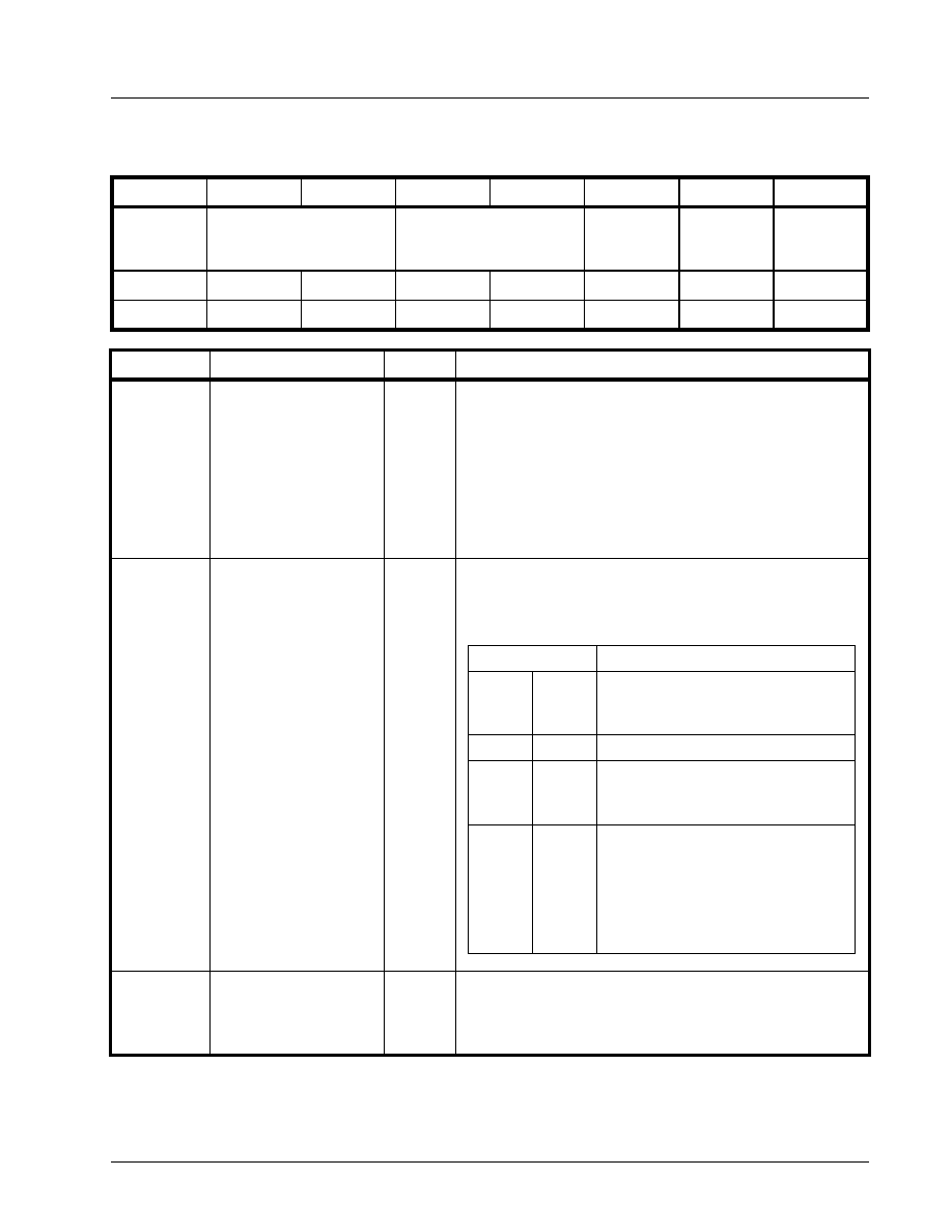
·Á
·Á
·Á
·Á
PRELIMINARY
XRT79L71
1 - CHANNEL DS3/E3 ATM UNI/PPP COMBO IC
REV. P1.0.3
203
TRANSMIT E3, ITU-T G.751 RELATED REGISTERS
TXE3 CONFIGURATION REGISTER - G.751 (DIRECT ADDRESS = 0X1130)
B
IT
7
B
IT
6
B
IT
5
B
IT
4
B
IT
3
B
IT
2
B
IT
1
B
IT
0
TxBIP-4
Enable
TxASrcSel[1:0]
TxNSrcSel[1:0]
TxAIS Enable
TxLOS
Enable
TxFAS
Source
Sel
R/W
R/W
R/W
R/W
R/W
R/W
R/W
R/W
0
0
0
0
0
0
0
0
B
IT
N
UMBER
N
AME
T
YPE
D
ESCRIPTION
7
TxBIP-4 Enable
R/W
Transmit BIP-4 Enable:
This READ/WRITE bit-field permits the user to configure the
Frame Generator block to do the following:
a. Compute the BIP-4 value over a given E3 frame.
b. Insert this BIP-4 value into the last nibble-field within the
very next E3 frame.0 - Does not configure this option. In
this case, the last nibble (of each "outbound" E3 frame)
will contain payload data.1 - Configures the Frame
Generator block to compute and insert the BIP-4 value.
6 - 5
TxASrcSel[1:0]
R/W
Transmit A Bit Source Select[1:0]:
These two READ/WRITE bit-fields permit the user to specify the
source or type of data that is being carried via the "A" bits, within
each "outbound" E3 data stream, as indicated below.
4 - 3
TxNSrcSel[1:0]
R/W
Transmit N Bit Source Select[1:0]:
These two READ/WRITE bit-fields permit the user to specify the
source or type of data that is being carried via the "N" bits, within
each "outbound" E3 data stream, as indicated below.
The C om panion F ram e Synchronizer
block. In this case, the A bit w ill transm it
the FEBE indicator to the rem ote term inal
equipm ent. The A bit will be set to "1"
w hen the com panion F ram e Synchronizer
detects a BIP-4 error, and w ill be set to "0"
w hen the Fram e Synchronizer detects un-
erred E3 fram es.
The "A" bit is sourced via the "Payload
D ata Input Interface" block. T his is
discussed in greater detail in Section _.
N ot Valid - D o not use.
The "TxA" bit-field, w ithin the "TxE3
Service Bit" register (D irect Address =
0x1135)
R es u ltin g S o u rc e o f A B it
T x A S rc S e l[1:0 ]
0
0
1
1
0
1
1
0

XRT79L71
PRELIMINARY
·Á
·Á
·Á
·Á
REV. P1.0.3
1 - CHANNEL DS3/E3 ATM UNI/PPP COMBO IC
204
4 - 3
TxNSrcSel[1:0]
R/W
Transmit N Bit Source Select[1:0]:
These two READ/WRITE bit-fields permit the user to specify the
source or type of data that is being carried via the "N" bits, within
each "outbound" E3 data stream, as indicated below.
2
TxAIS Enable
R/W
Transmit AIS Indicator:
This READ/WRITE bit-field permits the user to (by software con-
trol) force the Frame Generator to generate and transmit the AIS
indicator to the remote terminal equipment.
0 - Does not configure the Frame Generator to generate and
transmit the AIS indicator.
1 - Configures the Frame Generator to generate and transmit the
AIS indicator. In this case, the Frame Generator will force all bits
(within the "outbound" E3 data stream) to an "All Ones" pattern.
N
OTE
: This bit-field is ignored if the Frame Generator has been
configured to transmit the LOS pattern.
1
TxLOS Enable
R/W
Transmit LOS (Pattern) Enable:
This READ/WRITE bit-field permits the user to (by software con-
trol) force the Frame Generator block to transmit the LOS (Loss
of Signal) pattern to the remote terminal equipment.
0 - Does not configure the Frame Generator block to generate
and transmit the LOS pattern.
1 - Configures the Frame Generator block to generate and trans-
mit the LOS pattern. In this case, the Frame Generator block will
force all bits (within the "outbound" E3 data stream) to an "All
Zeros" pattern.
0
TxFAS Source Sel
R/W
Transmit FAS Source Select:
This READ/WRITE bit-field permits the user to specify the
source of the FAS (Framing Alignment Signal), to be used in the
"outbound" E3 data-stream, as indicated below.
0 - FAS bits are inserted internally by the Frame Generator block.
1 - FAS bits are sourced by the "Payload Data Input Interface"
block. This is discussed in greater detail in Section _.
The "N " bit is sourced via the "Payload
D ata Input Interface" block. T his is
discussed in greater detail in Section _.
The LAPD Transm itterIn this case, the N
bit w ill function as the LAPD /P M DL
channel.
N ot Valid - D o not use.
The "TxN" bit-field, within the "T xE3
Service Bit" register (D irect Nddress =
0x1135)
R es u ltin g S o u rc e o f N B it
T x N S rc S e l[1 :0]
0
0
1
1
0
1
1
0

·Á
·Á
·Á
·Á
PRELIMINARY
XRT79L71
1 - CHANNEL DS3/E3 ATM UNI/PPP COMBO IC
REV. P1.0.3
205
TXE3 LAPD CONFIGURATION REGISTER - G.751 (DIRECT ADDRESS = 0X1133)
B
IT
7
B
IT
6
B
IT
5
B
IT
4
B
IT
3
B
IT
2
B
IT
1
B
IT
0
Unused
Auto
Retransmit
Reserved
TxLAPD
Message
Length
TxLAPD
Enable
R/O
R/O
R/O
R/O
R/W
R/O
R/W
R/W
0
0
0
0
1
0
0
0
B
IT
N
UMBER
N
AME
T
YPE
D
ESCRIPTION
7 - 4
Unused
R/O
3
Auto Retransmit
R/W
Auto-Retransmit of LAPD Message:
This READ/WRITE bit-field permits the user to configure the
LAPD Transmitter to transmit PMDL messages, repeatedly at
one-second intervals. Once the user enables this feature, and
then commands the LAPD Transmitter to transmit a given PMDL
Message; the LAPD Transmitter will then proceed to transmit this
PMDL Message (based upon the contents within the Transmit
LAPD Message Buffer) repeatedly at one second intervals.
0 - Disables the Auto-Retransmit Feature. In this case, the
PMDL Message will only be transmitted once, afterwards the
LAPD Transmitter will proceed to transmit a continuous stream of
Flag Sequence octets (0x7E) via the DL bits, within each output
DS3 frame. No more PMDL Messages will be transmitted until
the user commands another transmission.
1 - Enables the Auto-Retransmit Feature.In this case, the LAPD
Transmitter will transmit PMDL messages (based upon the con-
tents within the Transmit LAPD Buffer) repeatedly at one-second
intervals.
N
OTE
: This bit-field is ignored if the LAPD Transmitter is
disabled.
2
Reserved
R/O
1
TxLAPD Message
Length
R/W
Transmit LAPD Message Length Select:
This READ/WRITE bit-field permits the user to specify the length
of the payload data within the outbound LAPD/PMDL Message,
as indicated below.
0 - Configures the LAPD Transmitter to transmit a LAPD/PMDL
message that has a payload data size of 76 bytes.
1 - Configures the LAPD Transmitter to transmit a LAPD/PMDL
message that has a payload data size of 82 bytes.
0
TxLAPD Enable
R/W
LAPD Transmitter Enable:
This READ/WRITE bit-field permits the user to enable the LAPD
Transmitter, within the channel. Once the user enables the
LAPD Transmitter, it will immediately begin transmitting the Flag
Sequence octet (0x7E) to the remote terminal via the outbound
"DL" bits, within each DS3 data stream. The LAPD Transmitter
will continue to do this until the user commands the LAPD Trans-
mitter to transmit a PMDL Message.
0 - Disables the LAPD Transmitter.
1 - Enables the LAPD Transmitter.

XRT79L71
PRELIMINARY
·Á
·Á
·Á
·Á
REV. P1.0.3
1 - CHANNEL DS3/E3 ATM UNI/PPP COMBO IC
206
TXE3 LAPD STATUS/INTERRUPT REGISTER - G.751 (DIRECT ADDRESS = 0X1134)
B
IT
7
B
IT
6
B
IT
5
B
IT
4
B
IT
3
B
IT
2
B
IT
1
B
IT
0
Unused
TxDL Start
TxDL Busy
TxLAPD
Interrupt
Enable
TxLAPD
Interrupt
Status
R/O
R/O
R/O
R/O
R/W
R/O
R/W
RUR
0
0
0
0
0
0
0
0
B
IT
N
UMBER
N
AME
T
YPE
D
ESCRIPTION
7 - 4
Unused
R/O
3
TxDL Start
R/W
Transmit LAPD Message Command:
A "0" to "1" transition, within this bit-field commands the LAPD
Transmitter to begin the following activities:
∑
Reading out the contents of the Transmit LAPD Message
Buffer.
∑
Zero-Stuffing of this data
∑
FCS Calculation and Insertion
∑
Fragmentation of this composite PMDL Message, and
insertion into the "DL" bit-fields, within each outbound DS3
frame.
2
TxDL Busy
R/O
Transmit LAPD Controller Busy Indicator:
This "READ-ONLY" bit-field indicates whether or not the Transmit
LAPD Controller is currently busy transmitting a PMDL Message
to the remote terminal equipment. The user can continuously
poll this bit-field in order to check for completion of transmission
of the LAPD/PMDL Message.
0 - LAPD Transmitter is NOT busy transmitting a PMDL Mes-
sage.
1 - LAPD Transmitter is currently busy transmitting a PMDL Mes-
sage.
1
TxLAPD Interrupt Enable
R/W
Transmit LAPD Interrupt Enable:
This READ/WRITE bit-field permits the user to either enable or
disable the "Transmit LAPD Interrupt". If the user enables this
interrupt, then the channel will generate an interrupt anytime the
LAPD Transmitter has completed its transmission of a given
LAPD/PMDL Message to the remote terminal.
0 - Disables Transmit LAPD Interrupt.
1 - Enables Transmit LAPD Interrupt.
0
TxLAPD Interrupt Status
RUR
Transmit LAPD Interrupt Status:
This RESET-upon-READ bit-field indicates whether or not the
"Transmit LAPD Interrupt" has occurred since the last read of
this register.
0 - Transmit LAPD Interrupt has NOT occurred since the last
read of this register.
1 - Transmit LAPD Interrupt has occurred since the last read of
this register.

·Á
·Á
·Á
·Á
PRELIMINARY
XRT79L71
1 - CHANNEL DS3/E3 ATM UNI/PPP COMBO IC
REV. P1.0.3
207
TXE3 SERVICE BITS REGISTER - G.751 (DIRECT ADDRESS = 0X1135)
B
IT
7
B
IT
6
B
IT
5
B
IT
4
B
IT
3
B
IT
2
B
IT
1
B
IT
0
Unused
TxA
TxN
R/O
R/O
R/O
R/O
R/O
R/O
R/W
R/W
0
0
0
0
0
0
0
0
B
IT
N
UMBER
N
AME
T
YPE
D
ESCRIPTION
7 - 2
Unused
R/O
1
TxA
R/W
Transmit A Bit:
This READ/WRITE bit-field permits the user to control the state
of the "A" bit, within each "outbound" E3 frame, as indicated
below.
0 - Forces each A bit (within the "outbound" E3 frame) to "0".
1 - Forces each A bit (within the "outbound" E3 frame) to "1".
N
OTE
: This bit-field is only valid if the Frame Generator block
has been configured to use this bit-field as the source of
the "A" bit (e.g., if "TxASrcSel[1:0] = "0, 0").
0
TxN
R/W
Transmit N Bit:
This READ/WRITE bit-field permits the user to control the state
of the "N" bit, within each "outbound" E3 frame, as indicated
below.
0 - Forces each N bit (within the "outbound" E3 frame) to "0".
1 - Forces each N bit (within the "outbound" E3 frame) to "1".
N
OTE
: This bit-field is only valid if the Frame Generator block
has been configured to use this bit-field as the source of
the "N" bit (e.g., if "TxNSrcSel[1:0] = "0, 0").

XRT79L71
PRELIMINARY
·Á
·Á
·Á
·Á
REV. P1.0.3
1 - CHANNEL DS3/E3 ATM UNI/PPP COMBO IC
208
TXE3 FAS ERROR MASK UPPER REGISTER - G.751 (INDIRECT ADDRESS =0XNE, 0X48; DIRECT
ADDRESS = 0X1148)
B
IT
7
B
IT
6
B
IT
5
B
IT
4
B
IT
3
B
IT
2
B
IT
1
B
IT
0
Unused
TxFAS_Error_Mask_Upper[4:0]
R/O
R/O
R/O
R/W
R/W
R/W
R/W
R/W
0
0
0
0
0
0
0
0
B
IT
N
UMBER
N
AME
T
YPE
D
ESCRIPTION
7 - 5
Unused
R/O
4 - 0
TxFAS_Error_Mask_
Upper[4:0]
R/W
TxFAS Error Mask Upper[4:0]:
These READ/WRITE bit-fields permit the user to insert bit errors
into the upper five bits, within the FAS (Framing Alignment Sig-
nal), within the outbound E3 data stream.
The Frame Generator will perform an XOR operation with the
contents of these FAS bits, and this register. The results of this
calculation will be inserted into the upper 5 FAS bit positions
within the "outbound" E3 data stream. For each bit-field (within
this register) that is set to "1", the corresponding bit, within the
FAS will be in error.
N
OTE
: For normal operation, the user should set this register to
0x00.
TXE3 FAS ERROR MASK LOWER REGISTER - G.751 (INDIRECT ADDRESS =0XNE, 0X49; DIRECT
ADDRESS = 0X1149)
B
IT
7
B
IT
6
B
IT
5
B
IT
4
B
IT
3
B
IT
2
B
IT
1
B
IT
0
Unused
TxFAS_Error_Mask_Lower[4:0]
R/O
R/O
R/O
R/W
R/W
R/W
R/W
R/W
0
0
0
0
0
0
0
0
B
IT
N
UMBER
N
AME
T
YPE
D
ESCRIPTION
7 - 5
Unused
R/O
4 - 0
TxFAS_Error_Mask_
Lower[4:0]
R/W
TxFAS Error Mask Lower[4:0]:
These READ/WRITE bit-fields permit the user to insert bit errors
into the lower five bits, within the FAS (Framing Alignment Sig-
nal), within the outbound E3 data stream.
The Frame Generator will perform an XOR operation with the
contents of these FAS bits, and this register. The results of this
calculation will be inserted into the lower 5 FAS bit positions
within the "outbound" E3 data stream. For each bit-field (within
this register) that is set to "1", the corresponding bit, within the
FAS will be in error.
N
OTE
: For normal operation, the user should set this register to
0x00.

·Á
·Á
·Á
·Á
PRELIMINARY
XRT79L71
1 - CHANNEL DS3/E3 ATM UNI/PPP COMBO IC
REV. P1.0.3
209
TXE3 BIP-4 MASK REGISTER - G.751 (DIRECT ADDRESS = 0X114A)
B
IT
7
B
IT
6
B
IT
5
B
IT
4
B
IT
3
B
IT
2
B
IT
1
B
IT
0
Unused
TxBIP-4_Mask[3:0]
R/O
R/O
R/O
R/O
R/W
R/W
R/W
R/W
0
0
0
0
0
0
0
0
B
IT
N
UMBER
N
AME
T
YPE
D
ESCRIPTION
7 - 4
Unused
R/O
3 - 0
TxBIP-4_Mask_[3:0]
R/W
TxBIP-4 Error Mask[3:0]:
These READ/WRITE bit-fields permit the user to insert bit errors
into the BIP-4 bits, within the outbound E3 data stream.
The Frame Generator will perform an XOR operation with the
contents of the BIP-4 bits, and this register. The results of this
calculation will be inserted into the BIP-4 bit positions within the
"outbound" E3 data stream. For each bit-field (within this regis-
ter) that is set to "1", the corresponding bit, within the BIP-4 will
be in error.
N
OTE
: For normal operation, the user should set this register to
0x00.

XRT79L71
PRELIMINARY
·Á
·Á
·Á
·Á
REV. P1.0.3
1 - CHANNEL DS3/E3 ATM UNI/PPP COMBO IC
210
TRANSMIT E3, ITU-T G.832 RELATED REGISTERS
TXE3 CONFIGURATION REGISTER - G.832 (DIRECT ADDRESS = 0X1130)
B
IT
7
B
IT
6
B
IT
5
B
IT
4
B
IT
3
B
IT
2
B
IT
1
B
IT
0
Unused
TxDL in NR
Reserved
TxAIS Enable
TxLOS
Enable
TxMA Rx
R/O
R/O
R/O
R/W
R/O
R/W
R/W
R/W
0
0
0
0
0
0
0
0
B
IT
N
UMBER
N
AME
T
YPE
D
ESCRIPTION
7 - 5
Unused
R/O
4
TxDL in NR
R/W
Transmit DL (Data Link Channel) in NR Byte:
This READ/WRITE bit-field permits the user to configure the
Frame Generator to use either the NR or the GC byte as the
LAPD/PMDL channel.
0 - Configures the Frame Generator to transmit all "outbound"
LAPD/PMDL Messages via the GC byte.
1 - Configures the Frame Generator to transmit all "outbound"
LAPD/PMDL Messages via the NR byte.
3
Unused
R/O
2
TxAIS Enable
R/W
Transmit AIS Indicator:
This READ/WRITE bit-field permits the user to (by software con-
trol) force the Frame Generator to generate and transmit the AIS
indicator to the remote terminal equipment.
0 - Does not configure the Frame Generator to generate and
transmit the AIS indicator.
1 - Configures the Frame Generator to generate and transmit the
AIS indicator. In this case, the Frame Generator will force all bits
(within the "outbound" E3 data stream) to an "All Ones" pattern.
N
OTE
: This bit-field is ignored if the Frame Generator has been
configured to transmit the LOS pattern.
1
TxLOS Enable
R/W
Transmit LOS (Pattern) Enable:
This READ/WRITE bit-field permits the user to (by software con-
trol) force the Frame Generator block to transmit the LOS (Loss
of Signal) pattern to the remote terminal equipment.
0 - Does not configure the Frame Generator block to generate
and transmit the LOS pattern.
1 - Configures the Frame Generator block to generate and trans-
mit the LOS pattern. In this case, the Frame Generator block will
force all bits (within the "outbound" E3 data stream) to an "All
Zeros" pattern.

·Á
·Á
·Á
·Á
PRELIMINARY
XRT79L71
1 - CHANNEL DS3/E3 ATM UNI/PPP COMBO IC
REV. P1.0.3
211
0
TxMA Rx
R/W
Transmit MA Byte from Receiver (Frame Synchronizer)
Select:
This READ/WRITE bit-field permits the user to configure the
Frame Generator block to use either the Frame Synchronizer
block or the "Tx MA Byte" Register as the source of the FERF
and FEBE bit-fields (within the MA byte-field of the "outbound"
E3 data stream); as indicated below.
0 - Configures the Frame Generator to read in the contents of the
"Tx MA Byte" register (Direct Address = 0x1136), and write it into
the "MA" byte-field within each "outbound" E3 frame.
N
OTE
: This option permits the user to send FERF and FEBE
indicators, under software control.
1 - Configures the Frame Generator to set the FERF and FEBE
bit-fields to values, based upon conditions detected by the com-
panion Frame Synchronizer block.
B
IT
N
UMBER
N
AME
T
YPE
D
ESCRIPTION

XRT79L71
PRELIMINARY
·Á
·Á
·Á
·Á
REV. P1.0.3
1 - CHANNEL DS3/E3 ATM UNI/PPP COMBO IC
212
TXE3 LAPD CONFIGURATION REGISTER - G.832 (DIRECT ADDRESS = 0X1133)
B
IT
7
B
IT
6
B
IT
5
B
IT
4
B
IT
3
B
IT
2
B
IT
1
B
IT
0
Unused
Auto
Retransmit
Reserved
TxLAPD
Message
Length
TxLAPD
Enable
R/O
R/O
R/O
R/O
R/W
R/O
R/W
R/W
0
0
0
0
1
0
0
0
B
IT
N
UMBER
N
AME
T
YPE
D
ESCRIPTION
7 - 4
Unused
R/O
3
Auto Retransmit
R/W
Auto-Retransmit of LAPD Message:
This READ/WRITE bit-field permits the user to configure the
LAPD Transmitter to transmit PMDL messages, repeatedly at
one-second intervals. Once the user enables this feature, and
then commands the LAPD Transmitter to transmit a given PMDL
Message; the LAPD Transmitter will then proceed to transmit this
PMDL Message (based upon the contents within the Transmit
LAPD Message Buffer) repeatedly at one second intervals.
0 - Disables the Auto-Retransmit Feature. In this case, the
PMDL Message will only be transmitted once, afterwards the
LAPD Transmitter will proceed to transmit a continuous stream of
Flag Sequence octets (0x7E) via the DL bits, within each output
DS3 frame. No more PMDL Messages will be transmitted until
the user commands another transmission.
1 - Enables the Auto-Retransmit Feature.In this case, the LAPD
Transmitter will transmit PMDL messages (based upon the con-
tents within the Transmit LAPD Buffer) repeatedly at one-second
intervals.
N
OTE
: This bit-field is ignored if the LAPD Transmitter is
disabled.
2
Reserved
R/O
1
TxLAPD Message
Length
R/W
Transmit LAPD Message Length Select:
This READ/WRITE bit-field permits the user to specify the length
of the payload data within the outbound LAPD/PMDL Message,
as indicated below.
0 - Configures the LAPD Transmitter to transmit a LAPD/PMDL
message that has a payload data size of 76 bytes.
1 - Configures the LAPD Transmitter to transmit a LAPD/PMDL
message that has a payload data size of 82 bytes.
0
TxLAPD Enable
R/W
LAPD Transmitter Enable:
This READ/WRITE bit-field permits the user to enable the LAPD
Transmitter, within the channel. Once the user enables the
LAPD Transmitter, it will immediately begin transmitting the Flag
Sequence octet (0x7E) to the remote terminal via the outbound
"DL" bits, within each DS3 data stream. The LAPD Transmitter
will continue to do this until the user commands the LAPD Trans-
mitter to transmit a PMDL Message.
0 - Disables the LAPD Transmitter.
1 - Enables the LAPD Transmitter.

·Á
·Á
·Á
·Á
PRELIMINARY
XRT79L71
1 - CHANNEL DS3/E3 ATM UNI/PPP COMBO IC
REV. P1.0.3
213
TXE3 LAPD STATUS/INTERRUPT REGISTER - G.832 (DIRECT ADDRESS = 0X1134)
B
IT
7
B
IT
6
B
IT
5
B
IT
4
B
IT
3
B
IT
2
B
IT
1
B
IT
0
Unused
TxDL Start
TxDL Busy
TxLAPD
Interrupt
Enable
TxLAPD
Interrupt
Status
R/O
R/O
R/O
R/O
R/W
R/O
R/W
RUR
0
0
0
0
0
0
0
0
B
IT
N
UMBER
N
AME
T
YPE
D
ESCRIPTION
7 - 4
Unused
R/O
3
TxDL Start
R/W
Transmit LAPD Message Command:
A "0" to "1" transition, within this bit-field commands the LAPD
Transmitter to begin the following activities:
∑
Reading out the contents of the Transmit LAPD Message
Buffer.
∑
Zero-Stuffing of this data
∑
FCS Calculation and Insertion
∑
Fragmentation of this composite PMDL Message, and
insertion into the "DL" bit-fields, within each outbound DS3
frame.
2
TxDL Busy
R/O
Transmit LAPD Controller Busy Indicator:
This "READ-ONLY" bit-field indicates whether or not the Transmit
LAPD Controller is currently busy transmitting a PMDL Message
to the remote terminal equipment. The user can continuously
poll this bit-field in order to check for completion of transmission
of the LAPD/PMDL Message.
0 - LAPD Transmitter is NOT busy transmitting a PMDL Mes-
sage.
1 - LAPD Transmitter is currently busy transmitting a PMDL Mes-
sage.
1
TxLAPD Interrupt Enable
R/W
Transmit LAPD Interrupt Enable:
This READ/WRITE bit-field permits the user to either enable or
disable the "Transmit LAPD Interrupt". If the user enables this
interrupt, then the channel will generate an interrupt anytime the
LAPD Transmitter has completed its transmission of a given
LAPD/PMDL Message to the remote terminal.
0 - Disables Transmit LAPD Interrupt.
1 - Enables Transmit LAPD Interrupt.
0
TxLAPD Interrupt Status
RUR
Transmit LAPD Interrupt Status:
This RESET-upon-READ bit-field indicates whether or not the
"Transmit LAPD Interrupt" has occurred since the last read of
this register.
0 - Transmit LAPD Interrupt has NOT occurred since the last
read of this register.
1 - Transmit LAPD Interrupt has occurred since the last read of
this register.

XRT79L71
PRELIMINARY
·Á
·Á
·Á
·Á
REV. P1.0.3
1 - CHANNEL DS3/E3 ATM UNI/PPP COMBO IC
214
TXE3 GC BYTE REGISTER - G.832 (DIRECT ADDRESS = 0X1135)
B
IT
7
B
IT
6
B
IT
5
B
IT
4
B
IT
3
B
IT
2
B
IT
1
B
IT
0
TxGC_Byte[7:0]
R/W
R/W
R/W
R/W
R/W
R/W
R/W
R/W
0
0
0
0
0
0
0
0
B
IT
N
UMBER
N
AME
T
YPE
D
ESCRIPTION
7 - 0
TxGC_Byte[7:0]
R/W
Transmit GC Byte:
This READ/WRITE bit-field permits the user to specify the con-
tents of the GC byte, within the "outbound" E3 data stream. The
Frame Generator block will load the contents of this register in
the GC byte-field, within each outbound E3 frame.
N
OTE
: This register is ignored if the GC byte is configured to be
the "LAPD/PMDL" channel.
TXE3 MA BYTE REGISTER - G.832 (DIRECT ADDRESS = 0X1136)
B
IT
7
B
IT
6
B
IT
5
B
IT
4
B
IT
3
B
IT
2
B
IT
1
B
IT
0
TxMA Byte[7:0]
R/W
R/W
R/W
R/W
R/W
R/W
R/W
R/W
0
0
0
1
0
0
0
0
B
IT
N
UMBER
N
AME
T
YPE
D
ESCRIPTION
7 - 0
TxMA_Byte[7:0]
R/W
Transmit MA Byte:
This READ/WRITE bit-field permits the user to specify the con-
tents of the MA byte, within the "outbound" E3 data stream. The
Frame Generator block will load the contents of this register in
the MA byte-field, within each outbound E3 frame.
N
OTES
:
1.
This register is ignored if the "Transmit MA Byte - from
Receiver" option is selected (e.g., by setting "TxMA Rx
= 1").
2.
This feature permits the user to transmit FERF and
FEBE indicators upon software command.

·Á
·Á
·Á
·Á
PRELIMINARY
XRT79L71
1 - CHANNEL DS3/E3 ATM UNI/PPP COMBO IC
REV. P1.0.3
215
TXE3 NR BYTE REGISTER - G.832 (DIRECT ADDRESS = 0X1137)
B
IT
7
B
IT
6
B
IT
5
B
IT
4
B
IT
3
B
IT
2
B
IT
1
B
IT
0
TxNR_Byte[7:0]
R/W
R/W
R/W
R/W
R/W
R/W
R/W
R/W
0
0
0
0
0
0
0
0
B
IT
N
UMBER
N
AME
T
YPE
D
ESCRIPTION
7 - 0
TxNR_Byte[7:0]
R/W
Transmit NR Byte:
This READ/WRITE bit-field permits the user to specify the con-
tents of the NR byte, within the "outbound" E3 data stream. The
Frame Generator block will load the contents of this register in
the NR byte-field, within each outbound E3 frame.
N
OTE
: This register is ignored if the NR byte is configured to be
the "LAPD/PMDL" channel.
TXE3 TTB-0 REGISTER - G.832 (DIRECT ADDRESS = 0X1138)
B
IT
7
B
IT
6
B
IT
5
B
IT
4
B
IT
3
B
IT
2
B
IT
1
B
IT
0
TxTTB_Byte_0
R/W
R/W
R/W
R/W
R/W
R/W
R/W
R/W
1
0
0
0
0
0
0
0
B
IT
N
UMBER
N
AME
T
YPE
D
ESCRIPTION
7 - 0
TxTTB_Byte_0[7:0]
R/W
Transmit TTB (Trail-Trace Buffer) Byte 0:
These READ/WRITE bits permit the user to specify the contents
of "Trail-Trace Buffer Byte 0" within the outbound E3 data stream.
By default, the MSB (Most Significant Bit) of this register bit will
be set to "1" in order to permit the remote terminal to be able to
identify this particular byte, as being the first byte of the "Trail-
Trace Buffer" Message.
TXE3 TTB-1 REGISTER - G.832 (DIRECT ADDRESS = 0X1139)
B
IT
7
B
IT
6
B
IT
5
B
IT
4
B
IT
3
B
IT
2
B
IT
1
B
IT
0
TxTTB_Byte_1
R/W
R/W
R/W
R/W
R/W
R/W
R/W
R/W
0
0
0
0
0
0
0
0
B
IT
N
UMBER
N
AME
T
YPE
D
ESCRIPTION
7 - 0
TxTTB_Byte_1[7:0]
R/W
Transmit TTB (Trail-Trace Buffer) Byte 1:
These READ/WRITE bits permit the user to specify the contents
of "Trail-Trace Buffer Byte 1" within the outbound E3 data stream.
XRT79L71
PRELIMINARY
·Á
·Á
·Á
·Á
REV. P1.0.3
1 - CHANNEL DS3/E3 ATM UNI/PPP COMBO IC
216
TXE3 TTB-2 REGISTER - G.832 (DIRECT ADDRESS = 0X113A)
B
IT
7
B
IT
6
B
IT
5
B
IT
4
B
IT
3
B
IT
2
B
IT
1
B
IT
0
TxTTB_Byte_2
R/W
R/W
R/W
R/W
R/W
R/W
R/W
R/W
0
0
0
0
0
0
0
0
B
IT
N
UMBER
N
AME
T
YPE
D
ESCRIPTION
7 - 0
TxTTB_Byte_2[7:0]
R/W
Transmit TTB (Trail-Trace Buffer) Byte 2:
These READ/WRITE bits permit the user to specify the contents
of "Trail-Trace Buffer Byte 2" within the outbound E3 data stream.
TXE3 TTB-3 REGISTER - G.832 (DIRECT ADDRESS = 0X113B)
B
IT
7
B
IT
6
B
IT
5
B
IT
4
B
IT
3
B
IT
2
B
IT
1
B
IT
0
TxTTB_Byte_3
R/W
R/W
R/W
R/W
R/W
R/W
R/W
R/W
0
0
0
0
0
0
0
0
B
IT
N
UMBER
N
AME
T
YPE
D
ESCRIPTION
7 - 0
TxTTB_Byte_3[7:0]
R/W
Transmit TTB (Trail-Trace Buffer) Byte 3:
These READ/WRITE bits permit the user to specify the contents
of "Trail-Trace Buffer Byte 3" within the outbound E3 data stream.
TXE3 TTB-4 REGISTER - G.832 (DIRECT ADDRESS = 0X113C)
B
IT
7
B
IT
6
B
IT
5
B
IT
4
B
IT
3
B
IT
2
B
IT
1
B
IT
0
TxTTB_Byte_4
R/W
R/W
R/W
R/W
R/W
R/W
R/W
R/W
0
0
0
0
0
0
0
0
B
IT
N
UMBER
N
AME
T
YPE
D
ESCRIPTION
7 - 0
TxTTB_Byte_4[7:0]
R/W
Transmit TTB (Trail-Trace Buffer) Byte 4:
These READ/WRITE bits permit the user to specify the contents
of "Trail-Trace Buffer Byte 4" within the outbound E3 data stream.
·Á
·Á
·Á
·Á
PRELIMINARY
XRT79L71
1 - CHANNEL DS3/E3 ATM UNI/PPP COMBO IC
REV. P1.0.3
217
TXE3 TTB-5 REGISTER - G.832 (DIRECT ADDRESS = 0X113D)
B
IT
7
B
IT
6
B
IT
5
B
IT
4
B
IT
3
B
IT
2
B
IT
1
B
IT
0
TxTTB_Byte_5
R/W
R/W
R/W
R/W
R/W
R/W
R/W
R/W
0
0
0
0
0
0
0
0
B
IT
N
UMBER
N
AME
T
YPE
D
ESCRIPTION
7 - 0
TxTTB_Byte_5[7:0]
R/W
Transmit TTB (Trail-Trace Buffer) Byte 5:
These READ/WRITE bits permit the user to specify the contents
of "Trail-Trace Buffer Byte 5" within the outbound E3 data stream.
TXE3 TTB-6 REGISTER - G.832 (DIRECT ADDRESS = 0X113E)
B
IT
7
B
IT
6
B
IT
5
B
IT
4
B
IT
3
B
IT
2
B
IT
1
B
IT
0
TxTTB_Byte_6
R/W
R/W
R/W
R/W
R/W
R/W
R/W
R/W
0
0
0
0
0
0
0
0
B
IT
N
UMBER
N
AME
T
YPE
D
ESCRIPTION
7 - 0
TxTTB_Byte_6[7:0]
R/W
Transmit TTB (Trail-Trace Buffer) Byte 6:
These READ/WRITE bits permit the user to specify the contents
of "Trail-Trace Buffer Byte 6" within the outbound E3 data stream.
TXE3 TTB-7 REGISTER - G.832 (DIRECT ADDRESS = 0X113F)
B
IT
7
B
IT
6
B
IT
5
B
IT
4
B
IT
3
B
IT
2
B
IT
1
B
IT
0
TxTTB_Byte_7
R/W
R/W
R/W
R/W
R/W
R/W
R/W
R/W
0
0
0
0
0
0
0
0
B
IT
N
UMBER
N
AME
T
YPE
D
ESCRIPTION
7 - 0
TxTTB_Byte_7[7:0]
R/W
Transmit TTB (Trail-Trace Buffer) Byte 7:
These READ/WRITE bits permit the user to specify the contents
of "Trail-Trace Buffer Byte 7" within the outbound E3 data stream.

XRT79L71
PRELIMINARY
·Á
·Á
·Á
·Á
REV. P1.0.3
1 - CHANNEL DS3/E3 ATM UNI/PPP COMBO IC
218
TXE3 TTB-8 REGISTER - G.832 (DIRECT ADDRESS = 0X1140)
B
IT
7
B
IT
6
B
IT
5
B
IT
4
B
IT
3
B
IT
2
B
IT
1
B
IT
0
TxTTB_Byte_8
R/W
R/W
R/W
R/W
R/W
R/W
R/W
R/W
0
0
0
0
0
0
0
0
B
IT
N
UMBER
N
AME
T
YPE
D
ESCRIPTION
7 - 0
TxTTB_Byte_8[7:0]
R/W
Transmit TTB (Trail-Trace Buffer) Byte 8:
These READ/WRITE bits permit the user to specify the contents
of "Trail-Trace Buffer Byte 8" within the outbound E3 data stream.
TXE3 TTB-9 REGISTER - G.832 (DIRECT ADDRESS = 0X1141)
B
IT
7
B
IT
6
B
IT
5
B
IT
4
B
IT
3
B
IT
2
B
IT
1
B
IT
0
TxTTB_Byte_9
R/W
R/W
R/W
R/W
R/W
R/W
R/W
R/W
0
0
0
0
0
0
0
0
B
IT
N
UMBER
N
AME
T
YPE
D
ESCRIPTION
7 - 0
TxTTB_Byte_9[7:0]
R/W
Transmit TTB (Trail-Trace Buffer) Byte 9:
These READ/WRITE bits permit the user to specify the contents
of "Trail-Trace Buffer Byte 9" within the outbound E3 data stream.
TXE3 TTB-10 REGISTER - G.832 (DIRECT ADDRESS = 0X1142)
B
IT
7
B
IT
6
B
IT
5
B
IT
4
B
IT
3
B
IT
2
B
IT
1
B
IT
0
TxTTB_Byte_10
R/W
R/W
R/W
R/W
R/W
R/W
R/W
R/W
0
0
0
0
0
0
0
0
B
IT
N
UMBER
N
AME
T
YPE
D
ESCRIPTION
7 - 0
TxTTB_Byte_10[7:0]
R/W
Transmit TTB (Trail-Trace Buffer) Byte 10:
These READ/WRITE bits permit the user to specify the contents
of "Trail-Trace Buffer Byte 10" within the outbound E3 data
stream.

·Á
·Á
·Á
·Á
PRELIMINARY
XRT79L71
1 - CHANNEL DS3/E3 ATM UNI/PPP COMBO IC
REV. P1.0.3
219
TXE3 TTB-11 REGISTER - G.832 (DIRECT ADDRESS = 0X1143)
B
IT
7
B
IT
6
B
IT
5
B
IT
4
B
IT
3
B
IT
2
B
IT
1
B
IT
0
TxTTB_Byte_11
R/W
R/W
R/W
R/W
R/W
R/W
R/W
R/W
0
0
0
0
0
0
0
0
B
IT
N
UMBER
N
AME
T
YPE
D
ESCRIPTION
7 - 0
TxTTB_Byte_11[7:0]
R/W
Transmit TTB (Trail-Trace Buffer) Byte 11:
These READ/WRITE bits permit the user to specify the contents
of "Trail-Trace Buffer Byte 11" within the outbound E3 data
stream.
TXE3 TTB-12 REGISTER - G.832 (DIRECT ADDRESS = 0X1144)
B
IT
7
B
IT
6
B
IT
5
B
IT
4
B
IT
3
B
IT
2
B
IT
1
B
IT
0
TxTTB_Byte_12
R/W
R/W
R/W
R/W
R/W
R/W
R/W
R/W
0
0
0
0
0
0
0
0
B
IT
N
UMBER
N
AME
T
YPE
D
ESCRIPTION
7 - 0
TxTTB_Byte_12[7:0]
R/W
Transmit TTB (Trail-Trace Buffer) Byte 12:
These READ/WRITE bits permit the user to specify the contents
of "Trail-Trace Buffer Byte 12" within the outbound E3 data
stream.
TXE3 TTB-13 REGISTER - G.832 (DIRECT ADDRESS = 0X1145)
B
IT
7
B
IT
6
B
IT
5
B
IT
4
B
IT
3
B
IT
2
B
IT
1
B
IT
0
TxTTB_Byte_13
R/W
R/W
R/W
R/W
R/W
R/W
R/W
R/W
0
0
0
0
0
0
0
0
B
IT
N
UMBER
N
AME
T
YPE
D
ESCRIPTION
7 - 0
TxTTB_Byte_13[7:0]
R/W
Transmit TTB (Trail-Trace Buffer) Byte 13:
These READ/WRITE bits permit the user to specify the contents
of "Trail-Trace Buffer Byte 13" within the outbound E3 data
stream.
TXE3 TTB-14 REGISTER - G.832 (DIRECT ADDRESS = 0X1146)
B
IT
7
B
IT
6
B
IT
5
B
IT
4
B
IT
3
B
IT
2
B
IT
1
B
IT
0
TxTTB_Byte_14
R/W
R/W
R/W
R/W
R/W
R/W
R/W
R/W
0
0
0
0
0
0
0
0

XRT79L71
PRELIMINARY
·Á
·Á
·Á
·Á
REV. P1.0.3
1 - CHANNEL DS3/E3 ATM UNI/PPP COMBO IC
220
B
IT
N
UMBER
N
AME
T
YPE
D
ESCRIPTION
7 - 0
TxTTB_Byte_14[7:0]
R/W
Transmit TTB (Trail-Trace Buffer) Byte 14:
These READ/WRITE bits permit the user to specify the contents
of "Trail-Trace Buffer Byte 14" within the outbound E3 data
stream.
TXE3 TTB-15 REGISTER - G.832 (DIRECT ADDRESS = 0X1147)
B
IT
7
B
IT
6
B
IT
5
B
IT
4
B
IT
3
B
IT
2
B
IT
1
B
IT
0
TxTTB_Byte_15
R/W
R/W
R/W
R/W
R/W
R/W
R/W
R/W
0
0
0
0
0
0
0
0
B
IT
N
UMBER
N
AME
T
YPE
D
ESCRIPTION
7 - 0
TxTTB_Byte_15[7:0]
R/W
Transmit TTB (Trail-Trace Buffer) Byte 15:
These READ/WRITE bits permit the user to specify the contents
of "Trail-Trace Buffer Byte 15" within the outbound E3 data
stream.
TXE3 FA1 ERROR MASK REGISTER - G.832 (DIRECT ADDRESS = 0X1148)
B
IT
7
B
IT
6
B
IT
5
B
IT
4
B
IT
3
B
IT
2
B
IT
1
B
IT
0
TxFA1_Mask_Byte[7:0]
R/W
R/W
R/W
R/W
R/W
R/W
R/W
R/W
0
0
0
0
0
0
0
0
B
IT
N
UMBER
N
AME
T
YPE
D
ESCRIPTION
7 - 0
TxFA1_Mask_Byte[7:0]
R/W
TxFA1 Error Mask Byte[7:0]:
These READ/WRITE bit-fields permit the user to insert bit errors
into the FA1 bytes, within the outbound E3 data stream.
The Frame Generator will perform an XOR operation with the
contents of the FA1 byte, and this register. The results of this
calculation will be inserted into the FA1 byte position within the
"outbound" E3 data stream. For each bit-field (within this regis-
ter) that is set to "1", the corresponding bit, within the FA1 byte
will be in error.
N
OTE
: For normal operation, the user should set this register to
0x00.

·Á
·Á
·Á
·Á
PRELIMINARY
XRT79L71
1 - CHANNEL DS3/E3 ATM UNI/PPP COMBO IC
REV. P1.0.3
221
TXE3 FA2 ERROR MASK REGISTER - G.832 (DIRECT ADDRESS = 0X1149)
B
IT
7
B
IT
6
B
IT
5
B
IT
4
B
IT
3
B
IT
2
B
IT
1
B
IT
0
TxFA2_Mask_Byte[7:0]
R/W
R/W
R/W
R/W
R/W
R/W
R/W
R/W
0
0
0
0
0
0
0
0
B
IT
N
UMBER
N
AME
T
YPE
D
ESCRIPTION
7 - 0
TxFA2_Mask_Byte[7:0]
R/W
TxFA2 Error Mask Byte[7:0]:
These READ/WRITE bit-fields permit the user to insert bit errors
into the FA2 bytes, within the outbound E3 data stream.
The Frame Generator will perform an XOR operation with the
contents of the FA2 byte, and this register. The results of this
calculation will be inserted into the FA2 byte position within the
"outbound" E3 data stream. For each bit-field (within this regis-
ter) that is set to "1", the corresponding bit, within the FA2 byte
will be in error.
N
OTE
: For normal operation, the user should set this register to
0x00.
TXE3 BIP-8 ERROR MASK REGISTER - G.832 (DIRECT ADDRESS = 0X114A)
B
IT
7
B
IT
6
B
IT
5
B
IT
4
B
IT
3
B
IT
2
B
IT
1
B
IT
0
TxBIP-8_Mask_Byte[7:0]
R/W
R/W
R/W
R/W
R/W
R/W
R/W
R/W
0
0
0
0
0
0
0
0
B
IT
N
UMBER
N
AME
T
YPE
D
ESCRIPTION
7 - 0
TxBIP-8_Mask_Byte[7:0]
R/W
TxBIP-8 (B1) Error Mask[7:0]:
These READ/WRITE bit-fields permit the user to insert bit errors
into the B1 bytes, within the outbound E3 data stream.
The Frame Generator will perform an XOR operation with the
contents of the B1 byte, and this register. The results of this cal-
culation will be inserted into the B1 byte position within the "out-
bound" E3 data stream. For each bit-field (within this register)
that is set to "1", the corresponding bit, within the B1 byte will be
in error.
N
OTE
: For normal operation, the user should set this register to
0x00.
TXE3 SSM REGISTER - G.832 (DIRECT ADDRESS = 0X114B)
B
IT
7
B
IT
6
B
IT
5
B
IT
4
B
IT
3
B
IT
2
B
IT
1
B
IT
0
TxSSM
Enable
Unused
TxSSM[3:0]
R/W
R/O
R/O
R/O
R/W
R/W
R/W
R/W
0
0
0
0
0
0
0
0

XRT79L71
PRELIMINARY
·Á
·Á
·Á
·Á
REV. P1.0.3
1 - CHANNEL DS3/E3 ATM UNI/PPP COMBO IC
222
B
IT
N
UMBER
N
AME
T
YPE
D
ESCRIPTION
7
TxSSM Enable
R/W
Transmit SSM Enable:
This READ/WRITE bit-field permits the user to configure the
Frame Generator block to operate in either the "Old ITU-T G.832
Framing" format or in the "New ITU-T G.832 Framing" format.
0 - Configures the Frame Generator block to support the "Pre
October 1998" version of the E3, ITU-T G.832 framing format.
1 - Configures the Frame Generator block to support the "Octo-
ber 1998" version of the E3, ITU-T G.832 framing format.
6 - 4
Unused
R/O
3 - 0
TxSSM[3:0]
R/W
Transmit Synchronization Status Message[3:0]:
These READ/WRITE bit-fields permit the user to exercise soft-
ware control over the contents of the "SSM" bits, within the MA
byte of the "outbound" E3 data-stream.
N
OTE
: These bit-fields are only active if the DS3/E3 Frame
Generator block is active, and if Bit 7 (TxSSM Enable) of
this register is set to "1".

·Á
·Á
·Á
·Á
PRELIMINARY
XRT79L71
1 - CHANNEL DS3/E3 ATM UNI/PPP COMBO IC
REV. P1.0.3
223
PERFORMANCE MONITOR REGISTERS
PMON EXCESSIVE ZERO COUNT REGISTERS - MSB (DIRECT ADDRESS = 0X114E)
B
IT
7
B
IT
6
B
IT
5
B
IT
4
B
IT
3
B
IT
2
B
IT
1
B
IT
0
PMON_EXZ_Count_Upper_Byte[7:0]
RUR
RUR
RUR
RUR
RUR
RUR
RUR
RUR
0
0
0
0
0
0
0
0
B
IT
N
UMBER
N
AME
T
YPE
D
ESCRIPTION
7 - 0
PMON_EXZ_Count_
Upper_Byte[7:0]
RUR
Performance Monitor - Excessive Zero Event Count - Upper
Byte:
These RESET-upon-READ bits, along with that within the
"PMON Excessive Zero Count Register - LSB" combine to reflect
the cumulative number of instances that a string of three or more
consecutive zeros (for DS3 applications) or four or more consec-
utive zeros (for E3 applications) has been detected by the "Pri-
mary Frame Synchronizer" block since the last read of this
register.
This register contains the Most Significant byte of this 16-bit
expression.
N
OTE
: This register is only valid if the Primary Frame
Synchronizer block has been configured to operate in
the Ingress Path.
PMON EXCESSIVE ZERO COUNT REGISTERS - LSB (DIRECT ADDRESS = 0X114F)
B
IT
7
B
IT
6
B
IT
5
B
IT
4
B
IT
3
B
IT
2
B
IT
1
B
IT
0
PMON_EXZ_Count_Lower_Byte[7:0]
RUR
RUR
RUR
RUR
RUR
RUR
RUR
RUR
0
0
0
0
0
0
0
0
B
IT
N
UMBER
N
AME
T
YPE
D
ESCRIPTION
7 - 0
PMON_EXZ_Count_
Upper_Byte[7:0]
RUR
Performance Monitor - Excessive Zero Event Count - Lower
Byte:
These RESET-upon-READ bits, along with that within the
"PMON Excessive Zero Count Register - MSB" combine to
reflect the cumulative number of instances that a string of three
or more consecutive zeros (for DS3 applications) or four or more
consecutive zeros (for E3 applications) has been detected by the
"Primary Frame Synchronizer" block since the last read of this
register.
This register contains the Least Significant byte of this 16-bit
expression.
N
OTE
: This register is only valid if the Primary Frame
Synchronizer block has been configured to operate in
the Ingress Path.
XRT79L71
PRELIMINARY
·Á
·Á
·Á
·Á
REV. P1.0.3
1 - CHANNEL DS3/E3 ATM UNI/PPP COMBO IC
224
PMON LINE CODE VIOLATION COUNT REGISTERS - MSB (DIRECT ADDRESS = 0X1150)
B
IT
7
B
IT
6
B
IT
5
B
IT
4
B
IT
3
B
IT
2
B
IT
1
B
IT
0
PMON_LCV_Count_Upper_Byte[7:0]
RUR
RUR
RUR
RUR
RUR
RUR
RUR
RUR
0
0
0
0
0
0
0
0
B
IT
N
UMBER
N
AME
T
YPE
D
ESCRIPTION
7 - 0
PMON LCV Count Upper
Byte[7:0]
RUR
Performance Monitor- Line Code Violation Count Register -
Upper Byte:
These RESET-upon-READ bits along with that within the "PMON
Line Code Violation Count - LSB" combine to reflect the cumula-
tive number of Line Code Violations that have been detected by
the Primary Frame Synchronizer block, since the last read of this
register.
This register contains the Most Significant byte of this 16-bit
expression.
N
OTE
: This register is only valid if the Primary Frame
Synchronizer block has been configured to operate in
the Ingress Path.
PMON LINE CODE VIOLATION COUNT REGISTERS - LSB (DIRECT ADDRESS = 0X1151)
B
IT
7
B
IT
6
B
IT
5
B
IT
4
B
IT
3
B
IT
2
B
IT
1
B
IT
0
PMON_LCV_Count_Lower_Byte[7:0]
RUR
RUR
RUR
RUR
RUR
RUR
RUR
RUR
0
0
0
0
0
0
0
0
B
IT
N
UMBER
N
AME
T
YPE
D
ESCRIPTION
7 - 0
PMON LCV Count Lower
Byte[7:0]
RUR
Performance Monitor- Line Code Violation Count Register -
Lower Byte:
These RESET-upon-READ bits along with that within the "PMON
Line Code Violation Count - MSB" combine to reflect the cumula-
tive number of Line Code Violations that have been detected by
the Primary Frame Synchronizer block, since the last read of this
register.
This register contains the Least Significant byte of this 16-bit
expression.
N
OTE
: This register is only valid if the Primary Frame
Synchronizer block has been configured to operate in
the Ingress Path.

·Á
·Á
·Á
·Á
PRELIMINARY
XRT79L71
1 - CHANNEL DS3/E3 ATM UNI/PPP COMBO IC
REV. P1.0.3
225
PMON FRAMING BIT/BYTE ERROR COUNT REGISTER - MSB (DIRECT ADDRESS = 0X1152)
B
IT
7
B
IT
6
B
IT
5
B
IT
4
B
IT
3
B
IT
2
B
IT
1
B
IT
0
PMON_Framing_Bit/Byte_Error_Count_Upper_Byte[7:0]
RUR
RUR
RUR
RUR
RUR
RUR
RUR
RUR
0
0
0
0
0
0
0
0
B
IT
N
UMBER
N
AME
T
YPE
D
ESCRIPTION
7 - 0
PMON_Framing Bit/Byte
Error_Count_Upper
Byte[7:0]
RUR
Performance Monitor - Framing Bit/Byte Error Count - Upper
Byte:
These RESET-upon-READ bits, along with that within the
"PMON Framing Bit/Byte Error Count Register - LSB" combine
to reflect the cumulative number of Framing bit (or byte) errors
that have been detected by the Primary Frame Synchronizer
block, since the last read of this register.
This register contains the Most Significant byte of this 16-bit
expression.
N
OTES
:
1.
For DS3 applications, this register will increment for
each F or M bit error detected.
2.
For E3, ITU-T G.751 applications, this register will
increment for each FAS error detected.
3.
For E3, ITU-T G.832 applications, this register will
increment for each FA1 or FA2 byte error detected.
4.
These register bits are not active if the Primary Frame
Synchronizer block has been by-passed.

XRT79L71
PRELIMINARY
·Á
·Á
·Á
·Á
REV. P1.0.3
1 - CHANNEL DS3/E3 ATM UNI/PPP COMBO IC
226
PMON FRAMING BIT/BYTE ERROR COUNT REGISTER - LSB (DIRECT ADDRESS = 0X1153)
B
IT
7
B
IT
6
B
IT
5
B
IT
4
B
IT
3
B
IT
2
B
IT
1
B
IT
0
PMON_Framing_Bit/Byte_Error_Count_Lower_Byte[7:0]
RUR
RUR
RUR
RUR
RUR
RUR
RUR
RUR
0
0
0
0
0
0
0
0
B
IT
N
UMBER
N
AME
T
YPE
D
ESCRIPTION
7 - 0
PMON_Framing Bit/Byte
Error_Count_Lower
Byte[7:0]
RUR
Performance Monitor - Framing Bit/Byte Error Count - Lower
Byte:
These RESET-upon-READ bits, along with that within the
"PMON Framing Bit/Byte Error Count Register - MSB" combine
to reflect the cumulative number of Framing bit (or byte) errors
that have been detected by the Primary Frame Synchronizer
block, since the last read of this register.
This register contains the Least Significant byte of this 16-bit
expression.
N
OTES
:
1.
For DS3 applications, this register will increment for
each F or M bit error detected.
2.
For E3, ITU-T G.751 applications, this register will
increment for each FAS error detected.
3.
For E3, ITU-T G.832 applications, this register will
increment for each FA1 or FA2 byte error detected.
4.
These register bits are not active if the Primary Frame
Synchronizer block has been by-passed.
PMON PARITY/P-BIT ERROR COUNT REGISTER - MSB (DIRECT ADDRESS = 0X1154)
B
IT
7
B
IT
6
B
IT
5
B
IT
4
B
IT
3
B
IT
2
B
IT
1
B
IT
0
PMON_Parity_Error_Count_Upper_Byte[7:0]
RUR
RUR
RUR
RUR
RUR
RUR
RUR
RUR
0
0
0
0
0
0
0
0
B
IT
N
UMBER
N
AME
T
YPE
D
ESCRIPTION
7 - 0
PMON_P-Bit/Parity Bit
Error_Count_Upper
Byte[7:0]
RUR
Performance Monitor - P Bit/Parity Bit Error Count - Upper
Byte:
These RESET-upon-READ bits, along with that within the
"PMON P-Bit/Parity Bit Error Count Register - LSB" combine to
reflect the cumulative number of P bit errors (for DS3 applica-
tions) or BIP-8/BIP-4 errors (for E3 applications) that have been
detected by the Primary Frame Synchronizer block, since the
last read of this register.
This register contains the Most Significant byte of this 16-bit
expression.
N
OTE
: These register bits are not active if the Primary Frame
Synchronizer block has been by-passed.

·Á
·Á
·Á
·Á
PRELIMINARY
XRT79L71
1 - CHANNEL DS3/E3 ATM UNI/PPP COMBO IC
REV. P1.0.3
227
PMON PARITY/P-BIT ERROR COUNT REGISTER - LSB (DIRECT ADDRESS = 0X1155)
B
IT
7
B
IT
6
B
IT
5
B
IT
4
B
IT
3
B
IT
2
B
IT
1
B
IT
0
PMON_Parity_Error_Count_Lower_Byte[7:0]
RUR
RUR
RUR
RUR
RUR
RUR
RUR
RUR
0
0
0
0
0
0
0
0
B
IT
N
UMBER
N
AME
T
YPE
D
ESCRIPTION
7 - 0
PMON_P-Bit/Parity Bit
Error_Count_Lower
Byte[7:0]
RUR
Performance Monitor - P Bit/Parity Bit Error Count - Lower
Byte:
These RESET-upon-READ bits, along with that within the
"PMON P-Bit/Parity Bit Error Count Register - MSB" combine to
reflect the cumulative number of P bit errors (for DS3 applica-
tions) or BIP-8/BIP-4 errors (for E3 applications) that have been
detected by the Primary Frame Synchronizer block, since the
last read of this register.
This register contains the Least Significant byte of this 16-bit
expression.
N
OTE
: These register bits are not active if the Primary Frame
Synchronizer block has been by-passed.
PMON FEBE EVENT COUNT REGISTER - MSB (DIRECT ADDRESS = 0X1156)
B
IT
7
B
IT
6
B
IT
5
B
IT
4
B
IT
3
B
IT
2
B
IT
1
B
IT
0
PMON_FEBE_Event_Count_Upper_Byte[7:0]
RUR
RUR
RUR
RUR
RUR
RUR
RUR
RUR
0
0
0
0
0
0
0
0
B
IT
N
UMBER
N
AME
T
YPE
D
ESCRIPTION
7 - 0
PMON_FEBE
Event_Count_Upper
Byte[7:0]
RUR
Performance Monitor - FEBE Event Count - Upper Byte:
These RESET-upon-READ bits, along with that within the
"PMON FEBE Event Count Register - LSB" combine to reflect
the cumulative number of "erred" FEBE events that have been
detected by the Primary Frame Synchronizer block, since the
last read of this register.
This register contains the Most Significant byte of this 16-bit
expression.
N
OTE
: These register bits are not active if the Primary Frame
Synchronizer block has been by-passed.

XRT79L71
PRELIMINARY
·Á
·Á
·Á
·Á
REV. P1.0.3
1 - CHANNEL DS3/E3 ATM UNI/PPP COMBO IC
228
PMON FEBE EVENT COUNT REGISTER - LSB (DIRECT ADDRESS = 0X1157)
B
IT
7
B
IT
6
B
IT
5
B
IT
4
B
IT
3
B
IT
2
B
IT
1
B
IT
0
PMON_FEBE_Event_Count_Lower_Byte[7:0]
RUR
RUR
RUR
RUR
RUR
RUR
RUR
RUR
0
0
0
0
0
0
0
0
B
IT
N
UMBER
N
AME
T
YPE
D
ESCRIPTION
7 - 0
PMON_FEBE
Event_Count_Lower
Byte[7:0]
RUR
Performance Monitor - FEBE Event Count - Lower Byte:
These RESET-upon-READ bits, along with that within the
"PMON FEBE Event Count Register - MSB" combine to reflect
the cumulative number of "erred" FEBE events that have been
detected by the Primary Frame Synchronizer block, since the
last read of this register.
This register contains the Least Significant byte of this 16-bit
expression.
N
OTE
: These register bits are not active if the Primary Frame
Synchronizer block has been by-passed.
PMON CP-BIT ERROR COUNT REGISTER - MSB (DIRECT ADDRESS = 0X1158)
B
IT
7
B
IT
6
B
IT
5
B
IT
4
B
IT
3
B
IT
2
B
IT
1
B
IT
0
PMON_CP-Bit_Error_Count_Upper_Byte[7:0]
RUR
RUR
RUR
RUR
RUR
RUR
RUR
RUR
0
0
0
0
0
0
0
0
B
IT
N
UMBER
N
AME
T
YPE
D
ESCRIPTION
7 - 0
PMON_CP-Bit
Error_Count_Upper
Byte[7:0]
RUR
Performance Monitor - CP Bit Error Count - Upper Byte:
These RESET-upon-READ bits, along with that within the
"PMON CP-Bit Error Count Register - LSB" combine to reflect
the cumulative number of CP bit errors that have been detected
by the Primary Frame Synchronizer block, since the last read of
this register.
This register contains the Most Significant byte of this 16-bit
expression.
N
OTE
: These register bits are not active if the Primary Frame
Synchronizer block has been by-passed, or if the Frame
Synchronizer has not been configured to operate in the
DS3 C-Bit Parity Framing format.

·Á
·Á
·Á
·Á
PRELIMINARY
XRT79L71
1 - CHANNEL DS3/E3 ATM UNI/PPP COMBO IC
REV. P1.0.3
229
PMON CP-BIT ERROR COUNT REGISTER - LSB (DIRECT ADDRESS = 0X1159)
B
IT
7
B
IT
6
B
IT
5
B
IT
4
B
IT
3
B
IT
2
B
IT
1
B
IT
0
PMON_CP-Bit_Error_Count_Lower_Byte[7:0]
RUR
RUR
RUR
RUR
RUR
RUR
RUR
RUR
0
0
0
0
0
0
0
0
B
IT
N
UMBER
N
AME
T
YPE
D
ESCRIPTION
7 - 0
PMON_CP-Bit
Error_Count_Lower
Byte[7:0]
RUR
Performance Monitor - CP Bit Error Count - Lower Byte:
These RESET-upon-READ bits, along with that within the
"PMON CP-Bit Error Count Register - MSB" combine to reflect
the cumulative number of CP bit errors that have been detected
by the Primary Frame Synchronizer block, since the last read of
this register.
This register contains the Least Significant byte of this 16-bit
expression.
N
OTE
: These register bits are not active if the Primary Frame
Synchronizer block has been by-passed, or if the Frame
Synchronizer has not been configured to operate in the
DS3 C-Bit Parity Framing Format.
PRBS ERROR COUNT REGISTER - MSB (DIRECT ADDRESS = 0X1168)
B
IT
7
B
IT
6
B
IT
5
B
IT
4
B
IT
3
B
IT
2
B
IT
1
B
IT
0
PRBS_Error_Count_Upper_Byte[7:0]
RUR
RUR
RUR
RUR
RUR
RUR
RUR
RUR
0
0
0
0
0
0
0
0
B
IT
N
UMBER
N
AME
T
YPE
D
ESCRIPTION
7 - 0
PRBS
Error_Count_Upper
Byte[7:0]
RUR
PRBS Error Count - Upper Byte:
These RESET-upon-READ bits, along with that within the "PRBS
Error Count Register - LSB" combine to reflect the cumulative
number of PRBS bit errors that have been detected by the Pri-
mary Frame Synchronizer block, since the last read of this regis-
ter.
This register contains the Most Significant byte of this 16-bit
expression.
N
OTE
: These register bits are not active if the Primary Frame
Synchronizer block has been by-passed, and if the
PRBS Receiver has not been enabled.
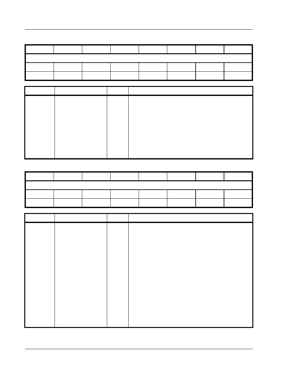
XRT79L71
PRELIMINARY
·Á
·Á
·Á
·Á
REV. P1.0.3
1 - CHANNEL DS3/E3 ATM UNI/PPP COMBO IC
230
PRBS ERROR COUNT REGISTER - LSB (DIRECT ADDRESS = 0X1169)
B
IT
7
B
IT
6
B
IT
5
B
IT
4
B
IT
3
B
IT
2
B
IT
1
B
IT
0
PRBS_Error_Count_Lower_Byte[7:0]
RUR
RUR
RUR
RUR
RUR
RUR
RUR
RUR
0
0
0
0
0
0
0
0
B
IT
N
UMBER
N
AME
T
YPE
D
ESCRIPTION
7 - 0
PRBS
Error_Count_Lower
Byte[7:0]
RUR
PRBS Error Count - Lower Byte:
These RESET-upon-READ bits, along with that within the "PRBS
Error Count Register - MSB" combine to reflect the cumulative
number of PRBS bit errors that have been detected by the Pri-
mary Frame Synchronizer block, since the last read of this regis-
ter.
This register contains the Least Significant byte of this 16-bit
expression.
N
OTE
: These register bits are not active if the Primary Frame
Synchronizer block has been by-passed, and if the
PRBS Receiver has not been enabled.
PMON HOLDING REGISTER (DIRECT ADDRESS = 0X116C)
B
IT
7
B
IT
6
B
IT
5
B
IT
4
B
IT
3
B
IT
2
B
IT
1
B
IT
0
PMON_Hold_Value[7:0]
R/O
R/O
R/O
R/O
R/O
R/O
R/O
R/O
0
0
0
0
0
0
0
0
B
IT
N
UMBER
N
AME
T
YPE
D
ESCRIPTION
7 - 0
PMON Holding Value
R/O
PMON Holding Value:
These READ-ONLY bit-fields were specifically allocated to sup-
port READ operations to the PMON (Performance Monitor) Reg-
isters, within the DS3/E3 Framer blocks.
Since the PMON Register (within the DS3/E3 Framer block) are
16-bit registers. Therefore, given that the bi-directional data bus
of the XRT79L71 is only 8-bits wide, it will require two read oper-
ations in order to read out the entire 16 bit content of these regis-
ters.
The other thing to note is that the PMON Registers (within the
DS3/E3 Framer blocks) are RESET-upon-READ type registers.
As consequence, the entire 16-bit contents of a given PMON
Register will be cleared to "0x0000" immediately after the user
has executed the first (of two) read operations to this register. In
order to avoid losing the contents of the other byte, the contents
of the "un-read" byte is automatically loaded into this register.
Hence, once the user reads a register, from a given PMON Reg-
ister, he/she is suppose to obtain the contents of the other byte,
by reading the contents of this register.

·Á
·Á
·Á
·Á
PRELIMINARY
XRT79L71
1 - CHANNEL DS3/E3 ATM UNI/PPP COMBO IC
REV. P1.0.3
231
ONE SECOND ERROR STATUS REGISTER (DIRECT ADDRESS = 0X116D)
B
IT
7
B
IT
6
B
IT
5
B
IT
4
B
IT
3
B
IT
2
B
IT
1
B
IT
0
Unused
Errored Second
Severe Errored Second
R/O
R/O
R/O
R/O
R/O
R/O
R/O
R/O
0
0
0
0
0
0
0
0
B
IT
N
UMBER
N
AME
T
YPE
D
ESCRIPTION
7 - 2
Unused
R/O
1
Errored Second
R/O
Errored Second Indicator:
This READ-ONLY bit-field indicates whether or not the DS3/E3
Framer block has declared the last one-second accumulation
period as a "Errored Second".
The DS3/E3 Framer block will declare a "errored second" if it
detects any of the following events.
For DS3 Applications
∑
P-Bit Errors
∑
CP Bit Errors
∑
Framing Bit (F or M bit) Errors
For E3 Applications
∑
BIP-4/BIP-8 Errors
∑
FAS or Framing Byte (FA1, FA2) Errors
0 - Indicates that the DS3/E3 Framer block has NOT declared
the last one-second accumulation period as being an errored
second.
1 - Indicates that the DS3/E3 Framer block has declared the last
one-second accumulation period as being an errored second.
N
OTE
: This bit-field is only active if the Primary Frame
Synchronizer block is enabled.
0
Severely Errored Second
R/O
Severely Errored Second Indicator:
This READ-ONLY bit-field indicates whether or not the DS3/E3
Framer block has declared the last one second accumulation
period as being a "Severely Errored Second".
The DS3/E3 Framer block will declare a given second as being a
"severely errored" second if it determines that the BER (Bit Error
Rate) during this "one-second accumulation" period is greater
than 10-3 errors/second.
0 - Indicates that the DS3/E3 Framer block has not declared the
last one-second accumulation period as being a "severely-
errored" second.
1 - Indicates that the DS3/E3 Framer block has declared the last
one-second accumulation period as being a "severely-errored"
second.
N
OTE
: This bit-field is only active if the Primary Frame
Synchronizer block is enabled.

XRT79L71
PRELIMINARY
·Á
·Á
·Á
·Á
REV. P1.0.3
1 - CHANNEL DS3/E3 ATM UNI/PPP COMBO IC
232
ONE SECOND - LCV COUNT ACCUMULATOR REGISTER - MSB (DIRECT ADDRESS = 0X116E)
B
IT
7
B
IT
6
B
IT
5
B
IT
4
B
IT
3
B
IT
2
B
IT
1
B
IT
0
One_Second_LCV_Count_Accum_MSB[7:0]
R/O
R/O
R/O
R/O
R/O
R/O
R/O
R/O
0
0
0
0
0
0
0
0
B
IT
N
UMBER
N
AME
T
YPE
D
ESCRIPTION
7 - 0
One_Second_LCV_
Count Accum_LSB[7:0]
R/O
One Second LCV Count Accumulator Register - MSB:
These READ-ONLY bits, along with that within the "One Second
LCV Count Accumulator Register - MSB" combine to reflect the
cumulative number of "Line Code Violations" that have been
detected by the Frame Synchronizer block, in the last "one sec-
ond" accumulation period.
This register contains the Most Significant byte of this 16-bit
expression.
N
OTE
: This register is only valid if the Primary Frame
Synchronizer block has been configured to operate in
the Ingress Path.
ONE SECOND - LCV COUNT ACCUMULATOR REGISTER - LSB (DIRECT ADDRESS = 0X116F)
B
IT
7
B
IT
6
B
IT
5
B
IT
4
B
IT
3
B
IT
2
B
IT
1
B
IT
0
One_Second_LCV_Count_Accum_LSB[7:0]
R/O
R/O
R/O
R/O
R/O
R/O
R/O
R/O
0
0
0
0
0
0
0
0
B
IT
N
UMBER
N
AME
T
YPE
D
ESCRIPTION
7 - 0
One_Second_LCV_
Count Accum_LSB[7:0]
R/O
One Second LCV Count Accumulator Register - LSB:
These READ-ONLY bits, along with that within the "One Second
LCV Count Accumulator Register - LSB" combine to reflect the
cumulative number of "Line Code Violations" that have been
detected by the Frame Synchronizer block, in the last "one sec-
ond" accumulation period.
This register contains the Least Significant byte of this 16-bit
expression.
N
OTE
: This register is only valid if the Primary Frame
Synchronizer block has been configured to operate in
the Ingress Path.

·Á
·Á
·Á
·Á
PRELIMINARY
XRT79L71
1 - CHANNEL DS3/E3 ATM UNI/PPP COMBO IC
REV. P1.0.3
233
ONE SECOND - PARITY ERROR ACCUMULATOR REGISTER - MSB (DIRECT ADDRESS = 0X1170)
B
IT
7
B
IT
6
B
IT
5
B
IT
4
B
IT
3
B
IT
2
B
IT
1
B
IT
0
One_Second_Parity_Error_Accum_MSB[7:0]
R/O
R/O
R/O
R/O
R/O
R/O
R/O
R/O
0
0
0
0
0
0
0
0
B
IT
N
UMBER
N
AME
T
YPE
D
ESCRIPTION
7 - 0
One_Second_Parity
Error Accum_MSB[7:0]
R/O
One Second Parity Error Accumulator Register - MSB:
These READ-ONLY bits, along with that within the "One Second
Parity Error Accumulator Register - LSB" combine to reflect the
cumulative number of "Parity Errors" that have been detected by
the Frame Synchronizer block, in the last "one second" accumu-
lation period.
This register contains the Most Significant byte of this 16-bit
expression.
N
OTES
:
1.
For DS3 applications, the register will reflect the
number of P-bit errors, detected within the last "one
second" accumulation period.
2.
.For E3, ITU-T G.751 applications, this register will
reflect the number of BIP-4 errors, detected within the
last "one second" accumulation period.3
3.
For E3, ITU-T G.832 applications, this register will
reflect the number of BIP-8 (B1 Byte) errors detected
within the last "one second" accumulation period.

XRT79L71
PRELIMINARY
·Á
·Á
·Á
·Á
REV. P1.0.3
1 - CHANNEL DS3/E3 ATM UNI/PPP COMBO IC
234
ONE SECOND - PARITY ERROR ACCUMULATOR REGISTER - LSB (DIRECT ADDRESS = 0X1171)
B
IT
7
B
IT
6
B
IT
5
B
IT
4
B
IT
3
B
IT
2
B
IT
1
B
IT
0
One_Second_Parity_Error_Accum_LSB[7:0]
R/O
R/O
R/O
R/O
R/O
R/O
R/O
R/O
0
0
0
0
0
0
0
0
B
IT
N
UMBER
N
AME
T
YPE
D
ESCRIPTION
7 - 0
One_Second_Parity
Error Accum_LSB[7:0]
R/O
One Second Parity Error Accumulator Register - LSB:
These READ-ONLY bits, along with that within the "One Second
Parity Error Accumulator Register - MSB" combine to reflect the
cumulative number of "Parity Errors" that have been detected by
the Frame Synchronizer block, in the last "one second" accumu-
lation period. This register contains the Least Significant byte of
this 16-bit expression.
N
OTES
:
1.
For DS3 applications, the register will reflect the
number of P-bit errors, detected within the last "one
second" accumulation period.
2.
For E3, ITU-T G.751 applications, this register will
reflect the number of BIP-4 errors, detected within the
last "one second" accumulation period..
3.
For E3, ITU-T G.832 applications, this register will
reflect the number of BIP-8 (B1 Byte) errors detected
within the last "one second" accumulation period.
ONE SECOND - CP BIT ERROR ACCUMULATOR REGISTER - MSB (DIRECT ADDRESS = 0X1172)
B
IT
7
B
IT
6
B
IT
5
B
IT
4
B
IT
3
B
IT
2
B
IT
1
B
IT
0
One_Second_CP_Bit_Error_Accum_MSB[7:0]
R/O
R/O
R/O
R/O
R/O
R/O
R/O
R/O
0
0
0
0
0
0
0
0
B
IT
N
UMBER
N
AME
T
YPE
D
ESCRIPTION
7 - 0
One_Second_CP Bit
Error Accum_MSB[7:0]
R/O
One Second CP Bit Error Accumulator Register - MSB:
These READ-ONLY bits, along with that within the "One Second
CP-Bit Error Accumulator Register - LSB" combine to reflect the
cumulative number of "CP Bit Errors" that have been detected by
the Frame Synchronizer block, in the last "one second" accumu-
lation period.
This register contains the Most Significant byte of this 16-bit
expression.
N
OTE
: This register is inactive if the Frame Synchronizer block is
"by-passed" or if the Frame Synchronizer block has not
been configured to operate in the DS3, C-Bit Parity
framing format.

·Á
·Á
·Á
·Á
PRELIMINARY
XRT79L71
1 - CHANNEL DS3/E3 ATM UNI/PPP COMBO IC
REV. P1.0.3
235
ONE SECOND - CP BIT ERROR ACCUMULATOR REGISTER - LSB (DIRECT ADDRESS = 0X1173)
B
IT
7
B
IT
6
B
IT
5
B
IT
4
B
IT
3
B
IT
2
B
IT
1
B
IT
0
One_Second_CP_Bit_Error_Accum_LSB[7:0]
R/O
R/O
R/O
R/O
R/O
R/O
R/O
R/O
0
0
0
0
0
0
0
0
B
IT
N
UMBER
N
AME
T
YPE
D
ESCRIPTION
7 - 0
One_Second_CP Bit
Error Accum_LSB[7:0]
R/O
One Second CP Bit Error Accumulator Register - LSB:
These READ-ONLY bits, along with that within the "One Second
CP-Bit Error Accumulator Register - MSB" combine to reflect the
cumulative number of "CP Bit Errors" that have been detected by
the Frame Synchronizer block, in the last "one second" accumu-
lation period.
This register contains the Least Significant byte of this 16-bit
expression.
N
OTE
: This register is inactive if the Frame Synchronizer block is
"by-passed" or if the Frame Synchronizer block has not
been configured to operate in the DS3, C-Bit Parity
framing format.

XRT79L71
PRELIMINARY
·Á
·Á
·Á
·Á
REV. P1.0.3
1 - CHANNEL DS3/E3 ATM UNI/PPP COMBO IC
236
GENERAL PURPOSE I/O PIN CONTROL REGISTERS
LINE INTERFACE DRIVE REGISTER (DIRECT ADDRESS = 0X1180)
B
IT
7
B
IT
6
B
IT
5
B
IT
4
B
IT
3
B
IT
2
B
IT
1
B
IT
0
Internal
Remote
Loop-back
Unused
REQB
Output Pin
TAOS
Output Pin
ENCODIS
Output Pin
TxLEV
Output Pin
RLOOP
Output Pin
LLOOP
Output Pin
R/W
R/O
R/W
R/W
R/W
R/W
R/W
R/W
0
0
0
0
1
0
0
0
B
IT
N
UMBER
N
AME
T
YPE
D
ESCRIPTION
7
Internal Remote
Loop-back
R/W
Internal Remote Loop-back Mode:
This READ/WRITE bit-field permits the user to configure the
DS3/E3 Framer block to operate in the "Remote Loop-back"
Mode.
If the user enables this feature, then the Receive Input of the Pri-
mary Frame Synchronizer block will automatically be routed to
the Transmit Output of the Frame Generator block.
0 - Disables the Remote Loop-back Mode.
1 - Enables the Remote Loop-back Mode.
N
OTE
: This feature is only available if both the Frame Generator
and the Primary Frame Synchronizer blocks are
enabled.
6
Unused
R/O
5
REQB Output Pin
R/W
REQB Output Pin control:
This READ/WRITE bit-field permits the user to control the state
of the "REQB" output pin. This output pin can be used to func-
tion as a General Purpose Output pin.
0 - Commands this output pin to toggle and stay "LOW".
1 - Commands this output pin to toggle and stay "HIGH".
4
TAOS Output Pin
R/W
TAOS Output Pin control:
This READ/WRITE bit-field permits the user to control the state
of the "TAOS" output pin. This output pin can be used to function
as a General Purpose Output pin.
0 - Commands this output pin to toggle and stay "LOW".
1 - Commands this output pin to toggle and stay "HIGH".
3
ENCODIS Output Pin
R/W
ENCODIS Output Pin control:
This READ/WRITE bit-field permits the user to control the state
of the "ENCODIS" output pin. This output pin can be used to
function as a General Purpose Output pin.
0 - Commands this output pin to toggle and stay "LOW".
1 - Commands this output pin to toggle and stay "HIGH".
2
TxLEV Output Pin
R/W
TxLEV Output Pin control:
This READ/WRITE bit-field permits the user to control the state
of the "TxLEV" output pin. This output pin can be used to func-
tion as a General Purpose Output pin.
0 - Commands this output pin to toggle and stay "LOW".
1 - Commands this output pin to toggle and stay "HIGH".

·Á
·Á
·Á
·Á
PRELIMINARY
XRT79L71
1 - CHANNEL DS3/E3 ATM UNI/PPP COMBO IC
REV. P1.0.3
237
1
RLOOP Output Pin
R/W
RLOOP Output Pin control:
This READ/WRITE bit-field permits the user to control the state
of the "RLOOP" output pin. This output pin can be used to func-
tion as a General Purpose Output pin.
0 - Commands this output pin to toggle and stay "LOW".
1 - Commands this output pin to toggle and stay "HIGH".
0
LLOOP Output Pin
R/W
LLOOP Output Pin control:
This READ/WRITE bit-field permits the user to control the state
of the "LLOOP" output pin. This output pin can be used to func-
tion as a General Purpose Output pin.
0 - Commands this output pin to toggle and stay "LOW".
1 - Commands this output pin to toggle and stay "HIGH".
B
IT
N
UMBER
N
AME
T
YPE
D
ESCRIPTION

XRT79L71
PRELIMINARY
·Á
·Á
·Á
·Á
REV. P1.0.3
1 - CHANNEL DS3/E3 ATM UNI/PPP COMBO IC
238
LINE INTERFACE SCAN REGISTER (DIRECT ADDRESS = 0X1181)
B
IT
7
B
IT
6
B
IT
5
B
IT
4
B
IT
3
B
IT
2
B
IT
1
B
IT
0
Unused
DMO
Input Pin
RLOL
Input Pin
RLOS
Input Pin
R/O
R/O
R/O
R/O
R/O
R/O
R/0
R/O
0
0
0
0
0
0
0
0
B
IT
N
UMBER
N
AME
T
YPE
D
ESCRIPTION
7 - 3
Unused
R/O
2
DMO Input Pin
R/O
DMO Input Pin:
This READ-ONLY bit-field reflects the state of the "DMO" input
pin, as described below.
0 - The DMO input pin is pulled to the logic "LOW" state.
1 - The DMO input pin is pulled to the logic "HIGH" state.
N
OTE
: The DMO input pin can function as a "General Purpose"
Input pin.
1
RLOL Input Pin
R/O
RLOL Input Pin:
This READ-ONLY bit-field reflects the state of the "RLOL" input
pin, as described below.
0 - The RLOL input pin is pulled to the logic "LOW" state.
1 - The RLOL input pin is pulled to the logic "HIGH" state.
N
OTE
: The RLOL input pin can function as a "General Purpose"
Input pin.
0
RLOS Input Pin
R/O
RLOS Input Pin:
This READ-ONLY bit-field reflects the state of the "RLOS" input
pin, as described below.
0 - The RLOS input pin is pulled to the logic "LOW" state.
1 - The RLOS input pin is pulled to the logic "HIGH" state.
N
OTE
: The RLOS input pin cannot function as a "General
Purpose" Input pin. Pulling the RLOS input pin "HIGH"
will cause the corresponding Channel to declare an LOS
(Loss of Signal)

·Á
·Á
·Á
·Á
PRELIMINARY
XRT79L71
1 - CHANNEL DS3/E3 ATM UNI/PPP COMBO IC
REV. P1.0.3
239
LAPD CONTROLLER BYTE COUNT REGISTERS
TXLAPD BYTE COUNT REGISTER (DIRECT ADDRESS = 0X1183)
B
IT
7
B
IT
6
B
IT
5
B
IT
4
B
IT
3
B
IT
2
B
IT
1
B
IT
0
TxLAPD_MESSAGE_SIZE[7:0]
R/W
R/W
R/W
R/W
R/W
R/W
R/W
R/W
0
0
0
0
0
0
0
0
B
IT
N
UMBER
N
AME
T
YPE
D
ESCRIPTION
7 - 0
TxLAPD_MESSAGE_
SIZE[7:0]
R/W
Transmit LAPD Message Size:
These READ/WRITE bit-fields permit the user to specify the size
of the information payload (in terms of bytes) within the very next
outbound LAPD/PMDL Message, whenever Bit 7 (TxLAPD Any)
within the "Transmit Tx LAPD Configuration" Register has been
set to "1".
RXLAPD BYTE COUNT REGISTER (DIRECT ADDRESS = 0X1184)
B
IT
7
B
IT
6
B
IT
5
B
IT
4
B
IT
3
B
IT
2
B
IT
1
B
IT
0
RxLAPD_MESSAGE_SIZE[7:0]
R/O
R/O
R/O
R/O
R/O
R/O
R/O
R/O
0
0
0
0
0
0
0
0
B
IT
N
UMBER
N
AME
T
YPE
D
ESCRIPTION
7 - 0
RxLAPD_MESSAGE_
SIZE[7:0]
R/O
Receive LAPD Message Size:
These READ-ONLY bit-fields indicate the size of the most
recently received LAPD/PMDL Message, whenever Bit 7
(RxLAPD Any) within the "Rx LAPD Control" Register; has been
set to "1".The contents of these register bits, reflects the
Received LAPD Message size, in terms of bytes.

XRT79L71
PRELIMINARY
·Á
·Á
·Á
·Á
REV. P1.0.3
1 - CHANNEL DS3/E3 ATM UNI/PPP COMBO IC
240
RECEIVE DS3/E3 INTERRUPT STATUS REGISTER - SECONDARY FRAME SYNCHRONIZER BLOCK
(DIRECT ADDRESS = 0X11F9)
B
IT
7
B
IT
6
B
IT
5
B
IT
4
B
IT
3
B
IT
2
B
IT
1
B
IT
0
Unused
Change of
LOS
Condition
Interrupt
Status
Change of
AIS
Condition
Interrupt
Status
Change of
DS3 Idle
Condition
Interrupt
Status
Unused
Change of
OOF
Condition
Interrupt
Status
Unused
R/O
RUR
RUR
RUR
R/O
R/O
RUR
R/O
0
0
0
0
0
0
0
0
B
IT
N
UMBER
N
AME
T
YPE
D
ESCRIPTION
7
Unused
R/O
6
Change of LOS Condition
Interrupt Status
RUR
Change of LOS Condition Interrupt Status:
This RESET-upon-READ bit-field indicates whether or not the
"Change of LOS Condition" Interrupt (per the Secondary Frame
Synchronizer block) has occurred since the last read of this reg-
ister.
0 - Indicates that the "Change of LOS Condition" Interrupt (per
the Secondary Frame Synchronizer block) has NOT occurred
since the last read of this register.
1 - Indicates that the "Change of LOS Condition" Interrupt (per
the Secondary Frame Synchronizer block) has occurred since
the last read of this register.
N
OTE
: The user can determine the current state of "LOS" (per
the Secondary Frame Synchronizer" block) by reading
out the state of Bit 6 (Secondary Frame Synchronizer -
LOS Defect Declared) within the Receive DS3/E3 Status
Register - Secondary Frame Synchronizer block"
register (Direct Address = 0x11F1).
5
Change of AIS Condition
Interrupt Status
RUR
Change of AIS Condition Interrupt Status:
This RESET-upon-READ bit-field indicates whether or not the
"Change of AIS Condition" Interrupt (per the Secondary Frame
Synchronizer block) has occurred since the last read of this reg-
ister.
0 - Indicates that the "Change of AIS Condition" Interrupt (per
the Secondary Frame Synchronizer block) has NOT occurred
since the last read of this register.
1 - Indicates that the "Change of AIS Condition" Interrupt (per
the Secondary Frame Synchronizer block) has occurred since
the last read of this register.
N
OTE
: The user can determine the current state of "LOS" (per
the Secondary Frame Synchronizer" block) by reading
out the state of Bit 7 (Secondary Frame Synchronizer -
AIS Defect Declared) within the Receive DS3/E3 Status
Register - Secondary Frame Synchronizer block"
register (Direct Address = 0x11F1).

·Á
·Á
·Á
·Á
PRELIMINARY
XRT79L71
1 - CHANNEL DS3/E3 ATM UNI/PPP COMBO IC
REV. P1.0.3
241
4
Change of DS3 Idle
Condition Interrupt Status
RUR
Change of DS3 Idle Condition Interrupt Status:
This RESET-upon-READ bit-field indicates whether or not the
"Change of DS3 Idle Condition" Interrupt (per the Secondary
Frame Synchronizer block) has occurred since the last read of
this register.
0 - Indicates that the "Change of DS3 Idle Condition" Interrupt
(per the Secondary Frame Synchronizer block) has NOT
occurred since the last read of this register.
1 - Indicates that the "Change of DS3 Idle Condition" Interrupt
(per the Secondary Frame Synchronizer block) has occurred
since the last read of this register.
N
OTE
: The user can determine the current "DS3 Idle" staet (per
the Secondary Frame Synchronizer" block) by reading
out the state of Bit 5 (Secondary Frame Synchronizer -
DS3 Idle Pattern Detected) within the Receive DS3/E3
Status Register - Secondary Frame Synchronizer block"
register (Direct Address = 0x11F1).
3 - 2
Unused
R/O
1
Change of OOF
Condition Interrupt Status
RUR
Change of OOF Condition Interrupt Status:
This RESET-upon-READ bit-field indicates whether or not the
"Change of OOF Condition" Interrupt (per the Secondary Frame
Synchronizer block) has occurred since the last read of this reg-
ister.
0 - Indicates that the "Change of OOF Condition" Interrupt (per
the Secondary Frame Synchronizer block) has NOT occurred
since the last read of this register.
1 - Indicates that the "Change of OOF Condition" Interrupt (per
the Secondary Frame Synchronizer block) has occurred since
the last read of this register.
N
OTE
: The user can determine the current state of "LOS" (per
the Secondary Frame Synchronizer" block) by reading
out the state of Bit 4 (Secondary Frame Synchronizer -
OOF Defect Declared) within the Receive DS3/E3
Status Register - Secondary Frame Synchronizer block"
register (Direct Address = 0x11F1).
0
Unused
R/O
B
IT
N
UMBER
N
AME
T
YPE
D
ESCRIPTION

XRT79L71
PRELIMINARY
·Á
·Á
·Á
·Á
REV. P1.0.3
1 - CHANNEL DS3/E3 ATM UNI/PPP COMBO IC
242
THE RECEIVE ATM CELL PROCESSOR BLOCK
This section presents the Register Description/Address Map of the control registers associated with the
Receive ATM Cell Processor block.
T
ABLE
17: R
ECEIVE
ATM C
ELL
P
ROCESSOR
/PPP P
ROCESSOR
B
LOCK
- R
EGISTER
/A
DDRESS
M
AP
A
DDRESS
L
OCATION
R
EGISTER
N
AME
T
YPE
D
EFAULT
V
ALUE
R
ECEIVE
ATM C
ELL
P
ROCESSOR
/PPP P
ROCESSOR
B
LOCK
C
ONTROL
R
EGISTERS
0x1700
Receive ATM Control - Receive ATM Control Register - Byte 3
R/W
0x00
0x1701
Receive ATM Control - Receive ATM Control Register - Byte 2
R/W
0x00
0x1702
Receive ATM Control - Receive ATM Control Register - Byte 1
R/W
0x00
0x1703
Receive ATM Cell/PPP Control - Receive ATM Control Register - Byte 0
R/W
0x00
0x1704 - 0x1706
Reserved
R/O
0x00
0x1707
Receive ATM Status Register- -1
R/O
0x00
0x1708 - 0x1709
Reserved
R/O
0x00
0x170A
Receive ATM Interrupt Status Register - Byte 1
RUR
0x00
0x170B
Receive ATM Cell/PPP Processor Interrupt Status Register - Byte 0
RUR
0x00
0x170C - 0x170D
Reserved
R/O
0x00
0x170E
Receive ATM Cell Processor Block Interrupt Enable Register - Byte 1
R/W
0x00
0x170F
Receive ATM Cell/PPP Processor Block Interrupt Enable Register - Byte
0
R/W
0x00
0x1710
Receive PPP Processor - Receive Good PPP Packet Count Register -
Byte 3
RUR
0x00
0x1711
Receive PPP Processor - Receive Good PPP Packet Count Register -
Byte 2
RUR
0x00
0x1712
Receive PPP Processor - Receive Good PPP Packet Count Register -
Byte 1
RUR
0x00
0x1713
Receive ATM Cell Insertion/Extraction Memory Control Register Receive
PPP Processor - Receive Good PPP Packet Count Register - Byte 0
R/W or
RUR
0x00
0x1714
Receive ATM Cell Insertion/Extraction Memory Data Register - Byte 3
Receive PPP Processor - Receive FCS Error Count Register - Byte 3
R/W or
RUR
0x00
0x1715
Receive ATM Cell Insertion/Extraction Memory Data Register - Byte 2
Receive PPP Processor - Receive FCS Error Count Register - Byte 2
R/W or
RUR
0x00
0x1716
Receive ATM Cell Insertion/Extraction Memory Data Register - Byte 1
Receive PPP Processor - Receive FCS Error Count Register - Byte 1
R/W or
RUR
0x00
0x1717
Receive ATM Cell Insertion/Extraction Memory Data Register - Byte 0
Receive PPP Processor - Receive FCS Error Count Register - Byte 0
R/W or
RUR
0x00
0x1718
Receive ATM Programmable User Defined Field Register - Byte 3
Receive PPP Processor - Receive ABORT Count Register - Byte 3
R/W or
RUR
0x00
0x1719
Receive ATM Programmable User Defined Field Register - Byte 2
Receive PPP Processor - Receive ABORT Count Register - Byte 2
R/W or
RUR
0x00

·Á
·Á
·Á
·Á
PRELIMINARY
XRT79L71
1 - CHANNEL DS3/E3 ATM UNI/PPP COMBO IC
REV. P1.0.3
243
0x171A
Receive ATM Programmable User Defined Field Register - Byte 1
Receive PPP Processor - Receive ABORT Count Register - Byte 1
R/W or
RUR
0x00
0x171B
Receive ATM Programmable User Defined Field Register - Byte 0
Receive PPP Processor - Receive ABORT Count Register - Byte 0
R/W or
RUR
0x00
0x171C
Receive PPP Processor - Receive RUNT PPP Count Register - Byte 3
RUR
0x00
0x171D
Receive PPP Processor - Receive RUNT PPP Count Register - Byte 2
RUR
0x00
0x171E
Receive PPP Processor - Receive RUNT PPP Count Register - Byte 1
RUR
0x00
0x171F
Receive PPP Processor - Receive RUNT PPP Count Register - Byte 0
RUR
0x00
0x1720
Receive ATM Controller - Test Cell Header - Byte 1
R/W
0x00
0x1721
Receive ATM Controller - Test Cell Header - Byte 2
R/W
0x00
0x1722
Receive ATM Controller - Test Cell Header - Byte 3
R/W
0x00
0x1723
Receive ATM Controller - Test Cell Header - Byte 4
R/W
0x00
0x1724
Receive ATM Controller - Test Cell Error Counter - Byte 3
RUR
0x00
0x1725
Receive ATM Controller - Test Cell Error Counter - Byte 2
RUR
0x00
0x1726
Receive ATM Controller - Test Cell Error Counter - Byte 1
RUR
0x00
0x1727
Receive ATM Controller - Test Cell Error Counter - Byte 0
RUR
0x00
0x1728
Receive ATM Controller - Receive ATM Cell Count - Byte 3
RUR
0x00
0x1729
Receive ATM Controller - Receive ATM Cell Count - Byte 2
RUR
0x00
0x172A
Receive ATM Controller - Receive ATM Cell Count - Byte 1
RUR
0x00
0x172B
Receive ATM Controller - Receive ATM Cell Count - Byte 0
RUR
0x00
0x172C
Receive ATM Controller - Receive ATM Discard Cell Count - Byte 3
RUR
0x00
0x172D
Receive ATM Controller - Receive ATM Discard Cell Count - Byte 2
RUR
0x00
0x172E
Receive ATM Controller - Receive ATM Discard Cell Count - Byte 1
RUR
0x00
0x172F
Receive ATM Controller - Receive ATM Discard Cell Count - Byte 0
RUR
0x00
0x1730
Receive ATM Controller - Receive ATM Correctable HEC Cell Counter -
Byte 3
RUR
0x00
0x1731
Receive ATM Controller - Receive ATM Correctable HEC Cell Counter -
Byte 2
RUR
0x00
0x1732
Receive ATM Controller - Receive ATM Correctable HEC Cell Counter -
Byte 1
RUR
0x00
0x1733
Receive ATM Controller - Receive ATM Correctable HEC Cell Counter -
Byte 0
RUR
0x00
0x1734
Receive ATM Controller - Receive ATM Uncorrectable HEC Cell Counter -
Byte 3
RUR
0x00
T
ABLE
17: R
ECEIVE
ATM C
ELL
P
ROCESSOR
/PPP P
ROCESSOR
B
LOCK
- R
EGISTER
/A
DDRESS
M
AP
A
DDRESS
L
OCATION
R
EGISTER
N
AME
T
YPE
D
EFAULT
V
ALUE
R
ECEIVE
ATM C
ELL
P
ROCESSOR
/PPP P
ROCESSOR
B
LOCK
C
ONTROL
R
EGISTERS

XRT79L71
PRELIMINARY
·Á
·Á
·Á
·Á
REV. P1.0.3
1 - CHANNEL DS3/E3 ATM UNI/PPP COMBO IC
244
0x1735
Receive ATM Controller - Receive ATM Uncorrectable HEC Cell Counter -
Byte 2
RUR
0x00
0x1736
Receive ATM Controller - Receive ATM Uncorrectable HEC Cell Counter -
Byte 1
RUR
0x00
0x1737
Receive ATM Controller - Receive ATM Uncorrectable HEC Cell Counter -
Byte 0
RUR
0x00
0x1738 - 0x1742
Reserved
R/O
0x00
0x1743
Receive ATM Controller - Receive ATM Filter # 0 Control Register
R/W
0x00
0x1744
Receive ATM Controller - Receive ATM Filter # 0 Pattern - Header Byte 1
R/W
0x00
0x1745
Receive ATM Controller - Receive ATM Filter # 0 Pattern - Header Byte 2
R/W
0x00
0x1746
Receive ATM Controller - Receive ATM Filter # 0 Pattern - Header Byte 3
R/W
0x00
0x1747
Receive ATM Controller - Receive ATM Filter # 0 Pattern - Header Byte 4
R/W
0x00
0x1748
Receive ATM Controller - Receive ATM Filter # 0 Check - Header Byte 1
R/W
0x00
0x1749
Receive ATM Controller - Receive ATM Filter # 0 Check - Header Byte 2
R/W
0x00
0x174A
Receive ATM Controller - Receive ATM Filter # 0 Check - Header Byte 3
R/W
0x00
0x174B
Receive ATM Controller - Receive ATM Filter # 0 Check - Header Byte 4
R/W
0x00
0x174C
Receive ATM Controller - Filter # 0 - Filtered Cell Count Register - Byte 3
R/W
0x00
0x174D
Receive ATM Controller - Filter # 0 - Filtered Cell Count Register - Byte 2
R/W
0x00
0x174E
Receive ATM Controller - Filter # 0 - Filtered Cell Count Register - Byte 1
R/W
0x00
0x174F
Receive ATM Controller - Filter # 0 - Filtered Cell Count Register - Byte 0
R/W
0x00
0x1750 - 0x1752
Reserved
R/O
0x00
0x1753
Receive ATM Controller - Receive ATM Filter # 1 Control Register
R/W
0x00
0x1754
Receive ATM Controller - Receive ATM Filter # 1 Pattern - Header Byte 1
R/W
0x00
0x1755
Receive ATM Controller - Receive ATM Filter # 1 Pattern - Header Byte 2
R/W
0x00
0x1756
Receive ATM Controller - Receive ATM Filter # 1 Pattern - Header Byte 3
R/W
0x00
0x1757
Receive ATM Controller - Receive ATM Filter # 1 Pattern - Header Byte 4
R/W
0x00
0x1758
Receive ATM Controller - Receive ATM Filter # 1 Check - Header Byte 1
R/W
0x00
0x1759
Receive ATM Controller - Receive ATM Filter # 1 Check - Header Byte 2
R/W
0x00
0x175A
Receive ATM Controller - Receive ATM Filter # 1 Check - Header Byte 3
R/W
0x00
0x175B
Receive ATM Controller - Receive ATM Filter # 1 Check - Header Byte 4
R/W
0x00
0x175C
Receive ATM Controller - Filter # 1 - Filtered Cell Count Register - Byte 3
R/W
0x00
0x175D
Receive ATM Controller - Filter # 1 - Filtered Cell Count Register - Byte 2
R/W
0x00
T
ABLE
17: R
ECEIVE
ATM C
ELL
P
ROCESSOR
/PPP P
ROCESSOR
B
LOCK
- R
EGISTER
/A
DDRESS
M
AP
A
DDRESS
L
OCATION
R
EGISTER
N
AME
T
YPE
D
EFAULT
V
ALUE
R
ECEIVE
ATM C
ELL
P
ROCESSOR
/PPP P
ROCESSOR
B
LOCK
C
ONTROL
R
EGISTERS

·Á
·Á
·Á
·Á
PRELIMINARY
XRT79L71
1 - CHANNEL DS3/E3 ATM UNI/PPP COMBO IC
REV. P1.0.3
245
0x175E
Receive ATM Controller - Filter # 1 - Filtered Cell Count Register - Byte 1
R/W
0x00
0x175F
Receive ATM Controller - Filter # 1 - Filtered Cell Count Register - Byte 0
R/W
0x00
0x1760 - 0x1762
Reserved
R/O
0x00
0x1763
Receive ATM Controller - Receive ATM Filter # 2 Control Register
R/W
0x00
0x1764
Receive ATM Controller - Receive ATM Filter # 2 Pattern - Header Byte 1
R/W
0x00
0x1765
Receive ATM Controller - Receive ATM Filter # 2 Pattern - Header Byte 2
R/W
0x00
0x1766
Receive ATM Controller - Receive ATM Filter # 2 Pattern - Header Byte 3
R/W
0x00
0x1767
Receive ATM Controller - Receive ATM Filter # 2 Pattern - Header Byte 4
R/W
0x00
0x1768
Receive ATM Controller - Receive ATM Filter # 2 Check - Header Byte 1
R/W
0x00
0x1769
Receive ATM Controller - Receive ATM Filter # 2 Check - Header Byte 2
R/W
0x00
0x176A
Receive ATM Controller - Receive ATM Filter # 2 Check - Header Byte 3
R/W
0x00
0x176B
Receive ATM Controller - Receive ATM Filter # 2 Check - Header Byte 4
R/W
0x00
0x176C
Receive ATM Controller - Filter # 2 - Filtered Cell Count Register - Byte 3
R/W
0x00
0x176D
Receive ATM Controller - Filter # 2 - Filtered Cell Count Register - Byte 2
R/W
0x00
0x176E
Receive ATM Controller - Filter # 2 - Filtered Cell Count Register - Byte 1
R/W
0x00
0x176F
Receive ATM Controller - Filter # 2 - Filtered Cell Count Register - Byte 0
R/W
0x00
0x1770 - 0x1772
Reserved
R/O
0x00
0x1773
Receive ATM Controller - Receive ATM Filter # 3 Control Register
R/W
0x00
0x1774
Receive ATM Controller - Receive ATM Filter # 3 Pattern - Header Byte 1
R/W
0x00
0x1775
Receive ATM Controller - Receive ATM Filter # 3 Pattern - Header Byte 2
R/W
0x00
0x1776
Receive ATM Controller - Receive ATM Filter # 3 Pattern - Header Byte 3
R/W
0x00
0x1777
Receive ATM Controller - Receive ATM Filter # 3 Pattern - Header Byte 4
R/W
0x00
0x1778
Receive ATM Controller - Receive ATM Filter # 3 Check - Header Byte 1
R/W
0x00
0x1779
Receive ATM Controller - Receive ATM Filter # 3 Check - Header Byte 2
R/W
0x00
0x177A
Receive ATM Controller - Receive ATM Filter # 3 Check - Header Byte 3
R/W
0x00
0x177B
Receive ATM Controller - Receive ATM Filter # 3 Check - Header Byte 4
R/W
0x00
0x177C
Receive ATM Controller - Filter # 3 - Filtered Cell Count Register - Byte 3
R/W
0x00
0x177D
Receive ATM Controller - Filter # 3 - Filtered Cell Count Register - Byte 2
R/W
0x00
0x177E
Receive ATM Controller - Filter # 3 - Filtered Cell Count Register - Byte 1
R/W
0x00
0x177F
Receive ATM Controller - Filter # 3 - Filtered Cell Count Register - Byte 0
R/W
0x00
0x1780 - 0x1901
Reserved
R/O
0x00
T
ABLE
17: R
ECEIVE
ATM C
ELL
P
ROCESSOR
/PPP P
ROCESSOR
B
LOCK
- R
EGISTER
/A
DDRESS
M
AP
A
DDRESS
L
OCATION
R
EGISTER
N
AME
T
YPE
D
EFAULT
V
ALUE
R
ECEIVE
ATM C
ELL
P
ROCESSOR
/PPP P
ROCESSOR
B
LOCK
C
ONTROL
R
EGISTERS

XRT79L71
PRELIMINARY
·Á
·Á
·Á
·Á
REV. P1.0.3
1 - CHANNEL DS3/E3 ATM UNI/PPP COMBO IC
246
RECEIVE ATM CELL PROCESSOR BLOCK - RECEIVE ATM CONTROL REGISTER - BYTE 3 (ADDRESS =
0X1700)
B
IT
7
B
IT
6
B
IT
5
B
IT
4
B
IT
3
B
IT
2
B
IT
1
B
IT
0
RECEIVE ATM CELL PROCESSOR BLOCK - RECEIVE ATM CONTROL REGISTER - BYTE 2 (ADDRESS
= 0X1701)
B
IT
7
B
IT
6
B
IT
5
B
IT
4
B
IT
3
B
IT
2
B
IT
1
B
IT
0
Unused
Receive ATM Cell
Processor Enable
Test Cell Receiver
Mode Enable
R/O
R/O
R/O
R/O
R/O
R/O
R/W
R/W
0
0
0
0
0
0
0
0
B
IT
N
UMBER
N
AME
T
YPE
D
ESCRIPTION
7 - 2
Unused
R/O
1
Receive ATM Cell Pro-
cessor Enable
R/W
Receive ATM Cell Processor Block Enable:
This READ/WRITE bit-field permits the user to either enable or
disable the Receive ATM Cell Processor block. If the user
wishes to operate a given Channel in the ATM Mode, then he/
she must enable the Receive ATM Cell Processor block.
0 - Disables the Receive ATM Cell Processor block.
1 - Enables the Receive ATM Cell Processor block.
0
Test Cell Receiver Mode
Enable
R/W
Test Cell Receiver Mode Enable:
This READ/WRITE bit-field permits the user to enable the Test
Cell Receiver (within the Receive ATM Cell Processor block).
The user must implement this configuration option in order to
perform diagnostic operations with Test Cells.
0 - Disables the Test Cell Receiver.
1 - Enables the Test Cell Receiver.
N
OTE
: For normal operation, the user should set this bit-field to
"1".

·Á
·Á
·Á
·Á
PRELIMINARY
XRT79L71
1 - CHANNEL DS3/E3 ATM UNI/PPP COMBO IC
REV. P1.0.3
247
RECEIVE ATM CELL PROCESSOR BLOCK - RECEIVE ATM CONTROL REGISTER - BYTE 1 (ADDRESS =
0X1702)
B
IT
7
B
IT
6
B
IT
5
B
IT
4
B
IT
3
B
IT
2
B
IT
1
B
IT
0
Unused
GFC Extrac-
tion Enable
HEC Byte
Correction
Enable
Uncorrect-
able HEC
Byte Error
Discard
COSET Poly-
nomial Addi-
tion
Regenerate
HEC Byte
Enable
R/O
R/O
R/O
R/W
R/W
R/W
R/W
R/W
0
0
0
0
1
0
1
0
B
IT
N
UMBER
N
AME
T
YPE
D
ESCRIPTION
7 - 5
Unused
R/O
4
GFC Extraction Enable
R/W
GFC (Generic Flow Control) Extraction Enable:
This READ/WRITE bit-field permits the user to configure the
Receive ATM Cell Processor block to output the contents of the
GFC Nibble (within each incoming ATM Cell) via the Receive
GFC Value Output port.
0 - Configures the Receive ATM Cell Processor block to NOT
output the contents of the GFC Nibble (within each incoming
ATM cell) via the Receive GFC Value Output port.
1 - Configures the Receive ATM Cell Processor block to output
the contents of the GFC Nibble (within each incoming ATM cell)
via the Receive GFC Value Output port.
3
HEC Byte Correction
Enable
R/W
HEC Byte Correction Enable:
This READ/WRITE bit-field permits the user to enable "Correc-
tion Mode" operation for the Receive ATM Cell Processor block.
If the user implements this configuration option, then the Receive
ATM Cell Processor block will transition into either the "Correc-
tion Mode" or the "Detection Mode" (as "Receive Conditions"
warrant).
If the Receive ATM Cell Processor block is operating in the "Cor-
rection Mode" then it will correct any cells that contain "Single-
Bit" Header byte errors.
In contrast, if the Receive ATM Cell Processor block is operating
in the "Detection Mode", then it will unconditionally discard any
cells that contain Header byte errors (Single-Bit or Multi-Bit
errors).
If the user does not implement this feature, then the Receive
ATM Cell Processor block will only be capable of operating in the
"Detection Mode".
0 - Disables the "Correction Mode". In this setting, the Receive
ATM Cell Processor block will only operate in the "Detection
Mode".
1 - Enables the "Correction Mode". In this setting, the Receive
ATM Cell Processor block will transition into and out of the "Cor-
rection Mode" or "Detection Mode" as receive conditions war-
rant.

XRT79L71
PRELIMINARY
·Á
·Á
·Á
·Á
REV. P1.0.3
1 - CHANNEL DS3/E3 ATM UNI/PPP COMBO IC
248
2
Uncorrectable HEC Byte
Discard
R/W
Uncorrectable HEC Byte Discard:
This READ/WRITE bit-field permits the user to configure the
Receive ATM Cell Processor block to either automatically dis-
card all incoming ATM cells that contain "uncorrectable" HEC
byte errors.
If the user implements this feature, then the Receive ATM Cell
Processor block will automatically discard any cells that fit into
any one of the following categories.
∑
ATM cells that contain multi-bit HEC byte errors.
∑
ATM cells that contain single-bit HEC byte errors, while the
Receive ATM Cell Processor block is operating in the
"Detection Mode".
If the user does NOT implement this feature, then the Receive
ATM Cell Processor block will NOT discard any cells that fit into
any one of the above-mentioned categories. These cells (along
with un-erred or cells with "correctable" HEC byte errors) will be
retains for further processing.
0 - Configures the Receive ATM Cell Processor block to retain
ALL ATM cells (even those with "uncorrectable" HEC byte errors)
for further processing.
1 - Configures the Receive ATM Cell Processor block to auto-
matically discard all incoming ATM cells that contain "uncorrect-
able" HEC byte errors. All remaining cells will be retained for
further processing.
1
COSET Polynomial Addi-
tion
R/W
COSET Polynomial Addition:
This READ/WRITE bit-field permits the user to configure the
Receive ATM Cell Processor block to account for the fact that the
HEC bytes (within the incoming ATM cell traffic) also include the
Modulo-2 addition of the Coset Polynomial (e.g., x^6 + x^4 + x^2
+ 1), when performing HEC Byte Verification.
0 - Configures the Receive ATM Cell Processor block to NOT
account for the Coset Polynomial within the HEC bytes of the
incoming ATM cells.
1 - Configures the Receive ATM Cell Processor block to account
for the Coset Polynomial within the HEC bytes of the incoming
ATM cells.
0
Regenerate HEC Byte
Enable
R/W
Regenerate HEC Byte Enable:
This READ/WRITE bit-field permits the user to configure the
Receive ATM Cell Processor block to automatically re-compute
and insert a new HEC byte into each incoming ATM cell that con-
tains an uncorrectable HEC byte.
0 - Does not configure the Receive ATM Cell Processor block to
compute and insert a new HEC byte into ATM cells that contains
an "uncorrectable" HEC byte error.
1 - Configures the Receive ATM Cell Processor block to compute
and insert a new HEC byte into any incoming ATM cell that con-
tains an "uncorrectable" HEC byte error.
N
OTE
: If the user wishes to implement this feature, then he/she
must disable the "Uncorrectable HEC Byte Discard"
feature, by setting Bit 2 (Uncorrectable HEC Byte
Discard) within this register, to "0".
B
IT
N
UMBER
N
AME
T
YPE
D
ESCRIPTION
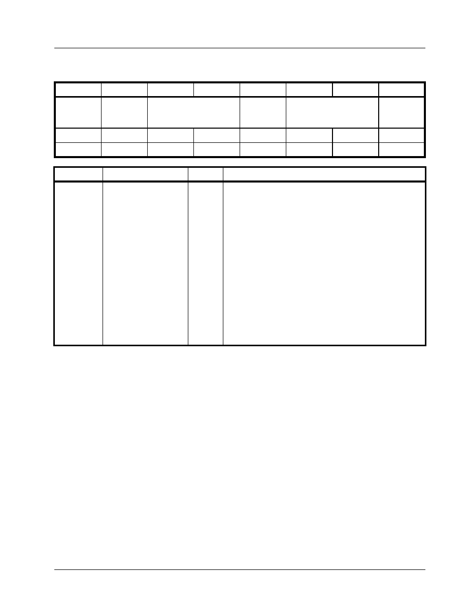
·Á
·Á
·Á
·Á
PRELIMINARY
XRT79L71
1 - CHANNEL DS3/E3 ATM UNI/PPP COMBO IC
REV. P1.0.3
249
RECEIVE ATM CELL PROCESSOR BLOCK - RECEIVE ATM CONTROL REGISTER - BYTE 0 (ADDRESS =
0X1703)
B
IT
7
B
IT
6
B
IT
5
B
IT
4
B
IT
3
B
IT
2
B
IT
1
B
IT
0
HEC Byte
Insert into
UDF1 Enable
HEC Status
into UDF2
Enable
HEC Byte Correction
Threshold[1:0]
Receive UTO-
PIA Parity -
ODD
Unused
Descramble
Enable
R/W
R/W
R/W
R/W
R/W
R/O
R/O
R/W
1
1
0
0
1
0
0
0
B
IT
N
UMBER
N
AME
T
YPE
D
ESCRIPTION
7
HEC Byte Insert into
UDF1
R/W
HEC Byte Insert into UDF1 Enable:
This READ/WRITE bit-field permits the user to configure the
Receive ATM Cell Processor block to compute and insert the
HEC byte into the UDF1 byte position, within each cell it routes
to the Receive FIFO (and then to the Receive UTOPIA Inter-
face).
0 - Configures the Receive ATM Cell Processor block to NOT
compute the HEC byte and insert it into the UDF1 byte position,
within each cell that it routes the Receive FIFO.
1 - Configures the Receive ATM Cell Processor block to compute
the HEC byte and insert it into the UDF1 byte position, within
each cell that it routes to the Receive FIFO.
N
OTE
: This bit-field is only valid if the Receive UTOPIA Interface
has been configured to handle 54 or 56 byte cells. As a
consequence, the user must set Bits 1 and 0 (Cell
Sizes[1:0]) within the Receive UTOPIA/POS-PHY
Control Register (Address = 0x0503) to either [1, 0] or
[1, 1].

XRT79L71
PRELIMINARY
·Á
·Á
·Á
·Á
REV. P1.0.3
1 - CHANNEL DS3/E3 ATM UNI/PPP COMBO IC
250
6
HEC Status into UDF2
Enable
R/W
HEC Status into UDF2 Byte Enable:
This READ/WRITE bit-field permits the user to configure the
Receive ATM Cell Processor block to insert the "HEC Byte Sta-
tus" indicator into the UDF2 byte position, within each cell that it
routes to the Receive FIFO (and then to the Receive UTOPIA
Interface).
If the user implements this configuration option, then the Receive
ATM Cell Processor block will insert some values into the UDF2
byte-field, that reflect the "HEC Byte Verification" results on this
particular "incoming" ATM cell.
0 - Configures the Receive ATM Cell Processor block to NOT
insert the "HEC Byte Status" value into the UDF2 byte of each
ATM cell that it routes to the Receive FIFO.
1 - Configures the Receive ATM Cell Processor block to insert
the "HEC Byte Status" value into the UDF2 byte of each ATM cell
that it routes to the Receive FIFO.
N
OTE
: This bit-field is only valid if the Receive UTOPIA Interface
block has been configured to handle 56 byte cells.
5 - 4
HEC Byte Correction
Threshold[1:0]
R/W
HEC Byte Correction Threshold[1:0]:These two READ/WRITE
bit-fields permit the user to define the "HEC Byte Correction"
Threshold for the Receive ATM Cell Processor block. The "HEC
Byte Correction" threshold is defined as the minimum number of
consecutive un-erred (no HEC byte errors) cells that the Receive
ATM Cell Processor must receive before it will transition from the
"Detection Mode" into the "Correction Mode".The relationship
between the value of these bit-fields and the corresponding
"HEC Byte Correction" thresholds is tabulated below.
B
IT
N
UMBER
N
AME
T
YPE
D
ESCRIPTION
H E C B yte S ta tu s V a lu e
C o rre s p o n d in g H E C B yte
V e rific a tio n R e s u lts
E rror F ree H E C B yte V alue
U ncorrecta ble H E C B yte V alue
0x00
0xF F
C orrectable H E C B yte V alue
0xA A
H E C B yte C o rre c tio n T h re s h o ld
1 A TM C ell w ith a valid H E C B yte
2 consecu tive A TM C ells each
w ith a valid H E C B yte
4 consecu tive A TM C ells each
w ith a valid H E C B yte
8 consecu tive A TM cells, each
w ith a valid H E C byte
H E C B yte C o rre c tio n
T h re s h o ld [1 :0 ]
00
01
10
11

·Á
·Á
·Á
·Á
PRELIMINARY
XRT79L71
1 - CHANNEL DS3/E3 ATM UNI/PPP COMBO IC
REV. P1.0.3
251
3
Receive UTOPIA Parity -
ODD
R/W
Receive UTOPIA Parity Value - ODD Parity:
This READ/WRITE bit-field permits the user to configure the
Receive ATM Cell Processor block to compute either the EVEN
or ODD parity value for each byte (or 16-bit word) within each
cell that it processes. Each of these parity value will ultimately
be output via the "RxUPrty" output pin (on the Receive UTOPIA
Bus) coincident to when the corresponding byte (of ATM cell
data) is output via the Receive UTOPIA Data Bus (RxU-
Data[15:0]).
0 - Configures the Receive ATM Cell Processor block to compute
the EVEN Parity value of each byte (or 16-bit word) of ATM cell
data that it processes.
1 - Configures the Receive ATM Cell Processor block to compute
the ODD Parity value of each byte of ATM cell data that is pro-
cesses.
2 - 1
Unused
R/O
0
Descramble Enable
De-Scramble Enable:
This READ/WRITE bit-field permits the user to either enable or
disable the "Cell De-Scrambler" within the Receive ATM Cell
Processor Block.
0 - Disables the Cell De-Scrambler.
1 - Enables the Cell De-Scrambler.
RECEIVE ATM CELL PROCESSOR BLOCK - RECEIVE ATM STATUS REGISTER (ADDRESS = 0X1707)
B
IT
7
B
IT
6
B
IT
5
B
IT
4
B
IT
3
B
IT
2
B
IT
1
B
IT
0
Unused
PRBS Lock
Indicator
Cell Delineation Status[1:0]
LCD Defect
Declared
R/O
R/O
R/O
R/O
R/O
R/O
R/O
R/O
0
0
0
0
0
0
0
0
B
IT
N
UMBERS
N
AME
T
YPE
D
ESCRIPTION
7 - 4
Unused
R/O
3
PRBS Lock Indicator
R/O
Test Cell - PRBS Lock Indicator:
This READ-ONLY bit-field indicates whether or not the "Test Cell
Receiver" is declaring a "PRBS Lock" condition within the pay-
load data within the incoming Test Cell data-stream.
0 - Indicates that the Test Cell Receiver is NOT declaring the
PRBS Lock condition.
1 - Indicates that the Test Cell Receiver is currently declaring the
PRBS Lock condition.
N
OTE
: This bit-field is only valid if the Test Cell Receiver has
been enabled.
B
IT
N
UMBER
N
AME
T
YPE
D
ESCRIPTION

XRT79L71
PRELIMINARY
·Á
·Á
·Á
·Á
REV. P1.0.3
1 - CHANNEL DS3/E3 ATM UNI/PPP COMBO IC
252
2 - 1
Cell Delineation Sta-
tus[1:0]
R/O
Cell Delineation Status[1:0]:
These two READ-ONLY bit-fields indicate the current state
(within the Cell Delineation State Machine) that the Receive ATM
Cell Processor block is currently operating in. The relationship
between the contents of these bit-fields and the corresponding
"Cell Delineation State Machine" state that the Receive ATM Cell
Processor block is operating in, is tabulated below.
0
LCD Defect Declared
R/O
LCD (Loss of Cell Delineation) Defect Declared:
This READ-ONLY bit-field indicates whether or not the Receive
ATM Cell Processor block is currently declaring the LCD defect
condition. The Receive ATM Cell Processor block will declare
the LCD defect condition anytime that the Receive ATM Cell Pro-
cessor block is NOT operating in the SYNC State, within the
"Cell Delineation" State Machine.
0 - Indicates that the Receive ATM Cell Processor block is NOT
declaring the LCD Defect Condition.
1 - Indicates that the Receive ATM Cell Processor block is cur-
rently declaring the LCD Defect Condition.
RECEIVE ATM CELL PROCESSOR BLOCK - RECEIVE ATM INTERRUPT STATUS REGISTER - BYTE 1
(ADDRESS = 0X170A)
B
IT
7
B
IT
6
B
IT
5
B
IT
4
B
IT
3
B
IT
2
B
IT
1
B
IT
0
Unused
Receive Cell Extraction
Interrupt Status
R/O
R/O
R/O
R/O
R/O
R/O
R/O
RUR
0
0
0
0
0
0
0
0
B
IT
N
UMBER
N
AME
T
YPE
D
ESCRIPTION
7 - 1
Unused
R/O
B
IT
N
UMBERS
N
AME
T
YPE
D
ESCRIPTION
S ta te o f R e c e iv e A T M C e ll
P ro c e s s o r B lo c k
S YN C S ta te
P R E -S YN C S tate
N ot V alid
H U N T S ta te
C e ll D e lin e a tio n
S ta tu s [1 :0 ]
00
01
10
11

·Á
·Á
·Á
·Á
PRELIMINARY
XRT79L71
1 - CHANNEL DS3/E3 ATM UNI/PPP COMBO IC
REV. P1.0.3
253
0
Receive Cell Extraction
Interrupt Status
RUR
Receive Cell Extraction Interrupt Status:
This RESET-upon-READ bit-field indicates whether or not the
"Receive Cell Extraction" Interrupt has occurred since the last
read of this register.
The Receive ATM Cell Processor block will generate the
"Receive Cell Extraction" Interrupt anytime it receives an incom-
ing ATM cell (from traffic) and loads an ATM cell into the "Extrac-
tion Memory" Buffer.
0 - Indicates that the "Receive Cell Extraction" Interrupt has NOT
occurred since the last read of this register.
1 - Indicates that the "Receive Cell Extraction" Interrupt has
occurred since the last read of this register.
RECEIVE ATM CELL PROCESSOR BLOCK - RECEIVE ATM INTERRUPT STATUS REGISTER - BYTE 0
(ADDRESS = 0X170B)
B
IT
7
B
IT
6
B
IT
5
B
IT
4
B
IT
3
B
IT
2
B
IT
1
B
IT
0
Receive Cell
Insertion
Interrupt
Status
Receive FIFO
Overflow
Interrupt
Status
Receive Cell
Extraction
Memory
Overflow
Interrupt
Status
Receive Cell
Insertion
Memory
Overflow
Interrupt
Status
Detection of
Correctable
HEC Byte
Error Interrupt
Status
Detection of
Uncorrect-
able HEC
Byte Error
Interrupt
Status
Clearance of
LCD Interrupt
Status
Declaration of
LCD Interrupt
Status
RUR
RUR
RUR
RUR
RUR
RUR
RUR
RUR
0
0
0
0
0
0
0
0
B
IT
N
UMBER
N
AME
T
YPE
D
ESCRIPTION
7
Receive Cell Insertion
Interrupt Status
RUR
Receive Cell Insertion Interrupt Status:
This RESET-upon-READ bit-field indicates whether or not the
"Receive Cell Insertion" Interrupt has occurred since the last
read of this register.
The Receive ATM Cell Processor block will generate the
"Receive Cell Insertion" Interrupt anytime a cell (residing in the
Receive Cell Insertion Buffer) is read out of the "Receive Cell
Insertion Buffer and is loaded into the incoming ATM cell traffic.
0 - Indicates that the "Receive Cell Insertion" Interrupt has NOT
occurred since the last read of this register.
1 - Indicates that the "Receive Cell Insertion" Interrupt has
occurred since the last read of this register.
6
Receive FIFO Overflow
Interrupt Status
RUR
Receive FIFO Overflow Interrupt Status:
This RESET-upon-READ bit-field indicates whether or not the
"Receive FIFO Overflow" Interrupt has occurred since the last
read of this register.
B
IT
N
UMBER
N
AME
T
YPE
D
ESCRIPTION

XRT79L71
PRELIMINARY
·Á
·Á
·Á
·Á
REV. P1.0.3
1 - CHANNEL DS3/E3 ATM UNI/PPP COMBO IC
254
5
Receive Cell Extraction
Memory Overflow Inter-
rupt Status
RUR
Receive Cell Extraction Memory Overflow Interrupt Status:
This RESET-upon-READ bit-field indicates whether or not the
"Receive Cell Extraction Memory Overflow" Interrupt has
occurred since the last read of this register.
The Receive ATM Cell Processor block will generate this inter-
rupt anytime an overflow event has occurred in the "Receive Cell
Extraction Memory" Buffer.
0 - Indicates that the Receive ATM Cell Processor block has
NOT declared the "Receive Cell Extraction Memory Overflow"
Interrupt since the last read of this register.
1 - Indicates that the Receive ATM Cell Processor block has
declared the "Receive Cell Extraction Memory Overflow" inter-
rupt since the last read of this register.
4
Receive Cell Insertion
Memory Overflow Inter-
rupt Status
RUR
Receive Cell Insertion Memory Overflow Interrupt Status:
This RESET-upon-READ bit-field indicates whether or not the
"Receive Cell Insertion Memory Overflow" Interrupt has occurred
since the last read of this register.
The Receive ATM Cell Processor block will generate this inter-
rupt anytime an overflow event has occurred in the "Receive Cell
Insertion Memory" Buffer.
0 - Indicates that the Receive ATM Cell Processor block has
NOT declared the "Receive Cell Insertion Memory Overflow"
interrupt since the last read of this register.
1 - Indicates that the Receive ATM Cell Processor block has
declared the "Receive Cell Insertion Memory Overflow" interrupt
since the last read of this register.
3
Detection of Correctable
HEC Byte Error Interrupt
Status
RUR
Detection of Correctable HEC Byte Error Interrupt Status:
This RESET-upon-READ bit-field indicates whether or not the
"Receive ATM Cell Processor block" has declared the "Detection
of Correctable HEC Byte Error" interrupt since the last read of
this register.
The Receive ATM Cell Processor block will generate this inter-
rupt anytime it has received an ATM cell that contains a "correct-
able" HEC byte error.
0 - Indicates that the Receive ATM Cell Processor block has
NOT declared the "Detection of Correctable HEC Byte Error"
Interrupt since the last read of this register.
1 - Indicates that the Receive ATM Cell Processor block has
declared the "Detection of Correctable HEC Byte Error" Interrupt
since the last read of this register.
B
IT
N
UMBER
N
AME
T
YPE
D
ESCRIPTION

·Á
·Á
·Á
·Á
PRELIMINARY
XRT79L71
1 - CHANNEL DS3/E3 ATM UNI/PPP COMBO IC
REV. P1.0.3
255
2
Detection of Uncorrect-
able HEC Byte Error
Interrupt Status
RUR
Detection of Uncorrectable HEC Byte Error Interrupt Status:
This RESET-upon-READ bit-field indicates whether or not the
"Receive ATM Cell Processor block" has declared the "Detection
of Uncorrectable HEC Byte Error" Interrupt since the last read of
this register.
The Receive ATM Cell Processor block will generate this inter-
rupt anytime it has received an ATM cell that contains an "uncor-
rectable" HEC byte error.
0 - Indicates that the Receive ATM Cell Processor block has
NOT declared the "Detection of Uncorrectable HEC Byte Error"
interrupt since the last read of this register.
1 - Indicates that the Receive ATM Cell Processor block has
declared the "Detection of Uncorrectable HEC Byte Error" Inter-
rupt since the last read of this register.
1
Clearance of LCD
Interrupt Status
RUR
Clearance of LCD (Loss of Cell Delineation) Defect Condi-
tion Interrupt Status:
This RESET-upon-READ bit-field indicates whether or not the
Receive ATM Cell Processor block has cleared the LCD Defect
condition since the last read of this register.
N
OTE
: If the Receive ATM Cell Processor block clears the LCD
Defect, then this means that the Receive ATM Cell
Processor block is currently properly delineating ATM
cells that it receives from the Receive DS3/E3 Framer.
0 - Indicates that the Receive ATM Cell Processor block has
NOT cleared the LCD Defect since the last read of this register.
1 - Indicates that the Receive ATM Cell Processor block has
cleared the LCD Defect since the last read of this register.
0
Declaration of LCD
Interrupt Status
RUR
Declaration of LCD (Loss of Cell Delineation) Defect Condi-
tion Interrupt Status:
This RESET-upon-READ bit-field indicates whether or not the
Receive ATM Cell Processor block has declared the LCD Defect
condition since the last read of this register.
N
OTE
: If the Receive ATM Cell Processor block declares the
LCD Defect, then this means that the Receive ATM Cell
Processor block is NOT currently delineation ATM cells
that it receives from the Receive DS3/E3 Framer.
0 - Indicates that the Receive ATM Cell Processor block has
NOT declared the LCD Defect since the last read of this register.
1 - Indicates that the Receive ATM Cell Processor block has
declared the LCD Defect since the last read of this register.
RECEIVE ATM CELL PROCESSOR BLOCK - RECEIVE ATM INTERRUPT ENABLE REGISTER - BYTE 1
(ADDRESS = 0X170E)
B
IT
7
B
IT
6
B
IT
5
B
IT
4
B
IT
3
B
IT
2
B
IT
1
B
IT
0
Unused
Receive Cell
Extraction
Interrupt
Enable
R/O
R/O
R/O
R/O
R/O
R/O
R/O
R/W
0
0
0
0
0
0
0
0
B
IT
N
UMBER
N
AME
T
YPE
D
ESCRIPTION

XRT79L71
PRELIMINARY
·Á
·Á
·Á
·Á
REV. P1.0.3
1 - CHANNEL DS3/E3 ATM UNI/PPP COMBO IC
256
B
IT
N
UMBER
N
AME
T
YPE
D
ESCRIPTION
7 - 1
Unused
R/O
0
Receive Cell Extraction
Interrupt Enable
R/W
Receive Cell Extraction Interrupt Enable:
This READ/WRITE bit-field permits the user to either enable or
disable the "Receive Cell Extraction" Interrupt.
If the user enables this interrupt, then the Receive ATM Cell Pro-
cessor block will generate the "Receive Cell Extraction" Interrupt
anytime it receives an incoming ATM cell (from traffic) and loads
an ATM cell into the "Extraction Memory" Buffer.
0 - Disables the "Receive Cell Extraction" Interrupt.
1 - Enables the "Receive Cell Extraction" Interrupt.
RECEIVE ATM CELL PROCESSOR BLOCK - RECEIVE ATM INTERRUPT ENABLE REGISTER - BYTE 0
(ADDRESS = 0X170F)
B
IT
7
B
IT
6
B
IT
5
B
IT
4
B
IT
3
B
IT
2
B
IT
1
B
IT
0
Receive Cell
Insertion
Interrupt
Enable
Receive FIFO
Overflow
Interrupt
Enable
Receive Cell
Extraction
Memory
Overflow
Interrupt
Enable
Receive Cell
Insertion
Memory
Overflow
Interrupt
Enable
Detection of
Correctable
HEC Byte
Error Inter-
rupt Enable
Detection of
Uncorrect-
able HEC
Byte Error
Interrupt
Enable
OCD?
LCD?
R/W
R/W
R/W
R/W
R/W
R/W
R/W
R/W
0
0
0
0
0
0
0
0
B
IT
N
UMBER
N
AME
T
YPE
D
ESCRIPTION
7
Receive Cell Insertion
Interrupt Enable
R/W
Receive Cell Insertion Interrupt Enable:
This READ/WRITE bit-field permits the user to either enable or
disable the "Receive Cell Insertion" Interrupt.
If the user enables this feature, then the Receive ATM Cell Pro-
cessor block will generate the "Receive Cell Insertion" Interrupt
anytime a cell (residing in the "Receive Cell Insertion" Buffer) is
read out of the "Receive Cell Insertion" Buffer and is loaded into
the incoming ATM cell traffic.
0 - Disables the Receive Cell Insertion Interrupt.
1 - Enables the Receive Cell Insertion Interrupt
6
Receive FIFO Overflow
Interrupt Enable
R/W
Receive FIFO Overflow Interrupt Enable:
5
Receive Cell Extraction
Memory Overflow Inter-
rupt Enable
R/W
Receive Cell Extraction Memory Overflow Interrupt Enable:
This READ/WRITE bit-field permits the user to either enable or
disable the "Receive Cell Extraction Memory Overflow" Interrupt.
If the user enables this interrupt, then the Receive ATM Cell Pro-
cessor block will generate an interrupt any time an overflow
event has occurred in the "Receive Cell Extraction Memory"
buffer.
0 - Disables the Receive Cell Extraction Memory Overflow Inter-
rupt.
1 - Enables the Receive Cell Extraction Memory Overflow Inter-
rupt.

·Á
·Á
·Á
·Á
PRELIMINARY
XRT79L71
1 - CHANNEL DS3/E3 ATM UNI/PPP COMBO IC
REV. P1.0.3
257
4
Receive Cell Insertion
Memory Overflow Inter-
rupt Enable
R/W
Receive Cell Insertion Memory Overflow Interrupt Enable:This
READ/WRITE bit-field permits the user to either enable or dis-
able the "Receive Cell Insertion Memory Overflow" Interrupt.
If the user enables this interrupt, then the Receive ATM Cell Pro-
cessor block will generate an interrupt any time an overflow
event has occurred in the "Receive Cell Insertion Memory"
buffer.
0 - Disables the Receive Cell Insertion Memory Overflow Inter-
rupt.
1 - Enables the Receive Cell Insertion Memory Overflow Inter-
rupt.
3
Detection of Correctable
HEC Byte Error Interrupt
Enable
R/W
Detection of Correctable HEC Byte Error Interrupt Enable:
This READ/WRITE bit-field permits the user to either enable or
disable the "Detection of Correctable HEC Byte Error Interrupt"
within the Receive ATM Cell Processor block.
If the user enables this interrupt, then the Receive ATM Cell Pro-
cessor block will generate an interrupt each time it receives an
ATM cell (in incoming traffic) that contains a "correctable" HEC
Byte error.
0 - Disables the "Detection of Correctable HEC Byte Error" Inter-
rupt.
1 - Enables the "Detection of Correctable HEC Byte Error" Inter-
rupt.
2
Detection of Uncorrect-
able HEC Byte Error
Interrupt Enable
R/W
Detection of Uncorrectable HEC Byte Error Interrupt Enable:
This READ/WRITE bit-field permits the user to either enable or
disable the "Detection of Uncorrectable HEC Byte Error" Inter-
rupt within the Receive ATM Cell Processor block.
If the user enables this interrupt, then the Receive ATM Cell Pro-
cessor block will generate an interrupt each time it receives an
ATM cell (in incoming traffic) that contains an "uncorrectable"
HEC Byte error.
0 - Disables the "Detection of Uncorrectable HEC Byte Error"
Interrupt.
1 - Enables the "Detection of Uncorrectable HEC Byte Error"
Interrupt.
1
OCD?
R/W
0
LCD
R/W
RECEIVE ATM CELL PROCESSOR BLOCK - RECEIVE ATM CELL INSERTION/EXTRACTION MEMORY
CONTROL REGISTER (ADDRESS = 0X1713)
B
IT
7
B
IT
6
B
IT
5
B
IT
4
B
IT
3
B
IT
2
B
IT
1
B
IT
0
Unused
Receive Cell
Extraction
Memory
RESET*
Receive Cell
Extraction
Memory
CLAV
Receive Cell
Insertion
Memory
RESET*
Receive Cell
Insertion
Memory
ROOM
Receive Cell
Insertion
Memory
WSOC
R/O
R/O
R/O
R/W
R/O
R/W
R/O
W/O
0
0
0
1
0
1
0
0
B
IT
N
UMBER
N
AME
T
YPE
D
ESCRIPTION

XRT79L71
PRELIMINARY
·Á
·Á
·Á
·Á
REV. P1.0.3
1 - CHANNEL DS3/E3 ATM UNI/PPP COMBO IC
258
B
IT
N
UMBER
N
AME
T
YPE
D
ESCRIPTION
7 - 5
Unused
R/O
4
Receive Cell Extrac-
tion Memory RESET*
R/W
Receive Cell Extraction Memory RESET*:
This READ/WRITE bit-field permits the user to perform a RESET opera-
tion to the Receive Cell Extraction Memory.
If the user writes a "1-to-0 transition" into this bit-field, then the following
events will occur.
a. All of the contents of the Receive Cell Extraction Memory will be
flushed.
b. All READ and WRITE pointers will be reset to their default
positions.
N
OTE
: Following this RESET event, the user must write the value "1"
into this bit-field in order to enable normal operation within the
Receive Cell Extraction Memory
3
Receive Cell Extrac-
tion CLAV
R/O
Receive Cell Extraction Memory - Cell Available Indicator:
This READ-ONLY bit-field indicates whether or not there is at least ATM
cell of data (residing within the Receive Cell Extraction Memory) that
needs to be read out via the Microprocessor Interface.
0 - Indicates that the Receive Cell Extraction Memory is empty and con-
tains no ATM cell data.
1 - Indicates that the Receive Cell Extraction Memory contains at least
one ATM cell of data that needs to be read out.
N
OTE
: The user should validate each ATM cell that is being read out
from the Receive Cell Extraction memory by checking the state
of this bit-field prior to reading out the contents of any ATM cell
data residing within the Receive Cell Extraction Memory.
2
Receive Cell Insertion
Memory RESET*
R/W
Receive Cell Insertion Memory RESET*:
This READ/WRITE bit-field permits the user to perform a RESET opera-
tion to the Receive Cell Insertion Memory.
If the user writes a "1-to-0 transition" into this bit-field, then the following
events will occur.
a. All of the contents of the Receive Cell Insertion Memory will be
flushed.
b. All READ and WRITE pointers will be reset to their default
positions.
N
OTE
: Following this RESET event, the user must write the value "1"
into this bit-field in order to enable normal operation of the
Receive Cell Insertion Memory.

·Á
·Á
·Á
·Á
PRELIMINARY
XRT79L71
1 - CHANNEL DS3/E3 ATM UNI/PPP COMBO IC
REV. P1.0.3
259
1
Receive Cell Insertion
Memory ROOM
R/O
Receive Cell Insertion Memory - ROOM Indicator:
This READ-ONLY bit-field indicates whether or not there is room (e.g.,
empty space) available for the contents of another ATM cell to be written
into the Receive Cell Insertion Memory.
0 - Indicates that the Receive Cell Insertion Memory does not contain
enough empty space to receive another ATM cell via the Microprocessor
Interface.
1 - Indicates that the Receive Cell Insertion Memory does contain
enough empty space to receive another ATM cell via the Microprocessor
Interface.
N
OTE
: The user should verify that the Receive Cell Insertion Memory
has sufficient empty space to accept another ATM cell of data
(via the Microprocessor Interface) by polling the state of this bit-
field prior to writing each cell into the Receive Cell Insertion
Memory.
0
Receive Cell Insertion
Memory WSOC
W/O
Receive Cell Insertion Memory - Write SOC (Start of Cell):
Whenever the user is writing the contents of an ATM cell into the
Receive Cell Insertion Memory, then he/she is suppose to identify/des-
ignate the very first byte of this ATM cell by setting this bit-field to "1".
Whenever the user does this, then the Receive Cell Insertion Memory
will "know" that the next octet that is written into the "Receive ATM Cell
Processor Block - Receive Cell Insertion/Extraction Memory Data Reg-
ister - Byte 3 (Address = 0x1714) is designated as the first byte of the
ATM cell currently being written into the Receive Cell Insertion Memory.
This bit-field must be set to "0" during all other WRITE operations to the
Receive ATM Cell Processor - Receive Cell Insertion/Extraction Memory
Data Register.
B
IT
N
UMBER
N
AME
T
YPE
D
ESCRIPTION

XRT79L71
PRELIMINARY
·Á
·Á
·Á
·Á
REV. P1.0.3
1 - CHANNEL DS3/E3 ATM UNI/PPP COMBO IC
260
RECEIVE ATM CELL PROCESSOR BLOCK - RECEIVE CELL INSERTION/EXTRACTION MEMORY DATA
- BYTE 3 (ADDRESS = 0X1714)
B
IT
7
B
IT
6
B
IT
5
B
IT
4
B
IT
3
B
IT
2
B
IT
1
B
IT
0
Receive Cell Insertion/Extraction Memory Data[31:24]
R/W
R/W
R/W
R/W
R/W
R/W
R/W
R/W
0
0
0
0
0
0
0
0
B
IT
N
UMBER
N
AME
T
YPE
D
ESCRIPTION
7 - 0
Receive Cell Insertion/
Extraction Memory
Data[31:24]
R/W
Receive Cell Insertion/Extraction Memory Data[31:24]:
These READ/WRITE bit-fields, along with that in the "Receive ATM
Cell Processor Block -Receive Cell Insertion/Extraction Memory
Data - Bytes 2 through 0" support the following functions.
a. They function as the address location, for which the user to
write the contents of an "outbound" ATM cell into the Receive
Cell Insertion Memory, via the Microprocessor Interface.
b. They function as the address location, for which the user to
read out the contents of an "inbound" ATM cell from the
Receive Cell Extraction Memory, via the Microprocessor
Interface.
N
OTES
:
1.
If the user performs a WRITE operation to this (and the
other three address locations), then he/she is writing ATM
cell data into the Receive Cell Insertion Memory.
2.
If the user performs a READ operation to this (and the other
three address locations), then he/she is reading ATM cell
data from the Receive Cell Extraction Memory.
3.
READ and WRITE operations must be performed in a "32-
bit" (4-byte "word") manner. Hence, whenever a user
performs a READ/WRITE operation to these address
locations, he/she must start by writing in or reading out the
first byte (of this "4-byte" word) of a given ATM cell, into/
from this particular address location. Next, the user must
perform the READ/WRITE operation (with the second of
this "4-byte" word) to the "Receive ATM Cell Processor
Block -Receive Cell Insertion/Extraction Memory - Byte 2
register. Afterwards, the user must perform a READ/
WRITE operation (with the third of this "4-byte" word) to the
Receive ATM Cell Processor Block - Receive Cell Insertion/
Extraction Memory - Byte 1 register. Finally, the user must
perform a READ/WRITE operation (with the fourth of this
"4-byte" word) to the "Receive ATM Cell Processor Block -
Receive Cell Insertion/Extraction Memory - Byte 0 register.
When reading out (writing in) the next four bytes of a given
ATM cell, the user must repeat this process with a READ or
WRITE operation, from/to this register location, and so on.
4.
Whenever the user is writing cell data into the Receive Cell
Insertion Memory, the size of the Cell is always 56 bytes.
5.
Whenever the user is reading cell data from the Receive
Cell Extraction Memory, the size of the Cell is always 56
bytes.
·Á
·Á
·Á
·Á
PRELIMINARY
XRT79L71
1 - CHANNEL DS3/E3 ATM UNI/PPP COMBO IC
REV. P1.0.3
261
RECEIVE ATM CELL PROCESSOR BLOCK - RECEIVE CELL INSERTION/EXTRACTION MEMORY DATA
- BYTE 2 (ADDRESS = 0X1715)
B
IT
7
B
IT
6
B
IT
5
B
IT
4
B
IT
3
B
IT
2
B
IT
1
B
IT
0
Receive Cell Insertion/Extraction Memory Data[23:16]
R/W
R/W
R/W
R/W
R/W
R/W
R/W
R/W
0
0
0
0
0
0
0
0
B
IT
N
UMBER
N
AME
T
YPE
D
ESCRIPTION
7 - 0
Receive Cell Insertion/
Extraction Memory
Data[23:16]
R/W
Receive Cell Insertion/Extraction Memory Data[31:24]:
These READ/WRITE bit-fields, along with that in the "Receive ATM
Cell Processor Block- Receive Cell Insertion/Extraction Memory
Data- Bytes 3, and Bytes 1, 0" support the following functions.a.
a. They function as the address location for which the user to
write the contents of an "outbound" ATM cell into the Receive
Cell Insertion Memory, via the Microprocessor Interface.
b. They function as the address location, for which the user to
read out the contents of an "inbound" ATM cell from the
Receive Cell Extraction Memory, via the Microprocessor
Interface.
N
OTES
:
1.
If the user performs a WRITE operation to this (and the
other three address locations), then he/she is writing ATM
cell data into the Receive Cell Insertion Memory.
2.
If the user performs a READ operation to this (and the other
three address locations, then he/she is reading ATM cell
data from the Receive Cell Extraction Memory.
3.
READ and WRITE operations must be performed in a "32-
bit" (4-byte "chunk) manner. Hence, whenever the user
performs a READ/WRITE operation to these address
locations, he/she must start by writing in or reading out the
first byte (of this "4-byte" chunk) of a given ATM cell into/
from the "Receive ATM Cell Processor Block - Receive Cell
Insertion/Extraction Memory - Byte 3. Next, the user must
perform a READ/WRITE operation (with the second of this
"4-byte" words) to this particular address location.
Afterwards, the user must perform a READ/WRITE
operation (with the third of this "4-byte" word) to the
"Receive ATM Cell Processor Block - Receive Cell
Insertion/Extraction Memory - Byte 1" register. Finally, the
user must perform a READ/WRITE operation (with the
fourth of this "4-byte" word) to the "Receive ATM Cell
Processor Block - Receive Cell Insertion/Extraction
Memory - Byte 0" register. When reading out (writing in)
the next four bytes of a given ATM cell, the user must repeat
this process with a READ or WRITE operation, to the
"Receive ATM Cell Processor Block - Receive Cell
Insertion/Extraction Memory - Byte 3" register, and so on.
4.
Whenever the user is writing cell data into the Receive Cell
Insertion Memory, the size of the Cell is always 56 bytes.
5.
Whenever the user is reading cell data from the Receive
Cell Extraction Memory, the size of the Cell is always 56
bytes.

XRT79L71
PRELIMINARY
·Á
·Á
·Á
·Á
REV. P1.0.3
1 - CHANNEL DS3/E3 ATM UNI/PPP COMBO IC
262
RECEIVE ATM CELL PROCESSOR BLOCK - RECEIVE CELL INSERTION/EXTRACTION MEMORY DATA
- BYTE 1 (ADDRESS = 0X1716)
B
IT
7
B
IT
6
B
IT
5
B
IT
4
B
IT
3
B
IT
2
B
IT
1
B
IT
0
Receive Cell Insertion/Extraction Memory Data[15:8]
R/W
R/W
R/W
R/W
R/W
R/W
R/W
R/W
0
0
0
0
0
0
0
0
B
IT
N
UMBER
N
AME
T
YPE
D
ESCRIPTION
7 - 0
Receive Cell Insertion/
Extraction Memory
Data[15:8]
R/W
Receive Cell Insertion/Extraction Memory Data[15:8]:
These READ/WRITE bit-fields, along with that in the "Receive ATM
Cell Processor Block - Receive Cell Insertion/Extraction Memory
Data - Bytes 3, 2 and 0" support the following functions.
a. They function as the address location, for which the user to
write the contents of an "outbound" ATM cell into the Receive
Cell Insertion Memory, via the Microprocessor Interface.
b. They function as the address location, for which the user to
read out the contents of an "inbound" ATM cell from the
Receive Cell Extraction Memory, via the Microprocessor
Interface.
N
OTES
:
1.
If the user performs a WRITE operation to this (and the
other three address locations), then he/she is writing ATM
cell data into the Receive Cell Insertion Memory.
2.
If the user performs a READ operation to this (and the other
three address locations, then he/she is reading ATM cell
data from the Receive Cell Extraction Memory.
3.
READ and WRITE operations must be performed in a "32-
bit" (4-byte "word") manner. Hence, whenever the user
performs a READ/WRITE operation to these address
locations, he/she must start by writing in or reading out the
first byte (of this "4-byte" word) of a given ATM cell, into/from
the "Receive ATM Cell Processor Block - Receive Cell
Insertion/Extraction Memory - Byte 3 register. Next, the
user must perform a READ/WRITE operation (with the
second of this "4-byte" word) to the "Receive ATM Cell
Processor Block - Receive Cell Insertion/Extraction Memory
- Byte 2 register. Afterwards, the user must perform a
READ/WRITE operation (with the third of this "4-byte" word)
to this register. Finally, the user must perform a READ/
WRITE operation (with the fourth of this "4-byte" word) to the
"Receive ATM Cell Processor Block - Receive Cell Insertion/
Extraction Memory - Byte 0. When reading out (writing in)
the next four bytes of a given ATM cell, the user must repeat
this process with a READ or WRITE operation to the
"Receive ATM Cell Processor Block - Receive Cell Insertion/
Extraction Memory - Byte 3, and so on.
4.
Whenever the user is writing cell data into the Receive Cell
Insertion Memory, the size of the Cell is always 56 bytes.
5.
Whenever the user is reading cell data from the Receive
Cell Extraction Memory, the size of the Cell is always 56
bytes.
·Á
·Á
·Á
·Á
PRELIMINARY
XRT79L71
1 - CHANNEL DS3/E3 ATM UNI/PPP COMBO IC
REV. P1.0.3
263
RECEIVE ATM CELL PROCESSOR BLOCK - RECEIVE CELL INSERTION/EXTRACTION MEMORY DATA
- BYTE 0 (ADDRESS = 0X1717)
B
IT
7
B
IT
6
B
IT
5
B
IT
4
B
IT
3
B
IT
2
B
IT
1
B
IT
0
Receive Cell Insertion/Extraction Memory Data[7:0]
R/W
R/W
R/W
R/W
R/W
R/W
R/W
R/W
0
0
0
0
0
0
0
0
B
IT
N
UMBER
N
AME
T
YPE
D
ESCRIPTION
7 - 0
Receive Cell Inser-
tion/Extraction Mem-
ory Data[7:0]
R/W
Receive Cell Insertion/Extraction Memory Data[7:0]:
These READ/WRITE bit-fields, along with that in the "Receive ATM
Cell Processor Block - Receive Cell Insertion/Extraction Memory
Data - Bytes 3 through 1" support the following functions
a. They function as the address location, for which the user to
write the contents of an "outbound" ATM cell into the Receive
Cell Insertion Memory, via the Microprocessor Interface.
b. They function as the address location, for which the user to
read out the contents of an "inbound" ATM cell from the
Receive Cell Extraction Memory, via the Microprocessor
Interface.
N
OTES
:
1.
If the user performs a WRITE operation to this (and the
other three address locations), then he/she is writing ATM
cell data into the Receive Cell Insertion Memory.
2.
If the user performs a READ operation to this (and the other
three address locations), then he/she is writing ATM cell
data into the Receive Cell Insertion Memory.
3.
READ and WRITE operations must be performed in a "32-
bit" (4-byte "word") manner. Hence, whenever the user
performs a READ/WRITE operation to these address
locations, he/she must start by writing in or reading out the
first byte (of this "4-byte" word) of a given ATM cell, into/from
the "Receive ATM Cell Processor Block - Receive Cell
Insertion/Extraction Memory - Byte 3 register. Next, the
user must perform a READ/WRITE operation (with the
second of this "4-byte" word) to the "Receive ATM Cell
Processor block - Receive Cell Insertion/Extraction Memory
- Byte 2 register. Afterwards, the user must perform a
READ/WRITE operation (with the third of this "4-byte" word)
to the "Receive ATM Cell Processor Block - Receive Cell
Insertion/Extraction Memory Byte 1" register. Finally, the
user must perform a READ/WRITE operation (with the
fourth of this "4-byte" word) to the "Receive ATM Cell
Processor Block - Receive Cell Insertion/Extraction Memory
- Byte 0. When reading out (writing in) the next four bytes of
a given ATM cell, the user must repeat this process with a
READ or WRITE operation, to the "Receive ATM Cell
Processor Block - Receive Cell Insertion/Extraction Memory
- Byte 3, and so on.
4.
Whenever the user is writing cell data into the Receive Cell
Insertion Memory, the size of the Cell is always 56 bytes.
5.
Whenever the user is reading cell data from the Receive Cell
Extraction Memory, the size of the Cell is always 56 bytes.

XRT79L71
PRELIMINARY
·Á
·Á
·Á
·Á
REV. P1.0.3
1 - CHANNEL DS3/E3 ATM UNI/PPP COMBO IC
264
RECEIVE ATM CELL PROCESSOR BLOCK - UDF1 BYTE VALUE REGISTER (ADDRESS = 0X1718)
B
IT
7
B
IT
6
B
IT
5
B
IT
4
B
IT
3
B
IT
2
B
IT
1
B
IT
0
Receive UDF1 Byte[7:0]
R/W
R/W
R/W
R/W
R/W
R/W
R/W
R/W
0
0
0
0
0
0
0
0
B
IT
N
UMBER
N
AME
T
YPE
D
ESCRIPTION
7 - 0
Receive UDF1
Byte[7:0]
R/W
Receive UDF1 Byte[7:0]:
These READ/WRITE bit-fields permit the user to specify the value of
the UDF1 byte, within any ATM Cell data that is written to the Receive
FIFO and is ultimately output via the Receive UTOPIA Interface block.
N
OTE
: These register bits are only valid if the Receive UTOPIA
Interface has been configured to operate in the UTOPIA
Level 3 Mode, and if the Cell Size (as processed via the
Receive UTOPIA Interface") is configured to be 56 bytes.
RECEIVE ATM CELL PROCESSOR BLOCK - UDF2 BYTE VALUE REGISTER (ADDRESS = 0X1719)
B
IT
7
B
IT
6
B
IT
5
B
IT
4
B
IT
3
B
IT
2
B
IT
1
B
IT
0
Receive UDF2 Byte[7:0]
R/W
R/W
R/W
R/W
R/W
R/W
R/W
R/W
0
0
0
0
0
0
0
0
B
IT
N
UMBER
N
AME
T
YPE
D
ESCRIPTION
7 - 0
Receive UDF2 Byte[7:0]
R/W
Receive UDF2 Byte[7:0]:
These READ/WRITE bit-fields permit the user to specify the
value of the UDF2 byte, within any ATM Cell data that is written
to the Receive FIFO and is ultimately output via the Receive
UTOPIA Interface block.
N
OTE
: These register bits are only valid if the Receive UTOPIA
Interface has been configured to operate in the UTOPIA
Level 3 Mode, and if the Cell Size (as processed via the
Receive UTOPIA Interface") is configured to be 56
bytes.

·Á
·Á
·Á
·Á
PRELIMINARY
XRT79L71
1 - CHANNEL DS3/E3 ATM UNI/PPP COMBO IC
REV. P1.0.3
265
RECEIVE ATM CELL PROCESSOR BLOCK - UDF3 BYTE VALUE REGISTER (ADDRESS = 0X171A)
B
IT
7
B
IT
6
B
IT
5
B
IT
4
B
IT
3
B
IT
2
B
IT
1
B
IT
0
Receive UDF3 Byte[7:0]
R/W
R/W
R/W
R/W
R/W
R/W
R/W
R/W
0
0
0
0
0
0
0
0
B
IT
N
UMBER
N
AME
T
YPE
D
ESCRIPTION
7 - 0
Receive UDF3 Byte[7:0]
R/W
Receive UDF3 Byte[7:0]:
These READ/WRITE bit-fields permit the user to specify the
value of the UDF3 byte, within any ATM Cell data that is written
to the Receive FIFO and is ultimately output via the Receive
UTOPIA Interface block.
N
OTE
: These register bits are only valid if the Receive UTOPIA
Interface has been configured to operate in the UTOPIA
Level 3 Mode, and if the Cell Size (as processed via the
Receive UTOPIA Interface") is configured to be 56
bytes.
RECEIVE ATM CELL PROCESSOR BLOCK - UDF4 BYTE VALUE REGISTER (ADDRESS = 0X171B)
B
IT
7
B
IT
6
B
IT
5
B
IT
4
B
IT
3
B
IT
2
B
IT
1
B
IT
0
Receive UDF4 Byte[7:0]
R/W
R/W
R/W
R/W
R/W
R/W
R/W
R/W
0
0
0
0
0
0
0
0
B
IT
N
UMBER
N
AME
T
YPE
D
ESCRIPTION
7 - 0
Receive UDF4 Byte[7:0]
R/W
Receive UDF4 Byte[7:0]:
These READ/WRITE bit-fields permit the user to specify the
value of the UDF4 byte, within any ATM Cell data that is written
to the Receive FIFO and is ultimately output via the Receive
UTOPIA Interface block.
N
OTE
: These register bits are only valid if the Receive UTOPIA
Interface has been configured to operate in the UTOPIA
Level 3 Mode, and if the Cell Size (as processed via the
Receive UTOPIA Interface") is configured to be 56
bytes.

XRT79L71
PRELIMINARY
·Á
·Á
·Á
·Á
REV. P1.0.3
1 - CHANNEL DS3/E3 ATM UNI/PPP COMBO IC
266
RECEIVE ATM CELL PROCESSOR BLOCK - RECEIVE TEST CELL HEADER BYTE - BYTE 1 (ADDRESS
= 0X1720)
B
IT
7
B
IT
6
B
IT
5
B
IT
4
B
IT
3
B
IT
2
B
IT
1
B
IT
0
Receive Test Cell Header Byte 1[7:0]
R/W
R/W
R/W
R/W
R/W
R/W
R/W
R/W
0
0
0
0
0
0
0
0
B
IT
N
UMBER
N
AME
T
YPE
D
ESCRIPTION
7 - 0
Receive Test Cell Header
Byte 1 [7:0]
R/W
Receive Test Cell Header Byte 1:
These READ/WRITE register bits along with that in "Receive
ATM Cell Processor Block - Receive Test Cell Header Byte -
Bytes 2 through 4" permit the user to define the header bytes of
test cells that are being generated by the "Transmit Test Cell"
Generator. These cells also permit the Receive Test Cell
Receiver to identify the test cells within the incoming ATM cell
data stream.
This particular register byte permits the user to define the con-
tents of Header byte # 1.
N
OTE
: These register bits are only valid if the Receive Test Cell
Receiver has been enabled.
RECEIVE ATM CELL PROCESSOR BLOCK - RECEIVE TEST CELL HEADER BYTE - BYTE 2 (ADDRESS
= 0X1721)
B
IT
7
B
IT
6
B
IT
5
B
IT
4
B
IT
3
B
IT
2
B
IT
1
B
IT
0
Receive Test Cell Header Byte 2[7:0]
R/W
R/W
R/W
R/W
R/W
R/W
R/W
R/W
0
0
0
0
0
0
0
0
B
IT
N
UMBER
N
AME
T
YPE
D
ESCRIPTION
7 - 0
Receive Test Cell Header
Byte 2 [7:0]
R/W
Receive Test Cell Header Byte 2:
These READ/WRITE register bits along with that in "Receive
ATM Cell Processor Block - Receive Test Cell Header Byte -
Bytes 1, Bytes 3 and 4" permit the user to define the header
bytes of test cells that are being generated by the "Transmit Test
Cell" Generator. These cells also permit the Receive Test Cell
Receiver to identify the test cells within the incoming ATM cell
data stream.
This particular register byte permits the user to define the con-
tents of Header byte # 2.
N
OTE
: These register bits are only valid if the Receive Test Cell
Receiver has been enabled.

·Á
·Á
·Á
·Á
PRELIMINARY
XRT79L71
1 - CHANNEL DS3/E3 ATM UNI/PPP COMBO IC
REV. P1.0.3
267
RECEIVE ATM CELL PROCESSOR BLOCK - RECEIVE TEST CELL HEADER BYTE - BYTE 3 (ADDRESS
= 0X1722)
B
IT
7
B
IT
6
B
IT
5
B
IT
4
B
IT
3
B
IT
2
B
IT
1
B
IT
0
Receive Test Cell Header Byte 3[7:0]
R/W
R/W
R/W
R/W
R/W
R/W
R/W
R/W
0
0
0
0
0
0
0
0
B
IT
N
UMBER
N
AME
T
YPE
D
ESCRIPTION
7 - 0
Receive Test Cell Header
Byte 3 [7:0]
R/W
Receive Test Cell Header Byte 3:
These READ/WRITE register bits along with that in "Receive
ATM Cell Processor Block - Receive Test Cell Header Byte -
Bytes 1, 2 and 4" permit the user to define the header bytes of
test cells that are being generated by the "Transmit Test Cell"
Generator. These cells also permit the Receive Test Cell
Receiver to identify the test cells within the incoming ATM cell
data stream.
This particular register byte permits the user to define the con-
tents of Header byte # 3.
N
OTE
: These register bits are only valid if the Receive Test Cell
Receiver has been enabled.
RECEIVE ATM CELL PROCESSOR BLOCK - RECEIVE TEST CELL HEADER BYTE - BYTE 4 (ADDRESS
= 0X1723)
B
IT
7
B
IT
6
B
IT
5
B
IT
4
B
IT
3
B
IT
2
B
IT
1
B
IT
0
Receive Test Cell Header Byte 4[7:0]
R/W
R/W
R/W
R/W
R/W
R/W
R/W
R/W
0
0
0
0
0
0
0
0
B
IT
N
UMBER
N
AME
T
YPE
D
ESCRIPTION
7 - 0
Receive Test Cell Header
Byte 4 [7:0]
R/W
Receive Test Cell Header Byte 4:
These READ/WRITE register bits along with that in "Receive
ATM Cell Processor Block - Receive Test Cell Header Byte -
Bytes 1 through 3" permit the user to define the header bytes of
test cells that are being generated by the "Transmit Test Cell"
Generator. These cells also permit the Receive Test Cell
Receiver to identify the test cells within the incoming ATM cell
data stream.
This particular register byte permits the user to define the con-
tents of Header byte # 4.
N
OTE
: These register bits are only valid if the Receive Test Cell
Receiver has been enabled.

XRT79L71
PRELIMINARY
·Á
·Á
·Á
·Á
REV. P1.0.3
1 - CHANNEL DS3/E3 ATM UNI/PPP COMBO IC
268
RECEIVE ATM CELL PROCESSOR BLOCK - TEST CELL ERROR COUNT REGISTERS - BYTE 3
(ADDRESS = 0X1724)
B
IT
7
B
IT
6
B
IT
5
B
IT
4
B
IT
3
B
IT
2
B
IT
1
B
IT
0
Test Cell Error Count[31:24]
RUR
RUR
RUR
RUR
RUR
RUR
RUR
RUR
0
0
0
0
0
0
0
0
B
IT
N
UMBER
N
AME
T
YPE
D
ESCRIPTION
7 - 0
Test Cell Error
Count[31:24]
RUR
Test Cell Error Count[31:24]:
These RESET-upon-READ bit-fields along with that within the
"Receive ATM Cell Processor Block - Test Cell Error Count Reg-
isters - Bytes 2 through 0" contains the 32-bit expression for the
number of Test Cell Bit Errors that have been detected (by the
Test Cell Receiver) since the last read of these registers.
More specifically, these register bits reflect the number of bit
errors that have been detected within the PRBS data that is
transported via the Payload Bytes of these Test Cells, since the
last read of these registers.
This particular register byte contains the MSB (Most Significant
Byte) of this 32-bit value for the number of Test Cell Bit Errors.
N
OTES
:
1.
This register byte is only valid if the "Test Cell Receiver"
has been enabled.
2.
If the number of Test Cell Error Bits reaches the value
"0xFFFFFFFF" then these registers will saturate to and
remain at this value (e.g., it will not overflow to
"0x00000000").

·Á
·Á
·Á
·Á
PRELIMINARY
XRT79L71
1 - CHANNEL DS3/E3 ATM UNI/PPP COMBO IC
REV. P1.0.3
269
RECEIVE ATM CELL PROCESSOR BLOCK - TEST CELL ERROR COUNT REGISTERS - BYTE 2
(ADDRESS = 0X1725)
B
IT
7
B
IT
6
B
IT
5
B
IT
4
B
IT
3
B
IT
2
B
IT
1
B
IT
0
Test Cell Error Count[23:16]
RUR
RUR
RUR
RUR
RUR
RUR
RUR
RUR
0
0
0
0
0
0
0
0
B
IT
N
UMBER
N
AME
T
YPE
D
ESCRIPTION
7 - 0
Test Cell Error
Count[23:16]
RUR
Test Cell Error Count[23:16]:
These RESET-upon-READ bit-fields along with that within the
"Receive ATM Cell Processor Block - Test Cell Error Count Reg-
isters - Bytes 3, 1 and 0" contains the 32-bit expression for the
number of Test Cell Bit Errors that have been detected (by the
Test Cell Receiver) since the last read of these registers.
More specifically, these register bits reflect the number of bit
errors that have been detected within the PRBS data that is
transported via the Payload Bytes of these Test Cells, since the
last read of these registers.
N
OTES
:
1.
This register byte is only valid if the "Test Cell Receiver"
has been enabled.
2.
If the number of Test Cell Error Bits reaches the value
"0xFFFFFFFF" then these registers will saturate to and
remain at this value (e.g., it will not overflow to
"0x00000000").

XRT79L71
PRELIMINARY
·Á
·Á
·Á
·Á
REV. P1.0.3
1 - CHANNEL DS3/E3 ATM UNI/PPP COMBO IC
270
RECEIVE ATM CELL PROCESSOR BLOCK - TEST CELL ERROR COUNT REGISTERS - BYTE 1
(ADDRESS = 0X1726)
B
IT
7
B
IT
6
B
IT
5
B
IT
4
B
IT
3
B
IT
2
B
IT
1
B
IT
0
Test Cell Error Count[15:8]
RUR
RUR
RUR
RUR
RUR
RUR
RUR
RUR
0
0
0
0
0
0
0
0
B
IT
N
UMBER
N
AME
T
YPE
D
ESCRIPTION
7 - 0
Test Cell Error
Count[15:8]
RUR
Test Cell Error Count[15:8]:
These RESET-upon-READ bit-fields along with that within the
"Receive ATM Cell Processor Block - Test Cell Error Count Reg-
isters - Bytes 3, 2 and 0" contains the 32-bit expression for the
number of Test Cell Bit Errors that have been detected (by the
Test Cell Receiver) since the last read of these registers.
More specifically, these register bits reflect the number of bit
errors that have been detected within the PRBS data that is
transported via the Payload Bytes of these Test Cells, since the
last read of these registers.
N
OTES
:
1.
This register byte is only valid if the "Test Cell Receiver"
has been enabled.
2.
If the number of Test Cell Error Bits reaches the value
"0xFFFFFFFF" then these registers will saturate to and
remain at this value (e.g., it will not overflow to
"0x00000000").

·Á
·Á
·Á
·Á
PRELIMINARY
XRT79L71
1 - CHANNEL DS3/E3 ATM UNI/PPP COMBO IC
REV. P1.0.3
271
RECEIVE ATM CELL PROCESSOR BLOCK - TEST CELL ERROR COUNT REGISTERS - BYTE 0
(ADDRESS = 0X1727)
B
IT
7
B
IT
6
B
IT
5
B
IT
4
B
IT
3
B
IT
2
B
IT
1
B
IT
0
Test Cell Error Count[7:0]
RUR
RUR
RUR
RUR
RUR
RUR
RUR
RUR
0
0
0
0
0
0
0
0
B
IT
N
UMBER
N
AME
T
YPE
D
ESCRIPTION
7 - 0
Test Cell Error Count[7:0]
RUR
Test Cell Error Count[7:0]:
These RESET-upon-READ bit-fields along with that within the
"Receive ATM Cell Processor Block - Test Cell Error Count Reg-
isters - Bytes 3, through 1" contains the 32-bit expression for the
number of Test Cell Bit Errors that have been detected (by the
Test Cell Receiver) since the last read of these registers.
More specifically, these register bits reflect the number of bit
errors that have been detected within the PRBS data that is
transported via the Payload Bytes of these Test Cells, since the
last read of these registers.
This particular register byte contains the LSB (Least Significant
Byte) of this 32-bit value for the number of Test Cell Bit Errors.
N
OTES
:
1.
This register byte is only valid if the "Test Cell Receiver"
has been enabled.
2.
If the number of Test Cell Error Bits reaches the value
"0xFFFFFFFF" then these registers will saturate to and
remain at this value (e.g., it will not overflow to
"0x00000000").

XRT79L71
PRELIMINARY
·Á
·Á
·Á
·Á
REV. P1.0.3
1 - CHANNEL DS3/E3 ATM UNI/PPP COMBO IC
272
RECEIVE ATM CELL PROCESSOR BLOCK - RECEIVE ATM CELL COUNT REGISTER - BYTE 3
(ADDRESS = 0X1728)
B
IT
7
B
IT
6
B
IT
5
B
IT
4
B
IT
3
B
IT
2
B
IT
1
B
IT
0
Receive ATM Cell Count[31:24]
RUR
RUR
RUR
RUR
RUR
RUR
RUR
RUR
0
0
0
0
0
0
0
0
B
IT
N
UMBER
N
AME
T
YPE
D
ESCRIPTION
7 - 0
Receive ATM Cell
Count[31:24]
RUR
Receive ATM Cell Count [31:24]:
These RESET-upon-READ bit-fields, along with that within the
"Receive ATM Cell Processor Block - Receive ATM Cell Count
Registers - Bytes 2 through 0" contain the 32-bit expression for
the number of cells that has been received by the Receive FIFO
(e.g., where it can be read out via the Receive UTOPIA Interface
Block) since the last read of these registers.
This particular register byte contains the MSB (Most Significant
Byte) of this 32-bit value for the number of Received ATM cells.
N
OTES
:
1.
The contents within these register bytes do not include
Idle Cells, and Cells that have been discarded due to
uncorrectable HEC byte errors, or those cells that have
been discarded via the User Cell Filter.
2.
If the number of Received ATM Cells reaches the value
"0xFFFFFFFF" then these registers will saturate to and
remain at this value (e.g., it will not overflow to
"0x00000000").

·Á
·Á
·Á
·Á
PRELIMINARY
XRT79L71
1 - CHANNEL DS3/E3 ATM UNI/PPP COMBO IC
REV. P1.0.3
273
RECEIVE ATM CELL PROCESSOR BLOCK - RECEIVE ATM CELL COUNT REGISTER - BYTE 2
(ADDRESS = 0X1729)
B
IT
7
B
IT
6
B
IT
5
B
IT
4
B
IT
3
B
IT
2
B
IT
1
B
IT
0
Receive ATM Cell Count[23:16]
RUR
RUR
RUR
RUR
RUR
RUR
RUR
RUR
0
0
0
0
0
0
0
0
B
IT
N
UMBER
N
AME
T
YPE
D
ESCRIPTION
7 - 0
Receive ATM Cell
Count[23:16]
RUR
Receive ATM Cell Count [23:16]:
These RESET-upon-READ bit-fields, along with that within the
"Receive ATM Cell Processor Block - Receive ATM Cell Count
Registers - Bytes 3, 1 and 0" contain the 32-bit expression for
the number of cells that has been received by the Receive FIFO
(e.g., where it can be read out via the Receive UTOPIA Interface
Block) since the last read of these registers.
N
OTES
:
1.
The contents within these register bytes do not include
Idle Cells, and Cells that have been discarded due to
uncorrectable HEC byte errors, or those cells that have
been discarded via the User Cell Filter.2
2.
If the number of Received ATM Cells reaches the value
"0xFFFFFFFF" then these registers will saturate to and
remain at this value (e.g., it will not overflow to
"0x00000000").

XRT79L71
PRELIMINARY
·Á
·Á
·Á
·Á
REV. P1.0.3
1 - CHANNEL DS3/E3 ATM UNI/PPP COMBO IC
274
RECEIVE ATM CELL PROCESSOR BLOCK - RECEIVE ATM CELL COUNT REGISTER - BYTE 1
(ADDRESS = 0X172A)
B
IT
7
B
IT
6
B
IT
5
B
IT
4
B
IT
3
B
IT
2
B
IT
1
B
IT
0
Receive ATM Cell Count[15:8]
RUR
RUR
RUR
RUR
RUR
RUR
RUR
RUR
0
0
0
0
0
0
0
0
B
IT
N
UMBER
N
AME
T
YPE
D
ESCRIPTION
7 - 0
Receive ATM Cell
Count[15:8]
RUR
Receive ATM Cell Count [15:8]:
These RESET-upon-READ bit-fields, along with that within the
"Receive ATM Cell Processor Block - Receive ATM Cell Count
Registers - Bytes 3, 2 and 0" contain the 32-bit expression for
the number of cells that has been received by the Receive FIFO
(e.g., where it can be read out via the Receive UTOPIA Interface
Block) since the last read of these registers.
N
OTES
:
1.
The contents within these register bytes do not include
Idle Cells, and Cells that have been discarded due to
uncorrectable HEC byte errors, or those cells that have
been discarded via the User Cell Filter.
2.
If the number of Received ATM Cells reaches the value
"0xFFFFFFFF" then these registers will saturate to and
remain at this value (e.g., it will not overflow to
"0x00000000").

·Á
·Á
·Á
·Á
PRELIMINARY
XRT79L71
1 - CHANNEL DS3/E3 ATM UNI/PPP COMBO IC
REV. P1.0.3
275
RECEIVE ATM CELL PROCESSOR BLOCK - RECEIVE ATM CELL COUNT REGISTER - BYTE 0
(ADDRESS = 0X172B)
B
IT
7
B
IT
6
B
IT
5
B
IT
4
B
IT
3
B
IT
2
B
IT
1
B
IT
0
Receive ATM Cell Count[7:0]
RUR
RUR
RUR
RUR
RUR
RUR
RUR
RUR
0
0
0
0
0
0
0
0
B
IT
N
UMBER
N
AME
T
YPE
D
ESCRIPTION
7 - 0
Receive ATM Cell
Count[7:0]
RUR
Receive ATM Cell Count [7:0]:
These RESET-upon-READ bit-fields, along with that within the
"Receive ATM Cell Processor Block - Receive ATM Cell Count
Registers - Bytes 3 through 1" contain the 32-bit expression for
the number of cells that has been received by the Receive FIFO
(e.g., where it can be read out via the Receive UTOPIA Interface
Block) since the last read of these registers.
This particular register bytes contains the LSB (Least Significant
Byte) of this 32-bit value for the number of Received ATM cells.
N
OTES
:
1.
The contents within these register bytes do not include
Idle Cells, and Cells that have been discarded due to
uncorrectable HEC byte errors, or those cells that have
been discarded via the User Cell Filter.
2.
f the number of Received ATM Cells reaches the value
"0xFFFFFFFF" then these registers will saturate to and
remain at this value (e.g., it will not overflow to
"0x00000000").

XRT79L71
PRELIMINARY
·Á
·Á
·Á
·Á
REV. P1.0.3
1 - CHANNEL DS3/E3 ATM UNI/PPP COMBO IC
276
RECEIVE ATM CELL PROCESSOR BLOCK - RECEIVE DISCARDED ATM CELL COUNT - BYTE 3
(ADDRESS = 0X172C)
B
IT
7
B
IT
6
B
IT
5
B
IT
4
B
IT
3
B
IT
2
B
IT
1
B
IT
0
Receive - Discarded ATM Cell Count[31:24]
RUR
RUR
RUR
RUR
RUR
RUR
RUR
RUR
0
0
0
0
0
0
0
0
B
IT
N
UMBER
N
AME
T
YPE
D
ESCRIPTION
7 - 0
Receive -Discard ATM
Cell Count[31:24]
RUR
Receive - Discarded ATM Cell Count[31:24]:
These RESET-upon-READ bit-fields, along with that within the
"Receive ATM Cell Processor Block - Receive Discarded ATM
Cell Count - Bytes 2 through 0" registers contain the 32-bit
expression for the number of cells that have been discarded
since the last read of these registers.
This particular register byte contains the MSB (Most Significant
Byte) of this 32-bit value for the number of Received ATM cells.
N
OTES
:
1.
The contents within these register bytes do not include
Idle Cells that have been discarded due to Idle Cell
Filtering.
2.
The contents within these register bytes do include
those cells that have been discarded due to
"uncorrectable HEC byte errors", User Cell Filtering, or
improper writes into the Receive FIFO.3
3.
If the number of Discarded ATM Cells reaches the value
"0xFFFFFFFF" then these registers will saturate to and
remain at this value (e.g., it will not overflow to
"0x00000000").

·Á
·Á
·Á
·Á
PRELIMINARY
XRT79L71
1 - CHANNEL DS3/E3 ATM UNI/PPP COMBO IC
REV. P1.0.3
277
RECEIVE ATM CELL PROCESSOR BLOCK - RECEIVE DISCARDED ATM CELL COUNT - BYTE 2
(ADDRESS = 0X172D)
B
IT
7
B
IT
6
B
IT
5
B
IT
4
B
IT
3
B
IT
2
B
IT
1
B
IT
0
Receive - Discarded ATM Cell Count[23:16]
RUR
RUR
RUR
RUR
RUR
RUR
RUR
RUR
0
0
0
0
0
0
0
0
B
IT
N
UMBER
N
AME
T
YPE
D
ESCRIPTION
7 - 0
Receive -Discard ATM
Cell Count[23:16]
RUR
Receive - Discarded ATM Cell Count[23:16]:
These RESET-upon-READ bit-fields, along with that within the
"Receive ATM Cell Processor Block - Receive Discarded ATM
Cell Count - Bytes 3, 1 and 0" registers contain the 32-bit expres-
sion for the number of cells that have been discarded since the
last read of these registers.
N
OTES
:
1.
The contents within these register bytes do not include
Idle Cells that have been discarded due to Idle Cell
Filtering.
2.
The contents within these register bytes do include
those cells that have been discarded due to
"uncorrectable HEC byte errors", User Cell Filtering, or
improper writes into the Receive FIFO.
3.
If the number of Discarded ATM Cells reaches the value
"0xFFFFFFFF" then these registers will saturate to and
remain at this value (e.g., it will not overflow to
"0x00000000").

XRT79L71
PRELIMINARY
·Á
·Á
·Á
·Á
REV. P1.0.3
1 - CHANNEL DS3/E3 ATM UNI/PPP COMBO IC
278
RECEIVE ATM CELL PROCESSOR BLOCK - RECEIVE DISCARDED ATM CELL COUNT - BYTE 1
(ADDRESS = 0X172E)
B
IT
7
B
IT
6
B
IT
5
B
IT
4
B
IT
3
B
IT
2
B
IT
1
B
IT
0
Receive - Discarded ATM Cell Count[15:8]
RUR
RUR
RUR
RUR
RUR
RUR
RUR
RUR
0
0
0
0
0
0
0
0
B
IT
N
UMBER
N
AME
T
YPE
D
ESCRIPTION
7 - 0
Receive -Discard ATM
Cell Count[15:8]
RUR
Receive - Discarded ATM Cell Count[15:8]:
These RESET-upon-READ bit-fields, along with that within the
"Receive ATM Cell Processor Block - Receive Discarded ATM
Cell Count - Bytes 3, 2 and 0" registers contain the 32-bit expres-
sion for the number of cells that have been discarded since the
last read of these registers.
N
OTES
:
1.
The contents within these register bytes do not include
Idle Cells that have been discarded due to Idle Cell
Filtering.2
2.
The contents within these register bytes do include
those cells that have been discarded due to
"uncorrectable HEC byte errors", User Cell Filtering, or
improper writes into the Receive FIFO.3
3.
f the number of Discarded ATM Cells reaches the value
"0xFFFFFFFF" then these registers will saturate to and
remain at this value (e.g., it will not overflow to
"0x00000000").

·Á
·Á
·Á
·Á
PRELIMINARY
XRT79L71
1 - CHANNEL DS3/E3 ATM UNI/PPP COMBO IC
REV. P1.0.3
279
RECEIVE ATM CELL PROCESSOR BLOCK - RECEIVE DISCARDED ATM CELL COUNT - BYTE 0
(ADDRESS = 0X172F)
B
IT
7
B
IT
6
B
IT
5
B
IT
4
B
IT
3
B
IT
2
B
IT
1
B
IT
0
Receive - Discarded ATM Cell Count[7:0]
RUR
RUR
RUR
RUR
RUR
RUR
RUR
RUR
0
0
0
0
0
0
0
0
B
IT
N
UMBER
N
AME
T
YPE
D
ESCRIPTION
7 - 0
Receive -Discard ATM
Cell Count[7:0]
RUR
Receive - Discarded ATM Cell Count[7:0]:
These RESET-upon-READ bit-fields, along with that within the
"Receive ATM Cell Processor Block - Receive Discarded ATM
Cell Count - Bytes 3 through 1" registers contain the 32-bit
expression for the number of cells that have been discarded
since the last read of these registers.
This particular register byte contains the LSB (Least Significant
Byte) of this 32-bit value for the number of Received ATM cells.
N
OTES
:
1.
The contents within these register bytes do not include
Idle Cells that have been discarded due to Idle Cell
Filtering.
2.
The contents within these register bytes do include
those cells that have been discarded due to
"uncorrectable HEC byte errors", User Cell Filtering, or
improper writes into the Receive FIFO.3
3.
If the number of Discarded ATM Cells reaches the value
"0xFFFFFFFF" then these registers will saturate to and
remain at this value (e.g., it will not overflow to
"0x00000000").
XRT79L71
PRELIMINARY
·Á
·Á
·Á
·Á
REV. P1.0.3
1 - CHANNEL DS3/E3 ATM UNI/PPP COMBO IC
280
RECEIVE ATM CELL PROCESSOR BLOCK - RECEIVE ATM CELLS WITH CORRECTABLE HEC BYTE
ERROR COUNT REGISTER - BYTE 3 (ADDRESS = 0X1730)
B
IT
7
B
IT
6
B
IT
5
B
IT
4
B
IT
3
B
IT
2
B
IT
1
B
IT
0
Received Cells with Correctable HEC Byte Error Count[31:24]
RUR
RUR
RUR
RUR
RUR
RUR
RUR
RUR
0
0
0
0
0
0
0
0
B
IT
N
UMBER
N
AME
T
YPE
D
ESCRIPTION
7 - 0
Received Cells with Cor-
rectable HEC Byte Error
Count[31:24]
RUR
Received Cells with Correctable HEC Byte Error
Count[31:24]:
These RESET-upon-READ bit-fields, along with that within the
"Receive ATM Cell Processor Block - Receive Cells with Correct-
able HEC Byte Error Count - Bytes 2 through 0" registers contain
the 32-bit expression for the number of cells (containing "correct-
able" HEC byte errors) that have been received since the last
read of these registers.
This particular register byte contains the MSB (Most Significant
Byte) of this 32-bit value for the number of Received ATM cells
with Correctable HEC Byte Errors.
N
OTE
: If the number of cells with "Correctable HEC Byte Errors"
reaches the value "0xFFFFFFFF" then these registers
will saturate to and remain at this value (e.g., it will not
overflow to "0x00000000").
RECEIVE ATM CELL PROCESSOR BLOCK - RECEIVE ATM CELLS WITH CORRECTABLE HEC BYTE
ERROR COUNT REGISTER - BYTE 2 (ADDRESS = 0X1731)
B
IT
7
B
IT
6
B
IT
5
B
IT
4
B
IT
3
B
IT
2
B
IT
1
B
IT
0
Received Cells with Correctable HEC Byte Error Count[23:16]
RUR
RUR
RUR
RUR
RUR
RUR
RUR
RUR
0
0
0
0
0
0
0
0
B
IT
N
UMBER
N
AME
T
YPE
D
ESCRIPTION
7 - 0
Received Cells with Cor-
rectable HEC Byte Error
Count[23:16]
RUR
Received Cells with Correctable HEC Byte Error
Count[23:16]:
These RESET-upon-READ bit-fields, along with that within the
"Receive ATM Cell Processor Block - Receive Cells with Correct-
able HEC Byte Error Count - Bytes 3, 1 and 0" registers contain
the 32-bit expression for the number of cells (containing "correct-
able" HEC byte errors) that have been received since the last
read of these registers.
N
OTE
: If the number of cells with "Correctable HEC Byte Errors"
reaches the value "0xFFFFFFFF" then these registers
will saturate to and remain at this value (e.g., it will not
overflow to "0x00000000").

·Á
·Á
·Á
·Á
PRELIMINARY
XRT79L71
1 - CHANNEL DS3/E3 ATM UNI/PPP COMBO IC
REV. P1.0.3
281
RECEIVE ATM CELL PROCESSOR BLOCK - RECEIVE ATM CELLS WITH CORRECTABLE HEC BYTE
ERROR COUNT REGISTER - BYTE 1 (ADDRESS = 0X1732)
B
IT
7
B
IT
6
B
IT
5
B
IT
4
B
IT
3
B
IT
2
B
IT
1
B
IT
0
Received Cells with Correctable HEC Byte Error Count[15:8]
RUR
RUR
RUR
RUR
RUR
RUR
RUR
RUR
0
0
0
0
0
0
0
0
B
IT
N
UMBER
N
AME
T
YPE
D
ESCRIPTION
7 - 0
Received Cells with Cor-
rectable HEC Byte Error
Count[15:8]
RUR
Received Cells with Correctable HEC Byte Error
Count[15:8]:
These RESET-upon-READ bit-fields, along with that within the
"Receive ATM Cell Processor Block - Receive Cells with Correct-
able HEC Byte Error Count - Bytes 3, 2 and 0" registers contain
the 32-bit expression for the number of cells (containing "correct-
able" HEC byte errors) that have been received since the last
read of these registers.
N
OTE
: If the number of cells with "Correctable HEC Byte Errors"
reaches the value "0xFFFFFFFF" then these registers
will saturate to and remain at this value (e.g., it will not
overflow to "0x00000000").
RECEIVE ATM CELL PROCESSOR BLOCK - RECEIVE ATM CELLS WITH CORRECTABLE HEC BYTE
ERROR COUNT REGISTER - BYTE 0 (ADDRESS = 0X1733)
B
IT
7
B
IT
6
B
IT
5
B
IT
4
B
IT
3
B
IT
2
B
IT
1
B
IT
0
Received Cells with Correctable HEC Byte Error Count[7:0]
RUR
RUR
RUR
RUR
RUR
RUR
RUR
RUR
0
0
0
0
0
0
0
0
B
IT
N
UMBER
N
AME
T
YPE
D
ESCRIPTION
7 - 0
Received Cells with Cor-
rectable HEC Byte Error
Count[7:0]
RUR
Received Cells with Correctable HEC Byte Error Count[7:0]:
These RESET-upon-READ bit-fields, along with that within the
"Receive ATM Cell Processor Block - Receive Cells with Correct-
able HEC Byte Error Count - Bytes 3 through 1" registers contain
the 32-bit expression for the number of cells (containing "correct-
able" HEC byte errors) that have been received since the last
read of these registers.
This particular register byte contains the LSB (Least Significant
Byte) of this 32-bit value for the number of Received ATM cells
with Correctable HEC Byte Errors.
N
OTE
: If the number of cells with "Correctable HEC Byte Errors"
reaches the value "0xFFFFFFFF" then these registers
will saturate to and remain at this value (e.g., it will not
overflow to "0x00000000").

XRT79L71
PRELIMINARY
·Á
·Á
·Á
·Á
REV. P1.0.3
1 - CHANNEL DS3/E3 ATM UNI/PPP COMBO IC
282
RECEIVE ATM CELL PROCESSOR BLOCK - RECEIVE ATM CELLS WITH UNCORRECTABLE HEC BYTE
ERROR COUNT REGISTER - BYTE 3 (ADDRESS = 0X1734)
B
IT
7
B
IT
6
B
IT
5
B
IT
4
B
IT
3
B
IT
2
B
IT
1
B
IT
0
Received Cells with Uncorrectable HEC Byte Error Count[31:24]
RUR
RUR
RUR
RUR
RUR
RUR
RUR
RUR
0
0
0
0
0
0
0
0
B
IT
N
UMBER
N
AME
T
YPE
D
ESCRIPTION
7 - 0
Received Cells with
Uncorrectable HEC Byte
Error Count[31:24]
RUR
Received Cells with Uncorrectable HEC Byte Error
Count[31:24]:
These RESET-upon-READ bit-fields, along with that within the
"Receive ATM Cell Processor Block - Receive Cells with Uncor-
rectable HEC Byte Error Count - Bytes 2 through 0" registers
contain the 32-bit expression for the number of cells (containing
"Uncorrectable" HEC byte errors) that have been received since
the last read of these registers.
This particular register byte contains the MSB (Most Significant
Byte) of this 32-bit value for the number of Received ATM cells
with Uncorrectable HEC Byte Errors.
N
OTE
: If the number of cells with "Uncorrectable HEC Byte
Errors" reaches the value "0xFFFFFFFF" then these
registers will saturate to and remain at this value (e.g., it
will not overflow to "0x00000000").
RECEIVE ATM CELL PROCESSOR BLOCK - RECEIVE ATM CELLS WITH UNCORRECTABLE HEC BYTE
ERROR COUNT REGISTER - BYTE 2 (ADDRESS = 0X1735)
B
IT
7
B
IT
6
B
IT
5
B
IT
4
B
IT
3
B
IT
2
B
IT
1
B
IT
0
Received Cells with Uncorrectable HEC Byte Error Count[23:16]
RUR
RUR
RUR
RUR
RUR
RUR
RUR
RUR
0
0
0
0
0
0
0
0
B
IT
N
UMBER
N
AME
T
YPE
D
ESCRIPTION
7 - 0
Received Cells with
Uncorrectable HEC Byte
Error Count[23:16]
RUR
Received Cells with Uncorrectable HEC Byte Error
Count[23:16]:
These RESET-upon-READ bit-fields, along with that within the
"Receive ATM Cell Processor Block - Receive Cells with Uncor-
rectable HEC Byte Error Count - Bytes 3, 1 and 0" registers con-
tain the 32-bit expression for the number of cells (containing
"Uncorrectable" HEC byte errors) that have been received since
the last read of these registers.
N
OTE
: If the number of cells with "Uncorrectable HEC Byte
Errors" reaches the value "0xFFFFFFFF" then these
registers will saturate to and remain at this value (e.g., it
will not overflow to "0x00000000").

·Á
·Á
·Á
·Á
PRELIMINARY
XRT79L71
1 - CHANNEL DS3/E3 ATM UNI/PPP COMBO IC
REV. P1.0.3
283
RECEIVE ATM CELL PROCESSOR BLOCK - RECEIVE ATM CELLS WITH UNCORRECTABLE HEC BYTE
ERROR COUNT REGISTER - BYTE 1 (ADDRESS = 0X1736)
B
IT
7
B
IT
6
B
IT
5
B
IT
4
B
IT
3
B
IT
2
B
IT
1
B
IT
0
Received Cells with Uncorrectable HEC Byte Error Count[15:8]
RUR
RUR
RUR
RUR
RUR
RUR
RUR
RUR
0
0
0
0
0
0
0
0
B
IT
N
UMBER
N
AME
T
YPE
D
ESCRIPTION
7 - 0
Received Cells with
Uncorrectable HEC Byte
Error Count[15:8]
RUR
Received Cells with Uncorrectable HEC Byte Error
Count[15:8]:
These RESET-upon-READ bit-fields, along with that within the
"Receive ATM Cell Processor Block - Receive Cells with Uncor-
rectable HEC Byte Error Count - Bytes 3, 2 and 0" registers con-
tain the 32-bit expression for the number of cells (containing
"Uncorrectable" HEC byte errors) that have been received since
the last read of these registers.
N
OTE
: If the number of cells with "Uncorrectable HEC Byte
Errors" reaches the value "0xFFFFFFFF" then these
registers will saturate to and remain at this value (e.g., it
will not overflow to "0x00000000").
RECEIVE ATM CELL PROCESSOR BLOCK - RECEIVE ATM CELLS WITH UNCORRECTABLE HEC BYTE
ERROR COUNT REGISTER - BYTE 0 (ADDRESS = 0X1737)
B
IT
7
B
IT
6
B
IT
5
B
IT
4
B
IT
3
B
IT
2
B
IT
1
B
IT
0
Received Cells with Uncorrectable HEC Byte Error Count[7:0]
RUR
RUR
RUR
RUR
RUR
RUR
RUR
RUR
0
0
0
0
0
0
0
0
B
IT
N
UMBER
N
AME
T
YPE
D
ESCRIPTION
7 - 0
Received Cells with
Uncorrectable HEC Byte
Error Count[7:0]
RUR
Received Cells with Uncorrectable HEC Byte Error
Count[7:0]:
These RESET-upon-READ bit-fields, along with that within the
"Receive ATM Cell Processor Block - Receive Cells with Uncor-
rectable HEC Byte Error Count - Bytes 3 through 1" registers
contain the 32-bit expression for the number of cells (containing
"Uncorrectable" HEC byte errors) that have been received since
the last read of these registers.
This particular register byte contains the LSB (Least Significant
Byte) of this 32-bit value for the number of Received ATM cells
with Uncorrectable HEC Byte Errors.
N
OTE
: If the number of cells with "Uncorrectable HEC Byte
Errors" reaches the value "0xFFFFFFFF" then these
registers will saturate to and remain at this value (e.g., it
will not overflow to "0x00000000").

XRT79L71
PRELIMINARY
·Á
·Á
·Á
·Á
REV. P1.0.3
1 - CHANNEL DS3/E3 ATM UNI/PPP COMBO IC
284
RECEIVE ATM CELL PROCESSOR BLOCK - RECEIVE USER CELL FILTER CONTROL - FILTER 0
(ADDRESS = 0X1743)
B
IT
7
B
IT
6
B
IT
5
B
IT
4
B
IT
3
B
IT
2
B
IT
1
B
IT
0
Unused
Receive User
Cell Filter # 0
Enable
Copy Cell
Enable
Discard Cell
Enable
Filter if Pat-
tern Match
R/O
R/O
R/O
R/O
R/W
R/W
R/W
R/W
0
0
0
0
0
0
0
0
B
IT
N
UMBER
N
AME
T
YPE
D
ESCRIPTION
7 - 4
Unused
R/O
3
Receive User Cell Filter #
0 Enable
R/W
Receive User Cell Filter # 0 - Enable:
This READ/WRITE bit-field permits the user to either enable or
disable Receive User Cell Filter # 0. If the user enables Receive
User Cell Filter # 0, then User Cell Filter # 0 will function per the
configuration settings in Bits 2 through 0, within this register.
If the user disables Receive User Cell Filter # 0, then User Cell
Filter # 0 then all cells that are applied to the input of Receive
User Cell Filter # 0 will pass through to the output of Receive
User Cell Filter # 0.
0 - Disables Receive User Cell Filter # 0.
1 - Enables Receive User Cell Filter # 0.
2
Copy Cell Enable
R/W
Copy Cell Enable - Receive User Cell Filter # 0:
This READ/WRITE bit-field permits the user to either configure
Receive User Cell Filter # 0 (within the Receive ATM Cell Pro-
cessor Block) to copy all cells that have header byte patterns that
comply with the "user-defined" criteria, per Receive User Cell Fil-
ter # 0, or to NOT copy any of these cells.
If the user configures Receive User Cell Filter # 0 to copy all cells
complying with a certain "header-byte" pattern, then a copy (or
replicate) of this "compliant" ATM cell will be routed to the
Receive Cell Extraction Buffer.
If the user configures Receive User Cell Filter # 0 to NOT copy
all cells complying with a certain "header-byte" pattern, then NO
copies (or replicates) of these "compliant" ATM cells will be
made nor will any be routed to the Receive Cell Extraction
Buffer.
0 - Configures Receive User Cell Filter # 0 to NOT copy any cells
that have header byte patterns which are compliant with the
"user-defined" filtering criteria.
1 - Configures Receive User Cell Filter # 0 to copy any cells that
have header byte patterns that are compliant with the "user-
defined" filtering criteria, and to route these copies (of cells) to
the Receive Cell Extraction Buffer.
N
OTE
: This bit-field is only active if "Receive User Cell Filter # 0"
has been enabled.

·Á
·Á
·Á
·Á
PRELIMINARY
XRT79L71
1 - CHANNEL DS3/E3 ATM UNI/PPP COMBO IC
REV. P1.0.3
285
1
Discard Cell Enable
R/W
Discard Cell Enable - Receive User Cell Filter # 0:
This READ/WRITE bit-field permits the user to either configure
Receive User Cell Filter # 0 (within the Receive ATM Cell Pro-
cessor Block) to discard all cells that have header byte patterns
that comply with the "user-defined" criteria, per Receive User
Cell Filter # 0, or NOT discard any of these cells.
If the user configures Receive User Cell Filter # 0 to NOT discard
any cells that is compliant with a certain "header-byte" pattern,
then the cell will be retained for further processing.
0 - Configures Receive User Cell Filter # 0 to NOT discard any
cells that have header byte patterns that are compliant with the
"user-defined" filtering criteria.
1 - Configures Receive User Cell Filter # 0 to discard any cells
that have header byte patterns that are compliant with the "user-
defined" filtering criteria.
N
OTE
: This bit-field is only active if "Receive User Cell Filter # 0"
has been enabled.
0
Filter if Pattern Match
R/W
Filter if Pattern Match - Receive User Cell Filter # 0:
This READ/WRITE bit-field permits the user to either configure
Receive User Cell Filter # 0 to filter (based upon the configura-
tion settings for Bits 1 and 2, in this register) ATM cells with
header bytes that match the "user-defined" header byte patterns,
or to filter ATM cells with header bytes that do NOT match the
"user-defined" header byte patterns.
0 - Configures Receive User Cell Filter # 0 to filter user cells that
do NOT match the header byte patterns (as defined in the " "
registers).
1 - Configures Receive User Cell Filter # 0 to filter user cells that
do match the header byte patterns (as defined in the " " regis-
ters).
N
OTE
: This bit-field is only active if "Receive User Cell Filter # 0"
has been enabled.
B
IT
N
UMBER
N
AME
T
YPE
D
ESCRIPTION

XRT79L71
PRELIMINARY
·Á
·Á
·Á
·Á
REV. P1.0.3
1 - CHANNEL DS3/E3 ATM UNI/PPP COMBO IC
286
RECEIVE ATM CELL PROCESSOR BLOCK - RECEIVE USER CELL FILTER # 0 - PATTERN REGISTER -
HEADER BYTE 1 (ADDRESS = 0X1744)
B
IT
7
B
IT
6
B
IT
5
B
IT
4
B
IT
3
B
IT
2
B
IT
1
B
IT
0
Receive User Cell Filter # 0 - Pattern Register - Byte 1 [7:0]
R/W
R/W
R/W
R/W
R/W
R/W
R/W
R/W
0
0
0
0
0
0
0
0
B
IT
N
UMBER
N
AME
T
YPE
D
ESCRIPTION
7 - 0
Receive User Cell Filter #
0 - Pattern Register -
Header Byte 1
R/W
Receive User Cell Filter # 0 - Pattern Register - Header Byte 1:
The User Cell filtering criteria (for Receive User Cell Filter # 0) is
defined based upon the contents of 9 read/write registers. These
registers are the four "Receive ATM Cell Processor Block - Receive
User Cell Filter # 0 - Pattern Registers", the four "Receive ATM Cell
Processor Block - Receive User Cell Filter # 0 - Check Registers"
and the "Receive ATM Cell Processor Block - Receive User Cell Fil-
ter # 0 Control Register.
This READ/WRITE register, along with the "Receive ATM Cell Pro-
cessor Block - Receive User Cell Filter # 0 - Check Register -
Header Byte 1" permits the user to define the User Cell Filtering cri-
teria for "Octet # 1" of the incoming User Cell. The user will write the
header byte pattern (for Octet 1) that he/she wishes to use as part of
the "User Cell Filtering" criteria, into this register. The user will also
write in a value into the "Receive ATM Cell Processor Block -
Receive User Cell Filter # 0 - Check Register - Header Byte 1" that
indicates which bits within the first octet of the incoming cells are to
be compared with the contents of this register.

·Á
·Á
·Á
·Á
PRELIMINARY
XRT79L71
1 - CHANNEL DS3/E3 ATM UNI/PPP COMBO IC
REV. P1.0.3
287
RECEIVE ATM CELL PROCESSOR BLOCK - RECEIVE USER CELL FILTER # 0 - PATTERN REGISTER -
HEADER BYTE 2 (ADDRESS = 0X1745)
B
IT
7
B
IT
6
B
IT
5
B
IT
4
B
IT
3
B
IT
2
B
IT
1
B
IT
0
Receive User Cell Filter # 0 - Pattern Register - Byte 2 [7:0]
R/W
R/W
R/W
R/W
R/W
R/W
R/W
R/W
0
0
0
0
0
0
0
0
B
IT
N
UMBER
N
AME
T
YPE
D
ESCRIPTION
7 - 0
Receive User Cell Filter #
0 - Pattern Register -
Header Byte 2
R/W
Receive User Cell Filter # 0 - Pattern Register - Header Byte 2:
The User Cell filtering criteria (for Receive User Cell Filter # 0) is
defined based upon the contents of 9 read/write registers. These
registers are the four "Receive ATM Cell Processor Block - Receive
User Cell Filter # 0 - Pattern Registers", the four "Receive ATM Cell
Processor Block - Receive User Cell Filter # 0 - Check Registers"
and the "Receive ATM Cell Processor Block - Receive User Cell Fil-
ter # 0 Control Register.
This READ/WRITE register, along with the "Receive ATM Cell Pro-
cessor Block - Receive User Cell Filter # 0 - Check Register -
Header Byte 2" permits the user to define the User Cell Filtering cri-
teria for "Octet # 2" of the incoming User Cell. The user will write the
header byte pattern (for Octet 2) that he/she wishes to use as part of
the "User Cell Filtering" criteria, into this register. The user will also
write in a value into the "Receive ATM Cell Processor Block -
Receive User Cell Filter # 0 - Check Register - Header Byte 2" that
indicates which bits within the first octet of the incoming cells are to
be compared with the contents of this register.
XRT79L71
PRELIMINARY
·Á
·Á
·Á
·Á
REV. P1.0.3
1 - CHANNEL DS3/E3 ATM UNI/PPP COMBO IC
288
RECEIVE ATM CELL PROCESSOR BLOCK - RECEIVE USER CELL FILTER # 0 - PATTERN REGISTER -
HEADER BYTE 3 (ADDRESS = 0X1746)
B
IT
7
B
IT
6
B
IT
5
B
IT
4
B
IT
3
B
IT
2
B
IT
1
B
IT
0
Receive User Cell Filter # 0 - Pattern Register - Byte 3 [7:0]
R/W
R/W
R/W
R/W
R/W
R/W
R/W
R/W
0
0
0
0
0
0
0
0
B
IT
N
UMBER
N
AME
T
YPE
D
ESCRIPTION
7 - 0
Receive User Cell Filter #
0 - Pattern Register -
Header Byte 3
R/W
Receive User Cell Filter # 0 - Pattern Register - Header Byte 3:
The User Cell filtering criteria (for Receive User Cell Filter # 0) is
defined based upon the contents of 9 read/write registers. These
registers are the four "Receive ATM Cell Processor Block - Receive
User Cell Filter # 0 - Pattern Registers", the four "Receive ATM Cell
Processor Block - Receive User Cell Filter # 0 - Check Registers"
and the "Receive ATM Cell Processor Block - Receive User Cell Fil-
ter # 0 Control Register.
This READ/WRITE register, along with the "Receive ATM Cell Pro-
cessor Block - Receive User Cell Filter # 0 - Check Register -
Header Byte 3" permits the user to define the User Cell Filtering cri-
teria for "Octet # 3" of the incoming User Cell.
The user will write the header byte pattern (for Octet 3) that he/she
wishes to use as part of the "User Cell Filtering" criteria, into this
register.
The user will also write in a value into the "Receive ATM Cell Proces-
sor Block - Receive User Cell Filter # 0 - Check Register - Header
Byte 3" that indicates which bits within the first octet of the incoming
cells are to be compared with the contents of this register.

·Á
·Á
·Á
·Á
PRELIMINARY
XRT79L71
1 - CHANNEL DS3/E3 ATM UNI/PPP COMBO IC
REV. P1.0.3
289
RECEIVE ATM CELL PROCESSOR BLOCK - RECEIVE USER CELL FILTER # 0 - PATTERN REGISTER -
HEADER BYTE 4 (ADDRESS = 0X1747)
B
IT
7
B
IT
6
B
IT
5
B
IT
4
B
IT
3
B
IT
2
B
IT
1
B
IT
0
Receive User Cell Filter # 0 - Pattern Register - Byte 4 [7:0]
R/W
R/W
R/W
R/W
R/W
R/W
R/W
R/W
0
0
0
0
0
0
0
0
B
IT
N
UMBER
N
AME
T
YPE
D
ESCRIPTION
7 - 0
Receive User Cell Filter #
0 - Pattern Register -
Header Byte 4
R/W
Receive User Cell Filter # 0 - Pattern Register - Header Byte 4:
The User Cell filtering criteria (for Receive User Cell Filter # 0) is
defined based upon the contents of 9 read/write registers. These
registers are the four "Receive ATM Cell Processor Block - Receive
User Cell Filter # 0 - Pattern Registers", the four "Receive ATM Cell
Processor Block - Receive User Cell Filter # 0 - Check Registers"
and the "Receive ATM Cell Processor Block - Receive User Cell Fil-
ter # 0 Control Register.
This READ/WRITE register, along with the "Receive ATM Cell Pro-
cessor Block - Receive User Cell Filter # 0 - Check Register -
Header Byte 4" permits the user to define the User Cell Filtering cri-
teria for "Octet # 4" of the incoming User Cell. The user will write
the header byte pattern (for Octet 4) that he/she wishes to use as
part of the "User Cell Filtering" criteria, into this register. The user
will also write in a value into the "Receive ATM Cell Processor Block
- Receive User Cell Filter # 0 - Check Register - Header Byte 4"
that indicates which bits within the first octet of the incoming cells
are to be compared with the contents of this register.
XRT79L71
PRELIMINARY
·Á
·Á
·Á
·Á
REV. P1.0.3
1 - CHANNEL DS3/E3 ATM UNI/PPP COMBO IC
290
RECEIVE ATM CELL PROCESSOR BLOCK - RECEIVE USER CELL FILTER # 0 - CHECK REGISTER -
BYTE 1 (ADDRESS = 0X1748)
B
IT
7
B
IT
6
B
IT
5
B
IT
4
B
IT
3
B
IT
2
B
IT
1
B
IT
0
Receive User Cell Filter # 0 - Check Register - Byte 1 [7:0]
R/W
R/W
R/W
R/W
R/W
R/W
R/W
R/W
0
0
0
0
0
0
0
0
B
IT
N
UMBER
N
AME
T
YPE
D
ESCRIPTION
7 - 0
Receive User Cell Filter #
0 - Check Register -
Header Byte 1
R/W
Receive User Cell Filter # 0 - Check Register - Header Byte 1:
The User Cell filtering criteria (for Receive User Cell Filter # 0) is
defined based upon the contents of 9 read/write registers. These
registers are the four "Receive ATM Cell Processor Block - Receive
User Cell Filter # 0 - Pattern Registers", the four "Receive ATM Cell
Processor Block - Receive User Cell Filter # 0 - Check Registers"
and the "Receive ATM Cell Processor Block - Receive User Cell Fil-
ter # 0 Control Register.
This READ/WRITE register, along with the "Receive ATM Cell Pro-
cessor Block - Receive User Cell Filter # 0 - Pattern Register -
Header Byte 1" permits the user to define the User Cell Filtering cri-
teria for "Octet # 1" within the incoming User Cell. More specifically,
these READ/WRITE register bits permit the user to specify which
bit(s) in "Octet 1" of the incoming user cell (in the Receive ATM Cell
Processor Block) are to be checked against the corresponding bit-
fields within the "Receive ATM Cell Processor Block - Receive User
Cell Filter # 0 - Pattern Register - Header Byte 1" by the User Cell
Filter, when determine whether to "filter" a given User Cell.
Writing a "1" to a particular bit-field in this register, forces the
Receive User Cell Filter to check and compare the corresponding bit
in "Octet # 1" (of the incoming user cell) with the corresponding bit in
the "Receive ATM Cell Processor Block - Receive User Cell Filter # 0
- Pattern Register - Header Byte 1".
Writing a "0" to a particular bit-field in this register causes the
Receive User Cell Filter to treat the corresponding bit within "Octet #
1" (in the incoming user cell) as a "don't care" (e.g., to forgo the com-
parison between the corresponding bit in "Octet # 1" of the incoming
user cell with the corresponding bit-field in the "Receive ATM Cell
Processor Block - Receive User Cell Filter # 0 - Pattern Register -
Header Byte 1").

·Á
·Á
·Á
·Á
PRELIMINARY
XRT79L71
1 - CHANNEL DS3/E3 ATM UNI/PPP COMBO IC
REV. P1.0.3
291
RECEIVE ATM CELL PROCESSOR BLOCK - RECEIVE USER CELL FILTER # 0 - CHECK REGISTER -
BYTE 2 (ADDRESS = 0X1749)
B
IT
7
B
IT
6
B
IT
5
B
IT
4
B
IT
3
B
IT
2
B
IT
1
B
IT
0
Receive User Cell Filter # 0 - Check Register - Byte 2 [7:0]
R/W
R/W
R/W
R/W
R/W
R/W
R/W
R/W
0
0
0
0
0
0
0
0
B
IT
N
UMBER
N
AME
T
YPE
D
ESCRIPTION
7 - 0
Receive User Cell Filter #
0 - Check Register -
Header Byte 2
R/W
Receive User Cell Filter # 0 - Check Register - Header Byte 2:
The User Cell filtering criteria (for Receive User Cell Filter # 0) is
defined based upon the contents of 9 read/write registers. These
registers are the four "Receive ATM Cell Processor Block - Receive
User Cell Filter # 0 - Pattern Registers", the four "Receive ATM Cell
Processor Block - Receive User Cell Filter # 0 - Check Registers"
and the "Receive ATM Cell Processor Block - Receive User Cell Fil-
ter # 0 Control Register.
This READ/WRITE register, along with the "Receive ATM Cell Pro-
cessor Block - Receive User Cell Filter # 0 - Pattern Register -
Header Byte 2" permits the user to define the User Cell Filtering cri-
teria for "Octet # 2" within the incoming User Cell. More specifically,
these READ/WRITE register bits permit the user to specify which
bit(s) in "Octet 2" of the incoming user cell (in the Receive ATM Cell
Processor Block) are to be checked against the corresponding bit-
fields within the "Receive ATM Cell Processor Block - Receive User
Cell Filter # 0 - Pattern Register - Header Byte 2" by the User Cell
Filter, when determine whether to "filter" a given User Cell.
Writing a "1" to a particular bit-field in this register, forces the
Receive User Cell Filter to check and compare the corresponding bit
in "Octet # 2" (of the incoming user cell) with the corresponding bit in
the "Receive ATM Cell Processor Block - Receive User Cell Filter # 0
- Pattern Register - Header Byte 2".
Writing a "0" to a particular bit-field in this register causes the
Receive User Cell Filter to treat the corresponding bit within "Octet #
2" (in the incoming user cell) as a "don't care" (e.g., to forgo the com-
parison between the corresponding bit in "Octet # 2" of the incoming
user cell with the corresponding bit-field in the "Receive ATM Cell
Processor Block - Receive User Cell Filter # 0 - Pattern Register -
Header Byte 2").

XRT79L71
PRELIMINARY
·Á
·Á
·Á
·Á
REV. P1.0.3
1 - CHANNEL DS3/E3 ATM UNI/PPP COMBO IC
292
RECEIVE ATM CELL PROCESSOR BLOCK - RECEIVE USER CELL FILTER # 0 - CHECK REGISTER -
BYTE 3 (ADDRESS = 0X174A)
B
IT
7
B
IT
6
B
IT
5
B
IT
4
B
IT
3
B
IT
2
B
IT
1
B
IT
0
Receive User Cell Filter # 0 - Check Register - Byte 3 [7:0]
R/W
R/W
R/W
R/W
R/W
R/W
R/W
R/W
0
0
0
0
0
0
0
0
B
IT
N
UMBER
N
AME
T
YPE
D
ESCRIPTION
7 - 0
Receive User Cell Filter #
0 - Check Register -
Header Byte 3
R/W
Receive User Cell Filter # 0 - Check Register - Header Byte 3:
The User Cell filtering criteria (for Receive User Cell Filter # 0) is
defined based upon the contents of 9 read/write registers. These
registers are the four "Receive ATM Cell Processor Block - Receive
User Cell Filter # 0 - Pattern Registers", the four "Receive ATM Cell
Processor Block - Receive User Cell Filter # 0 - Check Registers"
and the "Receive ATM Cell Processor Block - Receive User Cell Fil-
ter # 0 Control Register.
This READ/WRITE register, along with the "Receive ATM Cell Pro-
cessor Block - Receive User Cell Filter # 0 - Pattern Register -
Header Byte 3" permits the user to define the User Cell Filtering cri-
teria for "Octet # 3" within the incoming User Cell. More specifically,
these READ/WRITE register bits permit the user to specify which
bit(s) in "Octet 3" of the incoming user cell (in the Receive ATM Cell
Processor Block) are to be checked against the corresponding bit-
fields within the "Receive ATM Cell Processor Block - Receive User
Cell Filter # 0 - Pattern Register - Header Byte 3" by the User Cell
Filter, when determine whether to "filter" a given User Cell.
Writing a "1" to a particular bit-field in this register, forces the
Receive User Cell Filter to check and compare the corresponding bit
in "Octet # 3" (of the incoming user cell) with the corresponding bit in
the "Receive ATM Cell Processor Block - Receive User Cell Filter # 0
- Pattern Register - Header Byte 3".
Writing a "0" to a particular bit-field in this register causes the
Receive User Cell Filter to treat the corresponding bit within "Octet #
3" (in the incoming user cell) as a "don't care" (e.g., to forgo the com-
parison between the corresponding bit in "Octet # 3" of the incoming
user cell with the corresponding bit-field in the "Receive ATM Cell
Processor Block - Receive User Cell Filter # 0 - Pattern Register -
Header Byte 3").

·Á
·Á
·Á
·Á
PRELIMINARY
XRT79L71
1 - CHANNEL DS3/E3 ATM UNI/PPP COMBO IC
REV. P1.0.3
293
RECEIVE ATM CELL PROCESSOR BLOCK - RECEIVE USER CELL FILTER # 0 - CHECK REGISTER -
BYTE 4 (ADDRESS = 0X174B)
B
IT
7
B
IT
6
B
IT
5
B
IT
4
B
IT
3
B
IT
2
B
IT
1
B
IT
0
Receive User Cell Filter # 0 - Check Register - Byte 4 [7:0]
R/W
R/W
R/W
R/W
R/W
R/W
R/W
R/W
0
0
0
0
0
0
0
0
B
IT
N
UMBER
N
AME
T
YPE
D
ESCRIPTION
7 - 0
Receive User Cell Filter #
0 - Check Register -
Header Byte 4
R/W
Receive User Cell Filter # 0 - Check Register - Header Byte 4:
The User Cell filtering criteria (for Receive User Cell Filter # 0) is
defined based upon the contents of 9 read/write registers. These
registers are the four "Receive ATM Cell Processor Block - Receive
User Cell Filter # 0 - Pattern Registers", the four "Receive ATM Cell
Processor Block - Receive User Cell Filter # 0 - Check Registers"
and the "Receive ATM Cell Processor Block - Receive User Cell Fil-
ter # 0 Control Register.
This READ/WRITE register, along with the "Receive ATM Cell Pro-
cessor Block - Receive User Cell Filter # 0 - Pattern Register -
Header Byte 4" permits the user to define the User Cell Filtering cri-
teria for "Octet # 4" within the incoming User Cell. More specifically,
these READ/WRITE register bits permit the user to specify which
bit(s) in "Octet 4" of the incoming user cell (in the Receive ATM Cell
Processor Block) are to be checked against the corresponding bit-
fields within the "Receive ATM Cell Processor Block - Receive User
Cell Filter # 0 - Pattern Register - Header Byte 4" by the User Cell
Filter, when determine whether to "filter" a given User Cell.
Writing a "1" to a particular bit-field in this register, forces the
Receive User Cell Filter to check and compare the corresponding bit
in "Octet # 4" (of the incoming user cell) with the corresponding bit in
the "Receive ATM Cell Processor Block - Receive User Cell Filter # 0
- Pattern Register - Header Byte 4".
Writing a "0" to a particular bit-field in this register causes the
Receive User Cell Filter to treat the corresponding bit within "Octet #
4" (in the incoming user cell) as a "don't care" (e.g., to forgo the com-
parison between the corresponding bit in "Octet # 4" of the incoming
user cell with the corresponding bit-field in the "Receive ATM Cell
Processor Block - Receive User Cell Filter # 0 - Pattern Register -
Header Byte 4").
XRT79L71
PRELIMINARY
·Á
·Á
·Á
·Á
REV. P1.0.3
1 - CHANNEL DS3/E3 ATM UNI/PPP COMBO IC
294
RECEIVE ATM CELL PROCESSOR BLOCK - RECEIVE USER CELL FILTER # 0 - FILTERED CELL
COUNT - BYTE 3 (ADDRESS = 0X174C)
B
IT
7
B
IT
6
B
IT
5
B
IT
4
B
IT
3
B
IT
2
B
IT
1
B
IT
0
Receive User Cell Filter # 0 - Filtered Cell Count[31:24]
RUR
RUR
RUR
RUR
RUR
RUR
RUR
RUR
0
0
0
0
0
0
0
0
B
IT
N
UMBER
N
AME
T
YPE
D
ESCRIPTION
7 - 0
Receive User Cell Filter #
0 - Filtered Cell
Count[31:24]
RUR
Receive User Cell Filter # 0 - Filtered Cell Count[31:24]:
These RESET-upon-READ bit-fields, along with that in the "Receive
ATM Cell Processor Block - Receive User Cell Filter # 0 - Filtered
Cell Count - Bytes 2" through "0" register contain a 32-bit expression
for the number of User Cells that have been filtered by Receive User
Cell Filter # 0 since the last read of this register.
Depending upon the configuration settings within the "Receive ATM
Cell Processor Block - Receive User Cell Filter Control - User Cell
Filter # 0" Register (Address = 0x1743), these register bits will be
incremented anytime User Cell Filter # 0 performs any of the follow-
ing functions.
∑
Discards an incoming "User Cell".
∑
Copies (or Replicates) an incoming "User Cell" and routes the
"copy" to the Receive Cell Extraction Buffer.
∑
Both the above actions.
This particular register contains the MSB (Most Significant Byte)
value for this 32-bit expression.
N
OTE
: If the number of "filtered cells" reaches the value
"0xFFFFFFFF" then these registers will saturate to and
remain at this value (e.g., it will not overflow to
"0x00000000").

·Á
·Á
·Á
·Á
PRELIMINARY
XRT79L71
1 - CHANNEL DS3/E3 ATM UNI/PPP COMBO IC
REV. P1.0.3
295
RECEIVE ATM CELL PROCESSOR BLOCK - RECEIVE USER CELL FILTER # 0 - FILTERED CELL
COUNT - BYTE 2 (ADDRESS = 0X174D)
B
IT
7
B
IT
6
B
IT
5
B
IT
4
B
IT
3
B
IT
2
B
IT
1
B
IT
0
Receive User Cell Filter # 0 - Filtered Cell Count[23:16]
RUR
RUR
RUR
RUR
RUR
RUR
RUR
RUR
0
0
0
0
0
0
0
0
B
IT
N
UMBER
N
AME
T
YPE
D
ESCRIPTION
7 - 0
Receive User Cell Filter #
0 - Filtered Cell
Count[23:16]
RUR
Receive User Cell Filter # 0 - Filtered Cell Count[23:16]:
These RESET-upon-READ bit-fields, along with that in the
"Receive ATM Cell Processor Block - Receive User Cell Filter # 0
- Filtered Cell Count - Bytes 3, 1 and 0" register contain a 32-bit
expression for the number of User Cells that have been filtered
by Receive User Cell Filter # 0 since the last read of this register.
Depending upon the configuration settings within the "Receive
ATM Cell Processor Block - Receive User Cell Filter Control -
Receive User Cell Filter # 0" Register (Address = 0x1743), these
register bits will be incremented anytime User Cell Filter # 0 per-
forms any of the following functions.
∑
Discards an incoming "User Cell".
∑
Copies (or Replicates) an incoming "User Cell" and routes the
"copy" to the Receive Cell Extraction Buffer.∑
∑
Both the above actions.
N
OTE
: If the number of "filtered cells" reaches the value
"0xFFFFFFFF" then these registers will saturate to and
remain at this value (e.g., it will not overflow to
"0x00000000").

XRT79L71
PRELIMINARY
·Á
·Á
·Á
·Á
REV. P1.0.3
1 - CHANNEL DS3/E3 ATM UNI/PPP COMBO IC
296
RECEIVE ATM CELL PROCESSOR BLOCK - RECEIVE USER CELL FILTER # 0 - FILTERED CELL
COUNT - BYTE 1 (ADDRESS = 0X174E)
B
IT
7
B
IT
6
B
IT
5
B
IT
4
B
IT
3
B
IT
2
B
IT
1
B
IT
0
Receive User Cell Filter # 0 - Filtered Cell Count[15:8]
RUR
RUR
RUR
RUR
RUR
RUR
RUR
RUR
0
0
0
0
0
0
0
0
B
IT
N
UMBER
N
AME
T
YPE
D
ESCRIPTION
7 - 0
Receive User Cell Filter #
0 - Filtered Cell
Count[15:8]
RUR
Receive User Cell Filter # 0 - Filtered Cell Count[15:8]:
These RESET-upon-READ bit-fields, along with that in the
"Receive ATM Cell Processor Block - Receive User Cell Filter # 0
- Filtered Cell Count - Bytes 3, 2 and 0" register contain a 32-bit
expression for the number of User Cells that have been filtered
by Receive User Cell Filter # 0 since the last read of this register.
Depending upon the configuration settings within the "Receive
ATM Cell Processor Block - Receive User Cell Filter Control -
Receive User Cell Filter # 0" Register (Address = 0x1743), these
register bits will be incremented anytime Receive User Cell Filter
# 0 performs any of the following functions.
∑
Discards an incoming "User Cell".
∑
Copies (or Replicates) an incoming "User Cell" and routes the
"copy" to the Receive Cell Extraction Buffer.
∑
Both the above actions.
N
OTE
: If the number of "filtered cells" reaches the value
"0xFFFFFFFF" then these registers will saturate to and
remain at this value (e.g., it will not overflow to
"0x00000000").

·Á
·Á
·Á
·Á
PRELIMINARY
XRT79L71
1 - CHANNEL DS3/E3 ATM UNI/PPP COMBO IC
REV. P1.0.3
297
RECEIVE ATM CELL PROCESSOR BLOCK - RECEIVE USER CELL FILTER # 0 - FILTERED CELL
COUNT - BYTE 0 (ADDRESS = 0X174F)
B
IT
7
B
IT
6
B
IT
5
B
IT
4
B
IT
3
B
IT
2
B
IT
1
B
IT
0
Receive User Cell Filter # 0 - Filtered Cell Count[7:0]
RUR
RUR
RUR
RUR
RUR
RUR
RUR
RUR
0
0
0
0
0
0
0
0
B
IT
N
UMBER
N
AME
T
YPE
D
ESCRIPTION
7 - 0
Receive User Cell Filter #
0 - Filtered Cell
Count[7:0]
RUR
Receive User Cell Filter # 0 - Filtered Cell Count[7:0]:
These RESET-upon-READ bit-fields, along with that in the
"Receive ATM Cell Processor Block - Receive User Cell Filter # 0
- Filtered Cell Count - Bytes 3" through "1" register contain a 32-
bit expression for the number of User Cells that have been fil-
tered by Receive User Cell Filter # 0 since the last read of this
register.
Depending upon the configuration settings within the "Receive
ATM Cell Processor Block - Receive User Cell Filter Control -
Receive User Cell Filter # 0" Register (Address = 0x1743), these
register bits will be incremented anytime Receive User Cell Filter
# 0 performs any of the following functions.
∑
Discards an incoming "User Cell".
∑
Copies (or Replicates) an incoming "User Cell" and routes the
"copy" to the Receive Cell Extraction Buffer.
∑
Both the above actions.
This particular register contains the LSB (Least Significant Byte)
value for this 32-bit expression.
N
OTE
: If the number of "filtered cells" reaches the value
"0xFFFFFFFF" then these registers will saturate to and
remain at this value (e.g., it will not overflow to
"0x00000000").
RECEIVE ATM CELL PROCESSOR BLOCK - RECEIVE USER CELL FILTER CONTROL - FILTER 1
(ADDRESS = 0X1753)
B
IT
7
B
IT
6
B
IT
5
B
IT
4
B
IT
3
B
IT
2
B
IT
1
B
IT
0
Unused
User Cell Fil-
ter # 1 Enable
Copy Cell
Enable
Discard Cell
Enable
Filter if Pat-
tern Match
R/O
R/O
R/O
R/O
R/W
R/W
R/W
R/W
0
0
0
0
0
0
0
0
B
IT
N
UMBER
N
AME
T
YPE
D
ESCRIPTION
7 - 4
Unused
R/O

XRT79L71
PRELIMINARY
·Á
·Á
·Á
·Á
REV. P1.0.3
1 - CHANNEL DS3/E3 ATM UNI/PPP COMBO IC
298
3
User Cell Filter # 1
Enable
R/W
User Cell Filter # 1 - Enable:
This READ/WRITE bit-field permits the user to either enable or
disable User Cell Filter # 1. If the user enables User Cell Filter #
1, then User Cell Filter # 0 will function per the configuration set-
tings in Bits 2 through 0, within this register.
If the user disables User Cell Filter # 1, then User Cell Filter # 0
then all cells that are applied to the input of User Cell Filter # 1
will pass through to the output of User Cell Filter # 1.
0 - Disables User Cell Filter # 1.
1 - Enables User Cell Filter # 1.
2
Copy Cell Enable
R/W
Copy Cell Enable - User Cell Filter # 1:
This READ/WRITE bit-field permits the user to either configure
User Cell Filter # 1 (within the Receive ATM Cell Processor
Block) to copy all cells that have header byte patterns that com-
ply with the "user-defined" criteria, per User Cell Filter # 1, or to
NOT copy any of these cells.
If the user configures User Cell Filter # 1 to copy all cells comply-
ing with a certain "header-byte" pattern, then a copy (or repli-
cate) of this "compliant" ATM cell will be routed to the Receive
Cell Extraction Buffer.
If the user configures User Cell Filter # 1 to NOT copy all cells
complying with a certain "header-byte" pattern, then NO copies
(or replicates) of these "compliant" ATM cells will be made nor
will any be routed to the Receive Cell Extraction Buffer.
0 - Configures User Cell Filter # 1 to NOT copy any cells that
have header byte patterns which are compliant with the "user-
defined" filtering criteria.
1 - Configures User Cell Filter # 1 to copy any cells that have
header byte patterns that are compliant with the "user-defined"
filtering criteria, and to route these copies (of cells) to the
Receive Cell Extraction Buffer.
N
OTE
: This bit-field is only active if "User Cell Filter # 0" has
been enabled.
1
Discard Cell Enable
R/W
Discard Cell Enable - User Cell Filter # 1:
This READ/WRITE bit-field permits the user to either configure
User Cell Filter # 1 (within the Receive ATM Cell Processor
Block) to discard all cells that have header byte patterns that
comply with the "user-defined" criteria, per User Cell Filter # 1, or
NOT discard any of these cells.
If the user configures User Cell Filter # 1 to NOT discard any
cells that is compliant with a certain "header-byte" pattern, then
the cell will be retained for further processing.
0 - Configures User Cell Filter # 1 to NOT discard any cells that
have header byte patterns that are compliant with the "user-
defined" filtering criteria.
1 - Configures User Cell Filter # 1 to discard any cells that have
header byte patterns that are compliant with the "user-defined"
filtering criteria.
N
OTE
: This bit-field is only active if "User Cell Filter # 1" has
been enabled.
B
IT
N
UMBER
N
AME
T
YPE
D
ESCRIPTION

·Á
·Á
·Á
·Á
PRELIMINARY
XRT79L71
1 - CHANNEL DS3/E3 ATM UNI/PPP COMBO IC
REV. P1.0.3
299
0
Filter if Pattern Match
R/W
Filter if Pattern Match - User Cell Filter # 1:
This READ/WRITE bit-field permits the user to either configure
User Cell Filter # 1 to filter (based upon the configuration set-
tings for Bits 1 and 2, in this register) ATM cells with header
bytes that match the "user-defined" header byte patterns, or to
filter ATM cells with header bytes that do NOT match the "user-
defined" header byte patterns.
0 - Configures User Cell Filter # 1 to filter user cells that do NOT
match the header byte patterns (as defined in the " " registers).
1 - Configures User Cell Filter # 1 to filter user cells that do
match the header byte patterns (as defined in the " " registers).
N
OTE
: This bit-field is only active if "User Cell Filter # 1" has
been enabled.
RECEIVE ATM CELL PROCESSOR BLOCK - RECEIVE USER CELL FILTER # 1 - PATTERN REGISTER -
HEADER BYTE 1 (ADDRESS = 0X1754)
B
IT
7
B
IT
6
B
IT
5
B
IT
4
B
IT
3
B
IT
2
B
IT
1
B
IT
0
User Cell Filter # 1 - Pattern Register - Byte 1 [7:0]
R/W
R/W
R/W
R/W
R/W
R/W
R/W
R/W
0
0
0
0
0
0
0
0
B
IT
N
UMBER
N
AME
T
YPE
D
ESCRIPTION
7 - 0
User Cell Filter # 1 - Pat-
tern Register - Header
Byte 1
R/W
User Cell Filter # 1 - Pattern Register - Header Byte 1:
The User Cell filtering criteria (for User Cell Filter # 1) is defined
based upon the contents of 9 read/write registers. These regis-
ters are the four "Receive ATM Cell Processor Block - Receive
User Cell Filter # 1 - Pattern Registers", the four "Receive ATM
Cell Processor Block - Receive User Cell Filter # 1 - Check Reg-
isters" and the "Receive ATM Cell Processor Block - Receive
User Cell Filter # 1 Control Register.
This READ/WRITE register, along with the "Receive ATM Cell
Processor Block - Receive User Cell Filter # 1 - Check Register -
Header Byte 1" permits the user to define the User Cell Filtering
criteria for "Octet # 1" of the incoming User Cell. The user will
write the header byte pattern (for Octet 1) that he/she wishes to
use as part of the "User Cell Filtering" criteria, into this register.
The user will also write in a value into the "Receive ATM Cell
Processor Block - Receive User Cell Filter # 1 - Check Register -
Header Byte 1" that indicates which bits within the first octet of
the incoming cells are to be compared with the contents of this
register.
B
IT
N
UMBER
N
AME
T
YPE
D
ESCRIPTION

XRT79L71
PRELIMINARY
·Á
·Á
·Á
·Á
REV. P1.0.3
1 - CHANNEL DS3/E3 ATM UNI/PPP COMBO IC
300
RECEIVE ATM CELL PROCESSOR BLOCK - RECEIVE USER CELL FILTER # 1 - PATTERN REGISTER -
HEADER BYTE 2 (ADDRESS = 0X1755)
B
IT
7
B
IT
6
B
IT
5
B
IT
4
B
IT
3
B
IT
2
B
IT
1
B
IT
0
User Cell Filter # 1 - Pattern Register - Byte 2 [7:0]
R/W
R/W
R/W
R/W
R/W
R/W
R/W
R/W
0
0
0
0
0
0
0
0
B
IT
N
UMBER
N
AME
T
YPE
D
ESCRIPTION
7 - 0
User Cell Filter # 1 - Pat-
tern Register - Header
Byte 2
R/W
User Cell Filter # 1 - Pattern Register - Header Byte 2:
The User Cell filtering criteria (for User Cell Filter # 1) is defined
based upon the contents of 9 read/write registers. These regis-
ters are the four "Receive ATM Cell Processor Block - Receive
User Cell Filter # 1 - Pattern Registers", the four "Receive ATM
Cell Processor Block - Receive User Cell Filter # 1 - Check Reg-
isters" and the "Receive ATM Cell Processor Block - Receive
User Cell Filter # 1 Control Register.
This READ/WRITE register, along with the "Receive ATM Cell
Processor Block - Receive User Cell Filter # 1 - Check Register -
Header Byte 2" permits the user to define the User Cell Filtering
criteria for "Octet # 2" of the incoming User Cell. The user will
write the header byte pattern (for Octet 2) that he/she wishes to
use as part of the "User Cell Filtering" criteria, into this register.
The user will also write in a value into the "Receive ATM Cell
Processor Block - Receive User Cell Filter # 1 - Check Register -
Header Byte 2" that indicates which bits within the first octet of
the incoming cells are to be compared with the contents of this
register.

·Á
·Á
·Á
·Á
PRELIMINARY
XRT79L71
1 - CHANNEL DS3/E3 ATM UNI/PPP COMBO IC
REV. P1.0.3
301
RECEIVE ATM CELL PROCESSOR BLOCK - RECEIVE USER CELL FILTER # 1 - PATTERN REGISTER -
HEADER BYTE 3 (ADDRESS = 0X1756)
B
IT
7
B
IT
6
B
IT
5
B
IT
4
B
IT
3
B
IT
2
B
IT
1
B
IT
0
User Cell Filter # 1 - Pattern Register - Byte 3 [7:0]
R/W
R/W
R/W
R/W
R/W
R/W
R/W
R/W
0
0
0
0
0
0
0
0
B
IT
N
UMBER
N
AME
T
YPE
D
ESCRIPTION
7 - 0
User Cell Filter # 1 - Pat-
tern Register - Header
Byte 3
R/W
User Cell Filter # 1 - Pattern Register - Header Byte 3:
The User Cell filtering criteria (for User Cell Filter # 1) is defined
based upon the contents of 9 read/write registers. These regis-
ters are the four "Receive ATM Cell Processor Block - Receive
User Cell Filter # 1 - Pattern Registers", the four "Receive ATM
Cell Processor Block - Receive User Cell Filter # 1 - Check Reg-
isters" and the "Receive ATM Cell Processor Block - Receive
User Cell Filter # 1 Control Register.
This READ/WRITE register, along with the "Receive ATM Cell
Processor Block - Receive User Cell Filter # 1 - Check Register -
Header Byte 3" permits the user to define the User Cell Filtering
criteria for "Octet # 3" of the incoming User Cell. The user will
write the header byte pattern (for Octet 3) that he/she wishes to
use as part of the "User Cell Filtering" criteria, into this register.
The user will also write in a value into the "Receive ATM Cell
Processor Block - Receive User Cell Filter # 1 - Check Register -
Header Byte 3" that indicates which bits within the first octet of
the incoming cells are to be compared with the contents of this
register.

XRT79L71
PRELIMINARY
·Á
·Á
·Á
·Á
REV. P1.0.3
1 - CHANNEL DS3/E3 ATM UNI/PPP COMBO IC
302
RECEIVE ATM CELL PROCESSOR BLOCK - RECEIVE USER CELL FILTER # 1 - PATTERN REGISTER -
HEADER BYTE 4 (ADDRESS = 0X1757)
B
IT
7
B
IT
6
B
IT
5
B
IT
4
B
IT
3
B
IT
2
B
IT
1
B
IT
0
User Cell Filter # 1 - Pattern Register - Byte 4 [7:0]
R/W
R/W
R/W
R/W
R/W
R/W
R/W
R/W
0
0
0
0
0
0
0
0
B
IT
N
UMBER
N
AME
T
YPE
D
ESCRIPTION
7 - 0
User Cell Filter # 1 - Pat-
tern Register - Header
Byte 4
R/W
User Cell Filter # 1 - Pattern Register - Header Byte 4:
The User Cell filtering criteria (for User Cell Filter # 1) is defined
based upon the contents of 9 read/write registers. These regis-
ters are the four "Receive ATM Cell Processor Block - Receive
User Cell Filter # 1 - Pattern Registers", the four "Receive ATM
Cell Processor Block - Receive User Cell Filter # 1 - Check Reg-
isters" and the "Receive ATM Cell Processor Block - Receive
User Cell Filter # 1 Control Register.
This READ/WRITE register, along with the "Receive ATM Cell
Processor Block - Receive User Cell Filter # 1 - Check Register -
Header Byte 4" permits the user to define the User Cell Filtering
criteria for "Octet # 4" of the incoming User Cell. The user will
write the header byte pattern (for Octet 4) that he/she wishes to
use as part of the "User Cell Filtering" criteria, into this register.
The user will also write in a value into the "Receive ATM Cell
Processor Block - Receive User Cell Filter # 1 - Check Register -
Header Byte 4" that indicates which bits within the first octet of
the incoming cells are to be compared with the contents of this
register.

·Á
·Á
·Á
·Á
PRELIMINARY
XRT79L71
1 - CHANNEL DS3/E3 ATM UNI/PPP COMBO IC
REV. P1.0.3
303
RECEIVE ATM CELL PROCESSOR BLOCK - RECEIVE USER CELL FILTER # 1 - CHECK REGISTER -
BYTE 1 (ADDRESS = 0X1758)
B
IT
7
B
IT
6
B
IT
5
B
IT
4
B
IT
3
B
IT
2
B
IT
1
B
IT
0
User Cell Filter # 1 - Check Register - Byte 1 [7:0]
R/W
R/W
R/W
R/W
R/W
R/W
R/W
R/W
0
0
0
0
0
0
0
0
B
IT
N
UMBER
N
AME
T
YPE
D
ESCRIPTION
7 - 0
User Cell Filter # 1 -
Check Register - Header
Byte 1
R/W
User Cell Filter # 1 - Check Register - Header Byte 1:
The User Cell filtering criteria (for User Cell Filter # 1) is defined
based upon the contents of 9 read/write registers. These regis-
ters are the four "Receive ATM Cell Processor Block - Receive
User Cell Filter # 1 - Pattern Registers", the four "Receive ATM
Cell Processor Block - Receive User Cell Filter # 1 - Check Reg-
isters" and the "Receive ATM Cell Processor Block - Receive
User Cell Filter # 1 Control Register.
This READ/WRITE register, along with the "Receive ATM Cell
Processor Block - Receive User Cell Filter # 1 - Pattern Register
- Header Byte 1" permits the user to define the User Cell Filter-
ing criteria for "Octet # 1" within the incoming User Cell. More
specifically, these READ/WRITE register bits permit the user to
specify which bit(s) in "Octet 1" of the incoming user cell (in the
Receive ATM Cell Processor Block) are to be checked against
the corresponding bit-fields within the "Receive ATM Cell Pro-
cessor Block - Receive User Cell Filter # 1 - Pattern Register -
Header Byte 1" by the User Cell Filter, when determine whether
to "filter" a given User Cell.
Writing a "1" to a particular bit-field in this register, forces the
User Cell Filter to check and compare the corresponding bit in
"Octet # 1" (of the incoming user cell) with the corresponding bit
in the "Receive ATM Cell Processor Block - Receive User Cell
Filter #1 - Pattern Register - Header Byte 1".
Writing a "0" to a particular bit-field in this register causes the
User Cell Filter to treat the corresponding bit within "Octet # 1"
(in the incoming user cell) as a "don't care" (e.g., to forgo the
comparison between the corresponding bit in "Octet # 1" of the
incoming user cell with the corresponding bit-field in the
"Receive ATM Cell Processor Block - Receive User Cell Filter # 1
- Pattern Register - Header Byte 1").

XRT79L71
PRELIMINARY
·Á
·Á
·Á
·Á
REV. P1.0.3
1 - CHANNEL DS3/E3 ATM UNI/PPP COMBO IC
304
RECEIVE ATM CELL PROCESSOR BLOCK - RECEIVE USER CELL FILTER # 1 - CHECK REGISTER -
BYTE 2 (ADDRESS = 0X1759)
B
IT
7
B
IT
6
B
IT
5
B
IT
4
B
IT
3
B
IT
2
B
IT
1
B
IT
0
User Cell Filter # 1 - Check Register - Byte 2 [7:0]
R/W
R/W
R/W
R/W
R/W
R/W
R/W
R/W
0
0
0
0
0
0
0
0
B
IT
N
UMBER
N
AME
T
YPE
D
ESCRIPTION
7 - 0
User Cell Filter # 1 -
Check Register - Header
Byte 2
R/W
User Cell Filter # 1 - Check Register - Header Byte 2:
The User Cell filtering criteria (for User Cell Filter # 1) is defined
based upon the contents of 9 read/write registers. These regis-
ters are the four "Receive ATM Cell Processor Block - Receive
User Cell Filter # 1 - Pattern Registers", the four "Receive ATM
Cell Processor Block - Receive User Cell Filter # 1 - Check Reg-
isters" and the "Receive ATM Cell Processor Block - Receive
User Cell Filter # 1 Control Register.
This READ/WRITE register, along with the "Receive ATM Cell
Processor Block - Receive User Cell Filter # 1 - Pattern Register
- Header Byte 2" permits the user to define the User Cell Filter-
ing criteria for "Octet # 2" within the incoming User Cell. More
specifically, these READ/WRITE register bits permit the user to
specify which bit(s) in "Octet 2" of the incoming user cell (in the
Receive ATM Cell Processor Block) are to be checked against
the corresponding bit-fields within the "Receive ATM Cell Pro-
cessor Block - Receive User Cell Filter # 1 - Pattern Register -
Header Byte 2" by the User Cell Filter, when determine whether
to "filter" a given User Cell.
Writing a "1" to a particular bit-field in this register, forces the
User Cell Filter to check and compare the corresponding bit in
"Octet # 2" (of the incoming user cell) with the corresponding bit
in the "Receive ATM Cell Processor Block - Receive User Cell
Filter # 1 - Pattern Register - Header Byte 2".
Writing a "0" to a particular bit-field in this register causes the
User Cell Filter to treat the corresponding bit within "Octet # 2"
(in the incoming user cell) as a "don't care" (e.g., to forgo the
comparison between the corresponding bit in "Octet # 2" of the
incoming user cell with the corresponding bit-field in the
"Receive ATM Cell Processor Block - Receive User Cell Filter # 1
- Pattern Register - Header Byte 2").

·Á
·Á
·Á
·Á
PRELIMINARY
XRT79L71
1 - CHANNEL DS3/E3 ATM UNI/PPP COMBO IC
REV. P1.0.3
305
RECEIVE ATM CELL PROCESSOR BLOCK - RECEIVE USER CELL FILTER # 1 - CHECK REGISTER -
BYTE 3 (ADDRESS = 0X175A)
B
IT
7
B
IT
6
B
IT
5
B
IT
4
B
IT
3
B
IT
2
B
IT
1
B
IT
0
User Cell Filter # 1 - Check Register - Byte 3 [7:0]
R/W
R/W
R/W
R/W
R/W
R/W
R/W
R/W
0
0
0
0
0
0
0
0
B
IT
N
UMBER
N
AME
T
YPE
D
ESCRIPTION
7 - 0
User Cell Filter # 1 -
Check Register - Header
Byte 3
R/W
User Cell Filter # 1 - Check Register - Header Byte 3:
The User Cell filtering criteria (for User Cell Filter # 1) is defined
based upon the contents of 9 read/write registers. These regis-
ters are the four "Receive ATM Cell Processor Block - Receive
User Cell Filter # 1 - Pattern Registers", the four "Receive ATM
Cell Processor Block - Receive User Cell Filter # 1 - Check Reg-
isters" and the "Receive ATM Cell Processor Block - Receive
User Cell Filter # 1 Control Register.
This READ/WRITE register, along with the "Receive ATM Cell
Processor Block - Receive User Cell Filter # 1 - Pattern Register
- Header Byte 3" permits the user to define the User Cell Filter-
ing criteria for "Octet # 3" within the incoming User Cell. More
specifically, these READ/WRITE register bits permit the user to
specify which bit(s) in "Octet 3" of the incoming user cell (in the
Receive ATM Cell Processor Block) are to be checked against
the corresponding bit-fields within the "Receive ATM Cell Pro-
cessor Block - Receive User Cell Filter # 1 - Pattern Register -
Header Byte 3" by the User Cell Filter, when determine whether
to "filter" a given User Cell.
Writing a "1" to a particular bit-field in this register, forces the
User Cell Filter to check and compare the corresponding bit in
"Octet # 3" (of the incoming user cell) with the corresponding bit
in the "Receive ATM Cell Processor Block - Receive User Cell
Filter # 1 - Pattern Register - Header Byte 3".
Writing a "0" to a particular bit-field in this register causes the
User Cell Filter to treat the corresponding bit within "Octet # 3"
(in the incoming user cell) as a "don't care" (e.g., to forgo the
comparison between the corresponding bit in "Octet # 3" of the
incoming user cell with the corresponding bit-field in the
"Receive ATM Cell Processor Block - Receive User Cell Filter # 1
- Pattern Register - Header Byte 3").

XRT79L71
PRELIMINARY
·Á
·Á
·Á
·Á
REV. P1.0.3
1 - CHANNEL DS3/E3 ATM UNI/PPP COMBO IC
306
RECEIVE ATM CELL PROCESSOR BLOCK - RECEIVE USER CELL FILTER # 1 - CHECK REGISTER -
BYTE 4 (ADDRESS = 0X175B)
B
IT
7
B
IT
6
B
IT
5
B
IT
4
B
IT
3
B
IT
2
B
IT
1
B
IT
0
User Cell Filter # 1 Check Register - Byte 4 [7:0]
R/W
R/W
R/W
R/W
R/W
R/W
R/W
R/W
0
0
0
0
0
0
0
0
B
IT
N
UMBER
N
AME
T
YPE
D
ESCRIPTION
7 - 0
User Cell Filter # 1 -
Check Register - Header
Byte 4
R/W
User Cell Filter # 1 - Check Register - Header Byte 4:
The User Cell filtering criteria (for User Cell Filter # 1) is defined
based upon the contents of 9 read/write registers. These regis-
ters are the four "Receive ATM Cell Processor Block - Receive
User Cell Filter # 1 - Pattern Registers", the four "Receive ATM
Cell Processor Block - Receive User Cell Filter # 1 - Check Reg-
isters" and the "Receive ATM Cell Processor Block - Receive
User Cell Filter # 1 Control Register.
This READ/WRITE register, along with the "Receive ATM Cell
Processor Block - Receive User Cell Filter # 1 - Pattern Register
- Header Byte 4" permits the user to define the User Cell Filter-
ing criteria for "Octet # 4" within the incoming User Cell. More
specifically, these READ/WRITE register bits permit the user to
specify which bit(s) in "Octet 4" of the incoming user cell (in the
Receive ATM Cell Processor Block) are to be checked against
the corresponding bit-fields within the "Receive ATM Cell Pro-
cessor Block - Receive User Cell Filter # 1 - Pattern Register -
Header Byte 4" by the User Cell Filter, when determine whether
to "filter" a given User Cell.
Writing a "1" to a particular bit-field in this register, forces the
User Cell Filter to check and compare the corresponding bit in
"Octet # 4" (of the incoming user cell) with the corresponding bit
in the "Receive ATM Cell Processor Block - Receive User Cell
Filter # 1 - Pattern Register - Header Byte 4". Writing a "0" to a
particular bit-field in this register causes the User Cell Filter to
treat the corresponding bit within "Octet # 4" (in the incoming
user cell) as a "don't care" (e.g., to forgo the comparison
between the corresponding bit in "Octet # 4" of the incoming user
cell with the corresponding bit-field in the "Receive ATM Cell Pro-
cessor Block - Receive User Cell Filter # 1 - Pattern Register -
Header Byte 4").

·Á
·Á
·Á
·Á
PRELIMINARY
XRT79L71
1 - CHANNEL DS3/E3 ATM UNI/PPP COMBO IC
REV. P1.0.3
307
RECEIVE ATM CELL PROCESSOR BLOCK - RECEIVE USER CELL FILTER # 1 - FILTERED CELL
COUNT - BYTE 3 (ADDRESS = 0X175C)
B
IT
7
B
IT
6
B
IT
5
B
IT
4
B
IT
3
B
IT
2
B
IT
1
B
IT
0
User Cell Filter # 1 - Filtered Cell Count[31:24]
RUR
RUR
RUR
RUR
RUR
RUR
RUR
RUR
0
0
0
0
0
0
0
0
B
IT
N
UMBER
N
AME
T
YPE
D
ESCRIPTION
7 - 0
User Cell Filter # 1 - Fil-
tered Cell Count[31:24]
RUR
User Cell Filter # 1 - Filtered Cell Count[31:24]:
These RESET-upon-READ bit-fields, along with that in the
"Receive ATM Cell Processor Block - Receive User Cell Filter # 1
- Filtered Cell Count - Bytes 2" through "0" register contain a 32-
bit expression for the number of User Cells that have been fil-
tered by User Cell Filter # 1 since the last read of this register.
Depending upon the configuration settings within the "Receive
ATM Cell Processor Block - Receive User Cell Filter Control -
User Cell Filter # 1" Register (Address = 0x1753), these register
bits will be incremented anytime User Cell Filter # 1 performs
any of the following functions.
∑
Discards an incoming "User Cell".
∑
Copies (or Replicates) an incoming "User Cell" and routes the
"copy" to the Receive Cell Extraction Buffer.
∑
Both the above actions.
This particular register contains the MSB (Most Significant Byte)
value for this 32-bit expression.
N
OTE
: If the number of "filtered cells" reaches the value
"0xFFFFFFFF" then these registers will saturate to and
remain at this value (e.g., it will not overflow to
"0x00000000").

XRT79L71
PRELIMINARY
·Á
·Á
·Á
·Á
REV. P1.0.3
1 - CHANNEL DS3/E3 ATM UNI/PPP COMBO IC
308
RECEIVE ATM CELL PROCESSOR BLOCK - RECEIVE USER CELL FILTER # 1 - FILTERED CELL
COUNT - BYTE 2 (ADDRESS = 0X175D)
B
IT
7
B
IT
6
B
IT
5
B
IT
4
B
IT
3
B
IT
2
B
IT
1
B
IT
0
User Cell Filter # 1 - Filtered Cell Count[23:16]
RUR
RUR
RUR
RUR
RUR
RUR
RUR
RUR
0
0
0
0
0
0
0
0
B
IT
N
UMBER
N
AME
T
YPE
D
ESCRIPTION
7 - 0
User Cell Filter # 1 - Fil-
tered Cell Count[23:16]
RUR
User Cell Filter # 1 - Filtered Cell Count[23:16]:
These RESET-upon-READ bit-fields, along with that in the
"Receive ATM Cell Processor Block - Receive User Cell Filter # 1
- Filtered Cell Count - Bytes 3, 1 and 0" register contain a 32-bit
expression for the number of User Cells that have been filtered
by User Cell Filter # 1 since the last read of this register.
Depending upon the configuration settings within the "Receive
ATM Cell Processor Block - Receive User Cell Filter Control -
User Cell Filter # 1" Register (Address = 0x1753), these register
bits will be incremented anytime User Cell Filter # 1 performs
any of the following functions.
∑
Discards an incoming "User Cell".
∑
Copies (or Replicates) an incoming "User Cell" and routes the
"copy" to the Receive Cell Extraction Buffer.∑
∑
Both the above actions.
N
OTE
: If the number of "filtered cells" reaches the value
"0xFFFFFFFF" then these registers will saturate to and
remain at this value (e.g., it will not overflow to
"0x00000000").

·Á
·Á
·Á
·Á
PRELIMINARY
XRT79L71
1 - CHANNEL DS3/E3 ATM UNI/PPP COMBO IC
REV. P1.0.3
309
RECEIVE ATM CELL PROCESSOR BLOCK - RECEIVE USER CELL FILTER # 1 - FILTERED CELL
COUNT - BYTE 1 (ADDRESS = 0X175E)
B
IT
7
B
IT
6
B
IT
5
B
IT
4
B
IT
3
B
IT
2
B
IT
1
B
IT
0
User Cell Filter # 1 - Filtered Cell Count[15:8]
RUR
RUR
RUR
RUR
RUR
RUR
RUR
RUR
0
0
0
0
0
0
0
0
B
IT
N
UMBER
N
AME
T
YPE
D
ESCRIPTION
7 - 0
User Cell Filter # 1 - Fil-
tered Cell Count[15:8]
RUR
User Cell Filter # 1 - Filtered Cell Count[15:8]:
These RESET-upon-READ bit-fields, along with that in the
"Receive ATM Cell Processor Block - Receive User Cell Filter # 1
- Filtered Cell Count - Bytes 3, 2 and 0" register contain a 32-bit
expression for the number of User Cells that have been filtered
by User Cell Filter # 1 since the last read of this register.
Depending upon the configuration settings within the "Receive
ATM Cell Processor Block - Receive User Cell Filter Control -
User Cell Filter # 1" Register (Address = 0x1753), these register
bits will be incremented anytime User Cell Filter # 1 performs
any of the following functions.
∑
Discards an incoming "User Cell".
∑
Copies (or Replicates) an incoming "User Cell" and routes the
"copy" to the Receive Cell Extraction Buffer.∑
∑
Both the above actions.
N
OTE
: If the number of "filtered cells" reaches the value
"0xFFFFFFFF" then these registers will saturate to and
remain at this value (e.g., it will not overflow to
"0x00000000").

XRT79L71
PRELIMINARY
·Á
·Á
·Á
·Á
REV. P1.0.3
1 - CHANNEL DS3/E3 ATM UNI/PPP COMBO IC
310
RECEIVE ATM CELL PROCESSOR BLOCK - RECEIVE USER CELL FILTER # 1 - FILTERED CELL
COUNT - BYTE 0 (ADDRESS = 0X175F)
B
IT
7
B
IT
6
B
IT
5
B
IT
4
B
IT
3
B
IT
2
B
IT
1
B
IT
0
User Cell Filter # 1 - Filtered Cell Count[7:0]
RUR
RUR
RUR
RUR
RUR
RUR
RUR
RUR
0
0
0
0
0
0
0
0
B
IT
N
UMBER
N
AME
T
YPE
D
ESCRIPTION
7 - 0
User Cell Filter # 1 - Fil-
tered Cell Count[7:0]
RUR
User Cell Filter # 1 - Filtered Cell Count[7:0]:
These RESET-upon-READ bit-fields, along with that in the
"Receive ATM Cell Processor Block - Receive User Cell Filter # 1
- Filtered Cell Count - Bytes 3" through "1" register contain a 32-
bit expression for the number of User Cells that have been fil-
tered by User Cell Filter # 1 since the last read of this register.
Depending upon the configuration settings within the "Receive
ATM Cell Processor Block - Receive User Cell Filter Control -
User Cell Filter # 1" Register (Address = 0x1753), these register
bits will be incremented anytime User Cell Filter # 1 performs
any of the following functions.
∑
Discards an incoming "User Cell".
∑
Copies (or Replicates) an incoming "User Cell" and routes the
"copy" to the Receive Cell Extraction Buffer.
∑
Both the above actions.
This particular register contains the LSB (Least Significant Byte)
value for this 32-bit expression.
N
OTE
: If the number of "filtered cells" reaches the value
"0xFFFFFFFF" then these registers will saturate to and
remain at this value (e.g., it will not overflow to
"0x00000000").

·Á
·Á
·Á
·Á
PRELIMINARY
XRT79L71
1 - CHANNEL DS3/E3 ATM UNI/PPP COMBO IC
REV. P1.0.3
311
RECEIVE ATM CELL PROCESSOR BLOCK - RECEIVE USER CELL FILTER CONTROL - FILTER 2
(ADDRESS = 0X1763)
B
IT
7
B
IT
6
B
IT
5
B
IT
4
B
IT
3
B
IT
2
B
IT
1
B
IT
0
Unused
User Cell Fil-
ter # 0 Enable
Copy Cell
Enable
Discard Cell
Enable
Filter if Pat-
tern Match
R/O
R/O
R/O
R/O
R/W
R/W
R/W
R/W
0
0
0
0
0
0
0
0
B
IT
N
UMBER
N
AME
T
YPE
D
ESCRIPTION
7 - 4
Unused
R/O
3
User Cell Filter # 2
Enable
R/W
User Cell Filter # 2 - Enable:
This READ/WRITE bit-field permits the user to either enable or
disable User Cell Filter # 2. If the user enables User Cell Filter #
0, then User Cell Filter # 2 will function per the configuration set-
tings in Bits 2 through 0, within this register.
If the user disables User Cell Filter # 2, then User Cell Filter # 0
then all cells that are applied to the input of User Cell Filter # 2
will pass through to the output of User Cell Filter # 2.
0 - Disables User Cell Filter # 2.
1 - Enables User Cell Filter # 2.
2
Copy Cell Enable
R/W
Copy Cell Enable - User Cell Filter # 2:
This READ/WRITE bit-field permits the user to either configure
User Cell Filter # 2 (within the Receive ATM Cell Processor
Block) to copy all cells that have header byte patterns that com-
ply with the "user-defined" criteria, per User Cell Filter # 2, or to
NOT copy any of these cells.
If the user configures User Cell Filter # 2 to copy all cells comply-
ing with a certain "header-byte" pattern, then a copy (or repli-
cate) of this "compliant" ATM cell will be routed to the Receive
Cell Extraction Buffer.
If the user configures User Cell Filter # 2 to NOT copy all cells
complying with a certain "header-byte" pattern, then NO copies
(or replicates) of these "compliant" ATM cells will be made nor
will any be routed to the Receive Cell Extraction Buffer.
0 - Configures User Cell Filter # 2 to NOT copy any cells that
have header byte patterns which are compliant with the "user-
defined" filtering criteria.
1 - Configures User Cell Filter # 2 to copy any cells that have
header byte patterns that are compliant with the "user-defined"
filtering criteria, and to route these copies (of cells) to the
Receive Cell Extraction Buffer.
N
OTE
: This bit-field is only active if "User Cell Filter # 0" has
been enabled.

XRT79L71
PRELIMINARY
·Á
·Á
·Á
·Á
REV. P1.0.3
1 - CHANNEL DS3/E3 ATM UNI/PPP COMBO IC
312
1
Discard Cell Enable
R/W
Discard Cell Enable - User Cell Filter # 0:
This READ/WRITE bit-field permits the user to either configure
User Cell Filter # 2 (within the Receive ATM Cell Processor
Block) to discard all cells that have header byte patterns that
comply with the "user-defined" criteria, per User Cell Filter # 2, or
NOT discard any of these cells.
If the user configures User Cell Filter # 2 to NOT discarded any
cells that is compliant with a certain "header-byte" pattern, then
the cell will be retained for further processing.
0 - Configures User Cell Filter # 2 to NOT discard any cells that
have header byte patterns that are compliant with the "user-
defined" filtering criteria.
1 - Configures User Cell Filter # 2 to discard any cells that have
header byte patterns that are compliant with the "user-defined"
filtering criteria.
N
OTE
: This bit-field is only active if "User Cell Filter # 0" has
been enabled.
0
Filter if Pattern Match
R/W
Filter if Pattern Match - User Cell Filter # 0:
This READ/WRITE bit-field permits the user to either configure
User Cell Filter # 2 to filter (based upon the configuration set-
tings for Bits 1 and 2, in this register) ATM cells with header
bytes that match the "user-defined" header byte patterns, or to
filter ATM cells with header bytes that do NOT match the "user-
defined" header byte patterns.
0 - Configures User Cell Filter # 2 to filter user cells that do NOT
match the header byte patterns (as defined in the " " registers).
1 - Configures User Cell Filter # 2 to filter user cells that do
match the header byte patterns (as defined in the " " registers).
N
OTE
: This bit-field is only active if "User Cell Filter # 2" has
been enabled.
B
IT
N
UMBER
N
AME
T
YPE
D
ESCRIPTION

·Á
·Á
·Á
·Á
PRELIMINARY
XRT79L71
1 - CHANNEL DS3/E3 ATM UNI/PPP COMBO IC
REV. P1.0.3
313
RECEIVE ATM CELL PROCESSOR BLOCK - RECEIVE USER CELL FILTER # 2 - PATTERN REGISTER -
HEADER BYTE 1 (ADDRESS = 0X1764)
B
IT
7
B
IT
6
B
IT
5
B
IT
4
B
IT
3
B
IT
2
B
IT
1
B
IT
0
User Cell Filter # 2 - Pattern Register - Byte 1 [7:0]
R/W
R/W
R/W
R/W
R/W
R/W
R/W
R/W
0
0
0
0
0
0
0
0
B
IT
N
UMBER
N
AME
T
YPE
D
ESCRIPTION
7 - 0
User Cell Filter # 2 - Pat-
tern Register - Header
Byte 1
R/W
User Cell Filter # 2 - Pattern Register - Header Byte 1:
The User Cell filtering criteria (for User Cell Filter # 0) is defined
based upon the contents of 9 read/write registers. These regis-
ters are the four "Receive ATM Cell Processor Block - Receive
User Cell Filter # 2 - Pattern Registers", the four "Receive ATM
Cell Processor Block - Receive User Cell Filter # 2 - Check Reg-
isters" and the "Receive ATM Cell Processor Block - Receive
User Cell Filter # 2 Control Register.
This READ/WRITE register, along with the "Receive ATM Cell
Processor Block - Receive User Cell Filter # 2 - Check Register -
Header Byte 1" permits the user to define the User Cell Filtering
criteria for "Octet # 1" of the incoming User Cell. The user will
write the header byte pattern (for Octet 1) that he/she wishes to
use as part of the "User Cell Filtering" criteria, into this register.
The user will also write in a value into the "Receive ATM Cell
Processor Block - Receive User Cell Filter # 2 - Check Register -
Header Byte 1" that indicates which bits within the first octet of
the incoming cells are to be compared with the contents of this
register.

XRT79L71
PRELIMINARY
·Á
·Á
·Á
·Á
REV. P1.0.3
1 - CHANNEL DS3/E3 ATM UNI/PPP COMBO IC
314
RECEIVE ATM CELL PROCESSOR BLOCK - RECEIVE USER CELL FILTER # 2 - PATTERN REGISTER -
HEADER BYTE 2 (ADDRESS = 0X1765)
B
IT
7
B
IT
6
B
IT
5
B
IT
4
B
IT
3
B
IT
2
B
IT
1
B
IT
0
User Cell Filter # 2 - Pattern Register - Byte 2 [7:0]
R/W
R/W
R/W
R/W
R/W
R/W
R/W
R/W
0
0
0
0
0
0
0
0
B
IT
N
UMBER
N
AME
T
YPE
D
ESCRIPTION
7 - 0
User Cell Filter # 0 - Pat-
tern Register - Header
Byte 2
R/W
User Cell Filter # 2 - Pattern Register - Header Byte 2:
The User Cell filtering criteria (for User Cell Filter # 2) is defined
based upon the contents of 9 read/write registers. These regis-
ters are the four "Receive ATM Cell Processor Block - Receive
User Cell Filter # 2 - Pattern Registers", the four "Receive ATM
Cell Processor Block - Receive User Cell Filter # 2 - Check Reg-
isters" and the "Receive ATM Cell Processor Block - Receive
User Cell Filter # 2 Control Register.
This READ/WRITE register, along with the "Receive ATM Cell
Processor Block - Receive User Cell Filter # 2 - Check Register -
Header Byte 2" permits the user to define the User Cell Filtering
criteria for "Octet # 2" of the incoming User Cell. The user will
write the header byte pattern (for Octet 2) that he/she wishes to
use as part of the "User Cell Filtering" criteria, into this register.
The user will also write in a value into the "Receive ATM Cell
Processor Block - Receive User Cell Filter # 2 - Check Register -
Header Byte 2" that indicates which bits within the first octet of
the incoming cells are to be compared with the contents of this
register.

·Á
·Á
·Á
·Á
PRELIMINARY
XRT79L71
1 - CHANNEL DS3/E3 ATM UNI/PPP COMBO IC
REV. P1.0.3
315
RECEIVE ATM CELL PROCESSOR BLOCK - RECEIVE USER CELL FILTER # 2 - PATTERN REGISTER -
HEADER BYTE 3 (ADDRESS = 0X1766)
B
IT
7
B
IT
6
B
IT
5
B
IT
4
B
IT
3
B
IT
2
B
IT
1
B
IT
0
User Cell Filter # 2 - Pattern Register - Byte 3 [7:0]
R/W
R/W
R/W
R/W
R/W
R/W
R/W
R/W
0
0
0
0
0
0
0
0
B
IT
N
UMBER
N
AME
T
YPE
D
ESCRIPTION
7 - 0
User Cell Filter # 2 - Pat-
tern Register - Header
Byte 3
R/W
User Cell Filter # 2 - Pattern Register - Header Byte 3:
The User Cell filtering criteria (for User Cell Filter # 2) is defined
based upon the contents of 9 read/write registers. These regis-
ters are the four "Receive ATM Cell Processor Block - Receive
User Cell Filter # 2 - Pattern Registers", the four "Receive ATM
Cell Processor Block - Receive User Cell Filter # 2 - Check Reg-
isters" and the "Receive ATM Cell Processor Block - Receive
User Cell Filter # 2 Control Register.
This READ/WRITE register, along with the "Receive ATM Cell
Processor Block - Receive User Cell Filter # 2 - Check Register -
Header Byte 3" permits the user to define the User Cell Filtering
criteria for "Octet # 3" of the incoming User Cell. The user will
write the header byte pattern (for Octet 3) that he/she wishes to
use as part of the "User Cell Filtering" criteria, into this register.
The user will also write in a value into the "Receive ATM Cell
Processor Block - Receive User Cell Filter # 2 - Check Register -
Header Byte 3" that indicates which bits within the first octet of
the incoming cells are to be compared with the contents of this
register.

XRT79L71
PRELIMINARY
·Á
·Á
·Á
·Á
REV. P1.0.3
1 - CHANNEL DS3/E3 ATM UNI/PPP COMBO IC
316
RECEIVE ATM CELL PROCESSOR BLOCK - RECEIVE USER CELL FILTER # 2 - PATTERN REGISTER -
HEADER BYTE 4 (ADDRESS = 0X1767)
B
IT
7
B
IT
6
B
IT
5
B
IT
4
B
IT
3
B
IT
2
B
IT
1
B
IT
0
User Cell Filter # 2 - Pattern Register - Byte 4 [7:0]
R/W
R/W
R/W
R/W
R/W
R/W
R/W
R/W
0
0
0
0
0
0
0
0
B
IT
N
UMBER
N
AME
T
YPE
D
ESCRIPTION
7 - 0
User Cell Filter # 2 - Pat-
tern Register - Header
Byte 4
R/W
User Cell Filter # 2 - Pattern Register - Header Byte 4:
The User Cell filtering criteria (for User Cell Filter # 2) is defined
based upon the contents of 9 read/write registers. These regis-
ters are the four "Receive ATM Cell Processor Block - Receive
User Cell Filter # 2 - Pattern Registers", the four "Receive ATM
Cell Processor Block - Receive User Cell Filter # 2 - Check Reg-
isters" and the "Receive ATM Cell Processor Block - Receive
User Cell Filter # 2 Control Register.
This READ/WRITE register, along with the "Receive ATM Cell
Processor Block - Receive User Cell Filter # 2 - Check Register -
Header Byte 4" permits the user to define the User Cell Filtering
criteria for "Octet # 4" of the incoming User Cell. The user will
write the header byte pattern (for Octet 4) that he/she wishes to
use as part of the "User Cell Filtering" criteria, into this register.
The user will also write in a value into the "Receive ATM Cell
Processor Block - Receive User Cell Filter # 2 - Check Register -
Header Byte 4" that indicates which bits within the first octet of
the incoming cells are to be compared with the contents of this
register.

·Á
·Á
·Á
·Á
PRELIMINARY
XRT79L71
1 - CHANNEL DS3/E3 ATM UNI/PPP COMBO IC
REV. P1.0.3
317
RECEIVE ATM CELL PROCESSOR BLOCK - RECEIVE USER CELL FILTER # 2 - CHECK REGISTER -
BYTE 1 (ADDRESS = 0X1768)
B
IT
7
B
IT
6
B
IT
5
B
IT
4
B
IT
3
B
IT
2
B
IT
1
B
IT
0
User Cell Filter # 2 - Check Register - Byte 1 [7:0]
R/W
R/W
R/W
R/W
R/W
R/W
R/W
R/W
0
0
0
0
0
0
0
0
B
IT
N
UMBER
N
AME
T
YPE
D
ESCRIPTION
7 - 0
User Cell Filter # 2 -
Check Register - Header
Byte 1
R/W
User Cell Filter # 2 - Check Register - Header Byte 1:
The User Cell filtering criteria (for User Cell Filter # 2) is defined
based upon the contents of 9 read/write registers. These regis-
ters are the four "Receive ATM Cell Processor Block - Receive
User Cell Filter # 2 - Pattern Registers", the four "Receive ATM
Cell Processor Block - Receive User Cell Filter # 2 - Check Reg-
isters" and the "Receive ATM Cell Processor Block - Receive
User Cell Filter # 2 Control Register.
This READ/WRITE register, along with the "Receive ATM Cell
Processor Block - Receive User Cell Filter # 2 - Pattern Register
- Header Byte 1" permits the user to define the User Cell Filter-
ing criteria for "Octet # 1" within the incoming User Cell. More
specifically, these READ/WRITE register bits permit the user to
specify which bit(s) in "Octet 1" of the incoming user cell (in the
Receive ATM Cell Processor Block) are to be checked against
the corresponding bit-fields within the "Receive ATM Cell Pro-
cessor Block - Receive User Cell Filter # 2 - Pattern Register -
Header Byte 1" by the User Cell Filter, when determine whether
to "filter" a given User Cell.
Writing a "1" to a particular bit-field in this register, forces the
User Cell Filter to check and compare the corresponding bit in
"Octet # 1" (of the incoming user cell) with the corresponding bit
in the "Receive ATM Cell Processor Block - Receive User Cell
Filter # 2 - Pattern Register - Header Byte 1".
Writing a "0" to a particular bit-field in this register causes the
User Cell Filter to treat the corresponding bit within "Octet # 1"
(in the incoming user cell) as a "don't care" (e.g., to forgo the
comparison between the corresponding bit in "Octet # 1" of the
incoming user cell with the corresponding bit-field in the
"Receive ATM Cell Processor Block - Receive User Cell Filter # 2
- Pattern Register - Header Byte 1").

XRT79L71
PRELIMINARY
·Á
·Á
·Á
·Á
REV. P1.0.3
1 - CHANNEL DS3/E3 ATM UNI/PPP COMBO IC
318
RECEIVE ATM CELL PROCESSOR BLOCK - RECEIVE USER CELL FILTER # 2 - CHECK REGISTER -
BYTE 2 (ADDRESS = 0X1769)
B
IT
7
B
IT
6
B
IT
5
B
IT
4
B
IT
3
B
IT
2
B
IT
1
B
IT
0
User Cell Filter # 2 - Check Register - Byte 2 [7:0]
R/W
R/W
R/W
R/W
R/W
R/W
R/W
R/W
0
0
0
0
0
0
0
0
B
IT
N
UMBER
N
AME
T
YPE
D
ESCRIPTION
7 - 0
User Cell Filter # 2 -
Check Register - Header
Byte 2
R/W
User Cell Filter # 2 - Check Register - Header Byte 2:
The User Cell filtering criteria (for User Cell Filter # 2) is defined
based upon the contents of 9 read/write registers. These regis-
ters are the four "Receive ATM Cell Processor Block - Receive
User Cell Filter # 2 - Pattern Registers", the four "Receive ATM
Cell Processor Block - Receive User Cell Filter # 2 - Check Reg-
isters" and the "Receive ATM Cell Processor Block - Receive
User Cell Filter # 2 Control Register.
This READ/WRITE register, along with the "Receive ATM Cell
Processor Block - Receive User Cell Filter # 2 - Pattern Register
- Header Byte 2" permits the user to define the User Cell Filter-
ing criteria for "Octet # 2" within the incoming User Cell. More
specifically, these READ/WRITE register bits permit the user to
specify which bit(s) in "Octet 2" of the incoming user cell (in the
Receive ATM Cell Processor Block) are to be checked against
the corresponding bit-fields within the "Receive ATM Cell Pro-
cessor Block - Receive User Cell Filter # 2 - Pattern Register -
Header Byte 2" by the User Cell Filter, when determine whether
to "filter" a given User Cell.
Writing a "1" to a particular bit-field in this register, forces the
User Cell Filter to check and compare the corresponding bit in
"Octet # 2" (of the incoming user cell) with the corresponding bit
in the "Receive ATM Cell Processor Block - Receive User Cell
Filter # 2 - Pattern Register - Header Byte 2".
Writing a "0" to a particular bit-field in this register causes the
User Cell Filter to treat the corresponding bit within "Octet # 2"
(in the incoming user cell) as a "don't care" (e.g., to forgo the
comparison between the corresponding bit in "Octet # 2" of the
incoming user cell with the corresponding bit-field in the
"Receive ATM Cell Processor Block - Receive User Cell Filter # 2
- Pattern Register - Header Byte 2").

·Á
·Á
·Á
·Á
PRELIMINARY
XRT79L71
1 - CHANNEL DS3/E3 ATM UNI/PPP COMBO IC
REV. P1.0.3
319
RECEIVE ATM CELL PROCESSOR BLOCK - RECEIVE USER CELL FILTER # 2 - CHECK REGISTER -
BYTE 3 (ADDRESS = 0X176A)
B
IT
7
B
IT
6
B
IT
5
B
IT
4
B
IT
3
B
IT
2
B
IT
1
B
IT
0
User Cell Filter # 2 - Check Register - Byte 3 [7:0]
R/W
R/W
R/W
R/W
R/W
R/W
R/W
R/W
0
0
0
0
0
0
0
0
B
IT
N
UMBER
N
AME
T
YPE
D
ESCRIPTION
7 - 0
User Cell Filter # 2 -
Check Register - Header
Byte 3
R/W
User Cell Filter # 2 - Check Register - Header Byte 3:
The User Cell filtering criteria (for User Cell Filter # 2) is defined
based upon the contents of 9 read/write registers. These regis-
ters are the four "Receive ATM Cell Processor Block - Receive
User Cell Filter # 2 - Pattern Registers", the four "Receive ATM
Cell Processor Block - Receive User Cell Filter # 2 - Check Reg-
isters" and the "Receive ATM Cell Processor Block - Receive
User Cell Filter # 2 Control Register.
This READ/WRITE register, along with the "Receive ATM Cell
Processor Block - Receive User Cell Filter # 2 - Pattern Register
- Header Byte 3" permits the user to define the User Cell Filter-
ing criteria for "Octet # 3" within the incoming User Cell. More
specifically, these READ/WRITE register bits permit the user to
specify which bit(s) in "Octet 3" of the incoming user cell (in the
Receive ATM Cell Processor Block) are to be checked against
the corresponding bit-fields within the "Receive ATM Cell Pro-
cessor Block - Receive User Cell Filter # 2 - Pattern Register -
Header Byte 3" by the User Cell Filter, when determine whether
to "filter" a given User Cell.
Writing a "1" to a particular bit-field in this register, forces the
User Cell Filter to check and compare the corresponding bit in
"Octet # 3" (of the incoming user cell) with the corresponding bit
in the "Receive ATM Cell Processor Block - Receive User Cell
Filter # 2 - Pattern Register - Header Byte 3".
Writing a "0" to a particular bit-field in this register causes the
User Cell Filter to treat the corresponding bit within "Octet # 3"
(in the incoming user cell) as a "don't care" (e.g., to forgo the
comparison between the corresponding bit in "Octet # 3" of the
incoming user cell with the corresponding bit-field in the
"Receive ATM Cell Processor Block - Receive User Cell Filter # 2
- Pattern Register - Header Byte 3").

XRT79L71
PRELIMINARY
·Á
·Á
·Á
·Á
REV. P1.0.3
1 - CHANNEL DS3/E3 ATM UNI/PPP COMBO IC
320
RECEIVE ATM CELL PROCESSOR BLOCK - RECEIVE USER CELL FILTER # 2 - CHECK REGISTER -
BYTE 4 (ADDRESS = 0X176B)
B
IT
7
B
IT
6
B
IT
5
B
IT
4
B
IT
3
B
IT
2
B
IT
1
B
IT
0
User Cell Filter # 2 - Check Register - Byte 4 [7:0]
R/W
R/W
R/W
R/W
R/W
R/W
R/W
R/W
0
0
0
0
0
0
0
0
B
IT
N
UMBER
N
AME
T
YPE
D
ESCRIPTION
7 - 0
User Cell Filter # 2 -
Check Register - Header
Byte 4
R/W
User Cell Filter # 2 - Check Register - Header Byte 4:
The User Cell filtering criteria (for User Cell Filter # 2) is defined
based upon the contents of 9 read/write registers. These regis-
ters are the four "Receive ATM Cell Processor Block - Receive
User Cell Filter # 2 - Pattern Registers", the four "Receive ATM
Cell Processor Block - Receive User Cell Filter # 2 - Check Reg-
isters" and the "Receive ATM Cell Processor Block - Receive
User Cell Filter # 2 Control Register.
This READ/WRITE register, along with the "Receive ATM Cell
Processor Block - Receive User Cell Filter # 2 - Pattern Register
- Header Byte 4" permits the user to define the User Cell Filter-
ing criteria for "Octet # 4" within the incoming User Cell. More
specifically, these READ/WRITE register bits permit the user to
specify which bit(s) in "Octet 4" of the incoming user cell (in the
Receive ATM Cell Processor Block) are to be checked against
the corresponding bit-fields within the "Receive ATM Cell Pro-
cessor Block - Receive User Cell Filter # 2 - Pattern Register -
Header Byte 4" by the User Cell Filter, when determine whether
to "filter" a given User Cell.
Writing a "1" to a particular bit-field in this register, forces the
User Cell Filter to check and compare the corresponding bit in
"Octet # 4" (of the incoming user cell) with the corresponding bit
in the "Receive ATM Cell Processor Block - Receive User Cell
Filter # 2 - Pattern Register - Header Byte 4".
Writing a "0" to a particular bit-field in this register causes the
User Cell Filter to treat the corresponding bit within "Octet # 4"
(in the incoming user cell) as a "don't care" (e.g., to forgo the
comparison between the corresponding bit in "Octet # 4" of the
incoming user cell with the corresponding bit-field in the
"Receive ATM Cell Processor Block - Receive User Cell Filter # 2
- Pattern Register - Header Byte 4").

·Á
·Á
·Á
·Á
PRELIMINARY
XRT79L71
1 - CHANNEL DS3/E3 ATM UNI/PPP COMBO IC
REV. P1.0.3
321
RECEIVE ATM CELL PROCESSOR BLOCK - RECEIVE USER CELL FILTER # 2 - FILTERED CELL
COUNT - BYTE 3 (ADDRESS = 0X176C)
B
IT
7
B
IT
6
B
IT
5
B
IT
4
B
IT
3
B
IT
2
B
IT
1
B
IT
0
User Cell Filter # 2 - Filtered Cell Count[31:24]
RUR
RUR
RUR
RUR
RUR
RUR
RUR
RUR
0
0
0
0
0
0
0
0
B
IT
N
UMBER
N
AME
T
YPE
D
ESCRIPTION
7 - 0
User Cell Filter # 2 - Fil-
tered Cell Count[31:24]
RUR
User Cell Filter # 2 - Filtered Cell Count[31:24]:
These RESET-upon-READ bit-fields, along with that in the
"Receive ATM Cell Processor Block - Receive User Cell Filter # 2
- Filtered Cell Count - Bytes 2" through "0" register contain a 32-
bit expression for the number of User Cells that have been fil-
tered by User Cell Filter # 2 since the last read of this register.
Depending upon the configuration settings within the "Receive
ATM Cell Processor Block - Receive User Cell Filter Control -
User Cell Filter # 2" Register (Address = 0x1763), these register
bits will be incremented anytime User Cell Filter # 2 performs
any of the following functions.
∑
Discards an incoming "User Cell".
∑
Copies (or Replicates) an incoming "User Cell" and routes the
"copy" to the Receive Cell Extraction Buffer.
∑
Both the above actions.
This particular register contains the MSB (Most Significant Byte)
value for this 32-bit expression.
N
OTE
: If the number of "filtered cells" reaches the value
"0xFFFFFFFF" then these registers will saturate to and
remain at this value (e.g., it will not overflow to
"0x00000000").

XRT79L71
PRELIMINARY
·Á
·Á
·Á
·Á
REV. P1.0.3
1 - CHANNEL DS3/E3 ATM UNI/PPP COMBO IC
322
RECEIVE ATM CELL PROCESSOR BLOCK - RECEIVE USER CELL FILTER # 2 - FILTERED CELL
COUNT - BYTE 2 (ADDRESS = 0X176D)
B
IT
7
B
IT
6
B
IT
5
B
IT
4
B
IT
3
B
IT
2
B
IT
1
B
IT
0
User Cell Filter # 2 - Filtered Cell Count[23:16]
RUR
RUR
RUR
RUR
RUR
RUR
RUR
RUR
0
0
0
0
0
0
0
0
B
IT
N
UMBER
N
AME
T
YPE
D
ESCRIPTION
7 - 0
User Cell Filter # 2 - Fil-
tered Cell Count[23:16]
RUR
User Cell Filter # 2 - Filtered Cell Count[23:16]:
These RESET-upon-READ bit-fields, along with that in the
"Receive ATM Cell Processor Block - Receive User Cell Filter # 2
- Filtered Cell Count - Bytes 3, 1 and 0" register contain a 32-bit
expression for the number of User Cells that have been filtered
by User Cell Filter # 2 since the last read of this register.
Depending upon the configuration settings within the "Receive
ATM Cell Processor Block - Receive User Cell Filter Control -
User Cell Filter # 2" Register (Address = 0x1763), these register
bits will be incremented anytime User Cell Filter # 2 performs
any of the following functions.
∑
Discards an incoming "User Cell".
∑
Copies (or Replicates) an incoming "User Cell" and routes the
"copy" to the Receive Cell Extraction Buffer.
∑
Both the above actions.
N
OTE
: If the number of "filtered cells" reaches the value
"0xFFFFFFFF" then these registers will saturate to and
remain at this value (e.g., it will not overflow to
"0x00000000").

·Á
·Á
·Á
·Á
PRELIMINARY
XRT79L71
1 - CHANNEL DS3/E3 ATM UNI/PPP COMBO IC
REV. P1.0.3
323
RECEIVE ATM CELL PROCESSOR BLOCK - RECEIVE USER CELL FILTER # 2 - FILTERED CELL
COUNT - BYTE 1 (ADDRESS = 0X176E)
B
IT
7
B
IT
6
B
IT
5
B
IT
4
B
IT
3
B
IT
2
B
IT
1
B
IT
0
User Cell Filter # 2 - Filtered Cell Count[15:8]
RUR
RUR
RUR
RUR
RUR
RUR
RUR
RUR
0
0
0
0
0
0
0
0
B
IT
N
UMBER
N
AME
T
YPE
D
ESCRIPTION
7 - 0
User Cell Filter # 2 - Fil-
tered Cell Count[15:8]
RUR
User Cell Filter # 2 - Filtered Cell Count[15:8]:
These RESET-upon-READ bit-fields, along with that in the
"Receive ATM Cell Processor Block - Receive User Cell Filter # 2
- Filtered Cell Count - Bytes 3, 2 and 0" register contain a 32-bit
expression for the number of User Cells that have been filtered
by User Cell Filter # 2 since the last read of this register.
Depending upon the configuration settings within the "Receive
ATM Cell Processor Block - Receive User Cell Filter Control -
User Cell Filter # 2" Register (Address = 0x1763), these register
bits will be incremented anytime User Cell Filter # 2 performs
any of the following functions.
∑
Discards an incoming "User Cell".∑
∑
Copies (or Replicates) an incoming "User Cell" and routes the
"copy" to the Receive Cell Extraction Buffer.∑
∑
Both the above actions.
N
OTE
: If the number of "filtered cells" reaches the value
"0xFFFFFFFF" then these registers will saturate to and
remain at this value (e.g., it will not overflow to
"0x00000000").

XRT79L71
PRELIMINARY
·Á
·Á
·Á
·Á
REV. P1.0.3
1 - CHANNEL DS3/E3 ATM UNI/PPP COMBO IC
324
RECEIVE ATM CELL PROCESSOR BLOCK - RECEIVE USER CELL FILTER # 2 - FILTERED CELL
COUNT - BYTE 0 (ADDRESS = 0X176F)
B
IT
7
B
IT
6
B
IT
5
B
IT
4
B
IT
3
B
IT
2
B
IT
1
B
IT
0
User Cell Filter # 2 - Filtered Cell Count[7:0]
RUR
RUR
RUR
RUR
RUR
RUR
RUR
RUR
0
0
0
0
0
0
0
0
B
IT
N
UMBER
N
AME
T
YPE
D
ESCRIPTION
7 - 0
User Cell Filter # 2 - Fil-
tered Cell Count[7:0]
RUR
User Cell Filter # 2 - Filtered Cell Count[7:0]:
These RESET-upon-READ bit-fields, along with that in the
"Receive ATM Cell Processor Block - Receive User Cell Filter # 2
- Filtered Cell Count - Bytes 3" through "1" register contain a 32-
bit expression for the number of User Cells that have been fil-
tered by User Cell Filter # 2 since the last read of this register.
Depending upon the configuration settings within the "Receive
ATM Cell Processor Block - Receive User Cell Filter Control -
User Cell Filter # 2" Register (Address = 0x1763), these register
bits will be incremented anytime User Cell Filter # 2 performs
any of the following functions.
∑
Discards an incoming "User Cell".
∑
Copies (or Replicates) an incoming "User Cell" and routes the
"copy" to the Receive Cell Extraction Buffer.
∑
Both the above actions.
This particular register contains the LSB (Least Significant Byte)
value for this 32-bit expression.
N
OTE
: If the number of "filtered cells" reaches the value
"0xFFFFFFFF" then these registers will saturate to and
remain at this value (e.g., it will not overflow to
"0x00000000").

·Á
·Á
·Á
·Á
PRELIMINARY
XRT79L71
1 - CHANNEL DS3/E3 ATM UNI/PPP COMBO IC
REV. P1.0.3
325
RECEIVE ATM CELL PROCESSOR BLOCK - RECEIVE USER CELL FILTER CONTROL - FILTER 3
(ADDRESS = 0X1773)
B
IT
7
B
IT
6
B
IT
5
B
IT
4
B
IT
3
B
IT
2
B
IT
1
B
IT
0
Unused
User Cell
Filter # 3
Enable
Copy Cell
Enable
Discard Cell
Enable
Filter if
Pattern Match
R/O
R/O
R/O
R/O
R/W
R/W
R/W
R/W
0
0
0
0
0
0
0
0
B
IT
N
UMBER
N
AME
T
YPE
D
ESCRIPTION
7 - 4
Unused
R/O
3
User Cell Filter # 3
Enable
R/W
User Cell Filter # 3 - Enable:
This READ/WRITE bit-field permits the user to either enable or
disable User Cell Filter # 3. If the user enables User Cell Filter #
3, then User Cell Filter # 3 will function per the configuration set-
tings in Bits 2 through 0, within this register.
If the user disables User Cell Filter # 3, then User Cell Filter # 3
then all cells that are applied to the input of User Cell Filter # 3
will pass through to the output of User Cell Filter # 3.
0 - Disables User Cell Filter # 3.
1 - Enables User Cell Filter # 3.
2
Copy Cell Enable
R/W
Copy Cell Enable - User Cell Filter # 3:
This READ/WRITE bit-field permits the user to either configure
User Cell Filter # 3 (within the Receive ATM Cell Processor
Block) to copy all cells that have header byte patterns that com-
ply with the "user-defined" criteria, per User Cell Filter # 3, or to
NOT copy any of these cells.
If the user configures User Cell Filter # 3 to copy all cells comply-
ing with a certain "header-byte" pattern, then a copy (or repli-
cate) of this "compliant" ATM cell will be routed to the Receive
Cell Extraction Buffer.
If the user configures User Cell Filter # 3 to NOT copy all cells
complying with a certain "header-byte" pattern, then NO copies
(or replicates) of these "compliant" ATM cells will be made nor
will any be routed to the Receive Cell Extraction Buffer.
0 - Configures User Cell Filter # 3 to NOT copy any cells that
have header byte patterns which are compliant with the "user-
defined" filtering criteria.
1 - Configures User Cell Filter # 3 to copy any cells that have
header byte patterns that are compliant with the "user-defined"
filtering criteria, and to route these copies (of cells) to the
Receive Cell Extraction Buffer.
N
OTE
: This bit-field is only active if "User Cell Filter # 0" has
been enabled.

XRT79L71
PRELIMINARY
·Á
·Á
·Á
·Á
REV. P1.0.3
1 - CHANNEL DS3/E3 ATM UNI/PPP COMBO IC
326
1
Discard Cell Enable
R/W
Discard Cell Enable - User Cell Filter # 3:
This READ/WRITE bit-field permits the user to either configure
User Cell Filter # 3 (within the Receive ATM Cell Processor
Block) to discard all cells that have header byte patterns that
comply with the "user-defined" criteria, per User Cell Filter # 3, or
NOT discard any of these cells.
If the user configures User Cell Filter # 3 to NOT discarded any
cells that is compliant with a certain "header-byte" pattern, then
the cell will be retained for further processing.
0 - Configures User Cell Filter # 3 to NOT discard any cells that
have header byte patterns that are compliant with the "user-
defined" filtering criteria.
1 - Configures User Cell Filter # 3 to discard any cells that have
header byte patterns that are compliant with the "user-defined"
filtering criteria.
N
OTE
: This bit-field is only active if "User Cell Filter # 3" has
been enabled.
0
Filter if Pattern Match
R/W
Filter if Pattern Match - User Cell Filter # 3:
This READ/WRITE bit-field permits the user to either configure
User Cell Filter # 3 to filter (based upon the configuration set-
tings for Bits 1 and 2, in this register) ATM cells with header
bytes that match the "user-defined" header byte patterns, or to
filter ATM cells with header bytes that do NOT match the "user-
defined" header byte patterns.
0 - Configures User Cell Filter # 3 to filter user cells that do NOT
match the header byte patterns (as defined in the " " registers).
1 - Configures User Cell Filter # 3 to filter user cells that do
match the header byte patterns (as defined in the " " registers).
N
OTE
: This bit-field is only active if "User Cell Filter # 3" has
been enabled.
RECEIVE ATM CELL PROCESSOR BLOCK - RECEIVE USER CELL FILTER # 3 - PATTERN REGISTER -
HEADER BYTE 1 (ADDRESS = 0X1774)
B
IT
7
B
IT
6
B
IT
5
B
IT
4
B
IT
3
B
IT
2
B
IT
1
B
IT
0
Unused
User Cell Fil-
ter # 3 Enable
Copy Cell
Enable
Discard Cell
Enable
Filter if Pat-
tern Match
R/O
R/O
R/O
R/O
R/W
R/W
R/W
R/W
0
0
0
0
0
0
0
0
B
IT
N
UMBER
N
AME
T
YPE
D
ESCRIPTION
7 - 4
Unused
R/O
B
IT
N
UMBER
N
AME
T
YPE
D
ESCRIPTION

·Á
·Á
·Á
·Á
PRELIMINARY
XRT79L71
1 - CHANNEL DS3/E3 ATM UNI/PPP COMBO IC
REV. P1.0.3
327
3
User Cell Filter # 3
Enable
R/W
User Cell Filter # 3 - Enable:
This READ/WRITE bit-field permits the user to either enable or
disable User Cell Filter # 3. If the user enables User Cell Filter #
3, then User Cell Filter # 3 will function per the configuration set-
tings in Bits 2 through 0, within this register.
If the user disables User Cell Filter # 3, then User Cell Filter # 3
then all cells that are applied to the input of User Cell Filter # 3
will pass through to the output of User Cell Filter # 3.
0 - Disables User Cell Filter # 3.
1 - Enables User Cell Filter # 3.
2
Copy Cell Enable
R/W
Copy Cell Enable - User Cell Filter # 3:This READ/WRITE bit-
field permits the user to either configure User Cell Filter # 3
(within the Receive ATM Cell Processor Block) to copy all cells
that have header byte patterns that comply with the "user-
defined" criteria, per User Cell Filter # 3, or to NOT copy any of
these cells.
If the user configures User Cell Filter # 3 to copy all cells comply-
ing with a certain "header-byte" pattern, then a copy (or repli-
cate) of this "compliant" ATM cell will be routed to the Receive
Cell Extraction Buffer.
If the user configures User Cell Filter # 3 to NOT copy all cells
complying with a certain "header-byte" pattern, then NO copies
(or replicates) of these "compliant" ATM cells will be made nor
will any be routed to the Receive Cell Extraction Buffer.
0 - Configures User Cell Filter # 3 to NOT copy any cells that
have header byte patterns which are compliant with the "user-
defined" filtering criteria.
1 - Configures User Cell Filter # 3 to copy any cells that have
header byte patterns that are compliant with the "user-defined"
filtering criteria, and to route these copies (of cells) to the
Receive Cell Extraction Buffer.
N
OTE
: This bit-field is only active if "User Cell Filter # 0" has
been enabled.
1
Discard Cell Enable
R/W
Discard Cell Enable - User Cell Filter # 3:This READ/WRITE bit-
field permits the user to either configure User Cell Filter # 3
(within the Receive ATM Cell Processor Block) to discard all cells
that have header byte patterns that comply with the "user-
defined" criteria, per User Cell Filter # 3, or NOT discard any of
these cells.
If the user configures User Cell Filter # 3 to NOT discarded any
cells that is compliant with a certain "header-byte" pattern, then
the cell will be retained for further processing.
0 - Configures User Cell Filter # 3 to NOT discard any cells that
have header byte patterns that are compliant with the "user-
defined" filtering criteria.
1 - Configures User Cell Filter # 3 to discard any cells that have
header byte patterns that are compliant with the "user-defined"
filtering criteria.
N
OTE
: This bit-field is only active if "User Cell Filter # 3" has
been enabled.
B
IT
N
UMBER
N
AME
T
YPE
D
ESCRIPTION
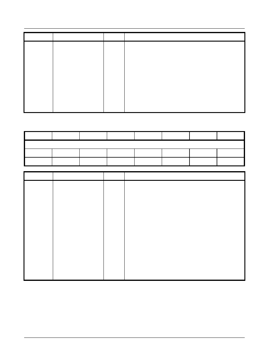
XRT79L71
PRELIMINARY
·Á
·Á
·Á
·Á
REV. P1.0.3
1 - CHANNEL DS3/E3 ATM UNI/PPP COMBO IC
328
0
Filter if Pattern Match
R/W
Filter if Pattern Match - User Cell Filter # 3:This READ/WRITE
bit-field permits the user to either configure User Cell Filter # 3 to
filter (based upon the configuration settings for Bits 1 and 2, in
this register) ATM cells with header bytes that match the "user-
defined" header byte patterns, or to filter ATM cells with header
bytes that do NOT match the "user-defined" header byte pat-
terns.
0 - Configures User Cell Filter # 3 to filter user cells that do NOT
match the header byte patterns (as defined in the " " registers).
1 - Configures User Cell Filter # 3 to filter user cells that do
match the header byte patterns (as defined in the " " registers).
N
OTE
: This bit-field is only active if "User Cell Filter # 3" has
been enabled.
RECEIVE ATM CELL PROCESSOR BLOCK - RECEIVE USER CELL FILTER # 3 - PATTERN REGISTER -
HEADER BYTE 1 (ADDRESS = 0X1774)
B
IT
7
B
IT
6
B
IT
5
B
IT
4
B
IT
3
B
IT
2
B
IT
1
B
IT
0
User Cell Filter # 3 - Pattern Register - Byte 1 [7:0]
R/W
R/W
R/W
R/W
R/W
R/W
R/W
R/W
0
0
0
0
0
0
0
0
B
IT
N
UMBER
N
AME
T
YPE
D
ESCRIPTION
7 - 0
User Cell Filter # 3 - Pat-
tern Register - Header
Byte 1
R/W
User Cell Filter # 3 - Pattern Register - Header Byte 1:
The User Cell filtering criteria (for User Cell Filter # 3) is defined
based upon the contents of 9 read/write registers. These regis-
ters are the four "Receive ATM Cell Processor Block - Receive
User Cell Filter # 3 - Pattern Registers", the four "Receive ATM
Cell Processor Block - Receive User Cell Filter # 3 - Check Reg-
isters" and the "Receive ATM Cell Processor Block - Receive
User Cell Filter # 3 Control Register.
This READ/WRITE register, along with the "Receive ATM Cell
Processor Block - Receive User Cell Filter # 3 - Check Register -
Header Byte 1" permits the user to define the User Cell Filtering
criteria for "Octet # 1" of the incoming User Cell. The user will
write the header byte pattern (for Octet 1) that he/she wishes to
use as part of the "User Cell Filtering" criteria, into this register.
The user will also write in a value into the "Receive ATM Cell
Processor Block - Receive User Cell Filter # 3 - Check Register -
Header Byte 1" that indicates which bits within the first octet of
the incoming cells are to be compared with the contents of this
register.
B
IT
N
UMBER
N
AME
T
YPE
D
ESCRIPTION

·Á
·Á
·Á
·Á
PRELIMINARY
XRT79L71
1 - CHANNEL DS3/E3 ATM UNI/PPP COMBO IC
REV. P1.0.3
329
RECEIVE ATM CELL PROCESSOR BLOCK - RECEIVE USER CELL FILTER # 3 - PATTERN REGISTER -
HEADER BYTE 2 (ADDRESS = 0X1775)
B
IT
7
B
IT
6
B
IT
5
B
IT
4
B
IT
3
B
IT
2
B
IT
1
B
IT
0
User Cell Filter # 3 - Pattern Register - Byte 2 [7:0]
R/W
R/W
R/W
R/W
R/W
R/W
R/W
R/W
0
0
0
0
0
0
0
0
B
IT
N
UMBER
N
AME
T
YPE
D
ESCRIPTION
7 - 0
User Cell Filter # 3 - Pat-
tern Register - Header
Byte 2
R/W
User Cell Filter # 3 - Pattern Register - Header Byte 2:
The User Cell filtering criteria (for User Cell Filter # 3) is defined
based upon the contents of 9 read/write registers. These regis-
ters are the four "Receive ATM Cell Processor Block - Receive
User Cell Filter # 3 - Pattern Registers", the four "Receive ATM
Cell Processor Block - Receive User Cell Filter # 3 - Check Reg-
isters" and the "Receive ATM Cell Processor Block - Receive
User Cell Filter # 3 Control Register.
This READ/WRITE register, along with the "Receive ATM Cell
Processor Block - Receive User Cell Filter # 3 - Check Register -
Header Byte 2" permits the user to define the User Cell Filtering
criteria for "Octet # 2" of the incoming User Cell. The user will
write the header byte pattern (for Octet 2) that he/she wishes to
use as part of the "User Cell Filtering" criteria, into this register.
The user will also write in a value into the "Receive ATM Cell
Processor Block - Receive User Cell Filter # 3 - Check Register -
Header Byte 2" that indicates which bits within the first octet of
the incoming cells are to be compared with the contents of this
register.

XRT79L71
PRELIMINARY
·Á
·Á
·Á
·Á
REV. P1.0.3
1 - CHANNEL DS3/E3 ATM UNI/PPP COMBO IC
330
RECEIVE ATM CELL PROCESSOR BLOCK - RECEIVE USER CELL FILTER # 3 - PATTERN REGISTER -
HEADER BYTE 3 (ADDRESS = 0X1776)
B
IT
7
B
IT
6
B
IT
5
B
IT
4
B
IT
3
B
IT
2
B
IT
1
B
IT
0
User Cell Filter # 3 - Pattern Register - Byte 3 [7:0]
R/W
R/W
R/W
R/W
R/W
R/W
R/W
R/W
0
0
0
0
0
0
0
0
B
IT
N
UMBER
N
AME
T
YPE
D
ESCRIPTION
7 - 0
User Cell Filter # 3 - Pat-
tern Register - Header
Byte 3
R/W
User Cell Filter # 3 - Pattern Register - Header Byte 3:
The User Cell filtering criteria (for User Cell Filter # 3) is defined
based upon the contents of 9 read/write registers. These regis-
ters are the four "Receive ATM Cell Processor Block - Receive
User Cell Filter # 3 - Pattern Registers", the four "Receive ATM
Cell Processor Block - Receive User Cell Filter # 3 - Check Reg-
isters" and the "Receive ATM Cell Processor Block - Receive
User Cell Filter # 3 Control Register.
This READ/WRITE register, along with the "Receive ATM Cell
Processor Block - Receive User Cell Filter # 3 - Check Register -
Header Byte 3" permits the user to define the User Cell Filtering
criteria for "Octet # 3" of the incoming User Cell. The user will
write the header byte pattern (for Octet 3) that he/she wishes to
use as part of the "User Cell Filtering" criteria, into this register.
The user will also write in a value into the "Receive ATM Cell
Processor Block - Receive User Cell Filter # 3 - Check Register -
Header Byte 3" that indicates which bits within the first octet of
the incoming cells are to be compared with the contents of this
register.

·Á
·Á
·Á
·Á
PRELIMINARY
XRT79L71
1 - CHANNEL DS3/E3 ATM UNI/PPP COMBO IC
REV. P1.0.3
331
RECEIVE ATM CELL PROCESSOR BLOCK - RECEIVE USER CELL FILTER # 3 - PATTERN REGISTER -
HEADER BYTE 4 (ADDRESS = 0X1777)
B
IT
7
B
IT
6
B
IT
5
B
IT
4
B
IT
3
B
IT
2
B
IT
1
B
IT
0
User Cell Filter # 3 - Pattern Register - Byte 4 [7:0]
R/W
R/W
R/W
R/W
R/W
R/W
R/W
R/W
0
0
0
0
0
0
0
0
B
IT
N
UMBER
N
AME
T
YPE
D
ESCRIPTION
7 - 0
User Cell Filter # 3 - Pat-
tern Register - Header
Byte 4
R/W
User Cell Filter # 3 - Pattern Register - Header Byte 4:
The User Cell filtering criteria (for User Cell Filter # 3) is defined
based upon the contents of 9 read/write registers. These regis-
ters are the four "Receive ATM Cell Processor Block - Receive
User Cell Filter # 3 - Pattern Registers", the four "Receive ATM
Cell Processor Block - Receive User Cell Filter # 3 - Check Reg-
isters" and the "Receive ATM Cell Processor Block - Receive
User Cell Filter # 3 Control Register.
This READ/WRITE register, along with the "Receive ATM Cell
Processor Block - Receive User Cell Filter # 3 - Check Register -
Header Byte 4" permits the user to define the User Cell Filtering
criteria for "Octet # 4" of the incoming User Cell. The user will
write the header byte pattern (for Octet 4) that he/she wishes to
use as part of the "User Cell Filtering" criteria, into this register.
The user will also write in a value into the "Receive ATM Cell
Processor Block - Receive User Cell Filter # 3 - Check Register -
Header Byte 4" that indicates which bits within the first octet of
the incoming cells are to be compared with the contents of this
register.

XRT79L71
PRELIMINARY
·Á
·Á
·Á
·Á
REV. P1.0.3
1 - CHANNEL DS3/E3 ATM UNI/PPP COMBO IC
332
RECEIVE ATM CELL PROCESSOR BLOCK - RECEIVE USER CELL FILTER # 3 - CHECK REGISTER -
BYTE 1 (ADDRESS = 0X1778)
B
IT
7
B
IT
6
B
IT
5
B
IT
4
B
IT
3
B
IT
2
B
IT
1
B
IT
0
User Cell Filter # 3 - Check Register - Byte 1 [7:0]
R/W
R/W
R/W
R/W
R/W
R/W
R/W
R/W
0
0
0
0
0
0
0
0
B
IT
N
UMBER
N
AME
T
YPE
D
ESCRIPTION
7 - 0
User Cell Filter # 3 -
Check Register - Header
Byte 1
R/W
User Cell Filter # 3 - Check Register - Header Byte 1:
The User Cell filtering criteria (for User Cell Filter # 3) is defined
based upon the contents of 9 read/write registers. These regis-
ters are the four "Receive ATM Cell Processor Block - Receive
User Cell Filter # 3 - Pattern Registers", the four "Receive ATM
Cell Processor Block - Receive User Cell Filter # 3 - Check Reg-
isters" and the "Receive ATM Cell Processor Block - Receive
User Cell Filter # 3 Control Register.
This READ/WRITE register, along with the "Receive ATM Cell
Processor Block - Receive User Cell Filter # 3 - Pattern Register
- Header Byte 1" permits the user to define the User Cell Filter-
ing criteria for "Octet # 1" within the incoming User Cell. More
specifically, these READ/WRITE register bits permit the user to
specify which bit(s) in "Octet 1" of the incoming user cell (in the
Receive ATM Cell Processor Block) are to be checked against
the corresponding bit-fields within the "Receive ATM Cell Pro-
cessor Block - Receive User Cell Filter # 3 - Pattern Register -
Header Byte 1" by the User Cell Filter, when determine whether
to "filter" a given User Cell.
Writing a "1" to a particular bit-field in this register, forces the
User Cell Filter to check and compare the corresponding bit in
"Octet # 1" (of the incoming user cell) with the corresponding bit
in the "Receive ATM Cell Processor Block - Receive User Cell
Filter # 3 - Pattern Register - Header Byte 1".
Writing a "0" to a particular bit-field in this register causes the
User Cell Filter to treat the corresponding bit within "Octet # 1"
(in the incoming user cell) as a "don't care" (e.g., to forgo the
comparison between the corresponding bit in "Octet # 1" of the
incoming user cell with the corresponding bit-field in the
"Receive ATM Cell Processor Block - Receive User Cell Filter # 3
- Pattern Register - Header Byte 1").

·Á
·Á
·Á
·Á
PRELIMINARY
XRT79L71
1 - CHANNEL DS3/E3 ATM UNI/PPP COMBO IC
REV. P1.0.3
333
RECEIVE ATM CELL PROCESSOR BLOCK - RECEIVE USER CELL FILTER # 3 - CHECK REGISTER -
BYTE 2 (ADDRESS = 0X1779)
B
IT
7
B
IT
6
B
IT
5
B
IT
4
B
IT
3
B
IT
2
B
IT
1
B
IT
0
User Cell Filter # 3 - Check Register - Byte 2 [7:0]
R/W
R/W
R/W
R/W
R/W
R/W
R/W
R/W
0
0
0
0
0
0
0
0
B
IT
N
UMBER
N
AME
T
YPE
D
ESCRIPTION
7 - 0
User Cell Filter # 3 -
Check Register - Header
Byte 2
R/W
User Cell Filter # 3 - Check Register - Header Byte 2:
The User Cell filtering criteria (for User Cell Filter # 3) is defined
based upon the contents of 9 read/write registers. These regis-
ters are the four "Receive ATM Cell Processor Block - Receive
User Cell Filter # 3 - Pattern Registers", the four "Receive ATM
Cell Processor Block - Receive User Cell Filter # 3 - Check Reg-
isters" and the "Receive ATM Cell Processor Block - Receive
User Cell Filter # 3 Control Register.
This READ/WRITE register, along with the "Receive ATM Cell
Processor Block - Receive User Cell Filter # 3 - Pattern Register
- Header Byte 2" permits the user to define the User Cell Filter-
ing criteria for "Octet # 2" within the incoming User Cell. More
specifically, these READ/WRITE register bits permit the user to
specify which bit(s) in "Octet 2" of the incoming user cell (in the
Receive ATM Cell Processor Block) are to be checked against
the corresponding bit-fields within the "Receive ATM Cell Pro-
cessor Block - Receive User Cell Filter # 3 - Pattern Register -
Header Byte 2" by the User Cell Filter, when determine whether
to "filter" a given User Cell.
Writing a "1" to a particular bit-field in this register, forces the
User Cell Filter to check and compare the corresponding bit in
"Octet # 2" (of the incoming user cell) with the corresponding bit
in the "Receive ATM Cell Processor Block - Receive User Cell
Filter # 3 - Pattern Register - Header Byte 2".
Writing a "0" to a particular bit-field in this register causes the
User Cell Filter to treat the corresponding bit within "Octet # 2"
(in the incoming user cell) as a "don't care" (e.g., to forgo the
comparison between the corresponding bit in "Octet # 2" of the
incoming user cell with the corresponding bit-field in the
"Receive ATM Cell Processor Block - Receive User Cell Filter # 3
- Pattern Register - Header Byte 2").

XRT79L71
PRELIMINARY
·Á
·Á
·Á
·Á
REV. P1.0.3
1 - CHANNEL DS3/E3 ATM UNI/PPP COMBO IC
334
RECEIVE ATM CELL PROCESSOR BLOCK - RECEIVE USER CELL FILTER # 3 - CHECK REGISTER -
BYTE 3 (ADDRESS = 0X177A)
B
IT
7
B
IT
6
B
IT
5
B
IT
4
B
IT
3
B
IT
2
B
IT
1
B
IT
0
User Cell Filter # 3 - Check Register - Byte 3 [7:0]
R/W
R/W
R/W
R/W
R/W
R/W
R/W
R/W
0
0
0
0
0
0
0
0
B
IT
N
UMBER
N
AME
T
YPE
D
ESCRIPTION
7 - 0
User Cell Filter # 3 -
Check Register - Header
Byte 3
R/W
User Cell Filter # 3 - Check Register - Header Byte 3:
The User Cell filtering criteria (for User Cell Filter # 3) is defined
based upon the contents of 9 read/write registers. These regis-
ters are the four "Receive ATM Cell Processor Block - Receive
User Cell Filter # 3 - Pattern Registers", the four "Receive ATM
Cell Processor Block - Receive User Cell Filter # 3 - Check Reg-
isters" and the "Receive ATM Cell Processor Block - Receive
User Cell Filter # 3 Control Register.
This READ/WRITE register, along with the "Receive ATM Cell
Processor Block - Receive User Cell Filter # 3 - Pattern Register
- Header Byte 3" permits the user to define the User Cell Filter-
ing criteria for "Octet # 3" within the incoming User Cell. More
specifically, these READ/WRITE register bits permit the user to
specify which bit(s) in "Octet 3" of the incoming user cell (in the
Receive ATM Cell Processor Block) are to be checked against
the corresponding bit-fields within the "Receive ATM Cell Pro-
cessor Block - Receive User Cell Filter # 3 - Pattern Register -
Header Byte 3" by the User Cell Filter, when determine whether
to "filter" a given User Cell.
Writing a "1" to a particular bit-field in this register, forces the
User Cell Filter to check and compare the corresponding bit in
"Octet # 3" (of the incoming user cell) with the corresponding bit
in the "Receive ATM Cell Processor Block - Receive User Cell
Filter # 3 - Pattern Register - Header Byte 3".
Writing a "0" to a particular bit-field in this register causes the
User Cell Filter to treat the corresponding bit within "Octet # 3"
(in the incoming user cell) as a "don't care" (e.g., to forgo the
comparison between the corresponding bit in "Octet # 3" of the
incoming user cell with the corresponding bit-field in the
"Receive ATM Cell Processor Block - Receive User Cell Filter # 3
- Pattern Register - Header Byte 3").

·Á
·Á
·Á
·Á
PRELIMINARY
XRT79L71
1 - CHANNEL DS3/E3 ATM UNI/PPP COMBO IC
REV. P1.0.3
335
RECEIVE ATM CELL PROCESSOR BLOCK - RECEIVE USER CELL FILTER # 3 - CHECK REGISTER -
BYTE 4 (ADDRESS = 0X177B)
B
IT
7
B
IT
6
B
IT
5
B
IT
4
B
IT
3
B
IT
2
B
IT
1
B
IT
0
User Cell Filter # 3 - Check Register - Byte 4 [7:0]
R/W
R/W
R/W
R/W
R/W
R/W
R/W
R/W
0
0
0
0
0
0
0
0
B
IT
N
UMBER
N
AME
T
YPE
D
ESCRIPTION
7 - 0
User Cell Filter # 3 -
Check Register - Header
Byte 4
R/W
User Cell Filter # 3 - Check Register - Header Byte 4:
The User Cell filtering criteria (for User Cell Filter # 3) is defined
based upon the contents of 9 read/write registers. These regis-
ters are the four "Receive ATM Cell Processor Block - Receive
User Cell Filter # 3 - Pattern Registers", the four "Receive ATM
Cell Processor Block - Receive User Cell Filter # 3 - Check Reg-
isters" and the "Receive ATM Cell Processor Block - Receive
User Cell Filter # 3 Control Register.
This READ/WRITE register, along with the "Receive ATM Cell
Processor Block - Receive User Cell Filter # 3 - Pattern Register
- Header Byte 4" permits the user to define the User Cell Filter-
ing criteria for "Octet # 4" within the incoming User Cell. More
specifically, these READ/WRITE register bits permit the user to
specify which bit(s) in "Octet 4" of the incoming user cell (in the
Receive ATM Cell Processor Block) are to be checked against
the corresponding bit-fields within the "Receive ATM Cell Pro-
cessor Block - Receive User Cell Filter # 3 - Pattern Register -
Header Byte 4" by the User Cell Filter, when determine whether
to "filter" a given User Cell.
Writing a "1" to a particular bit-field in this register, forces the
User Cell Filter to check and compare the corresponding bit in
"Octet # 4" (of the incoming user cell) with the corresponding bit
in the "Receive ATM Cell Processor Block - Receive User Cell
Filter # 3 - Pattern Register - Header Byte 4".
Writing a "0" to a particular bit-field in this register causes the
User Cell Filter to treat the corresponding bit within "Octet # 4"
(in the incoming user cell) as a "don't care" (e.g., to forgo the
comparison between the corresponding bit in "Octet # 4" of the
incoming user cell with the corresponding bit-field in the
"Receive ATM Cell Processor Block - Receive User Cell Filter # 3
- Pattern Register - Header Byte 4").

XRT79L71
PRELIMINARY
·Á
·Á
·Á
·Á
REV. P1.0.3
1 - CHANNEL DS3/E3 ATM UNI/PPP COMBO IC
336
RECEIVE ATM CELL PROCESSOR BLOCK - RECEIVE USER CELL FILTER # 3 - FILTERED CELL
COUNT - BYTE 3 (ADDRESS = 0X177C)
B
IT
7
B
IT
6
B
IT
5
B
IT
4
B
IT
3
B
IT
2
B
IT
1
B
IT
0
User Cell Filter # 3 - Filtered Cell Count[31:24]
RUR
RUR
RUR
RUR
RUR
RUR
RUR
RUR
0
0
0
0
0
0
0
0
B
IT
N
UMBER
N
AME
T
YPE
D
ESCRIPTION
7 - 0
User Cell Filter # 3 - Fil-
tered Cell Count[31:24]
RUR
User Cell Filter # 3 - Filtered Cell Count[31:24]:
These RESET-upon-READ bit-fields, along with that in the
"Receive ATM Cell Processor Block - Receive User Cell Filter # 3
- Filtered Cell Count - Bytes 2" through "0" register contain a 32-
bit expression for the number of User Cells that have been fil-
tered by User Cell Filter # 3 since the last read of this register.
Depending upon the configuration settings within the "Receive
ATM Cell Processor Block - Receive User Cell Filter Control -
User Cell Filter # 3" Register (Address = 0x1773), these register
bits will be incremented anytime User Cell Filter # 3 performs
any of the following functions.
∑
Discards an incoming "User Cell".
∑
Copies (or Replicates) an incoming "User Cell" and routes the
"copy" to the Receive Cell Extraction Buffer.∑
∑
Both the above actions.
This particular register contains the MSB (Most Significant Byte)
value for this 32-bit expression.
N
OTE
: If the number of "filtered cells" reaches the value
"0xFFFFFFFF" then these registers will saturate to and
remain at this value (e.g., it will not overflow to
"0x00000000").

·Á
·Á
·Á
·Á
PRELIMINARY
XRT79L71
1 - CHANNEL DS3/E3 ATM UNI/PPP COMBO IC
REV. P1.0.3
337
RECEIVE ATM CELL PROCESSOR BLOCK - RECEIVE USER CELL FILTER # 3 - FILTERED CELL
COUNT - BYTE 2 (ADDRESS = 0X177D)
B
IT
7
B
IT
6
B
IT
5
B
IT
4
B
IT
3
B
IT
2
B
IT
1
B
IT
0
User Cell Filter # 3 - Filtered Cell Count[23:16]
RUR
RUR
RUR
RUR
RUR
RUR
RUR
RUR
0
0
0
0
0
0
0
0
B
IT
N
UMBER
N
AME
T
YPE
D
ESCRIPTION
7 - 0
User Cell Filter # 3 - Fil-
tered Cell Count[23:16]
RUR
User Cell Filter # 3 - Filtered Cell Count[23:16]:
These RESET-upon-READ bit-fields, along with that in the
"Receive ATM Cell Processor Block - Receive User Cell Filter # 3
- Filtered Cell Count - Bytes 3, 1 and 0" register contain a 32-bit
expression for the number of User Cells that have been filtered
by User Cell Filter # 3 since the last read of this register.
Depending upon the configuration settings within the "Receive
ATM Cell Processor Block - Receive User Cell Filter Control -
User Cell Filter # 3" Register (Address = 0x1773), these register
bits will be incremented anytime User Cell Filter # 3 performs
any of the following functions.
∑
Discards an incoming "User Cell".
∑
Copies (or Replicates) an incoming "User Cell" and routes the
"copy" to the Receive Cell Extraction Buffer.
∑
Both the above actions.
N
OTE
: If the number of "filtered cells" reaches the value
"0xFFFFFFFF" then these registers will saturate to and
remain at this value (e.g., it will not overflow to
"0x00000000").

XRT79L71
PRELIMINARY
·Á
·Á
·Á
·Á
REV. P1.0.3
1 - CHANNEL DS3/E3 ATM UNI/PPP COMBO IC
338
RECEIVE ATM CELL PROCESSOR BLOCK - RECEIVE USER CELL FILTER # 3 - FILTERED CELL
COUNT - BYTE 1 (ADDRESS = 0X177E)
B
IT
7
B
IT
6
B
IT
5
B
IT
4
B
IT
3
B
IT
2
B
IT
1
B
IT
0
User Cell Filter # 3 - Filtered Cell Count[15:8]
RUR
RUR
RUR
RUR
RUR
RUR
RUR
RUR
0
0
0
0
0
0
0
0
B
IT
N
UMBER
N
AME
T
YPE
D
ESCRIPTION
7 - 0
User Cell Filter # 3 - Fil-
tered Cell Count[15:8]
RUR
User Cell Filter # 3 - Filtered Cell Count[15:8]:
These RESET-upon-READ bit-fields, along with that in the
"Receive ATM Cell Processor Block - Receive User Cell Filter # 3
- Filtered Cell Count - Bytes 3, 2 and 0" register contain a 32-bit
expression for the number of User Cells that have been filtered
by User Cell Filter # 3 since the last read of this register.
Depending upon the configuration settings within the "Receive
ATM Cell Processor Block - Receive User Cell Filter Control -
User Cell Filter # 3" Register (Address = 0x1773), these register
bits will be incremented anytime User Cell Filter # 3 performs
any of the following functions.
∑
Discards an incoming "User Cell".
∑
Copies (or Replicates) an incoming "User Cell" and routes the
"copy" to the Receive Cell Extraction Buffer.
∑
Both the above actions.
N
OTE
: If the number of "filtered cells" reaches the value
"0xFFFFFFFF" then these registers will saturate to and
remain at this value (e.g., it will not overflow to
"0x00000000").

·Á
·Á
·Á
·Á
PRELIMINARY
XRT79L71
1 - CHANNEL DS3/E3 ATM UNI/PPP COMBO IC
REV. P1.0.3
339
RECEIVE ATM CELL PROCESSOR BLOCK - RECEIVE USER CELL FILTER # 3 - FILTERED CELL
COUNT - BYTE 0 (ADDRESS = 0X177F)
B
IT
7
B
IT
6
B
IT
5
B
IT
4
B
IT
3
B
IT
2
B
IT
1
B
IT
0
User Cell Filter # 3 - Filtered Cell Count[7:0]
RUR
RUR
RUR
RUR
RUR
RUR
RUR
RUR
0
0
0
0
0
0
0
0
B
IT
N
UMBER
N
AME
T
YPE
D
ESCRIPTION
7 - 0
User Cell Filter # 3 - Fil-
tered Cell Count[7:0]
RUR
User Cell Filter # 3 - Filtered Cell Count[7:0]:
These RESET-upon-READ bit-fields, along with that in the
"Receive ATM Cell Processor Block - Receive User Cell Filter # 3
- Filtered Cell Count - Bytes 3" through "1" register contain a 32-
bit expression for the number of User Cells that have been fil-
tered by User Cell Filter # 3 since the last read of this register.
Depending upon the configuration settings within the "Receive
ATM Cell Processor Block - Receive User Cell Filter Control -
User Cell Filter # 3" Register (Address = 0x1773), these register
bits will be incremented anytime User Cell Filter # 3 performs
any of the following functions.
∑
Discards an incoming "User Cell".∑
∑
Copies (or Replicates) an incoming "User Cell" and routes the
"copy" to the Receive Cell Extraction Buffer.∑
∑
Both the above actions.
This particular register contains the LSB (Least Significant Byte)
value for this 32-bit expression.
N
OTE
: If the number of "filtered cells" reaches the value
"0xFFFFFFFF" then these registers will saturate to and
remain at this value (e.g., it will not overflow to
"0x00000000").

XRT79L71
PRELIMINARY
·Á
·Á
·Á
·Á
REV. P1.0.3
1 - CHANNEL DS3/E3 ATM UNI/PPP COMBO IC
340
RECEIVE PPP PACKET PROCESSOR BLOCK (PPP APPLICATIONS ONLY)
RECEIVE PPP PACKET PROCESSOR BLOCK - RECEIVE PPP CONTROL REGISTER (ADDRESS =
0X1703)
B
IT
7
B
IT
6
B
IT
5
B
IT
4
B
IT
3
B
IT
2
B
IT
1
B
IT
0
Unused
Receive
CRC-32/
CRC-16*
RxFIFO Over-
flow ABORT
Enable
Unused
De-Scramble
Enable
Delete FCS
from Incoming
Packet
Receive PPP
Packet Pro-
cessor Block
Enable
R/O
R/O
R/W
R/W
R/O
R/W
R/W
R/W
0
0
0
0
0
0
0
0
B
IT
N
UMBER
N
AME
T
YPE
D
ESCRIPTION
7 - 6
Unused
R/O
5
Receive CRC-32/CRC-
16*
R/W
Receive CRC-32/CRC-16* Select:
This READ/WRITE bit-field permits the user to configure the
Receive PPP Packet Processor block to either compute and ver-
ify a CRC-32 or CRC-16 within the incoming PPP packet-stream.
0 - Configures the Receive PPP Packet Processor block to com-
pute and verify a CRC-16 value within each incoming PPP
packet.
1 - Configures the Receive PPP Packet Processor block to com-
pute and verify a CRC-32 value within each incoming PPP
packet.
4
RxFIFO Overflow ABORT
Enable
R/W
3
Unused
R/O
2
Descramble Enable
R/W
1
Delete FCS from Incom-
ing Packet
R/W
0
Receive PPP Packet Pro-
cessor Block Enable
R/W

·Á
·Á
·Á
·Á
PRELIMINARY
XRT79L71
1 - CHANNEL DS3/E3 ATM UNI/PPP COMBO IC
REV. P1.0.3
341
TRANSMIT ATM CELL PROCESSOR BLOCK
This section presents the Register Description/Address Map of the control registers associated with the
Transmit ATM Cell Processor block.
T
ABLE
18: T
RANSMIT
ATM C
ELL
P
ROCESSOR
/PPP P
ACKET
P
ROCESSOR
B
LOCK
- R
EGISTER
/A
DDRESS
M
AP
A
DDRESS
L
OCATION
R
EGISTER
N
AME
T
YPE
D
EFAULT
V
ALUE
T
RANSMIT
ATM C
ELL
P
ROCESSOR
/PPP P
ROCESSOR
B
LOCK
C
ONTROL
R
EGISTERS
0x1F00
Transmit ATM Cell Processor Control Register - Byte 3
R/W
0x00
0x1F01
Transmit ATM Cell Processor Control Register - Byte 2
R/W
0x00
0x1F02
Transmit ATM Cell Processor Control Register - Byte 1
R/W
0x00
0x1F03
Transmit ATM Cell/PPP Processor Control Register - Byte 0
R/W
0x00
0x1F04 - 0x1F06
Reserved
R/O
0x00
0x1F07
Transmit ATM Status Register
R/O
0x00
0x1F05 - 0x1F0A
Reserved
R/O
0x00
0x1F0B
Transmit ATM Cell/PPP Processor Interrupt Status Register
RUR
0x00
0x1F0C - 0x1F0E
Reserved
R/O
0x00
0x1F0F
Transmit ATM Cell/PPP Processor Interrupt Enable Register
R/W
0x00
0x1F10 - 0x1F12
Reserved
R/O
0x00
0x1F13
Transmit ATM Cell Insertion/Extraction Memory Control Register
R/O & R/
W
0x00
0x1F14
Transmit ATM Cell Insertion/Extraction Memory - Byte 3
R/W
0x00
0x1F15
Transmit ATM Cell Insertion/Extraction Memory - Byte 2
R/W
0x00
0x1F16
Transmit ATM Cell Insertion/Extraction Memory - Byte 1
R/W
0x00
0x1F17
Transmit ATM Cell Insertion/Extraction Memory - Byte 0
R/W
0x00
0x1F18
Transmit ATM Cell - Idle Cell Header Byte # 1 Register
R/W
0x00
0x1F19
Transmit ATM Cell - Idle Cell Header Byte # 2 Register
R/W
0x00
0x1F1A
Transmit ATM Cell - Idle Cell Header Byte # 3 Register
R/W
0x00
0x1F1B
Transmit ATM Cell - Idle Cell Header Byte # 4 Register
R/W
0x00
0x1F1C - 0x1F1E
Reserved
R/O
0x00
0x1F1F
Transmit ATM Cell - Idle Cell Payload Byte Register
R/W
0x00
0x1F20
Transmit ATM Cell - Test Cell Header Byte # 1 Register
R/W
0x00
0x1F21
Transmit ATM Cell - Test Cell Header Byte # 2 Register
R/W
0x00
0x1F22
Transmit ATM Cell - Test Cell Header Byte # 3 Register
R/W
0x00
0x1F23
Transmit ATM Cell - Test Cell Header Byte # 4 Register
R/W
0x00
0x1F24 - 0x1F27
Reserved
R/O
0x00
0x1F28
Transmit ATM Cell - Cell Count Register - Byte 3
RUR
0x00

XRT79L71
PRELIMINARY
·Á
·Á
·Á
·Á
REV. P1.0.3
1 - CHANNEL DS3/E3 ATM UNI/PPP COMBO IC
342
0x1F29
Transmit ATM Cell - Cell Count Register - Byte 2
RUR
0x00
0x1F2A
Transmit ATM Cell - Cell Count Register - Byte 1
RUR
0x00
0x1F2B
Transmit ATM Cell - Cell Count Register - Byte 0
RUR
0x00
0x1F2C
Transmit ATM Cell - Discard Cell Count Register - Byte 3
RUR
0x00
0x1F2D
Transmit ATM Cell - Discard Cell Count Register - Byte 2
RUR
0x00
0x1F2E
Transmit ATM Cell - Discard Cell Count Register - Byte 1
RUR
0x00
0x1F2F
Transmit ATM Cell - Discard Cell Count Register - Byte 0
RUR
0x00
0x1F30
Transmit ATM Cell - HEC Byte Error Count Register - Byte 3
RUR
0x00
0x1F31
Transmit ATM Cell - HEC Byte Error Count Register - Byte 2
RUR
0x00
0x1F32
Transmit ATM Cell - HEC Byte Error Count Register - Byte 1
RUR
0x00
0x1F33
Transmit ATM Cell - HEC Byte Error Count Register - Byte 0
RUR
0x00
0x1F34
Transmit ATM Cell - Parity Error Count Register - Byte 3
RUR
0x00
0x1F35
Transmit ATM Cell - Parity Error Count Register - Byte 2
RUR
0x00
0x1F36
Transmit ATM Cell - Parity Error Count Register - Byte 1
RUR
0x00
0x1F37
Transmit ATM Cell - Parity Error Count Register - Byte 0
RUR
0x00
0x1F38 - 0x1F42
Reserved
R/O
0x00
0x1F43
Transmit ATM Controller - Transmit ATM Filter # 0 Control Register
R/W
0x00
0x1F44
Transmit ATM Controller - Transmit ATM Filter # 0 Pattern - Header Byte 1
R/W
0x00
0x1F45
Transmit ATM Controller - Transmit ATM Filter # 0 Pattern - Header Byte 2
R/W
0x00
0x1F46
Transmit ATM Controller - Transmit ATM Filter # 0 Pattern - Header Byte 3
R/W
0x00
0x1F47
Transmit ATM Controller - Transmit ATM Filter # 0 Pattern - Header Byte 4
R/W
0x00
0x1F48
Transmit ATM Controller - Transmit ATM Filter # 0 Check - Header Byte 1
R/W
0x00
0x1F49
Transmit ATM Controller - Transmit ATM Filter # 0 Check - Header Byte 2
R/W
0x00
0x1F4A
Transmit ATM Controller - Transmit ATM Filter # 0 Check - Header Byte 3
R/W
0x00
0x1F4B
Transmit ATM Controller - Transmit ATM Filter # 0 Check - Header Byte 4
R/W
0x00
0x1F4C
Transmit ATM Cell - Cell Count Register - Byte 3
RUR
0x00
0x1F4D
Transmit ATM Cell - Cell Count Register - Byte 2
RUR
0x00
0x1F4E
Transmit ATM Cell - Cell Count Register - Byte 1
RUR
0x00
0x1F4F
Transmit ATM Cell - Cell Count Register - Byte 0
RUR
0x00
0x1F50 - 0x1F52
Reserved
R/O
0x00
0x1F53
Transmit ATM Controller - Transmit ATM Filter # 1 Control Register
R/W
0x00
T
ABLE
18: T
RANSMIT
ATM C
ELL
P
ROCESSOR
/PPP P
ACKET
P
ROCESSOR
B
LOCK
- R
EGISTER
/A
DDRESS
M
AP
A
DDRESS
L
OCATION
R
EGISTER
N
AME
T
YPE
D
EFAULT
V
ALUE
T
RANSMIT
ATM C
ELL
P
ROCESSOR
/PPP P
ROCESSOR
B
LOCK
C
ONTROL
R
EGISTERS

·Á
·Á
·Á
·Á
PRELIMINARY
XRT79L71
1 - CHANNEL DS3/E3 ATM UNI/PPP COMBO IC
REV. P1.0.3
343
0x1F54
Transmit ATM Controller - Transmit ATM Filter # 1 Pattern - Header Byte 1
R/W
0x00
0x1F55
Transmit ATM Controller - Transmit ATM Filter # 1 Pattern - Header Byte 2
R/W
0x00
0x1F56
Transmit ATM Controller - Transmit ATM Filter # 1 Pattern - Header Byte 3
R/W
0x00
0x1F57
Transmit ATM Controller - Transmit ATM Filter # 1 Pattern - Header Byte 4
R/W
0x00
0x1F58
Transmit ATM Controller - Transmit ATM Filter # 1 Check - Header Byte 1
R/W
0x00
0x1F59
Transmit ATM Controller - Transmit ATM Filter # 1 Check - Header Byte 2
R/W
0x00
0x1F5A
Transmit ATM Controller - Transmit ATM Filter # 1 Check - Header Byte 3
R/W
0x00
0x1F5B
Transmit ATM Controller - Transmit ATM Filter # 1 Check - Header Byte 4
R/W
0x00
0x1F5C
Transmit ATM Cell - Cell Count Register - Byte 3
RUR
0x00
0x1F5D
Transmit ATM Cell - Cell Count Register - Byte 2
RUR
0x00
0x1F5E
Transmit ATM Cell - Cell Count Register - Byte 1
RUR
0x00
0x1F5F
Transmit ATM Cell - Cell Count Register - Byte 0
RUR
0x00
0x1F60 - 0x1F62
Reserved
R/O
0x00
0x1F63
Transmit ATM Controller - Transmit ATM Filter # 2 Control Register
R/W
0x00
0x1F64
Transmit ATM Controller - Transmit ATM Filter # 2 Pattern - Header Byte 1
R/W
0x00
0x1F65
Transmit ATM Controller - Transmit ATM Filter # 2 Pattern - Header Byte 2
R/W
0x00
0x1F66
Transmit ATM Controller - Transmit ATM Filter # 2 Pattern - Header Byte 3
R/W
0x00
0x1F67
Transmit ATM Controller - Transmit ATM Filter # 2 Pattern - Header Byte 4
R/W
0x00
0x1F68
Transmit ATM Controller - Transmit ATM Filter # 2 Check - Header Byte 1
R/W
0x00
0x1F69
Transmit ATM Controller - Transmit ATM Filter # 2 Check - Header Byte 2
R/W
0x00
0x1F6A
Transmit ATM Controller - Transmit ATM Filter # 2 Check - Header Byte 3
R/W
0x00
0x1F6B
Transmit ATM Controller - Transmit ATM Filter # 3 Check - Header Byte 4
R/W
0x00
0x1F6C
Transmit ATM Cell - Cell Count Register - Byte 3
RUR
0x00
0x1F6D
Transmit ATM Cell - Cell Count Register - Byte 2
RUR
0x00
0x1F6E
Transmit ATM Cell - Cell Count Register -Byte 1
RUR
0x00
0x1F6F
Transmit ATM Cell - Cell Count Register - Byte 0
RUR
0x00
0x1F70 - 0x1F72
Reserved
R/O
0x00
0x1F73
Transmit ATM Controller - Transmit ATM Filter # 3 Control Register
R/W
0x00
0x1F74
Transmit ATM Controller - Transmit ATM Filter # 3 Pattern - Header Byte 1
R/W
0x00
0x1F75
Transmit ATM Controller - Transmit ATM Filter # 3 Pattern - Header Byte 2
R/W
0x00
0x1F76
Transmit ATM Controller - Transmit ATM Filter # 3 Pattern - Header Byte 3
R/W
0x00
T
ABLE
18: T
RANSMIT
ATM C
ELL
P
ROCESSOR
/PPP P
ACKET
P
ROCESSOR
B
LOCK
- R
EGISTER
/A
DDRESS
M
AP
A
DDRESS
L
OCATION
R
EGISTER
N
AME
T
YPE
D
EFAULT
V
ALUE
T
RANSMIT
ATM C
ELL
P
ROCESSOR
/PPP P
ROCESSOR
B
LOCK
C
ONTROL
R
EGISTERS

XRT79L71
PRELIMINARY
·Á
·Á
·Á
·Á
REV. P1.0.3
1 - CHANNEL DS3/E3 ATM UNI/PPP COMBO IC
344
0x1F77
Transmit ATM Controller - Transmit ATM Filter # 3 Pattern - Header Byte 4
- Channe1 N-1
R/W
0x00
0x1F78
Transmit ATM Controller - Transmit ATM Filter # 3 Check - Header Byte 1
R/W
0x00
0x1F79
Transmit ATM Controller - Transmit ATM Filter # 3 Check - Header Byte 2
R/W
0x00
0x1F7A
Transmit ATM Controller - Transmit ATM Filter # 3 Check - Header Byte 3
R/W
0x00
0x1F7B
Transmit ATM Controller - Transmit ATM Filter # 3 Check - Header Byte 4
R/W
0x00
0x1F7C
Transmit ATM Cell - Cell Count Register - Byte 3
RUR
0x00
0x1F7D
Transmit ATM Cell - Cell Count Register - Byte 2
RUR
0x00
0x1F7E
Transmit ATM Cell - Cell Count Register - Byte 1
RUR
0x00
0x1F7F
Transmit ATM Cell - Cell Count Register - Byte 0
RUR
0x00
0x1F80 - 0x2102
Reserved
R/O
0x00
TRANSMIT ATM CELL PROCESSOR BLOCK - TRANSMIT ATM CONTROL REGISTER - BYTE 2
(ADDRESS = 0X1F01)
B
IT
7
B
IT
6
B
IT
5
B
IT
4
B
IT
3
B
IT
2
B
IT
1
B
IT
0
Unused
Transmit ATM Cell Processor Enable
R/O
R/O
R/O
R/O
R/O
R/O
R/O
R/W
0
0
0
0
0
0
0
0
B
IT
N
UMBER
N
AME
T
YPE
D
ESCRIPTION
7 - 1
Unused
R/O
0
Transmit ATM Cell Pro-
cessor Enable
R/W
Transmit ATM Cell Processor Block Enable:
This READ/WRITE bit-field permits the user to either enable or dis-
able the Transmit ATM Cell Processor block. If the user wishes to
operate a given Channel in the ATM Mode, they must enable the
Transmit ATM Cell Processor Block.
0 - Disables the Transmit ATM Cell Processor Block
1 - Enables the Transmit ATM Cell Processor Bloc
N
OTE
: The user must set this bit-field to "1" before he/she begins to
write ATM cell data into the Transmit UTOPIA Interface
block.
T
ABLE
18: T
RANSMIT
ATM C
ELL
P
ROCESSOR
/PPP P
ACKET
P
ROCESSOR
B
LOCK
- R
EGISTER
/A
DDRESS
M
AP
A
DDRESS
L
OCATION
R
EGISTER
N
AME
T
YPE
D
EFAULT
V
ALUE
T
RANSMIT
ATM C
ELL
P
ROCESSOR
/PPP P
ROCESSOR
B
LOCK
C
ONTROL
R
EGISTERS

·Á
·Á
·Á
·Á
PRELIMINARY
XRT79L71
1 - CHANNEL DS3/E3 ATM UNI/PPP COMBO IC
REV. P1.0.3
345
TRANSMIT ATM CELL PROCESSOR BLOCK - TRANSMIT ATM CONTROL REGISTER - BYTE 1
(ADDRESS = 0X1F02)
B
IT
7
B
IT
6
B
IT
5
B
IT
4
B
IT
3
B
IT
2
B
IT
1
B
IT
0
Test Cell
Transmit
Mode Enable
ONE SHOT
MODE
GFC Inser-
tion Enable -
Bit 3 (MSB)
GFC Inser-
tion Enable -
Bit 2
GFC Inser-
tion Enable -
Bit 1
GFC Inser-
tion Enable -
Bit 0 (LSB)
COSET Poly-
nomial Addi-
tion
Regenerate
HEC Byte
Enable
R/W
R/W
R/W
R/W
R/W
R/W
R/W
R/W
0
0
0
0
0
0
0
0
B
IT
N
UMBER
N
AME
T
YPE
D
ESCRIPTION
7
Test Cell Transmit Mode
Enable
R/W
Test Cell Transmit Mode Enable:
This READ/WRITE bit-field permits the user to enable the Test Cell
Transmitter (within the Transmit ATM Cell Processor Block). The
user must implement this configuration option in order to perform
diagnostic operations with Test Cells.
0 - Disables the Test Cell Transmitter.
1 - Enables the Test Cell Transmitter.
N
OTE
: For normal operation, the user should set this bit-field to "1".
6
One Shot Mode
R/W
One Shot Mode:
If the user has enabled the Test Cell Transmitter, then this READ/
WRITE bit-field permits the user to either configure the Test Cell
Transmitter into the "One-Shot" or in the "Continuous" Mode.
If the user configures the Test Cell Transmitter into the "One-Shot"
Mode, then (whenever the user implements a "0 to 1" transition
within Bit 7 [Test Cell Transmit Mode Enable] of this register) then the
Test Cell Transmitter will generate and transmit 1024 test cells.
Afterwards, the Test Cell Transmitter will halt its transmission of Test
Cells until the user implements another "0 to 1 transition" within Bit 7
(Test Cell Transmit Mode Enable) within this register.
If the user configures the Test Cell Transmitter into the "Continuous"
Mode, then the Test Cell Transmitter will continuously generate and
transmit test cells for the duration that Bit 7(Test Cell Transmit Mode
Enable) is set to "1".
0 - Configures the Test Cell Transmitter to operate in the "Continu-
ous" Mode.
1 - Configures the "Test Cell Transmitter" to operate in the "One-
Shot" Mode.
5
GFC Insertion Enable -
Bit 3
R/W
GFC Insertion Enable - Bit 3 (MSB):
This READ/WRITE bit-field along with GFC Insertion Enable - Bits 2
through 0 permit the user to select the bits (within the GFC nibble of
each "outbound" ATM cell) that will be modified by the contents that
is applied via the "Transmit GFC Serial Input" port, as described
below.
0 - Configures the Transmit GFC Serial Input" port to NOT modify the
contents of Bit 3 (the most significant bit) within the GFC nibble.
1 - Configures the Transmit GFC Serial Input" port to modify the con-
tents of Bit 3 (within the GFC nibble) with the value that is applied via
the Transmit GFC Serial Input Port.

XRT79L71
PRELIMINARY
·Á
·Á
·Á
·Á
REV. P1.0.3
1 - CHANNEL DS3/E3 ATM UNI/PPP COMBO IC
346
4
GFC Insertion Enable -
Bit 2
R/W
GFC Insertion Enable - Bit 2:
This READ/WRITE bit-field along with GFC Insertion Enable - Bits 3,
1 and 0 permit the user to select the bits (within the GFC nibble of
each "outbound" ATM cell) that will be modified by the contents that
is applied via the "Transmit GFC Serial Input" port, as described
below.
0 - Configures the Transmit GFC Serial Input" port to NOT modify the
contents of Bit 2 within the GFC nibble.
1 - Configures the Transmit GFC Serial Input" port to modify the con-
tents of Bit 2 (within the GFC nibble) with the value that is applied via
the Transmit GFC Serial Input Port.
3
GFC Insertion Enable -
Bit 1
R/W
GFC Insertion Enable - Bit 1:
This READ/WRITE bit-field along with GFC Insertion Enable - Bits 3,
2 and 0 permit the user to select the bits (within the GFC nibble of
each "outbound" ATM cell) that will be modified by the contents that
is applied via the "Transmit GFC Serial Input" port, as described
below.
0 - Configures the Transmit GFC Serial Input" port to NOT modify the
contents of Bit 3 (the most significant bit) within the GFC nibble.
1 - Configures the Transmit GFC Serial Input" port to modify the con-
tents of Bit 3 (within the GFC nibble) with the value that is applied via
the Transmit GFC Serial Input Port.
2
GFC Insertion Enable -
Bit 0
R/W
GFC Insertion Enable - Bit 0 (LSB):
This READ/WRITE bit-field along with GFC Insertion Enable - Bits 2
through 0 permit the user to select the bits (within the GFC nibble of
each "outbound" ATM cell) that will be modified by the contents that
is applied via the "Transmit GFC Serial Input" port, as described
below.
0 - Configures the Transmit GFC Serial Input" port to NOT modify the
contents of Bit 0 (the least significant bit) within the GFC nibble.
1 - Configures the Transmit GFC Serial Input" port to modify the con-
tents of Bit 0 (within the GFC nibble) with the value that is applied via
the Transmit GFC Serial Input Port.
1
COSET Polynomial Addi-
tion
R/W
COSET Polynomial Addition:
This READ/WRITE bit-field permits the user to configure the Trans-
mit ATM Cell Processor block to modulo-add the COSET Polynomial
(e.g., x^6 + x^4 + x^2 + 1) to the HEC byte value, within each "out-
bound" ATM cell.
0 - Configures the Transmit ATM Cell Processor block to NOT mod-
ulo-add the COSET Polynomial to the HEC byte within each out-
bound ATM cell.
1 - Configures the Transmit ATM Cell Processor block to modulo-add
the COSET Polynomial to the HEC byte within each outbound ATM
cell.
B
IT
N
UMBER
N
AME
T
YPE
D
ESCRIPTION

·Á
·Á
·Á
·Á
PRELIMINARY
XRT79L71
1 - CHANNEL DS3/E3 ATM UNI/PPP COMBO IC
REV. P1.0.3
347
0
Regenerate HEC Byte
Enable
R/W
Regenerate HEC Byte Enable:
This READ/WRITE bit-field permits the user to configure the Trans-
mit ATM Cell Processor block to automatically re-compute and insert
a new HEC byte into each ATM cell (that it receives from the Trans-
mit UTOPIA Interface block) that contains an uncorrectable HEC
byte.
0 - Does not configure the Transmit ATM Cell Processor block to
compute and insert a new HEC byte into ATM cells that contains an
"uncorrectable" HEC Byte error.
1 - Configures the Transmit ATM Cell Processor block to compute
and insert a new HEC byte into ATM cells that contains an "uncor-
rectable" HEC Byte error.
TRANSMIT ATM CELL PROCESSOR BLOCK - TRANSMIT ATM CONTROL - BYTE 0 (ADDRESS =
0X1F03)
B
IT
7
B
IT
6
B
IT
5
B
IT
4
B
IT
3
B
IT
2
B
IT
1
B
IT
0
HEC Byte
Invert
HEC Byte
Check Enable
Transmit
UTOPIA
Parity Check
Enable
Transmit
UTOPIA
Parity Error -
Discard
Transmit
UTOPIA -
ODD Parity
Reserved
Scrambler
Enable
R/W
R/W
R/W
R/W
R/W
R/O
R/O
R/W
0
0
0
0
0
0
0
0
B
IT
N
UMBER
N
AME
T
YPE
D
ESCRIPTION
7
HEC Byte Invert
R/W
HEC Byte Invert:
This READ/WRITE bit-field permits the user to configure the Trans-
mit ATM Cell Processor block to invert each bit within the newly com-
puted HEC byte of each outbound ATM cell.
0 - Configures the Transmit ATM Cell Processor block to NOT invert
the HEC byte values that it inserts into the fifth octet position within
each outbound ATM cell.
1 - Configures the Transmit ATM Cell Processor block to invert each
bit-field within the newly computed HEC, prior to inserting it into the
fifth octet position, within each outbound ATM cell.
6
HEC Byte Check Enable
R/W
HEC Byte Check Enable:
This READ/WRITE bit-field permits the user to configure the Trans-
mit ATM Cell Processor block to perform HEC byte checking of all
ATM cells that it receives via the Transmit UTOPIA Interface block.
0 - Configures the Transmit ATM Cell Processor block to NOT per-
form HEC byte checking on all ATM cells that it receives via the
Transmit UTOPIA Interface block.
1 - Configures the Transmit ATM Cell Processor block to perform
HEC byte checking on all ATM cells that it receives via the Transmit
UTOPIA Interface block.
B
IT
N
UMBER
N
AME
T
YPE
D
ESCRIPTION

XRT79L71
PRELIMINARY
·Á
·Á
·Á
·Á
REV. P1.0.3
1 - CHANNEL DS3/E3 ATM UNI/PPP COMBO IC
348
5
Transmit UTOPIA Parity
Check Enable
R/W
Transmit UTOPIA Parity Check Enable:
This READ/WRITE bit-field permits the user to either enable or dis-
able "Transmit UTOPIA Interface" Parity checking. If the user
enables "Transmit UTOPIA Interface" Parity Checking, then the
Transmit ATM Cell Processor block will compute either the EVEN or
ODD parity value (depending upon the setting of Bit 3 within this reg-
ister) of each byte or 16-bit word that is input via the Transmit UTO-
PIA Data Bus input pins: (TxUData[15:0]). Afterwards, the Transmit
ATM Cell Processor block will compare this "locally computed" parity
value with that which the ATM Layer Processor has provided to the
"TxUPrty" input pin. If the Transmit ATM Cell Processor detects any
discrepancies between these two parity values (e.g., any parity
errors) then it will take action based upon the user's settings for Bit 4
(Transmit UTOPIA Parity Error - Discard).
0 - Disables "Transmit UTOPIA Interface" Parity Checking.
1 - Enables "Transmit UTOPIA Interface" Parity Checking.
4
Transmit UTOPIA Parity
Error - Discard
R/W
Transmit UTOPIA Parity Error - Discard Cell:
This READ/WRITE bit-field permits the user to configure the Trans-
mit ATM Cell Processor block to either discard or retain (for further
processing) any ATM cell that contains a "Transmit UTOPIA Inter-
face" parity error.
0 - Configures the Transmit ATM Cell Processor block to retain (for
further processing) all cells that contain "Transmit UTOPIA Interface"
parity errors.
1 - Configures the Transmit ATM Cell Processor block to discard all
cells that contain "Transmit UTOPIA Interface" parity errors.
N
OTE
: This bit-field is only valid if "Transmit UTOPIA Interface"
Parity Checking has been enabled.
3
Transmit UTOPIA - Odd
Parity
R/W
Transmit UTOPIA Parity Value - ODD Parity:
This READ/WRITE bit-field permits the user to configure the Trans-
mit ATM Cell Processor block to compute either the EVEN or ODD
parity value for each byte or 16-bit word within each cell that it pro-
cesses. Each of these parity values will ultimately be compared with
the value that is input via the "TxUPrty" input pin (on the Transmit
UTOPIA Interface block) coincident to when ATM cell data is being
applied to the "TxUData[15:0]" input pins.
0 - Configures the Transmit ATM Cell Processor block to compute
and verify the EVEN Parity value of each byte (or 16-bit word) of
ATM cell data that it processes.
1 - Configures the Transmit ATM Cell Processor block to compute
and verify the ODD Parity value of each byte (or 16-bit word) of ATM
cell data that it processes.
N
OTE
: This bit-field is only value if "Transmit UTOPIA Interface"
Parity Checking has been enabled.
2 - 1
Reserved
R/O
B
IT
N
UMBER
N
AME
T
YPE
D
ESCRIPTION

·Á
·Á
·Á
·Á
PRELIMINARY
XRT79L71
1 - CHANNEL DS3/E3 ATM UNI/PPP COMBO IC
REV. P1.0.3
349
0
Scrambler Enable
Cell Payload Scrambler Enable:
This READ/WRITE bit-field permits the user to either enable or dis-
able the "Cell Payload Scrambler". If the user enables the "Cell Pay-
load Scrambler" then the Transmit ATM Cell Processor will payload
self-synchronous scrambling on all cell payloads bytes (within each
outbound ATM cell) with the x^43+1 polynomial.
0 - Disables the Cell Payload Scrambler
1 - Enables the Cell Payload Scrambler
TRANSMIT ATM CELL PROCESSOR BLOCK - TRANSMIT ATM STATUS REGISTER (ADDRESS =
0X1F07)
B
IT
7
B
IT
6
B
IT
5
B
IT
4
B
IT
3
B
IT
2
B
IT
1
B
IT
0
Unused
One Shot DONE
R/O
R/O
R/O
R/O
R/O
R/O
R/O
R/O
0
0
0
0
0
0
0
0
B
IT
N
UMBER
N
AME
T
YPE
D
ESCRIPTION
7 - 1
Unused
R/O
0
One Shot DONE
R/O
One Shot DONE:
This READ-ONLY bit-field indicates whether or not the Test Cell
Transmitter has completed its transmission of 1024 test cells, follow-
ing the instant that the user has commanded the Test Cell to transmit
this burst of 1024 cells.
0 - Indicates that the Test Cell Transmitter has NOT completed its
transmission of 1024 test cells.
1 - Indicates that the Test Cell Transmitter has completed its trans-
mission of 1024 test cells since the last "Transmit Test Cell - One
Shot" command.
N
OTES
:
1.
This bit-field is only valid if (1) the Test Cell Transmitter is
active and (2) if the Test Cell Transmitter has been
configured to operate in the "One-Shot" Mode.
2.
Once this bit-field has been set to "1", it will remain at "1"
until the user executes another "Transmit Test Cell - One
Shot" command.
B
IT
N
UMBER
N
AME
T
YPE
D
ESCRIPTION

XRT79L71
PRELIMINARY
·Á
·Á
·Á
·Á
REV. P1.0.3
1 - CHANNEL DS3/E3 ATM UNI/PPP COMBO IC
350
TRANSMIT ATM CELL PROCESSOR BLOCK - TRANSMIT ATM INTERRUPT STATUS REGISTER
(ADDRESS = 0X1F0B)
B
IT
7
B
IT
6
B
IT
5
B
IT
4
B
IT
3
B
IT
2
B
IT
1
B
IT
0
Unused
Transmit Cell
Extraction
Interrupt Sta-
tus
Transmit Cell
Insertion
Interrupt Sta-
tus
Transmit Cell
Extraction
Memory
Overflow
Interrupt Sta-
tus
Transmit Cell
Insertion
Memory
Overflow
Interrupt Sta-
tus
Detection of
HEC Byte
Error Inter-
rupt Status
Detection of
Transmit
UTOPIA Par-
ity Error Inter-
rupt Status
R/O
R/O
RUR
RUR
RUR
RUR
RUR
RUR
0
0
0
0
0
0
0
0
B
IT
N
UMBER
N
AME
T
YPE
D
ESCRIPTION
7 - 6
Unused
R/O
5
Transmit Cell Extraction
Interrupt Status
RUR
Transmit Cell Extraction Interrupt Status:
This RESET-upon-READ bit-field indicates whether or not the
"Transmit Cell Extraction" interrupt has occurred since the last read
of this register.The Transmit ATM Cell Processor block will generate
the "Transmit Cell Extraction" Interrupt anytime it receives an incom-
ing ATM cell (from the TxFIFO) and loads an ATM cell into the
"Extraction Memory" Buffer.
0 - Indicates that the "Transmit Cell Extraction" Interrupt has NOT
occurred since the last read of this register.
1 - Indicates that the "Transmit Cell Extraction" Interrupt has
occurred since the last read of this register.
4
Transmit Cell Insertion
Interrupt Status
RUR
Transmit Cell Insertion Interrupt:
This RESET-upon-READ bit-field indicates whether or not the
"Transmit Cell Insertion" interrupt has occurred since the last read of
this register.
The Transmit ATM Cell Processor block will generate the "Transmit
Cell Insertion" Interrupt anytime a cell (residing in the Transmit Cell
Insertion Buffer) is read out of the "Transmit Cell Insertion Buffer"
and is loaded into the outbound ATM cell traffic.
0 - Indicates that the "Transmit Cell Insertion" Interrupt has NOT
occurred since the last read of this register.
1 - Indicates that the "Transmit Cell Insertion" Interrupt has occurred
since the last read of this register.
3
Transmit Cell Extraction
Memory Overflow Inter-
rupt Status
RUR
Transmit Cell Extraction Memory Overflow Interrupt Status:
This RESET-upon-READ bit-field indicates whether or not the
"Transmit Cell Extraction Memory Overflow" Interrupt has occurred
since the last read of this register.
The Transmit ATM Cell Processor block will generate this interrupt
anytime an overflow event has occurred in the "Transmit Cell Extrac-
tion Memory" Buffer.
0 - Indicates that the Transmit ATM Cell Processor block has NOT
declared the "Transmit Cell Extraction Memory Overflow" Interrupt
since the last read of this register.
1 - Indicates that the Transmit ATM Cell Processor block has
declared the "Transmit Cell Extraction Memory Overflow" interrupt
since the last read of this register.

·Á
·Á
·Á
·Á
PRELIMINARY
XRT79L71
1 - CHANNEL DS3/E3 ATM UNI/PPP COMBO IC
REV. P1.0.3
351
2
Transmit Cell Insertion
Memory Overflow Inter-
rupt Status
RUR
Transmit Cell Insertion Memory Overflow Interrupt Status:
This RESET-upon-READ bit-field indicates whether or not the Trans-
mit Cell Insertion Memory Overflow" Interrupt has occurred since the
last read of this register.
The Transmit ATM Cell Processor block will generate this interrupt
anytime an overflow event has occurred in the "Transmit Cell Inser-
tion Memory" Buffer.
0 - Indicates that the Transmit ATM Cell Processor block has NOT
declared the "Transmit Cell Insertion Memory Overflow" interrupt
since the last read of this register.
1 - Indicates that the Transmit ATM Cell Processor block has
declared the "Transmit Cell Insertion Memory Overflow" interrupt
since the last read of this register.
1
Detection of HEC Byte
Error Interrupt
RUR
Detection of HEC Byte Error Interrupt:
This RESET-upon-READ bit-field indicates whether or not the
"Transmit ATM Cell Processor block" has declared the "Detection of
HEC Byte Error" Interrupt since the last read of this register.
The Transmit ATM Cell Processor block will generate this interrupt
anytime it has received an ATM cell (from the TxFIFO) that contains
a HEC byte error.
0 - Indicates that the Transmit ATM Cell Processor block has NOT
declared the "Detection of HEC Byte Error" Interrupt since the last
read of this register.
1 - Indicates that the Transmit ATM Cell Processor block has
declared the "Detection of HEC Byte Error" Interrupt since the last
read of this register.
0
Detection of Transmit
UTOPIA Parity Error
Interrupt
Detection of Transmit UTOPIA Parity Error Interrupt:
This RESET-upon-READ bit-field indicates whether or not the
"Transmit ATM Cell Processor" block has declared the "Detection of
Transmit UTOPIA Parity Error" Interrupt since the last read of this
register.
The Transmit ATM Cell Processor block will generate this interrupt
anytime it has received an ATM cell byte or 16-bit word (from the
Transmit UTOPIA Interface block) that contains a parity error.
0 - Indicates that the Transmit ATM Cell Processor block has NOT
declared the "Detection of Transmit UTOPIA Parity Error" Interrupt
since the last read of this register.
1 - Indicates that the Transmit ATM Cell Processor block has
declared the "Detection of Transmit UTOPIA Parity Error" Interrupt
since the last read of this register.
B
IT
N
UMBER
N
AME
T
YPE
D
ESCRIPTION

XRT79L71
PRELIMINARY
·Á
·Á
·Á
·Á
REV. P1.0.3
1 - CHANNEL DS3/E3 ATM UNI/PPP COMBO IC
352
TRANSMIT ATM CELL PROCESSOR BLOCK - TRANSMIT ATM INTERRUPT ENABLE REGISTER
(ADDRESS = 0X1F0F)
B
IT
7
B
IT
6
B
IT
5
B
IT
4
B
IT
3
B
IT
2
B
IT
1
B
IT
0
Unused
Transmit Cell
Extraction
Interrupt
Enable
Transmit Cell
Insertion
Interrupt
Enable
Transmit Cell
Extraction
Memory
Overflow
Interrupt
Enable
Transmit Cell
Insertion
Memory
Overflow
Interrupt
Enable
Detection of
HEC Byte
Error Inter-
rupt Enable
Detection of
Transmit
UTOPIA Par-
ity Error Inter-
rupt Enable
R/O
R/O
R/W
R/W
R/W
R/W
R/W
R/W
0
0
0
0
0
0
0
0
B
IT
N
UMBER
N
AME
T
YPE
D
ESCRIPTION
7 - 6
Unused
5
Transmit Cell Extraction
Interrupt Enable
R/W
Transmit Cell Extraction Interrupt Enable:
This READ/WRITE bit-field permits the user to either enable or dis-
able the "Transmit Cell Extraction" Interrupt.
If the user enables this feature, then the Transmit ATM Cell Proces-
sor block will generate the "Transmit Cell Extraction" Interrupt any-
time it receives an incoming ATM cell (from the TxFIFO) and loads
this ATM cell into the "Transmit Extraction Memory" Buffer.
0 - Disables the "Transmit Cell Extraction" Interrupt.
1 - Enables the "Transmit Cell Extraction" Interrupt
4
Transmit Cell Insertion
Interrupt Enable
R/W
Transmit Cell Insertion Interrupt Enable:
This READ/WRITE bit-field permits the user to either enable or dis-
able the "Transmit Cell Insertion" Interrupt.
If the user enables this feature, then the Transmit ATM Cell Proces-
sor block will generate the "Transmit Cell Insertion" Interrupt anytime
a cell (residing in the "Transmit Cell Insertion" Buffer) is read out of
the "Transmit Cell Insertion" Buffer and is loaded into the "outbound"
ATM cell traffic.
0 - Disables the Transmit Cell Insertion Interrupt.
1 - Enables the Transmit Cell Insertion Interrupt.
3
Transmit Cell Extraction
Memory Overflow Inter-
rupt Enable
R/W
Transmit Cell Extraction Memory Overflow Interrupt Enable:
This READ/WRITE bit-field permits the user to either enable or dis-
able the "Transmit Cell Extraction Memory Overflow" Interrupt.
If the user enables this interrupt, then the Transmit ATM Cell Proces-
sor block will generate an interrupt any time an overflow event has
occurred in the "Transmit Cell Extraction Memory" buffer.
0 - Disables the Transmit Cell Extraction Memory Overflow Interrupt.
1 - Enables the Transmit Cell Extraction Memory Overflow Interrupt.

·Á
·Á
·Á
·Á
PRELIMINARY
XRT79L71
1 - CHANNEL DS3/E3 ATM UNI/PPP COMBO IC
REV. P1.0.3
353
2
Transmit Cell Insertion
Memory Overflow Inter-
rupt Enable
R/W
Transmit Cell Insertion Memory Overflow Interrupt Enable:
This READ/WRITE bit-field permits the user to either enable or dis-
able the "Transmit Cell Insertion Memory Overflow" Interrupt.
If the user enables this interrupt, then the Transmit ATM Cell Proces-
sor block will generate an interrupt any time an overflow event has
occurred in the "Transmit Cell Insertion Memory" buffer.
0 - Disables the Transmit Cell Insertion Memory Overflow Interrupt.
1 - Enables the Transmit Cell Insertion Memory Overflow Interrupt.
1
Detection of HEC Byte
Error Interrupt Enable
R/W
Detection of HEC Byte Error Interrupt Enable:
This READ/WRITE bit-field permits the user to either enable or dis-
able the "Detection of HEC Byte Error Interrupt" within the Transmit
ATM Cell Processor Block.
If the user enables this interrupt, then the Transmit ATM Cell Proces-
sor block will generate an interrupt each time it receives an ATM cell
(from the TxFIFO) that contains a HEC Byte error.
0 - Disables the "Detection of HEC Byte Error" Interrupt.
1 - Enables the "Detection of HEC Byte Error" Interrupt
0
Detection of Transmit
UTOPIA Parity Error
Interrupt Enable
Detection of Transmit UTOPIA Parity Error Interrupt Enable:
This READ/WRITE bit-field permits the user to either enable or dis-
able the "Detection of Transmit UTOPIA Parity Error" Interrupt within
the Transmit ATM Cell Processor block.
If the user enables this interrupt, then the Transmit ATM Cell Proces-
sor block will generate an interrupt each time it receives an ATM cell
byte or 16-bit word (from the TxFIFO) that contains a parity error.
0 - Disables the "Detection of Transmit UTOPIA Parity Error" Inter-
rupt.
1 - Enables the "Detection of Transmit UTOPIA Parity Error" Inter-
rupt.
B
IT
N
UMBER
N
AME
T
YPE
D
ESCRIPTION

XRT79L71
PRELIMINARY
·Á
·Á
·Á
·Á
REV. P1.0.3
1 - CHANNEL DS3/E3 ATM UNI/PPP COMBO IC
354
TRANSMIT ATM CELL PROCESSOR BLOCK - TRANSMIT ATM CELL INSERTION/EXTRACTION
MEMORY CONTROL REGISTER (0X1F13)
B
IT
7
B
IT
6
B
IT
5
B
IT
4
B
IT
3
B
IT
2
B
IT
1
B
IT
0
Unused
Transmit Cell
Extraction
Memory
RESET*
Transmit Cell
Extraction
Memory
CLAV
Transmit Cell
Insertion
Memory
RESET*
Transmit Cell
Insertion
Memory
ROOM
Transmit Cell
Insertion
Memory
WSOC
R/O
R/O
R/O
R/W
R/O
R/W
R/O
W/O
0
0
0
1
0
1
0
0
B
IT
N
UMBER
N
AME
T
YPE
D
ESCRIPTION
7-5
Unused
4
Transmit Cell Extraction
Memory RESET*
R/W
Transmit Cell Extraction Memory RESET*:
This READ/WRITE bit-field permits the user to perform a REST
operation to the Transmit Cell Extraction Memory.
If the user writes a "1-to-0 transition" into this bit-field, then the fol-
lowing events will occur.
a. All of the contents of the Transmit Cell Extraction Memory will
be flushed.
b. All READ and WRITE pointers will be reset to their default
positions.
N
OTE
: Following this RESET event, the user must write the value "1"
into this bit-field in order to enable normal operation within
the Transmit Cell Extraction Memory.
3
Transmit Cell Extraction
Memory CLAV
R/O
Transmit Cell Extraction Memory - Cell Available Indicator:
This READ-ONLY bit-field indicates whether or not there is at least
ATM cell of data (residing within the Transmit Cell Extraction Mem-
ory) that needs to be read out via the Microprocessor Interface.
0 - Indicates that the Transmit Cell Extraction Memory is empty and
contains no ATM cell data.
1 - Indicates that the Transmit Cell Extraction Memory contains at
least one ATM cell of data that needs to be read out.
N
OTE
: The user should validate each ATM cell that is being read out
from the Transmit Cell Extraction memory by checking the
state of this bit-field prior to reading out the contents of ATM
cell data residing within the Transmit Cell Extraction Memory
2
Transmit Cell Insertion
Memory RESET*
R/W
Transmit Cell Insertion Memory RESET*:
This READ/WRITE bit-field permits the user to perform a RESET
operation to the Transmit Cell Insertion Memory.
If the user writes a "1-to-0 transition" into this bit-field, then the fol-
lowing events will occur.
a. All of the contents of the Transmit Cell Insertion Memory will
be flushed.
b. All READ and WRITE pointers will be reset to their default
positions.
N
OTE
: Following this RESET event, the user must write the value "1"
into this bit-field in order to enable normal operation of the
Transmit Cell Insertion Memory.

·Á
·Á
·Á
·Á
PRELIMINARY
XRT79L71
1 - CHANNEL DS3/E3 ATM UNI/PPP COMBO IC
REV. P1.0.3
355
1
Transmit Cell Insertion
Memory ROOM
R/O
Transmit Cell Insertion Memory - ROOM Indicator:
This READ-ONLY bit-field indicates whether or not there is room
(e.g., empty space) available for the contents of another ATM cell to
be written into the Transmit Cell Insertion Memory.
0 - Indicates that the Transmit Cell Insertion Memory does not con-
tain enough empty space to receive another ATM cell via the Micro-
processor Interface.
1 - Indicates that the Transmit Cell Insertion Memory does contain
enough empty space to receive another ATM cell via the Micropro-
cessor Interface.
N
OTE
: The user should verify that the Transmit Cell Insertion
Memory has sufficient empty space to accept another ATM
cell of data (via the Microprocessor Interface) by polling the
state of this bit-field prior to writing each cell into the
Transmit Cell Insertion Memory.
0
Transmit Cell Insertion
Memory WSOC
W/O
Transmit Cell Insertion Memory - Write SOC (Start of Cell):
Whenever the user is writing the contents of an ATM cell into the
Transmit Cell Insertion Memory, then he/she is suppose to identify/
designate the very first byte of this ATM cell by setting this bit-field to
"1".
When the user does this, then the Transmit Cell Insertion Memory
will "know" that the next octet that is written into the "Transmit ATM
Cell Processor Block - Transmit Cell Insertion/Extraction Memory
Data Register - Byte 3 (Address = 0x1F14) is designated as the first
byte of the ATM cell currently being written into the Transmit Cell
Insertion Memory.
N
OTE
: This bit-field must be set to "0" during all other WRITE
operations to the Transmit ATM Cell Processor - Transmit
Cell Insertion/Extraction Memory Data Register
B
IT
N
UMBER
N
AME
T
YPE
D
ESCRIPTION
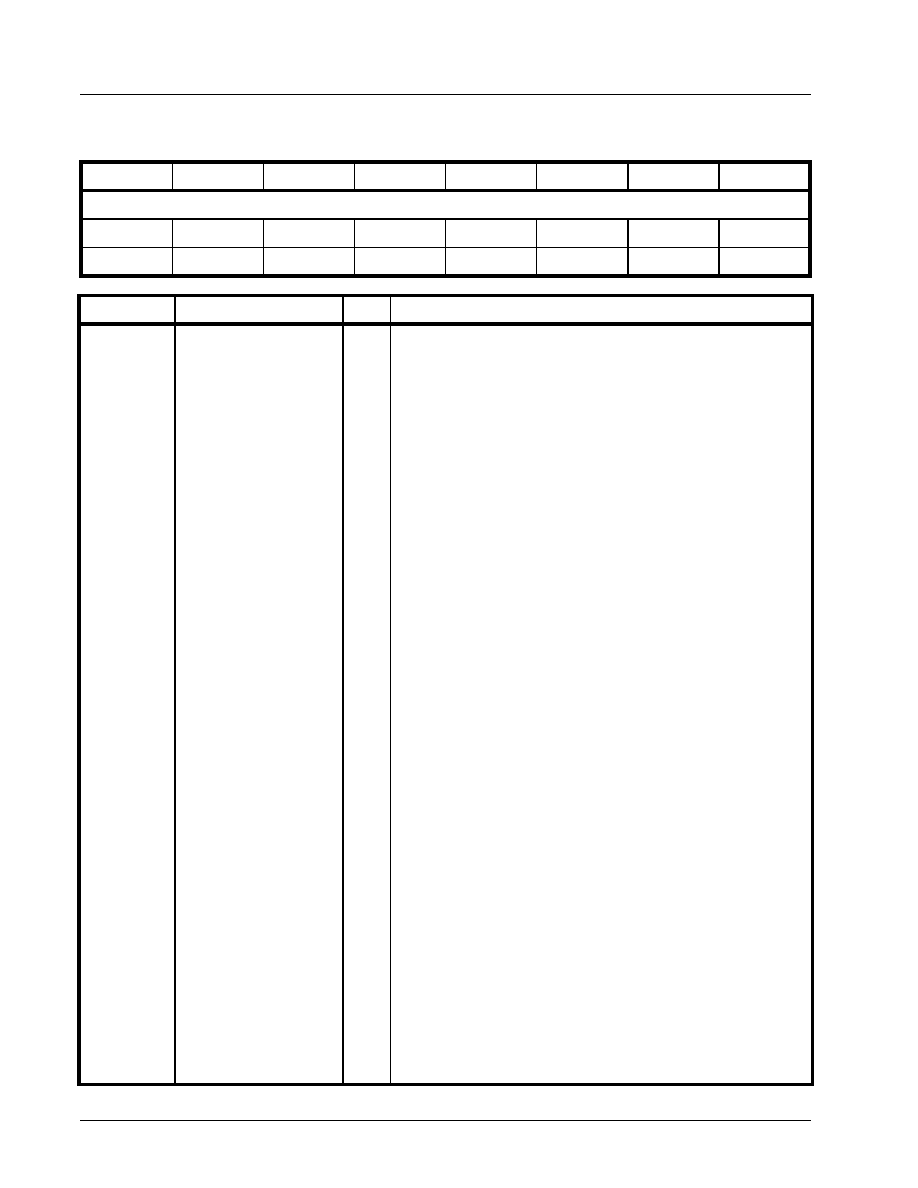
XRT79L71
PRELIMINARY
·Á
·Á
·Á
·Á
REV. P1.0.3
1 - CHANNEL DS3/E3 ATM UNI/PPP COMBO IC
356
TRANSMIT ATM CELL PROCESSOR BLOCK - TRANSMIT CELL INSERTION/EXTRACTION MEMORY
DATA - BYTE 3 (ADDRESS = 0X1F14)
B
IT
7
B
IT
6
B
IT
5
B
IT
4
B
IT
3
B
IT
2
B
IT
1
B
IT
0
Transmit Cell Insertion/Extraction Memory Data[31:24]
R/W
R/W
R/W
R/W
R/W
R/W
R/W
R/W
0
0
0
0
0
0
0
0
B
IT
N
UMBER
N
AME
T
YPE
D
ESCRIPTION
7 - 0
Transmit Cell Insertion/
Extraction Memory
Data[31:24]
R/W
Transmit Cell Insertion/Extraction Memory Data[31:24]:
These READ/WRITE bit-fields, along with that in the "Transmit ATM
Cell Processor Block - Transmit Cell Insertion/Extraction Memory
Data - Bytes 2 through 0" support the following functions.
a. They function as the address location for the user to write the
contents of an "outbound" ATM cell into the Transmit Cell
Insertion Memory, via the Microprocessor Interface.
b. They function as the address location, for which the user to
read out the contents of an "inbound" ATM cell from the
Receive Cell Extraction Memory, via the Microprocessor
Interface.
N
OTES
:
1.
If the user performs a WRITE operation to this (and the
other three address locations), then he/she is writing ATM
cell data into the Transmit Cell Insertion Memory.
2.
If the user performs a READ operation to this (and the other
three address locations), then he/she is reading ATM cell
data from the Transmit Cell Extraction Memory.
3.
READ and WRITE operations must be performed in a "32-
bit" (4-byte "word") manner. Hence, whenever the user
performs a READ/WRITE operation to these address
locations, he/she must start by writing in or reading out the
first byte (of this "4-byte" word) of a given ATM cell, into/
from this particular address location. Next, the user must
perform the READ/WRITE operation (with the second of
this "4-byte" word) to the "Transmit ATM Cell Processor
Block - Transmit Cell Insertion/Extraction Memory - Byte 2
register. Afterwards, the user must perform a READ/
WRITE operation (with the third of this "4-byte" word) to the
Transmit ATM Cell Processor Block - Transmit Cell
Insertion/Extraction Memory - Byte 1 register. Finally, the
user must perform a READ/WRITE operation (with the
fourth of this "4-byte" word) to the Transmit ATM Cell
Processor Block - Transmit Cell Insertion/Extraction
Memory - Byte 0 register. When reading out (writing in) the
next four bytes of a given ATM Cell, the user must repeat
this process with a READ or WRITE operation, from/to this
register location, and so on.
4.
Whenever the user is writing cell data into the Transmit Cell
Insertion Memory, the size of the Cell is always 56 bytes.
5.
Whenever the user is reading cell data from the Transmit
Cell Extraction Memory, the size of the Cell is always 56
bytes.

·Á
·Á
·Á
·Á
PRELIMINARY
XRT79L71
1 - CHANNEL DS3/E3 ATM UNI/PPP COMBO IC
REV. P1.0.3
357
TRANSMIT ATM CELL PROCESSOR BLOCK - TRANSMIT CELL INSERTION/EXTRACTION MEMORY
DATA - BYTE 2 (ADDRESS = 0X1F15)
B
IT
7
B
IT
6
B
IT
5
B
IT
4
B
IT
3
B
IT
2
B
IT
1
B
IT
0
Transmit Cell Insertion/Extraction Memory Data[23:16]
R/W
R/W
R/W
R/W
R/W
R/W
R/W
R/W
0
0
0
0
0
0
0
0
B
IT
N
UMBER
N
AME
T
YPE
D
ESCRIPTION
7 - 0
Transmit Cell Insertion/
Extraction Memory
Data[23:16]
R/W
Transmit Cell Insertion/Extraction Memory Data[23:16]:
These READ/WRITE bit-fields, along with that in the "Transmit ATM
Cell Processor Block - Transmit Cell Insertion/Extraction Memory Data
- Bytes 3, 1 and 0" support the following functions.
a. They function as the address location for the user to write the
contents of an "outbound" ATM cell into the Transmit Cell
Insertion Memory, via the Microprocessor Interface.
b. They function as the address location, for which the user to read
out the contents of an "inbound" ATM cell from the Receive Cell
Extraction Memory, via the Microprocessor Interface.
N
OTES
:
1.
If the user performs a WRITE operation to this (and the other
three address locations), then he/she is writing ATM cell data
into the Transmit Cell Insertion Memory.
2.
If the user performs a READ operation to this (and the other
three address locations), then he/she is reading ATM cell
data from the Transmit Cell Extraction Memory.
3.
READ and WRITE operations must be performed in a "32-
bit" (4-byte "word") manner. Hence, whenever the user
performs a READ/WRITE operation to these address
locations, he/she must start by writing in or reading out the
first byte (of this "4-byte" word) of a given ATM cell, into/from
the Transmit ATM Cell Processor Block - Transmit Cell
Insertion/Extraction Memory - Byte 3" register. Next, the
user must perform the READ/WRITE operation (with the
second of this "4-byte" word) to this particular address
location. Afterwards, the user must perform a READ/WRITE
operation (with the third of this "4-byte" word) to the Transmit
ATM Cell Processor Block - Transmit Cell Insertion/Extraction
Memory - Byte 1 register. Finally, the user must perform a
READ/WRITE operation (with the fourth of this "4-byte" word)
to the Transmit ATM Cell Processor Block - Transmit Cell
Insertion/Extraction Memory - Byte 0 register. When reading
out (writing in) the next four bytes of a given ATM Cell, the
user must repeat this process with a READ or WRITE
operation, from/to this register location, and so on.
4.
Whenever the user is writing cell data into the Transmit Cell
Insertion Memory, the size of the Cell is always 56 bytes.
5.
Whenever the user is reading cell data from the Transmit Cell
Extraction Memory, the size of the Cell is always 56 bytes.

XRT79L71
PRELIMINARY
·Á
·Á
·Á
·Á
REV. P1.0.3
1 - CHANNEL DS3/E3 ATM UNI/PPP COMBO IC
358
TRANSMIT ATM CELL PROCESSOR BLOCK - TRANSMIT CELL INSERTION/EXTRACTION MEMORY
DATA - BYTE 1 (ADDRESS = 0X1F16)
B
IT
7
B
IT
6
B
IT
5
B
IT
4
B
IT
3
B
IT
2
B
IT
1
B
IT
0
Transmit Cell Insertion/Extraction Memory Data[15:8]
R/W
R/W
R/W
R/W
R/W
R/W
R/W
R/W
0
0
0
0
0
0
0
0
B
IT
N
UMBER
N
AME
T
YPE
D
ESCRIPTION
7 - 0
Transmit Cell Insertion/
Extraction Memory
Data[15:8]
R/W
Transmit Cell Insertion/Extraction Memory Data[15:8]:
These READ/WRITE bit-fields, along with that in the "Transmit ATM
Cell Processor Block - Transmit Cell Insertion/Extraction Memory Data
- Bytes 3, 2 and 0" support the following functions.
a. Transmit Cell Insertion/Extraction Memory Data[15:8]:These
READ/WRITE bit-fields, along with that in the "Transmit ATM
Cell Processor Block - Transmit Cell Insertion/Extraction
Memory Data - Bytes 3, 2 and 0" support the following
functions.a.They function as the address location for the user to
write the contents of an "outbound" ATM cell into the Transmit
Cell Insertion Memory, via the Microprocessor Interface.
b. They function as the address location, for which the user to read
out the contents of an "inbound" ATM cell from the Receive Cell
Extraction Memory, via the Microprocessor Interface.
N
OTES
:
1.
If the user performs a WRITE operation to this (and the other
three address locations), then he/she is writing ATM cell data
into the Transmit Cell Insertion Memory.
2.
If the user performs a READ operation to this (and the other
three address locations), then he/she is reading ATM cell
data from the Transmit Cell Extraction Memory.
3.
READ and WRITE operations must be performed in a "32-
bit" (4-byte "word") manner. Hence, whenever the user
performs a READ/WRITE operation to these address
locations, he/she must start by writing in or reading out the
first byte (of this "4-byte" word) of a given ATM cell, into/from
the Transmit ATM Cell Processor Block - Transmit Cell
Insertion/Extraction Memory - Byte 3 register. Next, the user
must perform the READ/WRITE operation (with the second
of this "4-byte" word) to the "Transmit ATM Cell Processor
Block - Transmit Cell Insertion/Extraction Memory - Byte 2
register. Afterwards, the user must perform a READ/WRITE
operation (with the third of this "4-byte" word) to this
particular register location. Finally, the user must perform a
READ/WRITE operation (with the fourth of this "4-byte" word)
to the Transmit ATM Cell Processor Block - Transmit Cell
Insertion/Extraction Memory - Byte 0 register. When reading
out (writing in) the next four bytes of a given ATM Cell, the
user must repeat this process with a READ or WRITE
operation, from/to this register location, and so on.
4.
Whenever the user is writing cell data into the Transmit Cell
Insertion Memory, the size of the Cell is always 56 bytes.
5.
Whenever the user is reading cell data from the Transmit Cell
Extraction Memory, the size of the Cell is always 56 bytes.

·Á
·Á
·Á
·Á
PRELIMINARY
XRT79L71
1 - CHANNEL DS3/E3 ATM UNI/PPP COMBO IC
REV. P1.0.3
359
TRANSMIT ATM CELL PROCESSOR BLOCK - TRANSMIT CELL INSERTION/EXTRACTION MEMORY
DATA - BYTE 0 (ADDRESS = 0X1F17)
B
IT
7
B
IT
6
B
IT
5
B
IT
4
B
IT
3
B
IT
2
B
IT
1
B
IT
0
Transmit Cell Insertion/Extraction Memory Data[7:0]
R/W
R/W
R/W
R/W
R/W
R/W
R/W
R/W
0
0
0
0
0
0
0
0
B
IT
N
UMBER
N
AME
T
YPE
D
ESCRIPTION
7 - 0
Transmit Cell Insertion/
Extraction Memory
Data[7:0]
R/W
Transmit Cell Insertion/Extraction Memory Data[7:0]:
These READ/WRITE bit-fields, along with that in the "Transmit ATM
Cell Processor Block - Transmit Cell Insertion/Extraction Memory Data
- Bytes 3, through 1" support the following functions.
a. They function as the address location for the user to write the
contents of an "outbound" ATM cell into the Transmit Cell
Insertion Memory, via the Microprocessor Interface.
b. They function as the address location, for which the user to read
out the contents of an "inbound" ATM cell from the Receive Cell
Extraction Memory, via the Microprocessor Interface.
N
OTES
:
1.
If the user performs a WRITE operation to this (and the other
three address locations), then he/she is writing ATM cell data
into the Transmit Cell Insertion Memory.
2.
If the user performs a READ operation to this (and the other
three address locations), then he/she is reading ATM cell
data from the Transmit Cell Extraction Memory.
3.
READ and WRITE operations must be performed in a "32-
bit" (4-byte "word") manner. Hence, whenever the user
performs a READ/WRITE operation to these address
locations, he/she must start by writing in or reading out the
first byte (of this "4-byte" word) of a given ATM cell, into/from
the Transmit ATM Cell Processor Block - Transmit Cell
Insertion/Extraction Memory - Byte 3 register. Next, the user
must perform the READ/WRITE operation (with the second
of this "4-byte" word) to the "Transmit ATM Cell Processor
Block - Transmit Cell Insertion/Extraction Memory - Byte 2
register. Afterwards, the user must perform a READ/WRITE
operation (with the third of this "4-byte" word) to the "Transmit
ATM Cell Processor Block - Transmit Cell Insertion/Extraction
Memory - Byte 1" register. Finally, the user must perform a
READ/WRITE operation (with the fourth of this "4-byte" word)
to this particular register location. When reading out (writing
in) the next four bytes of a given ATM Cell, the user must
repeat this process with a READ or WRITE operation, from/
to this register location, and so on.
4.
Whenever the user is writing cell data into the Transmit Cell
Insertion Memory, the size of the Cell is always 56 bytes.
5.
Whenever the user is reading cell data from the Transmit Cell
Extraction Memory, the size of the Cell is always 56 bytes.

XRT79L71
PRELIMINARY
·Á
·Á
·Á
·Á
REV. P1.0.3
1 - CHANNEL DS3/E3 ATM UNI/PPP COMBO IC
360
TRANSMIT ATM CELL PROCESSOR BLOCK - TRANSMIT ATM IDLE CELL HEADER BYTE 1 (ADDRESS
= 0X1F18)
B
IT
7
B
IT
6
B
IT
5
B
IT
4
B
IT
3
B
IT
2
B
IT
1
B
IT
0
Transmit Idle Cell Header Byte 1 [7:0]
R/W
R/W
R/W
R/W
R/W
R/W
R/W
R/W
0
0
0
0
0
0
0
0
B
IT
N
UMBER
N
AME
T
YPE
D
ESCRIPTION
7 - 0
Transmit Idle Cell
Header Byte - 1 [7:0]
R/W
Transmit Idle Cell Header Byte - 1[7:0]:
These READ/WRITE register bits, along with that in "Transmit ATM
Cell Processor Block - Transmit ATM Idle Cell Header Byte 2 through
Byte 4" registers permit the user to define the header byte pattern of
all Idle Cells that are generated by the Transmit ATM Cell Processor
block.
This register permits the user to define/specify the value of Header
Byte # 1 within each Idle Cell that is generated and transmitted by the
Transmit ATM Cell Processor block.
TRANSMIT ATM CELL PROCESSOR BLOCK - TRANSMIT ATM IDLE CELL HEADER BYTE 2 (ADDRESS
= 0X1F19)
B
IT
7
B
IT
6
B
IT
5
B
IT
4
B
IT
3
B
IT
2
B
IT
1
B
IT
0
Transmit Idle Cell Header Byte 2 [7:0]
R/W
R/W
R/W
R/W
R/W
R/W
R/W
R/W
0
0
0
0
0
0
0
0
B
IT
N
UMBER
N
AME
T
YPE
D
ESCRIPTION
7 - 0
Transmit Idle Cell
Header Byte - 2 [7:0]
R/W
Transmit Idle Cell Header Byte - 2[7:0]:
These READ/WRITE register bits, along with that in "Transmit ATM
Cell Processor Block - Transmit ATM Idle Cell Header Bytes 1, 3 and
4" registers permit the user to define the header byte pattern of all Idle
Cells that are generated by the Transmit ATM Cell Processor block.
This register permits the user to define/specify the value of Header
Byte # 2 within each Idle Cell that is generated and transmitted by the
Transmit ATM Cell Processor block.

·Á
·Á
·Á
·Á
PRELIMINARY
XRT79L71
1 - CHANNEL DS3/E3 ATM UNI/PPP COMBO IC
REV. P1.0.3
361
TRANSMIT ATM CELL PROCESSOR BLOCK - TRANSMIT ATM IDLE CELL HEADER BYTE 3 (ADDRESS
= 0X1F1A)
B
IT
7
B
IT
6
B
IT
5
B
IT
4
B
IT
3
B
IT
2
B
IT
1
B
IT
0
Transmit Idle Cell Header Byte 3 [7:0]
R/W
R/W
R/W
R/W
R/W
R/W
R/W
R/W
0
0
0
0
0
0
0
0
B
IT
N
UMBER
N
AME
T
YPE
D
ESCRIPTION
7 - 0
Transmit Idle Cell
Header Byte - 3 [7:0]
R/W
Transmit Idle Cell Header Byte - 3[7:0]:
These READ/WRITE register bits, along with that in "Transmit ATM
Cell Processor Block - Transmit ATM Idle Cell Header Bytes 1, 2 and
4" registers permit the user to define the header byte pattern of all Idle
Cells that are generated by the Transmit ATM Cell Processor block.
This register permits the user to define/specify the value of Header
Byte # 3 within each Idle Cell that is generated and transmitted by the
Transmit ATM Cell Processor block.
TRANSMIT ATM CELL PROCESSOR BLOCK - TRANSMIT ATM IDLE CELL HEADER BYTE 4 (ADDRESS
= 0X1F1B)
B
IT
7
B
IT
6
B
IT
5
B
IT
4
B
IT
3
B
IT
2
B
IT
1
B
IT
0
Transmit Idle Cell Header Byte 4 [7:0]
R/W
R/W
R/W
R/W
R/W
R/W
R/W
R/W
0
0
0
0
0
0
0
0
B
IT
N
UMBER
N
AME
T
YPE
D
ESCRIPTION
7 - 0
Transmit Idle Cell
Header Byte - 4 [7:0]
R/W
Transmit Idle Cell Header Byte - 4[7:0]:
These READ/WRITE register bits, along with that in "Transmit ATM
Cell Processor Block - Transmit ATM Idle Cell Header Byte 1 through
Byte 3" registers permit the user to define the header byte pattern of
all Idle Cells that are generated by the Transmit ATM Cell Processor
block.
This register permits the user to define/specify the value of Header
Byte # 4 within each Idle Cell that is generated and transmitted by the
Transmit ATM Cell Processor block.
XRT79L71
PRELIMINARY
·Á
·Á
·Á
·Á
REV. P1.0.3
1 - CHANNEL DS3/E3 ATM UNI/PPP COMBO IC
362
TRANSMIT ATM CELL PROCESSOR BLOCK - TRANSMIT ATM IDLE CELL PAYLOAD REGISTER
(ADDRESS = 0X1F1F)
B
IT
7
B
IT
6
B
IT
5
B
IT
4
B
IT
3
B
IT
2
B
IT
1
B
IT
0
Transmit Idle Cell Payload Byte[7:0]
R/W
R/W
R/W
R/W
R/W
R/W
R/W
R/W
0
0
0
0
0
0
0
0
B
IT
N
UMBER
N
AME
T
YPE
D
ESCRIPTION
7 - 0
Transmit Idle Cell Pay-
load Byte[7:0]
R/W
Transmit Idle Cell Payload Byte [7:0]:
These READ/WRITE register bits permit the user to define the value
of the payload bytes of all Idle Cells that are generated and transmit-
ted by the Transmit ATM Cell Processor block.
N
OTE
: Each of the 48 payload bytes (within each outbound Idle Cell)
will be assigned the value that is written into this register.
TRANSMIT ATM CELL PROCESSOR BLOCK - TRANSMIT TEST CELL HEADER BYTE - BYTE 1
(ADDRESS = 0X1F20)
B
IT
7
B
IT
6
B
IT
5
B
IT
4
B
IT
3
B
IT
2
B
IT
1
B
IT
0
Transmit Test Cell Header Byte 1 [7:0]
R/W
R/W
R/W
R/W
R/W
R/W
R/W
R/W
0
0
0
0
0
0
0
0
B
IT
N
UMBER
N
AME
T
YPE
D
ESCRIPTION
7 - 0
Transmit Test Cell
Header Byte 1[7:0]
R/W
Receive Test Cell Header Byte 1:
These READ/WRITE register bits along with that in the "Transmit ATM
Cell Processor Block - Transmit Cell Header Byte - Bytes 2 through 4"
permit the user to define the headers of test cells that the Transmit
Test Cell Generator will generate.
This particular register byte permits the user to define the contents of
Header Byte # 1.
N
OTE
: These register bits are only active if the Transmit Test Cell
Generator has been enabled.
·Á
·Á
·Á
·Á
PRELIMINARY
XRT79L71
1 - CHANNEL DS3/E3 ATM UNI/PPP COMBO IC
REV. P1.0.3
363
TRANSMIT ATM CELL PROCESSOR BLOCK - TRANSMIT TEST CELL HEADER BYTE - BYTE 2
(ADDRESS = 0X1F21)
B
IT
7
B
IT
6
B
IT
5
B
IT
4
B
IT
3
B
IT
2
B
IT
1
B
IT
0
Transmit Test Cell Header Byte 2 [7:0]
R/W
R/W
R/W
R/W
R/W
R/W
R/W
R/W
0
0
0
0
0
0
0
0
B
IT
N
UMBER
N
AME
T
YPE
D
ESCRIPTION
7 - 0
Transmit Test Cell
Header Byte 2[7:0]
R/W
Receive Test Cell Header Byte 2:
These READ/WRITE register bits along with that in the "Transmit ATM
Cell Processor Block - Transmit Cell Header Byte - Bytes 1, 3 and 4"
permit the user to define the headers of test cells that the Transmit
Test Cell Generator will generate.
This particular register byte permits the user to define the contents of
Header Byte # 2.
N
OTE
: These register bits are only active if the Transmit Test Cell
Generator has been enabled.
TRANSMIT ATM CELL PROCESSOR BLOCK - TRANSMIT TEST CELL HEADER BYTE - BYTE 3
(ADDRESS = 0X1F22)
B
IT
7
B
IT
6
B
IT
5
B
IT
4
B
IT
3
B
IT
2
B
IT
1
B
IT
0
Transmit Test Cell Header Byte 3 [7:0]
R/W
R/W
R/W
R/W
R/W
R/W
R/W
R/W
0
0
0
0
0
0
0
0
B
IT
N
UMBER
N
AME
T
YPE
D
ESCRIPTION
7 - 0
Transmit Test Cell
Header Byte 3[7:0]
R/W
Receive Test Cell Header Byte 3:
These READ/WRITE register bits along with that in the "Transmit ATM
Cell Processor Block - Transmit Cell Header Byte - Bytes 1, 2 and 4"
permit the user to define the headers of test cells that the Transmit
Test Cell Generator will generate.
This particular register byte permits the user to define the contents of
Header Byte # 3.
N
OTE
: These register bits are only active if the Transmit Test Cell
Generator has been enabled.

XRT79L71
PRELIMINARY
·Á
·Á
·Á
·Á
REV. P1.0.3
1 - CHANNEL DS3/E3 ATM UNI/PPP COMBO IC
364
TRANSMIT ATM CELL PROCESSOR BLOCK - TRANSMIT TEST CELL HEADER BYTE - BYTE 4
(ADDRESS = 0X1F23)
B
IT
7
B
IT
6
B
IT
5
B
IT
4
B
IT
3
B
IT
2
B
IT
1
B
IT
0
Transmit Test Cell Header Byte 4 [7:0]
R/W
R/W
R/W
R/W
R/W
R/W
R/W
R/W
0
0
0
0
0
0
0
0
B
IT
N
UMBER
N
AME
T
YPE
D
ESCRIPTION
7 - 0
Transmit Test Cell
Header Byte 4[7:0]
R/W
Receive Test Cell Header Byte 4:
These READ/WRITE register bits along with that in the "Transmit ATM
Cell Processor Block - Transmit Cell Header Byte - Bytes 1 through 3"
permit the user to define the headers of test cells that the Transmit
Test Cell Generator will generate.
This particular register byte permits the user to define the contents of
Header Byte # 4.
N
OTE
: These register bits are only active if the Transmit Test Cell
Generator has been enabled.
TRANSMIT ATM CELL PROCESSOR BLOCK - TRANSMIT ATM CELL COUNTER - BYTE 3 (ADDRESS =
0X1F28)
B
IT
7
B
IT
6
B
IT
5
B
IT
4
B
IT
3
B
IT
2
B
IT
1
B
IT
0
Transmit ATM Cell Count[31:24]
RUR
RUR
RUR
RUR
RUR
RUR
RUR
RUR
0
0
0
0
0
0
0
0
B
IT
N
UMBER
N
AME
T
YPE
D
ESCRIPTION
7 - 0
Transmit ATM Cell
Count[31:24]
RUR
Transmit ATM Cell Count - Byte 3[31:24]:
This RESET-upon-READ register, along with the "Transmit ATM Cell
Count - Bytes 2 through 0" registers, contain a 32-bit value for the
number of User/Valid cells that have been transmitted by the Transmit
ATM Cell Processor block.
This particular register contains the MSB (Most Significant Byte) value
for this 32-bit expression.
N
OTES
:
1.
The contents within these registers include all of the
following: All ATM cells that have been read out from the
TxFIFO, or the Transmit Cell Insertion Buffer.
2.
The contents of these registers do not include the number of
Idle Cells that have been generated by the Transmit ATM Cell
Processor block.
3.
If the number of Cells reaches the value "0xFFFFFFFF" then
these registers will saturate to and remain at this value (e.g.,
it will NOT overflow to "0x00000000").
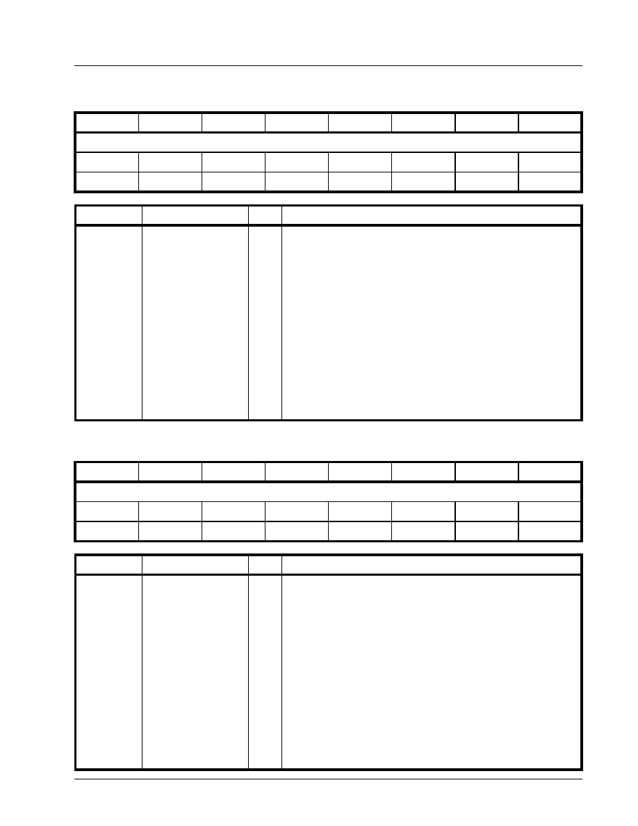
·Á
·Á
·Á
·Á
PRELIMINARY
XRT79L71
1 - CHANNEL DS3/E3 ATM UNI/PPP COMBO IC
REV. P1.0.3
365
TRANSMIT ATM CELL PROCESSOR BLOCK - TRANSMIT ATM CELL COUNTER - BYTE 2 (ADDRESS =
0X1F29)
B
IT
7
B
IT
6
B
IT
5
B
IT
4
B
IT
3
B
IT
2
B
IT
1
B
IT
0
Transmit ATM Cell Count[23:16]
RUR
RUR
RUR
RUR
RUR
RUR
RUR
RUR
0
0
0
0
0
0
0
0
B
IT
N
UMBER
N
AME
T
YPE
D
ESCRIPTION
7 - 0
Transmit ATM Cell
Count[23:16]
RUR
Transmit ATM Cell Count - Byte 2[23:16]:
This RESET-upon-READ register, along with the "Transmit ATM Cell
Count - Bytes 3, 1 and 0" registers, contain a 32-bit value for the num-
ber of User/Valid cells that have been transmitted by the Transmit ATM
Cell Processor block.
N
OTES
:
1.
The contents within these registers include all of the
following: All ATM cells that have been read out from the
TxFIFO, or the Transmit Cell Insertion Buffer.
2.
The contents of these registers do not include the number of
Idle Cells that have been generated by the Transmit ATM Cell
Processor block.
3.
If the number of Cells reaches the value "0xFFFFFFFF" then
these registers will saturate to and remain at this value (e.g.,
it will NOT overflow to "0x00000000").
TRANSMIT ATM CELL PROCESSOR BLOCK - TRANSMIT ATM CELL COUNTER - BYTE 1 (ADDRESS =
0X1F2A)
B
IT
7
B
IT
6
B
IT
5
B
IT
4
B
IT
3
B
IT
2
B
IT
1
B
IT
0
Transmit ATM Cell Count[15:8]
RUR
RUR
RUR
RUR
RUR
RUR
RUR
RUR
0
0
0
0
0
0
0
0
B
IT
N
UMBER
N
AME
T
YPE
D
ESCRIPTION
7 - 0
Transmit ATM Cell
Count[15:8]
RUR
Transmit ATM Cell Count - Byte 1[15:8]:T
his RESET-upon-READ register, along with the "Transmit ATM Cell
Count - Bytes 3, 2 and 0" registers, contain a 32-bit value for the num-
ber of User/Valid cells that have been transmitted by the Transmit ATM
Cell Processor block.
N
OTES
:
1.
The contents within these registers include all of the
following: All ATM cells that have been read out from the
TxFIFO, or the Transmit Cell Insertion Buffer.
2.
The contents of these registers do not include the number of
Idle Cells that have been generated by the Transmit ATM Cell
Processor block.
3.
If the number of Cells reaches the value "0xFFFFFFFF" then
these registers will saturate to and remain at this value (e.g.,
it will NOT overflow to "0x00000000").

XRT79L71
PRELIMINARY
·Á
·Á
·Á
·Á
REV. P1.0.3
1 - CHANNEL DS3/E3 ATM UNI/PPP COMBO IC
366
TRANSMIT ATM CELL PROCESSOR BLOCK - TRANSMIT ATM CELL COUNTER - BYTE 0 (ADDRESS =
0X1F2B)
B
IT
7
B
IT
6
B
IT
5
B
IT
4
B
IT
3
B
IT
2
B
IT
1
B
IT
0
Transmit ATM Cell Count[7:0]
RUR
RUR
RUR
RUR
RUR
RUR
RUR
RUR
0
0
0
0
0
0
0
0
B
IT
N
UMBER
N
AME
T
YPE
D
ESCRIPTION
7 - 0
Transmit ATM Cell
Count[7:0]
RUR
Transmit ATM Cell Count - Byte 0[7:0]:
This RESET-upon-READ register, along with the "Transmit ATM Cell
Count - Bytes 3 through 1" registers, contain a 32-bit value for the
number of User/Valid cells that have been transmitted by the Transmit
ATM Cell Processor block.
This particular register contains the LSB (Least Significant Byte) value
for this 32-bit expression.
N
OTES
:
1.
The contents within these registers include all of the
following: All ATM cells that have been read out from the
TxFIFO, or the Transmit Cell Insertion Buffer.
2.
The contents of these registers do not include the number of
Idle Cells that have been generated by the Transmit ATM Cell
Processor block.
3.
If the number of Cells reaches the value "0xFFFFFFFF" then
these registers will saturate to and remain at this value (e.g.,
it will NOT overflow to "0x00000000").
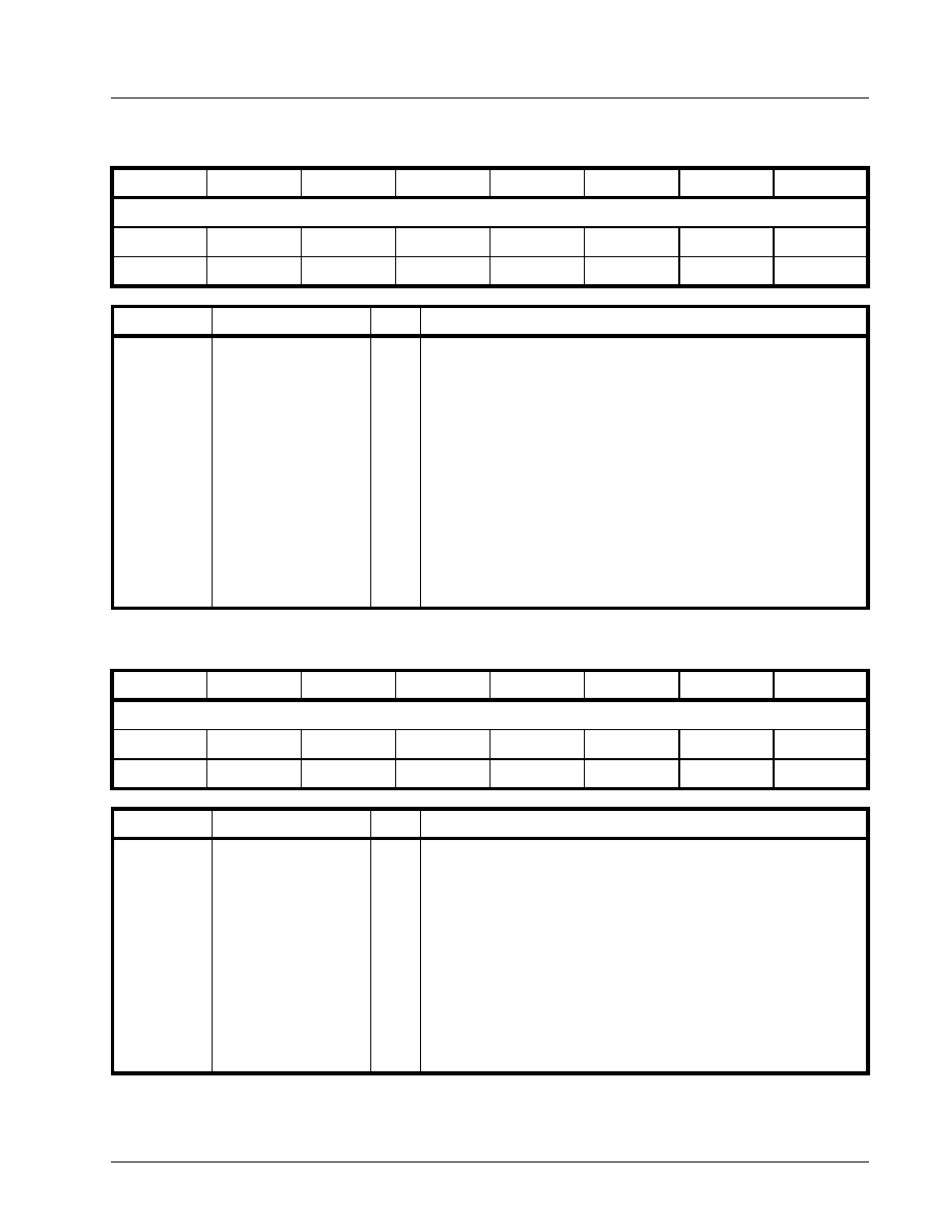
·Á
·Á
·Á
·Á
PRELIMINARY
XRT79L71
1 - CHANNEL DS3/E3 ATM UNI/PPP COMBO IC
REV. P1.0.3
367
TRANSMIT ATM CELL PROCESSOR BLOCK - TRANSMIT DISCARDED ATM CELL COUNT - BYTE 3
(ADDRESS = 0X1F2C)
B
IT
7
B
IT
6
B
IT
5
B
IT
4
B
IT
3
B
IT
2
B
IT
1
B
IT
0
Transmit - Discard Cell Count[31:24]
RUR
RUR
RUR
RUR
RUR
RUR
RUR
RUR
0
0
0
0
0
0
0
0
B
IT
N
UMBER
N
AME
T
YPE
D
ESCRIPTION
7 - 0
Transmit - Discard Cell
Count[31:24]
RUR
Transmit - Discard Cell Count - Byte 3[7:0]:
This RESET-upon-READ register, along with the "Transmit ATM Cell
Processor Block - Transmit ATM Cell Discard Cell Count - Bytes 2
through 0" registers, contain a 32-bit value for the number of ATM cells
that have been discarded by the Transmit ATM Cell Processor block.
This particular register contains the MSB (Most Significant Byte) value
of this 32-bit expression.
N
OTES
:
1.
The contents within these register includes all ATM cells that
contain either a HEC Byte error or a "Transmit UTOPIA
Parity" error.
2.
If the number of Cells reaches the value "0xFFFFFFFFF"
then these registers will saturate to and remain at this value
(e.g., it will NOT overflow to "0x00000000").
TRANSMIT ATM CELL PROCESSOR BLOCK - TRANSMIT DISCARDED ATM CELL COUNT - BYTE 2
(ADDRESS = 0X1F2D)
B
IT
7
B
IT
6
B
IT
5
B
IT
4
B
IT
3
B
IT
2
B
IT
1
B
IT
0
Transmit - Discard Cell Count[23:16]
RUR
RUR
RUR
RUR
RUR
RUR
RUR
RUR
0
0
0
0
0
0
0
0
B
IT
N
UMBER
N
AME
T
YPE
D
ESCRIPTION
7 - 0
Transmit - Discard Cell
Count[23:16]
RUR
Transmit - Discard Cell Count - Byte 2[7:0]:
This RESET-upon-READ register, along with the "Transmit ATM Cell
Processor Block - Transmit ATM Cell Discard Cell Count - Bytes 3, 1
and 0" registers, contain a 32-bit value for the number of ATM cells
that have been discarded by the Transmit ATM Cell Processor block.
N
OTES
:
1.
The contents within these register includes all ATM cells that
contain either a HEC Byte error or a "Transmit UTOPIA
Parity" error.
2.
If the number of Cells reaches the value "0xFFFFFFFFF"
then these registers will saturate to and remain at this value
(e.g., it will NOT overflow to "0x00000000").
XRT79L71
PRELIMINARY
·Á
·Á
·Á
·Á
REV. P1.0.3
1 - CHANNEL DS3/E3 ATM UNI/PPP COMBO IC
368
TRANSMIT ATM CELL PROCESSOR BLOCK - TRANSMIT DISCARDED ATM CELL COUNT - BYTE 1
(ADDRESS = 0X1F2E)
B
IT
7
B
IT
6
B
IT
5
B
IT
4
B
IT
3
B
IT
2
B
IT
1
B
IT
0
Transmit - Discard Cell Count[15:8]
RUR
RUR
RUR
RUR
RUR
RUR
RUR
RUR
0
0
0
0
0
0
0
0
B
IT
N
UMBER
N
AME
T
YPE
D
ESCRIPTION
7 - 0
Transmit - Discard Cell
Count[15:8]
RUR
Transmit - Discard Cell Count - Byte 1[7:0]:
This RESET-upon-READ register, along with the "Transmit ATM Cell
Processor Block - Transmit ATM Cell Discard Cell Count - Bytes 3, 2
and 0" registers, contain a 32-bit value for the number of ATM cells
that have been discarded by the Transmit ATM Cell Processor block.
N
OTES
:
1.
The contents within these register includes all ATM cells that
contain either a HEC Byte error or a "Transmit UTOPIA
Parity" error.
2.
If the number of Cells reaches the value "0xFFFFFFFFF"
then these registers will saturate to and remain at this value
(e.g., it will NOT overflow to "0x00000000").
TRANSMIT ATM CELL PROCESSOR BLOCK - TRANSMIT DISCARDED ATM CELL COUNT - BYTE 0
(ADDRESS = 0X1F2F)
B
IT
7
B
IT
6
B
IT
5
B
IT
4
B
IT
3
B
IT
2
B
IT
1
B
IT
0
Transmit - Discard Cell Count[7:0]
RUR
RUR
RUR
RUR
RUR
RUR
RUR
RUR
0
0
0
0
0
0
0
0
B
IT
N
UMBER
N
AME
T
YPE
D
ESCRIPTION
7 - 0
Transmit - Discard Cell
Count[7:0]
RUR
Transmit - Discard Cell Count - Byte 0[7:0]:
This RESET-upon-READ register, along with the "Transmit ATM Cell
Processor Block - Transmit ATM Cell Discard Cell Count - Bytes 3
through 1" registers, contain a 32-bit value for the number of ATM cells
that have been discarded by the Transmit ATM Cell Processor block.
This particular register contains the LSB (Least Significant Byte) value
of this 32-bit expression.
N
OTES
:
1.
The contents within these register includes all ATM cells that
contain either a HEC Byte error or a "Transmit UTOPIA
Parity" error.
2.
If the number of Cells reaches the value "0xFFFFFFFFF"
then these registers will saturate to and remain at this value
(e.g., it will NOT overflow to "0x00000000").
·Á
·Á
·Á
·Á
PRELIMINARY
XRT79L71
1 - CHANNEL DS3/E3 ATM UNI/PPP COMBO IC
REV. P1.0.3
369
TRANSMIT ATM CELL PROCESSOR BLOCK - TRANSMIT ATM HEC BYTE ERROR COUNT REGISTER -
BYTE 3 (ADDRESS = 0X1F30)
B
IT
7
B
IT
6
B
IT
5
B
IT
4
B
IT
3
B
IT
2
B
IT
1
B
IT
0
Transmit - HEC Byte Error Count[31:24]
RUR
RUR
RUR
RUR
RUR
RUR
RUR
RUR
0
0
0
0
0
0
0
0
B
IT
N
UMBER
N
AME
T
YPE
D
ESCRIPTION
7 - 0
Transmit - HEC Byte
Error Count[31:24]
RUR
Transmit - HEC Byte Error Count - Byte 3[7:0]:
his RESET-upon-READ register, along with the "Transmit ATM Cell
Processor Block - Transmit ATM HEC Byte Error Count Register -
Bytes 2 through 0" register, contain a 32-bit value for the number of
ATM cells that contain HEC byte errors (as detected by the Transmit
ATM Cell Processor block).
This particular register functions as the MSB (Most Significant Byte)
for this 32-bit expression.
N
OTES
:
1.
This register is valid if the Transmit ATM Cell Processor block
has been configured to compute and verify the HEC byte of
each ATM cell that it receives from the TxFIFO or the
"Transmit Cell Insertion Buffer".
2.
If the number of cells reaches the value "0xFFFFFFFF", then
these registers will saturate to and remain at this value (e.g.,
it will NOT overflow to "0x00000000").
TRANSMIT ATM CELL PROCESSOR BLOCK - TRANSMIT ATM HEC BYTE ERROR COUNT REGISTER -
BYTE 2 (ADDRESS = 0X1F31)
B
IT
7
B
IT
6
B
IT
5
B
IT
4
B
IT
3
B
IT
2
B
IT
1
B
IT
0
Transmit - HEC Byte Error Count[23:16]
RUR
RUR
RUR
RUR
RUR
RUR
RUR
RUR
0
0
0
0
0
0
0
0
B
IT
N
UMBER
N
AME
T
YPE
D
ESCRIPTION
7 - 0
Transmit - HEC Byte
Error Count[23:16]
RUR
Transmit - HEC Byte Error Count - Byte 2[7:0]:
This RESET-upon-READ register, along with the "Transmit ATM Cell
Processor Block - Transmit ATM HEC Byte Error Count Register -
Bytes 3, 1 and 0" register, contain a 32-bit value for the number of
ATM cells that contain HEC byte errors (as detected by the Transmit
ATM Cell Processor block).
N
OTES
:
1.
This register is valid if the Transmit ATM Cell Processor block
has been configured to compute and verify the HEC byte of
each ATM cell that it receives from the TxFIFO or the
"Transmit Cell Insertion Buffer".
2.
If the number of cells reaches the value "0xFFFFFFFF", then
these registers will saturate to and remain at this value (e.g.,
it will NOT overflow to "0x00000000").
XRT79L71
PRELIMINARY
·Á
·Á
·Á
·Á
REV. P1.0.3
1 - CHANNEL DS3/E3 ATM UNI/PPP COMBO IC
370
TRANSMIT ATM CELL PROCESSOR BLOCK - TRANSMIT ATM HEC BYTE ERROR COUNT REGISTER -
BYTE 1 (ADDRESS = 0X1F32)
B
IT
7
B
IT
6
B
IT
5
B
IT
4
B
IT
3
B
IT
2
B
IT
1
B
IT
0
Transmit - HEC Byte Error Count[15:8]
RUR
RUR
RUR
RUR
RUR
RUR
RUR
RUR
0
0
0
0
0
0
0
0
B
IT
N
UMBER
N
AME
T
YPE
D
ESCRIPTION
7 - 0
Transmit - HEC Byte
Error Count[15:8]
RUR
Transmit - HEC Byte Error Count - Byte 1[7:0]:
This RESET-upon-READ register, along with the "Transmit ATM Cell
Processor Block - Transmit ATM HEC Byte Error Count Register -
Bytes 3, 2 and 0" register, contain a 32-bit value for the number of
ATM cells that contain HEC byte errors (as detected by the Transmit
ATM Cell Processor block).
N
OTES
:
1.
This register is valid if the Transmit ATM Cell Processor block
has been configured to compute and verify the HEC byte of
each ATM cell that it receives from the TxFIFO or the
"Transmit Cell Insertion Buffer".
2.
If the number of cells reaches the value "0xFFFFFFFF", then
these registers will saturate to and remain at this value (e.g.,
it will NOT overflow to "0x00000000").
TRANSMIT ATM CELL PROCESSOR BLOCK - TRANSMIT ATM HEC BYTE ERROR COUNT REGISTER -
BYTE 0 (ADDRESS = 0X1F33)
B
IT
7
B
IT
6
B
IT
5
B
IT
4
B
IT
3
B
IT
2
B
IT
1
B
IT
0
Transmit - HEC Byte Error Count[7:0]
RUR
RUR
RUR
RUR
RUR
RUR
RUR
RUR
0
0
0
0
0
0
0
0
B
IT
N
UMBER
N
AME
T
YPE
D
ESCRIPTION
7 - 0
Transmit - HEC Byte
Error Count[7:0]
RUR
Transmit - HEC Byte Error Count - Byte 0[7:0]:
This RESET-upon-READ register, along with the "Transmit ATM Cell
Processor Block - Transmit ATM HEC Byte Error Count Register -
Bytes 3 through 1" register, contain a 32-bit value for the number of
ATM cells that contain HEC byte errors (as detected by the Transmit
ATM Cell Processor block).This particular register functions as the
LSB (Least Significant Byte) for this 32-bit expression.
N
OTES
:
1.
This register is valid if the Transmit ATM Cell Processor block
has been configured to compute and verify the HEC byte of
each ATM cell that it receives from the TxFIFO or the
"Transmit Cell Insertion Buffer".
2.
If the number of cells reaches the value "0xFFFFFFFF", then
these registers will saturate to and remain at this value (e.g.,
it will NOT overflow to "0x00000000").

·Á
·Á
·Á
·Á
PRELIMINARY
XRT79L71
1 - CHANNEL DS3/E3 ATM UNI/PPP COMBO IC
REV. P1.0.3
371
TRANSMIT ATM CELL PROCESSOR BLOCK - TRANSMIT UTOPIA PARITY ERROR COUNT REGISTER -
BYTE 3 (ADDRESS = 0X1F34)
B
IT
7
B
IT
6
B
IT
5
B
IT
4
B
IT
3
B
IT
2
B
IT
1
B
IT
0
Transmit UTOPIA - Parity Error Count[31:24]
RUR
RUR
RUR
RUR
RUR
RUR
RUR
RUR
0
0
0
0
0
0
0
0
B
IT
N
UMBER
N
AME
T
YPE
D
ESCRIPTION
7 - 0
Transmit UTOPIA -
Parity Error
Count[31:24]
RUR
Transmit UTOPIA Parity Error Count - Byte 3[7:0]:
This RESET-upon-READ register, along with the "Transmit ATM Cell
Processor Block - Transmit UTOPIA Parity Error Count Register -
Bytes 2 through 0" registers, contains a 32-bit value for the number of
ATM cells that contain "Transmit UTOPIA" Parity (byte or word) errors
(as detected by the Transmit ATM Cell Processor block).
This particular register functions as the MSB (Most Significant Byte)
for this 32-bit expression.
N
OTE
: if the number of cells reaches the value "0xFFFFFFFF", then
these registers will saturate to and remain at this value (e.g., it
will NOT overflow to "0x00000000").
TRANSMIT ATM CELL PROCESSOR BLOCK - TRANSMIT UTOPIA PARITY ERROR COUNT REGISTER -
BYTE 2 (ADDRESS = 0X1F35)
B
IT
7
B
IT
6
B
IT
5
B
IT
4
B
IT
3
B
IT
2
B
IT
1
B
IT
0
Transmit UTOPIA - Parity Error Count[23:16]
RUR
RUR
RUR
RUR
RUR
RUR
RUR
RUR
0
0
0
0
0
0
0
0
B
IT
N
UMBER
N
AME
T
YPE
D
ESCRIPTION
7 - 0
Transmit UTOPIA -
Parity Error
Count[23:16]
RUR
Transmit UTOPIA Parity Error Count - Byte 2[7:0]:
This RESET-upon-READ register, along with the "Transmit ATM Cell
Processor Block - Transmit UTOPIA Parity Error Count Register -
Bytes 3, 1 and 0" registers, contains a 32-bit value for the number of
ATM cells that contain "Transmit UTOPIA" Parity (byte or word) errors
(as detected by the Transmit ATM Cell Processor block).
N
OTE
: if the number of cells reaches the value "0xFFFFFFFF", then
these registers will saturate to and remain at this value (e.g., it
will NOT overflow to "0x00000000").

XRT79L71
PRELIMINARY
·Á
·Á
·Á
·Á
REV. P1.0.3
1 - CHANNEL DS3/E3 ATM UNI/PPP COMBO IC
372
TRANSMIT ATM CELL PROCESSOR BLOCK - TRANSMIT UTOPIA PARITY ERROR COUNT REGISTER -
BYTE 1 (ADDRESS = 0X1F36)
B
IT
7
B
IT
6
B
IT
5
B
IT
4
B
IT
3
B
IT
2
B
IT
1
B
IT
0
Transmit UTOPIA - Parity Error Count[15:8]
RUR
RUR
RUR
RUR
RUR
RUR
RUR
RUR
0
0
0
0
0
0
0
0
B
IT
N
UMBER
N
AME
T
YPE
D
ESCRIPTION
7 - 0
Transmit UTOPIA -
Parity Error
Count[15:8]
RUR
Transmit UTOPIA Parity Error Count - Byte 1[7:0]:
This RESET-upon-READ register, along with the "Transmit ATM Cell
Processor Block - Transmit UTOPIA Parity Error Count Register -
Bytes 3, 2 and 0" registers, contains a 32-bit value for the number of
ATM cells that contain "Transmit UTOPIA" Parity (byte or word) errors
(as detected by the Transmit ATM Cell Processor block).
N
OTE
: if the number of cells reaches the value "0xFFFFFFFF", then
these registers will saturate to and remain at this value (e.g., it
will NOT overflow to "0x00000000").
TRANSMIT ATM CELL PROCESSOR BLOCK - TRANSMIT UTOPIA PARITY ERROR COUNT REGISTER -
BYTE 0 (ADDRESS = 0X1F37)
B
IT
7
B
IT
6
B
IT
5
B
IT
4
B
IT
3
B
IT
2
B
IT
1
B
IT
0
Transmit UTOPIA - Parity Error Count[7:0]
RUR
RUR
RUR
RUR
RUR
RUR
RUR
RUR
0
0
0
0
0
0
0
0
B
IT
N
UMBER
N
AME
T
YPE
D
ESCRIPTION
7 - 0
Transmit UTOPIA -
Parity Error Count[7:0]
RUR
Transmit UTOPIA Parity Error Count - Byte 0[7:0]:
This RESET-upon-READ register, along with the "Transmit ATM Cell
Processor Block - Transmit UTOPIA Parity Error Count Register -
Bytes 3 through 1" registers, contains a 32-bit value for the number of
ATM cells that contain "Transmit UTOPIA" Parity (byte or word) errors
(as detected by the Transmit ATM Cell Processor block).
This particular register functions as the LSB (Least Significant Byte)
for this 32-bit expression.
N
OTE
: if the number of cells reaches the value "0xFFFFFFFF", then
these registers will saturate to and remain at this value (e.g., it
will NOT overflow to "0x00000000").

·Á
·Á
·Á
·Á
PRELIMINARY
XRT79L71
1 - CHANNEL DS3/E3 ATM UNI/PPP COMBO IC
REV. P1.0.3
373
TRANSMIT ATM CELL PROCESSOR BLOCK - TRANSMIT USER CELL FILTER CONTROL - FILTER 0
(ADDRESS = 0X1F43)
B
IT
7
B
IT
6
B
IT
5
B
IT
4
B
IT
3
B
IT
2
B
IT
1
B
IT
0
Unused
Transmit User
Cell Filter # 0
Enable
Copy Cell
Enable
Discard Cell
Enable
Filter if Pat-
tern Match
R/O
R/O
R/O
R/O
R/W
R/W
R/W
R/W
0
0
0
0
0
0
0
0
B
IT
N
UMBER
N
AME
T
YPE
D
ESCRIPTION
7 - 4
Unused
R/O
3
Transmit User Cell Fil-
ter # 0 Enable
R/W
Transmit User Cell Filter # 0 - Enable:
This READ/WRITE bit-field permits the user to either enable or dis-
able Transmit User Cell Filter # 0. If the user enables Transmit User
Cell Filter # 0, then Transmit User Cell Filter # 0 will function per the
configuration settings in Bits 2 through 0, within this register.
If the user disables Transmit User Cell Filter # 0, then Transmit User
Cell Filter # 0 then all cells that are applied to the input of Transmit
User Cell Filter # 0 will pass through to the output of Transmit User
Cell Filter # 0.
0 - Disables Transmit User Cell Filter # 0.
1 - Enables Transmit User Cell Filter # 0.
2
Copy Cell Enable
R/W
Copy Cell Enable - Transmit User Cell Filter # 0:
This READ/WRITE bit-field permits the user to either configure Trans-
mit User Cell Filter # 0 (within the Transmit ATM Cell Processor Block)
to copy all cells that have header byte patterns that comply with the
"user-defined" criteria, per Transmit User Cell Filter # 0, or to NOT
copy any of these cells.
If the user configures Transmit User Cell Filter # 0 to copy all cells
complying with a certain "header-byte" pattern, then a copy (or repli-
cate) of this "compliant" ATM cell will be routed to the Transmit Cell
Extraction Buffer.
If the user configures Transmit User Cell Filter # 0 to NOT copy all
cells complying with a certain "header-byte" pattern, then NO copies
(or replicates) of these "compliant" ATM cells will be made nor will any
be routed to the Transmit Cell Extraction Buffer.
0 - Configures Transmit User Cell Filter # 0 to NOT copy any cells that
have header byte patterns which are compliant with the "user-defined"
filtering criteria.
1 - Configures Transmit User Cell Filter # 0 to copy any cells that have
header byte patterns that are compliant with the "user-defined" filter-
ing criteria, and to route these copies (of cells) to the Transmit Cell
Extraction Buffer.
N
OTE
: This bit-field is only active if "Transmit User Cell Filter # 0" has
been enabled.

XRT79L71
PRELIMINARY
·Á
·Á
·Á
·Á
REV. P1.0.3
1 - CHANNEL DS3/E3 ATM UNI/PPP COMBO IC
374
1
Discard Cell Enable
R/W
Discard Cell Enable - Transmit User Cell Filter # 0:
This READ/WRITE bit-field permits the user to either configure Trans-
mit User Cell Filter # 0 (within the Transmit ATM Cell Processor Block)
to discard all cells that have header byte patterns that comply with the
"user-defined" criteria, per Transmit User Cell Filter # 0, or NOT dis-
card any of these cells.
If the user configures Transmit User Cell Filter # 0 to NOT discarded
any cells that is compliant with a certain "header-byte" pattern, then
the cell will be retained for further processing.
0 - Configures Transmit User Cell Filter # 0 to NOT discard any cells
that have header byte patterns that are compliant with the "user-
defined" filtering criteria.
1 - Configures Transmit User Cell Filter # 0 to discard any cells that
have header byte patterns that are compliant with the "user-defined"
filtering criteria.
N
OTE
: This bit-field is only active if "Transmit User Cell Filter # 0" has
been enabled.
0
Filter if Pattern Match
R/W
Filter if Pattern Match - Transmit User Cell Filter # 0:
This READ/WRITE bit-field permits the user to either configure Trans-
mit User Cell Filter # 0 to filter (based upon the configuration settings
for Bits 1 and 2, in this register) ATM cells with header bytes that
match the "user-defined" header byte patterns, or to filter ATM cells
with header bytes that do NOT match the "user-defined" header byte
patterns.
0 - Configures Transmit User Cell Filter # 0 to filter user cells that do
NOT match the header byte patterns (as defined in the " " registers).
1 - Configures Transmit User Cell Filter # 0 to filter user cells that do
match the header byte patterns (as defined in the " " registers).
N
OTE
: This bit-field is only active if "Transmit User Cell Filter # 0" has
been enabled.
B
IT
N
UMBER
N
AME
T
YPE
D
ESCRIPTION

·Á
·Á
·Á
·Á
PRELIMINARY
XRT79L71
1 - CHANNEL DS3/E3 ATM UNI/PPP COMBO IC
REV. P1.0.3
375
TRANSMIT ATM CELL PROCESSOR BLOCK - TRANSMIT USER CELL FILTER # 0 - PATTERN
REGISTER - HEADER BYTE 1 (ADDRESS = 0X1F44)
B
IT
7
B
IT
6
B
IT
5
B
IT
4
B
IT
3
B
IT
2
B
IT
1
B
IT
0
Transmit User Cell Filter # 0 - Pattern Register - Byte 1 [7:0]
R/W
R/W
R/W
R/W
R/W
R/W
R/W
R/W
0
0
0
0
0
0
0
0
B
IT
N
UMBER
N
AME
T
YPE
D
ESCRIPTION
7 - 0
Transmit User Cell Fil-
ter # 0 - Pattern Regis-
ter - Header Byte 1
R/W
Transmit User Cell Filter # 0 - Pattern Register - Header Byte 1:
The User Cell filtering criteria (for Transmit User Cell Filter # 0) is
defined based upon the contents of 9 read/write registers. These reg-
isters are the four "Transmit ATM Cell Processor Block - Transmit User
Cell Filter # 0 - Pattern Registers", the four "Transmit ATM Cell Proces-
sor Block - Transmit User Cell Filter # 0 - Check Registers" and the
"Transmit ATM Cell Processor Block - Transmit User Cell Filter # 0
Control Register.
This READ/WRITE register, along with the "Transmit ATM Cell Proces-
sor Block - Transmit User Cell Filter # 0 - Check Register - Header
Byte 1" permits the user to define the User Cell Filtering criteria for
"Octet # 1" of the incoming User Cell.
The user will write the header byte pattern (for Octet 1) that he/she
wishes to use as part of the "User Cell Filtering" criteria, into this reg-
ister. The user will also write in a value into the "Transmit ATM Cell
Processor Block - Transmit User Cell Filter # 0 - Check Register -
Header Byte 1" that indicates which bits within the first octet of the
incoming cells are to be compared with the contents of this register.

XRT79L71
PRELIMINARY
·Á
·Á
·Á
·Á
REV. P1.0.3
1 - CHANNEL DS3/E3 ATM UNI/PPP COMBO IC
376
TRANSMIT ATM CELL PROCESSOR BLOCK - TRANSMIT USER CELL FILTER # 0 - PATTERN
REGISTER - HEADER BYTE 2 (ADDRESS = 0X1F45)
B
IT
7
B
IT
6
B
IT
5
B
IT
4
B
IT
3
B
IT
2
B
IT
1
B
IT
0
Transmit User Cell Filter # 0 - Pattern Register - Byte 2 [7:0]
R/W
R/W
R/W
R/W
R/W
R/W
R/W
R/W
0
0
0
0
0
0
0
0
B
IT
N
UMBER
N
AME
T
YPE
D
ESCRIPTION
7 - 0
Transmit User Cell Fil-
ter # 0 - Pattern Regis-
ter - Header Byte 2
R/W
Transmit User Cell Filter # 0 - Pattern Register - Header Byte 2:
The User Cell filtering criteria (for Transmit User Cell Filter # 0) is
defined based upon the contents of 9 read/write registers. These reg-
isters are the four "Transmit ATM Cell Processor Block - Transmit User
Cell Filter # 0 - Pattern Registers", the four "Transmit ATM Cell Proces-
sor Block - Transmit User Cell Filter # 0 - Check Registers" and the
"Transmit ATM Cell Processor Block - Transmit User Cell Filter # 0
Control Register.
This READ/WRITE register, along with the "Transmit ATM Cell Proces-
sor Block - Transmit User Cell Filter # 0 - Check Register - Header
Byte 2" permits the user to define the User Cell Filtering criteria for
"Octet # 2" of the incoming User Cell.
The user will write the header byte pattern (for Octet 2) that he/she
wishes to use as part of the "User Cell Filtering" criteria, into this reg-
ister. The user will also write in a value into the "Transmit ATM Cell
Processor Block - Transmit User Cell Filter # 0 - Check Register -
Header Byte 2" that indicates which bits within the first octet of the
incoming cells are to be compared with the contents of this register.

·Á
·Á
·Á
·Á
PRELIMINARY
XRT79L71
1 - CHANNEL DS3/E3 ATM UNI/PPP COMBO IC
REV. P1.0.3
377
TRANSMIT ATM CELL PROCESSOR BLOCK - TRANSMIT USER CELL FILTER # 0 - PATTERN
REGISTER - HEADER BYTE 3 (ADDRESS = 0X1F46)
B
IT
7
B
IT
6
B
IT
5
B
IT
4
B
IT
3
B
IT
2
B
IT
1
B
IT
0
Transmit User Cell Filter # 0 - Pattern Register - Byte 3 [7:0]
R/W
R/W
R/W
R/W
R/W
R/W
R/W
R/W
0
0
0
0
0
0
0
0
B
IT
N
UMBER
N
AME
T
YPE
D
ESCRIPTION
7 - 0
Transmit User Cell Fil-
ter # 0 - Pattern Regis-
ter - Header Byte 3
R/W
Transmit User Cell Filter # 0 - Pattern Register - Header Byte 3:
The User Cell filtering criteria (for Transmit User Cell Filter # 0) is
defined based upon the contents of 9 read/write registers. These reg-
isters are the four "Transmit ATM Cell Processor Block - Transmit User
Cell Filter # 0 - Pattern Registers", the four "Transmit ATM Cell Proces-
sor Block - Transmit User Cell Filter # 0 - Check Registers" and the
"Transmit ATM Cell Processor Block - Transmit User Cell Filter # 0
Control Register.
This READ/WRITE register, along with the "Transmit ATM Cell Proces-
sor Block - Transmit User Cell Filter # 0 - Check Register - Header
Byte 3" permits the user to define the User Cell Filtering criteria for
"Octet # 3" of the incoming User Cell.
The user will write the header byte pattern (for Octet 3) that he/she
wishes to use as part of the "User Cell Filtering" criteria, into this reg-
ister. The user will also write in a value into the "Transmit ATM Cell
Processor Block - Transmit User Cell Filter # 0 - Check Register -
Header Byte 3" that indicates which bits within the first octet of the
incoming cells are to be compared with the contents of this register.

XRT79L71
PRELIMINARY
·Á
·Á
·Á
·Á
REV. P1.0.3
1 - CHANNEL DS3/E3 ATM UNI/PPP COMBO IC
378
TRANSMIT ATM CELL PROCESSOR BLOCK - TRANSMIT USER CELL FILTER # 0 - PATTERN
REGISTER - HEADER BYTE 4 (ADDRESS = 0X1F47)
B
IT
7
B
IT
6
B
IT
5
B
IT
4
B
IT
3
B
IT
2
B
IT
1
B
IT
0
Transmit User Cell Filter # 0 - Pattern Register - Byte 4 [7:0]
R/W
R/W
R/W
R/W
R/W
R/W
R/W
R/W
0
0
0
0
0
0
0
0
B
IT
N
UMBER
N
AME
T
YPE
D
ESCRIPTION
7 - 0
Transmit User Cell Fil-
ter # 0 - Pattern Regis-
ter - Header Byte 4
R/W
Transmit User Cell Filter # 0 - Pattern Register - Header Byte 4:
The User Cell filtering criteria (for Transmit User Cell Filter # 0) is
defined based upon the contents of 9 read/write registers. These reg-
isters are the four "Transmit ATM Cell Processor Block - Transmit User
Cell Filter # 0 - Pattern Registers", the four "Transmit ATM Cell Proces-
sor Block - Transmit User Cell Filter # 0 - Check Registers" and the
"Transmit ATM Cell Processor Block - Transmit User Cell Filter # 0
Control Register.
This READ/WRITE register, along with the "Transmit ATM Cell Proces-
sor Block - Transmit User Cell Filter # 0 - Check Register - Header
Byte 4" permits the user to define the User Cell Filtering criteria for
"Octet # 4" of the incoming User Cell.
The user will write the header byte pattern (for Octet 4) that he/she
wishes to use as part of the "User Cell Filtering" criteria, into this reg-
ister. The user will also write in a value into the "Transmit ATM Cell
Processor Block - Transmit User Cell Filter # 0 - Check Register -
Header Byte 4" that indicates which bits within the first octet of the
incoming cells are to be compared with the contents of this register.

·Á
·Á
·Á
·Á
PRELIMINARY
XRT79L71
1 - CHANNEL DS3/E3 ATM UNI/PPP COMBO IC
REV. P1.0.3
379
TRANSMIT ATM CELL PROCESSOR BLOCK - TRANSMIT USER CELL FILTER # 0 - CHECK REGISTER -
BYTE 1 (ADDRESS = 0X1F48)
B
IT
7
B
IT
6
B
IT
5
B
IT
4
B
IT
3
B
IT
2
B
IT
1
B
IT
0
Transmit User Cell Filter # 0 - Check Register - Byte 1 [7:0]
R/W
R/W
R/W
R/W
R/W
R/W
R/W
R/W
0
0
0
0
0
0
0
0
B
IT
N
UMBER
N
AME
T
YPE
D
ESCRIPTION
7 - 0
Transmit User Cell Fil-
ter # 0 - Check Regis-
ter - Header Byte 1
R/W
Transmit User Cell Filter # 0 - Check Register - Header Byte 1:
The User Cell filtering criteria (for Transmit User Cell Filter # 0) is
defined based upon the contents of 9 read/write registers. These reg-
isters are the four "Transmit ATM Cell Processor Block - Transmit User
Cell Filter # 0 - Pattern Registers", the four "Transmit ATM Cell Proces-
sor Block - Transmit User Cell Filter # 0 - Check Registers" and the
"Transmit ATM Cell Processor Block - Transmit User Cell Filter # 0
Control Register.
This READ/WRITE register, along with the "Transmit ATM Cell Proces-
sor Block - Transmit User Cell Filter # 0 - Pattern Register - Header
Byte 1" permits the user to define the User Cell Filtering criteria for
"Octet # 1" within the incoming User Cell. More specifically, these
READ/WRITE register bits permit the user to specify which bit(s) in
"Octet 1" of the incoming user cell (in the Transmit ATM Cell Processor
Block) are to be checked against the corresponding bit-fields within
the "Transmit ATM Cell Processor Block - Transmit User Cell Filter # 0
- Pattern Register - Header Byte 1" by the User Cell Filter, when deter-
mine whether to "filter" a given User Cell.
Writing a "1" to a particular bit-field in this register, forces the Transmit
User Cell Filter to check and compare the corresponding bit in "Octet
# 1" (of the incoming user cell) with the corresponding bit in the
"Transmit ATM Cell Processor Block - Transmit User Cell Filter # 0 -
Pattern Register - Header Byte 1".
Writing a "0" to a particular bit-field in this register causes the Transmit
User Cell Filter to treat the corresponding bit within "Octet # 1" (in the
incoming user cell) as a "don't care" (e.g., to forgo the comparison
between the corresponding bit in "Octet # 1" of the incoming user cell
with the corresponding bit-field in the "Transmit ATM Cell Processor
Block - Transmit User Cell Filter # 0 - Pattern Register - Header Byte
1").

XRT79L71
PRELIMINARY
·Á
·Á
·Á
·Á
REV. P1.0.3
1 - CHANNEL DS3/E3 ATM UNI/PPP COMBO IC
380
TRANSMIT ATM CELL PROCESSOR BLOCK - TRANSMIT USER CELL FILTER # 0 - CHECK REGISTER -
BYTE 2 (ADDRESS = 0X1F49)
B
IT
7
B
IT
6
B
IT
5
B
IT
4
B
IT
3
B
IT
2
B
IT
1
B
IT
0
Transmit User Cell Filter # 0 - Check Register - Byte 2 [7:0]
R/W
R/W
R/W
R/W
R/W
R/W
R/W
R/W
0
0
0
0
0
0
0
0
B
IT
N
UMBER
N
AME
T
YPE
D
ESCRIPTION
7 - 0
Transmit User Cell Fil-
ter # 0 - Check Regis-
ter - Header Byte 2
R/W
Transmit User Cell Filter # 0 - Check Register - Header Byte 2:
The User Cell filtering criteria (for Transmit User Cell Filter # 0) is
defined based upon the contents of 9 read/write registers. These reg-
isters are the four "Transmit ATM Cell Processor Block - Transmit User
Cell Filter # 0 - Pattern Registers", the four "Transmit ATM Cell Proces-
sor Block - Transmit User Cell Filter # 0 - Check Registers" and the
"Transmit ATM Cell Processor Block - Transmit User Cell Filter # 0
Control Register.
This READ/WRITE register, along with the "Transmit ATM Cell Proces-
sor Block - Transmit User Cell Filter # 0 - Pattern Register - Header
Byte 2" permits the user to define the User Cell Filtering criteria for
"Octet # 2" within the incoming User Cell. More specifically, these
READ/WRITE register bits permit the user to specify which bit(s) in
"Octet 2" of the incoming user cell (in the Transmit ATM Cell Processor
Block) are to be checked against the corresponding bit-fields within
the "Transmit ATM Cell Processor Block - Transmit User Cell Filter # 0
- Pattern Register - Header Byte 2" by the User Cell Filter, when deter-
mine whether to "filter" a given User Cell.
Writing a "1" to a particular bit-field in this register, forces the Transmit
User Cell Filter to check and compare the corresponding bit in "Octet
# 2" (of the incoming user cell) with the corresponding bit in the
"Transmit ATM Cell Processor Block - Transmit User Cell Filter # 0 -
Pattern Register - Header Byte 2".
Writing a "0" to a particular bit-field in this register causes the Transmit
User Cell Filter to treat the corresponding bit within "Octet # 2" (in the
incoming user cell) as a "don't care" (e.g., to forgo the comparison
between the corresponding bit in "Octet # 2" of the incoming user cell
with the corresponding bit-field in the "Transmit ATM Cell Processor
Block - Transmit User Cell Filter # 0 - Pattern Register - Header Byte
2").

·Á
·Á
·Á
·Á
PRELIMINARY
XRT79L71
1 - CHANNEL DS3/E3 ATM UNI/PPP COMBO IC
REV. P1.0.3
381
TRANSMIT ATM CELL PROCESSOR BLOCK - TRANSMIT USER CELL FILTER # 0 - CHECK REGISTER -
BYTE 3 (ADDRESS = 0X1F4A)
B
IT
7
B
IT
6
B
IT
5
B
IT
4
B
IT
3
B
IT
2
B
IT
1
B
IT
0
Transmit User Cell Filter # 0 - Check Register - Byte 3 [7:0]
R/W
R/W
R/W
R/W
R/W
R/W
R/W
R/W
0
0
0
0
0
0
0
0
B
IT
N
UMBER
N
AME
T
YPE
D
ESCRIPTION
7 - 0
Transmit User Cell Fil-
ter # 0 - Check Regis-
ter - Header Byte 3
R/W
Transmit User Cell Filter # 0 - Check Register - Header Byte 3:
The User Cell filtering criteria (for Transmit User Cell Filter # 0) is
defined based upon the contents of 9 read/write registers. These reg-
isters are the four "Transmit ATM Cell Processor Block - Transmit User
Cell Filter # 0 - Pattern Registers", the four "Transmit ATM Cell Proces-
sor Block - Transmit User Cell Filter # 0 - Check Registers" and the
"Transmit ATM Cell Processor Block - Transmit User Cell Filter # 0
Control Register.
This READ/WRITE register, along with the "Transmit ATM Cell Proces-
sor Block - Transmit User Cell Filter # 0 - Pattern Register - Header
Byte 3" permits the user to define the User Cell Filtering criteria for
"Octet # 3" within the incoming User Cell. More specifically, these
READ/WRITE register bits permit the user to specify which bit(s) in
"Octet 3" of the incoming user cell (in the Transmit ATM Cell Processor
Block) are to be checked against the corresponding bit-fields within
the "Transmit ATM Cell Processor Block - Transmit User Cell Filter # 0
- Pattern Register - Header Byte 3" by the User Cell Filter, when deter-
mine whether to "filter" a given User Cell.
Writing a "1" to a particular bit-field in this register, forces the Transmit
User Cell Filter to check and compare the corresponding bit in "Octet
# 3" (of the incoming user cell) with the corresponding bit in the
"Transmit ATM Cell Processor Block - Transmit User Cell Filter # 0 -
Pattern Register - Header Byte 3".
Writing a "0" to a particular bit-field in this register causes the Transmit
User Cell Filter to treat the corresponding bit within "Octet # 3" (in the
incoming user cell) as a "don't care" (e.g., to forgo the comparison
between the corresponding bit in "Octet # 3" of the incoming user cell
with the corresponding bit-field in the "Transmit ATM Cell Processor
Block - Transmit User Cell Filter # 0 - Pattern Register - Header Byte
3").

XRT79L71
PRELIMINARY
·Á
·Á
·Á
·Á
REV. P1.0.3
1 - CHANNEL DS3/E3 ATM UNI/PPP COMBO IC
382
TRANSMIT ATM CELL PROCESSOR BLOCK - TRANSMIT USER CELL FILTER # 0 - CHECK REGISTER -
BYTE 4 (ADDRESS = 0X1F4B)
B
IT
7
B
IT
6
B
IT
5
B
IT
4
B
IT
3
B
IT
2
B
IT
1
B
IT
0
Transmit User Cell Filter # 0 - Check Register - Byte 4 [7:0]
R/W
R/W
R/W
R/W
R/W
R/W
R/W
R/W
0
0
0
0
0
0
0
0
B
IT
N
UMBER
N
AME
T
YPE
D
ESCRIPTION
7 - 0
Transmit User Cell Fil-
ter # 0 - Check Regis-
ter - Header Byte 4
R/W
Transmit User Cell Filter # 0 - Check Register - Header Byte 4:
The User Cell filtering criteria (for Transmit User Cell Filter # 0) is
defined based upon the contents of 9 read/write registers. These reg-
isters are the four "Transmit ATM Cell Processor Block - Transmit User
Cell Filter # 0 - Pattern Registers", the four "Transmit ATM Cell Proces-
sor Block - Transmit User Cell Filter # 0 - Check Registers" and the
"Transmit ATM Cell Processor Block - Transmit User Cell Filter # 0
Control Register.
This READ/WRITE register, along with the "Transmit ATM Cell Proces-
sor Block - Transmit User Cell Filter # 0 - Pattern Register - Header
Byte 4" permits the user to define the User Cell Filtering criteria for
"Octet # 4" within the incoming User Cell. More specifically, these
READ/WRITE register bits permit the user to specify which bit(s) in
"Octet 4" of the incoming user cell (in the Transmit ATM Cell Processor
Block) are to be checked against the corresponding bit-fields within
the "Transmit ATM Cell Processor Block - Transmit User Cell Filter # 0
- Pattern Register - Header Byte 4" by the User Cell Filter, when deter-
mine whether to "filter" a given User Cell.
Writing a "1" to a particular bit-field in this register, forces the Transmit
User Cell Filter to check and compare the corresponding bit in "Octet
# 4" (of the incoming user cell) with the corresponding bit in the
"Transmit ATM Cell Processor Block - Transmit User Cell Filter # 0 -
Pattern Register - Header Byte 4".
Writing a "0" to a particular bit-field in this register causes the Transmit
User Cell Filter to treat the corresponding bit within "Octet # 4" (in the
incoming user cell) as a "don't care" (e.g., to forgo the comparison
between the corresponding bit in "Octet # 4" of the incoming user cell
with the corresponding bit-field in the "Transmit ATM Cell Processor
Block - Transmit User Cell Filter # 0 - Pattern Register - Header Byte
4").

·Á
·Á
·Á
·Á
PRELIMINARY
XRT79L71
1 - CHANNEL DS3/E3 ATM UNI/PPP COMBO IC
REV. P1.0.3
383
TRANSMIT ATM CELL PROCESSOR BLOCK - TRANSMIT USER CELL FILTER # 0 - FILTERED CELL
COUNT - BYTE 3 (ADDRESS = 0X1F4C)
B
IT
7
B
IT
6
B
IT
5
B
IT
4
B
IT
3
B
IT
2
B
IT
1
B
IT
0
Transmit User Cell Filter # 0 - Filtered Cell Count[31:24]
RUR
RUR
RUR
RUR
RUR
RUR
RUR
RUR
0
0
0
0
0
0
0
0
B
IT
N
UMBER
N
AME
T
YPE
D
ESCRIPTION
7 - 0
Transmit User Cell Fil-
ter # 0 - Filtered Cell
Count[31:24]
RUR
Transmit User Cell Filter # 0 - Filtered Cell Count[31:24]:
These RESET-upon-READ bit-fields, along with that in the "Transmit
ATM Cell Processor Block - Transmit User Cell Filter # 0 - Filtered Cell
Count - Bytes 2" through "0" register contain a 32-bit expression for
the number of User Cells that have been filtered by Transmit User Cell
Filter # 0 since the last read of this register.
Depending upon the configuration settings within the "Transmit ATM
Cell Processor Block - Transmit User Cell Filter Control - User Cell Fil-
ter # 0" Register (Address = 0x1F43), these register bits will be incre-
mented anytime User Cell Filter # 0 performs any of the following
functions.
∑
Discards an incoming "User Cell".
∑
Copies (or Replicates) an incoming "User Cell" and routes the
"copy" to the Transmit Cell Extraction Buffer.
∑
both the above actions.
This particular register contains the MSB (Most Significant Byte) value
for this 32-bit expression.
N
OTE
: If the number of "filtered cells" reaches the value
"0xFFFFFFFF" then these registers will saturate to and
remain at this value (e.g., it will not overflow to "0x00000000").

XRT79L71
PRELIMINARY
·Á
·Á
·Á
·Á
REV. P1.0.3
1 - CHANNEL DS3/E3 ATM UNI/PPP COMBO IC
384
TRANSMIT ATM CELL PROCESSOR BLOCK - TRANSMIT USER CELL FILTER # 0 - FILTERED CELL
COUNT - BYTE 2 (ADDRESS = 0X1F4D)
B
IT
7
B
IT
6
B
IT
5
B
IT
4
B
IT
3
B
IT
2
B
IT
1
B
IT
0
Transmit User Cell Filter # 0 - Filtered Cell Count[23:16]
RUR
RUR
RUR
RUR
RUR
RUR
RUR
RUR
0
0
0
0
0
0
0
0
B
IT
N
UMBER
N
AME
T
YPE
D
ESCRIPTION
7 - 0
Transmit User Cell Fil-
ter # 0 - Filtered Cell
Count[23:16]
RUR
Transmit User Cell Filter # 0 - Filtered Cell Count[23:16]:
These RESET-upon-READ bit-fields, along with that in the "Transmit
ATM Cell Processor Block - Transmit User Cell Filter # 0 - Filtered Cell
Count - Bytes 3, 1 and 0" register contain a 32-bit expression for the
number of User Cells that have been filtered by Transmit User Cell Fil-
ter # 0 since the last read of this register.
Depending upon the configuration settings within the "Transmit ATM
Cell Processor Block - Transmit User Cell Filter Control - Transmit
User Cell Filter # 0" Register (Address = 0x1F43), these register bits
will be incremented anytime User Cell Filter # 0 performs any of the
following functions.
∑
Discards an incoming "User Cell".
∑
Copies (or Replicates) an incoming "User Cell" and routes the
"copy" to the Transmit Cell Extraction Buffer.
∑
both the above actions.
N
OTE
: If the number of "filtered cells" reaches the value
"0xFFFFFFFF" then these registers will saturate to and
remain at this value (e.g., it will not overflow to "0x00000000").

·Á
·Á
·Á
·Á
PRELIMINARY
XRT79L71
1 - CHANNEL DS3/E3 ATM UNI/PPP COMBO IC
REV. P1.0.3
385
TRANSMIT ATM CELL PROCESSOR BLOCK - TRANSMIT USER CELL FILTER # 0 - FILTERED CELL
COUNT - BYTE 1 (ADDRESS = 0X1F4E)
B
IT
7
B
IT
6
B
IT
5
B
IT
4
B
IT
3
B
IT
2
B
IT
1
B
IT
0
Transmit User Cell Filter # 0 - Filtered Cell Count[15:8]
RUR
RUR
RUR
RUR
RUR
RUR
RUR
RUR
0
0
0
0
0
0
0
0
B
IT
N
UMBER
N
AME
T
YPE
D
ESCRIPTION
7 - 0
Transmit User Cell Fil-
ter # 0 - Filtered Cell
Count[15:8]
RUR
Transmit User Cell Filter # 0 - Filtered Cell Count[15:8]:
These RESET-upon-READ bit-fields, along with that in the "Transmit
ATM Cell Processor Block - Transmit User Cell Filter # 0 - Filtered Cell
Count - Bytes 3, 2 and 0" register contain a 32-bit expression for the
number of User Cells that have been filtered by Transmit User Cell Fil-
ter # 0 since the last read of this register.
Depending upon the configuration settings within the "Transmit ATM
Cell Processor Block - Transmit User Cell Filter Control - Transmit
User Cell Filter # 0" Register (Address = 0x1F43), these register bits
will be incremented anytime Transmit User Cell Filter # 0 performs any
of the following functions.
∑
Discards an incoming "User Cell".
∑
Copies (or Replicates) an incoming "User Cell" and routes the
"copy" to the Transmit Cell Extraction Buffer.
∑
both the above actions.
N
OTE
: If the number of "filtered cells" reaches the value
"0xFFFFFFFF" then these registers will saturate to and
remain at this value (e.g., it will not overflow to "0x00000000").

XRT79L71
PRELIMINARY
·Á
·Á
·Á
·Á
REV. P1.0.3
1 - CHANNEL DS3/E3 ATM UNI/PPP COMBO IC
386
TRANSMIT ATM CELL PROCESSOR BLOCK - TRANSMIT USER CELL FILTER # 0 - FILTERED CELL
COUNT - BYTE 0 (ADDRESS = 0X1F4F)
B
IT
7
B
IT
6
B
IT
5
B
IT
4
B
IT
3
B
IT
2
B
IT
1
B
IT
0
Transmit User Cell Filter # 0 - Filtered Cell Count[7:0]
RUR
RUR
RUR
RUR
RUR
RUR
RUR
RUR
0
0
0
0
0
0
0
0
B
IT
N
UMBER
N
AME
T
YPE
D
ESCRIPTION
7 - 0
Transmit User Cell Fil-
ter # 0 - Filtered Cell
Count[7:0]
RUR
Transmit User Cell Filter # 0 - Filtered Cell Count[7:0]:
These RESET-upon-READ bit-fields, along with that in the "Transmit
ATM Cell Processor Block - Transmit User Cell Filter # 0 - Filtered Cell
Count - Bytes 3" through "1" register contain a 32-bit expression for
the number of User Cells that have been filtered by Transmit User Cell
Filter # 0 since the last read of this register.
Depending upon the configuration settings within the "Transmit ATM
Cell Processor Block - Transmit User Cell Filter Control - Transmit
User Cell Filter # 0" Register (Address = 0x1F43), these register bits
will be incremented anytime Transmit User Cell Filter # 0 performs any
of the following functions.
∑
Discards an incoming "User Cell".
∑
Copies (or Replicates) an incoming "User Cell" and routes the
"copy" to the Transmit Cell Extraction Buffer.
∑
both the above actions.
This particular register contains the LSB (Least Significant Byte) value
for this 32-bit expression.
N
OTE
: If the number of "filtered cells" reaches the value
"0xFFFFFFFF" then these registers will saturate to and
remain at this value (e.g., it will not overflow to "0x00000000").

·Á
·Á
·Á
·Á
PRELIMINARY
XRT79L71
1 - CHANNEL DS3/E3 ATM UNI/PPP COMBO IC
REV. P1.0.3
387
TRANSMIT ATM CELL PROCESSOR BLOCK - TRANSMIT USER CELL FILTER CONTROL - FILTER 1
(ADDRESS = 0X1F53)
B
IT
7
B
IT
6
B
IT
5
B
IT
4
B
IT
3
B
IT
2
B
IT
1
B
IT
0
Unused
Transmit User
Cell Filter # 1
Enable
Copy Cell
Enable
Discard Cell
Enable
Filter if
Pattern Match
R/O
R/O
R/O
R/O
R/W
R/W
R/W
R/W
0
0
0
0
0
0
0
0
B
IT
N
UMBER
N
AME
T
YPE
D
ESCRIPTION
7 - 4
Unused
R/O
3
Transmit User Cell Fil-
ter # 1 Enable
R/W
Transmit User Cell Filter # 1 - Enable:
This READ/WRITE bit-field permits the user to either enable or dis-
able Transmit User Cell Filter # 1. If the user enables Transmit User
Cell Filter # 1, then Transmit User Cell Filter # 1 will function per the
configuration settings in Bits 2 through 0, within this register.
If the user disables Transmit User Cell Filter # 1, then Transmit User
Cell Filter # 1 then all cells that are applied to the input of Transmit
User Cell Filter # 1 will pass through to the output of Transmit User
Cell Filter # 1.
0 - Disables Transmit User Cell Filter # 1.
1 - Enables Transmit User Cell Filter # 1.
2
Copy Cell Enable
R/W
Copy Cell Enable - Transmit User Cell Filter # 1:
This READ/WRITE bit-field permits the user to either configure Trans-
mit User Cell Filter # 1 (within the Transmit ATM Cell Processor Block)
to copy all cells that have header byte patterns that comply with the
"user-defined" criteria, per Transmit User Cell Filter # 1, or to NOT
copy any of these cells.
If the user configures Transmit User Cell Filter # 1 to copy all cells
complying with a certain "header-byte" pattern, then a copy (or repli-
cate) of this "compliant" ATM cell will be routed to the Transmit Cell
Extraction Buffer.
If the user configures Transmit User Cell Filter # 1 to NOT copy all
cells complying with a certain "header-byte" pattern, then NO copies
(or replicates) of these "compliant" ATM cells will be made nor will any
be routed to the Transmit Cell Extraction Buffer.
0 - Configures Transmit User Cell Filter # 1 to NOT copy any cells that
have header byte patterns which are compliant with the "user-defined"
filtering criteria.
1 - Configures Transmit User Cell Filter # 1 to copy any cells that have
header byte patterns that are compliant with the "user-defined" filter-
ing criteria, and to route these copies (of cells) to the Transmit Cell
Extraction Buffer.
N
OTE
: This bit-field is only active if "Transmit User Cell Filter # 1" has
been enabled.

XRT79L71
PRELIMINARY
·Á
·Á
·Á
·Á
REV. P1.0.3
1 - CHANNEL DS3/E3 ATM UNI/PPP COMBO IC
388
1
Discard Cell Enable
R/W
Discard Cell Enable - Transmit User Cell Filter # 1:
This READ/WRITE bit-field permits the user to either configure Trans-
mit User Cell Filter # 1 (within the Transmit ATM Cell Processor Block)
to discard all cells that have header byte patterns that comply with the
"user-defined" criteria, per Transmit User Cell Filter # 1, or NOT dis-
card any of these cells.
If the user configures Transmit User Cell Filter # 1 to NOT discarded
any cells that is compliant with a certain "header-byte" pattern, then
the cell will be retained for further processing.
0 - Configures Transmit User Cell Filter # 1 to NOT discard any cells
that have header byte patterns that are compliant with the "user-
defined" filtering criteria.
1 - Configures Transmit User Cell Filter # 1 to discard any cells that
have header byte patterns that are compliant with the "user-defined"
filtering criteria.
N
OTE
: This bit-field is only active if "Transmit User Cell Filter # 1" has
been enabled.
0
Filter if Pattern Match
R/W
Filter if Pattern Match - Transmit User Cell Filter # 1:
This READ/WRITE bit-field permits the user to either configure Trans-
mit User Cell Filter # 1 to filter (based upon the configuration settings
for Bits 1 and 2, in this register) ATM cells with header bytes that
match the "user-defined" header byte patterns, or to filter ATM cells
with header bytes that do NOT match the "user-defined" header byte
patterns.
0 - Configures Transmit User Cell Filter # 1 to filter user cells that do
NOT match the header byte patterns (as defined in the " " registers).
1 - Configures Transmit User Cell Filter # 1 to filter user cells that do
match the header byte patterns (as defined in the " " registers).
N
OTE
: This bit-field is only active if "Transmit User Cell Filter # 1" has
been enabled.
B
IT
N
UMBER
N
AME
T
YPE
D
ESCRIPTION

·Á
·Á
·Á
·Á
PRELIMINARY
XRT79L71
1 - CHANNEL DS3/E3 ATM UNI/PPP COMBO IC
REV. P1.0.3
389
TRANSMIT ATM CELL PROCESSOR BLOCK - TRANSMIT USER CELL FILTER # 1 - PATTERN
REGISTER - HEADER BYTE 1 (ADDRESS = 0X1F54)
B
IT
7
B
IT
6
B
IT
5
B
IT
4
B
IT
3
B
IT
2
B
IT
1
B
IT
0
Transmit User Cell Filter # 1 - Pattern Register - Byte 1 [7:0]
R/W
R/W
R/W
R/W
R/W
R/W
R/W
R/W
0
0
0
0
0
0
0
0
B
IT
N
UMBER
N
AME
T
YPE
D
ESCRIPTION
7 - 0
Transmit User Cell Fil-
ter # 1 - Pattern Regis-
ter - Header Byte 1
R/W
Transmit User Cell Filter # 1 - Pattern Register - Header Byte 1:
The User Cell filtering criteria (for Transmit User Cell Filter # 1) is
defined based upon the contents of 9 read/write registers.
These registers are the four "Transmit ATM Cell Processor Block -
Transmit User Cell Filter # 1 - Pattern Registers", the four "Transmit
ATM Cell Processor Block - Transmit User Cell Filter # 1 - Check Reg-
isters" and the "Transmit ATM Cell Processor Block - Transmit User
Cell Filter # 1 Control Register.
This READ/WRITE register, along with the "Transmit ATM Cell Proces-
sor Block - Transmit User Cell Filter # 1 - Check Register - Header
Byte 1" permits the user to define the User Cell Filtering criteria for
"Octet # 1" of the incoming User Cell.
The user will write the header byte pattern (for Octet 1) that he/she
wishes to use as part of the "User Cell Filtering" criteria, into this reg-
ister.
The user will also write in a value into the "Transmit ATM Cell Proces-
sor Block - Transmit User Cell Filter # 1 - Check Register - Header
Byte 1" that indicates which bits within the first octet of the incoming
cells are to be compared with the contents of this register.

XRT79L71
PRELIMINARY
·Á
·Á
·Á
·Á
REV. P1.0.3
1 - CHANNEL DS3/E3 ATM UNI/PPP COMBO IC
390
TRANSMIT ATM CELL PROCESSOR BLOCK - TRANSMIT USER CELL FILTER # 1 - PATTERN
REGISTER - HEADER BYTE 2 (ADDRESS = 0X1F55)
B
IT
7
B
IT
6
B
IT
5
B
IT
4
B
IT
3
B
IT
2
B
IT
1
B
IT
0
Transmit User Cell Filter # 1 - Pattern Register - Byte 2 [7:0]
R/W
R/W
R/W
R/W
R/W
R/W
R/W
R/W
0
0
0
0
0
0
0
0
B
IT
N
UMBER
N
AME
T
YPE
D
ESCRIPTION
7 - 0
Transmit User Cell Fil-
ter # 1 - Pattern Regis-
ter - Header Byte 2
R/W
Transmit User Cell Filter # 1 - Pattern Register - Header Byte 2:
The User Cell filtering criteria (for Transmit User Cell Filter # 1) is
defined based upon the contents of 9 read/write registers.
These registers are the four "Transmit ATM Cell Processor Block -
Transmit User Cell Filter # 1 - Pattern Registers", the four "Transmit
ATM Cell Processor Block - Transmit User Cell Filter # 1 - Check Reg-
isters" and the "Transmit ATM Cell Processor Block - Transmit User
Cell Filter # 1 Control Register.
This READ/WRITE register, along with the "Transmit ATM Cell Proces-
sor Block - Transmit User Cell Filter # 1 - Check Register - Header
Byte 2" permits the user to define the User Cell Filtering criteria for
"Octet # 2" of the incoming User Cell.
The user will write the header byte pattern (for Octet 2) that he/she
wishes to use as part of the "User Cell Filtering" criteria, into this reg-
ister.
The user will also write in a value into the "Transmit ATM Cell Proces-
sor Block - Transmit User Cell Filter # 1 - Check Register - Header
Byte 2" that indicates which bits within the first octet of the incoming
cells are to be compared with the contents of this register.

·Á
·Á
·Á
·Á
PRELIMINARY
XRT79L71
1 - CHANNEL DS3/E3 ATM UNI/PPP COMBO IC
REV. P1.0.3
391
TRANSMIT ATM CELL PROCESSOR BLOCK - TRANSMIT USER CELL FILTER # 1 - PATTERN
REGISTER - HEADER BYTE 3 (ADDRESS = 0X1F56)
B
IT
7
B
IT
6
B
IT
5
B
IT
4
B
IT
3
B
IT
2
B
IT
1
B
IT
0
Transmit User Cell Filter # 1 - Pattern Register - Byte 3 [7:0]
R/W
R/W
R/W
R/W
R/W
R/W
R/W
R/W
0
0
0
0
0
0
0
0
B
IT
N
UMBER
N
AME
T
YPE
D
ESCRIPTION
7 - 0
Transmit User Cell Fil-
ter # 1 - Pattern Regis-
ter - Header Byte 3
R/W
Transmit User Cell Filter # 1 - Pattern Register - Header Byte 3:
The User Cell filtering criteria (for Transmit User Cell Filter # 1) is
defined based upon the contents of 9 read/write registers.
These registers are the four "Transmit ATM Cell Processor Block -
Transmit User Cell Filter # 1 - Pattern Registers", the four "Transmit
ATM Cell Processor Block - Transmit User Cell Filter # 1 - Check Reg-
isters" and the "Transmit ATM Cell Processor Block - Transmit User
Cell Filter # 1 Control Register.
This READ/WRITE register, along with the "Transmit ATM Cell Proces-
sor Block - Transmit User Cell Filter # 1 - Check Register - Header
Byte 3" permits the user to define the User Cell Filtering criteria for
"Octet # 3" of the incoming User Cell.
The user will write the header byte pattern (for Octet 3) that he/she
wishes to use as part of the "User Cell Filtering" criteria, into this reg-
ister.
The user will also write in a value into the "Transmit ATM Cell Proces-
sor Block - Transmit User Cell Filter # 1 - Check Register - Header
Byte 3" that indicates which bits within the first octet of the incoming
cells are to be compared with the contents of this register.

XRT79L71
PRELIMINARY
·Á
·Á
·Á
·Á
REV. P1.0.3
1 - CHANNEL DS3/E3 ATM UNI/PPP COMBO IC
392
TRANSMIT ATM CELL PROCESSOR BLOCK - TRANSMIT USER CELL FILTER # 1 - PATTERN
REGISTER - HEADER BYTE 4 (ADDRESS = 0X1F57)
B
IT
7
B
IT
6
B
IT
5
B
IT
4
B
IT
3
B
IT
2
B
IT
1
B
IT
0
Transmit User Cell Filter # 1 - Pattern Register - Byte 4 [7:0]
R/W
R/W
R/W
R/W
R/W
R/W
R/W
R/W
0
0
0
0
0
0
0
0
B
IT
N
UMBER
N
AME
T
YPE
D
ESCRIPTION
7 - 0
Transmit User Cell Fil-
ter # 1 - Pattern Regis-
ter - Header Byte 4
R/W
Transmit User Cell Filter # 1 - Pattern Register - Header Byte 4:
The User Cell filtering criteria (for Transmit User Cell Filter # 1) is
defined based upon the contents of 9 read/write registers.
These registers are the four "Transmit ATM Cell Processor Block -
Transmit User Cell Filter # 1 - Pattern Registers", the four "Transmit
ATM Cell Processor Block - Transmit User Cell Filter # 1 - Check Reg-
isters" and the "Transmit ATM Cell Processor Block - Transmit User
Cell Filter # 1 Control Register.
This READ/WRITE register, along with the "Transmit ATM Cell Proces-
sor Block - Transmit User Cell Filter # 1 - Check Register - Header
Byte 4" permits the user to define the User Cell Filtering criteria for
"Octet # 4" of the incoming User Cell.
The user will write the header byte pattern (for Octet 4) that he/she
wishes to use as part of the "User Cell Filtering" criteria, into this reg-
ister.
The user will also write in a value into the "Transmit ATM Cell Proces-
sor Block - Transmit User Cell Filter # 1 - Check Register - Header
Byte 4" that indicates which bits within the first octet of the incoming
cells are to be compared with the contents of this register.

·Á
·Á
·Á
·Á
PRELIMINARY
XRT79L71
1 - CHANNEL DS3/E3 ATM UNI/PPP COMBO IC
REV. P1.0.3
393
TRANSMIT ATM CELL PROCESSOR BLOCK - TRANSMIT USER CELL FILTER # 1 - CHECK REGISTER -
BYTE 1 (ADDRESS = 0X1F58)
B
IT
7
B
IT
6
B
IT
5
B
IT
4
B
IT
3
B
IT
2
B
IT
1
B
IT
0
Transmit User Cell Filter # 1 - Check Register - Byte 1 [7:0]
R/W
R/W
R/W
R/W
R/W
R/W
R/W
R/W
0
0
0
0
0
0
0
0
B
IT
N
UMBER
N
AME
T
YPE
D
ESCRIPTION
7 - 0
Transmit User Cell Fil-
ter # 1 - Check Regis-
ter - Header Byte 1
R/W
Transmit User Cell Filter # 1 - Check Register - Header Byte 1:
The User Cell filtering criteria (for Transmit User Cell Filter # 1) is
defined based upon the contents of 9 read/write registers.
These registers are the four "Transmit ATM Cell Processor Block -
Transmit User Cell Filter # 1 - Pattern Registers", the four "Transmit
ATM Cell Processor Block - Transmit User Cell Filter # 1 - Check Reg-
isters" and the "Transmit ATM Cell Processor Block - Transmit User
Cell Filter # 1 Control Register.
This READ/WRITE register, along with the "Transmit ATM Cell Proces-
sor Block - Transmit User Cell Filter # 1 - Pattern Register - Header
Byte 1" permits the user to define the User Cell Filtering criteria for
"Octet # 1" within the incoming User Cell. More specifically, these
READ/WRITE register bits permit the user to specify which bit(s) in
"Octet 1" of the incoming user cell (in the Transmit ATM Cell Processor
Block) are to be checked against the corresponding bit-fields within
the "Transmit ATM Cell Processor Block - Transmit User Cell Filter # 1
- Pattern Register - Header Byte 1" by the User Cell Filter, when deter-
mine whether to "filter" a given User Cell.
Writing a "1" to a particular bit-field in this register, forces the Transmit
User Cell Filter to check and compare the corresponding bit in "Octet
# 1" (of the incoming user cell) with the corresponding bit in the
"Transmit ATM Cell Processor Block - Transmit User Cell Filter # 1 -
Pattern Register - Header Byte 1".
Writing a "0" to a particular bit-field in this register causes the Trans-
mit User Cell Filter to treat the corresponding bit within "Octet # 1" (in
the incoming user cell) as a "don't care" (e.g., to forgo the comparison
between the corresponding bit in "Octet # 1" of the incoming user cell
with the corresponding bit-field in the "Transmit ATM Cell Processor
Block - Transmit User Cell Filter # 1 - Pattern Register - Header Byte
1").

XRT79L71
PRELIMINARY
·Á
·Á
·Á
·Á
REV. P1.0.3
1 - CHANNEL DS3/E3 ATM UNI/PPP COMBO IC
394
TRANSMIT ATM CELL PROCESSOR BLOCK - TRANSMIT USER CELL FILTER # 1 - CHECK REGISTER -
BYTE 2 (ADDRESS = 0X1F59)
B
IT
7
B
IT
6
B
IT
5
B
IT
4
B
IT
3
B
IT
2
B
IT
1
B
IT
0
Transmit User Cell Filter # 1 - Check Register - Byte 2 [7:0]
R/W
R/W
R/W
R/W
R/W
R/W
R/W
R/W
0
0
0
0
0
0
0
0
B
IT
N
UMBER
N
AME
T
YPE
D
ESCRIPTION
7 - 0
Transmit User Cell Fil-
ter # 1 - Check Regis-
ter - Header Byte 2
R/W
Transmit User Cell Filter # 1 - Check Register - Header Byte 2:
The User Cell filtering criteria (for Transmit User Cell Filter # 1) is
defined based upon the contents of 9 read/write registers.
These registers are the four "Transmit ATM Cell Processor Block -
Transmit User Cell Filter # 1 - Pattern Registers", the four "Transmit
ATM Cell Processor Block - Transmit User Cell Filter # 1 - Check Reg-
isters" and the "Transmit ATM Cell Processor Block - Transmit User
Cell Filter # 1 Control Register.
This READ/WRITE register, along with the "Transmit ATM Cell Proces-
sor Block - Transmit User Cell Filter # 1 - Pattern Register - Header
Byte 2" permits the user to define the User Cell Filtering criteria for
"Octet # 2" within the incoming User Cell. More specifically, these
READ/WRITE register bits permit the user to specify which bit(s) in
"Octet 2" of the incoming user cell (in the Transmit ATM Cell Processor
Block) are to be checked against the corresponding bit-fields within
the "Transmit ATM Cell Processor Block - Transmit User Cell Filter # 1
- Pattern Register - Header Byte 2" by the User Cell Filter, when deter-
mine whether to "filter" a given User Cell.
Writing a "1" to a particular bit-field in this register, forces the Transmit
User Cell Filter to check and compare the corresponding bit in "Octet
# 2" (of the incoming user cell) with the corresponding bit in the
"Transmit ATM Cell Processor Block - Transmit User Cell Filter # 1 -
Pattern Register - Header Byte 2".
Writing a "0" to a particular bit-field in this register causes the Transmit
User Cell Filter to treat the corresponding bit within "Octet # 2" (in the
incoming user cell) as a "don't care" (e.g., to forgo the comparison
between the corresponding bit in "Octet # 2" of the incoming user cell
with the corresponding bit-field in the "Transmit ATM Cell Processor
Block - Transmit User Cell Filter # 1 - Pattern Register - Header Byte
2").

·Á
·Á
·Á
·Á
PRELIMINARY
XRT79L71
1 - CHANNEL DS3/E3 ATM UNI/PPP COMBO IC
REV. P1.0.3
395
TRANSMIT ATM CELL PROCESSOR BLOCK - TRANSMIT USER CELL FILTER # 1 - CHECK REGISTER -
BYTE 3 (ADDRESS = 0X1F5A)
B
IT
7
B
IT
6
B
IT
5
B
IT
4
B
IT
3
B
IT
2
B
IT
1
B
IT
0
Transmit User Cell Filter # 1 - Check Register - Byte 3 [7:0]
R/W
R/W
R/W
R/W
R/W
R/W
R/W
R/W
0
0
0
0
0
0
0
0
B
IT
N
UMBER
N
AME
T
YPE
D
ESCRIPTION
7 - 0
Transmit User Cell Fil-
ter # 1 - Check Regis-
ter - Header Byte 3
R/W
Transmit User Cell Filter # 1 - Check Register - Header Byte 3:
The User Cell filtering criteria (for Transmit User Cell Filter # 1) is
defined based upon the contents of 9 read/write registers.
These registers are the four "Transmit ATM Cell Processor Block -
Transmit User Cell Filter # 1 - Pattern Registers", the four "Transmit
ATM Cell Processor Block - Transmit User Cell Filter # 1 - Check Reg-
isters" and the "Transmit ATM Cell Processor Block - Transmit User
Cell Filter # 1 Control Register.
This READ/WRITE register, along with the "Transmit ATM Cell Proces-
sor Block - Transmit User Cell Filter # 1 - Pattern Register - Header
Byte 3" permits the user to define the User Cell Filtering criteria for
"Octet # 3" within the incoming User Cell. More specifically, these
READ/WRITE register bits permit the user to specify which bit(s) in
"Octet 3" of the incoming user cell (in the Transmit ATM Cell Processor
Block) are to be checked against the corresponding bit-fields within
the "Transmit ATM Cell Processor Block - Transmit User Cell Filter # 1
- Pattern Register - Header Byte 3" by the User Cell Filter, when deter-
mine whether to "filter" a given User Cell.
Writing a "1" to a particular bit-field in this register, forces the Transmit
User Cell Filter to check and compare the corresponding bit in "Octet
# 3" (of the incoming user cell) with the corresponding bit in the
"Transmit ATM Cell Processor Block - Transmit User Cell Filter # 1 -
Pattern Register - Header Byte 3".
Writing a "0" to a particular bit-field in this register causes the Transmit
User Cell Filter to treat the corresponding bit within "Octet # 3" (in the
incoming user cell) as a "don't care" (e.g., to forgo the comparison
between the corresponding bit in "Octet # 3" of the incoming user cell
with the corresponding bit-field in the "Transmit ATM Cell Processor
Block - Transmit User Cell Filter # 1 - Pattern Register - Header Byte
3").

XRT79L71
PRELIMINARY
·Á
·Á
·Á
·Á
REV. P1.0.3
1 - CHANNEL DS3/E3 ATM UNI/PPP COMBO IC
396
TRANSMIT ATM CELL PROCESSOR BLOCK - TRANSMIT USER CELL FILTER # 1 - CHECK REGISTER -
BYTE 4 (ADDRESS = 0X1F5B)
B
IT
7
B
IT
6
B
IT
5
B
IT
4
B
IT
3
B
IT
2
B
IT
1
B
IT
0
Transmit User Cell Filter # 1 - Check Register - Byte 4 [7:0]
R/W
R/W
R/W
R/W
R/W
R/W
R/W
R/W
0
0
0
0
0
0
0
0
B
IT
N
UMBER
N
AME
T
YPE
D
ESCRIPTION
7 - 0
Transmit User Cell Fil-
ter # 1 - Check Regis-
ter - Header Byte 4
R/W
Transmit User Cell Filter # 1 - Check Register - Header Byte 4:
The User Cell filtering criteria (for Transmit User Cell Filter # 1) is
defined based upon the contents of 9 read/write registers.
These registers are the four "Transmit ATM Cell Processor Block -
Transmit User Cell Filter # 1 - Pattern Registers", the four "Transmit
ATM Cell Processor Block - Transmit User Cell Filter # 1 - Check Reg-
isters" and the "Transmit ATM Cell Processor Block - Transmit User
Cell Filter # 1 Control Register.
This READ/WRITE register, along with the "Transmit ATM Cell Proces-
sor Block - Transmit User Cell Filter # 1 - Pattern Register - Header
Byte 4" permits the user to define the User Cell Filtering criteria for
"Octet # 4" within the incoming User Cell. More specifically, these
READ/WRITE register bits permit the user to specify which bit(s) in
"Octet 4" of the incoming user cell (in the Transmit ATM Cell Processor
Block) are to be checked against the corresponding bit-fields within
the "Transmit ATM Cell Processor Block - Transmit User Cell Filter # 1
- Pattern Register - Header Byte 4" by the User Cell Filter, when deter-
mine whether to "filter" a given User Cell.
Writing a "1" to a particular bit-field in this register, forces the Transmit
User Cell Filter to check and compare the corresponding bit in "Octet
# 4" (of the incoming user cell) with the corresponding bit in the
"Transmit ATM Cell Processor Block - Transmit User Cell Filter # 1 -
Pattern Register - Header Byte 4".
Writing a "0" to a particular bit-field in this register causes the Transmit
User Cell Filter to treat the corresponding bit within "Octet # 4" (in the
incoming user cell) as a "don't care" (e.g., to forgo the comparison
between the corresponding bit in "Octet # 4" of the incoming user cell
with the corresponding bit-field in the "Transmit ATM Cell Processor
Block - Transmit User Cell Filter # 1 - Pattern Register - Header Byte
4").

·Á
·Á
·Á
·Á
PRELIMINARY
XRT79L71
1 - CHANNEL DS3/E3 ATM UNI/PPP COMBO IC
REV. P1.0.3
397
TRANSMIT ATM CELL PROCESSOR BLOCK - TRANSMIT USER CELL FILTER # 1 - FILTERED CELL
COUNT - BYTE 3 (ADDRESS = 0X1F5C)
B
IT
7
B
IT
6
B
IT
5
B
IT
4
B
IT
3
B
IT
2
B
IT
1
B
IT
0
Transmit User Cell Filter # 1 - Filtered Cell Count[31:24]
RUR
RUR
RUR
RUR
RUR
RUR
RUR
RUR
0
0
0
0
0
0
0
0
B
IT
N
UMBER
N
AME
T
YPE
D
ESCRIPTION
7 - 0
Transmit User Cell Fil-
ter # 1 - Filtered Cell
Count[31:24]
RUR
Transmit User Cell Filter # 1 - Filtered Cell Count[31:24]:
These RESET-upon-READ bit-fields, along with that in the "Transmit
ATM Cell Processor Block - Transmit User Cell Filter # 1 - Filtered Cell
Count - Bytes 2" through "0" register contain a 32-bit expression for
the number of User Cells that have been filtered by Transmit User Cell
Filter # 1 since the last read of this register.
Depending upon the configuration settings within the "Transmit ATM
Cell Processor Block - Transmit User Cell Filter Control - User Cell Fil-
ter # 1" Register (Address = 0x1F53), these register bits will be incre-
mented anytime User Cell Filter # 1 performs any of the following
functions.
∑
Discards an incoming "User Cell".
∑
Copies (or Replicates) an incoming "User Cell" and routes the
"copy" to the Transmit Cell Extraction Buffer.
∑
both the above actions.
This particular register contains the MSB (Most Significant Byte) value
for this 32-bit expression.
N
OTE
: If the number of "filtered cells" reaches the value
"0xFFFFFFFF" then these registers will saturate to and
remain at this value (e.g., it will not overflow to "0x00000000").

XRT79L71
PRELIMINARY
·Á
·Á
·Á
·Á
REV. P1.0.3
1 - CHANNEL DS3/E3 ATM UNI/PPP COMBO IC
398
TRANSMIT ATM CELL PROCESSOR BLOCK - TRANSMIT USER CELL FILTER # 1 - FILTERED CELL
COUNT - BYTE 2 (ADDRESS = 0X1F5D)
B
IT
7
B
IT
6
B
IT
5
B
IT
4
B
IT
3
B
IT
2
B
IT
1
B
IT
0
Transmit User Cell Filter # 1 - Filtered Cell Count[23:16]
RUR
RUR
RUR
RUR
RUR
RUR
RUR
RUR
0
0
0
0
0
0
0
0
B
IT
N
UMBER
N
AME
T
YPE
D
ESCRIPTION
7 - 0
Transmit User Cell Fil-
ter # 1 - Filtered Cell
Count[23:16]
RUR
Transmit User Cell Filter # 1 - Filtered Cell Count[23:16]:
These RESET-upon-READ bit-fields, along with that in the "Transmit
ATM Cell Processor Block - Transmit User Cell Filter # 1 - Filtered Cell
Count - Bytes 3, 1 and 0" register contain a 32-bit expression for the
number of User Cells that have been filtered by Transmit User Cell Fil-
ter # 1 since the last read of this register.
Depending upon the configuration settings within the "Transmit ATM
Cell Processor Block - Transmit User Cell Filter Control - Transmit
User Cell Filter # 1" Register (Address = 0x1F53), these register bits
will be incremented anytime User Cell Filter # 1 performs any of the
following functions.
∑
Discards an incoming "User Cell".
∑
Copies (or Replicates) an incoming "User Cell" and routes the
"copy" to the Transmit Cell Extraction Buffer.
∑
Both the above actions.
N
OTE
: If the number of "filtered cells" reaches the value
"0xFFFFFFFF" then these registers will saturate to and
remain at this value (e.g., it will not overflow to "0x00000000").

·Á
·Á
·Á
·Á
PRELIMINARY
XRT79L71
1 - CHANNEL DS3/E3 ATM UNI/PPP COMBO IC
REV. P1.0.3
399
TRANSMIT ATM CELL PROCESSOR BLOCK - TRANSMIT USER CELL FILTER # 1 - FILTERED CELL
COUNT - BYTE 1 (ADDRESS = 0X1F5E)
B
IT
7
B
IT
6
B
IT
5
B
IT
4
B
IT
3
B
IT
2
B
IT
1
B
IT
0
Transmit User Cell Filter # 1 - Filtered Cell Count[15:8]
RUR
RUR
RUR
RUR
RUR
RUR
RUR
RUR
0
0
0
0
0
0
0
0
B
IT
N
UMBER
N
AME
T
YPE
D
ESCRIPTION
7 - 0
Transmit User Cell Fil-
ter # 1 - Filtered Cell
Count[15:8]
RUR
Transmit User Cell Filter # 1 - Filtered Cell Count[15:8]:
These RESET-upon-READ bit-fields, along with that in the "Transmit
ATM Cell Processor Block - Transmit User Cell Filter # 1 - Filtered Cell
Count - Bytes 3, 2 and 0" register contain a 32-bit expression for the
number of User Cells that have been filtered by Transmit User Cell Fil-
ter # 1 since the last read of this register.
Depending upon the configuration settings within the "Transmit ATM
Cell Processor Block - Transmit User Cell Filter Control - Transmit
User Cell Filter # 1" Register (Address = 0x1F53), these register bits
will be incremented anytime Transmit User Cell Filter # 1 performs any
of the following functions.
∑
Discards an incoming "User Cell"
∑
Copies (or Replicates) an incoming "User Cell" and routes the
"copy" to the Transmit Cell Extraction Buffer.
∑
both the above actions.
N
OTE
: If the number of "filtered cells" reaches the value
"0xFFFFFFFF" then these registers will saturate to and
remain at this value (e.g., it will not overflow to "0x00000000").

XRT79L71
PRELIMINARY
·Á
·Á
·Á
·Á
REV. P1.0.3
1 - CHANNEL DS3/E3 ATM UNI/PPP COMBO IC
400
TRANSMIT ATM CELL PROCESSOR BLOCK - TRANSMIT USER CELL FILTER # 1 - FILTERED CELL
COUNT - BYTE 0 (ADDRESS = 0X1F5F)
B
IT
7
B
IT
6
B
IT
5
B
IT
4
B
IT
3
B
IT
2
B
IT
1
B
IT
0
Transmit User Cell Filter # 1 - Filtered Cell Count[7:0]
RUR
RUR
RUR
RUR
RUR
RUR
RUR
RUR
0
0
0
0
0
0
0
0
B
IT
N
UMBER
N
AME
T
YPE
D
ESCRIPTION
7 - 0
Transmit User Cell Fil-
ter # 1 - Filtered Cell
Count[7:0]
RUR
Transmit User Cell Filter # 1 - Filtered Cell Count[7:0]:
These RESET-upon-READ bit-fields, along with that in the "Transmit
ATM Cell Processor Block - Transmit User Cell Filter # 1 - Filtered Cell
Count - Bytes 3" through "1" register contain a 32-bit expression for
the number of User Cells that have been filtered by Transmit User Cell
Filter # 1 since the last read of this register.
Depending upon the configuration settings within the "Transmit ATM
Cell Processor Block - Transmit User Cell Filter Control - Transmit
User Cell Filter # 1" Register (Address = 0x1F53), these register bits
will be incremented anytime Transmit User Cell Filter # 1 performs any
of the following functions.
∑
Discards an incoming "User Cell".
∑
Copies (or Replicates) an incoming "User Cell" and routes the
"copy" to the Transmit Cell Extraction Buffer.∑
∑
both the above actions.
This particular register contains the LSB (Least Significant Byte) value
for this 32-bit expression.
N
OTE
: If the number of "filtered cells" reaches the value
"0xFFFFFFFF" then these registers will saturate to and
remain at this value (e.g., it will not overflow to "0x00000000").

·Á
·Á
·Á
·Á
PRELIMINARY
XRT79L71
1 - CHANNEL DS3/E3 ATM UNI/PPP COMBO IC
REV. P1.0.3
401
TRANSMIT ATM CELL PROCESSOR BLOCK - TRANSMIT USER CELL FILTER CONTROL - FILTER 2
(ADDRESS = 0X1F63)
B
IT
7
B
IT
6
B
IT
5
B
IT
4
B
IT
3
B
IT
2
B
IT
1
B
IT
0
Unused
Transmit User
Cell Filter # 2
Enable
Copy Cell
Enable
Discard Cell
Enable
Filter if
Pattern Match
R/O
R/O
R/O
R/O
R/W
R/W
R/W
R/W
0
0
0
0
0
0
0
0
B
IT
N
UMBER
N
AME
T
YPE
D
ESCRIPTION
7 - 4
Unused
R/O
3
Transmit User Cell Fil-
ter # 2 Enable
R/W
Transmit User Cell Filter # 2 - Enable:
This READ/WRITE bit-field permits the user to either enable or dis-
able Transmit User Cell Filter # 2. If the user enables Transmit User
Cell Filter # 2, then Transmit User Cell Filter # 2 will function per the
configuration settings in Bits 2 through 0, within this register.
If the user disables Transmit User Cell Filter # 2, then Transmit User
Cell Filter # 2 then all cells that are applied to the input of Transmit
User Cell Filter # 2 will pass through to the output of Transmit User
Cell Filter # 2.
0 - Disables Transmit User Cell Filter # 2.
1 - Enables Transmit User Cell Filter # 2.
2
Copy Cell Enable
R/W
Copy Cell Enable - Transmit User Cell Filter # 2:
This READ/WRITE bit-field permits the user to either configure Trans-
mit User Cell Filter # 2 (within the Transmit ATM Cell Processor Block)
to copy all cells that have header byte patterns that comply with the
"user-defined" criteria, per Transmit User Cell Filter # 2, or to NOT
copy any of these cells.
If the user configures Transmit User Cell Filter # 2 to copy all cells
complying with a certain "header-byte" pattern, then a copy (or repli-
cate) of this "compliant" ATM cell will be routed to the Transmit Cell
Extraction Buffer.
If the user configures Transmit User Cell Filter # 2 to NOT copy all
cells complying with a certain "header-byte" pattern, then NO copies
(or replicates) of these "compliant" ATM cells will be made nor will any
be routed to the Transmit Cell Extraction Buffer.
0 - Configures Transmit User Cell Filter # 2 to NOT copy any cells that
have header byte patterns which are compliant with the "user-defined"
filtering criteria.
1 - Configures Transmit User Cell Filter # 2 to copy any cells that have
header byte patterns that are compliant with the "user-defined" filter-
ing criteria, and to route these copies (of cells) to the Transmit Cell
Extraction Buffer.
N
OTE
: This bit-field is only active if "Transmit User Cell Filter # 2" has
been enabled.

XRT79L71
PRELIMINARY
·Á
·Á
·Á
·Á
REV. P1.0.3
1 - CHANNEL DS3/E3 ATM UNI/PPP COMBO IC
402
1
Discard Cell Enable
R/W
Discard Cell Enable - Transmit User Cell Filter # 2:
This READ/WRITE bit-field permits the user to either configure Trans-
mit User Cell Filter # 2 (within the Transmit ATM Cell Processor Block)
to discard all cells that have header byte patterns that comply with the
"user-defined" criteria, per Transmit User Cell Filter # 2, or NOT dis-
card any of these cells.
If the user configures Transmit User Cell Filter # 2 to NOT discarded
any cells that is compliant with a certain "header-byte" pattern, then
the cell will be retained for further processing.
0 - Configures Transmit User Cell Filter # 2 to NOT discard any cells
that have header byte patterns that are compliant with the "user-
defined" filtering criteria.
1 - Configures Transmit User Cell Filter # 2 to discard any cells that
have header byte patterns that are compliant with the "user-defined"
filtering criteria.
N
OTE
: This bit-field is only active if "Transmit User Cell Filter # 2" has
been enabled.
0
Filter if Pattern Match
R/W
Filter if Pattern Match - Transmit User Cell Filter # 2:
This READ/WRITE bit-field permits the user to either configure Trans-
mit User Cell Filter # 2 to filter (based upon the configuration settings
for Bits 1 and 2, in this register) ATM cells with header bytes that
match the "user-defined" header byte patterns, or to filter ATM cells
with header bytes that do NOT match the "user-defined" header byte
patterns.
0 - Configures Transmit User Cell Filter # 2 to filter user cells that do
NOT match the header byte patterns (as defined in the " " registers).
1 - Configures Transmit User Cell Filter # 2 to filter user cells that do
match the header byte patterns (as defined in the " " registers).
N
OTE
: This bit-field is only active if "Transmit User Cell Filter # 2" has
been enabled.
B
IT
N
UMBER
N
AME
T
YPE
D
ESCRIPTION
·Á
·Á
·Á
·Á
PRELIMINARY
XRT79L71
1 - CHANNEL DS3/E3 ATM UNI/PPP COMBO IC
REV. P1.0.3
403
TRANSMIT ATM CELL PROCESSOR BLOCK - TRANSMIT USER CELL FILTER # 2 - PATTERN
REGISTER - HEADER BYTE 1 (ADDRESS = 0X1F64)
B
IT
7
B
IT
6
B
IT
5
B
IT
4
B
IT
3
B
IT
2
B
IT
1
B
IT
0
Transmit User Cell Filter # 2 - Pattern Register - Byte 1 [7:0]
R/W
R/W
R/W
R/W
R/W
R/W
R/W
R/W
0
0
0
0
0
0
0
0
XRT79L71
PRELIMINARY
·Á
·Á
·Á
·Á
REV. P1.0.3
1 - CHANNEL DS3/E3 ATM UNI/PPP COMBO IC
404
B
IT
N
UMBER
N
AME
T
YPE
D
ESCRIPTION
7 - 0
Transmit User Cell Fil-
ter # 2 - Pattern Regis-
ter - Header Byte 1
R/W
Transmit User Cell Filter # 2 - Pattern Register - Header Byte 1:
The User Cell filtering criteria (for Transmit User Cell Filter # 2) is
defined based upon the contents of 9 read/write registers.
These registers are the four "Transmit ATM Cell Processor Block -
Transmit User Cell Filter # 2 - Pattern Registers", the four "Transmit
ATM Cell Processor Block - Transmit User Cell Filter # 2 - Check Reg-
isters" and the "Transmit ATM Cell Processor Block - Transmit User
Cell Filter # 2 Control Register.
This READ/WRITE register, along with the "Transmit ATM Cell Proces-
sor Block - Transmit User Cell Filter # 2 - Check Register - Header
Byte 1" permits the user to define the User Cell Filtering criteria for
"Octet # 1" of the incoming User Cell.
The user will write the header byte pattern (for Octet 1) that he/she
wishes to use as part of the "User Cell Filtering" criteria, into this reg-
ister.
The user will also write in a value into the "Transmit ATM Cell Proces-
sor Block - Transmit User Cell Filter # 2 - Check Register - Header
Byte 1" that indicates which bits within the first octet of the incoming
cells are to be compared with the contents of this register.
TRANSMIT ATM CELL PROCESSOR BLOCK - TRANSMIT USER CELL FILTER # 2 - PATTERN
REGISTER - HEADER BYTE 2 (ADDRESS = 0X1F65)
B
IT
7
B
IT
6
B
IT
5
B
IT
4
B
IT
3
B
IT
2
B
IT
1
B
IT
0
Transmit User Cell Filter # 2 - Pattern Register - Byte 2 [7:0]
R/W
R/W
R/W
R/W
R/W
R/W
R/W
R/W
0
0
0
0
0
0
0
0
B
IT
N
UMBER
N
AME
T
YPE
D
ESCRIPTION
7 - 0
Transmit User Cell Fil-
ter # 2 - Pattern Regis-
ter - Header Byte 2
R/W
Transmit User Cell Filter # 2 - Pattern Register - Header Byte 2:
The User Cell filtering criteria (for Transmit User Cell Filter # 2) is
defined based upon the contents of 9 read/write registers.
These registers are the four "Transmit ATM Cell Processor Block -
Transmit User Cell Filter # 2 - Pattern Registers", the four "Transmit
ATM Cell Processor Block - Transmit User Cell Filter # 2 - Check Reg-
isters" and the "Transmit ATM Cell Processor Block - Transmit User
Cell Filter # 2 Control Register.
This READ/WRITE register, along with the "Transmit ATM Cell Proces-
sor Block - Transmit User Cell Filter # 2 - Check Register - Header
Byte 2" permits the user to define the User Cell Filtering criteria for
"Octet # 2" of the incoming User Cell.
The user will write the header byte pattern (for Octet 2) that he/she
wishes to use as part of the "User Cell Filtering" criteria, into this reg-
ister.
The user will also write in a value into the "Transmit ATM Cell Proces-
sor Block - Transmit User Cell Filter # 2 - Check Register - Header
Byte 2" that indicates which bits within the first octet of the incoming
cells are to be compared with the contents of this register.

·Á
·Á
·Á
·Á
PRELIMINARY
XRT79L71
1 - CHANNEL DS3/E3 ATM UNI/PPP COMBO IC
REV. P1.0.3
405
TRANSMIT ATM CELL PROCESSOR BLOCK - TRANSMIT USER CELL FILTER # 2 - PATTERN
REGISTER - HEADER BYTE 3 (ADDRESS = 0X1F66)
B
IT
7
B
IT
6
B
IT
5
B
IT
4
B
IT
3
B
IT
2
B
IT
1
B
IT
0
Transmit User Cell Filter # 2 - Pattern Register - Byte 3 [7:0]
R/W
R/W
R/W
R/W
R/W
R/W
R/W
R/W
0
0
0
0
0
0
0
0
B
IT
N
UMBER
N
AME
T
YPE
D
ESCRIPTION
7 - 0
Transmit User Cell Fil-
ter # 2 - Pattern Regis-
ter - Header Byte 3
R/W
Transmit User Cell Filter # 2 - Pattern Register - Header Byte 3:
The User Cell filtering criteria (for Transmit User Cell Filter # 2) is
defined based upon the contents of 9 read/write registers.
These registers are the four "Transmit ATM Cell Processor Block -
Transmit User Cell Filter # 2 - Pattern Registers", the four "Transmit
ATM Cell Processor Block - Transmit User Cell Filter # 2 - Check Reg-
isters" and the "Transmit ATM Cell Processor Block - Transmit User
Cell Filter # 2 Control Register.
This READ/WRITE register, along with the "Transmit ATM Cell Proces-
sor Block - Transmit User Cell Filter # 2 - Check Register - Header
Byte 3" permits the user to define the User Cell Filtering criteria for
"Octet # 3" of the incoming User Cell.
The user will write the header byte pattern (for Octet 3) that he/she
wishes to use as part of the "User Cell Filtering" criteria, into this reg-
ister.
The user will also write in a value into the "Transmit ATM Cell Proces-
sor Block - Transmit User Cell Filter # 2 - Check Register - Header
Byte 3" that indicates which bits within the first octet of the incoming
cells are to be compared with the contents of this register.

XRT79L71
PRELIMINARY
·Á
·Á
·Á
·Á
REV. P1.0.3
1 - CHANNEL DS3/E3 ATM UNI/PPP COMBO IC
406
TRANSMIT ATM CELL PROCESSOR BLOCK - TRANSMIT USER CELL FILTER # 2 - PATTERN
REGISTER - HEADER BYTE 4 (ADDRESS = 0X1F67)
B
IT
7
B
IT
6
B
IT
5
B
IT
4
B
IT
3
B
IT
2
B
IT
1
B
IT
0
Transmit User Cell Filter # 2 - Pattern Register - Byte 4 [7:0]
R/W
R/W
R/W
R/W
R/W
R/W
R/W
R/W
0
0
0
0
0
0
0
0
B
IT
N
UMBER
N
AME
T
YPE
D
ESCRIPTION
7 - 0
Transmit User Cell Fil-
ter # 2 - Pattern Regis-
ter - Header Byte 4
R/W
Transmit User Cell Filter # 2 - Pattern Register - Header Byte 4:
The User Cell filtering criteria (for Transmit User Cell Filter # 2) is
defined based upon the contents of 9 read/write registers.
These registers are the four "Transmit ATM Cell Processor Block -
Transmit User Cell Filter # 2 - Pattern Registers", the four "Transmit
ATM Cell Processor Block - Transmit User Cell Filter # 2 - Check Reg-
isters" and the "Transmit ATM Cell Processor Block - Transmit User
Cell Filter # 2 Control Register.T
his READ/WRITE register, along with the "Transmit ATM Cell Proces-
sor Block - Transmit User Cell Filter # 2 - Check Register - Header
Byte 4" permits the user to define the User Cell Filtering criteria for
"Octet # 4" of the incoming User Cell.
The user will write the header byte pattern (for Octet 4) that he/she
wishes to use as part of the "User Cell Filtering" criteria, into this reg-
ister.
The user will also write in a value into the "Transmit ATM Cell Proces-
sor Block - Transmit User Cell Filter # 2 - Check Register - Header
Byte 4" that indicates which bits within the first octet of the incoming
cells are to be compared with the contents of this register.

·Á
·Á
·Á
·Á
PRELIMINARY
XRT79L71
1 - CHANNEL DS3/E3 ATM UNI/PPP COMBO IC
REV. P1.0.3
407
TRANSMIT ATM CELL PROCESSOR BLOCK - TRANSMIT USER CELL FILTER # 2 - CHECK REGISTER -
BYTE 1 (ADDRESS = 0X1F68)
B
IT
7
B
IT
6
B
IT
5
B
IT
4
B
IT
3
B
IT
2
B
IT
1
B
IT
0
Transmit User Cell Filter # 2 - Check Register - Byte 1 [7:0]
R/W
R/W
R/W
R/W
R/W
R/W
R/W
R/W
0
0
0
0
0
0
0
0
B
IT
N
UMBER
N
AME
T
YPE
D
ESCRIPTION
7 - 0
Transmit User Cell Fil-
ter # 2 - Check Regis-
ter - Header Byte 1
R/W
Transmit User Cell Filter # 2 - Check Register - Header Byte 1:
The User Cell filtering criteria (for Transmit User Cell Filter # 2) is
defined based upon the contents of 9 read/write registers.
These registers are the four "Transmit ATM Cell Processor Block -
Transmit User Cell Filter # 2 - Pattern Registers", the four "Transmit
ATM Cell Processor Block - Transmit User Cell Filter # 2 - Check Reg-
isters" and the "Transmit ATM Cell Processor Block - Transmit User
Cell Filter # 2 Control Register.
This READ/WRITE register, along with the "Transmit ATM Cell Proces-
sor Block - Transmit User Cell Filter # 2 - Pattern Register - Header
Byte 1" permits the user to define the User Cell Filtering criteria for
"Octet # 1" within the incoming User Cell. More specifically, these
READ/WRITE register bits permit the user to specify which bit(s) in
"Octet 1" of the incoming user cell (in the Transmit ATM Cell Processor
Block) are to be checked against the corresponding bit-fields within
the "Transmit ATM Cell Processor Block - Transmit User Cell Filter # 2
- Pattern Register - Header Byte 1" by the User Cell Filter, when deter-
mine whether to "filter" a given User Cell.
Writing a "1" to a particular bit-field in this register, forces the Transmit
User Cell Filter to check and compare the corresponding bit in "Octet
# 1" (of the incoming user cell) with the corresponding bit in the
"Transmit ATM Cell Processor Block - Transmit User Cell Filter # 2 -
Pattern Register - Header Byte 1".
Writing a "0" to a particular bit-field in this register causes the Transmit
User Cell Filter to treat the corresponding bit within "Octet # 1" (in the
incoming user cell) as a "don't care" (e.g., to forgo the comparison
between the corresponding bit in "Octet # 1" of the incoming user cell
with the corresponding bit-field in the "Transmit ATM Cell Processor
Block - Transmit User Cell Filter # 2 - Pattern Register - Header Byte
1").

XRT79L71
PRELIMINARY
·Á
·Á
·Á
·Á
REV. P1.0.3
1 - CHANNEL DS3/E3 ATM UNI/PPP COMBO IC
408
TRANSMIT ATM CELL PROCESSOR BLOCK - TRANSMIT USER CELL FILTER # 2 - CHECK REGISTER -
BYTE 2 (ADDRESS = 0X1F69)
B
IT
7
B
IT
6
B
IT
5
B
IT
4
B
IT
3
B
IT
2
B
IT
1
B
IT
0
Transmit User Cell Filter # 2 - Check Register - Byte 2 [7:0]
R/W
R/W
R/W
R/W
R/W
R/W
R/W
R/W
0
0
0
0
0
0
0
0
B
IT
N
UMBER
N
AME
T
YPE
D
ESCRIPTION
7 - 0
Transmit User Cell Fil-
ter # 2 - Check Regis-
ter - Header Byte 2
R/W
Transmit User Cell Filter # 2 - Check Register - Header Byte 2:
The User Cell filtering criteria (for Transmit User Cell Filter # 2) is
defined based upon the contents of 9 read/write registers.
These registers are the four "Transmit ATM Cell Processor Block -
Transmit User Cell Filter # 2 - Pattern Registers", the four "Transmit
ATM Cell Processor Block - Transmit User Cell Filter # 2 - Check Reg-
isters" and the "Transmit ATM Cell Processor Block - Transmit User
Cell Filter # 2 Control Register.
This READ/WRITE register, along with the "Transmit ATM Cell Proces-
sor Block - Transmit User Cell Filter # 2 - Pattern Register - Header
Byte 2" permits the user to define the User Cell Filtering criteria for
"Octet # 2" within the incoming User Cell. More specifically, these
READ/WRITE register bits permit the user to specify which bit(s) in
"Octet 2" of the incoming user cell (in the Transmit ATM Cell Processor
Block) are to be checked against the corresponding bit-fields within
the "Transmit ATM Cell Processor Block - Transmit User Cell Filter # 2
- Pattern Register - Header Byte 2" by the User Cell Filter, when deter-
mine whether to "filter" a given User Cell
Writing a "1" to a particular bit-field in this register, forces the Transmit
User Cell Filter to check and compare the corresponding bit in "Octet
# 2" (of the incoming user cell) with the corresponding bit in the
"Transmit ATM Cell Processor Block - Transmit User Cell Filter # 2 -
Pattern Register - Header Byte 2".
Writing a "0" to a particular bit-field in this register causes the Transmit
User Cell Filter to treat the corresponding bit within "Octet # 2" (in the
incoming user cell) as a "don't care" (e.g., to forgo the comparison
between the corresponding bit in "Octet # 2" of the incoming user cell
with the corresponding bit-field in the "Transmit ATM Cell Processor
Block - Transmit User Cell Filter # 2 - Pattern Register - Header Byte
2").

·Á
·Á
·Á
·Á
PRELIMINARY
XRT79L71
1 - CHANNEL DS3/E3 ATM UNI/PPP COMBO IC
REV. P1.0.3
409
TRANSMIT ATM CELL PROCESSOR BLOCK - TRANSMIT USER CELL FILTER # 2 - CHECK REGISTER -
BYTE 3 (ADDRESS = 0X1F6A)
B
IT
7
B
IT
6
B
IT
5
B
IT
4
B
IT
3
B
IT
2
B
IT
1
B
IT
0
Transmit User Cell Filter # 2 - Check Register - Byte 3 [7:0]
R/W
R/W
R/W
R/W
R/W
R/W
R/W
R/W
0
0
0
0
0
0
0
0
B
IT
N
UMBER
N
AME
T
YPE
D
ESCRIPTION
7 - 0
Transmit User Cell Fil-
ter # 2 - Check Regis-
ter - Header Byte 3
R/W
Transmit User Cell Filter # 2 - Check Register - Header Byte 3:
The User Cell filtering criteria (for Transmit User Cell Filter # 2) is
defined based upon the contents of 9 read/write registers.
These registers are the four "Transmit ATM Cell Processor Block -
Transmit User Cell Filter # 2 - Pattern Registers", the four "Transmit
ATM Cell Processor Block - Transmit User Cell Filter # 2 - Check Reg-
isters" and the "Transmit ATM Cell Processor Block - Transmit User
Cell Filter # 2 Control Register.
This READ/WRITE register, along with the "Transmit ATM Cell Proces-
sor Block - Transmit User Cell Filter # 2 - Pattern Register - Header
Byte 3" permits the user to define the User Cell Filtering criteria for
"Octet # 3" within the incoming User Cell. More specifically, these
READ/WRITE register bits permit the user to specify which bit(s) in
"Octet 3" of the incoming user cell (in the Transmit ATM Cell Processor
Block) are to be checked against the corresponding bit-fields within
the "Transmit ATM Cell Processor Block - Transmit User Cell Filter # 2
- Pattern Register - Header Byte 3" by the User Cell Filter, when deter-
mine whether to "filter" a given User Cell.
Writing a "1" to a particular bit-field in this register, forces the Transmit
User Cell Filter to check and compare the corresponding bit in "Octet
# 3" (of the incoming user cell) with the corresponding bit in the
"Transmit ATM Cell Processor Block - Transmit User Cell Filter # 2 -
Pattern Register - Header Byte 3".
Writing a "0" to a particular bit-field in this register causes the Transmit
User Cell Filter to treat the corresponding bit within "Octet # 3" (in the
incoming user cell) as a "don't care" (e.g., to forgo the comparison
between the corresponding bit in "Octet # 3" of the incoming user cell
with the corresponding bit-field in the "Transmit ATM Cell Processor
Block - Transmit User Cell Filter # 2 - Pattern Register - Header Byte
3").

XRT79L71
PRELIMINARY
·Á
·Á
·Á
·Á
REV. P1.0.3
1 - CHANNEL DS3/E3 ATM UNI/PPP COMBO IC
410
TRANSMIT ATM CELL PROCESSOR BLOCK - TRANSMIT USER CELL FILTER # 2 - CHECK REGISTER -
BYTE 4 (ADDRESS = 0X1F6B)
B
IT
7
B
IT
6
B
IT
5
B
IT
4
B
IT
3
B
IT
2
B
IT
1
B
IT
0
Transmit User Cell Filter # 2 - Check Register - Byte 4 [7:0]
R/W
R/W
R/W
R/W
R/W
R/W
R/W
R/W
0
0
0
0
0
0
0
0
B
IT
N
UMBER
N
AME
T
YPE
D
ESCRIPTION
7 - 0
Transmit User Cell Fil-
ter # 2 - Check Regis-
ter - Header Byte 4
R/W
Transmit User Cell Filter # 2 - Check Register - Header Byte 4:
The User Cell filtering criteria (for Transmit User Cell Filter # 2) is
defined based upon the contents of 9 read/write registers.
These registers are the four "Transmit ATM Cell Processor Block -
Transmit User Cell Filter # 2 - Pattern Registers", the four "Transmit
ATM Cell Processor Block - Transmit User Cell Filter # 2 - Check Reg-
isters" and the "Transmit ATM Cell Processor Block - Transmit User
Cell Filter # 2 Control Register.
This READ/WRITE register, along with the "Transmit ATM Cell Proces-
sor Block - Transmit User Cell Filter # 2 - Pattern Register - Header
Byte 4" permits the user to define the User Cell Filtering criteria for
"Octet # 4" within the incoming User Cell. More specifically, these
READ/WRITE register bits permit the user to specify which bit(s) in
"Octet 4" of the incoming user cell (in the Transmit ATM Cell Processor
Block) are to be checked against the corresponding bit-fields within
the "Transmit ATM Cell Processor Block - Transmit User Cell Filter # 2
- Pattern Register - Header Byte 4" by the User Cell Filter, when deter-
mine whether to "filter" a given User Cell.
Writing a "1" to a particular bit-field in this register, forces the Transmit
User Cell Filter to check and compare the corresponding bit in "Octet
# 4" (of the incoming user cell) with the corresponding bit in the
"Transmit ATM Cell Processor Block - Transmit User Cell Filter # 2 -
Pattern Register - Header Byte 4".
Writing a "0" to a particular bit-field in this register causes the Transmit
User Cell Filter to treat the corresponding bit within "Octet # 4" (in the
incoming user cell) as a "don't care" (e.g., to forgo the comparison
between the corresponding bit in "Octet # 4" of the incoming user cell
with the corresponding bit-field in the "Transmit ATM Cell Processor
Block - Transmit User Cell Filter # 2 - Pattern Register - Header Byte
4").

·Á
·Á
·Á
·Á
PRELIMINARY
XRT79L71
1 - CHANNEL DS3/E3 ATM UNI/PPP COMBO IC
REV. P1.0.3
411
TRANSMIT ATM CELL PROCESSOR BLOCK - TRANSMIT USER CELL FILTER # 2 - FILTERED CELL
COUNT - BYTE 3 (ADDRESS = 0X1F6C)
B
IT
7
B
IT
6
B
IT
5
B
IT
4
B
IT
3
B
IT
2
B
IT
1
B
IT
0
Transmit User Cell Filter # 2 - Filtered Cell Count[31:24]
RUR
RUR
RUR
RUR
RUR
RUR
RUR
RUR
0
0
0
0
0
0
0
0
B
IT
N
UMBER
N
AME
T
YPE
D
ESCRIPTION
7 - 0
Transmit User Cell Fil-
ter # 2 - Filtered Cell
Count[31:24]
RUR
Transmit User Cell Filter # 2 - Filtered Cell Count[31:24]:
These RESET-upon-READ bit-fields, along with that in the "Transmit
ATM Cell Processor Block - Transmit User Cell Filter # 2 - Filtered Cell
Count - Bytes 2" through "0" register contain a 32-bit expression for
the number of User Cells that have been filtered by Transmit User Cell
Filter # 2 since the last read of this register.
Depending upon the configuration settings within the "Transmit ATM
Cell Processor Block - Transmit User Cell Filter Control - User Cell Fil-
ter # 2" Register (Address = 0x1F63), these register bits will be incre-
mented anytime User Cell Filter # 2 performs any of the following
functions.
∑
Discards an incoming "User Cell".
∑
Copies (or Replicates) an incoming "User Cell" and routes the
"copy" to the Transmit Cell Extraction Buffer.
∑
both the above actions.
This particular register contains the MSB (Most Significant Byte) value
for this 32-bit expression.
N
OTE
: If the number of "filtered cells" reaches the value
"0xFFFFFFFF" then these registers will saturate to and
remain at this value (e.g., it will not overflow to "0x00000000").

XRT79L71
PRELIMINARY
·Á
·Á
·Á
·Á
REV. P1.0.3
1 - CHANNEL DS3/E3 ATM UNI/PPP COMBO IC
412
TRANSMIT ATM CELL PROCESSOR BLOCK - TRANSMIT USER CELL FILTER # 2 - FILTERED CELL
COUNT - BYTE 2 (ADDRESS = 0X1F6D)
B
IT
7
B
IT
6
B
IT
5
B
IT
4
B
IT
3
B
IT
2
B
IT
1
B
IT
0
Transmit User Cell Filter # 2 - Filtered Cell Count[23:16]
RUR
RUR
RUR
RUR
RUR
RUR
RUR
RUR
0
0
0
0
0
0
0
0
B
IT
N
UMBER
N
AME
T
YPE
D
ESCRIPTION
7 - 0
Transmit User Cell Fil-
ter # 2 - Filtered Cell
Count[23:16]
RUR
Transmit User Cell Filter # 2 - Filtered Cell Count[23:16]:
These RESET-upon-READ bit-fields, along with that in the "Transmit
ATM Cell Processor Block - Transmit User Cell Filter # 2 - Filtered Cell
Count - Bytes 3, 1 and 0" register contain a 32-bit expression for the
number of User Cells that have been filtered by Transmit User Cell Fil-
ter # 2 since the last read of this register.
Depending upon the configuration settings within the "Transmit ATM
Cell Processor Block - Transmit User Cell Filter Control - Transmit
User Cell Filter # 2" Register (Address = 0x1F63), these register bits
will be incremented anytime User Cell Filter # 2 performs any of the
following functions.
∑
Discards an incoming "User Cell".
∑
Copies (or Replicates) an incoming "User Cell" and routes the
"copy" to the Transmit Cell Extraction Buffer.
∑
both the above actions.
N
OTE
: If the number of "filtered cells" reaches the value
"0xFFFFFFFF" then these registers will saturate to and
remain at this value (e.g., it will not overflow to "0x00000000").

·Á
·Á
·Á
·Á
PRELIMINARY
XRT79L71
1 - CHANNEL DS3/E3 ATM UNI/PPP COMBO IC
REV. P1.0.3
413
TRANSMIT ATM CELL PROCESSOR BLOCK - TRANSMIT USER CELL FILTER # 2 - FILTERED CELL
COUNT - BYTE 1 (ADDRESS = 0X1F6E)
B
IT
7
B
IT
6
B
IT
5
B
IT
4
B
IT
3
B
IT
2
B
IT
1
B
IT
0
Transmit User Cell Filter # 2 - Filtered Cell Count[15:8]
RUR
RUR
RUR
RUR
RUR
RUR
RUR
RUR
0
0
0
0
0
0
0
0
B
IT
N
UMBER
N
AME
T
YPE
D
ESCRIPTION
7 - 0
Transmit User Cell Fil-
ter # 2 - Filtered Cell
Count[15:8]
RUR
Transmit User Cell Filter # 2 - Filtered Cell Count[15:8]:
These RESET-upon-READ bit-fields, along with that in the "Transmit
ATM Cell Processor Block - Transmit User Cell Filter # 2 - Filtered Cell
Count - Bytes 3, 2 and 0" register contain a 32-bit expression for the
number of User Cells that have been filtered by Transmit User Cell Fil-
ter # 2 since the last read of this register.
Depending upon the configuration settings within the "Transmit ATM
Cell Processor Block - Transmit User Cell Filter Control - Transmit
User Cell Filter # 2" Register (Address = 0x1F63), these register bits
will be incremented anytime Transmit User Cell Filter # 2 performs any
of the following functions.
∑
Discards an incoming "User Cell".
∑
Copies (or Replicates) an incoming "User Cell" and routes the
"copy" to the Transmit Cell Extraction Buffer.
∑
both the above actions.
N
OTE
: If the number of "filtered cells" reaches the value
"0xFFFFFFFF" then these registers will saturate to and
remain at this value (e.g., it will not overflow to "0x00000000").

XRT79L71
PRELIMINARY
·Á
·Á
·Á
·Á
REV. P1.0.3
1 - CHANNEL DS3/E3 ATM UNI/PPP COMBO IC
414
TRANSMIT ATM CELL PROCESSOR BLOCK - TRANSMIT USER CELL FILTER # 2 - FILTERED CELL
COUNT - BYTE 0 (ADDRESS = 0X1F6F)
B
IT
7
B
IT
6
B
IT
5
B
IT
4
B
IT
3
B
IT
2
B
IT
1
B
IT
0
Transmit User Cell Filter # 2 - Filtered Cell Count[7:0]
RUR
RUR
RUR
RUR
RUR
RUR
RUR
RUR
0
0
0
0
0
0
0
0
B
IT
N
UMBER
N
AME
T
YPE
D
ESCRIPTION
7 - 0
Transmit User Cell Fil-
ter # 2 - Filtered Cell
Count[7:0]
RUR
Transmit User Cell Filter # 2 - Filtered Cell Count[7:0]:
These RESET-upon-READ bit-fields, along with that in the "Transmit
ATM Cell Processor Block - Transmit User Cell Filter # 2 - Filtered Cell
Count - Bytes 3" through "1" register contain a 32-bit expression for
the number of User Cells that have been filtered by Transmit User Cell
Filter # 2 since the last read of this register.
Depending upon the configuration settings within the "Transmit ATM
Cell Processor Block - Transmit User Cell Filter Control - Transmit
User Cell Filter # 2" Register (Address = 0x1F63), these register bits
will be incremented anytime Transmit User Cell Filter # 2 performs any
of the following functions.
∑
Discards an incoming "User Cell".
∑
Copies (or Replicates) an incoming "User Cell" and routes the
"copy" to the Transmit Cell Extraction Buffer.
∑
both the above actions.
This particular register contains the LSB (Least Significant Byte) value
for this 32-bit expression.
N
OTE
: If the number of "filtered cells" reaches the value
"0xFFFFFFFF" then these registers will saturate to and
remain at this value (e.g., it will not overflow to "0x00000000").
TRANSMIT ATM CELL PROCESSOR BLOCK - TRANSMIT USER CELL FILTER CONTROL - FILTER 3
(ADDRESS = 0X1F63)
B
IT
7
B
IT
6
B
IT
5
B
IT
4
B
IT
3
B
IT
2
B
IT
1
B
IT
0
Unused
Transmit User
Cell Filter # 3
Enable
Copy Cell
Enable
Discard Cell
Enable
Filter if
Pattern Match
R/O
R/O
R/O
R/O
R/W
R/W
R/W
R/W
0
0
0
0
0
0
0
0
B
IT
N
UMBER
N
AME
T
YPE
D
ESCRIPTION
7 - 4
Unused
R/O

·Á
·Á
·Á
·Á
PRELIMINARY
XRT79L71
1 - CHANNEL DS3/E3 ATM UNI/PPP COMBO IC
REV. P1.0.3
415
3
Transmit User Cell Fil-
ter # 3 Enable
R/W
Transmit User Cell Filter # 3 - Enable:
This READ/WRITE bit-field permits the user to either enable or dis-
able Transmit User Cell Filter # 3.
If the user enables Transmit User Cell Filter # 3, then Transmit User
Cell Filter # 3 will function per the configuration settings in Bits 2
through 0, within this register.
If the user disables Transmit User Cell Filter # 3, then Transmit User
Cell Filter # 3 then all cells that are applied to the input of Transmit
User Cell Filter # 3 will pass through to the output of Transmit User
Cell Filter # 3.
0 - Disables Transmit User Cell Filter # 3.
1 - Enables Transmit User Cell Filter # 3.
2
Copy Cell Enable
R/W
Copy Cell Enable - Transmit User Cell Filter # 3:
This READ/WRITE bit-field permits the user to either configure Trans-
mit User Cell Filter # 3 (within the Transmit ATM Cell Processor Block)
to copy all cells that have header byte patterns that comply with the
"user-defined" criteria, per Transmit User Cell Filter # 3, or to NOT
copy any of these cells.
If the user configures Transmit User Cell Filter # 3 to copy all cells
complying with a certain "header-byte" pattern, then a copy (or repli-
cate) of this "compliant" ATM cell will be routed to the Transmit Cell
Extraction Buffer.
If the user configures Transmit User Cell Filter # 3 to NOT copy all
cells complying with a certain "header-byte" pattern, then NO copies
(or replicates) of these "compliant" ATM cells will be made nor will any
be routed to the Transmit Cell Extraction Buffer.
0 - Configures Transmit User Cell Filter # 3 to NOT copy any cells that
have header byte patterns which are compliant with the "user-defined"
filtering criteria.
1 - Configures Transmit User Cell Filter # 3 to copy any cells that have
header byte patterns that are compliant with the "user-defined" filter-
ing criteria, and to route these copies (of cells) to the Transmit Cell
Extraction Buffer.
N
OTE
: This bit-field is only active if "Transmit User Cell Filter # 3" has
been enabled.
1
Discard Cell Enable
R/W
Discard Cell Enable - Transmit User Cell Filter # 3:
This READ/WRITE bit-field permits the user to either configure Trans-
mit User Cell Filter # 3 (within the Transmit ATM Cell Processor Block)
to discard all cells that have header byte patterns that comply with the
"user-defined" criteria, per Transmit User Cell Filter # 3, or NOT dis-
card any of these cells.
If the user configures Transmit User Cell Filter # 3 to NOT discarded
any cells that is compliant with a certain "header-byte" pattern, then
the cell will be retained for further processing.
0 - Configures Transmit User Cell Filter # 3 to NOT discard any cells
that have header byte patterns that are compliant with the "user-
defined" filtering criteria.
1 - Configures Transmit User Cell Filter # 3 to discard any cells that
have header byte patterns that are compliant with the "user-defined"
filtering criteria.
N
OTE
: This bit-field is only active if "Transmit User Cell Filter # 3" has
been enabled.
B
IT
N
UMBER
N
AME
T
YPE
D
ESCRIPTION

XRT79L71
PRELIMINARY
·Á
·Á
·Á
·Á
REV. P1.0.3
1 - CHANNEL DS3/E3 ATM UNI/PPP COMBO IC
416
0
Filter if Pattern Match
R/W
Filter if Pattern Match - Transmit User Cell Filter # 3:
This READ/WRITE bit-field permits the user to either configure Trans-
mit User Cell Filter # 3 to filter (based upon the configuration settings
for Bits 1 and 2, in this register) ATM cells with header bytes that
match the "user-defined" header byte patterns, or to filter ATM cells
with header bytes that do NOT match the "user-defined" header byte
patterns.
0 - Configures Transmit User Cell Filter # 3 to filter user cells that do
NOT match the header byte patterns (as defined in the " " registers).
1 - Configures Transmit User Cell Filter # 3 to filter user cells that do
match the header byte patterns (as defined in the " " registers).
N
OTE
: This bit-field is only active if "Transmit User Cell Filter # 3" has
been enabled.
TRANSMIT ATM CELL PROCESSOR BLOCK - TRANSMIT USER CELL FILTER # 3 - PATTERN
REGISTER - HEADER BYTE 1 (ADDRESS = 0X1F64)
B
IT
7
B
IT
6
B
IT
5
B
IT
4
B
IT
3
B
IT
2
B
IT
1
B
IT
0
Transmit User Cell Filter # 3 - Pattern Register - Byte 1 [7:0]
R/W
R/W
R/W
R/W
R/W
R/W
R/W
R/W
0
0
0
0
0
0
0
0
B
IT
N
UMBER
N
AME
T
YPE
D
ESCRIPTION
7 - 0
Transmit User Cell Fil-
ter # 3 - Pattern Regis-
ter - Header Byte 1
R/W
Transmit User Cell Filter # 3 - Pattern Register - Header Byte 1:
The User Cell filtering criteria (for Transmit User Cell Filter # 3) is
defined based upon the contents of 9 read/write registers.
These registers are the four "Transmit ATM Cell Processor Block -
Transmit User Cell Filter # 3 - Pattern Registers", the four "Transmit
ATM Cell Processor Block - Transmit User Cell Filter # 3 - Check Reg-
isters" and the "Transmit ATM Cell Processor Block - Transmit User
Cell Filter # 3 Control Register.
This READ/WRITE register, along with the "Transmit ATM Cell Proces-
sor Block - Transmit User Cell Filter # 3 - Check Register - Header
Byte 1" permits the user to define the User Cell Filtering criteria for
"Octet # 1" of the incoming User Cell.
The user will write the header byte pattern (for Octet 1) that he/she
wishes to use as part of the "User Cell Filtering" criteria, into this reg-
ister.
The user will also write in a value into the "Transmit ATM Cell Proces-
sor Block - Transmit User Cell Filter # 3 - Check Register - Header
Byte 1" that indicates which bits within the first octet of the incoming
cells are to be compared with the contents of this register.
B
IT
N
UMBER
N
AME
T
YPE
D
ESCRIPTION

·Á
·Á
·Á
·Á
PRELIMINARY
XRT79L71
1 - CHANNEL DS3/E3 ATM UNI/PPP COMBO IC
REV. P1.0.3
417
TRANSMIT ATM CELL PROCESSOR BLOCK - TRANSMIT USER CELL FILTER # 3 - PATTERN
REGISTER - HEADER BYTE 2 (ADDRESS = 0X1F65)
B
IT
7
B
IT
6
B
IT
5
B
IT
4
B
IT
3
B
IT
2
B
IT
1
B
IT
0
Transmit User Cell Filter # 3 - Pattern Register - Byte 2 [7:0]
R/W
R/W
R/W
R/W
R/W
R/W
R/W
R/W
0
0
0
0
0
0
0
0
B
IT
N
UMBER
N
AME
T
YPE
D
ESCRIPTION
7 - 0
Transmit User Cell Fil-
ter # 3 - Pattern Regis-
ter - Header Byte 2
R/W
Transmit User Cell Filter # 3 - Pattern Register - Header Byte 2:
The User Cell filtering criteria (for Transmit User Cell Filter # 3) is
defined based upon the contents of 9 read/write registers. These reg-
isters are the four "Transmit ATM Cell Processor Block - Transmit User
Cell Filter # 3 - Pattern Registers", the four "Transmit ATM Cell Proces-
sor Block - Transmit User Cell Filter # 3 - Check Registers" and the
"Transmit ATM Cell Processor Block - Transmit User Cell Filter # 3
Control Register.
This READ/WRITE register, along with the "Transmit ATM Cell Proces-
sor Block - Transmit User Cell Filter # 3 - Check Register - Header
Byte 2" permits the user to define the User Cell Filtering criteria for
"Octet # 2" of the incoming User Cell.
The user will write the header byte pattern (for Octet 2) that he/she
wishes to use as part of the "User Cell Filtering" criteria, into this reg-
ister.
The user will also write in a value into the "Transmit ATM Cell Proces-
sor Block - Transmit User Cell Filter # 3 - Check Register - Header
Byte 2" that indicates which bits within the first octet of the incoming
cells are to be compared with the contents of this register.

XRT79L71
PRELIMINARY
·Á
·Á
·Á
·Á
REV. P1.0.3
1 - CHANNEL DS3/E3 ATM UNI/PPP COMBO IC
418
TRANSMIT ATM CELL PROCESSOR BLOCK - TRANSMIT USER CELL FILTER # 3 - PATTERN
REGISTER - HEADER BYTE 3 (ADDRESS = 0X1F66)
B
IT
7
B
IT
6
B
IT
5
B
IT
4
B
IT
3
B
IT
2
B
IT
1
B
IT
0
Transmit User Cell Filter # 3 - Pattern Register - Byte 3 [7:0]
R/W
R/W
R/W
R/W
R/W
R/W
R/W
R/W
0
0
0
0
0
0
0
0
B
IT
N
UMBER
N
AME
T
YPE
D
ESCRIPTION
7 - 0
Transmit User Cell Filter
# 3 - Pattern Register -
Header Byte 3
R/W
Transmit User Cell Filter # 3 - Pattern Register - Header Byte
3:
The User Cell filtering criteria (for Transmit User Cell Filter # 3) is
defined based upon the contents of 9 read/write registers.
These registers are the four "Transmit ATM Cell Processor Block
- Transmit User Cell Filter # 3 - Pattern Registers", the four
"Transmit ATM Cell Processor Block - Transmit User Cell Filter #
3 - Check Registers" and the "Transmit ATM Cell Processor
Block - Transmit User Cell Filter # 3 Control Register.
This READ/WRITE register, along with the "Transmit ATM Cell
Processor Block - Transmit User Cell Filter # 3 - Check Register -
Header Byte 3" permits the user to define the User Cell Filtering
criteria for "Octet # 3" of the incoming User Cell.
The user will write the header byte pattern (for Octet 3) that he/
she wishes to use as part of the "User Cell Filtering" criteria, into
this register.
The user will also write in a value into the "Transmit ATM Cell
Processor Block - Transmit User Cell Filter # 3 - Check Register -
Header Byte 3" that indicates which bits within the first octet of
the incoming cells are to be compared with the contents of this
register.

·Á
·Á
·Á
·Á
PRELIMINARY
XRT79L71
1 - CHANNEL DS3/E3 ATM UNI/PPP COMBO IC
REV. P1.0.3
419
TRANSMIT ATM CELL PROCESSOR BLOCK - TRANSMIT USER CELL FILTER # 3 - PATTERN
REGISTER - HEADER BYTE 4 (ADDRESS = 0X1F67)
B
IT
7
B
IT
6
B
IT
5
B
IT
4
B
IT
3
B
IT
2
B
IT
1
B
IT
0
Transmit User Cell Filter # 3 - Pattern Register - Byte 4 [7:0]
R/W
R/W
R/W
R/W
R/W
R/W
R/W
R/W
0
0
0
0
0
0
0
0
B
IT
N
UMBER
N
AME
T
YPE
D
ESCRIPTION
7 - 0
Transmit User Cell
Filter # 3 - Pattern
Register - Header Byte 4
R/W
Transmit User Cell Filter # 3 - Pattern Register - Header Byte
4:
The User Cell filtering criteria (for Transmit User Cell Filter # 3) is
defined based upon the contents of 9 read/write registers.
These registers are the four "Transmit ATM Cell Processor Block
- Transmit User Cell Filter # 3 - Pattern Registers", the four
"Transmit ATM Cell Processor Block - Transmit User Cell Filter #
3 - Check Registers" and the "Transmit ATM Cell Processor
Block - Transmit User Cell Filter # 3 Control Register.
This READ/WRITE register, along with the "Transmit ATM Cell
Processor Block - Transmit User Cell Filter # 3 - Check Register -
Header Byte 4" permits the user to define the User Cell Filtering
criteria for "Octet # 4" of the incoming User Cell.
The user will write the header byte pattern (for Octet 4) that he/
she wishes to use as part of the "User Cell Filtering" criteria, into
this register.
The user will also write in a value into the "Transmit ATM Cell
Processor Block - Transmit User Cell Filter # 3 - Check Register -
Header Byte 4" that indicates which bits within the first octet of
the incoming cells are to be compared with the contents of this
register.

XRT79L71
PRELIMINARY
·Á
·Á
·Á
·Á
REV. P1.0.3
1 - CHANNEL DS3/E3 ATM UNI/PPP COMBO IC
420
TRANSMIT ATM CELL PROCESSOR BLOCK - TRANSMIT USER CELL FILTER # 3 - CHECK REGISTER -
BYTE 1 (ADDRESS = 0X1F68)
B
IT
7
B
IT
6
B
IT
5
B
IT
4
B
IT
3
B
IT
2
B
IT
1
B
IT
0
Transmit User Cell Filter # 3 - Check Register - Byte 1 [7:0]
R/W
R/W
R/W
R/W
R/W
R/W
R/W
R/W
0
0
0
0
0
0
0
0
B
IT
N
UMBER
N
AME
T
YPE
D
ESCRIPTION
7 - 0
Transmit User Cell
Filter # 3 - Check
Register - Header Byte 1
R/W
Transmit User Cell Filter # 3 - Check Register - Header Byte
1:
The User Cell filtering criteria (for Transmit User Cell Filter # 3) is
defined based upon the contents of 9 read/write registers.
These registers are the four "Transmit ATM Cell Processor Block
- Transmit User Cell Filter # 3 - Pattern Registers", the four
"Transmit ATM Cell Processor Block - Transmit User Cell Filter #
3 - Check Registers" and the "Transmit ATM Cell Processor
Block - Transmit User Cell Filter # 3 Control Register.
This READ/WRITE register, along with the "Transmit ATM Cell
Processor Block - Transmit User Cell Filter # 3 - Pattern Register
- Header Byte 1" permits the user to define the User Cell Filter-
ing criteria for "Octet # 1" within the incoming User Cell. More
specifically, these READ/WRITE register bits permit the user to
specify which bit(s) in "Octet 1" of the incoming user cell (in the
Transmit ATM Cell Processor Block) are to be checked against
the corresponding bit-fields within the "Transmit ATM Cell Pro-
cessor Block - Transmit User Cell Filter # 3 - Pattern Register -
Header Byte 1" by the User Cell Filter, when determine whether
to "filter" a given User Cell.
Writing a "1" to a particular bit-field in this register, forces the
Transmit User Cell Filter to check and compare the correspond-
ing bit in "Octet # 1" (of the incoming user cell) with the corre-
sponding bit in the "Transmit ATM Cell Processor Block -
Transmit User Cell Filter # 3 - Pattern Register - Header Byte 1".
Writing a "0" to a particular bit-field in this register causes the
Transmit User Cell Filter to treat the corresponding bit within
"Octet # 1" (in the incoming user cell) as a "don't care" (e.g., to
forgo the comparison between the corresponding bit in "Octet #
1" of the incoming user cell with the corresponding bit-field in the
"Transmit ATM Cell Processor Block - Transmit User Cell Filter #
3 - Pattern Register - Header Byte 1").

·Á
·Á
·Á
·Á
PRELIMINARY
XRT79L71
1 - CHANNEL DS3/E3 ATM UNI/PPP COMBO IC
REV. P1.0.3
421
TRANSMIT ATM CELL PROCESSOR BLOCK - TRANSMIT USER CELL FILTER # 3 - CHECK REGISTER -
BYTE 2 (ADDRESS = 0X1F69)
B
IT
7
B
IT
6
B
IT
5
B
IT
4
B
IT
3
B
IT
2
B
IT
1
B
IT
0
Transmit User Cell Filter # 3 - Check Register - Byte 2 [7:0]
R/W
R/W
R/W
R/W
R/W
R/W
R/W
R/W
0
0
0
0
0
0
0
0
B
IT
N
UMBER
N
AME
T
YPE
D
ESCRIPTION
7 - 0
Transmit User Cell
Filter # 3 - Check
Register - Header Byte 2
R/W
Transmit User Cell Filter # 3 - Check Register - Header Byte
2:
The User Cell filtering criteria (for Transmit User Cell Filter # 3) is
defined based upon the contents of 9 read/write registers.
These registers are the four "Transmit ATM Cell Processor Block
- Transmit User Cell Filter # 3 - Pattern Registers", the four
"Transmit ATM Cell Processor Block - Transmit User Cell Filter #
3 - Check Registers" and the "Transmit ATM Cell Processor
Block - Transmit User Cell Filter # 3 Control Register.
This READ/WRITE register, along with the "Transmit ATM Cell
Processor Block - Transmit User Cell Filter # 3 - Pattern Register
- Header Byte 2" permits the user to define the User Cell Filter-
ing criteria for "Octet # 2" within the incoming User Cell. More
specifically, these READ/WRITE register bits permit the user to
specify which bit(s) in "Octet 2" of the incoming user cell (in the
Transmit ATM Cell Processor Block) are to be checked against
the corresponding bit-fields within the "Transmit ATM Cell Pro-
cessor Block - Transmit User Cell Filter # 3 - Pattern Register -
Header Byte 2" by the User Cell Filter, when determine whether
to "filter" a given User Cell.
Writing a "1" to a particular bit-field in this register, forces the
Transmit User Cell Filter to check and compare the correspond-
ing bit in "Octet # 2" (of the incoming user cell) with the corre-
sponding bit in the "Transmit ATM Cell Processor Block -
Transmit User Cell Filter # 3 - Pattern Register - Header Byte 2".
Writing a "0" to a particular bit-field in this register causes the
Transmit User Cell Filter to treat the corresponding bit within
"Octet # 2" (in the incoming user cell) as a "don't care" (e.g., to
forgo the comparison between the corresponding bit in "Octet #
2" of the incoming user cell with the corresponding bit-field in the
"Transmit ATM Cell Processor Block - Transmit User Cell Filter #
3 - Pattern Register - Header Byte 2").

XRT79L71
PRELIMINARY
·Á
·Á
·Á
·Á
REV. P1.0.3
1 - CHANNEL DS3/E3 ATM UNI/PPP COMBO IC
422
TRANSMIT ATM CELL PROCESSOR BLOCK - TRANSMIT USER CELL FILTER # 3 - CHECK REGISTER -
BYTE 3 (ADDRESS = 0X1F6A)
B
IT
7
B
IT
6
B
IT
5
B
IT
4
B
IT
3
B
IT
2
B
IT
1
B
IT
0
Transmit User Cell Filter # 3 - Check Register - Byte 3 [7:0]
R/W
R/W
R/W
R/W
R/W
R/W
R/W
R/W
0
0
0
0
0
0
0
0
B
IT
N
UMBER
N
AME
T
YPE
D
ESCRIPTION
7 - 0
Transmit User Cell
Filter # 3 - Check
Register - Header Byte 3
R/W
Transmit User Cell Filter # 3 - Check Register - Header Byte
3:
The User Cell filtering criteria (for Transmit User Cell Filter # 3) is
defined based upon the contents of 9 read/write registers.
These registers are the four "Transmit ATM Cell Processor Block
- Transmit User Cell Filter # 3 - Pattern Registers", the four
"Transmit ATM Cell Processor Block - Transmit User Cell Filter #
3 - Check Registers" and the "Transmit ATM Cell Processor
Block - Transmit User Cell Filter # 3 Control Register.
This READ/WRITE register, along with the "Transmit ATM Cell
Processor Block - Transmit User Cell Filter # 3 - Pattern Register
- Header Byte 3" permits the user to define the User Cell Filter-
ing criteria for "Octet # 3" within the incoming User Cell. More
specifically, these READ/WRITE register bits permit the user to
specify which bit(s) in "Octet 3" of the incoming user cell (in the
Transmit ATM Cell Processor Block) are to be checked against
the corresponding bit-fields within the "Transmit ATM Cell Pro-
cessor Block - Transmit User Cell Filter # 3 - Pattern Register -
Header Byte 3" by the User Cell Filter, when determine whether
to "filter" a given User Cell.
Writing a "1" to a particular bit-field in this register, forces the
Transmit User Cell Filter to check and compare the correspond-
ing bit in "Octet # 3" (of the incoming user cell) with the corre-
sponding bit in the "Transmit ATM Cell Processor Block -
Transmit User Cell Filter # 3 - Pattern Register - Header Byte 3".
Writing a "0" to a particular bit-field in this register causes the
Transmit User Cell Filter to treat the corresponding bit within
"Octet # 3" (in the incoming user cell) as a "don't care" (e.g., to
forgo the comparison between the corresponding bit in "Octet #
3" of the incoming user cell with the corresponding bit-field in the
"Transmit ATM Cell Processor Block - Transmit User Cell Filter #
3 - Pattern Register - Header Byte 3").

·Á
·Á
·Á
·Á
PRELIMINARY
XRT79L71
1 - CHANNEL DS3/E3 ATM UNI/PPP COMBO IC
REV. P1.0.3
423
TRANSMIT ATM CELL PROCESSOR BLOCK - TRANSMIT USER CELL FILTER # 3 - CHECK REGISTER -
BYTE 4 (ADDRESS = 0X1F6B)
B
IT
7
B
IT
6
B
IT
5
B
IT
4
B
IT
3
B
IT
2
B
IT
1
B
IT
0
Transmit User Cell Filter # 3 - Check Register - Byte 4 [7:0]
R/W
R/W
R/W
R/W
R/W
R/W
R/W
R/W
0
0
0
0
0
0
0
0
B
IT
N
UMBER
N
AME
T
YPE
D
ESCRIPTION
7 - 0
Transmit User Cell
Filter # 3 - Check
Register - Header Byte 4
R/W
Transmit User Cell Filter # 3 - Check Register - Header Byte
4:
The User Cell filtering criteria (for Transmit User Cell Filter # 3) is
defined based upon the contents of 9 read/write registers.
These registers are the four "Transmit ATM Cell Processor Block
- Transmit User Cell Filter # 3 - Pattern Registers", the four
"Transmit ATM Cell Processor Block - Transmit User Cell Filter #
3 - Check Registers" and the "Transmit ATM Cell Processor
Block - Transmit User Cell Filter # 3 Control Register.
This READ/WRITE register, along with the "Transmit ATM Cell
Processor Block - Transmit User Cell Filter # 3 - Pattern Register
- Header Byte 4" permits the user to define the User Cell Filter-
ing criteria for "Octet # 4" within the incoming User Cell. More
specifically, these READ/WRITE register bits permit the user to
specify which bit(s) in "Octet 4" of the incoming user cell (in the
Transmit ATM Cell Processor Block) are to be checked against
the corresponding bit-fields within the "Transmit ATM Cell Pro-
cessor Block - Transmit User Cell Filter # 3 - Pattern Register -
Header Byte 4" by the User Cell Filter, when determine whether
to "filter" a given User Cell.
Writing a "1" to a particular bit-field in this register, forces the
Transmit User Cell Filter to check and compare the correspond-
ing bit in "Octet # 4" (of the incoming user cell) with the corre-
sponding bit in the "Transmit ATM Cell Processor Block -
Transmit User Cell Filter # 3 - Pattern Register - Header Byte 4".
Writing a "0" to a particular bit-field in this register causes the
Transmit User Cell Filter to treat the corresponding bit within
"Octet # 4" (in the incoming user cell) as a "don't care" (e.g., to
forgo the comparison between the corresponding bit in "Octet #
4" of the incoming user cell with the corresponding bit-field in the
"Transmit ATM Cell Processor Block - Transmit User Cell Filter #
3 - Pattern Register - Header Byte 4").

XRT79L71
PRELIMINARY
·Á
·Á
·Á
·Á
REV. P1.0.3
1 - CHANNEL DS3/E3 ATM UNI/PPP COMBO IC
424
TRANSMIT ATM CELL PROCESSOR BLOCK - TRANSMIT USER CELL FILTER # 3 - FILTERED CELL
COUNT - BYTE 3 (ADDRESS = 0X1F6C)
B
IT
7
B
IT
6
B
IT
5
B
IT
4
B
IT
3
B
IT
2
B
IT
1
B
IT
0
Transmit User Cell Filter # 3 - Filtered Cell Count[31:24]
RUR
RUR
RUR
RUR
RUR
RUR
RUR
RUR
0
0
0
0
0
0
0
0
B
IT
N
UMBER
N
AME
T
YPE
D
ESCRIPTION
7 - 0
Transmit User Cell
Filter # 3 - Filtered Cell
Count[31:24]
RUR
Transmit User Cell Filter # 3 - Filtered Cell Count[31:24]:
These RESET-upon-READ bit-fields, along with that in the
"Transmit ATM Cell Processor Block - Transmit User Cell Filter #
3 - Filtered Cell Count - Bytes 2" through "0" register contain a
32-bit expression for the number of User Cells that have been fil-
tered by Transmit User Cell Filter # 3 since the last read of this
register.
Depending upon the configuration settings within the "Transmit
ATM Cell Processor Block - Transmit User Cell Filter Control -
User Cell Filter # 3" Register (Address = 0x1F63), these register
bits will be incremented anytime User Cell Filter # 3 performs
any of the following functions.
∑
Discards an incoming "User Cell".
∑
Copies (or Replicates) an incoming "User Cell" and routes the
"copy" to the Transmit Cell Extraction Buffer.
∑
both the above actions.This particular register contains the
MSB (Most Significant Byte) value for this 32-bit expression.
N
OTE
: If the number of "filtered cells" reaches the value
"0xFFFFFFFF" then these registers will saturate to and
remain at this value (e.g., it will not overflow to
"0x00000000").

·Á
·Á
·Á
·Á
PRELIMINARY
XRT79L71
1 - CHANNEL DS3/E3 ATM UNI/PPP COMBO IC
REV. P1.0.3
425
TRANSMIT ATM CELL PROCESSOR BLOCK - TRANSMIT USER CELL FILTER # 3 - FILTERED CELL
COUNT - BYTE 2 (ADDRESS = 0X1F6D)
B
IT
7
B
IT
6
B
IT
5
B
IT
4
B
IT
3
B
IT
2
B
IT
1
B
IT
0
Transmit User Cell Filter # 3 - Filtered Cell Count[23:16]
RUR
RUR
RUR
RUR
RUR
RUR
RUR
RUR
0
0
0
0
0
0
0
0
B
IT
N
UMBER
N
AME
T
YPE
D
ESCRIPTION
7 - 0
Transmit User Cell
Filter # 3 - Filtered Cell
Count[23:16]
RUR
Transmit User Cell Filter # 3 - Filtered Cell Count[23:16]:
These RESET-upon-READ bit-fields, along with that in the
"Transmit ATM Cell Processor Block - Transmit User Cell Filter #
3 - Filtered Cell Count - Bytes 3, 1 and 0" register contain a 32-
bit expression for the number of User Cells that have been fil-
tered by Transmit User Cell Filter # 3 since the last read of this
register.
Depending upon the configuration settings within the "Transmit
ATM Cell Processor Block - Transmit User Cell Filter Control -
Transmit User Cell Filter # 3" Register (Address = 0x1F63),
these register bits will be incremented anytime User Cell Filter #
3 performs any of the following functions.
∑
Discards an incoming "User Cell".
∑
Copies (or Replicates) an incoming "User Cell" and routes the
"copy" to the Transmit Cell Extraction Buffer.
∑
both the above actions.
N
OTE
: If the number of "filtered cells" reaches the value
"0xFFFFFFFF" then these registers will saturate to and
remain at this value (e.g., it will not overflow to
"0x00000000").

XRT79L71
PRELIMINARY
·Á
·Á
·Á
·Á
REV. P1.0.3
1 - CHANNEL DS3/E3 ATM UNI/PPP COMBO IC
426
TRANSMIT ATM CELL PROCESSOR BLOCK - TRANSMIT USER CELL FILTER # 3 - FILTERED CELL
COUNT - BYTE 1 (ADDRESS = 0X1F6E)
B
IT
7
B
IT
6
B
IT
5
B
IT
4
B
IT
3
B
IT
2
B
IT
1
B
IT
0
Transmit User Cell Filter # 3 - Filtered Cell Count[15:8]
RUR
RUR
RUR
RUR
RUR
RUR
RUR
RUR
0
0
0
0
0
0
0
0
B
IT
N
UMBER
N
AME
T
YPE
D
ESCRIPTION
7 - 0
Transmit User Cell
Filter # 3 - Filtered Cell
Count[15:8]
RUR
Transmit User Cell Filter # 3 - Filtered Cell Count[15:8]:
These RESET-upon-READ bit-fields, along with that in the
"Transmit ATM Cell Processor Block - Transmit User Cell Filter #
3 - Filtered Cell Count - Bytes 3, 2 and 0" register contain a 32-
bit expression for the number of User Cells that have been fil-
tered by Transmit User Cell Filter # 3 since the last read of this
register.
Depending upon the configuration settings within the "Transmit
ATM Cell Processor Block - Transmit User Cell Filter Control -
Transmit User Cell Filter # 3" Register (Address = 0x1F63),
these register bits will be incremented anytime Transmit User
Cell Filter # 3 performs any of the following functions.
∑
Discards an incoming "User Cell".
∑
Copies (or Replicates) an incoming "User Cell" and routes the
"copy" to the Transmit Cell Extraction Buffer.
∑
both the above actions.
N
OTE
: If the number of "filtered cells" reaches the value
"0xFFFFFFFF" then these registers will saturate to and
remain at this value (e.g., it will not overflow to
"0x00000000").

·Á
·Á
·Á
·Á
PRELIMINARY
XRT79L71
1 - CHANNEL DS3/E3 ATM UNI/PPP COMBO IC
REV. P1.0.3
427
TRANSMIT ATM CELL PROCESSOR BLOCK - TRANSMIT USER CELL FILTER # 3 - FILTERED CELL
COUNT - BYTE 0 (ADDRESS = 0X1F6F)
B
IT
7
B
IT
6
B
IT
5
B
IT
4
B
IT
3
B
IT
2
B
IT
1
B
IT
0
Transmit User Cell Filter # 3 - Filtered Cell Count[7:0]
RUR
RUR
RUR
RUR
RUR
RUR
RUR
RUR
0
0
0
0
0
0
0
0
B
IT
N
UMBER
N
AME
T
YPE
D
ESCRIPTION
7 - 0
Transmit User Cell
Filter # 3 - Filtered Cell
Count[7:0]
RUR
Transmit User Cell Filter # 3 - Filtered Cell Count[7:0]:
These RESET-upon-READ bit-fields, along with that in the
"Transmit ATM Cell Processor Block - Transmit User Cell Filter #
3 - Filtered Cell Count - Bytes 3" through "1" register contain a
32-bit expression for the number of User Cells that have been fil-
tered by Transmit User Cell Filter # 3 since the last read of this
register.
Depending upon the configuration settings within the "Transmit
ATM Cell Processor Block - Transmit User Cell Filter Control -
Transmit User Cell Filter # 3" Register (Address = 0x1F63),
these register bits will be incremented anytime Transmit User
Cell Filter # 3 performs any of the following functions.
∑
Discards an incoming "User Cell".∑ Copies (or Replicates) an
incoming "User Cell" and routes the "copy" to the Transmit Cell
Extraction Buffer.
∑
both the above actions.This particular register contains the
LSB (Least Significant Byte) value for this 32-bit expression.
N
OTE
: If the number of "filtered cells" reaches the value
"0xFFFFFFFF" then these registers will saturate to and
remain at this value (e.g., it will not overflow to
"0x00000000").
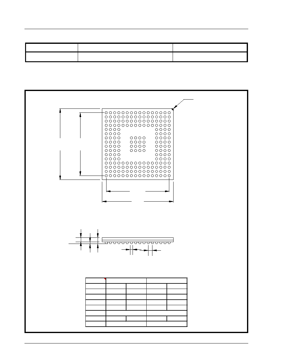
XRT79L71
PRELIMINARY
·Á
·Á
·Á
·Á
REV. P1.0.3
1 - CHANNEL DS3/E3 ATM UNI/PPP COMBO IC
428
ORDERING INFORMATION
PACKAGE DIMENSIONS
P
RODUCT
N
UMBER
P
ACKAGE
T
YPE
O
PERATING
T
EMPERATURE
R
ANGE
XRT79L71IB
17X17 mm 208 Ball Shrink Thin Ball Grid Array
-40
0
C to +85
0
C
208 SHRINK THIN BALL GRID ARRAY (17.0 MM X 17.0 MM, STBGA)
D 1
D
J
(A 1 corne r fe atu re is m fg er op tio n)
S ea tin g
A 2
A 1
A
P la ne
b
e
D 1
D
N
R
T
P
L
M
K
A 1
F E A T U R E /M A R K
1 3
1 6 1 5 1 4
E
G
H
F
D
C
B
1 1
1 2
1 0
9
8
7
6
4
5
3
A
2
1
SYMBOL
MIN
MAX
MIN
MAX
A
0.047
0.067
1.20
1.70
A1
0.010
0.022
0.25
0.55
A2
0.031
0.043
0.80
1.10
D
0.661
0.677
16.80
17.20
D1
0.591 BSC
15.00 BSC
b
0.018
0.022
0.45
0.55
e
0.0394 BSC
1.00 BSC
INCHES
MILLIMETERS
Note: The control dimension is in millimeter.

XRT79L71
PRELIMINARY
·Á
·Á
·Á
·Á
REV. P1.0.3
1 - CHANNEL DS3/E3 ATM UNI/PPP COMBO IC
429
NOTICE
EXAR Corporation reserves the right to make changes to the products contained in this publication in order to
improve design, performance or reliability. EXAR Corporation assumes no responsibility for the use of any
circuits described herein, conveys no license under any patent or other right, and makes no representation that
the circuits are free of patent infringement. Charts and schedules contained here in are only for illustration
purposes and may vary depending upon a user's specific application. While the information in this publication
has been carefully checked; no responsibility, however, is assumed for inaccuracies.
EXAR Corporation does not recommend the use of any of its products in life support applications where the
failure or malfunction of the product can reasonably be expected to cause failure of the life support system or to
significantly affect its safety or effectiveness. Products are not authorized for use in such applications unless
EXAR Corporation receives, in writing, assurances to its satisfaction that: (a) the risk of injury or damage has
been minimized; (b) the user assumes all such risks; (c) potential liability of EXAR Corporation is adequately
protected under the circumstances.
Copyright 2003 EXAR Corporation
Datasheet June 2003.
Reproduction, in part or whole, without the prior written consent of EXAR Corporation is prohibited.
REVISION HISTORY
R
EVISION
#
D
ATE
D
ESCRIPTION
P1.0.0
07/18/02
1st release of the XRT99L00 mkll.0
preliminary data sheet.
P1.0.1
02/12/03
Added package outline and pin-out diagram.
P1.0.2
05/03
Added Pin Descriptions
P1.0.3
06/03
Added Electrical Specifications and Register Information.