 | –≠–ª–µ–∫—Ç—Ä–æ–Ω–Ω—ã–π –∫–æ–º–ø–æ–Ω–µ–Ω—Ç: XRT8001IP | –°–∫–∞—á–∞—Ç—å:  PDF PDF  ZIP ZIP |

EXAR Corporation, 48720 Kato Road, Fremont, CA 94538
∑
(510) 668-7000
∑
FAX (510) 668-7017
∑
www.exar.com
Rev. 1.01
XRT8001
WAN Clock for T1 and E1 Systems
October 2001-1
GENERAL DESCRIPTION
The XRT8001 WAN Clock is a dual-phase-locked loop
chip that generates two very low jitter output clock
signals that can be used for synchronization clocks in
wide area networking systems. The XRT8001 has pre-
programmed multipliers and dividers that are selected
via the serial port. It generates two integer multiples of
8kHz, 56kHz, and 64kHz while locked onto an incom-
ing reference of 1.54MHz (T1), 2.048MHz (E1), 8kHz,
56kHz, or 64kHz
The XRT8001 WAN Clock can be configured to oper-
ate in one of six modes:
1.
The Forward/Master Mode
2.
The Reverse/Master Mode
3.
The "Fractional T1/E1" Reverse/Master Mode
4.
The "E1 to T1 - Forward/Master" Mode
5.
The "High Speed - Reverse" Mode
6.
The "Slave" Mode
FEATURES
∑
Dual Phased Locked Loops with
Pre-Programmed Multipliers and Dividers
∑
Pre-Programmed with Popular Frequency
Conversions for Communications Systems
Part Number
Package
Operating Temperature Range
XRT8001IP
18-Lead 300 Mil PDIP
-40
∞
C to +85
∞
C
XRT8001ID
18-Lead 300 Mil JEDEC SOIC
-40
∞
C to +85
∞
C
ORDERING INFORMATION
Reference Clock
8kHz to 16.384 MHz
Sync Out
8kHz or 64kHz
Master/Slave
Clock Output 1
Clock Output 2
PLL Lock Detect
µ
µ
C
/
µ
µ
P Serial I/O
F
IN
SYNC
MSB
CLK1
CLK2
LOCKDET
XRT8001
3
2
8
6
13
11
SCLK
SDI
SDO
CS
3.3V or 5V
CC
V
Figure 1. System Diagram
∑
Generates Output Clock Frequencies Ranging
From 8kHz up to 16.384MHz
∑
Serial Port Control for Optimal Performance
∑
Sync Output: 8kHz or 64kHz
∑
Low Jitter
∑
Cascadable (Master / Slave Modes)
∑
No External Components Needed
∑
Pin Compatible with the XRT8000
∑
Low Power (3.3V or 5V): 40 - 100mW
∑
- 40∞C to +85∞C Temperature Range
∑
18-Lead PDIP or SOIC Packages
APPLICATIONS
∑
T1/E1 Access Equipment (DSU/CSU)
∑
Frame Relay Access Devices (FRAD)
∑
Basic Rate and Primary Rate ISDN Equipment
∑
ISDN Routers
∑
Terminals
∑
Remote Access Servers
∑
T1/E1 Concentrators
∑
T1/E1 Multiplexers
∑
T1/E1 Clock Rate Converters
∑
Internal Timing Generators
∑
System Synchronizers
XRT8001
2
Rev. 1.01
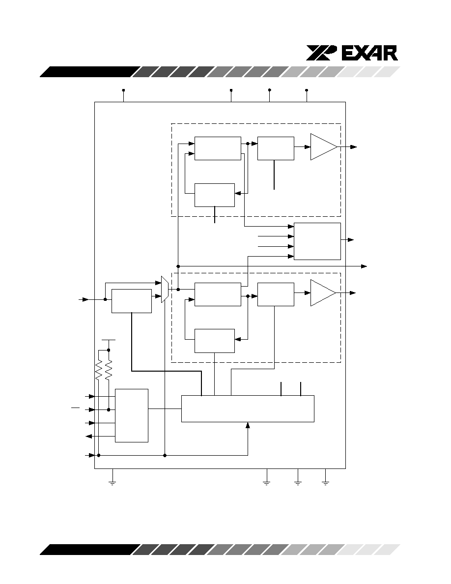
Figure 2. XRT8001 Block Diagram
F
IN
MSB
SCLK
CS
LOCKDET
SDO
R
100K
Vcc
SDI
Lock
Detector
Serial
Interface
Input
Divider
Mode and Frequency Select Control
Analog
Phase Locked
Loop
Post
Divider
Driver
Feedback
Divider
Driver
M2
Q2
M2
Q2
Analog
Phase Locked
Loop
Feedback
Divider
PLL2
CLK2
CLK1
SYNC
PLL1
P
R
100K
M
Q
M
Post
Divider
Q
LDETDIS1
LDETDIS2
Analog Vcc
Digital Vcc
15
Digital Vcc
7
10
13
11
2
6
14
5
D
GND
D
GND
9
A
GND
8
1
16
17
18
3
Digital Vcc
12
4
D
GND

XRT8001
3
Rev. 1.01
1
2
3
4
5
6
7
9
8
10
11
12
13
14
15
16
18
17
XRT8001
SDO
SYNC
FIN
GND
GND
CLK1
VCC
MSB
GND
VCC
LOCKDET
VCC
CLK2
GND
VCC
SDI
CS
SCLK
Figure 3. XRT8001 PIN OUT
PIN DESCRIPTION
Pin #
Name
Type
Description
1
SDO
O
Serial Data Output from the Microprocessor Serial Interface
This pin will serially output the contents of the specified Command
Register, during "Read" Operations. The data, on this pin, will be
updated on the falling edge of the SCLK input signal. This pin will be tri-
stated upon completion of data transfer.
2
SYNC
O
Sync Output - The XRT8001 will typically output an 8kHz clock signal
via this output pin.
However, when the XRT8001 is operating in the "High Speed - Reverse"
Mode, then this device will simply output a 64kHz clock signal.
3
FIN
I
Reference Clock Input - The Reference Timing signal (from which the
CLK1 and CLK2 output signals are derived) is to be input via this pin.
4
GND
-
Digital Ground
5
GND
-
Digital Ground
6
CLK1
O
Clock Output 1 - The XRT8001 will drive the desired "synthesized"
signal via this output pin. This output signal will have a 50+5% duty
cycle.
Note: This output pin is tri-stated unless the "CLK1EN" bit-field (within
Command Register CR4) has been set to "1".
7
V
CC
-
Digital Power Supply

XRT8001
4
Rev. 1.01
PIN DESCRIPTION (CONT'D)
Pin #
Name
Type
Description
8
MSB
I
Master/Slave Mode Select Input - Setting this input pin "HIGH"
configures the XRT8001 to operate in the "MASTER" Mode. Conversely,
setting this input pin "LOW" configures the XRT8001 to operate in the
"SLAVE" Mode.
9
GND
-
Analog Ground
10
VCC
-
Analog Power Supply
11
LOCKDET
O
Lock Detect Output - This output indicates whether or not the "selected"
internal PLL(s) are "in-lock" or are "out-of-lock".
By default, this output pin is "high" when both PLLs are in-lock" and will
go toggle "low" if either one of the PLLs is "out-of-lock".
However, the XRT8001 also permits the user to configure this output pin
to reflect the state of any one of the PLLs within the chip. (See Table 3.)
12
VCC
-
Digital Power Supply
13
CLK2
O
Clock Output 2 - The XRT8001 will drive the desired "synthesized"
signal via this output pin. This output signal will have a 50+5% duty
cycle.
Note: This output pin is tri-stated unless the "CLK1EN" bit-field (within
Command Register CR4) has been set to "1".
14
GND
-
Digital Ground
15
VCC
-
Digital Power Supply
16
SDI
I
Microprocessor Serial Interface ≠ Serial Data Input
Whenever, the user wishes to read or write data into the Command
Registers, over the Microprocessor Serial Interface, the user is expected
to apply the "Read/Write" bit, the Address Values (of the Command
Registers) and Data Value to be written (during "Write" Operations) to
this pin.
This input will be sampled on the rising edge of the SCLK pin (pin 18).
17
CS
I
Microprocessor Serial Interface ≠ Chip Select Input:
The Local Microprocessor must assert this pin (e.g., set it to "0") in order
to enable communication with the XRT8001 via the Microprocessor
Serial Interface.
Note: This pin is internally pulled "high".
18
SCLK
I
Microprocessor Serial Interface-Clock Signal
This signal will be used to sample the data, on the SDI pin, on the rising
edge of this signal. Additionally, during "Read" operations, the
Microprocessor Serial Interface will update the SDO output on the falling
edge of this signal.

XRT8001
5
Rev. 1.01
Symbol
Parameter
Min.
Typ.
Max. Units
Condition
V
IL
Input Low Level
0.8
V
V
IH
Input High Level
2.0
V
V
OL
Output Low Level (CLK1, CLK2)
0.4
V
I
OL
= -6.0mA
V
OH
Output High Level (CLK1, CLK2)
2.4
V
I
OL
= 6.0mA
V
OL
Output Low Level (LOCKDET, SYNC)
0.4
V
I
OL
= -3.0mA
V
OH
Output High Level (LOCKDET, SYNC)
2.4
V
I
OL
= 3.0mA
I
IL
Input Low Current (CSB, MSB)
-150
mA
I
IH
Input High Current (CSB, MSB)
10
mA
V
IN
= V
CC
I
IL
Input Low Current (except CSB, MSB)
-10
mA
I
IH
Input High Current (except CSB, MSB)
10
mA
V
IN
= V
CC
I
CC
Operating Current
11
30
mA
3.3V, No Load, CLk1, CLK2 = 8 x 2.048MHz
20
35
mA
5V, No Load, CLk1, CLK2 = 8 x 2.048MHz
R
IN
Internal Pull-up Resistance (CSB, MSB)
50
100
150
kW
DC ELECTRICAL CHARACTERISTICS (Except Microprocessor Serial Interface)
1
ABSOLUTE MAXIMUM RATINGS
Supply Range ................................................ 7V
Voltage at any Pin ........... GND -0.3V to Vcc+0.3V
Operating Temperature................. - 40∞C to +85∞C
Storage Temperature ................... - 40∞C to +85∞C
Package Dissipation ............................... 500mW
Note:
1. 5V tolerant input considerations when operating from 3.3V:
When the XRT8001 is powered at 3.3V, it can tolerate 5V-level signals via its inputs. However, the user should be aware the XRT8001
contains a "Factory-Test" Mode. This mode is enabled whenever the MSB (Master-Slave select) input pin is pulled to about 2V above
VDD.
Therefore, if the user is powering the XRT8001 at 3.3V but is applying a 5.25V signal to the MSB input pin, then it is possible that the
XRT8001 could be configured to operate in this "Factory-Test" Mode. Since all "Factory-Test" Mode registers are reset to "0", upon
chip power, this should not be a problem for the user.
However, if the user performs write operations to "non-defined" address locations within the XRT8001, then the user may observe strange
operation from the XRT8001. The user must make sure that when the Microcontroller performs WRITE operations to the XRT8001, it
is only performing these WRITE operations to the Address Locations defined in the XRT8001 Data Sheet.