Exar
Corporation 48720 Kato Road, Fremont CA, 94538
∑
(510) 668-7000
∑
FAX (510) 668-7017
∑
www.exar.com
·Á
·Á
·Á
·Á
XRT82L24
QUAD E1 LINE TRANSCEIVER WITH CLOCK RECOVERY AND JITTER ATTENUATOR
MARCH 2003
REV. 1.2.3
GENERAL DESCRIPTION
The XRT82L24 is a fully integrated Quad (four chan-
nels) short-haul line interface unit for E1(2.048Mbps)
75
or 120
applications. Each channel consists of a
receiver with equalizer for reliable data and clock re-
covery, and a transmitter which accepts either single
or dual-rail digital inputs for signal transmission to the
line using a low output impedance line driver. The de-
vice also includes a crystal-less jitter attenuator
which, depending on system requirements, can be
selected in the receive or transmit path through the
Host or Hardware Mode control.
XRT82L24 is a low power CMOS device operating on
a single 3.3V supply with 5V tolerant digital inputs.
FEATURES
∑ Fully integrated quad, short-haul PCM transceivers
for E1 applications.
∑ On Chip Receive Equalizer and Transmit Pulse
Shaper for CEPT 75
and 120
line terminations
∑ On chip clock recovery circuit
∑ Transformer or capacitor coupled receiver inputs
∑ Crystal-less jitter attenuator can be selected in the
transmit or receive path
∑ High receiver interference immunity
∑ Per-channel transmit power shutdown
∑ Tri-state transmit output capability
∑ On chip per-channel driver failure monitoring circuit
∑ On chip HDB3/B8ZS/AMI encoder/decoder func-
tions
∑ Transmit return loss meets or exceeds ETSI 300
166 standard
∑ Meets or exceeds specifications in ITU G.703,
G.775, G.736 and G.823; ETSI 300-166
∑ 3.3V or 5.0V Logic level inputs
∑ Single +3.3V Supply Operation
∑ Same pin Out as XRT82L34 T1/E1/J1 LIU
∑ New Patent# 6,313,671B1 Low Power IC I/O Buffer
APPLICATIONS
∑ Digital cross connects (DSX-1)
∑ Channel Banks
∑ High speed data transmission line cards
∑ E1 Multiplexer
∑ Public switching systems and PBX interfaces
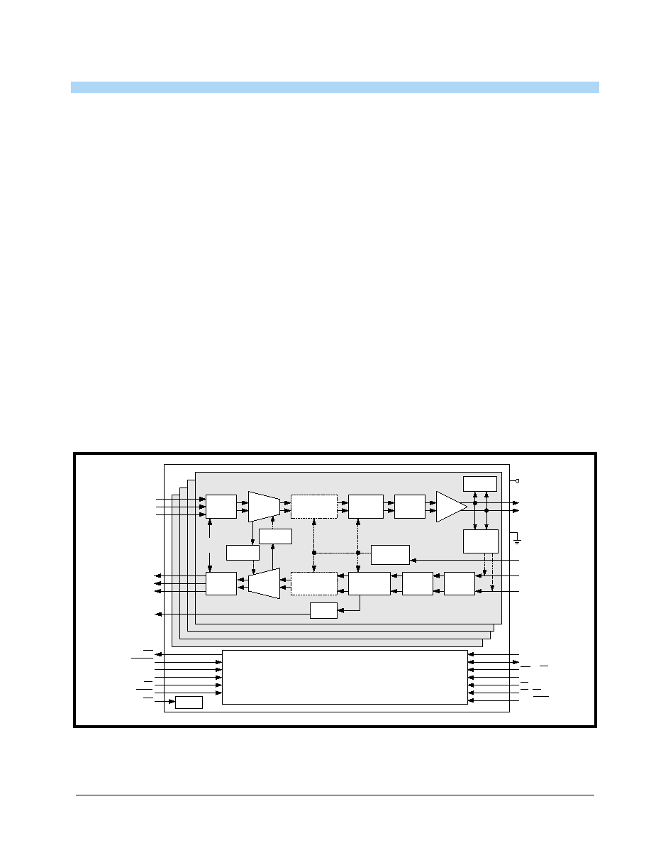
F
IGURE
1. B
LOCK
D
IAGRAM
OF
THE
XRT82L24 E1 LIU (H
OST
M
ODE
)
HDB3
Encoder
MUX
Tx/Rx Jitter
Attenuator
Tx Timing
Control
Tx Pulse
Shaper
MUX
Line
Driver
Tx/Rx Jitter
Attenuator
Timing & Data
Recovery
Peak
Detector
& Slicer
Rx
Equalizer
LOS
Detect
HDB3
Decoder
Clock
Generator
MClk
TVDD_n
TTIP_n
TRing_n
TGND_n
Enable/
Disable
RTIP_n
RRing_n
Remote
LoopBack
Local
Analog
LoopBack
Digital
LoopBack
Driver
Monitor
Channel 0
Channel 1
Channel 2
Channel 3
HW/HOST
µ
µ
µ
µ
P Controller & Hardware Interface
ADD [0:3]
D[0:7]
WR_R/W/TxOFF_0
ALE_AS/TxOFF_2
CS/TxOFF_3
RD_DS/TxOFF_1
Test
TxClk_n/RZData_n
TxPOS_n/TDATA_n
TxNEG_n
RxClk_n
RxPOS_n/RDATA_n
RxNEG_n/LCV_n
RxLOS_n
INT
RDY_DTACK
PClk/Codes
PTS1/ClkE
PTS2/SR_DR
Reset
ICT

XRT82L24
·Á
·Á
·Á
·Á
QUAD E1 LINE TRANSCEIVER WITH CLOCK RECOVERY AND JITTER ATTENUATOR
REV. 1.2.3
I
TABLE OF CONTENTS
GENERAL DESCRIPTION ................................................................................................. 1
F
EATURES
.................................................................................................................................................... 1
A
PPLICATIONS
.............................................................................................................................................. 1
Figure 1. Block Diagram of the XRT82L24 E1 LIU (Host Mode) ........................................................... 1
Figure 2. Block Diagram of the XRT82L24 T1/E1/J LIU (Hardware Mode) ........................................... 2
Figure 3. Pin Out of the XRT82L24 .......................................................................................................... 3
TABLE OF CONTENTS ....................................................................................................... I
PIN DESCRIPTION ............................................................................................................. 4
R
ECEIVER
S
ECTIONS
.................................................................................................................................... 4
T
RANSMITTER
S
ECTIONS
.............................................................................................................................. 4
M
ICROPROCESSOR
I
NTERFACE
...................................................................................................................... 5
C
LOCKS
....................................................................................................................................................... 7
J
ITTER
A
TTENUATOR
.................................................................................................................................... 7
C
ONTROL
..................................................................................................................................................... 7
P
OWER
S
UPPLIES
AND
G
ROUNDS
................................................................................................................. 8
SYSTEM-FUNCTIONAL DESCRIPTION ......................................................................... 10
R
ECEIVER
.................................................................................................................................................. 10
J
ITTER
A
TTENUATOR
.................................................................................................................................. 10
HDB3/AMI D
ECODER
................................................................................................................................. 10
R
ECEIVER
L
OSS
OF
S
IGNAL
(LOS) .............................................................................................................. 10
C
ONDITIONS
FOR
DECLARING
AND
CLEARING
LOS
IN
THE
E1 M
ODE
. ............................................................ 11
R
ECEIVE
D
ATA
M
UTING
.............................................................................................................................. 11
LOOP-BACK MODES .............................................................................................................................. 11
R
EMOTE
L
OOP
-B
ACK
(RLOOP) MODE ...................................................................................................... 11
D
IGITAL
L
OCAL
LOOP
-B
ACK
(DLOOP)
MODE
............................................................................................... 11
A
NALOG
LOCAL
L
OOP
-B
ACK
(ALOOP)
MODE
.............................................................................................. 11
Figure 4. Remote Loop-Back with jitter attenuator selected in receive path .................................... 12
Figure 5. Remote Loop-Back with jitter attenuator selected in transmit path .................................. 12
Figure 6. Digital Local Loop-Back with option to transmit all "ones" to the line (JA selected & in re-
ceive path) .............................................................................................................................. 13
Figure 7. Digital Local Loop-Back with option to transmit all "ones" to the line (JA selected & in
transmit path) ......................................................................................................................... 13
Figure 8. Analog Local Loop-Back signal flow Jitter Attenuator selected & in Receive path ........ 14
Figure 9. Analog Local Loop-Back signal flow Jitter Attenuator selected & in transmit path ........ 14
R
ESET
O
PERATION
..................................................................................................................................... 14
R
ECEIVER
M
ODES
OF
O
PERATION
............................................................................................................... 14
R
ECEIVE
D
ATA
I
NVERT
M
ODE
..................................................................................................................... 14
Figure 10. Data changes on rising edge of Clk and Data is sampled on falling edge ..................... 15
Figure 11. Data changes on falling edge of Clk and is sampled on rising edge .............................. 15
T
RANSMIT
C
LOCK
S
AMPLING
E
DGE
............................................................................................................. 15
SINGLE
RAIL
, D
UAL
RAIL
.............................................................................................................................. 15
T
RANSMIT
A
LL
O
NES
(TAOS) ..................................................................................................................... 15
HDB3/AMI E
NCODER
................................................................................................................................. 15
T
RANSMIT
P
ULSE
S
HAPER
.......................................................................................................................... 16
D
RIVER
M
ONITOR
....................................................................................................................................... 16
TRANSMIT
OFF
CONTROL
............................................................................................................................ 16
I
NTERFACING
THE
XRT 82L24
TO
THE
L
INE
................................................................................................ 16
Figure 12. XRT 82L24 Channel 1in an E1 unbalanced 75 W application ........................................... 16
Figure 13. XRT 82L24 Channel 1 - E1 120 W balanced application ................................................... 17
T
ABLE
1: E1 R
ECEIVER
E
LECTRICAL
C
HARACTERISTICS
............................................................................. 18
T
ABLE
2: E1 T
RANSMITTER
E
LECTRICAL
C
HARACTERISTICS
....................................................................... 19
T
ABLE
3: T
RANSMIT
P
ULSE
M
ASK
S
PECIFICATION
...................................................................................... 19

·Á
·Á
·Á
·Á
XRT82L24
QUAD E1 LINE TRANSCEIVER WITH CLOCK RECOVERY AND JITTER ATTENUATOR
REV. 1.2.3
II
Figure 14. ITU G.703 E1 Pulse Template .............................................................................................. 20
T
ABLE
4: DC E
LECTRICAL
C
HARACTERISTICS
............................................................................................ 20
T
ABLE
5: P
OWER
C
ONSUMPTION
(T
A
=-40∞C
TO
85∞C, V
DD
=3.3V + 5%,
UNLESS
OTHERWISE
SPECIFIED
.) .. 21
ABSOLUTE MAXIMUM RATINGS ................................................................................... 21
T
ABLE
6: AC E
LECTRICAL
C
HARACTERISTICS
............................................................................................ 21
Figure 15. Transmit Clock and Input Data Timing .............................................................................. 22
Figure 16. Receive Clock and Output Data Timing. ............................................................................ 23
T
ABLE
7: M
ICROPROCESSOR
INTERFACE
SIGNAL
........................................................................................ 24
T
ABLE
8: M
ICROPROCESSOR
R
EGISTER
M
AP
............................................................................................. 25
T
ABLE
9: C
OMMAND
C
ONTROL
R
EGISTER
0 ............................................................................................... 26
T
ABLE
10: C
OMMAND
C
ONTROL
R
EGISTER
1 ............................................................................................. 27
T
ABLE
11: C
HANNEL
S
TATUS
R
EGISTER
.................................................................................................... 28
T
ABLE
12: C
HANNEL
M
ASK
R
EGISTER
....................................................................................................... 29
T
ABLE
13: C
HANNEL
C
ONTROL
R
EGISTER
................................................................................................ 30
Figure 17. Intel Interface Timing (Read) ............................................................................................... 31
Figure 18. Intel Interface Timing (Write) ............................................................................................... 31
T
ABLE
14: I
NTEL
I
NTERFACE
T
IMING
S
PECIFICATIONS
................................................................................. 32
Figure 19. Microprocessor Interface Timing - Motorola Type Programmed I/O Read Operation ... 33
Figure 20. Microprocessor Interface Timing - Motorola Type Programmed I/O Write Operation ... 33
Figure 21. Microprocessor Interface Timing - Reset Pulse Width ..................................................... 34
T
ABLE
15: M
OTOROLA
I
NTERFACE
T
IMING
S
PECIFICATION
.......................................................................... 34
J
ITTER
T
OLERANCE
.................................................................................................................................... 35
Figure 22. Receive Maximum Jitter Tolerance .................................................................................... 35
Figure 23. Receiver Jitter Transfer Function (Jitter Attenuator disabled) ........................................ 36
Figure 24. Jitter Attenuation Function ................................................................................................. 36
APPENDIX A ..................................................................................................................... 37
XRT82LL34
AND
XRT82L24 E
VALUATION
K
IT
(XRT82L34/L24EVAL) ...................................................... 37
Figure 25. XRT82L34/L24 GUI Software Interface for Evaluating the XRT82L24/L34EVAL Application
Board ...................................................................................................................................... 37
Figure 26. Photograph of the XRT82L34/L24EVAL Application Board ............................................. 38
Figure 27. Block Layout of the XRT82L34/L24EVAL Application Board ........................................... 39
O
RDERING
I
NFORMATION
............................................................................................................................ 40
P
ACKAGE
D
IMENSIONS
100 L
EAD
TQFP 14
X
14
MM
..................................................................................... 40
R
EVISION
H
ISTORY
..................................................................................................................................... 41

