Exar
Corporation 48720 Kato Road, Fremont CA, 94538
∑
(510) 668-7000
∑
FAX (510) 668-7017
∑
www.exar.com
·Á
·Á
·Á
·Á
PRELIMINARY
XRT83L30
SINGLE-CHANNEL T1/E1/J1 LH/SH TRANSCEIVER WITH CLOCK RECOVERY AND JITTER ATTENUATOR
MAY 2003
REV. P1.3.0
GENERAL DESCRIPTION
The XRT83L30 is a fully integrated single-channel
long-haul and short-haul line interface unit for
T1(1.544Mbps) 100
, E1(2.048Mbps) 75
or 120
and J1 110
applications.
In long-haul applications the XRT83L30 accepts sig-
nals that have passed through cables from 0 feet to
over 6000 feet in length and have been attenuated by
0 to 45dB at 772kHz in T1 mode or 0 to 43dB at
1024kHz in E1 mode. In T1 applications, the
XRT83L30 can generate five transmit pulse shapes to
meet the short-haul Digital Cross-Connect (DSX-1)
template requirements as well as for Channel Service
Units (CSU) Line Build Out (LBO) filters of 0dB,
-7.5dB, -15dB and -22.5dB as required by FCC rules.
It also provides programmable transmit pulse genera-
tor that can be used for arbitrary output pulse shaping
allowing performance improvement over a wide vari-
ety of conditions.
The XRT83L30 provides both Serial Host micropro-
cessor interface and Hardware Mode for program-
ming and control. Both B8ZS and HDB3 encoding
and decoding functions are included and can be dis-
abled as required. On-chip crystal-less jitter attenua-
tor with a 32 or 64 bit FIFO can be placed either in the
receive or the transmit path with loop bandwidths of
less than 3Hz. The XRT83L30 provides a variety of
loop-back and diagnostic features as well as transmit
driver short circuit detection and receive loss of signal
monitoring. It supports internal impedance matching
for 75
,
100
,
110
and 120
for both transmitter
and receiver. For the receiver this is accomplished by
internal resistors or through the combination of one
single fixed value external resistor and programmable
internal resistors. In the absence of the power supply,
the transmit output and receive input are tri-stated al-
lowing for redundancy applications. The chip includes
an integrated programmable clock multiplier that can
synthesize T1 or E1 master clocks from a variety of
external clock sources.
APPLICATIONS
∑ T1 Digital Cross-Connects (DSX-1)
∑ ISDN Primary Rate Interface
∑ CSU/DSU E1/T1/J1 Interface
∑ T1/E1/J1 LAN/WAN Routers
∑ Public switching Systems and PBX Interfaces
∑ T1/E1/J1 Multiplexer and Channel Banks
FEATURES
(See Page 2)
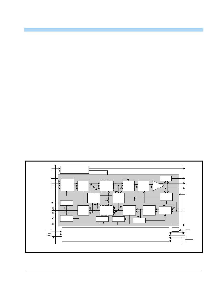
F
IGURE
1. B
LOCK
D
IAGRAM
OF
THE
XRT83L30 T1/E1/J1 LIU (H
OST
M
ODE
)
HW/HOST
CS
INT
ICT
TXTEST[0:2]
INSBPV
TPOS / TDATA
TNEG / CODES
TCLK
QRPD
RCLK
RNEG / LCV
RPOS / RDATA
NLCD
RLOS
RTIP
RRING
MASTER CLOCK SYNTHESIZER
QRSS
PATTERN
GENERATOR
DMO
TTIP
TRING
TXON
HDB3/
B8ZS
ENCODER
TX/RX JITTER
ATTENUATOR
TIMING
CONTROL
TX FILTER
& PULSE
SHAPER
LINE
DRIVER
DRIVE
MONITOR
LOCAL
ANALOG
LOOPBACK
REMOTE
LOOPBACK
DIGITAL
LOOPBACK
HDB3/
B8ZS
DECODER
TX/RX JITTER
ATTENUATOR
TIMING &
DATA
RECOVERY
PEAK
DETECTOR
& SLICER
QRSS
DETECTOR
NETWORK
LOOP
DETECTOR
RX
EQUALIZER
EQUALIZER
CONTROL
AIS
DETECTOR
LOS
DETECTOR
LBO[3:0]
LOOPBACK
ENABLE
JA
SELECT
NLCD ENABLE
QRSS ENABLE
SDO
SCLK
SDI
RESET
Serial Interface
TEST
TAOS
ENABLE
MCLKE1
MCLKT1
MCLKOUT
AISD
XRT83L30
·Á
·Á
·Á
·Á
SINGLE-CHANNEL T1/E1/J1 LH/SH TRANSCEIVER WITH CLOCK RECOVERY AND JITTER ATTENUATOR
REV. P1.3.0
PRELIMINARY
2
FEATURES
∑ Fully integrated single-channel long-haul and short-
haul transceiver for E1,T1 or J1 applications.
∑ Adaptive Receive Equalizer for cable attenuation of
up to 45dB for T1 and 43dB for E1.
∑ Programmable Transmit Pulse Shaper for E1,T1 or
J1 short-haul interfaces.
∑ Five fixed transmit pulse settings for T1 short-haul
applications plus a fully programmable waveform
generator for transmit output pulse shaping.
∑ Programmable Transmit Line Build-Outs (LBO) for
T1 long-haul application from 0dB to -22.5dB in
three 7.5dB steps.
∑ Tri-State transmit output and receive input capabil-
ity for redundancy applications
∑ Selectable receiver sensitivity from 0 to 36dB or 0
to 45dB cable loss for T1 @772kHz and 0 to 43dB
for E1 @1024kHz.
∑ High receiver interference immunity
∑ Receive monitor mode handles 0 to 29dB resistive
attenuation along with 0 to 6dB of cable attenuation
for both T1 and E1 modes.
∑ Supports 75
and 120
(E1), 100
(T1) and 110
(J1) applications.
∑ Internal and external impedance matching for
75
,100
,
110
and 120
.
∑ Transmit return loss meets or exceeds ETSI 300
166 standard
∑ On-chip digital clock recovery circuit for high input
jitter tolerance
∑ Crystal-less digital jitter attenuator with 32-bit or 64-
bit FIFO Selectable either in transmit or receive
path
∑ On-chip frequency multiplier generates T1 or E1
Master clocks from variety of external clock sources
∑ On-chip transmit short-circuit protection and limit-
ing, and driver fail monitor output (DMO)
∑ Receive loss of signal (RLOS) output
∑ On-chip HDB3/B8ZS/AMI encoder/decoder
∑ QRSS pattern generation and detection for testing
and monitoring
∑ Error and Bipolar Violation Insertion and Detection
∑ Receiver Line Attenuation Indication Output in 1dB
steps
∑ Network Loop-Code Detection for automatic Loop-
Back Activation/Deactivation
∑ Transmit All Ones (TAOS) and In-Band Network
Loop Up and Down code generators
∑ Supports Analog, Remote, Digital and Dual Loop-
Back Modes
∑ Meets or exceeds T1 and E1 short-haul and long-
haul network access specifications in ITU G.703,
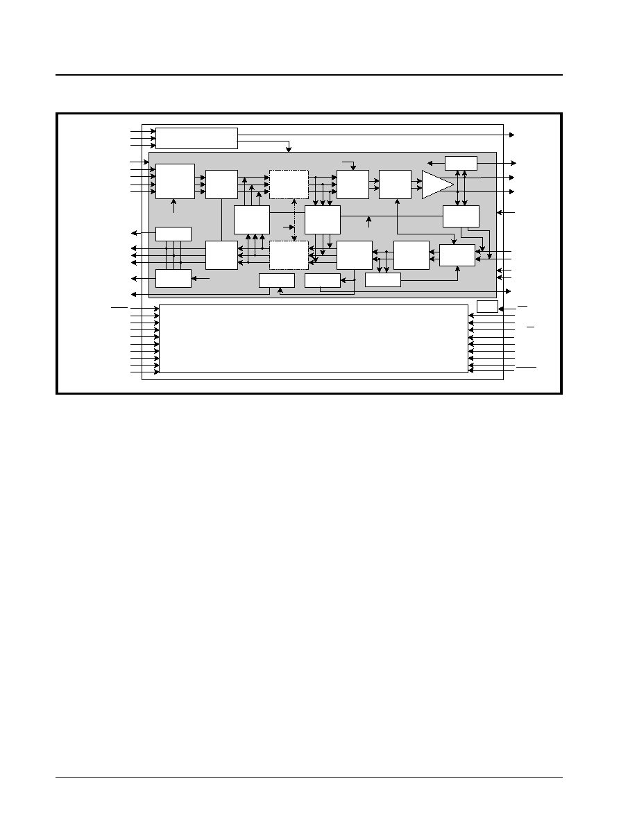
F
IGURE
2. B
LOCK
D
IAGRAM
OF
THE
XRT83L30 T1/E1/J1 LIU (H
ARDWARE
M
ODE
)
HW/HOST
GAUGE
JASEL1
JASEL0
RXTSEL
TXTSEL
TERSEL1
TERSEL0
RXRES1
RXRES0
ICT
MCLKE1
MCLKT1
CLKSEL[2:0]
TXTEST[0:2]
INSBPV
TPOS / TDATA
TNEG / CODES
TCLK
QRPD
RCLK
RNEG / LCV
RPOS / RDATA
NLCD
RLOS
RTIP
RRING
MASTER CLOCK SYNTHESIZER
QRSS
PATTERN
GENERATOR
DMO
TTIP
TRING
TXON
HDB3/
B8ZS
ENCODER
TX/RX JITTER
ATTENUATOR
TIMING
CONTROL
TX FILTER
& PULSE
SHAPER
LINE
DRIVER
LOCAL
ANALOG
LOOPBACK
REMOTE
LOOPBACK
DIGITAL
LOOPBACK
HDB3/
B8ZS
DECODER
TX/RX JITTER
ATTENUATOR
TIMING &
DATA
RECOVERY
PEAK
DETECTOR
& SLICER
QRSS
DETECTOR
NETWORK
LOOP
DETECTOR
RX
EQUALIZER
EQUALIZER
CONTROL
AIS
DETECTOR
LOS
DETECTOR
LBO[3:0]
LOOPBACK
ENABLE
JA
SELECT
NLCD ENABLE
QRSS ENABLE
HARWARE CONTROL
TEST
JABW
TRATIO
SR/DR
EQC[4:0]
TCLKE
RCLKE
RXMUTE
ATAOS
DRIVE
MONITOR
DFM
MCLKOUT
LOOP1
LOOP0
AISD
RESET
TAOS
ENABLE
·Á
·Á
·Á
·Á
XRT83L30
SINGLE-CHANNEL T1/E1/J1 LH/SH TRANSCEIVER WITH CLOCK RECOVERY AND JITTER ATTENUATOR
PRELIMINARY
REV. P1.3.0
3
G.775, G.736 and G.823; TR-TSY-000499; ANSI
T1.403 and T1.408; ETSI 300-166 and AT&T Pub
62411
∑ Supports both Hardware and serial Microprocessor
interface for programming
∑ Programmable Interrupt
∑ Low power dissipation
∑ Logic inputs accept either 3.3V or 5V levels
∑ Single +3.3V Supply Operation
∑ 64 pin TQFP package
∑ -40∞C to +85∞C Temperature Range
ORDERING INFORMATION
P
ART
N
UMBER
P
ACKAGE
O
PERATING
T
EMPERATURE
R
ANGE
XRT83L30IV
64 Lead TQFP (14 x 20 x 1.4mm)
-40
∞
C to +85
∞
C
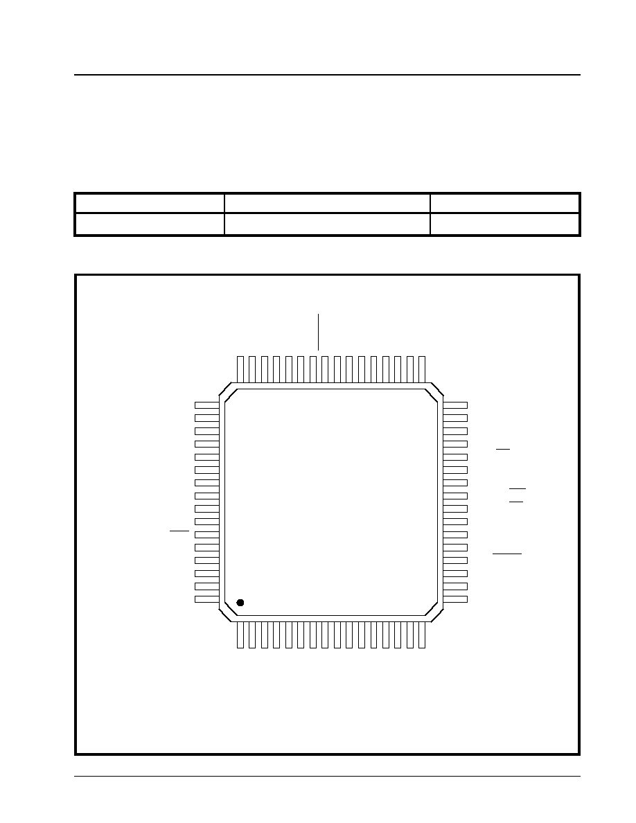
F
IGURE
3. P
IN
O
UT
OF
THE
XRT83L30
XRT83L30
1
2
3
4
5
6
7
8
9
10
11
12
13
14
15
16
R
N
E
G
/
L
C
V
RP
O
S
/
RDA
T
A
RA
VDD
RTI
P
RR
I
N
G
RA
G
N
D
TA
G
N
D
TTIP
TA
V
D
D
TR
I
N
G
DM
O
VD
DPLL
MC
L
K
E
1
MC
L
K
T
1
GND
P
L
L
MC
L
K
O
U
T
AGND
AVDD
LOOP0
LOOP1
SR / DR
ATAOS
TRATIO
EQC0 / INT
EQC1 / CS
EQC2 / SCLK
EQC3 / SDO
EQC4 / SDI
HW /HOST
CLKSEL0
CLKSEL1
CLKSEL2
JA
S
E
L0
JA
S
E
L1
JA
B
W
T
X
TSEL
RX
TSE
L
TE
R
S
E
L
1
TE
R
S
E
L
0
RE
SE
T
QRP
D
AI
SD
NL
CD
DG
ND
DV
DD
I
N
SBP
V
NL
CDE
0
NL
CDE
1
GAUGE
RXMUTE
RXRES1
RXRES0
RCLKE
TXTEST2
TXTEST1
TXTEST0
TCLKE
TXON
ICT
TCLK
TPOS / TDATA
TNEG / CODES
RLOS
RCLK
48
47
46
45
44
43
42
41
40
39
38
37
36
35
34
33
32
31
30
29
28
27
26
25
24
23
22
21
20
19
18
17
49
50
51
52
53
54
55
56
57
58
59
60
61
62
63
64

XRT83L30
·Á
·Á
·Á
·Á
SINGLE-CHANNEL T1/E1/J1 LH/SH TRANSCEIVER WITH CLOCK RECOVERY AND JITTER ATTENUATOR
REV. P1.3.0
PRELIMINARY
I
TABLE OF CONTENTS
GENERAL DESCRIPTION ................................................................................................. 1
A
PPLICATIONS
.............................................................................................................................................. 1
F
EATURES
.................................................................................................................................................... 1
Figure 1. Block Diagram of the XRT83L30 T1/E1/J1 LIU (Host Mode) ................................................. 1
Figure 2. Block Diagram of the XRT83L30 T1/E1/J1 LIU (Hardware Mode) ......................................... 2
F
EATURES
.................................................................................................................................................... 2
ORDERING INFORMATION ............................................................................................................... 3
Figure 3. Pin Out of the XRT83L30 .......................................................................................................... 3
TABLE OF CONTENTS ....................................................................................................... I
PIN DESCRIPTIONS BY FUNCTION ................................................................................. 4
S
ERIAL
I
NTERFACE
....................................................................................................................................... 4
R
ECEIVER
.................................................................................................................................................... 4
T
RANSMITTER
............................................................................................................................................... 6
J
ITTER
A
TTENUATOR
.................................................................................................................................... 8
C
LOCK
S
YNTHESIZER
.................................................................................................................................... 9
R
EDUNDANCY
SUPPORT
.............................................................................................................................. 11
T
ERMINATIONS
........................................................................................................................................... 11
C
ONTROL
FUNCTION
................................................................................................................................... 13
A
LARM
F
UNCTION
/O
THER
........................................................................................................................... 14
P
OWER
AND
GROUND
................................................................................................................................. 16
FUNCTIONAL DESCRIPTION ......................................................................................... 17
M
ASTER
C
LOCK
G
ENERATOR
...................................................................................................................... 17
Figure 4. Two Input Clock Source ......................................................................................................... 17
Figure 5. One Input Clock Source ......................................................................................................... 17
RECEIVER ........................................................................................................................ 18
R
ECEIVER
I
NPUT
......................................................................................................................................... 18
T
ABLE
1: M
ASTER
C
LOCK
G
ENERATOR
...................................................................................................... 18
R
ECEIVE
M
ONITOR
M
ODE
........................................................................................................................... 19
R
ECEIVER
L
OSS
OF
S
IGNAL
(RLOS) ........................................................................................................... 19
Figure 6. Simplified Diagram of -15dB T1/E1 Short Haul Mode and RLOS Condition ..................... 19
Figure 7. Simplified Diagram of -29dB T1/E1 Gain Mode and RLOS Condition ............................... 20
Figure 8. Simplified Diagram of -36dB T1/E1 Long Haul Mode and RLOS Condition ...................... 20
R
ECEIVE
HDB3/B8ZS D
ECODER
................................................................................................................ 21
R
ECOVERED
C
LOCK
(RCLK) S
AMPLING
E
DGE
............................................................................................ 21
Figure 9. Simplified Diagram of Extended RLOS mode (E1 Only) ..................................................... 21
Figure 10. Receive Clock and Output Data Timing ............................................................................. 21
J
ITTER
A
TTENUATOR
.................................................................................................................................. 22
G
APPED
C
LOCK
(JA M
UST
BE
E
NABLED
IN
THE
T
RANSMIT
P
ATH
) ................................................................. 22
T
ABLE
2: M
AXIMUM
G
AP
W
IDTH
FOR
M
ULTIPLEXER
/M
APPER
A
PPLICATIONS
............................................... 22
A
RBITRARY
P
ULSE
G
ENERATOR
.................................................................................................................. 23
TRANSMITTER ................................................................................................................. 23
D
IGITAL
D
ATA
F
ORMAT
............................................................................................................................... 23
T
RANSMIT
C
LOCK
(TCLK) S
AMPLING
E
DGE
................................................................................................ 23
Figure 11. Arbitrary Pulse Segment Assignment ................................................................................ 23
T
RANSMIT
HDB3/B8ZS E
NCODER
.............................................................................................................. 24
Figure 12. Transmit Clock and Input Data Timing ............................................................................... 24
T
ABLE
3: E
XAMPLES
OF
HDB3 E
NCODING
................................................................................................. 24
T
ABLE
4: E
XAMPLES
OF
B8ZS E
NCODING
.................................................................................................. 24
D
RIVER
F
AILURE
M
ONITOR
(DMO) .............................................................................................................. 25
T
RANSMIT
P
ULSE
S
HAPER
& L
INE
B
UILD
O
UT
(LBO)
CIRCUIT
...................................................................... 25
T
ABLE
5: R
ECEIVE
E
QUALIZER
C
ONTROL
AND
T
RANSMIT
L
INE
B
UILD
-O
UT
S
ETTINGS
.................................. 25

·Á
·Á
·Á
·Á
XRT83L30
SINGLE-CHANNEL T1/E1/J1 LH/SH TRANSCEIVER WITH CLOCK RECOVERY AND JITTER ATTENUATOR
PRELIMINARY
REV. P1.3.0
II
TRANSMIT AND RECEIVE TERMINATIONS .................................................................. 27
RECEIVER ............................................................................................................................................... 27
Internal Receive Termination Mode ................................................................................................................. 27
T
ABLE
6: R
ECEIVE
T
ERMINATION
C
ONTROL
................................................................................................ 27
Figure 13. Simplified Diagram for the Internal Receive and Transmit Termination Mode .............. 27
T
ABLE
7: R
ECEIVE
T
ERMINATIONS
............................................................................................................. 28
Figure 14. Simplified Diagram for T1 in the External Termination Mode (RXTSEL= 0) ................... 28
TRANSMITTER ........................................................................................................................................ 29
Transmit Termination Mode ............................................................................................................................. 29
External Transmit Termination Mode ............................................................................................................... 29
Figure 15. Simplified Diagram for E1 in External Termination Mode (RXTSEL= 0) ......................... 29
T
ABLE
8: T
RANSMIT
T
ERMINATION
C
ONTROL
............................................................................................. 29
T
ABLE
9: T
ERMINATION
S
ELECT
C
ONTROL
................................................................................................. 29
REDUNDANCY APPLICATIONS ............................................................................................................. 30
T
ABLE
10: T
RANSMIT
T
ERMINATION
C
ONTROL
........................................................................................... 30
T
ABLE
11: T
RANSMIT
T
ERMINATIONS
......................................................................................................... 30
TYPICAL REDUNDANCY SCHEMES ..................................................................................................... 31
Figure 16. Simplified Block Diagram of the Transmit Section for 1:1 & 1+1 Redundancy ............. 32
Figure 17. Simplified Block Diagram - Receive Section for 1:1 and 1+1 Redundancy .................... 32
Figure 18. Simplified Block Diagram - Transmit Section for N+1 Redundancy ............................... 33
Figure 19. Simplified Block Diagram - Receive Section for N+1 Redundancy ................................. 34
P
ATTERN
T
RANSMIT
AND
D
ETECT
F
UNCTION
............................................................................................... 35
T
RANSMIT
A
LL
O
NES
(TAOS) .................................................................................................................... 35
N
ETWORK
L
OOP
C
ODE
D
ETECTION
AND
T
RANSMISSION
.............................................................................. 35
T
ABLE
12: P
ATTERN
TRANSMISSION
CONTROL
............................................................................................ 35
T
RANSMIT
AND
D
ETECT
Q
UASI
-R
ANDOM
S
IGNAL
S
OURCE
(TDQRSS) ......................................................... 36
T
ABLE
13: L
OOP
-C
ODE
D
ETECTION
C
ONTROL
........................................................................................... 36
L
OOP
-B
ACK
M
ODES
................................................................................................................................... 38
L
OCAL
A
NALOG
L
OOP
-B
ACK
(ALOOP) ....................................................................................................... 38
T
ABLE
14: L
OOP
-
BACK
CONTROL
IN
H
ARDWARE
MODE
.............................................................................. 38
T
ABLE
15: L
OOP
-
BACK
CONTROL
IN
H
OST
MODE
........................................................................................ 38
Figure 20. Local Analog Loop-back signal flow .................................................................................. 38
R
EMOTE
L
OOP
-B
ACK
(RLOOP) ................................................................................................................. 39
Figure 21. Remote Loop-back mode with jitter attenuator selected in receive path ....................... 39
Figure 22. Remote Loop-back mode with jitter attenuator selected in Transmit path .................... 39
D
IGITAL
L
OOP
-B
ACK
(DLOOP) .................................................................................................................. 40
D
UAL
L
OOP
-B
ACK
...................................................................................................................................... 40
Figure 23. Digital Loop-back mode with jitter attenuator selected in Transmit path ...................... 40
Figure 24. Signal flow in Dual loop-back mode ................................................................................... 40
HOST MODE SERIAL INTERFACE OPERATION ........................................................... 41
U
SING
THE
M
ICROPROCESSOR
S
ERIAL
I
NTERFACE
...................................................................................... 41
Figure 25. Microprocessor Serial Interface Data Structure ................................................................ 42
T
ABLE
16: M
ICROPROCESSOR
R
EGISTER
A
DDRESS
................................................................................... 43
T
ABLE
17: M
ICROPROCESSOR
R
EGISTER
B
IT
M
AP
..................................................................................... 43
T
ABLE
18: M
ICROPROCESSOR
R
EGISTER
#0
BIT
DESCRIPTION
.................................................................... 45
T
ABLE
19: M
ICROPROCESSOR
R
EGISTER
#1
BIT
DESCRIPTION
.................................................................... 46
T
ABLE
20: M
ICROPROCESSOR
R
EGISTER
#2
BIT
DESCRIPTION
.................................................................... 48
T
ABLE
21: M
ICROPROCESSOR
R
EGISTER
#3
BIT
DESCRIPTION
.................................................................... 50
T
ABLE
22: M
ICROPROCESSOR
R
EGISTER
#4
BIT
DESCRIPTION
.................................................................... 52
T
ABLE
23: M
ICROPROCESSOR
R
EGISTER
#5
BIT
DESCRIPTION
.................................................................... 53
T
ABLE
24: M
ICROPROCESSOR
R
EGISTER
#6
BIT
DESCRIPTION
.................................................................... 55
T
ABLE
25: M
ICROPROCESSOR
R
EGISTER
#7
BIT
DESCRIPTION
.................................................................... 56
T
ABLE
26: M
ICROPROCESSOR
R
EGISTER
#8
BIT
DESCRIPTION
.................................................................... 56
T
ABLE
27: M
ICROPROCESSOR
R
EGISTER
#9
BIT
DESCRIPTION
.................................................................... 57

XRT83L30
·Á
·Á
·Á
·Á
SINGLE-CHANNEL T1/E1/J1 LH/SH TRANSCEIVER WITH CLOCK RECOVERY AND JITTER ATTENUATOR
REV. P1.3.0
PRELIMINARY
III
T
ABLE
28: M
ICROPROCESSOR
R
EGISTER
#10
BIT
DESCRIPTION
.................................................................. 57
T
ABLE
29: M
ICROPROCESSOR
R
EGISTER
#11
BIT
DESCRIPTION
.................................................................. 58
T
ABLE
30: M
ICROPROCESSOR
R
EGISTER
#12
BIT
DESCRIPTION
.................................................................. 58
T
ABLE
31: M
ICROPROCESSOR
R
EGISTER
#13
BIT
DESCRIPTION
.................................................................. 59
T
ABLE
32: M
ICROPROCESSOR
R
EGISTER
#14
BIT
DESCRIPTION
.................................................................. 59
T
ABLE
33: M
ICROPROCESSOR
R
EGISTER
#15
BIT
DESCRIPTION
.................................................................. 60
T
ABLE
34: M
ICROPROCESSOR
R
EGISTER
#16
BIT
DESCRIPTION
.................................................................. 61
T
ABLE
35: M
ICROPROCESSOR
R
EGISTER
#17
BIT
DESCRIPTION
.................................................................. 62
T
ABLE
36: M
ICROPROCESSOR
R
EGISTER
#18
BIT
DESCRIPTION
.................................................................. 63
E
LECTRICAL
C
HARACTERISTICS
................................................................................................................... 65
T
ABLE
37: A
BSOLUTE
M
AXIMUM
R
ATINGS
.................................................................................................. 65
T
ABLE
38: DC D
IGITAL
I
NPUT
AND
O
UTPUT
E
LECTRICAL
C
HARACTERISTICS
............................................... 65
T
ABLE
39: XRT83L30 P
OWER
C
ONSUMPTION
........................................................................................... 65
T
ABLE
40: E1 R
ECEIVER
E
LECTRICAL
C
HARACTERISTICS
........................................................................... 66
T
ABLE
41: T1 R
ECEIVER
E
LECTRICAL
C
HARACTERISTICS
........................................................................... 67
T
ABLE
42: E1 T
RANSMIT
R
ETURN
L
OSS
R
EQUIREMENT
.............................................................................. 67
T
ABLE
43: E1 T
RANSMITTER
E
LECTRICAL
C
HARACTERISTICS
..................................................................... 68
T
ABLE
44: T1 T
RANSMITTER
E
LECTRICAL
C
HARACTERISTICS
..................................................................... 68
Figure 26. ITU G.703 Pulse Template .................................................................................................... 69
T
ABLE
45: T
RANSMIT
P
ULSE
M
ASK
S
PECIFICATION
.................................................................................... 69
Figure 27. DSX-1 Pulse Template (normalized amplitude) ................................................................. 70
T
ABLE
46: DSX1 I
NTERFACE
I
SOLATED
P
ULSE
M
ASK
AND
C
ORNER
P
OINTS
............................................... 70
T
ABLE
47: AC E
LECTRICAL
C
HARACTERISTICS
.......................................................................................... 71
Figure 28. Transmit Clock and Input Data Timing ............................................................................... 71
Figure 29. Receive Clock and Output Data Timing ............................................................................. 72
PACKAGE DIMENSIONS ................................................................................................. 73
64 LEAD THIN QUAD FLAT PACK ............................................................................................. 73
(10
X
10
X
1.4
MM
TQFP) ............................................................................................................. 73
REV
. 3.00 ...................................................................................................................................... 73
ORDERING INFORMATION ............................................................................................. 74
R
EVISION
H
ISTORY
..................................................................................................................................... 74
NOTES ............................................................................................................................................... 75

·Á
·Á
·Á
·Á
XRT83L30
SINGLE-CHANNEL T1/E1/J1 LH/SH TRANSCEIVER WITH CLOCK RECOVERY AND JITTER ATTENUATOR
PRELIMINARY
REV. P1.3.0
4
PIN DESCRIPTIONS BY FUNCTION
SERIAL INTERFACE
RECEIVER
S
IGNAL
N
AME
P
IN
#
T
YPE
D
ESCRIPTION
HW/HOST
20
I
Mode Control Input
This pin is used for selecting Hardware or Host mode to control the device.
Leave this pin unconnected or tie "High" to select Hardware mode. For Host
mode, this pin must be tied "Low".
N
OTE
: Internally pulled "High" with a 50k
resistor.
SDI
EQC4
21
I
Serial Data Input
In Host mode, this pin is the data input for the Serial Interface.
Equalizer Control Input 4
Hardware mode, See "Control function" on page 13.
SDO
EQC3
22
O
I
Serial Data Output
In Host mode, this pin is the output "Read" data for the serial interface.
Equalizer Control Input 3
Hardware mode, See "Control function" on page 13.
SCLK
EQC2
23
I
Serial Interface Clock Input
In Host mode, this clock signal is used to control data "Read" or "Write" oper-
ation for the Serial Interface. Maximum clock frequency is 20MHz.
Equalizer Control Input 2
Hardware mode, See "Control function" on page 13.
CS
EQC1
24
I
Chip Select Input
In Host mode, tie this pin "Low" to enable communication with the device via
the Serial Interface.
Equalizer Control Input 1
Hardware mode, See "Control function" on page 13.
INT
EQC0
25
O
I
Interrupt Output (active "Low")
In Host mode, this pin goes "Low" to indicate an alarm condition has
occurred within the device. Interrupt generation can be globally disabled by
setting the GIE bit to "0" in the command control register.
Equalizer Control Input 0
Hardware mode, See "Control function" on page 13.
N
OTE
: This pin is an open drain output and requires an external 10k
pull-up
resistor.
S
IGNAL
N
AME
P
IN
#
T
YPE
D
ESCRIPTION
RLOS
63
O
Receiver Loss of Signal
This signal is asserted `High' for at least one RCLK cycle to indicate loss of
signal at the receive input.
RCLK
64
O
Receiver Clock Output

XRT83L30
·Á
·Á
·Á
·Á
SINGLE-CHANNEL T1/E1/J1 LH/SH TRANSCEIVER WITH CLOCK RECOVERY AND JITTER ATTENUATOR
REV. P1.3.0
PRELIMINARY
5
RNEG
LCV
1
O
Receiver Negative Data Output
In dual-rail mode, this signal is the receiver negative-rail output data.
Line Code Violation Output
In single-rail mode, this signal goes `High' for one RCLK cycle to indicate a
code violation is detected in the received data. If AMI coding is selected,
every bipolar violation received will cause this pin to go "High".
RPOS
RDATA
2
O
Receiver Positive Data Output
In dual-rail mode, this signal is the receive positive-rail output data sent to the
Framer.
Receiver NRZ Data Output
In single-rail mode, this signal is the receive NRZ format output data sent to
the Framer.
RTIP
4
I
Receiver Differential Tip Positive Input
Positive differential receive input from the line.
RRING
5
I
Receiver Differential Ring Negative Input
Negative differential receive input from the line.
RXMUTE
50
I
Receive Muting
In Hardware mode, connect this pin `High' to mute RPOS and RNEG outputs
to a "Low" state upon receipt of LOS condition to prevent data chattering.
Connect this pin to `Low' to disable muting function.
N
OTE
: Internally pulled "Low" with 50k
resistor.
RCLKE
53
I
Receive Clock Edge
In Hardware mode, with this pin set to `High' the output receive data is
updated on the falling edge of RCLK. With this pin tied `Low', output data is
updated on the rising edge of RCLK.
N
OTE
: Internally pulled "Low" with a 50k
resistor.
S
IGNAL
N
AME
P
IN
#
T
YPE
D
ESCRIPTION

·Á
·Á
·Á
·Á
XRT83L30
SINGLE-CHANNEL T1/E1/J1 LH/SH TRANSCEIVER WITH CLOCK RECOVERY AND JITTER ATTENUATOR
PRELIMINARY
REV. P1.3.0
6
TRANSMITTER
S
IGNAL
N
AME
P
IN
#
T
YPE
D
ESCRIPTION
TTIP
8
O
Transmitter Tip Output
Positive differential transmit output to the line.
TRING
10
O
Transmitter Ring Output
Negative differential transmit output to the line.
TPOS
TDATA
61
I
Transmitter Positive Data Input
In dual-rail mode, this signal is the positive-rail input data for the transmitter.
Transmitter Data Input
In single-rail mode, this pin is used as the NRZ input data for the transmitter.
N
OTE
: Internally pulled "Low" with a 50k
resistor.
TNEG
CODES
62
I
Transmitter Negative NRZ Data Input
In dual-rail mode, this signal is the negative-rail input data for the transmitter.
In single-rail mode, this pin can be left unconnected.
Coding Select
In Hardware mode and with single-rail mode selected, connecting this pin
"Low" enables HDB3 in E1 or B8ZS in T1 encoding and decoding. Connect-
ing this pin "High" selects AMI data format.
N
OTE
: Internally pulled "Low" with a 50k
resistor.
TCLK
60
I
Transmitter Clock Input
E1 rate at 2.048MHz ± 50ppm
T1 rate at 1.544MHz ± 32ppm
During normal operation, both in Host mode and Hardware mode, TCLK is
used for sampling input data at TPOS/TDATA and TNEG/CODES while
MCLK is used as the timing reference for the transmit pulse shaping circuit.
TCLKE
57
I
Transmit Clock Edge
In Hardware mode, with this pin set to a "High", transmit input data is sam-
pled at the rising edge of TCLK. With this pin tied "Low", input data are sam-
pled at the falling edge of TCLK.
N
OTE
: Internally pulled "Low" with a 50k
resistor.
TXON
58
I
Transmitter Turn On
In Hardware mode, setting this pin "High" turns on the Transmit Section. In
this mode, when TXON = "0", TTIP and TRING driver outputs will be tri-
stated.
N
OTES
:
1. Internally pulled "Low" with a 50k
resistor.
2. In Hardware mode only, the receiver is turned on at power-up.

XRT83L30
·Á
·Á
·Á
·Á
SINGLE-CHANNEL T1/E1/J1 LH/SH TRANSCEIVER WITH CLOCK RECOVERY AND JITTER ATTENUATOR
REV. P1.3.0
PRELIMINARY
7
TXTEST2
TXTEST1
TXTEST0
54
55
56
I
Transmit Test Pattern pin 2
Transmit Test Pattern pin 1
Transmit Test Pattern pin 0
TXTEST[2:0] pins are used to generate and transmit test patterns according
to the following table:
TAOS (Transmit All Ones): Activating this condition enables the transmis-
sion of an All Ones Pattern.TCLK must not be tied "Low".
TLUC (Transmit Network Loop-Up Code): Activating this condition
enables the Network Loop-Up Code of "00001" to be transmitted to the line.
When Network Loop-Up code is being transmitted, the XRT83L30 will ignore
the Automatic Loop-Code detection and Remote Loop-back activation
(NLCDE1="1", NLCDE0="1", if activated) in order to avoid activating Remote
Digital Loop-back automatically when the remote terminal responds to the
Loop-back request.
TLDC (Transmit Network Loop-Down Code): Activating this condition
enables the network Loop-Down Code of "001" to be transmitted to the line.
TDQRSS (Transmit/Detect Quasi-Random Signal): Setting TXTEST2="1",
regardless of the state of TXTEST1 and TXTEST0, enables Quasi-Random
Signal Source generation and detection. In a T1 system QRSS pattern is a
2
20
-1 pseudo-random bit sequence (PRBS) with no more than 14 consecu-
tive zeros. In a E1 system, QRSS is a 2
15
-1 PRBS pattern.
When TXTEST2 is "1" and TDQRSS is active, setting TXTEST0 to "1" inverts
the polarity of transmitted QRSS pattern. Resetting to "0" sends the QRSS
pattern with no inversion.
When TXTEST2 is "1" and TDQRSS is active, transitions of TXTEST1 from
"0" to "1" results in a bit error to be inserted in the transmitted QRSS pattern.
The state of this pin is sampled on the rising edge of TCLK. To ensure the
insertion of a bit error, this pin should be reset to a "0" before setting to a "1".
When TXTEST2 is "1", TXTEST1 and TXTEST0 affect the transmitted QRSS
bit pattern independently.
S
IGNAL
N
AME
P
IN
#
T
YPE
D
ESCRIPTION
0
1
1
0
1
1
0
0
0
0
0
1
0
0
0
Transmit Data
TAOS
TLUC
TLDC
Test Pattern
TXTEST1
TXTEST0
TXTEST2
1
0
1
1
1
1
0
1
1
TDQRSS
TDQRSS & INVQRSS
TDQRSS & INSBER
TDQRSS & INVQRSS & INSBER

·Á
·Á
·Á
·Á
XRT83L30
SINGLE-CHANNEL T1/E1/J1 LH/SH TRANSCEIVER WITH CLOCK RECOVERY AND JITTER ATTENUATOR
PRELIMINARY
REV. P1.3.0
8
JITTER ATTENUATOR
S
IGNAL
N
AME
P
IN
#
T
YPE
D
ESCRIPTION
JABW
46
I
Jitter Attenuator Bandwidth
In Hardware and E1 mode, when JABW="0" the jitter attenuator bandwidth is
10Hz (normal mode). Setting JABW to "1" selects a 1.5Hz Bandwidth for the
Jitter Attenuator and the FIFO length will be automatically set to 64 bits. In T1
mode the Jitter Attenuator Bandwidth is always set to 3Hz, and the state of
this pin has no effect on the Bandwidth. See table under JASEL1 pin, below.
N
OTE
: Internally pulled "Low" with a 50k
resistor.
JASEL1
JASEL0
47
48
I
Jitter Attenuator select pin 1
Jitter Attenuator select pin 0
In Hardware mode, JASEL0, JASEL1 and JABW pins are used to place the
jitter attenuator in the transmit path, the receive path or to disable it and set
the jitter attenuator bandwidth and FIFO size per the following table.
N
OTE
: These pins are internally pulled "Low" with 50k
resistors.
Disabled
Transmit
Receive
Receive
------
32/32
32/32
64/64
------
3
3
3
------
10
10
10
0
0
1
1
0
1
0
1
0
0
0
0
Disabled
Transmit
Receive
Receive
--------
32/64
32/64
64/64
------
3
3
3
------
1.5
1.5
1.5
0
0
1
1
0
1
0
1
1
1
1
1
JA Path
JA BW (Hz)
FIFO Size
T1/E1
JASEL1
JASEL0
JABW
T1
E1

XRT83L30
·Á
·Á
·Á
·Á
SINGLE-CHANNEL T1/E1/J1 LH/SH TRANSCEIVER WITH CLOCK RECOVERY AND JITTER ATTENUATOR
REV. P1.3.0
PRELIMINARY
9
CLOCK SYNTHESIZER
S
IGNAL
N
AME
P
IN
#
T
YPE
D
ESCRIPTION
MCLKE1
13
I
E1 Master Clock Input
This input signal is an independent 2.048MHz clock for E1 system with
required accuracy of better than ±50ppm and a duty cycle of 40% to 60%.
MCLKE1 is used in the E1 mode. Its function is to provide internal timing for
the PLL clock recovery circuit, transmit pulse shaping, jitter attenuator block,
reference clock during transmit all ones data and timing reference for the
microprocessor in Host mode operation.
MCLKE1 is also input to a programmable frequency synthesizer that under
the control of the CLKSEL[2:0] inputs can be used to generate a master
clock from an accurate external source. In systems that have only one mas-
ter clock source available (E1 or T1), that clock should be connected to both
MCLKE1 and MCLKT1 inputs for proper operation.
N
OTES
:
1. See pin descriptions for pins CLKSEL[2:0].
2. Internally pulled "Low" with a 50k
resistor.
MCLKT1
14
I
T1 Master Clock Input
This signal is an independent 1.544MHz clock for T1 systems with required
accuracy of better than ±50ppm and duty cycle of 40% to 60%. MCLKT1
input is used in the T1 mode.
N
OTES
:
1. See MCLKE1 description for further explanation for the usage of this
pin.
2. Internally pulled "Low" with a 50k
resistor.
MCLKOUT
16
O
Synthesized Master Clock Output
This signal is the output of the Master Clock Synthesizer PLL which is at T1
or E1 rate based on the mode of operation.

·Á
·Á
·Á
·Á
XRT83L30
SINGLE-CHANNEL T1/E1/J1 LH/SH TRANSCEIVER WITH CLOCK RECOVERY AND JITTER ATTENUATOR
PRELIMINARY
REV. P1.3.0
10
CLKSEL2
CLKSEL1
CLKSEL0
17
18
19
I
Clock Select input for Master Clock Synthesizer pin 2
Clock Select input for Master Clock Synthesizer pin 1
Clock Select input for Master Clock Synthesizer pin 0
In Hardware mode, CLKSEL[2:0] are input signals to a programmable fre-
quency synthesizer that can be used to generate a master clock from an
external accurate clock source according to the following table. The
MCLKRATE control signal is generated from the state of EQC[4:0] inputs.
See Table 5 for description of Transmit Equalizer Control bits.
In Host mode, the state of these pins are ignored and the master frequency
PLL is controlled by the corresponding interface bits.
N
OTE
: Internally pulled "Low" with a 50k
resistor.
S
IGNAL
N
AME
P
IN
#
T
YPE
D
ESCRIPTION
2048
2048
2048
1544
MCLKE1
(kHz)
8
16
16
56
8
56
64
64
128
256
256
128
2048
2048
1544
1544
MCLKT1
(kHz)
1544
X
X
X
1544
X
X
X
X
X
X
X
2048
1544
2048
CLKOUT
(KHz)
1544
2048
1544
2048
1544
2048
1544
2048
1544
2048
1544
2048
1544
0
0
1
1
CLKSEL0
0
1
1
0
0
0
1
1
0
1
1
0
0
0
0
0
CLKSEL1
1
1
1
0
1
0
0
0
1
1
1
1
0
0
0
0
CLKSEL2
0
0
0
1
0
1
1
1
1
1
1
1
0
1
0
0
0
0
1544
2048
X
X
2048
1544
0
1
0
1
MCLKRATE
1
0
1
0
0
1
0
1
1
0
1
0
0
1

XRT83L30
·Á
·Á
·Á
·Á
SINGLE-CHANNEL T1/E1/J1 LH/SH TRANSCEIVER WITH CLOCK RECOVERY AND JITTER ATTENUATOR
REV. P1.3.0
PRELIMINARY
11
REDUNDANCY SUPPORT
TERMINATIONS
S
IGNAL
N
AME
P
IN
#
T
YPE
D
ESCRIPTION
DMO
11
O
Driver Failure Monitor
This pin transitions "High" if a short circuit condition is detected in the trans-
mit driver, or no transmit output pulse is detected for more than 128 TCLK
cycles.
S
IGNAL
N
AME
P
IN
#
T
YPE
D
ESCRIPTION
GAUGE
49
I
Twisted Pair Cable Wire Gauge Select
In Hardware mode, connect this pin "High" to select 26 Gauge wire. Connect
this pin "Low" to select 22 and 24 gauge wire.
N
OTE
: Internally pulled "Low" with a 50k
resistor.
TRATIO
26
I
Transmitter Transformer Ratio Select
In external termination mode, setting this pin "High" selects a transformer
ratio of 1:2 for the transmitter. A "Low" on this pin sets the transmitter trans-
former ratio to 1:2.45. In the internal termination mode the transmitter trans-
former ratio is permanently set to 1:2 and the state of this pin is ignored.
N
OTE
: Internally pulled "Low" with a 50k
resistor.
RXTSEL
44
I
Receiver Termination Select
In Hardware mode when this pin is "Low" the receive line termination is
determined only by the external resistor. When "High", the receive termina-
tion is realized by internal resistors or the combination of internal and exter-
nal resistors according to RXRES[1:0]. These conditions are described in the
following table:
N
OTE
: This pin is internally pulled "Low" with a 50k
resistor.
TXTSEL
45
I
Transmit Termination Select
In Hardware mode when this pin is "Low" the transmit line termination is
determined only by external resistor. When "High", the transmit termination is
realized only by an internal resistor. These conditions are summarized in the
following table:
N
OTE
: This pin is internally pulled "Low" with a 50k
resistor.
RXTSEL
RX Termination
0
1
External
Internal
TXTSEL
TX Termination
0
1
External
Internal
·Á
·Á
·Á
·Á
XRT83L30
SINGLE-CHANNEL T1/E1/J1 LH/SH TRANSCEIVER WITH CLOCK RECOVERY AND JITTER ATTENUATOR
PRELIMINARY
REV. P1.3.0
12
TERSEL1
TERSEL0
43
42
I
Termination Impedance Select pin 1
Termination Impedance Select pin 0
In the Hardware mode and in the Internal Termination mode (TXTSEL="1"
and/or RXTSEL="1") TERSEL[1:0] control the transmit and receive termina-
tion impedance according to the following table:
In the Internal Termination mode, the receive termination is realized com-
pletely by internal resistors or the combination of internal and one fixed exter-
nal resistor (see description for RXRES[1:0] pins). In the internal termination
mode the transformer ratio of 1:2 and 2:1 is required for the transmitter and
receiver respectively with the transmitter output AC coupled to the trans-
former.
N
OTE
: This pin is internally pulled "Low" with a 50k
resistor.
RXRES1
RXRES0
51
52
I
Receive External Resistor Control pin 1
Receive External Resistor Control pin 0
In Hardware mode, RXRES[1:0] pins selects the required value of the exter-
nal fixed resistor for the receiver according to the following table. This mode
is only available in the internal impedance mode by pulling RXTSEL "High".
N
OTE
: Internally pulled "Low" with 50k
resistor.
S
IGNAL
N
AME
P
IN
#
T
YPE
D
ESCRIPTION
TERSEL1
0
1
75
0
1
0
Termination
TERSEL0
0
1
1
100
120
110
RXRES1
0
0
RX Fixed Resistor
No External Fixed Resistor
240
240
240
240
RXRES0
0
1
1
1
210
210
210
210
150
0
1

XRT83L30
·Á
·Á
·Á
·Á
SINGLE-CHANNEL T1/E1/J1 LH/SH TRANSCEIVER WITH CLOCK RECOVERY AND JITTER ATTENUATOR
REV. P1.3.0
PRELIMINARY
13
CONTROL FUNCTION
RESET
41
I
Hardware Reset (Active "Low")
When this pin is tied "Low" for more than 10µs, the device is put in the reset
state.
Pulling RESET "Low" while the ICT pin is also "Low" will put the chip in fac-
tory test mode. This condition should never happen during normal operation.
N
OTE
: Internally pulled "High" with a 50k
resistor.
SR/DR
28
I
Single-Rail/Dual-Rail Data Format
In Hardware mode, connect this pin "Low" to select transmit and receive
data format in dual-rail mode. In this mode, HDB3 or B8ZS encoder and
decoder are not available.
Connect this pin "High" to select single-rail data format.
N
OTE
: Internally pulled "Low" with a 50k
resistor.
LOOP1
LOOP0
29
30
I
Loop-back Control pin 1
Loop-back Control pin 0
In Hardware mode, LOOP[1:0] pins are used to control the Loop-back func-
tions according to the following table:
N
OTE
: Internally pulled "Low" with a 50k
resistor.
EQC4
SDI
21
I
Equalizer Control Input pin 4
In Hardware mode, this pin together with EQC[3:0] are used for controlling
the transmit pulse shaping, transmit line build-out (LBO), receive monitoring
and also to select T1, E1 or J1 modes of operation. See Table 5 for descrip-
tion of Transmit Equalizer Control bits.
Serial Data Input
Host mode, See "Serial Interface" on page 4.
EQC3
SDO
22
I
O
Equalizer Control Input pin 3
See EQC4/SDI description for further explanation for the usage of this pin.
Serial Data Output
Host mode, See "Serial Interface" on page 4.
EQC2
SCLK
23
I
Equalizer Control Input pin 2
See EQC4/SDI description for further explanation for the usage of this pin.
Serial Interface Clock Input
Host mode, See "Serial Interface" on page 4.
EQC1
CS
24
I
Equalizer Control Input pin 1
See EQC4/SDI description for further explanation for the usage of this pin.
Chip Select Input
Host mode, See "Serial Interface" on page 4.
EQC0
INT
25
I
O
Equalizer Control Input pin 0
See EQC4/SDI description for further explanation for the usage of this pin.
Interrupt Output
Host mode, See "Serial Interface" on page 4.
LOOP1
LOOP0
0
0
0
1
1
0
1
1
MODE
Normal Mode
Local Loop-Back
Remote Loop-Back
Digital Loop-Back

·Á
·Á
·Á
·Á
XRT83L30
SINGLE-CHANNEL T1/E1/J1 LH/SH TRANSCEIVER WITH CLOCK RECOVERY AND JITTER ATTENUATOR
PRELIMINARY
REV. P1.3.0
14
ALARM FUNCTION/OTHER
S
IGNAL
N
AME
P
IN
#
T
YPE
D
ESCRIPTION
ATAOS
27
I
Automatic Transmit "All Ones" Pattern
In Hardware mode, a "High" level on this pin enables the automatic transmis-
sion of an "All Ones" AMI pattern from the transmitter when the receiver has
detected an LOS condition. A "Low" level on this pin disables this function.
N
OTE
: This pin is internally pulled "Low" with a 50k
resistor.
ICT
59
I
In-Circuit Testing (active "Low")
When this pin is tied "Low", all output pins are forced to a "High" impedance
state for in-circuit testing.
Pulling RESET "Low" while ICT pin is also "Low" will put the chip in factory
test mode. This condition should never happen during normal operation.
N
OTE
: Internally pulled "High" with a 50k
resistor.
NLCDE1
NLCDE0
33
34
I
Network Loop Code Detection Enable pin 1
Network Loop Code Detection Enable pin 0
NLCDE[1:0] pins are used to control the Loop-Code detection according to
the following table:
When NLCDE1="0" and NCLDE0="1", or NLCDE1="1" and NLCDE0="0", the
chip is manually programed to monitor the receive data for the Loop-Up or
Loop-Down code respectively. When the presence of the "00001" or "001"
pattern is detected for more than 5 seconds, the NLCD pin is set to "1" and
the host has the option to activate the loop-back function manually.
Setting the NLCDE1="1" and NLCDE0="1" enables the Automatic Loop-
Code detection and Remote-Loop-Back activation mode. As this mode is ini-
tiated, the state of the NLCD pin is reset to "0" and the chip is programmed to
monitor the receive data for the Loop-Up Code. If the "00001" pattern is
detected for longer than 5 seconds, the NLCD pin is set to "1", Remote Loop-
Back is activated and the chip is automatically programed to monitor the
receive data for the Loop-Down code. The NLCD pin stays "High" even after
the chip stops receiving the Loop-Up code. The remote Loop-Back condition
is removed when the chip receives the Loop-Down code for more than 5 sec-
onds or if the Automatic Loop-Code detection mode is terminated.
INSBPV
35
I
Insert Bipolar Violation
When this pin transitions from "0" to "1", a bipolar violation is inserted in the
transmitted data stream. Bipolar violation can be inserted either in the QRSS
pattern, or input data when operating in single-rail mode. The state of this pin
is sampled on the rising edge of TCLK.
N
OTE
: To ensure the insertion of a bipolar violation, this pin should be reset
to a "0" prior to setting to a "1".
NLCDE1
NLCDE0
Function
0
0
Disable Loop-Code
Detection
0
1
Detect Loop-Up Code in
Receive Data
1
1
Automatic Loop-Code
Detection
1
0
Detect Loop-Down Code in
Receive Data

XRT83L30
·Á
·Á
·Á
·Á
SINGLE-CHANNEL T1/E1/J1 LH/SH TRANSCEIVER WITH CLOCK RECOVERY AND JITTER ATTENUATOR
REV. P1.3.0
PRELIMINARY
15
NLCD
38
O
Network Loop-Code Detection Output pin
This pin operates differently in the Manual or the Automatic Network Loop-
Code detection modes.
In the Manual Loop-Code detection mode (NLCDE1 ="0" and NLCDE0 ="1",
or NLCDE1 ="1" and NLCDE0 ="0") this pin gets set to "1" as soon as the
Loop-Up ("00001") or Loop-Down ("001") code is detected in the receive data
for longer than 5 seconds. The NLCD pin stays in the "1" state for as long as
the chip detects the presence of the Loop-Code in the receive data and it is
reset to "0" as soon as it stops receiving it.
When the Automatic Loop-Code detection mode (NLCDE1 ="1" and
NLCDE0 ="1") is initiated, the NLCD output pin is reset to "0" and the chip is
programmed to monitor the receive input data for the Loop-Up Code. The
NLCD pin is set to a "1" to indicate that the Network Loop Code is detected
for more than 5 seconds. Simultaneously the Remote Loop-Back condition is
automatically activated and the chip is programmed to monitor the receive
data for the Network Loop-Down Code. The NLCD pin stays in the "1" state
for as long as the Remote Loop-Back condition is in effect even if the chip
stops receiving the Loop-Up Code. Remote Loop-Back is removed if the chip
detects the "001" pattern for longer than 5 seconds in the receive data.
Detecting the "001" pattern also results in resetting the NLCD output pin.
AISD
39
O
Alarm Indication Signal Detect Output pin
This pin is set to "1" to indicate that an All Ones Signal is detected by the
receiver. The value of this pin is based on the current status of Alarm Indica-
tion Signal detector.
QRPD
40
O
Quasi-random Pattern Detection Output pin
This pin is set to "1" to indicate that the receiver is currently in synchroniza-
tion with the QRSS pattern. The value of this pin is based on the current sta-
tus of Quasi-random pattern detector.
S
IGNAL
N
AME
P
IN
#
T
YPE
D
ESCRIPTION

·Á
·Á
·Á
·Á
XRT83L30
SINGLE-CHANNEL T1/E1/J1 LH/SH TRANSCEIVER WITH CLOCK RECOVERY AND JITTER ATTENUATOR
PRELIMINARY
REV. P1.3.0
16
POWER AND GROUND
S
IGNAL
N
AME
P
IN
#
T
YPE
D
ESCRIPTION
TAGND
7
****
Transmitter Analog Ground
TAVDD
9
****
Transmitter Analog Positive Supply (3.3V + 5%)
RAGND
6
****
Receiver Analog Ground
RAVDD
3
****
Receiver Analog Positive Supply (3.3V± 5%)
VDDPLL
12
****
Analog Positive Supply for Master Clock Synthesizer PLL (3.3V± 5%)
GNDPLL
15
****
Analog Ground for Master Clock Synthesizer PLL
DVDD
36
****
Digital Positive Supply (3.3V± 5%)
AVDD
31
****
Analog Positive Supply (3.3V± 5%)
DGND
37
****
Digital Ground
AGND
32
****
Analog Ground
XRT83L30
·Á
·Á
·Á
·Á
ONE-CHANNEL T1/E1/J1 LH/SH TRANSCEIVER WITH CLOCK RECOVERY AND JITTER ATTENUATOR
REV. P1.3.0
PRELIMINARY
17
FUNCTIONAL DESCRIPTION
The XRT83L30 is a fully integrated single channel long-haul and short-haul transceiver intended for T1, J1 or
E1 systems. Simplified block diagrams of the device are shown in
Figure 1
, Host mode and
Figure 2
,
Hardware mode. The XRT83L30 can receive signals that have been attenuated from 0 to 36dB at 772kHz (0 to
6000 feet cable loss) for T1 and from 0 to 43dB at 1024kHz for E1 systems.
In T1 applications, the XRT83L30 can generate five transmit pulse shapes to meet the short-haul Digital Cross-
connect (DSX-1) template requirement as well as four CSU Line Build-Out (LBO) filters of 0dB, -7.5dB, -15dB
and -22.5dB as required by FCC rules. It also provides programmable transmit output pulse generator that can
be used for output pulse shaping allowing performance improvement over a wide variety of conditions. The
operation and configuration of the XRT83L30 can be controlled through a serial microprocessor Host interface
or, by Hardware control.
MASTER CLOCK GENERATOR
Using a variety of external clock sources, the on-chip frequency synthesizer generates the T1 (1.544MHz) or
E1 (2.048MHz) master clocks necessary for the transmit pulse shaping and receive clock recovery circuit.
There are two master clock inputs MCLKE1 and MCLKT1. In systems where both T1 and E1 master clocks are
available these clocks can be connected to the respective pins.
In systems that have only one master clock source available (E1 or T1), that clock should be connected to both
MCLKE1 and MCLKT1 inputs for proper operation. T1 or E1 master clocks can be generated from 8kHz,
16kHz, 56kHz, 64kHz, 128kHz and 256kHz external clocks under the control of CLKSEL[2:0] inputs according
to
Table 1
.
N
OTE
: EQC[4:0] determine the T1/E1 operating mode. See
Table 5
for details.
F
IGURE
4. T
WO
I
NPUT
C
LOCK
S
OURCE
F
IGURE
5. O
NE
I
NPUT
C
LOCK
S
OURCE
M C LK E 1
M C LK T1
M C LK O U T
1.544M H z
or
2.048M H z
2.048M H z
+/-50ppm
1.544M H z
+/-50ppm
Tw o Input C lo ck S ources
M C LK E 1
M C LK T1
M C LK O U T
1.544M H z
or
2.048M H z
O ne Input C lock S ource
Input C lock O ptions
8kH z
16kH z
56kH z
64kH z
128kH z
256kH z
1.544M H z
2.048M H z

·Á
·Á
·Á
·Á
XRT83L30
ONE-CHANNEL T1/E1/J1 LH/SH TRANSCEIVER WITH CLOCK RECOVERY AND JITTER ATTENUATOR
PRELIMINARY
REV. P1.3.0
18
In Host mode the programming is achieved through the corresponding interface control bits, the state of the
CLKSEL[2:0] control bits and the state of the MCLKRATE interface control bit.
RECEIVER
RECEIVER INPUT
At the receiver input, a cable attenuated AMI signal can be coupled to the receiver through a capacitor or a 1:1
transformer. The input signal is first applied to a selective equalizer for signal conditioning. The maximum
equalizer gain is up to 36dB for T1 and 43dB for E1 modes. The equalized signal is subsequently applied to a
peak detector which in turn controls the equalizer settings and the data slicer. The slicer threshold for both E1
and T1 is typically set at 50% of the peak amplitude at the equalizer output. After the slicers, the digital
representation of the AMI signals are applied to the clock and data recovery circuit. The recovered data
subsequently goes through the jitter attenuator and decoder (if selected) for HDB3 or B8ZS decoding before
being applied to the RPOS/RDATA and RNEG/LCV pins. Clock recovery is accomplished by a digital phase-
locked loop (DPLL) which does not require any external components and can tolerate high levels of input jitter
that meets or exceeds the ITU-G.823 and TR-TSY000499 standards.
In Hardware mode only, this receive channel is turned on upon power-up and is always on. In Host mode, the
receiver can be turned on or off with the RXON bit.
See "Microprocessor Register #2 bit description" on
page 48.
T
ABLE
1: M
ASTER
C
LOCK
G
ENERATOR
MCLKE1
K
H
Z
MCLKT1
K
H
Z
CLKSEL2
CLKSEL1
CLKSEL0
MCLKRATE
M
ASTER
C
LOCK
K
H
Z
2048
2048
0
0
0
0
2048
2048
2048
0
0
0
1
1544
2048
1544
0
0
0
0
2048
1544
1544
0
0
1
1
1544
1544
1544
0
0
1
0
2048
2048
1544
0
0
1
1
1544
8
x
0
1
0
0
2048
8
x
0
1
0
1
1544
16
x
0
1
1
0
2048
16
x
0
1
1
1
1544
56
x
1
0
0
0
2048
56
x
1
0
0
1
1544
64
x
1
0
1
0
2048
64
x
1
0
1
1
1544
128
x
1
1
0
0
2048
128
x
1
1
0
1
1544
256
x
1
1
1
0
2048
256
x
1
1
1
1
1544
XRT83L30
·Á
·Á
·Á
·Á
ONE-CHANNEL T1/E1/J1 LH/SH TRANSCEIVER WITH CLOCK RECOVERY AND JITTER ATTENUATOR
REV. P1.3.0
PRELIMINARY
19
RECEIVE MONITOR MODE
In applications where Monitor mode is desired, the equalizer can be configured in a gain mode which handles
input signals attenuated resistively up to 29dB, along with 0 to 6dB cable attenuation for both T1 and E1
applications, refer to
Table 5
for details. This feature is available in both Hardware and Host modes.
RECEIVER LOSS OF SIGNAL (RLOS)
For compatibility with ITU G.775 requirements, the RLOS monitoring function is implemented using both
analog and digital detection schemes. If the analog RLOS condition occurs, a digital detector is activated to
count for 32 consecutive zeros in E1 (4096 bits in Extended Los mode, EXLOS = "1") or 175 consecutive zeros
in T1 before RLOS is asserted. RLOS is cleared when the input signal rises +3dB (built in hysteresis) above
the point at which it was declared and meets 12.5% ones density of 4 ones in a 32 bit window, with no more
than 16 consecutive zeros for E1. In T1 mode, RLOS is cleared when the input signal rises +3dB (built in
hysteresis) above the point at which it was declared and contains 16 ones in a 128 bit window with no more
than 100 consecutive zeros in the data stream. When loss of signal occurs, RLOS register indication and
register status will change. If the RLOS register enable is set high (enabled), the alarm will trigger an interrupt
causing the interrupt pin (INT) to go low. Once the alarm status register has been read, it will automatically
reset upon read (RUR), and the INT pin will return high.
Analog RLOS
Setting the Receiver Input to -15dB T1/E1 Short Haul Mode
By setting the receiver input to -15dB T1/E1 short haul mode, the equalizer will detect the incoming amplitude
and make adjustments by adding gain up to a maximum of +15dB normalizing the T1/E1 input signal.
N
OTE
: This setting refers to cable loss (frequency), not flat loss (resistive).
Once the T1/E1 input signal has been normalized to 0dB by adding the maximum gain (+15dB), the receiver
will declare RLOS if the signal is attenuated by an additional -9dB. The total cable loss at RLOS declaration is
typically -24dB (-15dB + -9dB). A 3dB hysteresis was designed so that transients will not trigger the RLOS to
clear. Therefore, the RLOS will typically clear at a total cable attenuation of -21dB. See
Figure 6
for a simplified
diagram.
Setting the Receiver Input to -29dB T1/E1 Gain Mode
By setting the receiver input to -29dB T1/E1 gain mode, the equalizer will detect the incoming amplitude and
make adjustments by adding gain up to a maximum of +29dB normalizing the T1/E1 input signal.
N
OTE
: This is the only setting that refers to flat loss (resistive). All other modes refer to cable loss (frequency).
Once the T1/E1 input signal has been normalized to 0dB by adding the maximum gain (+29dB), the receiver
will declare RLOS if the signal is attenuated by an additional -9dB. The total cable loss at RLOS declaration is
F
IGURE
6. S
IMPLIFIED
D
IAGRAM
OF
-15dB T1/E1 S
HORT
H
AUL
M
ODE
AND
RLOS C
ONDITION
N orm alize d up to +15dB M ax
N orm alize d up to +15dB M ax
D eclare L O S
C lear LO S
-9dB
+3dB
C lear LO S
D eclare L O S
+3dB
-9dB
·Á
·Á
·Á
·Á
XRT83L30
ONE-CHANNEL T1/E1/J1 LH/SH TRANSCEIVER WITH CLOCK RECOVERY AND JITTER ATTENUATOR
PRELIMINARY
REV. P1.3.0
20
typically -38dB (-29dB + -9dB). A 3dB hysteresis was designed so that transients will not trigger the RLOS to
clear. Therefore, the RLOS will typically clear at a total flat loss of -35dB. See
Figure 7
for a simplified diagram.
Setting the Receiver Input to -36dB T1/E1 Long Haul Mode
By setting the receiver input to -36dB T1/E1 long haul mode, the equalizer will detect the incoming amplitude
and make adjustments by adding gain up to a maximum of +36dB normalizing the T1 input signal. This setting
refers to cable loss (frequency), not flat loss (resistive). Once the T1/E1 input signal has been normalized to
0dB by adding the maximum gain (+36dB), the receiver will declare RLOS if the signal is attenuated by an
additional -9dB. The total cable loss at RLOS declaration is typically -45dB (-36dB + -9dB). A 3dB hysteresis
was designed so that transients will not trigger the RLOS to clear. Therefore, the RLOS will typically clear at a
total cable attenuation of -42dB. See
Figure 8
for a simplified diagram.
E1 Extended RLOS
E1: Setting the Receiver Input to Extended RLOS
By setting the receiver input to extended RLOS, the equalizer will detect the incoming amplitude and make
adjustments by adding gain up to a maximum of +43dB normalizing the E1 input signal. This setting refers to
cable loss (frequency), not flat loss (resistive). Once the E1 input signal has been normalized to 0dB by adding
the maximum gain (+43dB), the receiver will declare RLOS if the signal is attenuated by an additional -9dB.
F
IGURE
7. S
IMPLIFIED
D
IAGRAM
OF
-29dB T1/E1 G
AIN
M
ODE
AND
RLOS C
ONDITION
F
IGURE
8. S
IMPLIFIED
D
IAGRAM
OF
-36dB T1/E1 L
ONG
H
AUL
M
ODE
AND
RLOS C
ONDITION
N orm alize d up to +29dB M ax
N orm alize d up to +29dB M ax
D eclare L O S
C lear LO S
-9dB
+3dB
C lear LO S
D eclare L O S
+3dB
-9dB
N orm alize d up to +36dB M ax
N orm alize d up to +36dB M ax
D eclare L O S
C lear LO S
-9dB
+3dB
C lear LO S
D eclare L O S
+3dB
-9dB
XRT83L30
·Á
·Á
·Á
·Á
ONE-CHANNEL T1/E1/J1 LH/SH TRANSCEIVER WITH CLOCK RECOVERY AND JITTER ATTENUATOR
REV. P1.3.0
PRELIMINARY
21
The total cable loss at RLOS declaration is typically -52dB (-43dB + -9dB). A 3dB hysteresis was designed so
that transients will not trigger the RLOS to clear. Therefore, the RLOS will typically clear at a total cable
attenuation of -49dB. See
Figure 9
for a simplified diagram.
RECEIVE HDB3/B8ZS DECODER
The Decoder function is available in both Hardware and Host modes by controlling the TNEG/CODE pin or the
CODE interface bit. The decoder function is only active in single-rail Mode. When selected, receive data in this
mode will be decoded according to HDB3 rules for E1 and B8ZS for T1 systems. Bipolar violations that do not
conform to the coding scheme will be reported as Line Code Violation at the RNEG/LCV pin. The length of the
LCV pulse is one RCLK cycle for each code violation. Excessive number of zeros in the receive data stream is
also reported as an error at the same output pin. If AMI decoding is selected in single rail mode, every bipolar
violation in the receive data stream will be reported as an error at the RNEG/LCV pin.
RECOVERED CLOCK (RCLK) SAMPLING EDGE
This feature is available in both Hardware and Host modes. In Host mode, the sampling edge of RCLK output
can be changed through the interface control bit RCLKE. If a "1" is written in the RCLKE interface bit, receive
data output at RPOS/RDATA and RNEG/LCV are updated on the falling edge of RCLK. Writing a "0" to the
RCLKE register, updates the receive data on the rising edge of RCLK. In Hardware mode the same feature is
available under the control of the RCLKE pin.
F
IGURE
9. S
IMPLIFIED
D
IAGRAM
OF
E
XTENDED
RLOS
MODE
(E1 O
NLY
)
F
IGURE
10. R
ECEIVE
C
LOCK
AND
O
UTPUT
D
ATA
T
IMING
N orm alize d up to +45dB M ax
N orm alize d up to +45dB M ax
D eclare L O S
C lear LO S
-9dB
+3dB
C lear LO S
D eclare L O S
+3dB
-9dB
RCLK
R
RCLK
F
RCLK
RPOS
or
RNEG
R
DY
R
HO

·Á
·Á
·Á
·Á
XRT83L30
ONE-CHANNEL T1/E1/J1 LH/SH TRANSCEIVER WITH CLOCK RECOVERY AND JITTER ATTENUATOR
PRELIMINARY
REV. P1.3.0
22
JITTER ATTENUATOR
To reduce phase and frequency jitter in the recovered clock, the jitter attenuator can be placed in the receive
signal path. The jitter attenuator uses a data FIFO (First In First Out) with a programmable depth that can vary
between 2x32 and 2x64. The jitter attenuator can also be placed in the transmit signal path or disabled
altogether depending upon system requirements. The jitter attenuator, other than using the master clock as
reference, requires no external components. With the jitter attenuator selected, the typical throughput delay
from input to output is 16 bits for 32 bit FIFO size or 32 bits for 64 bit FIFO size. When the read and write
pointers of the FIFO in the jitter attenuator are within two bits of over-flowing or under-flowing, the bandwidth of
the jitter attenuator is widened to track the short term input jitter, thereby avoiding data corruption. When this
situation occurs, the jitter attenuator will not attenuate input jitter until the read/write pointer's position is outside
the two bits window. Under normal condition, the jitter transfer characteristic meets the narrow bandwidth
requirement as specified in ITU- G.736, ITU- I.431 and AT&T Pub 62411 standards.
In T1 mode the Jitter Attenuator Bandwidth is always set to 3Hz. In E1 mode, the bandwidth can be reduced
through the JABW control signal. When JABW is set "High" the bandwidth of the jitter attenuator is reduced
from 10Hz to 1.5Hz. Under this condition the FIFO length is automatically set to 64 bits and the 32 bits FIFO
length will not be available in this mode.
GAPPED CLOCK (JA MUST BE ENABLED IN THE TRANSMIT PATH)
The XRT83L30 LIU is ideal for multiplexer or mapper applications where the network data crosses multiple
timing domains. As the higher data rates are de-multiplexed down to T1 or E1 data, stuffing bits are removed
which can leave gaps in the incoming data stream. If the jitter attenuator is enabled in the transmit path, the
32-Bit or 64-Bit FIFO is used to smooth the gapped clock into a steady T1 or E1 output. The maximum gap
width is shown in Table 2.
N
OTE
: If the LIU is used in a loop timing system, the jitter attenuator should be enabled in the receive path.
T
ABLE
2: M
AXIMUM
G
AP
W
IDTH
FOR
M
ULTIPLEXER
/M
APPER
A
PPLICATIONS
FIFO D
EPTH
M
AXIMUM
G
AP
W
IDTH
32-Bit
20 UI
64-Bit
50 UI
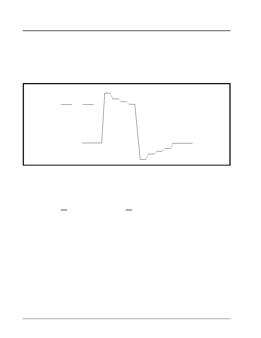
XRT83L30
·Á
·Á
·Á
·Á
ONE-CHANNEL T1/E1/J1 LH/SH TRANSCEIVER WITH CLOCK RECOVERY AND JITTER ATTENUATOR
REV. P1.3.0
PRELIMINARY
23
ARBITRARY PULSE GENERATOR
In T1 mode only, the arbitrary pulse generator divides the pulse into eight individual segments. Each segment
is set by a 7-Bit binary word by programming the appropriate register. This allows the system designer to set
the overshoot, amplitude, and undershoot for a unique line build out. The MSB (bit 7) is a sign-bit. If the sign-bit
is set to "1", the segment will move in a positive direction relative to a flat line (zero) condition. If this sign-bit is
set to "0", the segment will move in a negative direction relative to a flat line condition. A pulse with numbered
segments is shown in Figure 11.
N
OTE
: By default, the arbitrary segments are programmed to 0x00h. The transmitter output will result in an all zero pattern
to the line.
TRANSMITTER
DIGITAL DATA FORMAT
Both the transmitter and receiver can be configured to operate in dual or single-rail data formats. This feature is
available under both Hardware and Host control modes. The dual or single-rail data format is determined by
the state of the SR/DR pin in Hardware mode or SR/DR interface bit in the Host mode. In single-rail mode,
transmit clock and NRZ data are applied to TCLK and TPOS/TDATA pins respectively. In single-rail and
Hardware mode the TNEG/CODE input can be used as the CODES function. With TNEG/CODE tied "Low",
HDB3 or B8ZS encoding and decoding are enabled for E1 and T1 modes respectively. With TNEG/CODE tied
"High", the AMI coding scheme is selected. In both dual or single-rail modes of operations, the transmitter
converts digital input data to a bipolar format before being transmitted to the line.
TRANSMIT CLOCK (TCLK) SAMPLING EDGE
Serial transmit data at TPOS/TDATA and TNEG/CODE are clocked into the XRT83L30 under the
synchronization of TCLK. With a "0" written to the TCLKE interface bit, or by pulling the TCLKE pin "Low", input
data is sampled on the falling edge of TCLK. The sampling edge is inverted with a "1" written to TCLKE
interface bit, or by connecting the TCLKE pin "High".
F
IGURE
11. A
RBITRARY
P
ULSE
S
EGMENT
A
SSIGNMENT
1
2
3
4
5
6
7
8
Segment
Register
1
0xn8
2
0xn9
3
0xna
4
0xnb
5
0xnc
6
0xnd
7
0xne
8
0xnf
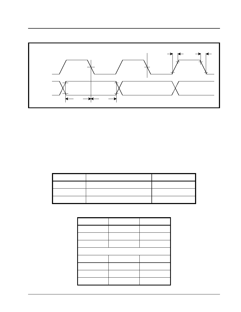
·Á
·Á
·Á
·Á
XRT83L30
ONE-CHANNEL T1/E1/J1 LH/SH TRANSCEIVER WITH CLOCK RECOVERY AND JITTER ATTENUATOR
PRELIMINARY
REV. P1.3.0
24
TRANSMIT HDB3/B8ZS ENCODER
The Encoder function is available in both Hardware and Host modes basis by controlling the TNEG/CODE pin
or CODES interface bit. The encoder is only available in single-rail mode. In E1 mode and with HDB3 encoding
selected, any sequence with four or more consecutive zeros in the input serial data from TPOS/TDATA, will be
removed and replaced with 000V or B00V, where "B" indicates a pulse conforming with the bipolar rule and "V"
representing a pulse violating the rule. An example of HDB3 Encoding is shown in
Table 3
. In a T1 system, an
input data sequence with eight or more consecutive zeros will be removed and replaced using the B8ZS
encoding rule. An example of Bipolar with 8 Zero Substitution (B8ZS) encoding scheme is shown in
Table 4
.
Writing a "
1
" into the CODES interface bit or connecting the TNEG/CODE pin to a "High" level selects the AMI
coding for both E1 or T1 systems.
F
IGURE
12. T
RANSMIT
C
LOCK
AND
I
NPUT
D
ATA
T
IMING
T
ABLE
3: E
XAMPLES
OF
HDB3 E
NCODING
N
UMBER
OF
PULSE
BEFORE
NEXT
4
ZEROS
N
EXT
4
BITS
Input
0000
HDB3 (case1)
odd
000V
HDB3 (case2)
even
B00V
T
ABLE
4: E
XAMPLES
OF
B8ZS E
NCODING
C
ASE
1
P
RECEDING
P
ULSE
N
EXT
8 B
ITS
Input
+
00000000
B8ZS
000VB0VB
AMI Output
+
000+ -0- +
C
ASE
2
Input
-
00000000
B8ZS
000VB0VB
AMI Output
-
000- +0+ -
TCLK
R
TCLK
F
TCLK
TPOS/TDATA
or
TNEG
T
SU
T
HO

XRT83L30
·Á
·Á
·Á
·Á
ONE-CHANNEL T1/E1/J1 LH/SH TRANSCEIVER WITH CLOCK RECOVERY AND JITTER ATTENUATOR
REV. P1.3.0
PRELIMINARY
25
DRIVER FAILURE MONITOR (DMO)
The driver monitor circuit is used to detect transmit driver failure by monitoring the activities at TTIP and
TRING. Driver failure may be caused by a short circuit in the primary transformer or system problems at the
transmit input. If the transmitter has no output for more than 128 clock cycles, the corresponding DMO pin goes
"High" and remains "High" until a valid transmit pulse is detected. In Host mode, the failure of the transmit
channel is reported in the corresponding interface bit. If the DMOIE bit is also enabled, any transition on the
DMO interface bit will generate an interrupt. The driver failure monitor is supported in both Hardware and Host
modes.
TRANSMIT PULSE SHAPER & LINE BUILD OUT (LBO) CIRCUIT
The transmit pulse shaper circuit uses the high speed clock from the Master timing generator to control the
shape and width of the transmitted pulse. The internal high-speed timing generator eliminates the need for a
tightly controlled transmit clock (TCLK) duty cycle. With the jitter attenuator not in the transmit path, the
transmit output will generate no more than 0.025Unit Interval (UI) peak-to-peak jitter. In Hardware mode, the
state of the EQC[4:0] pins determine the transmit pulse shape. In Host mode transmit pulse shape can be
controlled using the interface bits EQC[4:0]. The chip supports five fixed transmit pulse settings for T1 Short-
haul applications plus a fully programmable waveform generator for arbitrary transmit output pulse shapes.
Transmit Line Build-Outs for T1 long-haul application are supported from 0dB to -22.5dB in three 7.5dB steps.
The choice of the transmit pulse shape and LBO under the control of the interface bits are summarized in
Table 5
. For CSU LBO transmit pulse design information, refer to ANSI T1.403-1993 Network-to-Customer
Installation specification, Annex-E.
N
OTE
: EQC[4:0] determine the T1/E1 operating mode of the XRT83L30. When EQC4 = "1" and EQC3 = "1", the XRT83L30
is in the E1 mode, otherwise it is in the T1/J1 mode.
T
ABLE
5: R
ECEIVE
E
QUALIZER
C
ONTROL
AND
T
RANSMIT
L
INE
B
UILD
-O
UT
S
ETTINGS
EQC4 EQC3
EQC2
EQC1
EQC0
E1/T1 M
ODE
& R
ECEIVE
S
ENSITIVITY
T
RANSMIT
LBO
C
ABLE
C
ODING
0
0
0
0
0
T1 Long Haul/36dB
0dB
100
/ TP
B8ZS
0
0
0
0
1
T1 Long Haul/36dB
-7.5dB
100
/ TP
B8ZS
0
0
0
1
0
T1 Long Haul/36dB
-15dB
100
/ TP
B8ZS
0
0
0
1
1
T1 Long Haul/36dB
-22.5dB
100
/ TP
B8ZS
0
0
1
0
0
T1 Long Haul/45dB
0dB
100
/ TP
B8ZS
0
0
1
0
1
T1 Long Haul/45dB
-7.5dB
100
/ TP
B8ZS
0
0
1
1
0
T1 Long Haul/45dB
-15dB
100
/ TP
B8ZS
0
0
1
1
1
T1 Long Haul/45dB
-22.5dB
100
/ TP
B8ZS
0
1
0
0
0
T1 Short Haul/15dB
0-133 ft./ 0.6dB
100
/ TP
B8ZS
0
1
0
0
1
T1 Short Haul/15dB
133-266 ft./ 1.2dB
100
/ TP
B8ZS
0
1
0
1
0
T1 Short Haul/15dB
266-399 ft./ 1.8dB
100
/ TP
B8ZS
0
1
0
1
1
T1 Short Haul/15dB
399-533 ft./ 2.4dB
100
/ TP
B8ZS
0
1
1
0
0
T1 Short Haul/15dB
533-655 ft./ 3.0dB
100
/ TP
B8ZS
0
1
1
0
1
T1 Short Haul/15dB
Arbitrary Pulse
100
/ TP
B8ZS

·Á
·Á
·Á
·Á
XRT83L30
ONE-CHANNEL T1/E1/J1 LH/SH TRANSCEIVER WITH CLOCK RECOVERY AND JITTER ATTENUATOR
PRELIMINARY
REV. P1.3.0
26
0
1
1
1
0
T1 Gain Mode/29dB
0-133 ft./ 0.6dB
100
/ TP
B8ZS
0
1
1
1
1
T1 Gain Mode/29dB
133-266 ft./ 1.2dB
100
/ TP
B8ZS
1
0
0
0
0
T1 Gain Mode/29dB
266-399 ft./ 1.8dB
100
/ TP
B8ZS
1
0
0
0
1
T1 Gain Mode/29dB
399-533 ft./ 2.4dB
100
/ TP
B8ZS
1
0
0
1
0
T1 Gain Mode/29dB
533-655 ft./ 3.0dB
100
/ TP
B8ZS
1
0
0
1
1
T1 Gain Mode/29dB
Arbitrary Pulse
100
/ TP
B8ZS
1
0
1
0
0
T1 Gain Mode/29dB
0dB
100
/ TP
B8ZS
1
0
1
0
1
T1 Gain Mode/29dB
-7.5dB
100
/ TP
B8ZS
1
0
1
1
0
T1 Gain Mode/29dB
-15dB
100
/ TP
B8ZS
1
0
1
1
1
T1 Gain Mode/29dB
-22.5dB
100
/ TP
B8ZS
1
1
0
0
0
E1 Long Haul/36dB
ITU G.703
75
Coax
HDB3
1
1
0
0
1
E1 Long Haul/36dB
ITU G.703
120
TP
HDB3
1
1
0
1
0
E1 Long Haul/43dB
ITU G.703
75
Coax
HDB3
1
1
0
1
1
E1 Long Haul/43dB
ITU G.703
120
TP
HDB3
1
1
1
0
0
E1 Short Haul
ITU G.703
75
Coax
HDB3
1
1
1
0
1
E1 Short Haul
ITU G.703
120
TP
HDB3
1
1
1
1
0
E1 Gain Mode
ITU G.703
75
Coax
HDB3
1
1
1
1
1
E1 Gain Mode
ITU G.703
120
TP
HDB3
T
ABLE
5: R
ECEIVE
E
QUALIZER
C
ONTROL
AND
T
RANSMIT
L
INE
B
UILD
-O
UT
S
ETTINGS
EQC4 EQC3
EQC2
EQC1
EQC0
E1/T1 M
ODE
& R
ECEIVE
S
ENSITIVITY
T
RANSMIT
LBO
C
ABLE
C
ODING
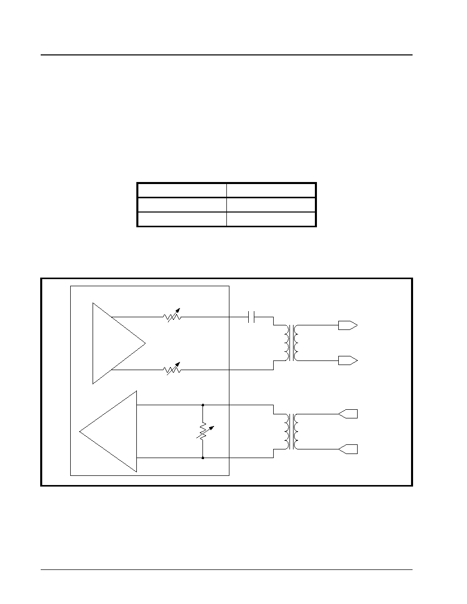
XRT83L30
·Á
·Á
·Á
·Á
ONE-CHANNEL T1/E1/J1 LH/SH TRANSCEIVER WITH CLOCK RECOVERY AND JITTER ATTENUATOR
REV. P1.3.0
PRELIMINARY
27
TRANSMIT AND RECEIVE TERMINATIONS
The XRT83L30 is a versatile LIU that can be programmed to use one Bill of Materials (BOM) for worldwide
applications for T1, J1 and E1. For specific applications the internal terminations can be disabled to allow the
use of existing components and/or designs.
RECEIVER
I
NTERNAL
R
ECEIVE
T
ERMINATION
M
ODE
In Hardware mode, RXTSEL (Pin 44) can be tied "High" to select internal termination mode or tied "Low" to
select external termination mode. By default the XRT83L30 is set for external termination mode at power up or
at Hardware reset.
In Host mode, bit 7 in the appropriate register, (
Table 20, "Microprocessor Register #1, Bit Description," on
page 47
), is set "High" to select the internal termination mode for the receive channel.
If the internal termination mode (RXTSEL = "1") is selected, the effective impedance for E1, T1 or J1 can be
achieved either with an internal resistor or a combination of internal and external resistors as shown in
Table 7
.
T
ABLE
6: R
ECEIVE
T
ERMINATION
C
ONTROL
RXTSEL
RX TERMINATION
0
EXTERNAL
1
INTERNAL
F
IGURE
13. S
IMPLIFIED
D
IAGRAM
FOR
THE
I
NTERNAL
R
ECEIVE
AND
T
RANSMIT
T
ERMINATION
M
ODE
T1
TTIP
TRING
5
8
1:2
75
, 100
110
or 120
4
1
0.68
µ
F
R
int
R
int
TTIP
TRING
TX
Line Driver
T2
RTIP
RRING
1
4
1:1
8
5
RTIP
RRING
RX
Equalizer
R
int
TPOS
TNEG
TCLK
RPOS
RNEG
RCLK
75
, 100
110
or 120
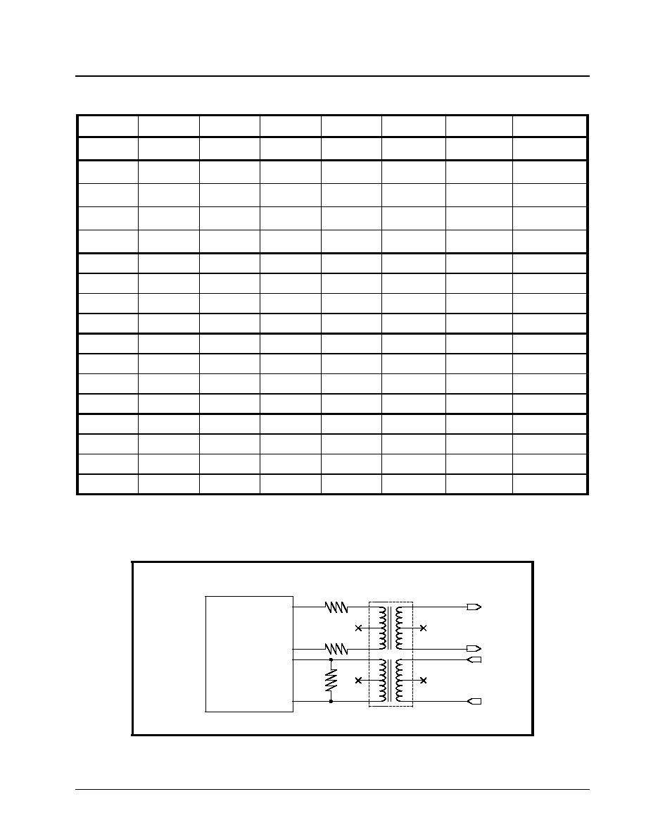
·Á
·Á
·Á
·Á
XRT83L30
ONE-CHANNEL T1/E1/J1 LH/SH TRANSCEIVER WITH CLOCK RECOVERY AND JITTER ATTENUATOR
PRELIMINARY
REV. P1.3.0
28
Figure 14
is a simplified diagram for T1 (100
) in the external receive termination mode.
Figure 15
is a
simplified diagram for E1 (75
) in the external receive termination mode.
T
ABLE
7: R
ECEIVE
T
ERMINATIONS
RXTSEL
TERSEL1
TERSEL0
RXRES1
RXRES0
R
ext
R
int
M
ODE
0
x
x
x
x
R
ext
T1/E1/J1
1
0
0
0
0
100
T1
1
0
1
0
0
110
J1
1
1
0
0
0
75
E1
1
1
1
0
0
120
E1
1
0
0
0
1
240
172
T1
1
0
1
0
1
240
204
J1
1
1
0
0
1
240
108
E1
1
1
1
0
1
240
240
E1
1
0
0
1
0
210
192
T1
1
0
1
1
0
210
232
J1
1
1
0
1
0
210
116
E1
1
1
1
1
0
210
280
E1
1
0
0
1
1
150
300
T1
1
0
1
1
1
150
412
J1
1
1
0
1
1
150
150
E1
1
1
1
1
1
150
600
E1
F
IGURE
14. S
IMPLIFIED
D
IAGRAM
FOR
T1
IN
THE
E
XTERNAL
T
ERMINATION
M
ODE
(RXTSEL= 0)
3.1
3.1
TTIP
TRING
RTIP
RRING
XRT83L30 LIU
100
100
100
1:2 or
1:2.45
1:1
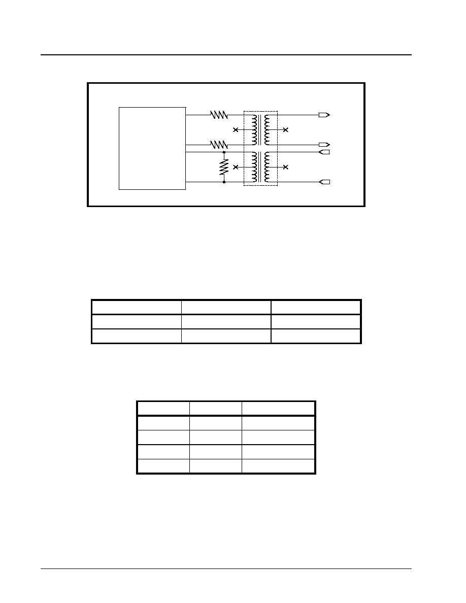
XRT83L30
·Á
·Á
·Á
·Á
ONE-CHANNEL T1/E1/J1 LH/SH TRANSCEIVER WITH CLOCK RECOVERY AND JITTER ATTENUATOR
REV. P1.3.0
PRELIMINARY
29
TRANSMITTER
T
RANSMIT
T
ERMINATION
M
ODE
In Hardware mode, TXTSEL (Pin 45) can be tied "High" to select internal termination mode or tied "Low" for
external termination. In Host mode, bit 6 in the appropriate register is set "High" to select the internal
termination mode for the transmit channel, see
Table 19, "Microprocessor Register #1 bit description," on
page 46
.
For internal termination, the transformer turns ratio is always 1:2. In internal mode, no external resistors are
used. An external capacitor of 0.68
µ
F is used for proper operation of the internal termination circuitry, see
Figure 13
.
E
XTERNAL
T
RANSMIT
T
ERMINATION
M
ODE
By default the XRT83L30 is set for external termination mode at power up or at Hardware reset.
When external transmit termination mode is selected, the internal termination circuitry is disabled. The value of
the external resistors is chosen for a specific application according to the turns ratio selected by TRATIO (Pin
26) in Hardware mode or bit 0 in the appropriate register in Host mode, see
Table 10
and
Table 21,
"Microprocessor Register #3 bit description," on page 50
.
Figure 14
is a simplified block diagram for T1 (100
)
in the external termination mode.
Figure 15
is a simplified block diagram for E1 (75
) in the external
termination mode.
F
IGURE
15. S
IMPLIFIED
D
IAGRAM
FOR
E1
IN
E
XTERNAL
T
ERMINATION
M
ODE
(RXTSEL= 0)
T
ABLE
8: T
RANSMIT
T
ERMINATION
C
ONTROL
TXTSEL
TX TERMINATION
T
X
T
RANSFORMER
R
ATIO
0
EXTERNAL
1:2.45
1
INTERNAL
1:2
T
ABLE
9: T
ERMINATION
S
ELECT
C
ONTROL
TERSEL1
TERSEL0
TERMINATION
0
0
100
0
1
110
1
0
75
1
1
120
9.1
9.1
TTIP
TRING
RTIP
RRING
75
XRT83L30 LIU
75
75
1:2
1:1

·Á
·Á
·Á
·Á
XRT83L30
ONE-CHANNEL T1/E1/J1 LH/SH TRANSCEIVER WITH CLOCK RECOVERY AND JITTER ATTENUATOR
PRELIMINARY
REV. P1.3.0
30
Table 11
summarizes the transmit terminations.
REDUNDANCY APPLICATIONS
Telecommunication system design requires signal integrity and reliability. When a T1/E1 primary line card has
a failure, it must be swapped with a backup line card while maintaining connectivity to a backplane without
losing data. System designers can achieve this by implementing common redundancy schemes with the
XRT83L30 Line Interface Unit (LIU). The XRT83L30 offers features that are tailored to redundancy applications
while reducing the number of components and providing system designers with solid reference designs. These
features allow system designers to implement redundancy applications that ensure reliability. The Internal
Impedance mode eliminates the need for external relays when using the 1:1 and 1+1 redundancy schemes.
T
ABLE
10: T
RANSMIT
T
ERMINATION
C
ONTROL
TRATIO
T
URNS
R
ATIO
0
1:2
1
1:2.45
T
ABLE
11: T
RANSMIT
T
ERMINATIONS
TERSEL1
TERSEL0
TXTSEL
TRATIO
R
int
n
R
ext
C
ext
0=
EXTERNAL
SET
BY
CONTROL
BITS
n, R
ext
,
AND
C
ext
ARE
SUGGESTED
SETTINGS
1=
INTERNAL
T1
100
0
0
0
0
0
2.45
3.1
0
0
0
0
1
0
2
3.1
0
0
0
1
x
25
2
0
0.68
µ
F
J1
110
0
1
0
0
0
2.45
3.1
0
0
1
0
1
0
2
3.1
0
0
1
1
x
27.5
2
0
0.68
µ
F
E1
75
1
0
0
0
0
2.45
6.2
0
1
0
0
1
0
2
9.1
0
1
0
1
x
18.75
2
0
0.68
µ
F
E1
120
1
1
0
0
0
2.45
6.2
0
1
1
0
1
0
2
9.1
0
1
1
1
x
30
2
0
0.68
µ
F

XRT83L30
·Á
·Á
·Á
·Á
ONE-CHANNEL T1/E1/J1 LH/SH TRANSCEIVER WITH CLOCK RECOVERY AND JITTER ATTENUATOR
REV. P1.3.0
PRELIMINARY
31
PROGRAMMING CONSIDERATIONS
In many applications switching the control of the transmitter outputs and the receiver line impedance to
hardware control will provide faster transmitter ON/OFF switching.
In Host Mode, there are two bits in register 18 (12H) that control the transmitter outputs and the Rx line
impedance select, TXONCNTL (Bit 5) and TERCNTL (Bit 4).
Setting bit-5 (TXONCNTL) to a "1" transfers the control of the Transmit On/Off function to the TXON Hardware
control pin (pin 58).
Setting bit-4 (TERCNTL) to a "1" transfers the control of the Rx line impedance select (RXTSEL) to the
RXTSEL Hardware control pin (pin 44).
Either mode works well with redundancy applications. The user can determine which mode has the fastest
switching time for a unique application.
TYPICAL REDUNDANCY SCHEMES
s
∑1:1 One backup card for every primary card (Facility Protection)
s
∑1+1 One backup card for every primary card (Line Protection)
s
∑N+1One backup card for N primary cards
1:1 REDUNDANCY
A 1:1 facility protection redundancy scheme has one backup card for every primary card. When using 1:1
redundancy, the backup card has its transmitters tri-stated and its receivers in high impedance. This eliminates
the need for external relays and provides one bill of materials for all interface modes of operation. The transmit
and receive sections of the LIU device are described separately.
1+1 REDUNDANCY
A 1+1 line protection redundancy scheme has one backup card for every primary card, and the receivers on
the backup card are monitoring the receiver inputs. Therefore, the receivers on both cards need to be active.
The transmit outputs require no external resistors. The transmit and receive sections of the LIU device are
described separately.
TRANSMIT 1:1 & 1+1 REDUNDANCY
For 1:1 and 1+1 redundancy, the transmitters on the primary and backup card should be programmed for
Internal Impedance mode. The transmitters on the backup card should be tri-stated. Select the appropriate
impedance for the desired mode of operation, T1/E1/J1. A 0.68uF capacitor is used in series with TTIP for
blocking DC bias. See
Figure 16
for a simplified block diagram of the transmit section for 1:1 and 1+1
redundancy scheme.
N
OTE
: For simplification, the over voltage protection circuitry was omitted.
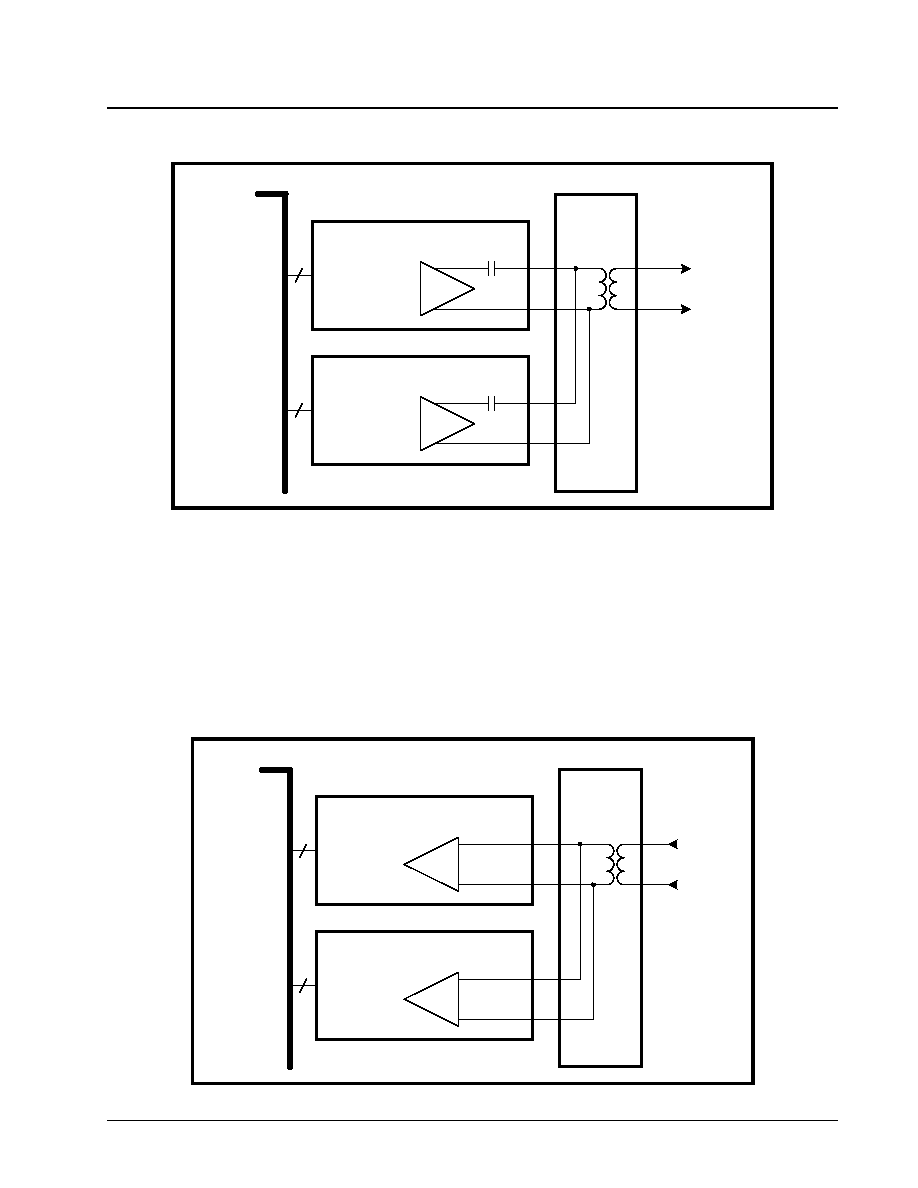
·Á
·Á
·Á
·Á
XRT83L30
ONE-CHANNEL T1/E1/J1 LH/SH TRANSCEIVER WITH CLOCK RECOVERY AND JITTER ATTENUATOR
PRELIMINARY
REV. P1.3.0
32
RECEIVE 1:1 & 1+1 REDUNDANCY
For 1:1 and 1+1 redundancy, the receivers on the primary card should be programmed for Internal Impedance
mode. The receivers on the backup card should be programmed for External Impedance mode. Since there is
no external resistor in the circuit, the receivers on the backup card will be high impedance. This key design
feature eliminates the need for relays and provides one bill of materials for all interface modes of operation.
Select the impedance for the desired mode of operation, T1/E1/J1. To swap the primary card, set the backup
card to Internal Impedance mode, then the primary card to External Impedance mode. See
Figure 17
for a
simplified block diagram of the receive section for a 1:1 and 1+1 redundancy scheme.
N
OTE
: For simplification, the over voltage protection circuitry was omitted.
F
IGURE
16. S
IMPLIFIED
B
LOCK
D
IAGRAM
OF
THE
T
RANSMIT
S
ECTION
FOR
1:1 & 1+1 R
EDUNDANCY
F
IGURE
17. S
IMPLIFIED
B
LOCK
D
IAGRAM
- R
ECEIVE
S
ECTION
FOR
1:1
AND
1+1 R
EDUNDANCY
T1/E1 Line
Backplane Interface
Primary Card
Backup Card
XRT83L30
XRT83L30
Tx
Tx
Line Interface Card
0.68
µ
F
0.68
µ
F
TxTSEL=1, Internal
TxTSEL=1, Internal
1:2
RxTSEL=0, External
RxTSEL=1, Internal
Backplane Interface
Primary Card
Backup Card
XRT83L30
XRT83L30
Rx
Line Interface Card
T1/E1 Line
Rx
1:1
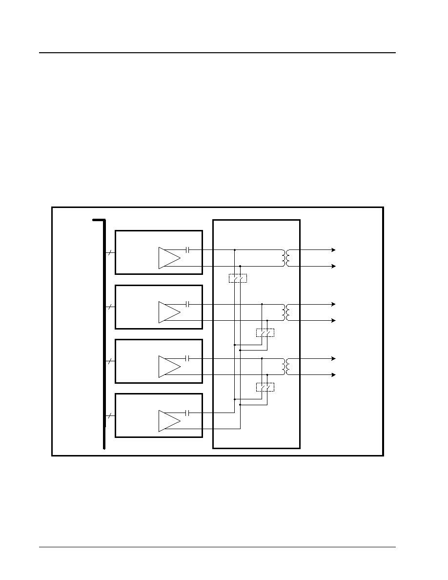
XRT83L30
·Á
·Á
·Á
·Á
ONE-CHANNEL T1/E1/J1 LH/SH TRANSCEIVER WITH CLOCK RECOVERY AND JITTER ATTENUATOR
REV. P1.3.0
PRELIMINARY
33
N+1 REDUNDANCY
N+1 redundancy has one backup card for N primary cards. Due to impedance mismatch and signal contention,
external relays are necessary when using this redundancy scheme. The advantage of relays is that they create
complete isolation between the primary cards and the backup card. This allows all transmitters and receivers
on the primary cards to be configured in internal impedance mode, providing one bill of materials for all
interface modes of operation. The transmit and receive sections of the XRT83L30 are described separately.
TRANSMIT
For N+1 redundancy, the transmitters on all cards should be programmed for internal impedance mode
providing one bill of materials for T1/E1/J1. The transmitters on the backup card do not have to be tri-stated. To
swap the primary card, close the desired relays, and tri-state the transmitters on the failed primary card. A
0.68
µ
F capacitor is used in series with TTIP for blocking DC bias. See
Figure 18
for a simplified block diagram
of the transmit section for an N+1 redundancy scheme.
N
OTE
: For simplification, the over voltage protection circuitry was omitted.
F
IGURE
18. S
IMPLIFIED
B
LOCK
D
IAGRAM
- T
RANSMIT
S
ECTION
FOR
N+1 R
EDUNDANCY
Backplane Interface
Primary Card
XRT83L30
Tx
Line Interface Card
0.68
µ
F
T1/E1 Line
Primary Card
XRT83L30
Tx
Primary Card
XRT83L30
Tx
Backup Card
XRT83L30
Tx
T1/E1 Line
T1/E1 Line
TxTSEL=1, Internal
TxTSEL=1, Internal
TxTSEL=1, Internal
TxTSEL=1, Internal
1:2
0.68
µ
F
0.68
µ
F
0.68
µ
F
1:2
1:2
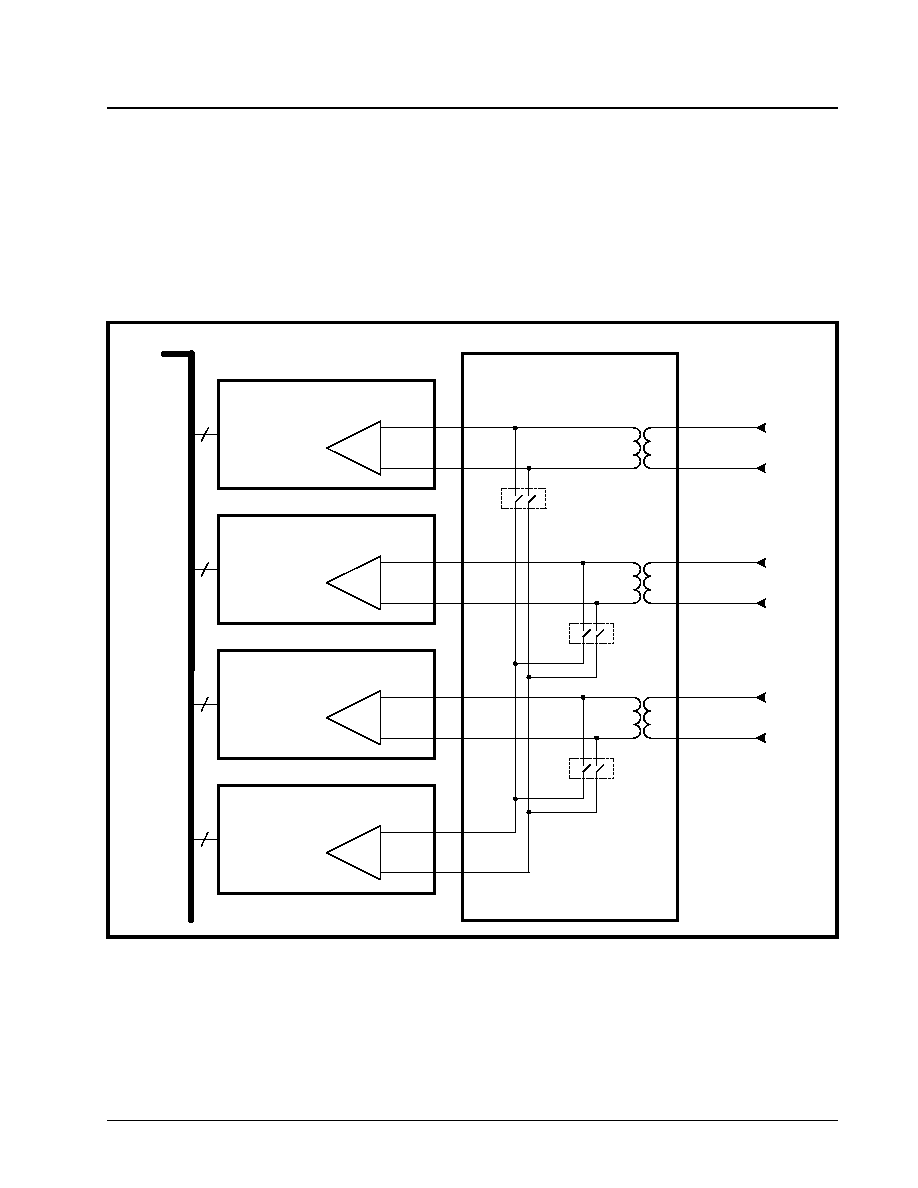
·Á
·Á
·Á
·Á
XRT83L30
ONE-CHANNEL T1/E1/J1 LH/SH TRANSCEIVER WITH CLOCK RECOVERY AND JITTER ATTENUATOR
PRELIMINARY
REV. P1.3.0
34
RECEIVE
For N+1 redundancy, the receivers on the primary cards should be programmed for internal impedance mode.
The receivers on the backup card should be programmed for external impedance mode. Since there is no
external resistor in the circuit, the receivers on the backup card will be high impedance. Select the impedance
for the desired mode of operation, T1/E1/J1. To swap the primary card, set the backup card to internal
impedance mode, then the primary card to external impedance mode. See
Figure 19
. for a simplified block
diagram of the receive section for a N+1 redundancy scheme.
N
OTE
: For simplification, the over voltage protection circuitry was omitted.
F
IGURE
19. S
IMPLIFIED
B
LOCK
D
IAGRAM
- R
ECEIVE
S
ECTION
FOR
N+1 R
EDUNDANCY
Backplane Interface
Primary Card
XRT83L30
Rx
Line Interface Card
Primary Card
XRT83L30
Rx
Primary Card
XRT83L30
Rx
Backup Card
XRT83L30
Rx
RxTSEL=1, Internal
RxTSEL=1, Internal
RxTSEL=1, Internal
RxTSEL=1, External
T1/E1 Line
T1/E1 Line
T1/E1 Line
1:1
1:1
1:1

XRT83L30
·Á
·Á
·Á
·Á
ONE-CHANNEL T1/E1/J1 LH/SH TRANSCEIVER WITH CLOCK RECOVERY AND JITTER ATTENUATOR
REV. P1.3.0
PRELIMINARY
35
PATTERN TRANSMIT AND DETECT FUNCTION
Several test and diagnostic patterns can be generated and detected by the chip. In Hardware mode the
channel can be programmed to transmit an All Ones pattern by applying a "High" level to the corresponding
TAOS pin. In Host mode, the three interface bits TXTEST[2:0] control the pattern generation and detection
according to
Table 12
.
TRANSMIT ALL ONES (TAOS)
This feature is available in both Hardware and Host modes. When the Hardware pins or interface bits
TXTEST2="0", TXTEST1="0" and TXTEST0="1", the transmitter ignores input from TPOS/TDATA and TNEG
pins and sends a continuous AMI encoded all ones signal to the line using TCLK clock as the reference. When
TCLK is not available, MCLK is used. In addition, when the Hardware pin or the interface bit ATAOS is
activated, the chip will automatically transmit the All Ones data when the receiver detects an RLOS condition.
The operation of this feature requires that TCLK not be tied "Low".
NETWORK LOOP CODE DETECTION AND TRANSMISSION
This feature is available in both Hardware and Host modes. When the Hardware pins or interface bits
TXTEST2="0", TXTEST1="1" and TXTEST0="0" the chip is enabled to transmit the "00001" Network Loop-Up
Code from a request for a loop-back condition from the remote terminal. Simultaneously setting the interface
bits NLCDE1="0" and NLCDE0="1" enables the Network Loop-Up code detection in the receiver. If the "00001"
Network Loop-Up code is detected in the receive data for longer than 5 seconds, the NLCD bit in the interface
register is set indicating that the remote terminal has activated remote Loop-back and the chip is receiving its
own transmitted data. When Network Loop-Up code is being transmitted the XRT83L30 will ignore the Auto-
matic Loop-Code detection and Remote Loop-back activation (NLCDE1="1", NLCDE0="1", if activated) in
order to avoid activating Remote Digital Loop-back automatically when the remote terminal responds to the
Loop-back request.
When TXTEST2="0", TXTEST1="1" and TXTEST0="1" the chip is enabled to transmit the Network Loop-Down
Code "001" from the transmitter requesting the remote terminal the removal of the Loop-Back condition.
In both Hardware and Host modes the receiver is capable of monitoring the contents of the receive data for
the presence of Loop-Up or Loop-Down code from the remote terminal. The Hardware pins or interface bits
T
ABLE
12: P
ATTERN
TRANSMISSION
CONTROL
TXTEST2
TXTEST1
TXTEST0
T
EST
P
ATTERN
0
0
0
Transmit Data
0
0
1
TAOS
0
1
0
TLUC
0
1
1
TLDC
1
0
0
TDQRSS
1
0
1
TDQRSS & INVQRSS
1
1
0
TDQRSS & INSBER
1
1
1
TDQRSS & INVQRSS & INSBER

·Á
·Á
·Á
·Á
XRT83L30
ONE-CHANNEL T1/E1/J1 LH/SH TRANSCEIVER WITH CLOCK RECOVERY AND JITTER ATTENUATOR
PRELIMINARY
REV. P1.3.0
36
NLCDE[1:0] control the Loop-Code detection according to Table 13
.
Setting the Hardware pins or interface bits NLCDE1="0" and NLCDE0="1" activates the detection of the Loop-
Up code in the receive data. If the "00001" Network Loop-Up code is detected in the receive data for longer
than 5 seconds the NLCD interface bit is set to "1" and stays in this state for as long as the receiver continues
to receive the Network Loop-Up Code. In this mode if the NLCD interrupt is enabled, the chip will initiate an
interrupt on every transition of NLCD. The host has the option to ignore the request from the remote terminal,
or to respond to the request and manually activate Remote Loop-Back. The host can subsequently activate the
detection of the Loop-Down Code by setting NLCDE1="1" and NLCDE0="0". In this case, receiving the "001"
Loop-Down Code for longer than 5 seconds will set the NLCD bit to "1" and if the NLCD interrupt is enabled,
the chip will initiate an interrupt on every transition of NLCD. The host can respond to the request from the
remote terminal and remove Loop-Back condition. In the manual Network Loop-Up (NLCDE1="0" and
NLCDE0="1") and Loop-Down (NLCDE1="1" and NLCDE0="0") Code detection modes, the NLCD pin or
interface bit will be set to "1" upon receiving the corresponding code in excess of 5 seconds in the receive data.
In Host mode the chip will initiate an interrupt any time the status of the NLCD bit changes and the Network
Loop-code interrupt is enabled.
Setting the Hardware pins or interface bits NLCDE1="1" and NLCDE0="1" enables the automatic Loop-Code
detection and Remote Loop-Back activation mode if, TXTEST[2:0] is NOT equal to "110". As this mode is
initiated, the state of the NLCD pin or interface bit is reset to "0" and the chip is programmed to monitor the
receive input data for the Loop-Up Code. If the "00001" Network Loop-Up Code is detected in the receive data
for longer than 5 seconds in addition to setting the NLCD pin or interface bit, Remote loop-back is automatically
activated. The chip stays in remote loop-back even if it stops receiving the "00001" pattern. After the chip
detects the Loop-Up code, sets the NLCD pin (bit) and enters Remote loop-back, it automatically starts
monitoring the receive data for the Loop-Down code. In this mode however, the NLCD pin (bit) stays set even if
the receiver stops receiving the Loop-Up code, which is an indication to the host that the Remote loop-back is
still in effect. Remote loop-back is removed if the chip detects the "001" Loop-Down code for longer than 5
seconds. Detecting the "001" code also results in resetting the NLCD pin (bit) and initiating an interrupt. The
Remote loop-back can also be removed by taking the chip out of the Automatic detection mode by
programming it to operate in a different state. The chip will not respond to remote loop-back request if an
Analog loop-back is activated locally. When programmed in Automatic detection mode the NLCD pin (bit) stays
"High" for the whole time the Remote loop-back is activated and in the Host mode it initiates an interrupt any
time the status of the NLCD bit changes provided the Network Loop-code interrupt is enabled.
TRANSMIT AND DETECT QUASI-RANDOM SIGNAL SOURCE (TDQRSS)
The XRT83L30 includes a QRSS pattern generation and detection block for diagnostic purposes that can be
activated only in the Host mode by setting the interface bits TXTEST2="1", TXTEST1="0" and TXTEST0="0".
For T1 systems, the QRSS pattern is a 2
20
-1pseudo-random bit sequence (PRBS) with no more than 14
consecutive zeros. For E1 systems, the QRSS pattern is 2
15
-1 PRBS with an inverted output. With QRSS and
Analog Local Loop-Back enabled simultaneously, and by monitoring the status of the QRPD interface bit, all
main functional blocks within the transceiver can be verified.
When the receiver achieves QRSS synchronization with fewer than 4 errors in a 128 bits window, QRPD
changes from "Low" to "High". After pattern synchronization, any bit error will cause QRPD to go "Low" for one
clock cycle. If the QRPDIE bit is enabled, any transition on the QRPD bit will generate an interrupt.
T
ABLE
13: L
OOP
-C
ODE
D
ETECTION
C
ONTROL
NLCDE1
NLCDE0
CONDITION
0
0
Disable Loop-Code Detection
0
1
Detect Loop-Up Code in Receive Data
1
0
Detect Loop-Down Code in Receive Data
1
1
Automatic Loop-Code detection and Remote Loop-Back Activation

XRT83L30
·Á
·Á
·Á
·Á
ONE-CHANNEL T1/E1/J1 LH/SH TRANSCEIVER WITH CLOCK RECOVERY AND JITTER ATTENUATOR
REV. P1.3.0
PRELIMINARY
37
With TDQRSS activated, a bit error can be inserted in the transmitted QRSS pattern by transitioning the
INSBER interface bit from "0" to "1". Bipolar violation can also be inserted either in the QRSS pattern, or input
data when operating in the single-rail mode by transitioning the INSBPV interface bit from "0" to "1". The state
of INSBER and INSBPV bits are sampled on the rising edge of the TCLK. To insure the insertion of the bit error
or bipolar violation, a "0" should be written in these bit locations before writing a "1".
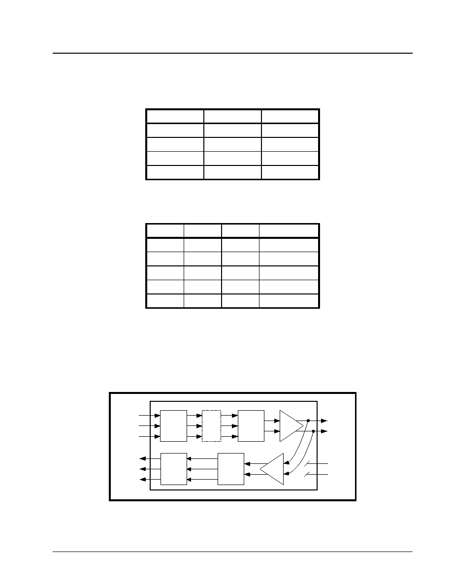
·Á
·Á
·Á
·Á
XRT83L30
ONE-CHANNEL T1/E1/J1 LH/SH TRANSCEIVER WITH CLOCK RECOVERY AND JITTER ATTENUATOR
PRELIMINARY
REV. P1.3.0
38
LOOP-BACK MODES
The XRT83L30 supports several Loop-Back modes under both Hardware and Host control. In Hardware
mode the two LOOP[1:0] pins control the Loop-Back functions according to
Table 14
.
In Host mode the Loop-Back functions are controlled by the three LOOP[2:0] interface bits. The LIU can be
programmed according to
Table 15
.
LOCAL ANALOG LOOP-BACK (ALOOP)
With Local Analog Loop-Back activated, the transmit data at TTIP and TRING are looped-back to the analog
input of the receiver. External inputs at RTIP/RRING in this mode are ignored while valid transmit data
continues to be sent to the line. Local Analog Loop-Back exercises most of the functional blocks of the
XRT83L30 including the jitter attenuator which can be selected in either the transmit or receive paths. Local
Analog Loop-Back is shown in
Figure 20
.
In this mode, the jitter attenuator (if selected) can be placed in the transmit or receive path.
T
ABLE
14: L
OOP
-
BACK
CONTROL
IN
H
ARDWARE
MODE
LOOP1
LOOP0
L
OOP
-
BACK
M
ODE
0
0
None
0
1
Analog
1
0
Remote
1
1
Digital
T
ABLE
15: L
OOP
-
BACK
CONTROL
IN
H
OST
MODE
LOOP2
LOOP1
LOOP0
L
OOP
-
BACK
M
ODE
0
X
X
None
1
0
0
Dual
1
0
1
Analog
1
1
0
Remote
1
1
1
Digital
F
IGURE
20. L
OCAL
A
NALOG
L
OOP
-
BACK
SIGNAL
FLOW
Rx
Data &
Clock
Recovery
Decoder
TPOS
TNEG
TCLK
RCLK
RPOS
RNEG
Tx
Encoder
Timing
Control
JA
TTIP
TRING
RTIP
RRING
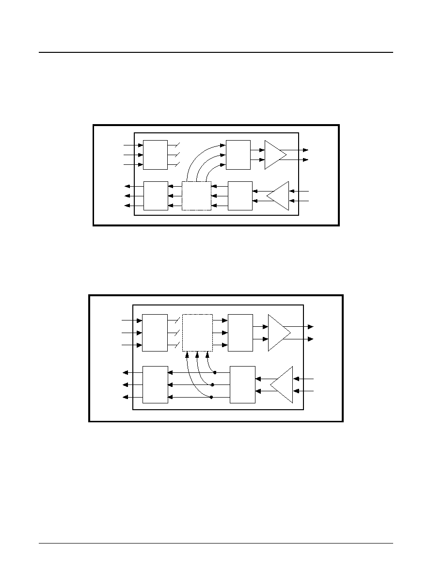
XRT83L30
·Á
·Á
·Á
·Á
ONE-CHANNEL T1/E1/J1 LH/SH TRANSCEIVER WITH CLOCK RECOVERY AND JITTER ATTENUATOR
REV. P1.3.0
PRELIMINARY
39
REMOTE LOOP-BACK (RLOOP)
With Remote Loop-Back activated, receive data after the jitter attenuator (if selected in the receive path) is
looped back to the transmit path using RCLK as transmit timing. In this mode transmit clock and data are
ignored, while RCLK and receive data will continue to be available at their respective output pins. Remote
Loop-Back with jitter attenuator selected in the receive path is shown in
Figure 21
.
In the Remote Loop-Back mode if the jitter attenuator is selected in the transmit path, the receive data from the
Clock and Data Recovery block is looped back to the transmit path and is applied to the jitter attenuator using
RCLK as transmit timing. In this mode the transmit clock and data are also ignored, while RCLK and received
data will continue to be available at their respective output pins. Remote Loop-Back with the jitter attenuator
selected in the transmit path is shown in
Figure 22
.
F
IGURE
21. R
EMOTE
L
OOP
-
BACK
MODE
WITH
JITTER
ATTENUATOR
SELECTED
IN
RECEIVE
PATH
F
IGURE
22. R
EMOTE
L
OOP
-
BACK
MODE
WITH
JITTER
ATTENUATOR
SELECTED
IN
T
RANSMIT
PATH
Tx
Decoder
Timing
Control
Rx
Data &
Clock
Recovery
TPOS
TNEG
TCLK
RCLK
RPOS
RNEG
Encoder
TTIP
TRING
RTIP
RRING
JA
Tx
Decoder
Timing
Control
Rx
Clock &
Data
Recovery
JA
TPOS
TNEG
TCLK
RCLK
RPOS
RNEG
Encoder
TTIP
TRING
RTIP
RRING
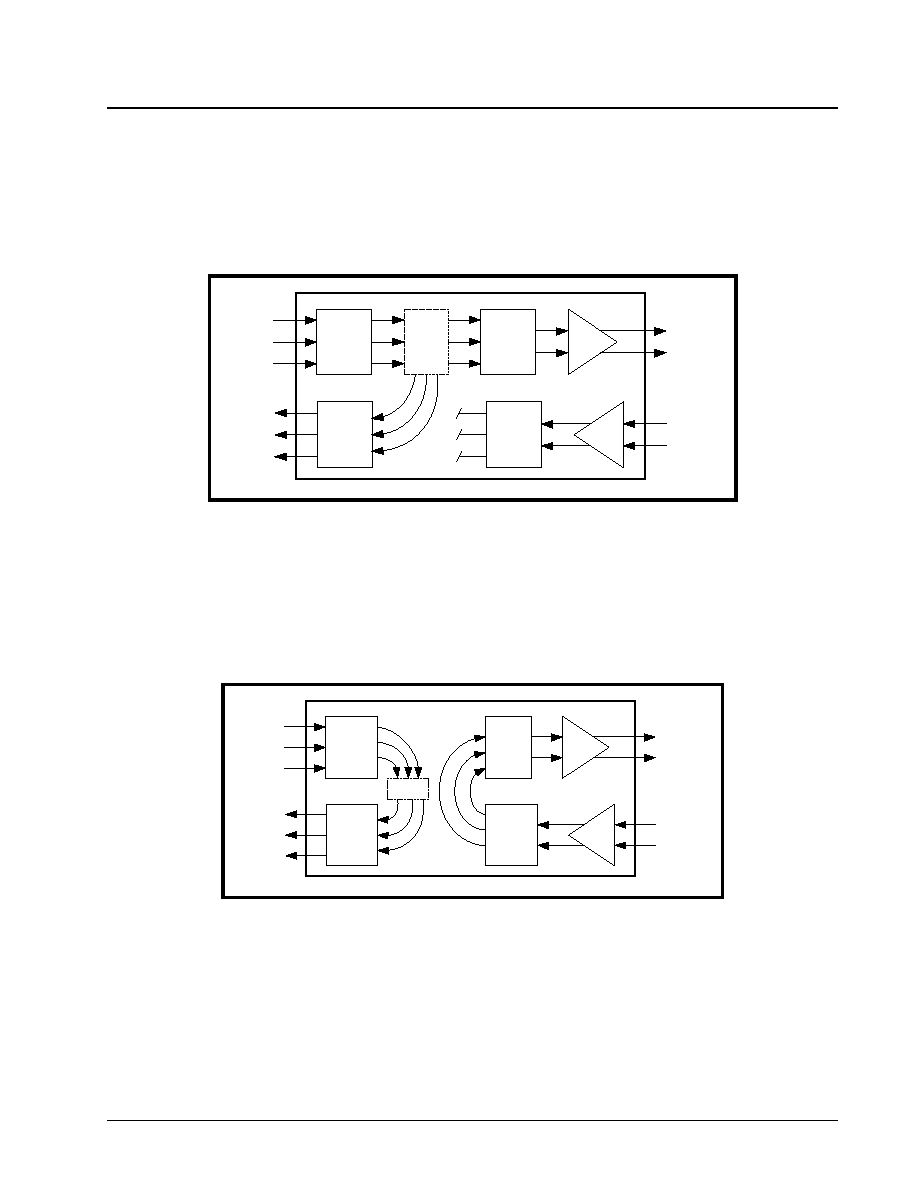
·Á
·Á
·Á
·Á
XRT83L30
ONE-CHANNEL T1/E1/J1 LH/SH TRANSCEIVER WITH CLOCK RECOVERY AND JITTER ATTENUATOR
PRELIMINARY
REV. P1.3.0
40
DIGITAL LOOP-BACK (DLOOP)
Digital Loop-Back or Local Loop-Back allows the transmit clock and data to be looped back to the
corresponding receiver output pins through the encoder/decoder and jitter attenuator. In this mode, receive
data and clock are ignored, but the transmit data will be sent to the line uninterrupted. This loop back feature
allows users to configure the line interface as a pure jitter attenuator. The Digital Loop-Back signal flow is
shown in
Figure 23
.
DUAL LOOP-BACK
Figure 24
depicts the data flow in dual-loopback. In this mode, selecting the jitter attenuator in the transmit path
will have the same result as placing the jitter attenuator in the receive path. In dual Loop-Back mode the
recovered clock and data from the line are looped back through the transmitter to the TTIP and TRING without
passing through the jitter attenuator. The transmit clock and data are looped back through the jitter attenuator
to the RCLK and RPOS/RDATA and RNEG pins.
F
IGURE
23. D
IGITAL
L
OOP
-
BACK
MODE
WITH
JITTER
ATTENUATOR
SELECTED
IN
T
RANSMIT
PATH
F
IGURE
24. S
IGNAL
FLOW
IN
D
UAL
LOOP
-
BACK
MODE
Tx
Decoder
Timing
Control
Rx
Data &
Clock
Recovery
JA
TPOS
TNEG
TCLK
RCLK
RPOS
RNEG
Encoder
TTIP
TRING
RTIP
RRING
Tx
Decoder
Timing
Control
Rx
Data &
Clock
Recovery
JA
TPOS
TNEG
TCLK
RCLK
RPOS
RNEG
Encoder
TTIP
TRING
RTIP
RRING

XRT83L30
·Á
·Á
·Á
·Á
ONE-CHANNEL T1/E1/J1 LH/SH TRANSCEIVER WITH CLOCK RECOVERY AND JITTER ATTENUATOR
REV. P1.3.0
PRELIMINARY
41
HOST MODE SERIAL INTERFACE OPERATION
XRT83L30 has a simple four wire Serial Interface that is compatible with many of the microcontrollers available
in the market. The Host mode operation is enabled by connecting pin 20 (HW/HOST) to a "Low". The Serial
Interface provides a total of 32 "Read/Write" 8-bit registers that consists of the following signals:
CS
-
Chip Select (Active "Low")
SCLK
-
Serial Clock
SDI
-
Serial Data Input
SDO
-
Serial Data Output
USING THE MICROPROCESSOR SERIAL INTERFACE
The following instructions for using the Microprocessor Serial Interface are best understood by referring to the
diagram in Figure 25.
In order to use the Serial interface, a clock signal must be applied to the SCLK input pin. The maximum SCLK
clock frequency is 20MHz. A Read or Write operation can then be initiated by asserting the active-low Chip
Select (CS) input pin. For proper operation the CS must be asserted "Low" at least 50ns prior to the first rising
edge of the SCLK. Once the CS pin has been asserted, the Read/Write Operation and the target register can
be specified through the Serial Interface by writing eight serial bits into the SDI input. Each bit will be clocked
on the rising edge of SCLK.The function of the eight bits are identified and described below:
Bit 1:
R/W (Read/Write) Bit
This bit is clocked into the SDI input on the first rising edge of the SCLK after CS has been asserted. This bit
indicates whether the current operation is a "Read" or a "Write". A "1" in this bit specifies a Read operation,
whereas a "0" specifies a "Write" operation.
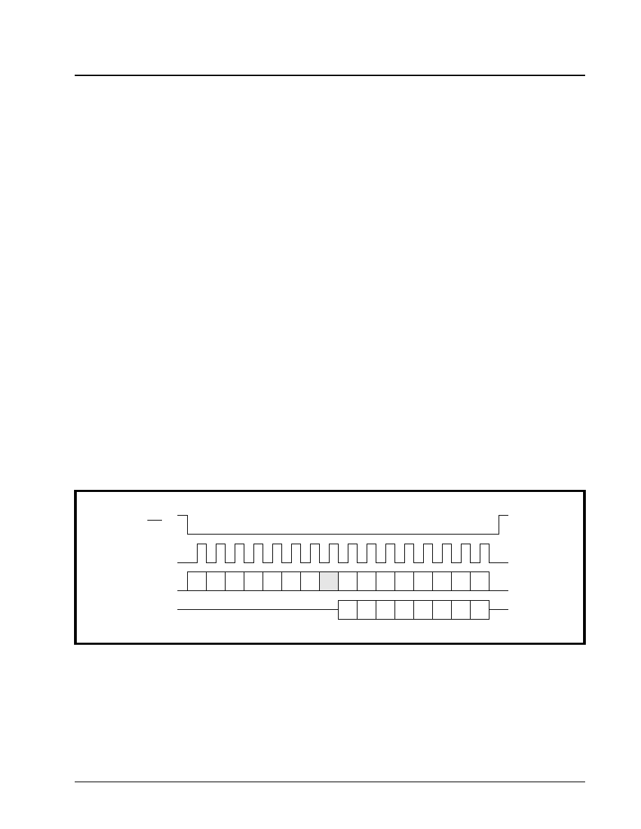
·Á
·Á
·Á
·Á
XRT83L30
ONE-CHANNEL T1/E1/J1 LH/SH TRANSCEIVER WITH CLOCK RECOVERY AND JITTER ATTENUATOR
PRELIMINARY
REV. P1.3.0
42
Bit 2 through 6:The five (5) Address Values (labeled A0, A1, A2, A3 and A4)
The next five rising edges of the SCLK signal, clock in the 5-bit address value for the Read or Write operation.
These five bits define the register address within XRT83L30 that the user has selected to read data from or
write data to. The address bits must be supplied to the SDI input in ascending order with LSB (Least Significant
Bit) first.
Bit 7:
(A5)
The next bit A5 must be set to "0" as shown in Figure 25.
Bit 8:
(A6)
The value of A6 is a "don't care".
Once the first eight bits have been written into the Serial interface, the subsequent action depends on the
whether the current operation is a "Read" or "Write" instruction.
Read Operation
With the last address bit "A4" written into the SDI input, the "Read" operation will proceed through an idle
period lasting two SCLK periods. On the rising edge of the 9th SCLK the serial data output (SDO) becomes
active (see Figure 25). At this point the user can begin reading the 8-bit data (D0 through D7) stored in the
interface register at address [A4,A3,A2,A1,A0], in ascending order (LSB first), on the falling edge of SCLK.
Write Operation
With the last address bit (A4) written into the SDI input, the "Write" operation will proceed through an idle
period lasting two SCLK periods. Prior to the rising edge of the 9th SCLK, the user must begin to apply the
eight bit data word to the SDI input. The Serial Interface will latch this data on the rising edge of SCLK. The
serial data (D0 through D7) should enter the SDI input in ascending order with the LSB first.
Serial Interface Register Description
The serial Interface consists of 32 8-bit register locations. The Microprocessor register address map and Bit
map are described in Table 16 and Table 17 respectively. The function of the individual bits are described in
Table 18 through Table 36.
F
IGURE
25. M
ICROPROCESSOR
S
ERIAL
I
NTERFACE
D
ATA
S
TRUCTURE
5
6
7
8
1
2
3
4
13
14
15
16
9
10
11
12
R/W
Ao
A1
A2
A3
A4
0
A6
D0
D1
D2
D3
D4
D5
D6
D7
D0
D1
D2
D3
D4
D5
D6
D7
CS
SCLK
SDI
S D O
High Z
High Z

XRT83L30
·Á
·Á
·Á
·Á
ONE-CHANNEL T1/E1/J1 LH/SH TRANSCEIVER WITH CLOCK RECOVERY AND JITTER ATTENUATOR
REV. P1.3.0
PRELIMINARY
43
T
ABLE
16: M
ICROPROCESSOR
R
EGISTER
A
DDRESS
R
EGISTER
N
UMBER
R
EGISTER
A
DDRESS
F
UNCTION
HEX
BINARY
0 - 18
0x00 - 0x12
00000 - 10010
Command and Control Registers
19 - 21
0x13 - 0x15
10011 - 10101
Reserved
22 - 29
0x16 - 0x1D
10110 - 11101
R/W registers reserved for testing purpose
30
0x1E
11110
Device "ID"
31
0x1F
11111
Device "Revision ID"
T
ABLE
17: M
ICROPROCESSOR
R
EGISTER
B
IT
M
AP
R
EG
. #
A
DDRESS
R
EG
.
T
YPE
B
IT
7
B
IT
6
B
IT
5
B
IT
4
B
IT
3
B
IT
2
B
IT
1
B
IT
0
Control Registers
0
00000
Hex 0x00
R/W
Reserved
Reserved
Reserved
EQC4
EQC3
EQC2
EQC1
EQC0
1
00001
Hex 0x01
R/W
RXTSEL
TXTSEL
TERSEL1
TERSEL0
JASEL1
JASEL0
JABW
FIFOS
2
00010
Hex 0x02
R/W
RXON
TXTEST2
TXTEST1
TXTEST0
TXON
LOOP2
LOOP1
LOOP0
3
00011
Hex 0x03
R/W
NLCDE1
NLCDE0
CODES
RXRES1
RXRES0
INSBPV
Reserved
TRATIO
4
00100
Hex 0x04
R/W
GIE
DMOIE
FLSIE
LCVIE
NLCDIE
AISDIE
RLOSIE
QRPDIE
5
00101
Hex 0x05
RO
Reserved
DMO
FLS
LCV
NLCD
AISD
RLOS
QRPD
6
00110
Hex 0x06
RUR
Reserved
DMOIS
FLSIS
LCVIS
NLCDIS
AISDIS
RLOSIS
QRPDIS
7
00111
Hex 0x07
RO
Reserved
Reserved
CLOS5
CLOS4
CLOS3
CLOS2
CLOS1
CLOS0
8
01000
Hex 0x08
R/W
X
B6S1
B5S1
B4S1
B3S1
B2S1
B1S1
B0S1
9
01001
Hex 0x09
R/W
X
B6S2
B5S2
B4S2
B3S2
B2S2
B1S2
B0S2
10
01010
Hex 0x0A
R/W
X
B6S3
B5S3
B4S3
B3S3
B2S3
B1S3
B0S3
11
01011
Hex 0x0B
R/W
X
B6S4
B5S4
B4S4
B3S4
B2S4
B1S4
B0S4
12
01100
Hex 0x0C
R/W
X
B6S5
B5S5
B4S5
B3S5
B2S5
B1S5
B0S5
13
01101
Hex 0x0D
R/W
X
B6S6
B5S6
B4S6
B3S6
B2S6
B1S6
B0S6
14
01110
Hex 0x0E
R/W
X
B6S7
B5S7
B4S7
B3S7
B2S7
B1S7
B0S7

·Á
·Á
·Á
·Á
XRT83L30
ONE-CHANNEL T1/E1/J1 LH/SH TRANSCEIVER WITH CLOCK RECOVERY AND JITTER ATTENUATOR
PRELIMINARY
REV. P1.3.0
44
15
01111
Hex 0x0F
R/W
X
B6S8
B5S8
B4S8
B3S8
B2S8
B1S8
B0S8
16
10000
Hex 0x10
R/W
SR/DR
ATAOS
RCLKE
TCLKE
DATAP
Reserved
Reserved
SRESET
17
10001
Hex 0x11
R/W
Reserved
CLKSEL2
CLKSEL1
CLKSEL0
MCLKRATE
RXMUTE
EXLOS
ICT
18
10010
Hex 0x12
R/W
GAUGE1
GAUGE0
TXONCNTL
TERCNTL
SL_1
SL_0
EQG_1
EQG_0
Reset = 0
Reset = 0
Reset = 0
Reset = 0
Reset = 0
Reset = 0
Reset = 0 Reset = 0
Unused Registers
19
10011
Hex 0x13
R/W
Reserved
Reserved
Reserved
Reserved
Reserved
Reserved
Reserved Reserved
20
10100
Hex 0x14
R/W
Reserved
Reserved
Reserved
Reserved
Reserved
Reserved
Reserved Reserved
21
10101
Hex 0x15
R/W
Reserved
Reserved
Reserved
Reserved
Reserved
Reserved
Reserved Reserved
Test Registers
22
10110
Hex 0x16
R/W
Test byte 0
23
10111
Hex 0x17
R/W
Test byte 1
24
11000
Hex 0x18
R/W
Test byte 2
25
11001
Hex 0x19
R/W
Test byte 3
26
11010
Hex 0x1A
R/W
Test byte 4
27
11011
Hex 0x1B
R/W
Test byte 5
28
11100
Hex 0x1C
R/W
Test byte 6
29
11101
Hex 0x1D
R/W
Test byte 7
ID Registers
30
11110
Hex 0x1E
DEVICE ID
F9
31
11111
Hex 0x1F
DEVICE "Revision ID"
T
ABLE
17: M
ICROPROCESSOR
R
EGISTER
B
IT
M
AP
R
EG
. #
A
DDRESS
R
EG
.
T
YPE
B
IT
7
B
IT
6
B
IT
5
B
IT
4
B
IT
3
B
IT
2
B
IT
1
B
IT
0

XRT83L30
·Á
·Á
·Á
·Á
ONE-CHANNEL T1/E1/J1 LH/SH TRANSCEIVER WITH CLOCK RECOVERY AND JITTER ATTENUATOR
REV. P1.3.0
PRELIMINARY
45
T
ABLE
18: M
ICROPROCESSOR
R
EGISTER
#0
BIT
DESCRIPTION
R
EGISTER
A
DDRESS
00000
F
UNCTION
R
EGISTER
T
YPE
R
ESET
V
ALUE
B
IT
#
N
AME
D7
Reserved
R/W
0
D6
Reserved
R/W
0
D5
Reserved
R/W
0
D4
EQC4
Equalizer Control bit 4: This bit together with EQC[3:0] are
used for controlling transmit pulse shaping, transmit line build-out
(LBO), receive monitoring and also T1 or E1 mode of operation.
See Table 5 for description of Equalizer Control bits.
R/W
0
D3
EQC3
Equalizer Control bit 3: See bit D4 description for function of
this bit
R/W
0
D2
EQC2
Equalizer Control bit 2: See bit D4 description for function of
this bit
R/W
0
D1
EQC1
Equalizer Control bit 1: See bit D4 description for function of
this bit
R/W
0
D0
EQC0
Equalizer Control bit 0: See bit D4 description for function of
this bit
R/W
0
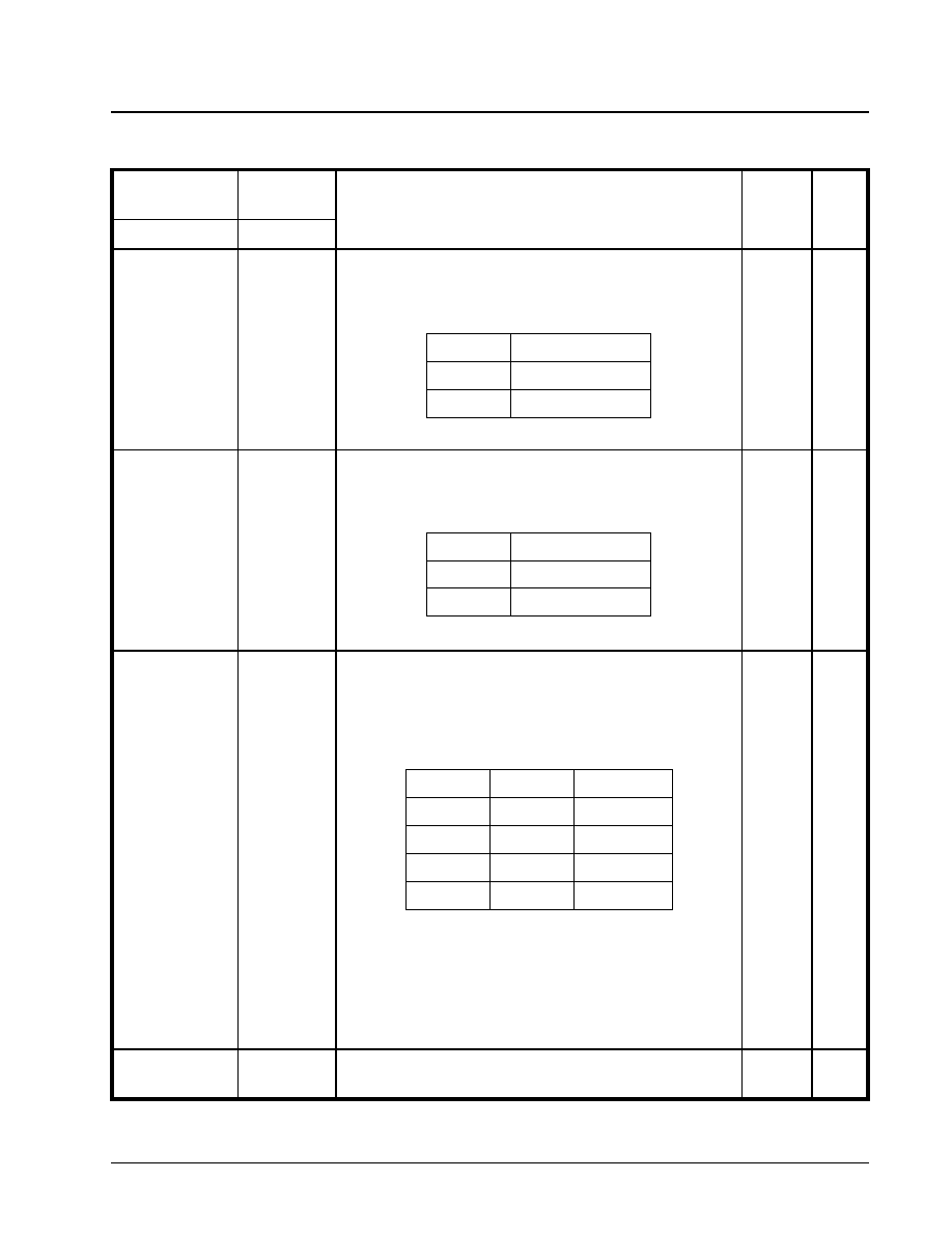
·Á
·Á
·Á
·Á
XRT83L30
ONE-CHANNEL T1/E1/J1 LH/SH TRANSCEIVER WITH CLOCK RECOVERY AND JITTER ATTENUATOR
PRELIMINARY
REV. P1.3.0
46
T
ABLE
19: M
ICROPROCESSOR
R
EGISTER
#1
BIT
DESCRIPTION
R
EGISTER
A
DDRESS
00001
F
UNCTION
R
EGISTER
T
YPE
R
ESET
V
ALUE
B
IT
#
N
AME
D7
RXTSEL
Receiver Termination Select: In Host mode, this bit is used to
select between the internal and external line termination modes
for the receiver according to the following table:
R/W
0
D6
TXTSEL
Transmit Termination Select: In Host mode, this bit is used to
select between the internal and external line termination modes
for the transmitter according to the following table:
R/W
0
D5
TERSEL1
Termination Impedance Select bit 1:
In the Host mode and in the internal termination mode (TXT-
SEL="1" and RXTSEL="1"), TERSEL[1:0] control the transmit
and receive termination impedance according to the following
table:
In the internal termination mode, the receiver termination of each
receiver is realized completely by internal resistors or by the
combination of internal and one fixed resistor (see description for
RXRES[1:0] bits).
In the internal termination mode, the transmitter output should be
AC coupled to the transformer.
R/W
0
D4
TERSEL0
Termination Impedance Select bit 0:
See description of bit D5 for the function of this bit.
R/W
0
RXTSEL
RX Termination
0
1
External
Internal
TXTSEL
TX Termination
0
1
External
Internal
0
1
1
0
1
1
0
0
100
110
75
120
Termination
TERSEL1
TERSEL0

XRT83L30
·Á
·Á
·Á
·Á
ONE-CHANNEL T1/E1/J1 LH/SH TRANSCEIVER WITH CLOCK RECOVERY AND JITTER ATTENUATOR
REV. P1.3.0
PRELIMINARY
47
D3
JASEL1
Jitter Attenuator select bit 1: The JASEL1 and JASEL0 bits are
used to disable or place the jitter attenuator in the transmit or
receive path.
R/W
0
D2
JASEL0
Jitter Attenuator select bit 0: See description of bit D3 for the
function of this bit.
R/W
0
D1
JABW
Jitter Attenuator Bandwidth Select:
In E1 mode, set this bit to "1" to select a 1.5Hz Bandwidth for the
Jitter Attenuator In E1 mode. The FIFO length will be automati-
cally set to 64 bits.
Set this bit to "0" to select 10Hz Bandwidth for the Jitter Attenua-
tor in E1 mode.
In T1 mode the Jitter Attenuator Bandwidth is permanently set to
3Hz, and the state of this bit has no effect on the Bandwidth.
R/W
0
D0
FIFOS
FIFO Size Select: See table of bit D1 above for the function of
this bit.
R/W
0
T
ABLE
19: M
ICROPROCESSOR
R
EGISTER
#1
BIT
DESCRIPTION
JASEL1
bit D3
JASEL0
bit D2
0
0
0
1
1
0
1
1
JA Path
JA Disabled
JA in Transmit Path
JA in Receive Path
JA in Receive Path
0
1
0
1
0
1
0
1
FIFOS_n
bit D0
0
0
1
1
0
0
1
1
JABW
bit D1
T1
T1
T1
T1
E1
E1
E1
E1
Mode
32
64
32
64
32
64
64
64
FIFO
Size
3
3
3
3
10
10
1.5
1.5
JA B-W
Hz
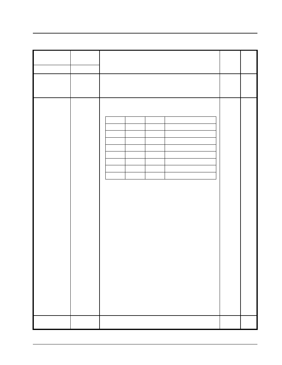
·Á
·Á
·Á
·Á
XRT83L30
ONE-CHANNEL T1/E1/J1 LH/SH TRANSCEIVER WITH CLOCK RECOVERY AND JITTER ATTENUATOR
PRELIMINARY
REV. P1.3.0
48
T
ABLE
20: M
ICROPROCESSOR
R
EGISTER
#2
BIT
DESCRIPTION
R
EGISTER
A
DDRESS
00010
F
UNCTION
R
EGISTER
T
YPE
R
ESET
V
ALUE
B
IT
#
N
AME
D7
RXON
Receiver ON: Writing a "1" into this bit location turns on the
Receive Section. Writing a "0" shuts off the Receiver Section. In
this mode, RTIP and RRING driver outputs will be tri-stated for
power reduction or redundancy applications. Default is "0", off.
R/W
0
D6
TXTEST2
Transmit Test Pattern bit 2: This bit together with TXTEST1 and
TXTEST0 are used to generate and transmit test patterns
according to the following table:
TDQRSS (Transmit/Detect Quasi-Random Signal): This con-
dition, when activated, enables Quasi-Random Signal Source
generation and detection. In a T1 system QRSS pattern is a 2
20
-
1 pseudo-random bit sequence (PRBS) with no more than 14
consecutive zeros. In a E1 system, QRSS is a 2
15
-1 PRBS pat-
tern.
TAOS (Transmit All Ones): Activating this condition enables the
transmission of an All Ones Pattern. TCLK must not be tied
"Low".
TLUC (Transmit Network Loop-Up Code): Activating this con-
dition enables the Network Loop-Up Code of "00001" to be trans-
mitted to the line. When Network Loop-Up code is being
transmitted, the XRT83L30 will ignore the Automatic Loop-Code
detection and Remote Loop-Back activation (NLCDE1 ="1",
NLCDE0 ="1", if activated) in order to avoid activating Remote
Digital Loop-Back automatically when the remote terminal
responds to the Loop-Back request.
TLDC (Transmit Network LOOP-Down Code): Activating this
condition enables the network Loop-Down Code of "001" to be
transmitted to the line.
R/W
0
D5
TXTEST1
Transmit Test pattern bit 1: See description of bit D6 for the
function of this bit.
R/W
0
0
1
1
0
1
1
0
0
0
0
0
1
0
0
0
Transmit Data
TAOS
TLUC
TLDC
Test Pattern
TXTEST1
TXTEST0
TXTEST2
1
0
1
1
1
1
0
1
1
TDQRSS
TDQRSS & INVQRSS
TDQRSS & INSBER
TDQRSS & INVQRSS & INSBER

XRT83L30
·Á
·Á
·Á
·Á
ONE-CHANNEL T1/E1/J1 LH/SH TRANSCEIVER WITH CLOCK RECOVERY AND JITTER ATTENUATOR
REV. P1.3.0
PRELIMINARY
49
D4
TXTEST0
Transmit Test Pattern bit 0: See description of bit D6 for the
function of this bit.
R/W
0
D3
TXON
Transmitter ON: Writing a "1" into this bit location turns on the
Transmit Section. A `0' in this bit location, shuts off the transmit-
ter. In this mode the TTIP and TRING driver outputs will be tri-
stated for power reduction or redundancy applications.
R/W
0
D2
LOOP2
Loop-Back control bit 2: This bit together with the LOOP1 and
LOOP0 bits control the Loop-Back modes of the chip according
to the following table:
R/W
0
D1
LOOP1
Loop-Back control bit 1: See description of bit D2 for the func-
tion of this bit.
R/W
0
D0
LOOP0
Loop-Back control bit 0: See description of bit D2 for the func-
tion of this bit.
R/W
0
T
ABLE
20: M
ICROPROCESSOR
R
EGISTER
#2
BIT
DESCRIPTION
LOOP2
0
1
1
1
1
LOOP1
X
0
0
1
1
LOOP0
X
0
1
0
1
Loop-Back Mode
No Loop-Back
Dual Loop-Back
Analog Loop-Back
Remote Loop-Back
Digital Loop-Back

·Á
·Á
·Á
·Á
XRT83L30
ONE-CHANNEL T1/E1/J1 LH/SH TRANSCEIVER WITH CLOCK RECOVERY AND JITTER ATTENUATOR
PRELIMINARY
REV. P1.3.0
50
T
ABLE
21: M
ICROPROCESSOR
R
EGISTER
#3
BIT
DESCRIPTION
R
EGISTER
A
DDRESS
00011
F
UNCTION
R
EGISTER
T
YPE
R
ESET
V
ALUE
B
IT
#
N
AME
D7
NLCDE1
Network Loop Code Detection Enable bit 1:
This bit together with NLCDE0, Control the Loop-Code detection
according to the following table:
When NLCDE1="0" and NCLDE0="1", or NLCDE1="1" and
NLCDE0="0", the chip is manually programed to monitor the
receive data for the Loop-Up or Loop-Down code respectively.
When the presence of the "00001" or "001" pattern is detected for
more than 5 seconds, the status of the NLCD bit is set to "1" and
if the NLCD interrupt is enabled an interrupt is initiated. The Host
has the option to control the Loop-Back function manually.
Setting the NLCDE1="1" and NLCDE0="1" enables the Auto-
matic Loop-Code detection and Remote-Loop-Back activation
mode. As this mode is initiated, the state of the NLCD interface
bit is reset to "0" and the chip is programmed to monitor the
receive data for the Loop-Up Code. If the "00001" pattern is
detected for longer than 5 seconds, the NLCD bit is set to "1",
Remote Loop-Back is activated and the chip is automatically pro-
gramed to monitor the receive data for the Loop-Down code. The
NLCD bit stays set even after the chip stops receiving the Loop-
Up code. The remote Loop-Back condition is removed when the
chip receives the Loop-Down code for more than 5 seconds or if
the Automatic Loop-Code detection mode is terminated.
R/W
R/W
0
0
D6
NLCDE0
Network Loop Code Detection Enable bit 0: See description
of bit D7 for the function of this bit.
R/W
0
D5
CODES
ENCODING and DECODING SELECT:
Writing a "0" to this bit selects HDB3 or B8ZS encoding and
decoding. Writing a "1" selects an AMI coding scheme.This bit is
only active when single-rail mode is selected.
R/W
0
NLCDE1
NLCDE0
Function
0
0
Disable Loop-Code
Detection
0
1
Detect Loop-Up Code in
Receive Data
1
1
Automatic Loop-Code
Detection
1
0
Detect Loop-Down Code in
Receive Data

XRT83L30
·Á
·Á
·Á
·Á
ONE-CHANNEL T1/E1/J1 LH/SH TRANSCEIVER WITH CLOCK RECOVERY AND JITTER ATTENUATOR
REV. P1.3.0
PRELIMINARY
51
D4
RXRES1
Receive External Resistor Control pin 1: In Host mode, this bit
along with the RXRES0 bit selects the value of the external
Receive fixed resistor according to the following table:
R/W
0
D3
RXRES0
Receive External Resistor Control bit 0: For function of this bit
see description of D4 the RXRES1 bit.
R/W
0
D2
INSBPV
Insert Bipolar Violation: When this bit transitions from "0" to
"1", a bipolar violation is inserted in the transmitted data stream.
Bipolar violation can be inserted either in the QRSS pattern, or
input data when operating in single-rail mode. The state of this bit
is sampled on the rising edge of TCLK.
N
OTE
: To ensure the insertion of a bipolar violation, a "0" should
be written in this bit location before writing a "1".
R/W
0
D1
Reserved
R/W
0
D0
TRATIO
Transformer Ratio Select: In the external termination mode,
writing a "1" to this bit selects a transformer ratio of 1:2 for the
transmitter. Writing a "0" sets the transmitter transformer ratio to
1: 2.45. In the internal termination mode the transmitter trans-
former ratio is permanently set to 1:2 and the state of this bit has
no effect.
R/W
0
T
ABLE
21: M
ICROPROCESSOR
R
EGISTER
#3
BIT
DESCRIPTION
Required Fixed External
RX Resistor
No External Fixed Resistor
60
52.5
37.5
RXRES0
0
1
0
1
RXRES1
0
0
1
1

·Á
·Á
·Á
·Á
XRT83L30
ONE-CHANNEL T1/E1/J1 LH/SH TRANSCEIVER WITH CLOCK RECOVERY AND JITTER ATTENUATOR
PRELIMINARY
REV. P1.3.0
52
T
ABLE
22: M
ICROPROCESSOR
R
EGISTER
#4
BIT
DESCRIPTION
R
EGISTER
A
DDRESS
00100
F
UNCTION
R
EGISTER
T
YPE
R
ESET
V
ALUE
B
IT
#
N
AME
D7
GIE
Global Interrupt Enable: Writing a "1" into this bit, globally
enables interrupt generation on the INT pin. Writing a "0" into this
bit, globally masks all interrupt requests.
R/W
0
D6
DMOIE
DMO Interrupt Enable: Writing a "1" to this bit enables DMO
interrupt generation, writing a "0" masks it.
R/W
0
D5
FLSIE
FIFO Limit Status Interrupt Enable: Writing a "1" to this bit
enables interrupt generation when the FIFO limit is within 3 bits,
writing a "0" to masks it.
R/W
0
D4
LCVIE
Line Code Violation Interrupt Enable: Writing a "1" to this bit
enables Line Code Violation interrupt generation, writing a "0"
masks it.
R/W
0
D3
NLCDIE
Network Loop-Code Detection Interrupt Enable: Writing a "1"
to this bit enables Network Loop-code detection interrupt genera-
tion, writing a "0" masks it.
R/W
0
D2
AISDIE
AIS Detection Interrupt Enable: Writing a "1" to this bit enables
Alarm Indication Signal detection interrupt generation, writing a
"0" masks it.
R/W
0
D1
RLOSIE
Receive Loss of Signal Interrupt Enable: Writing a "1" to this
bit enables Loss of Receive Signal interrupt generation, writing a
"0" masks it.
R/W
0
D0
QRPDIE
QRSS Pattern Detection Interrupt Enable: Writing a "1" to this
bit enables QRSS pattern detection interrupt generation, writing
a "0" masks it.
R/W
0

XRT83L30
·Á
·Á
·Á
·Á
ONE-CHANNEL T1/E1/J1 LH/SH TRANSCEIVER WITH CLOCK RECOVERY AND JITTER ATTENUATOR
REV. P1.3.0
PRELIMINARY
53
T
ABLE
23: M
ICROPROCESSOR
R
EGISTER
#5
BIT
DESCRIPTION
R
EGISTER
A
DDRESS
00101
F
UNCTION
R
EGISTER
T
YPE
R
ESET
V
ALUE
B
IT
#
N
AME
D7
Reserved
RO
0
D6
DMO
Driver Monitor Output: This bit is set to a "1" to indicate trans-
mit driver failure is detected. The value of this bit is based on the
current status of DMO. If the DMOIE bit is enabled, any transition
on this bit will generate an Interrupt.
RO
0
D5
FLS
FiFO Limit Status: This bit is set to a "1" to indicate that the jitter
attenuator read/write FIFO pointers are within +/- 3 bits. If the
FLSIE bit is enabled, any transition on this bit will generate an
Interrupt.
RO
0
D4
LCV
Line Code Violation: This bit is set to a "1" to indicate that the
receiver is currently detecting a Line Code Violation or an exces-
sive number of zeros in the B8ZS or HDB3 modes. If the LCVIE
bit is enabled, any transition on this bit will generate an Interrupt.
RO
0

·Á
·Á
·Á
·Á
XRT83L30
ONE-CHANNEL T1/E1/J1 LH/SH TRANSCEIVER WITH CLOCK RECOVERY AND JITTER ATTENUATOR
PRELIMINARY
REV. P1.3.0
54
D3
NLCD
Network Loop-Code Detection:
This bit operates differently in the Manual or the Automatic Net-
work Loop-Code detection modes.
In the Manual Loop-Code detection mode (NLCDE1 ="0" and
NLCDE0 ="1", or NLCDE1 ="1" and NLCDE0 ="0") this bit gets
set to "1" as soon as the Loop-Up ("00001") or Loop-Down
("001") code is detected in the receive data for longer than 5 sec-
onds. The NLCD bit stays in the "1" state for as long as the chip
detects the presence of the Loop-Code in the receive data and it
is reset to "0" as soon as it stops receiving it. In this mode if the
NLCD interrupt is enabled the chip will initiate an interrupt on
every transition of the NLCD.
When the Automatic Loop-Code detection mode (NLCDE1 ="1"
and NLCDE0 ="1") is initiated, the state of the NLCD interface bit
is reset to "0" and the chip is programmed to monitor the receive
input data for the Loop-Up Code. This bit is set to a "1" to indicate
that the Network Loop Code is detected for more than 5 seconds.
Simultaneously the Remote Loop-Back condition is automatically
activated and the chip is programmed to monitor the receive data
for the Network Loop-Down Code. The NLCD bit stays in the "1"
state for as long as the Remote Loop-Back condition is in effect
even if the chip stops receiving the Loop-Up Code. Remote
Loop-Back is removed if the chip detects the "001" pattern for
longer than 5 seconds in the receive data. Detecting the "001"
pattern also results in resetting the NLCD interface bit and initiat-
ing an interrupt provided the NLCD interrupt enable bit it active.
When programmed in the Automatic detection mode, the NLCD
interface bit stays "High" for the entire time the Remote Loop-
Back is active and initiates an interrupt anytime the status of the
NLCD bit changes. In this mode the host can monitor the state of
the NLCD bit to determine if the Remote Loop-Back is activated.
RO
0
D2
AISD
Alarm Indication Signal Detect: This bit is set to a "1" to indi-
cate All Ones Signal is detected by the receiver. The value of this
bit is based on the current status of Alarm Indication Signal
detector. If the AISDIE bit is enabled, any transition on this bit will
generate an Interrupt.
RO
0
D1
RLOS
Receive Loss of Signal: This bit is set to a "1" to indicate that
the receive input signal is lost. The value of this bit is based on
the current status of the receive input signal. If the RLOSIE bit is
enabled, any transition on this bit will generate an Interrupt.
RO
0
D0
QRPD
Quasi-random Pattern Detection: This bit is set to a "1" to indi-
cate the receiver is currently in synchronization with QRSS pat-
tern. The value of this bit is based on the current status of Quasi-
random pattern detector of. If the QRPDIE bit is enabled, any
transition on this bit will generate an Interrupt.
RO
0
T
ABLE
23: M
ICROPROCESSOR
R
EGISTER
#5
BIT
DESCRIPTION

XRT83L30
·Á
·Á
·Á
·Á
ONE-CHANNEL T1/E1/J1 LH/SH TRANSCEIVER WITH CLOCK RECOVERY AND JITTER ATTENUATOR
REV. P1.3.0
PRELIMINARY
55
T
ABLE
24: M
ICROPROCESSOR
R
EGISTER
#6
BIT
DESCRIPTION
R
EGISTER
A
DDRESS
00110
F
UNCTION
R
EGISTER
T
YPE
R
ESET
V
ALUE
B
IT
#
N
AME
D7
Reserved
RUR
0
D6
DMOIS
Driver Monitor Output Interrupt Status: This bit is set to a "1"
every time when DMO status has changed since last read.
RUR
0
D5
FLSIS
FIFO Limit Interrupt Status: This bit is set to a "1" every time
when FIFO Limit (Read/Write pointer with +/- 3 bits apart) status
has changed since last read.
RUR
0
D4
LCVIS
Line Code Violation Interrupt Status: This bit is set to a "1"
every time when LCV status has changed since last read.
RUR
0
D3
NLCDIS
Network Loop-Code Detection Interrupt Status: This bit is set
to a "1" every time when NLCD status has changed since last
read.
RUR
0
D2
AISDIS
AIS Detection Interrupt Status: This bit is set to a "1" every
time when AISD status has changed since last read.
RUR
0
D1
RLOSIS
Receive Loss of Signal Interrupt Status: This bit is set to a "1"
every time RLOS status has changed since last read.
RUR
0
D0
QRPDIS
Quasi-Random Pattern Detection Interrupt Status: This bit is
set to a "1" every time when QRPD status has changed since last
read.
RUR
0

·Á
·Á
·Á
·Á
XRT83L30
ONE-CHANNEL T1/E1/J1 LH/SH TRANSCEIVER WITH CLOCK RECOVERY AND JITTER ATTENUATOR
PRELIMINARY
REV. P1.3.0
56
T
ABLE
25: M
ICROPROCESSOR
R
EGISTER
#7
BIT
DESCRIPTION
R
EGISTER
A
DDRESS
00111
F
UNCTION
R
EGISTER
T
YPE
R
ESET
V
ALUE
B
IT
#
N
AME
D7
Reserved
RO
0
D6
Reserved
RO
0
D5
CLOS5
Cable Loss bit 5: CLOS[5:0] are the six bits receiver for selec-
tive equalizer setting which is also a binary word that represents
the cable attenuation indication within ±1dB. CLOS5 is the most
significant bit (MSB) and CLOS0 is the least significant bit (LSB).
RO
0
D4
CLOS4
Cable Loss bit 4: See description of D5 for function of this bit.
RO
0
D3
CLOS3
Cable Loss bit 3: See description of D5 for function of this bit.
RO
0
D2
CLOS2
Cable Loss bit 2: See description of D5 for function of this bit.
RO
0
D1
CLOS1
Cable Loss bit 1: See description of D5 for function of this bit.
RO
0
D0
CLOS0
Cable Loss bit 0: See description of D5 for function of this bit.
RO
0
T
ABLE
26: M
ICROPROCESSOR
R
EGISTER
#8
BIT
DESCRIPTION
R
EGISTER
A
DDRESS
01000
F
UNCTION
R
EGISTER
T
YPE
R
ESET
V
ALUE
B
IT
#
N
AME
D7
Reserved
R/W
0
D6-D0
B6S1 - B0S1 Arbitrary Transmit Pulse Shape, Segment 1
The shape of the transmitted pulse can be made user program-
mable by selecting "Arbitrary Pulse" mode, see Table 5. The arbi-
trary pulse is divided into eight time segments whose combined
duration is equal to one period of MCLK.
This 7 bit number represents the amplitude of the arbitrary pulse
during the first time segment. B6S1 -B0S1 is in signed magni-
tude format with B6S1 as the sign bit and B0S1 as the least sig-
nificant bit (LSB).
R/W
0

XRT83L30
·Á
·Á
·Á
·Á
ONE-CHANNEL T1/E1/J1 LH/SH TRANSCEIVER WITH CLOCK RECOVERY AND JITTER ATTENUATOR
REV. P1.3.0
PRELIMINARY
57
T
ABLE
27: M
ICROPROCESSOR
R
EGISTER
#9
BIT
DESCRIPTION
R
EGISTER
A
DDRESS
01001
F
UNCTION
R
EGISTER
T
YPE
R
ESET
V
ALUE
B
IT
#
N
AME
D7
Reserved
R/W
0
D6-D0
B6S2 - B0S2 Arbitrary Transmit Pulse Shape, Segment 2
The shape of the transmitted pulse can be made user program-
mable by selecting "Arbitrary Pulse" mode, see Table 5. The arbi-
trary pulse is divided into eight time segments whose combined
duration is equal to one period of MCLK.
This 7 bit number represents the amplitude of the arbitrary pulse
during the second time segment. B6S2 -B0S2 is in signed mag-
nitude format with B6S2 as the sign bit and B0S2 as the least
significant bit (LSB).
R/W
0
T
ABLE
28: M
ICROPROCESSOR
R
EGISTER
#10
BIT
DESCRIPTION
R
EGISTER
A
DDRESS
01010
F
UNCTION
R
EGISTER
T
YPE
R
ESET
V
ALUE
B
IT
#
N
AME
D7
Reserved
R/W
0
D6-D0
B6S3 - B0S3 Arbitrary Transmit Pulse Shape, Segment 3
The shape of the transmitted pulse can be made user program-
mable by selecting "Arbitrary Pulse" mode, see Table 5. The arbi-
trary pulse is divided into eight time segments whose combined
duration is equal to one period of MCLK.
This 7 bit number represents the amplitude of the arbitrary pulse
during the thrd time segment. B6S3 -B0S3 is in signed magni-
tude format with B6S3 as the sign bit and B0S3 as the least sig-
nificant bit (LSB).
R/W
0

·Á
·Á
·Á
·Á
XRT83L30
ONE-CHANNEL T1/E1/J1 LH/SH TRANSCEIVER WITH CLOCK RECOVERY AND JITTER ATTENUATOR
PRELIMINARY
REV. P1.3.0
58
T
ABLE
29: M
ICROPROCESSOR
R
EGISTER
#11
BIT
DESCRIPTION
R
EGISTER
A
DDRESS
01011
F
UNCTION
R
EGISTER
T
YPE
R
ESET
V
ALUE
B
IT
#
N
AME
D7
Reserved
R/W
0
D6-D0
B6S4 - B0S4 Arbitrary Transmit Pulse Shape, Segment 4
The shape of the transmitted pulse can be made user program-
mable by selecting "Arbitrary Pulse" mode, see Table 5. The arbi-
trary pulse is divided into eight time segments whose combined
duration is equal to one period of MCLK.
This 7 bit number represents the amplitude of the arbitrary pulse
during the fourth time segment. B6S4 -B0S4 is in signed magni-
tude format with B6S4 as the sign bit and B0S4 as the least sig-
nificant bit (LSB).
R/W
0
T
ABLE
30: M
ICROPROCESSOR
R
EGISTER
#12
BIT
DESCRIPTION
R
EGISTER
A
DDRESS
01100
F
UNCTION
R
EGISTER
T
YPE
R
ESET
V
ALUE
B
IT
#
N
AME
D7
Reserved
R/W
0
D6-D0
B6S5 - B0S5 Arbitrary Transmit Pulse Shape, Segment 5
The shape of the transmitted pulse can be made user program-
mable by selecting "Arbitrary Pulse" mode, see Table 5. The arbi-
trary pulse is divided into eight time segments whose combined
duration is equal to one period of MCLK.
This 7 bit number represents the amplitude of the arbitrary pulse
during the fith time segment. B6S5 -B0S5 is in signed magni-
tude format with B6S5 as the sign bit and B0S5 as the least sig-
nificant bit (LSB).
R/W
0

XRT83L30
·Á
·Á
·Á
·Á
ONE-CHANNEL T1/E1/J1 LH/SH TRANSCEIVER WITH CLOCK RECOVERY AND JITTER ATTENUATOR
REV. P1.3.0
PRELIMINARY
59
T
ABLE
31: M
ICROPROCESSOR
R
EGISTER
#13
BIT
DESCRIPTION
R
EGISTER
A
DDRESS
01101
F
UNCTION
R
EGISTER
T
YPE
R
ESET
V
ALUE
B
IT
#
N
AME
D7
Reserved
R/W
0
D6-D0
B6S6 - B0S6 Arbitrary Transmit Pulse Shape, Segment 6
The shape of the transmitted pulse can be made user program-
mable by selecting "Arbitrary Pulse" mode, see Table 5. The arbi-
trary pulse is divided into eight time segments whose combined
duration is equal to one period of MCLK.
This 7 bit number represents the amplitude of the arbitrary pulse
during the sixth time segment. B6S6 -B0S6 is in signed magni-
tude format with B6S6 as the sign bit and B0S6 as the least sig-
nificant bit (LSB).
R/W
0
T
ABLE
32: M
ICROPROCESSOR
R
EGISTER
#14
BIT
DESCRIPTION
R
EGISTER
A
DDRESS
01110
F
UNCTION
R
EGISTER
T
YPE
R
ESET
V
ALUE
B
IT
#
N
AME
D7
Reserved
R/W
0
D6-D0
B6S7 - B0S7 Arbitrary Transmit Pulse Shape, Segment 7
The shape of the transmitted pulse can be made user program-
mable by selecting "Arbitrary Pulse" mode, see Table 5. The arbi-
trary pulse is divided into eight time segments whose combined
duration is equal to one period of MCLK.
This 7 bit number represents the amplitude of the arbitrary pulse
during the seventh time segment. B6S7 -B0S7 is in signed mag-
nitude format with B6S7 as the sign bit and B0S7 as the least
significant bit (LSB).
R/W
0

·Á
·Á
·Á
·Á
XRT83L30
ONE-CHANNEL T1/E1/J1 LH/SH TRANSCEIVER WITH CLOCK RECOVERY AND JITTER ATTENUATOR
PRELIMINARY
REV. P1.3.0
60
T
ABLE
33: M
ICROPROCESSOR
R
EGISTER
#15
BIT
DESCRIPTION
R
EGISTER
A
DDRESS
01111
F
UNCTION
R
EGISTER
T
YPE
R
ESET
V
ALUE
B
IT
#
N
AME
D7
Reserved
R/W
0
D6-D0
B6S8 - B0S8 Arbitrary Transmit Pulse Shape, Segment 8
The shape of the transmitted pulse can be made user program-
mable by selecting "Arbitrary Pulse" mode, see Table 5. The arbi-
trary pulse is divided into eight time segments whose combined
duration is equal to one period of MCLK.
This 7 bit number represents the amplitude of the arbitrary pulse
during the eighth time segment. B6S8 -B0S8 is in signed magni-
tude format with B6S8 as the sign bit and B0S8 as the least sig-
nificant bit (LSB).
R/W
0

XRT83L30
·Á
·Á
·Á
·Á
ONE-CHANNEL T1/E1/J1 LH/SH TRANSCEIVER WITH CLOCK RECOVERY AND JITTER ATTENUATOR
REV. P1.3.0
PRELIMINARY
61
T
ABLE
34: M
ICROPROCESSOR
R
EGISTER
#16
BIT
DESCRIPTION
R
EGISTER
A
DDRESS
10000
N
AME
F
UNCTION
R
EGISTER
T
YPE
R
ESET
V
ALUE
B
IT
#
D7
SR/DR
Single-rail/Dual-rail Select: Writing a "1" to this bit configures
the XRT83L30 to operate in the Single-rail mode.
Writing a "0" configures the XRT83L30 to operate in Dual-rail
mode.
R/W
0
D6
ATAOS
Automatic Transmit All Ones Upon RLOS: Writing a "1" to this
bit enables the automatic transmission of All Ones data to the
line.
Writing a "0" disables this feature.
R/W
0
D5
RCLKE
Receive Clock Edge: Writing a "1" to this bit selects receive out-
put data to be updated on the negative edge of RCLK.
Writing a "0" selects data to be updated on the positive edge of
RCLK.
R/W
0
D4
TCLKE
Transmit Clock Edge: Writing a "0" to this bit selects transmit
data at TPOS/TDATA and TNEG to be sampled on the falling
edge of TCLK.
Writing a "1" selects the rising edge of the TCLK for sampling.
R/W
0
D3
DATAP
DATA Polarity: Writing a "0" to this bit selects transmit input and
receive output data of the XRT83L30 to be active "High".
Writing a "1" selects an active "Low" state.
R/W
0
D2
Reserved
R/W
0
D1
Reserved
R/W
0
D0
SRESET
Software Reset
µ
µ
µ
µ
P Registers: Writing a "1" to this bit longer
than 10
µ
s resets all internal state machines
R/W
0
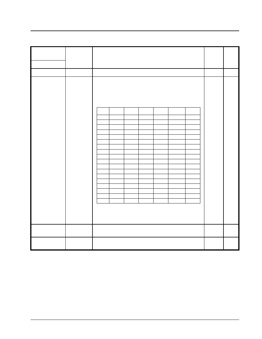
·Á
·Á
·Á
·Á
XRT83L30
ONE-CHANNEL T1/E1/J1 LH/SH TRANSCEIVER WITH CLOCK RECOVERY AND JITTER ATTENUATOR
PRELIMINARY
REV. P1.3.0
62
T
ABLE
35: M
ICROPROCESSOR
R
EGISTER
#17
BIT
DESCRIPTION
R
EGISTER
A
DDRESS
10001
N
AME
F
UNCTION
R
EGISTER
T
YPE
R
ESET
V
ALUE
B
IT
#
D7
Reserved
R/W
0
D6
CLKSEL2
Clock Select Inputs for Master Clock Synthesizer bit 2: In
Host mode, CLKSEL[2:0] are input signals to a programmable
frequency synthesizer that can be used to generate a master
clock from an external accurate clock source according to the fol-
lowing table:
In Hardware mode the state of these bits are ignored and the
master frequency PLL is controlled by the corresponding Hard-
ware pins.
R/W
0
D5
CLKSEL1
Clock Select inputs for Master Clock Synthesizer bit 1: See
description of bit D6 for function of this bit.
R/W
0
D4
CLKSEL0
Clock Select inputs for Master Clock Synthesizer bit 0: See
description of bit D6 for function of this bit.
R/W
0
2048
2048
2048
1544
M C L K E 1
k H z
8
16
16
56
8
56
64
64
128
256
256
128
2048
2048
1544
1544
M C L K T 1
k H z
1544
X
X
X
1544
X
X
X
X
X
X
X
2048
1544
2048
C L K O U T
k H z
1544
2048
1544
2048
1544
2048
1544
2048
1544
2048
1544
2048
1544
0
0
1
1
C L K S E L 0
0
1
1
0
0
0
1
1
0
1
1
0
0
0
0
0
C L K S E L 1
1
1
1
0
1
0
0
0
1
1
1
1
0
0
0
0
C L K S E L 2
0
0
0
1
0
1
1
1
1
1
1
1
0
1
0
0
0
0
1544
2048
X
X
2048
1544
0
1
0
1
M C L K R A T E
1
0
1
0
0
1
0
1
1
0
1
0
0
1

XRT83L30
·Á
·Á
·Á
·Á
ONE-CHANNEL T1/E1/J1 LH/SH TRANSCEIVER WITH CLOCK RECOVERY AND JITTER ATTENUATOR
REV. P1.3.0
PRELIMINARY
63
D3
MCLKRATE
Master Clock Rate Select: The state of this bit programs the
Master Clock Synthesizer to generate the T1/J1 or E1 clock. The
Master Clock Synthesizer will generate the E1 clock when
MCLKRATE = "0", and the T1/J1 clock when MCLKRATE = "1".
R/W
0
D2
RXMUTE
Receive Output Mute: Writing a "1" to this bit, mutes receive
outputs at RPOS/RDATA and RNEG/LCV pins to a "0" state.
N
OTE
: RCLK is not muted.
R/W
0
D1
EXLOS
Extended LOS: Writing a "1" to this bit extends the number of
zeros at the receive input before RLOS is declared to 4096 bits.
Writing a "0" reverts to the normal mode (175+75 bits for T1 and
32 bits for E1).
R/W
0
D0
ICT
In-Circuit-Testing: Writing a "1" to this bit configures all the out-
put pins of the chip in "High" impedance mode for In-Circuit-Test-
ing. Setting ICT bit to "1" is equivalent to connecting the
Hardware ICT pin to ground.
R/W
0
T
ABLE
36: M
ICROPROCESSOR
R
EGISTER
#18
BIT
DESCRIPTION
R
EGISTER
A
DDRESS
10010
N
AME
F
UNCTION
R
EGISTER
T
YPE
R
ESET
V
ALUE
B
IT
#
D7
GAUGE1
Wire Gauge Selector Bit 1
This bit along with bit D6 are used to select wire gauge size as
shown in the table below.
R/W
0
D6
GAUGE0
Wire Gauge Selector Bit 0
See bit D7.
R/W
0
D5
TXONCNTL
Transmit On Control.
In Host mode, setting this bit to "1" transfers the control of the
Transmit On/Off function to the TXON Hardware control pin.
N
OTE
: This provides a faster On/Off capability for redundancy
application.
R/W
0
D4
TERCNTL
Termination Control:
In Host mode, setting this bit to "1" transfers the control of the
RXTSEL to the RXTSEL Hardware control pin.
N
OTE
: This provides a faster On/Off capability for redundancy
application.
R/W
0
T
ABLE
35: M
ICROPROCESSOR
R
EGISTER
#17
BIT
DESCRIPTION
GAUGE1
0
1
1
0
GAUGE0
0
1
0
1
Wire Size
22 and 24 Gauge
26 Gauge
24 Gauge
22 Gauge

·Á
·Á
·Á
·Á
XRT83L30
ONE-CHANNEL T1/E1/J1 LH/SH TRANSCEIVER WITH CLOCK RECOVERY AND JITTER ATTENUATOR
PRELIMINARY
REV. P1.3.0
64
D3
SL_1
Slicer Level Control bit 1: This bit and bit D2 control the slic-
ing level for the slicer per the following table.
R/W
0
D2
SL_0
Slicer Level Control bit 0: See description bit D3.
R/W
0
D1
EQG_1
Equalizer Gain Control bit 1: This bit together with bit D0
control the gain of the equalizer as shown in the table below.
R/W
0
D0
EQG_0
Equalizer Gain Control bit 0: See description of bit D1.
R/W
0
T
ABLE
36: M
ICROPROCESSOR
R
EGISTER
#18
BIT
DESCRIPTION
SL_1
SL_0
0
0
0
1
1
0
1
1
Slicer Mode
Normal
Decrease by 5% from Normal
Increase by 5% from Normal
Normal
EQG_1
EQG_0
0
0
0
1
1
0
1
1
Equalizer Gain
Normal
Reduce Gain by 1 dB
Reduce Gain by 3 dB
Normal

XRT83L30
·Á
·Á
·Á
·Á
ONE-CHANNEL T1/E1/J1 LH/SH TRANSCEIVER WITH CLOCK RECOVERY AND JITTER ATTENUATOR
REV. P1.3.0
PRELIMINARY
65
ELECTRICAL CHARACTERISTICS
T
ABLE
37: A
BSOLUTE
M
AXIMUM
R
ATINGS
Storage Temperature...............-65∞C to +150∞C
Operating Temperature............. -40∞C to +85∞C
Supply Voltage............................-0.5V to +3.8V
Vin................................................-0.5 to +5.5V
T
ABLE
38: DC D
IGITAL
I
NPUT
AND
O
UTPUT
E
LECTRICAL
C
HARACTERISTICS
VDD=3.3V±5%, T
A
=25∞C,
UNLESS
OTHERWISE
SPECIFIED
P
ARAMETER
S
YMBOL
M
IN
T
YP
M
AX
U
NITS
Power Supply Voltage
VDD
3.13
3.3
3.46
V
Input High Voltage
V
IH
2.0
-
5.0
V
Input Low Voltage
V
IL
-0.5
-
0.8
V
Output High Voltage @ IOH = 2.0mA
V
OH
2.4
-
-
V
Output Low Voltage @IOL = 2.0mA
V
OL
-
-
0.4
V
Input Leakage Current (except Input pins
with Pull-up or Pull- down resistor).
I
L
-
-
±10
µ
A
Input Capacitance
C
I
-
5.0
-
pF
Output Load Capacitance
C
L
-
-
25
pF
T
ABLE
39: XRT83L30 P
OWER
C
ONSUMPTION
VDD=3.3V±5%, T
A
=25∞C,
UNLESS
OTHERWISE
SPECIFIED
M
ODE
S
UPPLY
V
OLTAGE
I
MPEDANCE
TERMINATION
R
ESISTOR
T
RANSFORMER
R
ATIO
T
YP
M
AX
U
NIT
T
EST
C
ONDITIONS
R
ECEIVER
T
RANSMITTER
E1
3.3V
75
6.2
2:1
1:2.42
150
210
mW
mW
50% "1's"
100% "1's"
E1
3.3V
75
9.1
2:1
1:2
150
180
mW
mW
50% "1's"
100% "1's"
E1
3.3V
120
6.2
2:1
1:2.42
140
145
mW
mW
50% "1's"
100% "1's"
E1
3.3V
120
9.1
2:1
1:2
130
135
mW
mW
50% "1's"
100% "1's"
T1
3.3V
100
3
2:1
1:2.42
200
285
mW
mW
50% "1's"
100% "1's"

·Á
·Á
·Á
·Á
XRT83L30
ONE-CHANNEL T1/E1/J1 LH/SH TRANSCEIVER WITH CLOCK RECOVERY AND JITTER ATTENUATOR
PRELIMINARY
REV. P1.3.0
66
T1
3.3V
100
3
2:1
1:2
230
310
mW
mW
50% "1's"
100% "1's"
----
3.3V
----
----
----
----
50
mW
Transmitter off
T
ABLE
40: E1 R
ECEIVER
E
LECTRICAL
C
HARACTERISTICS
VDD=3.3V±5%, T
A
= -40∞
TO
85∞C,
UNLESS
OTHERWISE
SPECIFIED
P
ARAMETER
M
IN
T
YP
M
AX
U
NIT
T
EST
C
ONDITIONS
Receiver loss of signal:
Number of consecutive zeros before
RLOS is set
Input signal level at RLOS
RLOS De-asserted
15
12.5
32
20
dB
% ones
Cable attenuation @1024KHz
ITU-G.775, ETSI 300 233
Receiver Sensitivity
(Short Haul with cable loss)
11
dB
With nominal pulse amplitude of 3.0V
for 120
and 2.37V for 75
applica-
tion. With -18dB interference signal
added.
Receiver Sensitivity
(Long Haul with cable loss)
0
43
dB
With nominal pulse amplitude of 3.0V
for 120
and 2.37V for 75
applica-
tion. With -18dB interference signal
added.
Input Impedance
13
k
Input Jitter Tolerance:
1 Hz
10kHz-100kHz
>64
0.4
UIpp
UIpp
ITU G.823
Recovered Clock Jitter
Transfer Corner Frequency
Peaking Amplitude
-
20
0.5
kHz
dB
ITU G.736
Jitter Attenuator Corner Frequency
(-3dB curve) (JABW=0)
(JABW=1)
-
10
1.5
-
Hz
Hz
ITU G.736
Return Loss:
51kHz - 102kHz
102kHz - 2048kHz
2048kHz - 3072kHz
14
20
16
-
-
dB
dB
dB
ITU-G.703
T
ABLE
39: XRT83L30 P
OWER
C
ONSUMPTION
VDD=3.3V±5%, T
A
=25∞C,
UNLESS
OTHERWISE
SPECIFIED
M
ODE
S
UPPLY
V
OLTAGE
I
MPEDANCE
TERMINATION
R
ESISTOR
T
RANSFORMER
R
ATIO
T
YP
M
AX
U
NIT
T
EST
C
ONDITIONS
R
ECEIVER
T
RANSMITTER

XRT83L30
·Á
·Á
·Á
·Á
ONE-CHANNEL T1/E1/J1 LH/SH TRANSCEIVER WITH CLOCK RECOVERY AND JITTER ATTENUATOR
REV. P1.3.0
PRELIMINARY
67
T
ABLE
41: T1 R
ECEIVER
E
LECTRICAL
C
HARACTERISTICS
VDD=3.3V±5%, T
A
= -40∞
TO
85∞C,
UNLESS
OTHERWISE
SPECIFIED
P
ARAMETER
M
IN
T
YP
M
AX
U
NIT
T
EST
C
ONDITIONS
Receiver loss of signal:
Number of consecutive zeros before
RLOS is set
Input signal level at RLOS
RLOS Clear
15
12.5
175
20
-
-
-
dB
% ones
Cable attenuation @772kHz
ITU-G.775, ETSI 300 233
Receiver Sensitivity
(Short Haul with cable loss)
12
dB
With nominal pulse amplitude of 3.0V
for 100
termination
Receiver Sensitivity
(Long Haul with cable loss)
Normal
Extended
0
0
-
36
45
dB
dB
With nominal pulse amplitude of 3.0V
for 100
termination
Input Impedance
13
-
k
Jitter Tolerance:
1Hz
10kHz - 100kHz
138
0.4
-
-
-
-
UIpp
AT&T Pub 62411
Recovered Clock Jitter
Transfer Corner Frequency
Peaking Amplitude
-
-
9.8
-
0.1
kHz
dB
TR-TSY-000499
Jitter Attenuator Corner Frequency
(-3dB curve)
-
3
Hz
AT&T Pub 62411
Return Loss:
51kHz - 102kHz
102kHz - 2048kHz
2048kHz - 3072kHz
-
-
-
20
25
25
-
-
-
dB
dB
dB
T
ABLE
42: E1 T
RANSMIT
R
ETURN
L
OSS
R
EQUIREMENT
F
REQUENCY
R
ETURN
L
OSS
G.703/CH-PTT
ETS 300166
51-102kHz
8dB
6dB
102-2048kHz
14dB
8dB
2048-3072kHz
10dB
8dB

·Á
·Á
·Á
·Á
XRT83L30
ONE-CHANNEL T1/E1/J1 LH/SH TRANSCEIVER WITH CLOCK RECOVERY AND JITTER ATTENUATOR
PRELIMINARY
REV. P1.3.0
68
T
ABLE
43: E1 T
RANSMITTER
E
LECTRICAL
C
HARACTERISTICS
VDD=3.3V±5%, T
A
= -40∞
TO
85∞C,
UNLESS
OTHERWISE
SPECIFIED
P
ARAMETER
M
IN
T
YP
M
AX
U
NIT
T
EST
C
ONDITIONS
AMI Output Pulse Amplitude:
75
Application
120
Application
2.13
2.70
2.37
3.0
2.60
3.30
V
V
Transformer with 1:2 ratio and 9.1
resistor in series with each end of pri-
mary.
Output Pulse Width
224
244
264
ns
Output Pulse Width Ratio
0.95
-
1.05
-
ITU-G.703
Output Pulse Amplitude Ratio
0.95
-
1.05
-
ITU-G.703
Jitter Added by the Transmitter Out-
put
-
0.025
0.05
UIpp
Broad Band with jitter free TCLK
applied to the input.
Output Return Loss:
51kHz -102kHz
102kHz-2048kHz
2048kHz-3072kHz
8
14
10
-
-
-
-
-
-
dB
dB
dB
ETSI 300 166, CHPTT
T
ABLE
44: T1 T
RANSMITTER
E
LECTRICAL
C
HARACTERISTICS
VDD=3.3V±5%, T
A
= -40∞
TO
85∞C,
UNLESS
OTHERWISE
SPECIFIED
P
ARAMETER
M
IN
T
YP
M
AX
U
NIT
T
EST
C
ONDITIONS
AMI Output Pulse Amplitude:
2.4
3.0
3.60
V
Tansformer with 1:2.45 ratio and mea-
sured at DSX-1
Output Pulse Width
338
350
362
ns
ANSI T1.102
Output Pulse Width Imbalance
-
-
20
-
ANSI T1.102
Output Pulse Amplitude Imbalance
-
-
+200
mV
ANSI T1.102
Jitter Added by the Transmitter Out-
put
-
0.025
0.05
UIpp
Broad Band with jitter free TCLK
applied to the input.
Output Return Loss:
51kHz -102kHz
102kHz-2048kHz
2048kHz-3072kHz
-
-
-
15
15
15
-
-
-
dB
dB
dB
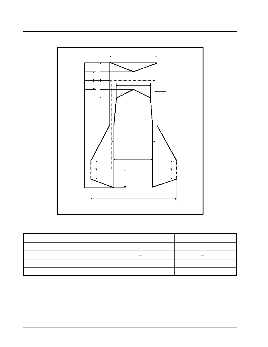
XRT83L30
·Á
·Á
·Á
·Á
ONE-CHANNEL T1/E1/J1 LH/SH TRANSCEIVER WITH CLOCK RECOVERY AND JITTER ATTENUATOR
REV. P1.3.0
PRELIMINARY
69
F
IGURE
26. ITU G.703 P
ULSE
T
EMPLATE
T
ABLE
45: T
RANSMIT
P
ULSE
M
ASK
S
PECIFICATION
Test Load Impedance
75
Resistive (Coax)
120
Resistive (twisted Pair)
Nominal Peak Voltage of a Mark
2.37V
3.0V
Peak voltage of a Space (no Mark)
0 + 0.237V
0 + 0.3V
Nominal Pulse width
244ns
244ns
Ratio of Positive and Negative Pulses Imbalance
0.95 to 1.05
0.95 to 1.05
10%
10%
10%
10%
10%
10%
269 ns
(244 + 25)
194 ns
(244 ≠ 50)
244 ns
219 ns
(244 ≠ 25)
488 ns
(244 + 244)
0%
50%
20%
V = 100%
Nominal pulse
Note ≠ V corresponds to the nominal peak value.
20%
20%
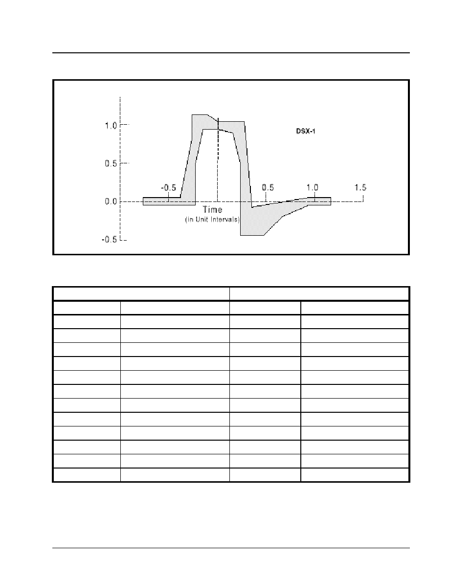
·Á
·Á
·Á
·Á
XRT83L30
ONE-CHANNEL T1/E1/J1 LH/SH TRANSCEIVER WITH CLOCK RECOVERY AND JITTER ATTENUATOR
PRELIMINARY
REV. P1.3.0
70
F
IGURE
27. DSX-1 P
ULSE
T
EMPLATE
(
NORMALIZED
AMPLITUDE
)
T
ABLE
46: DSX1 I
NTERFACE
I
SOLATED
P
ULSE
M
ASK
AND
C
ORNER
P
OINTS
M
INIMUM
CURVE
M
AXIMUM
CURVE
T
IME
(UI)
N
ORMALIZED
AMPLITUDE
T
IME
(UI)
N
ORMALIZED
AMPLITUDE
-0.77
-.05V
-0.77
.05V
-0.23
-.05V
-0.39
.05V
-0.23
0.5V
-0.27
.8V
-0.15
0.95V
-0.27
1.15V
0.0
0.95V
-0.12
1.15V
0.15
0.9V
0.0
1.05V
0.23
0.5V
0.27
1.05V
0.23
-0.45V
0.35
-0.07V
0.46
-0.45V
0.93
0.05V
0.66
-0.2V
1.16
0.05V
0.93
-0.05V
1.16
-0.05V
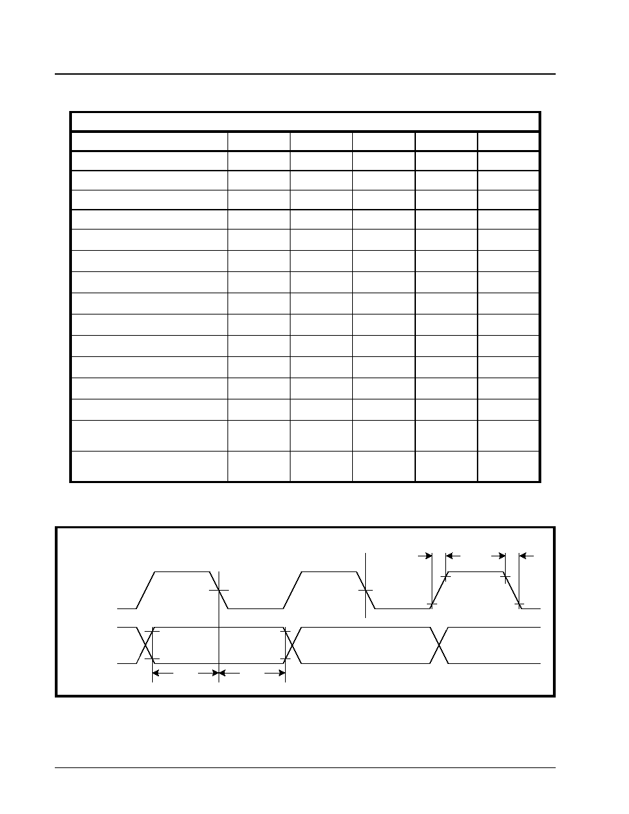
XRT83L30
·Á
·Á
·Á
·Á
ONE-CHANNEL T1/E1/J1 LH/SH TRANSCEIVER WITH CLOCK RECOVERY AND JITTER ATTENUATOR
REV. P1.3.0
PRELIMINARY
71
T
ABLE
47: AC E
LECTRICAL
C
HARACTERISTICS
(T
A
=25∞C, VDD=3.3V±5%,
UNLESS
OTHERWISE
SPECIFIED
)
P
ARAMETER
S
YMBOL
M
IN
T
YP
M
AX
U
NITS
E1 MCLK Clock Frequency
-
2.048
-
MHz
T1 MCLK Clock Frequency
-
1.544
-
MHz
MCLK Clock Duty Cycle
40
-
60
%
MCLK Clock Tolerance
-
±50
-
ppm
TCLK Duty Cycle
T
CDU
30
50
70
%
Transmit Data Setup Time
T
SU
50
-
-
ns
Transmit Data Hold Time
T
HO
30
-
-
ns
TCLK Rise Time(10%/90%)
T
CLKR
-
-
40
ns
TCLK Fall Time(90%/10%)
T
CLKF
-
-
40
ns
RCLK Duty Cycle
R
CDU
45
50
55
%
Receive Data Setup Time
R
SU
150
-
-
ns
Receive Data Hold Time
R
HO
150
-
-
ns
RCLK to Data Delay
R
DY
-
-
40
ns
RCLK Rise Time(10%/90%) with
25pF Loading.
RCLK
R
-
-
40
ns
RCLK Fall Time(90%/10%) with 25pF
Loading.
RCLK
F
40
ns
F
IGURE
28. T
RANSMIT
C
LOCK
AND
I
NPUT
D
ATA
T
IMING
TCLK
R
TCLK
F
TCLK
TPOS/TDATA
or
TNEG
T
SU
T
HO
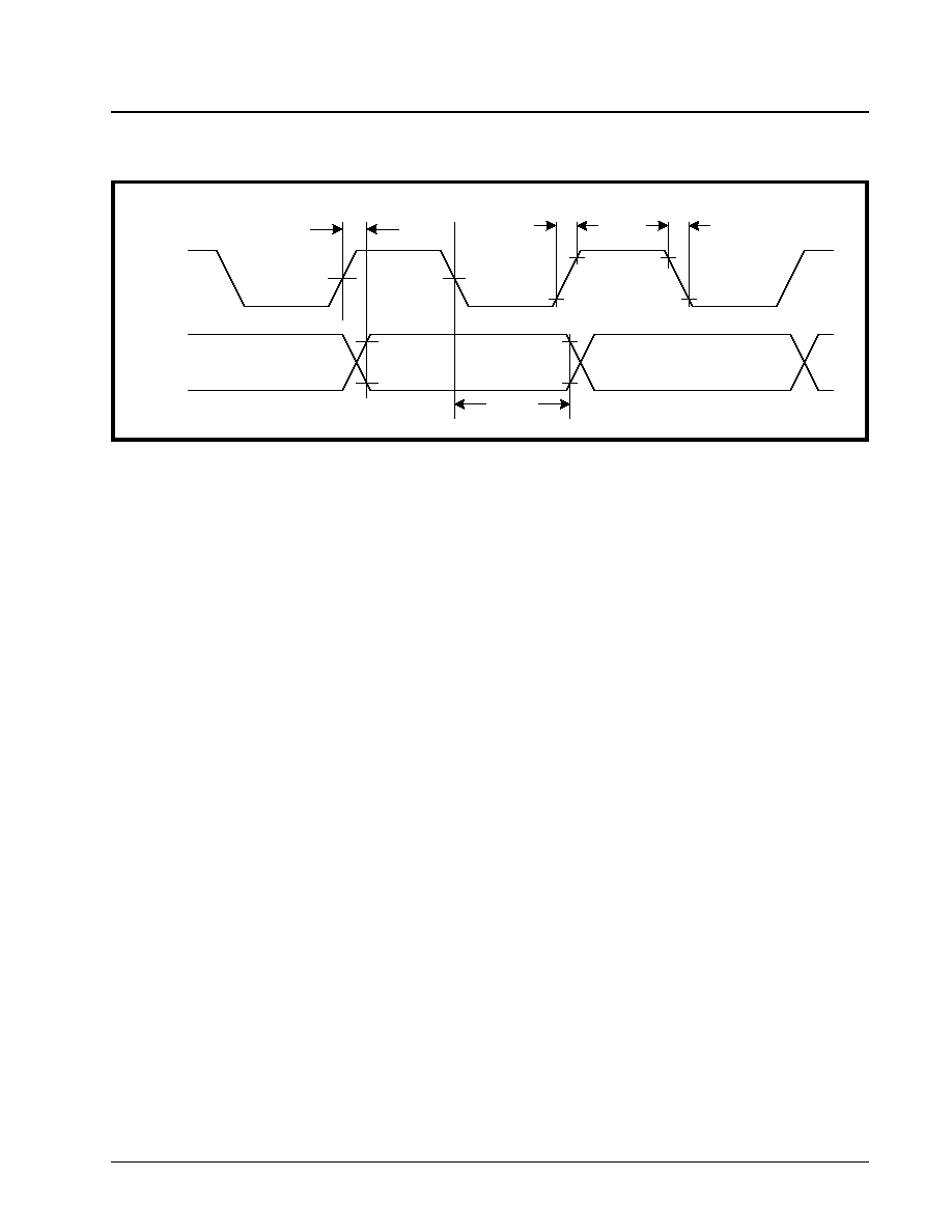
·Á
·Á
·Á
·Á
XRT83L30
ONE-CHANNEL T1/E1/J1 LH/SH TRANSCEIVER WITH CLOCK RECOVERY AND JITTER ATTENUATOR
PRELIMINARY
REV. P1.3.0
72
F
IGURE
29. R
ECEIVE
C
LOCK
AND
O
UTPUT
D
ATA
T
IMING
RCLK
R
RCLK
F
RCLK
RPOS
or
RNEG
R
DY
R
HO
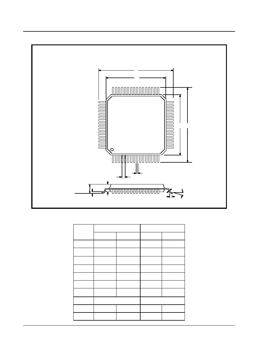
XRT83L30
·Á
·Á
·Á
·Á
SINGLE-CHANNEL T1/E1/J1 LH/SH TRANSCEIVER WITH CLOCK RECOVERY AND JITTER ATTENUATOR
REV. P1.3.0
PRELIMINARY
73
PACKAGE DIMENSIONS
64 LEAD THIN QUAD FLAT PACK
(10 X 10 X 1.4 MM TQFP)
REV. 3.00
Note: The control dimension is the millimeter column
INCHES
MILLIMETERS
SYMBOL
MIN
MAX
MIN
MAX
A
0.055
0.063
1.40
1.60
A
1
0.002
0.006
0.05
0.15
A
2
0.053
0.057
1.35
1.45
B
0.007
0.011
0.17
0.27
C
0.004
0.008
0.09
0.20
D
0.465
0.480
11.80
12.20
D
1
0.390
0.398
9.90
10.10
e
0.020 BSC
0.50 BSC
L
0.018
0.030
0.45
0.75
0
∞
7
∞
0
∞
7
∞
48
33
32
17
1
16
49
64
D
D
1
D
D
1
B
e
A
2
A
1
A
S eating Plane
L
C

·Á
·Á
·Á
·Á
XRT83L30
SINGLE-CHANNEL T1/E1/J1 LH/SH TRANSCEIVER WITH CLOCK RECOVERY AND JITTER ATTENUATOR
PRELIMINARY
REV. P1.3.0
74
ORDERING INFORMATION
REVISION HISTORY
Rev. A1.0.0 Advanced version.
Rev. P1.1.0 Preliminary release.
Rev. P1.2.0 Modified microprocessor tables, moved various functions. Added GHCI_n, SL_1, SL_0, EQG_1
EQG_0, GAUGE1 and GAUGE0 to Control Global Register 18. Separated Microprocessor description table by
register number. Moved absolute maximum and DC electrical characteristics before AC electrical characteris-
tics. Replaced TBD's in electrical ables. Reformated table of contents.
Rev. P1.2.1 Renamed FIFO pin to GAUGE, edited definition and edited defintion of JASEL[1:0] to reflect the
FIFO size is selected by the jitter attenuator select.
Rev. P1.2.2 Redefined bits D3, D2 and D0 of register 1, in combination these bits set the jitter attenuator path
and FIFO size.
Rev. P1.2.3 Added definitions to dual function pins in the pin description section.
Rev P1.2.4 Added JABW, JASEL1 and JASEL0 table in pin list and Jitter attenuator section. Corrected typos in
features, figures 7, 8, 9 and 11. Added Jitter attenuator tables in microprocessor register tables.
Rev. P1.2.5 Table 18, 23, 24, 25 change GCHIE to GIE, GHCI and GCHIS to Reserved. Corrected package
outline drawing.
Rev. P1.2.6 TERCNTL (pin 46) function removed. Bit 7 of Microprocessor Register #2 was INSBER, is now re-
served. Bit 1 of Microprocessor Register #3 was INVQRSS, is now reserved. New description for bits D6 - D0
in Tables 27 - 34 Microprocessor Registers.
Rev. P1.2.7 Expanded information on Receive Redundancy. 2 tables and 1 figure.
Rev. P1.2.8 Edited section on RLOS
Rev. P1.2.9 Removed TERCNTL from block diagram. Edit EQC[4:0] to be input only on block diagram. Cor-
rected RXMUTE, TCLK, JABW, MCKLE1, CLKSEL [2:0], RXTSEL, TERSEL[1:0], RXRES[1:0], ATAOS, NLCD
in the pin descriptions section. Replaced the Functional Description section. Edits to Table 18: Microproces-
sor Register Bit Map, Table 21: Microprocessor Register #2 Bit Description, Table 35: Microprocessor Register
#16 Bit Description
Rev. P1.3.0 Table 35: Microprocessor Register #17 Bit Description, edit E1 clock MCLKRATE= "0" and T1/J1
clock MCLKRATE="1" .
P
ART
#
P
ACKAGE
O
PERATING
TEMPERATURE
R
ANGE
XRT83L30IV
64 Pin TQFP
-40
o
C to +85
o
C
T
HERMAL
I
NFORMATION
Theta - J
A
= 38∞ C/W
Theta J
C
= 7∞ C/W

XRT83L30
·Á
·Á
·Á
·Á
SINGLE-CHANNEL T1/E1/J1 LH/SH TRANSCEIVER WITH CLOCK RECOVERY AND JITTER ATTENUATOR
PRELIMINARY
REV. P1.3.0
75
NOTICE
EXAR Corporation reserves the right to make changes to the products contained in this publication in order
to improve design, performance or reliability. EXAR Corporation assumes no responsibility for the use of
any circuits described herein, conveys no license under any patent or other right, and makes no represen-
tation that the circuits are free of patent infringement. Charts and schedules contained here in are only for
illustration purposes and may vary depending upon a user's specific application. While the information in
this publication has been carefully checked; no responsibility, however, is assumed for inaccuracies.
EXAR Corporation does not recommend the use of any of its products in life support applications where
the failure or malfunction of the product can reasonably be expected to cause failure of the life support sys-
tem or to significantly affect its safety or effectiveness. Products are not authorized for use in such applica-
tions unless EXAR Corporation receives, in writing, assurances to its satisfaction that: (a) the risk of injury
or damage has been minimized; (b) the user assumes all such risks; (c) potential liability of EXAR Corpo-
ration is adequately protected under the circumstances.
Copyright 2003 EXAR Corporation
Datasheet May 2003.
Reproduction, in part or whole, without the prior written consent of EXAR Corporation is prohibited.
NOTES