Document Outline
- GENERAL DESCRIPTION
- Pin Descriptions
- 1.0 Microprocessor Interface Block
- Table 3: µC/µP Selection Table
- 1.1 Channel Selection within the Framer
- 1.2 The Microprocessor Interface Block Signal
- 1.3 Interfacing the XRT84L38 to the Local µC/ µP via the Microprocessor Interface Block
- 1.3.1 Interfacing the Framer to the Microprocessor over an 8 bit wide bi-directional Data Bus
- 1.3.2 Data Access Modes
- Figure 4. Intel µP Interface signals during Programmed I/O Read Operation
- Figure 5. Intel µP Interface Signals, during Programmed I/O Write Operation
- Figure 6. Motorola µP Interface signals, during a Programmed I/O Read Operation
- Figure 7. Motorola µP Interface signal during Programmed I/O Write Operation
- Figure 8. Intel µP Interface Signals, during the Initial Read Operation of a Burst Cycle
- Figure 9. Intel µP Interface Signals, during subsequent Read Operations of a Burst I/O Cycle
- Figure 10. Intel µP Interface signals, during the Initial Write Operation of a Burst Cycle
- Figure 11. µP Interface Signals, during subsequent Write Operations of a Burst I/O Cycle
- Figure 12. Motorola µP Interface Signals, during the Initial Read Operation of a Burst Cycle
- Figure 13. Motorola µP Interface Signals, during subsequent Read Operations of a Burst I/O Cycle
- Figure 14. Motorola µP Interface signals, during the Initial Write Operation of a Burst Cycle
- Figure 15. Motorola µP Interface Signals, during subsequent Write Operations of a Burst I/O Cycle
- 1.4 DMA Read/Write Operations
- 1.5 Memory and Register Map
- 1.6 Description of the Control Registers
- Register summary
- 1.7 The Interrupt Structure within the Framer
- 2.0 The E1 Framing Structure
- 3.0 The DS1 Framing Structure
- 4.0 Clock Distribution System
- 5.0 Transmit Terminal Serial Input �Interface
- 6.0 Transmit Overhead Input Interface
- 7.0 The Transmit Framer Block
- 8.0 Receive Framer
- 9.0 Receive Overhead Output Interface
- 10.0 Receive Output Interface
- 11.0 Transmit LIU Interface
- 12.0 Receive LIU Interface
- 13.0 LIU Controller Block
- 14.0 Data Link Controller

Exar
Corporation 48720 Kato Road, Fremont CA, 94538
∑
(510) 668-7000
∑
FAX (510) 668-7017
∑
www.exar.com
·Á
·Á
·Á
·Á
PRELIMINARY
XRT84L38
OCTAL T1/E1/J1 FRAMER
DECEMBER 2001
REV. P1.0.1
GENERAL DESCRIPTION
The XRT84L38 is an eight-channel 1.544 Mbit/s or
2.048 Mbit/s DS1/E1/J1 framing controller. The
XRT84L38 contains an integrated DS1/E1/J1 framer
which provides DS1/E1/J1 framing and error accumu-
lation in accordance with ANSI/ITU_T specifications.
Each framer has its own framing synchronizer and
transmit-receive slip buffers, and can be independent-
ly enabled or disabled as required and can be config-
ured to frame to the common DS1/E1/J1 signal for-
mats
Each Framer block contains its own Transmit and Re-
ceive T1/E1/J1 Framing function. The Transmit HDLC
controller encapsulates contents of the Transmit
HDLC buffers into LAPD Message frames. The Re-
ceive HDLC controller extracts payload content of Re-
ceive LAPD Message frames from the incoming T1/
E1/J1 data stream and writes it into the Receive
HDLC buffer. Each framer also contains a Transmit
and Overhead Data Input port, which permits Data
Link Terminal Equipment direct access to the out-
bound T1/E1/J1 frames Likewise, a Receive Over-
head output data port permits Data Link Terminal
Equipment direct access to the Data Link bits of the
inbound T1/E1/J1 frames.
The XRT84L38 fully meets all of the latest T1/E1/J1
specifications: ANSI T1/E1.107-1988, ANSI T1/
E1.403-1995, ANSI T1/E1.231-1993, ANSI T1/
E1.408-1990, AT&T TR 62411 (12-90) TR54016, and
ITU G-703, G.704, G706 and G.733, AT&T Pub.
43801, and ETS 300 011, 300 233, JT G.703, JT
G.704, JT G706, I.431. Extensive test and diagnostic
functions include Loop-backs, Boundary scan, Pseu-
do Random bit sequence (PRBS) test pattern gener-
ation, Performance Monitor, Bit Error Rate (BER)
meter, forced error insertion, and LAPD unchannel-
ized data payload processing according to ITU-T
standard Q.921.
Applications and Features (next page)
F
IGURE
1. XRT84L38 8-
CHANNEL
DS1 (T1/E1/J1) F
RAMER
X R T 8 3 L 38
X R T8 4 L 38
;0&+#742(4#/,8
H o s t M o d e
T x 1
R x 8
TPO S
TN E G
TC L K 1
R PO S
R N E G
R C L K1
TxPO S
TxN E G
TxLineC LK
R xP O S
R xN E G
R xL in eC LK
L o c a l P C M
H ig h w a y
8 D S 1 /E 1
C h an n els
1 .5 4 4 /2 .0 4 8 M H z
B a ck P lan e
1 .5 4 4 -
1 6 .3 8 4
M b it/s
C o n fig u ra tio n , C o n tro l &
S ta t u s M o n ito r
T x E n c o d e r
L IU
In te rfa c e
P e rfo rm a n c e
M o n ito r
L IU
&
L o o p b a c k
C o n tro l
M ic ro p ro c e s s o r
In te rfa c e
D [7:0]
A [6:0]
7
W R
A LE _A S
R D
R D Y_D TA C K
C ha nne l
S elect
3
8
R x 1
T x 8
8
8
8
8
8
L B
L L B
H D L C (L AP D )
C o n tro lle r &
9 6 -b yte B u ffe r
R x S e ria l
D a ta O u t
1 o f 8 -c h an n e ls
R x O ve rh e a d O u t
8
8
In te rrupt
2 -F ra m e
S lip B u ffe r
E la s tic S to re
8 kH z sync
O SC
T x O v e rh e a d In
2 -F ra m e
S lip B u f fe r
E la s tic S to re
T x s e ria l
c lo c k
R x s e ria l
c lo c k
T x
F ra m e r
P R B S
G e n e ra to r
&
An a ly s e r
R x
F ra m e r
E x tern al D ata
L in k C o n tro lle r
R x E n c o d e r
L IU
In te rfa c e
S ig n a lin g
& Ala rm s
T x S e ria l
D a ta In
µ
µ
µ
µ
P
In te rfa c e
L in e S id e
S ys te m (T e rm in al) S id e
ST
-
B
U
S
D M A
In te rfa c e
In te l/M o to ro la
µ
µ
µ
µ
P
M e m o r y
T w is te d
P a ir
T w is te d
P a ir
∑
∑
∑
∑
∑
∑
∑
∑
∑
J T AG

XRT84L38
·Á
·Á
·Á
·Á
OCTAL T1/E1/J1 FRAMER
REV. P1.0.1
PRELIMINARY
2
APPLICATIONS
∑ High-Density T1/E1/J1 interfaces for Multiplexers,
Switches, LAN Routers and Digital Modems
∑ SONET/SDH terminal or Add/Drop multiplexers
(ADMs)
∑ T1/E1/J1 add/drop multiplexers (MUX)
∑ Channel Service Units (CSUs): T1/E1/J1 and Frac-
tional T1/E1/J1
∑ Digital Access Cross-connect System (DACs)
∑ Digital Cross-connect Systems (DCS)
∑ Frame Relay Switches and Access Devices
(FRADS)
∑ ISDN Primary Rate Interfaces (PRA)
∑ PBXs and PCM channel bank
∑ T3 channelized access concentrators and M13
MUX
∑ Wireless base stations
∑ ATM equipment with integrated DS1 interfaces
∑ Multichannel DS1 Test Equipment
∑ T1/E1/J1 Performance Monitoring
∑ Voice over packet gateways
∑ Routers
FEATURES
∑ Eight independent, full duplex DS1 Tx and Rx
Framers
∑ Two 512-bit (two-frame) elastic store, PCM frame
slip buffers (FIFO) on TX and Rx provide up to
8.192 MHz asynchronous back plane connections
with jitter and wander attenuation
∑ Supports input PCM and signaling data at 1.544,
2.048, 4.096 and 8.192 Mbits. Also supports 4-
channel multiplexed 12.352/16.384 (HMVIP/H.100)
Mbit/s on the back plane bus
∑ Programmable output clocks for Fractional T1/E1/
J1
∑ Supports Channel Associated Signaling (CAS)
∑ Supports Common Channel Signalling (CCS)
∑ Supports ISDN Primary Rate Interface (ISDN PRI)
signaling
∑ Extracts and inserts robbed bit signaling (RBS)
∑ Integrated HDLC controller with two 96-byte Trans-
mit HDLC buffers and two 96-byte Receive HDLC
buffers
∑ Timeslot assignable HDLC
∑ V5.1 Interface
∑ 8-bit Intel/Motorola
µ
P and MIPS Power PC inter-
faces for configuration, control and status monitor-
ing
∑ Parallel search algorithm for fast frame synchroni-
zation
∑ Wide choice of T1 framing structures: D4, ESF,
SLCÆ96, TIDM and N-Frame (non-framing)
∑ Direct access to D and E channels for fast transmis-
sion of data link information
∑ PRBS and QRSS generation and detection
∑ Programmable Interrupt output pin
∑ Supports programmed I/O, Burst and DMA modes
of Read-Write access
∑ Each framer block encodes and decodes the T1/
E1/J1 Frame serial data into and from the Single-
rail or Dual-rail (B8ZS) format
∑ Dual or single rail line side digital PCM inputs
∑ Detects and forces Red (SAI), Yellow (RAI) and
Blue (AIS) Alarms
∑ Detects OOF, LOF, LOS errors and COFA condi-
tions
∑ Loopbacks: Local (LLB) and Line remote (LB)
∑ Facilitates Inverse Multiplexing for ATM
∑ Performance monitor with one second polling
∑ Boundary scan (IEEE 1149.1) JTAG test port
∑ Accepts external 8kHz Sync reference
∑ 3.3V CMOS operation with 5V tolerant inputs
∑ 388-pin BGA package with ≠40
∞
C to +85
∞
C opera-
tion
∑ Direct Interface to Exar's XRT83L38 (Octal) LIU
ORDERING INFORMATION
P
ART
N
UMBER
P
ACKAGE
O
PERATING
T
EMPERATURE
R
ANGE
XRT84L38IB
388 Pin Plastic Ball Grid Array
-40
∞
C to +85
∞
C

·Á
·Á
·Á
·Á
XRT84L38
OCTAL T1/E1/J1 FRAMER
PRELIMINARY
REV. P1.0.1
3
F
IGURE
2. P
IN
O
UT
OF
THE
XRT84L38 T
OP
V
IEW
(
SEE
PIN
LIST
FOR
NAMES
AND
FUNCTION
)
A
B
C
D
E
F
G
H
J
K
L
M
N
P
R
T
U
V
W
Y
AA
AB
AC
AD
AE
AF
21
22
19
20
23
24
25
26
1
2
3
4
5
6
7
8
17
18
13
14
15
16
9
10
11
12
XRT84L38
(See pin list for pin names and function)
Top View
AC
1
AF
1
AE
1
AD
1
A1
D4
C1
B1
E1
F1
G1
H1
J1
K1
L1
M1
AA
1
AB
1
U1
V1
W1
Y1
N1
P1
R1
T1
A
26
D
23
D
26
AC
23
AC
26
AF
26
L
26
T
26
L
23
T
23
L
24
T
24
L
25
T
25
AC
4
D4
L4
L2
T2
L3
T3
T4
V3
V1
V1
V1
V1
G
V1
V1
G
G
G
G
G
G
G
G
G
G
G
V2
G
G
V1
V1
V3
V3
V3
V3
V3
V2
V2
V2
V2
V2
V2
V2

XRT84L38
·Á
·Á
·Á
·Á
OCTAL T1/E1/J1 FRAMER
REV. P1.0.1
PRELIMINARY
I
TABLE OF CONTENTS
GENERAL DESCRIPTION ................................................................................................. 1
Figure 1. XRT84L38 8-channel DS1 (T1/E1/J1) Framer ................................................................... 1
A
PPLICATIONS
.............................................................................................................................................. 2
F
EATURES
.................................................................................................................................................... 2
ORDERING INFORMATION ............................................................................................................... 2
Figure 2. Pin Out of the XRT84L38 Top View (see pin list for names and function) .................... 3
TABLE OF CONTENTS ....................................................................................................... I
PIN DESCRIPTIONS .......................................................................................................... 8
T
RANSMIT
S
ERIAL
D
ATA
I
NPUT
...................................................................................................................... 8
O
VERHEAD
I
NTERFACE
............................................................................................................................... 17
R
ECEIVE
S
ERIAL
D
ATA
O
UTPUT
.................................................................................................................. 19
R
ECEIVE
D
ECODER
L
IU
I
NTERFACE
............................................................................................................. 26
T
RANSMIT
E
NCODER
L
IU
I
NTERFACE
........................................................................................................... 26
T
IMING
....................................................................................................................................................... 27
L
IU
C
ONTROL
............................................................................................................................................. 28
JTAG ........................................................................................................................................................ 29
M
ICROPROCESSOR
I
NTERFACE
.................................................................................................................... 30
G
ROUND
P
INS
............................................................................................................................................ 33
P
OWER
S
UPPLY
P
INS
................................................................................................................................. 33
N
O
C
ONNECT
P
INS
..................................................................................................................................... 34
E
LECTRICAL
C
HARACTERISTICS
................................................................................................................... 35
A
BSOLUTE
M
AXIMUMS
................................................................................................................................ 35
DC E
LECTRICAL
C
HARACTERISTICS
............................................................................................................ 35
T
ABLE
2: XRT84L38 P
OWER
C
ONSUMPTION
...................................................................................... 36
1.0 Microprocessor Interface Block ............................................................................................................ 37
1.1 C
HANNEL
S
ELECTION
WITHIN
THE
F
RAMER
............................................................................................ 37
T
ABLE
3: µC/µP S
ELECTION
T
ABLE
..................................................................................................... 37
T
ABLE
4: C
HANNEL
S
ELECTION
........................................................................................................... 38
Figure 3. Simplified Block Diagram of the Microprocessor Interface Block .............................. 38
1.2 T
HE
M
ICROPROCESSOR
I
NTERFACE
B
LOCK
S
IGNAL
............................................................................... 38
T
ABLE
5: XRT84L38 M
ICROPROCESSOR
I
NTERFACE
S
IGNALS
THAT
EXHIBIT
CONSTANT
ROLES
IN
BOTH
THE
I
NTEL
AND
M
OTOROLA
M
ODES
................................................................................................ 39
T
ABLE
6: I
NTEL
MODE
: M
ICROPROCESSOR
I
NTERFACE
S
IGNALS
........................................................... 39
T
ABLE
7: M
OTOROLA
M
ODE
: M
ICROPROCESSOR
I
NTERFACE
S
IGNALS
.................................................. 40
1.3 I
NTERFACING
THE
XRT84L38
TO
THE
L
OCAL
µC/µP
VIA
THE
M
ICROPROCESSOR
I
NTERFACE
B
LOCK
....... 40
1.3.1 Interfacing the Framer to the Microprocessor over an 8 bit wide bi-directional Data Bus ......... 40
1.3.2 Data Access Modes .................................................................................................................. 41
Figure 4. Intel µP Interface signals during Programmed I/O Read Operation ............................ 42
Figure 5. Intel µP Interface Signals, during Programmed I/O Write Operation .......................... 43
Figure 6. Motorola µP Interface signals, during a Programmed I/O Read Operation ................ 44
Figure 7. Motorola µP Interface signal during Programmed I/O Write Operation ...................... 45
Figure 8. Intel µP Interface Signals, during the Initial Read Operation of a Burst Cycle .......... 46
Figure 9. Intel µP Interface Signals, during subsequent Read Operations of a Burst I/O Cycle ...
47
Figure 10. Intel µP Interface signals, during the Initial Write Operation of a Burst Cycle ........ 48
Figure 11. µP Interface Signals, during subsequent Write Operations of a Burst I/O Cycle .... 49
Figure 12. Motorola µP Interface Signals, during the Initial Read Operation of a Burst Cycle 50
Figure 13. Motorola µP Interface Signals, during subsequent Read Operations of a Burst I/O Cy-
cle ......................................................................................................................................... 51
Figure 14. Motorola µP Interface signals, during the Initial Write Operation of a Burst Cycle . 52
Figure 15. Motorola µP Interface Signals, during subsequent Write Operations of a Burst I/O Cy-
cle ......................................................................................................................................... 53

·Á
·Á
·Á
·Á
XRT84L38
OCTAL T1/E1/J1 FRAMER
PRELIMINARY
REV. P1.0.1
II
1.4 DMA R
EAD
/W
RITE
O
PERATIONS
.......................................................................................................... 53
DMA-0 Write DMA Interface ............................................................................................................................. 53
Figure 16. DMA Mode for the XRT84L38 and a Microprocessor ................................................. 54
1.5 M
EMORY
AND
R
EGISTER
M
AP
.............................................................................................................. 54
1.5.1 Memory Mapped I/O Indirect Addressing ................................................................................. 54
T
ABLE
8: A
DDRESS
M
AP
..................................................................................................................... 55
1.6 D
ESCRIPTION
OF
THE
C
ONTROL
R
EGISTERS
......................................................................................... 56
1.6.1 List of Registers ........................................................................................................................ 56
R
EGISTER
SUMMARY
.................................................................................................................................. 56
T
ABLE
9: R
EGISTER
S
UMMARY
............................................................................................................ 56
1.6.2 Register Descriptions ............................................................................................................... 60
T
ABLE
10: C
LOCK
S
ELECT
R
EGISTER
E1 M
ODE
.................................................................................. 60
T
ABLE
11: C
LOCK
S
ELECT
R
EGISTER
- T1 M
ODE
................................................................................ 61
T
ABLE
12: L
INE
I
NTERFACE
C
ONTROL
R
EGISTER
E1 M
ODE
................................................................. 62
T
ABLE
13: L
INE
I
NTERFACE
C
ONTROL
R
EGISTER
T1 M
ODE
................................................................. 63
T
ABLE
14: L
INE
C
ONTROL
R
EGISTER
.................................................................................................. 64
T
ABLE
15: LIU A
CCESS
R
EGISTER
1 ................................................................................................... 64
T
ABLE
16: LIU A
CCESS
R
EGISTER
2 ................................................................................................... 65
T
ABLE
17: LIU P
OLL
R
EGISTER
1 ....................................................................................................... 65
T
ABLE
18: LIU P
OLL
R
EGISTER
2 ....................................................................................................... 65
T
ABLE
19: F
RAMING
S
ELECT
R
EGISTER
-E1 M
ODE
............................................................................... 66
T
ABLE
20: F
RAMING
S
ELECT
R
EGISTER
-T1 M
ODE
............................................................................... 67
T
ABLE
21: A
LARM
G
ENERATION
R
EGISTER
- E1 M
ODE
........................................................................ 68
T
ABLE
22: A
LARM
G
ENERATION
R
EGISTER
-T1 M
ODE
......................................................................... 69
T
ABLE
23: S
YNCHRONIZATION
MUX R
EGISTER
- E1 M
ODE
.................................................................. 70
T
ABLE
24: S
YNCHRONIZATION
MUX R
EGISTER
- T1 M
ODE
.................................................................. 71
T
ABLE
25: T
RANSMIT
S
IGNALING
AND
D
ATA
L
INK
S
ELECT
R
EGISTER
- E1 M
ODE
................................. 72
T
ABLE
26: T
RANSMIT
S
IGNALING
AND
D
ATA
L
INK
S
ELECT
R
EGISTER
- T1 M
ODE
................................. 73
T
ABLE
27: F
RAMING
C
ONTROL
R
EGISTER
E1 M
ODE
............................................................................ 74
T
ABLE
28: F
RAMING
C
ONTROL
R
EGISTER
T1 M
ODE
............................................................................ 75
T
ABLE
29: R
ECEIVE
S
IGNALING
& D
ATA
L
INK
S
ELECT
R
EGISTER
- E1 M
ODE
....................................... 76
T
ABLE
30: R
ECEIVE
S
IGNALING
& D
ATA
L
INK
S
ELECT
R
EGISTER
(RS&DLSR) T1 M
ODE
.................... 77
T
ABLE
31: S
IGNALING
C
HANGE
R
EGISTER
0 - T1 M
ODE
...................................................................... 77
T
ABLE
32: S
IGNALING
C
HANGE
R
EGISTER
0 - E1 M
ODE
...................................................................... 78
T
ABLE
33: S
IGNALING
C
HANGE
R
EGISTER
1 ........................................................................................ 78
T
ABLE
34: S
IGNALING
C
HANGE
R
EGISTER
2 ........................................................................................ 78
T
ABLE
35: S
IGNALING
C
HANGE
R
EGISTER
3 ........................................................................................ 79
T
ABLE
36: R
ECEIVE
N
ATIONAL
B
ITS
R
EGISTER
.................................................................................... 79
T
ABLE
37: R
ECEIVE
E
XTRA
B
ITS
R
EGISTER
......................................................................................... 80
T
ABLE
38: D
ATA
L
INK
C
ONTROL
R
EGISTER
......................................................................................... 81
T
ABLE
39: T
RANSMIT
D
ATA
L
INK
B
YTE
C
OUNT
R
EGISTER
................................................................... 82
T
ABLE
40: R
ECEIVE
D
ATA
L
INK
B
YTE
C
OUNT
R
EGISTER
..................................................................... 82
T
ABLE
41: S
LIP
B
UFFER
C
ONTROL
R
EGISTER
..................................................................................... 83
T
ABLE
42: FIFO L
ATENCY
R
EGISTER
.................................................................................................. 83
T
ABLE
43: DMA 0 (W
RITE
) C
ONFIGURATION
R
EGISTER
....................................................................... 84
T
ABLE
44: DMA 1 (R
EAD
) C
ONFIGURATION
R
EGISTER
........................................................................ 85
T
ABLE
45: I
NTERRUPT
C
ONTROL
R
EGISTER
......................................................................................... 85
T
ABLE
46: T
RANSMIT
I
NTERFACE
C
ONTROL
R
EGISTER
- E1 M
ODE
....................................................... 86
T
ABLE
47: T
RANSMIT
I
NTERFACE
C
ONTROL
R
EGISTER
- T1 M
ODE
....................................................... 87
T
ABLE
48: R
ECEIVE
I
NTERFACE
C
ONTROL
R
EGISTER
(RICR) - E1 M
ODE
............................................. 88
T
ABLE
49: R
ECEIVE
I
NTERFACE
C
ONTROL
R
EGISTER
(RICR) - T1 M
ODE
............................................. 89
T
ABLE
50: DS1 T
EST
R
EGISTER
......................................................................................................... 90
T
ABLE
51: L
OOPBACK
C
ODE
C
ONTROL
R
EGISTER
............................................................................... 91
T
ABLE
52: T
RANSMIT
L
OOPBACK
C
ODER
R
EGISTER
............................................................................ 91
T
ABLE
53: T
RANSMIT
L
OOPBACK
A
CTIVATION
C
ODE
R
EGISTER
........................................................... 92

XRT84L38
·Á
·Á
·Á
·Á
OCTAL T1/E1/J1 FRAMER
REV. P1.0.1
PRELIMINARY
III
T
ABLE
54: T
RANSMIT
L
OOPBACK
D
EACTIVATION
C
ODE
R
EGISTER
........................................................ 92
T
ABLE
55: T
RANSMIT
S
A
S
ELECT
R
EGISTER
........................................................................................ 93
T
ABLE
56: T
RANSMIT
S
A
A
UTO
C
ONTROL
R
EGISTER
1 ........................................................................ 94
T
ABLE
57: C
ONDITIONS
ON
R
ECEIVE
SIDE
W
HEN
TSACR1
BITS
A
RE
ENABLED
.................................... 94
T
ABLE
58: T
RANSMIT
S
A
A
UTO
C
ONTROL
R
EGISTER
2 ........................................................................ 95
T
ABLE
59: C
ONDITIONS
ON
R
ECEIVE
SIDE
W
HEN
TSACR1
BITS
ENABLED
............................................ 95
T
ABLE
60: T
RANSMIT
S
A
4 R
EGISTER
................................................................................................... 95
T
ABLE
61: T
RANSMIT
S
A
5 R
EGISTER
................................................................................................... 96
T
ABLE
62: T
RANSMIT
S
A
6 R
EGISTER
................................................................................................... 96
T
ABLE
63: T
RANSMIT
S
A
7 R
EGISTER
................................................................................................... 96
T
ABLE
64: T
RANSMIT
S
A
8 R
EGISTER
................................................................................................... 96
T
ABLE
65: R
ECEIVE
S
A
4 R
EGISTER
..................................................................................................... 97
T
ABLE
66: R
ECEIVE
S
A
5 R
EGISTER
..................................................................................................... 97
T
ABLE
67: R
ECEIVE
S
A
6 R
EGISTER
..................................................................................................... 97
T
ABLE
68: R
ECEIVE
S
A
7 R
EGISTER
..................................................................................................... 97
T
ABLE
69: R
ECEIVE
S
A
8 R
EGISTER
..................................................................................................... 97
T
ABLE
70: T
RANSMIT
C
HANNEL
C
ONTROL
R
EGISTER
0
TO
31 E1 M
ODE
.............................................. 98
T
ABLE
71: T
RANSMIT
C
HANNEL
C
ONTROL
R
EGISTER
0
TO
31 T1 M
ODE
............................................... 99
T
ABLE
72: U
SER
C
ODE
R
EGISTER
0
TO
31 ........................................................................................ 100
T
ABLE
73: T
RANSMIT
S
IGNALING
C
ONTROL
R
EGISTER
X
- E1 M
ODE
.................................................. 100
T
ABLE
74: T
RANSMIT
S
IGNALING
C
ONTROL
R
EGISTER
X
- T1 M
ODE
................................................... 101
T
ABLE
75: R
ECEIVE
C
HANNEL
C
ONTROL
R
EGISTER
X
(RCCR 0-31) - E1 M
ODE
................................ 102
T
ABLE
76: R
ECEIVE
C
HANNEL
C
ONTROL
R
EGISTER
X
(RCCR 0-23) - T1 M
ODE
................................. 103
T
ABLE
77: R
ECEIVE
U
SER
C
ODE
R
EGISTER
X
(RUCR 0-31) .............................................................. 103
T
ABLE
78: R
ECEIVE
S
IGNALING
C
ONTROL
R
EGISTER
X
(RSCR) (0-31) .............................................. 104
T
ABLE
79: R
ECEIVE
S
UBSTITUTION
S
IGNALING
R
EGISTER
(RSSR) E1 M
ODE
..................................... 104
T
ABLE
80: R
ECEIVE
S
UBSTITUTION
S
IGNALING
R
EGISTER
(RSSR) T1 M
ODE
..................................... 105
T
ABLE
81: R
ECEIVE
S
IGNALING
A
RRAY
R
EGISTER
0
TO
31 ................................................................ 105
T
ABLE
82: PMON T1/E1 R
ECEIVE
L
INE
C
ODE
(
BIPOLAR
) V
IOLATION
C
OUNTER
................................. 105
T
ABLE
83: PMON T1/E1 R
ECEIVE
L
INE
C
ODE
(
BIPOLAR
) V
IOLATION
C
OUNTER
................................. 105
T
ABLE
84: PMON T1/E1 R
ECEIVE
F
RAMING
A
LIGNMENT
B
IT
E
RROR
C
OUNTER
................................. 106
T
ABLE
85: PMON T1/E1 R
ECEIVE
F
RAMING
A
LIGNMENT
B
IT
E
RROR
C
OUNTER
................................. 106
T
ABLE
86: PMON T1/E1 R
ECEIVE
S
EVERELY
E
RRORED
F
RAME
C
OUNTER
........................................ 106
T
ABLE
87: PMON T1/E1 R
ECEIVE
CRC-4 B
LOCK
E
RROR
C
OUNTER
- MSB ...................................... 106
T
ABLE
88: PMON T1/E1 R
ECEIVE
CRC-4 B
LOCK
E
RROR
C
OUNTER
- LSB ....................................... 107
T
ABLE
89: PMON T1/E1 R
ECEIVE
F
AR
-E
ND
BL
OCK
E
RROR
C
OUNTER
- MSB .................................. 107
T
ABLE
90: PMON T1/E1 R
ECEIVE
F
AR
E
ND
B
LOCK
E
RROR
C
OUNTER
.............................................. 107
T
ABLE
91: PMON T1/E1 R
ECEIVE
S
LIP
C
OUNTER
............................................................................. 108
T
ABLE
92: PMON T1/E1 R
ECEIVE
L
OSS
OF
F
RAME
C
OUNTER
........................................................... 108
T
ABLE
93: PMON T1/E1 R
ECEIVE
C
HANGE
OF
F
RAME
A
LIGNMENT
C
OUNTER
................................... 108
T
ABLE
94: PMON LAPD T1/E1 F
RAME
C
HECK
S
EQUENCE
E
RROR
C
OUNTER
................................... 108
T
ABLE
95: T1/E1 PRBS B
IT
E
RROR
C
OUNTER
MSB ......................................................................... 109
T
ABLE
96: T1/E1 PRBS B
IT
E
RROR
C
OUNTER
LSB ......................................................................... 109
T
ABLE
97: T1/E1 T
RANSMIT
S
LIP
C
OUNTER
...................................................................................... 109
T
ABLE
98: B
LOCK
I
NTERRUPT
S
TATUS
R
EGISTER
.............................................................................. 110
T
ABLE
99: B
LOCK
I
NTERRUPT
E
NABLE
R
EGISTER
.............................................................................. 111
T
ABLE
100: A
LARM
& E
RROR
I
NTERRUPT
S
TATUS
R
EGISTER
............................................................. 111
T
ABLE
101: A
LARM
& E
RROR
I
NTERRUPT
E
NABLE
R
EGISTER
- E1 M
ODE
.......................................... 113
T
ABLE
102: A
LARM
& E
RROR
I
NTERRUPT
E
NABLE
R
EGISTER
-T1 M
ODE
............................................ 114
T
ABLE
103: F
RAMER
I
NTERRUPT
S
TATUS
R
EGISTER
E1 M
ODE
........................................................... 115
T
ABLE
104: F
RAMER
I
NTERRUPT
S
TATUS
R
EGISTER
T1 M
ODE
........................................................... 116
T
ABLE
105: F
RAMER
I
NTERRUPT
E
NABLE
R
EGISTER
E1 M
ODE
.......................................................... 117
T
ABLE
106: F
RAMER
I
NTERRUPT
E
NABLE
R
EGISTER
T1 M
ODE
.......................................................... 118
T
ABLE
107: D
ATA
L
INK
S
TATUS
R
EGISTER
........................................................................................ 119

·Á
·Á
·Á
·Á
XRT84L38
OCTAL T1/E1/J1 FRAMER
PRELIMINARY
REV. P1.0.1
IV
T
ABLE
108: D
ATA
L
INK
I
NTERRUPT
E
NABLE
R
EGISTER
...................................................................... 120
T
ABLE
109: S
LIP
B
UFFER
I
NTERRUPT
S
TATUS
R
EGISTER
(SBSR) ..................................................... 121
T
ABLE
110: S
LIP
B
UFFER
I
NTERRUPT
E
NABLE
R
EGISTER
(SBIER) .................................................... 121
T
ABLE
111: R
ECEIVE
L
OOPBACK
C
ODE
I
NTERRUPT
AND
S
TATUS
R
EGISTER
(RLCISR) ...................... 122
T
ABLE
112: R
ECEIVE
L
OOPBACK
C
ODE
I
NTERRUPT
E
NABLE
R
EGISTER
(RLCIER) ............................. 122
T
ABLE
113: R
ECEIVE
SA I
NTERRUPT
R
EGISTER
(RSAIR) .................................................................. 123
T
ABLE
114: R
ECEIVE
SA I
NTERRUPT
E
NABLE
R
EGISTER
(RSAIER) .................................................. 124
1.7 T
HE
I
NTERRUPT
S
TRUCTURE
WITHIN
THE
F
RAMER
.............................................................................. 125
T
ABLE
115: L
IST
OF
THE
P
OSSIBLE
C
ONDITIONS
THAT
CAN
G
ENERATE
I
NTERRUPTS
,
IN
EACH
F
RAMER
125
T
ABLE
116: A
DDRESS
OF
THE
B
LOCK
I
NTERRUPT
S
TATUS
R
EGISTERS
............................................... 126
T
ABLE
117: B
LOCK
I
NTERRUPT
S
TATUS
R
EGISTER
............................................................................ 127
T
ABLE
118: B
LOCK
I
NTERRUPT
E
NABLE
R
EGISTER
........................................................................... 128
1.7.1 Configuring the Interrupt System, at the Framer Level ........................................................... 129
T
ABLE
119: I
NTERRUPT
C
ONTROL
R
EGISTER
..................................................................................... 129
2.0 The E1 Framing Structure .................................................................................................................... 131
2.1 T
HE
S
INGLE
E1 F
RAME
...................................................................................................................... 131
Figure 17. Single E1 Frame Diagram ........................................................................................... 131
Timeslot 0 ....................................................................................................................................................... 131
Timeslot 0 octets within FAS frames .............................................................................................................. 131
T
ABLE
120: B
IT
F
ORMAT
OF
T
IMESLOT
0
OCTET
WITHIN
A
FAS E1 F
RAME
........................................ 131
Bit 0--Si (International Bit) ............................................................................................................................. 131
T
ABLE
121: B
IT
F
ORMAT
OF
T
IMESLOT
0
OCTET
WITHIN
A
N
ON
-FAS E1 F
RAME
................................ 132
Bit 0--Si (International Bit) ............................................................................................................................. 132
Bit 1--Fixed at "1" .......................................................................................................................................... 132
Bit 2--A (FAS Frame Yellow Alarm Bit) ......................................................................................................... 132
Bit 3 through 7--Sa4≠Sa8 (National Bits) ...................................................................................................... 132
2.2 T
HE
E1 M
ULTI
-
FRAME
S
TRUCTURES
................................................................................................... 132
2.2.1 The CRC Multi-frame Structure .............................................................................................. 132
T
ABLE
122: B
IT
F
ORMAT
OF
ALL
T
IMESLOT
0
OCTETS
WITHIN
A
CRC M
ULTI
-
FRAME
.......................... 133
2.2.2 CAS Multi-Frames and Channel Associated Signaling .......................................................... 133
Figure 18. Frame/Byte Format of the CAS Multi-Frame Structure ............................................ 134
Figure 19. E1 Frame Format ......................................................................................................... 135
3.0 The DS1 Framing Structure ................................................................................................................. 136
Figure 20. T1 Frame Format ......................................................................................................... 136
3.1 T1 S
UPER
F
RAME
F
ORMAT
(SF) ........................................................................................................ 136
Figure 21. T1 Superframe PCM Format ....................................................................................... 137
T
ABLE
123: S
UPERFRAME
F
ORMAT
................................................................................................... 137
3.2 T1 E
XTENDED
S
UPERFRAME
F
ORMAT
................................................................................................. 138
Figure 22. T1 Extended Superframe Format ............................................................................... 138
T
ABLE
124: E
XTENDED
S
UPERFRAME
F
ORMAT
.................................................................................. 139
3.3 SLC 96 F
ORMAT
(SLC) ..................................................................................................................... 140
T
ABLE
125: SLC 96 F
S
B
IT
C
ONTENTS
............................................................................................. 140
4.0 Clock Distribution System ................................................................................................................... 141
R
ECEIVE
S
ECTION
.................................................................................................................................... 141
T
RANSMIT
S
ECTION
.................................................................................................................................. 141
CSS-- C
LOCK
S
OURCE
S
ELECT
(T
RANSMITTER
) ...................................................................................... 141
CFS--C
LOCK
F
REQUENCY
S
ELECT
.......................................................................................................... 141
T
ABLE
126: B
IT
F
IELD
C
ONTENTS
FOR
S
IGNAL
F
REQUENCY
APPLIED
TO
OSCC
LK
............................. 142
CLDET (C
LOCK
L
OSS
D
ETECT
) ............................................................................................................... 142
8KH
Z
(S
YNCHRONIZATION
BETWEEN
OSCC
LK
AND
8KH
Z
REF) ................................................................ 142
ISTI - T1/E1 M
ODE
S
ELECT
..................................................................................................................... 142
B
IPOLAR
V
IOLATION
I
NSERTION
................................................................................................................ 142
5.0 Transmit Terminal Serial Input Interface ............................................................................................ 142
Figure 23. Block Diagram of Transmit Terminal Serial Input Interface .................................... 143
5.1 T
RANSMIT
T
IMING
R
EFERENCE
= T
X
S
ER
C
LK
_
N
.................................................................................. 143

XRT84L38
·Á
·Á
·Á
·Á
OCTAL T1/E1/J1 FRAMER
REV. P1.0.1
PRELIMINARY
V
Figure 24. Block Diagram of the Transmit Terminal Serial Input Interface - when the TxSerClk sig-
nal is selected as the timing reference ........................................................................... 143
5.2 T
RANSMIT
T
IMING
R
EFERENCE
= R
X
L
INE
C
LK
OR
OSCC
LK
.................................................................. 144
Figure 25. Block Diagram of the Transmit Input Interface - using either the Recovered Line Clock
or the 1.544/2.048 MHz OSCClk input as the Timing Source ........................................ 144
5.3 T
RANSMIT
T
ERMINAL
S
ERIAL
I
NPUT
I
NTERFACE
O
PERATION
................................................................. 144
5.3.1 Transmit Terminal Serial Input Interface Operation when it has been configured to accept data
intended for Timeslots 1 through 15 and 17 through 31. ................................................................. 144
5.3.2 Operation of the Transmit Terminal Serial Input Interface when it has been configured to be the
source of Data Link Information. ...................................................................................................... 145
5.3.3 Operation of the Transmit Terminal Serial Input Interface when it has been configured to be the
source of the CRC-4 bits. ................................................................................................................. 145
5.3.4 Operation of the Transmit Terminal Serial Input Interface when it has been configured to be the
source of the FAS (Framing Alignment Signaling) bits. ................................................................... 145
6.0 Transmit Overhead Input Interface ..................................................................................................... 146
Figure 26. Block Diagram of the Transmit Overhead Interface Block ....................................... 146
T
ABLE
127: S
YNCHRONIZATION
MUX R
EGISTER
- E1 M
ODE
.............................................................. 147
7.0 The Transmit Framer Block ................................................................................................................. 148
7.1 T
RANSPORT
CCS D
ATA
VIA
THE
N
ATIONAL
B
ITS
- E1 M
ODE
................................................................ 148
Figure 27. Bit Format of the Timeslot 0 octet within a non-FAS E1 frame ............................... 148
7.2 F
UNCTION
OF
O
VERHEAD
B
ITS
............................................................................................................ 149
7.2.1 Timeslot 0 Overhead Bits ........................................................................................................ 149
7.2.2 Timeslot 16 Overhead Bits ...................................................................................................... 149
7.2.3 Transmit HDLC Controller ....................................................................................................... 149
8.0 Receive Framer ..................................................................................................................................... 150
8.1 F
RAMER
S
YNCHRONIZATION
................................................................................................................ 150
8.2 FAS S
YNCHRONIZATION
. .................................................................................................................... 150
T
ABLE
128: T
IME
S
LOT
0 F
ORMAT
FOR
FAS
AND
NON
-FAS
TYPE
E1 F
RAMES
................................... 150
Figure 28. Illustration 0f the Interleaving of FAS and non-FAS frames in an E1 Data-Stream 151
Figure 29. State Machine Diagram for FAS Synchronization Algorithm # 1 ............................. 151
T
ABLE
129: L
OSS
OF
FAS C
RITERIA
................................................................................................. 153
Figure 30. The Timeslot 0 Bit-format of an E1 Multi-frame ........................................................ 154
Figure 31. State Machine Diagram of the CRC Multi-Frame Framing Alignment Algorithm ... 154
9.0 Receive Overhead Output Interface .................................................................................................... 158
10.0 Receive Output Interface .................................................................................................................... 158
Figure 32. Block Diagram of Receive Output Interface .............................................................. 158
10.1 S
LIP
B
UFFER
.................................................................................................................................... 159
11.0 Transmit LIU Interface ........................................................................................................................ 159
12.0 Receive LIU Interface .......................................................................................................................... 159
13.0 LIU Controller Block ........................................................................................................................... 160
Figure 33. A Simple Block Diagram of the LIU Controller Block ............................................... 160
13.1 T
HE
H
ARDWARE
M
ODE
(
BIT
7 = "0") ................................................................................................. 160
13.2 T
HE
H
OST
M
ODE
(
BIT
7 = "1") .......................................................................................................... 160
Figure 34. A Simple Block Diagram of the LIU Controller Block operating in the Host Mode 161
14.0 Data Link Controller ............................................................................................................................ 161
B
IT
-O
RIENTED
S
IGNAL
(BOS) P
ROCESSOR
............................................................................................... 162
F
RAME
AND
M
ULTIFRAME
C
OUNTERS
AND
T
IMING
G
ENERATORS
................................................................ 163
ORDERING INFORMATION ........................................................................................................... 164
P
ACKAGE
D
IMENSIONS
............................................................................................................................. 164
R
EVISIONS
............................................................................................................................................... 165

·Á
·Á
·Á
·Á
XRT84L38
OCTAL T1E1/J1 FRAMER
PRELIMINARY
REV. P1.0.1
4
T
ABLE
1: L
IST
BY
P
IN
N
UMBER
P
IN
P
IN
N
AME
A1
TCK
A2
RxTSb0_0
RxSig_0
A3
RxSync_0
A4
RxCASMSync_0
A5
TxOHClk_0
A6
NC
A7
TxOH_0
A8
TxTSb2_0
Tx12.352MHz_0
A9
RxSer_1
A10
RxTSb1_1
RxFrTD_1
A11
RxCASMSync_1
A12
TxSync_1
A13
RxTSb4_1
A14
TxSer_1
A15
TxTSb2_1
Tx12.352MHz_1
A16
TxSerClk_1
A17
RxSerClk_2
A18
RxTSb0_2
RxSig_2
A19
RxMSync_2
RxCRCMSync_2
A20
NC
A21
TxSync_2
A22
TxMSync_2
TxInClk_2
A23
TxTSb0_2
TxSig_2
A24
TxTSb3_2
TxOHSync_2
A25
RxTSClk_3
A26
RxMSync_3
RxCRCMSync_3
B1
TDI
B2
RxSerClk_0
B3
RxMSync_0
RxCRCMSync_0
B4
RxTSb2_0
RxTSChn_0
B5
RxTSb3_0
Rx8kHz_0
B6
TxSer_0
B7
NC
B8
TxTSb3_0
TxOHSync_0
B9
RxSerClk_1
B10
RxOH_1
B11
RxSync_1
B12
RxOHClk_1
B13
TxMSync_1
TxInClk_1
B14
TxTSClk_1
B15
TxTSb1_1
TxFrTD_1
B16
RxSync_2
B17
NC
B18
RxCASMSync_2
B19
RxTSb1_2
RxFrTD_2
B20
RxTSb2_2
RxTSChn_2
B21
RxTSb4_2
B22
TxSer_2
B23
TxTSb2_2
Tx12.352MHz_2
B24
RxSer_3
B25
RxOHClk_3
B26
RxOH_3
P
IN
P
IN
N
AME
C1
RxNEG_0
C2
TMS
C3
TRST
C4
RxTSClk_0
C5
RxOHClk_0
C6
TxMSync_0
TxInClk_0
C7
RxOH_0
C8
TxTSb0_0
TxSig_0
C9
RxMSync_1
RxCRCMSync_1
C10
TxTSb4_0
C11
RxTSb2_1
RxTSChn_1
C12
NC
C13
NC
C14
TxOH_1
C15
TxOHClk_1
C16
NC
C17
TxTSb4_1
C18
RxSer_2
C19
RxOH_2
C20
RxTSb3_2
Rx8kHz_2
C21
TxTSClk_2
C22
TxTSb1_2
TxFrTD_2
C23
NC
C24
RxSync_3
C25
RxTSb0_3
RxSig_3
C26
RxTSb1_3
RxFrTD_3
D1
RxLineClk_0
D2
RxLOS_0
P
IN
P
IN
N
AME
D3
TDO
D4
RxSer_0
D5
RxTSb1_0
RxFrTD_0
D6
TxSync_0
D7
RxTSb4_0
D8
TxSerClk_0
D9
TxTSb1_0
TxFrTD_0
D10
TxTSClk_0
D11
RxTSClk_1
D12
RxTSb0_1
RxSig_1
D13
RxTSb3_1
Rx8kHz_1
D14
NC
D15
TxTSb0_1
TxSig_1
D16
TxTSb3_1
TxOHSync_1
D17
NC
D18
RxTSClk_2
D19
RxOHClk_2
D20
TxSerClk_2
D21
TxOHClk_2
D22
TxTSb4_2
D23
TxOH_2
D24
RxCASMSync_3
D25
TxTSClk_3
D26
RxTSb3_3
Rx8kHz_3
E1
NC
E2
NC
E3
TxPOS_0
TxNRZ_0
E4
RxPOS_0
P
IN
P
IN
N
AME

XRT84L38
·Á
·Á
·Á
·Á
OCTAL T1E1/J1 FRAMER
REV. P1.0.1
PRELIMINARY
5
E23
RxSerClk_3
E24
RxTSb2_3
RxTSChn_3
E25
TxSync_3
E26
RxTSb4_3
F1
RxNEG_1
F2
TxLineClk_0
F3
TxNEG_0
TxMX_0
F4
NC
F23
TxOH_3
F24
TxOHClk_3
F25
TxSer_3
F26
TxMSync_3
TxInClk_3
G1
RxLineClk_1
G2
TxLineClk_1
G3
RxPOS_1
G4
LOS_0
G23
TxSerClk_3
G24
TxTSb0_3
TxSig_3
G25
CS
G26
WR
H1
RxPOS_2
H2
TxNEG_1
TxMX_1
H3
TxPOS_1
TxNRZ_1
H4
RxLOS_1
H23
TxTSb1_3
TxFrTD_3
H24
TxTSb3_3
TxOHSync_3
H25
NC
H26
NC
P
IN
P
IN
N
AME
J1
RxLOS_2
J2
TxLineClk_2
J3
RxNEG_2
J4
LOS_1
J23
TxTSb2_3
Tx12.352MHz_3
J24
Data7
J25
TxTSb4_3
J26
A5
K1
LOS_2
K2
TxNEG_2
TxMX_2
K3
TxPOS_2
TxNRZ_2
K4
RxLineClk_2
K23
A6
K24
Data6
K25
Data5
K26
NC
L1
TxPOS_3
TxNRZ_3
L2
RxPOS_3
L3
RxNEG_3
L4
RxLOS_3
L11
VDD
L12
VDD
L13
VDD
L14
VDD
L15
VDD
L16
VDD
L23
A4
L24
Data4
L25
Blast
L26
A3
P
IN
P
IN
N
AME
M1
GPO3
CS0
M2
LOS_3
M3
TxNEG_3
TxMX_3
M4
RxLineClk_3
M11
VDD
M12
VDD
M13
VSS
M14
VSS
M15
VDD
M16
VDD
M23
NC
M24
INT
M25
µ
PType2
M26
A2
N1
GPO0
SDO0
N2
GPO2
SClk0
N3
GPO1
SDI0
N4
TxLineClk_3
N11
VDD
N12
VDD
N13
VSS
N14
VSS
N15
VDD
N16
VDD
N23
A1
N24
ALE_AS
N25
Data3
N26
Data2
P1
GPO7
CS1
P
IN
P
IN
N
AME
P2
GPO6
SClk1
P3
Test Mode
P4
GPO5
SDI1
P13
VSS
P14
VSS
P23
RDY_DTACK
P24
µ
PType1
P25
DBEn
P26
A0
R1
GPO4
SDO1
R2
RxPOS_4
R3
Reset
R4
LOP
R11
VDD
R12
VDD
R13
VSS
R14
VSS
R15
VDD
R16
VDD
R23
µ
PClk
R24
Data0
R25
Data1
R26
RD
T1
OSCClk
T2
RxNEG_4
T3
RxLineClk_4
T4
TxPOS_4
TxNRZ_4
T11
VSS
T12
VSS
T13
VSS
T14
VSS
P
IN
P
IN
N
AME

·Á
·Á
·Á
·Á
XRT84L38
OCTAL T1E1/J1 FRAMER
PRELIMINARY
REV. P1.0.1
6
T15
VSS
T16
VSS
T23
ACK1
T24
NC
T25
µ
PType0
T26
Req0
U1
RxLOS_4
U2
8kHzRef
U3
NC
U4
NC
U23
Req1
U24
RxSerClk_4
U25
NC
U26
ACK0
V1
TxNEG_4
TxMX_4
V2
LOS_4
V3
NC
V4
TxLineClk_4
V23
RxOHClk_4
V24
RxTSClk_4
V25
RxMSync_4
RxCRCMSync_4
V26
RxSync_4
W1
RxNEG_5
W2
RxPOS_5
W3
TxPOS_5
TxNRZ_5
W4
RxLineClk_5
W23
RxTSb3_4
Rx8kHz_4
W24
RxTSb0_4
RxSig_4
W25
RxOH_4
W26
RxSer_4
P
IN
P
IN
N
AME
Y1
RxLOS_5
Y2
TxNEG_5
TxMX_5
Y3
TxLineClk_5
Y4
NC
Y23
TxSerClk_4
Y24
RxCASMSync_4
Y25
RxTSb2_4
RxTSChn_4
Y26
RxTSb1_4
RxFrTD_4
AA1
LOS_5
AA2
RxPOS_6
AA3
RxLOS_6
AA4
RxLineClk_6
AA23
TxSync_4
AA24
TxOH_4
AA25
NC
AA26
RxTSb4_4
AB1
RxNEG_6
AB2
TxPOS_6
TxNRZ_6
AB3
LOS_6
AB4
RxLOS_7
AB24
TxTSB0_4
TxSig_4
AB25
TxTSClk_4
AB26
TxSer_4
AC1
TxNEG_6
TxMX_6
AC2
RxPOS_7
AC3
TxLineClk_6
AC4
TxLineClk_7
AC5
TxTSClk_7
AC6
TxSerClk_7
P
IN
P
IN
N
AME
AC7
TxTSb0_7
TxSig_7
AC8
RxMSync_7
RxCRCMSync_7
AC9
RxTSClk_7
AC10
RxCASMSync_7
AC11
RxOH_7
AC12
TxTSb3_6
TxOHSync_6
AC13
TxTSb0_6
TxSig_6
AC14
TxOH_6
AC15
RxTSb4_6
AC16
RxTSb0_6
RxSig_6
AC17
TxOH_5
AC18
TxSerClk_5
AC19
TxSync_5
AC20
RxOH_5
AC21
RxTSb1_5
RxFrTD_5
AC22
RxSync_5
AC23
NC
AC24
TxTSb1_4
TxFrTD_4
AC25
TxOHClk_4
AC26
TxMSync_4
TxInClk_4
AD1
RxNEG_7
AD2
TxPOS_7
TxNRZ_7
AD5
TxOH_7
AD6
TxTSb1_7
TxFrTD_7
AD7
RxSerClk_7
AD8
RxSer_7
AD9
TxSerClk_6
P
IN
P
IN
N
AME
AD10
RxOHClk_7
AD11
TxTSb4_6
AD12
RxCASMSync_6
AD13
TxOHClk_6
AD14
RxSync_6
AD15
RxSerClk_6
AD16
RxTSb2_6
RxTSChn_6
AD17
RxOHClk_6
AD18
TxTSb3_5
TxOHSync_5
AD19
TxSer_5
AD20
TxOHClk_5
AD21
RxTSb4_5
AD22
RxTSb0_5
RxSig_5
AD23
RxCASMSync_5
AD24
RxMSync_5
RxCRCMSync_5
AD25
RxTSClk_5
AD26
NC
AE1
TxNEG_7
TxMX_7
AE2
RxLineClk_7
AE3
NC
AE4
TxTSb4_7
AE5
TxTSb2_7
Tx12.352MHz_7
AE6
TxMSync_7
TxInClk_7
AE7
RxSync_7
AE8
RxTSb3_7
Rx8kHz_7
AE9
RxTSb1_7
RxFrTD_7
AE10
TxSync_6
AE11
TxSer_6
P
IN
P
IN
N
AME

XRT84L38
·Á
·Á
·Á
·Á
OCTAL T1E1/J1 FRAMER
REV. P1.0.1
PRELIMINARY
7
AE12
TxTSb2_6
Tx12.352MHz_6
AE13
TxTSClk_6
AE14
NC
AE15
NC
AE16
RxSer_6
AE17
NC
AE18
TxTSb4_5
AE19
TxTSb2_5
Tx12.352MHz_5
AE20
TxTSClk_5
AE21
RxOHClk_5
AE22
RxTSb3_5
Rx8kHz_5
AE23
RxSer_5
AE24
TxTSb4_4
AE25
NC
AE26
TxTSb2_4
Tx12.352MHz_4
AF1
LOS_7
AF2
NC
AF3
TxOHClk_7
AF4
TxTSb3_7
TxOHSync_7
AF5
TxSer_7
AF6
TxSync_7
AF7
RxTSb4_7
AF8
RxTSb2_7
RxTSChn_7
AF9
RxTSb0_7
RxSig_7
AF10
TxMSync_6
TxInClk_6
AF11
NC
AF12
TxTSb1_6
TxFrTD_6
P
IN
P
IN
N
AME
AF13
RxMSync_6
RxCRCMSync_6
AF14
NC
AF15
RxTSClk_6
AF16
RxTSb3_6
Rx8kHz_6
AF17
RxTSb1_6
RxFrTD_6
AF18
RxOH_6
AF19
TxTSb1_5
TxFrTD_5
AF20
TxTSb0_5
TxSig_5
AF21
TxMSync_5
TxInClk_5
AF22
NC
AF23
RxTSb2_5
RxTSChn_5
AF24
NC
AF25
RxSerClk_5
AF26
TxTSb3_4
TxOHSync_4
P
IN
P
IN
N
AME

·Á
·Á
·Á
·Á
XRT84L38
OCTAL T1/E1/J1 FRAMER
PRELIMINARY
REV. P1.0.1
8
PIN DESCRIPTIONS
TRANSMIT SERIAL DATA INPUT
(Framer Channel Number indicated by _n)
S
IGNAL
N
AME
P
IN
#
T
YPE
D
ESCRIPTION
TxSer_0
TxSer_1
TxSer_2
TxSer_3
TxSer_4
TxSer_5
TxSer_6
TxSer_7
B6
A14
B22
F25
AB26
AD19
AE11
AF5
I
Transmit Serial Data Input--Transmit Framer_n:
This input pin along with TxSerClk_n functions as the Transmit Serial input port
for Framer_n.
DS1 Mode:
Any payload data applied to this pin would be inserted into a DS1 frame and
output onto the T1 line via the TxPOS_n and TxNEG_n output pins. If
Framer_n is configured accordingly, the framing alignment bits, the facility data
link bits and the CRC-6 bits can also be inserted to input pin.The signal applied
to this input pin can be latched to the Transmit Payload Data Input Interface on
either the rising edge or the falling edge of TxSerClk_n according to configura-
tions of Framer_n.
E1 Mode:
Any payload data applied to this pin would be inserted into an E1 frame and
output onto the E1 line via the TxPOS_n and TxNEG_n output pins. All data
intended to be transported via Time Slots 1 through 15 and Time slots 17
through 31, within each E1 frame, must be applied to this input pin. If Framer_n
is configured accordingly, data intended for Time Slots 0 and 16 can also be
applied to this input pin.

XRT84L38
·Á
·Á
·Á
·Á
OCTAL T1/E1/J1 FRAMER
P1.0.1
PRELIMINARY
9
TxSerClk_0
TxSerClk_1
TxSerClk_2
TxSerClk_3
TxSerClk_4
TxSerClk_5
TxSerClk_6
TxSerClk_7
D8
A16
D20
G23
Y23
AC18
AD9
AC6
I or O
Transmit Serial Clock Signal --Transmit Framer_n:
This clock signal is used by the Transmit payload data Input Interface, to latch
the contents of the TxSer_n signal into the Octal T1/E1/J1 Framer IC. Data that
is applied at the TxSer_n input is latched into the Transmit payload data Input
Interface (for Framer_n) on either the rising edge or the falling edge of
TxSerClk_n depending on configurations of Framer_n. TxSerClk_n can either
be an input or an output.
DS1 Mode:
Transmit Back-plane Interface-1.544 MHz Clock Mode
If TxMUXEN = 0 and TxIMODE[1:0] = 00 in Transmit interface control register,
Transmit back-plane interface of Framer_n is taking data at a rate of 1.544
Mbit/s. If the Transmit Section of Framer_n has been configured to use the
TxSerClk_n signal as the timing source, then this signal will be an Input. If the
Transmit Section of Framer_n has been configured to use either the
RxLineClk_n signal or the OSCClk signal as the timing source, then
TxSerClk_n will be an Output.
Transmit Back-plane Interface-High Speed Clock Mode
If TxMUXEN
0 and TxIMODE[1:0]
00 in Transmit interface control register,
Transmit back-plane interface of Framer_n is operating at a high-speed mode
and is taking data at rates of 2.048 Mbit/s, 4.096 Mbit/s, 8.192 Mbit/s, 12.352
Mbit/s or 16.384 Mbit/s. The TxSerClk_n signal will be an Input clock signal
running at 1.544 MHz.
E1 Mode:
Transmit Back-plane Interface-2.048 MHz Clock Mode
If TxMUXEN = 0 and TxIMODE[1:0] = 00 in Transmit interface control register,
Transmit back-plane interface of Framer_n is taking data at a rate of 2.048
Mbit/s. If the Transmit Section of Framer_n has been configured to use the
TxSerClk_n signal as the timing source, then this signal will be an Input. If the
Transmit Section of Framer_n has been configured to use either the
RxLineClk_n signal or the OSCClk signal as the timing source, then
TxSerClk_n will be an Output.
Transmit Back-plane Interface-High Speed Clock Mode
If TxMUXEN
0 or TxIMODE[1:0]
00 in Transmit interface control register,
Transmit back-plane interface of Framer_n is operating at a high-speed mode.
The TxSerClk_n signal will be an Input clock signal running at 2.048 MHz.
TRANSMIT SERIAL DATA INPUT
(Framer Channel Number indicated by _n)
S
IGNAL
N
AME
P
IN
#
T
YPE
D
ESCRIPTION

·Á
·Á
·Á
·Á
XRT84L38
OCTAL T1/E1/J1 FRAMER
PRELIMINARY
REV. P1.0.1
10
TxSync_0
TxSync_1
TxSync_2
TxSync_3
TxSync_4
TxSync_5
TxSync_6
TxSync_7
D6
A12
A21
E25
AA23
AC19
AE10
AF6
I or O
Single Frame Sync Pulse Input/Output--Transmit Framer_n:
This pin is configured to be an input if the TxSerClk_n input pin is configured
to be the timing reference for the Transmit Portion of Framer_n. This pin is con-
figured as an output if the RxLineClk_n input pin or the OSCClk input pins are
configured to be the timing reference for the Transmit portion of Framer_n.
DS1 Mode:
When pin is configured to be an Input
If this pin is configured to be an input, then the user must pulse this pin "High"
for one period of TxSerClk_n, when the Transmit payload data Input Interface
(of Framer_n) is processing the first bit (F-bit) of an outbound DS1 frame.
N
OTE
: It is imperative that the TxSync_n input signal be synchronized with the
TxSerClk_n input signal.
When pin is configured to be an Output
If this pin is configured to be an output, then it will pulse "High", for one period
of TxSerClk_n, when the Transmit payload data Input Interface (of Framer_n)
is processing the last payload bit within an outbound DS1 frame.
E1 Mode:
When pin is configured to be an Input
If this pin is configured to be an input, then the user must pulse this pin "High"
for one period of TxSerClk_n, when the Transmit payload data Input Interface
(of Framer_n) is processing the International Bit (Si) of an outbound E1 frame.
N
OTE
: It is imperative that the TxSync_n input signal be synchronized with the
TxSerClk_n input signal.
When pin is configured to be an Output
If this pin is configured to be an output, then it will pulse "High", for one period
of TxSerClk_n, when the Transmit payload data Input Interface (of Framer_n)
is processing the last bit within a given outbound E1 frame.
TRANSMIT SERIAL DATA INPUT
(Framer Channel Number indicated by _n)
S
IGNAL
N
AME
P
IN
#
T
YPE
D
ESCRIPTION

XRT84L38
·Á
·Á
·Á
·Á
OCTAL T1/E1/J1 FRAMER
P1.0.1
PRELIMINARY
11
TxMSync_0
TxMSync_1
TxMSync_2
TxMSync_3
TxMSync_4
TxMSync_5
TxMSync_6
TxMSync_7
C6
B13
A22
F26
AC26
AF21
AF10
AE6
I or O
Multiframe Sync Pulse Input/Output--Framer_n:
This signal indicates the boundary of an outbound multi-frame.
DS1 Mode:
Transmit Back-plane Interface-1.544 MHz Clock Mode
If TxMUXEN = 0 and TxIMODE[1:0] = 00 in Transmit interface control register,
Transmit back-plane interface of Framer_n is taking data at a rate of 1.544
Mbit/s. This pin is configured to be an Input if the TxSerClk_n input pin is con-
figured to be the timing reference for the Transmit section of Framer_n. Con-
versely, this pin will be configured as an Output if the RxLineClk input pin or
the OSCClk input pins are configured to be the timing reference for the Trans-
mit section of Framer_n.The roles of these pins when configured as input or
output, is described below.
When pin is configured to be an Input
If this pin is configured to be an input, this pin must be pulsed "High" for one
period of TxSerClk_n, the instant that the Transmit payload data Interface (of
Framer_n) is processing the first bit of a DS1 Multi-frame.
N
OTE
: It is imperative that the TxMSync_n input signal be synchronized with
the TxSerClk_n input signal.
When pin is configured to be an Output
If this pin is configured to be an output, then it will pulse "High", for one period
of TxSerClk_n, when the Transmit payload data Input Interface (of Framer_n)
is processing the last bit of a DS1 Multi-frame.
E1 Mode:
Transmit Back-plane Interface-2.048 MHz Clock Mode
If TxMUXEN = 0 and TxIMODE[1:0] = 00 in Transmit interface control register,
Transmit back-plane interface of Framer_n is taking data at a rate of 2.048
Mbit/s. This pin is configured to be an Input if the TxSerClk_n input pin is con-
figured to be the timing reference for the Transmit section of Framer_n. Con-
versely, this pin will be configured as an Output if the RxLineClk input pin or
the OSCClk input pins are configured to be the timing reference for the Trans-
mit section of Framer_n.
When pin is configured to be an Input
If this pin is configured to be an input, this pin must be pulsed "High" for one
period of TxSerClk_n, the instant that the Transmit payload data Interface (of
Framer_n) is processing the first International Bit (Si) of an "outbound" CRC
payload data Multiframe.
N
OTES
:
1. This pin is ignored if CRC Multiframe Alignment has been disabled.
2. It is imperative that the TxMSync_n input signal be synchronized with
the TxSerClk_n input signal.
When pin is configured to be an Output
If this pin is configured to be an output, then it will pulse "High", for one period
of TxSerClk_n, when the Transmit payload data Input Interface (of Framer_n)
is processing the last bit, within an "outbound" CRC Multi-frame.
N
OTES
:
1. This pin is inactive if CRC Multi-frame Alignment has been disabled.
2. The purpose of this output pin is to permit the Terminal Equipment to
maintain alignment with the "outbound" CRC-Multi-frame structure.
TRANSMIT SERIAL DATA INPUT
(Framer Channel Number indicated by _n)
S
IGNAL
N
AME
P
IN
#
T
YPE
D
ESCRIPTION

·Á
·Á
·Á
·Á
XRT84L38
OCTAL T1/E1/J1 FRAMER
PRELIMINARY
REV. P1.0.1
12
TxInClk_0
TxInClk_1
TxInClk_2
TxInClk_3
TxInClk_4
TxInClk_5
TxInClk_6
TxInClk_7
C6
B13
A22
F26
AC26
AF21
AF10
AE6
I
Transmit Input Clock Signal -- Transmit Framer _n
If TxMUXEN
0 or TxIMODE[1:0]
00 in Transmit interface control register,
Transmit back-plane interface of Framer_n is operating at a high-speed mode.
This pin will function as an input clock signal for the high-speed Transmit back-
plane interface.
DS1 Mode:
Transmit Back-plane Interface-MVIP, 2.048 MHz Clock Mode
If TxMUXEN = 0 and TxIMODE[1:0] = 01 in Transmit interface control register,
Transmit back-plane interface of Framer_n is taking data at a rate of 2.048
Mbit/s. The TxInClk_n signal will be an Input clock signal running at 2.048
MHz.
Transmit Back-plane Interface-4.096 MHz Clock Mode
If TxMUXEN = 0 and TxIMODE[1:0] = 10 in Transmit interface control register,
Transmit back-plane interface of Framer_n is taking data at a rate of 4.096
Mbit/s. The TxInClk_n signal will be an Input clock signal running at 4.096
MHz.
Transmit Back-plane Interface-8.192 MHz Clock Mode
If TxMUXEN = 0 and TxIMODE[1:0] = 11 in Transmit interface control register,
Transmit back-plane interface of Framer_n is taking data at a rate of 8.192
Mbit/s. The TxInClk_n signal will be an Input clock signal running at 8.192
MHz.
Transmit Back-plane Interface-Multiplexed at 12.352 MHz Clock Mode
If TxMUXEN = 1 and TxIMODE[1:0] = 00 in Transmit interface control register,
Transmit back-plane interface of Framer_n is taking multiplexed data at a rate
of 12.352 Mbit/s. TxInClk_0 and TxInClk_4 signals will be Input clock signals
running at 12.352 MHz. TxInClk_1, 2, 3 and TxInClk_5, 6, 7 signals are not
required. Transmit Payload data of Channel 0, 1, 2 and 3 are multiplexed and
latched into Transmit back-plane interface using clock edge of TxInClk_0 via
TxSer_0 input pin. Transmit Payload data of Channel 4, 5, 6 and 7 are multi-
plexed and latched into Transmit back-plane interface using clock edge of
TxInClk_4 via TxSer_4 input pin. Inside the Octal Framer, data will be de-multi-
plexed into 8 channels from the serial inputs of Channel 0 and 4.
Transmit Back-plane Interface-Multiplexed at 16.384 MHz Clock Mode
If TxMUXEN = 1 and TxIMODE[1:0] = 01 in Transmit interface control register,
Transmit back-plane interface of Framer_n is taking multiplexed data at a rate
of 16.384 Mbit/s. TxInClk_0 and TxInClk_4 signals will be Input clock signals
running at 16.384 MHz. TxInClk_1, 2, 3 and TxInClk_5, 6, 7 signals are not
required. Transmit Payload data of Channel 0, 1, 2 and 3 are multiplexed and
latched into Transmit back-plane interface using clock edge of TxInClk_0 via
TxSer_0 input pin. Transmit Payload data of Channel 4, 5, 6 and 7 are multi-
plexed and latched into Transmit back-plane interface using clock edge of
TxInClk_4 via TxSer_4 input pin. Inside the Octal Framer, data will be de-multi-
plexed into 8 channels from the serial inputs of Channel 0 and 4.
Transmit Back-plane Interface-HMVIP, 16.384 MHz Clock Mode
If TxMUXEN = 1 and TxIMODE[1:0] = 10 in Transmit interface control register,
Transmit back-plane interface of Framer_n is taking multiplexed data at a rate
of 16.384 Mbit/s. TxInClk_0 and TxInClk_4 signals will be Input clock signals
running at 16.384 MHz. TxInClk_1, 2, 3 and TxInClk_5, 6, 7 signals are not
required. Transmit Payload data of Channel 0, 1, 2 and 3 are multiplexed and
latched into Transmit back-plane interface using clock edge of TxInClk_0 via
TxSer_0 input pin. Transmit Payload data of Channel 4, 5, 6 and 7 are multi-
plexed and latched into Transmit back-plane interface using clock edge of
TxInClk_4 via TxSer_4 input pin. Inside the Octal Framer, data will be de-multi-
plexed into 8 channels from the serial inputs of Channel 0 and 4.
TRANSMIT SERIAL DATA INPUT
(Framer Channel Number indicated by _n)
S
IGNAL
N
AME
P
IN
#
T
YPE
D
ESCRIPTION

XRT84L38
·Á
·Á
·Á
·Á
OCTAL T1/E1/J1 FRAMER
P1.0.1
PRELIMINARY
13
TxInClk_0
TxInClk_1
TxInClk_2
TxInClk_3
TxInClk_4
TxInClk_5
TxInClk_6
TxInClk_7
C6
B13
A22
F26
AC26
AF21
AF10
AE6
I
Transmit Input Clock Signal -- Transmit Framer _n (continued)
Transmit Back-plane Interface-H.100, 16.384 MHz Clock Mode
If TxMUXEN = 1 and TxIMODE[1:0] = 11 in Transmit interface control register,
Transmit back-plane interface of Framer_n is taking multiplexed data at a rate
of 16.384 Mbit/s. TxInClk_0 and TxInClk_4 signals will be Input clock signals
running at 16.384 MHz. TxInClk_1, 2, 3 and TxInClk_5, 6, 7 signals are not
required. Transmit Payload data of Channel 0, 1, 2 and 3 are multiplexed and
latched into Transmit back-plane interface using clock edge of TxInClk_0 via
TxSer_0 input pin. Transmit Payload data of Channel 4, 5, 6 and 7 are multi-
plexed and latched into Transmit back-plane interface using clock edge of
TxInClk_4 via TxSer_4 input pin. Inside the Octal Framer, data will be de-multi-
plexed into 8 channels from the serial inputs of Channel 0 and 4.
E1 Mode:
Transmit Back-plane Interface-2.048 MHz Clock Mode
If TxMUXEN = 0 and TxIMODE[1:0] = 01 in Transmit interface control register,
Transmit back-plane interface of Framer_n is taking data at a rate of 2.048
Mbit/s. The TxInClk_n signal will be an Input clock signal running at 2.048
MHz.
Transmit Back-plane Interface-4.096 MHz Clock Mode
If TxMUXEN = 0 and TxIMODE[1:0] = 10 in Transmit interface control register,
Transmit back-plane interface of Framer_n is taking data at a rate of 4.096
Mbit/s. The TxInClk_n signal will be an Input clock signal running at 4.096
MHz.
Transmit Back-plane Interface-8.192 MHz Clock Mode
If TxMUXEN = 0 and TxIMODE[1:0] = 11 in Transmit interface control register,
Transmit back-plane interface of Framer_n is taking data at a rate of 8.192
Mbit/s. The TxInClk_n signal will be an Input clock signal running at 8.192
MHz.
Transmit Back-plane Interface-Multiplexed at 16.384 MHz Clock Mode
If TxMUXEN = 1 and TxIMODE[1:0] = 01 in Transmit interface control register,
Transmit back-plane interface of Framer_n is taking multiplexed data at a rate
of 16.384 Mbit/s. TxInClk_0 and TxInClk_4 signals will be Input clock signals
running at 16.384 MHz. TxInClk_1, 2, 3 and TxInClk_5, 6, 7 signals are not
required. Transmit Payload data of Channel 0, 1, 2 and 3 are multiplexed and
latched into Transmit back-plane interface using clock edge of TxInClk_0 via
TxSer_0 input pin. Transmit Payload data of Channel 4, 5, 6 and 7 are multi-
plexed and latched into Transmit back-plane interface using clock edge of
TxInClk_4 via TxSer_4 input pin. Inside the Octal Framer, data will be de-multi-
plexed into 8 channels from the serial inputs of Channel 0 and 4.
Transmit Back-plane Interface-HMVIP, 16.384 MHz Clock Mode
If TxMUXEN = 1 and TxIMODE[1:0] = 10 in Transmit interface control register,
Transmit back-plane interface of Framer_n is taking multiplexed data at a rate
of 16.384 Mbit/s. TxInClk_0 and TxInClk_4 signals will be Input clock signals
running at 16.384 MHz. TxInClk_1, 2, 3 and TxInClk_5, 6, 7 signals are not
required. Transmit Payload data of Channel 0, 1, 2 and 3 are multiplexed and
latched into Transmit back-plane interface using clock edge of TxInClk_0 via
TxSer_0 input pin. Transmit Payload data of Channel 4, 5, 6 and 7 are multi-
plexed and latched into Transmit back-plane interface using clock edge of
TxInClk_4 via TxSer_4 input pin. Inside the Octal Framer, data will be de-multi-
plexed into 8 channels from the serial inputs of Channel 0 and 4.
TRANSMIT SERIAL DATA INPUT
(Framer Channel Number indicated by _n)
S
IGNAL
N
AME
P
IN
#
T
YPE
D
ESCRIPTION

·Á
·Á
·Á
·Á
XRT84L38
OCTAL T1/E1/J1 FRAMER
PRELIMINARY
REV. P1.0.1
14
TxInClk_0
TxInClk_1
TxInClk_2
TxInClk_3
TxInClk_4
TxInClk_5
TxInClk_6
TxInClk_7
C6
B13
A22
F26
AC26
AF21
AF10
AE6
I
Transmit Input Clock Signal -- Transmit Framer _n (continued)
Transmit Back-plane Interface-H.100, 16.384 MHz Clock Mode
If TxMUXEN = 1 and TxIMODE[1:0] = 11 in Transmit interface control register,
Transmit back-plane interface of Framer_n is taking multiplexed data at a rate
of 16.384 Mbit/s. TxInClk_0 and TxInClk_4 signals will be Input clock signals
running at 16.384 MHz. TxInClk_1, 2, 3 and TxInClk_5, 6, 7 signals are not
required. Transmit Payload data of Channel 0, 1, 2 and 3 are multiplexed and
latched into Transmit back-plane interface using clock edge of TxInClk_0 via
TxSer_0 input pin. Transmit Payload data of Channel 4, 5, 6 and 7 are multi-
plexed and latched into Transmit back-plane interface using clock edge of
TxInClk_4 via TxSer_4 input pin. Inside the Octal Framer, data will be de-multi-
plexed into 8 channels from the serial inputs of Channel 0 and 4.
TxTSb0_0
TxTSb0_1
TxTSb0_2
TxTSb0_3
TxTSb0_4
TxTSb0_5
TxTSb0_6
TxTSb0_7
TxSig_0
TxSig_1
TxSig_2
TxSig_3
TxSig_4
TxSig_5
TxSig_6
TxSig_7
C8
D15
A23
G24
AB24
AF20
AC13
AC7
C8
D15
A23
G24
AB24
AF20
AC13
AC7
O
I
Transmit Framer_n--Time Slot Octet Identifier Output-Bit [0:4]:
These output signals (TxTSb4_n through TxTSb0_n) reflects the five-bit binary
value of the number of Time Slot (in the incoming DS1 frame), being accepted
and processed by the Transmit Payload Data Input Interface block associated
with Framer_n.
Terminal Equipment should use the TxTSClk_n clock signal to sample the five
output pins of each channel in order to identify the time-slot being processed
by the Transmit Payload Data Input Interface block of Framer_n.
Transmit Serial Signaling Input--Transmit Framer_n
These pins can be used to input robbed-bit signaling data within an outbound
DS1 frame or to input Channel Associated Signaling (CAS) bits within an out-
bound E1 frame, if Framer_n is configured accordingly.
TxTSb1_0
TxTSb1_1
TxTSb1_2
TxTSb1_3
TxTSb1_4
TxTSb1_5
TxTSb1_6
TxTSb1_7
TxFrTD_0
TxFrTD_1
TxFrTD_2
TxFrTD_3
TxFrTD_4
TxFrTD_5
TxFrTD_6
TxFrTD_7
D9
B15
C22
H23
AC24
AF19
AF12
AD6
D9
B15
C22
H23
AC24
AF19
AF12
AD6
O
I
Transmit Framer_n--Time Slot Octet Identifier Output-Bit 1:
These output signals (TxTSb4_n through TxTSb0_n) reflects the five-bit binary
value of the number of Time Slot (in the incoming DS1 frame), being accepted
and processed by the Transmit Payload Data Input Interface block associated
with Framer_n.
Terminal Equipment should use the TxTSClk_n clock signal to sample the five
output pins of each channel in order to identify the time-slot being processed
by the Transmit Payload Data Input Interface block of Framer_n.
Transmit Serial Fractional T1/E1 Input--Transmit Framer_n
These pins can be used to input fractional DS1/E1 payload data within an out-
bound DS1/E1 frame, if Framer_n is configured accordingly. In this mode, ter-
minal equipment will use either TxTSClk_n or TxSerClk_n output pins to clock
out fractional DS1/E1 payload data. Framer_n will then use TxTSClk_n or
TxSerClk_n to clock in fractional DS1/E1 payload data. Please see pin
description of TxTSClk_n for details.
TRANSMIT SERIAL DATA INPUT
(Framer Channel Number indicated by _n)
S
IGNAL
N
AME
P
IN
#
T
YPE
D
ESCRIPTION

XRT84L38
·Á
·Á
·Á
·Á
OCTAL T1/E1/J1 FRAMER
P1.0.1
PRELIMINARY
15
TxTSb2_0
TxTSb2_1
TxTSb2_2
TxTSb2_3
TxTSb2_4
TxTSb2_5
TxTSb2_6
TxTSb2_7
Tx12.352MHz_0
Tx12.352MHz_1
Tx12.352MHz_2
Tx12.352MHz_3
Tx12.352MHz_4
Tx12.352MHz_5
Tx12.352MHz_6
Tx12.352MHz_7
A8
A15
B23
J23
AE26
AE19
AE12
AE5
A8
A15
B23
J23
AE26
AE19
AE12
AE5
O
O
Transmit Framer_n--Time Slot Octet Identifier Output-Bit 2:
These output signals (TxTSb4_n through TxTSb0_n) reflects the five-bit binary
value of the number of Time Slot (in the incoming DS1 frame) being accepted
and processed by the Transmit Payload Data Input Interface block associated
with Framer_n.
Terminal Equipment should use the TxTSClk_n clock signal to sample the five
output pins of each channel in order to identify the time-slot being processed
by the Transmit Payload Data Input Interface block of Framer_n.
If TxTSb1_n pin is configured as TxFrTD_n to input fractional DS1 payload
data into Framer_n, the TxTSb2_n pin will serially output the five-bit binary
value of the number of the Time Slot being accepted and processed by the
Transmit Payload Data Input Interface block associated with Framer_n.
Transmit 12.352MHz Clock Output-Transmit Framer_n:
These pins can be used to output 12.352MHz clock derived from OSCClk, if
Framer_n is configured accordingly.
TxTSb3_0
TxTSb3_1
TxTSb3_2
TxTSb3_3
TxTSb3_4
TxTSb3_5
TxTSb3_6
TxTSb3_7
TxOHSync_0
TxOHSync_1
TxOHSync_2
TxOHSync_3
TxOHSync_4
TxOHSync_5
TxOHSync_6
TxOHSync_7
B8
D16
A24
H24
AF26
AD18
AC12
AF4
B8
D16
A24
H24
AF26
AD18
AC12
AF4
O
O
Transmit Framer_n-Time Slot Octet Identifier Output-Bit 3:
These output signals (TxTSb4_n through TxTSb0_n) reflects the five-bit binary
value of the number of Time Slot (in the incoming DS1 frame) being accepted
and processed by the Transmit Payload Data Input Interface block associated
with Framer_n.
Terminal Equipment should use the TxTSClk_n clock signal to sample the five
output pins of each channel in order to identify the time-slot being processed
by the Transmit Payload Data Input Interface block of Framer_n.
Transmit Overhead Synchronization Pulse--Transmit Framer_n:
These pins can be used to output Overhead Synchronization Pulse that indi-
cate the first bit of each multi-frame, if Framer_n is configured accordingly.
TxTSb4_0
TxTSb4_1
TxTSb4_2
TxTSb4_3
TxTSb4_4
TxTSb4_5
TxTSb4_6
TxTSb4_7
C10
C17
D22
J25
AE24
AE18
AD11
AE4
O
Transmit Framer_n--Time Slot Octet Identifier Output-Bit 4:
These output signals (TxTSb4_n through TxTSb0_n) reflects the five-bit binary
value of the number of Time Slot (in the incoming DS1 frame) being accepted
and processed by the Transmit Payload Data Input Interface block associated
with Framer_n.
Terminal Equipment should use the TxTSClk_n clock signal to sample the five
output pins of each channel in order to identify the time-slot being processed
by the Transmit Payload Data Input Interface block of Framer_n.
TRANSMIT SERIAL DATA INPUT
(Framer Channel Number indicated by _n)
S
IGNAL
N
AME
P
IN
#
T
YPE
D
ESCRIPTION

·Á
·Á
·Á
·Á
XRT84L38
OCTAL T1/E1/J1 FRAMER
PRELIMINARY
REV. P1.0.1
16
TxTSClk_0
TxTSClk_1
TxTSClk_2
TxTSClk_3
TxTSClk_4
TxTSClk_5
TxTSClk_6
TxTSClk_7
D10
B14
C21
D25
AB25
AE20
AE13
AC5
O
Transmit Channel Clock Output Signal--Framer_n:
This pin indicates the boundary of each time slot of an outbound DS1/E1
frame.
DS1 Mode:
Each of these output pins are a 192kHz clock output which pulses "High"
whenever the Transmit Payload Data Input Interface block accepts the LSB of
each of the 24 time slots, within the DS1 data stream, being processed via
Framer _n. The Terminal Equipment should use this clock signal to sample the
TxTSb0_n through TxTSb4_n output signals and identify the time-slot being
processed via the "Transmit Section" of each Framer_n.
If TxTSb1_n pin is configured as TxFrTD_n to input fractional DS1 payload
data into Framer_n, the TxTSClk_n pin can be configured to function as one of
the following:
The pin will output gaped fractional DS1 clock that can be used by terminal
equipment to clock out fractional DS1 payload data at rising edge of the clock.
Framer_n will then input fractional DS1 payload data using falling edge of the
clock.Otherwise, this pin will be a clock enable signal to Transmit fractional
DS1 Input (TxFrTD_n) if Framer_n is configured accordingly. In this mode, frac-
tional DS1 payload data is clocked into the chip using un-gaped TxSerClk_n.
E1 Mode:
Each of these output pins are a 256kHz clock output which pulses "High"
whenever the Transmit Payload Data Input Interface block accepts the LSB of
each of the 32 time slots, within the E1 data stream, being processed via
Framer _n. The Terminal Equipment should use this clock signal to sample the
TxTSb0_n through TxTSb4_n output signals, and identify the time-slot being
processed via the "Transmit Section" of each Framer_n.
If TxTSb1_n pin is configured as TxFrTD_n to input fractional E1 payload data
into Framer_n, the TxTSClk_n pin can be configured to function as one of the
following: The pin will output gaped fractional E1 clock that can be used by ter-
minal equipment to clock out fractional E1 payload data at rising edge of the
clock. Framer_n will then input fractional E1 payload data using falling edge of
the clock.Otherwise, this pin will be a clock enable signal to Transmit fractional
E1 Input (TxFrTD_n) if Framer_n is configured accordingly. In this mode, frac-
tional E1 payload data is clocked into the chip using un-gaped TxSerClk_n.
TRANSMIT SERIAL DATA INPUT
(Framer Channel Number indicated by _n)
S
IGNAL
N
AME
P
IN
#
T
YPE
D
ESCRIPTION

XRT84L38
·Á
·Á
·Á
·Á
OCTAL T1/E1/J1 FRAMER
P1.0.1
PRELIMINARY
17
OVERHEAD INTERFACE
(Framer Channel Number indicated by _n)
S
IGNAL
N
AME
P
IN
#
T
YPE
D
ESCRIPTION
TxOH_0
TxOH_1
TxOH_2
TxOH_3
TxOH_4
TxOH_5
TxOH_6
TxOH_7
A7
C14
D23
F23
AA24
AC17
AC14
AD5
I
Transmit Overhead Input--Framer_n:
This input pin, along with TxOHClk_n functions as the Transmit Overhead input
port for Framer_n.
DS1 Mode:
This input pin will become active if the Transmit Section of Framer_n has been
configured to use this input as the source of Facility Data Link bits in ESF fram-
ing mode, Fs bits in the SLC96 and N framing mode, and R bit in T1DM mode.
The data that is input into this pin will be inserted into the Data Link Bits within
the outbound DS1 frames at the falling edge of TxOHClk_n.
N
OTE
: This input pin will be disabled if Framer_n is using the Transmit HDLC
Controller, or the TxSer_n input as the source for the Data Link Bits.
E1 Mode:
This input pin will become active if the Transmit Section of Framer_n has been
configured to use this input as the source of Data Link bits. The data that is input
into this pin will be inserted into the Sa4 through Sa8 bits (the National Bits)
within the outbound non-FAS E1 frames.
N
OTE
: This input pin will be disabled if Framer_n is using the Transmit HDLC
Controller, or the TxSer_n input as the source for the Data Link Bits.
TxOHClk_0
TxOHClk_1
TxOHClk_2
TxOHClk_3
TxOHClk_4
TxOHClk_5
TxOHClk_6
TxOHClk_7
A5
C15
D21
F24
AC25
AD20
AD13
AF3
O
Transmit OH Serial Clock Output Signal--Framer_n:
This output clock signal functions as a demand clock signal for the "Transmit
Overhead Data Input Interface" block associated with Framer_n.
DS1 Mode:
If the "Transmit Overhead Data Input Interface" has been configured to be the
source of Facility Data Link bits in ESF framing mode, Fs bits in the SLC96 and
N framing mode, and R bit in T1DM framing mode, then the Transmit Overhead
data Input Interface block will provide a clock edge for each Data Link Bit.
Data Link Equipment, which is interfaced to this pin, should update its data (on
the TxOH_n line) on the rising edge of this clock signal. The Transmit Overhead
Data Input Interface will latch the data (on the TxOH_n line) on the falling edge
of this clock signal.
N
OTES
:
1. If the "Transmit Overhead Data Input Interface" has not been configured
to be the source of the Data Link information, then this output signal will
be inactive.
2. Depending on the configurations of Framer_n, the clock frequency in
ESF framing mode can be 2KHz or 4KHz in ESF.
E1 mode:
If the "Transmit Overhead data Input Interface" has been configured to be the
source of Data Link information, then the Transmit Overhead data Input Inter-
face block will provide a clock edge for each "Sa" bit that is carrying data link
information.
Data Link Equipment, which is interfaced to this pin, should update its data (on
the TxOH_n line) on the rising edge of this clock signal. The Transmit Overhead
Data Input Interface will latch the data (on the TxOH_n line) on the falling edge
of this clock signal.
N
OTE
: If the "Transmit Overhead Data Input Interface" has not been configured
to be the source of the Data Link information, then this output signal will be inac-
tive.

·Á
·Á
·Á
·Á
XRT84L38
OCTAL T1/E1/J1 FRAMER
PRELIMINARY
REV. P1.0.1
18
RxOH_0
RxOH_1
RxOH_2
RxOH_3
RxOH_4
RxOH_5
RxOH_6
RxOH_7
C7
B10
C19
B26
W25
AC20
AF18
AC11
O
Receive Overhead Output--Framer_n:
This pin, along with RxOHClk_n functions as the Receive Overhead Output
Interface for Framer_n.
DS1 Mode:
This pin unconditionally outputs the contents of the Facility Data Link Bit in ESF
framing mode, Fs bit in the SLC96 and N framing mode, and R bit in T1DM
framing mode.
N
OTE
: This output pin is active even if the Receive HDLC Controller (within
Framer_n) is active.
E1 mode:
This pin unconditionally outputs the contents of the National Bits (the "Sa4"
through the "Sa8" bits). If Framer_n has been configured to interpret the
National bits of the incoming E1 frames as carrying "Data Link" information;
then the Receive Overhead Output Interface will provide a clock pulse (via the
RxOHClk_n output pin) for each "Sa" bit carrying Data Link information.
N
OTE
: This output pin is active even if the Receive HDLC Controller (within
Framer_n) is active.
RxOHClk_0
RxOHClk_1
RxOHClk_2
RxOHClk_3
RxOHClk_4
RxOHClk_5
RxOHClk_6
RxOHClk_7
C5
B12
D19
B25
V23
AE21
AD17
AD10
O
Receive OH Serial Clock Output Signal--Framer_n:
This pin, along with RxOH_n functions as the Receive Overhead Output Inter-
face for Framer_n.
DS1 Mode:
This pin outputs a clock edge corresponding to each Facility Data Link Bit in
ESF framing mode, Fs bit in the SLC96 and N framing mode, and R bit in T1DM
framing mode, which carries Data Link information.
N
OTES
:
1. Depending on the configurations of Framer_n, the clock frequency in
ESF framing mode can be 2KHz or 4KHz.
2. This output pin is inactive if the Receive HDLC Controller (within
Framer_n) has been enabled.
E1 mode:
This pin outputs a clock edge corresponding to each National Bit that is carrying
"Data Link" information.
N
OTE
: This output pin is inactive if the Receive HDLC Controller (within
Framer_n) has been enabled.
OVERHEAD INTERFACE
(Framer Channel Number indicated by _n)
S
IGNAL
N
AME
P
IN
#
T
YPE
D
ESCRIPTION

XRT84L38
·Á
·Á
·Á
·Á
OCTAL T1/E1/J1 FRAMER
P1.0.1
PRELIMINARY
19
RECEIVE SERIAL DATA OUTPUT
(Framer Channel Number indicated by _n)
S
IGNAL
N
AME
P
IN
#
T
YPE
D
ESCRIPTION
RxSync_0
RxSync_1
RxSync_2
RxSync_3
RxSync_4
RxSync_5
RxSync_6
RxSync_7
A3
B11
B16
C24
V26
AC22
AD14
AE7
I or O
Single Frame Sync Pulse Input/Output pin--Receive Framer_n:
This pin is configured to be an Input if the Slip Buffer associated with Framer_n is
enabled. Conversely, this pin will be configured to be an Output if the Slip-Buffer
is by-passed.
DS1 Mode:
When pin is configured to be an Input
If this pin is configured to be an input, then the user must pulse this pin "High"
for one period of RxSerClk_n, when the Receive payload data output Interface
(of Framer_n) is processing the first bit (F-bit) of an inbound DS1 frame.
N
OTE
: It is imperative that the RxSync_n input signal be synchronized with the
RxSerClk_n input signal.
When pin is configured to be an Output
If this pin is configured to be an output, then it will pulse "High", for one period of
RxSerClk_n, when the Receive payload data output Interface (of Framer_n) is
processing the first bit (F-bit) of an inbound DS1 frame.
E1 Mode:
When pin is configured to be an Input
If this pin is configured to be an input, then this pin must be pulsed "High" for
one period of RxSerClk_n, when the Receive E1 Serial (or Overhead) Output
Interface, outputs the International bit (Si) of an inbound E1 frame.
N
OTE
: It is imperative that the RxSync_n input signal be synchronized with the
RxSerClk_n input signal.
When pin is configured to be an Output
If this pin is configured to be an output, then it will pulse "High" for one period of
RxSerClk_n, when the Receive E1 Serial (or Overhead) output Interface outputs
the last bit, in an inbound E1 frame.
RxMSync_0
RxMSync_1
RxMSync_2
RxMSync_3
RxMSync_4
RxMSync_5
RxMSync_6
RxMSync_7
RxCRCMSync_0
RxCRCMSync_1
RxCRCMSync_2
RxCRCMSync_3
RxCRCMSync_4
RxCRCMSync_5
RxCRCMSync_6
RxCRCMSync_7
B3
C9
A19
A26
V25
AD24
AF13
AC8
B3
C9
A19
A26
V25
AD24
AF13
AC8
O
O
Multiframe Sync Pulse Output--Receive Framer_n:
This DS1-only signal will pulse "High" for one period of RxSerClk_n, the instant
that the Receive payload data Interface (of Framer_n) is processing the first bit
of a DS1 Multi-frame.
Receive "CRC Multiframe" Sync Output signal-Framer_n:
This E1-only signal pulses "High" for one period of RxSerClk_n whenever the
Receive E1 Output Interface of Framer_n outputs the first bit, within a given
"CRC Multiframe".
N
OTE
: This output pin is inactive if CRC Multiframe Alignment is disabled.

·Á
·Á
·Á
·Á
XRT84L38
OCTAL T1/E1/J1 FRAMER
PRELIMINARY
REV. P1.0.1
20
RxSerClk_0
RxSerClk_1
RxSerClk_2
RxSerClk_3
RxSerClk_4
RxSerClk_5
RxSerClk_6
RxSerClk_7
B2
B9
A17
E23
U24
AF25
AD15
AD7
I or O
Receive Serial Clock Signal--Receive Framer_n:
This signal is used by the Receive payload data output Interface, to latch the
contents of the RxSer_n signal out from the Octal T1/E1/J1 Framer IC.
Framer_n can use either the rising edge or the falling edge of RxSerClk_n signal
to latch the received DS1 payload data out. Depending on configurations of
Framer_n. RxSerClk_n can either be an input or an output.
DS1 Mode:
Receive Back-plane Interface-1.544 MHz Clock Mode
If RxMUXEN = 0 and RxIMODE[1:0] = 00 in Receive interface control register,
Receive back-plane interface of Framer_n is presenting data at a rate of 1.544
Mbit/s. This pin is configured to be an Input if the Slip Buffer associated with
Framer_n is enabled. Conversely, this pin will be configured to be an Output if
the "Slip-Buffer" is "by-passed".
Receive Back-plane Interface-MVIP, 2.048 MHz Clock Mode
If RxMUXEN = 0 and RxIMODE[1:0] = 01 in Receive interface control register,
Receive back-plane interface of Framer_n is presenting data at a rate of 2.048
Mbit/s. The RxSerClk_n signal will be an Input clock signal running at 2.048
MHz.
Receive Back-plane Interface-4.096 MHz Clock Mode
If RxMUXEN = 0 and RxIMODE[1:0] = 10 in Receive interface control register,
Receive back-plane interface of Framer_n is presenting data at a rate of 4.096
Mbit/s. The RxSerClk_n signal will be an Input clock signal running at 4.096
MHz.
Receive Back-plane Interface-8.192 MHz Clock Mode
If RxMUXEN = 0 and RxIMODE[1:0] = 11 in Receive interface control register,
Receive back-plane interface of Framer_n is presenting data at a rate of 8.192
Mbit/s. The RxSerClk_n signal will be an Input clock signal running at 8.192
MHz.
Receive Back-plane Interface-Multiplexed at 12.352 MHz Clock Mode
If RxMUXEN = 1 and RxIMODE[1:0] = 00 in Receive interface control register,
Receive back-plane interface of Framer_n is presenting multiplexed data at a
rate of 12.352 Mbit/s. RxSerClk_0 and RxSerClk_4 signals will be Input clock
signals running at 12.352 MHz. RxSerClk_1, 2, 3 and RxSerClk_5, 6, 7 signals
are not required. Received DS1 Payload data of Channel 0, 1, 2 and 3 are multi-
plexed and latched out from Receive back-plane interface using clock edge of
RxSerClk_0 via RxSer_0 output pin. Receive DS1 Payload data of Channel 4, 5,
6 and 7 are multiplexed and latched out from Receive back-plane interface using
clock edge of RxSerClk_4 via RxSer_4 output pin.
RECEIVE SERIAL DATA OUTPUT
(Framer Channel Number indicated by _n)
S
IGNAL
N
AME
P
IN
#
T
YPE
D
ESCRIPTION

XRT84L38
·Á
·Á
·Á
·Á
OCTAL T1/E1/J1 FRAMER
P1.0.1
PRELIMINARY
21
RxSerClk_0
RxSerClk_1
RxSerClk_2
RxSerClk_3
RxSerClk_4
RxSerClk_5
RxSerClk_6
RxSerClk_7
B2
B9
A17
E23
U24
AF25
AD15
AD7
I or O
Receive Serial Clock Signal--Receive Framer_n: (Continued)
Receive Back-plane Interface-Multiplexed at 16.384 MHz Clock Mode
If RxMUXEN = 1 and RxIMODE[1:0] = 01 in Receive interface control register,
Receive back-plane interface of Framer_n is presenting multiplexed data at a
rate of 16.384 Mbit/s. RxSerClk_0 and RxSerClk_4 signals will be Input clock
signals running at 16.384 MHz. RxSerClk_1, 2, 3 and RxSerClk_5, 6, 7 signals
are not required. Received DS1 Payload data of Channel 0, 1, 2 and 3 are multi-
plexed and latched out from Receive back-plane interface using clock edge of
RxSerClk_0 via RxSer_0 output pin. Receive DS1 Payload data of Channel 4, 5,
6 and 7 are multiplexed and latched out from Receive back-plane interface using
clock edge of RxSerClk_4 via RxSer_4 output pin.
Receive Back-plane Interface-HMVIP, 16.384 MHz Clock Mode
If RxMUXEN = 1 and RxIMODE[1:0] = 10 in Receive interface control register,
Receive back-plane interface of Framer_n is presenting multiplexed data at a
rate of 16.384 Mbit/s. RxSerClk_0 and RxSerClk_4 signals will be Input clock
signals running at 16.384 MHz. RxSerClk_1, 2, 3 and RxSerClk_5, 6, 7 signals
are not required. Received DS1 Payload data of Channel 0, 1, 2 and 3 are multi-
plexed and latched out from Receive back-plane interface using clock edge of
RxSerClk_0 via RxSer_0 output pin. Receive DS1 Payload data of Channel 4, 5,
6 and 7 are multiplexed and latched out from Receive back-plane interface using
clock edge of RxSerClk_4 via RxSer_4 output pin.
Receive Back-plane Interface-H.100, 16.384 MHz Clock Mode
If RxMUXEN = 1 and RxIMODE[1:0] = 11 in Receive interface control register,
Receive back-plane interface of Framer_n is presenting multiplexed data at a
rate of 16.384 Mbit/s. RxSerClk_0 and RxSerClk_4 signals will be Input clock
signals running at 16.384 MHz. RxSerClk_1, 2, 3 and RxSerClk_5, 6, 7 signals
are not required. Received DS1 Payload data of Channel 0, 1, 2 and 3 are multi-
plexed and latched out from Receive back-plane interface using clock edge of
RxSerClk_0 via RxSer_0 output pin. Receive DS1 Payload data of Channel 4, 5,
6 and 7 are multiplexed and latched out from Receive back-plane interface using
clock edge of RxSerClk_4 via RxSer_4 output pin.
E1 Mode:
Receive Back-plane Interface-2.048 MHz (XRT84V24 Compatible) Clock
Mode
If RxMUXEN = 0 and RxIMODE[1:0] = 00 in Receive interface control register,
Receive back-plane interface of Framer_n is presenting data at a XRT84V24
compatible rate of 2.048 Mbit/s. This pin is configured to be an Input if the Slip
Buffer associated with Framer_n is enabled. Conversely, this pin will be config-
ured to be an Output if the "Slip-Buffer" is "by-passed".
Receive Back-plane Interface-2.048 MHz Clock Mode
If RxMUXEN = 0 and RxIMODE[1:0] = 01 in Receive interface control register,
Receive back-plane interface of Framer_n is presenting data at a rate of 2.048
Mbit/s. The RxSerClk_n signal will be an Input clock signal running at 2.048
MHz.
Receive Back-plane Interface-4.096 MHz Clock Mode
If RxMUXEN = 0 and RxIMODE[1:0] = 10 in Receive interface control register,
Receive back-plane interface of Framer_n is presenting data at a rate of 4.096
Mbit/s. The RxSerClk_n signal will be an Input clock signal running at 4.096
MHz.
Receive Back-plane Interface-8.192 MHz Clock Mode
If RxMUXEN = 0 and RxIMODE[1:0] = 11 in Receive interface control register,
Receive back-plane interface of Framer_n is presenting data at a rate of 8.192
Mbit/s. The RxSerClk_n signal will be an Input clock signal running at 8.192
MHz.
RECEIVE SERIAL DATA OUTPUT
(Framer Channel Number indicated by _n)
S
IGNAL
N
AME
P
IN
#
T
YPE
D
ESCRIPTION

·Á
·Á
·Á
·Á
XRT84L38
OCTAL T1/E1/J1 FRAMER
PRELIMINARY
REV. P1.0.1
22
RxSerClk_0
RxSerClk_1
RxSerClk_2
RxSerClk_3
RxSerClk_4
RxSerClk_5
RxSerClk_6
RxSerClk_7
B2
B9
A17
E23
U24
AF25
AD15
AD7
I or O
Receive Serial Clock Signal--Receive Framer_n: (Continued)
Receive Back-plane Interface-Multiplexed at 16.384 MHz Clock Mode
If RxMUXEN = 1 and RxIMODE[1:0] = 01 in Receive interface control register,
Receive back-plane interface of Framer_n is presenting bit-multiplexed data at a
rate of 16.384 Mbit/s. RxSerClk_0 and RxSerClk_4 signals will be Input clock
signals running at 16.384 MHz. RxSerClk_1, 2, 3 and RxSerClk_5, 6, 7 signals
are not required. Received DS1 Payload data of Channel 0, 1, 2 and 3 are multi-
plexed and latched out from Receive back-plane interface using clock edge of
RxSerClk_0 via RxSer_0 output pin. Receive DS1 Payload data of Channel 4, 5,
6 and 7 are multiplexed and latched out from Receive back-plane interface using
clock edge of RxSerClk_4 via RxSer_4 output pin.
Receive Back-plane Interface-HMVIP, 16.384 MHz Clock Mode
If RxMUXEN = 1 and RxIMODE[1:0] = 10 in Receive interface control register,
Receive back-plane interface of Framer_n is presenting multiplexed data at a
rate of 16.384 Mbit/s. RxSerClk_0 and RxSerClk_4 signals will be Input clock
signals running at 16.384 MHz. RxSerClk_1, 2, 3 and RxSerClk_5, 6, 7 signals
are not required. Received DS1 Payload data of Channel 0, 1, 2 and 3 are multi-
plexed and latched out from Receive back-plane interface using clock edge of
RxSerClk_0 via RxSer_0 output pin. Receive DS1 Payload data of Channel 4, 5,
6 and 7 are multiplexed and latched out from Receive back-plane interface using
clock edge of RxSerClk_4 via RxSer_4 output pin.
Receive Back-plane Interface-H.100, 16.384 MHz Clock Mode
If RxMUXEN = 1 and RxIMODE[1:0] = 11 in Receive interface control register,
Receive back-plane interface of Framer_n is presenting multiplexed data at a
rate of 16.384 Mbit/s. RxSerClk_0 and RxSerClk_4 signals will be Input clock
signals running at 16.384 MHz. RxSerClk_1, 2, 3 and RxSerClk_5, 6, 7 signals
are not required. Received DS1 Payload data of Channel 0, 1, 2 and 3 are multi-
plexed and latched out from Receive back-plane interface using clock edge of
RxSerClk_0 via RxSer_0 output pin. Receive DS1 Payload data of Channel 4, 5,
6 and 7 are multiplexed and latched out from Receive back-plane interface using
clock edge of RxSerClk_4 via RxSer_4 output pin.
RxSer_0
RxSer_1
RxSer_2
RxSer_3
RxSer_4
RxSer_5
RxSer_6
RxSer_7
D4
A9
C18
B24
W26
AE23
AE16
AD8
O
Receive Serial Data Output--Receive Framer_n:
This output pin along with RxSerClk_n functions as the Receive Serial Output
port for Framer_n.
T1 mode:
Any incoming T1 line data that is received from the RxPOS_n and RxNEG_n
input pins, will be decoded and output via this pin.Framer_n can use either the
rising edge or the falling edge of RxSerClk_n input pin to latch the received T1
payload data out according to configurations of Framer_n.
E1 mode:
Much of the data that is received from the line via the RxPOS_n and RxNEG_n
input pins, will be decoded and output via this pin, in a binary format.All data that
is transported via Time Slots 1 through 15 and Time Slots 17 through 31, within
each incoming E1 frame, will be output via this pin. If Framer_n is configured
accordingly, the data for Time Slots 0 and 16 will also be output via this pin.
Framer_n can use either the rising edge or the falling edge of RxSerClk_n input
pin to latch the received DS1/E1 payload data out according to configurations of
Framer_n.
RECEIVE SERIAL DATA OUTPUT
(Framer Channel Number indicated by _n)
S
IGNAL
N
AME
P
IN
#
T
YPE
D
ESCRIPTION

XRT84L38
·Á
·Á
·Á
·Á
OCTAL T1/E1/J1 FRAMER
P1.0.1
PRELIMINARY
23
RxTSb0_0
RxTSb0_1
RxTSb0_2
RxTSb0_3
RxTSb0_4
RxTSb0_5
RxTSb0_6
RxTSb0_7
RxSig_0
RxSig_1
RxSig_2
RxSig_3
RxSig_4
RxSig_5
RxSig_6
RxSig_7
A2
D12
A18
C25
W24
AD22
AC16
AF9
A2
D12
A18
C25
W24
AD22
AC16
AF9
O
O
Receive Framer_n--Time Slot Octet Identifier Output-Bit 0:
These output signals (RxTSb4_n through RxTSb0_n) reflect the five-bit binary
value of the number of Time Slot (in the incoming DS1 frame) being received
and output to the Terminal Equipment via the Receive Payload Data Output
Interface block associated with Framer_n. The Terminal Equipment should use
the RxTSClk_n clock to sample these five output pins in order to identify the
time-slot being processed by the Receive Section of Framer_n.
Receive Serial Signaling Output--Receive Framer_n:
These pins can be used to output robbed-bit signaling data extracted from an
incoming DS1 frame, if Framer_n is configured accordingly.
RxTSb1_0
RxTSb1_1
RxTSb1_2
RxTSb1_3
RxTSb1_4
RxTSb1_5
RxTSb1_6
RxTSb1_7
RxFrTD_0
RxFrTD_1
RxFrTD_2
RxFrTD_3
RxFrTD_4
RxFrTD_5
RxFrTD_6
RxFrTD_7
D5
A10
B19
C26
Y26
AC21
AF17
AE9
D5
A10
B19
C26
Y26
AC21
AF17
AE9
O
O
Receive Framer_n--Time Slot Octet Identifier Output-Bit 1:
These output signals (RxTSb4_n through RxTSb0_n) reflect the five-bit binary
value of the number of Time Slot (in the incoming DS1 frame) being received
and output to the Terminal Equipment via the Receive Payload Data Output
Interface block associated with Framer_n. The Terminal Equipment should use
the RxTSClk_n clock to sample these five output pins in order to identify the
time-slot being processed by the Receive Section of Framer_n.
Receive Serial Fractional T1/E1 Input--Receive Framer_n:
These pins can be used to output fractional DS1/E1 payload data extracted from
an inbound DS1/E1 frame, if Framer_n is configured accordingly. In this mode,
terminal equipment will use either rising edge of RxTSClk_n or RxSerClk_n to
clock in fractional DS1/E1 payload data. Please see pin description of
RxTSClk_n for details.
RxTSb2_0
RxTSb2_1
RxTSb2_2
RxTSb2_3
RxTSb2_4
RxTSb2_5
RxTSb2_6
RxTSb2_7
RxTSChn_0
RxTSChn_1
RxTSChn_2
RxTSChn_3
RxTSChn_4
RxTSChn_5
RxTSChn_6
RxTSChn_7
B4
C11
B20
E24
Y25
AF23
AD16
AF8
B4
C11
B20
E24
Y25
AF23
AD16
AF8
O
O
Receive Framer_n--Time Slot Octet Identifier Output-Bit 2:
These output signals (RxTSb4_n through RxTSb0_n) reflect the five-bit binary
value of the number of Time Slot (in the incoming DS1 frame) being received
and output to the Terminal Equipment via the Receive Payload Data Output
Interface block associated with Framer_n. The Terminal Equipment should use
the RxTSClk_n clock to sample these five output pins in order to identify the
time-slot being processed by the Receive Section of Framer_n.
Receive Framer_n -- Time Slot Identifier Serial Output
If RxTSb1_n pin is configured as RxFrTD_n to output fractional DS1 payload
data from Framer_n, then these pins serially output the five-bit binary value of
the number of the Time Slot being accepted and processed by the Transmit Pay-
load Data Input Interface block associated with Framer_n.
RECEIVE SERIAL DATA OUTPUT
(Framer Channel Number indicated by _n)
S
IGNAL
N
AME
P
IN
#
T
YPE
D
ESCRIPTION

·Á
·Á
·Á
·Á
XRT84L38
OCTAL T1/E1/J1 FRAMER
PRELIMINARY
REV. P1.0.1
24
RxTSb3_0
RxTSb3_1
RxTSb3_2
RxTSb3_3
RxTSb3_4
RxTSb3_5
RxTSb3_6
RxTSb3_7
Rx8kHz_0
Rx8kHz_1
Rx8kHz_2
Rx8kHz_3
Rx8kHz_4
Rx8kHz_5
Rx8kHz_6
Rx8kHz_7
B5
D13
C20
D26
W23
AE22
AF16
AE8
B5
D13
C20
D26
W23
AE22
AF16
AE8
O
O
Receive Framer_n-Time Slot Octet Identifier Output-Bit 3:
These output signals (RxTSb4_n through RxTSb0_n) reflect the five-bit binary
value of the number of Time Slot (in the incoming DS1 frame) being received
and output to the Terminal Equipment via the Receive Payload Data Output
Interface block associated with Framer_n. The Terminal Equipment should use
the RxTSClk_n clock to sample these five output pins in order to identify the
time-slot being processed by the Receive Section of Framer_n.
Receive 8KHz Clock-Receive Framer_n:
These pins output a reference 8KHz signal clock as if Framer_n is configured
accordingly.
RxTSb4_0
RxTSb4_1
RxTSb4_2
RxTSb4_3
RxTSb4_4
RxTSb4_5
RxTSb4_6
RxTSb4_7
D7
A13
B21
E26
AA26
AD21
AC15
AF7
O
Receive Framer_n--Time Slot Octet Identifier Output-Bit 4:
These output signals (RxTSb4_n through RxTSb0_n) reflect the five-bit binary
value of the number of Time Slot (in the incoming DS1 frame) being received
and output to the Terminal Equipment via the Receive Payload Data Output
Interface block associated with Framer_n. The Terminal Equipment should use
the RxTSClk_n clock to sample these five output pins in order to identify the
time-slot being processed by the Receive Section of Framer_n.
RECEIVE SERIAL DATA OUTPUT
(Framer Channel Number indicated by _n)
S
IGNAL
N
AME
P
IN
#
T
YPE
D
ESCRIPTION

XRT84L38
·Á
·Á
·Á
·Á
OCTAL T1/E1/J1 FRAMER
P1.0.1
PRELIMINARY
25
RxTSClk_0
RxTSClk_1
RxTSClk_2
RxTSClk_3
RxTSClk_4
RxTSClk_5
RxTSClk_6
RxTSClk_7
C4
D11
D18
A25
V24
AD25
AF15
AC9
O
Receive Channel Clock Output Signal--Framer_n:
This pin indicates the boundary of each time slot of an inbound DS1/E1 frame.
DS1 Mode:
Each of these output pins are a 192kHz clock output which pulses "High" when-
ever the Receive Payload Data Output Interface block outputs the LSB of each
of the 24 time slots (within the inbound DS1 data stream) on the RxSer_n pin.
The Terminal Equipment should use this clock signal to sample the RxTSb0_n
through RxTSb4_n output signals, and identify the time-slot being processed via
the "Receive Section" of each Framer_n.
If RxTSb1_n pin is configured as RxFrTD_n to output fractional DS1 payload
data from Framer_n, the RxTSClk_n pin can be configured to function as one of
the following:
The pin will output gaped fractional DS1 clock that can be used by terminal
equipment to clock out fractional DS1 payload data at rising edge of the clock.
Otherwise, this pin will be a clock enable signal to Receive fractional DS1 Out-
put (RxFrTD_n) if Framer_n is configured accordingly. In this mode, fractional
DS1 payload data is clocked into the terminal equipment using un-gapped
RxSerClk_n.
E1 Mode:
Each of these output pins are a 256kHz clock output which pulses "High" when-
ever the Receive Payload Data Output Interface block outputs the LSB of each
of the 32 time slots (within the inbound E1 data stream) on the RxSer_n pin. The
Terminal Equipment should use this clock signal to sample the RxTSb0_n
through RxTSb4_n output signals, and identify the time-slot being processed via
the "Receive Section" of each Framer_n.
If RxTSb1_n pin is configured as RxFrTD_n to output fractional E1 payload data
from Framer_n, the RxTSClk_n pin can be configured to function as one of the
following: The pin will output gaped fractional E1 clock that can be used by ter-
minal equipment to clock out fractional E1 payload data at rising edge of the
clock.
Otherwise, this pin will be a clock enable signal to Receive fractional E1 Output
(RxFrTD_n) if Framer_n is configured accordingly. In this mode, fractional E1
payload data is clocked into the terminal equipment using un-gaped
RxSerClk_n.
RxLOS_0
RxLOS_1
RxLOS_2
RxLOS_3
RxLOS_4
RxLOS_5
RxLOS_6
RxLOS_7
D2
H4
J1
L4
U1
Y1
AA3
AB4
O
Receive Loss of Signal Output Indicator--Framer_n:
This output pin will toggle "High" (declare LOS) if the Receive block associated
with Framer_n determines that neither the RxPOS_n or the RxNEG_n inputs
have received a High level pulse in the last 32 bit periods.
This output pin will toggle "Low" if the Receive block, associated with Framer_n,
detects a string of 32 consecutive bits, that does not contain a string of 4 con-
secutive "0's".
N
OTE
: This output pin will also toggle "High" if the LOS_0 input pin is asserted
(e.g., toggled "High" by the LIU LOS output pin).
RxCASMSync_0
RxCASMSync_1
RxCASMSync_2
RxCASMSync_3
RxCASMSync_4
RxCASMSync_5
RxCASMSync_6
RxCASMSync_7
A4
A11
B18
D24
Y24
AD23
AD12
AC10
O
Receive "CAS Multiframe" Sync Output Signal--Framer_n:
This E1-only signal pulses "High" for one period of RxSerClk_n whenever the
Receive E1 Output Interface of Framer_n outputs the first bit, within a given
"CAS Multiframe".
N
OTE
: This output pin is inactive if Common Channel Signaling is enabled.
RECEIVE SERIAL DATA OUTPUT
(Framer Channel Number indicated by _n)
S
IGNAL
N
AME
P
IN
#
T
YPE
D
ESCRIPTION

·Á
·Á
·Á
·Á
XRT84L38
OCTAL T1/E1/J1 FRAMER
PRELIMINARY
REV. P1.0.1
26
RECEIVE DECODER LIU INTERFACE
(Framer Channel Number indicated by _n)
S
IGNAL
N
AME
P
IN
#
T
YPE
D
ESCRIPTION
RxPOS_0
RxPOS_1
RxPOS_2
RxPOS_3
RxPOS_4
RxPOS_5
RxPOS_6
RxPOS_7
E4
G3
H1
L2
R2
W2
AA2
AC2
I
Receive Positive Polarity Pulse--Framer_n:
This input pin is intended to be connected to the RxPOS or RPDATA output of
the LIU (Line Interface Unit) IC associated with Framer_n.
The LIU will assert this input signal (pulse it "High"), when it is receiving a posi-
tive-polarity pulse from the line. This input signal is sampled and latched into the
Framer, on the user-selectable edge (rising or falling) of the RxLineClk_n signal.
RxNEG_0
RxNEG_1
RxNEG_2
RxNEG_3
RxNEG_4
RxNEG_5
RxNEG_6
RxNEG_7
C1
F1
J3
L3
T2
W1
AB1
AD1
I
Receive Negative Polarity Pulse--Framer_n:
This input pin is intended to be connected to the RxNEG or RNDATA output of the
LIU (Line Interface Unit) associated with Framer_n.
The LIU will assert this input signal (pulse it "High"), when it is receiving a nega-
tive-polarity pulse from the line. This input signal is sampled and latched into the
Framer, on the user-selectable edge (rising or falling) of the RxLineClk_n signal.
RxLineCLK_0
RxLineCLK_1
RxLineCLK_2
RxLineCLK_3
RxLineCLK_4
RxLineCLK_5
RxLineCLK_6
RxLineCLK_7
D1
G1
K4
M4
T3
W4
AA4
AE2
I
Receive Line Clock Input--Framer_n:
This input pin is intended to be connected to the RxClk output of the LIU (Line
Interface Unit) associated with Framer_n.
Framer_n uses the user-selectable edge of this signal to sample and latch the
signals at the RxPOS_n and RxNEG_n input pins.
TRANSMIT ENCODER LIU INTERFACE
(Framer Channel Number indicated by _n)
S
IGNAL
N
AME
P
IN
#
T
YPE
D
ESCRIPTION
TxPOS_0
TxPOS_1
TxPOS_2
TxPOS_3
TxPOS_4
TxPOS_5
TxPOS_6
TxPOS_7
TxNRZ_0
TxNRZ_1
TxNRZ_2
TxNRZ_3
TxNRZ_4
TxNRZ_5
TxNRZ_6
TxNRZ_7
E3
H3
K3
L1
T4
W3
AB2
AD2
E3
H3
K3
L1
T4
W3
AB2
AD2
O
Transmit Positive Polarity Pulse--Framer_n:
This output pin is intended to be connected to the TxPOS or TPDATA input of
the LIU (Line Interface Unit) associated with Framer_n.
Framer_n will assert this signal when it wishes for the Line Interface Unit (LIU)
associated with Framer_n, to transmit a positive polarity pulse on the line.
Transmit Non Return to Zero:
Unipolar output for transmitted data. TxNRZ_n includes the results of bit 7 stuff-
ing, but does not include HDB3 encoding.
O

XRT84L38
·Á
·Á
·Á
·Á
OCTAL T1/E1/J1 FRAMER
P1.0.1
PRELIMINARY
27
TxNEG_0
TxNEG_1
TxNEG_2
TxNEG_3
TxNEG_4
TxNEG_5
TxNEG_6
TxNEG_7
TxMX_0
TxMX_1
TxMX_2
TxMX_3
TxMX_4
TxMX_5
TxMX_6
TxMX_7
F3
H2
K2
M3
V1
Y2
AC1
AE1
F3
H2
K2
M3
V1
Y2
AC1
AE1
O
Transmit Negative Polarity Pulse--Framer_n:
This output pin is intended to be connected to the TxNEG or TNDATA input of
the LIU (Line Interface Unit) associated with Framer_n.
Framer_n will assert this signal when it wishes for the Line Interface Unit (LIU)
associated with Framer_n, to transmit a negative polarity pulse on the line.
Transmit Max
Output pulses "High" for one bit time and is coincident with the sampling of the
least serial bit of a multiframe.
O
TxLineCLK_0
TxLineCLK_1
TxLineCLK_2
TxLineCLK_3
TxLineCLK_4
TxLineCLK_5
TxLineCLK_6
TxLineCLK_7
F2
G2
J2
N4
V4
Y3
AC3
AC4
O
Transmit Line Clock Output--Framer_n:
This output pin is intended to be connected to the TxClk input of the LIU (Line
Interface Unit) associated with Framer_n.
The LIU uses this pin to sample and latch the signals at its TPDATA and
TNDATA input pins.
TRANSMIT ENCODER LIU INTERFACE
(Framer Channel Number indicated by _n)
S
IGNAL
N
AME
P
IN
#
T
YPE
D
ESCRIPTION
TIMING
(Framer Channel Number indicated by _n)
S
IGNAL
N
AME
P
IN
#
T
YPE
D
ESCRIPTION
OSCClk
T1
I
Oscillator Clock:
This is a programmable operation clock input. This clock input can be one of six
frequencies:
E1 Mode: 16.384, 32.768 or 65.536 MHz
T1 Mode: 12.352, 24.704 or 49.408 MHz
8kHz_Ref
U2
I
8 kHz External Reference Clock Input:
LOP
R4
I
Loss of Power / Input Pin for Messaging

·Á
·Á
·Á
·Á
XRT84L38
OCTAL T1/E1/J1 FRAMER
PRELIMINARY
REV. P1.0.1
28
LIU CONTROL
(Framer Channel Number indicated by _n)
S
IGNAL
N
AME
P
IN
#
T
YPE
D
ESCRIPTION
LOS_0
LOS_1
LOS_2
LOS_3
LOS_4
LOS_5
LOS_6
LOS_7
G4
J4
K1
M2
V2
AA1
AB3
AF1
I
Loss of Signal Input--LIU Interface-Framer_n:
This input pin is intended to be connected to the RxLOS output pin of the LIU
associated with Framer_n. If the LIU IC detects an LOS condition and asserts
(toggles "High") this input pin, then the Receive Framer associated with
Channel_n will declare a LOS condition.
Asserting this input pin "High" will result in Framer_n asserting the RxLOS_n
output pin.
GPO7
CS1
P1
O
General Purpose Output pin/Chip Select Output pin:
The exact role of this output pin depends upon whether the LIU Controller block
is operating in the Hardware or HOST Mode.
Hardware Mode: GPO7
This pin is a general purpose output pin that is controlled by the contents of bit-
field 7, within the Line Control Register (Address = 00h, 02h).
HOST Mode:CS1
This pin is a chip select output pin that is asserted (toggles "Low") following a
write operation to the LIU Access Register 1, associated with
framer 4, 5, 6 and
7
. This output pin is intended to be tied to the chip select input of an LIU (or
other peripheral device) that is configurable via a Microprocessor Serial Inter-
face. Once the HOST Mode serial port has completed its read or write opera-
tion, then it will negate (toggle "High") this output pin.
GPO6
SClk1
P2
O
General Purpose Output pin/Serial Clock Output:
The exact role of this output pin depends upon whether the LIU Controller block
is operating in the Hardware or HOST Mode.
Hardware Mode: GPO6
This pin is a general purpose output pin that is controlled by the contents of bit-
field 6, within the Line Control Register (Address = 00h, 02h).
HOST Mode:SClk1
This pin functions as the Serial Clock output signal (SCLK), when the LIU Con-
troller Block is configured to operate in the HOST Mode
GPO5
SDI1
P4
O
General Purpose Output pin/Serial Data Input bit 1:
The exact role of this output pin depends upon whether the LIU Controller block
is operating in the Hardware or HOST Mode.
Hardware Mode: GPO5
This pin is a general purpose output pin that is controlled by the contents of bit-
field 5, within the Line Control Register (Address = 00h, 02h).
HOST Mode:SDI1
This pin functions as the Serial Data Input (SDI) output pin (to the Microproces-
sor Serial Interface).
GPO4
SDO1
R1
O
General Purpose Output pin/Serial Data Output bit 0:
The exact role of this output pin depends upon whether the LIU Controller block
is operating in the Hardware or HOST Mode.
Hardware Mode:
GPO4
This pin is a general purpose output pin that is controlled by the contents of bit-
field 4, within the Line Control Register (Address = 00h, 02h).
HOST Mode:SDO1
This pin functions as the Serial Data Output (SDO) input pin (into the LIU Con-
troller Block).

XRT84L38
·Á
·Á
·Á
·Á
OCTAL T1/E1/J1 FRAMER
P1.0.1
PRELIMINARY
29
GPO3
CS0
M1
O
General Purpose Output pin/Chip Select Output pin:
The exact role of this output pin depends upon whether the LIU Controller block
is operating in the Hardware or HOST Mode.
Hardware Mode: GPO3
This pin is a general purpose output pin that is controlled by the contents of bit-
field 3, within the Line Control Register (Address = 0x00, 0x02).
HOST Mode: CS0
This pin is a chip select output pin that is asserted (toggles "Low") following a
write operation to the LIU Access Register 1, associated with framer 0,1, 2 and
3. This output pin is intended to be tied to the chip select input of an LIU (or
other peripheral device) that is configurable via a Microprocessor Serial Inter-
face. Once the HOST Mode serial port has completed its read or write opera-
tion, then it will negate (toggle "High") this output pin.
GPO2
SClk0
N2
O
General Purpose Output/Serial Clock Output:
The exact role of this output pin depends upon whether the LIU Controller block
is operating in the Hardware or HOST Mode.
Hardware Mode: GPO2
This pin is a general purpose output pin that is controlled by the contents of bit-
field 2, within the Line Control Register (Address = 00h, 02h).
HOST Mode: SClk0
This pin functions as the Serial Clock output signal (SCLK), when the LIU Con-
troller Block is configured to operate in the HOST Mode.
GPO1
SDI0
N3
O
General Purpose Output pin/Serial Data In Output pin:
The exact role of this output pin depends upon whether the LIU Controller block
is operating in the Hardware or HOST Mode.
Hardware Mode: GPO1
This pin is a general purpose output pin that is controlled by the contents of bit
field 1, within the Line Control Register (Address = 00h, 02h)
HOST Mode: SDI
This pin functions as the Serial Data Input (SDI) output pin (to the Microproces-
sor Serial Interface).
GPO0
SDO0
N1
I or O
General Purpose Output pin/Serial Data Out Input pin:
The exact role of this pin depends upon whether the LIU Controller block is
operating in the Hardware or HOST Mode.
Hardware Mode: GPO0
This pin is a general purpose output pin that is controlled by the contents of bit-
field 0, within the Line Control Register (Address = 00h, 02h).
HOST Mode: SDO0
This Input pin functions as the Serial Data Output (SDO) input pin (into the LIU
Controller Block).
LIU CONTROL
(Framer Channel Number indicated by _n)
S
IGNAL
N
AME
P
IN
#
T
YPE
D
ESCRIPTION
JTAG
(Framer Channel Number indicated by _n)
S
IGNAL
N
AME
P
IN
#
T
YPE
D
ESCRIPTION
TCK
A1
I
Test clock: Boundary Scan clock input.
Note: This input pin should be pulled "Low" for normal operation
TMS
C2
I
Test Mode Select: Boundary Scan Mode Select input.
Note: This input pin should be pulled "Low" for normal operation

·Á
·Á
·Á
·Á
XRT84L38
OCTAL T1/E1/J1 FRAMER
PRELIMINARY
REV. P1.0.1
30
TDI
B1
I
Test Data In: Boundary Scan Test data input
Note: This input pin should be pulled "Low" for normal operation
TDO
D3
O
Test Data Out: Boundary Scan Test data output
TRST
C3
I
JTAG Test Reset Input
Test Mode
P3
I
Factory Test Mode Pin
Note: User should tie this pin to ground
JTAG
(Framer Channel Number indicated by _n)
S
IGNAL
N
AME
P
IN
#
T
YPE
D
ESCRIPTION
MICROPROCESSOR INTERFACE
(Framer Channel Number indicated by _n)
S
IGNAL
N
AME
P
IN
#
T
YPE
D
ESCRIPTION
Data0
Data1
Data2
Data3
Data4
Data5
Data6
Data7
R24
R25
N26
N25
L24
K25
K24
J24
I/O
Bidirectional Microprocessor Data Bus Bit 0--LSB
Bidirectional Microprocessor Data Bus Bit 1
Bidirectional Microprocessor Data Bus Bit 2
Bidirectional Microprocessor Data Bus Bit 3
Bidirectional Microprocessor Data Bus Bit 4
Bidirectional Microprocessor Data Bus Bit 5
Bidirectional Microprocessor Data Bus Bit 6
Bidirectional Microprocessor Data Bus Bit 7--MSB
Req0
Req1
T26
U23
O
DMA Cycle Request Output--DMA Controller 0 (Write):
The Framer asserts this output pin (toggles it "Low") when at least one of the
Transmit HDLC buffers are empty and can receive one more HDLC message.
The Framer negates this output pin (toggles it "High") when the HDLC buffer can
no longer receive another HDLC message.
DMA Cycle Request Output--DMA Controller 1 (Read):
The Framer asserts this output pin (toggles it "Low") when one of the Receive
HDLC buffer contains a complete HDLC message that needs to be read by the
µC/µP.
The Framer negates this output pin (toggles it High) when the Receive HDLC
buffers are depleted.
INT
M24
O
Interrupt Request Output:
The Framer will assert this active "Low" output (toggles it "Low"), to the local µP,
anytime it requires interrupt service.
µPClk
R23
I
Microprocessor Clock Input:
This clock signal is the Microprocessor Interface System clock. This clock signal
is used for synchronous/burst/DMA data transfer. The maximum frequency of
this clock signal is 33MHz.
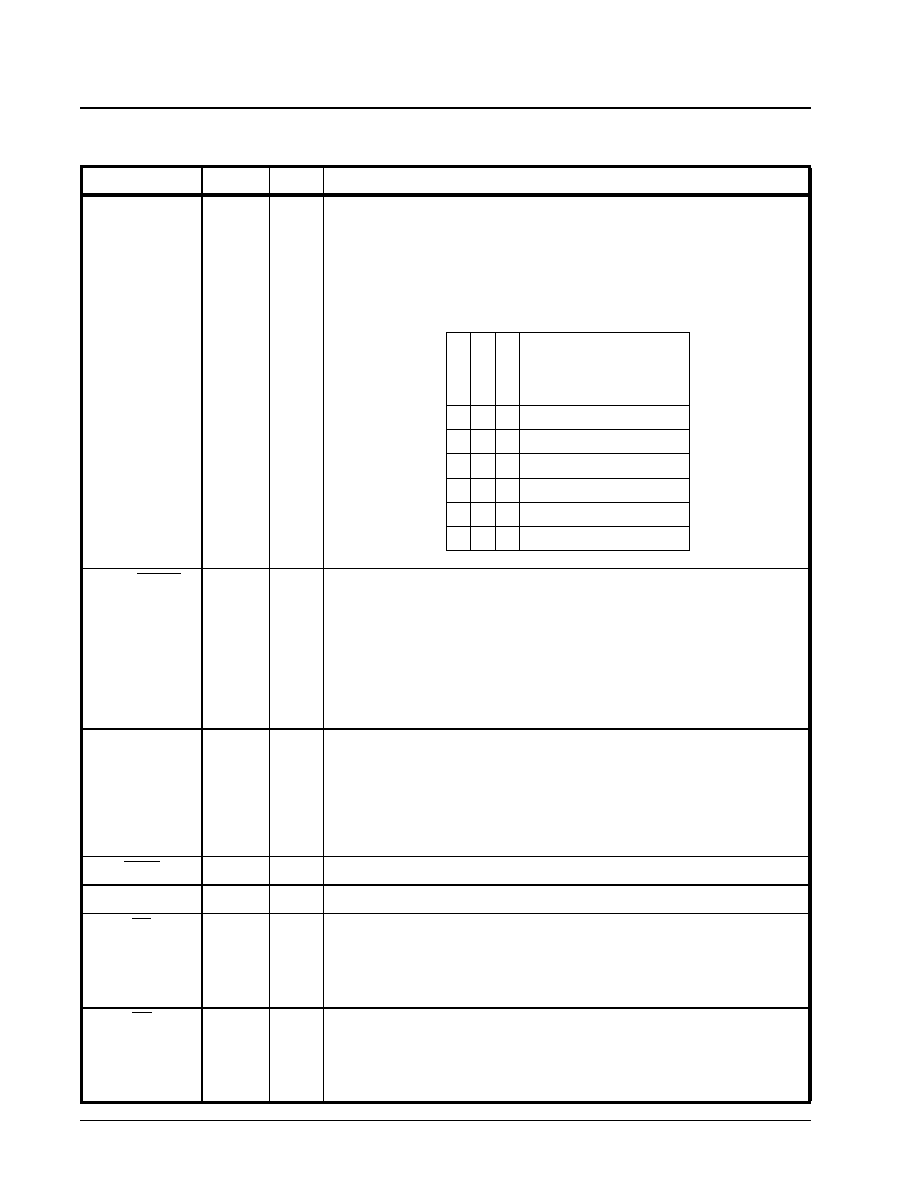
XRT84L38
·Á
·Á
·Á
·Á
OCTAL T1/E1/J1 FRAMER
P1.0.1
PRELIMINARY
31
µ
PType0
µ
PType1
µ
PType2
T25
P24
M25
I
Microprocessor Type Input: Bit 0 (LSB):
This input pin, along with
µ
PTYPE1 and
µ
PTYPE2 permit the user to specify
which type of Microprocessor/Microcontroller to be interfaced the Framer.
Microprocessor Type Input: Bit 1
Microprocessor Type Input: Bit 2
RDY_DTACK
P23
O
Ready/Data Transfer Acknowledge Output:
The exact behavior of this pin depends upon which Microprocessor the Framer
is configured to interface to:
Intel Type Microprocessors
This output pin toggles "Low" when the Framer is ready to respond to the current
PIO (Programmed I/O) or Burst Transaction.
Motorola Type Microprocessors
This output pin toggles "Low" when the Framer has completed the current bus
cycle.
A0
A1
A2
A3
A4
A5
A6
P26
N23
M26
L26
L23
J26
K23
I
Microprocessor Interface Address Bus Input Bit 0 -- (LSB)
Microprocessor Interface Address Bus Input Bit 1
Microprocessor Interface Address Bus Input Bit 2
Microprocessor Interface Address Bus Input Bit 3
Microprocessor Interface Address Bus Input Bit 4
Microprocessor Interface Address Bus Input Bit 5
Microprocessor Interface Address Bus Input Bit 6 -- (MSB)
DBEn
P25
I
Data Bus Enable Input pin.
ALE_AS
N24
I
Address Latch Enable Input_Address Strobe
CS
G25
I
Microprocessor Interface--Chip Select Input:
The Microprocessor/Microcontroller must assert this input pin (toggle it "Low") in
order to exchange data with the Framer.
Note: For the 68K MPU, this signal is generated by address decode and address
strobe.
RD
R26
I
Microprocessor Interface--Read Strobe Input:
The exact behavior of this pin depends upon the type of Microprocessor/Micro-
controller the Framer has been configured to interface to, as defined by the
µ
PTYPE[2:0] pins.
Note: See pin T25 (µPType0) for the µP selection table.
MICROPROCESSOR INTERFACE
(Framer Channel Number indicated by _n)
S
IGNAL
N
AME
P
IN
#
T
YPE
D
ESCRIPTION
0
1
0
1
0
1
µ
µ
µ
µ
PType0
0
0
1
1
0
0
0
0
0
0
1
1
µ
µ
µ
µ
PType1
µ
µ
µ
µ
PType2
68HC11, 8051, 80C188
MOTOROLA 68K
INTEL X86
IDT3051/52
IBM POWER PC 403
INTEL I960
MICROPROCESSOR
TYPE

·Á
·Á
·Á
·Á
XRT84L38
OCTAL T1/E1/J1 FRAMER
PRELIMINARY
REV. P1.0.1
32
WR
G26
I
Microprocessor Interface--Write Strobe Input
"Low" : Indicates current bus cycle is a write cycle: Intel 51, 188, MIPS350x
"High" : Indicates present bus cycle is a write cycle: Intel x86, i960
"Low" : Indicates current bus cycle is a read cycle: Intel x86, i960
"High" : Indicates present bus cycle is a read cycle: Motorola, Power PC 403
"Low" : Also used as write strobe in DMA transfer
ACK0
ACK1
U26
T23
I
I
DMA Cycle Acknowledge Input--DMA Controller 0 (Write):
The external DMA Controller will assert this input pin "High" when the following
two conditions are met:
a. After the DMA Controller, within the Framer has asserted (toggled "Low"), the
Req_0 output signal.
b. When the external DMA Controller is ready to transfer data from external
memory to the selected Transmit HDLC buffer.
At this point, the DMA transfer between the external memory and the selected
Transmit HDLC buffer may begin.
After completion of the DMA cycle, the external DMA Controller will negate this
input pin after the DMA Controller, within the Framer has negated the Req_0
output pin. The external DMA Controller must do this in order to acknowledge
the end of the DMA cycle.
DMA Cycle Acknowledge Input--DMA Controller 1 (Read):
The external DMA Controller asserts this input pin "High" when the following two
conditions are met:
a. After the DMA Controller, within the Framer has asserted (toggled "Low"), the
Req_1 output signal.
b. When the external DMA Controller is ready to transfer data from the selected
Receive HDLC buffer to external memory.
At this point, the DMA transfer between the selected Receive HDLC buffer and
the external memory may begin.
After completion of the DMA cycle, the external DMA Controller will negate this
input pin after the DMA Controller, within the Framer has negated the Req_1
output pin. The external DMA Controller will do this in order to acknowledge the
end of the DMA cycle.
Blast
L25
I
Last Cycle of Burst Indicator Input:
The Microprocessor asserts this pin when it is performing its last read or write
cycle, within a burst operation.
Reset
R3
I
Reset Input: Active "Low"
MICROPROCESSOR INTERFACE
(Framer Channel Number indicated by _n)
S
IGNAL
N
AME
P
IN
#
T
YPE
D
ESCRIPTION

XRT84L38
·Á
·Á
·Á
·Á
OCTAL T1/E1/J1 FRAMER
P1.0.1
PRELIMINARY
33
GROUND PINS
S
IGNAL
N
AME
P
IN
#
T
YPE
D
ESCRIPTION
VDD
L11
L12
L13
L14
L15
L16
M11
M12
M15
M16
N11
N12
N15
N16
R11
R12
R15
R16
****
Power Supply Pins
POWER SUPPLY PINS
S
IGNAL
N
AME
P
IN
#
T
YPE
D
ESCRIPTION
GND
M13
M14
N13
N14
P13
P14
R13
R14
T11
T12
T13
T14
T15
T16
****
Ground Pins

·Á
·Á
·Á
·Á
XRT84L38
OCTAL T1/E1/J1 FRAMER
PRELIMINARY
REV. P1.0.1
34
NO CONNECT PINS
S
IGNAL
N
AME
P
IN
#
T
YPE
D
ESCRIPTION
NC
A6
A20
B7
B17
C12
C13
C16
C23
D14
D17
E1
E2
F4
H25
H26
K26
M23
T24
U3
U4
U25
V3
Y4
AA25
AC23
AD26
AE3
AE14
AE15
AE17
AE25
AF2
AF11
AF14
AF22
AF24
Not Connected

XRT84L38
·Á
·Á
·Á
·Á
OCTAL E1/T1/J1 FRAMER
REV. P1.0.1
PRELIMINARY
35
ELECTRICAL CHARACTERISTICS
ABSOLUTE MAXIMUMS
Power Supply......................................... -0.5V to +3.465V
Power Dissipation PBGA Package........................... 2W
Storage Temperature ...............................-65∞C to 150∞C
Input Logic Signal Voltage (Any Pin) .........-0.5V to + 5.5V
Operating Temperature Range.................-40∞C to 85∞C
ESD Protection...................................................>2000V
Supply Voltage ...................... GND-0.5V to +VDD + 0.5V
Input Current (Any Pin) ...................................... + 100mA
DC ELECTRICAL CHARACTERISTICS
Test Conditions: TA = 25∞C, VDD = 3.3V + 5% unless otherwise specified
S
YMBOL
P
ARAMETER
M
IN
.
T
YP
.
M
AX
.
U
NITS
C
ONDITIONS
I
DD
Power Supply Current
450
mA
All Channels on
I
LL
Data Bus Tri-State Bus Leakage Current
-10
+10
µA
V
IL
Input Low voltage
0.8
V
V
IH
Input High Voltage
2.0
VDD
V
V
OL
Output Low Voltage
0.0
0.4
V
I
OL
= -1.6mA
V
OH
Output High Voltage
2.4
VDD
V
I
OH
= 40µA
I
OC
Open Drain Output Leakage Current
µA
I
IH
Input High Voltage Current
-10
10
µA
V
IH
= VDD
I
IL
Input Low Voltage Current
-10
10
µA
V
IL
= GND

·Á
·Á
·Á
·Á
XRT84L38
OCTAL E1/T1/J1 FRAMER
PRELIMINARY
REV. P1.0.1
36
T
ABLE
2: XRT84L38 P
OWER
C
ONSUMPTION
(Vdd=3.3V±5%, T
A
=25∞C unless otherwise specified)
M
ODE
S
UPPLY
V
OLTAGE
I
MPEDANCE
TERMINATION
R
ESISTOR
T
RANSFORMER
R
ATIO
T
YP
M
AX
U
NIT
T
EST
C
ONDITIONS
R
ECEIVER
T
RANSMITTER
E1
3.3V
75
6.2
2:1
1:2.42
mW
mW
50% "1's"
100% "1's"
E1
3.3V
75
9.1
2:1
1:2
mW
mW
50% "1's"
100% "1's"
E1
3.3V
120
6.2
2:1
1:2.42
mW
mW
50% "1's"
100% "1's"
E1
3.3V
120
9.1
2:1
1:2
mW
mW
50% "1's"
100% "1's"
T1
3.3V
100
3
2:1
1:2.42
mW
mW
50% "1's"
100% "1's"
T1
3.3V
100
3
2:1
1:2
mW
mW
50% "1's"
100% "1's"
---
3.3V
---
---
---
---
mW
All transmitters off

XRT84L38
·Á
·Á
·Á
·Á
OCTAL T1/E1/J1 FRAMER
REV. P1.0.1
PRELIMINARY
37
1.0
MICROPROCESSOR INTERFACE BLOCK
The Microprocessor Interface section supports com-
munication between the local microprocessor (µP)
and the Framer. The Microprocessor Interface sup-
ports the following features:
∑ Communicates through a 6 bit address bus (4 bit for
one framer) and an 8 bit data bus.
∑ Supports DMA read/write data interface
∑ Supports burst transfers
∑ Supports Programmed I/O read and write, wait
cycle extended with READY/DTCK
The Microprocessor Interface section supports the
following operations:
∑ Channel Selection
∑ Writing configuration data into the Framer on-chip
(addressable) registers
∑ Writing outbound PMDL (Path Maintenance Data
Link) messages into the Transmit LAPD Message
buffer of the Framer
∑ Generation of Interrupt Requests to the µP
∑ Servicing Interrupt Requests from the Framer
∑ Monitoring the system's health by periodically read-
ing the on-chip Performance Monitor registers
∑ Reading inbound PMDL Messages from the
Receive LAPD Message Buffer of the Framer
Each of these operations (between the local micro-
processor and the Framer IC) is discussed in detail,
throughout this data sheet.
The Framer supports the following microprocessors/
microcontrollers with a minimum amount of glue logic.
∑ Intel 8051, 80C188, x86, i960
∑ Motorola 68HC11, 68K
∑ MIPS 3051/52
∑ PowerPC 403
The type of microprocessor/microcontroller to inter-
face to the Framer is specified by tying the
µ
P-
TYPE[2:0] pins to the appropriate level. Table 1, lists
the values for
µ
PTYPE[2:0] and the corresponding
µP/µC types.
The behavior of some of the pins, associated with the
Microprocessor Interface, depends upon the value
that the user has applied to the PType[2:0] input pins.
The next sections present a detailed discussion on
the role of each of these pins, and how to configure
the Framer to interface to each of these types of Mi-
croprocessors.
The Framer connects to the Microcontroller as if it
were external memory. The microcontroller can read
or write to two different storage elements in the Fram-
er:
∑ Flip-flop types of registers
∑ RAMs
The configuration of the Framer, including the en-
abling/disabling of interrupts, is selected by setting
values in various control registers. The registers can
be read as well as written. The Framer can be de-
signed into both polled and interrupt-driven systems.
All detection of change of state of alarm conditions,
data link events, error events, or counter overflows
can be programmed to cause interrupts.
The Microcontroller Interface Block within the Framer
supports three types of data transfer schemes:
∑ Programmable Input/Output (PIO)
∑ Burst Transfer
∑ DMA (Direct Memory Access)
Each of these data transfer methods are also dis-
cussed in the next sections.
1.1
C
HANNEL
S
ELECTION
WITHIN
THE
F
RAMER
The XRT84L38 Framer consists of eight independent
banks of configuration registers. Each of these banks
are identical and correspond to each of the eight
channels within the XRT84L38. The XRT84L38 per-
mits selection of and access to, any one of these
Configuration Register Banks, via the Three (3) Most
Significant Address Pins, A4, A5 and A6. The rela-
tionship between the states of A4, A5 and A6, and
T
ABLE
3: µC/µP S
ELECTION
T
ABLE
µ
µ
µ
µ
PTYPE[2:0] I
NPUT
L
EVELS
C
ORRESPONDING
µ
µ
µ
µ
C/
µ
µ
µ
µ
P
000
68HC11, 8051, 80C188
001
Motorola 68000 Family
010
Intel x86 Family
011
Intel I960
100
IDT3051/52 (MIPS)
101
IBM PowerPC 403

·Á
·Á
·Á
·Á
XRT84L38
OCTAL T1/E1/J1 FRAMER
PRELIMINARY
REV. P1.0.1
38
the corresponding "Configuration Register" bank, is
shown below.
1.2
T
HE
M
ICROPROCESSOR
I
NTERFACE
B
LOCK
S
IG
-
NAL
The Framer may be configured into different operat-
ing modes and have its performance monitored by
software through a standard microprocessor, using
data, address and control signals.
The local µP configures the Framer (into a desired
operating mode) by writing data into specific address-
able, on-chip Read/Write registers, or on-chip RAM.
The microprocessor interface provides the signals
which are required for a general purpose micropro-
cessor to read or write data into these registers. The
Microprocessor Interface also supports polled and in-
terrupt driven environments. These interface signals
are described below in Table 5, Table 6, and Table 7.
The microprocessor interface can be configured to
operate in the Motorola Mode, the Intel mode, as well
as other modes. When the Microprocessor Interface
is operating in the Motorola mode, some of the con-
trol signals function in a manner required by the Mo-
torola 68000 family of microprocessors. Likewise,
when the Microprocessor Interface is operating in the
Intel Mode, then these Control Signals function in a
manner as required by the Intel 80xx family of micro-
processors.
Table 5 lists and describes those Microprocessor In-
terface signals whose role is constant across the two
modes. Table 6 describes the role of some of these
signals when the Microprocessor Interface is operat-
ing in the Intel Mode. Likewise, Table 7 describes the
role of these signals when the Microprocessor Inter-
face is operating in the Motorola Mode.
T
ABLE
4: C
HANNEL
S
ELECTION
A6
A5
A4
C
ONFIGURATION
R
EGISTER
B
ANK
0
0
0
Channel 0
0
0
1
Channel 1
0
1
0
Channel 2
0
1
1
Channel 3
1
0
0
Channel 4
1
0
1
Channel 5
1
1
0
Channel 6
1
1
1
Channel 7
F
IGURE
3. S
IMPLIFIED
B
LOCK
D
IAGRAM
OF
THE
M
ICROPROCESSOR
I
NTERFACE
B
LOCK
Microprocessor
Interface
&
Programmable
Registers
DMA
Interface
WR
RD
ALE_AS
Blast
µPType [2:0]
Rdy/Dtack
Reset
DBEn
Clk
CS
INT
A[6:0]
Data[7:0]
ACK[1:0]
Req[1:0]

XRT84L38
·Á
·Á
·Á
·Á
OCTAL T1/E1/J1 FRAMER
REV. P1.0.1
PRELIMINARY
39
T
ABLE
5: XRT84L38 M
ICROPROCESSOR
I
NTERFACE
S
IGNALS
THAT
EXHIBIT
CONSTANT
ROLES
IN
BOTH
THE
I
NTEL
AND
M
OTOROLA
M
ODES
P
IN
N
AME
T
YPE
D
ESCRIPTION
µ
PTYPEe[2:0]
I
Microprocessor Interface Mode Select Input pins
These three pins are used to specify the "Microprocessor Mode" that the Microprocessor Inter-
face will operate in. The relationship between the state of these three input pins, and the corre-
sponding "Microprocessor Mode" is presented in Table 1.
D[7:0]
I/O
Bi-Directional Data Bus for register "Read" or "Write" Operations.
A[6:0]
I
Seven-Bit Address Bus Inputs
The XRT84L38 Framer Microprocessor Interface uses a Multiplexed Address bus. This
address bus is provided to permit the user to select an on-chip register or buffer location for
"Read/Write" access.
CS
I
Chip Select Input
This "active-low" signal selects the Microprocessor Interface of the XRT84L38 Framer and
enables "Read/Write" operations with the on-chip registers/buffer locations.
T
ABLE
6: I
NTEL
MODE
: M
ICROPROCESSOR
I
NTERFACE
S
IGNALS
XRT84L38
P
IN
N
AME
I
NTEL
E
QUIVALENT
P
IN
T
YPE
D
ESCRIPTION
ALE_AS
ALE
I
Address-Latch Enable: This "active-high" signal is used to latch the contents on
the address bus, A[6:0]. The contents of the Address Bus are latched into the
A[6:0] inputs on the falling edge of ALE_AS. Additionally, this signal can be used
to indicate the start of a burst cycle.
RD
RD*
I
Read Signal: This "active-low" input functions as the read signal from the local
µP
. When this signal goes "Low", the UNI Microprocessor Interface will place the
contents of the addressed register on the Data Bus pins (D[7:0]). The Data Bus
will be "tri-stated" once this input signal returns "High".
WR
WR*
I
Write Signal: This "active-low" input functions as the write signal from the local
µP
. The contents of the Data Bus (D[7:0]) will be written into the addressed regis-
ter (via A[6:0]), on the rising edge of this signal.
RDY_DTACK
READY*
O
Ready Output: This "active-low" signal is provided by the UNI device, and indi-
cates that the current read or write cycle is to be extended until this signal is
asserted. The local
µP
will typically insert WAIT states until this signal is
asserted. This output will toggle "Low" when the device is ready for the next Read
or Write cycle.

·Á
·Á
·Á
·Á
XRT84L38
OCTAL T1/E1/J1 FRAMER
PRELIMINARY
REV. P1.0.1
40
1.3
I
NTERFACING
THE
XRT84L38
TO
THE
L
OCAL
µC/
µP
VIA
THE
M
ICROPROCESSOR
I
NTERFACE
B
LOCK
The Microprocessor Interface block within the Framer
is very flexible and provides the following options to
the user.
∑ Interface the Framer to a µC/µP over an 8-bit wide
bi-directional data bus.
∑ Interface the Framer to an Intel-type or Motorola-
type µC/µP.
∑ Transfer data (between the Framer IC and the µC/
µP) via the Programmed I/O or Burst Mode
Each of the options are discussed in detail below.
Section 1.3.1 will discussed the issues associated
with interfacing the Framer to a µC/µP over an 8-bit
bi-directional data bus. Afterwards, Section 1.3.2 will
discuss Data Access (e.g., Programmed I/O and
Burst) Mode when interfaced to both Motorola-type
and Intel-type µC/µP.
1.3.1
Interfacing the Framer to the Micropro-
cessor over an 8 bit wide bi-directional Data Bus
The Framer Microprocessor Interface permits the us-
er to interface it to a µC/µP over an 8-bit wide bi-direc-
tional data bus.
1.3.1.1
Interfacing the Framer to the µC/µP
over an 8-bit wide bi-directional data bus.
In general, interfacing the Framer to an 8-bit µC/µP is
quite straight-forward. This is because most of the
registers, within the Framer, are 8-bits wide. Further,
in this mode, the µC/µP can read or write data into
both even and odd numbered addresses within the
Framer address space.
Reading Performance Monitor (PMON) Registers
A possible complication that the user should be
aware of (while operating in the 8-bit mode) occurs
whenever the µC/µP needs to read the contents of
one of the PMON (Performance Monitor) registers.
The Framer consists of the following PMON Regis-
ters.
∑ T1/E1 receive line code (bipolar) violation counter
∑ T1/E1 receive framing alignment error counter
∑ T1/E1 receive severely errored frame counter
∑ T1/E1 receive CRC-4 block error counter
∑ T1/E1 receive far-end block error counter
∑ T1/E1 receive slip counter
∑ T1/E1 receive loss of frame counter
∑ T1/E1 receive change of frame alignment counter
∑ T1/E1 receive synchronization bit error counter
∑ LAPD frame check sequence error counter
Unlike most of the registers within the Framer, the
PMON registers are 16-bit registers (or 16-bits wide).
Table 82 through Table 94 lists each of these PMON
registers as consisting of two 8-bit registers. One of
these 8-bit register is labeled MSB (or Most Signifi-
cant Byte) and the other register is labeled LSB (or
Least Significant Byte). When an 8-bit PMON Regis-
ter is concatenated with its companion 8-bit PMON
Register, one obtains the full 16-bit expression within
that PMON Register.
The consequence of having these 16-bit registers is
that an 8-bit µC/µP will have to perform two consecu-
tive read operations in order to read in the full 16-bit
expression contained within a given PMON register.
T
ABLE
7: M
OTOROLA
M
ODE
: M
ICROPROCESSOR
I
NTERFACE
S
IGNALS
XRT84L38
P
IN
N
AME
M
OTOROLA
E
QUIVALENT
P
IN
T
YPE
D
ESCRIPTION
ALE_AS
AS*
I
Address Strobe: This "active-low" signal is used to latch the contents on the
address bus input pins: A[6:0] into the Microprocessor Interface circuitry. The
contents of the Address Bus are latched into the UNI device on the rising edge of
the ALE_AS signal. This signal can also be used to indicate the start of a burst
cycle.
RD
DS*
I
Data Strobe: This signal latches the contents of the bi-directional data bus pins
into the Addressed Register (within the UNI) during a Write Cycle.
WR
R/W*
I
Read/Write Input: When this pin is "High", it indicates a Read Cycle. When this
pin is "Low", it indicates a Write cycle.
RDY_DTACK
DTACK*
O
Data Transfer Acknowledge: The Framer asserts DTCK in order to inform the
CPU that the present READ or WRITE cycle is nearly complete. The 68000 fam-
ily of CPUs requires this signal from its peripheral devices, in order to quickly and
properly complete a READ or WRITE cycle.

XRT84L38
·Á
·Á
·Á
·Á
OCTAL T1/E1/J1 FRAMER
REV. P1.0.1
PRELIMINARY
41
In addition, these PMON Registers are Reset-Upon-
Read registers. More specifically, these PMON Reg-
ister are Reset-Upon-Read in the sense that, the en-
tire 16-bit contents, within a given PMON Register is
reset, as soon as an 8-bit µC/µP reads in either byte
of this two-byte (e.g., 16 bit) expression.
Example;
Consider that an 8-bit µC/µP needs to read in the
PMON LCV Event Count Register. In order to accom-
plish this task, the 8-bit µC/µP needs to read in the
contents of PMON LCV Event Count Register - MSB
(located at Address = 0x50) and the contents of the
PMON LCV Event Count Register - LSB (located at
Address = 0x51). These two eight-bit registers, when
concatenated together, make up the PMON LCV
Event Count Register.
If the 8-bit µC/µP reads in the PMON LCV Event
Count-LSB register first, then the entire PMON LCV
Event Count register will be reset to 0x0000. As a
consequence, if the 8-bit µC/µP attempts to read in
the PMON LCV Event Count-MSB register in the very
next read cycle, it will read in the value 0x00.
The PMON Holding Register
In order to resolve this Reset-Upon-Read problem,
the Framer includes a special register, which permits
8-bit µC/µP to read in the full 16-bit contents of these
PMON registers. This special register is called the
PMON Holding Register and is located at 0x6c within
the Framer Address space.
The operation of the PMON Holding register is as fol-
lows. Whenever an 8-bit µC/µP reads in one of the
bytes (of the 2-byte PMON register), the contents of
the unread (e.g., other) byte will be stored in the
PMON Holding Register. Therefore, the 8-bit µC/µP
must then read in the contents of the PMON Holding
Register in the very next read operation.
In Summary: Whenever an 8-bit
µC/µP
needs to
read a PMON Register, it must execute the follow-
ing steps.
Step 1: Read in the contents of a given 8-bit PMON
Register (it does not matter whether the µC/µP reads
in the MSB or the LSB register).
Step 2: Read in the contents of the PMON Holding
Register (located at Address = 0x6c). This register
will contain the contents of the other byte.
1.3.2
Data Access Modes
As mentioned earlier, the Microprocessor Interface
block supports data transfer between the Framer and
the µC/µP (e.g., Read and Write operations) via two
modes: the Programmed I/O and the Burst Modes.
Each of these Data Access Modes are discussed in
detail below.
1.3.2.1
Programmed I/O
Programmed I/O is basically a "handshaking" type of
asynchronous bus access, which provides relatively
slow single read and write data transfers. The Micro-
processor must supply an address value to the
Address Bus input pins A[6:0] with each "read" and
"write" cycle. Because of the "Indirect Addressing"
scheme each PIO reads and write access requires two
accesses, as illustrated below.
In the first access, the Microprocessor is specifying
two things:
1. Which of the four framer register sets it intends to
access.
2. Which group of registers within the "selected"
framer's register sets, the Microprocessor wants
to access.
As a slave, the E1 is the target of access generated
by a bus master, in our case, the CPU. Slave accesses
are accepted by the slave control state machine, then
passed to related functional logic. Address is buffered
and decoded to address relevant destination. Data is
also latch in both write and read directions. PIO oper-
ations are enabled by the Chip Select (CS) input signal.
Framer PIO interface supports pipelined (buffered)
writes to increase bus throughput. All internal registers
and accessible memory are addressable through 6
bits of address bus.
1.3.2.2
Data Access using Programmed I/O
Programmed I/O is the conventional manner in which
a microprocessor exchanges data with a peripheral
device. However, it is also the slowest method of data
exchange between the Framer and the µC/µP.
The next two sections present detailed information on
Programmed I/O Access, when the Framer is operat-
ing in the Intel Mode or in the Motorola Mode.
1.3.2.2.1
Intel Mode Programmed I/O Access
If the Framer is interfaced to an Intel-type µC/µP (e.g.,
the 80x86 family, etc.), then it should be configured to
operate in the Intel mode. Intel-type Read and Write
operations are described below.
1.3.2.2.1.1
Intel Mode Read Cycle
Whenever an Intel-type µC/µP wishes to read the
contents of a register or some location within the Re-
ceive LAPD Message buffer or the Receive OAM Cell
Buffer, (within the Framer), it should do the following.
1. Place the address of the target register or buffer
location (within the Framer) on the Address Bus
input pins A[6:0].
2. While the µC/µP is placing this address value on
the Address Bus, the Address Decoding circuitry
(within the user's system) should assert the CS

·Á
·Á
·Á
·Á
XRT84L38
OCTAL T1/E1/J1 FRAMER
PRELIMINARY
REV. P1.0.1
42
(Chip Select) pin of the Framer, by toggling it
"Low". This action enables further communication
between the µC/µP and the Framer Microproces-
sor Interface block.
3. Toggle the ALE_AS (Address Latch Enable) input
pin "High". This step enables the Address Bus
input drivers, within the Microprocessor Interface
block of the Framer.
4. After allowing the data on the Address Bus pins
to settle (by waiting the appropriate Address Data
Setup time), the µC/µP should toggle the
ALE_AS pin "Low". This step causes the Framer
to latch the contents of the Address Bus into its
internal circuitry. At this point, the address of the
register or buffer locations (within the Framer),
has now been selected.
5. Next, the µC/µP should indicate that this current
bus cycle is a Read Operation by toggling the
RD_DS (Read Strobe) input pin "Low". This
action also enables the bi-directional data bus
output drivers of the Framer. At this point, the bi-
directional data bus output drivers will proceed to
drive the contents of the latched addressed regis-
ter (or buffer location) onto the bi-directional data
bus, D[7:0].
6. Immediately after the µC/µP toggles the Read
Strobe signal "Low", the Framer will toggle the
RDY_DTCK output pin "Low". The Framer does
this in order to inform the µC/µP that the data (to
be read from the data bus) is NOT READY to be
latched into the µC/µP.
7. After some settling time, the data on the bi-direc-
tional data bus will stabilize and can be read by
the µC/µP. The Framer will indicate that this data
can be read by toggling the RDY_DTCK (READY)
signal "High".
8. After the µC/µP detects the RDY_DTCK signal
(from the Framer), it can terminate the Read
Cycle by toggling the RD_DS (Read Strobe) input
pin "High".
Figure 4 presents a timing diagram which illustrates
the behavior of the Microprocessor Interface signals,
during an Intel-type Programmed I/O Read Opera-
tion.
1.3.2.2.1.2
The Intel Mode Write Cycle
Whenever an Intel-type µC/µP wishes to write a byte
or word of data into a register or buffer location, within
the Framer, it should do the following.
1. Assert the ALE_AS (Address Latch Enable) input
pin by toggling it "High". When the µC/µP asserts
the ALE_AS input pin, it enables the Address Bus
Input Drivers within the Framer chip.
2. Place the address of the target register or buffer
location (within the Framer), on the Address Bus
input pins, A[6:0].
3. While the µC/µP is placing this address value
onto the Address Bus, the Address Decoding cir-
cuitry (within the user's system) should assert the
CS input pin of the Framer by toggling it "Low".
This step enables further communication
between the µC/µP and the Framer Microproces-
sor Interface block.
4. After allowing the data on the Address Bus pins
to settle (by waiting the appropriate Address
Setup time), the µC/µP should toggle the
ALE_AS input pin "Low". This step causes the
F
IGURE
4. I
NTEL
µP I
NTERFACE
SIGNALS
DURING
P
ROGRAMMED
I/O R
EAD
O
PERATION
ALE_AS
A[6:0]
CS
D[7:0]
RD
WR
RDY_DTACK
Not Valid
Valid
Address of target Register

XRT84L38
·Á
·Á
·Á
·Á
OCTAL T1/E1/J1 FRAMER
REV. P1.0.1
PRELIMINARY
43
Framer to latch the contents of the Address Bus
into its internal circuitry. At this point, the address
of the register or buffer location (within the
Framer), has now been selected.
5. Next, the µC/µP should indicate that this current
bus cycle is a Write Operation by toggling the
WR_R/W
(Write Strobe) input pin "Low". This
action also enables the bi-directional data bus
input drivers of the Framer.
6. The µC/µP should then place the byte or word
that it intends to write into the target register, on
the bi-directional data bus, D[7:0].
7. After waiting the appropriate amount of time for
the data (on the bi-directional data bus) to settle,
the µC/µP should toggle the
WR_R/W
(Write
Strobe) input pin "High". This action accom-
plishes two things:
a. It latches the contents of the bi-directional data
bus into the Framer Microprocessor Interface
block.
b. It terminates the write cycle.
Figure 5 presents a timing diagram which illustrates
the behavior of the Microprocessor Interface signals,
during an Intel-type Programmed I/O Write Opera-
tion.
1.3.2.2.2
Motorola Mode Programmed I/O
Access
If the Framer is interfaced to a Motorola-type µC/µP
(e.g., the MC680X0 family, etc.), it should be config-
ured to operate in the Motorola mode. Motorola-type
Programmed I/O Read and Write operations are de-
scribed below.
1.3.2.2.2.1
Motorola Mode Read Cycle
Whenever a Motorola-type µC/µP wishes to read the
contents of a register or some location within the Re-
ceive LAPD Message or Receive OAM Cell Buffer,
(within the Framer) it should do the following.
1. Assert the ALE_AS (Address-Strobe) input pin by
toggling it low. This step enables the Address Bus
input drivers, within the Microprocessor Interface
Block of the Framer.
2. Place the address of the target register (or buffer
location) within the Framer, on the Address Bus
input pins, A[6:0].
3. At the same time, the Address Decoding circuitry
(within the user's system) should assert the CS
(Chip Select) input pin of the Framer, by toggling
it "Low". This action enables further communica-
tion between the µC/µP and the Framer Micropro-
cessor Interface block.
4. After allowing the data on the Address Bus pins
to settle (by waiting the appropriate Address
Setup time), the µC/µP should toggle the
ALE_AS input pin "High". This step causes the
Framer to latch the contents of the Address Bus
into its internal circuitry. At this point, the address
of the register or buffer location (within the
Framer) has been selected.
5. Further, the µC/µP should indicate that this cycle
is a Read cycle by setting the
WR_R/W
(R/W*)
input pin "High".
6. Next the µC/µP should initiate the current bus
cycle by toggling the RD_DS (Data Strobe) input
pin "Low". This step enables the bi-directional
data bus output drivers, within the Framer. At this
F
IGURE
5. I
NTEL
µP I
NTERFACE
S
IGNALS
,
DURING
P
ROGRAMMED
I/O W
RITE
O
PERATION
ALE_AS
A[6:0]
CS
D[7:0]
RD
WR
RDY_DTACK
Data to be Written
Address of Target Register

·Á
·Á
·Á
·Á
XRT84L38
OCTAL T1/E1/J1 FRAMER
PRELIMINARY
REV. P1.0.1
44
point, the bi-directional data bus output drivers
will proceed to drive the contents of the Address
register onto the bi-directional data bus, D[7:0].
7. After some settling time, the data on the bi-direc-
tional data bus will stabilize and can be read by
the µC/µP. The Framer will indicate that this data
can be read by asserting the RDY_DTCK
(DTACK) signal "Low".
8. After the µC/µP detects the RDY_DTCK signal
(from the Framer) it will terminate the Read Cycle
by toggling the RD_DS (Data Strobe) input pin
"High".
Figure 6 presents a timing diagram which illustrates
the behavior of the Microprocessor Interface signals
during a Motorola-type Programmed I/O Read Opera-
tion.
1.3.2.2.2.2
Motorola Mode Write Cycle
Whenever a Motorola-type µC/µP wishes to write a
byte or word of data into a register or buffer location,
within the Framer, it should do the following.
1. Assert the ALE_AS (Address Select) input pin by
toggling it "Low". This step enables the Address
Bus input drivers (within the Framer chip).
2. Place the address of the target register or buffer
location (within the Framer), on the Address Bus
input pins, A[6:0].
3. While the µC/µP is placing this address value
onto the Address Bus, the Address-Decoding cir-
cuitry (within the user's system) should assert the
CS (Chip Select) input pins of the Framer by tog-
gling it "Low". This step enables further communi-
cation between the µC/µP and the Framer Micro-
processor Interface block.
4. After allowing the data on the Address Bus pins
to settle (by waiting the appropriate Address
Setup time), the µC/µP should toggle the
ALE_AS input pin "High". This step causes the
Framer to latch the contents of the Address Bus
into its own circuitry. At this point, the Address of
the register or buffer location (within the Framer),
has now been selected.
5. Further, the µC/µP should indicate that this cur-
rent bus cycle is a Write operation by toggling the
WR_R/W
(R/W*) input pin "Low".
6. The µC/µP should then place the byte or word
that it intends to write into the target register, on
the bi-directional data bus, D[7:0].
7. Next, the µC/µP should initiate the bus cycle by
toggling the RD_DS (Data Strobe) input pin
"Low". When the Framer senses that the
WR_R/W
(R/W*) input pin is "High" and that the RD_DS
(Data Strobe) input pin has toggled "Low", it will
enable the input drivers of the bi-directional data
bus, D[7:0].
8. After waiting the appropriate time, for this newly
placed data to settle on the bi-directional data
bus (e.g., the Data Setup time) the Framer will
assert the RDY_DTCK output signal "Low".
9. After the µC/µP detects the RDY_DTCK signal
(from the Framer), the µC/µP should toggle the
RD_DS input pin "High". This action accom-
plishes two things.
F
IGURE
6. M
OTOROLA
µP I
NTERFACE
SIGNALS
,
DURING
A
P
ROGRAMMED
I/O R
EAD
O
PERATION
ALE_AS
A[6:0]
CS
D[7:0]
RD_DS
WR_R/W
RDY_DTACK
Not Valid
Address of target Register
Valid Data

XRT84L38
·Á
·Á
·Á
·Á
OCTAL T1/E1/J1 FRAMER
REV. P1.0.1
PRELIMINARY
45
a.
It latches the contents of the bi-directional data bus
into the Microprocessor Interface block.
b.
It terminates the Write cycle.
Figure 7 presents a timing diagram which illustrates
the behavior of the Microprocessor Interface signals,
during a Motorola-type Programmed I/O Write Opera-
tion.
1.3.2.3
Burst Mode I/O for Data Access
Burst Mode I/O access is a much faster way to trans-
fer data between the µC/µP and the Microprocessor
Interface (of the Framer), than Programmed I/O. The
reason why Burst Mode I/O is faster is explained be-
low.
Data is placed upon the Address Bus input pins
A[6:0] only for the very first access, within a given
burst access. The remaining read or write operations
(within this burst access) do not require the place-
ment of the Address Data on the Address Data Bus.
As a consequence, the user does not have to wait
through the Address Setup and Hold times for each of
these Read/Write operation, within the Burst Access.
It is important to note that there are some limitations
associated with Burst Mode I/O Operations.
1. All cycles within the Burst Access, must be either
all Read or all Write cycles. No mixing of Read
and Write cycles is permitted.
2. A Burst Access can only be used when Read or
Write operations are to be employed over a con-
tiguous range of address locations, within the
Framer.
3. The very first Read or Write cycle, within a burst
access, must start at the lowest address value, of
the range of addresses to be accessed. Subse-
quent operations will automatically be incre-
mented to the very next higher address value.
Examples of Burst Mode I/O operations are present-
ed below for read and write operations, with both In-
tel-type and Motorola-type µC/µP.
1.3.2.3.1
Burst I/O Access: Intel Mode
If the XRT84L38 Framer is interfaced to an Intel-type
µC/µP (e.g., the 80x86 family, etc.), then it should be
configured to operate in the Intel mode (by tying the
MOTO pin to ground). Intel-type Read and Write
Burst I/O Access operations are described below.
1.3.2.3.1.1
Intel-Mode Read Burst Access
When an Intel-type µC/µP wants to read the contents
of numerous registers or buffer locations over a con-
tiguous range of addresses, then it should do the fol-
lowing.
a. Perform the initial read operation of the burst
access.
b. Perform the remaining read operations of the
burst access.
c. Terminate the burst access operation.
Each of these operations within the burst access are
described below.
1.3.2.3.1.1.1
Initial Read Operation: Intel mode
The initial read operation of an Intel-type read burst
access is accomplished by executing a Programmed
I/O Read Cycle as summarized below.
F
IGURE
7. M
OTOROLA
µP I
NTERFACE
SIGNAL
DURING
P
ROGRAMMED
I/O W
RITE
O
PERATION
ALE_AS
A[6:0]
CS
D[7:0]
RD
WR
RDY_DTACK
Data to be Written
Address of target Register

·Á
·Á
·Á
·Á
XRT84L38
OCTAL T1/E1/J1 FRAMER
PRELIMINARY
REV. P1.0.1
46
A.0
Execute a Single Ordinary (Programmed I/O)
Read Cycle, as described in steps A.1 through
A.7 below.
A.1
Place the address of the initial-target register or
buffer location (within the Framer) on the
Address Bus input pins A[6:0].
A.2
While the µC/µP is placing this address value
onto the Address Bus, the Address Decoding
circuitry (within the user's system) should
assert the CS input pin of the Framer, by tog-
gling it "Low". This step enables further com-
munication between the µC/µP and the Framer
Microprocessor Interface block.
A.3
Assert the ALE_AS (Address Latch Enable) pin
by toggling it "High". This step enables the
Address Bus input drivers, within the Micropro-
cessor Interface block of the Framer.
A.4
After allowing the data on the Address Bus pins
to settle (by waiting the appropriate Address
Data Setup time), the µC/µP should then toggle
the ALE_AS pin "Low". This step latches the
contents, on the Address Bus pins, A[6:0], into
the Framer Microprocessor Interface block. At
this point, the initial address of the burst access
has now been selected.
N
OTE
: The ALE_AS input pin should remain "Low" for the
remainder of this Burst Access operation.
A.5
Next, the µC/µP should indicate that this cur-
rent bus cycle is a Read Operation by toggling
the RD_DS (Read Strobe) input pin "Low". This
action also enables the bi-directional data bus
output drivers of the Framer. At this point, the
bi-directional data bus output drivers will pro-
ceed to drive the contents of the addressed
register onto the bi-directional data bus, D[7:0].
A.6
Immediately after the µC/µP toggles the Read
Strobe signal "Low", the Framer will toggle the
RDY_DTCK (READY) output pin "Low". The
Framer does this in order to inform the µC/µP
that the data (to be read from the data bus) is
NOT READY to be latched into the µC/µP.
A.7
After some settling time, the data on the bi-
directional data bus will stabilize and can be
read by the µC/µP. The Framer will indicate that
this data is ready to be read, by toggling the
RDY_DTCK (Ready) signal "High".
A.8
After the µC/µP detects the RDY_DTCK signal
(from the Framer), it can then will terminate the
Read cycle by toggling the RD_DS (Read
Strobe) input pin "High".
Figure 8 presents an illustration of the behavior of the
Microprocessor Interface Signals, during the initial
Read Operation, within a Burst I/O Cycle for an Intel-
type µC/µP.
At the completion of this initial read cycle, the µC/µP
has read in the contents of the first register or buffer
location (within the Framer) for this particular burst I/
O access operation. In order to illustrate how this
burst access operation works, the byte (or word) of
data, that is being read in Figure 8, has been labeled
Valid Data at Offset = 0x00. This label indicates that
the µC/µP is reading the very first register (or buffer
location) in this burst access operation.
F
IGURE
8. I
NTEL
µP I
NTERFACE
S
IGNALS
,
DURING
THE
I
NITIAL
R
EAD
O
PERATION
OF
A
B
URST
C
YCLE
RDY_DTACK
ALE_AS
A[6:0]
CS
D[7:0]
RD
WR
Not Valid
Address of "Initial" Target Register (Offset = 0x00)
Valid Data of
Offset = 0x00

XRT84L38
·Á
·Á
·Á
·Á
OCTAL T1/E1/J1 FRAMER
REV. P1.0.1
PRELIMINARY
47
1.3.2.3.1.1.2
Subsequent Read Operations
The procedure that the µC/µP must use to perform
the remaining read cycles, within this Burst Access
operation, is presented below.
B.0
Execute each subsequent Read Cycles, as
described in steps 1 through 3 below.
B.1
Without toggling the ALE_AS input pin (e.g.,
keeping it "Low"), toggle the RD_DS input pin
"Low". This step accomplishes the following.
a.
The Framer will internally increments the latched
address value (within the Microprocessor Interface
circuitry).
b.
The output drivers of the bi-directional data bus,
D[7:0] are enabled. At some time later, the register
or buffer location corresponding to the incremented
latched address value will be driven onto the bi-
directional data bus.
B.2
Immediately after the Read Strobe pin toggles
"Low" the Framer will toggle the RDY_DTCK
(READY) output pin "Low" to indicate its NOT
READY status.
B.3
After some settling time, the data on the bi-
directional data bus will stabilize and can be
read by the µC/µP. The Framer will indicate that
this data is ready to be read by toggling the
RDY_DTCK (READY) signal "High".
B.4
After the µC/µP detects the RDY_DTCK signal
(from the Framer), it can terminate the Read
cycle by toggling the RD_DS (Read Strobe)
input pin "High".
For subsequent read operations, within this burst cy-
cle, the µC/µP simply repeats steps 1 through 3, as il-
lustrated in Figure 9.
In addition to the behavior of the Microprocessor In-
terface signals, Figure 9 also illustrates other points
regarding the Burst Access Operation.
a. The Framer internally increments the address
value, from the original latched value shown in
Figure 8. This is illustrated by the data, appearing
on the data bus, (for the first read access) being
labeled Valid Data at Offset = 0x01 and that for
the second read access being labeled Valid Data
at Offset = 0x02.
b. The Framer performs this address incrementing
process even though there are no changes in the
Address Bus Data, A[6:0].
1.3.2.3.1.1.3
Terminating the Burst Access
Operation
The Burst Access Operation will be terminated upon
the rising edge of the ALE_AS input signal. At this
point the Framer will cease to internally increment the
latched address value. Further, the µC/µP is now free
to execute either a Programmed I/O access or to start
another Burst Access Operation with the Framer.
1.3.2.3.1.2
Write Burst Access: Intel-Mode
When an Intel-type µC/µP wishes to write data into a
contiguous range of addresses, then it should do the
following.
a. Perform the initial write operation of the burst
access.
b. Perform the remaining write operations, of the
burst access.
F
IGURE
9. I
NTEL
µP I
NTERFACE
S
IGNALS
,
DURING
SUBSEQUENT
R
EAD
O
PERATIONS
OF
A
B
URST
I/O C
YCLE
RDY_DTACK
ALE_AS
A[6:0]
CS
D[7:0]
RD
WR
Not
Valid
Address of "Initial" Target Register (Offset = 0x00)
Valid Data at
Offset = 0x01
Not
Valid
Valid Data at
Offset = 0x02

·Á
·Á
·Á
·Á
XRT84L38
OCTAL T1/E1/J1 FRAMER
PRELIMINARY
REV. P1.0.1
48
c. Terminate the burst access operation.
Each of these operations within the burst access are
described below.
1.3.2.3.1.2.1
Initial Write Operation
The initial write operation of an Intel-type Write Burst
Access is accomplished by executing a Programmed
I/O write cycle as summarized below.
A.0
Execute a Single Ordinary (Programmed I/O)
Write cycle, as described in Steps A.1 through
A.7 below.
A.1
Place the address of the initial target register
(or buffer location) within the Framer, on the
Address Bus pins, A[6:0].
A.2
At the same time, the Address-Decoding cir-
cuitry (within the user's system) should assert
the CS (Chip Select) input pin of the Framer, by
toggling it "Low". This step enables further
communication between the µC/µP and the
Framer Microprocessor Interface block.
A.3
Assert the ALE_AS (Address Latch Enable)
input pin "High". This step enables the Address
Bus input drivers, within the Microprocessor
Interface Block of the Framer.
A.4
After allowing the data on the Address Bus pins
to settle (by waiting the appropriate Address
Setup time), the µC/µP should then toggle the
ALE_AS input pin "Low". This step latches the
contents, on the Address Bus pins, A[6:0], into
the XRT84L38 Framer Microprocessor Inter-
face block. At this point, the initial address of
the burst access has now been selected.
N
OTE
: The ALE_AS input pin should remain "Low" for the
remainder of this Burst I/O Access operation.
A.5
Next, the µC/µP should indicate that this cur-
rent bus cycle is a Write operation by keeping
the RD_DS pin "High" and toggling the
WR_R/
W
(Write Strobe) pin "Low". This action also
enables the bi-directional data bus input drivers
of the Framer.
A.6
The µC/µP places the byte (or word) that it
intends to write into the target register on the
bi-directional data bus, D[7:0].
A.7
After waiting the appropriate amount of time, for
the data (on the bi-directional data bus) to set-
tle, the µC/µP should toggle the
WR_R/W
(Write
Strobe) input pin "High". This action accom-
plishes two things.
a. It latches the contents of the bi-directional data
bus into the Framer Microprocessor Interface
Block.
b. It terminates the write cycle.
Figure 10 presents a timing diagram which illustrates
the behavior of the Microprocessor Interface signals,
during the initial write operation within a Burst Ac-
cess, for an Intel-type µC/µP.
At the completion of this initial write cycle, the µC/µP
has written a byte or word into the first register or
buffer location (within the Framer) for this particular
burst access operation. In order to illustrate this point,
the byte (or word) of data, that is being written in
Figure 10 has been labeled Data to be Written (Offset
= 0x00).
F
IGURE
10. I
NTEL
µP I
NTERFACE
SIGNALS
,
DURING
THE
I
NITIAL
W
RITE
O
PERATION
OF
A
B
URST
C
YCLE
RDY_DTACK
ALE_AS
A[6:0]
CS
D[7:0]
RD
WR
Address of "Initial" Target Register (Offset = 0x00)
Data to be Written
(Offset = 0x00)

XRT84L38
·Á
·Á
·Á
·Á
OCTAL T1/E1/J1 FRAMER
REV. P1.0.1
PRELIMINARY
49
1.3.2.3.1.2.2
The Subsequent Write Operations
The procedure that the µC/µP must use to perform
the remaining write cycles, within this burst access
operation, is presented below.
B.0
Execute each subsequent write cycle, as
described in steps B.1 through B.3.
B.1
Without toggling the ALE_AS input pin (e.g.,
keeping it "Low"), apply the value of the next
byte or word (to be written into the Framer) to
the bi-directional data bus pins, D[7:0].
B.2
Toggle the
WR_R/W
(Write Strobe) input pin
"Low". This step accomplishes two things.
a. It enables the input drivers of the bi-directional
data bus.
b. It causes the Framer to internally increment the
value of the latched address.
B.3
After waiting the appropriate amount of settling
time the data, in the internal data bus, will stabi-
lize and is ready to be latched into the Framer
Microprocessor Interface block. At this point,
the µC/µP should latch the data into the Framer
by toggling the
WR_R/W
input pin "High".
For subsequent write operations, within this burst I/O
access, the µC/µP simply repeats steps B.1 through
B.3, as illustrated in Figure 11.
1.3.2.3.1.2.3
Terminating the Burst I/O Access
Burst Access Operation will be terminated upon the
rising edge of the ALE_AS input signal. At this point
the Framer will cease to internally increment the
latched address value. Further, the µC/µP is now free
to execute either a Programmed I/O access or to start
another Burst Access Operation with the XRT84L38
Framer.
1.3.2.3.2
Burst I/O Access: Motorola Mode
If the XRT84L38 Framer is interfaced to a Motorola-
type µC/µP (e.g., the MC680x0 family, etc.), then it
should be configured to operate in the Motorola mode
(by tying the MOTO pin to VCC). Motorola-type Read
and Write Burst I/O Access operations are described
below.
1.3.2.3.2.1
Read Burst I/O Access Operation:
Motorola-Mode
Whenever a Motorola-type µC/µP wishes to read the
contents of numerous registers or buffer locations
over a contiguous range of addresses, then it should
do the following.
a. Perform the initial Read operation of the burst
access.
b. Perform the remaining read operations in the
burst access.
c. Terminate the burst access operation.
Each of these operations, within the Burst Access are
discussed below.
1.3.2.3.2.1.1
Initial Read Operation: Motorola
Mode
The initial read operation of a Motorola-type read
burst access is accomplished by executing a Pro-
grammed I/O Read cycle, as summarized below.
A.0
Execute a Single Ordinary (Programmed I/O)
Read Cycle, as described in steps A.1 through
A.8 below.
F
IGURE
11. µP I
NTERFACE
S
IGNALS
,
DURING
SUBSEQUENT
W
RITE
O
PERATIONS
OF
A
B
URST
I/O C
YCLE
RDY_DTACK
ALE_AS
A[6:0]
CS
D[7:0]
RD
WR
Address of "Initial" Target Register (Offset = 0x00)
Data Written at Offset = 0x01
Data Written at Offset = 0x02

·Á
·Á
·Á
·Á
XRT84L38
OCTAL T1/E1/J1 FRAMER
PRELIMINARY
REV. P1.0.1
50
A.1
Assert the ALE_AS (AS) input pin by toggling it
"Low". This step enables the Address Bus input
drivers (within the Framer) within the Framer
Microprocessor Interface Block.
A.2
Place the address of the initial target register or
buffer location (within the Framer), on the
Address Bus input pins, A[6:0].
A.3
At the same time, the Address-Decoding cir-
cuitry (within the user's system) should assert
the CS (Chip Select) input pins of the Framer
by toggling it "Low". This action enables further
communication between the µC/µP and the
Framer Microprocessor Interface block.
A.4
After allowing the data on the Address Bus pins
to settle (by waiting the appropriate Address
Setup time), the µC/µP should toggle the
ALE_AS input pin "High". This step causes the
Framer to latch the contents of the Address Bus
into its internal circuitry. At this point, the initial
address of the burst access has now been
selected.
A.5
Further, the µC/µP should indicate that this
cycle is a Read cycle by setting the
WR_R/W
(R/W) input pin "High".
A.6
Next the µC/µP should initiate the current bus
cycle by toggling the RD_DS (Data Strobe)
input pin "Low". This step will enable the bi-
directional data bus output drivers, within the
Framer. At this point, the bi-directional data bus
output drivers will proceed to driver the con-
tents of the Address register onto the bi-direc-
tional data bus.
A.7
After some settling time, the data on the bi-
directional data bus will stabilize and can be
read by the µC/µP. The Framer will indicate that
this data can be read by asserting the
RDY_DTCK (DTACK) signal "Low".
A.8
After the µC/µP detects the RDY_DTCK signal
(from the Framer) it will terminate the Read
Cycle by toggling the RD_DS (Data Strobe)
input pin "High".
Figure 12 presents an illustration of the behavior of
the Microprocessor Interface Signals during the initial
Read Operation, within a Burst I/O Cycle, for a Motor-
ola-type µC/µP.
At the completion of this initial read cycle, the µC/µP
has read in the contents of the first register or buffer
location (within the Framer) for this particular burst
access operation. In order to illustrate how this burst
I/O cycle works, the byte (or word) of data, that is be-
ing read in Figure 12 has been labeled Valid Data at
Offset = 0x00. This indicates that the µC/µP is read-
ing the very first register (or buffer location) in this
burst access.
1.3.2.3.2.1.2
Subsequent Read Operations
The procedure that the µC/µP must use to perform
the remaining read cycles, within this Burst Access
operation, is presented below.
B.0
Execute each subsequent Read Cycle, as
described in steps B.1 through B.3, below.
B.1
Without toggling the ALE_AS input pin (e.g.,
keeping it "High"), toggle the RD_DS (Data
F
IGURE
12. M
OTOROLA
µP I
NTERFACE
S
IGNALS
,
DURING
THE
I
NITIAL
R
EAD
O
PERATION
OF
A
B
URST
C
YCLE
ALE_AS
A[6:0]
CS
D[7:0]
RD
WR
RDY_DTACK
Not Valid
Address of "Initial" Target Register (Offset = 0x00)
Valid Data at
Offset = 0x00

XRT84L38
·Á
·Á
·Á
·Á
OCTAL T1/E1/J1 FRAMER
REV. P1.0.1
PRELIMINARY
51
Strobe) input pin "Low". This step accom-
plishes the following.
a. The Framer internally increments the latched
address value (within the Microprocessor Inter-
face circuitry).
b. The output drivers of the bi-directional data bus
(D[7:0]) are enabled. At some time later, the reg-
ister or buffer location corresponding to the incre-
mented latched address value will be driven onto
the bi-directional data bus.
N
OTE
: In order to insure that the Framer will interpret this
signal as being a Read signal, the
µC/µP
should keep the
WR_R/W input pin "High".
B.2
After some settling time, the data on the bi-
directional data bus will stabilize and can be
read by the µC/µP. The Framer will indicate that
this data is ready to be read by asserting the
RDY_DTCK (DTACK) signal "Low".
B.3
After the µC/µP detects the RDY_DTCK signal
(from the Framer), it terminates the Read cycle
by toggling the RD_DS (Data Strobe) input pin
"High".
For subsequent read operations, within this burst cy-
cle, the µC/µP simply repeats steps B.1 through B.3,
as illustrated in Figure 13.
1.3.2.3.2.1.3
Terminating Burst Access Opera-
tion
The Burst I/O Access will be terminated upon the fall-
ing edge of the ALE_AS input signal. At this point the
Framer will cease to internally increment the latched
address value. Further, the µC/µP is now free to exe-
cute either a Programmed I/O access or to start an-
other Burst Access Operation with the Framer.
1.3.2.3.2.2
Write Burst Access: Motorola-Mode
Whenever a Motorola-type µC/µP wishes to write the
contents of numerous registers or buffer locations
over a contiguous range of addresses, then it should
do the following.
a. Perform the initial write operation of the burst
access.
b. Perform the remaining write operations, of the
burst access.
c. Terminate the burst access operation.
Each of these operations within the burst access are
described below.
1.3.2.3.2.2.1
Initial Write Operation
The initial write operation of a Motorola-type Write
Burst Access is accomplished by executing a Pro-
grammed I/O Write Cycle as summarized below.
A.0
Execute a Single Ordinary (Programmed I/O)
Write cycle, as described in Steps A.1 through
A.7 below.
A.1
Assert the ALE_AS (Address Strobe) input pin
by toggling it "Low". This step enables the
Address Bus input drivers (within the Framer).
A.2
Place the address of the initial target register or
buffer location (within the Framer), on the
Address Bus input pins, A[6:0].
A.3
At the same time, the Address-Decoding cir-
cuitry (within the user's system) should assert
the CS input pin of the Framer by toggling it
"Low". This step enables further communica-
F
IGURE
13. M
OTOROLA
µP I
NTERFACE
S
IGNALS
,
DURING
SUBSEQUENT
R
EAD
O
PERATIONS
OF
A
B
URST
I/O C
YCLE
RDY_DTACK
ALE_AS
A[6:0]
CS
D[7:0]
RD
WR
Not Valid
Address of "Initial" Target Register (Offset = 0x00)
Valid Data at
Offset = 0x01
Not Valid
Valid Data at
Offset = 0x02

·Á
·Á
·Á
·Á
XRT84L38
OCTAL T1/E1/J1 FRAMER
PRELIMINARY
REV. P1.0.1
52
tion between the µC/µP and the Framer Micro-
processor Interface block.
A.4
After allowing the data on the Address Bus pins
to settle (by waiting the appropriate Address
Setup time), the µC/µP should toggle the
ALE_AS input pin "High". This step causes the
Framer to latch the contents of the Address Bus
into its own circuitry. At this point, the initial
address of the burst access has now been
selected.
A.5
Further, the µC/µP should indicate that this cur-
rent bus cycle is a Write operation by toggling
the
WR_R/W
(R/W) input pin "Low".
A.6
The µC/µP should then place the byte or word
that it intends to write into the target register, on
the bi-directional data bus, D[7:0].
A.7
Next, the µC/µP should initiate the bus cycle by
toggling the RD_DS (Data Strobe) input pin
"Low". When the XRT84L38 Framer senses
that the
WR_R/W
input pin is "Low", and that the
RD_DS input pin has toggled "Low" it will
enable the input drivers of the bi-directional
data bus, D[7:0].
A.8
After waiting the appropriate amount of time, for
this newly placed data to settle on the bi-direc-
tional data bus (e.g., the Data Setup time) the
Framer will assert the RDY_DTCK (DTACK)
output signal.
A.9
After the µP/µC detects the RDY_DTCK signal
(from the Framer) it should toggle the RD_DS
input pin "High". This action accomplishes two
things:
a.
It latches the contents of the bi-directional data bus
into the Framer Microprocessor Interface block.
b.
It terminates the Write cycle.
Figure 14 presents a timing diagram which illustrates
the behavior of the Microprocessor Interface signals,
during the Initial write operation within a Burst Ac-
cess, for a Motorola-type µC/µP.
At the completion of this initial write cycle, the µC/µP
has written a byte or word into the first register or
buffer location (within the Framer) for this particular
burst I/O access. In order to illustrate how this burst I/
O cycle works, the byte (or word) of data, that is being
written in Figure 14 has been labeled Data to be Writ-
ten (Offset = 0x00).
1.3.2.3.2.2.2
The Subsequent Write Operations
The procedure that the µC/µP must use to perform
the remaining write cycles, within this burst access
operation, is presented below.
B.0
Execute each subsequent write cycle, as
described in steps B.1 through B.3.
B.1
Without toggling the ALE_AS input pin (e.g.,
keeping it "Low"), apply the value of the next
byte or word (to be written into the Framer) to
the bi-directional data bus pins, D[7:0].
B.2
Toggle the
WR_R/W
(Write Strobe) input pin
"Low". This step accomplishes two things.
a. It enables the input drivers of the bi-directional
data bus.
F
IGURE
14. M
OTOROLA
µP I
NTERFACE
SIGNALS
,
DURING
THE
I
NITIAL
W
RITE
O
PERATION
OF
A
B
URST
C
YCLE
RDY_DTACK
ALE_AS
A[6:0]
CS
D[7:0]
RD
WR
Data to be Written
(Offset = 0x00)
Address of "Initial" Target Register (Offset = 0x00)

XRT84L38
·Á
·Á
·Á
·Á
OCTAL T1/E1/J1 FRAMER
REV. P1.0.1
PRELIMINARY
53
b. It causes the Framer to internally increment the
value of the latched address.
B.3
After waiting the appropriate amount of settling
time the data, in the internal data bus, will stabi-
lize and is ready to be latched into the Framer
Microprocessor Interface block. At this point,
the µC/µP should latch the data into the Framer
by toggling the
WR_R/W
input pin "High".
For subsequent write operations, within this burst I/O
access, the µC/µP simply repeats steps B.1 through
B.3, as illustrated in Figure 15.
1.3.2.3.2.2.3
Terminating the Burst I/O Access
The Burst I/O Access will be terminated upon the fall-
ing edge of the ALE_AS input signal. At this point the
Framer will cease to internally increment the latched
address value. Further, the µC/µP is now free to exe-
cute either a Programmed I/O access or to start an-
other Burst I/O Access with the Framer.
1.4
DMA R
EAD
/W
RITE
O
PERATIONS
The XRT84L38 Framer contains two DMA Controller
Interfaces which provide support for all eight framers
within the chip. The purpose of the two DMA Control-
lers is to facilitate the rapid block transfer of data be-
tween an external memory location and the on-chip
HDLC buffers via the Microprocessor Interface.
DMA-0 W
RITE
DMA I
NTERFACE
DMA 0 Controller Interface handles data transfer be-
tween external memory and the "selected" Transmit
HDLC Buffer.
The DMA cycle starts when the XRT84L38 asserts
the REQ0 output pin. The "external" DMA Controller
then responds by asserting the ACK0 input pin. The
contents of the Microprocessor Interface bi-direction-
al data bus are latched into the XRT84L38 each time
the pWRL (Write Strobe) input pin is strobed "low".
The XRT84L38 ends the DMA cycle by negating the
DMA request input (REQ0) while WR is still active.
The external DMA Controller acknowledges the end of
DMA Transfer by driving the ACK0 input pin "high".
F
IGURE
15. M
OTOROLA
µP I
NTERFACE
S
IGNALS
,
DURING
SUBSEQUENT
W
RITE
O
PERATIONS
OF
A
B
URST
I/O
C
YCLE
RDY_DTACK
ALE_AS
A[6:0]
CS
D[7:0]
RD
WR
Address of "Initial" Target Register (Offset = 0x00)
Data Written at Offset = 0x01
Data Written at Offset = 0x02

·Á
·Á
·Á
·Á
XRT84L38
OCTAL T1/E1/J1 FRAMER
PRELIMINARY
REV. P1.0.1
54
1.5
M
EMORY
AND
R
EGISTER
M
AP
This section presents a complete list of the Framer
external memory address map and the internal mem-
ory map. In addition, the allocations of the three inter-
nal storage spaces is depicted.
1.5.1
Memory Mapped I/O Indirect Addressing
The XRT84L38 employs a "complete" indirect address-
ing approach for the Microprocessor Interface; in order
to support multiple channel implementations, main-
taining rich user-controlled features, minimizing the
total pin count and providing future scalability without
sacrificing performance for microcontroller access.
Eight address bits are used with the 4 MSB (most sig-
nificant bits) identifying each of the eight framers
channels and the 4 LSBs to address the indirect map-
ping registers.
The XRT84L38 framer has approximately 5,800 ad-
dressable spaces internally. If each of these address-
es has to be accessed directly, it would require a 13-
bit address bus. In order to control total pin count as
well as to provide future scalability, the XRT84L38
employs an Indirect Addressing Scheme. Using this
technique, only 7 address input pins on the
XRT84L38 are needed.
The addressable spaces within the XRT84L38 are di-
vided into groups of registers. Each register group
consists of a specific number of indirect address reg-
isters and a same number of indirect data registers
with the exception of LAPD Buffer 0 and 1. Of the 7
total address input bits, the 3 MSB pins are used to
identify each of eight T1/E1 framer channels. The re-
maining 4 LSB bits are used to address the register
groups. Table 8 indicates the address mapping of all
the register groups within the XRT84L38. Please note
that the indirect address registers are with even ad-
dresses and the corresponding indirect data registers
are with odd addresses with the exception of, again,
the LAPD Buffer 0 and 1. The n corresponds to the
channel number.
F
IGURE
16. DMA M
ODE
FOR
THE
XRT84L38
AND
A
M
ICROPROCESSOR
Req_[0:1]
ACK [0:1]
WR
RD
µ
PCLK
DATA[7:0]
Microprocessor
XRT84L38

XRT84L38
·Á
·Á
·Á
·Á
OCTAL T1/E1/J1 FRAMER
REV. P1.0.1
PRELIMINARY
55
To access each individual register inside each group,
a two-step access by the micro-controller to the
XRT84L38 is required. In the first step, a micro-con-
troller WRITE access specifying the indirect address
for that register within the register group should be
done to the indirect address register of that group. In
the second step, a micro-controller READ or WRITE
should access the indirect data register of that group.
For example, in order to write 0DH into the Framing
Select Register of Channel 5 (address 0x50H>07H),
one needs to do the following:
WR
0x50
0x07
Write 0x07Hex into the indirect address register
(0x50Hex) to specify address of the Framing Select
Register within the Control Register group.
WR
0x51
0x0D
Actually WRITE value 0x0DHex into the indirect
data register (0x51Hex) of the Control Register
group.
The value of the indirect address register will incre-
ment after each access of the corresponding indirect
data register. Using the above example for illustration,
after WRITE to the indirect data register (0x51Hex),
the value stored inside the indirect address register
(0x50Hex) would become 0x08Hex. This feature can
greatly enhance the users' ability to access consecu-
tive locations within a certain register group.
For LAPD Buffer 0 and 1 with addresses 0x06Hex
and 0x07Hex respectively, there is no indirect ad-
dress register. A micro-controller WRITE access to
these data registers will access the LAPD Transmit
Buffers and a micro-controller READ will access the
LAPD Receive Buffers. The very first access of the
LAPD buffers will always to location 0. After each ac-
cess, the pointer within the LAPD buffer will automati-
cally increment by one, making further access to the
next location within the buffer. User should keep track
of the current location inside the buffer the READ or
WRITE is associated with.
T
ABLE
8: A
DDRESS
M
AP
A
DDRESS
C
ONTENTS
n_0H
Channel_n - Control Register Indirect Address Register
n_1H
Channel_n - Control Register Indirect Data Register
n_2H
Channel_n - Channel Control Indirect Address Register
n_3H
Channel_n - Channel Control Indirect Data Register
n_4H
Channel_n - Receive Signaling Array Indirect Address Register
n_5H
Channel_n - Receive Signaling Array Indirect Data Register
n_6H
Channel_n - LAPD Buffer 0 Indirect Data Register
n_7H
Channel_n - LAPD Buffer 1 Indirect Data Register
n_8H
Channel_n - Performance Monitor Indirect Address register
n_9H
Channel_n - Performance Monitor Indirect Data register
n_AH
Channel_n - Interrupt Indirect Address register
n_BH
Channel_n - Interrupt Indirect Data register
n_CH - n_FH
Reserved

·Á
·Á
·Á
·Á
XRT84L38
OCTAL E1/T1/J1 FRAMER
PRELIMINARY
REV. P1.0.1
56
1.6
D
ESCRIPTION
OF
THE
C
ONTROL
R
EGISTERS
1.6.1
List of Registers
All even numbered registers get mapped onto the mi-
croprocessor data bus higher byte D15-D8.
All Odd numbered registers get mapped onto the mi-
croprocessor data bus lower byte D7-D0.
REGISTER SUMMARY
N
OTES
:
1. n0 = Channel number n, Group 0
2. n1 = Channel number n, Group 1
3. T1 or E1 mode is selected by Register [n0, 00] bit-6
Even Numbered Register
Odd Numbered Register
D15
D14
D13
D12
D11
D10
D9
D8
D7
D6
D5
D4
D3
D2
D1
D0
T
ABLE
9: R
EGISTER
S
UMMARY
R
EG
#
F
UNCTION
S
YMBOL
H
EX
M
ODE
Control Registers
0
Clock and E1 Select Register (bit-6 selects E1 mode)
CSR
0xn0, 0x00
E1
Clock and T1 Select Register (bit-6 selects T1 mode)
T1
1
Line Interface Control Register
LICR
0xn0, 0x01
E1
Line Interface Control Register
T1
2
Line Control Register:
LCR
0xn0, 0x02
T1/E1
3
LIU Access Register 1
LAR1
0xn0, 0x03
T1/E1
4
LIU Access Register 2
LAR2
0xn0, 0x04
T1/E1
5
LIU Poll Register 1
LPR1
0xn0, 0x05
T1/E1
6
LIU Poll Register 2
LPR2
0xn0, 0x06
T1/E1
7
Framing Select Register
FSR
0xn0, 0x07
E1
Framing Select Register
FSR
0xn0, 0x07
T1, J1
8
Alarm Generation Register
AGR
0xn0, 0x08
E1
Alarm Generation Register
T1
9
Synchronization MUX Register
SMR
0xn0, 0x09
E1
Synchronization MUX Register
T1
10
Transmit Signaling and Data Link Select Register
TSDLSR
0xn0, 0x0A
E1
Transmit Signaling and Data Link Select Register
TSDLSR
0xn0, 0x0A
T1
11
Framing Control Register
FCR
0xn0, 0x0B
E1
Framing Control Register
FCR
0xn0, 0x0B
T1
12
Receive Signaling & Data Link Select Register
RS&DLSR
0xn0, 0x0C
E1
Receive Signaling & Data Link Select Register
RS&DLSR
0xn0, 0x0C
T1
13
Signaling Change Register 0
SCR0
0xn0, 0x0D
T1/E1

XRT84L38
·Á
·Á
·Á
·Á
OCTAL E1/T1/J1 FRAMER
REV. P1.0.1
PRELIMINARY
57
14
Signaling Change Register 1
SCR1
0xn0, 0x0E
T1/E1
15
Signaling Change Register 2
SCR2
0xn0, 0x0F
T1/E1
16
Signaling Change Register 3
SCR3
0xn0, 0x10
T1/E1
17
Receive National Bits Register
RNBR
0xn0, 0x11
E1
18
Receive Extra Bits Register
REBR
0xn0, 0x12
T1/E1
19
Data Link Control Register
DLCR
0xn0, 0x13
T1/E1
20
Transmit Data Link Byte Count Register
TDLBCR
0xn0, 0x14
T1/E1
21
Receive Data Link Byte Count Register
RDLBCR
0xn0, 0x15
T1/E1
22
Slip Buffer Control Register
SBCR
0xn0, 0x16
T1/E1
23
FIFO Latency Register
FIFOLR
0xn0, 0x17
T1/E1
24
DMA 0 (Write) Configuration Register
D0WCR
0xn0, 0x18
T1/E1
25
DMA 1 (Read) Configuration Register
D1CR
0xn0, 0x19
T1/E1
26
Interrupt Control Register
ICR
0xn0, 0x1A
T1/E1
Unused: 1B-1F
27
Transmit Interface Control Register
TICR
0xn0, 0x20
E1
Transmit Interface Control Register
T1
28
Receive Interface Control Register
RICR
0xn0, 0x22
E1
Receive Interface Control Register
T1
29
DS1 Test Register: PRBS Control & Status
DS1TR
0xn0, 0x23
T1
30
Loopback Code Control Register
LCCR
0xn0, 0x24
T1/E1
31
Transmit Loopback Code Register
TLCR
0xn0, 0x25
T1/E1
32
Receive Loopback Activation Code Register
RLACR
0xn0, 0x26
T1/E1
33
Receive Loopback Deactivation Code Register
RLDCR
0xn0, 0x27
T1/E1
34
Transmit Sa Select Register
TSASR
0xn0, 0x30
T1/E1
35
Transmit Sa Auto Control Register 1
TSACR1
0xn0, 0x31
T1/E1
36
Transmit Sa Auto Control Register 2
TSACR2
0xn0, 0x32
T1/E1
37
Transmit Sa4 Register
TSA4R
0xn0, 0x33
T1/E1
38
Transmit Sa5 Register
TSA5R
0xn0, 0x34
T1/E1
39
Transmit Sa6 Register
TSA6R
0xn0, 0x35
T1/E1
40
Transmit Sa7 Register
TSA7R
0xn0, 0x36
T1/E1
41
Transmit Sa8 Register
TSA8R
0xn0, 0x37
T1/E1
T
ABLE
9: R
EGISTER
S
UMMARY
R
EG
#
F
UNCTION
S
YMBOL
H
EX
M
ODE

·Á
·Á
·Á
·Á
XRT84L38
OCTAL E1/T1/J1 FRAMER
PRELIMINARY
REV. P1.0.1
58
42
Receive Sa4 Register
RSA4R
0xn0, 0x3B
T1/E1
43
Receive Sa5 Register
RSA5R
0xn0, 0x3C
T1/E1
44
Receive Sa6 Register
RSA6R
0xn0, 0x3D
T1/E1
45
Receive Sa7 Register
RSA7R
0xn0, 0x3E
T1/E1
46
Receive Sa8 Register
RSA8R
0xn0, 0x3F
T1/E1
47-78
Transmit Channel Control Register 0-31
TCCr 0-31
0xn2, 0x00 to
0xn2, 0x1F
E1
Transmit Channel Control Register 0-31
T1
79-110 User Code Register 0-31
UCR0-31
0xn2, 0x20
to
0xn2, 0x3F
T1/E1
111-
142
Transmit Signaling Control Register 0 -31
TSCR0-31
0xn2, 0x40
to
0xn2, 0x5F
E1
Transmit Signaling Control Register 0-31
T1
143-
174
Receive Channel Control Register 0-31
RCCR0-31
0xn2, 0x60
to
0xn2, 0x7F
E1
Receive Channel Control Register 0-31
T1
175-
206
Receive User Code Register 0-31
RUCR0-31
0xn2, 0x80
to
0xn2, 0x9F
E1
Receive User Code Register 0-31
T1
207-
238
Receive Signaling Control Register 0-31
RSCR0-31
0xn2, 0xA0
to
0xn2, 0xBF
T1/E1
239-
270
Receive Substitution Signaling Register 0-31
RSSR0-31
0xn2, 0xC0
to
0xn2, 0xDF
E1
Receive Substitution Signaling Register 0-24
RSSR0-24
T1
271-
302
Receive Signaling Array Register 0
RSAR0-31
0xn4, 0x00
to
0xn4. 0x1F
T1/E1
Performance Monitor
303
T1/E1 Receive Line Code Violation Counter: MSB
T1/E1 RLCVCL
0xn8, 0x00
T1/E1
304
T1/E1 Receive Line Code Violation Counter: LSB
T1/E1 RLCVCU
0xn8, 0x01
T1/E1
T
ABLE
9: R
EGISTER
S
UMMARY
R
EG
#
F
UNCTION
S
YMBOL
H
EX
M
ODE

XRT84L38
·Á
·Á
·Á
·Á
OCTAL E1/T1/J1 FRAMER
REV. P1.0.1
PRELIMINARY
59
305
T1/E1 Receive Frame Alignment Error Counter: LSB
T1/E1 RFBECU
0xn8, 0x02
T1/E1
306
T1/E1 Receive Frame Alignment Error Counter: LSB
T1/E1 RFAECL
0xn8, 0x03
T1/E1
307
T1/E1 Receive Severely Errored Frame Counter: MSB
T1/E1RSEFC
0xn8, 0x04
T1/E1
308
T1/E1 Receive Synchronization Bit (CRC-6 (T1) CRC-4
(E1) Block) Error Counter: MSB
T1/E1 RSBEC
0xn8, 0x05
T1/E1
319
T1/E1 Receive Far-End Block Error Counter: MSB
T1/E1 RFEBECU
0xn8, 0x07
T1/E1
310
PMON E1 Receive Far-End Block Error Counter -MSB
PE1RFEBEC
0xn8, 0x08
E1
311
T1/E1 Receive Far-End Block Error Counter: LSB P
T1/E1 RFEBECL
0xn8, 0x08
T1/E1
312
T1/E1 Receive Slip Counter
T1/E1RSR
0xn8, 0x09
T1/E1
313
T1/E1 Receive Loss of Frame Counter
T1/E1 RLOVC
0xn8, 0x0A
T1/E1
314
T1/E1 Receive Change of Frame Alignment Counter
T1/E1 RCOAC
0xn8. 0x0B
T1/E1
315
LAPD Frame Check Sequence Error counter
LFCSEC
0xn8, 0x0C
T1/E1
316
T1/E1 PRBS bit Error Counter: MSB P
T1/E1 PBECU
0xn8, 0x0D
T1/E1
317
T1/E1 PRBS bit Error Counter: LSB P
T1/E1 PBECL
0xn8, 0x0E
T1/E1
318
T1/E1 Transmit Slip Counter
T1/E1RSR
0xn8, 0x0F
T1/E1
Interrupt Register Address Map
319
Block Interrupt Status Register
BISR
0xnA, 0x00
T1/E1
320
Block Interrupt Enable Register
BIER
0xnA, 0x01
T1/E1
321
Alarm & Error Interrupt Status Register
AESR
0xnA, 0x02
T1/E1
322
Alarm & Error Interrupt Enable Register
AEIER
0xnA, 0x03
E1
Alarm & Error Interrupt Enable Register
T1
323
Framer Interrupt Status Register
FISR
0xnA, 0x04
E1
Framer Interrupt Status Register
T1
324
Framer Interrupt Enable Register
FIER
0xnA, 0x05
E1
Framer Interrupt Enable Register
T1
325
Data Link Status Register
DLSR
0xnA, 0x06
T1/E1
326
Data Link Interrupt Enable Register
DLIER
0xnA, 0x07
T1/E1
327
Slip Buffer Interrupt Enable Register
SBIER
0xnA, 0x08
T1/E1
328
Slip Buffer Interrupt Status Register
SBISR
0xnA, 0x09
T1/E1
329
Receive Loopback code Interrupt and Status Register
RLCISR
0xnA, 0x0A
T1/E1
330
Receive Loopback code Interrupt Enable Register
RLCIER
0xnA, 0x0B
T1/E1
331
Receive SA (Sa6) Interrupt Register
RSAIR
0xnA, 0x0C
T1/E1
332
Receive SA (Sa6) Interrupt Enable Register
RSAIER
0xnA, 0x0D
T1/E1
T
ABLE
9: R
EGISTER
S
UMMARY
R
EG
#
F
UNCTION
S
YMBOL
H
EX
M
ODE

·Á
·Á
·Á
·Á
XRT84L38
OCTAL T1/E1/J1 FRAMER
PRELIMINARY
REV. P1.0.1
60
1.6.2
Register Descriptions
T
ABLE
10: C
LOCK
S
ELECT
R
EGISTER
E1 M
ODE
R
EGISTER
0 - E1 M
ODE
C
LOCK
S
ELECT
R
EGISTER
(CSR) H
EX
A
DDRESS
: 0
X
n0, 0x00
B
IT
F
UNCTION
T
YPE
D
EFAULT
D
ESCRIPTION
-O
PERATION
7
BPVI
R/W
0
Bipolar Violation Insertion
This bit forces the BPV on transmit.
0 = No BPV is inserted on transmit encoder.
1 = BPV is inserted on transmit encoder once.
A 0 to 1 transition will cause a BPV inserted (mark inverted for both POS and
NEG) in the non-BPV data
6
IST1
R/W
1
T1/E1 Mode select
This bit is used to program the chip to either T1 or E1 mode.
1 =T1 mode
0 =E1 mode.
5 8kHz
R/W
0
8kHZ Sync Enable
This Read/Write Bit-Field allows the user to configure the transmit sections of all
eight framer blocks to synchronize their frame alignment with the signal applied
to the 8kREF input pin.
Setting this bit-field to a "1" enables this feature for all eight channels.
N
OTE
:
This bit-field is ignored if TxSerClk_n or RxLineClk_n is configured to be
the timing reference for the transmit section.
4
CLDET
R/W
0
Clock Loss Detect Enable/Disable Select
Enables a protection feature for the Framer whenever the Recovered Received
Line Clock (RxLineClk) is used as the timing source for the transmit section of
the framer. If the Clock Loss Detection protection feature is enabled and the
Recovered Received Line Clock is used as the timing source, then if the LIU
somehow loses clock recovery the Clock Distribution Block will detect this occur-
rence and automatically begin to use the OSCClk Driven Divided clock as the
Transmitter source, until the LIU is able to regain clock recovery.
3
CFS(1)
R/W
0
Frequency Select
Specifies the frequency of the oscillator clock.
00 = The OSCClk input is 16.384 MHz (internally divided by 1)
01 = The OSCClk input is 32.768 MHz (internally divided by 2)
10 = The OSCClk input is 65.536 MHz (internally divided by 4)
11 = Reserved
N
OTE
:
This bit-field is ignored if TxSerClk_n or RxLineClk_n is configured to be
the timing reference for the transmit section.
2
CFS(0)
R/W
0
1
CSS(1)
R/W
0
Clock Source Select
Specifies the timing source for the Transmit E1 Framer block (associated with
this register).
00 = RxLineClk - the Recovered Received Channel Input Clock is chosen as the
timing reference for the transmit section of Framer N (Loop Timing)
01 = TxSerClk - The Transmit Serial Data Input Clock is chosen as the timing
reference for the timing source for the transmit section of Framer n.
10 = OSCClk - the OSCClk-driven divided clock is chosen as the timing refer-
ence for the transmit section of Framer n.
11 = RxLineClk - The Recovered Received Channel Input Clock is chosen as
the timing reference for the transmit section of Framer n.
0
CSS(0)
R/W
1

XRT84L38
·Á
·Á
·Á
·Á
OCTAL T1/E1/J1 FRAMER
REV. P1.0.1
PRELIMINARY
61
T
ABLE
11: C
LOCK
S
ELECT
R
EGISTER
- T1 M
ODE
R
EGISTER
0 -T1 M
ODE
C
LOCK
S
ELECT
R
EGISTER
(CSR) H
EX
A
DDRESS
: 0
X
n0, 0x00
B
IT
F
UNCTION
T
YPE
D
EFAULT
D
ESCRIPTION
-O
PERATION
7
BPVI
R/W
0
Bipolar Violation Insertion
This bit forces the BPV on transmit.
0 = No BPV is inserted on transmit encoder.
1 = BPV is inserted on transmit encoder once.
A 0 to 1 transition will cause a BPV inserted (mark inverted for both POS and
NEG) in the non-BPV data
6
IST1
R/W
1
T1/E1 Mode select
This bit is used to program the chip to either T1 or E1 mode.
1 =T1 mode
0 =E1 mode.
5 8kHz
R/W
0
8KhZ Sync Enable
This Read/Write Bit-Field allows the user to configure the transmit sections of all
eight framer blocks to synchronize their frame alignment with the signal applied
to the 8kREF input pin.
Setting this bit-field to a "1" enables this feature for all eight channels.
N
OTE
:
This bit-field is ignored if TxSerClk_n or RxLineClk_n is configured to be
the timing reference for the transmit section.
4
CLDET
R/W
0
Clock Loss Detect Enable/Disable Select
1 = Enables a protection feature for the Framer whenever the Recovered
Received Line Clock (RxLineClk) is used as the timing source for the transmit
section of the framer. If the Clock Loss Detection protection feature is enabled
and the Recovered Received Line Clock is used as the timing source, then if the
LIU somehow loses clock recovery the Clock Distribution Block will detect this
occurrence and automatically begin to use the OSCClk Driven Divided clock as
the Transmitter source, until the LIU is able to regain clock recovery.
0 = Disables protection feature.
3
CFS(1)
R/W
0
Frequency Select T1 Mode
Specifies the frequency of the oscillator clock.
00 = The OSCClk input is 12.352 MHz (internally divided by 1)
01 = The OSCClk input is 24.704 MHz (internally divided by 2)
10 = The OSCClk input is 49.408 MHz (internally divided by 4)
11 = Reserved
N
OTE
:
This bit-field is ignored if TxSerClk_n or RxLineClk_n is configured to be
the timing reference for the transmit section.
2
CFS(0)
R/W
0
1
CSS(1)
R/W
0
Clock Source Select
Specifies the timing source for the Transmit E1 Framer block (associated with
this register).
00 = RxLineClk - the Recovered Received Channel Input Clock is chosen as the
timing reference for the transmit section of Framer N (Loop Timing)
01 = TxSerClk - The Transmit Serial Data Input Clock is chosen as the timing
reference for the timing source for the transmit section of Framer n.
10 = OSCClk - the OSCClk-driven divided clock is chosen as the timing refer-
ence for the transmit section of Framer n.
11 = RxLineClk - The Recovered Received Channel Input Clock is chosen as
the timing reference for the transmit section of Framer n.
0
CSS(0)
R/W
1

·Á
·Á
·Á
·Á
XRT84L38
OCTAL T1/E1/J1 FRAMER
PRELIMINARY
REV. P1.0.1
62
T
ABLE
12: L
INE
I
NTERFACE
C
ONTROL
R
EGISTER
E1 M
ODE
R
EGISTER
1 - E1 M
ODE
L
INE
I
NTERFACE
C
ONTROL
R
EGISTER
(LICR) H
EX
A
DDRESS
: 0
X
n0, 0
X
01
B
IT
F
UNCTION
T
YPE
D
EFAULT
D
ESCRIPTION
-O
PERATION
7
FORCE_LOS
R/W
0
Force Transmit LOS
This bit forces transmitter to emulate LOS outputs.
0 = No LOS is generated.
1 = LOS is transmitted on the line outputs.
6
NRS
R/W
0
Dual-Rail/Single-Rail Select
This Read/Write bit-field is used to configure a channel to operate in either the
Single-Rail or Dual-Rail mode.
0 = Selects the Dual-Rail Mode.
1 = Selects the Single-Rail Mode
5
LB(1)
R/W
0
Loopback Selection
These two Read/Write bit-fields are used to configure a given channel to oper-
ate in any of the following loop-back modes
00 = No local loopback
01 = Local loopback
10 = Remote Line Loopback
11 = Reserved
4
LB(0)
R/W
0
3
TCI
R/W
0
Transmit Clock Inversion Select
This Read/Write bit-field is used to configure a channel to update TxPOS_n and
TxNEG_n output data on either the rising or falling edge of the TxLineClk_n out-
put signal
0 = Configures the Transmit LIU Interface block to update TxPOS_n and
TxNEG_n on the rising edge of TxLineClk_n.
1 = Configures the Transmit LIU Interface block to update TxPOS_n and
TxNEG_n on the falling edge of TxLineClk_n.
2
RCI
R/W
0
Receive Clock Inversion Select
Specifies whether the RxPOS_n and RxNEG_n input signals should be sam-
pled (latched into the Receive LIU Interface) on the rising or falling edge of RxLi-
neClk.
0 = Configures the Receive LIU Interface to sample RxPOS_n and RxNEG_n on
the rising edge of RxLineClk_n.
1 = Configures the Receive LIU Interface to sample RxPOS_n and RxNEG_n on
the falling edge of RxLineCLk_n
1
Encode AMI/HDB3
R/W
0
Encode AMI/HDB3 Line Code Select
Configures the Transmit LIU Interface block to transmit data via the AMI or
HDB3 line codes.
0 = Transmit LIU interface block transmits the E1 frame data in the HDB3
line code.
1 = Transmit LIU interface block transmits the E1 frame data in the AMI
line code.
0
Decode AMI/HDB3
R/W
0
Decode AMI/HDB3 Line Code Select
Enables or disables the HDB3 decoder with in the Receive LIU interface block.
0 = Enables the HDB3 decoder
1 = Disables the HDB3 decoder
N
OTE
:
This bit-field is ignored if the Single-Rail Mode is selected (if bit 6 of this
register is set to 1)

XRT84L38
·Á
·Á
·Á
·Á
OCTAL T1/E1/J1 FRAMER
REV. P1.0.1
PRELIMINARY
63
T
ABLE
13: L
INE
I
NTERFACE
C
ONTROL
R
EGISTER
T1 M
ODE
R
EGISTER
1 - T1 M
ODE
L
INE
I
NTERFACE
C
ONTROL
R
EGISTER
(LICR) H
EX
A
DDRESS
: 0
X
n0, 0
X
01
B
IT
F
UNCTION
T
YPE
D
EFAULT
D
ESCRIPTION
-O
PERATION
7
FORCE_LOS
R/W
0
Force Transmit LOS
This bit forces transmitter to emulate LOS outputs.
0 = No LOS is generated.
1 = LOS is transmitted on the line outputs.
6
NRS
R/W
0
Dual-Rail/Single-Rail Select
This Read/Write bit-field is used to configure a channel to operate in either the
Single-Rail or Dual-Rail mode.
0 = Selects the Dual-Rail Mode.
1 = Selects the Single-Rail Mode
5
LB(1)
R/W
0
Loopback Selection
These two Read/Write bit-fields are used to configure a given channel to oper-
ate in any of the following loop-back modes
00 = No local loopback
01 = Local loopback
10 = Remote Line Loopback
11 = Reserved
4
LB(0)
R/W
0
3
TCI
R/W
0
Transmit Clock Inversion Select
This Read/Write bit-field is used to configure a channel to update TxPOS_n and
TxNEG_n output data on either the rising or falling edge of the TxLineClk_n out-
put signal
0 = Configures the Transmit LIU Interface block to update TxPOS and TxNEG
on the rising edge of TxLineClk.
1 = Configures the Transmit LIU Interface block to update TxPOS and TxNEG
on the falling edge of TxLineClk.
2
RCI
R/W
0
Receive Clock Inversion Select
Specifies whether the RxPOS and RxNEG input signals should be sampled
(latched into the Receive LIU Interface) on the rising or falling edge of RxLi-
neClk.
0 = Configures the Receive LIU Interface to sample RxPOS and RxNEG on the
rising edge of RxLineClk.
1 = Configures the Receive LIU Interface to sample RxPOS and RxNEG on the
falling edge of RxLineCLk
1
Encode AMI/B8ZS
R/W
0
Encode AMI/B8ZS Line Code Select
Configures the Transmit LIU Interface block to transmit data via the AMI or B8ZS
line codes.
0 = Transmit LIU interface block transmits the T1 frame data in the B8ZS line
code.
1 = Transmit LIU interface block transmits the T1 frame data in the AMI line
code.
0
Decode AMI/B8ZS
R/W
0
Decode AMI/B8ZS Line Code Select
Enables or disables the HDB3 decoder with in the Receive LIU interface block.
0 = Enables the B8ZS decoder
1 = Disables the B8ZS decoder
N
OTE
:
This bit-field is ignored if the Single-Rail Mode is selected (if bit 6 of this
register is set to 1)

·Á
·Á
·Á
·Á
XRT84L38
OCTAL T1/E1/J1 FRAMER
PRELIMINARY
REV. P1.0.1
64
T
ABLE
14: L
INE
C
ONTROL
R
EGISTER
R
EGISTER
2 L
INE
C
ONTROL
R
EGISTER
(LCR) H
EX
A
DDRESS
: 0
X
n0, 0
X
02
B
IT
M
ODE
F
UNCTION
T
YPE
D
EFAULT
D
ESCRIPTION
-O
PERATION
7
MODE
R/W
0
LIU Controller Block MODE Select
0 = Configures the LIU Controller Block to operate in the HARDWARE mode.
1 = Configures the LIU Controller Block to operate in the HOST mode.
Hardware Mode:
Pins GPO_0 through GPO_6 will function as general purpose
output pins. Additionally, bits 0 through 6 will function as Read/Write bits that
control the logic state of these output pins.
Host Mode
: GPO_0 through GPO_6 pouts will function as a Serial Output Inter-
face capable of communicating with up to 4 LIU devices over a Microprocessor
Serial Interface.
6
CEDGE
R/W
0
Clock Edge Selector
Selects which clock edge of SCLK the LIU Controller block will use to update its
output data via the SDI pin.
0 = SDI output updated on rising edge of SCLK
SDO input is sampled on falling edge of SCLK
1 = SDI output updated on falling edge of SCLK
SDO input is sampled on rising edge of SCLK
5
Unused
RO
0
4
Unused
RO
0
3
GPO(3)
R/W
0
0 = Output pin toggles low
1 = Output pin toggles high
N
OTE
:
Active only when the LIU Controller block is operating in Hardware
mode.
2
GPO(2)
R/W
0
0 = Output pin toggles low
1 = Output pin toggles high
N
OTE
:
Active only when the LIU Controller block is operating in Hardware
mode.
1
GPO(1)
R/W
0
0 = Output pin toggles low
1 = Output pin toggles high
N
OTE
:
Active only when the LIU Controller block is operating in Hardware
mode.
0
GPO(0)
R/W
0
0 = Output pin toggles low
1 = Output pin toggles high
N
OTE
:
Active only when the LIU Controller block is operating in Hardware
mode.
T
ABLE
15: LIU A
CCESS
R
EGISTER
1
R
EGISTER
3 L
IU
A
CCESS
R
EGISTER
1 (LAR1) H
EX
A
DDRESS
: 0
X
n0, 0
X
03
B
IT
M
ODE
F
UNCTION
T
YPE
D
EFAULT
D
ESCRIPTION
-O
PERATION
7-0
LAR1(7:0)
R/W
0

XRT84L38
·Á
·Á
·Á
·Á
OCTAL T1/E1/J1 FRAMER
REV. P1.0.1
PRELIMINARY
65
T
ABLE
16: LIU A
CCESS
R
EGISTER
2
R
EGISTER
4 LIU A
CCESS
R
EGISTER
2 (LAR2) H
EX
A
DDRESS
: 0
X
n0 , 0
X
04
B
IT
M
ODE
F
UNCTION
T
YPE
D
EFAULT
D
ESCRIPTION
-O
PERATION
7-0
LAR2(7:0)
R/W
0
T
ABLE
17: LIU P
OLL
R
EGISTER
1
R
EGISTER
5 LIU P
OLL
R
EGISTER
1 (LPR1) H
EX
A
DDRESS
: 0
X
n0, 0
X
05
B
IT
M
ODE
F
UNCTION
T
YPE
D
EFAULT
D
ESCRIPTION
-O
PERATION
7-0
LIU_P1(7:0)
R/W
0
T
ABLE
18: LIU P
OLL
R
EGISTER
2
R
EGISTER
6 LIU P
OLL
R
EGISTER
2 (LPR2) H
EX
A
DDRESS
: 0
X
n0, 0
X
06
B
IT
M
ODE
F
UNCTION
T
YPE
D
EFAULT
D
ESCRIPTION
-O
PERATION
7-0
LIU_P2(7:0)
R/W
0

·Á
·Á
·Á
·Á
XRT84L38
OCTAL T1/E1/J1 FRAMER
PRELIMINARY
REV. P1.0.1
66
T
ABLE
19: F
RAMING
S
ELECT
R
EGISTER
-E1 M
ODE
R
EGISTER
7- E1 M
ODE
F
RAMING
S
ELECT
R
EGISTER
(FSR) H
EX
A
DDRESS
: 0
X
n0, 0
X
07
B
IT
F
UNCTION
T
YPE
D
EFAULT
D
ESCRIPTION
-O
PERATION
7
E1
MODENB
R/W
0
Annex B Enable
This bit forces framing synchronizer to to be compliant with ITU-T G.706
Annex B for CRC-to-non-CRC interworking detection.
0 = Normal operation.
1 = Annex B is enabled.
6
E1
CRCDIAG
R/W
0
CRC Diagnostics Select Enable/Disable
This Read/Write bit-field is used to force an errored CRC pattern in the out-
bound CRC multiframe to be sent on the transmission line. The transmit sec-
tion will implement this error by inverting the value of CRC bit (C1)
0 = Transmit E1 Framer functions normally (no errors)
1 = Transmits errored CRC bit
N
OTE
:
This bit-field is ignored if CRC multi-Framing is disabled.
5
E1
CASSEL(1)
R/W
0
CAS Multiframe Alignment Algorithm Select
Allows the user to select which CAS Multiframe Alignment algorithm to
employ.
00 = CAS Multiframe Alignment disabled
01 = CAS Multiframe Alignment Algorithm 1 enabled
10 = CAS Multiframe Alignment Algorithm 2 (G.732) enabled
11 = CAS Multiframe Alignment disabled
4
E1
CASSEL(0)
R/W
0
3
E1
CRCSEL(1)
R/W
0
CRC Multiframe Alignment Criteria Select
Allows the user to select which CRC-Multiframe Alignment to employ.
00 = CRC Multiframe Alignment disabled
01 = CRC Multiframe Alignment enabled. Alignment is declared if at least one
valid CRC multiframe alignment signal (0,0,1,0,1,1,E1,E2) is observed within
8ms.
10 = CRC Multiframe Alignment enabled. Alignment is declared if at least two
valid CRC multiframe alignment signals (0,0,1,0,1,1,E1,E2) are observed
within 8ms with the time separating the two alignment signals being multiples
of 2ms.
11:CRC Multiframe Alignment enabled. Alignment is declared if at least 3
valid CRC multiframe alignment signals (0,0,1,0,1,1,E1,E2) are observed
within 8ms with the time separating the two alignment signals being multiples
of 2ms.
2
E1
CRCSEL(0)
R/W
0
1
E1
CKSEQ_ENB
R/W
0
Check Sequence Enable-FAS Alignment
Enable/Disable frame check sequence in FAS alignment process.
0 = Disables Frame Check Sequence
1 = Enables Frame Check Sequence`
0
E1
FASSEL
R/W
0
FAS Alignment Algorithm Select
Specifies which algorithm the Receive E1 Framer block uses in its search for
FAS Alignment.
0 = Algorithm 1
1 = Algorithm 2

XRT84L38
·Á
·Á
·Á
·Á
OCTAL T1/E1/J1 FRAMER
REV. P1.0.1
PRELIMINARY
67
T
ABLE
20: F
RAMING
S
ELECT
R
EGISTER
-T1 M
ODE
R
EGISTER
7- T1 M
ODE
F
RAMING
S
ELECT
R
EGISTER
(FSR) H
EX
A
DDRESS
: 0
X
n0, 0
X
07
B
IT
F
UNCTION
T
YPE
D
EFAULT
D
ESCRIPTION
-O
PERATION
7
SIGFRAME
R/W
0
Enable Signaling Update
Setting this bit to 1 will enable signaling update (transmit and receive) on the
superframe boundary. Otherwise, signaling data will be updated once it is
received.
6
CRCDIAG
R/W
0
Force CRC Errors
Setting this bit to 1 will force CRC error on transmit stream.
5
J1_CRC
R/W
0
CRC Calculation in J1 Mode
Setting this bit to 1 will force CRC calcualtion for J1 format. The J1 CRC6 cal-
culation is based on the actual values of all 4632 bits in a DS1 multiframe
including Fe bits instead of assuming all Fe bits to be a one in T1 format.
4
ONEONLY
R/W
0
Allow Only One Sync Candidate
Setting this bit to 1 will enable framing search engine to declare sync while
there is one and only one candidate left.
3
FASTSYNC
R/W
1
Faster Sync Algorithm
Setting this bit to 1 will enable framing search engine to declare SYNC condi-
tion earlier.
2
1
0
FS[2]
FS[1]
FS[0]
R/W
R/W
R/W
0
0
0
Framing Select bit 2
Framing Select bit 1
Framing Select bit 0
These three bits select the DS1 framing mode. Bit 2 is MSB and Bit 0 is LSB.
N
OTE
:
Changing framing format will cause a RESYNC to be generated auto-
matically.
Framing
FS[2]
FS[1]
FS[0]
ESF
0
X
X
SF
1
0
1
N
1
1
0
T1DM
1
1
1
SLC
Æ
Æ
Æ
Æ
96
1
0
0

·Á
·Á
·Á
·Á
XRT84L38
OCTAL T1/E1/J1 FRAMER
PRELIMINARY
REV. P1.0.1
68
T
ABLE
21: A
LARM
G
ENERATION
R
EGISTER
- E1 M
ODE
R
EGISTER
8 -E1 M
ODE
A
LARM
G
ENERATION
R
EGISTER
(AGR) H
EX
A
DDRESS
: 0
X
n0, 0
X
08
B
IT
F
UNCTION
T
YPE
D
EFAULT
D
ESCRIPTION
-O
PERATION
7
AUXPG
RO
0
AUXP Generation
Enables the generation of AUXP pattern which is an unframed 1010.... pattern.
0 = AUXP is disabled.
1 = AUXP is enabled.
6
LOF
R/W
0
Loss of Frame Declaration Criteria
This Read/Write bit-field is used to select the LOF or Red Alarm generation cri-
teria the Receive E1 Framer block will employ.
0 = Receive E1 Framer declares Red Alarm unless both FAS and multi-frame
alignment are achieved.
1 = Prevents Receive E1 Framer from declaring Red Alarm condition; FAS
Alignment is maintained.
5
YEL(1)
R/W
0
Yellow Alarm and Multiframe Yellow Alarm Generation
These bits activate and deactivate the transmission of a yellow alarm. The Yel-
low alarm and multiframe Yellow alarm data pattern can be injected either auto-
matically upon detection of the loss of alignment or controlled by YEL bits.
Setting thess bits to b01 will enable automatic yellow alarm transmission in
response to a loss of frame alignment (FAS red alarm) and multiframe yellow
alarm is transmitted in response to a loss of multiframe alignment (CAS red
alarm). The decoding of these bits are explained as follows:
00 = Disable the transmission of yellow alarm.
01 = Enable automatical yellow alarm generation.
1. The yellow alarm bits (bit 3 of non-FAS frames in TS0) is transmitted by echo-
ing the receive FAS alignment status. Logic one is transmitted if loss of FAS
alignment occured.
2. The multiframe yellow alarm bits (bit 6 of frame 0 in TS16) is transmitted by
echoing the receive CAS multiframe alignment status. Logic one is transmitted
if loss of CAS multiframe alignment occured.
10 = Yellow and multiframe yellow alarms are transmitted as 0.
11 = Yellow and multiframe yellow alarms are transmitted as 1.
4
YEL(0)
R/W
0
3
AISG(1)
R/W
0
AIS Generation Select
These Read/Write bit-fields are used to configure the channel to generate and
transmit an AIS pattern, as described below.
00 = No AIS Alarm generated
01 = Enable unframed AIS alarm generation
10 = Enable AIS16 generation
11 = Enable framed AIS alarm generation
2
AISG(0)
R/W
0
1
AISD(1)
R/W
0
AIS Pattern Detection Select
These Read/Write bit-fields are used to specify the type of AIS pattern that the
receive E1 framer block will detect as described below.
00 = AIS alarm detection is disabled.
01 = Enable unframed AIS alarm detection.
10 = Enable AIS 16 detection.
11 = Enable framed AIS alarm detection.
0
AISD(0)
R/W
0

XRT84L38
·Á
·Á
·Á
·Á
OCTAL T1/E1/J1 FRAMER
REV. P1.0.1
PRELIMINARY
69
T
ABLE
22: A
LARM
G
ENERATION
R
EGISTER
-T1 M
ODE
R
EGISTER
8 - T1 M
ODE
A
LARM
G
ENERATION
R
EGISTER
(AGR) H
EX
A
DDRESS
: 0
X
n0, 0
X
08
B
IT
F
UNCTION
T
YPE
D
EFAULT
D
ESCRIPTION
-O
PERATION
7
Unused
0
6
LOF
R/W
0
Loss of Frame Declaration Criteria
A Red Alarm is generated by the receiver to indicate the loss of frame (LOF)
alignment. A Yellow Alarm is then returned to the remote transmitter to report
that the receiver detects LOF. Setting this bit will set the criteria for preventing
red alarm from generation as long as the frame is aligned. Otherwise, the frame
and multiframe must be both aligned in order to keep red alarm from happening.
5
YEL(1)
R/W
0
Yellow Alarm and Multiframe Yellow Alarm Generation
These bits activate and deactivate the transmission of a yellow alarm. The
decoding of these bits are explained as follows:
00, = Disable the transmission of yellow alarm.
01 = In SF mode (or N mode), yellow alarm is transmitted as bit 2 = 0 (second
MSB) in all DS0 data channel. In T1DM mode, yellow is transmitted to the
remote terminal by setting the outgoing Y-bit to zero. In ESF mode, follow
the following scenario:
1. If YEL[0] forms a pulse width shorter or equal to the time required to transmit
255 pattern of 1111_1111_0000_0000 (eight ones followed by eight zeros) on
the 4-kbit/s data link (M1-M12), the alarm is transmitted for 255 patterns.
2. If YEL[0] is a pulse width longer than the time required to transmit 255
patterns, the alarm continues until TYEL[0] goes low.
3. A second YEL[0] pulse during an alarm transmission resets the pattern
counter and extends the alarm duration for another 255 patterns.
10 = In SF mode, yellow alarm is transmitted as a "1" for the Fs bit of frame 12,
this is yellow alarm for J1 standard. In T1DM mode, yellow is transmitted to
the remote terminal by setting the outgoing Y-bit to zero. In ESF mode,
yellow alarm is controlled by the duration of YEL[1]. This allows continuous
alarms of any length.
11 = Disable the transmission of yellow alarm.
4
YEL(0)
R/W
0
3
AISG(1)
R/W
0
AIS Generation Select
These Read/Write bit-fields are used to configure the channel to generate and
transmit an AIS pattern, as described below.
00 = No AIS Alarm generated
01 = Enable unframed AIS alarm generation
10 = No AIS Alarm generated
11 = Enable framed AIS alarm generation
2
AISG(0)
R/W
0
1
AISD(1)
R/W
0
AIS Pattern Detection Select
These Read/Write bit-fields are used to specify the type of AIS pattern that the
receive E1 framer block will detect as described below.
00 = Disabled
01 = Unframed AIS alarm detection
10 = AIS16 detection
11 = Unframed AIS alarm detection
0
AISD(0)
R/W
0

·Á
·Á
·Á
·Á
XRT84L38
OCTAL T1/E1/J1 FRAMER
PRELIMINARY
REV. P1.0.1
70
T
ABLE
23: S
YNCHRONIZATION
MUX R
EGISTER
- E1 M
ODE
R
EGISTER
9 - E1 M
ODE
S
YNCHRONIZATION
MUX R
EGISTER
(SMR) H
EX
A
DDRESS
: 0
X
n0, 0
X
09
B
IT
F
UNCTION
T
YPE
D
EFAULT
D
ESCRIPTION
-O
PERATION
7-6
ESRC[1:0]
R/W
0
Source for E bits
These bits determine where the E bits should be inserted from.
00 = Transparent, inserted from the status of receiver.
01 = 0.
10 = 1.
11 = Data link.
5
Reserved
RO
0
4
SYNC INV
R/W
0
Sync Inversion Select
Selects the direction of the transmit sync and multisync signals.
0 = Syncs are input if the CSS(1:0) bits of CSR equal 01 (TxSerClk input is
selected as the timing reference for the Transmit section of the framer);
otherwise syncs are outputs
1 = Syncs are output if CSS(1:0) bits of CSR equal 01 (TxSerClk input is
selected as the timing reference for the Transmit section of the framer);
otherwise syncs are inputs
3
DLSRC(1)
R/W
0
Data Link Source Select
Specifies the source of the Data Link bits that will be inserted in the outbound
E1 frames.
00 = TxSer_n Input: Transmit Payload data Input port will be source of Data
Link bits.
01 = TX HDLC Controller: Transmit HDLC Controller will generate either BOS
(Bit Oriented Signaling) or MOS (Message Oriented Signaling) messages
which will be inserted into the Data Link bit-fields in the outbound E1
frames.
10 = TxOH_n Input: Transmit Overhead data Input Port will be the source of
the Data Link bits.
11 = TxSer_n Input: Transmit Payload data Input port will be the source of the
Data Link Bits.
2
DLSRC(0)
R/W
0
1
CRCSRC
R/W
0
CRC-4 Bits Source Select
This Read/Write bit-field is used to configure the transmit section of the chan-
nel to use either internal generation or the TxSER_n input pin as the source
of the CRC-4 bits inserted into the outbound frames.
0 = Internally Generated and inserted into E1 data stream internally.
1 = Tx_Ser_n Input: Transmit Payload data Input port will be source of
CRC-4 bits.
N
OTE
:
This bit-field is ignored if CRC Multiframe Alignment is disabled
0
FSRC
R/W
0
Framing Alignment Bits Source Select
Specifies source of the Framing Alignment bits, which include FAS alignment
bits, multiframe alignment bits, E and A bits.
0 = Internally generated and inserted into the outbound E1 frames.
1 = TxSer_n Input: Transmit Serial Input port will be source of the FAS bits,
CRC Multiframe Alignments and the E and A bits.

XRT84L38
·Á
·Á
·Á
·Á
OCTAL T1/E1/J1 FRAMER
REV. P1.0.1
PRELIMINARY
71
T
ABLE
24: S
YNCHRONIZATION
MUX R
EGISTER
- T1 M
ODE
R
EGISTER
9 - T1 M
ODE
S
YNCHRONIZATION
MUX R
EGISTER
(SMR) H
EX
A
DDRESS
: 0
X
n0, 0
X
09
B
IT
F
UNCTION
T
YPE
D
EFAULT
D
ESCRIPTION
-O
PERATION
7
Reserved
RO
0
6
MFRAMEALIGN
R/W
Multirame Alignment
This bit forces transmit frame counter aligns with the backplance multiframe
sync.
0 = The multiframe alignment is not enforced from backplance interface.
1 = The transmit multiframe is aligned with the incoming backplance
multiframe timing.
5
MSYNC
R/W
O
Tx Super Frame Sync
This bit selects the transmit input sync signal from either the frame sync or
superframe sync signals.
0 = Sync input (TxSync) is a frame sync. In 1.544MHz clock mode,
TxMSync is used, in other clock mode, TxMsync is an input transmit
clock.
1 = Sync input is a superframe sync.
4
SYNC INV
R/W
0
Sync Inversion Select
This bit changes the direction of transmit sync and multi-sync signals.
0 = The syncs are inputs if CSS bits of CSR equal to 1, otherwise, syncs are
outputs.
1 = The syncs are outputs if CSS bits of CSR equal to 1, otherwise, syncs are
inputs.
3 - 2
Reserved
RO
0
1
CRCSRC
R/W
0
CRC-6 Bits Source Select
This bit determines where the CRC-6 bits should be inserted from.
0 = The CRC-6 bits are generated and inserted internally.
1 = The CRC-6 bits are passed through from the input serial data only when
IOMUX=0 and CSS < 3.
N
OTE
:
This bit-field is ignored if CRC Multiframe Alignment is disabled
0
FSRC
R/W
0
Framing Alignment Bits Source Select
Determines where the framing alignment bits should be inserted from.
0 = The framing alignment bits are inserted internally.
1 = The framing alignment bits are passed through from the input serial data
only when IOMUX=0 and CSS < 3.

·Á
·Á
·Á
·Á
XRT84L38
OCTAL T1/E1/J1 FRAMER
PRELIMINARY
REV. P1.0.1
72
T
ABLE
25: T
RANSMIT
S
IGNALING
AND
D
ATA
L
INK
S
ELECT
R
EGISTER
- E1 M
ODE
R
EGISTER
10 - E1 M
ODE
T
RANSMIT
S
IGNALING
AND
D
ATA
L
INK
S
ELECT
R
EGISTER
(TSDLSR) H
EX
A
DDRESS
:0
X
n0, 0
X
0A
B
IT
F
UNCTION
T
YPE
D
EFAULT
D
ESCRIPTION
-O
PERATION
7
TxSa8ENB
R/W
0
Specifies if the Sa8 bit-field (bit 7 within timeslot 0 of non-FAS frames) will be
involved in the transport of Data Link Information
0 = Data Link Interface does not use Sa8 bit-field. Sa8 bit-field within each
outbound non-FAS frame will be set to 1.
1 = Data Link Interface uses Sa8 bit-field.
N
OTE
:
This bit-field is only active when the SIGDL(2:0) bits within this regis-
ter are set to 00x. This bit-field is ignored in all other case.
6
TxSa7ENB
R/W
0
Specifies if the Sa7 bit-field (bit 6 within timeslot 0 of non-FAS frames) will be
involved in the transport of Data Link Information
0 = Data Link Interface does not use Sa7 bit-field. Sa7 bit-field within each
outbound non-FAS frame will be set to 1.
1 = Data Link Interface uses Sa7 bit-field.
N
OTE
:
This bit-field is only active when the SIGDL(2:0) bits within this regis-
ter are set to 00x. This bit-field is ignored in all other cases.
5
TxSa6ENB
R/W
0
Specifies if the Sa6 bit-field (bit 5 within timeslot 0 of non-FAS frames) will be
involved in the transport of Data Link Information
0 = Data Link Interface does not use Sa6 bit-field. Sa6 bit-field within each
outbound non-FAS frame will be set to 1.
1 = Data Link Interface uses Sa6 bit-field.
N
OTE
:
This bit-field is only active when the SIGDL(2:0) bits within this regis-
ter are set to 00x. This bit-field is ignored in all other case.
4
TxSa5ENB
R/W
0
Specifies if the Sa5 bit-field (bit 4 within timeslot 0 of non-FAS frames) will be
involved in the transport of Data Link Information
0 = Data Link Interface does not use Sa5 bit-field. Sa5 bit-field within each
outbound non-FAS frame will be set to 1.
1 = Data Link Interface uses Sa5 bit-field.
N
OTE
:
This bit-field is only active when the SIGDL(2:0) bits within this regis-
ter are set to 00x. This bit-field is ignored in all other case.
3
TxSa4ENB
R/W
0
Specifies if the Sa4 bit-field (bit 3 within timeslot 0 of non-FAS frames) will be
involved in the transport of Data Link Information
0 = Data Link Interface does not use Sa4 bit-field. Sa4 bit-field within each
outbound non-FAS frame will be set to 1.
1 = Data Link Interface uses Sa4 bit-field.
N
OTE
:
This bit-field is only active when the SIGDL(2:0) bits within this regis-
ter are set to 00x. This bit-field is ignored in all other case.

XRT84L38
·Á
·Á
·Á
·Á
OCTAL T1/E1/J1 FRAMER
REV. P1.0.1
PRELIMINARY
73
2
TxSIGDL(2)
R/W
0
These three Read/Write bits are used to specify the type of data that is to be
transported via National Bits in timeslot 0 of the non-FAS frames and in
Timeslot 16 in the outbound frames. The relationship between these bit fields
and the role/function of the National and Timeslot 16 bits are presented
below.
National Bits (Sa4-8
)
000 = Data Link Data inserted into National bits
001 = Data Link Data inserted into National bits
010 = National bits forced to 1, not used to carry data link data
011 = None (forced to 1)
1xx = None (forced to 1)
Timeslot 16
000:PCM Data. Timeslot 16 data taken directly from PCM data input, could
include signaling
001 = CAS Signaling bits A,B,C,D
010 = PCM Data. Timeslot 16 data taken directly from PCM data input, could
include signaling
011 = CAS Signaling bits A,B,C,D
1xx = HDLC Data Link. Common Channel Signaling enabled and timeslot 16
is taken from the Transmit HDLC Controller.
1
TxSIGDL(1)
R/W
0
0
TxSIGDL(0)
R/W
0
T
ABLE
25: T
RANSMIT
S
IGNALING
AND
D
ATA
L
INK
S
ELECT
R
EGISTER
- E1 M
ODE
R
EGISTER
10 - E1 M
ODE
T
RANSMIT
S
IGNALING
AND
D
ATA
L
INK
S
ELECT
R
EGISTER
(TSDLSR) H
EX
A
DDRESS
:0
X
n0, 0
X
0A
B
IT
F
UNCTION
T
YPE
D
EFAULT
D
ESCRIPTION
-O
PERATION
T
ABLE
26: T
RANSMIT
S
IGNALING
AND
D
ATA
L
INK
S
ELECT
R
EGISTER
- T1 M
ODE
R
EGISTER
10 - T1 M
ODE
T
RANSMIT
S
IGNALING
AND
D
ATA
L
INK
S
ELECT
R
EGISTER
(TSDLSR) H
EX
A
DDRESS
:0
X
n0, 0
X
0A
B
IT
F
UNCTION
T
YPE
D
EFAULT
D
ESCRIPTION
-O
PERATION
7
R/W
0
6
R/W
0
5
TxDLBW[1]
R/W
R/W
0
0
Data Link Bandwidth
00 = FDL is a 4kHz data link channel
01 = FDL is a 2kHz data link channel caarried by odd framing bits (1,5,9....)
10 = FDL is a 2kHz data link channel carried by even framing bits(3,7,11...)
4
TxDLBW[0]
R/W
0
3
TxDE[1]
R/W
0
DE Select
00 = Data (Serial Input). The D/E time slots are inserted from the serial data
input.
01 = LAPD Controller. The D/E time slots are inserted from the LAPD control-
ler.
10 = Data (Serial Input). The D/E time slots are inserted from the serial data
input.
11 = Fractional Input. The D/E time slots are inserted from the fractional input.
2
TxDE[0]
R/W
0
1
TxDL[1]
R/W
0
DL Select
00 = LAPD Controlller/SLC96 Buffer. The data link bits are inserted from the
LAPD controller.
01 = Serial Input. The data link bits are inserted from serial data input.
10 = Overhead Input. The data link bits are inserted from overhead input.
11 = None (forced to 1). The data link bits are forced to 1.
0
TxDL01]
R/W
0

·Á
·Á
·Á
·Á
XRT84L38
OCTAL T1/E1/J1 FRAMER
PRELIMINARY
REV. P1.0.1
74
T
ABLE
27: F
RAMING
C
ONTROL
R
EGISTER
E1 M
ODE
R
EGISTER
11 -- E1 M
ODE
F
RAMING
C
ONTROL
R
EGISTER
(FCR) H
EX
A
DDRESS
: 0
X
n0, 0
X
0B
B
IT
F
UNCTION
T
YPE
D
EFAULT
D
ESCRIPTION
-O
PERATION
7
RSYNC
R/W
0
Force Re-Synchronization
A 0 to 1 transition in this bit-field forces the Receive E1 Framer to restart the
synchronization process. This bit field is automatically cleared (set to 0) after
frame synchronization is reached.
6
CASC(1)
R/W
0
Loss of CAS Multiframe Alignment Criteria Select
These two Read/Write bits are used to select the Loss of CAS Multi-frame Align-
ment Declaration criteria. The relationship between the state of these two bit
fields and the corresponding Loss of CAS Multi-Frame is presented below.
00 = Two consecutive CAS Multi-Frames with Multiframe Alignment Signal
(MAS) errors
01 = Three consecutive CAS Multi-Frames with MAS errors
10 = Four consecutive CAS Multi-Frames with MAS errors
11 = Eight consecutive CAS Multi-Frames with MAS errors
N
OTE
:
These bits are only active if Channel Associated Signaling is used.
5
CASC(0)
R/W
0
4
CRCC(1)
R/W
0
Loss of CRC-4 Multiframe Alignment Criteria Select
Selects criteria for Loss of CRC-4 Multiframe Alignment.
00 = Four consecutive CRC Multiframe Alignment signals have been received in
error
01 = Two consecutive CRC Multiframe Alignment signals have been received in
error
10 = Eight consecutive CRC Multiframe Alignment signals have been received
in error
11 = 915 or more CRC-4 errors have been detected in one second.
N
OTE
:
These bit-fields are ignored if CRC Multiframe Alignment has been dis-
abled.
3
CRCC(0)
R/W
0
2
FASC(2)
R/W
0
Loss of FAS Alignment Criteria Select
These three Read/Write bits are used to select Loss of FAS Frame Declaration
criteria. The relationship between the state of these bits and the corresponding
Loss of FAS Frame declaration is presented below.
000 = Illegal - do not use
001 = 1 errored FAS pattern
010 = 2 consecutive errored FAS patterns
011 = 3 consecutive errored FAS patterns
100 = 4 consecutive errored FAS patterns
101 = 5 consecutive errored FAS patterns
110 = 6 consecutive errored FAS patterns
111 = 7 consecutive errored FAS patterns
1
FASC(1)
R/W
1
0
FASC(0)
R/W
1

XRT84L38
·Á
·Á
·Á
·Á
OCTAL T1/E1/J1 FRAMER
REV. P1.0.1
PRELIMINARY
75
T
ABLE
28: F
RAMING
C
ONTROL
R
EGISTER
T1 M
ODE
R
EGISTER
11 -- T1 M
ODE
F
RAMING
C
ONTROL
R
EGISTER
(FCR) H
EX
A
DDRESS
: 0
X
n0, 0
X
0B
B
IT
F
UNCTION
T
YPE
D
EFAULT
D
ESCRIPTION
-O
PERATION
7
RSYNC
R/W
0
Force Re-Synchronization
A 0 to 1 transition in this bit-field forces the Receive DS1 Framer to restart the
synchronization process. This bit field is automatically cleared (set to 0) after
frame synchronization is reached.
6
CRCENB/
ONEONLY
R/W
0
Sync with CRC verification in ESF. (Assuming only one Ft sync candidate
exists.)
0 = No CRC match test
1 = Include CRC match test as part of Synchronization criteria.
5
TOLR[2]
R/W
0
Tolerance Bits [2:0]
The Tolerance (TOLR) and Range (RANG) form the criteria for loss of frame
alignment. A loss of frame is declared if there is "TOLR out of RANG" errors in
the framing pattern.
4
TOLR[1]
R/W
0
3
TOLR[0]
R/W
0
2
RANG[2]
R/W
0
Range Bits [2:0]
The Tolerance (TOLR) and Range (RANG) form the criteria for loss of frame
alignment. A loss of frame is declared if there is "TOLR out of RANG" errors in
the framing pattern.
1
RANG[1]
R/W
1
0
RANG[0]
R/W
1

·Á
·Á
·Á
·Á
XRT84L38
OCTAL T1/E1/J1 FRAMER
PRELIMINARY
REV. P1.0.1
76
T
ABLE
29: R
ECEIVE
S
IGNALING
& D
ATA
L
INK
S
ELECT
R
EGISTER
- E1 M
ODE
R
EGISTER
12 - E1 M
ODE
R
ECEIVE
S
IGNALING
& D
ATA
L
INK
S
ELECT
R
EGISTER
(RS&DLSR) H
EX
A
DDRESS
: 0
X
n0, 0
X
0C
B
IT
F
UNCTION
T
YPE
D
EFAULT
D
ESCRIPTION
-O
PERATION
7
RxSa8ENB
R/W
0
This Read/Write bit is used to specify whether or not data link information will
be transported via National Bit Sa8 (bit 7 within timeslot 0 of non-FAS frames)
0 = Sa8 does not carry data link information
1 = Sa8 carries data link information
N
OTE
:
This bit-field is valid only if the TxSIGDL[2:0} = "000" or "001". (The
National bits have been configured to carry data link bits).
6
RxSa7ENB
R/w
0
This Read/Write bit is used to specify whether or not data link information will
be transported via National Bit Sa7 (bit 6 within timeslot 0 of non-FAS frames)
0 = Sa7 does not carry data link information
1 = Sa7 carries data link information
N
OTE
:
This bit-field is valid only if the TxSIGDL[2:0} = "000" or "001". (The
National bits have been configured to carry data link bits).
5
RxSa6ENB
R/W
0
This Read/Write bit is used to specify whether or not data link information will
be transported via National Bit Sa6 (bit 5 within timeslot 0 of non-FAS frames)
0 = Sa6 does not carry data Link information
1 = Sa6 carries data link information
N
OTE
:
This bit-field is valid only if the TxSIGDL[2:0} = "000" or "001". (The
National bits have been configured to carry data link bits).
4
RxSa5ENB
R/W
0
This Read/Write bit is used to specify whether or not data link information will
be transported via National Bit Sa5 (bit 4 within timeslot 0 of non-FAS frames)
0 = Sa5 does not carry data link information
1 = Sa5 carries data link information
N
OTE
:
This bit-field is valid only if the TxSIGDL[2:0} = "000" or "001". (The
National bits have been configured to carry data link bits).
3
RxSa4ENB
R/W
0
This Read/Write bit is used to specify whether or not data link information will
be transported via National Bit Sa4 (bit 3 within timeslot 0 of non-FAS frames)
0 = Sa4 does not carry data link information
1 = Sa4 carries data link information
N
OTE
:
This bit-field is valid only if the TxSIGDL[2:0} = "000" or "001". (If the
National bits have been configured to carry data link bits).
2
RxSIGDL(2)
R/W
0
These three Read/Write bits are used to configure the receive section of the
channels on how to interpret the National and Timeslot 16 Bits. Specifies how
signaling and data link information is received via the E1 Frames.
National Bits (Sa4-8
)
000 = Data link data extracted from National bits
001 = Data link data extracted from National bits
010 = Data link data is not extracted from National bits
011 = Data link data is not extracted from National bits
1xx = Data link data is not extracted from National bits
Timeslot 16 Bits
000 = PCM Data.
001 = CAS Signal A,B,C,D
010 = PCM Data.
011 = CAS Signal A,B,C,D
1xx = Data Link (CCS). Timeslot 16 data is extracted by the Receive HDLC
controller
1
RxSIGDL(1)
R/W
0
0
RxSIGDL(0)
R/W
0

XRT84L38
·Á
·Á
·Á
·Á
OCTAL T1/E1/J1 FRAMER
REV. P1.0.1
PRELIMINARY
77
T
ABLE
30:
R
ECEIVE
S
IGNALING
& D
ATA
L
INK
S
ELECT
R
EGISTER
(RS&DLSR) T1 M
ODE
R
EGISTER
12 - T1 M
ODE
R
ECEIVE
S
IGNALING
& D
ATA
L
INK
S
ELECT
R
EGISTER
(RS&DLSR) H
EX
A
DDRESS
: 0
X
n0, 0
X
0C
B
IT
F
UNCTION
T
YPE
D
EFAULT
D
ESCRIPTION
-O
PERATION
7
unused
R/W
0
6
unused
R/W
0
5
RxDLBW[1]
R/W
0
Data Link Bandwidth
00 = FDL is a 4kHz data link channel.
01 = FDL is a 2kHz data link channel carried by old framing bits(1,5,9,....).
10 = FDL is a 2kHz data link channel carried by even framing bits(3,7,11,....).
4
RxDLBW[0]
R/w
0
3
RxDE[1]
R/W
0
DE Select
00 = Serial output only. The D/E time slots are sent to serial data output.
01 = LAPD controller. The D/E time slots are fed into LAPD
controller.
10 = Data (fractional output).
The D/E time slots are sent to serial fractional
data output.
11 = Overhead output. The D/E time slots are sent to overhead output.
2
RxDE[0]
R/W
0
1
RxDL[1]
R/W
0
DL Select (ESF,T1DM,SLC96, N Fs bits)
00 =LAPD controller and Serial output. The data link bits are fed into LAPD
controller and also serial data output.
01 = Serial output only. The data link bits are sent to serial data output.
10 = Overhead output and Serial output. The data link bits are sent to overhead
output and also serial data output.
11 = None (forced to 1). The data link bits are forced to 1.
0
RxDL[0]
R/W
0
T
ABLE
31: S
IGNALING
C
HANGE
R
EGISTER
0 - T1 M
ODE
R
EGISTER
13 - T1 M
ODE
S
IGNALING
C
HANGE
R
EGISTER
0 (SCR 0) H
EX
A
DDRESS
: 0
X
n0,
OX
0D
B
IT
F
UNCTION
T
YPE
D
EFAULT
D
ESCRIPTION
-O
PERATION
7
Ch. 0
RUR
0
These Reset Upon Read bits indicate whether the signaling data associated
with Channels 0-7 has changed since the last read of this register.
0 = Signaling data has not changed since last read of register
1 = Signaling data has changed since last read of register
N
OTE
:
This register is only relevant if the Framing Channel is using Channel
Associated Signaling
6
Ch. 1
RUR
0
5
Ch.2
RUR
0
4
Ch.3
RUR
0
3
Ch.4
RUR
0
2
Ch.5
RUR
0
1
Ch.6
RUR
0
0
Ch.7
RUR
0

·Á
·Á
·Á
·Á
XRT84L38
OCTAL T1/E1/J1 FRAMER
PRELIMINARY
REV. P1.0.1
78
T
ABLE
32: S
IGNALING
C
HANGE
R
EGISTER
0 - E1 M
ODE
R
EGISTER
13 - E1 M
ODE
S
IGNALING
C
HANGE
R
EGISTER
0 (SCR 0) H
EX
A
DDRESS
: 0
X
n0,
OX
0D
B
IT
F
UNCTION
T
YPE
D
EFAULT
D
ESCRIPTION
-O
PERATION
7
N/A
RO
0
These Reset Upon Read bits indicate whether the signaling data associated
with Channels 1-7 has changed since the last read of this register.
0 = Signaling data has not changed since last read of register
1 = Signaling data has changed since last read of register
N
OTE
:
This register is only relevant if the Framing Channel is using Channel
Associated Signaling
6
Ch. 1
RUR
0
5
Ch.2
RUR
0
4
Ch.3
RUR
0
3
Ch.4
RUR
0
2
Ch.5
RUR
0
1
Ch.6
RUR
0
0
Ch.7
RUR
0
T
ABLE
33: S
IGNALING
C
HANGE
R
EGISTER
1
R
EGISTER
14 S
IGNALING
C
HANGE
R
EGISTER
1 (SCR 1) H
EX
A
DDRESS
: 0
X
n0, 0
X
0E
B
IT
F
UNCTION
T
YPE
D
EFAULT
D
ESCRIPTION
-O
PERATION
7
Ch.8
RUR
0
These Reset Upon Read bits indicate whether the signaling data associated
with Channels 8-15 has changed since the last read of this register.
0 = Signaling data has not changed since last read of register
1 = Signaling data has changed since last read of register
N
OTE
:
This register is only relevant if the Framing Channel is using Channel
Associated Signaling
6
Ch.9
RUR
0
5
Ch.10
RUR
0
4
Ch.11
RUR
0
3
Ch.12
RUR
0
2
Ch.13
RUR
0
1
Ch.14
RUR
0
0
Ch.15
RUR
0
T
ABLE
34: S
IGNALING
C
HANGE
R
EGISTER
2
R
EGISTER
15 S
IGNALING
C
HANGE
R
EGISTER
2 (SCR 2) H
EX
A
DDRESS
: 0
X
n0, 0
X
0F
B
IT
F
UNCTION
T
YPE
D
EFAULT
D
ESCRIPTION
-O
PERATION
7
Ch.16
RUR
0
These Reset Upon Read bits indicate whether the signaling data associated
with Channels 16-23 has changed since the last read of this register.
0 = Signaling data has not changed since last read of register
1 = Signaling data has changed since last read of register
N
OTE
:
This register is only relevant if the Framing Channel is using Channel
Associated Signaling
6
Ch.17
RUR
0
5
Ch.18
RUR
0
4
Ch.19
RUR
0
3
Ch.20
RUR
0
2
Ch.21
RUR
0
1
Ch.22
RUR
0
0
Ch.23
RUR
0

XRT84L38
·Á
·Á
·Á
·Á
OCTAL T1/E1/J1 FRAMER
REV. P1.0.1
PRELIMINARY
79
T
ABLE
35: S
IGNALING
C
HANGE
R
EGISTER
3
R
EGISTER
16 - E1 O
NLY
S
IGNALING
C
HANGE
R
EGISTER
3 (SCR 3) H
EX
A
DDRESS
: 0
X
n0,0
X
10
B
IT
F
UNCTION
T
YPE
D
EFAULT
D
ESCRIPTION
-O
PERATION
7
Ch.24
RUR
0
These Reset Upon Read bits indicate whether the signaling data associated
with Channels 24-31 has changed since the last read of this register.
0 = Signaling data has not changed since last read of register
1 = Signaling data has changed since last read of register
N
OTE
:
This register is only relevant if the Framing Channel is using Channel
Associated Signaling
6
Ch.25
RUR
0
5
Ch.26
RUR
0
4
Ch.27
RUR
0
3
Ch.28
RUR
0
2
Ch.29
RUR
0
1
Ch.30
RUR
0
0
Ch.31
RUR
0
T
ABLE
36: R
ECEIVE
N
ATIONAL
B
ITS
R
EGISTER
R
EGISTER
17 R
ECEIVE
N
ATIONAL
B
ITS
R
EGISTER
(RNBR) H
EX
A
DDRESS
: 0
X
n0, 0
X
11
B
IT
F
UNCTION
T
YPE
D
EFAULT
D
ESCRIPTION
-O
PERATION
7
Si_FAS
RO
x
Received International Bit - FAS Frame
This Read Only bit-field contains the value of the International Bit in the most
recently received FAS frame
6
Si_nonFAS
RO
x
Received International Bit - Non FAS Frame
This Read Only bit-field contains the value of the International Bit in the most
recently received non-FAS frame
5
R_ALARM
RO
x
Received FAS Yellow Alarm
This Read Only bit-field contains the value in the Remote Alarm bit-field
(frame Yellow Alarm) within the non-FAS frame.
4
Sa4
RO
x
Received National Bits
These Read Only bit-fields contain the values of the National bits within the
most recently received non-FAS frame.
3
Sa5
RO
x
2
Sa6
RO
x
1
Sa7
RO
x
0
Sa8
RO
x

·Á
·Á
·Á
·Á
XRT84L38
OCTAL T1/E1/J1 FRAMER
PRELIMINARY
REV. P1.0.1
80
N
OTE
: The value of the bit-fields within this register only
have meaning if the framer is using Channel Associated
Signaling.
T
ABLE
37: R
ECEIVE
E
XTRA
B
ITS
R
EGISTER
R
EGISTER
18 R
ECEIVE
E
XTRA
B
ITS
R
EGISTER
(REBR) H
EX
A
DDRESS
: 0
X
n0, 0
X
12
B
IT
F
UNCTION
T
YPE
D
EFAULT
D
ESCRIPTION
-O
PERATION
7-4
Unused
RO
0
3
EX1
RO
x
Extra Bit 1
Corresponds to value in bit 5 within timeslot 16 of frame 0 of the signaling multi-
frame
2
ALARMFE
RO
x
CAS Multi-Frame Yellow Alarm
Corresponds to value in bit 6(CAS Multiframe Yellow Alarm) within timeslot 16 of
frame 0 of the signaling multiframe.
0 = Remote E1 transmitting terminal is not sending CAS Multiframe Yellow Alarm
1 = Remote E1 transmitting terminal is sending CAS Multiframe Yellow Alarm
1
EX2
RO
x
Extra Bit 2
Corresponds to value in Bit 7 within timeslot 16 of frame 0 of the signaling multi-
frame
0
EX3
RO
x
Extra Bit 3
Corresponds to value in Bit 8 within timeslot 16 of frame 0 of the signaling multi-
frame

XRT84L38
·Á
·Á
·Á
·Á
OCTAL T1/E1/J1 FRAMER
REV. P1.0.1
PRELIMINARY
81
T
ABLE
38: D
ATA
L
INK
C
ONTROL
R
EGISTER
R
EGISTER
19 D
ATA
L
INK
C
ONTROL
R
EGISTER
(DLCR) H
EX
A
DDRESS
: 0
X
n0,0
X
13
B
IT
F
UNCTION
T
YPE
D
EFAULT
D
ESCRIPTION
-O
PERATION
7
SLC-96
R/W
0
SLC
Æ
96 Enable, 6 bit for ESF
If SLC
Æ
96 framing is selected, setting this bit high will enable SLC
Æ
96 data
link transmission; Otherwise, the regular SF framing bits are transmitted.
In ESF framing mode, setting this bit high will cause facility data link to trans-
mit/receive SLC
Æ
96-like message.
6
MOSA
R/W
0
MOS Abort Enable/Disable Select
This Read/Write bit-field is used to configure the transmit HDLC controller to
automatically transmit an abort sequence anytime it transitions from the
MOS mode to the BOS mode.
0 = Transmit HDLC Controller inserts an MOS abort sequence if the MOS
message is interrupted
1 = Prevents Transmit HDLC Controller from inserting an MOS abort
sequence.
5
Rx_FCS_DIS
R/W
0
Receive FCS Verification Disable
Enables/Disables Receive HDLC Controller's computation and verification of
the FCS value in the incoming LAPD message frame
0 = Verifies FCS value of each MOS frame.
1 = Does not verify FCS value of each MOS frame.
4
AutoRx
R/W
0
Auto Receive LAPD Message
Configures the Rx HDLC Controller to discard any incoming LAPD Message
frame that exactly match which is currently stored in the Rx HDLC buffer.
0 = Disabled
1 = Enables this feature.
3
Tx_ABORT
R/W
0
Transmit ABORT
Configures the Tx HDLC Controller to transmit an ABORT sequence (string
of 7 or more consecutive 1's) to the Remote terminal.
0 = Tx HDLC Controller operates normally
1 = Tx HDLC Controller inserts an ABORT sequence into the data link chan-
nel.
2
Tx_IDLE
R/W
0
Transmit Idle (Flag Sequence Byte)
Configures the Tx HDLC controller to transmit a string of Flag Sequence
octets (0X7E) in the data link channel to the Remote terminal.
0 = Tx HDLC Controller resumes transmitting data to the Remote terminal
1 = Tx HDLC Controller transmits a string of Flag Sequence bytes.
N
OTE
:
This bit-field is ignored if the Tx HDLC controller is operating in the
BOS Mode - bit-field 0(MOS/BOS) within this register is set to 0.
1
Tx_FCS_EN
R/W
0
Transmit LAPD Message with FCS
Configure HDLC Controller to include/not include FCS octets in the out-
bound LAPD message frames.
0 = Does not include FCS octets into the outbound LAPD message frame.
1 = Inserts FCS octets into the outbound LAPD message frame.
N
OTE
:
This bit-field is ignored if the transmit HDLC controller has been con-
figured to operate in the BOS mode.
0
MOS/BOS
R/W
0
Message Oriented Signaling/Bit Oriented Signaling Select
Specifies whether the TxRx HDLC Controller will be transmitting and receiv-
ing LAPD message frames (MOS) or Bit Oriented Signal (BOS) messages.
0 = Tx/Rx HDLC Controller transmits and receives BOS messages.
1 = Tx/Rx HDLC Controller transmits and receives MOS messages.

·Á
·Á
·Á
·Á
XRT84L38
OCTAL T1/E1/J1 FRAMER
PRELIMINARY
REV. P1.0.1
82
T
ABLE
39: T
RANSMIT
D
ATA
L
INK
B
YTE
C
OUNT
R
EGISTER
R
EGISTER
20 T
RANSMIT
D
ATA
L
INK
B
YTE
C
OUNT
R
EGISTER
(TDLBCR) H
EX
A
DDRESS
: 0
X
n0, 0
X
14
B
IT
F
UNCTION
T
YPE
D
EFAULT
D
ESCRIPTION
-O
PERATION
7
BUFAVAL//BUFSEL
R/W
0
Transmit HDLC Buffer Available/Buffer Select
Specifies which of the two Tx HDLC Buffers that the Tx HDLC controller
should read from to generate the next outbound HDLC message.
0 = transmits message data residing in Tx HDLC Buffer 0.
1 = transmits message data residing in Tx HDLC buffer 1.
N
OTE
:
If one of these Tx HDLC buffers contain a message which has yet to
be completely read-in and processed for transmission by the Tx HDLC con-
troller, then this bit-field will automatically reflect the value corresponding to
the available buffer. Changing this bit-field to the in-use buffer is not permit-
ted.
6
TDLBC6
R/W
0
Transmit HDLC Message - Byte Count
Depends on whether an MOS or BOS message is being transmitted to the
Remote Terminal Equipment
If BOS message is being transmitted
: These bit fields contain the number
of repetitions the BOS message must be transmitted before the Tx HDLC
controller generates the TxEOT interrupt and halts transmission. If these
fields are set to 00000000, then the BOS message will be transmitted for an
indefinite number of times.
If MOS message is being transmitted:
These bit fields contain the length,
in number of octets, of the message to be transmitted.
5
TDLBC5
R/W
0
4
TDLBC4
R/W
0
3
TDLBC3
R/W
0
2
TDLBC2
R/W
0
1
TDLBC1
R/W
0
0
TDLBC0
R/W
0
T
ABLE
40: R
ECEIVE
D
ATA
L
INK
B
YTE
C
OUNT
R
EGISTER
R
EGISTER
21 R
ECEIVE
D
ATA
L
INK
B
YTE
C
OUNT
R
EGISTER
(RDLBCR) H
EX
A
DDRESS
: 0
X
n0, 0
X
15
B
IT
F
UNCTION
T
YPE
D
EFAULT
D
ESCRIPTION
-O
PERATION
7
RBUFPTR
R/W
0
Receive HDLC Buffer-Pointer
Identifies which RxHDLC buffer contains the newly received HDLC message.
0 = HDLC message is stored in Rx HDLC Buffer 0.
1 = HDLC message is stored in Rx HDLC Buffer 1.
6
RDLBC6
R/W
0
Re
ceive HDLC Message - byte count
In MOS Mode
These seven bit-fields contain the size in bytes of the HDLC message that
has been extracted and written into the Rx HDLC buffer.
In BOS Mode
These bits should be set to the value of the message repetitions before each
receive interrupt. If ithey are set to "0", no RxEOT interrupt will be generated.
5
RDLBC5
R/W
0
4
RDLBC4
R/W
0
3
RDLBC3
R/W
0
2
RDLBC2
R/W
0
1
RDLBC1
R/W
0
0
RDLBC0
R/W
0

XRT84L38
·Á
·Á
·Á
·Á
OCTAL T1/E1/J1 FRAMER
REV. P1.0.1
PRELIMINARY
83
T
ABLE
41: S
LIP
B
UFFER
C
ONTROL
R
EGISTER
R
EGISTER
22 S
LIP
B
UFFER
C
ONTROL
R
EGISTER
(SBCR) H
EX
A
DDRESS
: 0
X
n0, 0
X
16
B
IT
F
UNCTION
T
YPE
D
EFAULT
D
ESCRIPTION
-O
PERATION
7
TxSB_ISFIFO
R/W
0
Selects slip buffer as a FIFO for all clock modes while TxClk and TxSerClk
are synced.
0 = Buffer acts as slip buffer if enabled.
1 = Buffer acts as a FIFO. The data latency is dictated by FIFO Latency.
6-5
Unused
RO
0
4
SB_FORCESF
R/W
0
Force Signaling Freeze
Setting this bit "High" stops further signal updating until this bit is cleared.
1 = Signaling array is not updated.
0 = Signaling array is updated only if SB_ENB[1:0] = 01 or 10
3
SB_SFENB
R/W
0
Signal Freeze Enable
This bit enables signaling freeze for one multiframe after buffer slipping.
1 = Signaling freeze is enabled.
0 = Signaling freeze is disabled.
2
SB_SDIR
R/W
1
Slip Buffer (RxSync) Direction Select
Allows RxSync output pin to be an input or an output.
0 = RxSync is an output pin
1 = RxSync is an input pin
1
SB_ENB(1)
R/w
0
Slip Buffer Mode Select
Selects mode of operation of slip buffer.
00 = Buffer is bypassed and RxSync and RxSERClk are outputs.
01 = Elastic store slip buffer enabled. RxSERClk is an input.
10 = Buffer acts as FIFO Data latency dictated by the setting within the FIFO
Latency Register. RxSERClk is an input.
11 = Buffer is bypassed. RxSync and RxSERClk are outputs.
0
SB_ENB(0)
R/W
0
T
ABLE
42: FIFO L
ATENCY
R
EGISTER
R
EGISTER
23 FIFO L
ATENCY
R
EGISTER
(FFOLR) H
EX
A
DDRESS
: 0
X
n0, 0
X
17
B
IT
F
UNCTION
T
YPE
D
EFAULT
D
ESCRIPTION
-O
PERATION
7-5
Unused
RO
0
4-0
Latency
R/W
0
Sets the distance between slip buffer read and slip buffer write point-
ers in FIFO mode.

·Á
·Á
·Á
·Á
XRT84L38
OCTAL T1/E1/J1 FRAMER
PRELIMINARY
REV. P1.0.1
84
T
ABLE
43: DMA 0 (W
RITE
) C
ONFIGURATION
R
EGISTER
R
EGISTER
24 DMA 0 W
RITE
C
ONFIGURATION
R
EGISTER
(D 0 WCR) H
EX
A
DDRESS
: 0
X
n0, 0
X
18
B
IT
F
UNCTION
T
YPE
D
EFAULT
D
ESCRIPTION
-O
PERATION
7
DMA0 RST
R/W
0
DMA_0 Reset
Resets transmit DMA 0 channel.
0 = Normal operation.
1 = A zero to one transition resets DMA channel_0.
6
DMA0 ENB
R/W
0
DMA_0 Enable
Enables DMA_0 interface.
0 = Disables DMA_0 interface
1 = Enables DMA_0 interface
5
WR TYPE
R/W
0
Write Type Select
Selects function of WR signal.
0 = WR functions as direction signal (indicates whether the current bus
cycle is a read or write operation) and RD functions as a data strobe
signal.
1 = WR functions as a write strobe signal and RD functions as configured in
the DMA 1 configuration register.
4 - 3
Reserved
RO
0
2
DMA0_CHAN(2)
R/W
0
Channel Select
Selects which channel, within the chip, is to use the DMA_0 (Write) interface.
000 = Channel 0
001 = Channel 1
001 = Channel 2
011 = Channel 3
100 = Channel 4
101 = Channel 5
110 = Channel 6
111 = Channel 7
1
DMA0_CHAN(1)
R/W
0
0
DMA0_CHAN(0)
R/W
0

XRT84L38
·Á
·Á
·Á
·Á
OCTAL T1/E1/J1 FRAMER
REV. P1.0.1
PRELIMINARY
85
T
ABLE
44: DMA 1 (R
EAD
) C
ONFIGURATION
R
EGISTER
R
EGISTER
25 DMA 1 (R
EAD
) C
ONFIGURATION
R
EGISTER
(D1CR) H
EX
A
DDRESS
: 0
X
n0, 0
X
19
B
IT
F
UNCTION
T
YPE
D
EFAULT
D
ESCRIPTION
-O
PERATION
7-6
Unused
RO
0
7
DMA1 RST
R/W
0
DMA_1 Reset
Resets the DMA 1 Channel
0 = Normal operation.
1 = A zero to one transition resets DMA channel.
6
DMA1 ENB
R/W
0
DMA1_ENB
Enables DMA_1 interface
0 = Disables DMA_1 interface
1 = Enables DMA_1 interface
5
RD TYPE
R/W
0
Selects the function of pRD_L signal.
0 = RD functions as a Read Strobe signal
11 = RD acts as a direction signal, WR works as a data strobe.
4 - 3
unused
RO
0
2
DMA1_CHAN(2)
R/W
0
Channel Select
Selects which channel, within the chip, is to use the DMA_1 interface.
000 = Channel 0
001 = Channel 1
001 = Channel 2
011 = Channel 3
100 = Channel 4
101 = Channel 5
110 = Channel 6
111 = Channel 7
1
DMA1_CHAN(1)
R/W
0
0
DMA1_CHAN(0)
R/W
0
T
ABLE
45: I
NTERRUPT
C
ONTROL
R
EGISTER
R
EGISTER
26 I
NTERRUPT
C
ONTROL
R
EGISTER
(ICR) H
EX
A
DDRESS
: 0
X
n0, 0
X
1A
B
IT
F
UNCTION
T
YPE
D
EFAULT
D
ESCRIPTION
-O
PERATION
7-3
Unused
RO
0
2
INT_WC_RUR
R/W
0
Interrupt Write-to-Clear or Reset-upon-Read Select
Configures Interrupt Status bits to either Reset Upon Read or Write-to-Clear
0=Interrupt Status bit RUR
1=Interrupt Status bit Write-to-Clear
1
ENBCLR
R/W
0
Interrupt Enable Auto Clear
0=Interrupt Enable bits are not cleared after status reading
1=Interrupt Enable bits are cleared after status reading
0
INTRUP_ENB
R/W
0
Interrupt Enable for Framer_n
Enables Framer n for Interrupt Generation.
0 = Disables corresponding framer block for Interrupt Generation
1 = Enables corresponding framer block for Interrupt Generation

·Á
·Á
·Á
·Á
XRT84L38
OCTAL T1/E1/J1 FRAMER
PRELIMINARY
REV. P1.0.1
86
Registers 0x1B thru 0x1F unused.
T
ABLE
46: T
RANSMIT
I
NTERFACE
C
ONTROL
R
EGISTER
- E1 M
ODE
R
EGISTER
27 - E1 M
ODE
T
RANSMIT
I
NTERFACE
C
ONTROL
R
EGISTER
(TICR) H
EX
A
DDRESS
:0
X
n0, 0
X
20
B
IT
F
UNCTION
T
YPE
D
EFAULT
D
ESCRIPTION
-O
PERATION
7
TxSyncFrD
R/W
0
Tx Synchronous fraction data interface
0 = Fractionl data Is clocked into the chip using TxChCLK
1 = Fractional data is clocked in to the chip using TxSerClk (ungaped).
TxChn[4:0] still indicates the time slot number if TxFr2048 is not 1,
TxIMODE[1:0] = 00, and TxMUXEN = 0. TxChClk is used as fractional data
enable.
6
Reserved
RO
0
5
TxPLClkEnb
R/W
0
Tx payload clock enable
1 = TxSerClk will output Tx clock with OH bit period blocked in 2.048Hz clock
output mode.
TxSync is Low
R/W
0
TxSync is Low
In H.100 and HMVIP Mode
0 = TxSync is active "Low"
1 = TxSync is active "High"
4
TxFr2048
R/W
0
If TxMUXEN = 0 and TxIMODE[1:0] = 00
0 = TxChn[4:0] outputs the channel number as ususal.
1 = TxChn[0]/TxSig inputs signaling information and TxChn[1]/TxFrTD will input
fractional channel data in 2.048 Mbit mode.
Note; This bit has no effect while either TxMUXEN = 1 or TxIMODE[1:0] = 00,
TxChn[4:0] signals input TxSig and fractional data.
3
TxICLKINV
R/W
0
Clock Inversion
0 = Data transition happens on rising edge of the transmit clocks.
1 = Data transition happens on falling edge of the transmit clocks.
2
TxMUXEN
R/W
0
Mux Enable
0 = No channel multiplexing.
1 = Four channels are multiplexed in single serial stream.
1
TxIMODE[1]
R/W
0
Tx Interface Mode selection
This mode selection determines the interface speed.
When TxMUXEN = 0,
00 = Transmit interface is taking data at a rate of 2.048Mbit/s.
01 = Transmit interface is taking data at a rate of 2.048Mbit/s.
10 = Transmit interface is taking data at a rate of 4.096Mbit/s.
11 = Transmit interface is taking data at a rate of 8.192Mbit/s.
When TxMUXEN = 1,
00 = Rserved
01 = Receive interface is presenting data at a rate of 16.384Mbit/s, data of each
of four channels will be byte-muxed into the serial output of the first channel.
10 = Receive interface is presenting data at a rate of 16.384Mbit/s, data of each
of four channels will be byte-muxed into the serial output of the first channel,
HMVIP Mode.
11 = Receive interface is Presenting data at a rate of 16.384Mbit/s, data of each
of four channels will be byte-muxed into the serial output of the first channel,
H.100 Mode
0
TxIMODE[0]
R/W
0

XRT84L38
·Á
·Á
·Á
·Á
OCTAL T1/E1/J1 FRAMER
REV. P1.0.1
PRELIMINARY
87
T
ABLE
47: T
RANSMIT
I
NTERFACE
C
ONTROL
R
EGISTER
- T1 M
ODE
R
EGISTER
27 - T1 M
ODE
T
RANSMIT
I
NTERFACE
C
ONTROL
R
EGISTER
(TICR) H
EX
A
DDRESS
:0
X
n0, 0
X
20
B
IT
F
UNCTION
T
YPE
D
EFAULT
D
ESCRIPTION
-O
PERATION
7
TxSyncFrD
R/W
0
Transmit Synchronous Fractional Data Interface
0 = Fractional data is clocked into the chip using TxChCLK
1 = Fractional data is clocked in to the chip using TxSerClk (ungapped). TxChn[4:0] still
indicates the time slot number if TxFr1544 is not 1, TxIMODE[1:0] = 00, and
TxMUXEN = 0. TxChClk is used as fractional data enable.
6
Reserved
RO
0
5
TxPLClkEnb
R/W
0
Transmit Payload Clock Enable
1 = TxSerClk will output Tx clock with OH bit period blocked in 1.544MHz clock output
mode.
TxSync Is Low
0
TxSync is Low
In H.100 and HMVIP Mode
0 = TxSync is active "Low"
1 = TxSync is active "High"
4
TxFr1544
R/W
0
If TxMUXEN = 0 and TxIMODE[1:0] = 00
0 = TxChn[4:0] will output the channel number as usual.
1 = TxChn[0]/TxSig will input signaling information and TxChn[1]/TxFrTD will input
fractional channel data in 1.544 Mbit mode.
N
OTE
:
This bit has no effect while either TxMUXEN = 1 or TxIMODE[1:0] = 00,
TxChn[4:0] signals input TxSig and fractional data.
3
TxICLKINV
R/W
0
Clock Inversion
0 = Data transition occurs on rising edge of the transmit clock.
1 = Data transition occurs on falling edge of the transmit clock.
2
TxMUXEN
R/W
0
Mux Enable
0 = No channel multiplexing.
1 = Four channels are multiplexed in single serial stream.
1
TxIMODE[1]
R/W
0
Tx Intf Mode selection
This mode selection determines the interface speed.
When TxMUXEN = 0
00 = Transmit interface is taking data at a rate of 1.544Mbit/s.
01 = Transmit interface is taking data at a rate of 2.048Mbit/s.
10 = Transmit interface is taking data at a rate of 4.096Mbit/s.
11 = Transmit interface is taking data at a rate of 8.192Mbit/s.
When TxMUXEN = 1,
00 = Transmit interface is taking data at a rate of 12.352Mbit/s, data will be demuxed
into 4 channels from the serial input of first channel.
01 = Transmit interface is taking data at a rate of 16.384Mbit/s, data will be demuxed
into 4 channels from the serial input of first channel.
10 = Transmit interface is taking data at a rate of 16.384Mbit/s, data will be demuxed
into 4 channels from the serial input of first channel. HMVIP Mode
11 = Transmit interface is taking data at a rate of 16.384Mbit/s, data will be demuxed
into 4 channels from the serial input of first channel. H.100 Mode
0
TxIMODE[0]
R/W
0

·Á
·Á
·Á
·Á
XRT84L38
OCTAL T1/E1/J1 FRAMER
PRELIMINARY
REV. P1.0.1
88
T
ABLE
48: R
ECEIVE
I
NTERFACE
C
ONTROL
R
EGISTER
(RICR) - E1 M
ODE
Register 28 - E1 Mode R
ECEIVE
I
NTERFACE
C
ONTROL
R
EGISTER
(RICR) 0
X
n0, 0
X
22
B
IT
F
UNCTION
T
YPE
D
EFAULT
D
ESCRIPTION
-O
PERATION
7
RxSyncFrD
R/W
0
Rx synchronous fractional data interface
0 = Fractional data is clocked out from the chip using RxChCLK
1 = RxChClk is used to output fractional data enable instead of being fraction data clock.
In this mode, fractional data is clocked out of the chip using RxSerClk (ungapped).
RxChn still indicates the time slot number if RxFr2048 is not 1, RxIMODE[1:0] = 0, and
RxMUXEN = 0.
6
Reserved
RO
0
5
RxPLClkEnb/
R/W
0
Rx Payload Clock Enable
1 = RxSerClk outputs Rx clock with OH bit period blocked while in 2.048MHz clock
output mode.
RxSyncislow
RxSync is low
In H.100 and HMVIP Mode
1 = RxSync active low.
0 = RxSync active high.
4
RxFr2048
R/W
0
Clock Inversion
1 = RxChn[0]/RxSig outputs signaling information, RxChn[1]/RxFrTD will output
fractional channel data in 2.048 MHz mode and RxChn[2] will output the serial
channel number of each time slot.
0 = RxChn[4:0] outputs the parallel channel number as usual.
3
RxICLKINV
N/A
0
Clock Inversion
0 = Data transition happens on the rising edge of the transmit clocks.
1 = Data transition happens on the falling edge of the transmit clocks.
2
RxMUXEN
R/W
0
Mux Enable
0 = No channel Multiplexing.
1 = Four channels are multiplexed in single serial stream.
1
RxIMODE[1]
R/W
0
Rx Intf Mode Selection
This mode selection determines the interface speed.
When RxMUXEN = 0
00 = Receive interface is presenting data at a rate of 2.048Mbit/s.
01 = Receive interface is presenting data at a rate of 2.048Mbit/s.
10 = Receive interface is presenting data at a rate of 4.096Mbit/s.
11 = Receive interface is presenting data at a rate of 8.192Mbit/s.
When RxMUXEN = 1
00 = Reserved
01 = Receive interface is presenting data at a rate of 16.384Mbit/s, data of each four
channels will be bit-muxed into the serial output of the first channel.
10 = Receive interface is presenting data at a rate of 16.384bit/s, data of each four
channels will be byte-muxed into the serial output of the first channels. HMVIP
Mode
11 = Receive interface is presenting data at a rate of 16.384Mbit/s, data of each four
channels will be byte-muxed into the serial output of the first channel. H.100 Mode
0
RxIMODE[0]
R/W
0

XRT84L38
·Á
·Á
·Á
·Á
OCTAL T1/E1/J1 FRAMER
REV. P1.0.1
PRELIMINARY
89
T
ABLE
49: R
ECEIVE
I
NTERFACE
C
ONTROL
R
EGISTER
(RICR) - T1 M
ODE
Register 28 - T1 Mode R
ECEIVE
I
NTERFACE
C
ONTROL
R
EGISTER
(RICR) 0
X
n0, 0
X
22
B
IT
F
UNCTION
T
YPE
D
EFAULT
D
ESCRIPTION
-O
PERATION
7
RxSyncFrD
R/W
0
Rx synchronous fractional data interface
1 = RxChClk is used to output fractional data instead of being fraction data clock. In this
mode, fractional data is clocked out of the chip using RxSerClk (ungapped). RxChn
still indicates the time slot number if RxFr1544 is not 1, RxIMODE[1:0] = 00, and
RxMUXEN = 0.
RxCClk will be a valid signal for fractional data output (RxFrTD) if RxFr1544 is 1 or RxI-
MODE[1:0] = 00 or RxMUXEN = 0
6
Reserved
RO
0
5
RxPLClkEnb/
R/W
0
Rx Payload Clock Enable
1 = RxSerClk will output Rx clock with OH bit period blocked while in 1.544MHz clock
output mode.
RxSyncislow
RxSync is low
In H.100 and HMVIP Mode
1 =Rx Sync active low.
0 = RxSync active high.
4
RxFr1544
R/W
0
Clock Inversion/RxSig
1 = RxChn[0]/RxSig outputs signaling information, RxChn[1]/RxFrTD will output frac-
tional channel data in 1.544 MHz mode and RxChn[2] will output the serial channel
number of each time slot.
0 = RxChn[4:0] outputs the parallel channel number as usual.
3
RxICLKINV
N/A
0
Clock inversion
0 = Data transition happens on the rising edge of the transmit clocks.
1 = Data transition happens on the falling edge of the transmit clocks.
2
RxMUXEN
R/W
0
Mux Enable
0 = No channel Multiplexing.
1 = Four channels are multiplexed in single serial stream.
1
RxIMODE[1]
R/W
0
Rx Interface Mode selection
This mode selection determines the interface speed.
When RxMUXEN = 0,
00 = Receive interface is presenting data at a rate of 1.544Mbit/s.
01 = Receive interface is presenting data at a rate of 2.048Mbit/s.
10 = Receive interface is presenting data at a rate of 4.096Mbit/s.
11 = Receive interface is presenting data at a rate of 8.192Mbit/s.
When RxMUXEN = 1,
00 = Receive interface is presenting data at a rate of 12.352Mbits/s, data of each of four
channels will be muxed into the serial output of the first channel.
01 = Receive interface is presenting data at a rate of 16.384Mbit/s, data of each four
channels will be bit-muxed into the serial output of the first channels.
10 = Receive interface is presenting data at a rate of 16.384Mbit/s, data of each four
channels will be byte-muxed into the serial output of the first channel.
HMVIP Mode
11 = Receive interface is presenting data at a rate of 16.384Mbit/s, data of each four
channels will be byte-muxed into the serial output of the first channel. H.100 Mode
0
RxIMODE[0]
R/W
0

·Á
·Á
·Á
·Á
XRT84L38
OCTAL T1/E1/J1 FRAMER
PRELIMINARY
REV. P1.0.1
90
T
ABLE
50: DS1 T
EST
R
EGISTER
Register 29 DS1 Test Register (DS1TR) 0xn0, 0x23
B
IT
F
UNCTION
T
YPE
D
EFAULT
D
ESCRIPTION
-O
PERATION
7
PRBSTyp
R/W
0
PRBS Pattern Type
0 = The (X
15
+ X
14
+1) PBRS Polynomial is generated.
1 = QRTS (Quasi-Random Test Signal) Pattern is generated.
6
ERRORIns
R/W
0
Error Insertion
0 to 1 transition will cause one output bit inverted
5
DataInv
R/W
0
Data output/Input Inversion
0 = No data inversion.
1 = Output of transmit and input of receive are inverted.
4
RxPRBSLock
R
0
Lock Status
0 = Rx PRBS has not Locked.
1 = Rx PRBS has locked to the input patterns.
3
RxPRBSEnb
R/W
0
Rx PRBS Generation Enable
0 = Receive PRBS checker is not enabled.
1 = Receive PRBS checker is enabled.
2
TxPRBSEnb
R/W
0
Tx PRBS Generation Enable
0 = Tx PRBS generator is not enabled.
1 = Tx PRBS generator is enabled.
1
RxDS1Bypass
R/W
0
Rx DS1 Framer Bypass
1 = Receive frame pulse and data are from TxNeg and TxPos respectively.
0
TxDS1Bypass
R/W
0
Tx DS1 Framer Bypass
0 = Tx frame pulse bypassed.
1 = Tx frame pulse and data are from TxSer and TxSync inputs.

XRT84L38
·Á
·Á
·Á
·Á
OCTAL T1/E1/J1 FRAMER
REV. P1.0.1
PRELIMINARY
91
T
ABLE
51: L
OOPBACK
C
ODE
C
ONTROL
R
EGISTER
Register 30 L
OOPBACK
C
ODE
C
ONTROL
R
EGISTER
(LCCR) 0
X
n0, 0
X
24
B
IT
F
UNCTION
T
YPE
D
EFAULT
D
ESCRIPTION
-O
PERATION
7-6
RXLBCDLEN[1:0]
R/W
0
Receive Loopback Code Activation Length
Determines the receive loopback code activation length.
00 = 4-bit sequence
01 = 5-bit sequence
10 = 6-bit sequence
11 = 7-bit sequence
5-4
RXLBCDLEN[1:0]
R/W
0
Receive Loopback Code Deactivation Length
Determines the receive loopback code deactivation length
00 = 4-bit sequence
01 = 5-bit sequence
10 = 6-bit sequence
11 = 7-bit sequence
3-2
TXLBCDLEN[1:0]
R/W
0
Transmit Loopback Code Length
Determines transmit loopback code length.
00 = 4-bit sequence
01 = 5-bit sequence
10 = 6-bit sequence
11 = 7-bit sequence
1
FRAMED
R
0
Framed Loopback Code
Selects either framed or unframed loopback code operation.
0 = Unframed
1 = Framed
0
AUTOENB
R/W
0
Loopback Automatically
Enables loopback automatically.
0 = Automatic loopback is disabled
1 = Automatic loopback is enabled
T
ABLE
52: T
RANSMIT
L
OOPBACK
C
ODER
R
EGISTER
Register 31 Transmit Loopback Coder Register (TLCR) 0xn0, 0x25
B
IT
F
UNCTION
T
YPE
D
EFAULT
D
ESCRIPTION
-O
PERATION
7-1
TXLBC[6:0]
R/W
1010101
Transmit Loopback Code
Determines the transmit loopback coding sequence.
0
TXLBCENB
R/W
0
Transmit Loopback Code Enable
Enables loopback code generation.
0 = Transmit loopback code is disabled.
1 = Transmit loopback code is enabled

·Á
·Á
·Á
·Á
XRT84L38
OCTAL T1/E1/J1 FRAMER
PRELIMINARY
REV. P1.0.1
92
T
ABLE
53: T
RANSMIT
L
OOPBACK
A
CTIVATION
C
ODE
R
EGISTER
Register 32 Receive Loopback Activation Code Register (RLACR) 0xn0, 0x26
B
IT
F
UNCTION
T
YPE
D
EFAULT
D
ESCRIPTION
-O
PERATION
7-1
RXLBAC[6:0]
R/W
1010101
Receive activation loopback code
Determines the receive activation loopback coding sequence.
0
RXLBACENB
R/W
0
Receive activation loopback code enable
Enables receive loopback code activation detection.
0 = Receive loopback code activation detection is disabled.
1 = Receive loopback code activation detection is enabled
T
ABLE
54: T
RANSMIT
L
OOPBACK
D
EACTIVATION
C
ODE
R
EGISTER
Register 33 Receive Loopback Deactivation Code Register (RLDCR) 0xn0, 0x27
B
IT
F
UNCTION
T
YPE
D
EFAULT
D
ESCRIPTION
-O
PERATION
7-1
RXLBDC[6:0]
R/W
1010101
Receive deactivation loopback code
Determines the receive deactivation loopback coding sequence.
0
RXLBDCENB
R/W
0
Receive deactivation loopback code enable
Enables receive loopback code deactivation detection.
0 = Receive loopback code deactivation detection is disabled.
1 = Receive loopback code deactivation detection is enabled

XRT84L38
·Á
·Á
·Á
·Á
OCTAL T1/E1/J1 FRAMER
REV. P1.0.1
PRELIMINARY
93
T
ABLE
55: T
RANSMIT
Sa S
ELECT
R
EGISTER
Register 34 T
RANSMIT
Sa S
ELECT
R
EGISTER
(TSASR) 0xn0, 0x30
B
IT
F
UNCTION
T
YPE
D
EFAULT
D
ESCRIPTION
-O
PERATION
7
TxSa8SEL
R/W
0
Sa8 bit
Determines whether Sa8 is from serial input or register.
0 = Serial input.
1 = Sa8 register.
6
TxSa7SEL
R/W
0
Sa7 bit select
Determines whether Sa7 is from serial input or register.
0 = Serial input.
1 = Sa7 register
5
TxSa6SEL
R/W
0
Sa6 bit select
Determines whether Sa6 is from serial input or register.
0 = Serial input.
1 = Sa6 register
4
TxSa5SEL
R/W
0
Sa5 bit select
Determines whether Sa5 is from serial input or register.
0 = Serial input.
1 = Sa5 register
3
TxSa4SEL
R/W
0
Sa4 bit select
Determines whether Sa4 is from serial input or register.
0 = Serial input.
1 = Sa4 register
2
LB1ENB
R/W
0
Loopback 1 auto enable
Local loopback is activated while the followings happened from the transmit
serial input.
Sa5 = 0 and Sa6 = 1111 occur for 8 consecutive times. A = 1
1
LB2ENB
R/W
0
Loopback 2 auto enable
Local loopback is activated while the followings happened from the transmit
serial input.
Sa5 = 0 and Sa6 = 1010 occur for 8 consecutive times. A = 1
0
LBRENB
R/W
0
Loopback release enable
Local loopback is released while the followings happened from the transmit
serial input.
Sa5 = 0 and Sa6 = 0000 occur for 8 consecutive times.

·Á
·Á
·Á
·Á
XRT84L38
OCTAL T1/E1/J1 FRAMER
PRELIMINARY
REV. P1.0.1
94
The following table demonstrates the conditions on
the receive side which trigger the actions while these
bits are enabled.
N
OTE
: A will be and `with the value generated from yellow
alarm control.
T
ABLE
56: T
RANSMIT
Sa A
UTO
C
ONTROL
R
EGISTER
1
Register 35 T
RANSMIT
Sa A
UTO
C
ONTROL
R
EGISTER
1 (TSACR1) 0xn0, 0x31
B
IT
F
UNCTION
T
YPE
D
EFAULT
D
ESCRIPTION
-O
PERATION
7
LOSLFA_1_ENB
R/W
0
LOS/LFA 1 auto transmit
6
LOS_1_ENB
R/W
0
LOS 1 auto transmit
5
LOSLFA_2_ENB
R/W
0
LOS/LFA 2 auto transmit
4
LOSLFA_3_ENB
R/W
0
LOS/LFA 3 auto transmit
3
LOSLFA_4_ENB
R/W
0
LOS/LFA 4 auto transmit
2
NOP_ENB
R/W
0
No power auto transmit
1
NOP_LOSLFA_ENB
R/W
0
No power and LOS/LFA auto transmit
0
LOS_2_ENB
R/W
0
LOS 3 auto transmit
T
ABLE
57: C
ONDITIONS
ON
R
ECEIVE
SIDE
W
HEN
TSACR1
BITS
A
RE
ENABLED
C
ONDITIONS
A
CTIONS
-
SENDING
PATTERN
C
OMMENTS
A S
A
5
S
A
6
LOSLFA_1_ENB: Loss of signal or Loss of frame
alignment
X
1
0000
LOS/LFA at TE (FC2)
LOS_1_ENB: Loss of signal
1
1
1110
LOS (FC3)
LOSLFA_2_ENB: LOS or LFA
1
0
0000
LOS/LFA (FCL)
LOSLFA_3_ENB: LOS or LFA
0
1
1100
LOS/LFA (FC4)
LOSLFA_4_ENB: LOS or LFA
0
1
1110
LOS/LFA (FC3&FC4)
NOP_ENB: Loss of power
0
1
1000
Loss of power at NT1
NOP_LOSLFA_ENB: Loss of power and LOS or
LFA
1
1
1000
Loss of power and LOS/LFA
LOS_2_ENB: LOS
AUXP pattern
LOS (FC1). Transmit AUXP pattern

XRT84L38
·Á
·Á
·Á
·Á
OCTAL T1/E1/J1 FRAMER
REV. P1.0.1
PRELIMINARY
95
The following table demonstrates the conditions on
receive side which trigger the actions while these bit
are enabled.
T
ABLE
58: T
RANSMIT
Sa A
UTO
C
ONTROL
R
EGISTER
2
Register 36 T
RANSMIT
Sa S
ELECT
R
EGISTER
(TSACR2) 0xn0, 0x32
B
IT
F
UNCTION
T
YPE
D
EFAULT
D
ESCRIPTION
-O
PERATION
7
AIS_1_ENB
R/W
0
AIS reception
6
AIS_2_ENB
R/W
0
AIS reception
5
Reserved
R/W
0
4
Reserved
R/W
0
3-2
CRCREP_ENB
R/W
0
CRC report
1
CRCDET_ENB
R/W
0
CRC detection
0
CRCREC/DET_ENB
R/W
0
CRC report and detect
T
ABLE
59: C
ONDITIONS
ON
R
ECEIVE
SIDE
W
HEN
TSACR1
BITS
ENABLED
C
ONDITIONS
A
CTIONS
-
SENDING
PATTERN
FOR
A
S
A
5
S
A
6
E
AIS_1_ENB
1
1
1111
X
AIS_2_ENB
0
1
1111
x
CRCREP_ENB = 01, CRC reported (E = 0)
0
1
0000
0
CRCREP_ENB = 10, CRC reported
0
0
0000
0
CRCREP_ENB = 11, CRC reported
0
1
0001
1
CRCDET_ENB
0
1
0010
1
CRCDET/REP_ENB
0
1
0011
1
T
ABLE
60: T
RANSMIT
Sa4 R
EGISTER
Register 37 T
RANSMIT
Sa4 R
EGISTER
(TSA4R) 0xn0, 0x33
B
IT
F
UNCTION
T
YPE
D
EFAULT
D
ESCRIPTION
-O
PERATION
7-0
TxSa4[7:0]
R/W
11111111
Sa4
The content of this register sources the transmit Sa4 bits while TxSa4ENB is
0 and TxSa4SEL is 1.
Bit 7 is transmitted in frame 2 of the CRC-4 multiframe, bit 6 is in frame 4,
etc.

·Á
·Á
·Á
·Á
XRT84L38
OCTAL T1/E1/J1 FRAMER
PRELIMINARY
REV. P1.0.1
96
T
ABLE
61: T
RANSMIT
Sa5 R
EGISTER
Register 38 T
RANSMIT
Sa5 R
EGISTER
(TSA5R) 0xn0, 0x34
B
IT
F
UNCTION
T
YPE
D
EFAULT
D
ESCRIPTION
-O
PERATION
7-0
TxSa5[7:0]
R/W
11111111
Sa5
The content of this register sources the transmit Sa5 bits while TxSa5ENB is
0 and TxSa5SEL is 1.
Bit 7 is transmitted in frame 2 of the CRC-4 multiframe, bit 6 is in frame 4,
etc.
T
ABLE
62: T
RANSMIT
Sa6 R
EGISTER
Register 39 T
RANSMIT
Sa6 R
EGISTER
(TSA6R) 0xn0, 0x35
B
IT
F
UNCTION
T
YPE
D
EFAULT
D
ESCRIPTION
-O
PERATION
7-0
TxSa6[7:0]
R/W
11111111
Sa6
The content of this register sources the transmit Sa6 bits while TxSa6ENB is
0 and TxSa6SEL is 1.
Bit 7 is transmitted in frame 2 of the CRC-4 multiframe, bit 6 is in frame 4,
etc.
T
ABLE
63: T
RANSMIT
Sa7 R
EGISTER
Register 40 T
RANSMIT
Sa7 R
EGISTER
(TSA7R) 0xn0, 0x36
B
IT
F
UNCTION
T
YPE
D
EFAULT
D
ESCRIPTION
-O
PERATION
7-0
TxSa7[7:0]
R/W
11111111
Sa7
The content of this register sources the transmit Sa7 bits while TxSa7ENB is
0 and TxSa7SEL is 1.
Bit 7 is transmitted in frame 2 of the CRC-4 multiframe, bit 6 is in frame 4,
etc.
T
ABLE
64: T
RANSMIT
Sa8 R
EGISTER
Register 41 T
RANSMIT
Sa8 R
EGISTER
(TSA8R) 0xn0, 0x37
B
IT
F
UNCTION
T
YPE
D
EFAULT
D
ESCRIPTION
-O
PERATION
7-0
TxSa8[7:0]
R/W
11111111
Sa8
The content of this register sources the transmit Sa8 bits while TxSa8ENB is
0 and TxSa8SEL is 1.
Bit 7 is transmitted in frame 2 of the CRC-4 multiframe, bit 6 is in frame 4,
etc.

XRT84L38
·Á
·Á
·Á
·Á
OCTAL T1/E1/J1 FRAMER
REV. P1.0.1
PRELIMINARY
97
T
ABLE
65: R
ECEIVE
S
A
4 R
EGISTER
Register 42 R
ECEIVE
S
A
4 R
EGISTER
(RSA4R) 0xn0, 0x3B
B
IT
F
UNCTION
T
YPE
D
EFAULT
D
ESCRIPTION
-O
PERATION
7-0
RxSa4[7:0]
R/W
11111111
Sa4
The content of this register stores the received Sa4 bits.
Bit 7 is received in frame 2 of the CRC-4 multiframe, bit 6 is in frame 4, etc.
T
ABLE
66: R
ECEIVE
S
A
5 R
EGISTER
Register 43 R
ECEIVE
S
A
5 R
EGISTER
(RSA5R) 0xn0, 0x3C
B
IT
F
UNCTION
T
YPE
D
EFAULT
D
ESCRIPTION
-O
PERATION
7-0
RxSa5[7:0]
R/W
11111111
Sa5
The content of this register stores the received Sa5 bits.
Bit 7 is received in frame 2 of the CRC-4 multiframe, bit 6 is in frame 4, etc.
T
ABLE
67: R
ECEIVE
S
A
6 R
EGISTER
R
EGISTER
44 R
ECEIVE
S
A
6 R
EGISTER
(RSA6R) 0
X
n0, 0
X
3D
B
IT
F
UNCTION
T
YPE
D
EFAULT
D
ESCRIPTION
-O
PERATION
7-0
RxSa6[7:0]
R/W
11111111
Sa6
The content of this register stores the received Sa6 bits.
Bit 7 is received in frame 2 of the CRC-4 multiframe, bit 6 is in frame 4, etc.
T
ABLE
68: R
ECEIVE
S
A
7 R
EGISTER
R
EGISTER
45 R
ECEIVE
S
A
7 R
EGISTER
(RSA7R) 0
X
n0, 0
X
3E
B
IT
F
UNCTION
T
YPE
D
EFAULT
D
ESCRIPTION
-O
PERATION
7-0
RxSa7[7:0]
R/W
11111111
Sa7
The content of this register stores the received Sa7 bits.
Bit 7 is received in frame 2 of the CRC-4 multiframe, bit 6 is in frame 4, etc.
T
ABLE
69: R
ECEIVE
S
A
8 R
EGISTER
R
EGISTER
46 R
ECEIVE
S
A
8 R
EGISTER
(RSA8R) 0
X
n0, 0
X
3F
B
IT
F
UNCTION
T
YPE
D
EFAULT
D
ESCRIPTION
-O
PERATION
7-0
RxSa8[7:0]
R/W
11111111
Sa8
The content of this register stores the received Sa8 bits.
Bit 7 is received in frame 2 of the CRC-4 multiframe, bit 6 is in frame 4, etc.

·Á
·Á
·Á
·Á
XRT84L38
OCTAL T1/E1/J1 FRAMER
PRELIMINARY
REV. P1.0.1
98
T
ABLE
70: T
RANSMIT
C
HANNEL
C
ONTROL
R
EGISTER
0
TO
31 E1 M
ODE
R
EGISTER
47-78 E1 T
RANSMIT
C
HANNEL
C
ONTROL
R
EGISTER
0-31 (TCCR 0-31) H
EX
A
DDRESS
: 0Xn2, 0
X
00
TO
0
X
n2,0x1F
B
IT
M
ODE
F
UNCTION
T
YPE
D
EFAULT
D
ESCRIPTION
-O
PERATION
7
E1
TxHYPER
N/A
1
This should be forced to 1 in E1 Mode.
6-4
Unused
N/A
0
3-0
TxCond(3:0)
R/W
0
Transmit Channel Conditioning for Timeslot 0 to 31
Replaces the contents of timeslot 1 octet (PCM data within the next out-
bound frame) with signaling codes as follows.
0x0 = Contents of timeslot octet unchanged prior to transmission to
Remote Terminal Equipment. Contents are transmitted without
modification as received via the TxSer_n input pin.
0x1 = All 8 bits of the timeslot octet are inverted (1's complement)
prior to transmission to the Remote Terminal Equipment.
This selection is equivalent to executing the following logic
operation with each timeslot 1 octet:
TX_TIME_SLOT_OCTET=(TE_TIME_SLOT_OCTET) XOR 0xFF
0x2 = The even bits of the timeslot octet are inverted prior to trans
mission to the Remote Terminal Equipment. This selection is
equivalent to executing the following logic operation:
TX_TIME_SLOT_OCTET=(TE_TIME_SLOT_OCTET) XOR 0xAA
0x3 = The odd bits of the time slot octet are inverted prior to trans
mission to the Remote Terminal Equipment. This selection is
equivalent to executing the following logic operation:
TX_TIME_SLOT_OCTET=(TE_TIME_SLOT_OCTET) XOR 0x55
0x4 = The contents of the timeslot octet will be substituted with the 8
-bit value in Programmable User Code Register, prior to transmission
to the Remote Terminal Equipment.
0x5 = The contents of the timeslot octet will be substituted with the
value 0xFF (BUSY) prior to transmission to the Remote Terminal
Equipment.
0X6 = The contents of the timeslot octet will be substituted with the
value 0xD5 (VACANT 0V) prior to transmission to the Remote
Terminal Equipment.
0X7 = The BUSY TS(111#_####) code replaces the input data for
transmission. (##### is Timeslot number.)
0X8 = The BUSY 00 code replaces the input data for transmission
0X9 = The A-Law Digital Milliwatt pattern replaces the input data for
transmission.
0XA = The
µ
-Law Digital Milliwatt pattern replaces the input data for
transmission.
0xB = The MSB (bit 1) of input data is inverted.
0xC = All input data except MSB is inverted.
0xD = PRBS, QRTS/X
15
+ X
14
+ 1.
0xE = The input PCM data bit are unchanged.
0xF = This is a D/E time slots. See transmit signaling and data link select
register #10. (TSDLSR)

XRT84L38
·Á
·Á
·Á
·Á
OCTAL T1/E1/J1 FRAMER
REV. P1.0.1
PRELIMINARY
99
T
ABLE
71: T
RANSMIT
C
HANNEL
C
ONTROL
R
EGISTER
0
TO
31 T1 M
ODE
R
EGISTER
47-78 T1 T
RANSMIT
C
HANNEL
C
ONTROL
R
EGISTER
0-31 (TCCR 0-31) H
EX
A
DDRESS
: 0Xn2,0
X
00
TO
0
X
n2,0x1F
B
IT
F
UNCTION
T
YPE
D
EFAULT
D
ESCRIPTION
-O
PERATION
7
Reserved
RO
0
6-4
Reserved
RO
0
5 - 4
TxZERO[1:0]
0
Selects type of zero suppression
These bits select the zero code suppression used.
00 = No zero code suppression is used.
01 = AT&T bit 7 stuffing is used.
10 = GTE zero code suppression is used. Bit 8 is stuffed in
non-signaling frame. Otherwise, bit 7 is stuffed in signaling
frame if the signaling bit is zero.
11 = DDS zero code suppression is applied where 0x98 replaces
the input dat
a.
3-0
TxCond(3:0)
R/W
0
Transmit Channel Conditioning for Timeslot 0 to 23
Replaces the contents of timeslot 1 octet (PCM data within the next out-
bound frame) with signaling codes as follows.
0x0 = Contents of timeslot octet unchanged prior to transmission to
Remote Terminal Equipment. Contents are transmitted without
modification as received via the TxSer_n input pin.
0x1 = All 8 bits of the timeslot octet are inverted (1's complement)
prior to transmission to the Remote Terminal Equipment.
This selection is equivalent to executing the following logic
operation with each timeslot 1 octet:
TX_TIME_SLOT_OCTET=(TE_TIME_SLOT_OCTET) XOR 0xFF
0x2 = The even bits of the timeslot octet are inverted prior to trans
mission to the Remote Terminal Equipment. This selection is
equivalent to executing the following logic operation:
TX_TIME_SLOT_OCTET=(TE_TIME_SLOT_OCTET) XOR 0xAA
0x3 = The odd bits of the time slot octet are inverted prior to trans
mission to the Remote Terminal Equipment. This selection is
equivalent to executing the following logic operation:
TX_TIME_SLOT_OCTET=(TE_TIME_SLOT_OCTET) XOR 0x55
0x4 = The contents of the timeslot octet will be substituted with the 8
-bit value in Programmable User Code Register, prior
to transmission to the Remote Terminal Equipment.
0x5 = The contents of the timeslot octet will be substituted with the
value 0xFF (BUSY) prior to transmission to the Remote
Terminal Equipment.
0X6 = The contents of the timeslot octet will be substituted with the
value 0xD5 (VACANT 0V) prior to transmission to the Remote
Terminal Equipment.
0X7 = The BUSY TS(111#_####) code replaces the input data for
transmission. (##### is Timeslot number.)
0X8 = The BUSY 00 code replaces the input data for transmission
0X9 = The A-Law Digital Milliwatt pattern replaces the input data for
transmission.
0XA = The
µ
-Law Digital Milliwatt pattern replaces the input data for
transmission.
0xB = The MSB (bit 1) of input data is inverted.
0xC = All input data except MSB is inverted.
0xD = PRBS, QRTS/X
15
+ X
14
+ 1.
0xE = The input PCM data bit are unchanged.
0xF = This is a D/E time slots. See transmit signaling and data link select
register #10. (TSDLSR)

·Á
·Á
·Á
·Á
XRT84L38
OCTAL T1/E1/J1 FRAMER
PRELIMINARY
REV. P1.0.1
100
T
ABLE
72: U
SER
C
ODE
R
EGISTER
0
TO
31
R
EGISTER
79-110 U
SER
C
ODE
R
EGISTER
0 (UCR 0-31) H
EX
A
DDRESS
: 0Xn2, 0
X
20
TO
0Xn2, 0
X
3F
B
IT
F
UNCTION
T
YPE
D
EFAULT
D
ESCRIPTION
-O
PERATION
7-0
R/W
0
Programmable User code.
T
ABLE
73: T
RANSMIT
S
IGNALING
C
ONTROL
R
EGISTER
X
- E1 M
ODE
R
EGISTER
111-142 - E1 T
RANSMIT
S
IGNALING
C
ONTROL
R
EGISTER
X
(TSCR) H
EX
A
DDRESS
: 0
X
n2, 0
X
40
TO
0
X
5F
B
IT
F
UNCTION
T
YPE
D
EFAULT
D
ESCRIPTION
-O
PERATION
7
A (x)
R/W
0 (1)
Signaling bit A or x bit
A,B,C,D: These are programmable signaling information.
Note: Time slot 16 of frame 0 is controlled by TSCR0 (for 0 bits) and
TSCR16 (for xyxx bits).
6
B (y)
R/W
0 (0)
Signaling bit B or y bit
5
C (x)
R/W
0 (1)
Signaling bit C or x bit
4
D (x)
R/W
0 (1)
Signaling bit D or x bit
3
unused
N/A
X
2
unused
N/A
X
1
TxSIGSRC[1]
R/W
0
Channel signaling control
These bits determine the selection of signaling conditioning.
00 = No signaling data is inserted into input PCM data (passthrough).
01 = Signaling data is inserted from TSCRs.
10 = Signaling data is inserted from TxOH input while TxMUXEN=0 and
TxIMODE[1:0]=00, otherwise is inserted from TxSIG input.
11 = No signaling. For xyxx bits only, x's are from TSCR and y is the alarm
condition.
0
TxSIGSRC[0]
R/W
0

XRT84L38
·Á
·Á
·Á
·Á
OCTAL T1/E1/J1 FRAMER
REV. P1.0.1
PRELIMINARY
101
T
ABLE
74: T
RANSMIT
S
IGNALING
C
ONTROL
R
EGISTER
X
- T1 M
ODE
R
EGISTER
111-142 - T1 T
RANSMIT
S
IGNALING
C
ONTROL
R
EGISTER
X
(TSCR) (0-23) H
EX
A
DDRESS
: 0
X
n2, 0
X
40
TO
0
X
57
B
IT
F
UNCTION
T
YPE
D
EFAULT
D
ESCRIPTION
-O
PERATION
7
A (x)
R/W
0 (1)
Signaling bit A
A,B,C,D: These are programmable signaling information.
6
B (y)
R/W
0 (0)
Signaling bit B
5
C (x)
R/W
0 (1)
Signaling bit C
4
D (x)
R/W
0 (1)
Signaling bit D
3
unused
N/A
X
2
Rob_Enb
R/W
0
Robbed-bit signaling enable
This bit enables Robbed-bit signaling transmission.
0 = Robbed-bit is disabled.
1 = Robbed-bit is enabled
1
TxSIGSRC[1]
R/W
0
Channel signaling control
These bits determine the selection of signaling conditioning.
00 = No signaling data is inserted into input PCM data.
01 = Signaling data is inserted from TSCRs.
10 = Signaling data is inserted from TxSig input.
11 = No signaling.
0
TxSIGSRC[0]
R/W
0

·Á
·Á
·Á
·Á
XRT84L38
OCTAL T1/E1/J1 FRAMER
PRELIMINARY
REV. P1.0.1
102
T
ABLE
75: R
ECEIVE
C
HANNEL
C
ONTROL
R
EGISTER
X
(RCCR 0-31) - E1 M
ODE
R
EGISTER
143-174 E1 R
ECEIVE
C
HANNEL
C
ONTROL
R
EGISTER
X
(RCCR 0-31) H
EX
A
DDRESS
: 0
X
n2, 0
X
60
TO
0
X
7F
B
IT
F
UNCTION
T
YPE
D
EFAULT
D
ESCRIPTION
-O
PERATION
7
RxHYPER
R/W
1
Forced to 1
6
unused
N/A
X
5
unused
N/A
X
4
unused
N/A
X
3
RxCOND[3]
R/W
0
Selects Data Conditioning
These bits determines the type of data condition applying to input PCM data.
0x0 = The input PCM data is unchanged.
0x1 = All 8 bits of the PCM channel data are inverted.
0x2 = The even bits of input data are inverted.
0x3 = The odd bits of input data are inverted.
0x4 = Data in User Code Register shown in Table 3-27 replaces the input
data.
0x5 = BUSY FF code (0xFF)) replaces the input data.
0x6 = BUSY 0Vcode (0xD5) replaces the input data.
0x7 = BUSY TS (111#_####) replaces the input data; ##### is Timeslot
number.
0x8 = BUSY 00 (0x00) replaces the input data.
0x9 = The A-law digital milliwatt pattern replaces the input data.
0xA = The m-law digital milliwatt pattern replaces the input data.
0xB = The MSB (bit 1) of input data is inverted.
0xC = All input data except MSB is inverted.
0xD = PRBS, QRTS/X
15
+ X
14
+1.
0xE = The input PCM data bit are unchanged.
0xF = This is a D/E time slots. See receive Signaling data link select
register 12. (RS&DLSR)
2
RxCOND[2]
R/W
0
1
RxCOND[1]
R/W
0
0
RxCOND[0]
R/W
0

XRT84L38
·Á
·Á
·Á
·Á
OCTAL T1/E1/J1 FRAMER
REV. P1.0.1
PRELIMINARY
103
T
ABLE
76: R
ECEIVE
C
HANNEL
C
ONTROL
R
EGISTER
X
(RCCR 0-23) - T1 M
ODE
R
EGISTER
143-174 - T1 R
ECEIVE
C
HANNEL
C
ONTROL
R
EGISTER
X
(RCCR 0-23) H
EX
A
DDRESS
: 0
X
n2, 0
X
60
TO
0
X
7F
B
IT
F
UNCTION
T
YPE
D
EFAULT
D
ESCRIPTION
-O
PERATION
7
reserved
R/W
1
Must be set to 1
6
unused
N/A
X
5
RxZERO[1]
R/W
0
Selects Type of Zero Suppression
These bits select the zero code suppression used.
00 = No zero code suppression is used.
01 = AT&T bit 7 stuffing is used.
10 = GTE zero code suppression is used. Bit 8 is stuffed in non-signaling
frame. Otherwise, bit 7 is stuffed in signaling frame if the signaling bit is
zero.
11 = DDS zero code suppression is applied.
4
RxZERO[0]
R/W
0
3
RxCOND[3]
R/W
0
Selects Data Conditioning
These bits determines the type of data condition applying to input PCM data.
0x0 = The input PCM data is unchanged.
0x1 = All 8 bits of the PCM channel data are inverted.
0x2 = The even bits of input data are inverted.
0x3 = The odd bits of input data are inverted.
0x4 = Data in User (IDLE) Code Register (Table 3?49) replaces the input
data for transmission.
0x5 = BUSY code (0x7F)) replaces the input data for transmission.
0x6 = VACANT code (0xFF) replaces the input data for transmission.
0x7 = BUSY TS (111#_####) replaces the input data for transmission; #####
is Timeslot number.
0x8 = MOOF (0x1A) replaces the input data for transmission.
0x9 = The A-law digital milliwatt pattern replaces the input data.
0xA = The m-law digital milliwatt pattern replaces the input data.
0xB = The MSB (bit 1) of input data is inverted.
0xC = All input data except MSB is inverted.
0xD = PRBS, QRTS/X
15
+ X
14
+ 1.
0xE = The input PCM data bit are unchanged.
0xF = This is a D/E time slots. See receive signaling data link select
register 12. (RS&DLSR)
2
RxCOND[2]
R/W
0
1
RxCOND[1]
R/W
0
0
RxCOND[0]
R/W
0
T
ABLE
77: R
ECEIVE
U
SER
C
ODE
R
EGISTER
X
(RUCR 0-31)
R
EGISTER
175-206 R
ECEIVE
U
SER
C
ODE
R
EGISTER
X
(RUCR 0-31) H
EX
A
DDRESS
: 0
X
n2, 0
X
80-0
X
9F
B
IT
F
UNCTION
T
YPE
D
EFAULT
D
ESCRIPTION
-O
PERATION
7
RxUSER[7]
R/W
1
Programmable USER code
6
RxUSER[6]
R/W
1
5
RxUSER[5]
R/W
1
4
RxUSER[4]
R/W
1
3
RxUSER[3]
R/W
1
2
RxUSER[2]
R/W
1
1
RxUSER[1]
R/W
1
0
RxUSER[0]
R/W
1

·Á
·Á
·Á
·Á
XRT84L38
OCTAL T1/E1/J1 FRAMER
PRELIMINARY
REV. P1.0.1
104
T
ABLE
78: R
ECEIVE
S
IGNALING
C
ONTROL
R
EGISTER
X
(RSCR) (0-31)
R
EGISTER
207-238 R
ECEIVE
S
IGNALING
C
ONTROL
R
EGISTER
X
(RSCR) (0-31) H
EX
A
DDRESS
: 0
X
n2, 0
X
A0-0
X
BF
B
IT
F
UNCTION
T
YPE
D
EFAULT
D
ESCRIPTION
-O
PERATION
6
SIGC_ENB
R/W
0
Signaling substitution enable
This bit enables signaling substitution.
0 = Substitution is disabled.
1 = Substitution is enabled.
5
OH_ENB
R/W
0
Signaling OH interface output enable
This bit enables outputting signaling through overhead interface. The infor-
mation in receive signaling array registers is output to receive overhead inter-
face.
0 = Output is disabled.
1 = Output is enabled.
4
DEB_ENB
R/W
0
Per-channel debounce enable
This bit enables signaling debounce feature.
0 = Debounce is disabled.
1 = Debounce is enabled.
3
RxSIGC[1]
R/W
0
Signaling conditioning
These bits control per-channel signaling substitution.
00 = Substitutes all signaling bits with one.
01 = Enables 16-code (SIG16-A,B,C,D) signaling substitution.
10 = Enables 4-code (SIG4-A,B) signaling substitution.
11 = Enables 2-code (SIG2-A) signaling substitution.
2
RxSIGC[0]
R/W
0
1
RxSIGE[1]
R/W
0
Signaling extraction.
These bits determines the extracted signaling coding.
00 = No signaling is extracted.
01 = Extracts 16-code signaling.
10 = Extracts 4-code signaling.
11 = Extracts 2-code signaling.
0
RxSIGE[0]
R/W
0
T
ABLE
79: R
ECEIVE
S
UBSTITUTION
S
IGNALING
R
EGISTER
(RSSR) E1 M
ODE
R
EGISTER
239-270 E1 M
ODE
R
ECEIVE
S
UBSTITUTION
S
IGNALING
R
EGISTER
(RSSR) H
EX
A
DDRESS
0
X
n2, 0
X
C0-
0
X
DF
B
IT
F
UNCTION
T
YPE
D
EFAULT
D
ESCRIPTION
-O
PERATION
6
SIG2-A
R/W
0
2-code signaling A
5
SIG4-B
R/W
0
4-code signaling B
4
SIG4-A
R/W
0
4-code signaling A
3
SIG16-D
R/W
0
16-code signaling D
2
SIG16-C
R/W
0
16-code signaling C
1
SIG16-B
R/W
0
16-code signaling B
0
SIG16-A
R/W
0
16-code signaling A

XRT84L38
·Á
·Á
·Á
·Á
OCTAL T1/E1/J1 FRAMER
REV. P1.0.1
PRELIMINARY
105
T
ABLE
80: R
ECEIVE
S
UBSTITUTION
S
IGNALING
R
EGISTER
(RSSR) T1 M
ODE
R
EGISTER
239-270 - T1 R
ECEIVE
S
UBSTITUTION
S
IGNALING
R
EGISTER
(RSSR) H
EX
A
DDRESS
: 0
X
n2, 0
X
C0-0
X
D7
B
IT
F
UNCTION
T
YPE
D
EFAULT
D
ESCRIPTION
-O
PERATION
7-4
Reserved
R/W
X
3
SIG16-A, 4-A, 2-A
R/W
0
16-code signaling A 4-code signaling A 2-code signaling A
2
SIG16-B, 4-B, 2-A
R/W
0
16-code signaling B 4-code signaling B 2-code signaling A
1
SIG16-C, 4-A, 2-A
R/W
0
16-code signaling C 4-code signaling A 2-code signaling A
0
SIG16-D, 4-B, 2-A
R/W
0
16-code signaling D 4-code signaling B 2-code signaling A
T
ABLE
81: R
ECEIVE
S
IGNALING
A
RRAY
R
EGISTER
0
TO
31
R
EGISTER
271-302 R
ECEIVE
S
IGNALING
A
RRAY
R
EGISTER
(RSAR 0-31) H
EX
A
DDRESS
: 0Xn4, 0
X
00
TO
0Xn4, 0
X
1F
B
IT
F
UNCTION
T
YPE
D
EFAULT
D
ESCRIPTION
-O
PERATION
7-4
Reserved
RO
0
3
A
R/W
0
Reflects the most recently received signaling value (A,B,C,D) asso-
ciated with timeslot 0 to 31.
N
OTE
: The content of this register only has meaning when the
framer is using Channel Associated Signaling.
2
B
R/W
0
1
C
R/W
0
0
D
R/W
0
T
ABLE
82: PMON T1/E1 R
ECEIVE
L
INE
C
ODE
(
BIPOLAR
) V
IOLATION
C
OUNTER
R
EGISTER
303 PMON R
ECEIVE
L
INE
C
ODE
(
BIPOLAR
) V
IOLATION
C
OUNTER
(RLCVCMSB) H
EX
A
DDRESS
: 0
X
n8, 0
X
00
B
IT
F
UNCTION
T
YPE
D
EFAULT
D
ESCRIPTION
-O
PERATION
7-4
Unused
RO
0
3-0
RxLCV Count - High Byte
RUR
0
These four Reset Upon Read bits along with PMON Receive Line Code Vio-
lation Counter - LSB, provides a 12-bit representation of the number of LIne
Code violations that have been detected by the Receive Framer block since
the last read of these registers.
Lower 8 bits.
This register contains the lowest four bits within this 12 bit expression
T
ABLE
83: PMON T1/E1 R
ECEIVE
L
INE
C
ODE
(
BIPOLAR
) V
IOLATION
C
OUNTER
R
EGISTER
304 PMON R
ECEIVE
L
INE
C
ODE
(
BIPOLAR
) V
IOLATION
C
OUNTER
(RLCVCLSB) H
EX
A
DDRESS
: 0
X
n8, 0
X
01
B
IT
F
UNCTION
T
YPE
D
EFAULT
D
ESCRIPTION
-O
PERATION
7-0
RxLCV Count - Low Byte
RUR
0
These eight Reset Upon Read bits along with PMON Receive Line Code
Violation Counter - MSB, provides 12-bit representation of the number of
LIne Code violations that have been detected by Receive Framer Block since
the last read of these registers.
Upper 4 bits.
This register contains the upper 8 bits within this 12 bit expression.

·Á
·Á
·Á
·Á
XRT84L38
OCTAL T1/E1/J1 FRAMER
PRELIMINARY
REV. P1.0.1
106
.
T
ABLE
84: PMON T1/E1 R
ECEIVE
F
RAMING
A
LIGNMENT
B
IT
E
RROR
C
OUNTER
R
EGISTER
305 PMON R
ECEIVE
F
RAMING
A
LIGNMENT
E
RROR
C
OUNTER
(RFAECLSB) H
EX
A
DDRESS
: 0
X
n8, 0
X
02
B
IT
F
UNCTION
T
YPE
D
EFAULT
D
ESCRIPTION
-O
PERATION
7-0
Framing Alignment Error
Count - High Byte
RUR
0
These eight Reset Upon Read bits along with PMON E1 Receive Framing
Alignment Bit Error Counter- LSB, provides a 12-bit representation of the
number of Framing Alignment errors that have been detected by Receive E1
Framer number n since the last read of these registers.
This register contains the upper 8bits within this 12-bit expression.
T
ABLE
85: PMON T1/E1 R
ECEIVE
F
RAMING
A
LIGNMENT
B
IT
E
RROR
C
OUNTER
R
EGISTER
306 PMON R
ECEIVE
F
RAMING
A
LIGNMENT
B
IT
E
RROR
C
OUNTER
(RFAB-ECMSB) H
EX
A
DDRESS
: 0
X
n8, 0
X
03
B
IT
F
UNCTION
T
YPE
D
EFAULT
D
ESCRIPTION
-O
PERATION
7-4
Unused
R/O
0
3-0
Framing Alignment Error
Count - Low Byte
RUR
0
These four Reset Upon Read bits along with PMON E1 Receive Framing
Alignment Bit Error Counter- MSB, provides 12-bit representation of the
number of Framing Alignment errors that have been detected by Receive E1
Framer Block since the last read of these register.
This register contains the lowest four bits within this 12-bit expression
T
ABLE
86: PMON T1/E1 R
ECEIVE
S
EVERELY
E
RRORED
F
RAME
C
OUNTER
R
EGISTER
307 PMON R
ECEIVE
S
EVERELY
E
RRORED
F
RAME
C
OUNTER
(RSEFC) H
EX
A
DDRESS
: 0
X
n8, 0
X
04
B
IT
F
UNCTION
T
YPE
D
EFAULT
D
ESCRIPTION
-O
PERATION
7-0
Severely Errored Frame
Count
RUR
0
Severely Errored 8-bit frame accumulation Counter
Note: A severely errored frame event is defined as the occurrence of
two consecutive errored frame alignment signals that are not responsi-
ble for loss of frame alignment.
T
ABLE
87: PMON T1/E1 R
ECEIVE
CRC-4 B
LOCK
E
RROR
C
OUNTER
- MSB
R
EGISTER
308 PMON R
ECEIVE
S
YNCHRONIZATION
B
IT
B
LOCK
E
RROR
C
OUNTER
(RSBBECMSB) H
EX
A
DDRESS
: 0
X
n8,
0
X
05
B
IT
F
UNCTION
T
YPE
D
EFAULT
D
ESCRIPTION
-O
PERATION
7-0
CRC-4 Block Error Count -
High Byte
RUR
0
These eight Reset Upon Read bits along with PMON E1 Receive CRC-4
Block Error Counter - LSB, provides a 10-bit representation of the number of
CRC-4 Block errors detected by Receive E1 Framer Block since the last read
of these registers.
This register contains the upper eight bits of this 10 bit expression

XRT84L38
·Á
·Á
·Á
·Á
OCTAL T1/E1/J1 FRAMER
REV. P1.0.1
PRELIMINARY
107
T
ABLE
88: PMON T1/E1 R
ECEIVE
CRC-4 B
LOCK
E
RROR
C
OUNTER
- LSB
R
EGISTER
309 PMON R
ECEIVE
S
YNCHRONIZATION
B
IT
B
LOCK
E
RROR
C
OUNTER
(RSBBECLSB) H
EX
A
DDRESS
: 0
X
n8,
0
X
06
B
IT
F
UNCTION
T
YPE
D
EFAULT
D
ESCRIPTION
-O
PERATION
7-2
Unused
RO
0
1-0
CRC-4 Block Error Count -
Low Byte
RUR
0
These two Reset upon Read bits along with PMON E1 Receive CRC-4 Block
Error Counter - MSB, provides a 10-bit representation of the number of CRC-
4 Block errors that have been detected by a Receive E1 Framer Block since
the last read of these registers.
This register contains the lower two bits within this 10 bit expression.
Note: Counter contains the 10-bit synchronization bit error event. A synchro-
nization bit error event is defined as a CRC-4 error received. Counter is dis-
abled during loss of sync at either the Frame/FAS or ESF/CRC4 level, but it
will not be disabled if loss of multiframe sync occurs at the CAS level.
T
ABLE
89: PMON T1/E1 R
ECEIVE
F
AR
-E
ND
BL
OCK
E
RROR
C
OUNTER
- MSB
R
EGISTER
310 PMON R
ECEIVE
F
AR
-E
ND
B
LOCK
E
RROR
C
OUNTER
(E1RFEBECMSB) H
EX
A
DDRESS
: 0
X
n8, 0
X
07
B
IT
F
UNCTION
T
YPE
D
EFAULT
D
ESCRIPTION
-O
PERATION
7-0
Far-End Block Error Count
- High Byte
RUR
0
These eight Reset Upon Read bits along with PMON E1 Receive Far-End
Block Error Counter - LSB, provides a 10-bit representation of the number of
Far End Block Error events that have been detected by the Receive E1
Framer Block since the last read of these registers.
This register contains the upper eight bits within this 10 bit expression.
T
ABLE
90: PMON T1/E1 R
ECEIVE
F
AR
E
ND
B
LOCK
E
RROR
C
OUNTER
R
EGISTER
311 PMON R
ECEIVE
F
AR
E
ND
B
LOCK
E
RROR
C
OUNTER
(RFEBECLSB) H
EX
A
DDRESS
: 0
X
n8, 0
X
08
B
IT
F
UNCTION
T
YPE
D
EFAULT
D
ESCRIPTION
-O
PERATION
7-2
Unused
RO
0
1-0
Far-End Block Error Count
-Low Byte
RUR
0
These two Reset Upon Read bits along with PMON E1 Receive Far-End
Block Error Counter - MSB, provides a 10-bit representation of the number of
Far End Block Error events that have been detected by the Receive E1
Framer Block since the last read of these registers.
This register contains the lower two bits within this 10 bit expression.
Note: Counter contains the 10-bit far-end block error event. Counter
will increment once each time the received E-bit is set to zero. The
counter is disabled during loss of sync at either the FAS or CRC-4 level
and it will continue to count if loss of multiframe sync occurs at the
CAS level.

·Á
·Á
·Á
·Á
XRT84L38
OCTAL T1/E1/J1 FRAMER
PRELIMINARY
REV. P1.0.1
108
T
ABLE
91: PMON T1/E1 R
ECEIVE
S
LIP
C
OUNTER
R
EGISTER
312 PMON R
ECEIVE
S
LIP
C
OUNTER
(RSC) H
EX
A
DDRESS
: 0
X
n8, 0
X
09
B
IT
F
UNCTION
T
YPE
D
EFAULT
D
ESCRIPTION
-O
PERATION
7-0
Slip Count
RUR
0
Note: counter contains the 8-bit receive buffer slip event. A slip event is
defined as a replication or deletion of a T1/E1 frame by the receiving slip
buffer.
Note: A 12 bit counter which counts the occurrence of a bipolar viola-
tion on the receive data line. This counter is of sufficient length so that
the probability of counter saturation over a one second interval at a 10 -
3-Bit Error Rate (BER) is less than 0.001%.
T
ABLE
92: PMON T1/E1 R
ECEIVE
L
OSS
OF
F
RAME
C
OUNTER
R
EGISTER
313 PMON R
ECEIVE
L
OSS
OF
F
RAME
C
OUNTER
(RLFC) H
EX
A
DDRESS
: 0
X
n8, 0
X
0A
B
IT
F
UNCTION
T
YPE
D
EFAULT
D
ESCRIPTION
-O
PERATION
7-0
Loss of Frame Counts
RUR
0
Note: LOFC is a count of the number of times a "Loss Of FAS Frame"
has been declared. This counter provides the capability to measure an
accumulation of short failure events.
T
ABLE
93: PMON T1/E1 R
ECEIVE
C
HANGE
OF
F
RAME
A
LIGNMENT
C
OUNTER
R
EGISTER
314 PMON R
ECEIVE
C
HANGE
OF
F
RAME
A
LIGNMENT
C
OUNTER
(RCFAC) H
EX
A
DDRESS
: 0
X
n8, 0
X
0B
B
IT
F
UNCTION
T
YPE
D
EFAULT
D
ESCRIPTION
-O
PERATION
7-0
COFA Count
RUR
0
Change of Frame Alignment Accumulation counter.
Note: COFA is declared when the newly-locked framing is different from
the one offered by off-line framer.
T
ABLE
94: PMON LAPD T1/E1 F
RAME
C
HECK
S
EQUENCE
E
RROR
C
OUNTER
R
EGISTER
315 PMON LAPD F
RAME
C
HECK
S
EQUENCE
E
RROR
C
OUNTER
(FCSEC) H
EX
A
DDRESS
: 0
X
n8, 0
X
0C
B
IT
F
UNCTION
T
YPE
D
EFAULT
D
ESCRIPTION
-O
PERATION
7-0
FCS Error Count
RUR
0
Frame Check Sequence error Accumulation Counter.
Note: Counter accumulates the times of occurrence of receive frame
check sequence error detected by LAPD controller.

XRT84L38
·Á
·Á
·Á
·Á
OCTAL T1/E1/J1 FRAMER
REV. P1.0.1
PRELIMINARY
109
T
ABLE
95: T1/E1 PRBS B
IT
E
RROR
C
OUNTER
MSB
R
EGISTER
316 T1/E1 PRBS B
IT
E
RROR
C
OUNTER
MSB H
EX
A
DDRESS
: 0
X
n8, 0
X
0D
B
IT
F
UNCTION
T
YPE
D
EFAULT
D
ESCRIPTION
-O
PERATION
7
PRBSE[15]
RUR
0
Most significant bits of PRBS bit error Accumulation counter
6
PRBSE[14]
RUR
0
5
PRBSE[13]
RUR
0
4
PRBSE[12]
RUR
0
3
PRBSE[11]
RUR
0
2
PRBSE[10]
RUR
0
1
PRBSE[9]
RUR
0
0
PRBSE[8]
RUR
0
T
ABLE
96: T1/E1 PRBS B
IT
E
RROR
C
OUNTER
LSB
R
EGISTER
317 T1/E1 PRBS B
IT
E
RROR
C
OUNTER
LSB H
EX
A
DDRESS
: 0
X
n8, 0
X
0E
B
IT
F
UNCTION
T
YPE
D
EFAULT
D
ESCRIPTION
-O
PERATION
7
PRBSE[7]
RUR
0
Least significant byte of PRBS bit error accumulation counter.
6
PRBSE[6]
RUR
0
5
PRBSE[5]
RUR
0
4
PRBSE[4]
RUR
0
3
PRBSE[3]
RUR
0
2
PRBSE[2]
RUR
0
1
PRBSE[1]
RUR
0
0
PRBSE[0]
RUR
0
T
ABLE
97: T1/E1 T
RANSMIT
S
LIP
C
OUNTER
R
EGISTER
318 T1/E1 T
RANSMIT
S
LIP
C
OUNTER
(T1/E1TSC) H
EX
A
DDRESS
: 0
X
n8, 0
X
0F
B
IT
F
UNCTION
T
YPE
D
EFAULT
D
ESCRIPTION
-O
PERATION
7
TxSLIP[7]
RUR
0
Slip accumulation counter.
6
TxSLIP[6]
RUR
0
5
TxSLIP[5]
RUR
0
4
TxSLIP[4]
RUR
0
3
TxSLIP[3]
RUR
0
2
TxSLIP[2]
RUR
0
1
TxSLIP[1]
RUR
0
0
TxSLIP[0]
RUR
0

·Á
·Á
·Á
·Á
XRT84L38
OCTAL T1/E1/J1 FRAMER
PRELIMINARY
REV. P1.0.1
110
T
ABLE
98: B
LOCK
I
NTERRUPT
S
TATUS
R
EGISTER
R
EGISTER
319 B
LOCK
I
NTERRUPT
S
TATUS
R
EGISTER
(BISR) H
EX
A
DDRESS
: 0
X
nA, 0
X
00
B
IT
F
UNCTION
T
YPE
D
EFAULT
D
ESCRIPTION
-O
PERATION
7
Sa6
RO
0
Sa6 Interrupt Status
6
LBCODE
RO
0
Loopback Code Interrupt
5
RxClkLOS
RUR
0
RxClk Los Interrupt Status
Indicates if Framer n has experienced a Loss of Recovered Clock interrupt
since last read of this register.
0 = Loss of Recovered Clock interrupt has not occurred since last read of this
register
1 = Loss of Recovered Clock interrupt has occurred since last read of this
register.
4
ONESEC
RUR
0
One Second Interrupt Status
Indicates if the XRT84L38 has experienced a One Second interrupt since the
last read of this register.
0 = No outstanding One Second interrupts awaiting service
1 = Outstanding One Second interrupt awaits service
3
HDLC
RO
0
HDLC Block Interrupt Status
Indicates if the HDLC block has an interrupt request awaiting service.
0 = No outstanding interrupt requests awaiting service
1 = HDLC Block has an interrupt request awaiting service. Interrupt Service
routine should branch to and read Data LInk Status Register (address
xA,06).
N
OTE
: This bit-field will be reset to 0 after the microprocessor has
performed a read to the Data Link Status Register.
2
SLIP
RO
0
Slip Buffer Block Interrupt Status
Indicates if the Slip Buffer block has any outstanding interrupt requests
awaiting service.
0 = No outstanding interrupts awaiting service
1 = Slip Buffer block has an interrupt awaiting service. Interrupt Service rou-
tine should branch to and read Slip Buffer Interrupt Status register (address
0xXA,0x09.
N
OTE
: This bit-field will be reset to 0 after the microprocessor has
performed a read of the Slip Buffer Interrupt Status Register.
1
ALARM
RO
0
Alarm & Error Block Interrupt Status
Indicates if the Alarm & Error Block has any outstanding interrupts that are
awaiting service.
0 = No outstanding interrupts awaiting service
1 = Alarm & Error Block has an interrupt awaiting service. Interrupt
SerStatus Register (address xA,02)
N
OTE
:
This bit-field will be reset to 0 after the microprocessor has per-
formed a read of the Alarm & Error Interrupt Status register.
0
T1/E1 FRAME
RO
0
T1/E1 Framer Block Interrupt Status
Indicates if an T1/E1 Frame Status interrupt request is awaiting service.
0 = No T1/E1 Frame Status interrupt is pending
1 = T1/E1 Framer Status interrupt is awaiting service.

XRT84L38
·Á
·Á
·Á
·Á
OCTAL T1/E1/J1 FRAMER
REV. P1.0.1
PRELIMINARY
111
T
ABLE
99: B
LOCK
I
NTERRUPT
E
NABLE
R
EGISTER
R
EGISTER
320 B
LOCK
I
NTERRUPT
E
NABLE
R
EGISTER
(BIER) H
EX
A
DDRESS
: 0
X
nA, 0
X
01
B
IT
F
UNCTION
T
YPE
D
EFAULT
D
ESCRIPTION
-O
PERATION
7
SA6_ENB
R/W
0
SA6 interrupt enable
6
LBCODE_ENB
R/W
0
Loopback code interrupt enable
5
RXCLKLOSS
R/W
0
RxLineClk Loss Interrupt Enable
0 = Disables interrupt
1 = Enables interrupt
4
ONESEC_ENB
R/W
0
One Second Interrupt Enable
0 = Disables interrupt
1 = Enables Interrupt
3
HDLC_ENB
R/W
0
HDLC Block Interrupt Enable
0 = Disables all HDLC Block interrupts
1 = Enables HDLC Block (for interrupt generation) at the block level
2
SLIP_ENB
R/W
0
Slip Buffer Block Interrupt Enable
0 = Disables all Slip Buffer Block Interrupts
1 = Enables Slip Buffer Block at the block level
1
ALARM_ENB
R/W
0
Alarm & Error Block Interrupt Enable
0 = Disables all Alarm & Error Block interrupts
1 = Enables Alarm & Error block at the block level
0
T1/E1FRAME_ENB
R/W
0
T1/E1 Frame Block Enable
0 = Disables all Frame Block interrupts
1 = Enables the Frame Block at the block level
T
ABLE
100: A
LARM
& E
RROR
I
NTERRUPT
S
TATUS
R
EGISTER
R
EGISTER
321 A
LARM
& E
RROR
I
NTERRUPT
S
TATUS
R
EGISTER
(AEISR) H
EX
A
DDRESS
: 0
X
nA, 0
X
02
B
IT
M
ODE
F
UNCTION
T
YPE
D
EFAULT
D
ESCRIPTION
-O
PERATION
7
E1/T1 RxLOF State
RO
0
Receive Loss Of Frame State
Reflects a current Loss of Framing condition as detected by the Receive T1/
E1 Framer.
0 = Receive Framer not declaring Loss of Framing condition
1 = Receive Framer declaring Loss of Framing condition
6
E1/T1 RxAIS State
RO
0
Receive Alarm Indication Status State
This Read Only bit field indicates whether or not the receive T1/E1 Frame is
currently detecting an AIS pattern in the incoming data stream.
0 = Receive Framer not detecting AIS pattern in incoming T1/E1 data stream
1 = Receive Framer detecting AIS pattern in incoming T1/E1 data stream
5
E1
RxMYEL Status
RUR
0
Receipt of CAS Multiframe Yellow Alarm Interrupt Status. The Receive
E1 Framer will set this bit-field to 1 if it detects the CAS Multiframe Yellow
Alarm in the incoming E1 data stream.
0 = Receipt of CAS Multiframe Yellow Alarm interrupt has not occurred since
the last read of this register.
1 = Receipt of CAS Multiframe Yellow Alarm interrupt has occurred since the
last read of this register.
5
T1
RxYEL_State
R
0
Yellow Alarm State
Indicates a yellow alarm has been received.
0 = No yellow Alarm is Received
1 = Yellow alarm is received

·Á
·Á
·Á
·Á
XRT84L38
OCTAL T1/E1/J1 FRAMER
PRELIMINARY
REV. P1.0.1
112
4
E1/T1 LOS Status
RUR
0
Loss of Signal Interrupt Status. The Receive E1 Framer will set this bit-
field to 1 if it detects a consecutive string of 0's at the RxPOX_n and
RxNEG_n input pins for 32 bit period.
0 = LOS Interrupt has not occurred since the last read of this register
1 = LOS Interrupt has occurred since the last read of this register
3
E1/T1 LCV Int Status
RUR
0
Line Code Violation Interrupt Status. The Receive LIU Interrupt Block will
set this bit-field to 1 if it detects a Line Code Violation in the incoming E1
data stream.
0 = Line Code Violation interrupt has not occurred since the last read of this
register.
1 = Line Code Violation interrupt has occurred since the last read of this reg-
ister.
2
E1/T1 RxLOF Status
RUR
0
Change in Receive Loss of Frame Condition Interrupt Status. The
receive E1 Framer block will set this bit-field to 1 if the Receive E1 framer has
transition into the In-Frame condition or Loss of Frame condition.
0 = Change in RxLOF Interrupt has not occurred since the last read of this
register
1 = Change in RxLOF Interrupt has occurred since the last read of this regis-
ter
1
E1/T1 RxAIS Status
RUR
0
Change in Receive AIS Condition Interrupt Status. The Receive E1
Framer will generate the Change in AIS Condition interrupt if it starts to
detect the AIS pattern in the incoming data stream or if it no longer detects
the AIS pattern in the incoming data stream.
0 = Change in AIS Condition Interrupt has not occurred since the last read of
this register
1 = Change in AIS Condition Interrupt has occurred since the last read of this
register
0
E1/T1 RxYEL Status
RUR
0
Receipt of FAS Frame Yellow Alarm Interrupt Status.
The Receive E1 Framer will generate the FAS Frame Yellow Alarm interrupt if
it detects the FAS Frame Yellow Alarm in the incoming E1 data stream.
0 = FAS Frame Yellow Alarm interrupt has not occurred
1 = FAS Frame Yellow Alarm interrupt has occurred since the last read of this
register.
T
ABLE
100: A
LARM
& E
RROR
I
NTERRUPT
S
TATUS
R
EGISTER
R
EGISTER
321 A
LARM
& E
RROR
I
NTERRUPT
S
TATUS
R
EGISTER
(AEISR) H
EX
A
DDRESS
: 0
X
nA, 0
X
02
B
IT
M
ODE
F
UNCTION
T
YPE
D
EFAULT
D
ESCRIPTION
-O
PERATION

XRT84L38
·Á
·Á
·Á
·Á
OCTAL T1/E1/J1 FRAMER
REV. P1.0.1
PRELIMINARY
113
T
ABLE
101: A
LARM
& E
RROR
I
NTERRUPT
E
NABLE
R
EGISTER
- E1 M
ODE
R
EGISTER
322 E1 M
ODE
A
LARM
& E
RROR
I
NTERRUPT
E
NABLE
R
EGISTER
(AEIER) H
EX
A
DDRESS
: 0
X
nA, 0
X
03
B
IT
F
UNCTION
T
YPE
D
EFAULT
D
ESCRIPTION
-O
PERATION
7-6
Unused
RO
0
5
RxMYEL ENB
R/W
0
Multiframe Yellow alarm state change interrupt enable
Enables the generation of an interrupt when the yellow alarm has been
received.
0 = A multiframe yellow alarm (y bit equals to 1) will not generate an interrupt.
1 = A multiframe yellow alarm will generate an interrupt.
4
LOS ENB
R/W
0
Loss Of Signal interrupt enable
Enables the interrupt generation when the loss of signal has been detected.
0 = Disables the interrupt generation of LOS detection.
1 = Enables the interrupt generation of LOS detection
3
BPV ENB
R/W
0
Bipolar violation interrupt enable
Enables the interrupt generation of a bipolar violation.
0 = Disables the interrupt generation of a bipolar violation condition.
1 = Enables the interrupt generation of a bipolar violation condition.
2
RxLOF ENB
R/W
0
Red alarm state change interrupt enable
Enables the interrupt generation when the change state of red alarm has
been detected.
0 = Disables the interrupt generation of loss of frame detection.
1 = Enables the interrupt generation of loss of frame detection.
1
RxAIS ENB
R/W
0
AIS state change interrupt enable
Enables the generation of an interrupt when the change state of AIS event
has been detected.
0 = The state change of AIS does not generate an interrupt.
1 = The state change of AIS does generate an interrupt.
0
RxYEL ENB
R/W
0
Yellow alarm state change interrupt enable
Enables the generation of an interrupt when the yellow alarm has been
received.
0 = A yellow alarm (A bit equals to 1) will not generate an interrupt.
1 = A yellow alarm will generate an interrupt

·Á
·Á
·Á
·Á
XRT84L38
OCTAL T1/E1/J1 FRAMER
PRELIMINARY
REV. P1.0.1
114
T
ABLE
102: A
LARM
& E
RROR
I
NTERRUPT
E
NABLE
R
EGISTER
-T1 M
ODE
R
EGISTER
322 T1 M
ODE
A
LARM
& E
RROR
I
NTERRUPT
E
NABLE
R
EGISTER
(AEIER) H
EX
A
DDRESS
: 0
X
nA, 0
X
03
B
IT
F
UNCTION
T
YPE
D
EFAULT
D
ESCRIPTION
-O
PERATION
7-5
Unused
RO
0
4
LOS ENB
R/W
0
Loss Of Signal interrupt enable
Enables the interrupt generation when the loss of signal has been detected.
0 = Disables the interrupt generation of LOS detection.
1 = Enables the interrupt generation of LOS detection.
3
BPV ENB
R/W
0
Bipolar violation interrupt enable
Enables the interrupt generation of a bipolar violation.
0 = Disables the interrupt generation of a bipolar violation condition.
1 = Enables the interrupt generation of a bipolar violation condition.
2
RxRED ENB
R/W
0
Red Alarm State Change Interrupt Enable
Enables the interrupt generation when the change state of red alarm has
been detected.
0 = Disables the interrupt generation of framing mimic detection.
1 = Enables the interrupt generation of framing mimic detection.
1
RxAIS ENB
R/W
0
AIS state change interrupt enable
Enable the generation of an interrupt when the change state of AIS event has
been detected.
0 = The state change of AIS does not generate an interrupt.
1 = The state change of AIS does generate an interrupt
0
RxYEL ENB
R/W
0
Yellow alarm state change interrupt enable
Enables the generation of an interrupt when the change state of yellow alarm
has been detected.
0 = Any state change of yellow alarm will not generate an interrupt.
1 = Changing state of yellow alarm will generate an interrupt.

XRT84L38
·Á
·Á
·Á
·Á
OCTAL T1/E1/J1 FRAMER
REV. P1.0.1
PRELIMINARY
115
1
T
ABLE
103: F
RAMER
I
NTERRUPT
S
TATUS
R
EGISTER
E1 M
ODE
R
EGISTER
323 E1 M
ODE
F
RAMER
I
NTERRUPT
S
TATUS
R
EGISTER
(FISR) H
EX
A
DDRESS
: 0
X
nA, 0
X
04
B
IT
F
UNCTION
T
YPE
D
EFAULT
D
ESCRIPTION
-O
PERATION
7
COMFA Status E1 Only
RUR
0
Change in CAS Multiframe Alignment Interrupt Status
0 = Change in CAS Multiframe Alignment Interrupt has not occurred since
the last read of this register
1 = Change in CAS Multiframe Alignment Interrupt has occurred since the
last read of this register
6
NBIT Status E1 Only
RUR
0
Change in National Bits Interrupt Status
The Receive E1 Framer will generate this interrupt if it has detected a
change in the National Bits in the incoming non-FAS E1 Frames.
0 = Change in National Bits Interrupt has not occurred since the last read of
this register
1 = Change in National Bits Interrupt has occurred since the last read of this
register.
5
SIG Status
RUR
0
Change in CAS Signaling Interrupt Status
The Receive E1 Framer will generate this interrupt if it detects a change in
the four-bit signaling values for any one of the 30 voice channels.
0 = Change in CAS Signaling Interrupt has not occurred since the last read
of this register
1 = Change in CAS Signaling Interrupt has occurred since the last read of
this register.
4
COFA Status
RUR
0
Change of FAS Frame Alignment Interrupt Status
0 = Change in FAS Frame Alignment interrupt has not occurred since the last
read of this register
1 = Change in FAS Frame Alignment interrupt has occurred since the last
read of this register
t1/
IF Status
RUR
0
Change of In Frame Condition Interrupt Status
2
FMD Status
RUR
0
1
Sync Error Status
RUR
0
CRC-4 Error Interrupt Status.
The Receive E1Framer will declare this interrupt if it detects an error in the
CRC-4 bits within a given sub-multiframe.
0 = Sync Error has not occurred since the last read of this register
1 = Sync Error has occurred since the last read of this register
0
Framing Error Status
RUR
0
0 = Framing Bit Error interrupt has not occurred since the last read of this
register
1 = Framing Bit Error interrupt has occurred since the last read of this regis-
ter

·Á
·Á
·Á
·Á
XRT84L38
OCTAL T1/E1/J1 FRAMER
PRELIMINARY
REV. P1.0.1
116
1
T
ABLE
104: F
RAMER
I
NTERRUPT
S
TATUS
R
EGISTER
T1 M
ODE
R
EGISTER
323 T1 M
ODE
F
RAMER
I
NTERRUPT
S
TATUS
R
EGISTER
(FISR) H
EX
A
DDRESS
: 0
X
nA, 0
X
04
B
IT
F
UNCTION
T
YPE
D
EFAULT
D
ESCRIPTION
-O
PERATION
5
SIG
RUR/
WC
0
Signaling updated
This bit indicates the occurrence of state change of any signaling channel.
0 = No state change occurs of any signaling.
1 = Change of signaling state occurs.
4
COFA
RUR/
WC
0
Change of Frame Alignment
This bit is used to indicate that the receive synchronization signal has
changed alignment with respect to its last multiframe position.
0 = No COFA occurs.
1 = COFA occurs.
3
IF
RUR/
WC
0
In-frame state
This bit indicates the occurrence of state change of in-frame indication.
0 = No state change occurs of in-frame indication.
1 = In-frame indication has changed state.
2
FMD
RUR/
WC
0
Frame Mimic state change
This bit indicates the occurrence of state change of framing mimic detection.
0 = No state change occurs of framing mimic detection.
1 = Framing mimic detection has changed state.
1
SE
RUR/
WC
0
Synchronization bit error
This bit indicates the occurrence of synchronization bit error event.
0 = No synchronization bit error occurs.
1 = Synchronization bit error occurs.
0
FE
RUR/
WC
0
Framing error
This bit is used to indicate that one or more frame alignment bit error have
occurred. This bit doesn't not necessarily indicate that synchronization has
been lost.
0 = No framing bit error occurs.
1 = Framing bit error occurs.

XRT84L38
·Á
·Á
·Á
·Á
OCTAL T1/E1/J1 FRAMER
REV. P1.0.1
PRELIMINARY
117
T
ABLE
105: F
RAMER
I
NTERRUPT
E
NABLE
R
EGISTER
E1 M
ODE
R
EGISTER
324 E1 M
ODE
F
RAMER
I
NTERRUPT
E
NABLE
R
EGISTER
(FIER) H
EX
A
DDRESS
: 0
X
nA, 0
X
05
B
IT
F
UNCTION
T
YPE
D
EFAULT
D
ESCRIPTION
-O
PERATION
7
COMFA ENB - E1 Only
R/W
0
Change in CAS Multiframe Alignment Interrupt Enable - E1 only
0 = Disables the Change in CAS Multiframe Alignment Interrupt
1 = Enables the Change in CAS Multiframe Alignment Interrupt
6
NBIT ENB - E1 Only
R/W
0
Change in National Bits Interrupt Enable - E1 only
0 = Disables the Change in National Bits Interrupt
1 = Enables the Change in National Bits Interrupt
5
SIG ENB
R/W
0
Change in CAS Signaling Bits Interrupt Enable
0 = Disables the Change in CAS Signaling Bits Interrupt Enable
1 = Enables the Change in CAS Signaling Bits Interrupt Enable
4
COFA ENB
R/W
0
Change in FAS Framing Alignment Interrupt Enable
0 = Disables the Change in FAS Framing Alignment Interrupt Enable
1 = Enables the Change in FAS Framing Alignment Interrupt Enable
3
IF ENB
R/w
0
IF Enable
2
FMD ENB
R/W
0
FMD Enable
1
SE_ENB
R/W
0
Sync (CRC-4) Error Interrupt Enable
0 = Sync Error Interrupt Disabled
1 = Sync Error Interrupt Enabled
0
FE_ENB
R/W0
0
Framing Bit Error Interrupt Enable
0 = Disables the Framing Bit Error Interrupt
1 = Enables the Framing Bit Error Interrupt

·Á
·Á
·Á
·Á
XRT84L38
OCTAL T1/E1/J1 FRAMER
PRELIMINARY
REV. P1.0.1
118
T
ABLE
106: F
RAMER
I
NTERRUPT
E
NABLE
R
EGISTER
T1 M
ODE
R
EGISTER
324 T1 M
ODE
F
RAMER
I
NTERRUPT
E
NABLE
R
EGISTER
(FIER) H
EX
A
DDRESS
: 0
X
nA, 0
X
05
B
IT
F
UNCTION
T
YPE
D
EFAULT
D
ESCRIPTION
-O
PERATION
5
SIG_ENB
R/W
0
This bits enables the generation of an interrupt when any signaling channel
has changed state.
0 = Change of signaling data does not generate an interrupt.
1 = Change of signaling data does generate an interrupt.
4
COFA_ENB
R/W
0
Setting this bit will enable the interrupt generation when the frame search
logic determines that frame alignment has been reached and that the new
alignment differs from the previous alignment.
0 = Disables the interrupt generation of COFA detection.
1 = Enables the interrupt generation of COFA detection.
3
IF_ENB
R/W
0
IF Enable
Setting this bit will enable the interrupt generation of an in-frame recognition.
0 = Disables the interrupt generation of an in-frame detection.
1 = Enables the interrupt generation of an in-frame detection.
2
FMD_ENB
R/W
0
FMD Enable
Setting this bit will enable the interrupt generation when the frame search
logic detects the presence of framing bit mimics.
0 = Disables the interrupt generation of framing mimic detection.
1 = Enables the interrupt generation of framing mimic detection.
1
SE_ENB
R/W
0
Sync (CRC-4) Error Interrupt Enable
Setting this bit will enable the generation of an interrupt when a synchroniza-
tion bit error event has been detected. A synchronization bit error event is
defined as CRC-4 error.
0 = The detection of synchronization bit errors does not generate an inter-
rupt.
1 = The detection of synchronization bit errors does generate an interrupt
0
FE_ENB
R/W0
0
Framing Bit Error Interrupt Enable
This bits enables the generation of an interrupt when a framing bit error has
been detected.
0 = Any error in the framing bits does not generate an interrupt.
1 = A error in the framing bits does generate an interrupt.

XRT84L38
·Á
·Á
·Á
·Á
OCTAL T1/E1/J1 FRAMER
REV. P1.0.1
PRELIMINARY
119
T
ABLE
107: D
ATA
L
INK
S
TATUS
R
EGISTER
R
EGISTER
325 D
ATA
L
INK
S
TATUS
R
EGISTER
(DLSR) H
EX
A
DDRESS
: 0
X
nA, 0
X
06
B
IT
F
UNCTION
T
YPE
D
EFAULT
D
ESCRIPTION
-O
PERATION
7
MSG TYPE
RUR
0
HDLC Message Type Identifier
Indicates type of data link message received by Rx HDLC Controller
0 = Bit Oriented Signaling type data link message received
1 = Message Oriented Signaling type data link message received
6
TxSOT
RUR
0
Transmit HDLC Start of Transmission Interrupt Status
Indicates if the Transmit HDLC Start of Transmission Interrupt has occurred
since the last read of this register. Transmit HDLC Controller will declare this
interrupt when it has started to transmit a data link message.
0 = Transmit HDLC Start of Transmission interrupt has not occurred since the
last read of this register
1 = Transmit HDLC Start of Transmission interrupt has occurred since the
last read of this register.
5
RxSOT
RUR
0
Receive HDLC Start of Reception Interrupt Status
Indicates if the Receive HDLC Start of Reception interrupt has occurred
since the last read of this register. Receive HDLC Controller will declare this
interrupt when it has started to receive a data link message.
0 = Receive HDLC Start of Reception interrupt has not occurred since the
last read of this register
1 = Receive HDLC Start of Reception interrupt has occurred since the last
read of this register
4
TxEOT
RUR
0
Transmit HDLC End of Transmission Interrupt Status
Indicates if the Transmit HDLC End of Transmission Interrupt has occurred
since the last read of this register. Transmit HDLC Controller will declare this
interrupt when it has completed its transmission of a data link message.
0 = Transmit HDLC End of Transmission interrupt has not occurred since the
last read of this register
1 = Transmit HDLC End of Transmission interrupt has occurred since the last
read of this register
3
RxEOT
RUR
0
Receive HDLC Controller End of Reception Interrupt Status
Indicates if Receive HDLC End of Reception Interrupt has occurred since the
last read of this register. Receive HDLC Controller will declare this interrupt
once it has completely received a full data link message.
0 = Receive HDLC End of Reception interrupt has not occurred since the last
read of this register
1 = Receive HDLC End of Reception Interrupt has occurred since the last
read of this register
2
FCS Error
RUR
0
FCS Error Interrupt Status
Indicates if the FCS Error Interrupt has occurred since the last read of this
register. Receive HDLC Controller will declare this interrupt if it detects an
error in the most recently received data message.
0 = FCS Error interrupt has not occurred since last read of this register
1 = FCS Error interrupt has occurred since last read of this register
1
Rx ABORT
RUR
0
Receipt of Abort Sequence Interrupt Status
Indicates if the Receipt of Abort interrupt has occurred since last read of this
register. Receive HDLC Controller will declare this interrupt if it detects a
string of seven (7) consecutive 1's in the incoming data link channel.
0 = Receipt of Abort Sequence interrupt has not occurred since last read of
this register
1 = Receipt of Abort Sequence interrupt has occurred since last read of this
register

·Á
·Á
·Á
·Á
XRT84L38
OCTAL T1/E1/J1 FRAMER
PRELIMINARY
REV. P1.0.1
120
0
RxIDLE
RUR
0
Receipt of Idle Sequence Interrupt Status
Indicates if the Receipt of Idle Sequence interrupt has occurred since the last
read of this register. The Receive HDLC Controller will declare this interrupt if
it detects the flag sequence octet (0x7E) in the incoming data link channel.
0 = Receipt of Idle Sequence interrupt has not occurred since last read of
this register
1 = Receipt of Idle Sequence interrupt has occurred since last read of this
register.
T
ABLE
107: D
ATA
L
INK
S
TATUS
R
EGISTER
R
EGISTER
325 D
ATA
L
INK
S
TATUS
R
EGISTER
(DLSR) H
EX
A
DDRESS
: 0
X
nA, 0
X
06
B
IT
F
UNCTION
T
YPE
D
EFAULT
D
ESCRIPTION
-O
PERATION
T
ABLE
108: D
ATA
L
INK
I
NTERRUPT
E
NABLE
R
EGISTER
R
EGISTER
326 D
ATA
L
INK
I
NTERRUPT
E
NABLE
R
EGISTER
(DLIER) H
EX
A
DDRESS
: 0
X
nA, 0
X
07
B
IT
F
UNCTION
T
YPE
D
EFAULT
D
ESCRIPTION
-O
PERATION
7
Unused
RO
0
6
TxSOT ENB
R/W
0
Transmit HDLC Start of Transmission Interrupt Enable
0 = Disables the Transmit HDLC Start of Transmission interrupt
1 = Enables the Transmit HDLC Start of Transmission interrupt
5
RxSOT ENB
R/W
0
Receive HDLC Start of Reception Interrupt Enable
0 = Disables the Receive HDLC Start of Reception interrupt
1 = Enables the Receive HDLC Start of Reception interrupt
4
TxEOT ENB
R/W
0
Transmit HDLC End of Transmission Interrupt Enable
0 = Disables the Transmit HDLC End of Transmission interrupt
1 = Enables the Transmit HDLC End of Transmission interrupt
3
RxEOT ENB
R/W
0
Receive HDLC End of Reception Interrupt Enable
0 = Disables the Receive HDLC End of Reception interrupt
1 = Enables the Receive HDLC End of Reception interrupt
2
FCS ERR ENB
R/W
0
FCS Error Interrupt Enable
0 = Disables FCS Error interrupt
1 = Enables FCS Error interrupt
1
RxABORT ENB
R/W
0
Receipt of Abort Sequence Interrupt Enable
0 = Disables Receipt of Abort Sequence interrupt
1 = Enables Receive of Abort Sequence interrupt
0
RxIDLE ENB
R/W
0
Receipt of Idle Sequence Interrupt Enable
0 = Disables Receipt of Idle Sequence interrupt
1 = Enables Receipt of Idle Sequence interrupt

XRT84L38
·Á
·Á
·Á
·Á
OCTAL T1/E1/J1 FRAMER
REV. P1.0.1
PRELIMINARY
121
T
ABLE
109: S
LIP
B
UFFER
I
NTERRUPT
S
TATUS
R
EGISTER
(SBSR)
R
EGISTER
327 S
LIP
B
UFFER
I
NTERRUPT
S
TATUS
R
EGISTER
(SBSR) H
EX
A
DDRESS
: 0
X
nA, 0
X
08
B
IT
F
UNCTION
T
YPE
D
EFAULT
D
ESCRIPTION
-O
PERATION
7
TxSB_FULL
RUR/
WC
0
Slip buffer fills & a frame is deleted
This bit is set when the elastic store fills and a frame is deleted.
6
TxSB_EMPT
RUR/
WC
0
Slip buffer empties and a frame is repeated
This bit is set when the elastic store empties and a frame is repeated.
5
TxSB_SLIP
RUR/
WC
0
Receive slips
This bit is set when the slip buffer slips.
4
96LOCK
R
0
SLC
Æ
96 is in sync
This bit indicates that SLC96 is in sync.
3
MLOCK
R
0
Multiframe is in Sync
This bit indicates that multiframe is in sync.
2
SB_FULL
RUR/
WC
0
Slip buffer fills & a frame is deleted
This bit is set when the elastic store fills and a frame is deleted.
1
SB_EMPT
RUR/
WC
0
Slip buffer empties and a frame is repeated
This bit is set when the elastic store empties and a frame is repeated.
0
SB_SLIP
RUR/
WC
0
Receive slips
This bit is set when the slip buffer slips.
T
ABLE
110: S
LIP
B
UFFER
I
NTERRUPT
E
NABLE
R
EGISTER
(SBIER)
R
EGISTER
328 S
LIP
B
UFFER
I
NTERRUPT
E
NABLE
R
EGISTER
(SBIER) H
EX
A
DDRESS
: 0
X
nA, 0
X
09
B
IT
F
UNCTION
T
YPE
D
EFAULT
D
ESCRIPTION
-O
PERATION
7
TxFULL_ENB
R/W
0
Tx Interrupt Enable bit for slip buffer full
Setting this bit enables interrupt when the elastic store fills and a frame is
deleted.
6
TxEMPT_ENB
R/W
0
Tx Interrupt Enable bit for slip buffer empty
Setting this bit enables interrupt when the elastic store empties and a frame
is repeated.
5
TxSLIP_ENB
R/W
0
Tx Interrupt Enable bit for Slip buffer slip
Setting this bit enables interrupt when the slip buffer slips.
4-3
Unused
N/A
2
FULL_ENB
R/W
0
Interrupt Enable bit for slip buffer full
Setting this bit enables interrupt when the elastic store fills and a frame is
deleted.
1
EMPT_ENB
R/W
0
Interrupt Enable bit for slip buffer empty
Setting this bit enables interrupt when the elastic store empties and a frame
is repeated.
0
SLIP_ENB
R/W
0
Interrupt Enable bit for Slip buffer slip
Setting this bit enables interrupt when the slip buffer slips.

·Á
·Á
·Á
·Á
XRT84L38
OCTAL T1/E1/J1 FRAMER
PRELIMINARY
REV. P1.0.1
122
T
ABLE
111: R
ECEIVE
L
OOPBACK
C
ODE
I
NTERRUPT
AND
S
TATUS
R
EGISTER
(RLCISR)
R
EGISTER
329 R
ECEIVE
L
OOPBACK
C
ODE
I
NTERRUPT
AND
S
TATUS
R
EGISTER
(RLCISR) H
EX
A
DDRESS
: 0
X
nA, 0
X
0A
B
IT
F
UNCTION
T
YPE
D
EFAULT
D
ESCRIPTION
-O
PERATION
7
AUXPSTAT
R
0
AUXP state
This bit indicates the status of receive AUXP pattern.
6
AUXPINT
RUR/WC
0
AUXP state change interrupt
1 = Indicates the receive AUXP status has changed.
5
NONCRCSTAT
R
0
CRC-4-to-non-CRC-4 interworking status
This bit indicates the status of CRC-4 interworking status in MODENB mode.
1 = CRC-4-to-non-CRC-4 interworking is established.
4
NONCRCINT
RUR/WC
0
CRC-4-to-non-CRC-4 interworking interrupt
1 = Indicates the interworking status has changed.
3
RXASTAT
R
0
Receive activation status
This bit indicates the status of receive activation process. 1 = Indicates the
loopback code activation is received.
2
RXDSTAT
R
0
Receive deactivation status
This bit indicates the status of receive deactivation process. 1 = Indicates the
loopback code deactivation is received.
1
RXAINT
RUR/WC
0
Receive activation interrupt
1 = Indicates the loopback code activation status has changed.
0
RXDINT
RUR/WC
0
Receive deactivation interrupt
1 = Indicates the loopback code deactivation status has changed.
T
ABLE
112: R
ECEIVE
L
OOPBACK
C
ODE
I
NTERRUPT
E
NABLE
R
EGISTER
(RLCIER)
R
EGISTER
330 R
ECEIVE
L
OOPBACK
C
ODE
I
NTERRUPT
E
NABLE
R
EGISTER
(RLCIER) H
EX
A
DDRESS
: 0
X
nA, 0
X
0B
B
IT
F
UNCTION
T
YPE
D
EFAULT
D
ESCRIPTION
-O
PERATION
6
AUXPINTENB
R/W
0
AUXP interrupt enable
1 = Enables the receive AUXP detect interrupt.
5
Reserved
NA
0
4
NONCRCENB
R/W
0
CRC-4 interworking interrupt enable
1 = Enables the CRC-4-non-CRC-4 interworking interrupt.
3-2
Reserved
NA
0
1
RXAENB
R/W
0
Receive activation interrupt enable
1 = Enables the loopback code activation interrupt.
0
RXDENB
R/W
0
Receive deactivation interrupt enable
1 = Enables the loopback code deactivation interrupt.

XRT84L38
·Á
·Á
·Á
·Á
OCTAL T1/E1/J1 FRAMER
REV. P1.0.1
PRELIMINARY
123
T
ABLE
113: R
ECEIVE
SA I
NTERRUPT
R
EGISTER
(RSAIR)
R
EGISTER
331 R
ECEIVE
SA I
NTERRUPT
R
EGISTER
(RSAIR) H
EX
A
DDRESS
: 0
X
nA, 0
X
0C
B
IT
F
UNCTION
T
YPE
D
EFAULT
D
ESCRIPTION
-O
PERATION
7
SA6_1111
R/W
0
Debounced Sa6 = 1111 received
1 = Indicates a debounced Sa6 = 1111 has been received.
6
SA6_1110
R/W
0
Debounced Sa6 = 1110 received
1 = Indicates a debounced Sa6 = 1111 has been received.
5
SA6_1100
R/W
0
Debounced Sa6 = 1100 received
1 = Indicates a debounced Sa6 = 1111 has been received.
4
SA6_1010
R/W
0
Debounced Sa6 = 1010 received
1 = Indicates a debounced Sa6 = 1010 has been received.
3
SA6_1000
R/W
0
Debounced Sa6 = 1000 received
1 = Indicates a debounced Sa6 = 1111 has been received.
2
SA6_001x
R/W
0
Debounced Sa6 = 001x received
1 = Indicates a debounced Sa6 = 1111 has been received.
1
SA6_other
R/W
0
Debounced Sa6 = other received
1 = Indicates a debounced Sa6 equals to other combination received.
0
SA6_0000
R/W
0
Debounced Sa6 = 0000 received
1 = Indicates a debounced Sa6 = 0000 has been received.

·Á
·Á
·Á
·Á
XRT84L38
OCTAL T1/E1/J1 FRAMER
PRELIMINARY
REV. P1.0.1
124
T
ABLE
114: R
ECEIVE
SA I
NTERRUPT
E
NABLE
R
EGISTER
(RSAIER)
R
EGISTER
332 R
ECEIVE
SA I
NTERRUPT
E
NABLE
R
EGISTER
(RSAIER) H
EX
A
DDRESS
: 0
X
nA, 0
X
0D
B
IT
F
UNCTION
T
YPE
D
EFAULT
D
ESCRIPTION
-O
PERATION
7
SA6_1111_ENB
R/W
0
Debounced Sa6 = 1111 received enable
1 = Indicates a debounced Sa6 = 1111 has been received.
6
SA6_1110_ENB
R/W
0
Debounced Sa6 = 1110 received enable
1 = Enables the generation of an interrupt when a debounced Sa6 = 1111
has been received.
5
SA6_1100_ENB
R/W
0
Debounced Sa6 = 1100 received enable
1 = Enables the generation of an interrupt when a debounced Sa6 = 1111
has been received.
4
SA6_1010_ENB
R/W
0
Debounced Sa6 = 1010 received enable
1 = Enables the generation of an interrupt when a debounced Sa6 = 1111
has been received.
3
SA6_1000_ENB
R/W
0
Debounced Sa6 = 1000 received enable
1 = Enables the generation of an interrupt when a debounced Sa6 = 1111
has been received.
2
SA6_001x_ENB
R/W
0
Debounced Sa6 = 001x received enable
1 = Enables the generation of an interrupt when a debounced Sa6 = 1111
has been received.
1
SA6_other_ENB
R/W
0
Debounced Sa6 = other received enable
1 = Enables the generation of an interrupt when a debounced Sa6 equals to
other combinations received.
0
SA6_0000_ENB
R/W
0
Debounced Sa6 = 0000 received enable
1 = Enables the generation of an interrupt when a debounced Sa6 = 0000
has been received.

XRT84L38
·Á
·Á
·Á
·Á
OCTAL T1/E1/J1 FRAMER
REV. P1.0.1
PRELIMINARY
125
1.7
T
HE
I
NTERRUPT
S
TRUCTURE
WITHIN
THE
F
RAMER
The XRT84L38 Framer is equipped with a sophisti-
cated Interrupt Servicing Structure. This Interrupt
Structure includes an Interrupt Request output pin
INT, numerous Interrupt Enable Registers and numer-
ous Interrupt Status Registers.
The Interrupt Servicing Structure, within the
XRT84L38 Framer contains three levels of hierarchy:
∑ The Framer Level
∑ The Block Level
∑ The Source Level.
The Framer Interrupt Structure has been carefully de-
signed to allow the user to quickly determine the ex-
act source of this interrupt (with minimal latency)
which will aid the
µ
C/
µ
P in determining the which in-
terrupt service routine to call up in order to eliminate
or properly respond to the condition(s) causing the in-
terrupt.
The XRT84L38 Framer comes equipped with regis-
ters to support the servicing of this wide array of po-
tential "interrupt request" sources. Table 115 lists the
possible conditions that can generate interrupts.
General Flow of Interrupt Servicing
When any of the conditions presented in Table 115
occur, (if their Interrupt is enabled), then the Framer
generates an interrupt request to the
µ
P/
µ
C by as-
serting the active-low interrupt request output pin,
INT. Shortly after the local
µ
C/
µ
P has detected the
activated INT signal, it will enter into the appropriate
user-supplied interrupt service routine. The first task
for the
µ
P/
µ
C, while running this interrupt service rou-
tine, may be to isolate the source of the interrupt re-
quest down to the device level (e.g, the Framer IC), if
multiple peripheral ICs exist in the user's system.
However, once the interrupting peripheral device has
been identified, the next task for the
µ
P/
µ
C is to de-
termine exactly what feature of functional section
within the device requested the interrupt.
Determine the Framer(s) Requesting the Interrupt
If the interrupting device turns out to be the Framer,
then the
µ
P/
µ
C must determine which of the eight
framer channels requested the interrupt. Hence, upon
reaching this state, one of the very first things that the
µ
P/
µ
C must do within the user Framer interrupt ser-
vice routine, is to perform a read of each of the Block
Interrupt Status Registers within all of the Framer
T
ABLE
115: L
IST
OF
THE
P
OSSIBLE
C
ONDITIONS
THAT
CAN
G
ENERATE
I
NTERRUPTS
,
IN
EACH
F
RAMER
I
NTERRUPT
B
LOCK
I
NTERRUPTING
C
ONDITION
Framer Level
Loss of RxLineClk Signal∑ One Second Interrupt
HDLC Controller Block
Transmit HDLC - Start of Transmission
Receive HDLC - Start of Reception
Transmit HDLC - End of Transmission
Receive HDLC - End of Reception
FCS Error
Receipt of Abort Sequence
Receipt of Idle Sequence
Slip Buffer Block
Slip Buffer Full
Slip Buffer Empty
Slip Buffer - Slip
Alarm & Error Block
Receipt of CAS Multi-frame Yellow Alarm
Detection of Loss of Signal Condition
Detection of Line Code Violation
Change in Receive Loss of Framer Condition
Change in Receive AIS Condition
Receipt of FAS Frame Yellow Alarm
T1/E1 Frame Block
Change in CAS Multi-Frame Alignment
Change in National Bits∑ Change in CAS Signaling Bits
Change in FAS Frame Alignment∑ Change in the "In Frame" Condition
Detection of "Frame Mimicking Data"
Detection of Sync (CRC-4/CRC-6) Errors
Detection of Framing Bit Errors

·Á
·Á
·Á
·Á
XRT84L38
OCTAL T1/E1/J1 FRAMER
PRELIMINARY
REV. P1.0.1
126
channels that have been enabled for Interrupt Gener-
ation via their respective Interrupt Control Registers.
Table 116 lists the Indirect Address for the Block In-
terrupt Status Registers associated with each of the
Framer channels within the Framer.
See Table 9 for a summary of these registers or go di-
rectly to registers 319 through 332.
The bit-format of each of these Block Interrupt Status
Registers is listed below.
T
ABLE
116: A
DDRESS
OF
THE
B
LOCK
I
NTERRUPT
S
TATUS
R
EGISTERS
F
RAMER
N
UMBER
A
DDRESS
OF
B
LOCK
I
NTERRUPT
S
TATUS
R
EGISTER
0
0x0A, 0x02
1
0x1A, 0x02
2
0x2A, 0x02
3
0x3A, 0x02
4
0x4A, 0x02
5
0x5A, 0x02
6
0x6A, 0x02
7
0x7A, 0x02

XRT84L38
·Á
·Á
·Á
·Á
OCTAL T1/E1/J1 FRAMER
REV. P1.0.1
PRELIMINARY
127
For a given Framer, the Block Interrupt Status Regis-
ter presents the "Interrupt Request" status of each
"Interrupt Block" within the Framer. The purpose of
the "Block Interrupt Status Register" is to help the
µ
P/
µ
C identify which "Interrupt Block(s) have requested
the interrupt. Whichever bit(s) are asserted, in this
register, identifies which block(s) have experienced
an "interrupt generating" condition, as presented in
T
ABLE
117: B
LOCK
I
NTERRUPT
S
TATUS
R
EGISTER
R
EGISTER
319 B
LOCK
I
NTERRUPT
S
TATUS
R
EGISTER
(BISR) H
EX
A
DDRESS
: 0
X
nA, 0
X
00
B
IT
F
UNCTION
T
YPE
D
EFAULT
D
ESCRIPTION
-O
PERATION
7
Sa6
RO
0
Sa6 Interrupt Status
7-6
LBCODE
RO
0
Loopback Code Interrupt
5
RxClkLOS
RUR
0
RxClk Los Interrupt Status
Indicates if Framer n has experienced a Loss of Recovered Clock interrupt
since last read of this register.
0 = Loss of Recovered Clock interrupt has not occurred since last read of this
register
1 = Loss of Recovered Clock interrupt has occurred since last read of this
register.
4
ONESEC
RUR
0
One Second Interrupt Status
Indicates if the XRT84L38 has experienced a One Second interrupt since the
last read of this register.
0 = No outstanding One Second interrupts awaiting service
1 = Outstanding One Second interrupt awaits service
3
HDLC
RO
0
HDLC Block Interrupt Status
Indicates if the HDLC block has an interrupt request awaiting service.
0 = No outstanding interrupt requests awaiting service
1 = HDLC Block has an interrupt request awaiting service. Interrupt Service
routine should branch to and read Data LInk Status Register (address
xA,06).
N
OTE
: This bit-field will be reset to 0 after the microprocessor has
performed a read to the Data Link Status Register.
2
SLIP
RO
0
Slip Buffer Block Interrupt Status
Indicates if the Slip Buffer block has any outstanding interrupt requests
awaiting service.
0 = No outstanding interrupts awaiting service
1 = Slip Buffer block has an interrupt awaiting service. Interrupt Service rou-
tine should branch to and read Slip Buffer Interrupt Status register (address
0xXA,0x09.
N
OTE
: This bit-field will be reset to 0 after the microprocessor has
performed a read of the Slip Buffer Interrupt Status Register.
1
ALARM
RO
0
Alarm & Error Block Interrupt Status
Indicates if the Alarm & Error Block has any outstanding interrupts that are
awaiting service.
0 = No outstanding interrupts awaiting service
1 = Alarm & Error Block has an interrupt awaiting service. Interrupt SerSta-
tus Register (address xA,02)
N
OTE
: This bit-field will be reset to 0 after the microprocessor has
performed a read of the Alarm & Error Interrupt Status register.
0
T1/E1 FRAME
RO
0
T1/E1 Framer Block Interrupt Status
Indicates if an T1/E1 Frame Status interrupt request is awaiting service.
0 = No T1/E1 Frame Status interrupt is pending
1 = T1/E1 Framer Status interrupt is awaiting service.

·Á
·Á
·Á
·Á
XRT84L38
OCTAL T1/E1/J1 FRAMER
PRELIMINARY
REV. P1.0.1
128
Table 117. Once the
µ
P/
µ
C has read this register, it
can determine which "branch" within the interrupt ser-
vice routine that it must follow; in order to properly
service this interrupt.
The Framer IC further supports the "Interrupt Block"
Hierarchy by providing the "Block Interrupt Enable
Register. The bit-format of this register is identical to
that for the "Block Interrupt Status Register", and is
presented below for the sake of completeness.
The Block Interrupt Enable Register permits the user
to individually enable or disable the interrupt request-
ing capability of each of the "interrupt blocks" within
the Framer. If a particular bit-field, within this register
contains the value "0"; then the corresponding func-
tional block has been disabled from generating any
interrupt requests.
The procedures for configuring, enabling and servic-
ing interrupts for each of these hierarchical levels is
discussed below.
T
ABLE
118: B
LOCK
I
NTERRUPT
E
NABLE
R
EGISTER
R
EGISTER
320 B
LOCK
I
NTERRUPT
E
NABLE
R
EGISTER
(BIER) H
EX
A
DDRESS
: 0
X
nA, 0
X
01
B
IT
F
UNCTION
T
YPE
D
EFAULT
D
ESCRIPTION
-O
PERATION
7
SA6_ENB
R/W
0
SA6 interrupt enable
6
LBCODE_ENB
R/W
0
Loopback code interrupt enable
5
RXCLKLOSS
R/W
0
RxLineClk Loss Interrupt Enable
0 = Disables interrupt
1 = Enables interrupt
4
ONESEC_ENB
R/W
0
One Second Interrupt Enable
0 = Disables interrupt
1 = Enables Interrupt
3
HDLC_ENB
R/W
0
HDLC Block Interrupt Enable
0 = Disables all HDLC Block interrupts
1 = Enables HDLC Block (for interrupt generation) at the block level
2
SLIP_ENB
R/W
0
Slip Buffer Block Interrupt Enable
0 = Disables all Slip Buffer Block Interrupts
1 = Enables Slip Buffer Block at the block level
1
ALARM_ENB
R/W
0
Alarm & Error Block Interrupt Enable
0 = Disables all Alarm & Error Block interrupts
1 = Enables Alarm & Error block at the block level
0
T1/E1FRAME_ENB
R/W
0
T1/E1 Frame Block Enable
0 = Disables all Frame Block interrupts
1 = Enables the Frame Block at the block level

XRT84L38
·Á
·Á
·Á
·Á
OCTAL T1/E1/J1 FRAMER
REV. P1.0.1
PRELIMINARY
129
1.7.1
Configuring the Interrupt System, at the
Framer Level
The XRT84L38 Framer IC permits the user to enable
or disable each of the Eight Framers for interrupt gen-
eration. Further, the chip permits the user to make the
following configuration selection.
1. Whether the "source-level" Interrupt Status bits
are "Reset-upon-Read" or "Write-to-Clear".
2. Whether or not an "activated interrupt" is auto-
matically cleared.
1.7.1.1
Enabling/Disabling the Framer for
Interrupt Generation
Each of the eight (8) Framers of the XRT84L38 Fram-
er can be enabled or disabled for interrupt generation.
This selection is made by writing the appropriate "0"
or "1" to bit 0 (INTRUP_EN) of the "Interrupt Control
Register" corresponding to that framer, (see
Table 119.)
Setting this bit-field to "0" disables all interrupts within
the Framer. Setting this bit-field to "1" enables the
Framer for interrupt generation (at the Framer Level).
N
OTE
: It is important to note that setting this bit-field to "1"
does not enable all of the interrupts within the Framer. A
given interrupt must also be enabled at the block and
source-level, before it is enabled for interrupt generation.
1.7.1.2
Configuring the "Interrupt Status Bits",
within a given Framer to be "Reset-upon-Read"
or "Write-to-Clear".
The XRT84L38 Source-Level Interrupt Status Regis-
ter bits can be configured to be either "Reset-upon-
Read" or "Write-to-Clear". If the user configures the
Interrupt Status Registers to be "Reset-upon-Read",
then when the
µ
P/
µ
C is reading the interrupt status
register, the following will happen.
1. The contents of the Source-Level Interrupt Status
Register will automatically be reset to "0x00", fol-
lowing the read operation.
2. The Interrupt Request Output pin (INT) will auto-
matically toggle false (or "high") upon reading the
Interrupt Status Register containing the last acti-
vated interrupt status bit.
If the user configures the Interrupt Status Registers to
be "Write-to-Clear", then when the
µ
P/
µ
C is reading
the interrupt status register, the following will happen.
1. The contents of the Source-Level Interrupt Status
Register will not be cleared to "0x00", following
the read operation. The
µ
P/
µ
C will have to write
0x00 to the interrupt status register in order to
reset the contents of the register to 0x00.
2. Reading the Interrupt Status Register, which con-
tains the activated bit(s) will not cause the "Inter-
rupt Request Output" pin (INT) to toggle false.
The Interrupt Request Output pin will not toggle
false until the
µ
P/
µ
C has written 0x00 into this
register. (Hence, the Interrupt Service Routine
must include this write operation).
The Interrupt Status Register (associated with a given
framer) can be configured to be either "Reset-upon-
Read" or "Write-to-Clear" by writing the appropriate
value into Bit 2, within the Interrupt Control Register
as indicated in Table 119.
Writing a "0" into this bit-field configures the Interrupt
Status registers to be "Reset-upon-Read"(RUR).
Conversely, writing a "1" into this bit-field configures
the Interrupt Status registers to be "Write-to-Clear".
T
ABLE
119: I
NTERRUPT
C
ONTROL
R
EGISTER
R
EGISTER
26 I
NTERRUPT
C
ONTROL
R
EGISTER
(ICR) H
EX
A
DDRESS
: 0
X
n0, 0
X
1A
B
IT
M
ODE
F
UNCTION
T
YPE
D
EFAULT
D
ESCRIPTION
-O
PERATION
7-3
Unused
RO
0
2
INT_WC_RUR
R/W
0
Interrupt Write-to-Clear or Reset-upon-Read Select
Configures Interrupt Status bits to either RUR or Write-to-Clear
0=Interrupt Status bit RUR
1=Interrupt Status bit Write-to-Clear
1
ENBCLR
R/W
0
Interrupt Enable Auto Clear
0=Interrupt Enable bits are not cleared after status reading
1=Interrupt Enable bits are cleared after status reading
0
INTRUP_ENB
R/W
0
Interrupt Enable for Framer_n
Enables Framer n for Interrupt Generation.
0 = Disables corresponding framer block for Interrupt Generation
1 = Enables corresponding framer block for Interrupt Generation

·Á
·Á
·Á
·Á
XRT84L38
OCTAL T1/E1/J1 FRAMER
PRELIMINARY
REV. P1.0.1
130
1.7.1.3
Automatic Reset of Interrupt Enable
Bits
Occasionally, the user's system (which includes the
Framer IC), may experience a fault condition, such
that a "Framer Interrupt Condition" will continuously
exist. If this particular interrupt has been enabled
(within the Framer), then the Framer will generate an
interrupt request to the
µ
P/
µ
C. Afterwards, the
µ
P/
µ
C
will attempt to service this interrupt by reading the ap-
propriate Block-level and Source-Level Interrupt Sta-
tus Register. Additionally, the local
µ
P/
µ
C will attempt
to perform some "system-related" tasks in order to try
to resolve these conditions causing the interrupt. Af-
ter the local
µ
C/
µ
P has attempted all of these things,
the Framer IC will negate the INT output pin. Howev-
er, because this system fault still remains, the condi-
tion causing the Framer to issue this interrupt also ex-
ists. Consequently, the Framer IC will generate anoth-
er interrupt request, which forces the
µ
P/
µ
C to once
again attempt to service this interrupt. This phenome-
non quickly results in the local
µ
P/
µ
C being "tied up"
in a continuous cycle of executing this one interrupt
service routine. Consequently, the
µ
P/
µ
C (along with
portions of the overall system) now becomes non-
functional.
In order to prevent this phenomenon from ever occur-
ring, the Framer IC can be configured to automatically
reset the "interrupt enable" bits, following their activa-
tion. This feature can be implemented by writing the
appropriate value to bit 1 of the "Interrupt Control
Register" as indicated in Table 119.
Writing a "1" to this bit-field configures the Framer to
reset a given interrupt following activation. Writing a
"0" to this bit-field configures the Framer to leave the
interrupt enabled, following its activation.

XRT84L38
·Á
·Á
·Á
·Á
OCTAL T1/E1/J1 FRAMER
REV. P1.0.1
PRELIMINARY
131
2.0
THE E1 FRAMING STRUCTURE
To discuss the functionality of the Transmit E1 Fram-
er, a brief description of the E1 framing structure is
useful.
2.1
T
HE
S
INGLE
E1 F
RAME
A single E1 frame consists of 256 bits which is created
8000 times a second; thereby yielding a bit-rate of
2.048Mbps. The 256 bits within each E1 frame is
grouped into 32 octets or timeslots. These timeslots
are numbered from 0 to 31. Figure 17 presents a dia-
gram of a single E1 frame.
A single E1 frame consists of 32 timeslots. However, not
all of these timeslots are available to transmit voice or
user data. For instance, timeslot 0 is always reserved for
system use; and timeslot 16 is sometimes used (re-
served) by the system. Hence, within each E1 frame,
either 30 or 31 of the 32 timeslots are available for
transporting user or voice data.
T
IMESLOT
0
In general, there are two types of E1 frames.
∑ FAS (Frame Alignment Signaling) frames
∑ non-FAS frames
In any E1 data stream, the E1 frame type will alter-
nate between the FAS and non-FAS frames.
The exact role of the timeslot 0 octet depends upon
which type of E1 frame it is residing in. In general, the
timeslot 0 octet within the FAS E1 frame contain a
framing alignment pattern and therefore supports
framing. The timeslot 0 octet within the non-FAS E1
frame contains bits that support signaling or data link
message transmission.
T
IMESLOT
0
OCTETS
WITHIN
FAS
FRAMES
The bit-format of a timeslot 0 octet within a FAS frame
is presented in Table 120.
The table above indicates that the FAS frame timeslot
0 octet consists of a single International Bit within bit-
field 0, Si, followed by a fixed 7-bit pattern within bit-
fields 1 through 7.
B
IT
0--S
I
(I
NTERNATIONAL
B
IT
)
The Si bit within the FAS E1 Frame typically carries
the results of a CRC-4 calculation, which is discussed
in greater detail in Section 2.2.1. The fixed framing
F
IGURE
17. S
INGLE
E1 F
RAME
D
IAGRAM
Timeslot 0
Timeslot 1
Timeslot 29
0 1 2 3 4 5 6 7
Timeslot 30
Timeslot 31
E1 Frame
T
ABLE
120: B
IT
F
ORMAT
OF
T
IMESLOT
0
OCTET
WITHIN
A
FAS E1 F
RAME
B
IT
7
6
5
4
3
2
1
0
Value
0
0
1
1
0
1
1
SI
Function
FAS Pattern
International Bit
D
ESCRIPTION
-
O
PERATION
Frame Alignment Signaling (FAS) Pattern
The fixed framing pattern (e.g., 0, 0, 1, 1, 0, 1, 1) will be
used by the Receive E1 Framer at the Remote terminal
for frame synchronization/alignment purposes.
International Bit
In practice, the Si bit within the FAS E1 Frame carries the results
of a CRC-4 calculation, which is discussed in greater detail in
Section 2.2.1.

·Á
·Á
·Á
·Á
XRT84L38
OCTAL T1/E1/J1 FRAMER
PRELIMINARY
REV. P1.0.1
132
pattern (e.g., 0, 0, 1, 1, 0, 1, 1) will be used by the Re-
ceive E1 Framer at the Remote terminal for frame
synchronization/alignment purposes. Section 8.1 dis-
cusses how the Receive E1 Framer uses these bits.
Timeslot 0 octets within non-FAS frames
The bit-format of a timeslot 0 octet within a non-FAS
frame is presented in Table 121.
The table above indicates the "non-FAS" frame
"timeslot 0" octet consists of a single international bit,
Si, within bit-field 0.
B
IT
0--S
I
(I
NTERNATIONAL
B
IT
)
The Si bit, within the "non-FAS" E1 Frame carries a
specific value that will be used by the Receive E1 Fram-
er, for CRC Multi-frame alignment purposes. Section
7 discusses the exact role of the Si bit-field within the
"non-FAS" frames.
B
IT
1--F
IXED
AT
"1"
Bit-field "1" contains a fixed value "1". This bit-field will
be used for "FAS framing synchronization/alignment
purposes by the Remote Receive E1 Framer. Section
_ discusses how the Receive E1 Framer uses this bit-
field.
B
IT
2--A (FAS F
RAME
Y
ELLOW
A
LARM
B
IT
)
This bit-field is used to transmit a "Yellow" alarm to
the Remote Terminal. This bit-field is set to "0" during
normal conditions, and is set to "1" whenever the Re-
ceive E1 Framer detects an LOS (Loss of Signal) or
LOF (Loss of Framing) condition in the incoming E1
frame data.
B
IT
3
THROUGH
7--S
A
4≠S
A
8 (N
ATIONAL
B
ITS
)
These bit-fields can be used to carry data link infor-
mation from the Local transmitting terminal to the Re-
mote receiving terminal. Since the National bits only
exist in the non-FAS" frames, they offer a maximum
signaling data link bandwidth of 20kbps.
2.2
T
HE
E1 M
ULTI
-
FRAME
S
TRUCTURES
The 84L38 Octal Framer supports two kinds of E1
Multi-frame structures:
∑ CRC Multi-frame
∑ CAS Multi-frame
2.2.1
The CRC Multi-frame Structure
A CRC Multi-frame consists of 16 consecutive E1
frames, with the first of these frames being a FAS
frame. From a Frame Alignment point of view, the
timeslot 0 octets of each of these E1 frames within
the Multi-frame are the most important 16 octets.
Table 122 presents the bit-format for all timeslot 0 oc-
tets within a 16 frame CRC Multi-frame.
T
ABLE
121: B
IT
F
ORMAT
OF
T
IMESLOT
0
OCTET
WITHIN
A
N
ON
-FAS E1 F
RAME
B
IT
7
6
5
4
3
2
1
0
Value
Sa8
Sa7
Sa6
Sa5
Sa4
A
1
Si
Function6
National bits
Yellow Alarm
Fixed Value
International Bit
Description-
Operation
National Bits
These bit-fields can be used
to carry data link information
from the Local transmitting
terminal to the Remote
receiving terminal. Since the
National bits only exist in the
non-FAS frames, they offer a
maximum signaling data link
bandwidth of 20kbps.
FAS Frame Yellow Alarm Bit
This bit-field is used to transmit
a Yellow alarm to the Remote
Terminal. This bit-field is set to
"0" during normal conditions,
and is set to "1" whenever the
Receive E1 Framer detects an
LOS (Loss of Signal) or LOF
(Loss of Framing) condition in
the incoming E1 frame data.
Fixed at "1"
Bit-field "1" contains a
fixed value "1". This bit-
field will be used for FAS
framing synchronization/
alignment purposes by the
Remote Receive E1
Framer.
International Bit
The Si bit within the non-FAS
E1 Frame typically carries a
specific value that will be
used by the Receive E1
Framer for CRC Multi-frame
alignment purposes.

XRT84L38
·Á
·Á
·Á
·Á
OCTAL T1/E1/J1 FRAMER
REV. P1.0.1
PRELIMINARY
133
Table 122 has the CRC Multi-frame divided into 2 sub
Multi-Frames. Sub-Multi-Frame 1 is designated as
SMF1 and Sub-Multi-Frame 2 is designated as
SMF2.
SMF1 consists of E1 frames 0 through 7 consisting of
4 FAS frames and 4 non-FAS frames.
There are two interesting things to note in Table 122.
First, all of the bit-field 0 positions within each of the
FAS frames are designated as C1, C2, C3 and C4.
These four bit-fields contain the CRC-4 values which
has been computed over the previous SMF. Hence,
while the Transmit E1 Framer is assembling a given
SMF, it will compute the CRC-4 value for that SMF
and will insert these results into the C1 through C4
bit-fields within the very next SMF. These CRC-4 val-
ues will ultimately be used by the Remote Receive E3
Framer for error-detection purposes.
N
OTE
: This framing structure is referred to as a CRC Multi-
Frame because it permits the remote receiving terminal to
locate and verify the CRC-4 bit-fields.
The second interesting thing to note regarding
Table 122 is that the bit-field 0 positions within each
of the non-FAS frames are of a fixed six (6) bit pat-
tern: 0, 0, 1, 0, 1, 1; along with two bits, each desig-
nated at "E". This six bit pattern is referred to as the
CRC Multi-Frame alignment pattern. This six-bit pat-
tern will ultimately be used by the Remote Receive
E1 Framer for CRC Multi-Frame synchronization/
alignment. Section 8.0 discusses how the Receive
E1 Framer uses this 6-bit CRC Multi-frame alignment
pattern for frame synchronization/alignment. The "E"
bits are used to indicate that the Local Receive E1
framer has detected errored sub-Multi-Frames.
2.2.2
CAS Multi-Frames and Channel Associ-
ated Signaling
CAS Multi-Frames are only relevant if the user is us-
ing CAS or Channel Associated Signaling. If the user
is implementing Common Channel Signaling then the
CAS Multi-Frame is not available. The exact role of
CAS Multi-Frames is discussed in some detail in
Figure 8.0, Channel Associated Signaling.
2.2.2.1
Channel Associated Signaling
If the user operates an E1 channel in Channel Asso-
ciated Signaling (CAS) mode, then the timeslot 16 oc-
tets within each E1 frame will be reserved for signal-
ing. Such signaling would convey information such as
On-Hook, Off-Hook conditions, call set-up, control,
etc. In CAS, this type of signaling data that is associ-
ated with a particular voice channel will be carried
within timeslot 16 of a particular E1 frame within a
CAS Multi-Frame.
The CAS is carried in a Multi-Frame structure which
consists of 16 consecutive E1 frames. The framing/
byte format of a CAS Multi-Frame is presented in
Figure 18.
T
ABLE
122: B
IT
F
ORMAT
OF
ALL
T
IMESLOT
0
OCTETS
WITHIN
A
CRC M
ULTI
-
FRAME
SMF
F
RAME
N
UMBER
B
IT
0
B
IT
1
B
IT
2
B
IT
3
B
IT
4
B
IT
5
B
IT
6
B
IT
7
1
0
C1
0
0
1
1
0
1
0
1
0
1
A
Sa4
Sa5
Sa6
Sa7
Sa8
2
C2
0
0
1
1
0
1
1
3
0
1
A
Sa4
Sa5
Sa6
Sa7
Sa8
4
C3
0
0
1
1
0
1
1
5
1
1
A
Sa4
Sa5
Sa6
Sa7
Sa8
6
C4
0
0
1
1
0
1
1
7
0
1
A
Sa4
Sa5
Sa6
Sa7
Sa8
2
8
C1
0
0
1
1
0
1
1
9
1
1
A
Sa4
Sa5
Sa6
Sa7
Sa8
10
C2
0
0
1
1
0
1
1
11
1
1
A
Sa4
Sa5
Sa6
Sa7
Sa8
12
C3
0
0
1
1
0
1
1
13
E
1
A
Sa4
Sa5
Sa6
Sa7
Sa8
14
C4
0
0
1
1
0
1
1
15
E
1
A
Sa4
Sa5
Sa6
Sa7
Sa8

·Á
·Á
·Á
·Á
XRT84L38
OCTAL T1/E1/J1 FRAMER
PRELIMINARY
REV. P1.0.1
134
Figure 18 indicates that timeslot 16 within Frame 1 of
the CAS Multi-Frame, contains 4 bits of signaling data
for voice channel 1 and 4 bits of signaling data for
voice channel 17. Likewise, timeslot 16 within Frame
2 contains 4 bits of signaling data for voice channel 2
and 4 bits of signaling data for voice channel 18; and
so on. Timeslot 16 within frame 0 is a special octet
that is used for two purposes.
1. To convey CAS Multi-Frame alignment informa-
tion, and
2. To convey Multi-Frame alarm information to the
Remote Terminal.
The bit-format of timeslot 16 within frame 0 of a CAS
Multi-Frame is 0000 xyxx.
The upper nibble of this octet contains all zeros and is
used to identify itself as the CAS Multi-Frame align-
ment signal. If CAS is used, then the user is advised
to insure that none of the other timeslot 16 octets
contain the value "0000". The lower nibble of this oc-
tet contains the expression "xyxx". In this case, the x-
bits are the spare bits and should be set to "0" if not
used. The y-bit is used to indicate a Multi-Frame
alarm condition to the Remote terminal. During nor-
mal operation, this bit-field is cleared to "0". However,
if the Local Receive E1 Framer detects a problem
with the incoming Multi-Frames, then the Local Trans-
mit E1 Framer will set this bit-field within the next out-
bound CAS Multi-Frame to "1".
N
OTE
: The Local Transmit E1 Framer will continue to set
the y-bit to "1" for the duration that the Local Receive E1
Framer detects this problem.
2.2.2.2
Common Channel Signaling (CCS)
Common Channel Signaling is an alternative form of
signaling from Channel Associated Signaling. In
CCS, whatever signaling data which is transported
via the outbound E1 data stream, carries information
that applies to all of the voice channels as a set (e.g.,
timeslots 1 through 15 and 17 through 31) in the E1
frame. There are numerous other variations of Com-
mon Channel Signaling that are available. Some of
these are listed below.
∑ 31 Voice Channels with the common channel sig-
naling being transported via the National Bits.
∑ 30 Voice Channels with the common channel sig-
naling data being transported via the National Bits
and CAS data being transported via timeslot 16.
∑ 30 Voice Channels with the Common Channel Sig-
naling being processed via timeslot 16. (e.g., Pri-
mary Rate ISDN Signaling).
A more detailed discussion of these forms of Com-
mon Channel signaling are discussed in Section 7.0.
F
IGURE
18. F
RAME
/B
YTE
F
ORMAT
OF
THE
CAS M
ULTI
-F
RAME
S
TRUCTURE
Frame 0
Frame 1
Frame 2
Frame 15
0000
xyxx
Timeslot 16
Timeslot 16
Timeslot 16
Timeslot 16
ABCD
ABCD
Signaling Data
Associated with
Timeslot 1
Signaling Data
Associated with
Timeslot 17
ABCD
ABCD
ABCD
ABCD
CAS Multiframe
Alignment Pattern
x = "dummy bits"
y = Carries the Multiframe "Yellow Alarm" bit
Signaling Data
Associated with
Timeslot 2
Signaling Data
Associated with
Timeslot 18
Signaling Data
Associated with
Timeslot 15
Signaling Data
Associated with
Timeslot 31
A Single CAS Multiframe

XRT84L38
·Á
·Á
·Á
·Á
OCTAL T1/E1/J1 FRAMER
REV. P1.0.1
PRELIMINARY
135
F
IGURE
19. E1 F
RAME
F
ORMAT
FR
0
FR
1
FR
2
FR
3
FR
4
FR
5
FR
6
FR
15
FR
14
FR
13
FR
12
FR
11
FR
10
FR
9
FR
8
FR
7
1
N
N
N
N
N
A
1
A
D
C
B
A
D
C
B
1
8
7
6
5
4
3
2
1
1
1
0
1
1
0
0
0
X
X
Y
X
0
0
0
TS
0
TS
1
TS
2
TS
15
TS
31
TS
30
TS
29
TS
18 - 28
TS
17
TS
16
TS
3 - 14
FAS
MAS
Time Slot 16
Time Slot 0
Time Slots 1-15, 17-31
Channel Data
b. Frames 1-15
b. Odd Frames 1, 3, 5-15
a. Even Frames 0, 2, 4-14
a. Frame 0
8 Bits/
Time Slot
32 Time Slots/Frame
16 Frames/
Multiframe

·Á
·Á
·Á
·Á
XRT84L38
OCTAL T1/E1/J1 FRAMER
PRELIMINARY
REV. P1.0.1
136
3.0
THE DS1 FRAMING STRUCTURE
A single T1 frame is 193 bits long and is transmitted
at a frame rate of 8000Hz. This results in an aggre-
gate bit rate of 193 bits X 8000/sec = 1.544 Mbits/sec.
Basic frames are divided into 24 timeslots numbered
1 thru 24 and a framing bit, see Figure 20. Each
timeslot is 8 bits in length and is transmitted most sig-
nificant bit first, numbered bit 0. This results in a sin-
gle timeslot data rate of 8 bits x 8000/sec = 64 kbits/
sec.
3.1
T1 S
UPER
F
RAME
F
ORMAT
(SF)
The Superframe Format (SF), is also referred to as
the D4 format. The requirement for associated sig-
naling in frames 6 and 12 dictates that the frames be
distinguishable. This leads to a multiframe structure
consisting of 12 frames per superframe (SF). See
Figure 21 and Table 123.
The SF structure consists of a multiframe of 12
frames. Each frame has 24 timeslots, plus an F-bit
and 8 bits per timeslot. A timeslot is equivalent to one
voice circuit or one 64kb/s data circuit.
This structure of frames and multiframes is defined by
the F-bit pattern. The F-bit is designated alternately
as an Ft bit (terminal framing bit) or Fs bit (signalling
framing bit). The Ft bit carries a pattern of alternating
zeros and ones (101010) in odd frames that defines
the boundaries so that one timeslot may be distin-
guished from another. The Fs bit carries a pattern of
(001110) in even frames and defines the multiframe
boundaries so that one frame may be distinguished
from another.
F
IGURE
20. T1 F
RAME
F
ORMAT
125
µ
µ
µ
µ
s
DS1 Frame
(8/1.544)
µ
µ
µ
µ
s
Bit 0
Bit 0
Bit 1
Bit 1
Bit 2
Bit 2
Bit 3
Bit 3
Bit 4
Bit 4
Bit 5
Bit 5
Bit 6
Bit 6
Bit 7
Bit 7
Timeslot
24
S
bit
Timeslots
2 - 22
S
bit
Timeslot
23
Timeslot
24
Timeslot
1
Timeslot
1
(1/1.544)
µ
µ
µ
µ
s

XRT84L38
·Á
·Á
·Á
·Á
OCTAL T1/E1/J1 FRAMER
REV. P1.0.1
PRELIMINARY
137
F
IGURE
21. T1 S
UPERFRAME
PCM F
ORMAT
B
A
Bit 0 Bit 1
Bit 2 Bit 3
Bit 4 Bit 5
Bit 6
Bit 7
8 Bits per Timeslot
Ft
or
Fs
Ft
or
Fs
TS
1
TS
1
TS
2
TS
2
------------------
------------------
TS
13
TS
13
-------------------
-------------------
TS
24
TS
24
FR
1
FR
1
FR
2
FR
2
------------------
------------------
FR
7
FR
7
-------------------
-------------------
FR
11
FR
11
FR
12
FR
12
Signalling
Information
Bit 7
During:
Frame 12
Frame 6
24 Timeslots per Frame
Frame = 193 Bits
Multiframe
SF = 12 Frames
T
ABLE
123: S
UPERFRAME
F
ORMAT
F
RAME
B
IT
F-B
ITS
B
IT
U
SE
IN
E
ACH
T
IMESLOT
S
IGNALLING
C
HANNEL
T
ERMINAL
F
RAMING
F
T
T
ERMINAL
F
RAMING
F
S
T
RAFFIC
S
IG
1
0
1
----
1-8
----
----
2
193
----
0
1-8
----
----
3
386
0
----
1-8
----
----
4
579
----
0
1-8
----
----
5
772
1
----
1-8
----
----
6
965
----
1
1-7
8
A
7
1158
0
----
1-8
----
----
8
1351
----
1
1-8
----
----
9
1544
1
----
1-8
----
----
10
1737
----
1
1-8
----
----
11
1930
0
----
1-8
----
----
12
2123
----
0
1-7
8
B

·Á
·Á
·Á
·Á
XRT84L38
OCTAL T1/E1/J1 FRAMER
PRELIMINARY
REV. P1.0.1
138
3.2
T1 E
XTENDED
S
UPERFRAME
F
ORMAT
In Extended Superframe Format (ESF), as shown in
Figure 22 and Table 124, the multiframe structure is
extended to 24 frames. The timeslot structure is
identical to D4 (SF) format. Robbed-bit signaling is
accommodated in frame 6 (A-bit), frame 12 (B-bit),
frame 18 (C-bit) and frame 24 (D-bit).
The F-bit pattern of ESF contains three functions:
1. Framing Pattern Sequence (FPS), which defines
the frame and multiframe boundaries.
2. Facility Data Link (FDL), which allows data such
as error-performance to be passed within the T1
link.
3. Cyclic Redundancy Check (CRC), which allows
error performance to be monitored and enhances
the reliability of the receiver's framing algorithm.
F
IGURE
22. T1 E
XTENDED
S
UPERFRAME
F
ORMAT
D
C
CRC
CRC
FDL
FDL
B
A
Bit 0 Bit 1
Bit 2 Bit 3
Bit 4 Bit 5
Bit 6 Bit 7
8 Bits per Timeslot
FPS
or
Fs
FPS
or
Fs
TS
1
TS
1
TS
2
TS
2
------------------
------------------
TS
13
TS
13
-------------------
-------------------
TS
24
TS
24
FR
1
FR
1
FR
2
FR
2
------------------
------------------
FR
13
FR
13
-------------------
-------------------
FR
23
FR
23
FR
24
FR
24
Signalling
Information
Bit 7
During:
Frame 24
Frame 18
Frame 12
Frame 6
24 Timeslots per Frame
Frame = 193 Bits
Multiframe
ESF = 12 Frames

XRT84L38
·Á
·Á
·Á
·Á
OCTAL T1/E1/J1 FRAMER
REV. P1.0.1
PRELIMINARY
139
T
ABLE
124: E
XTENDED
S
UPERFRAME
F
ORMAT
F
RAME
B
IT
F-B
ITS
B
IT
U
SE
IN
E
ACH
T
IMESLOT
S
IGNALLING
C
HANNEL
FPS
DL
CRC
T
RAFFIC
S
IG
16
4
2
1
0
----
m
----
1-8
----
----
----
----
2
193
----
----
C1
1-8
----
----
----
----
3
386
----
m
----
1-8
----
----
----
----
4
579
0
----
----
1-8
----
----
----
----
5
772
----
m
----
1-8
----
----
----
----
6
965
----
----
C2
1-7
8
A
A
A
7
1158
----
m
----
1-8
----
----
----
----
8
1351
0
----
----
1-8
----
----
----
----
9
1544
----
m
----
1-8
----
----
----
----
10
1737
----
----
C3
1-8
----
----
----
----
11
1930
----
m
----
1-8
----
----
----
----
12
2123
----
----
----
1-7
8
B
B
B
13
2316
----
m
----
1-8
----
----
----
----
14
2509
----
----
C4
1-8
----
----
----
----
15
2702
----
m
----
1-8
----
----
----
----
16
2895
0
----
----
1-8
----
----
----
----
17
3088
----
m
----
1-8
----
----
----
----
18
3281
----
----
C5
1-7
8
C
C
A
19
3474
----
m
----
1-8
----
----
----
----
20
3667
1
----
----
1-8
----
----
----
----
21
3860
----
m
----
1-8
----
----
----
----
22
4053
----
----
C6
1-8
----
----
----
----
23
4246
----
m
----
1-8
----
----
----
----
24
4439
1
----
----
1-7
8
D
B
A
N
OTES
:
1. FPS indicates the Framing Pattern Sequence (...001011...)
2. DL indicates the 4kb/s Data Link with message bits m.
3. CRC indicates the cyclic redundancy check with bits C1 to C6
4. Signaling options include 16 state, 4 state and 2 state.

·Á
·Á
·Á
·Á
XRT84L38
OCTAL T1/E1/J1 FRAMER
PRELIMINARY
REV. P1.0.1
140
3.3
SLC 96 F
ORMAT
(SLC)
SLC framing mode allows synchronization to the SLC
96 data link pattern. This pattern described in the
Bellcore TR-TSY-000008, contains both signaling in-
formation and a framing pattern that overwrites the Fs
bit of the SF framer pattern. See Table 125.
T
ABLE
125: SLC 96 F
S
B
IT
C
ONTENTS
F
RAME
#
FS B
IT
F
RAME
#
FS B
IT
F
RAME
#
FS B
IT
2
0
26
C2
50
0
4
0
28
C3
52
M1
6
1
30
C4
54
M2
8
1
32
C5
56
M3
10
1
34
C6
58
A1
12
0
36
C7
60
A2
14
0
38
C8
62
S1
16
0
40
C9
64
S2
18
1
42
C10
66
S3
20
1
44
C11
68
S4
22
1
46
0
70
1
24
C1
48
1
72
0
N
OTES
:
1. The SLC
96 frame format is similar to that of SF as shown in Table 123 with the exceptions shown
in this table.
2. C1 to C11 are concentrator bit fields.
3. M1 to M3 are Maintenance bit fields.
4. A1 and A2 are alarm bit fields.
5. S1 to S4 are line switch bit fields.
6. The Fs bits in frames 46, 48 and 70 are spoiler bit which are used to protect against false muti-
framing.

XRT84L38
·Á
·Á
·Á
·Á
OCTAL T1/E1/J1 FRAMER
REV. P1.0.1
PRELIMINARY
141
4.0
CLOCK DISTRIBUTION SYSTEM
The purpose of the Clock Distribution system is to
generate and supply the necessary clock signals to
circuitry within the Octal Framer in order to permit the
chip to function. In all, the Framer generates all of its
internal timing from the following three input signals.
∑ RxLineClk_n input (provides timing for framer n)
∑ TxSerClk_n input (provides timing for framer n)
∑OSCClk input (provides timing for the entire chip).
The Transmit and Receive sections within each framer
have different Clock Distribution options which are
discussed below.
RECEIVE SECTION
The Receive Section within a given framer relies up-
on both the 16MHz clock signal derived from the OS-
CClk clock input signal and its corresponding
Recovered Line Clock (RxLineClk_n) as its sources
for timing.
TRANSMIT SECTION
In addition to the 16MHz clock signal derived from the
OSCClk input signal, the Transmit Section within a giv-
en framer can be configured to use any of the follow-
ing signals for its timing reference:
∑ RxLineClk_n input
∑ TxSerClk_n input
∑ 2.048 MHz clock signal (divided down from the
OSCClk input signal).
A programmable clock input OSCClk is provided to al-
low the generation (division) of a clock rate of
32.768MHz in the system for digital signal operations.
A 2.048MHz clock signal is also derived from this
clock from transmit framing operations where both the
transmit and receive clocks TxSerClk_n, RxClk are
not selected by setting the CSS[1:0] bits of the Clock
Select Register (CSR) to "2". Setting CSS[1:0] = 1 will
make the E1 Transmitter use the TxSerClk as the
transmit clock and setting CSS[1:0] = 0 will force the
transmitter to use RxClk as the transmit clock.
In the E1 Mode, the OSCClk input can be connected
to either a 65.536MHz, 32.768MHz or 16.384MHz
crystal oscillator, and the Clock Frequency Select
bits, CFS[1:0] of the Clock Select Register are pro-
grammed accordingly. This signal drives a divider that
produces an internal signal at the rate of 16.384MHz
to be used for framing operations. The table below
lists the data bits in the Clock Select Register. In the
case the received clock is not recoverable from the
LIU device, if CSS[1:0], in the E1 mode framer will de-
tect a loss of clock condition and automatically switch
to the clock generated by the OSCClk input signal,
provided the CLDET (Clock Loss Detection) bit is set
to "High". In the case that CSS[1:0] = 1, the transmit
clock is always generated from the TxSerClk clock.
However, LOS may be detected if no signal transition
occurs for 5ms. See Table 10, "Clock Select Register
E1 Mode," on page 60 and Table 11, "Clock Select
Register - T1 Mode," on page 61
CSS-- CLOCK SOURCE SELECT (TRANSMITTER)
CSS[1:0] = 00--Recovered Receive Channel Clock,
RxClk
The Recovered Receive Channel Clock, RxClk (from
the LIU), will be used as the Transmit Clock. The Tx-
SerClk output clock signal will be derived from RxClk.
CSS[1:0] = 01--Transmit Serial Input Clock,
TxSerClk
The TxSerClk signal will be configured to be an input
signal. Additionally, it will function as the source of
timing for the Transmitter.
CSS[1:0] = 10
--
OSCClk Driven Divided Clock
In this mode, the OSCClk Driven Divided clock signal
will function as the source of timing for the Transmitter.
The TxSerClk output clock signal will be derived from
the OSCClk Driven Divided clock signal.
CFS--CLOCK FREQUENCY SELECT
CFS[1:0]--Clock Frequency Select.
Table 126 relates the contents of these bit-fields to the
frequency of the signal applied to the OSCClk pin.
Table 10, "Clock Select Register E1 Mode," on page 60
and Table 11, "Clock Select Register - T1 Mode," on
page 61.
Clock Select Register (CSR)--Address = 0xn0, 0x00
B
IT
7
B
IT
6
B
IT
5
B
IT
4
B
IT
3
B
IT
2
B
IT
1
B
IT
0
BPVI
ISTI
8KHz
CLDET
CFS[1:0]
CSS[1:0]
R/W
R/W
R/W
R/W
R/W
R/W
R/W
R/W
0
1
0
0
0
0
0
0

·Á
·Á
·Á
·Á
XRT84L38
OCTAL T1/E1/J1 FRAMER
PRELIMINARY
REV. P1.0.1
142
CLDET (CLOCK LOSS DETECT)
This Read/Write bit allows the user to configure some
additional protection for the Framer whenever the Re-
covered Received Line Clock (RxClk) is used as the
timing source for the transmit portion of the framer. If
this protection feature is employed and if the Recov-
ered Received Line Clock is used as the timing
source, and if the LIU somehow loses clock recovery,
then the Clock Distribution Block will detect this oc-
currence and automatically begin to use the OSCClk
Driven Divided clock as the Transmitter source until
the LIU is able to regain clock recovery.
Writing a "1" to this bit-field enables this protection.
Writing a "0" to this bit-field disables this protection.
N
OTE
: This bit-field is ignored if the TxSerClk or the OSC-
Clk Driven Divided clocks are chosen to be the timing
source for the Transmit section of the Framer.
8KHZ (SYNCHRONIZATION BETWEEN OSCCLK
AND 8KHZREF)
This Read/Write bit-field allows the user to configure
the Framer to force synchronization between the OS-
CClk input and the 8KHZREF input signal.
N
OTE
: Setting this configuration in any one framer, forces
this configuration for the entire chip.
A "1" forces this synchronization between the OSC-
Clk input and the 8KHZREF input. A "0" does not
force this synchronization.
ISTI - T1/E1 MODE SELECT
1 = T1 Mode
0 = E1 Mode
BIPOLAR VIOLATION INSERTION
This bit forces the BPV on transmit.
0 = No BPV is inserted on transmit encoder.
1 = BPV is inserted on transmit encoder once.
A 0 to 1 transition will cause a BPV inserted (mark in-
verted for both POS and NEG) in the non-BPV data
5.0
TRANSMIT TERMINAL SERIAL INPUT
INTERFACE
Each of the eight framers includes a Transmit Terminal
Serial Input Interface block. The purpose of this block
is to provide an interface to the terminal equipment
(e.g., Central Office or switching equipment) that has
data to send to a Far End terminal over an E1/T1/J1
transport medium.
The Transmit Terminal Serial Input Interface block
supplies the following signals to the local Terminal
equipment circuitry.
∑ TxSer_n
∑ TxSerClk_n
∑ TxSync_n
∑ TxMSync_n
∑ TxTSClk_n
∑ TxTSb[4:0]_n
Figure 23 illustrates the Transmit Terminal Serial In-
put Interface block.
T
ABLE
126: B
IT
F
IELD
C
ONTENTS
FOR
S
IGNAL
F
REQUENCY
APPLIED
TO
OSCC
LK
OSCC
LK
F
REQUENCY
CFS[1:0]
E1
T1 I
NTERNALLY
DIVIDED
0
0
16.384MHz
12.352MHz
divided by 1
0
1
32.768MHz
24.704MHz
divided by 2
1
0
65.536MHz
49.408MHz
divided by 4
1
1
Reserved
---
---

XRT84L38
·Á
·Á
·Á
·Á
OCTAL T1/E1/J1 FRAMER
REV. P1.0.1
PRELIMINARY
143
A detailed description of each of the pins associated
with the Transmit Serial Input Interface, is provided in
the Pin description table (starting with TxSER_n
"Transmit Serial Data Input" on page 8.
The function/role of these output pins depends on
whether or not the Transmit Section of the framer is
configured to use the TxSerClk_n signal as the timing
reference. The operation and requirements of the
Transmit Terminal Serial Input Interface is discussed
below for each of these two modes.
5.1
T
RANSMIT
T
IMING
R
EFERENCE
= T
X
S
ER
C
LK
_
N
When the TxSerClk_n input signal is configured to be
the timing source for the Transmit Section of the fram-
er, the clock signal pin, TxSerClk_n, is configured to
be an input (1,5442.0/48MHz
free-running clock).
The framing reference signals, TxSync_n and
TxMSync_n, are also automatically configured to be
input signals and they should be pulsed "High" at the
beginning of each frame/multiframe. It is the respon-
sibility of the local Terminal Equipment to provide the
serial input data, TxSer_n, aligned with the TxSync_n
and TxMSync_n transmit framing signals. See
Figure 24.
F
IGURE
23. B
LOCK
D
IAGRAM
OF
T
RANSMIT
T
ERMINAL
S
ERIAL
I
NPUT
I
NTERFACE
TxSync_n
TxMSync_n
TxTSClk_n
TxSerClk_n
TxSer_n
TxTSb[4:0]_n
Transmit
Input Interface
To Transmit Framer Block
F
IGURE
24. B
LOCK
D
IAGRAM
OF
THE
T
RANSMIT
T
ERMINAL
S
ERIAL
I
NPUT
I
NTERFACE
-
WHEN
THE
T
X
S
ER
C
LK
SIG
-
NAL
IS
SELECTED
AS
THE
TIMING
REFERENCE
TxSync_n
TxMSync_n
TxTSClk_n
TxSerClk_n
TxSer_n
TxTSb[4:0]_n
Transmit
Input Interface
To Transmit Framer Block

·Á
·Á
·Á
·Á
XRT84L38
OCTAL T1/E1/J1 FRAMER
PRELIMINARY
REV. P1.0.1
144
5.2
T
RANSMIT
T
IMING
R
EFERENCE
= R
X
L
INE
C
LK
OR
OSCC
LK
Operating the Transmit Input Interface - Using Re-
covered Line Clock or the 2.048 MHz (E1)/
1.544MHz (T1/J1) signal
When either the Recovered Line Clock or the OSCClk
inputs are configured to be the timing source for the
Transmit Section of a given framer (selected via the
Clock Source Select bits in the Clock Control Register
are set to 00 or 10), the TxSerClk_n clock signal is an
output clock signal and the framing reference signals
serve as synchronization outputs which they pulse
high at the end of each frame/multiframe.
Figure 25 illustrates the Transmit Input Interface block
when the Transmit Section of the framer has been
configured to use either the Recovered Line Clock or
the 2.048 MHz/1.554MHz (derived from the OSCClk
input signal) as the Timing Source.
5.3
T
RANSMIT
T
ERMINAL
S
ERIAL
I
NPUT
I
NTERFACE
O
PERATION
The purpose of the Transmit Terminal Serial Input In-
terface is to accept data from the local Terminal
Equipment and provide this data to the Transmit
Framer block. At a minimum, the Transmit Terminal
Serial Input Interface will be configured to accept user
data from the Terminal Equipment. In addition to ac-
cepting the user data, the Transmit Terminal Serial In-
put Interface can be configured as follows:
∑ To accept data link information from the Terminal
Equipment.
∑ To accept the CRC-4 bits for a given Sub Multi-
frame from the Terminal Equipment.
∑ To accept the FAS (Framing Alignment Signaling)
bits for each FAS frame from the Terminal Equip-
ment.
The procedure to configure the Transmit Terminal Se-
rial Input Interface into each of these modes, as well
as how it operates is discussed below.
5.3.1
Transmit Terminal Serial Input Interface
Operation when it has been configured to accept
data intended for Timeslots 1 through 15 and 17
through 31.
The Transmit Terminal Serial Input Interface will be
configured to only accept data for Timeslots 1 through
15 and 17 through 31 if all of the following conditions
are true.
1. For E1, the Data Link Source Select bits
(DLSRC[1:0]) within the Synchronization MUX
Register (SMR) (Address = 0x0n, 0x09) are set to
"01" or "10".
N
OTES
:
1. Setting DLSRC[1:0] = "01" configures the Transmit
Section of the Framer to use the Transmit HDLC
Controller as the source of the Data Link bits.
2. Setting DLSRC[1:0] = "10" configures the Transmit
Section of the Framer to use the Transmit Over-
head Input Port as the source of the Data Link bits.
2. The CRCSRC bit within the Synchronization
MUX Register (Address = 0xn0, 0x09) is set to
"0". This will configure the Transmit Section of the
Framer to internally compute and insert the CRC-
4 bits into the outbound CRC Multiframes.
F
IGURE
25. B
LOCK
D
IAGRAM
OF
THE
T
RANSMIT
I
NPUT
I
NTERFACE
-
USING
EITHER
THE
R
ECOVERED
L
INE
C
LOCK
OR
THE
1.544/2.048 MH
Z
OSCC
LK
INPUT
AS
THE
T
IMING
S
OURCE
TxSync_n
TxMSync_n
TxTSClk_n
TxSerClk_n
TxSer_n
TxTSb[4:0]_n
Transmit
Input Interface
To Transmit Framer Block
XRT84L38
·Á
·Á
·Á
·Á
OCTAL T1/E1/J1 FRAMER
REV. P1.0.1
PRELIMINARY
145
3. For T1/E1 the FSRC bit within the Synchroniza-
tion MUX Register is set to "0". This will configure
the Transmit Section of the Framer to internally
generate and insert the FAS pattern into the out-
bound FAS frames.
4. For T1/E1, the SIGDL[2:0] bits within the Transmit
Signaling and Data Link Select register (Address
= oxn0, 0x0A) are set to "1xx". This setting con-
figures the Transmit Section of the Framer to use
Common Channel Signaling. As a result, the
Transmit HDLC Controller will be the source of
the Timeslot 16 data.
If the Transmit Terminal Serial Input Interface is con-
figured to operate in this mode, then data which is in-
tended to be transported via Time Slots 1 through 15
or Time Slots 17 through 31 will be latched into the
Transmit Terminal Serial Input Interface on the rising
edge of the corresponding TxSerClk_n signal. For a
given frame, the Transmit Terminal Serial Input Inter-
face will be responsive to 240 out of 256 rising edges
of TxSerClk. However, for the remaining 16 rising
edges of TxSerClk_n, the Transmit Serial Input Inter-
face will simply ignore the data on the TxSer line.
5.3.2
Operation of the Transmit Terminal Serial
Input Interface when it has been configured to be
the source of Data Link Information.
The Transmit Terminal Serial Input Interface will al-
ways accept data from the Terminal Equipment that is
intended to be transported via the User Timeslots
(e.g., Timeslots 1 through 15 and Timeslots 17
through 16). However, the Transmit Terminal Serial In-
put Interface can also be configured to be the source
of data link information to the Transmit Framer block.
More specifically, the Transmit Terminal Serial Input
Interface block can be configured to accept data from
the Terminal Equipment that is intended to be trans-
ported via the National Bits (e.g., Sa4 through Sa8).
The Transmit Terminal Serial Input Interface can be
configured to accept Data Link information via the
TxSer_n input pin by executing the following steps:
Step 1: The Data Link Source (DLSRC[1:0]) bits,
within the Synchronization MUX Register must be set
to "00" or "11" as illustrated below.
Step 2: Specify which National Bits will be transport-
ing Data Link Information.
The XRT84L38 permits the user to designate any
combination of the National Bits to be used to carry
data link information. The user can specify which Na-
tional Bits are to be used by writing the appropriate
data into the Transmit Signaling and Data Link Select
Register; as illustrated below
5.3.3
Operation of the Transmit Terminal Serial
Input Interface when it has been configured to be
the source of the CRC-4 bits.
5.3.4
Operation of the Transmit Terminal Serial
Input Interface when it has been configured to be
the source of the FAS (Framing Alignment Signal-
ing) bits.
Synchronization MUX Register (SMR) (Address = 0xn0, 0x09) E1 Mode
B
IT
7
B
IT
6
B
IT
5
B
IT
4
B
IT
3
B
IT
2
B
IT
1
B
IT
0
ESRC
Not Used
Reserved
SyncInv
DLSRC1
DLSRC0
CRCSRC
FSRC
RO
RO
RO
R/W
R/W
R/W
R/W
R/W
0
0
0
0
0
1
0
0
Synchronization MUX Register (SMR) (Address = 0xn0, 0x09) T1 Mode
B
IT
7
B
IT
6
B
IT
5
B
IT
4
B
IT
3
B
IT
2
B
IT
1
B
IT
0
Reserved
MFRAME
ALIGN
MSYNC
SyncInv
Reserved
Reserved
CRCSRC
FSRC
RO
RO
RO
R/W
RO
RO
R/W
R/W
0
0
0
0
0
0
0
0

·Á
·Á
·Á
·Á
XRT84L38
OCTAL T1/E1/J1 FRAMER
PRELIMINARY
REV. P1.0.1
146
6.0
TRANSMIT OVERHEAD INPUT INTERFACE
The Transmit Overhead Input Interface for a given
Framer consists of two signals.
∑ TxOH_n: The Transmit Overhead Input Interface
Input pin
∑ TxOHClk_n: The Transmit Overhead Input Interface
- Clock Output signal.
Figure 26 illustrates the Transmit Overhead Input In-
terface block
The purpose of the Transmit Overhead Input Interface
is to permit Data Link equipment direct access to the
Sa4 through Sa8 bits that are to be transported via
the outbound frames. The Transmit Overhead Input
Interface will be active only if the DLSRC[1:0] bits,
within the Synchronization MUX Register (Address =
0xn0, 0x09) has been set to "10", as illustrated below.
F
IGURE
26. B
LOCK
D
IAGRAM
OF
THE
T
RANSMIT
O
VERHEAD
I
NTERFACE
B
LOCK
TxOH_n
TxOHClk_n
Transmit
Overhead Input
Interface
To Transmit Framer Block

XRT84L38
·Á
·Á
·Á
·Á
OCTAL T1/E1/J1 FRAMER
REV. P1.0.1
PRELIMINARY
147
When this setting is made, the Transmit Framer block
will be using the Transmit Overhead Input Interface as
the source for the Data Link bits. If the DLSRC[1:0]
bits are set to any value other than "10", then the
Transmit Overhead Input port will be disabled and the
TxOHClk_n output clock signal will become inactive.
How the Transmit Overhead Input Interface Works
If the Data Link Source (e.g., DLSRC[1:0]) bits within
the Synchronization MUX Register are set to "10",
then the Transmit Overhead Input Interface will be-
come active. From this point on, the exact behavior of
the Transmit Overhead Input Interface depends upon
the following.
1. How many of the National Bits will be used to
carry the Data Link bits, and
2. Which of these National Bits will be used to carry
the Data Link bits.
T
ABLE
127: S
YNCHRONIZATION
MUX R
EGISTER
- E1 M
ODE
R
EGISTER
9 - E1 M
ODE
S
YNCHRONIZATION
MUX R
EGISTER
(SMR) H
EX
A
DDRESS
: 0
X
n0, 0
X
09
B
IT
F
UNCTION
T
YPE
D
EFAULT
D
ESCRIPTION
-O
PERATION
7-6
ESRC[1:0]
R/W
0
Source for E bits
These bits determine where the E bits should be inserted from.
00 = Transparent, inserted from the status of receiver.
01 = 0.
10 = 1.
11 = Data link.
5
Reserved
RO
0
4
SYNC INV
R/W
0
Sync Inversion Select
Selects the direction of the transmit sync and multisync signals.
0 = Syncs are input if the CSS(1:0) bits of CSR equal 01 (TxSerClk input is
selected as the timing reference for the Transmit section of the framer);
otherwise syncs are outputs
1 = Syncs are output if CSS(1:0) bits of CSR equal 01 (TxSerClk input is
selected as the timing reference for the Transmit section of the framer);
otherwise syncs are inputs
3-2
DLSRC[1:0]
R/W
0
Data Link Source Select
Specifies the source of the Data Link bits that will be inserted in the outbound
E1 frames.
00 = TxSer_n Input: Transmit Payload data Input port will be source of Data
Link bits.
01 = TX HDLC Controller: Transmit HDLC Controller will generate either BOS
(Bit Oriented Signaling) or MOS (Message Oriented Signaling) messages
which will be inserted into the Data Link bit-fields in the outbound E1
frames.
10 = TxOH_n Input: Transmit Overhead data Input Port will be the source of
the Data Link bits.
11 = TxSer_n Input: Transmit Payload data Input port will be the source
of the Data Link Bits.
1
CRCSRC
R/W
0
CRC-4 Bits Source Select
This Read/Write bit-field is used to configure the transmit section of the chan-
nel to use either internal generation or the TxSER_n input pin as the source
of the CRC-4 bits inserted into the outbound frames.
0 = Internally Generated and inserted into E1 data stream internally.
1 = Tx_Ser_n Input: Transmit Payload data Input port will be source of
CRC-4 bits.
N
OTE
:
This bit-field is ignored if CRC Multiframe Alignment is disabled
0
FSRC
R/W
0
Framing Alignment Bits Source Select
Specifies source of the Framing Alignment bits, which include FAS alignment
bits, multiframe alignment bits, E and A bits.
0 = Internally generated and inserted into the outbound E1 frames.
1 = TxSer_n Input: Transmit Serial Input port will be source of the FAS bits,
CRC Multiframe Alignments and the E and A bits.

·Á
·Á
·Á
·Á
XRT84L38
OCTAL T1/E1/J1 FRAMER
PRELIMINARY
REV. P1.0.1
148
Depending upon the user's selection via the Transmit
Signaling and Data Link Select Register (Address =
0xn0, 0x0A) either of the following cases may exists:
1. None of the National Bits are used to transport
the Data Link bits (e.g., TxOH is inactive).
2. Any combination of between 1 and all 5 of the
National bits can be selected to transport Data
Link bits.
For every Sa bit that is selected to carry Data Link in-
formation, the Transmit Overhead Input Interface will
do the following.
The Transmit Overhead Input Interface block will sup-
ply a clock pulse, via the TxOHClk_n output pin, such
that:
1. The Data Link equipment interfaced to the Trans-
mit Overhead Input Interface should update the
data on the TxOH line upon detection of the rising
edge of TxOHClk_n.
2. The Transmit Overhead Input Interface will sam-
ple and latch the data on the TxOH line on the
falling edge of TxOHClk_n.
7.0
THE TRANSMIT FRAMER BLOCK
The purpose of the Transmit Framer block is to em-
bed and encode user timeslot data into frames and to
route this E1 frame data to the Transmit E1 LIU Inter-
face block. Please note that the XRT84L38 has eight
(8) individual Transmit Framer blocks. Hence, the fol-
lowing description applies to all eight of these individ-
ual Transmit E1 Framer blocks.
The purpose of the Transmit Framer block is:
∑ To encode user data, from the Terminal Equipment
Side into a standard framing format.
∑ To support the transmission of HDLC messages,
from the Local Transmitting terminal, to the Remote
Receiving terminal.
∑ To transmit indications that the Local Receive
Framer has received errored frames from the
Remote terminal.
∑ To transmit alarm condition indicators to the
Remote Terminal.
7.1
T
RANSPORT
CCS D
ATA
VIA
THE
N
ATIONAL
B
ITS
-
E1 M
ODE
The Timeslot 0 bits within the non-FAS frames con-
tains five (5) bits which are referred to as the National
Bits". Figure 27 illustrates the bit-format for timeslot 0
within the non-FAS frame.
The 5 National bits are uniquely identified as Sa4
through Sa8. The XRT84L38 E1 Framer supports the
transmission of CCS data via any combination of
these Sa4 - Sa8 bit-fields within the outbound E1
frame. The user selects which of these bits will be
used to carry CCS or data link information by writing
the appropriate data to the Transmit Signaling and
Data Link Select Register (Address = 0xn0, 0x0A), as
illustrated below.
Setting any of the bit-fields from Bit 3 to Bit 7 within
this register will configure the XRT84L38 to transport
Data Link Information to the Remote Terminal via the
corresponding Sax bit.
In the XRT84L38 E1 Framer, the source of the Data
Link Information which is transported via the National
Bits will be either the Transmit Overhead Input Inter-
face or the Transmit Terminal Input Interface. The us-
er can configure the XRT84L38 to select either one of
F
IGURE
27. B
IT
F
ORMAT
OF
THE
T
IMESLOT
0
OCTET
WITHIN
A
NON
-FAS E1
FRAME
B
IT
0
B
IT
1
B
IT
2
B
IT
3
B
IT
4
B
IT
5
B
IT
6
B
IT
7
Si
1
A
Sa4
Sa5
Sa6
Sa7
Sa8
International
Bit
Fixed Value
Yellow Alarm
National Bits
Transmit Signaling and Data Link Select Register (Address = 0xn0, 0x0A)
B
IT
7
B
IT
6
B
IT
5
B
IT
4
B
IT
3
B
IT
2
B
IT
1
B
IT
0
TxSa8
Enable
TxSa7
Enable
TxSa6
Enable
TxSa5
Enable
TxSa4
Enable
TxSIGDL[2:0]
R/W
R/W
R/W
R/W
R/W
R/W
R/W
R/W

XRT84L38
·Á
·Á
·Á
·Á
OCTAL T1/E1/J1 FRAMER
REV. P1.0.1
PRELIMINARY
149
these blocks as the source for the Data Link informa-
tion, by writing the appropriate data into the
DLSRC[1:0] bits within the Synchronization MUX
Register (Address = 0xn0, 0x09).
7.2
F
UNCTION
OF
O
VERHEAD
B
ITS
7.2.1
Timeslot 0 Overhead Bits
All bits within timeslot 0, whether residing within the
FAS or non-FAS frames are considered to be over-
head bits because none of these bits are specifically
used to carry voice data. The main purpose of
timeslot 0 is to support FAS and CRC Multiframe
alignment. However, certain additional bits (e.g., the
National Bits) can be used to carry data link or signal-
ing information.
7.2.1.1
International Bits
7.2.1.2
National Bits
7.2.2
Timeslot 16 Overhead Bits
Timeslot 16 can be used for the following three roles:
1. To carry CAS Signaling
2. To carry CCS Signaling
3. To carry an additional PCM channel
Whenever timeslot 16 is used for the first two roles,
then it is considered to be an overhead bit.
7.2.3
Transmit HDLC Controller
The Transmit HDLC Controller can be configured to
transmit three different kinds of data link messages.
∑ Bit Oriented Signaling Messages
∑ Message Oriented Signaling - Periodic Perfor-
mance Report Messages
∑ Message Oriented Signaling - Path or Test Signal
Identification Message.
These data link message types are described in sec-
tion 14.0
;
Data Link Controller

·Á
·Á
·Á
·Á
XRT84L38
OCTAL T1/E1/J1 FRAMER
PRELIMINARY
REV. P1.0.1
150
8.0
RECEIVE FRAMER
The Receive Framer provides the synchronization,
signaling extraction, alarm indication and per-channel
data and signaling conditioning functions. The major
blocks in this module are:
∑ Framer Synchronization
∑ Frame counters and timing generation
∑ CRC-4 Verification
∑ Receive Data Link Interface
∑ Signaling extractor
∑ Alarm and error indicator
∑ Channel and Signaling Conditioning
8.1
F
RAMER
S
YNCHRONIZATION
The Framer establishes frame and multiframe bound-
aries by searching for FAS frame alignment, CRC
multiframe alignment and Channel Associated Sig-
naling (CAS) multiframe alignment in the incoming
PCM data stream. User access to the Framer is
through the Microprocessor Interface. The framer in-
corporates a robust framing algorithm which prevents
false synchronization on patterns that mimic the fram-
ing bits.
The framer monitors the incoming data stream from
the LIU for Loss of Frame, Loss of CRC-Multiframe
and Loss of CAS Multiframe alignment based on us-
er-selectable criteria. Further, the Framer searches
for new frame alignment patterns when sync loss is
detected. Whenever sync loss is detected, the framer
begins an offline search for the new alignment and
shifts into RESYNC mode. While the Receive Framer
is operating in the RESYNC mode, all output timing
signals remain at the old alignment during this period.
When one and only one candidate is qualified, based
upon the algorithms presented below, the output tim-
ing will move to the new alignment at the beginning of
the next frame or multiframe. One frame later, the Re-
ceive Framer resumes the normal sync MONITOR
mode and outputs valid sync signals.
8.2
FAS S
YNCHRONIZATION
.
Three steps are involved in the synchronization pro-
cess.
1.
FAS Pattern Search
2.
Non-FAS Pattern Verification
3.
Verify Fas Pattern
These steps are illustrated in Figure 29 and are des-
ceibed below.
Finding the FAS frame alignment pattern in alter-
nating Time Slot 0's - E1 Mode
A given E1 frame is classified into one of two catego-
ries: FAS frame or non-FAS frame. The FAS Frame
will contain the FAS pattern in Time Slot 0 of the E1
frame, Si, 0, 0, 1, 1, 0, 1, 1, whereas the non-FAS
frame will not. One key difference between the FAS
and non-FAS frames is that Bit 2 within time slot 0 of
the FAS frame is set to "0", whereas Bit 2 in the non-
FAS frame is set to "1". Table 128 presents the Time
Slot 0 bit format for each of these types of frames.
T
ABLE
128: T
IME
S
LOT
0 F
ORMAT
FOR
FAS
AND
NON
-FAS
TYPE
E1 F
RAMES
E1 F
RAME
T
YPE
B
IT
1
B
IT
2
B
IT
3
B
IT
4
B
IT
5
B
IT
6
B
IT
7
B
IT
8
FAS Frame
Si
0
0
1
1
0
1
1
non-FAS Frame
Si
1
A
Sa4
Sa5
Sa6
Sa7
Sa8

XRT84L38
·Á
·Á
·Á
·Á
OCTAL T1/E1/J1 FRAMER
REV. P1.0.1
PRELIMINARY
151
In a given channel, the E1 frame type will alternate
between FAS frames and non-FAS frames. This is il-
lustrated in Figure 28.
The XRT84L38 Framer supports two different FAS
Synchronization Algorithms.
FAS Synchronization Algorithm 1 (FASSEL = 0)
Figure 29 presents a State Machine Diagram for the
FAS Synchronization Algorithm number 1.
F
IGURE
28. I
LLUSTRATION
0
F
THE
I
NTERLEAVING
OF
FAS
AND
NON
-FAS
FRAMES
IN
AN
E1 D
ATA
-S
TREAM
Frame n
Frame n + 1
Frame n + 2
Frame n + 3
FAS Frames
non-FAS Frames
F
IGURE
29. S
TATE
M
ACHINE
D
IAGRAM
FOR
FAS S
YNCHRONIZATION
A
LGORITHM
# 1
FAS
Pattern
Search
non-FAS
Pattern
Verification
Verify
FAS
Pattern
In-Frame
Found FAS Pattern
Bit 2 of Time
Slot 0 = 0
no-FAS
found
Bit 2 of Timeslot 0 = 1
FAS pattern
detected.
Failure in FAS
Maintenance
Criteria

·Á
·Á
·Á
·Á
XRT84L38
OCTAL T1/E1/J1 FRAMER
PRELIMINARY
REV. P1.0.1
152
FAS Synchronization Algorithm #1 consists of the fol-
lowing four states.
1.
FAS Pattern Search
2.
Non-FAS Pattern Verification
3.
Verify FAS Pattern
4.
In-Frame (FAS)
FAS Pattern Search:
The Receive E1 Framer will, upon power up, be ini-
tially operating in this state. While the Receive E1
Framer is operating in this state, it will be searching
through the incoming E1 frame data for the FAS pat-
tern, Si, 0, 0, 1, 1, 0, 1, 1. Once the Receive E1 Fram-
er has found this sequence of bit-values in the incom-
ing E1 data stream, it will then transition to the non-
FAS Pattern Verification state.
Non-FAS Pattern Verification:
It is entirely possible that the Receive E1 Framer,
when detecting the Si, 0, 0, 1, 1, 0, 1, 1 pattern could
have been confused by some other timeslot data
mimicking the FAS pattern. Hence, the purpose of the
Non-FAS Pattern Verification state is to further the
evaluation of this pattern and alignment and deter-
mine if the Receive E1 Framer has truly found the
FAS pattern in Timeslot 0.
If a given E1 frame is a FAS frame, thereby contain-
ing the FAS pattern, then it stands to reason that the
very next E1 frame will be a non-FAS frame. Hence,
this very next E1 frame should definitely not exhibit
the FAS pattern. Bit 2, within a FAS Frame will be of
the value "0". Likewise, Bit 2 within a non-FAS Frame
will be of the value "1". In order to verify that this very
next E1 frame is not a FAS frame, the Receive E1
Framer will check if the FAS pattern is absent in the
following frame by verifying that bit 2 of the assumed
time slot 0 byte is a "1".
If the Receive E1 Framer detects a "0" in this bit-field,
then it will realize that it has been confused by mim-
icking data in the incoming E1 data stream and will
transition back to the FAS Pattern Search state. Con-
versely, if the Receive E1 Framer detects a "1" in this
bit-field, then it will realize that this is certainly not an
FAS frame that it is currently evaluating. At this point,
the Receive E1 Framer will then transition to the Veri-
fy FAS Pattern state.
Verify FAS Pattern State
The purpose of this state is to verify that the Receive
E1 Framer has found timeslot 0 of the incoming E1
data stream. In this particular state, the Receive E1
Framer will attempt to verify that it is currently evaluat-
ing timeslot 0 of a FAS frame. The Receive E1 Framer
will do this by checking bit-field 2 within this suspect-
ed timeslot 0 to see if it contains the value "0". If the
Receive E1 Framer detects a "0" in this bit-field, then
it will transition into the In-FAS Frame state. Con-
versely, if the Receive E1 Framer detects a "1" in this
bit-field, then it will transition back to the FAS Pattern
Search state.
In FAS Frame
Once the Receive E1 Framer achieves FAS Synchro-
nization, it will monitor the alignment signals for er-
rors.
The user can specify the Loss of Frame criteria by
writing the appropriate values to the FASC[2:0] bits
within the Framing Control Register, (Address = 0x0n,
0x0B), as depicted below.
Framing Control Register (FCR) (Address = 0xn0, 0x0B)
B
IT
7
B
IT
6
B
IT
5
B
IT
4
B
IT
3
B
IT
2
B
IT
1
B
IT
0
RSYNC
CASC[1:0]
CRCC[1:0]
FASC[2:0]
R/W
R/W
R/W
R/W
R/W
R/W
R/W
R/W
0
1
0
0
0
0
1
1

XRT84L38
·Á
·Á
·Á
·Á
OCTAL T1/E1/J1 FRAMER
REV. P1.0.1
PRELIMINARY
153
The relationship between the FASC[2:0] bit-fields and
the Loss of FAS Frame criteria is shown in Table 129.
For example, if the FASC[2;0] bits are set to "011"
then according to Table 129, the receive framer will
transition from the "In FAS Frame" to the "FAS Pat-
term Search" State anytime it detects three or more
consecutive errored FAS patterns, When the receive
framer makes this transition it will declare itself to be
"Out of Frame".
Options Associated with the FAS Synchronization
Algorithm 1
If either of the conditions in the non-Fas Verification or
Verify FAS Pattern state, are not met, a new search
for the FAS pattern is initiated in the bit immediately
following the errored timeslot 0 location. If both condi-
tions in these two states are met and frame check se-
quence is enabled (e.g., if CKSEQ_ENB = 1, within
the Framing Select Register), then an additional
check sequence is initiated. The check sequence
consists of verifying correct frame alignment for an
additional two frames.
∑ Additional Frame 1: Once the FAS pattern is found,
check if the FAS pattern is absent in the following
frame by verifying the bit 2 of timeslot 0 being a "1".
If this test fails, return to Step 1.
∑ Additional Frame 2: Verify that the FAS pattern is
present. If this test fails, then return to Step 1.
The bit-format of the Framing Select Register (Ad-
dress = 0xn0, 0x07) is presented below.
CRC Synchronization
Once the Receive E1 Framer has reached the In-FAS
Frame state, the next step is to find the CRC-4 Multi-
frame alignment. The Receive E1 Framer attempts to
find the frame boundary of the CRC Multi-frames.
Figure 30 presents the Timeslot 0 bit format of an E1
multi-frame.
T
ABLE
129: L
OSS
OF
FAS C
RITERIA
FASC[2:0]
L
OSS
OF
FAS F
RAME
C
RITERIA
000
Illegal - Do Not Use
001
One Errored FAS Pattern
010
Two consecutive Errored FAS Patterns
011
Three consecutive Errored FAS Patterns
100
Four consecutive Errored FAS Patterns
101
Five consecutive Errored FAS Patterns
110
Six consecutive Errored FAS Patterns
111
Seven consecutive Errored FAS Patterns
Framing Select Register (FSR) - Address = 0xn0, 0x07
B
IT
7
B
IT
6
B
IT
5
B
IT
4
B
IT
3
B
IT
2
B
IT
1
B
IT
0
ModenB
CRCDIAG
CASSEL[1:0]
CRCSEL[1:0]
CKSEQ_ENB
FASSEL
R/W
R/W
R/W
R/W
R/W
R/W
R/W
R/W
0
0
0
0
0
0
0
0

·Á
·Á
·Á
·Á
XRT84L38
OCTAL T1/E1/J1 FRAMER
PRELIMINARY
REV. P1.0.1
154
Figure 31 presents a state machine diagram of the
CRC Multi-Frame framing algorithm.
F
IGURE
30. T
HE
T
IMESLOT
0 B
IT
-
FORMAT
OF
AN
E1 M
ULTI
-
FRAME
SMF
F
RAME
N
UMBER
B
IT
0
B
IT
1
B
IT
2
B
IT
3
B
IT
4
B
IT
5
B
IT
6
B
IT
7
1
0
C1
0
0
1
1
0
1
1
1
0
1
A
Sa4
Sa5
Sa6
Sa7
Sa8
2
C2
0
0
1
1
0
1
1
3
0
1
A
Sa4
Sa5
Sa6
Sa7
Sa8
4
C3
0
0
1
1
0
1
1
5
0
1
A
Sa4
Sa5
Sa6
Sa7
Sa8
6
C4
0
0
1
1
0
1
1
7
0
1
A
Sa4
Sa5
Sa6
Sa7
Sa8
2
8
C1
0
0
1
1
0
1
1
9
1
1
A
Sa4
Sa5
Sa6
Sa7
Sa8
10
C2
0
0
1
1
0
1
1
11
1
1
A
Sa4
Sa5
Sa6
Sa7
Sa8
12
C3
0
0
1
1
0
1
1
13
E
1
A
Sa4
Sa5
Sa6
Sa7
Sa8
14
C4
0
0
1
1
0
1
1
15
E
1
A
Sa4
Sa5
Sa6
Sa7
Sa8
F
IGURE
31. S
TATE
M
ACHINE
D
IAGRAM
OF
THE
CRC M
ULTI
-F
RAME
F
RAMING
A
LIGNMENT
A
LGORITHM
In Frame
(FAS)
In Frame
(CRC Multi-
Frame)
FAS
Pattern
Searc
Receive Framer detects "CRCSEL[1:0]
valid CRC Multi-frame alignment signals,
within 8ms.
The "Loss of Frame" criteria
(as specified by CRCC[1:0])
is met
Receive Framer is unable
to achieve CRC Multi-frame
alignment within 8ms.

XRT84L38
·Á
·Á
·Á
·Á
OCTAL T1/E1/J1 FRAMER
REV. P1.0.1
PRELIMINARY
155
Once the Receive Framer enters the In Frame (FAS)
state, then it will begin to search for the CRC-4 Multi-
frame alignment signals. The CRC-4 Multi-frame
Alignment signal consists of the contents of bit-field 1,
within timeslot 0 of the non-FAS frame. Hence, the
CRC-4 Multiframe alignment pattern consists of a re-
peating pattern of 0, 0, 1, 0, 1, 1, E, E.
If the Receive Framer detects a user-selectable num-
ber of valid CRC Multi-Frame alignment signals within
an 8ms period, then the Receive Framer will transition
to the In-Frame (CRC Multi-Frame) state. The user
can specify the CRC Multi-Frame Alignment criteria
by writing the appropriate values into the CRC-
SEL[1:0] bit-fields within the Framing Select Regis-
ters (FSR), as depicted below.
The relationship between the values of the bits within
CRCSEL[1:0] and the CRC Multi-Frame alignment
pattern are listed below.
Once the Receive Framer has found the user-select-
ed number of CRC Multiframe alignment signals with-
in the 8ms period, then the Receive Framer will tran-
sition into the In-Frame, CRC Multi-frame state.
If the Receive Framer is unable to acquire CRC Multi-
frame alignment within 8ms after entering the In-
Frame (FAS) state, then the Receive Framer will tran-
sition back into the FAS Pattern Search state.
In-Frame (CRC Multi-Frame) state
Once the Receive Framer has reached the In Frame,
CRC Multi-Frame state, then it will begin to monitor
the Multi-Frame alignment signals for errors. If the
Receive E1 Framer detects a sufficient number of er-
rors, then it will declare a Loss of CRC Multi-Frame
condition and will transition back into the In-Frame
(FAS) state. The actually Loss of CRC MultiFrame cri-
teria can be selected by writing the appropriate val-
ues into the CRCC[1:0] bits within the Framing Con-
trol Register; as depicted below.
Framing Select Register (FSR) - Address = 0xn0, 0x07
B
IT
7
B
IT
6
B
IT
5
B
IT
4
B
IT
3
B
IT
2
B
IT
1
B
IT
0
M
ODEN
B
CRCDIAG
CASSEL[1:0]
CRCSEL[1:0]
CKSEQ_ENB
FASSEL
R/W
R/W
R/W
R/W
R/W
R/W
R/W
R/W
0
0
0
0
0
0
0
0
CRCSEL[1:0]
CRC M
ULTI
-F
RAME
A
LIGNMENT
C
RITERIA
00
No CRC Multiframe alignment is enabled.
01
CRC Multiframe Alignment is enabled.
Alignment is declared if at least one valid CRC Multi-Frame alignment signal is detected within 8ms.
10
CRC Multiframe Alignment is enabled.
Alignment is declared if at least two (2) valid CRC Multi-frame alignment signals is detected within 8ms;
with the time separating the two-alignment signals being multiples of 2ms.
11
CRC Multiframe Alignment is enabled.
Alignment is declared if at least three (3) valid CRC Multi-frame alignment signal is detected within 8ms;
with the time separating the two-alignment signals being multiples of 2ms.
Framing Control Register (Address = 0xn0, 0x0Bh) (FCR)
B
IT
7
B
IT
6
B
IT
5
B
IT
4
B
IT
3
B
IT
2
B
IT
1
B
IT
0
RSYNC
CASC[1:0]
CRCC[1:0]
FASC[2:0]
R/W
R/W
R/W
R/W
R/W
R/W
R/W
R/W
0
0
0
0
0
0
1
1

·Á
·Á
·Á
·Á
XRT84L38
OCTAL T1/E1/J1 FRAMER
PRELIMINARY
REV. P1.0.1
156
The relationship between the contents of the
CRCC[1:0] bit-fields and the Loss of CRC Multi-
Frame criteria is tabulated below.
CAS Synchronization (applies only if Channel As-
sociated Signaling is used) - E1 Mode
After the FAS and CRC Multiframe Alignment has
been declared, the third step is to find the CAS Multi-
frame alignment signal. Two user selectable algo-
rithms are available.
Algorithm 1:
This algorithm monitors the 16th Time slot of each
frame and declares CAS Multiframe Alignment when
15 consecutive frames with bits 1 - 4 of time slot 16
not containing the alignment pattern are observed to
precede a frame with timeslot 16 containing the cor-
rect alignment pattern ("0000"), as depicted below.
Algorithm 2:
This algorithm monitors the 16th timeslot of each
frame and declares CAS multiframe alignment when
non-zero bits 1-4 of timeslot 16 are observed to pre-
cede a timeslot 16 containing the correct alignment
pattern.
Once the CAS Multiframe Alignment is found, the Out
of CAS Multiframe Alignment indication is cleared.
CAS Synchronizer monitors the multiframe alignment
signal, indicates errors occurring in the 4-bit align-
ment pattern, and indicates debounced values of the
remote signaling multiframe alarm bit (bit 6 of timeslot
16 of frame 0 of the multiframe).
When synchronization is achieved, the framer moni-
tors multiframe alignment signals for errors. The CAS
LOF indication turns on if frame alignment is lost. The
criteria for Loss of CAS Multiframe is dictated by the
CASC bits in the E1 Framing Control Register shown
below.
CASC[1:0] - Loss of CAS Multiframe Criteria
These two bit-fields combine to allow the user to
specify the Loss of CAS Multiframe Criteria for the
Receive Framer. The relationship between these bit-
fields and the Loss of CAS Multi-Frame Criteria fol-
lows:
CRCC[1:0]
L
OSS
OF
CRC M
ULTI
-
FRAME
C
RITERIA
00
Declared if four (4) consecutive CRC Multiframe alignment signals have been received in error.
01
Declared if two (2) consecutive CRC Multiframe alignment signals have been received in error.
10
Declared if eight (8) consecutive CRC Multiframe alignment signals have been received in error.
11
Declared if 915 of more CRC-4 errors have been detected in one second.
CAS
BIT
ALLOCATION
OF
TIME
SLOT
16
Time slot 16 of Frame 0
Time slot 16 of Frame 1
Time slot 16 of Frame 2
∑∑∑∑
Time slot 16 of Frame 15
0000 xyxx
abcd
of
ch.1
abcd of
ch. 17
abcd of
ch. 2
abcd of
ch. 18
∑∑∑∑
abcd of
ch. 15
abcd of
ch. 31
E1 Framing Control Register (FCR) - Address = 0xn0, 0x0B
B
IT
7
B
IT
6
B
IT
5
B
IT
4
B
IT
3
B
IT
2
B
IT
1
B
IT
0
RSYNC
CASC[1:0]
CRCC[1:0]
FASC[2:0]
R/W
R/W
R/W
R/W
R/W
R/W
R/W
R/W
0
0
0
0
0
0
1
1

XRT84L38
·Á
·Á
·Á
·Á
OCTAL T1/E1/J1 FRAMER
REV. P1.0.1
PRELIMINARY
157
Frame Counters and Timing Generation
Receive Frame and Multiframe counters and timing
generators provide timing for frame and multiframe
alignment, CRC-4 check, signaling extraction, facility
data link extraction, yellow alarm, and all the timing
for per-channel parameter fetch. The data extracted
from this timing is placed into the appropriate internal
storage elements for the microprocessor to access.
The information extracted is not valid unless the re-
ceive module has achieved valid synchronization.
CRC-4 Verification
The CRC Verification is performed by calculating the
4-bit CRC checksum for each incoming sub-multi-
frame and comparing the results to the received CRC
remainder bits in the subsequent sub-Multi-Frame.
The CRC errors are accumulated over one second in-
tervals. Optionally, a CRC frame resync can be initiat-
ed with 915 or more CRC-4 errors occur in one sec-
ond. The number of CRC errors accumulated during
the previous second is available by reading the E1
Receive Synchronization Bit Error Counter.
CASC[1:0]
L
OSS
OF
CAS M
ULTIFRAME
C
RITERIA
00
Two consecutive Multiframe Alignment Signals (MAS) errors
01
Three consecutive Multiframe Alignment Signals (MAS) errors
10
Four consecutive Multiframe Alignment Signals (MAS) errors
11
Eight consecutive Multiframe Alignment Signals (MAS) errors

·Á
·Á
·Á
·Á
XRT84L38
OCTAL T1/E1/J1 FRAMER
PRELIMINARY
REV. P1.0.1
158
9.0
RECEIVE OVERHEAD OUTPUT INTERFACE
10.0 RECEIVE OUTPUT INTERFACE
In the Receive section of each framer, the incoming
data stream is either written into a slip buffer or output
directly to this receive interface. This interface con-
sists of a data output signal (RxSer), an input/output
framing reference signal (RxSync), a CRC Multiframe
reference output signal (RxCRCMSync), a CAS multi-
frame reference output signal (RxCASMSync), a
channel clock output signal (RxChClk) pulsing "High"
at the end of each timeslot, and receive time slot indi-
cator signals (RxChn[4:0]). Figure 32 shows a simple
illustration of the Receive Output Interface block.
RxSer_n - Receive Data Serial Output pin
All end-user information which is embedded in the in-
bound frames is output to the Terminal Equipment via
this pin. If channelized frames are being processed,
then the content of timeslots 1 through 15 and 17
through 31 within the incoming frames are output via
this pin. The data from this pin is updated on the ris-
ing edge of the RxSerClk pin.
RxSerClk_n - Receive Output Interface Clock In-
put pin
This 2.048MHz clock signal is used to clock the data
out via the RxSer_n pin.
If the slip buffer is enabled, then it will be depleted
and routed to the RxSer_n output pin upon the rising
edge of this clock signal.
RxCASMSync_n - Receive CAS Multiframe
Boundary Indicator output pin
This output pin pulses "High" while the Receive E1
Output Interface outputs the first bit within a given
CAS Multi-frame. This pin has a nominal pulse rates
of 500Hz.
RxCRCMSync_n - Receive CRC Multiframe
Boundary Indicator output pin
This output pin pulses "High" while the Receive Out-
put Interface outputs the first bit within a given CRC
Multi-frame. This pin has a nominal pulse rate of
500Hz.
RxTSClk_n - Receive Channel Clock Output
This 256kHz clock output pin pulses "High" while the
Receive Output Interface outputs the LSB of a given
timeslot octet.
RxTSb[4:0]_n - Receive Channel Number
These five (5) output pins reflect the binary values of
the timeslot number which is being output via the Re-
ceive Output Interface.
RxSync_n - Receive Sync Input/Output pin
This pin can be configured to be either an input or an
output. The direction of this pin is selected via the
SB_DIR bit within the Slip Buffer Control Register.
F
IGURE
32. B
LOCK
D
IAGRAM
OF
R
ECEIVE
O
UTPUT
I
NTERFACE
RxTSb[4:0]_n
RxSer_n
RxTSClk_n
RxMSync_n
RxCRCMSync_n
RxSync_n
RxSerClk_n
Receive
Output Interface
From Receive Framer Block

XRT84L38
·Á
·Á
·Á
·Á
OCTAL T1/E1/J1 FRAMER
REV. P1.0.1
PRELIMINARY
159
Input
The Terminal Equipment should assert this signal
while it is reading out the first bit, within a given frame,
from the Receive Output Interface.
Output
The Receive Output Interface will pulse this signal
"High" while it outputs the first bit within a given
frame.
10.1 S
LIP
B
UFFER
The Receive Output Interface for each of the four
framers is equipped with an on-board, two-frame
(e.g., 512 bits) elastic store buffer. The slip buffer can
be enabled or disabled via programming bits
SB_ENB in the Slip Buffer Control Register, as de-
picted below.
The following table relates the contents of these bit-
fields to the resulting operation of the slip buffer.
If the elastic store is enabled, then the user has the
option of either providing a frame sync or getting a
frame pulse on the frame boundary at the RxSync
pin. If the elastic buffer either fills or empties, a con-
trolled slip will occur. If the buffer empties and a read
occurs, then a full frame of data will be repeated and
a status bit will be updated. If the buffer fills and a
write comes, then a full frame of data will be deleted
and another status bit will be set. If the slip-buffer is
bypassed (SB_ENB[1:0]), the received clock, sync
and data are output to pins directly following receive
timing. If SB_ENB = 2, then the slip buffer is put into a
FIFO mode. In the FIFO mode, the slip buffer is acting
like a standard first-in-first out storage. The sync sig-
nal can be either input or output. A fixed read and
write latency is maintained in a programmable fashion
controlled by the FIFO Latency Register.
11.0 TRANSMIT LIU INTERFACE
The purpose of the Transmit LIU Interface is to take
the outbound frame data from the Transmit Framer
block and to do the following:
∑ To encode the outbound frame data into any one of
the following formats
∑ Single-Rail (e.g., a binary data stream)
∑ Dual-Rail, AMI Line Code
∑ Dual Rail, HDB3 Line Code
∑ To output this encoded data to an LIU device via the
TxPOS, TxNEG and TxLineClk output pins.
12.0 RECEIVE LIU INTERFACE
The purpose of the Receive LIU Interface is to receive
either single-rail or dual-rail data from an LIU IC and
to do the following:
∑ Decode this incoming data from the single-rail, AMI
or HDB3 line code and convert it into a binary data
stream
∑ Route this binary data stream to the Receive
Framer Block
∑ Detect and Declare the Loss of Signal Condition.
Slip Buffer Control Register (SBCR) - Address = 0xn0, 0x16
B
IT
7
B
IT
6
B
IT
5
B
IT
4
B
IT
3
B
IT
2
B
IT
1
B
IT
0
TxSB_ISFIFO
Unused
SB_FORCESF
SB_SFENB
SB_SDIR
SB_ENB[1:0]
R/W
RO
RO
R/W
R/W
R/W
R/W
R/W
0
0
0
0
0
1
0
1
SB_ENB[1:0]
R
ESULTING
M
ODE
OF
O
PERATION
00
Buffer is by-passed
01
Elastic Store is enabled
10
Buffer acts as a FIFO. The data latency
is dictated by the settings within the
FIFO Latency Register.
11
Buffer is by-passed

·Á
·Á
·Á
·Á
XRT84L38
OCTAL T1/E1/J1 FRAMER
PRELIMINARY
REV. P1.0.1
160
13.0 LIU CONTROLLER BLOCK
The LIU Controller Block provides the user with a sig-
nificant amount of on-chip Control and Monitoring ca-
pability. A simple block diagram of the LIU Controller
Block is presented below in Figure 33.
The Line Control Register (LCR) shown below, allows
the user to control the operations of external line in-
terface devices. The LIU Controller block can be con-
figured to operate in Host Mode or Hardware Mode
The user can configure the LIU to operate in one of
these modes by writing the appropriate value into Bit
7 (MODE) within the Line Control Register; as depict-
ed below.
Writing a "0" to this bit configures the LIU Controller
Block to operate in the Hardware Mode. Writing a "1"
to this bit-field configures the LIU Controller Block to
operate in the Host Mode.
13.1 T
HE
H
ARDWARE
M
ODE
(
BIT
7 = "0")
If the Framer is configured to operate in the Hardware
Mode, then output pins GPO[0} through GPO[3] be-
come General Purpose output pins. Additionally, the
state of the four output pins: GPO[3] through GPO[0]
are controlled via the contents of within bits 3 though
0 in the Line Control Register. Writing a "1" into a par-
ticular bit-field within Bit 3 through Bit 0 will result in
the corresponding output pin toggling "High". Like-
wise, writing a "0" into a particular bit-field within Bits
3 through 0 will result in the corresponding output pin
toggling "low". A typical application of the Line Control
Register along with these associated output pins al-
lows the user to toggle and control various discrete
input signals of the LIU. Some examples of this usage
are Transmit All Ones Select (TAOS), Local Loopback
(LLOOP), Remote Loopback (RLOOP), LIU Length
Selection (LENS), etc.
13.2 T
HE
H
OST
M
ODE
(
BIT
7 = "1")
In the Host Mode the GPO[3] through GPO[0] pins
now assume the role of supplying signals that permit
data transfers over a Microprocessor Serial interface.
Figure 34 presents a simple block diagram of the LIU
Controller Block when it is operating in the Host
Mode.
F
IGURE
33. A S
IMPLE
B
LOCK
D
IAGRAM
OF
THE
LIU C
ONTROLLER
B
LOCK
GPO7 (CS1)
GPO6 (SClk1)
GPO5 (SDI1)
GPO4 (SDO1)
GPO3 (CS0)
GPO2 (SClk0)
GPO1 (SDI0)
GPO0 (SDO0)
LIU
Controller Block
Line Control Register (LCR) - Address = 0xn0, 0x02
B
IT
7
B
IT
6
B
IT
5
B
IT
4
B
IT
3
B
IT
2
B
IT
1
B
IT
0
MODE
CEDGE
Unused
GPO[3]
GPO[2]
GPO[1]
GPO[0]
R/W
R/W
RO
RO
R/W
R/W
R/W
R/W
0
0
0
0
0
0
0
0

XRT84L38
·Á
·Á
·Á
·Á
OCTAL T1/E1/J1 FRAMER
REV. P1.0.1
PRELIMINARY
161
When the LIU Controller block is operating in the Host
Mode, then it consists of two (2) chip select output
pins, a serial clock output pin (SClk), a Serial Data In-
put (SDI) output pin, and a Serial Data Out (SDO) in-
put pin. The Host mode is useful for interfacing to and
configuring LIU devices that contains a Microproces-
sor Serial Interface.
In this mode, the I/O pins used to control LIU devices
are serving as a serial interface port. A serial port
controller writes the newly written data into two LIU
Access Registers (LAR1 and LAR2) into the line in-
terface unit device by creating Chip Select (CS_L),
Serial Clock (SCLK), To Serial Data Input (To_SDI),
and From Serial Data Output (Fr_SDO) signals. This
control function is driven off of the transmit clock;
therefore RxClk must be present for proper operation.
Refer to interface signals section for signal descrip-
tion
14.0 DATA LINK CONTROLLER
The framer provides a serial data link through either
National Bits or Time Slot 16 signaling channel
(CCS). The data link controller handles three major
functions associated with E1 framing format. They
are Transmit/Receive LAPD Controller, and Bit-Ori-
ented Signal Processor. There exists two 96-byte
transmit message buffers and two 96 byte receive
message buffers in shared memory to accommodate
transmitting and receiving information. The Data Link
Control Register (Indirect Address = x0h, 13h) is used
to configure and conduct the various operations asso-
ciated with all the data link functions. The description
of each, follows.
SLCÆ96 Enable, (Bit 7 or 6 bit for ESF)
If SLCÆ96 framing is selected, setting this bit "High"
will enable SLCÆ96 data link transmission; Other-
wise, the regular SF framing bits are transmitted.
In ESF framing mode, setting this bit "High" will cause
facility data link to transmit/receive SLCÆ96-like mes-
sage.
MOSA
This bit-fields allows the user to insert an MOS abort
sequence during the transition from MOS mode to
BOS mode.
Writing a "0" inserts a MOS abort sequence during
the transition if a MOS message is interrupted. Writ-
ing a "1" configures the Transmit LAPD Controller to
not insert an abort sequence.
Rx_FCS_DIS (Receive Frame Check Sequence -
Disable)
Configures the Tx HDLC Controller to transmit an
ABORT sequence (string of 7 or more consecutive
1's) to the Remote terminal.
AutoRx (Auto Receive LAPD Message)
Configures the Rx HDLC Controller to discard any in-
coming LAPD Message frame that exactly match
which is currently stored in the Rx HDLC buffer.
1 = Enables this feature.
0 = Disables this feature.
F
IGURE
34. A S
IMPLE
B
LOCK
D
IAGRAM
OF
THE
LIU C
ONTROLLER
B
LOCK
OPERATING
IN
THE
H
OST
M
ODE
CS[1:0]
SClk
SDI
SDO
LIU
Controller Block
Data Link Control Register, Address = 0xn0, 0x13 (DLCR)
B
IT
7
B
IT
6
B
IT
5
B
IT
4
B
IT
3
B
IT
2
B
IT
1
B
IT
0
SL
Æ
96
MOSA
FCSDIS
Auto Rx
ABORT
IDLE
FCS
LAPD
R/W
R/W
R/W
R/W
R/W
R/W
R/W
R/W
0
0
0
0
0
0
0
0

·Á
·Á
·Á
·Á
XRT84L38
OCTAL T1/E1/J1 FRAMER
PRELIMINARY
REV. P1.0.1
162
ABORT (Transmit ABORT)
Configures the Tx HDLC Controller to transmit an
ABORT sequence (string of 7 or more consecutive
1's) to the Remote terminal.
0 = Tx HDLC Controller operates normally
1 = Tx HDLC Controller inserts an ABORT sequence
into the data link channel.
IDLE (Transmit Idle (Flag Sequence Byte))
Configures the Tx HDLC controller to transmit a string
of Flag Sequence octets (0X7E) in the data link chan-
nel to the Remote terminal.
0 = Tx HDLC Controller resumes transmitting data to
the Remote terminal
1 = Tx HDLC Controller transmits a string of Flag Se-
quence bytes.
This bit-field is ignored if the Tx HDLC controller is
operating in the BOS Mode - bit-field 0(MOS/BOS)
within this register is set to 0.
FCS (Transmit LAPD Message with FCS)
Configure HDLC Controller to include/not include
FCS octets in the outbound LAPD message frames.
0 = Does not include FCS octets into the outbound
LAPD message frame.
1 = Inserts FCS octets into the outbound LAPD mes-
sage frame.
N
OTE
: This bit-field is ignored if the transmit HDLC control-
ler has been configured to operate in the BOS mode.
LAPD
This Read/Write bit-field allows the user to specify
whether the HDLC Controller will be used to transmit
MOS or BOS messages. Writing a "1" to this bit-field
configures the HDLC Controller to transmit and re-
ceive MOS HDLC messages. Writing a "0" to this bit-
field configures the HDLC Controller to transmit and
receive BOS HDLC Messages.
A 7-bit Transmit Data Link Byte Count register holds
the length of the message to be transferred. In Bit-
Oriented Signal Transmission, this count should con-
tain the value of the number of message transmission
repetitions before each transmit interrupt (TxEOT). If
this value is set to "0", then the message will be trans-
mitted indefinitely and no interrupt (TxEOT) will be
generated. The bit-format of this register is presented
below.
The Data Link Status Register shown below contains
status information about the data link operations. This
particular location needs to be read to interpret data
link interrupts. The status indicators are changed only
when a data link interrupt is set, so they are valid until
read. Reading this register clears the associated in-
terrupt if Reset-upon-Read is selected in the Interrupt
Control Register. Otherwise, a write-to-clear is neces-
sary.
BIT-ORIENTED SIGNAL (BOS) PROCESSOR
Transmit
To transmit a bit-oriented signal, a repeating message
is sent of the form "0xxxxxx011111111" where the
"xxxxxx" represents a six bit message. The eight bits
that are to be transmitted in the form "0xxxxxx0" are
loaded into the first location of the transmit message
buffer. A zero is then written into Bit 0 of the Data Link
Control Register, which sets the transmitter to bit-ori-
ented mode. The Transmit Data Link Byte Count reg-
ister should contain the value of message transmis-
Transmit Data Link Byte Count Register, Address = 0xn0, 0x14
B
IT
7
B
IT
6
B
IT
5
B
IT
4
B
IT
3
B
IT
2
B
IT
1
B
IT
0
BUFAVAL/
BUFSEL
TDLBC[6:0]
R/W
R/W
R/W
R/W
R/W
R/W
R/W
R/W
0
0
0
0
0
0
0
0
Data Link Status Register, Address = 0xnA, 0x06
B
IT
7
B
IT
6
B
IT
5
B
IT
4
B
IT
3
B
IT
2
B
IT
1
B
IT
0
MSG TYPE
TxSOT
RxSOT
TxEOT
RxEOT
FCSERROR
RxABORT
RxIDLE
R/W
R/W
R/W
R/W
R/W
R/W
R/W
R/W
0
0
0
0
0
0
0
0

XRT84L38
·Á
·Á
·Á
·Á
OCTAL T1/E1/J1 FRAMER
REV. P1.0.1
PRELIMINARY
163
sion repetitions before each TxEOT transmit interrupt.
If the value is set to "0", then the message will be
transmitted for an indefinite number of times and no
interrupt will be generated.
If the IDLE bit within the Data Link Control Register, is
set, then repeated flag sequence octets will be trans-
mitted during the idle periods between the transmis-
sion of BOS data.
If the ABORT bit is set in this register, then a BOS
abort sequence (e.g., a string of 9 consecutive "1's")
is activated followed by an all "1's" transmission. All
data link bits will be set to "1" after the transmission of
the current message.
Switching the Data Link Mode from LAPD to BOS,
while a message (MOS type) will interrupt the MOS
Message, after the octet in progress is transmitted. If
the MOSA bit is set, then a MOS abort sequence
string (e.g., a "01111111") will be inserted before
switching. Switching the Data Link Mode from BOS to
LAPD will not take place until the current operation
completes. However, if the BOS byte count is set to
zero initially, then the transition will occur immediately
after transmission of the current message octet.
Receive
In Bit-Oriented Signal mode, this processor will gen-
erate the RxEOT interrupt each time a message is re-
ceived. Interrupt is caused when the bit-oriented
message of "111111110xxxxxx0" is received. The
message content, which is bounded by "0's" will be
stored in the receive data link buffer. If nine "1's" are
received, the data link will be set to ABORT (ABORT
status); no further interrupts will occur unless a bit-
oriented signal message or a flag sequence octet is
received.
Transmit LAPD Controller
The transmit LAPD Controller implements the Mes-
sage-Oriented Protocol based upon ITU-T Q.921
LAPD type of protocol. The functions performed by
this controller are zero stuffing, frame check se-
quence generation, flag octet insertions, abort se-
quence generation, E1 transmitter interface, and
transmit buffer access.
Two 96-byte buffers in shared memory are allocated
for the LAPD Transmitter to reduce the frequency of
microprocessor interrupts and to alleviate the re-
sponse time requirement for the microprocessor to
handle each interrupt. There are no restrictions on
the length of the message. However, the 96 byte buff-
er is deep enough to hold one entire LAPD Path or
Test Signal Identification Message.
FRAME AND MULTIFRAME COUNTERS AND TIM-
ING GENERATORS
Frame and Multiframe counters and timing generators
provides timing for frame, CAS multiframe alignment,
CRC-4 multiframe, CRC-4 bits, signaling, data link,
yellow alarm, National bits, and all timing for per
channel parameter fetch. The data derived from this
timing are sent to transmit multiplexers where they
are added to the raw input data stream to format the
raw data into the appropriate format, according to the
selected mode of operation. The timing generator al-
so produces the Transmit Maximum (TxMX) signal
which pulses "High" for one TxClk cycle coincident
with the sampling of the last bit of the multiframe.
The frame and multiframe counters are initialized to
zero after power up. This means that they are point-
ing to the first bit location of the frame or multiframe.
When the Transmit Synchronize pins (TxSync, TxM-
Sync) are configured as inputs signals by setting the
SYNCDIR bit (bit 3) of Synchronization Select Regis-
ter to zero, these counters may be reset to establish
the frame and multiframe boundaries when the Tx-
Sync and TxMSync inputs are pulsed "High". If the
TxSync pins are configured as output signals, then
they will pulse "High" at frame and multiframe bound-
aries. TxMSync provides the synchronization for both
CRC and CAS Multiframe alignments and there is
only one multiframe counter which produces timing
for these multiframe alignments.

·Á
·Á
·Á
·Á
XRT84L38
OCTAL T1/E1/J1 FRAMER
PRELIMINARY
REV. P1.0.1
164
ORDERING INFORMATION
P
ART
N
UMBER
P
ACKAGE
O
PERATING
T
EMPERATURE
R
ANGE
XRT84L38
388 Pin Plastic Ball Grid Array
-40
0
C to +85
0
C
PACKAGE DIMENSIONS
388 Pin Plastic Ball Grid Array
(35 x 35 mm PBGA)
Rev. 1.0 (Bottom View)
A1
C
A2
D2
b
A
Symbol
Millimeters
MIN MAX
Inches
MIN MAX
A1
0.028
0.020
A2
0.051
0.039
b
0.035
0.024
D1
1.250BSC
C
1.27BSC
0.050BSC
0.70
0.50
1.30
1.00
0.90
0.60
31.75BSC
Note: The control dimension is the millimeter column
D
1.386
1.370
35.20
34.80
0.016
0.028
0.40
0.70
D2
1.185
1.177
30.10
29.90
A
0.106
0.075
2.70
1.90
e
A
B
C
D
E
F
G
H
J
K
L
M
N
P
R
T
U
V
W
Y
AA
AB
AC
AD
AE
AF
26
1
3
5
7
9
11
13
15
17
19
21
23
25
2
4
6
8
10
12
14
16
18
20
22
24
e
D1
D
b
e
D1
D
Chamfer
Optional
mp

·Á
·Á
·Á
·Á
XRT84L38
OCTAL T1/E1/J1 FRAMER
PRELIMINARY
REV. P1.0.1
165
NOTICE
EXAR Corporation reserves the right to make changes to the products contained in this publication in order
to improve design, performance or reliability. EXAR Corporation assumes no responsibility for the use of
any circuits described herein, conveys no license under any patent or other right, and makes no represen-
tation that the circuits are free of patent infringement. Charts and schedules contained here in are only for
illustration purposes and may vary depending upon a user's specific application. While the information in
this publication has been carefully checked; no responsibility, however, is assumed for inaccuracies.
EXAR Corporation does not recommend the use of any of its products in life support applications where
the failure or malfunction of the product can reasonably be expected to cause failure of the life support sys-
tem or to significantly affect its safety or effectiveness. Products are not authorized for use in such applica-
tions unless EXAR Corporation receives, in writing, assurances to its satisfaction that: (a) the risk of injury
or damage has been minimized; (b) the user assumes all such risks; (c) potential liability of EXAR Corpo-
ration is adequately protected under the circumstances.
Copyright 2001 EXAR Corporation
Datasheet December 2001.
Reproduction, in part or whole, without the prior written consent of EXAR Corporation is prohibited.
REVISIONS
Rev. P1.0.1 Preliminary Release