Exar
Corporation 48720 Kato Road, Fremont CA, 94538
∑
(510) 668-7000
∑
FAX (510) 668-7017
∑
www.exar.com
XRT85L61
BITS (BUILDING INTEGRATED TIMING SUPPLY) CLOCK EXTRACTOR
FEBRUARY 2004
REV. 1.0.1
GENERAL DESCRIPTION
The XRT85L61 is an integrated E1, T1, 64KHz
Centralized Clock interface for T1 (1.544Mbps) 100
,
E1 (2.048Mbps) 75
or 120
applications.
The XRT85L61 extracts either 2048kHz or 1544 kHz
clock signals from an E1 (2.048 MHz), T1 (1.544
Mhz) inputs respectively or 64 KHz, 8kHz or 400 Hz
clock signals from the 64kHz reference clock input.
The XRT85L61 includes an on-chip crystal-less jitter
attenuator with 32 bit FIFO that can either be enabled
or disabled.
FEATURES
∑
Fully integrated single chip solution for E1,T1 or 64
kHz clock synchronization applications.
∑
Extracts 2048 kHz, 1544 kHz clock and data com-
ponents
∑
Extracts 64 KHz and 8 kHz, 400 Hz clock informa-
tion
∑
Line Code Violation alarms
∑
On-chip digital clock recovery circuit
∑
Supports 75
and 120
(E1), 100
(T1) applica-
tions.
∑
Crystal-less digital jitter attenuator with 32-bit FIFO
that can either be enabled or disabled
∑
Receive loss of signal (RLOS) output
∑
Meets Telcordia GR-1244-CORE Section 3.4.1 R3-
27 specification
∑
Meets or exceeds T1 and E1 specifications in ITU
G.703, G.775
∑
Single +3.3V Supply Operation
∑
Logic inputs accept either 3.3 V or 5 V levels
∑
28 pin TSSOP package
APPLICATIONS
∑
Universal Clock Synchronization for G.703 Telecom
Formats
∑
T1/E1 Line Receiver with Clock and Data Recovery
∑
DSLAM
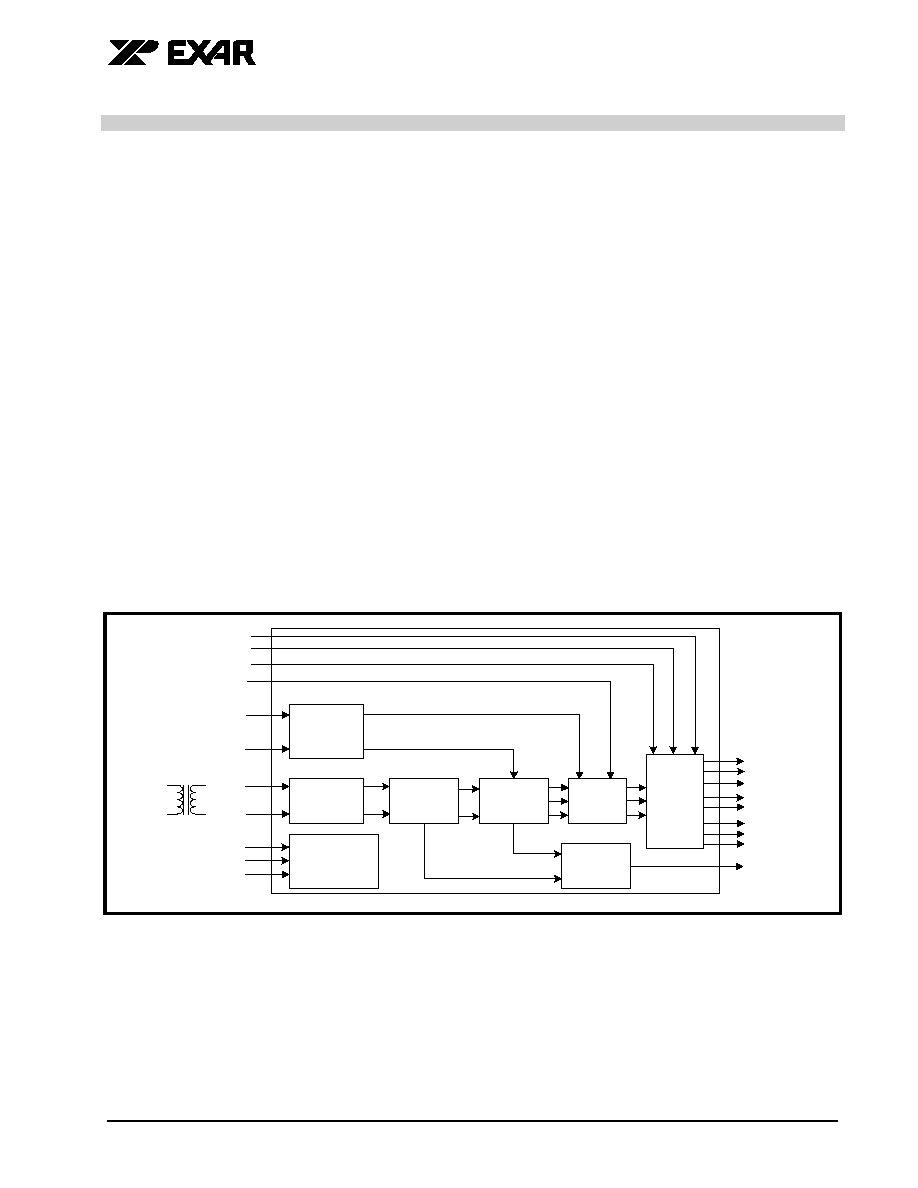
F
IGURE
1. B
LOCK
D
IAGRAM
OF
THE
XRT85L61
Master Clock
Generator
Rx
Equalizer
MCLK1
(1.544 MHz for T1)
MCLK2
(2.048 MHz for E1
or 64 kbps)
Reference Inputs
RTIP
RRING
Line Side
Peak Detector
and Slicer
Clock and
Data
Recovery
Jitter
Attenuator
Clock
Extractor
Line code
and clock
violation
Detector
RPOS
RNEG
RCLK
(64kHz,1544kHz or 2048kHz)
8 kHz
(for 64 kbps)
400 Hz
(for 64 kbps)
RCLK_LCV/AIS
8 kHz_LCV/BPV
400 Hz_LCV
LOS
Detector
RLOS
Mode Select
T1, E1 or 64 kbps
S1
S2
S3
(T1 or E1 or 64 kbps input)
JAEN
DATAMUT
DATA_INV
RCLKINV

XRT85L61
BITS (BUILDING INTEGRATED TIMING SUPPLY) CLOCK EXTRACTOR
REV. 1.0.1
2
ORDERING INFORMATION
P
ART
N
UMBER
P
ACKAGE
O
PERATING
T
EMPERATURE
R
ANGE
XRT85L61IG
28 Lead TSSOP
-40
∞
C to +85
∞
C
F
IGURE
2. P
IN
O
UT
OF
THE
XRT85L61
MCLK1
MCLK2
JAEN
JAVDD
JAGND
ICT
RTIP
RRING
AVDD
AGND
S1
S2
S3
NC
RCLKINV
DATA_LCV
RCLK_LCV
8 KHz_LCV
400 Hz_LCV
8 KHz
400 Hz
RLOS
DVDD
DGND
RCLK
RPOS
RNEG
DATMUT
1
2
9
13
12
11
10
8
7
6
5
4
3
14
28
27
20
16
17
18
19
21
22
23
24
25
26
15
MCLK1
JAEN
MCLK2
JAVDD
JAGND
ICT
RTIP
RRING
AVDD
AGND
S1
S2
S3
NC
RCLKINV
DATA_INV
RCLK_LCV/ AIS
8 KHz_LCV/ BPV
400 Hz_LCV
8 KHz
400 Hz
RLOS
DVDD
DGND
RCLK
RPOS
RNEG
DATMUT
1
2
9
13
12
11
10
8
7
6
5
4
3
14
28
27
20
16
17
18
19
21
22
23
24
25
26
15

XRT85L61
BITS (BUILDING INTEGRATED TIMING SUPPLY) CLOCK EXTRACTOR
REV. 1.0.1
I
TABLE OF CONTENTS
GENERAL DESCRIPTION .................................................................................................1
A
PPLICATIONS
................................................................................................................................................1
F
IGURE
1. B
LOCK
D
IAGRAM
OF
THE
XRT85L61 ............................................................................................................................... 1
ORDERING INFORMATION .....................................................................................................................2
F
IGURE
2. P
IN
O
UT
OF
THE
XRT85L61............................................................................................................................................ 2
T
ABLE
OF
C
ONTENTS
............................................................................................................I
PIN DESCRIPTIONS ..........................................................................................................3
ELECTRICAL CHARACTERISTICS ..................................................................................6
A
BSOLUTE
M
AXIMUM
R
ATINGS
............................................................................................................. 6
DC Electrical Characteristics ....................................................................................................................6
FUNCTIONAL DESCRIPTION ...........................................................................................7
1.0 OPERATING MODE: ..............................................................................................................................7
1.1 64 KHZ CLOCK MODE: .................................................................................................................................... 7
T
ABLE
1: O
PERATING
M
ODE
S
ELECTION
........................................................................................................................................... 7
T
ABLE
2: G.703 S
PECIFICATION
FOR
THE
64
K
H
Z
CLOCK
SIGNAL
AT
INPUT
PORT
............................................................................... 7
1.1.1 64 KHZ + 8 KHZ CLOCK EXTRACTION ...................................................................................................................... 8
1.1.2 64 KHZ + 8 KHZ + 400 HZ CLOCK EXTRACTION ...................................................................................................... 8
T
ABLE
3: G.703 S
PECIFICATION
FOR
THE
64
K
H
Z
CLOCK
SIGNAL
AT
OUTPUT
PORT
............................................................................ 8
F
IGURE
3. I
NPUT
D
ATA
64
K
H
Z
+ 8
K
H
Z
O
PERATION
(
S
1 = 0,
S
2 = 0,
S
3 = 0) ................................................................................... 8
1.2 2048 KHZ RZ E1 MODE ................................................................................................................................... 9
F
IGURE
4. I
NPUT
D
ATA
64
K
H
Z
+ 8
K
H
Z
+ 400 H
Z
O
PERATION
(
S
1 = 0,
S
2 = 0,
S
3 = 1) ................................................................... 9
F
IGURE
5. E1 P
ULSE
M
ASK
(G.703) ................................................................................................................................................ 9
T
ABLE
4: G.703 S
PECIFICATION
E1................................................................................................................................................ 10
1.3 2048 KHZ NRZ MODE .................................................................................................................................... 11
F
IGURE
6. E1 C
LOCK
S
IGNAL
W
AVE
S
HAPE
- G.703 ...................................................................................................................... 11
T
ABLE
5: G.703 2048
K
H
Z
C
LOCK
I
NTERFACE
............................................................................................................................... 11
1.4 1544 KHZ T1 MODE ....................................................................................................................................... 12
F
IGURE
7. G.703 DS1 W
AVE
F
ORM
............................................................................................................................................... 12
2.0 AIS DETECTION TIMING ....................................................................................................................13
F
IGURE
8. AIS D
ETECTION
FOR
E1 M
ODE
...................................................................................................................................... 13
F
IGURE
9. AIS D
ETECTION
FOR
T1 M
ODE
...................................................................................................................................... 13
ORDERING INFORMATION ...................................................................................................................14
R
EVISION
H
ISTORY
............................................................................................................................. 15
XRT85L61
BITS (BUILDING INTEGRATED TIMING SUPPLY) CLOCK EXTRACTOR
REV. 1.0.1
3
PIN DESCRIPTIONS
P
IN
#
S
YMBOL
T
YPE
D
ESCRIPTION
1
MCLK1
I
Reference T1 Clock input:
This signal is an independent 1544 kHz clock with accuracy better than
+ 32 ppm and duty cycle within 40% to 60%. This clock provides timing
source for the PLL clock recovery circuit in T1 mode.
N
OTE
: If T1 mode is not used, this clock is not necessary for the device
to operate.
2
JAEN
I
Jitter Attenuator Enable:
Tie this pin "High" to enable the Jitter Attenuator. When enabled, a 32 bit
FIFO is included in the data path for all modes of operation.
N
OTE
: Internally Pulled down with 50 k
resistor
3
MCLK2
I
Reference E1 and 64 kHz Clock Input:
This signal is an independent 2048 kHz clock with accuracy better than +
50 ppm and duty cycle within 40% to 60%. This clock provides timing
source for the PLL clock recovery circuit in E1 and 64 kHz mode.
N
OTE
: To reduce intrinsic jitter when the JA is enabled, it is
recommended to have a reference clock with an accuracy of ±
25 ppm or better. If E1 mode or 64 kHz mode is not used, this
clock is not necessary for the device to operate.
4
JAVDD
***
VDD for Jitter Attenuator (3.3V ± 5%)
5
JAGND
***
Jitter Attenuator Ground
6
ICT
I
In circuit Testing
When this pin is grounded, all output pins are Tri-stated for testing pur-
poses.
N
OTE
: Internally Pulled up with 50 k
resistor
7
RTIP
I
Receive Positive Input
8
RRING
I
Receive Negative Input
9
AVDD
***
Analog VDD (3.3V ± 5%)
10
AGND
***
Analog Ground

XRT85L61
BITS (BUILDING INTEGRATED TIMING SUPPLY) CLOCK EXTRACTOR
REV. 1.0.1
4
11
S1
I
Mode Select
N
OTE
: T1 NRZ or E1 NRZ means the output data at RPOS and RNEG
are 1 RCLK wide.
12
S2
I
Mode Select
13
S3
I
Mode Select
14
NC
***
This pin must be grounded for normal operation
15
DATMUT
I
Data Muting:
Connect this pin "High" to mute data output to "Low" state at RPOS/
RNEG. The RLOS pin can be connected to this pin to mute the output
when RLOS occurs.
N
OTE
: Internally Pulled down with 50 k
resistor
16
RNEG
O
Receive Negative Data Output:
The data is half clock cycle wide.
17
RPOS
O
Receive Positive Data Output:
The data is half clock cycle wide
18
RCLK
O
Receive Clock Output
Outputs either 1.544 MHz or 2.048 MHz or 64 kHz clock
19
DGND
***
Digital Supply Ground
20
DVDD
***
Digital Supply Voltage (3.3V ± 5%)
21
RLOS
O
Receive Loss of Signal Output
22
400Hz
O
400 Hz Clock output for 64 kHz Operation
23
8 kHz
O
8 kHz clock output for 64 kHz Operation
24
400Hz_LCV
O
Line Code Violation for 400 Hz
This pin will stay "High" when 400 Hz is not in sync.
PIN DESCRIPTIONS
P
IN
#
S
YMBOL
T
YPE
D
ESCRIPTION
S2
S3
0
0
0
1
1
0
1
1
MODE
64 kHz + 8 kHz
64kHz+8kHz+400Hz
E1 RZ
E1 NRZ
S1
0
0
0
0
0
0
0
1
1
1
1
T1
T1
(output full width data)
E1
(output full width data)
Reserved
1
1
1
1
0

XRT85L61
BITS (BUILDING INTEGRATED TIMING SUPPLY) CLOCK EXTRACTOR
REV. 1.0.1
5
25
8 kHz_LCV/
BPV
O
Line Code Violation for 8 kHz in 64 kHz operation
Bipolar Violation:
In E1RZ or T1 mode, every Bipolar violation valid or not valid is indicated
at this pin.
This pin will stay "High" when 8 kHz is not in sync.
26
RCLK_LCV/AIS
O
Receive Clock Violation.
In 64 kbps operation, every missing pulse will cause this pin to go "High"
for half the clock cycle
AIS Indication
In E1RZ or T1 mode, this output serves as an AIS indicator. AIS will stay
"High" for 250
µ
s in E1 RZ mode, and in T1 mode, AIS will stay "High" for
3 ms.
27
DATA_INV
I
Data Invert:
Connect this pin "High" to output active "Low" data at RPOS/RNEG.
N
OTE
: Internally Pulled down with 50 k
resistor
28
RCLK_INV
I
Receive Clock Invert:
Connect this pin "High" to align the data to change at the falling edge of
RCLK.
N
OTE
: Internally Pulled down with 50 k
resistor
PIN DESCRIPTIONS
P
IN
#
S
YMBOL
T
YPE
D
ESCRIPTION

XRT85L61
BITS (BUILDING INTEGRATED TIMING SUPPLY) CLOCK EXTRACTOR
REV. 1.0.1
6
ELECTRICAL CHARACTERISTICS
N
OTE
: * Not applicable to pins with pull-down resistors.
ABSOLUTE MAXIMUM RATINGS
Storage Temperature
- 65∞C to + 150∞C
Operating Temperature
- 40∞C to + 85∞C
Supply Voltage Range
-0.5V to +6.0V
ESD
2000 V
Theta-JA
68∞C/W
Theta-JC
13∞C/W
E
LECTRICAL
C
HARACTERISTICS
(T
A
= 25
∞
C, V
DD
= 3.3 V + 5%,
UNLESS
OTHERWISE
SPECIFIED
)
S
YMBOL
P
ARAMETER
M
IN
.
TYP
.
M
AX
.
U
NITS
DC Electrical Characteristics
V
DDD
DC Supply Voltage (Digital)
3.135
3.3
3.465
V
V
DDA
DC Supply Voltage (Analog)
3.135
3.3
3.465
V
V
IL
Input Low Voltage
0.8
V
V
IH
Input High Voltage
2.0
V
DD
V
V
OL
Output Low Voltage, IOUT = -4.0mA
0
0.4
V
V
OH
Output High Voltage, IOUT = 4.0mA
2.4
V
DD
V
I
L
Input Leakage Current*
±10
µA
C
I
Input Capacitance
5
pF
C
L
Output Load Capacitance
25
pF
XRT85L61
BITS (BUILDING INTEGRATED TIMING SUPPLY) CLOCK EXTRACTOR
REV. 1.0.1
7
FUNCTIONAL DESCRIPTION
The XRT85L61 is an integrated BITS (Building Integrated Timing Supply) Clock Generator. Simplified block
diagram of the chip is shown in Figure 1.
The XRT85L61 extracts the clock signals from the following synchronization lines:
s
Balanced 100
lines with 1544 kbps DS1 pattern.
s
Balanced 120
or unbalanced 75
lines with 2048 kbps RZ pattern.
s
Balanced 120
or unbalanced 75
line with 2048 kbps NRZ pattern.
s
Balanced 110
line with 64 kbps having 8 kHz violations; a "64 kHz + 8 kHz sync pattern.
s
Balanced 110
line with a 64 kbps pattern having both 8 kHz and 400 Hz violations; a "64 kHz + 8 kHz
+ 400 Hz" sync pattern.
1.0
OPERATING MODE:
The operating mode for the XRT85L61 is shown in Table 1.
1.1
64 kHz Clock Mode:
The XRT85L61 receives the 64 kbps ternary RZ signal. Two modes of 64 kHz operation is possible by selecting
S1, S2 and S3 as shown in Table 1.
T
ABLE
1: O
PERATING
M
ODE
S
ELECTION
S1
S2
S3
MODE
D
ATA
O
UTPUT
AT
RPOS / RNEG
0
0
0
64 kHz + 8 kHz
RZ
0
0
1
64 kHz + 8 kHz + 400 Hz
RZ
0
1
0
E1RZ
RZ
0
1
1
E1NRZ
RZ
1
0
0
T1
RZ
1
0
1
T1 (full width)
1
1
0
E1 (full width)
1
1
1
Reserved
T
ABLE
2: G.703 S
PECIFICATION
FOR
THE
64
K
H
Z
CLOCK
SIGNAL
AT
INPUT
PORT
F
REQUENCY
(
A
) 64
K
H
Z
+ 8
K
H
Z
OR
(
B
) 64
K
H
Z
+ 8
K
H
Z
+ 400 H
Z
Signal Format
(a) AMI with 8 kHz Bipolar Violation
(b) AMI with 8 kHz Bipolar Violation removed at every 400 Hz.
Alarm Condition
Alarm should not occur against the amplitude range from 0.63 V to 1.1 V

XRT85L61
BITS (BUILDING INTEGRATED TIMING SUPPLY) CLOCK EXTRACTOR
REV. 1.0.1
8
1.1.1
64 kHz + 8 kHz Clock Extraction
The input data is shown in Figure 3. The 64 kHz clock signal consist of AMI code with 8 kHz Bipolar Violation.
Both the 64 kHz and 8 kHz components are extracted from the composite received signal and presented at the
64 kHz and 8 kHz output pins.
1.1.2
64 kHz + 8 kHz + 400 Hz Clock Extraction
Figure 4 shows the input data for this mode. The 64 kHz clock signal consist of AMI code with 8 kHz Bipolar
Violation removed every 400 Hz. The 64 kHz, 8 kHz and 400 Hz components are extracted from the composite
received signal and presented at the RClk, 8 kHz and 400 Hz output pins.
N
OTE
: The inputs are not aligned with all output signals. The above diagram is used to depict the output activity when the
input signals have errors.
T
ABLE
3: G.703 S
PECIFICATION
FOR
THE
64
K
H
Z
CLOCK
SIGNAL
AT
OUTPUT
PORT
F
REQUENCY
(
A
) 64
K
H
Z
+ 8
K
H
Z
OR
(
B
) 64
K
H
Z
+ 8
K
H
Z
+ 400 H
Z
Load Impedance
110
resistive
Transmission Media
Symmetric Pair Cable
Pulse Width (FWHM)
< 7.8 ± 0.78
µ
s
Amplitude
< 1 V ± 0.1 V
F
IGURE
3. I
NPUT
D
ATA
64
K
H
Z
+ 8
K
H
Z
O
PERATION
(
S
1 = 0,
S
2 = 0,
S
3 = 0)
V
V
V
V
RTIP/
RRING
64kHz
Clock
RPOS
RNEG
8kHz Clock
RClk_LCV
8kH_LCV
Missing Pulse
Missing Pulse or Wrong Polarity Pulse
Missing Pulse
Missing Pulse
Missing Pulse
Not Valid Violation
Not Valid Violation
Missing Pulse or No Violation Bit
If Pulse Missing at RTIP/RRING
out of sync
XRT85L61
BITS (BUILDING INTEGRATED TIMING SUPPLY) CLOCK EXTRACTOR
REV. 1.0.1
9
N
OTES
:
1.
V1 and V2 indicate AMI code-rule violations, and give the 8kHz timing.
2.
V1 and V2 have different violation polarity with respect to each other.
3.
nV indicates no violation (violation stealing) and gives the 400 Hz timing.
1.2
2048 kHz RZ E1 Mode
In this mode, the XRT85L61 receives a standard E1 signal as shown in Figure 5. Table 4 gives the details of
the E1 pulse.
F
IGURE
4. I
NPUT
D
ATA
64
K
H
Z
+ 8
K
H
Z
+ 400 H
Z
O
PERATION
(
S
1 = 0,
S
2 = 0,
S
3 = 1)
F
IGURE
5. E1 P
ULSE
M
ASK
(G.703)
V1
125
µ
s
(8 kH z)
125
µ
s
(8 kH z)
125
µ
s
(8 kH z)
125
µ
s
(8 kH z)
nV
V2
V1
V2
nV
(8 kH z)
(400 H z)
(400 H z)
L C V
if nV is
Missing
10%
10%
10%
10%
10%
10%
2 6 9 n s
(2 4 4 + 2 5 )
1 9 4 n s
(2 4 4 ≠ 5 0 )
2 4 4 n s
2 1 9 n s
(2 4 4 ≠ 2 5 )
4 8 8 n s
(2 4 4 + 2 4 4 )
0 %
5 0 %
20%
V = 1 0 0 %
N o m in a l p u l s e
N o te ≠ V c o rre s p o n d s t o t h e n o m in al p ea k v a lu e .
20%
20%

XRT85L61
BITS (BUILDING INTEGRATED TIMING SUPPLY) CLOCK EXTRACTOR
REV. 1.0.1
10
T
ABLE
4: G.703 S
PECIFICATION
E1
P
ULSE
I
NTERFACE
Pulse Shape (nominally rectangular)
All Marks of a valid signal must conform with the mask irrespective of
the sign. The value V corresponds to the nominal peak value.
Pair(s) in each direction
One coaxial pair
One symmetrical pair
Test Load Impedance
75
Resistive
120
Resistive
Nominal peak voltage of a mark (pulse)
2.37 V
3 V
Peak voltage of a space (no pulse)
0 ± 0.237 V
0 ± 0.3 V
Nominal Pulse Width
244 ns
Ratio of the amplitudes of positive and negative
pulses at the center of the pulse interval
0.95 to 1.05
Ratio of the widths of positive and negative
pulses at the nominal half amplitude
0.95 to 1.05
Maximum peak to peak jitter at an output port
Refer to ITU-T G.823 specification

XRT85L61
BITS (BUILDING INTEGRATED TIMING SUPPLY) CLOCK EXTRACTOR
REV. 1.0.1
11
1.3
2048 kHz NRZ Mode
In this mode, XRT85L61 receives 2048 kbps synchronization signal as shown in Figure 6.
F
IGURE
6. E1 C
LOCK
S
IGNAL
W
AVE
S
HAPE
- G.703
T
ABLE
5: G.703 2048
K
H
Z
C
LOCK
I
NTERFACE
P
ULSE
I
NTERFACE
Frequency
2048 kHz ± 50 ppm
Pulse Shape
The signal must conform with the mask.
The value V corresponds to maximum peak value
The value V
1
corresponds to minimum peak value
Pair(s) in each direction
Coaxial pair
Symmetrical pair
Test Load Impedance
75
Resistive
120
Resistive
Maximum peak value (V
op
)
1.5
1.9
Minimum peak value (V
op
)
0.75
1.0
Maximum jitter at an output port
0.05 UI peak to peak measured within the frequency range f
1
= 20 Hz
to f
4
= 100 kHz
N
OTE
: This value is valid for network timing distribution equipment.
Other values may be specified for timing output ports of digital
links carrying the network timing.
T
3 0
T
3 0
T
3 0
T
3 0
T
3 0
T
3 0
T
4
T
4
T
4
T
4
T
+ V
+ V
≠ V
≠ V
0
1
1
T 1 8 1 8 9 0 0 - 9 2
S h a d e d a r e a in w h i c h
s ig n a l s h o u l d b e
m o n o to n ic
T A v e r a g e p e ri o d o f
s y n c h r o n i z in g s ig n a l
F IG U R E 2 1 /G .7 0 3
W a v e s h a p e a t a n o u tp u t p o rt

XRT85L61
BITS (BUILDING INTEGRATED TIMING SUPPLY) CLOCK EXTRACTOR
REV. 1.0.1
12
1.4
1544 kHz T1 Mode
In this mode, the XRT85L61 receives a standard DS1 signal as shown in Figure 7.
F
IGURE
7. G.703 DS1 W
AVE
F
ORM
T 1 5 2 86 7 0 -9 8
N o r m aliz ed a m p litu d e
T im e , in U n it In te rv als
1 .5
1 .0
0 .5
0
≠ 0 .5
≠ 1 .0
1 .5
1 .0
0 .5
0
≠ 0.5
≠ 1 .0

XRT85L61
BITS (BUILDING INTEGRATED TIMING SUPPLY) CLOCK EXTRACTOR
REV. 1.0.1
13
2.0
AIS DETECTION TIMING
In E1 mode, AIS is set when the incoming signal has 2 or less Zeros in sequence of 512 bits. AIS will stay
"High" for 250
µ
s and AIS is cleared upon receiving three or more zeros in the subsequent 512 bits (250
µ
s)
time-frame. Figure 8 shows the AIS timing.
In T1 mode, AIS is cleared when 5 or more zeros is detected in the subsequent 4632 bits (3 ms) time-frame.
Figure 9 shows the AIS timing for T1 mode.
F
IGURE
8. AIS D
ETECTION
FOR
E1 M
ODE
F
IGURE
9. AIS D
ETECTION
FOR
T1 M
ODE
E1
DATA
AIS
250
µ
s
250
µ
s
0
0
0
0
0
3 ms
3 ms
T1
DATA
AIS
0
0
0
0
0
0
0
0
0
0

XRT85L61
BITS (BUILDING INTEGRATED TIMING SUPPLY) CLOCK EXTRACTOR
REV. 1.0.1
14
PACKAGE OUTLINE DRAWING
ORDERING INFORMATION
P
ART
N
UMBER
P
ACKAGE
O
PERATING
T
EMPERATURE
R
ANGE
XRT85L61IG
28 Lead TSSOP
-40
∞
C to +85
∞
C
e
D
B
A
1
28
15
14
1
A
L
C
A
2
E
1
E
S eatin g
P lane
S Y M B O L
M IN
M A X
M IN
M A X
A
0 .0 3 3
0 .0 4 7
0 .8 5
1 .2 0
A 1
0 .0 0 2
0 .0 0 6
0 .0 5
0 .1 5
A 2
0 .0 3 1
0 .0 4 1
0 .8 0
1 .0 5
B
0 .0 0 7
0 .0 1 2
0 .1 9
0 .3 0
C
0 .0 0 4
0 .0 0 8
0 .0 9
0 .2 0
D
0 .3 7 8
0 .3 8 6
9 .6 0
9 .8 0
E
0 .2 4 8
0 .2 6 0
6 .3 0
6 .6 0
E 1
0 .1 6 9
0 .1 7 7
4 .3 0
4 .5 0
e
0 .0 2 5 6 B S C
0 .6 5 B S C
L
0 .0 1 8
0 .0 3 0
0 .4 5
0 .7 5
0 ∞
8 ∞
0 ∞
8 ∞
M IL L IM E T E R S
IN C H E S
N o te : T h e co n tro l d im e n sio n is in th e m illim e te r co lu m n

XRT85L61
BITS (BUILDING INTEGRATED TIMING SUPPLY) CLOCK EXTRACTOR
REV. 1.0.1
15
NOTICE
EXAR Corporation reserves the right to make changes to the products contained in this publication in order
to improve design, performance or reliability. EXAR Corporation assumes no responsibility for the use of
any circuits described herein, conveys no license under any patent or other right, and makes no
representation that the circuits are free of patent infringement. Charts and schedules contained here in are
only for illustration purposes and may vary depending upon a user's specific application. While the
information in this publication has been carefully checked; no responsibility, however, is assumed for
inaccuracies.
EXAR Corporation does not recommend the use of any of its products in life support applications where
the failure or malfunction of the product can reasonably be expected to cause failure of the life support
system or to significantly affect its safety or effectiveness. Products are not authorized for use in such
applications unless EXAR Corporation receives, in writing, assurances to its satisfaction that: (a) the risk of
injury or damage has been minimized; (b) the user assumes all such risks; (c) potential liability of EXAR
Corporation is adequately protected under the circumstances.
Copyright 2004 EXAR Corporation
Datasheet February 2004.
REVISION HISTORY
R
EVISION
#
D
ATE
C
HANGES
P1.0.1
August 2002
original
P1.0.2
November 2002
Edits to text
P1.0.3
December 2002
Ordering information changed from XRT85L61IV to XRT85L61IG
1.0.0
January 2004
Final Release
1.0.1
February 2004
Added description for MCLK1 and MCLK2.