Exar
Corporation 48720 Kato Road, Fremont CA, 94538
�
(510) 668-7000
�
FAX (510) 668-7017
�
www.exar.com
PRELIMINARY
XRT91L81
2.488/2.666GBPS OC-48/STM-16 SONET/SDH TRANSCEIVER
JANUARY 2004
REV. P1.0.3
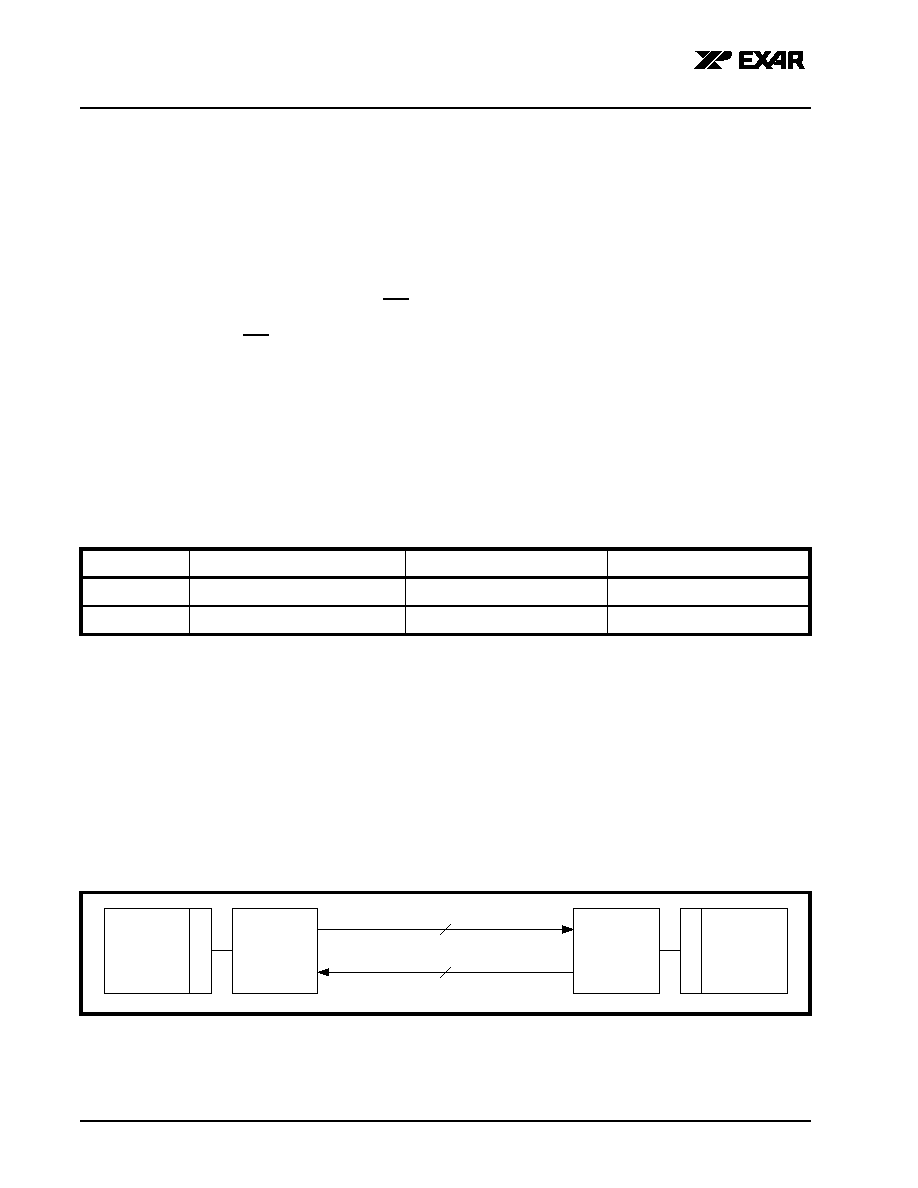
GENERAL DESCRIPTION
The XRT91L81 is a fully integrated SONET/SDH
transceiver block for applications in SONET OC-48
allowing the use of Forward Error Correction (FEC)
capability. The transceiver includes an on-chip Clock
Multiplier Unit (CMU), which uses a high frequency
Phase-Locked Loop (PLL) to generate the high-
speed transmit serial clock from slower external clock
references. It also provides Clock and Data Recovery
(CDR) functions by synchronizing its on-chip Voltage
Controlled Oscillator (VCO) to the incoming serial
data stream. The chip provides serial-to-parallel and
parallel-to-serial converters and 4-bit LVDS system
interfaces in both receive and transmit directions.
The transmit section includes a 4x9 Elastic Buffer
(FIFO) to absorb any phase differences between the
transmitter input clock and the internally generated
transmitter reference clock. In the event of an
overflow, an internal FIFO control circuit outputs an
OVERFLOW indication. The FIFO under the control
of the AUTORST pin can automatically recover from
an overflow condition. The operation of the device
can be monitored by checking the status of the
LOCKDET and LOSDET output signals. An on-chip
phase/frequency detector and charge-pump offers
the ability to form a de-jittering PLL with an external
VCXO that can be used in loop timing mode to clean
up the recovered clock in the receive section.
APPLICATIONS
�
SONET/SDH-based Transmission Systems
�
Add/Drop Multiplexers
�
Cross Connect Equipment
�
ATM and Multi-Service Switches, Routers and
Switch/Routers
�
DSLAMS
�
SONET/SDH Test Equipment
�
DWDM Termination Equipment
�
Optical Modules and Sub-Systems
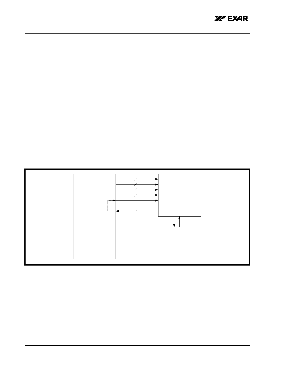
F
IGURE
1. B
LOCK
D
IAGRAM
OF
THE
XRT91L81
PISO
(Parallel Input
Serial Output)
PFD
& Charge Pump
TxDI0P/N
SC
L
K
SD
I
Serial
Microprocessor
Hardware
Control
IN
T
SD
O
Re
se
t
H
o
s
t/H
w
R
L
OOP
S
DLO
O
P
R
L
OOP
P
LP
T
I
M
E
_J
A
LP
T
M
_NO
_
J
A
TxDI1P/N
TxDI2P/N
TxDI3P/N
TxCLKIP/N
DLOOP
RLOOPP
RxDO0P/N
RxDO1P/N
RxDO2P/N
RxDO3P/N
RxCLKP/N
4
x
9
FI
FO
W P
RP
SIPO
(Serial Input
Parallel Output)
RLOOPS
CDR
Re-Timer
CMU
TXOP/N
TXO2P/N
TXO2DIS
TXO2SEL
RXI0P/N
RXI1P/N
RXSEL
R
E
F
C
L
KP/
N
VC
XO
_
I
N
P
/
N
R
E
FFR
E
Q
S
E
L
VC
XO
_
SEL
VC
XO
_
L
O
C
KE
N
VC
XO
_
L
O
C
K
CP
O
U
T
L
O
O
PBW
TXPCLKOP/N
TXCLKO16P/N
TRITXCLKO16
LO
C
K
DE
T
_
CM
U
OV
E
R
FLOW
FIFO_RST
FIFO_AUTORST
TRIRXD
REXT
RXCLK16P/N
LO
CK
DE
T
_
CDR
L
O
SD
ET
L
O
SEXT
PO
L
A
R
I
T
Y
DISRD
0
1
0
1
OC-48 TRANSCEIVER
CS
T
EST
XRT91L81
2.488/2.666GBPS OC-48/STM-16 SONET/SDH TRANSCEIVER
REV. P1.0.3
PRELIMINARY
2
FEATURES
�
2.488 / 2.666 Gbps Transceiver
�
Single-chip fully integrated solution containing
parallel-to-serial converter, clock multiplier unit
(CMU), serial-to-parallel converter, limiting amplifier
and clock data recovery (CDR) functions
�
Host mode serial microprocessor interface
simplifies monitor and control
�
Provides support for dual fiber rings
�
Integrated limiting amplifier accepts differential
inputs down to 10mVp-p
�
Separate reference and VCXO input ports support
multiple de-jittering modes
�
On-chip phase detector and charge pump for
external VCXO based de-jittering PLL
�
Targeted for SONET OC-48/SDH STM-16
Applications
�
Selectable full duplex operation between standard
rate of 2.488 Gbps or Forward Error Correction rate
of 2.666 Gbps
�
4-bit LVDS data paths at 622/666 MHz complies
with OIF SFI-4 Implimentation Agreement
�
Internal FIFO decouples transmit input and output
clocks
�
Tx CMU and Rx CDR lock detect
�
Provides Local, Remote and Split Loop-Back
modes as well as Loop Timing mode
�
Diagnostics features include various lock detect
functions
�
Meets Telcordia, ANSI and ITU-T jitter
requirements
�
Operates at 1.8V with 3.3V I/O
�
600mW Typical Power Dissipation
�
Package: 12 x 12 mm 196-pin STBGA
PRODUCT ORDERING INFORMATION
P
RODUCT
N
UMBER
P
ACKAGE
T
YPE
O
PERATING
T
EMPERATURE
R
ANGE
XRT91L81IB
196 STBGA
-40�C to +85�C

XRT91L81
2.488/2.666GBPS OC-48/STM-16 SONET/SDH TRANSCEIVER
PRELIMINARY
REV. P1.0.3
3
T
ABLE
1: 196 BGA P
INOUT
OF
THE XRT91L81 (T
OP
V
IEW
)
RX
D3
P
RXD3
N
RX
D1
P
RXD1
N
RX
C
L
K
P
RXC
L
K
N
DGND
TX
C
L
K
I
P
TX
C
L
KI
N
TX
D
I
1
P
TXD
I
1
N
TX
D
I
3
P
TXD
I
3
N
VDD3
.3
14
V
DD3
.3
V
DD3
.3
RXD2
P
RX
D2
N
RXD0
P
RX
D0
N
DGND
TX
D
I
0P
TX
D
I
0N
TX
D
I
2P
TX
D
I
2N
O
VER
FL
O
W
FI
F
O
_
R
ESE
T
V
DD3
.3
13
DG
N
D
DG
N
D
TR
I
R
X
D
VDD1
.8
VDD1
.8
DG
N
D
DG
N
D
DG
N
D
DG
N
D
DG
N
D
DG
N
D
T
R
IT
X
C
L
K
O1
6
FI
F
O
_A
U
T
O
R
S
T
DG
N
D
12
RLOOP
P
DGND
INT
B
VDD
3
.
3
VDD
3
.
3
DGND
DGND
DGND
DGND
VDD
1
.
8
DGND
VDD
1
.
8
TX
C
L
K
O
16
N
TX
PC
L
K
O
N
11
CSB
Re
set
RL
O
O
P
S
V
DD3
.3
TG
N
D
TG
N
D
TG
N
D
TG
N
D
TG
N
D
TG
N
D
V
DD1
.8
V
DD1
.8
TX
C
L
K
O
16P
TXP
C
L
K
O
P
10
SD
I
SCL
K
HOS
T
/HWB
VDD3
.3
TG
N
D
TG
N
D
TG
N
D
TG
N
D
TG
N
D
TG
N
D
VDD1
.8
VDD1
.8
A
V
DD1
.8
_
T
X
A
V
DD3
.3
_
T
X
9
V
DD3
.3
DGND
SDO
A
V
DD1
.8
_
R
X
TG
N
D
TG
N
D
TG
N
D
TG
N
D
TG
N
D
TG
N
D
A
V
DD1
.8
_
T
X
NC
VC
XO
_
L
O
C
K
CP
OUT
8
RX
CL
K1
6
N
VDD
1
.
8
L
O
CK
DET
-
CD
R
AGND_
RX
TG
N
D
TG
N
D
TG
N
D
TG
N
D
TG
N
D
TG
N
D
A
V
D
D
1
.
8_T
X
LO
OP
B
W
A
G
ND_
T
X
A
G
ND_
T
X
7
RX
CL
K1
6
P
DL
O
O
P
LP
T
I
ME
_JA
A
V
DD1
.8
_
R
X
TG
N
D
TG
N
D
TG
N
D
TG
N
D
TG
N
D
TG
N
D
A
V
DD1
.8
_
T
X
V
C
XO
_
SEL
REF
C
L
K
N
REF
C
L
K
P
6
DGND
L
O
SE
XT
L
O
SDET
A
V
DD1
.8
_
R
X
TG
N
D
TG
N
D
TG
N
D
TG
N
D
TG
N
D
TG
N
D
AGND_
T
X
AGND_
T
X
AGND_
T
X
A
V
DD3
.3
_
T
X
5
DGND
DGND
PO
L
A
RI
T
Y
A
V
DD1
.8
_
R
X
AGND_
RX
AGND_
RX
AGND_
RX
AGND_
RX
A
V
DD1
.8
_
T
X
A
G
ND_
T
X
A
G
ND_
T
X
A
G
ND_
T
X
VCXO
_
I
NN
VC
XO
_
I
NP
4
DISRD
DGND
AGND_
RX
A
V
DD3
.3
_
R
X
A
V
DD3
.3
_
R
X
A
V
DD1
.8
_
R
X
A
V
DD1
.8
_
R
X
AGND_
RX
AGND_
T
X
AGND_
T
X
DGND
A
V
DD1
.
8
_
T
X
T
X
O
2
_
SEL
V
C
XO
_
L
O
CK
EN
3
RXS
E
L
AGND_
RX
AGND_
RX
AGND_
RX
AGND_
RX
AGND_
RX
AGND_
RX
AGND_
RX
AGND_
T
X
TX
O
N
TX
O
P
A
V
DD3
.
3
_
T
X
L
O
CKDET
-
CM
U
LP
TI
M
E
_
N
O
_
J
A
2
REX
T
AGND_
RX
RX
I0
P
RXI0
N
AGND_
RX
RXI1
N
RX
I1
P
AGND_
RX
A
V
D
D
3
.
3_T
X
TX
O
2
P
TX
O
2
N
AGND_
T
X
TX
O
2
D
I
S
REF
F
R
E
Q
SEL
1
A
B
C
D
E
F
G
H
J
K
L
M
N
P

XRT91L81
2.488/2.666GBPS OC-48/STM-16 SONET/SDH TRANSCEIVER
REV. P1.0.3
PRELIMINARY
I
TABLE OF CONTENTS
GENERAL DESCRIPTION .................................................................................................1
APPLICATIONS ...........................................................................................................................................1
F
IGURE
1. B
LOCK
D
IAGRAM
OF
THE
XRT91L81 ............................................................................................................................... 1
FEATURES
......................................................................................................................................................2
PRODUCT ORDERING INFORMATION ..................................................................................................2
T
ABLE
1: 196 BGA P
INOUT
OF
THE XRT91L81 (T
OP
V
IEW
) ........................................................................................................... 3
T
ABLE
OF
C
ONTENTS
............................................................................................................I
PIN DESCRIPTIONS ..........................................................................................................4
S
ERIAL
M
ICROPROCESSOR
INTERFACE
............................................................................................................4
H
ARDWARE
CONTROL
.....................................................................................................................................5
T
RANSMITTER
S
ECTION
..................................................................................................................................6
RECEIVER
SECTION
.........................................................................................................................................8
P
OWER
AND
G
ROUND
..................................................................................................................................10
N
O
C
ONNECTS
.............................................................................................................................................11
1.0 FUNCTIONAL DESCRIPTION .............................................................................................................12
1.1 HARDWARE MODE VS. HOST MODE .......................................................................................................... 12
1.2 INPUT CLOCK REFERENCE ......................................................................................................................... 12
1.3 FORWARD ERROR CORRECTION (FEC) .................................................................................................... 12
T
ABLE
2: R
EFERENCE
F
REQUENCY
O
PTIONS
(N
ORMAL
M
ODE
/FEC) ................................................................................................ 12
F
IGURE
2. S
IMPLIFIED
B
LOCK
D
IAGRAM
OF
F
ORWARD
E
RROR
C
ORRECTION
.................................................................................... 12
2.0 RECEIVE SECTION .............................................................................................................................13
2.1 RECEIVE SERIAL INPUT ............................................................................................................................... 13
F
IGURE
3. R
ECEIVE
S
ERIAL
I
NPUT
I
NTERFACE
B
LOCK
..................................................................................................................... 13
2.2 RECEIVE CLOCK AND DATA RECOVERY .................................................................................................. 14
2.3 LOSS OF SIGNAL .......................................................................................................................................... 14
2.4 RECEIVE SERIAL INPUT TO PARALLEL OUTPUT (SIPO) ......................................................................... 14
F
IGURE
4. S
IMPLIFIED
B
LOCK
D
IAGRAM
OF
SIPO ........................................................................................................................... 14
2.5 RECEIVE PARALLEL OUTPUT INTERFACE ............................................................................................... 15
2.6 RECEIVE PARALLEL OUTPUT DATA TIMING ............................................................................................ 15
F
IGURE
6. R
ECEIVE
P
ARALLEL
O
UTPUT
T
IMING
.............................................................................................................................. 15
T
ABLE
3: R
ECEIVE
P
ARALLEL
O
UTPUT
D
ATA
T
IMING
S
PECIFICATIONS
.............................................................................................. 15
2.7 DISABLE RECEIVE OUTPUT DATA UPON LOS .......................................................................................... 15
2.8 TRI-STATE RECEIVE OUTPUT DATA .......................................................................................................... 15
F
IGURE
5. R
ECEIVE
P
ARALLEL
O
UTPUT
I
NTERFACE
B
LOCK
............................................................................................................. 15
3.0 TRANSMIT SECTION ..........................................................................................................................16
3.1 TRANSMIT PARALLEL INTERFACE ............................................................................................................ 16
F
IGURE
7. T
RANSMIT
P
ARALLEL
I
NPUT
I
NTERFACE
B
LOCK
............................................................................................................... 16
3.2 TRANSMIT PARALLEL INPUT DATA TIMING .............................................................................................. 17
F
IGURE
8. T
RANSMIT
P
ARALLEL
I
NPUT
T
IMING
................................................................................................................................ 17
T
ABLE
4: T
RANSMIT
P
ARALLEL
I
NPUT
D
ATA
T
IMING
S
PECIFICATIONS
............................................................................................... 17
3.3 TRANSMIT FIFO ............................................................................................................................................. 17
3.4 FIFO CALIBRATION UPON POWER UP ....................................................................................................... 17
3.5 TRANSMIT PARALLEL INPUT TO SERIAL OUTPUT (PISO) ...................................................................... 18
3.6 CLOCK MULTIPLIER UNIT (CMU) AND RE-TIMER ..................................................................................... 18
F
IGURE
9. S
IMPLIFIED
B
LOCK
D
IAGRAM
OF
PISO ........................................................................................................................... 18
F
IGURE
10. T
RANSMIT
FIFO
AND
S
YSTEM
I
NTERFACE
.................................................................................................................... 19
3.7 LOOP TIMING AND CLOCK CONTROL ........................................................................................................ 20
T
ABLE
5: L
OOP
TIMING
AND
REFERENCE
DE
-
JITTER
CONFIGURATIONS
.............................................................................................. 20
3.8 EXTERNAL LOOP FILTER ............................................................................................................................. 21
F
IGURE
12. S
IMPLIFIED
D
IAGRAM
OF
THE
E
XTERNAL
L
OOP
F
ILTER
.................................................................................................. 21
F
IGURE
11. L
OOP
T
IMING
M
ODE
U
SING
AN
E
XTERNAL
C
LEANUP
VCXO.......................................................................................... 21
3.9 TRANSMIT SERIAL OUTPUT CONTROL ..................................................................................................... 22
F
IGURE
13. T
RANSMIT
S
ERIAL
O
UTPUT
I
NTERFACE
......................................................................................................................... 22
4.0 DIAGNOSTIC FEATURES ...................................................................................................................23
4.1 SERIAL REMOTE LOOPBACK ...................................................................................................................... 23
4.2 PARALLEL REMOTE LOOPBACK ................................................................................................................ 23
F
IGURE
14. S
ERIAL
R
EMOTE
L
OOPBACK
......................................................................................................................................... 23

XRT91L81
2.488/2.666GBPS OC-48/STM-16 SONET/SDH TRANSCEIVER
PRELIMINARY
REV. P1.0.3
II
F
IGURE
15. P
ARALLEL
R
EMOTE
L
OOPBACK
.................................................................................................................................... 23
4.3 DIGITAL LOCAL LOOPBACK ....................................................................................................................... 24
F
IGURE
16. D
IGITAL
L
OOPBACK
...................................................................................................................................................... 24
4.4 SONET JITTER REQUIREMENTS ................................................................................................................. 25
4.4.1 JITTER TOLERANCE: ................................................................................................................................................ 25
F
IGURE
17. J
ITTER
T
OLERANCE
M
ASK
............................................................................................................................................ 25
4.4.2 JITTER TRANSFER .................................................................................................................................................... 26
4.4.3 JITTER GENERATION................................................................................................................................................ 26
5.0 SERIAL MICROPROCESSOR INTERFACE BLOCK ......................................................................... 27
F
IGURE
18. S
IMPLIFIED
B
LOCK
D
IAGRAM
OF
THE
S
ERIAL
M
ICROPROCESSOR
I
NTERFACE
................................................................. 27
5.1 SERIAL TIMING INFORMATION ................................................................................................................... 27
F
IGURE
19. T
IMING
D
IAGRAM
FOR
THE
S
ERIAL
M
ICROPROCESSOR
I
NTERFACE
................................................................................ 27
5.2 16-BIT SERIAL DATA INPUT DESCRITPTION ............................................................................................. 28
5.2.1 R/W (SCLK1)............................................................................................................................................................... 28
5.2.2 A[5:0] (SCLK2 - SCLK7)............................................................................................................................................. 28
5.2.3 X (DUMMY BIT SCLK8) .............................................................................................................................................. 28
5.2.4 D[7:0] (SCLK9 - SCLK16)........................................................................................................................................... 28
5.3 8-BIT SERIAL DATA OUTPUT DESCRIPTION ............................................................................................. 28
6.0 REGISTER MAP AND BIT DESCRIPTIONS ....................................................................................... 29
T
ABLE
7: M
ICROPROCESSOR
R
EGISTER
B
IT
D
ESCRIPTION
.............................................................................................................. 29
T
ABLE
6: M
ICROPROCESSOR
R
EGISTER
M
AP
.................................................................................................................................. 29
T
ABLE
9: M
ICROPROCESSOR
R
EGISTER
B
IT
D
ESCRIPTION
.............................................................................................................. 30
T
ABLE
8: M
ICROPROCESSOR
R
EGISTER
B
IT
D
ESCRIPTION
.............................................................................................................. 30
T
ABLE
10: M
ICROPROCESSOR
R
EGISTER
B
IT
D
ESCRIPTION
............................................................................................................ 31
T
ABLE
11: M
ICROPROCESSOR
R
EGISTER
B
IT
D
ESCRIPTION
............................................................................................................ 33
T
ABLE
12: M
ICROPROCESSOR
R
EGISTER
B
IT
D
ESCRIPTION
............................................................................................................ 34
T
ABLE
13: M
ICROPROCESSOR
R
EGISTER
0
X
02
H
B
IT
D
ESCRIPTION
................................................................................................. 35
T
ABLE
14: M
ICROPROCESSOR
R
EGISTER
0
X
01
H
B
IT
D
ESCRIPTION
................................................................................................. 35
7.0 ELECTRICAL CHARACTERISTICS ................................................................................................... 36
A
BSOLUTE
M
AXIMUMS
................................................................................................................................. 36
DC E
LECTRICAL
C
HARACTERISTICS
.............................................................................................................. 36
196 S
HRINK
T
HIN
B
ALL
G
RID
A
RRAY
................................................................................................. 37
(12.0
MM
X
12.0
MM
, STBGA).......................................................................................................... 37
R
EV
. 1.00 ......................................................................................................................................... 37
ORDERING INFORMATION .................................................................................................................. 37
R
EVISION
H
ISTORY
...................................................................................................................................... 38
XRT91L81
2.488/2.666GBPS OC-48/STM-16 SONET/SDH TRANSCEIVER
REV. P1.0.3
PRELIMINARY
4
PIN DESCRIPTIONS
SERIAL MICROPROCESSOR INTERFACE
N
AME
L
EVEL
T
YPE
P
IN
D
ESCRIPTION
Host/Hw
LVTTL
I
C9
Host or Hardware Mode Select Input
The XRT91L81 offers two modes of operation for interfacing to the
device. The Host mode uses a serial microprocessor interface for
programming individual registers. The Hardware mode is controlled
by the state of the hardware pins set by the user. By default, the
device is configured in the Hardware mode.
"Low" = Hardware Mode
"High" = Host Mode
CS
LVTTL
I
A10
Chip Select Input (Host Mode Only)
Active low signal. This signal enables the serial microprocessor
interface by pulling chip select "Low". The serial microprocessor is
disabled when the chip select signal returns "High".
SCLK
LVTTL
I
B9
Serial Clock Input (Host Mode Only)
Once CS is pulled "Low", the serial microprocessor interface
requires 16 clock cycles for a complete Read or Write operation.
SDI
LVTTL
I
A9
Serial Data Input (Host Mode Only)
When CS is pulled "Low", the serial input data is sampled on the ris-
ing edge of SCLK.
SDO
LVTTL
O
C8
Serial Data Output (Host Mode Only)
If a Read function is initiated, the serial output data is updated on
the falling edge of SCLK8 through SCLK15, with the LSB (D0)
updated first. This enables the data to be sampled on the rising
edge of SCLK9 through SCLK16.
INT
LVTTL
O
C11
Interrupt Output (Host Mode Only)
Active low signal. This signal is asserted "Low" when a change in
alarm status occurs. Once the status registers have been read, the
interrupt pin will return "High".
Reset
LVTTL
I
B10
Master Reset Input
Active low signal. When this pin is pulled "Low" for more than 10
�
S,
the internal registers are set to their default state. See the register
description for the default values.

XRT91L81
2.488/2.666GBPS OC-48/STM-16 SONET/SDH TRANSCEIVER
PRELIMINARY
REV. P1.0.3
5
HARDWARE CONTROL
N
AME
L
EVEL
T
YPE
P
IN
D
ESCRIPTION
RLOOPS
LVTTL
I
C10
Serial Remote Loopback
Hardware Mode The serial remote loopback mode intercon-
nects the receive serial input data to the transmit serial output
data. If serial remote loopback is enabled, the 4-bit parallel
transmit input data is ignored while the 4-bit parallel receive out-
put data is maintained.
"Low" = Disabled
"High" = Serial Remote Loopback Mode Enabled
RLOOPP
LVTTL
I
A11
Parallel Remote Loopback
Hardware Mode The parallel remote loopback mode allows the
input serial data stream to pass through the clock and data
recovery circuit and loopback at the parallel interface to the
serial output port. The 4-bit parallel transmit input data is
ignored while the 4-bit parallel receive output data is main-
tained.
"Low" = Disabled
"High" = Parallel Remote Loopback Mode Enabled
DLOOP
LVTTL
I
B6
Digital Loopback
Hardware Mode The digital loopback mode interconnects the
4-bit parallel transmit input data and TxCLK to the 4-bit parallel
receive output data and RxCLK respectively while maintaining
the transmit serial output data. If digital loopback is enabled,
the receive serial input data is ignored.
"Low" = Disabled
"High" = Digital Loopback Mode Enabled
N
OTE
: DLOOP and RLOOPS can be enabled simultaneously
to achieve a dual loopback diagnostic feature.
LPTIME_JA
LVTTL
I
C6
Loop Timing Mode With JA
The LPTIME_JA pin must be set "High" in order to select the
recovered receive clock as the reference source for the de-jitter
PLL.
"Low" = Disabled
"High" = Enabled
LPTIME_NO_JA
LVTTL
I
P2
Loop Timing Mode With No JA
When the loop timing mode is activated the external reference
clock to the input of the CMU is replaced with the 1/16th or the
1/32nd of the high-speed recovered receive clock from the
CDR.
"Low" = Disabled
"High" = Loop timing Activated

XRT91L81
2.488/2.666GBPS OC-48/STM-16 SONET/SDH TRANSCEIVER
REV. P1.0.3
PRELIMINARY
6
TRANSMITTER SECTION
N
AME
L
EVEL
T
YPE
P
IN
D
ESCRIPTION
TXDI0P
TXDI0N
TXDI1P
TXDI1N
TXDI2P
TXDI2N
TXDI3P
TXDI3N
LVDS
I
H13
J13
K14
L14
K13
L13
M14
N14
Transmit Parallel Data Input
The 622Mbps 4-bit parallel transmit input data should be
applied to the transmitters simultaneously referenced to the ris-
ing edge of the TXCLKI input. The 4-bit parallel interface is
multiplexed into the transmit serial output interface MSB first
(TXDI3P/N).
N
OTE
: The XRT91L81 can accept 666Mbps 4-bit parallel
transmit input data for Forward Error Correction (FEC)
Applications.
TXCLKIP
TXCLKIN
LVDS
I
H14
J14
Transmit Input Clock
622MHz input clock reference for the 4-bit parallel transmit
input data TXDIP/N[3:0].
N
OTE
: The XRT91L81 can accept a 666MHz transmit input
clock for Forward Error Correction (FEC) Applications.
TXOP
TXON
CMLDIFF
O
L2
K2
Transmit Serial Data Output
The transmit serial data stream is generated by multiplexing the
4-bit parallel transmit input data into a 2.488Gbps serial data
stream. In Forward Error Correction, the transmit serial data
stream is 2.666Gbps.
TXO2P
TXO2N
CMLDIFF
O
K1
L1
Secondary Transmit Serial Data Output Port
The secondary transmit serial data port can output the TXO
serial data stream or it can output the transmit output clock.
See the pin description of TXO2_SEL and TXO2DIS for more
details.
TXO2_SEL
LVTTL
I
N3
Secondary Transmit Select
Hardware Mode The TXO2_SEL pin is used to determine the
output contents of the secondary transmit serial data output.
"Low" = 2.488Gbit/s Serial Output Data
"High" = Transmit Output Clock (2.488/2.666 GHz)
TXO2DIS
LVTTL
I
N1
Secondary Transmit Disable
Hardware Mode The TXO2DIS pin is used to disable the sec-
ondary transmit serial data output pins. If the secondary trans-
mit serial data is disabled, both TXO2P/N are pulled "High".
"Low" = TXO2 is enabled
"High" = Diabled
REFCLKP
REFCLKN
LVPECL
I
P6
N6
Reference Clock Input
This differential input clock reference is used for the transmit
clock multiplier unit (CMU) to provide the necessary high speed
clock reference for this device. Pin REFFREQSEL determines
the value used as the reference. See Pin REFFREQSEL for
more details.
VCXO_INP
VCXO_INN
LVPECL
I
P4
N4
Voltage Controled Oscillator Input
This differential input clock is used for the transmit PLL jitter
attenuation. Pin REFFREQSEL determines the value used as
the reference. See Pin REFFREQSEL for more details.

XRT91L81
2.488/2.666GBPS OC-48/STM-16 SONET/SDH TRANSCEIVER
PRELIMINARY
REV. P1.0.3
7
REFFREQSEL
LVTTL
I
P1
Reference Clock Frequency Select
Hardware Mode This pin is used to select the frequency of the
REFCLK input to the CMU.
"Low" = 77.76MHz (83.5MHz for FEC)
"High" = 155.52MHz (167MHz for FEC)
VCXO_SEL
LVTTL
I
M6
Selects De-Jitter VCXO Option
Hardware Mode This pin selects either the normal REFCLK or
the de-jitter VCXO as a reference clock.
"Low" = Normal REFCLK Mode
"High" = De-Jitter VCXO Mode
VCXO_LOCK
LVTTL
O
N8
De-Jitter PLL Lock Detect
If the de-jitter PLL lock detect is enabled with Pin P3 and the
de-jitter VCXO mode is selected by Pin M6, this pin will pull
"High" when the PLL is locked.
"Low" = VCXO out of Lock
"High" = VCXO Locked
VCXO_LOCKEN
LVTTL
I
P3
De-Jitter PLL Lock Detect Enable
Hardware Mode This pin enables the VCXO lock detect Pin N8
to be active.
"Low" = VCXO_LOCK disabled
"High" = VCXO_LOCK enabled
CPOUT
-
O
P8
Charge Pump Output (for external VCXO)
The nominal output of the charge pump is 250
�
A
LOOPBW
LVTTL
I
M7
CMU Loop Bandwidth Select
Hardware Mode This pin is used to select the bandwidth of the
clock multiplier unit of the transmit path to a narrow or wide
band.
"Low" = Narrow Band (1x)
"High" = Wide Band (4x)
TXPCLKOP
TXPCLKON
LVDS
O
P10
P11
Transmit Clock Output (622/666 MHz)
This clock can be used for the downstream device to generate
the TXDI data and TXCLK. This enables the downstream
device and the OC-48 transceiver to be in synchronization.
TXCLKO16P
TXCLKO16N
LVDS
O
N10
N11
Auxillary Clock
155.52(166)MHz auxillary clock derived from CMU output. This
clock can also be used for the downstream device as a refer-
ence for generating the TXDI data and TXCLK. This enables
the downstream device and the OC-48 transceiver to be in syn-
chronization.
TRITXCLKO16
LVTTL
I
M12
Tri-State Enable
Hardware Mode This pin is used to tri-state the auxillary clock.
"Low" = TXCLKO16 Enabled
"High" = TXCLKO16 Tri-State
TRANSMITTER SECTION
N
AME
L
EVEL
T
YPE
P
IN
D
ESCRIPTION

XRT91L81
2.488/2.666GBPS OC-48/STM-16 SONET/SDH TRANSCEIVER
REV. P1.0.3
PRELIMINARY
8
LOCKDET_CMU
LVTTL
O
N2
CMU Lock
This pin is used to monitor the lock condition of the clock multi-
plier unit.
"Low" = CMU out of Lock
"High" = CMU Locked
OVERFLOW
LVTTL
O
M13
Transmit FIFO Overflow
This pin is used to monitor the transmit FIFO status.
"Low" = Normal Status
"High" = Overflow Condition
FIFO_RST
LVTTL
I
N13
FIFO Control Reset
Hardware Mode FIFO_RST should be held "High" for 10 cycles
of TXCLK during power-up in order to flush out the FIFO. Upon
an interrupt indication that the FIFO has an overflow condition,
this pin is used to reset or flush out the FIFO.
N
OTE
: To automaically reset the FIFO, see Pin
FIFO_AUTORST.
FIFO_AUTORST
LVTTL
I
N12
Automatic FIFO Reset
Hardware Mode If this pin is set "High", the OC-48 transceiver
will automatically flush the FIFO upon an overflow condition.
Upon power-up, the FIFO should be manually reset by pulling
FIFO_RST "High" for 10 cycles of TXCLK.
"Low" = Manual FIFO reset required for overflow conditions
"High" = Automatically resets FIFO upon overflow detection
RECEIVER SECTION
N
AME
L
EVEL
T
YPE
P
IN
D
ESCRIPTION
RXD0P
RXD0N
RXD1P
RXD1N
RXD2P
RXD2N
RXD3P
RXD3N
LVDS
O
E13
F13
C14
D14
C13
D13
A14
B14
Receive Parallel Data Output
622Mbps 4-bit parallel receive output data is updated simulta-
neously on the rising edge of the RXCLK output. The 4-bit par-
allel interface is de-multiplexed from the receive serial input
data MSB first (RXD3P/N).
N
OTE
: The XRT91L81 can output 666Mbps 4-bit parallel
receive output data for Forward Error Correction (FEC)
Applications.
RXCLKP
RXCLKN
LVDS
O
E14
F14
Receive Output Clock
622MHz output clock reference for the 4-bit parallel receive
output data RXDP/N[3:0].
N
OTE
: The XRT91L81 can output a 666MHz receive output
clock for Forward Error Correction (FEC).
TRIRXD
LVTTL
I
C12
Tri-State Receive Parallel Data Output
Hardware Mode This pin is used to control the activity of the 4-
bit parallel receive output bus and its reference clock.
"Low" = Normal Mode
"High" = Tri-State RXDP/N[3:0] and RXCLK
TRANSMITTER SECTION
N
AME
L
EVEL
T
YPE
P
IN
D
ESCRIPTION

XRT91L81
2.488/2.666GBPS OC-48/STM-16 SONET/SDH TRANSCEIVER
PRELIMINARY
REV. P1.0.3
9
RXI0P
RXI0N
CMLDIFF
I
C1
D1
Primary Receive Serial Data Input
The receive serial data stream of 2.488Gbps is applied to the
primary input pins if RXSEL is "Low". In Forward Error Correc-
tion, the receive serial data stream is 2.666Gbps.
RXI1P
RXI1N
CMLDIFF
I
G1
F1
Secondary Receive Serial Data Input Port
The receive serial data stream of 2.488Gbps is applied to the
secondary input pins if RXSEL is "High". In Forward Error Cor-
rection, the receive serial data stream is 2.666Gbps.
RXSEL
LVTTL
I
A2
Receive Serial Data Select
Hardware Mode This pin is used to select the Receive Serial
Data Input from the primary or secondary inputs.
"Low" = RXI0
"High" = RXI1
REXT
-
I
A1
Limiting Amplifier Biasing Resistor
This pin should be pulled "Low" with a 499
resistor.
RXCLK16P
RXCLK16N
LVDS
O
A6
A7
155.52 (166) MHz Reference Clock
This output clock reference is derived from the recovered clock
from the receive path.
LOCKDET_CDR
LVTTL
O
C7
CDR Lock Detect
This pin will be pulled "High" to indicate that the CDR is locked.
LOSEXT
LVTTL
I
B5
LOS or SD input from optical module
POLARITY
LVTTL
I
C4
Polarity for LOS input
Hardware Mode LOSEXT and POLARITY signals will be
Exclussive NORed internally to generate the correct polarity.
LOSDET
LVTTL
O
C5
LOS Detect
Flags LOS condition based on LOS/SD signal from optical
module.
DISRD
LVTTL
I
A3
Disable Receive Output Data Upon LOS
Hardware Mode If this pin is pulled "High", the receive output
data will automically pull "Low" when a LOS condition occurs.
"Low" = Disabled
"High" = Mute Data Upon LOS
RECEIVER SECTION
N
AME
L
EVEL
T
YPE
P
IN
D
ESCRIPTION

XRT91L81
2.488/2.666GBPS OC-48/STM-16 SONET/SDH TRANSCEIVER
REV. P1.0.3
PRELIMINARY
10
POWER AND GROUND
N
AME
T
YPE
P
IN
D
ESCRIPTION
VDDD3.3
PWR
A8, A13, B13, D9, D10,
D11, E11, P13, P14
Digital 3.3V Power Supply
VDDD3.3 should be isolated from the analog power supplies. For
best results, use a ferrite bead along with an internal power plane
separation. The VDDD3.3 power supply pins should have bypass
capacitors to the nearest ground.
AVDD3.3_Rx
PWR
D3, E3
Analog 3.3V Receiver Power Supply
AVDD3.3_Rx should be isolated from the digital power supplies.
For best results, use a ferrite bead along with an internal power
plane separation. The AVDD3.3_Rx power supply pins should
have bypass capacitors to the nearest ground.
AVDD3.3_Tx
PWR
J1, M2, P5, P9
Analog 3.3V Transmitter Power Supply
AVDD3.3_Tx should be isolated from the digital power supplies.
For best results, use a ferrite bead along with an internal power
plane separation. The TVDD3.3_Tx power supply pins should
have bypass capacitors to the nearest ground.
VDD1.8
PWR
B7, D12, E12, K11, L9,
L10, M9, M10, M11
Digital 1.8V Power Supply
VDDD1.8 should be isolated from the analog power supplies. For
best results, use a ferrite bead along with an internal power plane
separation. The VDDD1.8 power supply pins should have bypass
capacitors to the nearest ground.
AVDD1.8_Rx
PWR
D4, D5, D6, D8, F3, G3
Analog 1.8V Receiver Power Supply
AVDD1.8_Rx should be isolated from the digital power supplies.
For best results, use a ferrite bead along with an internal power
plane separation. The AVDD1.8_Rx power supply pins should
have bypass capacitors to the nearest ground.
AVDD1.8_Tx
PWR
J4, L6, L7, L8, M3, N9
Analog 1.8V Transmitter Power Supply
AVDD1.8_Tx should be isolated from the digital power supplies.
For best results, use a ferrite bead along with an internal power
plane separation. The AVDD1.8_Tx power supply pins should
have bypass capacitors to the nearest ground.
DGND
GND
A4, A5, A12, B3, B4, B8,
B11, B12, F11, F12, G11,
G12, G13, G14, H11, H12,
J11, J12, K12, L3, L11,
L12, P12
Digital Ground for 3.3V / 1.8V Digital Power Supplies
It is recommended that all ground pins of this device be tied
together.
AGND_Rx
GND
B1, B2, C2, C3, D2, D7,
E1, E2, E4, F2, F4, G2, G4,
H1, H2, H3, H4
Receiver Analog Ground for 3.3V / 1.8V Analog Power Sup-
plies
It is recommended that all ground pins of this device be tied
together.
XRT91L81
2.488/2.666GBPS OC-48/STM-16 SONET/SDH TRANSCEIVER
PRELIMINARY
REV. P1.0.3
11
AGND_Tx
GND
J2, J3, K3, K4, L4, L5, M1,
M4, M5, N5, N7, P7
Transmitter Analog Ground for 3.3V / 1.8V Analog Power Sup-
plies
It is recommended that all ground pins of this device be tied
together.
TGND
GND
E5, E6, E7, E8, E9, E10,
F5, F6, F7, F8, F9, F10,
G5, G6, G7, G8, G9, G10,
H5, H6, H7, H8, H9, H10,
J5, J6, J7, J8, J9, J10, K5,
K6, K7, K8, K9, K10
Thermal Ground
It is recommended that all ground pins of this device be tied
together.
NO CONNECTS
N
AME
L
EVEL
T
YPE
P
IN
D
ESCRIPTION
NC
NC
M8
No Connect
This pin can be left floating or tied to ground.
POWER AND GROUND
N
AME
T
YPE
P
IN
D
ESCRIPTION
XRT91L81
2.488/2.666GBPS OC-48/STM-16 SONET/SDH TRANSCEIVER
REV. P1.0.3
PRELIMINARY
12
1.0
FUNCTIONAL DESCRIPTION
The XRT91L81 Transceiver is designed to operate with a SONET Framer/ASIC device and provide a high-
speed serial interface to optical networks. The Transceiver converts 4-bit parallel data at 622/666 MHz to a
serial CML bit stream at 2.488/2.666Gbps and vice-versa. It implements a clock multiplier unit (CMU), SONET/
SDH serialization/de-serialization (SerDes), limiting amplifier and receive clock and data recovery (CDR) unit.
The Transceiver is divided into Transmit and Receive sections and is used to provide the front end component
of SONET equipment, which includes primarily serial transmit and receive functions.
1.1
Hardware Mode vs. Host Mode
Functionality of the OC-48 Transceiver can be configured by using either Host mode or Hardware mode. If
Hardware mode is selected by pulling Host/HW "Low" or leaving this pin unconnected, the functionality is
controlled by the hardware pins described in the Hardware Pin Descriptions. However, if Host mode is
selected by pulling Host/HW "High", the functionality is controlled by programming internal R/W registers using
the Serial Microprocessor interface. Whether using Host or Hardware mode, the functionality remains the
same. Therefore, the following sections describe the functionality rather than how each function is controlled.
The Hardware Pin Descriptions and the Register Bit Descriptions concentrate on configuring the device.
1.2
Input Clock Reference
The XRT91L81 can accept either a 77.76/83.3MHz or 155.52/166MHz input clock at REFCLKP/N as its
internal timing reference for generating higher speed clocks. The reference clock can be provided with one of
two frequencies chosen by REFCLKSEL. The reference frequency options for the XRT91L81 are listed in
Table 2.
1.3
Forward Error Correction (FEC)
Forward Error Correction is used to control errors along a one-way path of communication. FEC sends extra
information along with data which can be used by a receiver to check and correct the data without requesting
re-transmission of the original information. It does so by introducing a known structure into a data sequence
prior to transmission. The most common methods are to replace a 14-bit data packet with a 15-bit codeword
structure, or to replace a 17-bit data packet with an 18-bit codeword structure. To maintain original bandwidth,
a higher speed clock reference, derived by the ratio of 15/14 or 18/17 referenced to 77.76MHz or 155.52MHz
is applied to the OC-48 transceiver using an external crystal. The XRT91L81 supports FEC by accepting an
input clock reference up to 83.3MHz or 166MHz. This allows the Transmit 4-bit Parallel Input Data to be
applied to the OC-48 transceiver at 666Mpbs which is converted to a 2.666Gbps serial output stream to an
optical module. A simplified block diagram of FEC is shown in Figure 2.
T
ABLE
2: R
EFERENCE
F
REQUENCY
O
PTIONS
(N
ORMAL
M
ODE
/FEC)
REFCLKSEL
R
EFERENCE
C
LOCK
F
REQUENCY
O
UTPUT
C
LOCK
F
REQUENCY
O
PERATING
M
ODE
0
77.76/83.3 MHz
2.488/2.666 GHz
OC-48/STM-16
1
155.52/166 MHz
2.488/2.666 GHz
OC-48/STM-16
F
IGURE
2. S
IMPLIFIED
B
LOCK
D
IAGRAM
OF
F
ORWARD
E
RROR
C
ORRECTION
OC-48
Transceiver
SONET/Framer
ASIC
OC-48
Transceiver
SONET/Framer
ASIC
FE
C
c
o
d
e
c
FE
C
c
o
d
e
c
XRT91L81
2.488/2.666GBPS OC-48/STM-16 SONET/SDH TRANSCEIVER
PRELIMINARY
REV. P1.0.3
13
2.0
RECEIVE SECTION
The receive section of XRT91L81 includes the differential limiting amplifier inputs RXINP/N, followed by the
clock and data recovery unit (CDR) and receive serial-to-parallel converter. The integrated limiting amplifier,
designed to be AC coupled at the input, allows the reception of differential signals as low as 10 mV-pp. The
receiver accepts the high speed Non-Return to Zero (NRZ) serial data at 2.488/2.666 Gb/s through the
differential limiting amplifier input interfaces RXINP/N. The clock and data recovery unit recovers the high-
speed receive clock from the incoming scrambled NRZ data stream. The recovered serial data is converted
into 4-bit-wide 622.08/666 Mb/s parallel data and presented to the RXD[3:0]P/N LVDS parallel interface. A
divide-by-4 version of the high-speed recovered clock RXCLKP/N, is used to synchronize the transfer of the 4-
bit RXD[3:0]P/N data with the receive portion of the Upstream device. Upon initialization or loss of signal or
loss of lock the 155.52/77.76 MHz (166/83.3 MHz) external reference clock is used to start-up the clock
recovery phase-locked loop for proper operation. A special loop-back feature can be configured when
RLOOPP is used in conjunction with de-jittered loop-time mode that allows the re-transmitted data to comply
with ITU and Bellcore jitter generation specifications.
2.1
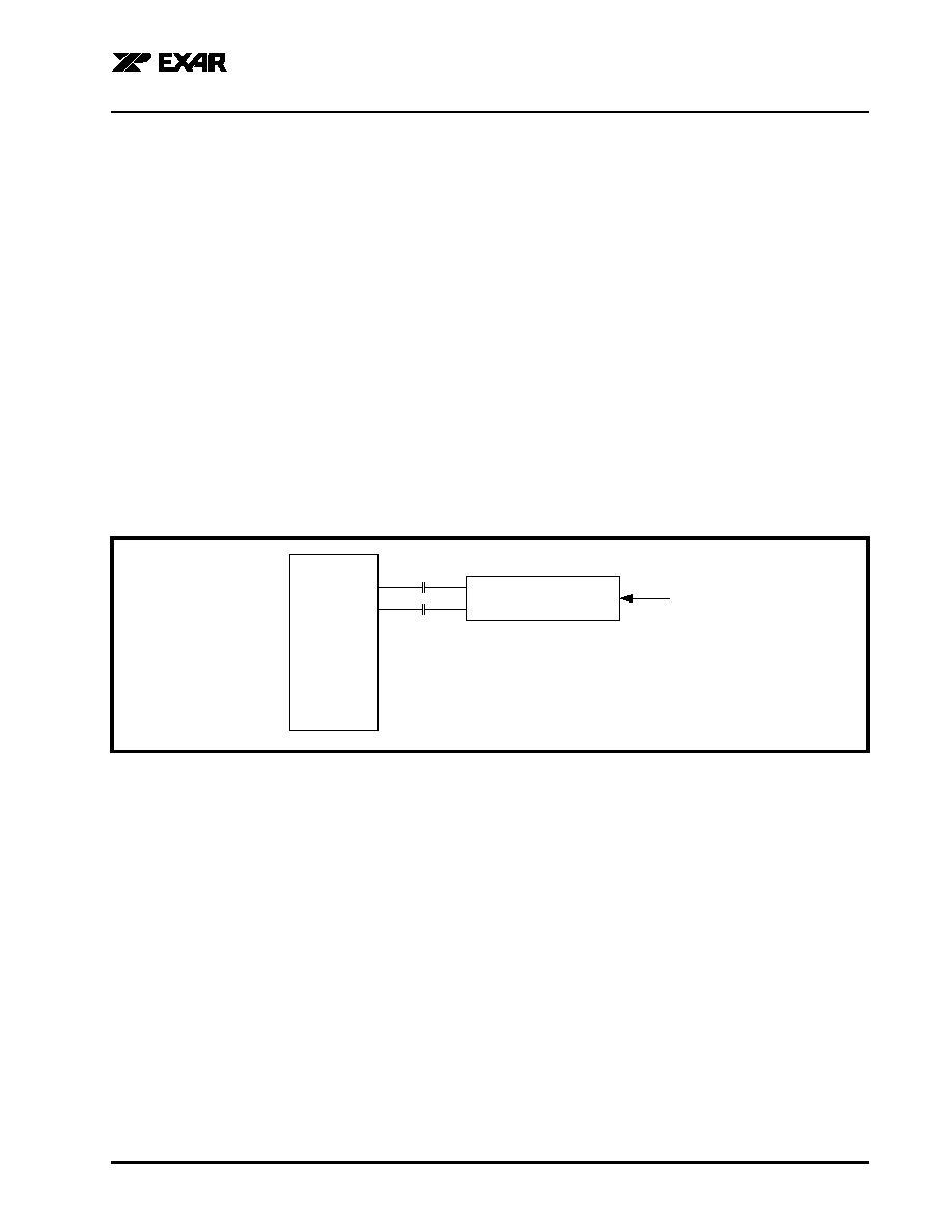
Receive Serial Input
The receive serial inputs can be applied to either the primary or secondary inputs selected by RXSEL. If
RXSEL is pulled "Low", the primary channel RXI0P/N is active. If RXSEL is pulled "High", the secondary
channel RXI1P/N is active. The receive serial inputs should be AC coupled to an optical module or an
electrical interface. A simplified block diagram is shown in Figure 3.
N
OTE
: Some optical modules integrate AC coupled capacitors within the module. If so, the external AC coupled capacitors
are not necessary and can be excluded.
F
IGURE
3. R
ECEIVE
S
ERIAL
I
NPUT
I
NTERFACE
B
LOCK
OC-48
Transceiver
Optical Module
0.1
�
F
0.1
�
F
RXI0P
RXI0N
XRT91L81
2.488/2.666GBPS OC-48/STM-16 SONET/SDH TRANSCEIVER
REV. P1.0.3
PRELIMINARY
14
2.2
Receive Clock and Data Recovery
The clock and data recovery unit accepts the high speed NRZ serial data from the differential CML receiver
and generates a clock that is the same frequency as the incoming data. The clock recovery utilizes the
REFCLKP/N to train and monitor its clock recovery PLL. Initially upon startup, the PLL locks to the reference
clock. Once this is achieved, the PLL then attempts to lock onto the incoming receive data stream. Whenever
the recovered clock frequency deviates from the local reference clock frequency by more than approximately
500 ppm, the clock recovery PLL will switch and lock back onto the local reference clock. When this condition
occurs the PLL will declare Loss of Lock and the LOCKDET_CDR signal will be pulled low. A Loss of Lock
condition will also be declared when the external LOSEXT is asserted. Whenever a loss of lock/loss of signal
event occurs, the CDR will continue to supply a receive clock (based on the local reference) to the upstream
framer device. When the DISRD control is enabled, receive parallel output data will be forced to an all zeroes
condition for the entire duration that a LOS condition is detected. This acts as a receive data mute upon LOS
function to prevent random noise from being misinterpreted as valid incoming data. When the LOSEXT
becomes inactive and the recovered clock is determined to be within 500 ppm accuracy with respect to the
local reference source, the lock detect output (LOCKDET_CDR) will go active.
2.3
Loss Of Signal
XRT91L81 supports external loss of signal detection (LOS). The external LOS function is supported by the
LOSEXT input. The TTL input is coming from the optical module through an output usually called "SD" or
"FLAG" which indicates the lack or presence of optical power. Depending on the manufacturer of these devices
the polarity of this signal can be either active low or active high. The LOSEXT and POLARITY inputs are
Exclusive NORed to generate the external loss control signal with the correct polarity. Whenever an external
LOS is detected, the XRT91L81 will automatically output a high level signal on the LOSDET output pin as well
as update the control registers whenever the host mode serial microprocessor interface feature is active.
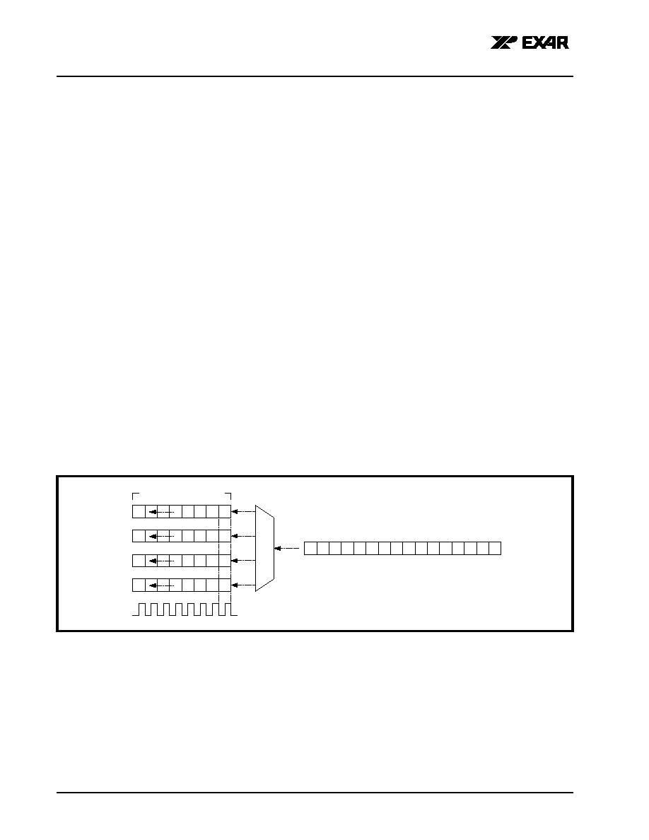
2.4
Receive Serial Input to Parallel Output (SIPO)
The SIPO is used to convert the 2.488/2.666GHz serial input data to 622/666MHz parallel output data which
can interface to a SONET Framer/ASIC. The SIPO bit de-interleaves the serial input data into a 4-bit parallel
output to RXD3P/N. A simplified block diagram is shown in Figure 4.
F
IGURE
4. S
IMPLIFIED
B
LOCK
D
IAGRAM
OF
SIPO
b
0
0
b
0
1
b
0
2
b
0
3
b
1
0
b
1
1
b
1
2
b
1
3
b
2
0
b
2
1
b
2
2
b
2
3
b
3
0
b
3
1
b
3
2
b
3
3
4-bit Parallel LVDS Output Data
RXD0P/N
RXD3P/N
RXD2P/N
RXD1P/N
RXI0P/N
RXCLKP/N
622MHz
b
3
0 b
2
0 b
1
0 b
0
0
b
3
1 b
2
1 b
1
1 b
0
1
b
3
2 b
2
2 b
1
2 b
0
2
b
0
3
b
1
3
b
2
3
b
3
3
2.488GHz
SI
PO
XRT91L81
2.488/2.666GBPS OC-48/STM-16 SONET/SDH TRANSCEIVER
PRELIMINARY
REV. P1.0.3
15
2.5
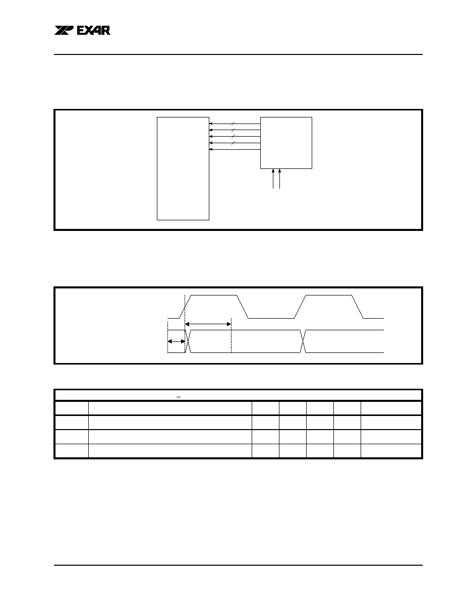
Receive Parallel Output Interface
The 4-bit LVDS 622/666MHz parallel output data of the receive path is used to interface to a SONET Framer/
ASIC synchronized to the recovered clock. A simplified block diagram is shown in Figure X.
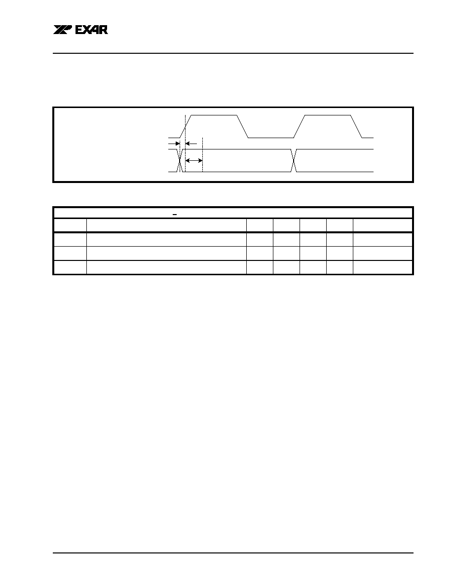
2.6
Receive Parallel Output Data Timing
The receive parallel output data from the OC-48 receiver will adhere to the setup and hold times shown in
Figure 6 and Table 3.
F
IGURE
6. R
ECEIVE
P
ARALLEL
O
UTPUT
T
IMING
T
ABLE
3: R
ECEIVE
P
ARALLEL
O
UTPUT
D
ATA
T
IMING
S
PECIFICATIONS
2.7
Disable Receive Output Data Upon LOS
The Receiver outputs can automatically be pulled "Low" during a LOS condition to prevent data chattering. By
pulling DISRD "High", the Receiver outputs will pull "Low" any time a LOS condition occurs.
2.8
Tri-State Receive Output Data
Unlike DISRD, TRIRXD is used to tri-state the Receiver outputs regardless of the input data stream. By pulling
TRIRXD "High", the Receiver outputs will automically tri-state.
F
IGURE
5. R
ECEIVE
P
ARALLEL
O
UTPUT
I
NTERFACE
B
LOCK
Test Conditions: TA = 25�C, VDD = 3.3V + 5% unless otherwise specified
S
YMBOL
P
ARAMETER
M
IN
.
T
YP
.
M
AX
.
U
NITS
C
ONDITIONS
RX
INV
RxCLKP/N "High" to data invalid window
200
pS
RX
DEL
RxCLKP/N "High" to data delay
45
55
%
RX
DTY
RxCLKP/N Duty Cycle
50
%
SONET Framer/ASIC
XRT91L81 OC48
Transceiver
RXDO0P/N
RXDO1P/N
RXDO3P/N
RXDO2P/N
RXCLKP/N
DI
SR
D
TRIR
XD
RX
INV
RX
DEL
RxCLKP/N
RxDO[3:0]P/N
XRT91L81
2.488/2.666GBPS OC-48/STM-16 SONET/SDH TRANSCEIVER
REV. P1.0.3
PRELIMINARY
16
3.0
TRANSMIT SECTION
The transmit section of the XRT91L81 accepts 4-bit parallel LVDS data and converts it to serial CML output
data intented to interface to an optical module. It consists of a 4-bit parallel LVDS interface, a 4x9 FIFO,
Parallel-to-Serial Converter, a clock multiplier unit (CMU), a Current Mode Logic (CML) differential line driver,
and Loop Timing modes. The CML serial output data rate is 2.488/2.666Gbps for OC-48 applications. The high
frequency serial clock is synthesized by a PLL, which uses a low frequency clock as its input reference. In
order to synchronize the data transfer process, the synthesized 2.488/2.666GHz serial output clock is divided
by four and the 622/666MHz clock is presented to the upstream device to be used as its timing source.
3.1
Transmit Parallel Interface
The parallel data from an upstream device is presented to the XRT91L81 through a 4-bit LVDS parallel bus
interface TXDI[3:0]. The data is latched into a parallel input register on the rising edge of TXPCLKIP/N. If the
SONET Framer/ASIC is synchronized to the same timing source as the XRT91L81, the transmit input data and
clock can directly interface to the OC-48 transceiver. However, if the SONET Framer/ASIC is synchronized to
a separate crystal, the XRT91L81 has two output clock references that can be used to synchronize the SONET
Framer/ASIC. TXPCLKOP/N is a 622/666MHz LVDS output clock source that is derived from the input clock
reference of the transceiver. TXCLKO16P/N is a 155.52/166MHz LVDS auxillary output clock source that is
also derived from the input clock reference. Either of these two output clock sources can be used to
synchronize the SONET Framer/ASIC to the XRT91L81. If the auxillary clock source is not used, it can be tri-
stated by pulling TRIRXCLKO16 "High". A simplified block diagram of the parallel interface is shown in
Figure 7.
F
IGURE
7. T
RANSMIT
P
ARALLEL
I
NPUT
I
NTERFACE
B
LOCK
SONET Framer/ASIC
XRT91L81 OC48
Transceiver
TXDI0P/N
TXDI1P/N
TXDI3P/N
TXDI2P/N
TXCLKIP/N
TXPCLKOP/N
T
X
C
L
K
O
16P
/
N
T
R
I
R
X
C
LK
O
16P
/
N
XRT91L81
2.488/2.666GBPS OC-48/STM-16 SONET/SDH TRANSCEIVER
PRELIMINARY
REV. P1.0.3
17
3.2
Transmit Parallel Input Data Timing
When applying parallel input data to the transmitter, the setup and hold times should be followed as shown in
Figure 8 and Table 4.
F
IGURE
8. T
RANSMIT
P
ARALLEL
I
NPUT
T
IMING
T
ABLE
4: T
RANSMIT
P
ARALLEL
I
NPUT
D
ATA
T
IMING
S
PECIFICATIONS
3.3
Transmit FIFO
The Parallel Interface also includes a 4x9 FIFO that can be used to eliminate difficult timing issues between the
input transmit clock and the clock derived from the CMU. The use of the FIFO permits the system to tolerate an
arbitrary amount of delay and jitter between TXCLKOP/N and TXCLKIP/N. The FIFO can be initialized when
FIFO_RESET is asserted and held low for 10 cycles of the TXCLKO clock. Once the FIFO is centered, the
delay between TXCLKO and TXCLKI can decrease or increase up to two periods of the low-speed clock
(TXCLKO). Should the delay exceed this amount, the read and write pointers will point to the same word in the
FIFO resulting in a loss of transmitted data (FIFO overflow). In the event of a FIFO overflow the FIFO control
logic will initiate an OVERFLOW signal that can be used by an external controller to issue a RESET signal. The
chip under the control of the FIFO_AUTORST pin can automatically recover from an overflow condition. When
the FIFO_AUTORST input is set to a "High" level, once an overflow condition is detected, the chip will set the
OVERFLOW pin to a high level and will automatically reset and center the FIFO. For the transparent mode of
operation (no FIFO), the RESET should be held at a constant "High" state.
3.4
FIFO Calibration Upon Power Up
It is required that the FIFO_RST pin be pulled "High" for 10 TXCLK cycles to flush out the FIFO after the device
is powered on. If the FIFO experiences an Overflow condition, FIFO_RST can be used to manually reset the
FIFO. However, the OC-48 transceiver has an automatic reset pin that will allow the FIFO to automatically
reset upon an Overflow condition. FIFO_AUTORST should be pulled "High" to enable the automatic FIFO
reset function.
Test Conditions: TA = 25�C, VDD = 3.3V + 5% unless otherwise specified
S
YMBOL
P
ARAMETER
M
IN
.
T
YP
.
M
AX
.
U
NITS
C
ONDITIONS
TX
TS
TxCLKIP/N "High" to data setup time
300
pS
TX
TH
TxCLKIP/N "High" to data hold time
300
pS
TX
DTY
TxCLKIP/N Duty Cycle
40
60
%
TX
TS
TX
TH
TxCLKIP/N
TxDI[3:0]P/N
XRT91L81
2.488/2.666GBPS OC-48/STM-16 SONET/SDH TRANSCEIVER
REV. P1.0.3
PRELIMINARY
18
3.5
Transmit Parallel Input to Serial Output (PISO)
The PISO is used to convert 622/666MHz parallel input data to 2.488/2.666GHz serial output data which can
interface to an optical module. The PISO bit interleaves parallel input data into a serial bit stream taking the
first bit from TXDI3P/N, then the first bit from TXDI2P/N, and so on as shown in Figure 9.
3.6
Clock Multiplier Unit (CMU) and Re-Timer
The high-speed serial clock synthesized by the CMU is divided by 4, and the TXPCLKOP/N clock is presented
to an upstream device. The upstream device should use TXPCLKOP/N as its timing source. The Upstream
device then generates the TXCLKIP/N clock that is phase aligned with the transmit data and provides it to the
parallel interface of the transmitter. The data must meet setup and hold times with respect to TXCLKIP/N. The
XRT91L81 will latch TXDI[3:0]P/N on the falling edge of TXCLKIP/N. The clock synthesizer uses a PLL to lock
to the differential input reference clock. It can also be driven by an optional external VCXO for loop timed or
local reference de-jitter applications. As an example the REFCLKP/N input can accept a clock from a LVPECL
crystal oscillator that has a frequency accuracy better than 20ppm in order for the TXCLKOP/N frequency to
have the accuracy required for SONET systems. The other input, VCXO_INP/N can be connected to the
output of a VCXO that can be configured to clean up the recovered received clock in loop timing mode before
being applied to the input of the transmit CMU as a reference clock. In addition, the internal phase/frequency
detector and charge pump, combined with an external VCXO can alternately be used as a jitter attenuator to
de-jitter a noisy system reference clock prior to it being used to time the CMU. Figure 10 provides a detailed
overview of the transmit FIFO in a system interface.
F
IGURE
9. S
IMPLIFIED
B
LOCK
D
IAGRAM
OF
PISO
b
0
0
b
0
1
b
0
2
b
0
3
b
0
4
b
0
5
b
0
6
b
0
7
b
1
0
b
1
1
b
1
2
b
1
3
b
1
4
b
1
5
b
1
6
b
1
7
b
2
0
b
2
1
b
2
2
b
2
3
b
2
4
b
2
5
b
2
6
b
2
7
b
3
0
b
3
1
b
3
2
b
3
3
b
3
4
b
3
5
b
3
6
b
3
7
4-bit Parallel LVDS Input Data
TXDI0P/N
TXDI3P/N
TXDI2P/N
TXDI1P/N
TXOP/N
TXCLKIP/N
622MHz
2.488GHz
b
0
0
b
1
0
b
2
0
b
3
0
b
0
1
b
1
1
b
2
1
b
3
1
b
0
2
b
1
2
b
2
2
b
3
2
b
0
3
b
1
3
b
2
3
b
3
3
PI
SO
time (0)
XRT91L81
2.488/2.666GBPS OC-48/STM-16 SONET/SDH TRANSCEIVER
PRELIMINARY
REV. P1.0.3
19
F
IGURE
10. T
RANSMIT
FIFO
AND
S
YSTEM
I
NTERFACE
Write Pointer
Read Pointer
TXDI[3:0]P/N
AUTORST
OVERFLOW
RESET
TXCLKIP/N
REFCLKP/N
FIFO Control
Div by 4
2.488/2.666GHz PLL
CMU
delay
Upstream Device
4 x 9 FIFO
4
4
XRT91L81
XRT91L81
2.488/2.666GBPS OC-48/STM-16 SONET/SDH TRANSCEIVER
REV. P1.0.3
PRELIMINARY
20
3.7
Loop Timing and clock control
Two types of loop timing are possible in the XRT91L81. In the regular loop timing mode (without an external
VCXO), the loop timing is controlled by the LPTIME_NO_JA pin. This mode is selected by asserting the
LPTIME_NO_JA signal to a high level. When the loop timing mode is activated the external reference clock to
the input of the CMU is replaced with the 1/16th or the 1/32nd of the high-speed recovered receive clock from
the CDR. Under this condition both the transmit and receive sections are synchronized to the recovered
receive clock. The normal looptime mode directly locks the CMU to the recovered receive clock with no
external de-jittering.
In cases when the jitter of the recovered receive clock does not satisfy the strict ITU and Bellcore jitter
generation requirements, an external VCXO-based PLL can be used to clean up the jitter of the recovered
receive clock. In this case the VCXO_SEL pin should be set high. By doing so, the CMU receives its reference
clock signal from an external VCXO connected to the VCXO_INP/N inputs. The LPTIME_JA pin must also be
set high in order to select the recovered receive clock as the reference source for the de-jitter PLL. In this state,
the VCXO will be phase locked to the recovered receive clock through a narrowband loop filter. The use of the
on-chip phase/frequency detector with charge pump and an external VCXO to remove the transmit jitter due to
jitter in the recovered clock is shown in Figure 10. The on-chip phase/frequency detector can also be used to
remove the jitter from a noisy reference signal that is applied to the REFCLKP/N inputs. In this case the
LPTIME_NO_JA pin should be set "Low", the VCXO_SEL set "High", and the LPTIME_JA pin set "Low". In this
configuration, the REFCLKP/N signal is used as the reference to the de-jitter PLL and the de-jittered output of
the phase locked VCXO is used as the timing reference to the CMU. Table 5 provides configuration for
selecting the loop timing and reference de-jitter modes.
T
ABLE
5: L
OOP
TIMING
AND
REFERENCE
DE
-
JITTER
CONFIGURATIONS
VCXO_SEL
LPTIME_JA
LPTIME_NO_JA
A
CTION
0
0
0
Normal mode
0
0
1
Loop timing without de-jitter
1
0
0
Reference de-jitter
1
1
0
Loop timing with de-jitter
XRT91L81
2.488/2.666GBPS OC-48/STM-16 SONET/SDH TRANSCEIVER
PRELIMINARY
REV. P1.0.3
21
3.8
External Loop Filter
As shown in Figure 11, there is an internal charge pump used to drive an external loop filter and external
VCXO. The charge pump current is fixed at 250uA. Figure 12 is a simplified block diagram of the external loop
filter and recommended values.
F
IGURE
12. S
IMPLIFIED
D
IAGRAM
OF
THE
E
XTERNAL
L
OOP
F
ILTER
F
IGURE
11. L
OOP
T
IMING
M
ODE
U
SING
AN
E
XTERNAL
C
LEANUP
VCXO
CPOUT
LPTIME_JA
RXIP
RXIN
Charge
Pump
MU
X
Phase
Detect
CDR
MU
X
MU
X
MU
X
Loop Filter
2.488/2.666GHz
CMU
VCXO_SEL
REFCLK0P
REFCLK0N
LPTIME_NO_JA
LOCKDET_CMU
REFFREQSEL
VCXO_INP
VCXO_INN
Div by 4
Div by 4
Clk
Data
a
a
a
a
VCXO
XRT91L81
XRT91L81
2.488/2.666GBPS OC-48/STM-16 SONET/SDH TRANSCEIVER
REV. P1.0.3
PRELIMINARY
22
3.9
Transmit Serial Output Control
The 2.488/2.666GHz transmit serial output has a primary and secondary channel. By default, the serial output
stream is multiplexed to both channels. However, the secondary channel can be configured to output the
2.488/2.666GHz serial data stream or the transmit serial clock according to the state of TXO2_SEL. If
TXO2_SEL is pulled "Low", the secondary channel will output the serial data stream. If TXO2_SEL is pulled
"High", the secondary channel will output the transmit serial clock. In addition, the secondary channel can be
disabled by pulling TXO2_DIS "High". If the secondary channel is disabled, the secondary serial output data
will be pulled "High". The transmit serial output should be AC coupled to an optical module or electrical
interface. A simplified block diagram is shown in Figure 13.
N
OTE
: Some optical modules integrate AC coupled capacitors within the module. If so, the external AC coupled capacitors
are not necessary and can be excluded.
F
IGURE
13. T
RANSMIT
S
ERIAL
O
UTPUT
I
NTERFACE
OC-48
Transceiver
Optical Module
0.1
�
F
0.1
�
F
TXOP
TXON
XRT91L81
2.488/2.666GBPS OC-48/STM-16 SONET/SDH TRANSCEIVER
PRELIMINARY
REV. P1.0.3
23
4.0
DIAGNOSTIC FEATURES
4.1
Serial Remote Loopback
The serial remote loopback function is activated by setting RLOOPS "High". When serial remote loopback is
activated, the high-speed serial receive data from RXIN is presented at the high speed transmit output TXOP/
N, and the high-speed recovered clock is selected and presented to the high-speed transmit clock output
TXCLKP/N. During serial remote loopback, the high-speed receive data (RXIN) is also converted to parallel
data and presented at the low-speed receive parallel interface RXD[3:0]P/N. The recovered receive clock is
also divided by 4 and presented at the low-speed clock output RXCLKP/N to synchronize the transfer of the 4-
bit received parallel data. A simplified block diagram of serial remote loopback is shown in Figure 14.
4.2
Parallel Remote Loopback
RLOOPP controls a more comprehensive version of remote loop-back that can also be used in conjunction
with the de-jitter PLL that is phase locked to the recovered receive clock. In this mode, the received signal
traverses the limiting amplifier, is processed by the CDR, and is sent through the serial to parallel converter. At
this point, the 4-bit parallel data and clock are looped back to the transmit FIFO. Concurrently, if receive clock
jitter attenuation is also employed, the received clock is divided down in frequency and presented to the input
of the integrated phase/frequency detector and is compared to the frequency of a VCXO that is connected to
the VCXO_INP/N inputs. With the LOOPTIME configured to use the recovered receive clock as the reference
and VCXO_SEL asserted, the VCXO is phase locked to the recovered receive clock. The de-jittered clock is
then used to retime the transmitter, resulting in the re-transmission of the de-jittered received data out of
TXOP/N. A simplified block diagram of parallel remote loopback is shown in Figure 15.
F
IGURE
14. S
ERIAL
R
EMOTE
L
OOPBACK
F
IGURE
15. P
ARALLEL
R
EMOTE
L
OOPBACK
PISO
Re-Timer
Output Drivers
FIFO
SIPO
CDR
Input MUX
Serial Remote Loopback
Rx Parallel Output
Tx Serial Output
Rx Serial Input
PISO
Re-Timer
Output Drivers
FIFO
SIPO
CDR
Input MUX
Parallel Remote Loopback
Rx Parallel Output
Tx Serial Output
Rx Serial Input
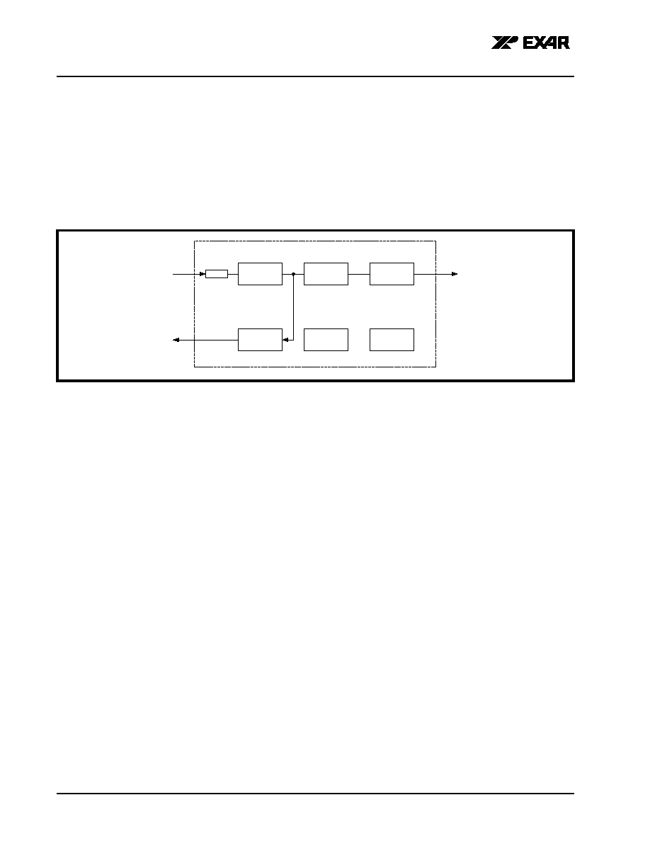
XRT91L81
2.488/2.666GBPS OC-48/STM-16 SONET/SDH TRANSCEIVER
REV. P1.0.3
PRELIMINARY
24
4.3
Digital Local Loopback
The digital local loopback is activated when the DLOOP signal is set high. When digital local loopback is
activated, the high-speed data from the output of the parallel to serial converter is looped back and presented
to the high-speed input of the receiver serial to parallel converter. The CMU output is also looped back to the
receive section and is used to synchronize the transfer of the data through the receiver. In Digital loopback
mode the transmit data from the transmit parallel interface TXDI[3:0]P/N is serialized and presented to the
high-speed transmit output TXOP/N along with the high-speed transmit clock which is generated from the clock
multiplier unit and presented to the TXO2P/N pins. A simplified block diagram of digital loopback is shown in
Figure 16.
F
IGURE
16. D
IGITAL
L
OOPBACK
PISO
Re-Timer
Output Drivers
FIFO
SIPO
CDR
Input MUX
Digital Loopback
Tx Parallel Input
Rx Parallel Output
Tx Serial Output
XRT91L81
2.488/2.666GBPS OC-48/STM-16 SONET/SDH TRANSCEIVER
PRELIMINARY
REV. P1.0.3
25
4.4
SONET Jitter Requirements
SONET equipment jitter requirements are specified for the following three types of jitter. The definitions of each
of these types of jitter are given below. SONET equipment jitter requirements are specified for the following
three types of jitter.
4.4.1
Jitter Tolerance:
Jitter tolerance is defined as the peak-to-peak amplitude of sinusoidal jitter applied on the input OC-N
equipment interface that causes an equivalent 1dB optical power penalty. OC-1/STS-1, OC-3/STS-3, OC-12
and OC-48 category II SONET interfaces should tolerate, the input jitter applied according to the mask of
Figure 17, with the corresponding parameters specified in the figure.
F
IGURE
17. J
ITTER
T
OLERANCE
M
ASK
OC-N/STS-N LE VEL
1
3
12
48
F0 (HZ)
10
10
10
10
F1 (HZ)
30
30
30
600
F2 (HZ)
300
300
300
6000
F3 (HZ)
2K
6.5K
25K
100K
F4 (HZ)
20K
65K
250K
1000K
A1 (UIP P)
0.15
0.15
0.15
0.15
A2 (UIPP)
1.5
1.5
1.5
1.5
A3 (UIP P)
15
15
15
15
Input
Jitter
Am plitude
(UI
pp
)
A
3
A
2
A
1
f
0
f
1
f
2
f
3
f
4
slope= -20dB/decade
slope= -20dB/decade
Jitter Frequency (Hz)

XRT91L81
2.488/2.666GBPS OC-48/STM-16 SONET/SDH TRANSCEIVER
REV. P1.0.3
PRELIMINARY
26
4.4.2
Jitter Transfer
Jitter transfer is defined as the ratio of the jitter on the output of OC-N to the jitter applied on the input of OC-N
versus frequency. Jitter transfer is important in applications where the system is utilized in the loop-timed
mode, where the recovered clock is used as the source of the transmit clock.
4.4.3
Jitter Generation
Jitter generation is defined as the amount of jitter at the OC-N output in the absence of applied input jitter. The
Bellcore and ITU requirement for this type jitter is 0.01UI rms measured with a specific band-pass filter.
For more information on these specifications refer to Bellcore TR-NWT-000253 sections 5.6.2-5 and GR-253-
CORE section 5.6.
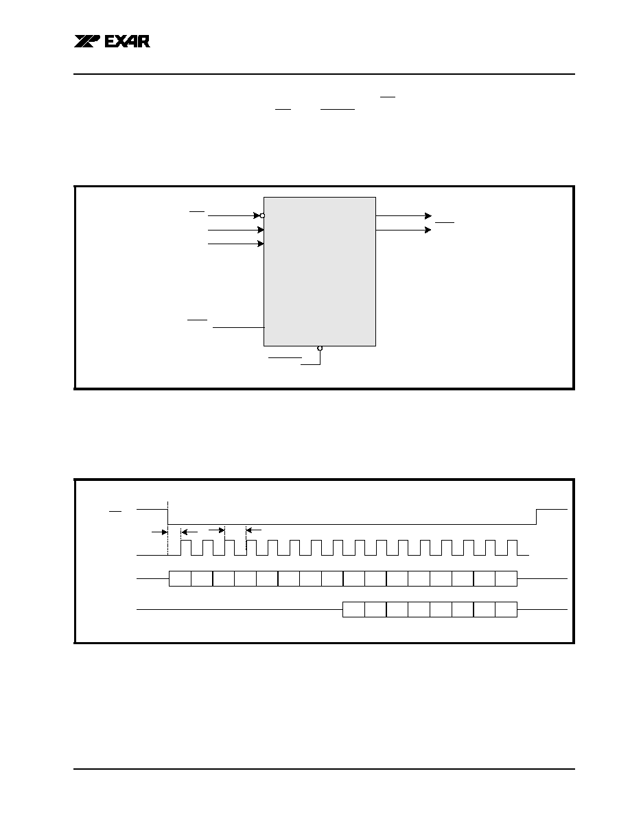
XRT91L81
2.488/2.666GBPS OC-48/STM-16 SONET/SDH TRANSCEIVER
PRELIMINARY
REV. P1.0.3
27
5.0
SERIAL MICROPROCESSOR INTERFACE BLOCK
The serial microprocessor uses a standard 3-pin serial port with CS, SCLK, and SDI for programming the
transceiver. Optional pins such as SDO, INT, and RESET allow the ability to read back contents of the
registers, monitor the transceiver via an interrupt pin, and reset the transceiver to its default configuration by
pulling reset "Low" for more than 10mS. A simplified block diagram of the Serial Microprocessor is shown in
Figure 18.
F
IGURE
18. S
IMPLIFIED
B
LOCK
D
IAGRAM
OF
THE
S
ERIAL
M
ICROPROCESSOR
I
NTERFACE
5.1
S
ERIAL
T
IMING
I
NFORMATION
The serial port requires 16 bits of data applied to the SDI (Serial Data Input) pin. The Serial Microprocessor
samples SDI on the rising edge of SCLK (Serial Clock Input). The data is not latched into the device until all 16
bits of serial data have been sampled. A timing diagram of the Serial Microprocessor is shown in Figure 19.
F
IGURE
19. T
IMING
D
IAGRAM
FOR
THE
S
ERIAL
M
ICROPROCESSOR
I
NTERFACE
Serial
Microprocessor
Interface
CS
SDI
SCLK
SDO
RESET
INT
HW/Host
CS
SDI
SCLK
SDO
1
2
10
9
8
7
6
5
4
3
11
16
15
13
14
12
R/W
A0
A1
A2
A3
A4
A5
X
D0
D1
D7
D6
D5
D4
D3
D2
D0
D1
D7
D6
D5
D4
D3
D2
High-Z
High-Z
25nS
50nS

XRT91L81
2.488/2.666GBPS OC-48/STM-16 SONET/SDH TRANSCEIVER
REV. P1.0.3
PRELIMINARY
28
5.2
16-B
IT
S
ERIAL
D
ATA
I
NPUT
D
ESCRITPTION
The serial data input is sampled on the rising edge of SCLK. In readback mode, the serial data output is
updated on the falling edge of SCLK. The serial data must be applied to the transceiver LSB first. The 16 bits
of serial data are described below.
5.2.1
R/W (SCLK1)
The first serial bit applied to the transceiver informs the microprocessor that a Read or Write operation is
desired. If the R/W bit is set to "0", the microprocessor is configured for a Write operation. If the R/W bit is set
to "1", the microprocessor is configured for a Read operation.
5.2.2
A[5:0] (SCLK2 - SCLK7)
The next 6 SCLK cycles are used to provide the address to which a Read or Write operation will occur. A0
(LSB) must be sent to the transceiver first followed by A1 and so forth until all 6 address bits have been
sampled by SCLK.
5.2.3
X (Dummy Bit SCLK8)
The dummy bit sampled by SCLK8 is used to allow sufficient time for the serial data output pin to update data if
the readback mode is selected by setting R/W = "1". Therefore, the state of this bit is ignored and can hold
either "0" or "1" during both Read and Write operations.
5.2.4
D[7:0] (SCLK9 - SCLK16)
The next 8 SCLK cycles are used to provide the data to be written into the internal register chosen by the ad-
dress bits. D0 (LSB) must be sent to the transceiver first followed by D1 and so forth until all 8 data bits have
been sampled by SCLK. Once 16 SCLK cycles have been complete, the transceiver holds the data until CS is
pulled "High" whereby, the serial microprocessor latches the data into the selected internal register.
5.3
8-B
IT
S
ERIAL
D
ATA
O
UTPUT
D
ESCRIPTION
The serial data output is updated on the falling edge of SCLK9 - SCLK16 if R/W is set to "1". D0 (LSB) is pro-
vided on SCLK9 to the SDO pin first followed by D1 and so forth until all 8 data bits have been updated. The
SDO pin allows the user to read the contents stored in individual registers by providing the desired address on
the SDI pin during the Read cycle.
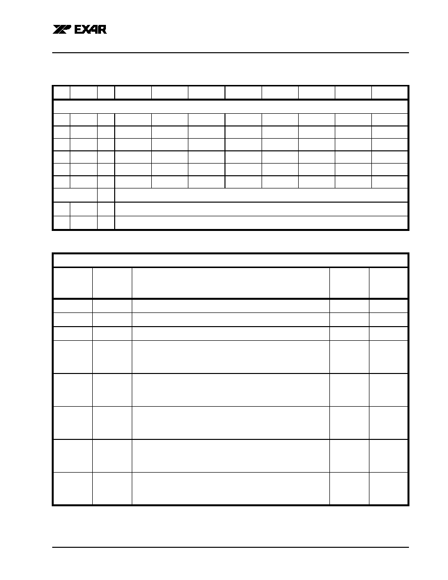
XRT91L81
2.488/2.666GBPS OC-48/STM-16 SONET/SDH TRANSCEIVER
PRELIMINARY
REV. P1.0.3
29
6.0
REGISTER MAP AND BIT DESCRIPTIONS
T
ABLE
7: M
ICROPROCESSOR
R
EGISTER
B
IT
D
ESCRIPTION
T
ABLE
6: M
ICROPROCESSOR
R
EGISTER
M
AP
R
EG
ADDR T
YPE
D7
D6
D5
D4
D3
D2
D1
D0
Channel 0 Control Register (0x00h - 0x05h)
0
0x00
R/W
Reserved
Reserved
Reserved
VCXOIE
LOSIE
CDRIE
CMUIE
FIFOIE
1
0x01
RUR
Reserved
Reserved
Reserved
VCXOIS
LOSIS
CDRIS
CMUIS
FIFOIS
2
0x02
RO
Reserved
Reserved
Reserved
VCXOID
LOSID
CDRID
CMUID
FIFOID
3
0x03
R/W
TXO2DIS
REFREQSEL
TXO2SEL
LOOPBW
VCXOSEL
TRITXCLK016
AUTORST
FIFORST
4
0x04
R/W
Reserved
POLARITY
LOOPTM
LPTIMJADIS
DISRD
TRIRXD
RXSEL
VCXOLKEN
5
0x05
R/W
Reserved
Reserved
Reserved
Reserved
Reserved
DLOOP
RLOOPS
RLOOPP
0x06 - 0x3D
R/W
Reserved
62
0x3E
RO
Device ID (See Bit Description)
63
0x3F
RO
Revision ID (See Bit Description)
C
HANNEL
0 C
ONTROL
R
EGISTER
(0
X
00
H
)
B
IT
N
AME
F
UNCTION
Register
Type
Default
Value
(HW reset)
D7
Reserved
This Register Bit is Not Used
X
X
D6
Reserved
This Register Bit is Not Used
X
X
D5
Reserved
This Register Bit is Not Used
X
X
D4
VCXOIE
Voltage Controlled External OscillatorLock Interrupt Enable
"0" = Masks the VCXO interrupt generation
"1" = Enables Interrupt generation
R/W
0
D3
LOSIE
Loss of Signal Interrupt Enable
"0" = Masks the LOS interrupt generation
"1" = Enables Interrupt generation
R/W
0
D2
CDRIE
Clock and Data Recovery Lock Interrupt Enable
"0" = Masks the CDR lock interrupt generation
"1" = Enables Interrupt generation
R/W
0
D1
CMUIE
Clock Multiplier Unit Lock Interrupt Enable
"0" = Masks the CMU lock interrupt generation
"1" = Enables Interrupt generation
R/W
0
D0
FIFOIE
FIFO Overflow Interrupt Enable
"0" = Masks the FIFO interrupt generation
"1" = Enables Interrupt generation
R/W
0

XRT91L81
2.488/2.666GBPS OC-48/STM-16 SONET/SDH TRANSCEIVER
REV. P1.0.3
PRELIMINARY
30
T
ABLE
9: M
ICROPROCESSOR
R
EGISTER
B
IT
D
ESCRIPTION
T
ABLE
8: M
ICROPROCESSOR
R
EGISTER
B
IT
D
ESCRIPTION
C
HANNEL
0 C
ONTROL
R
EGISTER
(0
X
01
H
)
B
IT
N
AME
F
UNCTION
Register
Type
Default
Value
(HW reset)
D7
Reserved
This Register Bit is Not Used
X
X
D6
Reserved
This Register Bit is Not Used
X
X
D5
Reserved
This Register Bit is Not Used
X
X
D4
VCXOIS
Voltage Controlled External Oscillator Lock Interrupt Status
"0" = No Change
"1" = Change in Status Occured
RUR
0
D3
LOSIS
Loss of Signal Interrupt Status
"0" = No Change
"1" = Change in Status Occured
RUR
0
D2
CDRIS
Clock and Data Recovery Lock Interrupt Status
"0" = No Change
"1" = Change in Status Occured
RUR
0
D1
CMUIS
Clock Multiplier Unit Lock Interrupt Status
"0" = No Change
"1" = Change in Status Occured
RUR
0
D0
FIFOIS
FIFO Overflow Interrupt Status
"0" = No Change
"1" = Change in Status Occured
RUR
0
C
HANNEL
0 C
ONTROL
R
EGISTER
(0
X
02
H
)
B
IT
N
AME
F
UNCTION
Register
Type
Default
Value
(HW reset)
D7
Reserved
This Register Bit is Not Used
X
X
D6
Reserved
This Register Bit is Not Used
X
X
D5
Reserved
This Register Bit is Not Used
X
X
D4
VCXOID
Voltage Controlled External Oscillator Lock Detection
The VCXOID is used to indicate whether the internal clock refer-
ence is locked to an external VCO. An interrupt will not occur
unless the VCXOIE is set to "1" in the channel register 0x00h.
"0" = No Alarm
"1" = No lock has occured for VCXO
RO
0

XRT91L81
2.488/2.666GBPS OC-48/STM-16 SONET/SDH TRANSCEIVER
PRELIMINARY
REV. P1.0.3
31
D3
LOSID
Loss of Signal Detection
The LOSID indicates the LOS activity. An interrupt will not occur
unless the RLOSIE is set to "1" in the channel register 0x00h.
"0" = No Alarm
"1" = A LOS condition is present
RO
0
D2
CDRID
Clock and Data Recovery Lock Detection
The CDRID is used to indicate that the CDR is locked. An interrupt
will not occur unless the CDRIE is set to "1" in the channel register
0x00h.
"0" = No Alarm
"1" = A LOS condition is present
RO
0
D1
CMUID
Clock Multiplier Unit Lock Detection
The CMUID is used to indicate that the CMU is locked. An inter-
rupt will not occur unless the CMUIE is set to "1" in the channel
register 0x00h.
"0" = No Alarm
"1" = A LOS condition is present
RO
0
D0
FIFOID
FIFO Overflow Detection
The FIFOID indicates that the FIFO has experienced an overflow
condition. An interrupt will not occur unless the FIFOIE is set to "1"
in the channel register 0x00h.
"0" = No Alarm
"1" = A LOS condition is present
RO
0
T
ABLE
10: M
ICROPROCESSOR
R
EGISTER
B
IT
D
ESCRIPTION
C
HANNEL
0 C
ONTROL
R
EGISTER
(0
X
03
H
)
B
IT
N
AME
F
UNCTION
Register
Type
Default
Value
(HW reset)
D7
TXO2DIS
Secondary Transmit Serial Output Disable
This bit is used to disable the secondary transmit serial output. By
default, the secondary transmit signal is enabled.
"0" = Enabled
"1" = Disabled
R/W
0
D6
REFREQSEL
Input Reference Frequency Select
This bit is used to select the input clock reference.
"0" = 77.76/83.3 MHz
"1"= 155.52/166 MHz
R/W
0
C
HANNEL
0 C
ONTROL
R
EGISTER
(0
X
02
H
)
B
IT
N
AME
F
UNCTION
Register
Type
Default
Value
(HW reset)

XRT91L81
2.488/2.666GBPS OC-48/STM-16 SONET/SDH TRANSCEIVER
REV. P1.0.3
PRELIMINARY
32
D5
TXO2SEL
Secondary Transmit Serial Output Select
This bit is used to select between serial data and a reference clock
for the secondary transmit serial output.
"0" = 2.488Gbit/s Serial Output Data
"1" = Transmit Output Clock (2.488/2.666 GHz)
R/W
0
D4
LOOPBW
CMU Loop Band Width Select
This bit is used to select the bandwidth of the clock multiplier unit
of the transmit path to a narrow or wide band.
"0" = Narrow Band (1x)
"1" = Wide Band (4x)
R/W
0
D3
VCXOSEL
VCXO De-Jitter Select
This bit selects either the normal REFCLK or the de-jitter VCXO as
a reference clock.
"0" = Normal REFCLK Mode
"1" = De-Jitter VCXO Mode
R/W
0
D2
TRITXCLKO16
Auxillary Output Clock Tri-State
This bit is used to tri-state the auxillary clock.
"0" = TXCLKO16 Enabled
"1" = TXCLKO16 Tri-State
R/W
0
D1
AUTORST
Automatic FIFO Overflow Reset
If this bit is set to "1", the OC-48 transceiver will automatically flush
the FIFO upon an overflow condition. Upon power-up, the FIFO
should be manually reset by setting FIFO_RST to "1" for 10 cycles
of TXCLK.
"0" = Manual FIFO reset required for overflow conditions
"1" = Automatically resets FIFO upon overflow detection
R/W
0
D0
FIFORST
Manual FIFO Reset
FIFORST should be set to "1" for 10 cycles of TXCLK during
power-up in order to flush out the FIFO. Upon an interrupt indica-
tion that the FIFO has an overflow condition, this bit is used to
reset or flush out the FIFO.
N
OTE
: To automaically reset the FIFO, see the AUTORST bit.
R/W
0
T
ABLE
10: M
ICROPROCESSOR
R
EGISTER
B
IT
D
ESCRIPTION
C
HANNEL
0 C
ONTROL
R
EGISTER
(0
X
03
H
)
B
IT
N
AME
F
UNCTION
Register
Type
Default
Value
(HW reset)

XRT91L81
2.488/2.666GBPS OC-48/STM-16 SONET/SDH TRANSCEIVER
PRELIMINARY
REV. P1.0.3
33
T
ABLE
11: M
ICROPROCESSOR
R
EGISTER
B
IT
D
ESCRIPTION
C
HANNEL
0 C
ONTROL
R
EGISTER
(0
X
04
H
)
B
IT
N
AME
F
UNCTION
Register
Type
Default
Value
(HW reset)
D7
Reserved
This Register Bit is Not Used
X
X
D6
POLARITY
Polarity for LOS Input Select
LOSEXT and POLARITY bits will be Exlussive NORed
internally to generate the correct polarity.
R/W
0
D5
LOOPTM_JA
Loop Timing With JA
The LOOPTM_JA bit must be set to "1" in order to select the recov-
ered receive clock as the reference source for the de-jitter PLL.
"0" = Disabled
"1" = Enabled
R/W
0
D4
LPTIMJADIS
Loop Timing With No JA
When the loop timing mode is activated the external reference
clock to the input of the CMU is replaced with the 1/16th or the 1/
32nd of the high-speed recovered receive clock from the CDR.
"0" = Disabled
"1" = Loop timing Activated
R/W
0
D3
DISRD
Receive Output Disable Upon LOS
If this bit is set to "1", the receive output data will automically pull
"Low" when a LOS condition occurs.
"0" = Disabled
"1" = Mute Data Upon LOS
R/W
0
D2
TRIRXD
Receive Output Tri-State
This bit is used to control the activity of the 4-bit parallel receive
output bus and its reference clock.
"0" = Normal Mode
"1" = Tri-State RXDP/N[3:0] and RXCLK
R/W
0
D1
RXSEL
Receive Serial Input Select
This bit is used to select the Receive Serial Data Input from the pri-
mary or secondary inputs.
"0" = RXI0
"1" = RXI1
R/W
0
D0
VCXOLKEN
De-Jitter PLL Lock Detect Enable
This bit enables the VCXO lock detect Pin N8 to be active.
"0" = VCXO_LOCK disabled
"1" = VCXO_LOCK enabled
R/W
0

XRT91L81
2.488/2.666GBPS OC-48/STM-16 SONET/SDH TRANSCEIVER
REV. P1.0.3
PRELIMINARY
34
T
ABLE
12: M
ICROPROCESSOR
R
EGISTER
B
IT
D
ESCRIPTION
C
HANNEL
0 C
ONTROL
R
EGISTER
(0
X
05
H
)
B
IT
N
AME
F
UNCTION
Register
Type
Default
Value
(HW reset)
D7
Reserved
This Register Bit is Not Used
X
X
D6
Reserved
This Register Bit is Not Used
X
X
D5
Reserved
This Register Bit is Not Used
X
X
D4
Reserved
This Register Bit is Not Used
X
X
D3
Reserved
This Register Bit is Not Used
X
X
D2
DLOOP
Digital Loopback
Digital loopback allows the Transmit input pins to be looped back
to the Receive output pins for local diagnostics. The Transmit
serial output data is valid during the digital loopback.
"0" = Disabled
"1" = Enable DLOOP
R/W
0
D1
RLOOPS
Serial Remote Loopback
Serial remote loopback allows the Receive serial input pins to be
looped back to the Transmit serial output pins for remote diagnos-
tics. The Receive output data is valid during a serial remote loop-
back.
"0" = Disabled
"1" = Enable RLOOPS
R/W
0
D0
RLOOPP
Parallel Remote Loopback
Parallel remote loopback has the same affect as the serial remote
loopback, except that the input data is allowed to pass through the
SIPO before it's looped back to the Transmit path, wherein it
passes through the Transmit FIFO, through the PISO, and back
out the Transmit serial output. The Receive output data is valid
during a serial remote loopback.
"0" = Disabled
"1" = Enable RLOOPP
R/W
0

XRT91L81
2.488/2.666GBPS OC-48/STM-16 SONET/SDH TRANSCEIVER
PRELIMINARY
REV. P1.0.3
35
T
ABLE
13: M
ICROPROCESSOR
R
EGISTER
0
X
02
H
B
IT
D
ESCRIPTION
T
ABLE
14: M
ICROPROCESSOR
R
EGISTER
0
X
01
H
B
IT
D
ESCRIPTION
D
EVICE
"ID" R
EGISTER
(0
X
3E
H
)
B
IT
N
AME
F
UNCTION
Register
Type
Default
Value
(HW reset)
D7
D6
D5
D4
D3
D2
D1
D0
Device "ID" The device "ID" of the XRT91L81 LIU is 0xC0h. Along with the
revision "ID", the device "ID" is used to enable software to identify
the silicon adding flexibility for system control and debug.
RO
1
1
0
0
0
0
0
0
R
EVISION
"ID" R
EGISTER
(0
X
3F
H
)
B
IT
N
AME
F
UNCTION
Register
Type
Default
Value
(HW reset)
D7
D6
D5
D4
D3
D2
D1
D0
Revision
"ID"
The revision "ID" of the XRT91L81 LIU is used to enable software
to identify which revision of silicon is currently being tested. The
revision "ID" for the first revision of silicon (Revision A) will be
0x01h.
RO
0
0
0
0
0
0
0
1
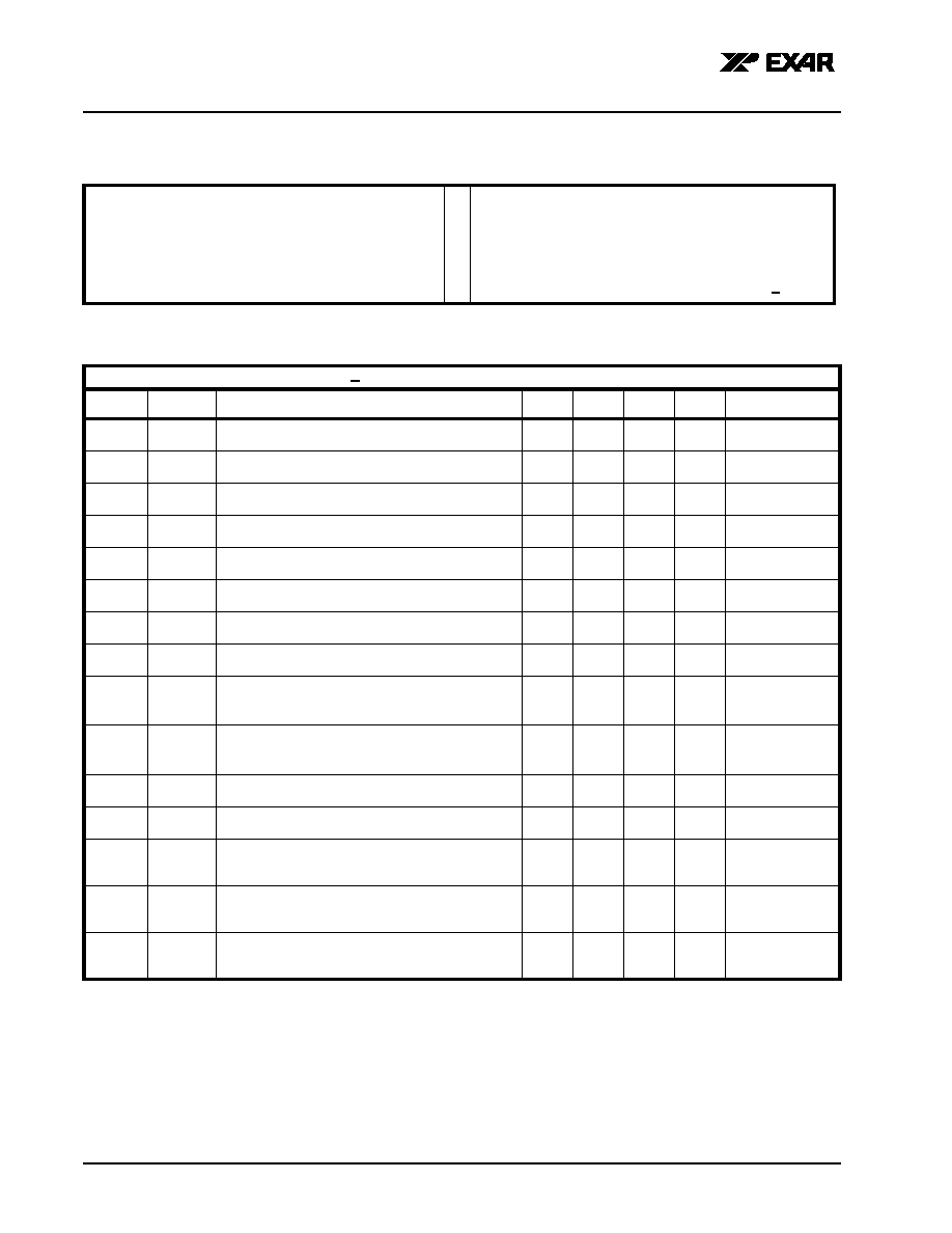
XRT91L81
2.488/2.666GBPS OC-48/STM-16 SONET/SDH TRANSCEIVER
REV. P1.0.3
PRELIMINARY
36
7.0
ELECTRICAL CHARACTERISTICS
ABSOLUTE MAXIMUMS
Power Supply......................................... -0.5V to +3.465V
Power Dissipation STBGA Package........................... TBD
Storage Temperature ...............................-65�C to 150�C
Input Logic Signal Voltage (Any Pin) .........-0.5V to + 5.5V
Operating Temperature Range.................-40�C to 85�C
ESD Protection (HBM)...........................................>2000V
Supply Voltage ...................... GND-0.5V to +VDD + 0.5V
Input Current (Any Pin) ...................................... + 100mA
DC ELECTRICAL CHARACTERISTICS
Test Conditions: TA = 25�C, VDD = 3.3V + 5% unless otherwise specified
S
YMBOL
T
YPE
P
ARAMETER
M
IN
.
T
YP
.
M
AX
.
U
NITS
C
ONDITIONS
I
DD
Power Supply Current
TBD
mA
I
LL
Data Bus Tri-State Bus Leakage Current
-10
+10
�A
V
HL
TTL
Input High Voltage
1.6
V
V
IL
TTL
Input Low Voltage
1.2
V
V
IDIFF
Analog
Input Differential Voltage
0.01
1
V
AC Coupled
V
COMM
Analog
Common Mode Voltage
1
2
V
V
ICOMM
LVDS
Input LVDS Common Mode Voltage
0.5
2
V
V
IAMP
LVDS
Input LVD Voltage
0.1
V
V
ICOMM
PECL
Input PECL Common Mode Voltage
1.5
2
V
Terminate with
50
to V
CC
-2
V
IAMP
PECL
Input PECL Voltage
0.2
V
Terminate with
50
to V
CC
-2
V
OH
TTL
Output High Voltage
2
V
V
OL
TTL
Output Low Voltage
0.8
V
V
OH
LVDS
Output LVDS High Voltage
1.35
V
Differential Ter-
mination, 100
V
OL
LVDS
Output LVDS Low Voltage
1.15
V
Differential Ter-
mination, 100
V
OAMP
CML
Output Common Mode Logic Voltage
0.4
0.6
V
AC Coupled,
50
to GND
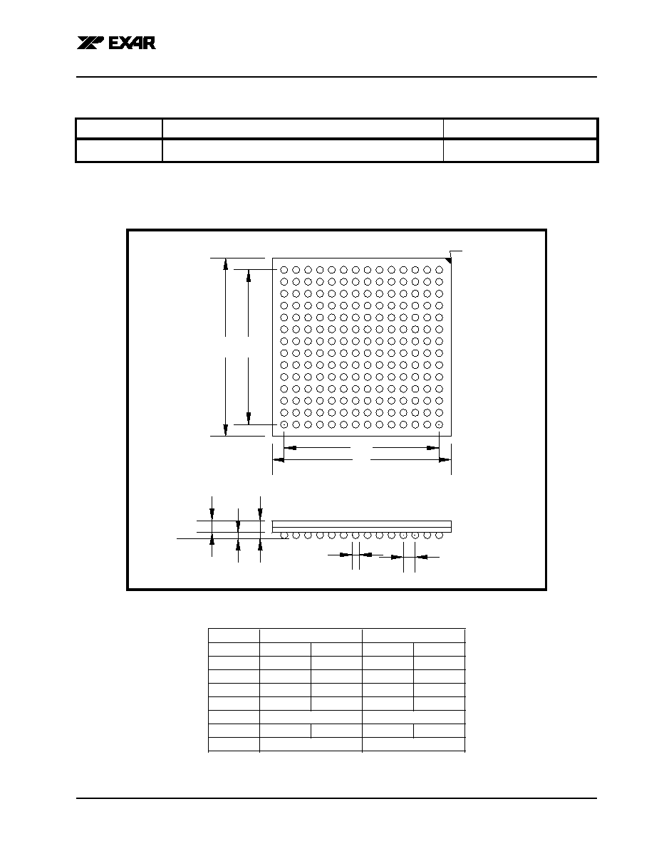
XRT91L81
2.488/2.666GBPS OC-48/STM-16 SONET/SDH TRANSCEIVER
PRELIMINARY
REV. P1.0.3
37
196 SHRINK THIN BALL GRID ARRAY
(12.0 MM X 12.0 MM, STBGA)
REV. 1.00
ORDERING INFORMATION
P
ART
N
UMBER
P
ACKAGE
O
PERATING
T
EMPERATURE
R
ANGE
XRT91L81IB
196 Shrink Thin Ball Grid Array (12.0 mm x 12.0 mm, STBGA)
-40
�
C to +85
�
C
(A1 corner feature is m fger option)
A
b
e
A1
A2
Seating
Plane
A
11 10
9
8
7
6
5
4
3
1
2
B
C
D
E
F
G
H
J
K
L
D
D1
A1 Feature/Mark
13
14
12
P
N
M
D1
D
SYMBOL
MIN
MAX
MIN
MAX
A
0.053
0.067
1.35
1.70
A1
0.010
0.022
0.25
0.55
A2
0.033
0.052
0.85
1.31
D
0.465
0.480
11.80
12.20
D1
0.409 BSC
10.40 BSC
b
0.018
0.022
0.45
0.55
e
0.031 BSC
0.80 BSC
INCHES
MILLIMETERS
Note: The control dimension is in millimeter.
XRT91L81
2.488/2.666GBPS OC-48/STM-16 SONET/SDH TRANSCEIVER
PRELIMINARY
REV. P1.0.3
38
NOTICE
EXAR Corporation reserves the right to make changes to the products contained in this publication in order
to improve design, performance or reliability. EXAR Corporation assumes no responsibility for the use of
any circuits described herein, conveys no license under any patent or other right, and makes no
representation that the circuits are free of patent infringement. Charts and schedules contained here in are
only for illustration purposes and may vary depending upon a user's specific application. While the
information in this publication has been carefully checked; no responsibility, however, is assumed for
inaccuracies.
EXAR Corporation does not recommend the use of any of its products in life support applications where
the failure or malfunction of the product can reasonably be expected to cause failure of the life support
system or to significantly affect its safety or effectiveness. Products are not authorized for use in such
applications unless EXAR Corporation receives, in writing, assurances to its satisfaction that: (a) the risk of
injury or damage has been minimized; (b) the user assumes all such risks; (c) potential liability of EXAR
Corporation is adequately protected under the circumstances.
Copyright 2004 EXAR Corporation
Datasheet January 2004.
REVISION HISTORY
R
EVISION
#
D
ATE
D
ESCRIPTION
A1.0.1
July 2002
1st release of the XRT91L81 product brief
A1.0.2
September 2002 Revisions to the product feature set, device architecture and pin descriptions.
A1.0.3
October 2002
Added pin numbers to pin list, package outline and added REXT pin to block dia-
gram.
A1.0.4
December 2002 Revised General Description, Applications and Features.
P1.0.0
April 2003
New block diagram and revised pin list (pins A4, B4 and B11 changed from NC to
DGND).
P1.0.1
May 2003
Changed technical content and re-arranged sections
P1.0.2
October 2003
Revised general description in the Transmit and Receive sections. Re-arranged
sections. Added electrical specifications.
P1.0.3
January 2004
Corrected a typo in the Device ID register.