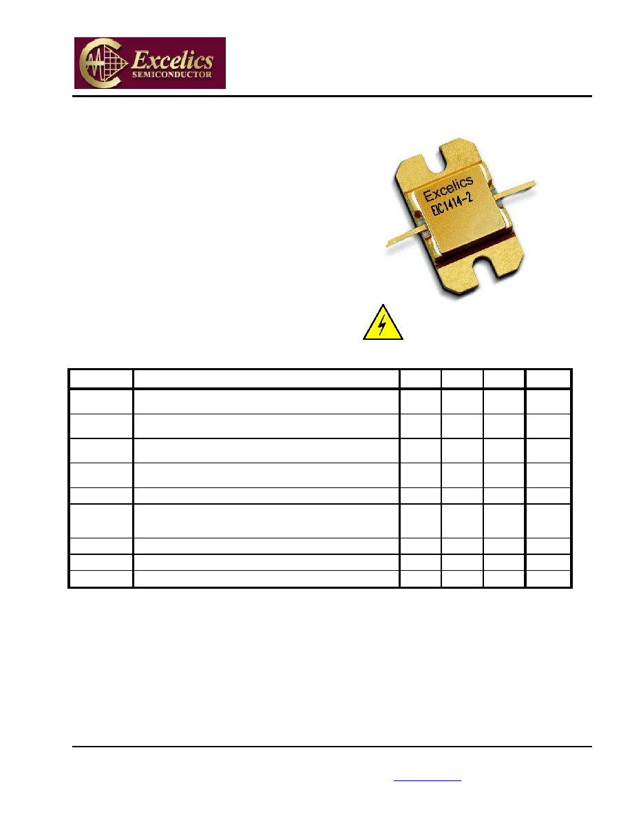
EIC1414-2
Specifications are subject to change without notice.
Excelics Semiconductor, Inc. 310 De Guigne Drive, Sunnyvale, CA 94085
page 1 of 3
Phone: 408-737-1711 Fax: 408-737-1868 Web:
www.excelics.com
Revised March 2004
14.00-14.50 GHz 2-Watt Internally-Matched Power FET
Issued Date: 01-21-04
FEATURES
∑
14.00-14.50
GHz
Bandwidth
∑
Input/Output Impedance Matched to 50 Ohms
∑
+33.5 dBm Output Power at 1dB Compression
∑
6.5 dB Power Gain at 1dB Compression
∑
30% Power Added Efficiency
∑
-42 dBc IM3 at Po = 22.5 dBm SCL
∑
Hermetic Metal Flange Package
∑
100% Tested for DC, RF, and R
TH
DESCRIPTION
The EIC1414-2 is a high power, highly linear,
single stage MFET amplifier in a flange mount
package. This amplifier features Excelics' unique
PHEMT transistor technology.
Caution! ESD sensitive device.
ELECTRICAL CHARACTERISTICS (T
a
= 25
∞
C)
SYMBOL PARAMETERS/TEST
CONDITIONS
1
MIN
TYP
MAX
UNITS
P
1dB
Output Power at 1dB Compression f = 14.00-14.50GHz
V
DS
= 10 V, I
DSQ
= 550mA
32.5 33.5
dBm
G
1dB
Gain at 1dB Compression f = 14.00-14.50GHz
V
DS
= 10 V, I
DSQ
= 550mA
5.5 6.5 dB
G
Gain Flatness f = 14.00-14.50GHz
V
DS
= 10 V, I
DSQ
= 550mA
±0.6
dB
PAE
Power Added Efficiency at 1dB Compression
V
DS
= 10 V, I
DSQ
= 550mA f = 14.00-14.50GHz
30 %
Id
1dB
Drain Current at 1dB Compression f = 14.00-14.50GHz
600
700
mA
IM3
Output 3rd Order Intermodulation Distortion
f = 10 MHz 2-Tone Test; Pout = 22.5 dBm S.C.L
2
V
DS
= 10 V, I
DSQ
65% IDSS
f = 14.50GHz
-38 -42 dBc
I
DSS
Saturated Drain Current
V
DS
= 3 V, V
GS
= 0 V
1040
1440
mA
V
P
Pinch-off Voltage
V
DS
= 3 V, I
DS
= 10 mA
-2.5
-4
V
R
TH
Thermal Resistance
3
11
12
o
C/W
Notes:
1.
Tested with 100 Ohm gate resistor.
2.
S.C.L. = Single Carrier Level.
3.
Overall Rth depends on case mounting.
EIC1414-2
Specifications are subject to change without notice.
Excelics Semiconductor, Inc. 310 De Guigne Drive, Sunnyvale, CA 94085
page 2 of 3
Phone: 408-737-1711 Fax: 408-737-1868 Web:
www.excelics.com
Revised March 2004
Issued Date: 01-21-04
ABSOLUTE MAXIMUM RATINGS FOR CONTINUOUS OPERATION
1,2
SYMBOL CHARACTERISTIC
VALUE
V
DS
Drain to Source Voltage
10 V
V
GS
Gate to Source Voltage
-4.5 V
I
DS
Drain
Current
IDSS
I
GSF
Forward Gate Current
20 mA
P
IN
Input Power
@ 3dB compression
P
T
Total Power Dissipation
10 W
T
CH
Channel
Temperature
150∞C
T
STG
Storage
Temperature
-65/+150∞C
Notes:
1.
Operating the device beyond any of the above ratings may result in permanent damage or reduction of MTTF.
2.
Bias conditions must also satisfy the following equation P
T
< (T
CH
≠T
PKG
)/R
TH
; where T
PKG
= temperature of package, and
P
T
= (V
DS
* I
DS
) ≠ (P
OUT
≠ P
IN
).
EIC1414-2
Specifications are subject to change without notice.
Excelics Semiconductor, Inc. 310 De Guigne Drive, Sunnyvale, CA 94085
page 3 of 3
Phone: 408-737-1711 Fax: 408-737-1868 Web:
www.excelics.com
Revised March 2004
Issued Date: 01-21-04
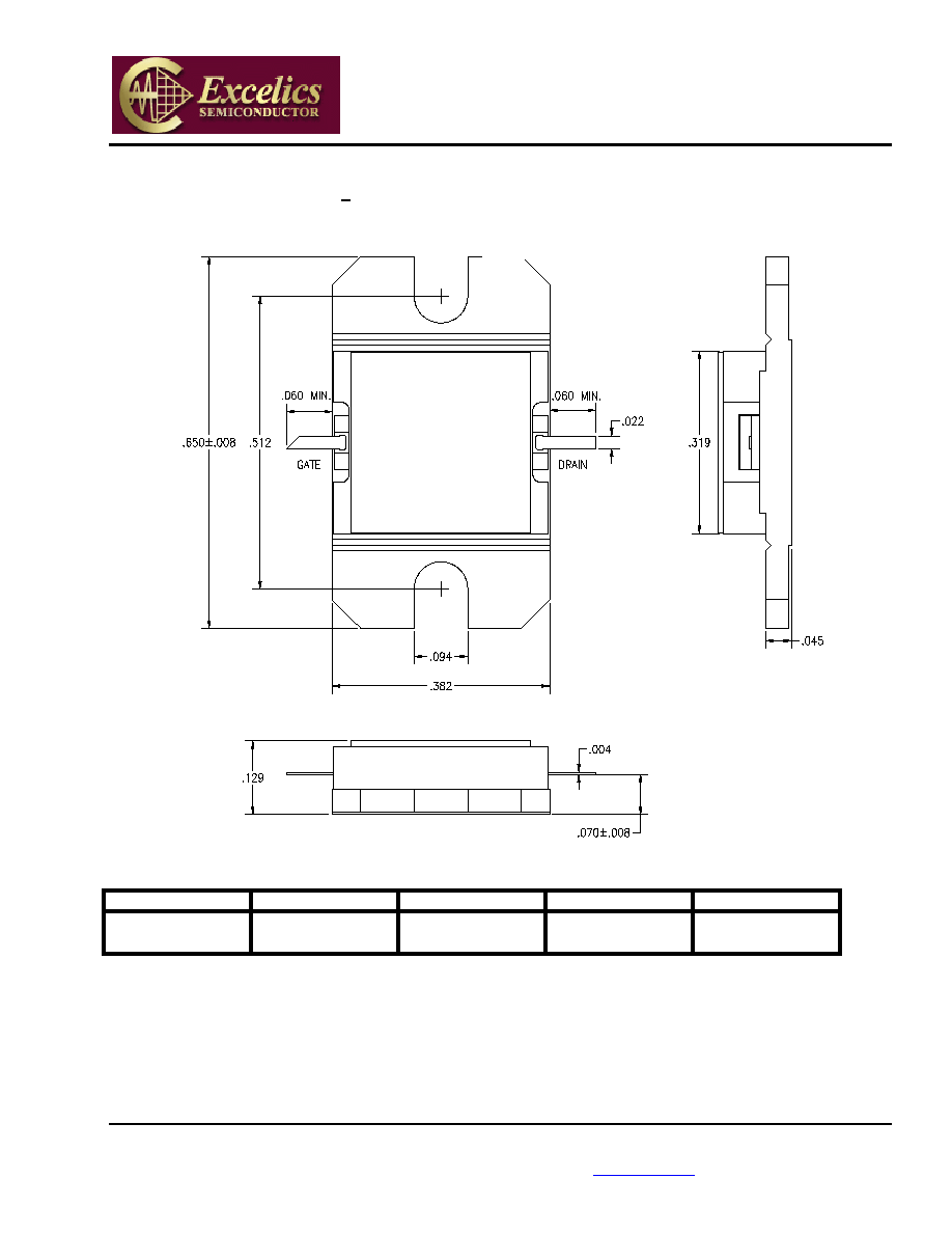
PACKAGE OUTLINE
Dimensions in inches, Tolerance + .005 unless otherwise specified
Excelics
SN
YM
ORDERING INFORMATION
Part Number
Grade
1
f
Test
(GHz)
P
1dB
(min)
IM
3
(min)
2
EIC1414-2 Industrial
14.00-14.50 GHz
32.5
-38.0
Notes: 1. Contact factory for military and hi-rel grades.
2. Exact test conditions are specified in "Electrical Characteristics" table.
EIC1414-2
SOURCE