EIC5359-4
ISSUED
5/15/2006
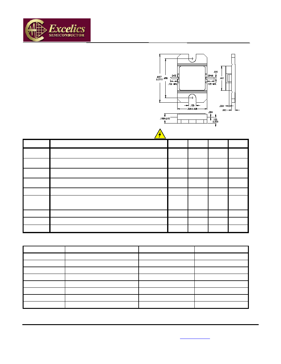
5.3-5.9 GHz 4-Watt Internally Matched Power FET
Specifications are subject to change without notice.
Excelics Semiconductor, Inc. 310 De Guigne Drive, Sunnyvale, CA 94085
page 1 of 1
Phone: 408-737-1711 Fax: 408-737-1868 Web:
www.excelics.com
Revised May 2006
SN
Excelics
YM
FEATURES
�
5.3�
5.9GHz
Bandwidth
�
Input/Output Impedance Matched to 50 Ohms
�
+36.5 dBm Output Power at 1dB Compression
�
10.5 dB Power Gain at 1dB Compression
�
34% Power Added Efficiency
�
Hermetic Metal Flange Package
ELECTRICAL CHARACTERISTICS (T
a
= 25
�
C)
Caution! ESD sensitive device.
SYMBOL PARAMETERS/TEST
CONDITIONS
1
MIN
TYP
MAX
UNITS
P
1dB
Output Power at 1dB Compression f = 5.3-5.9GHz
V
DS
= 10 V, I
DSQ
1100mA
35.5 36.5 dBm
G
1dB
Gain at 1dB Compression f = 5.3-5.9GHz
V
DS
= 10 V, I
DSQ
1100mA
9.5 10.5 dB
G
Gain Flatness f = 5.3-5.9GHz
V
DS
= 10 V, I
DSQ
1100mA
�0.6
dB
PAE
Power Added Efficiency at 1dB Compression
V
DS
= 10 V, I
DSQ
1100mA f = 5.3-5.9GHz
34 %
Id
1dB
Drain Current at 1dB Compression f = 5.3-5.9GHz
1200
1400
mA
IM3
Output 3rd Order Intermodulation Distortion
f=10MHz 2-Tone Test. Pout=25.5 dBm S.C.L
Vds = 10 V, I
DSQ
65% I
DSS
f = 5.9GHz
-43 -46
dBc
I
DSS
Saturated Drain Current
V
DS
= 3 V, V
GS
= 0 V
2000
2500
mA
V
P
Pinch-off Voltage
V
DS
= 3 V, I
DS
= 20 mA
-2.5
-4.0
V
R
TH
Thermal Resistance
3
5.5
6
o
C/W
Note: 1) Tested with 100 Ohm gate resistor. 2) S.C.L. = Single Carrier Level. 3) Overall Rth depends on case mounting.
ABSOLUTE MAXIMUM RATING
1,2
SYMBOLS PARAMETERS
ABSOLUTE
1
CONTINUOUS
2
Vds
Drain-Source Voltage
15
10V
Vgs
Gate-Source Voltage
-5
-4V
Igsf
Forward Gate Current
43.2mA 14.4mA
Igsr
Reserve Gate Current
-7.2mA -2.4mA
Pin
Input Power
35.5dBm
@ 3dB Compression
Tch
Channel Temperature
175
o
C 175
o
C
Tstg
Storage Temperature
-65 to +175
o
C
-65 to +175
o
C
Pt
Total Power Dissipation
25W 25W
Note: 1. Exceeding any of the above ratings may result in permanent damage.
2. Exceeding any of the above ratings may reduce MTTF below design goals.
EIC5359-4
