 | –≠–ª–µ–∫—Ç—Ä–æ–Ω–Ω—ã–π –∫–æ–º–ø–æ–Ω–µ–Ω—Ç: EID1415-8 | –°–∫–∞—á–∞—Ç—å:  PDF PDF  ZIP ZIP |

EID1415-8
Specifications are subject to change without notice.
Excelics Semiconductor, Inc. 310 De Guigne Drive, Sunnyvale, CA 94085
page 1 of 4
Phone: 408-737-1711 Fax: 408-737-1868 Web:
www.excelics.com
Revised January 2004
14.40-15.35 GHz 8-Watt Internally-Matched Power FET
FEATURES
∑
14.40-15.35
GHz
Bandwidth
∑
Input/Output Impedance Matched to 50 Ohms
∑
+39.5 dBm Output Power at 1dB Compression
∑
6.5 dB Power Gain at 1dB Compression
∑
27% Power Added Efficiency
∑
-38 dBc IM3 at Po = 28.5 dBm SCL
∑
Hermetic Metal Flange Package
∑
100% Tested for DC, RF, and R
TH
DESCRIPTION
The EID1415-8 is a high power, highly linear,
single stage MFET amplifier in a flange mount
package. This amplifier features Excelics' unique
PHEMT transistor technology.
Caution! ESD sensitive device.
ELECTRICAL CHARACTERISTICS (T
a
= 25
∞
C)
SYMBOL PARAMETERS/TEST
CONDITIONS
1
MIN
TYP
MAX
UNITS
P
1dB
Output Power at 1dB Compression f = 14.40-15.35GHz
V
DS
= 10 V, I
DSQ
2200mA
38.5 39.5
dBm
G
1dB
Gain at 1dB Compression f = 14.40-15.35GHz
V
DS
= 10 V, I
DSQ
2200mA
5.5 6.5 dB
G
Gain Flatness f = 14.40-15.35GHz
V
DS
= 10 V, I
DSQ
2200mA
±0.6
dB
PAE
Power Added Efficiency at 1dB Compression
V
DS
= 10 V, I
DSQ
2200mA f = 14.40-15.35GHz
27 %
Id
1dB
Drain Current at 1dB Compression f = 14.40-15.35GHz
2800
3600
mA
IM3
Output 3rd Order Intermodulation Distortion
f = 10 MHz 2-Tone Test; Pout = 28.5 dBm S.C.L
2
V
DS
= 10 V, I
DSQ
65% IDSS
f = 15.35GHz
-33 -38
*
dBc
I
DSS
Saturated Drain Current
V
DS
= 3 V, V
GS
= 0 V
4200
5760
mA
V
P
Pinch-off Voltage
V
DS
= 3 V, I
DS
= 40 mA
-1.2
-2.5
V
R
TH
Thermal Resistance
3
3.5
4.0
o
C/W
Notes:
1.
Tested with 100 Ohm gate resistor.
2.
S.C.L. = Single Carrier Level.
3.
Overall Rth depends on case mounting.
*
These devices are available screened for IM3 performance.
Please contact factory with your requirement.
EID1415-8
Specifications are subject to change without notice.
Excelics Semiconductor, Inc. 310 De Guigne Drive, Sunnyvale, CA 94085
page 2 of 4
Phone: 408-737-1711 Fax: 408-737-1868 Web:
www.excelics.com
Revised January 2004
ABSOLUTE MAXIMUM RATINGS FOR CONTINUOUS OPERATION
1,2
SYMBOL CHARACTERISTIC
VALUE
V
DS
Drain to Source Voltage
10 V
V
GS
Gate to Source Voltage
-4.5 V
I
DS
Drain
Current
IDSS
I
GSF
Forward Gate Current
80 mA
P
IN
Input Power
@ 3dB compression
P
T
Total Power Dissipation
35 W
T
CH
Channel
Temperature
150∞C
T
STG
Storage
Temperature
-65/+150∞C
Notes:
1.
Operating the device beyond any of the above ratings may result in permanent damage or reduction of MTTF.
2.
Bias conditions must also satisfy the following equation P
T
< (T
CH
≠T
PKG
)/R
TH
; where T
PKG
= temperature of package, and
P
T
= (V
DS
* I
DS
) ≠ (P
OUT
≠ P
IN
).
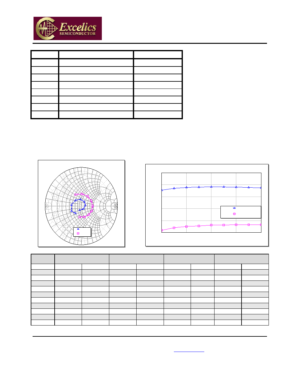
PERFORMANCE DATA
Typical S-Parameters (T= 25∞C, 50
system, de-embedded to edge of package)
V
DS
= 10 V, I
DSQ
2200mA
0
1.0
-1
.0
1.0
10.0
-10.0
10
.0
5.0
-5.0
5.0
2.0
-2
.0
2.
0
3.0
-3.
0
3.0
4.0
-4.0
4.0
0.2
-0.
2
0.2
0.4
-0
.4
0.
4
0.6
-0
.6
0.
6
0.8
-
0
.
8
0
.
8
0
1.0
1.
0
-1.0
10.0
10.0
-1
0.
0
5.0
5.0
-5
.0
2.0
2.
0
-2
.0
3.0
3.
0
-3
.0
4.0
4.0
-4
.0
0.2
0.
2
-0.
2
0.4
0.
4
-0
.4
0.6
0.
6
-0
.6
0.8
0
.
8
-
0
.
8
S11 and S22
Swp Max
16GHz
Swp Min
14GHz
S[1,1] *
EID1415-8
S[2,2] *
EID1415-8
FREQ
--- S11 ---
--- S21 ---
--- S12 ---
--- S22 ---
(GHz)
MAG
ANG
MAG
ANG
MAG
ANG
MAG
ANG
14.00 0.2450 -130.30 1.8778
115.29
0.0393
99.39 0.3370
118.62
14.20
0.2992
-148.84
2.1685
100.98
0.0463
85.54
0.3201
94.18
14.40 0.2904 -173.75 2.3778
82.93
0.0540
66.32 0.3111
68.35
14.60
0.2558
159.14
2.4914
64.05
0.0582
47.41
0.3062
43.95
14.80 0.2117 130.18 2.5593
45.58
0.0635
26.31 0.3090
22.47
15.00
0.1773
98.99
2.5706
27.10
0.0649
8.39
0.3143
2.10
15.20 0.1484 65.63 2.5618
8.94
0.0656
-11.68 0.3119
-17.31
15.40
0.1225
30.44
2.5022
-9.51
0.0675
-31.59
0.3086
-36.12
15.60 0.1012 -7.86 2.4780
-27.74
0.0667
-50.84 0.2987
-55.37
15.80
0.0906
-59.05
2.4084
-46.06
0.0671
-69.19
0.2882
-76.98
16.00 0.1147 -115.00 2.3324
-64.47
0.0677
-88.41 0.2827
-99.97
14
14.5
15
15.5
16
Frequency (GHz)
S21 and S12
-30
-20
-10
0
10
20
S
2
1 an
d S
1
2 (
d
B
)
DB(|S[2,1]|) *
EID1415-8
DB(|S[1,2]|) *
EID1415-8
EID1415-8
Specifications are subject to change without notice.
Excelics Semiconductor, Inc. 310 De Guigne Drive, Sunnyvale, CA 94085
page 3 of 4
Phone: 408-737-1711 Fax: 408-737-1868 Web:
www.excelics.com
Revised January 2004
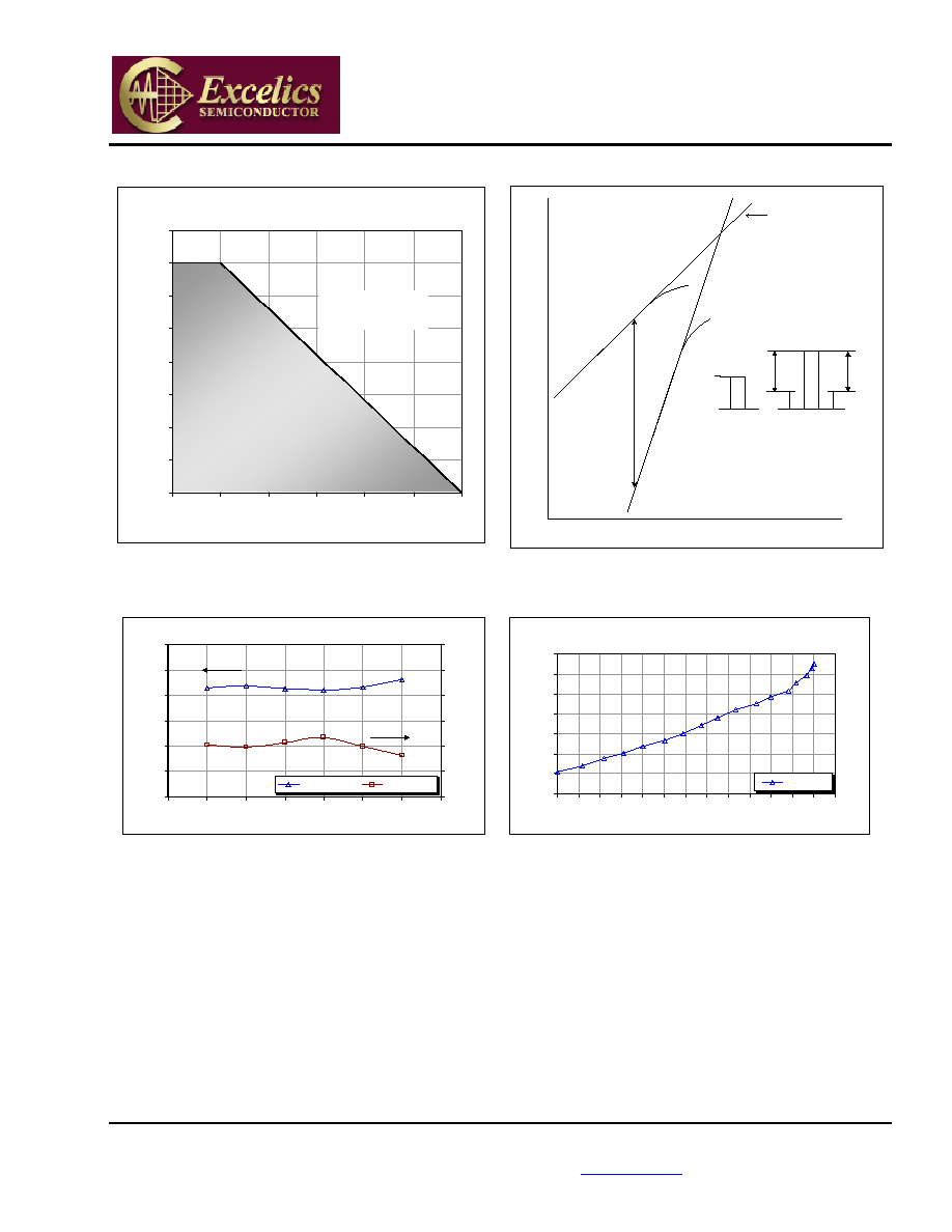
Power De-rating Curve and IM3 Definition
Power Dissipation vs. Temperature
0
5
10
15
20
25
30
35
40
0
25
50
75
100
125
150
Case Temperature (∞C)
T
o
t
a
l
P
o
w
e
r
D
i
s
s
i
pat
i
on (
W
)
Safe Operating
Region
Potentially Unsafe
Operating Region
f1 f2
(2f1-f2) f1 f2 (2f2-f1)
IM3
Pout
Pin
IP
3
= Pout + IM3/2
THIRD-ORDER
INTERCEPT POINT IP3
f1 or f2
(2f2 - f1) or (2f1 - f2)
Pin [S.C.L.] (dBm)
P
o
u
t
[S
.C.L
.]
(
d
B
m
)
IM3
Typical Power Data (V
DS
= 10 V, I
DSQ
= 2200 mA)
Typical IM3 Data (V
DS
= 10 V,
I
DSQ
65% IDSS
)
P-1dB & G-1dB vs Frequency
36
37
38
39
40
41
42
14.2
14.4
14.6
14.8
15.0
15.2
15.4
15.6
Frequency (GHz)
P-1
d
B (
d
Bm
)
5
6
7
8
9
10
11
G
-
1dB
(
d
B
)
P-1dB (dBm)
G-1dB (dB)
IM3 vs Output Power
f1 = 14.50 GHz, f2 = 14.51 GHz
-55
-50
-45
-40
-35
-30
-25
-20
23
24 25
26 27
28 29
30 31
32 33
34 35
36
Pout [S.C.L.] (dBm)
IM
3
(
d
B
c
)
IM3 (dBc)

EID1415-8
Specifications are subject to change without notice.
Excelics Semiconductor, Inc. 310 De Guigne Drive, Sunnyvale, CA 94085
page 4 of 4
Phone: 408-737-1711 Fax: 408-737-1868 Web:
www.excelics.com
Revised January 2004
PACKAGE OUTLINE
Dimensions in inches, Tolerance + .005 unless otherwise specified
Excelics
SN
YM
ORDERING INFORMATION
Part Number
Grade
1
f
Test
(GHz)
P
1dB
(min)
IM
3
(min)
2
EID1415-8 Industrial
14.40-15.35 GHz
38.5
-33.0
Notes: 1. Contact factory for military and hi-rel grades.
2. Exact test conditions are specified in "Electrical Characteristics" table.
EID1415-8
SOURCE