 | –≠–ª–µ–∫—Ç—Ä–æ–Ω–Ω—ã–π –∫–æ–º–ø–æ–Ω–µ–Ω—Ç: ES25P16 | –°–∫–∞—á–∞—Ç—å:  PDF PDF  ZIP ZIP |

E S I
E S I
1
Rev. 0E May 11 , 2006
ES25P16
Excel Semiconductor inc.
ADVANCED INFORMATION
ES25P16
16Mbit CMOS 3.0 Volt Flash Memory
with 75Mhz SPI Bus Interface
ARCHITECTURAL ADVANTAGES
∑ Single power supply operation
- 2.7V -3.6V for read and program operations
∑ Memory Architecture
- Thirty-two sectors with 512 Kb each
∑ Program
- Page program ( up to 256 bytes) in 1.5ms (typical)
- Program cycles are on a page by page basis
∑ Erase
- 0.5s typical sector erase time
- 12s typical bulk erase time
∑ Endurance
-
100,000 cycles per sector (typical)
∑ Data Retention
-
20 years (typical)
∑ Parameter Page
-
256 Byte page independent from main memory
for parameter storage
- Seperate from array, erase time < 20ms
∑ Device ID
- JEDEC standard two-byte electronic signature
- RES instruction one-byte electronic signature for
backward compatibility
- Manufacturer and device type ID
∑ Process Technology
- Manufactured on 0.18um process technology
∑ Package Option
- Industry Standard Pinouts
- 8-pin SO (208mil) package
- All Pb-Free devices are RoHS Compliant
PERFORMANCE CHARACTERISTICS
∑ Speed
-
75Mhz clock rate (maximum)
∑ Power Saving Standby Mode
-
Standby mode 50uA (max)
-
Deep Power Down Mode 1uA (typical)
MEMORY PROTECTION FEATURES
∑ Memory Protection
- W# pin works in conjunction with Status Register Bits
to protect specified memory areas
- Status Register Block Protection Bits (BP2, BP1, BP0)
in status register configure parts of memory as read
only
SOFTWARE FEATURES
∑ SPI Bus Compatible Serial Interface

E S I
E S I
2
Rev. 0E May 11 , 2006
ES25P16
Excel Semiconductor inc.
ADVANCED INFORMATION
The ES25P16 device is a 3.0 volt (2.7V to 3.6V)
single power flash memory device. ES25P16 con-
sists of thirty-two sectors, each with 512 Kb mem-
ory.
Data appears on SI input pin when inputting data
into the memory and on the SO output pin when
outputting data from the memory. The devices are
designed to be programmed in-system with the
standard system 3.0 volt Vcc supply.
The memory can be programmed 1 to 256 bytes at
a time, using the Page Program instruction.
The memory supports Sector Erase and Bulk Erase
instructions.
Each device requires only a 3.0 volt power supply
(2.7V to 3.6V) for both read and write functions.
Internally generated and regulated voltages are pro-
vided for program operations. This device does not
require Vpp supply.
GENERAL PRODUCT DESCRIPTION
BLOCK DIAGRAM
PS
Logic
IO
DATA PATH
Array - R
Array - L
RD
SRAM
XD
E
C
CS
#
SC
K
SI
SO
GND
VCC
W#
HOLD#

E S I
E S I
3
Rev. 0E May 11 , 2006
ES25P16
Excel Semiconductor inc.
ADVANCED INFORMATION
PIN DESCRIPTIONS
Pin
Description
SCK
Serial Clock Input
SI
Serial Data Input
SO
Serial Data Output
CS#
Chip Select Input
W#
Write Protect Input
HOLD#
Hold Input
Vcc
Supply Voltage Input
GND
Ground Input
HOLD#
SO
CS#
W#
GND
VCC
SCK
SI
1
2
3
4
5
6
7
8
Connection Diagrams
8-pin Plastic Small Outline Package (SO)

E S I
E S I
4
Rev. 0E May 11 , 2006
ES25P16
Excel Semiconductor inc.
ADVANCED INFORMATION
SIGNAL DESCRIPTION
Serial Data Output (SO)
This output signal is used to transfer data serially
out of the device. Data is shifted out on the falling
edge of Serial Clock (SCK).
Serial Data Input (SI)
This input signal is used to transfer data serially into
the device. It receives instructions, addresses, and
the data to be programmed. Values are latched on
the rising edge of Serial Clock (SCK).
Serial Clock (SCK)
This input signal provides the timing of the serial
interface. Instructions, addresses, and data present
at the Serial Data Input (SI) are latched on the ris-
ing edge of Serial Clock (SCK). Data on Serial Data
Output (SO) changes after the falling edge of Serial
Clock (SCK).
Chip Select (CS#)
When this input signal is high, the device is dese-
lected and Serial Data Output (SO) is at high
impedance. Unless an internal Program, Erase or
Write Status Register cycle is in progress, the
device will be in Standby mode. Driving Chip Select
(CS#) Low enables the device, placing it in the
active power mode.
After power-up, a falling edge on Chip Select (CS#)
is required prior to the start of any instruction.
Hold (HOLD#)
The Hold (HOLD#) signal is used to pause any
serial communications with the device without
deselecting the device.
During the Hold instruction, the Serial Data Output
(SO) is high impedance, and Serial Data Input (SI)
and Serial Clock (SCK) are Don't Care.
To start the Hold condition, the device must be
selected, with Chip Select (CS#) driven Low.
Write Protect (W#)
The main purpose of this input signal is to freeze
the size of the area of memory that is protected
against program or erase instructions (as specified
by the values in the BP2, BP1 and BP0 bits of the
Status Register).
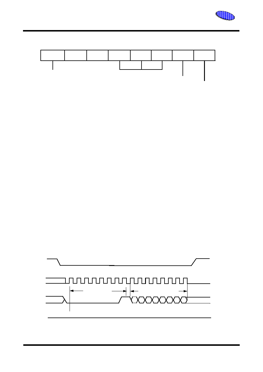
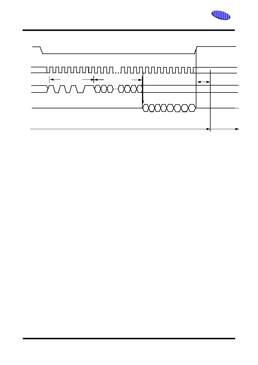
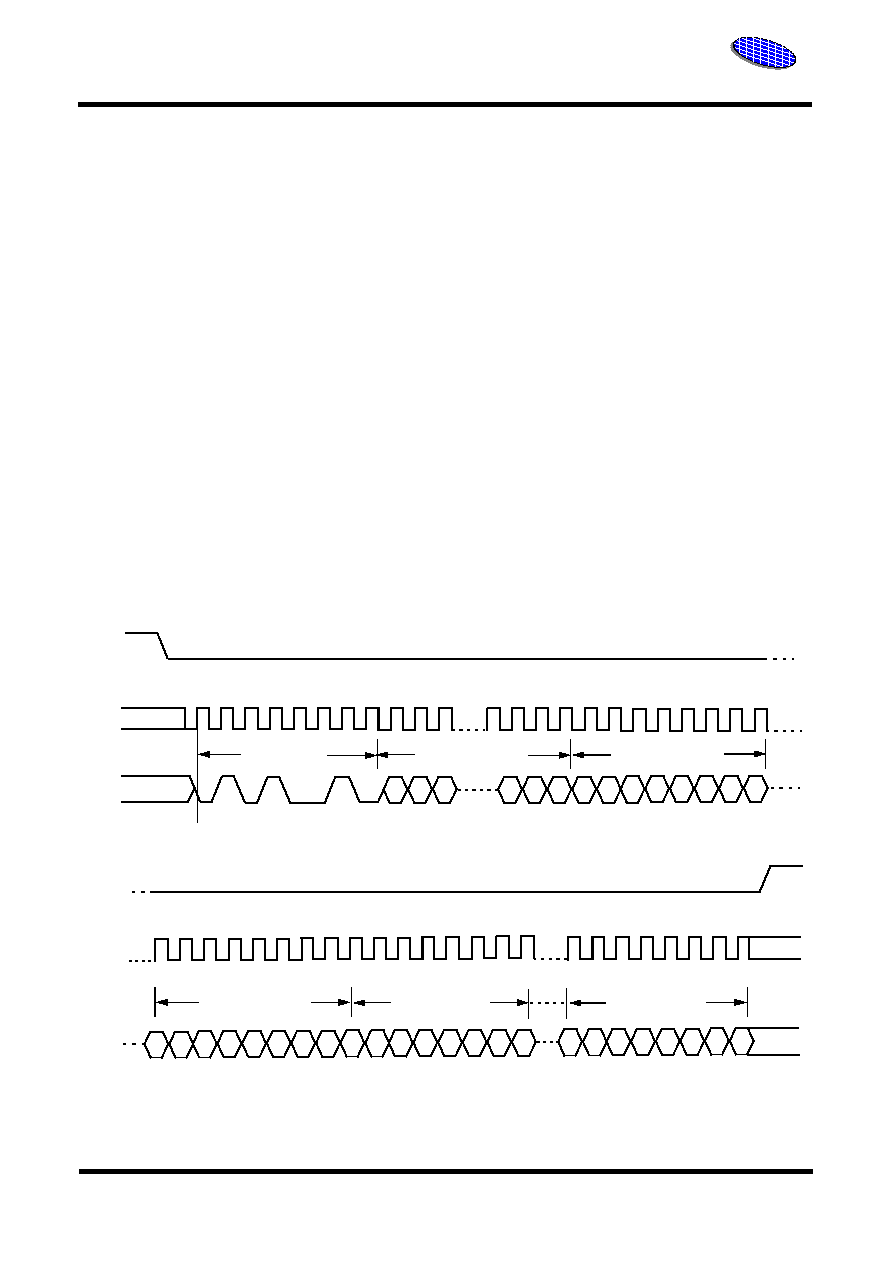
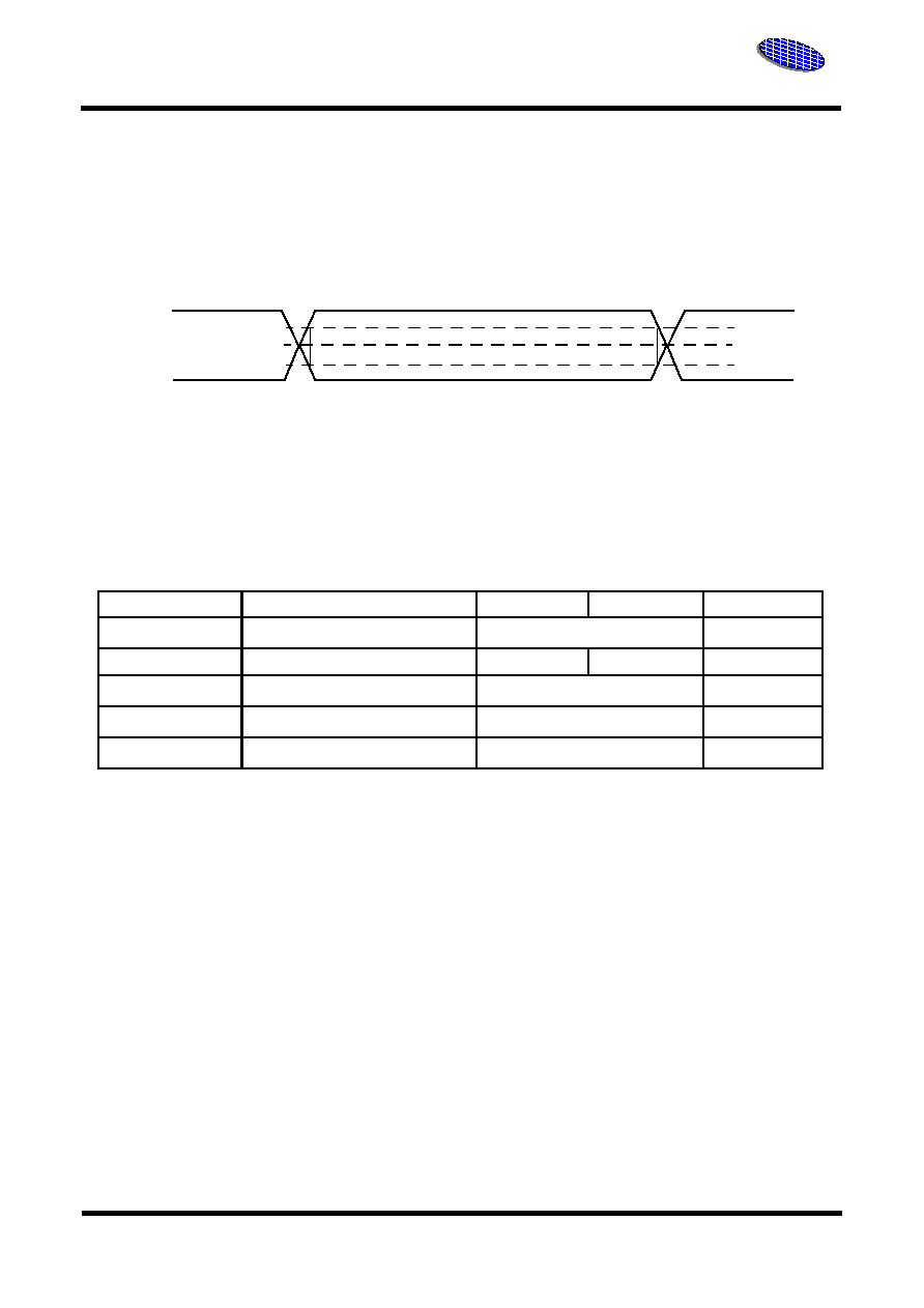
SPI MODES
These devices can be driven by a microcontroller
with its SPI peripheral running in either of the two fol-
lowing modes :
CPOL = 0, CPHA = 0
CPOL = 1, CPHA = 1
For these two modes, input data is latched in on the
rising edge of Serial Clock (SCK), and output data is
available from the falling edge of Serial Clock (SCK).
The difference between the two modes, as shown in
Figure 1, is the clock polarity when the bus master is
in Standby and not transferring data:
SCK remains at 0 for (CPOL = 0, CPHA = 0)
SCK remains at 1 for (CPOL = 1, CPHA = 1)
OPERATING FEATURES
All data into and out of the device is shifted in 8-bit
chunks.
Page Programming
To program one data byte, two instructions are
required : Write Enable (WREN), which is one byte,
and a Page Program (PP) sequence, which consists
of four bytes plus data. This is followed by the inter-
nal program cycle. To spread this overhead, the
Page Program (PP) instruction allows up to 256
bytes to be programmed at a time (changing bits
from 1 to 0), provided that they lie in consecutive
addresses on the same page of memory.
Sector Erase, or Bulk Erase
The Page Program (PP) instruction allows bits to be
programmed from 1 to 0. Before this can be applied,
the bytes of the memory need to be first erased to all
1's (FFh) before any programming. This can be
achieved in two ways :1) a sector at a time using the
Sector Erase (SE) instruction, or 2) throughout the
entire memory, using the Bulk Erase (BE) instruc-
tion.
E S I
E S I
5
Rev. 0E May 11 , 2006
ES25P16
Excel Semiconductor inc.
ADVANCED INFORMATION
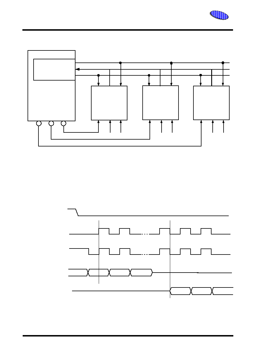
Figure 1. Bus Master and Memory Devices on the SPI Bus
SCK
SPI Interface with
(CPOL, CPHA) =
(0,0) or (1,1)
Bus Master
CS1 CS2 CS3
SPI Memory
Device
SPI Memory
Device
SPI Memory
Device
SO
SI
SCK
SO
SI
SCK
SO
SI
SCK
SO
SI
CS#
CS#
CS#
W#
W#
W#
HOLD#
HOLD#
HOLD#
Note :
The Write Protect (W#) and Hold (HOLD#) signals should be driven, High or Low as appropriate
Figure 2. SPI Modes Supported
SCK
CS#
SCK
SI
MSB
SO
CPOL CPHA
0 0
1 1
MSB

E S I
E S I
6
Rev. 0E May 11 , 2006
ES25P16
Excel Semiconductor inc.
ADVANCED INFORMATION
Polling During a Write, Program, or
Erase Cycle
A further improvement in the time to Write Status
Register (WRSR), Program(PP) or Erase (SE or BE)
can be achieved by not waiting for the worst-case
delay. The Write in Progress (WIP) bit is provided in
the Status Register so that the application program
can monitor its value, polling it to establish when the
previous Write cycle, Program cycle, or Erase cycle
is complete.
Active Power and Standby Power Modes
When Chip Select (CS#) is Low, the device is
enabled, and in the Active Power mode. When Chip
Select (CS#) is High, the device is disabled, but
could remain in the Active Power mode until all inter-
nal cycles have completed (Program, Erase, Write
Status Register). The device then goes into the
Standby Power mode. The device consumption
drops to I
SB
. This can be used as an extra Deep
Power Down on mechanism, when the device is not
in active use, to protect the device from inadvertent
Write, Program, or Erase instructions.
Status Register
The Status Register contains a number of status and
control bits, as shown in Figure 7, that can be read
or set (as appropriate) by specific instructions
WIP bit
The Write In Progress (WIP) bit indicates whether
the memory is busy with a Write Status Register,
Program or Erase cycle.
WEL bit
The Write Enable Latch (WEL) bit indicates the sta-
tus of the internal Write Enable Latch.
BP2, BP1, BP0 bits
The Block Protect (BP2, BP1, BP0) bits are non-vol-
atile. They define the size of the area to be software
protected against Program and Erase instructions.
SRWD bit
The Status Register Write Disable (SRWD) bit is
operated in conjunction with the Write Protect (W#)
signal. The Status Register Write Disable (SRWD)
bit and Write Protect (W#) signal allow the device to
be put in the Hardware Protected mode. In this
mode, the non-volatile bits of the Status Register
(SRWD, BP2, BP1, BP0) become read-only bits.
Hold Condition Modes
The Hold (HOLD#) signal is used to pause any serial
communications with the device without resetting the
clocking sequence. Hold (HOLD#) signal gates the
clock input to the device. However, taking this signal
Low does not terminate any Write Status Register,
Program or Erase cycle that is currently in progress.
To enter the Hold condition, the device must be
selected, with Chip Select (CS#) Low. The Hold con-
dition starts on the falling edge of the Hold (HOLD#)
signal, provided that this coincides with Serial Clock
(SCK) being Low (as shown in Figure 3).
The Hold condition ends on the rising edge of the
Hold (HOLD#) signal, provided that this coincides
with Serial Clock (SCK) being Low.
Figure 3. Hold Condition Activation
SCK
HOLD#
Hold Condition
(Standard use)
Hold Condition
(non-standard use)
E S I
E S I
7
Rev. 0E May 11 , 2006
ES25P16
Excel Semiconductor inc.
ADVANCED INFORMATION
Protection Modes
The SPI memory device boasts the following data
protection mechanisms
1) All instructions that modify data must be preceded
by a Write Enable(WREN) instruction to set the
Write Enable Latch (WEL) bit. This bit is returned to
its reset state by the following events :
- Power-up
- WRDI instruction completion
- WRSR instruction completion
- PP instruction completion
- SE instruction completion
- BE instruction completion
2) The Block Protect (BP2, BP1, BP0) bits allow part
of the memory to be configured as read-only. This is
the Software Protected Mode (SPM).
3) The Write Protect (W#) signal works in coopera-
tion with the Status Register Write Disable (SRWD)
bit to enable write-protection. This is the Hardware
Protected Mode (HPM).
4) Program, Erase and Write Status Register instruc-
tions are checked to verify that they consist of a
number of clock pulses that is a multiple of eight,
before they are accepted for execution.
If the falling edge does not coincide with Serial Clock
(SCK) being Low, the Hold condition starts after
Serial Clock (SCK) next goes Low. Similarly, If the
rising edge does not coincide with Serial Clock
(SCK) being Low, the Hold condition ends after
Serial Clock (SCK) next goes Low (Figure 3).
During the Hold condition, the Serial Data Output
(SO) is high impedance, and Serial Data Input (SI)
and Serial Clock (SCK) are Don't Care.
Normally, the device remains selected, with Chip
Select (CS#) driven Low, for the entire duration of
the Hold condition. This ensures that the state of the
internal logic remains unchanged from the moment
of entering the Hold condition.
If Chip Select (CS#) goes High while the device is in
the Hold condition, this has the effect of resetting the
internal logic of the device. To restart communication
with the device, it is necessary to drive Hold
(HOLD#) High, and then to drive Chip Select (CS#)
Low. This prevents the device from going back to the
Hold condition.
Table 1. Protected Area Sizes
Protected Memory
Area (Top Level)
Status Register Content
Memory Content
BP2 Bit
BP1 Bit
BP0 Bit
Protected Area
Unprotected Area
0
0
0
0
none
000000 ~ 1FFFFF
1 / 32
0
0
1
1F0000 ~ 1FFFFF
000000 ~ 1EFFFF
1 / 16
0
1
0
1E0000 ~ 1FFFFF
000000 ~ 1DFFFF
1 / 8
0
1
1
1C0000 ~ 1FFFFF
000000 ~ 1BFFFF
1 / 4
1
0
0
180000 ~ 1FFFFF
000000 ~ 17FFFF
1 / 2
1
0
1
100000 ~ 1FFFFF
000000 ~ 0FFFFF
All
1
1
0
000000 ~ 1FFFFF
+ parameter page
none
All
1
1
1
000000 ~ 1FFFFF
+ parameter page
none

E S I
E S I
8
Rev. 0E May 11 , 2006
ES25P16
Excel Semiconductor inc.
ADVANCED INFORMATION
MEMORY ORGANIZATION
The memory is organized as :
- ES25P16 : Thirty-two sectors of 512 Kbit each
- Each page can be individually programmed
(
bits are programmed from 1 to 0
).
- The device is Sector or Bulk erasable (bits are erased from 0 to 1)
Table 2. Sector Address
Sector
Address Range
SA31
1F0000h
1FFFFFh
SA30
1E0000h
1EFFFFh
SA29
1D0000h
1DFFFFh
SA28
1C0000h
1CFFFFh
SA27
1B0000h
1BFFFFh
SA26
1A0000h
1AFFFFh
SA25
190000h
19FFFFh
SA24
180000h
18FFFFh
SA23
170000h
17FFFFh
SA22
160000h
16FFFFh
SA21
150000h
15FFFFh
SA20
140000h
14FFFFh
SA19
130000h
13FFFFh
SA18
120000h
12FFFFh
SA17
110000h
11FFFFh
SA16
100000h
10FFFFh
SA15
0F0000h
0FFFFFh
SA14
0E0000h
0EFFFFh
SA13
0D0000h
0DFFFFh
SA12
0C0000h
0CFFFFh
SA11
0B0000h
0BFFFFh
SA10
0A0000h
0AFFFFh
SA9
090000h
09FFFFh
SA8
080000h
08FFFFh
SA7
070000h
07FFFFh
SA6
060000h
06FFFFh
SA5
050000h
05FFFFh
SA4
040000h
04FFFFh
SA3
030000h
03FFFFh
SA2
020000h
02FFFFh
SA1
010000h
01FFFFh
SA0
000000h
00FFFFh

E S I
E S I
9
Rev. 0E May 11 , 2006
ES25P16
Excel Semiconductor inc.
ADVANCED INFORMATION
INSTRUCTIONS
All instructions, addresses, and data are shifted in
and out of the device, starting with the most signifi-
cant bit. Serial Data Input (SI) is sampled on the first
rising edge of Serial Clock (SCK) after Chip Select
(CS#) is driven Low. Then, the one byte instruction
code must be shifted in to the device, most signifi-
cant bit first, on Serial Data Input (SI), each bit being
latched on the rising edges of Serial Clock (SCK).
The instruction set is listed in Table 3.
Every instruction sequence starts with a one byte
instruction code. Depending on the instruction, this
might be followed by address bytes, or by data
bytes, or by both or none. Chip Select (CS#) must be
driven High after the last bit of the instruction
sequence has been shifted in.
In the case of a Read Data Bytes (READ), Read Sta-
tus Register (RDSR), Read Data Bytes at higher
speed (FAST_READ), Read Identification (RDID) ,
Read Manufacturer and Device ID (RDMD), Read
Parameter Page (RDPARA) and Fast Read Parame-
ter Page (FRDPARA) instructions, the shifted-in
instruction sequence is followed by a data-out
sequence.
Chip Select (CS#) can be driven High after any bit
of the data-out sequence is being shifted out to ter-
minate the transaction.
In the case of a Page Program (PP), Program
Parameter Page (PPP), Sector Erase (SE), Bulk
Erase (BE), Parameter Page Erase(PE), Write Sta-
tus Register (WRSR), Write Enable (WREN), Deep
Power Down (DP) or Write Disable (WRDI) instruc-
tion, Chip Select (CS#) must be driven High exactly
at a byte boundary, otherwise the instruction is
rejected, and is not executed. That is, Chip Select
(CS#) must driven High when the number of clock
pulses after Chip Select (CS#) being driven Low is
an exact multiple of eight.
All attempts to access the memory array during a
Write Status Register cycle, Program cycle or Erase
cycle are ignored, and the internal Write Status
Register cycle, Program cycle or Erase cycle con-
tinues unaffected.
E S I
E S I
10
Rev. 0E May 11 , 2006
ES25P16
Excel Semiconductor inc.
ADVANCED INFORMATION
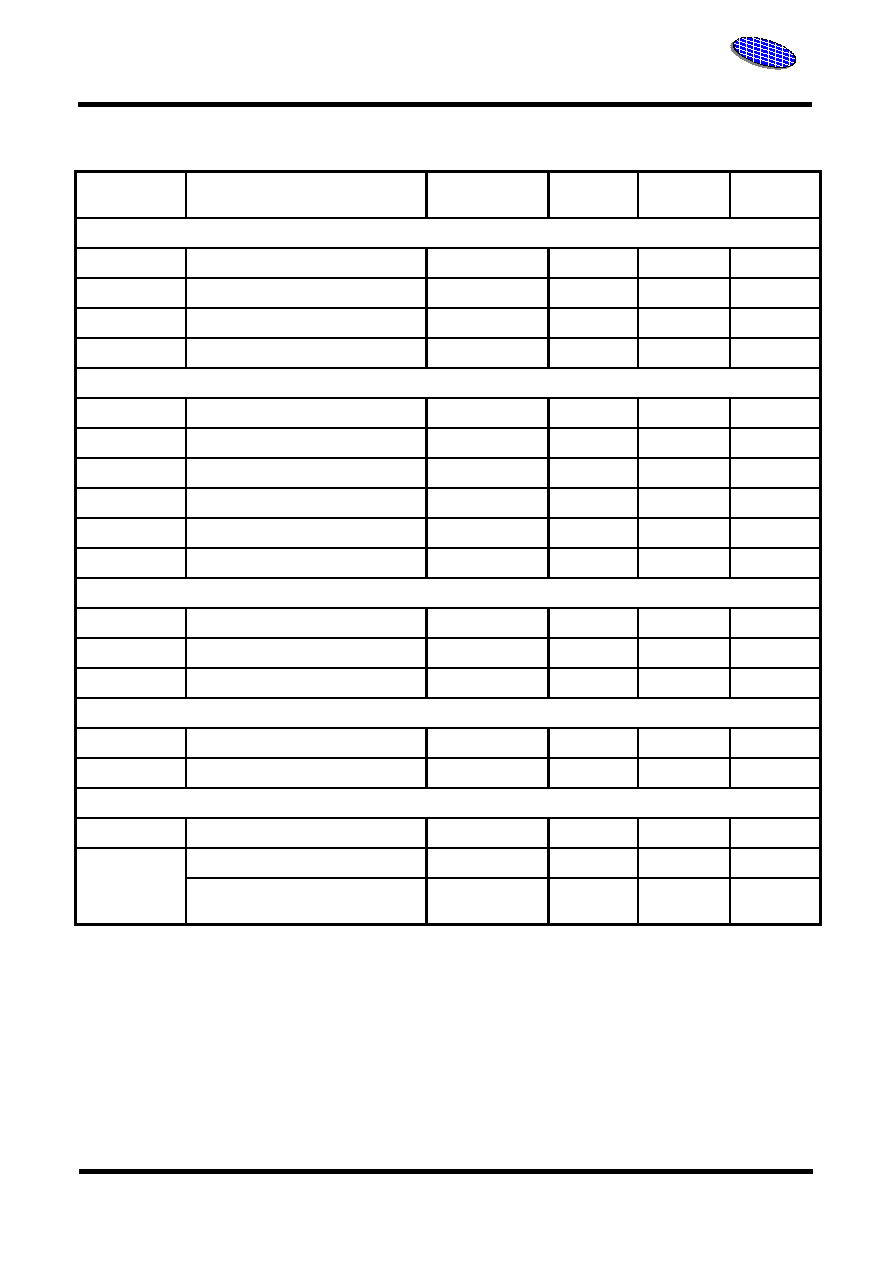
Table 3. Instruction Set
Instruction
Description
One-Byte
Instruction Code
Address
Bytes
Dummy
Byte
Data Bytes
Status Register Operations
WREN
Write Enable
06H (0000 0110)
0
0
0
WRDI
Write Disable
04H (0000 0100)
0
0
0
RDSR
Read from Status Register
05H (0000 0101)
0
0
1 to Infinity
WRSR
Write to Status Register
01H (0000 0001)
0
0
1
Read Operations
READ
Read Data Bytes
03H (0000 0011)
3
0
1 to Infinity
FAST_READ
Read Data Bytes at Higher Speed
0BH (0000 1011)
3
1
1 to Infinity
RDID
Read Identification
9FH (1001 1111)
0
0
1 to 3
RDMD
Read Manufacturer and Device ID
90H (1001 0000)
0
3
1 to Infinity
RDPARA
Read Parameter Page
53H (0101 0011)
3
0
1 to Infinity
FRDPARA
Fast Read Parameter Page
5BH (0101 1011)
3
1
1 to Infinity
Erase Operations
SE
Sector Erase
D8H (1101 1000)
3
0
0
BE
Bulk (Chip) Erase
C7H (1100 0111)
0
0
0
PE
Erase Parameter Page
D5H (1101 0101)
0
0
0
Program Operations
PP
Page Program
02H (0000 0010)
3
0
1 to 256
PPP
Program Parameter Page
52H (0101 0010)
3
0
1 to 256
Deep Power Down Savings Mode Operations
DP
Deep Power Down
B9H (1011 1001)
0
0
0
RES
Release from Deep Power Down
ABH (1010 1011)
0
0
0
Release from Deep Power Down and
Read Electronic Signature
ABH (1010 1011)
0
3
1 to Infinity

E S I
E S I
11
Rev. 0E May 11 , 2006
ES25P16
Excel Semiconductor inc.
ADVANCED INFORMATION
0 0 0 0 0 1 0 0
0 0 0 0 0 1 1 0
Write Enable (WREN)
The Write Enable (WREN) instruction (Figure 4) sets
the Write Enable Latch (WEL) bit. The Write Enable
Latch (WEL) bit must be set prior to every Page Pro-
gram (PP or PPP), Erase (SE, BE or PE) and Write
Status Register (WRSR) instruction. The Write
Enable (WREN) instruction is entered by driving
Chip Select (CS#) Low, sending the instruction code,
and then driving Chip Select (CS#) High.
Write Disable (WRDI)
The Write Disable (WRDI) instruction (Figure 5)
resets the Write Enable Latch (WEL) bit. The Write
Disable (WRDI) instruction is entered by driving Chip
Select (CS#) Low, sending the instruction code, and
then driving Chip Select (CS#) High.
The Write Enable (WEL) bit is reset under the follow-
ing conditions :
- Power-up
- WRDI instruction completion
- WRSR instruction completion
- PP instruction completion
- SE instruction completion
- BE instruction completion
0 1 2 3 4 5 6 7
Figure 4. Write Enable ( WREN ) Instruction Sequence
SCK
CS#
SI
SO
Instruction
High Impedance
0
1 2 3 4 5 6 7
Figure 5. Write Disable ( WRDI ) Instruction Sequence
SCK
CS#
SI
SO
Instruction
High Impedance
E S I
E S I
12
Rev. 0E May 11 , 2006
ES25P16
Excel Semiconductor inc.
ADVANCED INFORMATION
0 0 0 0 0 1 0 1
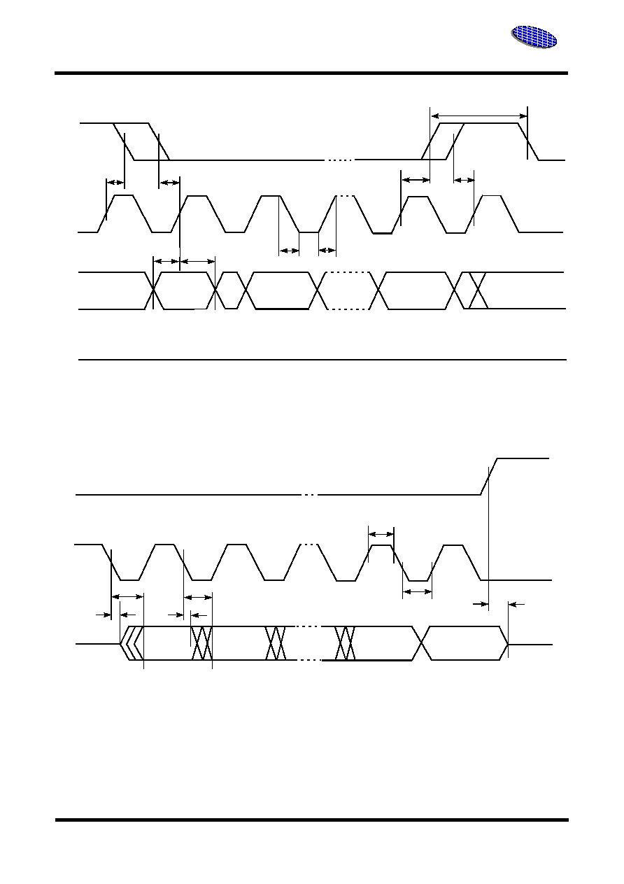
Read Status Register (RDSR)
The Read Status Register (RDSR) instruction allows
the Status Register to be read. The Status Register
may be read at any time, even while a Program,
Erase, or Write Status Register cycle is in progress.
When one of these cycles is in progress, it is recom-
mended to check the Write In Progress (WIP) bit
before sending a new instruction to the device. It is
also possible to read the Status Register continu-
ously, as shown in Figure 6.
The status and control bits of the Status Register are
as follows :
WIP bit
The Write In Progress (WIP) bit indicates whether
the memory is busy with a Write Status Register,
Program or Erase cycle. This bit is a read only bit
and is read by executing a RDSR instruction. If this
bit is 1, such a cycle is in progress, if it is 0, no such
cycle is in progress.
WEL bit
The Write Enable Latch (WEL) bit indicates the sta-
tus of the internal Write Enable Latch. When set to 1,
the internal Write Enable Latch is set; when set to 0,
the internal Write Enable Latch is reset and no Write
Status Register, Program or Erase instruction is
accepted.
BP2, BP1, BP0 bits
The Block Protect (BP2, BP1, BP0) bits are non-vol-
atile. They define the size of the area to be software
protected against Program and Erase instructions.
These bits are written with the Write Status Register
(WRSR) instruction. When one or both of the Block
Protect (BP2, BP1, BP0) bits is set to 1, the relevant
memory area (as defined in Table 1) becomes pro-
tected against Page Program (PP), and Sector
Erase (SE) instructions. The Block Protect (BP2,
BP1, BP0) bits can be written provided that the
Hardware Protected mode has not been set. The
Bulk Erase (BE) instruction is executed if, and only
if, all Block Protect (BP2, BP1, BP0) bits are 0.
SRWD bit
The Status Register Write Disable (SRWD) bit is
operated in conjunction with the Write Protect (W#)
signal. The Status Register Write Disable (SRWD)
bit and Write Protect (W#) signal allow the device to
be put in the Hardware Protected mode (when the
Status Register Write Disable (SRWD) bit is set to 1,
and Write Protect (W#) is driven Low). In this mode,
the non-volatile bits of the Status Register (SRWD,
BP2, BP1, BP0) become read-only bits and the
Write Status Register (WRSR) instruction is no
longer accepted for execution.
Figure 6. Read Status Register (RDSR) Instruction Sequence
SCK
CS#
SI
SO
Status Register Out
Status Register Out
MSB
MSB
7
Instruction
High Impedance
0 1 2 3 4 5 6 7 8 9 10 11 12 13 14 15
6
5
4
3
2
1
0
7
6
5
4
3
2
1
0
E S I
E S I
13
Rev. 0E May 11 , 2006
ES25P16
Excel Semiconductor inc.
ADVANCED INFORMATION
0
0 0 0 0 0 0 1
Write Status Register (WRSR)
The Write Status Register (WRSR) instruction
allows new values to be written to the Status Regis-
ter. Before it can be accepted, a Write Enable
(WREN) instruction must previously have been
executed. After the Write Enable (WREN) instruc-
tion has been decoded and executed, the device
sets the Write Enable Latch (WEL).
The Write Status Register (WRSR) instruction is
entered by driving Chip Select (CS#) Low, followed
by the instruction code and the data byte on Serial
Data Input (SI).
The instruction sequence is shown in Figure 8.
The Write Status Register (WRSR) instruction has
no effect on bits b6, b5, b1 and b0 of the Status
Register. Bits b6, b5 are always read as 0.
Chip Select (CS#) must be driven High after the
eighth bit of the data byte has been latched in. If
not, the Write Status Register (WRSR) instruction is
not executed.
As soon as Chip Select (CS#) is driven High, the
self-timed Write Status Register cycle (whose dura-
tion is t
w
) is initiated. While the Write Status Regis-
ter cycle is in progress, the Status Register may still
be read to check the value of the Write In Progress
(WIP) bit. The Write In Progress (WIP) bit is 1 dur-
ing the self-timed Write Status Register cycle, and
is 0 when it is completed. At some unspecified time
before the cycle is completed, the Write Enable
Latch (WEL) is reset.
The Write Status Register (WRSR) instruction
allows the user to change the values of the Block
Protect (BP2, BP1, BP0) bits, to define the size of
the area that is to be treated as read-only, as
defined in Table 1. The Write Status Register
(WRSR) instruction also allows the user to set or
reset the Status Register Write Disable (SRWD) bit
in accordance with the Write Protect (W#) signal.
The Status Register Write Disable (SRWD) bit and
Write Protect (W#) signal allow the device to be put
in the Hardware Protected Mode (HPM). The Write
Status Register (WRSR) instruction cannot be exe-
cuted once the Hardware Protected Mode (HPM) is
entered.
Figure 7. Status Register Format
SRWD 0 0 BP2 BP1 BP0 WEL WIP
Status Register Write Disable
Block Protect Bits
Write Enable Latch Bit
Write In Progress Bit
b7 b6 b5 b4 b3 b2 b1 b0
Figure 8. Write Status Register (WRSR) Instruction Sequence
Status Register In
SCK
CS#
SI
SO
Instruction
High Impedance
0
1 2 3 4 5 6 7 8 9 10 11 12 13 14 15
MSB
7
6
5
4
3
2
1
0

E S I
E S I
14
Rev. 0E May 11 , 2006
ES25P16
Excel Semiconductor inc.
ADVANCED INFORMATION
The protection features of the device are summa-
rized in Table 4.
When the Status Register Write Disable (SRWD) bit
of the Status Register is 0 (its initial delivery state),
it is possible to write to the Status Register provided
that the Write Enable Latch (WEL) bit has previ-
ously been set by a Write Enable (WREN) instruc-
tion, regardless of the whether Write Protect (W#) is
driven High or Low.
When the Status Register Write Disable (SRWD) bit
of the Status Register is set to 1, two cases need to
be considered, depending on the state of Write Pro-
tect (W#).
1) If Write Protect (W#) is driven High, it is possible
to write to the Status Register provided that the
Write Enable Latch (WEL) bit has previously been
set by a Write Enable (WREN) instruction.
2) If Write Protect (W#) is driven Low, it is not possi-
ble to write to the Status Register even if the Write
Enable Latch (WEL) bit has previously been set by
a Write Enable (WREN) instruction. (Attempts to
write to the Status Register are rejected, and are
not accepted for execution).
As a consequence, all the data bytes in the memory
area that are software protected (SPM) by the
Block Protect (BP2, BP1, BP0) bits of the Status
Register, are also hardware protected against data
modification.
Regardless of the order of the two events, the
Hardware Protected Mode (HPM) can be entered :
1) by setting the Status Register Write Disable
(SRWD) bit after driving Write Protect (W#) Low
2) or by driving Write Protect (W#) Low after setting
the Status Register Write Disable (SRWD) bit.
The only way to exit the Hardware Protected Mode
(HPM) once entered is to pull Write Protect (W#)
High.
If Write Protect (W#) is permanently tied High, the
Hardware Protected Mode (HPM) can never be
activated, and only the Software Protected Mode
(SPM), using the Block Protect (BP2, BP1, BP0)
bits of the Status Register, can be used.
Table 4. Protection Modes
W# Signal SRWD Bit
Mode
Write Protection of the Sta-
tus Register
Protected Area
(See Note)
Unprotected Area
(See Note)
1
1
Software
Protected
(SPM)
Status Register is Writable
(if the WREN instruction has
set the WEL bit).
The values in the SRWD,
BP2, BP1 and BP0 bits can
be changed.
Protected against
Page Program and
Erase(SE, BE,PE)
Ready to accept Page
Program and Sector
Erase Instructions
1
0
0
0
0
1
Hardware
Protected
(HPM)
Status Register is Hardware
write protected.
The values in the SRWD,
BP2, BP1 and BP0 bits can-
not be changed
Protected against
Page Program and
Erase (SE,BE,PE)
Ready to accept Page
Program and Sector
Erase Instructions
Note:
1. As defined by the values in the Block Protected (BP2, BP1, BP0) bits of the Status Register, as shown in Table 1.
E S I
E S I
15
Rev. 0E May 11 , 2006
ES25P16
Excel Semiconductor inc.
ADVANCED INFORMATION
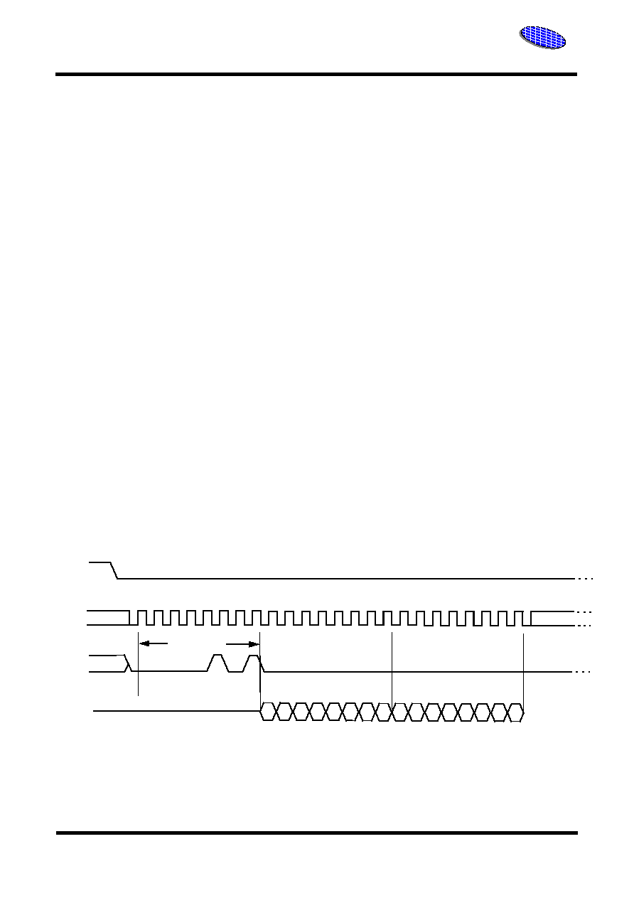
Read Data Bytes (READ)
The READ instruction reads the memory at the
specified SCK frequency (fsck) with a maximum
speed of 40MHz.
The device is first selected by driving Chip Select
(CS#) Low. The instruction code for the Read Data
Bytes (READ) instruction is followed by a 3-byte
address (A23 - A0), each bit being latched-in during
the rising edge of Serial Clock (SCK). Then the
memory contents, at the address, are shifted out on
Serial Data Output (SO), each bit being shifted out,
at a frequency fsck, during the falling edge of Serial
Clock (SCK).
The instruction sequence is shown in Figure 9. The
first byte addressed can be at any location. The
address automatically increments to the next higher
address after each byte of data is shifted out. The
whole memory can, therefore, be read with a single
Read Data Bytes (READ) instruction. When the
highest address is reached, the address counter
rolls over to 00000h, allowing the read sequence to
be continued indefinitely.
The Read Data Bytes (READ) instruction is termi-
nated by driving Chip Select (CS#) High. Chip Select
(CS#) can be driven High at any time during data
output. Any Read Data Bytes (READ) instruction,
while a Program, Erase, or Write cycle is in
progress, is rejected without having any effect on the
cycle that is in progress.
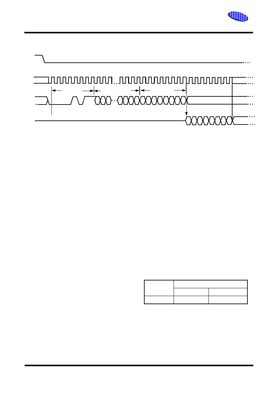
Read Data Bytes at Higher Speed
(FAST_ READ)
The FAST_READ instruction reads the memory at
the specified SCK frequency (fsck) with a maximum
speed of 75 MHz. The device is first selected by
driving Chip Select (CS#) Low. The instruction code
for FAST_READ instruction is followed by a 3-byte
address (A23 - A0) and a dummy byte, each bit
being latched in during the rising edge of Serial
Clock (SCK). Then the memory contents, at that
address, are shifted out on Serial Data Output
(SO), each bit being shifted out. at a maximum fre-
quency Fsck, during the falling edge of Serial Clock
(SCK).
The instruction sequence is shown in Figure 10.
The first byte addressed can be at any location.
The address automatically increments to the next
higher address after each byte of data is shifted
out. The whole memory can, therefore, be read with
a single FAST_READ instruction.
When the highest address is reached, the address
counter rolls over to 00000h, allowing the read
sequence to be continued indefinitely
The FAST_READ instruction is terminated by driv-
ing Chip Select (CS#) High. Chip Select (CS#) can
be driven High at any time during data output. Any
FAST_READ instruction, while an Erase, Program
or Write cycle is in progress, is rejected without
having any effects on the cycle that is in progress.
0
1
2
3 4
5 6
7
8
9 10
28 29
30 31
32
33 34 35
36
37 38 39
Figure 9. Read Data Bytes (READ) Instruction Sequence
SCK
CS#
SI
SO
Data Out 1
MSB
MSB
7
Instruction
High Impedance
24-Bit Address
Data Out 2
23
22
21
2
1
0
3
2
1
0
3
6
5
4
7
0 0 0 0 0 0 1 1
E S I
E S I
16
Rev. 0E May 11 , 2006
ES25P16
Excel Semiconductor inc.
ADVANCED INFORMATION
Read Identification (RDID)
The Read Identification (RDID) instruction allows the
8-bit manufacturer identification to be read, followed
by two bytes of the device identification.
The manufacturer identification byte is assigned by
JEDEC, and has a value of 4Ah for ESI products.
The device identification is assigned by the device
manufacturer, and indicates the memory type in the
first byte (20h), and the memory capacity of the
device in the second byte (15h).
Any Read Identification (RDID) instruction executed
while an Erase, Program, or Write Status Register
cycle is in progress is not decoded, and has no
effect on the cycle that is in progress.
The device is first selected by driving Chip Select
(CS#) Low. Then, the 8-bit instruction code for the
instruction is shifted in, with each bit being latched in
on SI during the rising edge of SCK.
This is followed by the 24-bit device identification,
stored in the memory, being shifted out on Serial
Data Output (SO), with each bit being shifted out
during the falling edge of Serial Clock (SCK).
The instruction sequence is shown in Figure 11.
Driving CS# high after the Device Identification has
been read at least once terminates the READ_ID
instruction. The Read Identification (RDID) instruc-
tion can also be terminated by driving CS# High at
any time during data output. When Chip Select
(CS#) is driven High, the device is put in the Stand-
by Power mode. Once in the Stand-by Power
mode, the device waits to be selected, so that it can
receive, decode and execute instructions
Manufacturer
Identification
Device Identification
Memory Type Memory Capacity
4Ah
20h
15h
0
1 2 3 4 5
6
7 8 9 10
28 29 30 31 32 33
34 35 36 37
38 39 40
41 42
43 44 45 46 47
Figure 10. Read Data Bytes at Higher Speed (FAST_READ) Instruction Sequence
SCK
CS#
SI
SO
Data Out 1
MSB
MSB
7
Instruction
High Impedance
24-Bit Address
Data Out 2
Dummy Byte
22 21
23
0 0 0 0 1 0 1 1
2 1
3
0
6
5
7
4
2
1
3
0
6
5
7
4
2
1
3
0

E S I
E S I
17
Rev. 0E May 11 , 2006
ES25P16
Excel Semiconductor inc.
ADVANCED INFORMATION
1
0 0 1 1 1
1
1
0
1 2 3 4 5
6
7 8 9 10 11 12 13 14 15 16 17 18
28 29 30 31
Figure 11. Read Identification (RDID) Instruction Sequence and Data-Out Sequence
SCK
CS#
SI
SO
Device Identification
MSB
Instruction
Manufacturer Identification
15
14
13
1
0
2
High Impedance
Read Manufacturer ID & Device ID
(RDMD)
The Read Manufacturer ID & Device ID (RDMD)
instruction is an alternative to the Release from
Power-down/Device ID instruction that provides both
the JEDEC assigned manufacturer ID and the spe-
cific device ID.
The Read Manufacturer ID & Device ID (RDMD)
instruction is very similar to the Release from Power-
down/Device ID instruction.
The instruction is initiated by driving the CS# pin low
and shift the instruction code "90h" followed by three
dummy bytes. After which, the Manufacturer ID for
ESI (4Ah) and the Device ID (14h) are shifted out on
the falling edge SCLK with most significant bit (MSB)
first as shown in Figure 12. The Manufacturer and
Device IDs can be read continuously, alternating
from one to the other. The instruction is completed
by driving CS# pin.
1
0 0 1 0 0
0
0
Figure 12. Read Manufacturer ID & Device ID (RDMD) Instruction Sequence and
Data-Out Sequence
SI
0
1
2
3 4
5 6
7
8
9 10
28 29
30 31
32
33 34 35
36
37 38 39
SCK
CS#
SO
Manufacturer ID
MSB
MSB
7
Instruction
High Impedance
3 Dummy bytes
Device ID
23
22
21
2
1
0
3
2
1
0
3
6
5
4
7

E S I
E S I
18
Rev. 0E May 11 , 2006
ES25P16
Excel Semiconductor inc.
ADVANCED INFORMATION
Page Program (PP)
The Page Program (PP) instruction allows bytes to
be programmed in the memory (changing from 1 to
0). Before it can be accepted, a Write Enable
(WREN) instruction must previously have been exe-
cuted. After the Write Enable (WREN) instruction
has been decoded, the device sets the Write Enable
Latch (WEL).
The Page Program (PP) instruction is entered by
driving Chip Select (CS#) Low, followed by the
instruction code, three address bytes and at least
one data byte on Serial Data Input (SI). Chip Select
(CS#) must be driven Low for the entire duration of
the sequence.
The instruction sequence is shown in Figure 13.
If more that 256 data bytes are sent to the device,
the addressing will wrap to the beginning of the
same page, previously latched data are discarded
and the last 256 data bytes are guaranteed to be
programmed correctly within the same page.
If fewer than 256 data bytes are sent to device, they
are correctly programmed at the requested
addresses without having any effects on the other
bytes of the same page.
Chip Select (CS#) must be driven High after the
eighth bit of the last data byte has been latched in,
otherwise the Page Program (PP) instruction is not
executed. As soon as Chip Select (CS#) is driven
High, the self-timed Page Program cycle (whose
duration is t
PP
) is initiated. While the Page Program
cycle is in progress, the Status Register may be
read to check the value of the Write In Progress
(WIP) bit. The Write In Progress (WIP) bit is 1 dur-
ing the self-timed Page Program cycle, and is 0
when it is completed. At some unspecified time
before the cycle is completed, the Write Enable
Latch (WEL) bit is reset.
A Page Program (PP) instruction applied to a page
that is protected by the Block Protect (BP2, BP1,
BP0) bits (see Table 1) is not executed.
0
0 0
0
0
0 1 0
0
1 2
3
4
5
6 7
8
9 10
28 29 30
31 32 33
34 35
36 37 38 39
SCK
CS#
SI
MSB
23
Instruction
24-Bit Address
Figure 13. Page Program (PP) Instruction Sequence
Data Byte1
MSB
40 41 42 43 44 45 46 47 48 49 50 51 52 53 54 55
SCK
CS#
SI
MSB
Data Byte 2
MSB
Data Byte 3
Data Byte256
MSB
2
072
2
073
2
074
2
075
2
076
2077
2078
2079
22 21
2
1
0
2
1
0
5
4
3
7
6
2
1
0
5
4
3
7
6
2
1
0
5
4
3
7
6
2
1
0
5
4
3
7
6

E S I
E S I
19
Rev. 0E May 11 , 2006
ES25P16
Excel Semiconductor inc.
ADVANCED INFORMATION
Sector Erase (SE)
The Sector Erase (SE) instruction sets to 1 (FFh) all
bits inside the chosen sector. Before it can be
accepted, a Write Enable (WREN) instruction must
previously have been executed. After the Write
Enable (WREN) instruction has been decoded, the
device sets the Write Enable Latch (WEL).
The Sector Erase (SE) instruction is entered by driv-
ing Chip Select (CS#) Low, followed by the instruc-
tion code, and three address bytes on Serial Data
Input (SI). Any address inside the Sector (see Table
1) is a valid address for the Sector Erase (SE)
instruction. Chip Select (CS#) must be driven Low for
the entire duration of the sequence.
The instruction sequence is shown in Figure 14.
Chip Select (CS#) must be driven High after the
eighth bit of the last address byte has been latched
in, otherwise the Sector Erase (SE) instruction is
not executed. As soon as Chip Select (CS#) is
driven High, the self-timed Sector Erase cycle
(whose duration is t
SE
) is initiated. While the Sector
Erase cycle is in progress, the Status Register may
be read to check the value of the Write In Progress
(WIP) bit. The Write In Progress (WIP) bit is 1 dur-
ing the self-timed Sector Erase cycle, and is 0 when
it is completed. At some unspecified time before the
cycle is completed, the Write Enable Latch (WEL)
bit is reset.
A Sector Erase (SE) instruction applied to any
memory area that is protected by the Block Protect
(BP2, BP1, BP0) bits (see Table 1) is not executed.
0
1
2
3
4
5
6 7
8
9
10
28 29
30
31
Figure 14. Sector Erase (SE) Instruction Sequence
SCK
CS#
SI
MSB
Instruction
24-Bit Address
1
1 0 1 1 0 0 0
23 22 21
2
1
0
3

E S I
E S I
20
Rev. 0E May 11 , 2006
ES25P16
Excel Semiconductor inc.
ADVANCED INFORMATION
1
1 0 0 0 1 1 1
0
1 2 3 4 5 6 7
Figure 15. Bulk Erase ( BE ) Instruction Sequence
SCK
CS#
SI
Instruction
Bulk Erase (BE)
The Bulk Erase (BE) instruction sets to 1(FFh) all bits
inside the entire memory. Before it can be accepted,
a Write Enable (WREN) instruction must previously
have been executed. After the Write Enable (WREN)
instruction has been decoded, the device sets the
Write Enable Latch (WEL).
The Bulk Erase (BE) instruction is entered by driving
Chip Select (CS#) Low, followed by the instruction
code, Serial Data Input (SI). No address is required
for the Bulk Erase (BE). Chip Select (CS#) must be
driven Low for the entire duration of the sequence.
The instruction sequence is shown in Figure 15.
As soon as Chip Select (CS#) is driven High, the
self-timed Bulk Erase cycle (whose duration is t
BE
)
is initiated. While the Bulk Erase cycle is in
progress, the Status Register may be read to check
the value of the Write In Progress (WIP) bit. The
Write In Progress (WIP) bit is 1 during the self-
timed Bulk Erase cycle, and is 0 when it is com-
pleted. At some unspecified time before the cycle is
completed, the Write Enable Latch (WEL) bit is
reset.
A Bulk Erase (BE) instruction is executed only if all
the Block Protect (BP2, BP1, BP0) bits (see Table
1) are set to 0. The Bulk Erase (BE) instruction is
ignored if one or more sectors are protected.
E S I
E S I
21
Rev. 0E May 11 , 2006
ES25P16
Excel Semiconductor inc.
ADVANCED INFORMATION
1
0 1 1 1 0 0 1
Deep Power Down (DP)
The Deep Power Down (DP) instruction puts the
device in the lowest current mode of 1uA typical.
It is recommended that the standard Standby mode
be used for the lowest power current draw, as well as
the Deep Power Down (DP) as an extra software
protection mechanism when this device is not in
active use. In this mode, the device ignores all Write,
Program and Erase instructions. Chip Select (CS#)
must be driven Low for the entire duration of the
sequence.
The Deep Power Down (DP) instruction is entered by
driving Chip Select (CS#) Low, followed by the
instruction code on Serial Data Input (SI). Chip
Select (CS#) must be driven Low for the entire dura-
tion of the sequence.
The instruction sequence is shown in Figure 16.
Driving Chip Select (CS#) High after the eighth bit of
the instruction code has been latched puts the device
in Deep Power Down mode.
The Deep Power Down mode can only be entered
by executing the Deep Power Down (DP) instruc-
tion to reduce the standby current (from I
SB
to I
DP
as specified in Table 6). As soon as Chip Select
(CS#) is driven high, it requires a delay of t
DP
cur-
rently in progress before Deep Power Down mode
is entered.
Once the device has entered the Deep Power
Down mode, all instructions are ignored except the
Release from Deep Power Down (RES) and Read
Electronic Signature. This releases the device from
the Deep Power Down mode. The Release from
Deep Power Down and Read Electronic Signature
(RES) instruction also allows the Electronic Signa-
ture of the device to be output on Serial Data Out-
put (SO).
The Deep Power Down mode automatically stops
at Power-down, and the device always powers up
in the Standby mode.
Any Deep Power Down (DP) instruction, while an
Erase, Program or WRSR cycle is in progress, is
rejected without having any effect on the cycle in
progress.
Figure 16. Deep Power Down ( DP ) Instruction Sequence
CS#
SI
Standby Mode
Instruction
Deep Power
Down Mode
t
DP
0
1 2 3 4 5 6 7
SCK

E S I
E S I
22
Rev. 0E May 11 , 2006
ES25P16
Excel Semiconductor inc.
ADVANCED INFORMATION
Release from Deep Power Down (RES)
The Release from Deep Power Down (RES) instruc-
tion provides the only way to exit the Deep Power
Down mode. Once the device has entered the Deep
Power Down mode, all instructions are ignored
except the Release from Deep Power Down (RES)
instruction. Executing this instruction takes the
device out of Deep Power Down mode.
The Release from Deep Power Down (RES) instruc-
tion is entered by driving Chip Select (CS#) Low, fol-
lowed by the instruction code on Serial Data Input
(SI). Chip Select (CS#) must be driven Low for the
entire duration of the sequence.
The instruction sequence is shown in Figure 17.
Driving Chip Select (CS#) High after the 8-bit instruc-
tion byte has been received by the device, but before
the whole of the 8-bit Electronic Signature has been
transmitted for the first time, still insures that the
device is put into Standby mode. If the device was
previously in the Deep Power Down mode, though,
the transition to the Stand-by Power mode is delayed
by t
RES
, and Chip Select (CS#) must remain High for
at least t
RES(max)
, as specified in Table 8. Once in
the Stand-by Power mode, the device waits to be
selected, so that it can receive, decode and execute
instructions.
Release from Deep Power Down and
Read Electronic Signature (RES)
Once the device has entered Deep Power Down
mode, all instructions are ignored except the RES
instruction. The RES instruction can also be used to
read the old style 8-bit Electronic Signature of the
device on the SO pin. The RES instruction always
provides access to the Electronic Signature of the
device (except while an Erase, Program or WRSR
cycle is in progress), and can be applied even if DP
mode has not been entered. Any RES instruction
executed while an Erase, Program or WRSR cycle
is in progress is not decoded, and has no effect on
the cycle in progress.
The device features an 8-bit Electronic Signature,
whose value for the ES25P16 is 14h. This can be
read using RES instruction.
The device is first selected by driving Chip Select
(CS#) Low. The instruction code is followed by 3
dummy bytes, each bit being latched-in on Serial
Data Input (SI) during the rising edge of Serial Clock
(SCK). Then, the 8-bit Electronic Signature, stored
in the memory, is shifted out on Serial Data Output
(SO), each bit being shifted out during the falling
edge of Serial Clock (SCK).
The instruction sequence is shown in Figure 18.
Figure 17. Release from Deep Power Down Instruction Sequence
1
0 1 0 1 0 1 1
CS#
SI
Standby Mode
Instruction
Deep Power Down Mode
t
RES
0
1 2 3 4 5 6 7
SCK
E S I
E S I
23
Rev. 0E May 11 , 2006
ES25P16
Excel Semiconductor inc.
ADVANCED INFORMATION
The Release from Deep Power Down and Read
Electronic Signature (RES) is terminated by driving
Chip Select (CS#) High after the Electronic Signa-
ture has been read at least once. Sending addi-
tional clock cycles on Serial Clock (SCK), while
Chip Select (CS#) is driven Low, causes the Elec-
tronic Signature to be output repeatedly.
When Chip Select (CS#) is driven High, the device
is put in the Stand-by Power mode. If the device
was not previously in the Deep Power Down mode,
the transition to the Stand-by Power mode is imme-
diate. If the device was previously in the Deep
Power Down mode, though, the transition to the
Stand-by mode is delayed by t
RES
, and Chip Select
(CS#) must remain High for at least t
RES(max)
, as
specified in Table 8. Once in the Stand-by Power
mode, the device waits to be selected, so that it can
receive, decode and execute instructions.
Read Parameter Page(RDPARA)
The Parameter Page is a 256-byte page of Flash
Memory that can be used for storing serial num-
bers, revision information and configuration data
that might typically be stored in an additional mem-
ory. Because the Parameter Page is relatively small
and separate from the array, the erase time is sig-
nificantly shorter than that of a sector erase (see
t
PE
in Table.8)
This makes it convenient for more frequent updates.
The Read Parameter Page instruction allows one or
more bytes of the Parameter page to be read. The
instruction is initiated by driving the CS# low and
then shifting the instruction code "53h" followed by a
24-bit address (A23-A0) into the SI pin. Only the
lower 8 address bits (A7-A0) are used, the 16 upper
most address bis (A23-A8) are ignored. The code
and address bits are latched on the rising edge of
the CLK pin. After the address is received
,
the data
byte of the addressed memory location will be
shifted out on the SO pin at the falling edge of CLK
with most significant bit (MSB) first. The address is
automatically incremented to the next higher
address after each byte of data is shifted out allow-
ing for a continuous stream of data. When the end of
the Parameter page is reached the address will wrap
to the beginning. The Read Parameter Page instruc-
tion is shown in Figure 19. The Read Parameter
Page (RDPARA) instruction is terminated by driving
Chip Select (CS#) High. Chip Select (CS#) can be
driven High at any time during data output. Any
Read Parameter Page (RDPARA) instruction, while
a Program, Erase, or Write cycle is in progress, is
rejected without having any effect on the cycle that is
in progress.
Figure 18. Release from Deep Power Down and Read Electronic
Signature (RES) Instruction Sequence
1
0 1 0 1 0 1 1
SI
0
1
2
3 4
5 6
7 8
9 10
28 29 30 31
32 33 34 35
36 37 38 39
SCK
CS#
SO
Device ID
MSB
MSB
Instruction
High Impedance
3 Dummy bytes
23 22 21
2
1
0
3
2
1
0
3
6
5
4
7
Standby Mode
Deep Power Down Mode
t
RES

E S I
E S I
24
Rev. 0E May 11 , 2006
ES25P16
Excel Semiconductor inc.
ADVANCED INFORMATION
0
1
2
3 4
5 6
7
8
9 10
28 29
30 31
32
33 34 35
36
37 38 39
Figure 19. Read Parameter Page (RDPARA) Instruction Sequence
SCK
CS#
SI
SO
Data Out 1
MSB
MSB
7
Instruction
High Impedance
24-Bit Address
Data Out 2
23
22
21
2
1
0
3
2
1
0
3
6
5
4
7
0 1 0 1 0 0 1 1
Fast Read Parameter Page(FRDPARA)
The Fast Read Parameter Page instruction is basi-
cally the same as the Read Parameter Page
instruction except that it allows for a faster clock
rate to be used. The Fast Read Parameter Page
instruction can opperate at clock frequency D.C. to
a maximum of F
SCK
.
This is accomplished by adding a dummy byte after
the 24-bit address, as shown in figure 20. The
dummy byte allows the devices internal circuits
additional time for setting up the initial address. the
dummy byte data value on the SI pin is a don't care.
0
1 2 3 4 5
6
7 8 9 10
28 29 30 31 32 33
34 35 36 37
38 39 40
41 42
43 44 45 46 47
Figure 20. Fast Read Parameter Page (FRDPARA) Instruction Sequence
SCK
CS#
SI
SO
Data Out 1
MSB
MSB
7
Instruction
High Impedance
24-Bit Address
Data Out 2
Dummy Byte
22 21
23
0 1 0 1 1 0 1 1
2 1
3
0
6
5
7
4
2
1
3
0
6
5
7
4
2
1
3
0
E S I
E S I
25
Rev. 0E May 11 , 2006
ES25P16
Excel Semiconductor inc.
ADVANCED INFORMATION
Program Parameter Page (PPP)
The Program Parameter Page instruction allows up
to 256 bytes to be programmed at memory word
locations that have been previously erased to all 1s
"FFFFh" A Write Enable(WREN) instruction must
be executed before the device will accept the Pro-
gram Parameter Page instruction(Status Register
bit WEL must equal 1). The instruction is initiated
by driving the CS# pin low then shifting the instruc-
tion code "52h" followed by a 24-bit address(A23-
A0) and at least one bytes, into the SI pin. Only the
lower 8 address bits (A7-A0) are used, the 16 upper
most address bit (A23-A8) are ignored. The CS#
pin must be held low for the entire length of the
instruction while data is being sent to the device.
The Program Parameter Page instruction sequence
is shown in Figure 21.
Less than 256 bytes can be programmed without
having any effect on other data within the page. If
more than 256 bytes are sent to the device the
addressing will wrap to the beginning of the page. If
previously written data bytes are over-written the
data will not be valid.
In most application it is best to read the full 256-byte
contents of the page into a temporary RAM. Data
can then be modified as needed and the entire 256
bytes can then be reprogrammed into the Parameter
Page at one time.
As with the write and erase instruction, the CS#
must be driven high after the eighth bit of the last
byte has been latched. If this is not doen the Param-
eter Page Program instruction will not be executed.
After CS# is driven high, the self timed Page Pro-
gram instruction will commence for a time duration of
t
PP
, as specified in Table 8. While The Page Program
cycle is in progress, the Read Status Register
instruction may still be accessed for checking the
status of the WIP bit. The WIP bit is a 1 during the
program cycle and becomes a 0 when the cycle is
finished and the device is ready to accept other
instruction again. After the program cycle has
started the Write Enable Latch(WEL) bit in the Status
Register is cleared to 0. The Program Parameter
Page instruction will not be excecuted if the
addressed page is protected by the Block Pro-
tect(BP2, BP1, BP0) bits
0
1 0
1
0
0 1 0
0
1 2
3
4
5
6 7
8
9 10
28 29 30
31 32 33
34 35
36 37 38 39
SCK
CS#
SI
MSB
23
Instruction
24-Bit Address
Data Byte1
MSB
40 41 42 43 44 45 46 47 48 49 50 51 52 53 54 55
SCK
CS#
SI
MSB
Data Byte 2
MSB
Data Byte 3
Data Byte256
MSB
2072
2073
2074
2075
2076
2
077
2078
2079
22 21
2
1
0
2
1
0
5
4
3
7
6
2
1
0
5
4
3
7
6
2
1
0
5
4
3
7
6
2
1
0
5
4
3
7
6
Figure 21. Program Parameter Page (PPP) Instruction Sequence

E S I
E S I
26
Rev. 0E May 11 , 2006
ES25P16
Excel Semiconductor inc.
ADVANCED INFORMATION
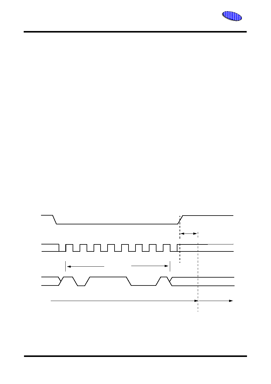
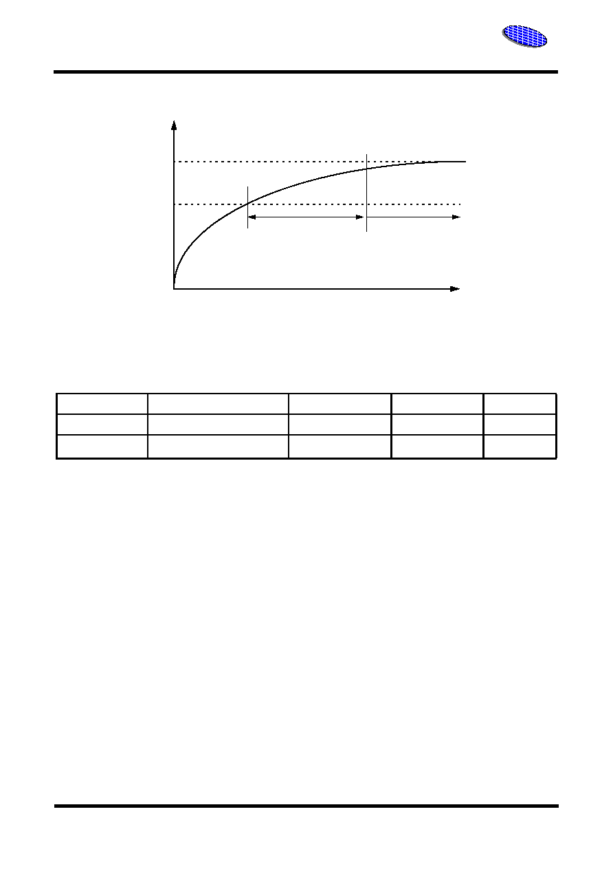
1) Vcc (min) at power-up, and then for a further
delay of t
PU
(as described in Table 5)
2) Vss at power-down
A simple pull-up resistor on Chip Select (CS#) can
usually be used to insure safe and proper power-up
and power-down.
The device ignores all instructions until a time delay
of t
PU
(as described in Table 5) has elapsed after the
moment that Vcc rises above the minimum Vcc
threshold. However, correct operation of the device
is not guaranteed if by this time Vcc is still below Vcc
(min). No Write Status Register, Program or Erase
instructions should be sent until t
PU
after Vcc
reaches the minimum Vcc threshold (See Figure
23).
At power-up, the device is in Standby mode (not
Deep Power Down mode) and the WEL bit is reset.
Normal precautions must be taken for supply rail
decoupling to stabilize the Vcc feed. Each device in
a system should have the Vcc rail decoupled by a
suitable capacitor close to the package pins (this
capacitor is generally of the order of 0.1uF).
At power-down, when Vcc drops from the operating
voltage to below the minimum Vcc threshold, all
operations are disabled and the device does not
respond to any instructions. (The designer needs to
be aware that if a power-down occurs while a Write,
Program or Erase cycle is in progress, data corrup-
tion can result.)
Erase Parameter Page(PE)
The Erase Parameter Page Instruction sets all 256
bytes of memory in the Parameter Page to the
erased state of all 1s (FFh). A Write Enable instruc-
tion must be executed before the device will accept
the Erase Parameter Page instruction(Status Regis-
ter bit WEL must equal 1). The instruction is initiated
by driving the CS# pin low and shifting the instruc-
tion code "D5h". The Erase Parameter Page instruc-
tion sequence is shown in Figure 22.
The CS# pin must be driven high after the eighth has
been latched. If this is not done the Erase Parameter
Page instruction will not be executed. After CS# is
driven high, the self-timed Erase Parameter Page
instuction will commence for a time duration of t
PE
.
While the Erase Parameter Page Cycle is in
progress, the Read Status Register instruction may
still be accessed to check the status of the WIP bit.
The WIP bit is a 1 during the Erase Parameter Page
cycel and becomes a 0 when finished and the device
is ready to accept other instructions again. After the
Erase Parameter Page cycle has started the Write
Enable Latch(WEL) bit in the Status Register is
cleared to 0. The Erase Parameter Page instruction
will not be executed if any page is protected by the
Block Protect(BP2, BP1, BP0) bits.
Power-up and Power-down
The device must not be selected at power-up or
power-down (that is, CS# must follow the voltage
applied on Vcc) until Vcc reaches the correct value
as follows:
1
1 0 1 0 1 0 1
0
1 2 3 4 5 6 7
Figure 22. Erase Parameter Page( PE ) Instruction Sequence
SCK
CS#
SI
Instruction
E S I
E S I
27
Rev. 0E May 11 , 2006
ES25P16
Excel Semiconductor inc.
ADVANCED INFORMATION
Figure 23. Power-Up Timing
Time
Vcc
Vcc
max
Vcc
min
Full Device Access
t
PU
Table 5. Power-Up Timing
Symbol
Parameter
Min.
Max.
Unit
Vcc (min)
Vcc (minimum)
2.7
V
t
PU
Vcc (min) to device operation
10
ms
Initial Delivery State
The device is delivered with all bits set to 1 (each
byte contains FFh). The Status Register contains
00h (all Status Register bits are 0).
Maximum Rating
Stressing the device above the rating listed in the
Absolute Maximum Ratings section below may
cause permanent damage to the device. Theses
are stress ratings only and operation of the device
at these or any other conditions above those indi-
cated in the Operating sections of this specification
is not implied. Exposure to Absolute Maximum Rat-
ing conditions for extended periods may affect
device reliability.
Absolute Maximum Ratings
Ambient Storage Temperature .... -65
o
C to +150
o
C
Voltage with Respect to Ground
All inputs and I/Os ........................... - 0.3V to 4.5V
Operating Ranges
Ambient Operating Temperature (T
A
)
Commercial .......................................... 0
o
C to +70
o
C
Industrial
.............................................. -40
o
C to +85
o
C
Positive Power Supply
Voltage Range ...........................................
2.7V to 3.6V
Note:Operating ranges define those limits between
which the functionality of the device is guaranteed
E S I
E S I
28
Rev. 0E May 11 , 2006
ES25P16
Excel Semiconductor inc.
ADVANCED INFORMATION
DC CHARACTERISTICS
This section summarizes the DC and AC Characteristics of the device. Designers should check that the oper-
ating conditions in their circuit match the measurement conditions specified in the Test Specifications in Table
7, when relying on the quoted parameters.
Symbol
Description
Test Conditions
Min.
Typ.
Max.
Unit
Vcc
Supply Voltage
2.7
3
3.6
V
I
LI
Input Leakage Current
V
IN
= GND to Vcc
1
uA
I
SB
Standby Current
CS# = Vcc
50
uA
I
DP
Deep Power Down Current
CS# = Vcc
1
10
uA
I
LO
Output Leakage Current
V
IN
= GND to Vcc
1
uA
I
CCI
Active Read Current
SCK = 0.1 Vcc / 0.9 Vcc
SO = Open
40MHz
6
mA
SCK = 0.1Vcc / 0.9 Vcc
SO= Open
75 MHz
12
I
CC2
Active Page Program Current
CS# = Vcc
24
mA
I
CC3
Active WRSR Current
CS# = Vcc
24
mA
I
CC4
Active Sector Erase Current
CS# = Vcc
24
mA
I
CC5
Active Bulk Erase Current
CS# = Vcc
24
mA
V
IL
Input Low Voltage
- 0.3
0.3 Vcc
V
V
IH
Input High Voltage
0.7 Vcc
Vcc + 0.5
V
V
OL
Output Low Voltage
I
OL
= 1.6 mA, Vcc = Vcc min
0.4
V
V
OH
Output High Voltage
I
OH
= -0.1mA,
Vcc - 0.2
V
Notes:
1. Typical values are at T
A
= 25
o
C and Vcc = 3V
Table.6 DC Characteristics
E S I
E S I
29
Rev. 0E May 11 , 2006
ES25P16
Excel Semiconductor inc.
ADVANCED INFORMATION
Symbol
Parameter
Min
Max
Unit
C
L
Load Capacitance
30
pF
Input Rise and Fall Times
5
ns
Input Pulse Voltage
0.2Vcc to 0.8Vcc
V
Input Timing Reference Voltage
0.3Vcc to 0.7Vcc
V
Output Timing Reference Voltage
0.5Vcc
V
Table 7. Test Specifications
Input and Output
Timing Reference levels
Input levels
0.8Vcc
0.2Vcc
0.5Vcc
Figure 24. AC Measurements I/O Waveform
0.3Vcc
0.7Vcc
TEST CONDITIONS

E S I
E S I
30
Rev. 0E May 11 , 2006
ES25P16
Excel Semiconductor inc.
ADVANCED INFORMATION
AC CHARACTERISTICS
Symbol
Description
Min
Typ
Max
Unit
F
SCK
SCK Clock Frequency READ instruction
D.C
40
MHz
F
SCK
SCK Clock Frequency for Fast Read
and all other instructions except Read
instruction
D.C
75
MHz
t
CRT
Clock Rise Time (Slew Rate)
0.1
V/ns
t
CFT
Clock Fall Time (Slew Rate)
0.1
V/ns
t
WH
SCK High Time
6
ns
t
WL
SCK Low Time
6
ns
t
CS
CS# High Time
100
ns
t
CSS
(Note 3)
CS# Setup Time
5
ns
t
CSH
(Note 3)
CS# Hold Time
5
ns
t
HD
(Note 3)
HOLD# Setup Time (relative to SCK)
5
ns
t
CD
(Note 3)
HOLD# Hold Time (relative to SCK)
5
ns
t
HC
HOLD# Setup Time (relative to SCK)
5
ns
t
CH
HOLD# Hold Time (relative to SCK)
5
ns
t
V
Output Valid
6
ns
t
HO
Output Hold Time
0
ns
t
HD:DAT
Data in Hold Time
3
ns
t
SU:DAT
Data in Setup Time
3
ns
t
R
Input Rise Time
5
ns
t
F
Input Fall Time
5
ns
t
LZ
(Note 3)
HOLD# to Output Low Z
6
ns
t
HZ
(Note 3)
HOLD# to Output High Z
6
ns
t
DIS
(Note 3)
Output Disable Time
8
ns
t
WPS
(Note 3)
Write Protect Setup Time
15
ns
t
WPH
(Note 3)
Write Protect Hold Time
15
ns
t
RES
Release DP Mode
3
us
t
DP
CS# High to Deep Power Down Mode
3
us
t
W
Write Status Register Time
5
ms
t
PP
Page Programming Time
1.5 (Note 1)
3 (Note 2)
ms
t
SE
Sector Erase Time
0.5 (Note 1)
3 (Note 2)
sec
t
BE
Bulk Erase Time
12 (Note 1)
24 (Note 2)
sec
t
PE
Parameter Page Erase Time
20
(Note 1)
100 (Note 2)
ms
Notes:
1. Typical program and erase times assume the following conditions : 25'C, Vcc = 3.0V ; 10,000 cycles ; checkerboard data pattern
2. Under worst-case conditions of 90'C ; Vcc = 2.7V ; 100,000 cycles.
3. Not 100% tested.
Table 8. AC Characteristics
E S I
E S I
31
Rev. 0E May 11 , 2006
ES25P16
Excel Semiconductor inc.
ADVANCED INFORMATION
Figure 25. SPI Mode 0
(0,0) Input Timing
SCK
CS#
SI
SO
Figure 26. SPI Mode 0 (0,0) Output Timing
LSB IN
t
CSS
t
CSH
t
CRT
t
HD:DAT
t
CSH
t
CSS
t
CS
MSB IN
t
CFT
t
SU:DAT
LSB OUT
t
DIS
t
WL
t
WH
t
V
t
HD
t
HD
t
V
SCK
CS#
SO

E S I
E S I
32
Rev. 0E May 11 , 2006
ES25P16
Excel Semiconductor inc.
ADVANCED INFORMATION
Figure 27. HOLD# Timing
SCK
CS#
SI
SO
t
CD
t
HC
t
HD
t
CH
t
LZ
t
HZ
HOLD#
High Impedance
SCK
CS#
SI
SO
W#
t
WPH
t
WPS
Figure 28. Write Protect Setup and Hold Timing during WRSR when SRWD = 1

E S I
E S I
33
Rev. 0E May 11 , 2006
ES25P16
Excel Semiconductor inc.
ADVANCED INFORMATION
PHYSICAL DIMENSIONS
S08 wide - 8 pin Plastic Small Outline 208 mils Body Width Package
b
c1
b1
(c)
WITH
PLATING
BASE
METAL
SECTION A-A
7
A
0.10 C
0.10 C
//
A2
A1
SEATING PLANE
C
SEATING
PLANE
GAUGE
PLANE
L
0.07 R MIN.
A
A
L1
SEE
DETAIL B
1
2
L2
C
H
DETAIL B
H
E
E/2
b
E1/2
E1
A
5
D
3
4
e
B
5
D
9
3
4
0.33 C
0.20 C
A-B
0.25 M C A-B D
NOTES:
1. All dimensions are in both inches and millimeters.
2. Dimensioning and tolerancing per ASME Y 14.5M - 1994.
3. Dimension D does not include mold flash, protrusions or gate burrs.
Mold flash, protrusions or gate burrs shall not exceed 0.15 mm per
end. Dimension E1 does not include interlead flash or protrusion
interlead flash or protrusion shall not exceed 0.25mm per side.
D and E1 dimensions are determined at datum H.
4. The package top may be smaller than the package bottom. Dime-
-nsions D and E1 are determined at the outmost extremes of the
plastic body exclusive of mold flash, tie bar burrs, gate burrs and
interlead flash. But including any mismatch between the top and
bottom of the plastic body.
5. Datums A and B to be determined at datum H.
6. "N" is the maximum number of terminal positions for the specified
package length H.
7. The dimensions apply to the flat section of the lead between 0.10 to
0.25 mm from the lead tip.
8. Dimension "b" does not include dambar protrusion. Allowable dam-
bar protrusion shall be 0.10 mm total in excess of the "b" dimension
at maximum material condition. The dambar cannot not be located
on the lower radius of the lead foot.
9. This chamfer feature is optional. If it is not present, then a pin 1
idenfifier must be located within the index area indicated.
10.Lead coplanarity shall be within 0.10 mm. As measured from the
seating plane.
Package
SOC 008 (inches)
SOC 008 (mm)
JEDEC
Symbol
MIN
MAX
MIN
MAX
A
0.069
0.085
1.753
2.159
A1
0.002
0.0098
0.051
0.249
A2
0.067
0.075
1.70
1.91
b
0.014
0.018
0.356
0.483
b1
0.013
0.018
0.330
0.457
c
0.0075
0.0095
0.191
0.241
c1
0.006
0.008
0.152
0.203
D
0.208 BSC
5.283 BSC
E
0.315 BSC
8.001 BSC
E1
0.208 BSC
5283 BSC
e
0.050 BSC
1.27 BSC
L
0.020
0.030
0.508
0.762
L1
0.055 REF
1.40 REF
L2
0.010 BSC
0.25 BSC
N
8
8
0'
8'
0'
8'
5'
15'
5'
15'
0'
0'
2
1

E S I
E S I
34
Rev. 0E May 11 , 2006
ES25P16
Excel Semiconductor inc.
ADVANCED INFORMATION
ORDERNG INFORMATION
Standard Products
ESI standard products are available in several package and operating ranges. The order number (Valid Combi-
nation) is formed by a combination of the following:
PACKAGE TYPE
2 : 8 pin 208 mil SOP
PACKAGE MATERIALS
C : Standard
G : Lead (Pb) - free (Note)
SPEED OPTION
75 : 75 Mhz
DENSITY
16 : 16 Mb
DEVICE FAMILY
ES25P : ESI Memory 3.0 Volt-only, Serial Peripheral
Interface (SPI) Flash Memory
ES25P 16 - 75 C G 2 T
PACKING TYPE
T : Tube (standard) (Note)
R : 13" Tape and Reel (Note)
Y : Tray
TEMPERATURE RANGE
I : Industrial (- 40
o
C to + 85
o
C)
C : Commercial ( 0
o
C to + 70
o
C)
Table 1. ES25P Valid Combinations
ES25P Valid Combinations
Base Ordering
Part Number
Speed Option
Temperature &
Package Material
Package Type
Packing Type
Package Marking
ES25P16
75
CG, CC, IG,IC
(Note)
2, 7
T, R,Y
(Note)
P16 + (Speed) + (Temp)
+(
Package Material
)
Notes:
Contact your local sales office for availability.

E S I
E S I
35
Rev. 0E May 11 , 2006
ES25P16
Excel Semiconductor inc.
ADVANCED INFORMATION
Excel Semiconductor Inc.
1010 Keumkang Hightech Valley, Sangdaewon1-Dong 133-1, Jungwon-Gu, Seongnam-Si, Kyongki-Do, Rep.
of Korea.
Zip Code : 462-807 Tel : +82-31-777-5060 Fax : +82-31-740-3798
/ Homepage : www.excelsemi.com
The
attached
datasheets
are
provided by Excel Semiconductor.inc (ESI). ESI
reserves
the
right
to change the spec-
ifications and products. ESI will answer to your questions about device. If you have any questions, please
contact the
ESI office.
Document Title
16M Serial Flash Memory
Revision History
Revision Number
Data
Items
Rev. 0A
JUN. 27,2005
Initial Release Version.
Rev.0B
JAN. 18,2006
Added Parameter Page data to Features, and Read Manufac-
turer ID & Device ID
Rev.0C
Mar. 14, 2006
Device Name Changed
Rev.0D
May. 01, 2006
The Clock Frequency was changed from 66MHz to 75MHz
Rev.0E
May.11, 2006
WSON package not supported