
E S I
E S I
1
Rev. 2D Jan 5, 2006
ES29LV320D
Excel Semiconductor inc.
ES29LV320D
32Mbit(4M x 8/2M x 16)
CMOS 3.0 Volt-only, Boot Sector Flash Memory
GENERAL FEATURES
∑ Single power supply operation
- 2.7V -3.6V for read, program and erase operations
∑ Sector Structure
- 8Kbyte x 8 boot sectors
- 64Kbyte x 63 sectors
- 256byte security sector
∑ Top or Bottom boot block
- ES29LV320DT for Top boot block device
- ES29LV320DB for Bottom boot block device
∑ A 256 bytes of extra sector for security code
- Factory lockable
- Customer lockable
∑ Package Options
- 48-pin TSOP
- Pb-free packages
- All Pb-free products are RoHS-Compliant
∑ Low Vcc write inhibit
∑ Manufactured on 0.18um process technology
∑ Compatible with JEDEC standards
- Pinout and software compatible with single-power
supply flash standard
DEVICE PERFORMANCE
∑ Read access time
- 90ns/120n for normal Vcc range ( 2.7V - 3.6V )
- 80ns for regulated Vcc range ( 3.0V - 3.6V )
∑ Program and erase time
- Program time : 9us/byte, 11us/word ( typical )
- Accelerated program time : 8us/word ( typical )
- Sector erase time : 0.7sec/sector ( typical )
∑ Power consumption (typical values)
- 200nA in standby or automatic sleep mode
- 10 mA active read current at 5 MHz
- 15mA active write current during program or erase
∑ Minimum 100,000 program/erase cycles per sector
∑ 20 Year data retention at
125
o
C
SOFTWARE FEATURES
∑ Erase Suspend / Erase Resume
∑ Data# poll and toggle for Program/erase status
∑ CFI ( Common Flash Interface) supported
∑ Unlock Bypass program
∑ Autoselect mode
∑ Auto-sleep mode after t
ACC
+ 30ns
HARDWARE FEATURES
∑ Hardware reset input pin ( RESET#)
- Provides a hardware reset to device
- Any internal device operation is terminated and the
device returns to read mode by the reset
∑ Ready/Busy# output pin ( RY/BY#)
- Provides a program or erase operational status
about whether it is finished for read or still being
progressed
∑ WP#/ACC input pin
- Two outermost boot sectors are protected when
WP# is set to low, regardless of sector protection
- Program speed is accelerated by raising WP#/ACC
to a high voltage (12V)
∑ Sector protection / unprotection ( RESET# , A9 )
- Hardware method of locking a sector to prevent
any program or erase operation within that sector
- Two methods are provided :
- In-system method by RESET# pin
- A9 high-voltage method for PROM programmers
∑ Temporary Sector Unprotection ( RESET# )
- Allows temporary unprotection of previously
protected sectors to change data in-system

E S I
E S I
2
Rev. 2D Jan 5, 2006
ES29LV320D
Excel Semiconductor inc.
The ES29LV320 is a 32 megabit, 3.0 volt-only flash
memory device, organized as 4M x 8 bits (Byte
mode) or 2M x 16 bits (Word mode) which is config-
urable by BYTE#. Eight boot sectors and sixty three
main sectors with uniform size are provided :
8Kbytes x 8 and 64Kbytes x 63. The device is man-
ufactured with ESI's proprietary, high performance
and highly reliable 0.18um CMOS flash technology.
The device can be programmed or erased in-sys-
tem with standard 3.0 Volt Vcc supply ( 2.7V-3.6V)
and can also be programmed in standard EPROM
programmers. The device offers minimum endur-
ance of 100,000 program/erase cycles and more
than 10 years of data retention.
The ES29LV320 offers access time as fast as 80ns
or 90ns, allowing operation of high-speed micropro-
cessors without wait states. Three separate control
pins are provided to eliminate bus contention : chip
enable (CE#), write enable (WE#) and output
enable (OE#).
All program and erase operation are automatically
and internally performed and controlled by embed-
ded program/erase algorithms built in the device.
The device automatically generates and times the
necessary high-voltage pulses to be applied to the
cells, performs the verification, and counts the num-
ber of sequences. Some status bits (DQ7, DQ6 and
DQ5) read by data# polling or toggling between
consecutive read cycles provide to the users the
internal status of program/erase operation: whether
it is successfully done or still being progressed.
Extra Security Sector of 256 bytes
In the device, an extra security sector of 256 bytes is
provided to customers. This extra sector can be
used for various purposes such as storing ESN
(Electronic Serial Number) or customer's security
codes. Once after the extra sector is written, it can
be permanently locked by the device manufacturer(
factory-locked) or a customer( customer-lock-
able). At the same time, a lock indicator bit (DQ7)
is permanently set to a 1 if the part is factory- locked,
or set to 0 if it is customer-lockable. Therefore, this
lock indicator bit (DQ7) can be properly used to
avoid that any customer-lockable part is used to
replace a factory-locked part. The extra security
sector is an extra memory space for customers
when it is used as a customer-lockable version. So,
it can be read and written like any other sectors. But
it should be noted that the number of E/W(Erase and
Write) cycles is limited to 300 times (maximum) only
in the Security Sector.
Special services such as ESN and factory-lock are
available to customers ( ESI's Special-Code ser-
vice ) The ES29LV320 is completely compatible with
the JEDEC standard command set of single power
supply Flash. Commands are written to the internal
command register using standard write timings of
microprocessor and data can be read out from the
cell array in the device with the same way as used in
other EPROM or flash devices.
GENERAL PRODUCT DESCRIPTION
E S I
E S I
3
Rev. 2D Jan 5, 2006
ES29LV320D
Excel Semiconductor inc.
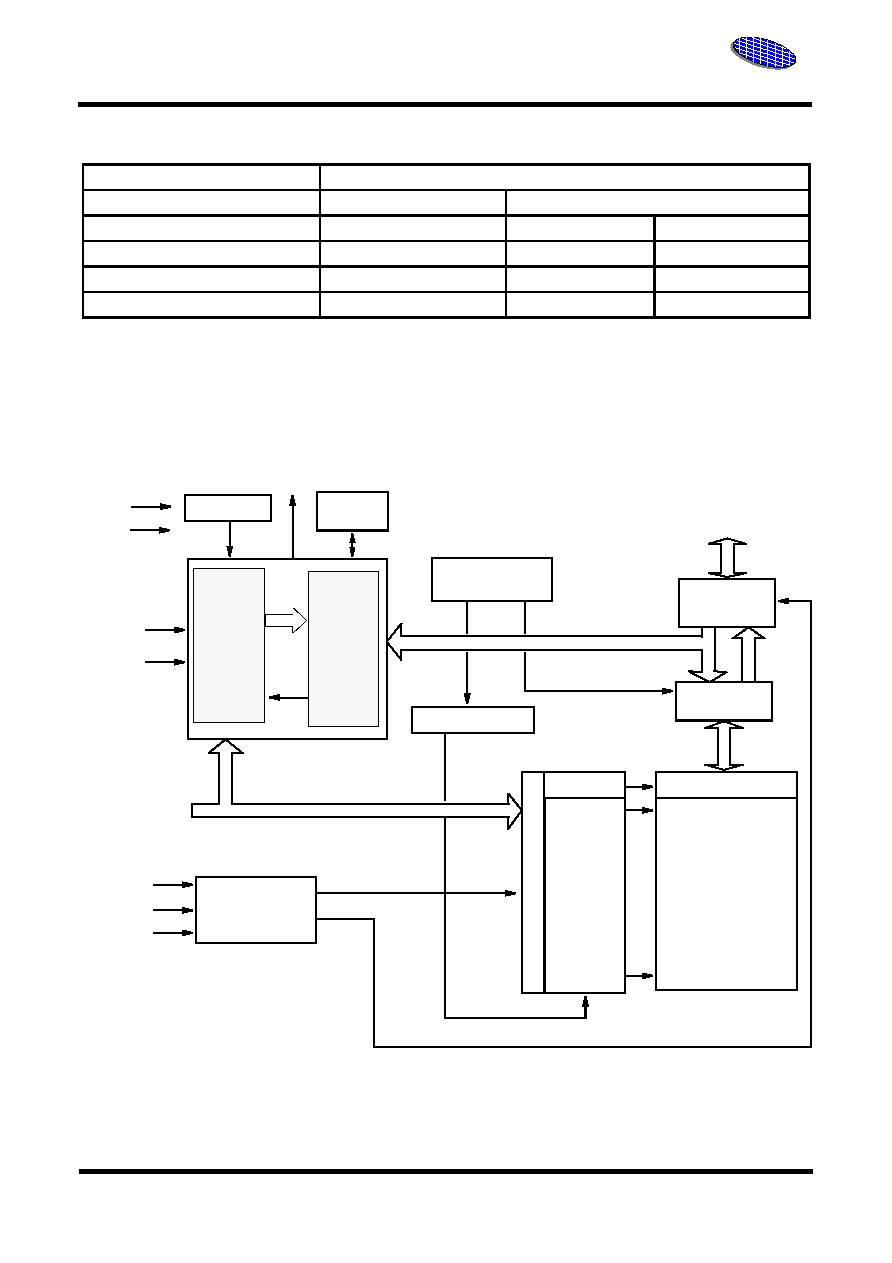
PRODUCT SELECTOR GUIDE
Family Part Number
ES29LV320
Voltage Range
3.0 ~ 3.6V
2.7 ~ 3.6V
Speed Option
80R
90
120
Max Access Time (ns)
80
90
120
CE# Access (ns)
80
90
120
OE# Access (ns)
35
40
50
Command
Register
Analog Bias
Generator
Add
r
e
ss Latch
BYTE#
CE#
OE#
A<0:20
>
RESET#
Vcc
Vss
Chip Enable
Output Enable
Logic
Vcc Detector
Timer/
Counter
Y-Decoder
X-Decoder
Y-Decoder
Cell Array
Data Latch/
Sense Amps
Input/Output
Buffers
Sector Switches
DQ0-DQ15(A-1)
RY/BY#
Write
State
Machine
WE
#
FUNCTION BLOCK DIAGRAM
E S I
E S I
4
Rev. 2D Jan 5, 2006
ES29LV320D
Excel Semiconductor inc.
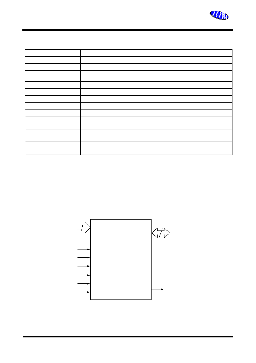
PIN DESCRIPTION
Pin
Description
A0-A20
21 Addresses
DQ0-DQ14
15 Data Inputs/Outputs
DQ15/A-1
DQ15 (Data Input/Output, Word Mode)
A-1 (LSB Address Input, Byte Mode)
CE#
Chip Enable
OE#
Output Enable
WE#
Write Enable
WP#/ACC
Hardware Write Protect/Acceleration Pin
RESET#
Hardware Reset Pin, Active Low
BYTE#
Selects 8-bit or 16-bit mode
RY/BY#
Ready/Busy Output
Vcc
3.0 volt-only single power supply
(see Product Selector Guide for speed options and voltage supply tolerances)
Vss
Device Ground
NC
Pin Not Connected Internally
LOGIC SYMBOL
DQ0 ~ DQ15
(A-1)
RY/BY#
BYTE#
RESET#
OE#
CE#
A0 ~ A20
WP#/ACC
WE#
21
16 or 8

E S I
E S I
5
Rev. 2D Jan 5, 2006
ES29LV320D
Excel Semiconductor inc.
CONNECTION DIAGRAM
A15
A14
A13
A12
A11
A10
A9
A8
A19
A20
WE#
RESET#
NC
WP#/ACC
RY/BY#
A18
A17
A7
A6
A5
A4
A3
A2
A1
A16
BYTE#
Vss
DQ15/A-1
DQ7
DQ14
DQ6
DQ13
DQ5
DQ12
DQ4
Vcc
DQ11
DQ3
DQ10
DQ2
DQ9
DQ1
DQ8
DQ0
OE#
Vss
CE#
A0
1
2
3
4
5
6
7
8
9
10
11
12
13
14
15
16
17
18
19
20
21
22
23
24
48
47
46
45
44
43
42
41
40
39
38
37
36
35
34
33
32
31
30
29
28
27
26
25
48-Pin Standard TSOP
ES29LV320