 | –≠–ª–µ–∫—Ç—Ä–æ–Ω–Ω—ã–π –∫–æ–º–ø–æ–Ω–µ–Ω—Ç: FT0405DE | –°–∫–∞—á–∞—Ç—å:  PDF PDF  ZIP ZIP |
On-State Current
4 Amp
FT04...E/F
LOGIC LEVEL TRIAC
Absolute Maximum Ratings, according to IEC publication No. 134
Gate Trigger Current
< 5 mA to < 10 mA
Off-State Voltage
200 V ˜ 600 V
Jul - 02
Repetitive Peak Off State
Voltage
PARAMETER
CONDITIONS
VOLTAGE
Unit
SYMBOL
V
DRM
V
RRM
R
GK
= 1 K
B
200
V
D
400
M
600
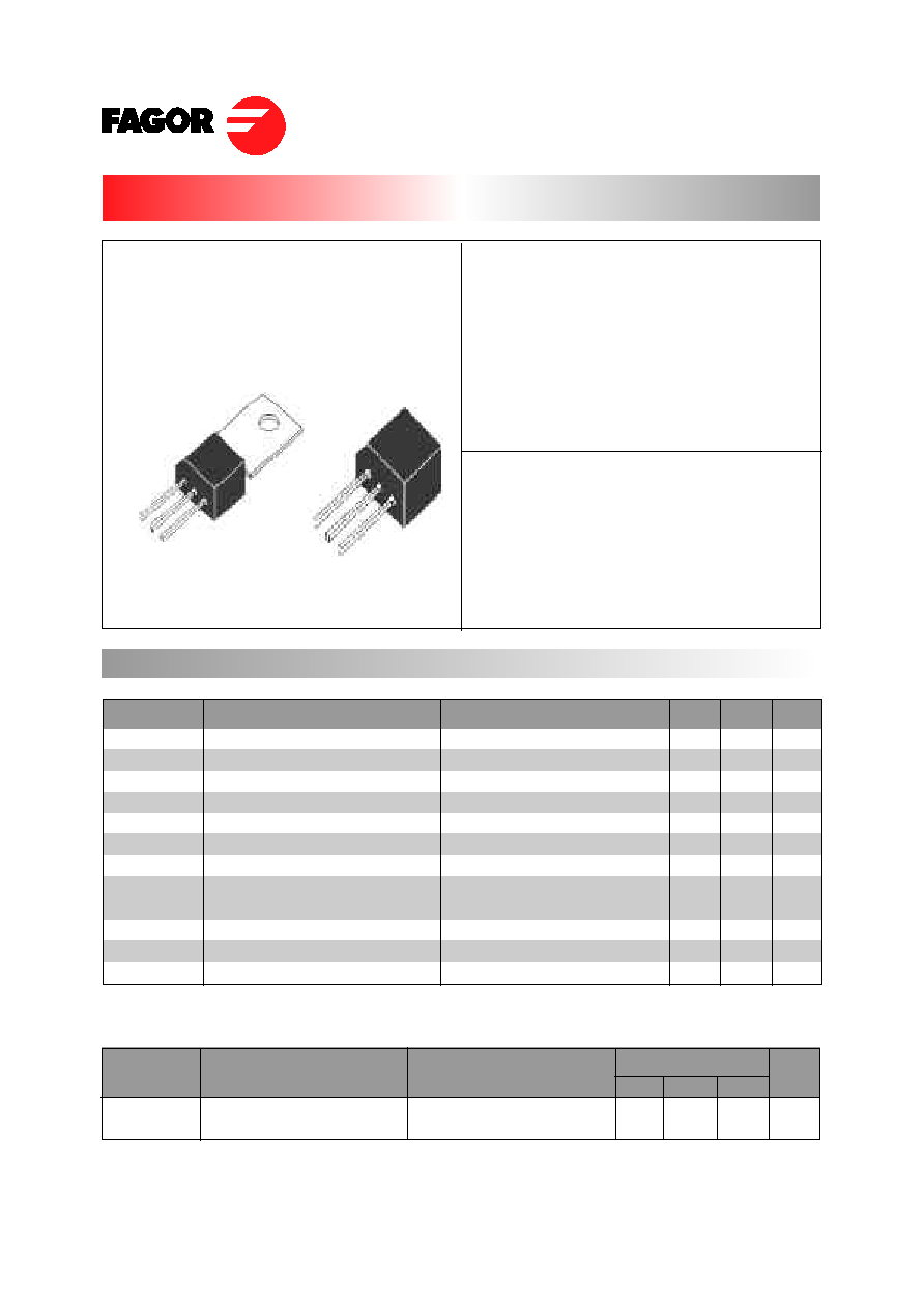
TO202-1 (E)
MT1
MT2
G
MT2
TO202-3 (F)
MT1
MT2
G
MT2
RMS On-state Current
Non-repetitive On-State Current
Non-repetitive On-State Current
Fusing Current
Peak Gate Current
Peak Gate Dissipation
Gate Dissipation
Critical rate of rise of on-state current
Operating Temperature
Storage Temperature
Soldering Temperature
I
T(RMS)
PARAMETER
CONDITIONS
Min.
Max.
Unit
SYMBOL
I
TSM
I
TSM
I
2
t
I
GM
P
GM
P
G(AV)
T
j
T
stg
T
sld
All Conduction Angle, T
c
= 110 ∫C
Half Cycle, 60 Hz
Half Cycle, 50 Hz
t
p
= 10 ms, Half Cycle
20 µs max.
20 µs max.
20 ms max.
1.6 mm from case, 10s max.
4
21
20
2.2
20
-40
-40
A
A
A
A
2
s
A
W
W
A/µs
∫C
∫C
∫C
1.2
2
0.2
+125
+150
260
di/dt
Tr
200 ns, F = 120 Hz
T
j
= 125 ∫C
I
G
= 2 x I
GT
This series of TRIACs uses a high
performance PNPN technology.
These parts are intended for general
purpose AC switching applications with
highly inductive loads.

FT04...E/F
LOGIC LEVEL TRIAC
PART NUMBER INFORMATION
Jul - 02
FAGOR
SCR
CURRENT
CASE
VOLTAGE
SENSITIVITY
F
T
04
09
B
E
00
FORMING
TU
PACKAGING
Electrical Characteristics
Gate Trigger Current
Off-State Leakage Current
Threshold Voltage
Dynamic Resistance
On-state Voltage
Gate Trigger Voltage
Gate Non Trigger Voltage
Holding Current
Latching Current
Critical Rate of Voltage Rise
PARAMETER
CONDITIONS
SENSITIVITY
Unit
SYMBOL
I
GT
I
DRM
V
D
= 12 V
DC
, R
L
= 30
, T
j
= 25 ∫C
mA
mA
0.5
5
0.95
180
2
1.3
0.2
15
100
mA
µA
V
m
V
V
V
mA
mA
V/µs
V/µs
MAX
MAX
MAX
MAX
MAX
MAX
MAX
MAX
MIN
MAX
MAX
MAX
MIN
MIN
/I
RRM
V
TM
*
V
GT
V
GD
I
H
*
I
L
dv / dt*
R
th(j-a)
Thermal Resistance
Junction-Ambient
V
D
= V
DRM
,
T
j
= 125 ∫C
T
j
= 25 ∫C
V
R
= V
RRM
,
I
T
= 5.5 Amp, tp = 380 µs, T
j
= 25 ∫C
V
D
= 12 V
DC
, R
L
= 30
, T
j
= 25 ∫C
I
T
= 50 mA
T
j
= 25 ∫C
I
G
= 1.2 I
GT
,
T
j
= 25 ∫C
V
D
= 0.67 x V
DRM
, Gate open
T
j
= 125 ∫C
Quadrant
Q1˜Q3
Q4
Q1˜Q4
Q1˜Q4
Q1,Q3,Q4
Q2
V
D
= V
DRM
, R
L
= 3.3K
, T
j
= 125 ∫C
∫C/W
∫C/W
(*) For either polarity of electrode MT2 voltage with reference to electrode MT1.
R
th(j-l)
Thermal Resistance
Junction-Leads for AC
(dv/dt)c*
(di/dt)c= 1.8 A/ms T
j
= 110 ∫C
V
to
R
d
T
j
= 125 ∫C
T
j
= 125 ∫C
05
5
5
09
10
10
10
15
25
100
2
7
10
15
20
1
Critidal rise rate of
commutating off-state
Voltage
FT04...E/F
LOGIC LEVEL TRIAC
Jul - 02
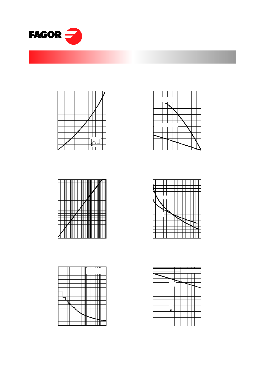
Fig. 1: Maximum average power disipation
versus RMS on-state current (full cycle)
0
2
5
4
3
2
1
0
P (W)
IT(RMS)(A)
0.5
3
360 ∫
Fig. 2: RMS on-state current versus ambient
temperature (full cycle)
I T(RMS) (A)
T amb (∫C)
5
4
3
2
1
0
0
25
50
75
100
125
1
1.5
2.5
3.5
Fig. 3: Relative variation of thermal impedance
junction to ambient versus pulse duration.
IGT, IH, IL (Tj) / IGT, IH, IL (Tj = 25 ∫C)
Fig. 4: Relative variation of gate trigger
current, holding and latching current versus
junction temperature.
Tj (∫C)
2.5
2.0
1.5
1.0
0.5
0.0
-40 -20
20
60
80 100
0
40
120 140
IH & IL
IGT
ITSM(A). I
2
t (A
2
s)
Fig. 6: Non repetitive surge peak on-state
current for a sinusoidal pulse with width:
tp
10 ms, and corresponding value of I
2
t.
100
10
1
1
10
Tj initial = 25 ∫C
tp(ms)
ITSM
I
2
t
1
10
100
1000
Fig. 5: Non repetitive surge peak on-state
current versus number of cycles.
35
30
25
20
15
10
5
0
I TSM (A)
Number of cycles
Tj initial = 25 ∫C
F= 50Hz
Rth(j-a)=100 ∫C/W
1.00
0.10
0.01
Zth(j-a) / Rth(j-a)
1E-3
1E-2
1E-1
1E+0
1E+1
1E+2 5E+2
tp (s)
Rth(j-a)=Rth(j-l)

FT04...E/F
Jul - 02
LOGIC LEVEL TRIAC
Fig. 7: On-state characteristics (maximum
values)
20.0
1.0
0.1
ITM(A)
0
0.5 1 1.5
2 2.5 3 3.5 4 4.5
Tj initial
25 ∫C
VTM(V)
Tj max
Vto = 0.95 V
Rd = 180 mW
(.287)
7,3
C
D
10,5
(.413)
N1
2,54
(.100)
P
5,3
N
(.209)
max.
O
max.
max.
1,4
(.055)
(.028)
0,7
TO 202-3
A
max.
10,1
(.398)
1,5
(.059)
max.
F
M
4,5
(.177)
H
(.020)
0,51
J
1,5
(.059)
3,16
3,20
(.124)
(.126)
K
(.126)
3,2
A
max.
10,1
(.398)
G
J
H
1,5
(.059)
(.020)
0,51
M
13,7
(.540)
(.287)
7,3
C
D
10,5
(.413)
N1
2,54
(.100)
P
5,3
N
(.209)
max.
O
I
max.
max.
1,4
(.055)
(.028)
0,7
4,5
(.177)
TO 202-1
1,5
(.059)
max.
F
PACKAGE MECHANICAL DATA
TO 202-1
TO 202-3
10.0
Tj max