 | –≠–ª–µ–∫—Ç—Ä–æ–Ω–Ω—ã–π –∫–æ–º–ø–æ–Ω–µ–Ω—Ç: 100304QC | –°–∫–∞—á–∞—Ç—å:  PDF PDF  ZIP ZIP |
© 2000 Fairchild Semiconductor Corporation
DS010581
www.fairchildsemi.com
August 1989
Revised August 2000
1
00304 Low
Power Quint
AND/NAND G
a
t
e
100304
Low Power Quint AND/NAND Gate
General Description
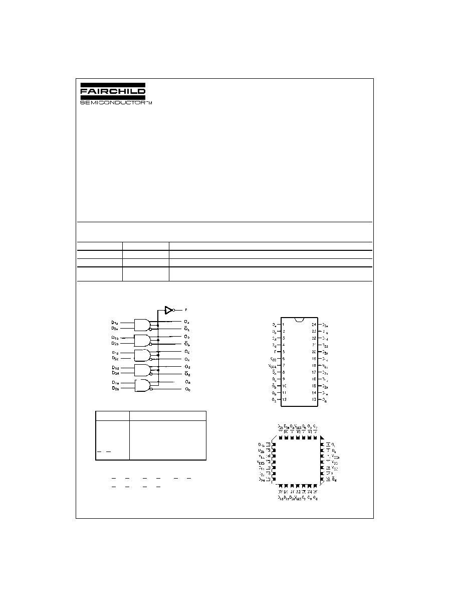
The 100304 is monolithic quint AND/NAND gate. The
Function output is the wire-NOR of all five AND gate out-
puts. All inputs have 50 k
pull-down resistors.
Features
s
Low Power Operation
s
2000V ESD protection
s
Pin/function compatible with 100104
s
Voltage compensated operating range
=
-
4.2V to
-
5.7V
s
Available to industrial grade temperature range
(PLCC package only)
Ordering Code:
Devices also available in Tape and Reel. Specify by appending the suffix letter "X" to the ordering code.
Logic Symbol
Pin Descriptions
Logic Equation
Connection Diagrams
24-Pin DIP
28-Pin PLCC
Order Number
Package Number
Package Description
100304PC
N24E
24-Lead Plastic Dual-In-Line Package (PDIP), JEDEC MS-010, 0.400 Wide
100304QC
V28A
28-Lead Plastic Lead Chip Carrier (PLCC), JEDEC MO-047, 0.450 Square
100304QI
V28A
28-Lead Plastic Lead Chip Carrier (PLCC), JEDEC MO-047, 0.450 Square
Industrial Temperature Range (
-
40
∞
C to
+
85
∞
C)
Pin Names
Description
D
na
≠D
ne
Data Inputs
F
Function Output
O
a
≠O
e
Data Outputs
O
a
≠O
e
Complementary Data Outputs
F
=
(D
1a
∑ D
2a
)
+
(D
1b
∑ D
2b
)
+
(D
1c
∑ D
2c
)
+
(D
1d
∑ D
2d
)
+
(D
1e
∑ D
2e
).
www.fairchildsemi.com
2
100304
Absolute Maximum Ratings
(Note 1)
Recommended Operating
Conditions
Note 1: The "Absolute Maximum Ratings" are those values beyond which
the safety of the device cannot be guaranteed. The device should not be
operated at these limits. The parametric values defined in the Electrical
Characteristics tables are not guaranteed at the absolute maximum rating.
The "Recommended Operating Conditions" table will define the conditions
for actual device operation.
Note 2: ESD testing conforms to MIL-STD-883, Method 3015.
Commercial Version
DC Electrical Characteristics
(Note 3)
V
EE
=
-
4.2V to
-
5.7V, V
CC
=
V
CCA
=
GND, T
C
=
0
∞
C to
+
85
∞
C
Note 3: The specified limits represent the "worst case" value for the parameter. Since these values normally occur at the temperature extremes, additional
noise immunity and guardbanding can be achieved by decreasing the allowable system operating ranges. Conditions for testing shown in the tables are cho-
sen to guarantee operation under "worst case" conditions.
DIP AC Electrical Characteristics
V
EE
=
-
4.2V to
-
5.7V, V
CC
=
V
CCA
=
GND
PLCC AC Electrical Characteristics
V
EE
=
-
4.2V to
-
5.7V, V
CC
=
V
CCA
=
GND
Storage Temperature (T
STG
)
-
65
∞
C to
+
150
∞
C
Maximum Junction Temperature (T
J
)
+
150
∞
C
V
EE
Pin Potential to Ground Pin
-
7.0V to
+
0.5V
Input Voltage (DC)
V
EE
to
+
0.5V
Output Current (DC Output HIGH)
-
50 mA
ESD (Note 2)
2000V
Case Temperature (T
C
)
Commercial
0
∞
C to
+
85
∞
C
Industrial
-
40
∞
C to
+
85
∞
C
Supply Voltage (V
EE
)
-
5.7V to
-
4.2V
Symbol
Parameter
Min
Typ
Max
Units
Conditions
V
OH
Output HIGH Voltage
-
1025
-
955
-
870
mV
V
IN
=
V
IH (Max)
Loading with
V
OL
Output LOW Voltage
-
1830
-
1705
-
1620
mV
or V
IL (Min)
50
to
-
2.0V
V
OHC
Output HIGH Voltage
-
1035
mV
V
IN
=
V
IH(Min)
Loading with
V
OLC
Output LOW Voltage
-
1610
mV
or V
IL (Max)
50
to
-
2.0V
V
IH
Input HIGH Voltage
-
1165
-
870
mV
Guaranteed HIGH Signal
for All Inputs
V
IL
Input LOW Voltage
-
1830
-
1475
mV
Guaranteed LOW Signal
for All Inputs
I
IL
Input LOW Current
0.50
µ
A
V
IN
=
V
IL (Min)
I
IH
Input High Current
D
2a
≠D
2e
250
µ
A
V
IN
=
V
IH
(Max)
D
1a
≠D
1e
350
I
EE
Power Supply Current
-
69
-
43
-
30
mA
Inputs open
Symbol
Parameter
T
C
=
0
∞
C
T
C
=
+
25
∞
C
T
C
=
+
85
∞
C
Units
Conditions
Min
Max
Min
Max
Min
Max
t
PLH
Propagation Delay
0.40
1.75
0.40
1.65
0.40
1.75
ns
t
PHL
D
na
≠D
ne
to O, O
Figures 1, 2
t
PLH
Propagation Delay
1.00
2.60
1.00
2.60
1.15
3.20
ns
t
PHL
Data to F
t
TLH
Transition Time
0.35
1.20
0.35
1.20
0.35
1.20
ns
t
THL
20% to 80%, 80% to 20%
Symbol
Parameter
T
C
=
0
∞
C
T
C
=
+
25
∞
C
T
C
=
+
85
∞
C
Units
Conditions
Min
Max
Min
Max
Min
Max
t
PLH
Propagation Delay
0.40
1.55
0.40
1.45
0.40
1.55
ns
t
PHL
D
na
≠D
ne
to O, O
Figures 1, 2
t
PLH
Propagation Delay
1.00
2.40
1.00
2.40
1.15
3.00
ns
t
PHL
Data to F
t
TLH
Transition Time
0.35
1.10
0.35
1.15
0.35
1.10
ns
t
THL
20% to 80%, 80% to 20%
3
www.fairchildsemi.com
1
00304
Industrial Version
PLCC DC Electrical Characteristics
(Note 4)
V
EE
=
-
4.2V to
-
5.7V, V
CC
=
V
CCA
=
GND, T
C
=
-
40
∞
C to
+
85
∞
C
Note 4: The specified limits represent the "worst case" value for the parameter. Since these values normally occur at the temperature extremes, additional
noise immunity and guardbanding can be achieved by decreasing the allowable system operating ranges. Conditions for testing shown in the tables are cho-
sen to guarantee operation under "worst case" conditions.
PLCC AC Electrical Characteristics
V
EE
=
-
4.2V to
-
5.7V, V
CC
=
V
CCA
=
GND
Symbol
Parameter
T
C
=
-
40
∞
C
T
C
=
0
∞
C to
+
85
∞
C
Units
Conditions
Min
Max
Min
Max
V
OH
Output HIGH Voltage
-
1085
-
870
-
1025
-
870
mV
V
IN
=
V
IH (Max)
Loading with
V
OL
Output LOW Voltage
-
1830
-
1575
-
1830
-
1620
or V
IL (Min)
50
to
-
2.0V
V
OHC
Output HIGH Voltage
-
1095
-
1035
mV
V
IN
=
V
IH(Min)
Loading with
V
OLC
Output LOW Voltage
-
1565
-
1610
or V
IL (Max)
50
to
-
2.0V
V
IH
Input HIGH Voltage
-
1170
-
870
-
1165
-
870
mV
Guaranteed HIGH Signal
for All Inputs
V
IL
Input LOW Voltage
-
1830
-
1480
-
1830
-
1475
mV
Guaranteed LOW Signal
for All Inputs
I
IL
Input LOW Current
0.50
0.50
µ
A
V
IN
=
V
IL (Min)
I
IH
Input HIGH Current
D
2a
≠D
2e
250
250
µ
A
V
IN
=
V
IH (Max)
D
1a
≠D
1e
350
350
I
EE
Power Supply Current
-
69
-
30
-
69
-
30
mA
Inputs OPEN
Symbol
Parameter
T
C
=
40
∞
C
T
C
=
+
25
∞
C
T
C
=
+
85
∞
C
Units
Conditions
Min
Max
Min
Max
Min
Max
t
PLH
Propagation Delay
0.35
1.55
0.40
1.45
0.40
1.55
ns
Figures 1, 2
t
PHL
D
na
≠D
ne
to O, O
t
PLH
Propagation Delay
1.00
2.40
1.00
2.40
1.15
3.00
ns
t
PHL
Data to F
t
TLH
Transition Time
0.35
1.10
0.35
1.15
0.35
1.10
ns
t
THL
20% to 80%, 80% to 20%
www.fairchildsemi.com
4
100304
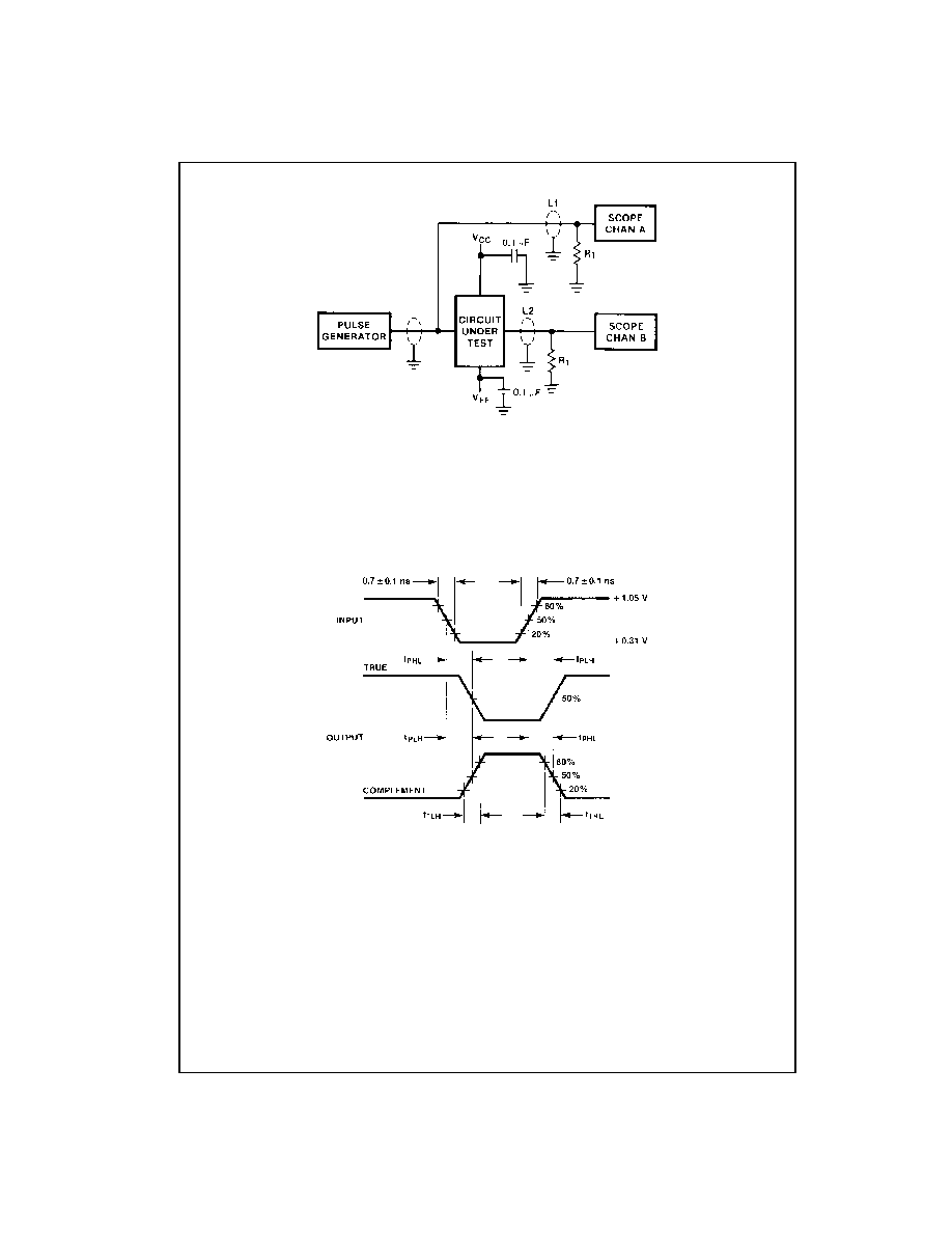
Test Circuitry
Notes:
V
CC
, V
CCA
=
+
2V, V
EE
=
-
2.5V
L1 and L2
=
equal length 50
impedance lines
R
T
=
50
terminator internal to scope
Decoupling 0.1
µ
F from GND to V
CC
and V
EE
All unused outputs are loaded with 50
to GND
C
L
=
Fixture and stray capacitance
3 pF
FIGURE 1. AC Test Circuit
Switching Waveforms
FIGURE 2. Propagation Delay and Transition Times
5
www.fairchildsemi.com
1
00304
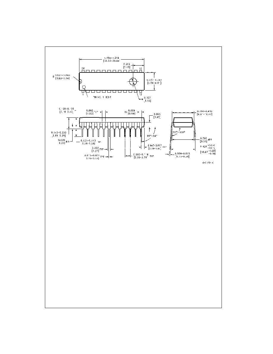
Physical Dimensions
inches (millimeters) unless otherwise noted
24-Lead Plastic Dual-In-Line Package (PDIP), JEDEC MS-010, 0.400 Wide
Package Number N24E