 | –≠–ª–µ–∫—Ç—Ä–æ–Ω–Ω—ã–π –∫–æ–º–ø–æ–Ω–µ–Ω—Ç: 100319QC | –°–∫–∞—á–∞—Ç—å:  PDF PDF  ZIP ZIP |
© 1999 Fairchild Semiconductor Corporation
DS010923
www.fairchildsemi.com
May 1991
Revised November 1999
1
00319 Low
Power Hex
Li
ne Dri
ver w
i
th
Cut
-
Off
100319
Low Power Hex Line Driver with Cut-Off
General Description
The 100319 is a Hex Line Driver with output cut-off capabil-
ity. The 100319 has single ended ECL inputs and differen-
tial ECL outputs, designed to drive a differential, doubly
terminated 50
transmission line (25
equivalent imped-
ance) in an ECL backplane. A LOW on the Output Enable
(OE) will set both the true and complementary outputs, to a
high impedance or cut-off state. The cut-off state is
designed to be more negative than a normal ECL LOW
state.
Features
s
Differential outputs
s
Output cut-off capability
s
Drives a 25
ECL load
s
2000V ESD protection
s
Voltage compensated range
=
-
4.2V to
-
5.7V
s
Available to industrial grade temperature range
Ordering Code:
Devices also available in Tape and Reel. Specify by appending the suffix letter "X" to the ordering code.
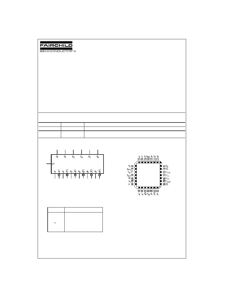
Logic Symbol
Pin Descriptions
Connection Diagram
28-Pin PLCC
Order Number
Package Number
Package Description
100319QC
V28A
28-Lead Plastic Lead Chip Carrier (PLCC), JEDEC MO-047, 0.450 Square
100319QI
V28A
28-Lead Plastic Lead Chip Carrier (PLCC), JEDEC MO-047, 0.450 Square
Industrial Temperature Range (
-
40
∞
C to
+
85
∞
C)
Pin Names
Description
D
n
Data Inputs
Q
n
Data Outputs
Q
n
Complementary Data Outputs
OE
Output Enable
www.fairchildsemi.com
2
100319
Truth Table
H
=
HIGH Voltage Level
L
=
LOW Voltage Level
X
=
Don't Care
Cut-off
=
Lower-than-LOW State
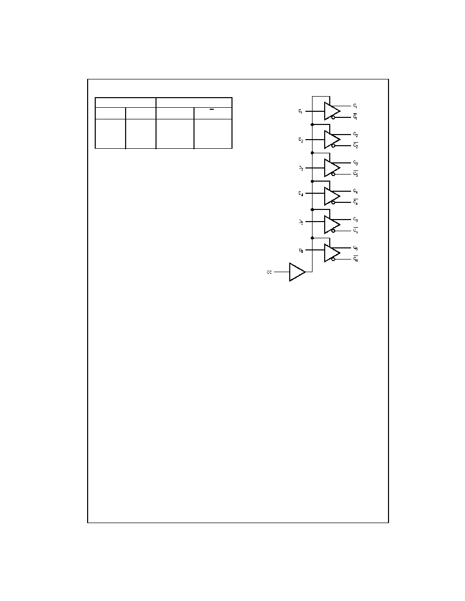
Logic Diagram
Inputs
Outputs
D
n
OE
Q
n
Q
n
L
H
L
H
H
H
H
L
X
L
Cut-Off
Cut-Off
3
www.fairchildsemi.com
1
00319
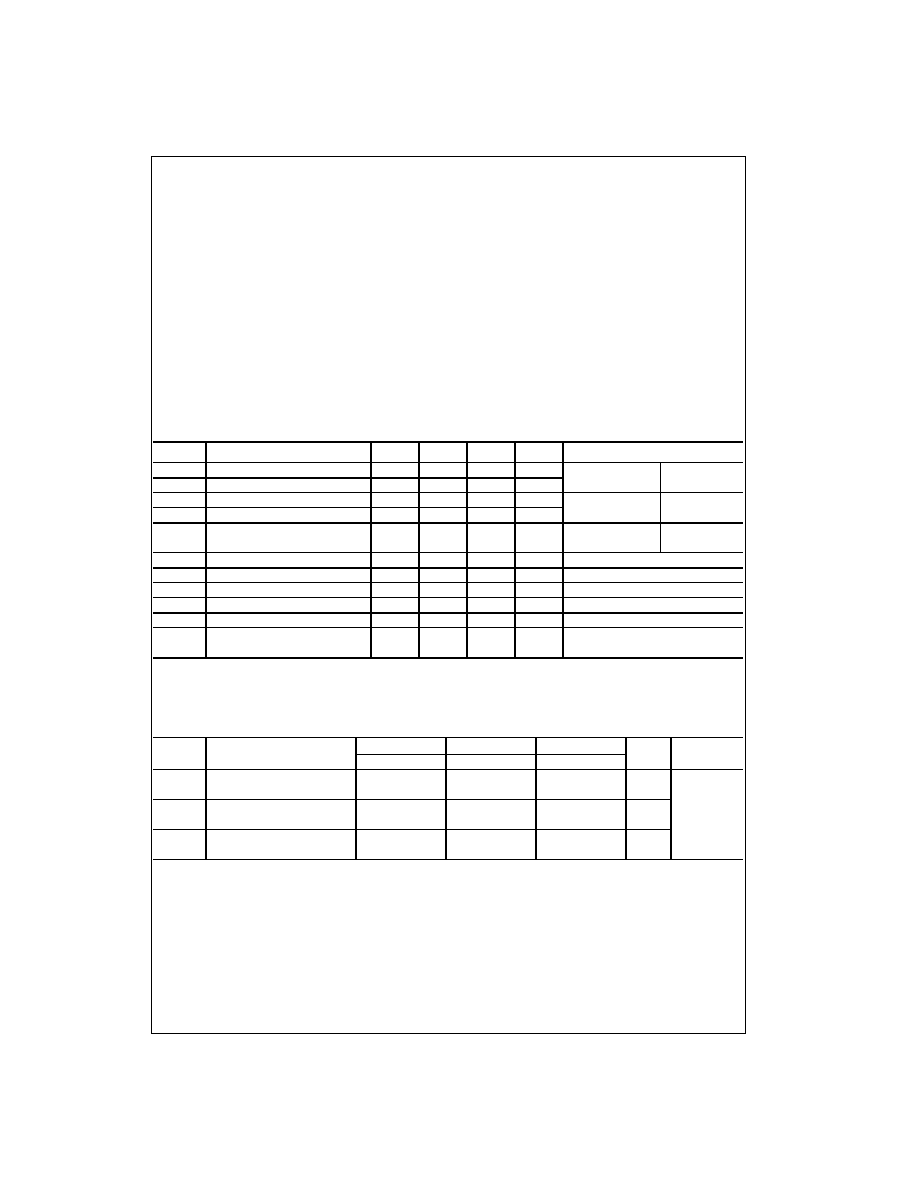
Absolute Maximum Ratings
(Note 1)
Recommended Operating
Conditions
Note 1: The "Absolute Maximum Ratings" are those values beyond which
the safety of the device cannot be guaranteed. The device should not be
operated at these limits. The parametric values defined in the Electrical
Characteristics tables are not guaranteed at the absolute maximum rating.
The "Recommended Operating Conditions" table will define the conditions
for actual device operation.
Note 2: ESD testing conforms to MIL-STD-883, Method 3015.
Commercial Version
DC Electrical Characteristics
(Note 3)
V
EE
=
-
4.2V to
-
5.7V, V
CC
=
V
CCA
=
GND, T
C
=
0
∞
C to
+
85
∞
C
Note 3: The specified limits represent the "worst case" value for the parameter. Since these values normally occur at the temperature extremes, additional
noise immunity and guardbanding can be achieved by decreasing the allowable system operating ranges. Conditions for testing shown in the tables are cho-
sen to guarantee operation under "worst case" conditions.
AC Electrical Characteristics
V
EE
=
-
4.2V to
-
5.7V, V
CC
=
V
CCA
=
GND
Storage Temperature (T
STG
)
-
65
∞
C to
+
150
∞
C
Maximum Junction Temperature (T
J
)
+
150
∞
C
Pin Potential to Ground Pin (V
EE
)
-
7.0V to
+
0.5V
Input Voltage (DC)
V
EE
to
+
0.5V
Output Current (DC Output HIGH)
-
100 mA
ESD (Note 2)
2000V
Case Temperature (T
C
)
Commercial
0
∞
C to
+
85
∞
C
Industrial
-
40
∞
C to
+
85
∞
C
Supply Voltage (V
EE
)
-
5.7V to
-
4.2V
Symbol
Parameter
Min
Typ
Max
Units
Conditions
V
OH
Output HIGH Voltage
-
1025
-
955
-
870
mV
V
IN
=
V
IH(Max)
Loading with
V
OL
Output LOW Voltage
-
1830
-
1705
-
1620
mV
or V
IL(Min)
25
to
-
2.0V
V
OHC
Output HIGH Voltage
-
1035
mV
V
IN
=
V
IH(Min)
Loading
with
V
OLC
Output LOW Voltage
-
1610
mV
or V
IL(Max)
25
to
-
2.0V
V
OLZ
Cut-Off LOW
-
1950
mV
V
IN
=
V
IH(Min)
OE
=
LOW
Voltage
or V
IL(Max)
V
IH
Input HIGH Voltage
-
1110
-
870
mV
Guaranteed HIGH Signal for All Inputs
V
IL
Input LOW Voltage
-
1830
-
1530
mV
Guaranteed LOW Signal for All Inputs
I
IL
Input LOW Current
100
µ
A
V
IN
=
V
IL(Min)
I
IH
Input HIGH Current
360
µ
A
V
IN
=
V
IH(Max)
I
EE
Power Supply Current, Normal
-
119
-
30
mA
I
EEZ
Power Supply
-
219
-
75
mA
Inputs Open,
Current, Cut-Off
OE
=
LOW
Symbol
Parameter
T
C
=
0
∞
C
T
C
=
+
25
∞
C
T
C
=
+
85
∞
C
Units
Conditions
Min
Max
Min
Max
Min
Max
t
PLH
Propagation Delay
0.65
2.10
0.65
2.10
0.65
2.10
ns
Figures 1, 2
t
PHL
Data to Output
t
PZH
Propagation Delay
1.8
4.1
1.8
4.1
1.8
4.1
ns
t
PHZ
OE to Output
1.2
2.9
1.2
2.9
1.2
2.9
t
TLH
Transition Time
0.45
1.30
0.45
1.30
0.45
1.30
ns
t
THL
20% to 80%, 80% to 20%
www.fairchildsemi.com
4
100319
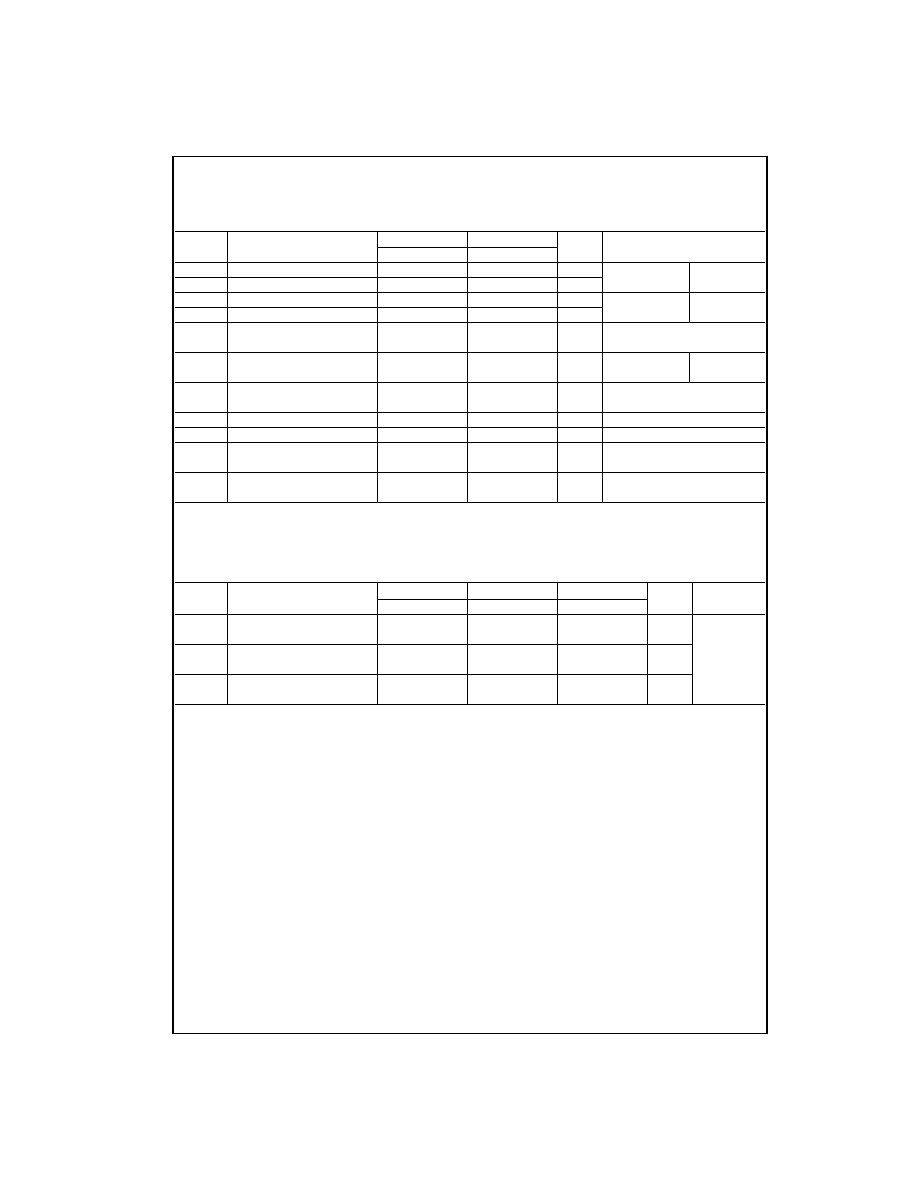
Industrial Version
DC Electrical Characteristics
(Note 4)
V
EE
=
-
4.2V to
-
5.7V, V
CC
=
V
CCA
=
GND
Note 4: The specified limits represent the "worst case" value for the parameter. Since these values normally occur at the temperature extremes, additional
noise immunity and guardbanding can be achieved by decreasing the allowable system operating ranges. Conditions for testing shown in the tables are cho-
sen to guarantee operation under "worst case" conditions.
AC Electrical Characteristics
V
EE
=
-
4.2V to
-
5.7V, V
CC
=
V
CCA
=
GND
Symbol
Parameter
T
C
=
-
40
∞
C
T
C
=
0
∞
C to
+
85
∞
C
Units
Conditions
Min
Max
Min
Max
V
OH
Output HIGH Voltage
-
1085
-
870
-
1025
-
870
mV
V
IN
=
V
IH(Max)
Loading with
V
OL
Output LOW Voltage
-
1830
-
1575
-
1830
-
1620
mV or
V
IL(Min)
25
to
-
2.0V
V
OHC
Output HIGH Voltage
-
1095
-
1035
mV
V
IN
=
V
IH(Min)
Loading with
V
OLC
Output LOW Voltage
-
1565
-
1610
mV or
V
IL(Max)
25
to
-
2.0V
V
IH
Input HIGH Voltage
-
1115
-
870
-
1110
-
870
mV
Guaranteed HIGH Signal for All
Inputs
V
OLZ
Cut-Off LOW Voltage
-
1900
-
1950
mV
V
IN
=
V
IH(Min)
OE
=
LOW
or V
IL(Max)
V
IL
Input LOW Voltage
-
1830
-
1535
-
1830
-
1530
mV
Guaranteed LOW Signal for
All Inputs
I
IL
Input LOW Current
130
100
µ
A
V
IN
=
V
IL(Min)
I
IH
Input HIGH Current
360
360
µ
A
V
IN
=
V
IH(Max)
I
EE
Power Supply Current,
-
119
-
30
-
119
-
30
mA
Normal
I
EEZ
Power Supply Current,
-
219
-
75
-
219
-
75
mA
Inputs Open
Cut-Off
OE
=
LOW
Symbol
Parameter
T
C
=
-
40
∞
C
T
C
=
+
25
∞
C
T
C
=
+
85
∞
C
Units
Conditions
Min
Max
Min
Max
Min
Max
t
PLH
Propagation Delay
0.65
2.10
0.65
2.10
0.65
2.10
ns
Figures 1Figure
2
t
PHL
Data to Output
t
PZH
Propagation Delay
1.8
4.1
1.8
4.1
1.8
4.1
ns
t
PHZ
OE to Output
1.2
2.9
1.2
2.9
1.2
2.9
t
TLH
Transition Time
0.45
1.30
0.45
1.30
0.45
1.30
ns
t
THL
20% to 80%, 80% to 20%
5
www.fairchildsemi.com
1
00319
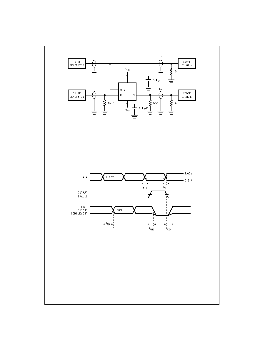
Test Circuitry
Notes:
V
CC
, V
CCA
=
+
2V, V
EE
=
-
2.5V
L1 and L2
=
equal length 50
impedance lines
R
T
=
50
terminator internal to scope
Decoupling 0.1
µ
F from GND to V
CC
and V
EE
All unused outputs are loaded with 25
to GND
C
L
=
Fixture and stray capacitance
3 pF
FIGURE 1. AC Test Circuit
Switching Waveforms
Note: The output AC measurement point for cut-off propagation delay testing
=
the 50% voltage point between active V
OL
and V
OH
.
FIGURE 2. Propagation Delay, Cut-Off and Transition Times