 | –≠–ª–µ–∫—Ç—Ä–æ–Ω–Ω—ã–π –∫–æ–º–ø–æ–Ω–µ–Ω—Ç: 100328PC | –°–∫–∞—á–∞—Ç—å:  PDF PDF  ZIP ZIP |
© 2000 Fairchild Semiconductor Corporation
DS010219
www.fairchildsemi.com
April 1989
Revised August 2000
1
00328 Low
Power Octal
ECL/
TTL
Bi
-Di
r
ect
i
onal T
r
ans
l
at
or w
i
t
h
Lat
c
h
100328
Low Power Octal ECL/TTL Bi-Directional Translator
with Latch
General Description
The 100328 is an octal latched bi-directional translator
designed to convert TTL logic levels to 100K ECL logic lev-
els and vice versa. The direction of this translation is deter-
mined by the DIR input. A LOW on the output enable input
(OE) holds the ECL outputs in a cut-off state and the TTL
outputs at a high impedance level. A HIGH on the latch
enable input (LE) latches the data at both inputs even
though only one output is enabled at the time. A LOW on
LE makes the 100328 transparent.
The cut-off state is designed to be more negative than a
normal ECL LOW level. This allows the output emitter-fol-
lowers to turn off when the termination supply is
-
2.0V, pre-
senting a high impedance to the data bus. This high
impedance reduces termination power and prevents loss of
low state noise margin when several loads share the bus.
The 100328 is designed with FAST
TTL output buffers,
featuring optimal DC drive and capable of quickly charging
and discharging highly capacitive loads. All inputs have
50 k
pull-down resistors.
Features
s
Identical performance to the 100128 at 50% of the
supply current
s
Bi-directional translation
s
2000V ESD protection
s
Latched outputs
s
FAST TTL outputs
s
3-STATE outputs
s
Voltage compensated operating range
=
-
4.2V to
-
5.7V
s
Available to industrial grade temperature range
Ordering Code:
Devices also available in Tape and Reel. Specify by appending the suffix letter "X" to the ordering code.
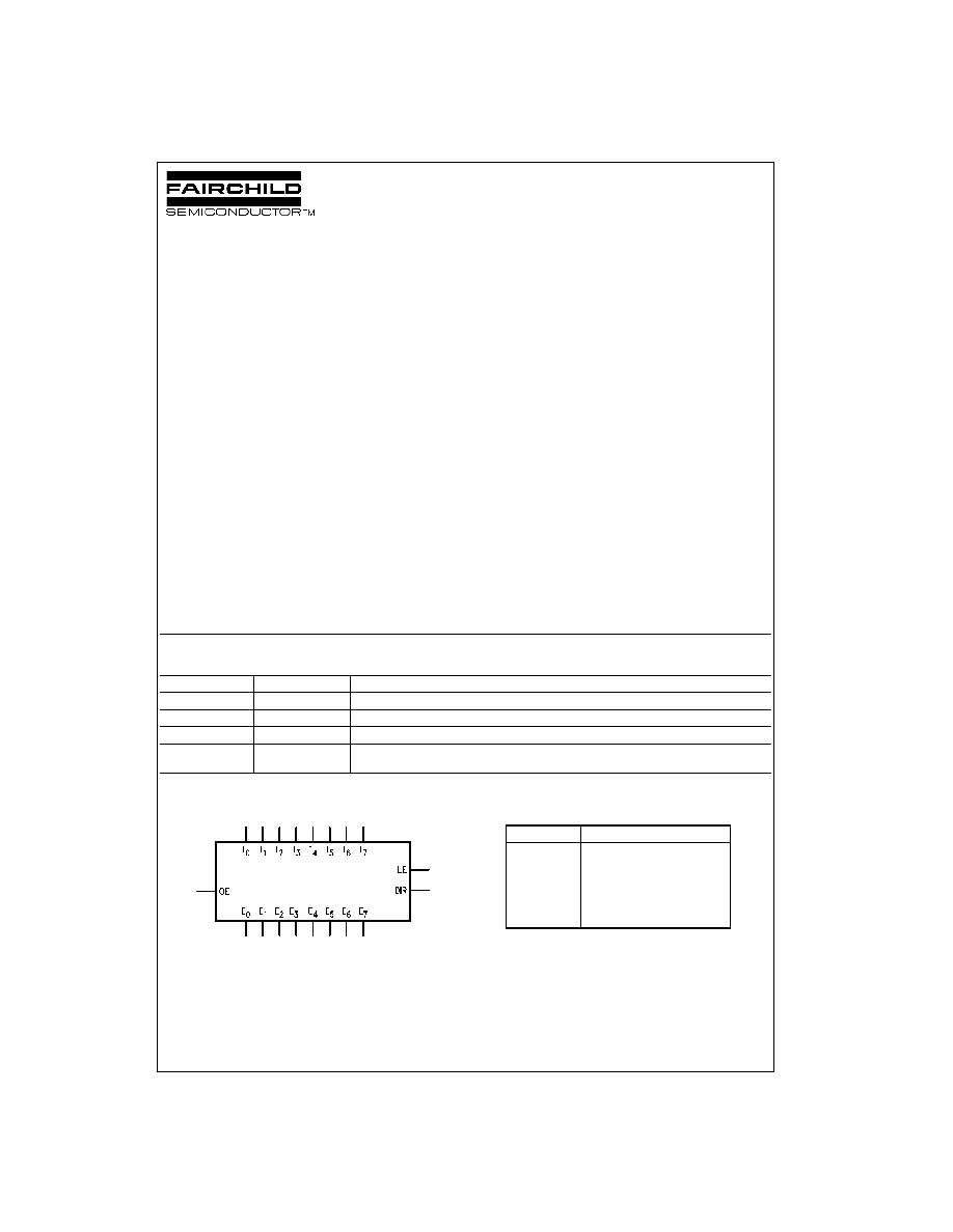
Logic Symbol
Pin Descriptions
All pins function at 100K ECL levels except for T
0
≠T
7
.
FAST
is a registered trademark of Fairchild Semiconductor Corporation.
Order Number
Package Number
Package Description
100328SC
M24B
24-Lead Small Outline Integrated Circuit (SOIC), JEDEC MS-013, 0.300 Wide
100328PC
N24E
24-Lead Plastic Dual-In-Line Package (PDIP), JEDEC MS-010, 0.400 Wide
100328QC
V28A
28-Lead Plastic Lead Chip Carrier (PLCC), JEDEC MO-047, 0.450 Square
100328QI
V28A
28-Lead Plastic Lead Chip Carrier (PLCC), JEDEC MO-047, 0.450 Square
Industrial Temperature Range (
-
40
∞
C to
+
85
∞
C)
Pin Names
Description
E
0
≠E
7
ECL Data I/O
T
0
≠T
7
TTL Data I/O
OE
Output Enable Input
LE
Latch Enable Input
DIR
Direction Control Input

www.fairchildsemi.com
2
100328
Connection Diagrams
24-Pin DIP/SOIC
28-Pin PLCC
Truth Table
H
=
HIGH Voltage Level
L
=
LOW Voltage Level
X
=
Don't Care
Z
=
High Impedance
Note 1: ECL input to TTL output mode.
Note 2: TTL input to ECL output mode.
Note 3: Retains data present before LE set HIGH.
Note 4: Latch is transparent.
Functional Diagram
Note: LE, DIR, and OE use ECL logic levels
Detail
OE
DIR
LE
ECL
TTL
Notes
Port
Port
L
X
L
LOW
Z
(Cut-Off)
L
L
H
Input
Z
(Note 1)(Note 3)
L
H
H
LOW
Input
(Note 2)(Note 3)
(Cut-Off)
H
L
L
L
L
(Note 1)(Note 4)
H
L
L
H
H
(Note 1)(Note 4)
H
L
H
X
Latched (Note 1)(Note 3)
H
H
L
L
L
(Note 2)(Note 4)
H
H
L
H
H
(Note 2)(Note 4)
H
H
H
Latched
X
(Note 2)(Note 4)

3
www.fairchildsemi.com
1
00328
Absolute Maximum Ratings
(Note 5)
Recommended Operating
Conditions
Note 5: The "Absolute Maximum Ratings" are those values beyond which
the safety of the device cannot be guaranteed. The device should not be
operated at these limits. The parametric values defined in the Electrical
Characteristics tables are not guaranteed at the absolute maximum rating.
The "Recommended Operating Conditions" table will define the conditions
for actual device operation.
Note 6: Either voltage limit or current limit is sufficient to protect inputs.
Note 7: ESD testing conforms to MIL-STD-883, Method 3015.
Commercial Version
TTL-to-ECL DC Electrical Characteristics
(Note 8)
V
EE
=
-
4.2V to
-
5.7V, V
CC
=
V
CCA
=
GND, T
C
=
0
∞
C to
+
85
∞
C, V
TTL
=
+
4.5V to
+
5.5V
Note 8: The specified limits represent the "worst case" value for the parameter. Since these values normally occur at the temperature extremes, additional
noise immunity and guardbanding can be achieved by decreasing the allowable system operating ranges. Conditions for testing shown in the tables are cho-
sen to guarantee operation under "worst case" conditions.
Storage Temperature (T
STG
)
-
65
∞
C to
+
150
∞
C
Maximum Junction Temperature (T
J
)
+
150
∞
C
V
EE
Pin Potential to Ground Pin
-
7.0V to
+
0.5V
V
TTL
Pin Potential to Ground Pin
-
0.5V to
+
6.0V
ECL Input Voltage (DC)
V
EE
to
+
0.5V
ECL Output Current
(DC Output HIGH)
-
50 mA
TTL Input Voltage (Note 6)
-
0.5V to
+
6.0V
TTL Input Current (Note 6)
-
30 mA to
+
5.0 mA
Voltage Applied to Output
in HIGH State
3-STATE Output
-
0.5V to
+
5.5V
Current Applied to TTL
Output in LOW State (Max)
twice the rated I
OL
(mA)
ESD (Note 7)
2000V
Case Temperature (T
C
)
Commercial
0
∞
C to
+
85
∞
C
Industrial
-
40
∞
C to
+
85
∞
C
ECL Supply Voltage (V
EE
)
-
5.7V to
-
4.2V
TTL Supply Voltage (V
TTL
)
+
4.5V to
+
5.5V
Symbol
Parameter
Min
Typ
Max
Units
Conditions
V
OH
Output HIGH Voltage
-
1025
-
955
-
870
mV
V
IN
=
V
IH(Max)
or V
IL(Min)
V
OL
Output LOW Voltage
-
1830
-
1705
-
1620
mV
Loading with 50
to
-
2V
Cutoff Voltage
OE or DIR LOW,
-
2000
-
1950
mV
V
IN
=
V
IH(Max)
or V
IL(Min)
,
Loading with 50
to
-
2V
V
OHC
Output HIGH Voltage
-
1035
mV
Corner Point HIGH
V
IN
=
V
IH(Min)
or V
IL(Max)
V
OLC
Output LOW Voltage
-
1610
mV
Loading with 50
to
-
2V
Corner Point LOW
V
IH
Input HIGH Voltage
2.0
5.0
V
Over V
TTL
, V
EE
, T
C
Range
V
IL
Input LOW Voltage
0
0.8
V
Over V
TTL
, V
EE
, T
C
Range
I
IH
Input HIGH Current
70
µ
A
V
IN
=
+
2.7V
Breakdown Test
1.0
mA
V
IN
=
+
5.5V
I
IL
Input LOW Current
-
700
µ
A
V
IN
=
+
0.5V
V
FCD
Input Clamp Diode Voltage
-
1.2
V
I
IN
=
-
18 mA
I
EE
V
EE
Supply Current
LE LOW, OE and DIR HIGH
Inputs OPEN
-
159
-
75
mA
V
EE
=
-
4.2V to
-
4.8V
-
169
-
75
V
EE
=
-
4.2V to
-
5.7V
www.fairchildsemi.com
4
100328
Commercial Version
(Continued)
ECL-to-TTL DC Electrical Characteristics
(Note 9)
V
EE
=
-
4.2V to
-
5.7V, V
CC
=
V
CCA
=
GND, T
C
=
0
∞
C to
+
85
∞
C, C
L
=
50 pF, V
TTL
=
+
4.5V to
+
5.5V
DIP TTL-to-ECL AC Electrical Characteristics
(Note 9)
V
EE
=
-
4.2V to
-
5.7V, V
TTL
=
+
4.5V to
+
5.5V, V
CC
=
V
CCA
=
GND
Note 9: The specified limits represent the "worst" case value for the parameter. Since these values normally occur at the temperature extremes, additional
noise immunity and guardbanding can be achieved by decreasing the allowable system operating ranges. Conditions for testing shown in the tables are cho-
sen to guarantee operation under "worst case" conditions.
Symbol
Parameter
Min
Typ
Max
Units
Conditions
V
OH
Output HIGH Voltage
2.7
3.1
V
I
OH
=
-
3 mA, V
TTL
=
4.75V
2.4
2.9
I
OH
=
-
3 mA, V
TTL
=
4.50V
V
OL
Output LOW Voltage
0.3
0.5
V
I
OL
=
24 mA, V
TTL
=
4.50V
V
IH
Input HIGH Voltage
-
1165
-
870
mV
Guaranteed HIGH Signal for All Inputs
V
IL
Input LOW Voltage
-
1830
-
1475
mV
Guaranteed LOW Signal for All Inputs
I
IH
Input HIGH Current
350
µ
A
V
IN
=
V
IH
(Max)
I
IL
Input LOW Current
0.50
µ
A
V
IN
=
V
IL
(Min)
I
OZHT
3-STATE Current Output HIGH
70
µ
A
V
OUT
=
+
2.7V
I
OZLT
3-STATE Current Output LOW
-
700
µ
A
V
OUT
=
+
0.5V
I
OS
Output Short-Circuit Current
-
150
-
60
mA
V
OUT
=
0.0V, V
TTL
=
+
5.5V
I
TTL
V
TTL
Supply Current
74
mA
TTL Outputs LOW
49
mA
TTL Outputs HIGH
67
mA
TTL Outputs in 3-STATE
Symbol
Parameter
T
C
=
0
∞
C
T
C
=
25
∞
C
T
C
=
85
∞
C
Units
Conditions
Min
Max
Min
Max
Min
Max
t
PLH
T
N
to E
n
1.1
3.5
1.1
3.6
1.1
3.8
ns
Figures 1, 2
t
PHL
(Transparent)
t
PLH
LE to E
n
1.7
3.6
1.7
3.7
1.9
3.9
ns
Figures 1, 2
t
PHL
t
PZH
OE to E
n
1.3
4.2
1.5
4.4
1.7
4.8
ns
Figures 1, 2
(Cutoff to HIGH)
t
PHZ
OE to E
n
1.5
4.5
1.6
4.5
1.6
4.6
ns
Figures 1, 2
(HIGH to Cutoff)
t
PHZ
DIR to E
n
1.6
4.3
1.6
4.3
1.7
4.5
ns
Figures 1, 2
(HIGH to Cutoff)
t
SET
T
n
to LE
1.1
1.1
1.1
ns
Figures 1, 2
t
HOLD
T
n
to LE
1.1
1.1
1.1
ns
Figures 1, 2
t
PW
(H)
Pulse Width LE
2.1
2.1
2.1
ns
Figures 1, 2
t
TLH
Transition Time
0.6
1.6
0.6
1.6
0.6
1.6
ns
Figures 1, 2
t
THL
20% to 80%, 80% to 20%
5
www.fairchildsemi.com
1
00328
Commercial Version
(Continued)
DIP ECL-to-TTL AC Electrical Characteristics
V
EE
=
-
4.2V to
-
5.7V, V
TTL
=
+
4.5V to
+
5.5V, V
CC
=
V
CCA
=
GND, C
L
=
50 pF
SOIC and PLCC TTL-to-ECL AC Electrical Characteristics
V
EE
=
-
4.2V to
-
5.7V, V
TTL
=
+
4.5V to
+
5.5V
Note 10: Output-to-Output Skew is defined as the absolute value of the difference between the actual propagation delay for any outputs within the same
packaged device. The specifications apply to any outputs switching in the same direction either HIGH-to-LOW (t
OSHL
), or LOW-to-HIGH (t
OSLH
), or in oppo-
site directions both HL and LH (t
OST
). Parameters t
OST
and t
ps
guaranteed by design.
Symbol
Parameter
T
C
=
0
∞
C
T
C
=
25
∞
C
T
C
=
85
∞
C
Units
Conditions
Min
Max
Min
Max
Min
Max
t
PLH
E
n
to T
n
2.3
5.6
2.4
5.6
2.6
5.9
ns
Figures 3, 4
t
PHL
(Transparent)
t
PLH
LE to T
n
3.1
7.2
3.1
7.2
3.3
7.7
ns
Figures 3, 4
t
PHL
t
PZH
OE to T
n
3.4
8.45
3.7
8.95
4.0
9.7
ns
Figures 3, 5
t
PZL
(Enable Time)
3.8
9.2
4.0
9.2
4.3
9.95
t
PHZ
OE to T
n
3.2
8.95
3.3
8.95
3.5
9.2
ns
Figures 3, 5
t
PLZ
(Disable Time)
3.0
7.7
3.4
8.7
4.1
9.95
t
PHZ
DIR to T
n
2.7
8.2
2.8
8.7
3.1
8.95
ns
Figures 3, 6
t
PLZ
(Disable Time)
2.8
7.45
3.1
7.95
4.0
9.2
t
SET
E
n
to LE
1.1
1.1
1.1
ns
Figures 3, 6
t
HOLD
E
n
to LE
2.1
2.1
2.6
ns
Figures 3, 4
t
PW
(H)
Pulse Width LE
4.1
4.1
4.1
ns
Figures 3, 7
Symbol
Parameter
T
C
=
0
∞
C
T
C
=
25
∞
C
T
C
=
85
∞
C
Units
Conditions
Min
Max
Min
Max
Min
Max
t
PLH
T
n
to E
n
1.1
3.3
1.1
3.4
1.1
3.6
ns
Figures 1, 2
t
PHL
(Transparent)
t
PLH
LE to E
n
1.7
3.4
1.7
3.5
1.9
3.7
ns
Figures 1, 2
t
PHL
t
PZH
OE to E
n
1.3
4.0
1.5
4.2
1.7
4.6
ns
Figures 1, 2
(Cutoff to HIGH)
t
PHZ
OE to E
n
1.5
4.3
1.6
4.3
1.6
4.4
ns
Figures 1, 2
(HIGH to Cutoff)
t
PHZ
DIR to E
n
1.6
4.1
1.6
4.1
1.7
4.3
ns
Figures 1, 2
(HIGH to Cutoff)
t
SET
T
n
to LE
1.0
1.0
1.0
ns
Figures 1, 2
t
HOLD
T
n
to LE
1.0
1.0
1.0
ns
Figures 1, 2
t
PW
(H)
Pulse Width LE
2.0
2.0
2.0
ns
Figures 1, 2
t
TLH
Transition Time
0.6
1.6
0.6
1.6
0.6
1.6
ns
Figures 1, 2
t
THL
20% to 80%, 80% to 20%
t
OSHL
Maximum Skew Common Edge
PLCC Only
Output-to-Output Variation
200
200
200
ps
(Note 10)
Data to Output Path
t
OSLH
Maximum Skew Common Edge
PLCC Only
Output-to-Output Variation
200
200
200
ps
(Note 10)
Data to Output Path
t
OST
Maximum Skew Opposite Edge
PLCC Only
Output-to-Output Variation
650
650
650
ps
(Note 10)
Data to Output Path
t
PS
Maximum Skew
PLCC Only
Pin (Signal) Transition Variation
650
650
650
ps
(Note 10)
Data to Output Path