 | –≠–ª–µ–∫—Ç—Ä–æ–Ω–Ω—ã–π –∫–æ–º–ø–æ–Ω–µ–Ω—Ç: 100EL11M | –°–∫–∞—á–∞—Ç—å:  PDF PDF  ZIP ZIP |

© 2003 Fairchild Semiconductor Corporation
DS500769
www.fairchildsemi.com
January 2003
Revised January 2003
1
00EL1
1 5
V
ECL 1
:
2
Dif
f
er
enti
al
Fanout
Buf
f
e
r
100EL11
5V ECL 1:2 Differential Fanout Buffer
General Description
The 100EL11 is a 5V 1:2 differential fanout buffer. One dif-
ferential input signal is fanned out to two identical differen-
tial outputs. By supplying a constant reference level to one
input pin a single ended input condition is created.
With inputs open or both inputs at V
EE
the differential Q
outputs default LOW and Q outputs default HIGH.
The 100 series is temperature compensated.
Features
s
Typical propagation delay of 265 ps
s
Typical I
EE
of 26 mA
s
Typical Skew of 5 ps between outputs
s
Internal pull-down resistors on inputs
s
Fairchild MSOP-8 package is a drop-in replacement to
ON TSSOP-8
s
Meets or exceeds JEDEC specification EIA/JESD78 IC
latch-up test
s
Moisture Sensitivity Level 1
s
ESD Performance:
Human Body Model
>
2000V
Machine Model
>
200V
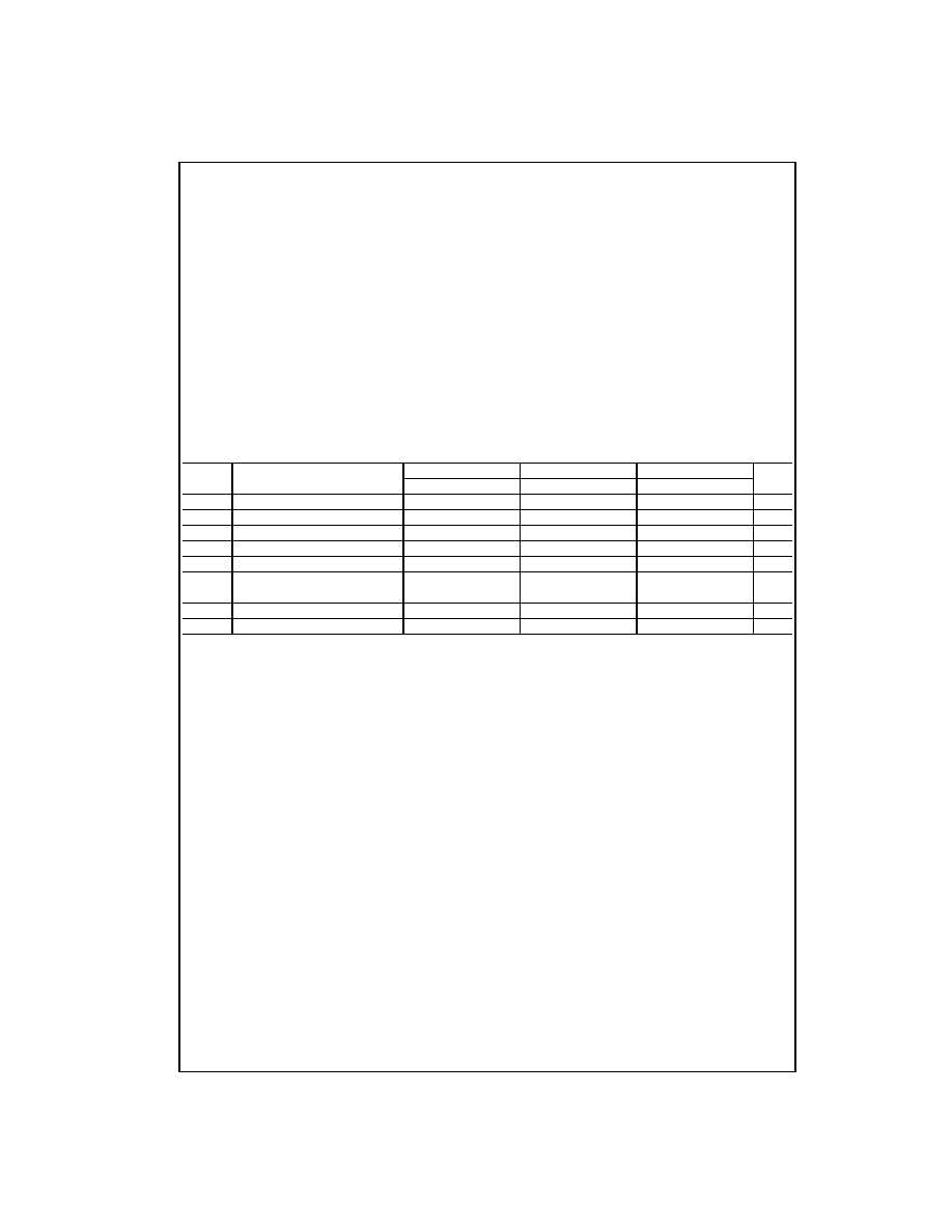
Ordering Code:
Devices also available in Tape and Reel. Specify by appending suffix letter "X" to the ordering code.
Connection Diagram
Top View
Pin Descriptions
Logic Diagram
Order Number
Product
Package Description
Package
Code
Number
Top Mark
100EL11M
M08A
KEL11
8-Lead Small Outline Integrated Circuit (SOIC), JEDEC MS-012, 0.150" Narrow
100EL11M8
(Preliminary)
MA08D
KL11
8-Lead Molded Small Outline Package (MSOP), JEDEC MO-187, 3.0mm Wide
Pin Name
Description
Q
0
, Q
0
, Q
1
, Q
1
ECL Data Outputs
D, D
ECL Data Inputs
V
CC
Positive Supply
V
EE
Negative Supply
www.fairchildsemi.com
2
100EL1
1
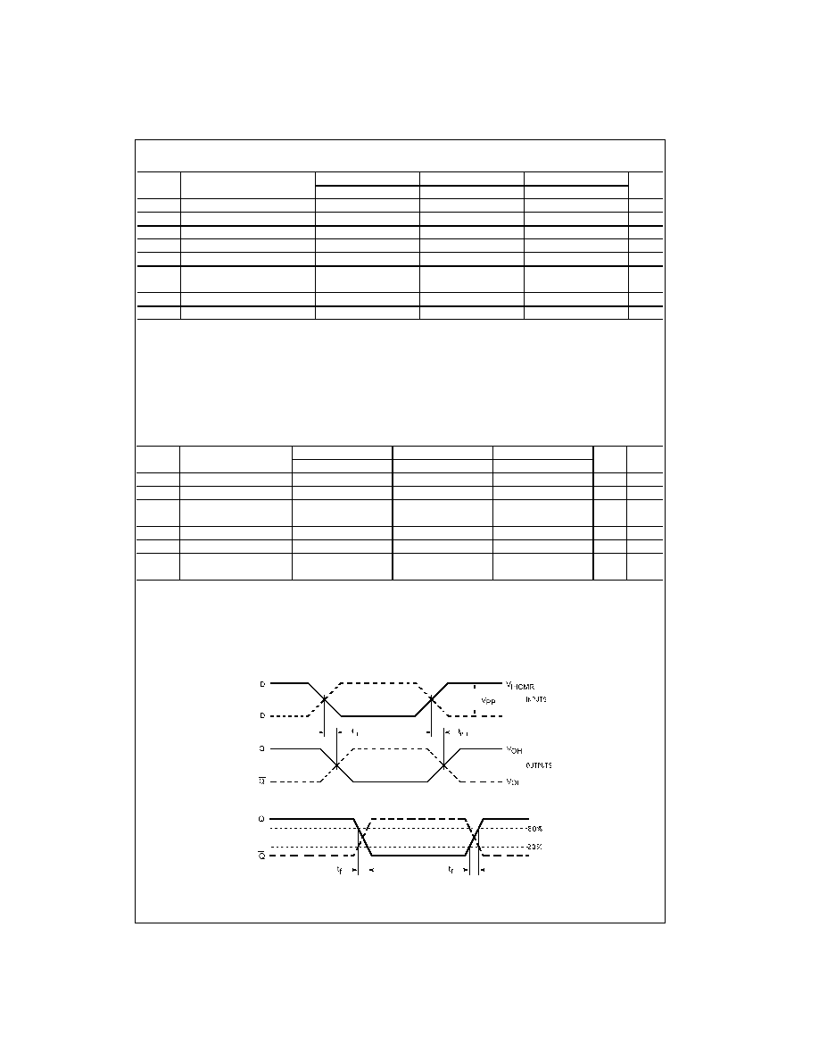
Absolute Maximum Ratings
(Note 1)
Recommended Operating
Conditions
Note 1: The "Absolute Maximum Ratings" are those values beyond which
the safety of the device cannot be guaranteed. The device should not be
operated at these limits. The parametric values defined in the Electrical
Characteristics tables are not guaranteed at the absolute maximum rating.
The "Recommended Operating Conditions" table will define the conditions
for actual device operation.
100EL PECL DC Electrical Characteristics
V
CC
=
5.0V; V
EE
=
0.0V (Note 2)
Note 2: Input and output parameters vary 1 to 1 with V
CC
. V
EE
can vary
+
0.8V/
-
0.5V.
Note 3: Outputs are terminated through a 50
Resistor to V
CC
-
2.0V.
Note 4: V
IHCMR
minimum varies 1 to 1 with V
EE
. V
IHCMR
maximum varies 1 to 1 with V
CC
. The V
IHCMR
range is referenced to the most positive side of the dif-
ferential input signal. Normal operation is obtained if the HIGH level falls within the specified range and the peak-to-peak voltage lies between V
PPMIN
and
1V.
Note 5: Absolute value of the input HIGH and LOW current should not exceed the absolute value of the stated MIn or Max specification.
Note: Devices are designed to meet the DC specifications after thermal equilibrium has been established. Circuit is tested with air flow greater than
500LFPM maintained.
PECL Supply Voltage (V
CC
) V
EE
=
0V
0.0V to
+
8.0V
NECL Supply Voltage (V
EE
) V
CC
=
0V
0.0V to
-
8.0V
PECL DC Input Voltage (V
I
) V
EE
=
0V
0.0V to
+
6.0V
NECL DC Input Voltage (V
I
) V
CC
=
0V
0.0V to
-
6.0V
DC Output Current (I
OUT
)
Continuous
50 mA
Surge
100 mA
Storage Temperature (T
STG
)
-
65
∞
C to
+
150
∞
C
PECL Power Supply
(V
EE
=
0V)
V
CC
=
4.2V to 5.5V
NECL Power Supply
(V
CC
=
0V)
V
EE
=
-
4.2V to
-
5.5V
Free Air Operating Temperature (T
A
)
-
40
∞
C to
+
85
∞
C
Symbol
Parameter
-
40
∞
C
25
∞
C
85
∞
C
Units
Min
Typ
Max
Min
Typ
Max
Min
Typ
Max
I
EE
Power Supply Current
26
31
26
31
30
36
mA
V
OH
Output HIGH Voltage (Note 3)
3915
3995
4120
3975
4045
4120
3975
4050
4120
mV
V
OL
Output LOW Voltage (Note 3)
3170
3305
3445
3190
3295
3380
3190
3295
3380
mV
V
IH
Input HIGH Voltage (Single Ended)
3835
4120
3835
4120
3835
4120
mV
V
IL
Input LOW Voltage (Single Ended)
3190
3525
3190
3525
3190
3525
mV
V
IHCMR
Input HIGH Voltage Common Mode
2.5
4.6
2.5
4.6
2.5
4.6
V
Range (Differential) (Note 4)
I
IH
Input HIGH Current (Note 5)
150
150
150
µ
A
I
IL
Input LOW Current (Note 5)
0.5
0.5
0.5
µ
A
3
www.fairchildsemi.com
1
00EL1
1
100EL NECL DC Electrical Characteristics
V
CC
=
0.0V; V
EE
=
-
5.0V (Note 6)
Note 6: Input and output parameters vary 1 to 1 with V
CC
. V
EE
can vary
+
0.8V/
-
0.5V.
Note 7: Outputs are terminated through a 50
Resistor to V
CC
-
2.0V.
Note 8: V
IHCMR
minimum varies 1 to 1 with V
EE
. V
IHCMR
maximum varies 1 to 1 with V
CC
. The V
IHCMR
range is referenced to the most positive side of the dif-
ferential input signal. Normal operation is obtained if the HIGH level falls within the specified range and the peak-to-peak voltage lies between V
PPMIN
and
1V.
Note 9: Absolute value of the input HIGH and LOW current should not exceed the absolute value of the stated Min or Max specification.
Note: Devices are designed to meet the DC specifications after thermal equilibrium has been established. Circuit is tested with air flow greater than
500LFPM maintained.
AC Electrical Characteristics
V
CC
=
5V; V
EE
=
0.0V or V
CC
=
0.0V; V
EE
=
-
5V (Note 10)(Note 11)
Note 10: V
EE
can vary
+
0.8V /
-
0.5V.
Note 11: Measured using a 750 mV input swing centered at V
CC
- 1.32V; 50% duty cycle clock source; t
r
=
t
f
=
250 ps (20% - 80%) at f
IN
=
1 MHz. All loading
with 50
to V
CC
-
2.0V.
Note 12: Within-device skew defined as identical transitions on similar paths through a device.
Note 13: Duty cycle skew is the difference between a t
PLH
and t
PHL
propagation delay through a device under identical conditions.
Switching Waveforms
FIGURE 1. Differential to Differential Propagation Delay
FIGURE 2. Differential Output Edge Rates
Symbol
Parameter
-
40
∞
C
25
∞
C
85
∞
C
Units
Min
Typ
Max
Min
Typ
Max
Min
Typ
Max
I
EE
Power Supply Current
26
31
26
31
30
36
mA
V
OH
Output HIGH Voltage (Note 7)
-
1085
-
1005
-
880
-
1025
-
955
-
880
-
1025
-
955
-
880
mV
V
OL
Output LOW Voltage (Note 7)
-
1830
-
1695
-
1555
-
1810
-
1705
-
1620
-
1810
-
1705
-
1620
mV
V
IH
Input HIGH Voltage (Single Ended)
-
1165
-
880
-
1165
-
880
-
1165
-
880
mV
V
IL
Input LOW Voltage (Single Ended)
-
1810
-
1475
-
1810
-
1475
-
1810
-1475
mV
V
IHCMR
Input HIGH Voltage Common Mode
-
2.5
-
0.4
-
2.5
-
0.4
-
2.5
-
0.4
V
Range (Differential) (Note 8)
I
IH
Input HIGH Current (Note 9)
150
150
150
µ
A
I
IL
Input LOW Current (Note 9)
0.5
0.5
0.5
µ
A
Symbol
Parameter
-
40
∞
C
25
∞
C
85
∞
C
Units
Figure
Min
Typ
Max
Min
Typ
Max
Min
Typ
Max
Number
f
MAX
Maximum Toggle Frequency
TBD
TBD
TBD
GHz
t
PLH
, t
PHL
Propagation Delay to Output
135
260
385
190
265
340
215
290
365
ps
Figure 1
t
SKEW
Within Device Skew (Note 12)
5
5
20
5
20
ps
Duty Cycle Skew (Note 13)
5
5
20
5
20
t
JITTER
Cycle-to-Cycle Jitter
TBD
TBD
TBD
ps
V
PP
Input Swing
150
1000
150
100
150
1000
mV
Figure 1
t
r
, t
f
Output Rise Times Q
100
225
350
100
225
350
100
225
350
ps
Figure 2
(20% to 80%)

www.fairchildsemi.com
4
100EL1
1
Physical Dimensions
inches (millimeters) unless otherwise noted
8-Lead Small Outline Integrated Circuit (SOIC), JEDEC MS-012, 0.150" Narrow
Package Number M08A
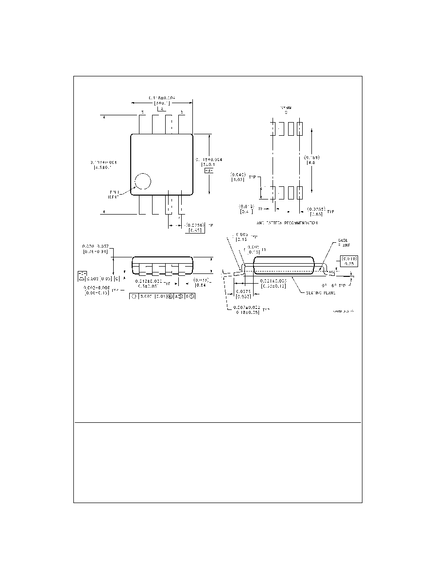
Physical Dimensions
inches (millimeters) unless otherwise noted (Continued)
5
www.fairchildsemi.com
1
00EL1
1 5
V
ECL 1
:
2
Dif
f
er
enti
al
Fanout
Buf
f
e
r
Physical Dimensions
inches (millimeters) unless otherwise noted (Continued)
8-Lead Molded Small Outline Package (MSOP), JEDEC MO-187, 3.0mm Wide
Package Number MA08D
Fairchild does not assume any responsibility for use of any circuitry described, no circuit patent licenses are implied and
Fairchild reserves the right at any time without notice to change said circuitry and specifications.
LIFE SUPPORT POLICY
FAIRCHILD'S PRODUCTS ARE NOT AUTHORIZED FOR USE AS CRITICAL COMPONENTS IN LIFE SUPPORT
DEVICES OR SYSTEMS WITHOUT THE EXPRESS WRITTEN APPROVAL OF THE PRESIDENT OF FAIRCHILD
SEMICONDUCTOR CORPORATION. As used herein:
1. Life support devices or systems are devices or systems
which, (a) are intended for surgical implant into the
body, or (b) support or sustain life, and (c) whose failure
to perform when properly used in accordance with
instructions for use provided in the labeling, can be rea-
sonably expected to result in a significant injury to the
user.
2. A critical component in any component of a life support
device or system whose failure to perform can be rea-
sonably expected to cause the failure of the life support
device or system, or to affect its safety or effectiveness.
www.fairchildsemi.com