© 1999 Fairchild Semiconductor Corporation
DS009606
www.fairchildsemi.com
April 1988
Revised August 1999
2
9F52
∑29F53 8-Bi
t Regi
ster
ed
T
r
anscei
ver
29F52∑29F53
8-Bit Registered Transceiver
General Description
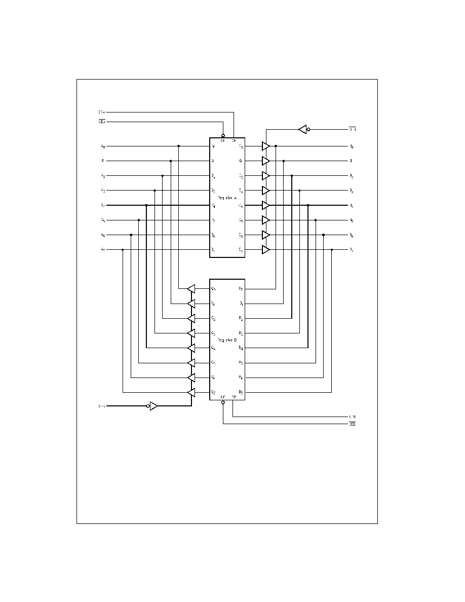
The 29F52 and 29F53 are 8-bit registered transceivers.
Two 8-bit back to back registers store data flowing in both
directions between two bidirectional buses. Separate clock,
clock enable and 3-STATE output enable signals are pro-
vided for each register. The A
0
≠A
7
output pins are guaran-
teed to sink 24 mA while the B
0
≠B
7
output pins are
designed for 64 mA.
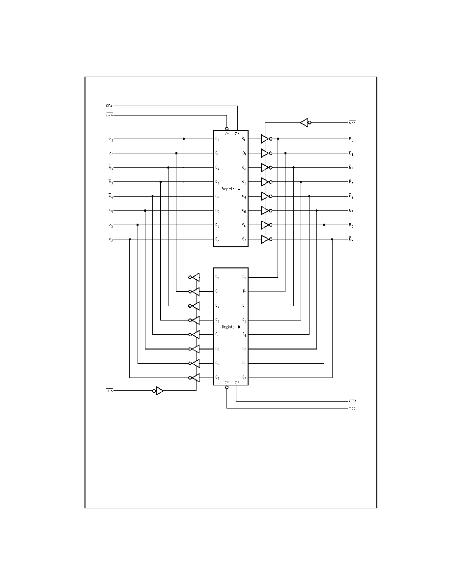
The 29F53 is an inverting option of the 29F52. Both trans-
ceivers are AMD Am2952/2953 functional equivalents.
Features
s
8-bit registered transceivers
s
Separate clock, clock enable and 3-STATE output
enable provided for each register
s
AMD Am2952/2953 functional equivalents
s
Both inverting and non-inverting options available
s
24-Pin slimline package
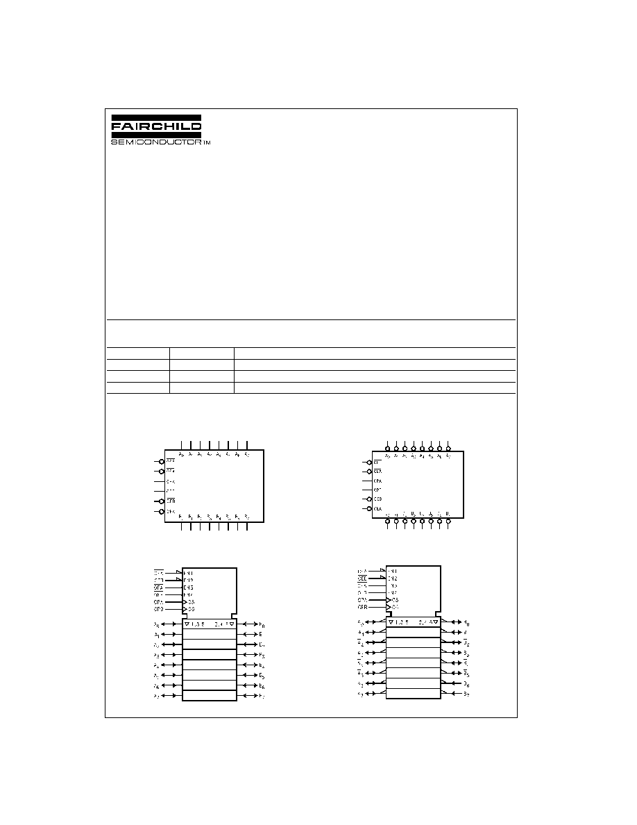
Ordering Code:
Devices also available in Tape and Reel. Specify by appending the suffix letter "X" to the ordering code.
Logic Symbols
29F52
IEEE/IEC
29F52
29F53
IEEE/IEC
29F53
Order Number
Package Number
Package Description
29F52SC
M24B
24-Lead Small Outline Integrated Circuit (SOIC), JEDEC MS-013, 0.300 Wide
29F52SPC
N24C
24-Lead Plastic Dual-In-Line Package (PDIP), JEDEC MS-100, 0.300 Wide
29F53SPC
N24C
24-Lead Plastic Dual-In-Line Package (PDIP), JEDEC MS-100, 0.300 Wide
www.fairchildsemi.com
2
29F52
∑29F53
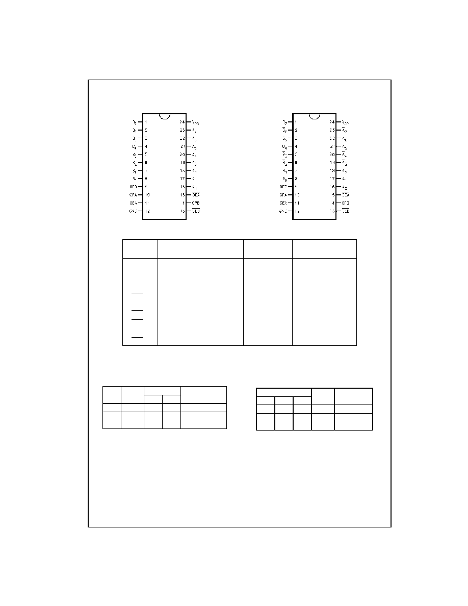
Connection Diagrams
Pin Assignment for DIP and SOIC
29F52
Pin Assignment for DIP
29F53
Unit Loading/Fan Out
Output Control
H
=
HIGH Voltage Level
L
=
LOW Voltage Level
X
=
Immaterial
Z
=
HIGH Impedance
N
=
LOW-to-HIGH Transition
NC
=
No Change
Register Function Table
(Applies to A or B Register)
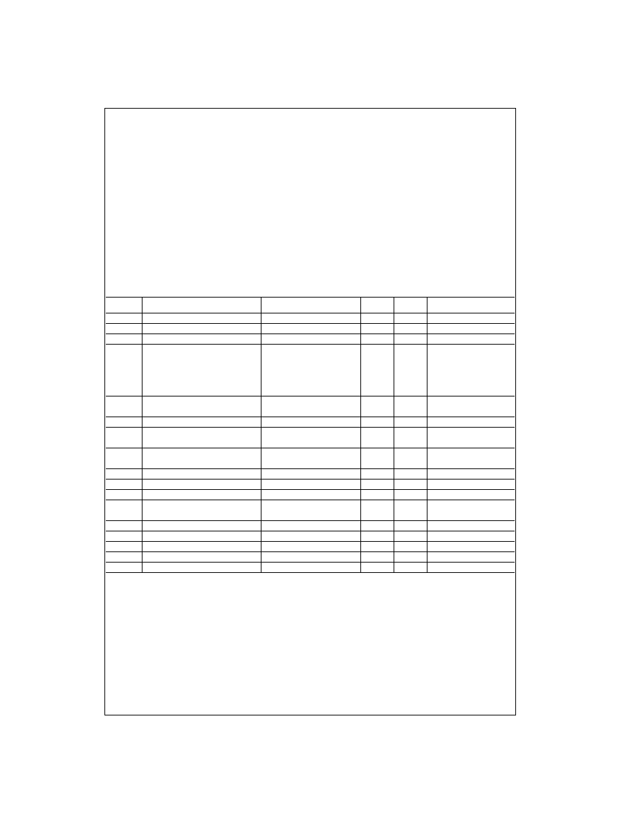
Pin Names
Description
U.L.
Input I
IH
/I
IL
HIGH/LOW
Output I
OH
/I
OL
A
0
≠A
7
A-Register Inputs/
3.5/1.083
70
µ
A/0.65 mA
B-Register 3-STATE Outputs
150/40 (33.3)
-
3 mA/24 mA (20 mA)
B
0
≠B
7
B Register Inputs/
3.5/1.083
70
µ
A/0.65 mA
A-Register 3-STATE Outputs
600/106.6 (80)
-
12 mA/64 mA (48 mA)
OEA
Output Enable A-Register
1.0/1.0
20
µ
A/
-
0.6 mA
CPA
A-Register Clock
1.0/1.0
20
µ
A/
-
0.6 mA
CEA
A-Register Clock Enable
1.0/1.0
20
µ
A/
-
0.6 mA
OEB
Output Enable B-Register
1.0/1.0
20
µ
A/
-
0.6 mA
CPB
B-Register Clock
1.0/1.0
20
µ
A/
-
0.6 mA
CEB
B-Register Clock Enable
1.0/1.0
20
µ
A/
-
0.6 mA
OE
Internal
Y-Output
Function
Q
29F52 29F53
H
X
Z
Z
Disable Outputs
L
L
L
H
Enable Outputs
L
H
H
L
Inputs
Internal
Function
D
CP
CE
Q
X
X
H
NC
Hold Data
L
N
L
L
Load Data
H
N
L
H
5
www.fairchildsemi.com
2
9F52
∑29F53
Absolute Maximum Ratings
(Note 1)
Recommended Operating
Conditions
Note 1: Absolute maximum ratings are values beyond which the device
may be damaged or have its useful life impaired. Functional operation
under these conditions is not implied.
Note 2: Either voltage limit or current limit is sufficient to protect inputs.
DC Electrical Characteristics
Storage Temperature
-
65
∞
C to
+
150
∞
C
Ambient Temperature under Bias
-
55
∞
C to
+
125
∞
C
Junction Temperature under Bias
-
55
∞
C to
+
150
∞
C
V
CC
Pin Potential to Ground Pin
-
0.5V to
+
7.0V
Input Voltage (Note 2)
-
0.5V to
+
7.0V
Input Current (Note 2)
-
30 mA to
+
5.0 mA
Voltage Applied to Output
in HIGH State (with V
CC
=
0V)
Standard Output
-
0.5V to V
CC
3-STATE Output
-
0.5V to
+
5.5V
Current Applied to Output
in LOW State (Max)
twice the rated I
OL
(mA)
Free Air Ambient Temperature
0
∞
C to
+
70
∞
C
Supply Voltage
+
4.5V to
+
5.5V
Symbol
Parameter
Min
Typ
Max
Units
V
CC
Conditions
V
IH
Input HIGH Voltage
2.0
V
Recognized as a HIGH Signal
V
IL
Input LOW Voltage
0.8
V
Recognized as a LOW Signal
V
CD
Input Clamp Diode Voltage
-
1.2
V
Min
I
IN
=
-
18 mA (Non I/O Pins)
V
OH
Output HIGH
10% V
CC
2.5
V
Min
I
OH
=
-
1 mA (A
n
)
Voltage
10% V
CC
2.4
I
OH
=
-
3 mA (A
n
, B
n
)
10% V
CC
2.0
I
OH
=
-
15 mA (B
n
)
5% V
CC
2.7
I
OH
=
-
1 mA (A
n
)
5% V
CC
2.7
I
OH
=
-
3 mA (A
n
, B
n
)
V
OL
Output LOW
10% V
CC
0.5
V
Min
I
OL
=
24 mA (A
n
)
Voltage
10% V
CC
0.55
I
OL
=
64 mA (B
n
)
I
IH
Input HIGH Current
20
µ
A
Max
V
IN
=
2.7V (Non-I/O Pins)
I
BVI
Input HIGH Current
100
µ
A
Max
V
IN
=
7.0V (Non-I/O Pins)
Breakdown Test
I
BVIT
Input HIGH Current
1.0
mA
Max
V
IN
=
5.5V (A
n
, B
n
)
Breakdown Test (I/O)
I
IL
Input LOW Current
-
0.6
mA
Max
V
IN
=
0.5V (Non-I/O Pins)
I
IH
+
I
OZH
Output Leakage Current
70
µ
A
Max
V
OUT
=
2.7V (A
n
, B
n
)
I
IL
+
I
OZL
Output Leakage Current
-
650
µ
A
Max
V
OUT
=
0.5V (A
n
, B
n
)
I
OS
Output Short-Circuit Current
-
60
-
150
mA
Max
V
OUT
=
0V (A
n
)
-
100
-
225
V
OUT
=
0V (B
n
)
I
CEX
Output HIGH Leakage Current
250
µ
A
Max
V
OUT
=
V
CC
(A
n
, B
n
)
I
ZZ
Bus Drainage Test
500
µ
A
0.0V
V
OUT
=
5.25V (A
n
, B
n
)
I
CCH
Power Supply Current
130
190
mA
Max
V
O
=
HIGH
I
CCL
Power Supply Current
190
mA
Max
V
O
=
LOW
I
CCZ
Power Supply Current
190
mA
Max
V
O
=
HIGH Z