 | –≠–ª–µ–∫—Ç—Ä–æ–Ω–Ω—ã–π –∫–æ–º–ø–æ–Ω–µ–Ω—Ç: 2N4401RP | –°–∫–∞—á–∞—Ç—å:  PDF PDF  ZIP ZIP |

NPN General Pupose Amplifier
This device is designed for use as a medium power amplifier and
switch requiring collector currents up to 500 mA.
MMBT4401
2N4401
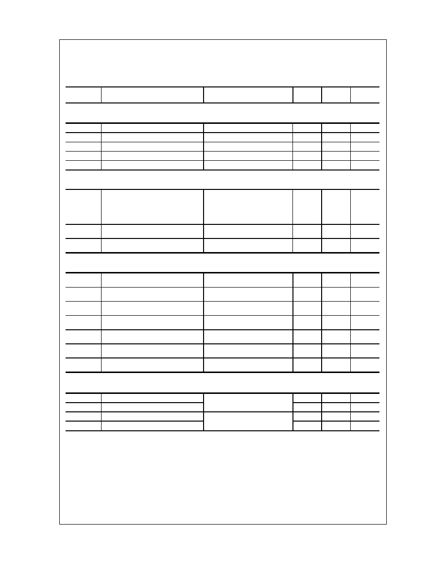
Absolute Maximum Ratings*
TA = 25∞C unless otherwise noted
*
These ratings are limiting values above which the serviceability of any semiconductor device may be impaired.
NOTES:
1) These ratings are based on a maximum junction temperature of 150 degrees C.
2) These are steady state limits. The factory should be consulted on applications involving pulsed or low duty cycle operations.
Symbol
Parameter
Value
Units
V
CEO
Collector-Emitter Voltage
40
V
V
CBO
Collector-Base Voltage
60
V
V
EBO
Emitter-Base Voltage
6.0
V
I
C
Collector Current - Continuous
600 mA
T
J
, T
stg
Operating and Storage Junction Temperature Range
-55 to +150
∞
C
Thermal Characteristics
TA = 25∞C unless otherwise noted
Symbol
Characteristic
Max
Units
2N4401
*MMBT4401
P
D
Total Device Dissipation
Derate above 25
∞
C
625
5.0
350
2.8
mW
mW/
∞
C
R
JC
Thermal Resistance, Junction to Case
83.3
∞
C/W
R
JA
Thermal Resistance, Junction to Ambient
200
357
∞
C/W
C
B E
TO-92
C
B
E
SOT-23
Mark: 2X
*
Device mounted on FR-4 PCB 1.6" X 1.6" X 0.06."
2001 Fairchild Semiconductor
Corporation
2N4401 / MMBT4401
2N4401/MMBT4401, Rev A
3
2N4401 / MMBT4401
Electrical Characteristics
TA = 25∞C unless otherwise noted
OFF CHARACTERISTICS
V
(BR)CEO
Collector-Emitter Breakdown Voltage*
I
C
= 1.0 mA, I
B
= 0
40
V
V
(BR)CBO
Collector-Base Breakdown Voltage
I
C
= 0.1 mA, I
E
= 0
60
V
V
(BR)EBO
Emitter-Base Breakdown Voltage
I
E
= 0.1 mA, I
C
= 0
6.0
V
I
BL
Base Cutoff Current
V
CE
= 35 V, V
EB
= 0.4 V
0.1
µ
A
I
CEX
Collector Cutoff Current
V
CE
= 35 V, V
EB
= 0.4 V
0.1
µ
A
ON CHARACTERISTICS*
h
FE
DC Current Gain
I
C
= 0.1 mA, V
CE
= 1.0 V
I
C
= 1.0 mA, V
CE
= 1.0 V
I
C
= 10 mA, V
CE
= 1.0 V
I
C
= 150 mA, V
CE
= 1.0 V
I
C
= 500 mA, V
CE
= 2.0 V
20
40
80
100
40
300
V
CE(
sat
)
Collector-Emitter Saturation Voltage
I
C
= 150 mA, I
B
= 15 mA
I
C
= 500 mA, I
B
= 50 mA
0.4
0.75
V
V
V
BE(
sat
)
Base-Emitter Saturation Voltage
I
C
= 150 mA, I
B
= 15 mA
I
C
= 500 mA, I
B
= 50 mA
0.75
0.95
1.2
V
V
SMALL SIGNAL CHARACTERISTICS
f
T
Current Gain - Bandwidth Product
I
C
= 20 mA, V
CE
= 10 V,
f = 100 MHz
250
MHz
C
cb
Collector-Base Capacitance
V
CB
= 5.0 V, I
E
= 0,
f = 140 kHz
6.5
pF
C
eb
Emitter-Base Capacitance
V
BE
= 0.5 V, I
C
= 0,
f = 140 kHz
30
pF
h
ie
Input Impedance
I
C
= 1.0 mA, V
CE
= 10 V,
f = 1.0 kHz
1.0
15
k
h
re
Voltage Feedback Ratio
I
C
= 1.0 mA, V
CE
= 10 V,
f = 1.0 kHz
0.1
8.0
x 10
-4
h
fe
Small-Signal Current Gain
I
C
= 1.0 mA, V
CE
= 10 V,
f = 1.0 kHz
40
500
h
oe
Output Admittance
I
C
= 1.0 mA, V
CE
= 10 V,
f = 1.0 kHz
1.0
30
µ
mhos
SWITCHING CHARACTERISTICS
t
d
Delay Time V
CC
= 30 V, V
EB
= 2 V,
15 ns
t
r
Rise Time
I
C
= 150 mA, I
B1
= 15 mA
20
ns
t
s
Storage Time
V
CC
= 30 V, I
C
= 150 mA
225
ns
t
f
Fall Time
I
B1
= I
B2
= 15 mA
30
ns
*
Pulse Test: Pulse Width
300
µ
s, Duty Cycle
2.0%
Symbol
Parameter
Test Conditions
Min
Max
Units
NPN General Purpose Amplifier
(continued)

Typical Characteristics
Typical Pulsed Current Gain
vs Collector Current
0.1
0.3
1
3
10
30
100
300
0
100
200
300
400
500
I - COLLECTOR CURRENT (mA)
h
-
T
Y
P
I
C
A
L
P
U
L
S
E
D
C
U
R
R
E
N
T
GA
IN
C
FE
125 ∞C
25 ∞C
- 40 ∞C
V = 5V
CE
Collector-Emitter Saturation
Voltage vs Collector Current
1
10
100
500
0.1
0.2
0.3
0.4
I - COLLECTOR CURRENT (mA)
V
-
COL
L
E
C
TO
R-
E
M
I
T
T
E
R VOL
T
A
G
E (
V
)
CE
S
A
T
25 ∞C
C
= 10
125 ∞C
- 40 ∞C
Base-Emitter Saturation
Voltage vs Collector Current
1
10
100
500
0.4
0.6
0.8
1
I - COLLECTOR CURRENT (mA)
V
-
B
A
SE-
E
M
I
TTER
VO
L
T
A
G
E
(
V
)
BE
S
A
T
C
= 10
25 ∞C
125 ∞C
- 40 ∞C
Base-Emitter ON Voltage vs
Collector Current
0.1
1
10
25
0.2
0.4
0.6
0.8
1
I - COLLECTOR CURRENT (mA)
V
-
BA
S
E
-
E
M
I
T
T
E
R
ON
V
O
L
T
AG
E
(
V
)
BE
(
O
N
)
C
V = 5V
CE
25 ∞C
125 ∞C
- 40 ∞C
Collector-Cutoff Current
vs Ambient Temperature
25
50
75
100
125
150
0.1
1
10
100
500
T - AMBIENT TEMPERATURE ( C)
I
-
C
O
L
L
E
CT
OR
C
U
R
R
EN
T
(
n
A)
A
V
= 40V
CB
CB
O
∞
Emitter Transition and Output
Capacitance vs Reverse Bias Voltage
0.1
1
10
100
4
8
12
16
20
REVERSE BIAS VOLTAGE (V)
C
A
P
A
CI
T
A
NC
E
(
p
F
)
f = 1 MHz
C ob
C
NPN General Purpose Amplifier
te
(continued)
2N440
1
/
MM
B
T
440
1

Typical Characteristics
(continued)
Power Dissipation vs
Ambient Temperature
0
25
50
75
100
125
150
0
0.25
0.5
0.75
1
TEMPERATURE ( C)
P
-
P
O
W
E
R DIS
S
I
P
A
T
I
O
N (W
)
D
o
SOT-223
TO-92
SOT-23
Turn On and Turn Off Times
vs Collector Current
10
100
1000
0
80
160
240
320
400
I - COLLECTOR CURRENT (mA)
TI
M
E
(
n
S
)
I = I =
t on
t
off
B1
C
B2
I
c
10
V = 25 V
cc
Switching Times
vs Collector Current
10
100
1000
0
80
160
240
320
400
I - COLLECTOR CURRENT (mA)
TI
M
E
(
n
S
)
I = I =
t r
t
s
B1
C
B2
I
c
10
V = 25 V
cc
t f
t d
NPN General Purpose Amplifier
(continued)
2N440
1
/
MM
B
T
440
1

Typical Common Emitter Characteristics
(f = 1.0kHz)
Common Emitter Characteristics
0
10
20
30
40
50
60
0
2
4
6
8
I - COLLECTOR CURRENT (mA)
C
H
A
R
.
R
E
LA
TI
V
E
TO
V
A
L
U
E
S
A
T
I
=
1
0
m
A
V = 10 V
CE
C
C
T = 25 C
A
o
h
oe
h
re
h
fe
h
ie
Common Emitter Characteristics
0
20
40
60
80
100
0
0.4
0.8
1.2
1.6
2
2.4
T - AMBIENT TEMPERATURE ( C)
C
H
A
R
.
R
E
L
A
TI
V
E
TO
V
A
LU
ES
A
T
T
=
2
5
C
V = 10 V
CE
A
A
I = 10 mA
C
h
oe
h
re
h
fe
h
ie
o
o
Common Emitter Characteristics
0
5
10
15
20
25
30
35
0.75
0.8
0.85
0.9
0.95
1
1.05
1.1
1.15
1.2
1.25
1.3
V - COLLECTOR VOLTAGE (V)
CH
A
R
.
R
E
L
A
T
I
VE
TO
V
A
L
U
ES
A
T
V
=
1
0
V
CE
CE
T = 25 C
A
o
h
oe
h
re
h
fe
h
ie
I = 10 mA
C
NPN General Purpose Amplifier
(continued)
2N440
1
/
MM
B
T
440
1