 | –≠–ª–µ–∫—Ç—Ä–æ–Ω–Ω—ã–π –∫–æ–º–ø–æ–Ω–µ–Ω—Ç: 2N5771 | –°–∫–∞—á–∞—Ç—å:  PDF PDF  ZIP ZIP |

2N5771
MMBT5771
PNP Switching Transistor
This device is designed for very high speed saturate switching at
collector currents to 100 mA. Sourced from Process 65. See
PN4258 for characteristics.
2N5771 / MMBT5771
Absolute Maximum Ratings*
TA = 25∞C unless otherwise noted
*
These ratings are limiting values above which the serviceability of any semiconductor device may be impaired.
NOTES:
1) These ratings are based on a maximum junction temperature of 150 degrees C.
2) These are steady state limits. The factory should be consulted on applications involving pulsed or low duty cycle operations.
Thermal Characteristics
TA = 25∞C unless otherwise noted
Symbol
Parameter
Value
Units
V
CEO
Collector-Emitter Voltage
15
V
V
CBO
Collector-Base Voltage
15
V
V
EBO
Emitter-Base Voltage
4.5
V
I
C
Collector Current - Continuous
200
mA
T
J
, T
stg
Operating and Storage Junction Temperature Range
-55 to +150
∞
C
Symbol
Characteristic
Max
Units
2N5771
*MMBT5771
P
D
Total Device Dissipation
Derate above 25
∞
C
350
2.8
225
1.8
mW
mW/
∞
C
R
JC
Thermal Resistance, Junction to Case
125
∞
C/W
R
JA
Thermal Resistance, Junction to Ambient
357
556
∞
C/W
C
B
E
TO-92
C
B
E
SOT-23
Mark: 3R
*
Device mounted on FR-4 PCB 1.6" X 1.6" X 0.06."
Discrete POWER & Signal
Technologies
©
1997 Fairchild Semiconductor Corporation
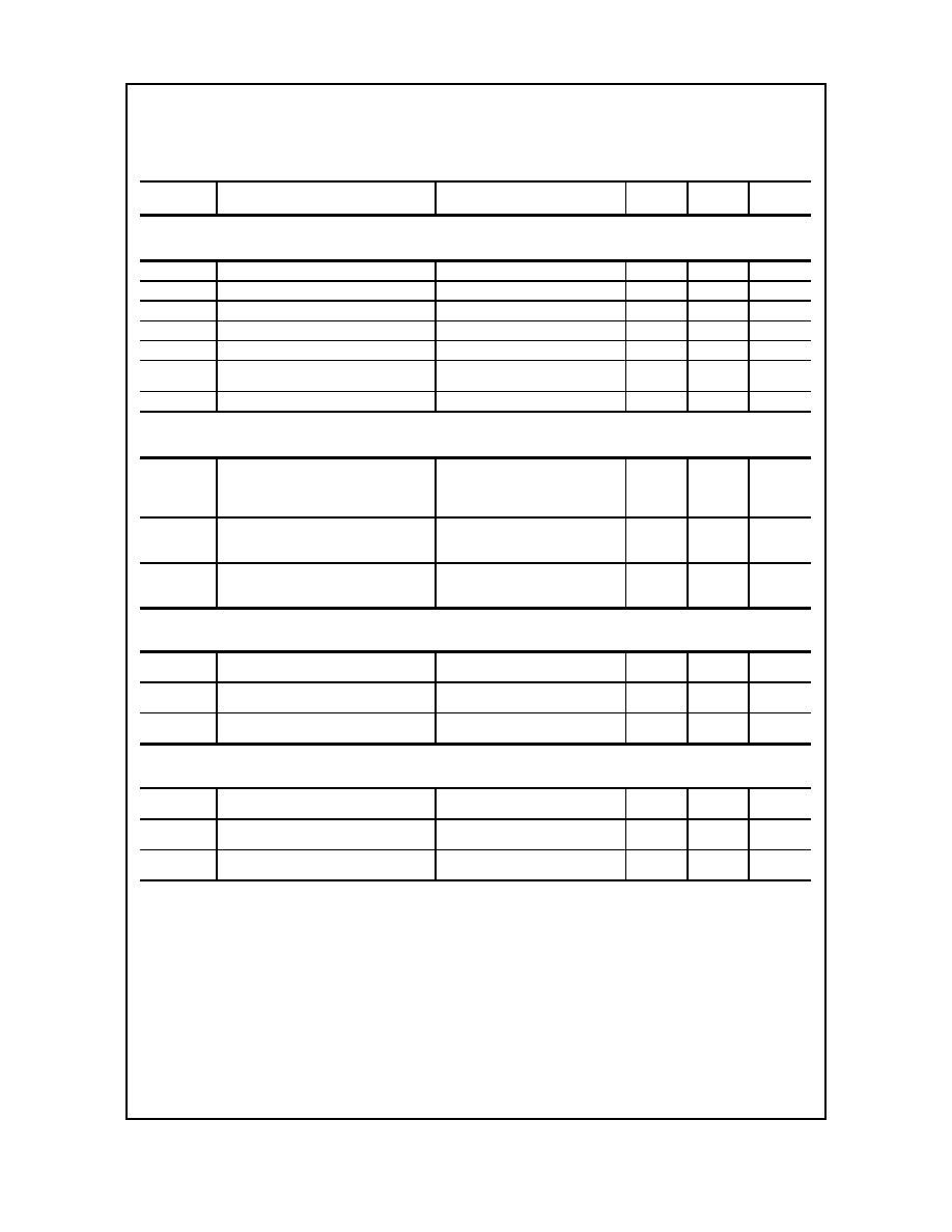
Electrical Characteristics
TA = 25∞C unless otherwise noted
OFF CHARACTERISTICS
Symbol
Parameter
Test Conditions
Min
Max
Units
V
(BR)CEO
Collector-Emitter Breakdown Voltage*
I
C
= 3.0 mA, I
B
= 0
15
V
V
(BR)CES
Collector-Emitter Breakdown Voltage
I
C
= 100
µ
A, V
BE
= 0
15
V
V
(BR)CBO
Collector-Base Breakdown Voltage
I
C
= 100
µ
A, I
E
= 0
15
V
V
(BR)EBO
Emitter-Base Breakdown Voltage
I
E
= 100
µ
A, I
C
= 0
4.5
V
I
CBO
Collector Cutoff Current
V
CB
= 8.0 V, I
E
= 0
10
nA
I
CES
Collector Cutoff Current
V
CE
= 8.0 V, V
BE
= 0
V
CE
= 8.0 V, V
BE
= 0, T
A
= 125
∞
C
10
5.0
nA
µ
A
I
EBO
Emitter Cutoff Current
V
EB
= 4.5 V, I
C
= 0
1.0
µ
A
SMALL SIGNAL CHARACTERISTICS
ON CHARACTERISTICS*
h
FE
DC Current Gain
I
C
= 1.0 mA, V
CE
= 0.5 V
I
C
= 10 mA, V
CE
= 0.3 V
I
C
= 10mA,V
CE
= 0.3V,T
A
= -55
∞
C
I
C
= 50 mA, V
CE
= 1.0 V
35
50
20
40
120
V
CE(
sat
)
Collector-Emitter Saturation Voltage
I
C
= 1.0 mA, I
B
= 0.1 mA
I
C
= 10 mA, I
B
= 1.0 mA
I
C
= 50 mA, I
B
= 5.0 mA
0.15
0.18
0.6
V
V
V
V
BE(
sat
)
Base-Emitter Saturation Voltage
I
C
= 1.0 mA, I
B
= 0.1 mA
I
C
= 10 mA, I
B
= 1.0 mA
I
C
= 50 mA, I
B
= 5.0 mA
0.75
0.8
0.95
1.5
V
V
V
C
cb
Collector-Base Capacitance
V
CB
= 5.0 V, I
E
= 0,
f = 140 kHz
3.0
pF
C
eb
Emitter-Base Capacitance
V
BE
= 0.5 V, I
C
= 0,
f = 140 kHz
3.5
pF
h
fe
Small-Signal Current Gain
I
C
= 10 mA, V
CE
= 10 V,
f = 100 MHz
8.5
MHz
SWITCHING CHARACTERISTICS
t
s
Storage Time
I
C
= 10 mA, V
CC
= 1.5 V,
I
B1
= I
B2
= 1.0 mA
20
ns
t
on
Turn-On Time
I
C
= 10 mA, V
CC
= 1.5 V,
I
B
= 1.0 mA
15
ns
t
off
Turn-Off Time
I
C
= 10 mA, V
CC
= 1.5 V,
I
B1
= I
B2
= 1.0 mA
20
ns
PNP Switching Transistor
(continued)
*
Pulse Test: Pulse Width
300
µ
s, Duty Cycle
2.0%
2N5771 / MMBT5771

N
Discrete POWER & Signal
Technologies
NPN Darlington Transistor
This device is designed for applications requiring extremely
high current gain at collector currents to 1.0 A. Sourced from
Process 05. See MPSA14 for characteristics.
2N6427
MMBT6427
Absolute Maximum Ratings*
TA = 25∞C unless otherwise noted
*
These ratings are limiting values above which the serviceability of any semiconductor device may be impaired.
NOTES:
1) These ratings are based on a maximum junction temperature of 150 degrees C.
2) These are steady state limits. The factory should be consulted on applications involving pulsed or low duty cycle operations.
Symbol
Parameter
Value
Units
V
CEO
Collector-Emitter Voltage
40
V
V
CBO
Collector-Base Voltage
40
V
V
EBO
Emitter-Base Voltage
12
V
I
C
Collector Current - Continuous
1.2
A
T
J
, T
stg
Operating and Storage Junction Temperature Range
-55 to +150
∞
C
Thermal Characteristics
TA = 25∞C unless otherwise noted
Symbol
Characteristic
Max
Units
2N6427
*MMBT6427
P
D
Total Device Dissipation
Derate above 25
∞
C
625
5.0
350
2.8
mW
mW/
∞
C
R
JC
Thermal Resistance, Junction to Case
83.3
∞
C/W
R
JA
Thermal Resistance, Junction to Ambient
200
357
∞
C/W
2N6427 / MMBT6427
C
B
E
TO-92
C
B
E
SOT-23
Mark: 1V
*
Device mounted on FR-4 PCB 1.6" X 1.6" X 0.06."
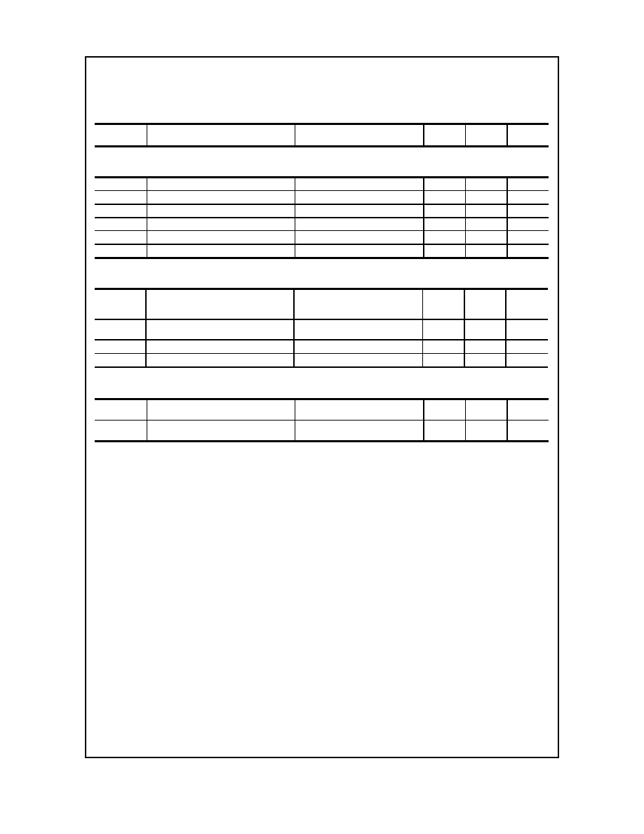
Electrical Characteristics
TA = 25∞C unless otherwise noted
OFF CHARACTERISTICS
ON CHARACTERISTICS
V
(BR)CEO
Collector-Emitter Breakdown Voltage*
I
C
= 10 mA, I
B
= 0
40
V
V
(BR)CBO
Collector-Base Breakdown Voltage
I
C
= 100
µ
A, I
E
= 0
40
V
V
(BR)EBO
Emitter-Base Breakdown Voltage
I
E
= 10
µ
A, I
C
= 0
12
V
I
CEO
Collector Cutoff Current
V
CE
= 25 V, I
B
= 0
1.0
µ
A
I
CBO
Collector Cutoff Current
V
CB
= 30 V, I
E
= 0
50
nA
I
EBO
Emitter Cutoff Current
V
EB
= 10 V, I
C
= 0
50
nA
SMALL SIGNAL CHARACTERISTICS
C
obo
Output Capacitance
V
CB
= 10 V, I
E
= 0,
f = 1.0 MHz
7.0
pF
C
ibo
Input Capcitance
V
BE
= 1.0 V, I
C
= 0,
f = 1.0 MHz
15
pF
*
Pulse Test: Pulse Width
300
µ
s, Duty Cycle
2.0%
h
FE
DC Current Gain*
I
C
= 10 mA, V
CE
= 5.0 V
I
C
= 100 mA, V
CE
= 5.0 V
I
C
= 500 mA, V
CE
= 5.0 V
10,000
20,000
14,000
100,000
200,000
140,000
V
CE(
sat
)
Collector-Emitter Saturation Voltage
I
C
= 50 mA, I
B
= 0.5 mA
I
C
= 500 mA, I
B
= 0.5 mA
1.2
1.5
V
V
V
BE(
sat
)
Base-Emitter Saturation Voltage
I
C
= 500 mA, I
B
= 0.5 mA
2.0
V
V
BE(
on
)
Base-Emitter On Voltage
I
C
= 50 mA, V
CE
= 5.0 mA
1.75
V
NPN Darlington Transistor
(continued)
Symbol
Parameter
Test Conditions
Min
Max
Units
2N6427 / MMBT6427