 | –≠–ª–µ–∫—Ç—Ä–æ–Ω–Ω—ã–π –∫–æ–º–ø–æ–Ω–µ–Ω—Ç: 2N7002-T1 | –°–∫–∞—á–∞—Ç—å:  PDF PDF  ZIP ZIP |
2N7000/7002, VQ1000J/P, BS170
Siliconix
S-52429--Rev. E, 28-Apr-97
1
N-Channel Enhancement-Mode MOSFET Transistors
Product Summary
Part Number
V
(BR)DSS
Min (V)
r
DS(on)
Max (
W)
V
GS(th)
(V)
I
D
(A)
2N7000
5 @ V
GS
= 10 V
0.8 to 3
0.2
2N7002
7.5 @ V
GS
= 10 V
1 to 2.5
0.115
VQ1000J
60
5.5 @ V
GS
= 10 V
0.8 to 2.5
0.225
VQ1000P
5.5 @ V
GS
= 10 V
0.8 to 2.5
0.225
BS170
5 @ V
GS
= 10 V
0.8 to 3
0.5
Features
Benefits
Applications
D Low On-Resistance: 2.5 W
D Low Threshold: 2.1 V
D Low Input Capacitance: 22 pF
D Fast Switching Speed: 7 ns
D Low Input and Output Leakage
D Low Offset Voltage
D Low-Voltage Operation
D Easily Driven Without Buffer
D High-Speed Circuits
D Low Error Voltage
D Direct Logic-Level Interface: TTL/CMOS
D Drivers: Relays, Solenoids, Lamps, Hammers,
Displays, Memories, Transistors, etc.
D Battery Operated Systems
D Solid-State Relays
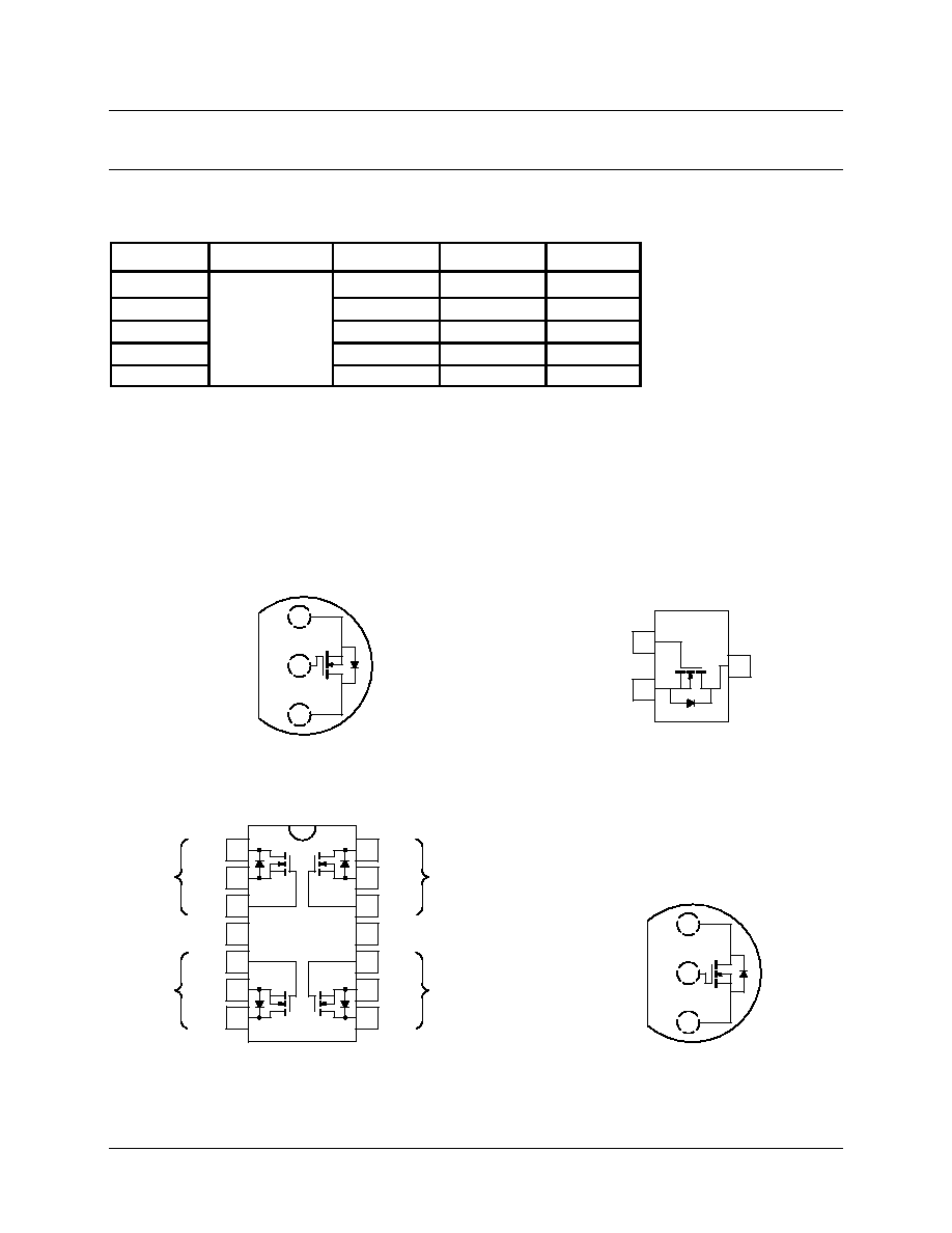
2N7002 (72)*
*Marking Code for TO-236
TO-226AA
(TO-92)
Top View
S
D
G
1
2
3
G
TO-236
(SOT-23)
S
D
Top View
2
3
1
Plastic: VQ1000J
Sidebraze: VQ1000P
Top View
TO-92-18RM
(TO-18 Lead Form)
D
S
G
1
2
3
2N7000
BS170
1
2
3
4
5
6
7
14
13
12
11
10
9
8
Top View
Dual-In-Line
D
1
D
4
S
1
S
4
G
1
G
4
NC
NC
G
2
G
3
S
2
S
3
D
2
D
3
N
N
N
N
Updates to this data sheet may be obtained via facsimile by calling Siliconix FaxBack, 1-408-970-5600. Please request FaxBack document #70226.

2N7000/7002, VQ1000J/P, BS170
2
Siliconix
S-52429--Rev. E, 28-Apr-97
Absolute Maximum Ratings (T
A
= 25
_C Unless Otherwise Noted)
Single
Total
Quad
Parameter
Symbol
2N7000
2N7002
VQ1000J
VQ1000P
VQ1000J/P
BS170
Unit
Drain-Source Voltage
V
DS
60
60
60
60
60
Gate-Source Voltage--Non-Repetitive
V
GSM
"40
"40
"30
"25
V
Gate-Source Voltage--Continuous
V
GS
"20
"20
"20
"20
"20
Continuous Drain Current
T
A
= 25
_C
I
D
0.2
0.115
0.225
0.225
0.5
(T
J
= 150
_C)
T
A
= 100
_C
I
D
0.13
0.073
0.14
0.14
0.175
A
Pulsed Drain Current
a
I
DM
0.5
0.8
1
1
Power Dissipation
T
A
= 25
_C
P
D
0.4
0.2
1.3
1.3
2
0.83
W
Power Dissipation
T
A
= 100
_C
P
D
0.16
0.08
0.52
0.52
0.8
W
Maximum Junction-to-Ambient
R
thJA
312.5
625
96
96
62.5
156
_C/W
Operating Junction and
Storage Temperature Range
T
J
, T
stg
≠55 to 150
_C
Notes
a.
Pulse width limited by maximum junction temperature.
b.
t
p
v 50 ms.
Specifications
a
for 2N7000 and 2N7002
Limits
2N7000
2N7002
Parameter
Symbol
Test Conditions
Typ
b
Min
Max
Min
Max
Unit
Static
Drain-Source Breakdown Voltage
V
(BR)DSS
V
GS
= 0 V, I
D
= 10
mA
70
60
60
Gate Threshold Voltage
V
GS(th)
V
DS
= V
GS
, I
D
= 1 mA
2.1
0.8
3
V
Gate-Threshold Voltage
V
GS(th)
V
DS
= V
GS
, I
D
= 0.25 mA
2.0
1
2.5
V
DS
= 0 V, V
GS
=
"15 V
"10
Gate-Body Leakage
I
GSS
V
DS
= 0 V, V
GS
=
"20 V
"10
0
nA
V
DS
= 48 V, V
GS
= 0 V
1
Zero Gate Voltage Drain Current
I
DSS
T
C
= 125
_C
1000
mA
Zero Gate Voltage Drain Current
I
DSS
V
DS
= 60 V, V
GS
= 0 V
1
mA
T
C
= 125
_C
500
On State Drain Current
c
I
D(
)
V
DS
= 10 V, V
GS
= 4.5 V
0.35
0.075
A
On-State Drain Current
c
I
D(on)
V
DS
= 7.5 V, V
GS
= 10 V
1
0.5
A
V
GS
= 4.5 V, I
D
= 0.075 A
4.5
5.3
V
GS
= 5 V, I
D
= 0.05 A
3.2
7.5
Drain-Source On-Resistance
c
r
DS(on)
T
C
= 125
_C
5.8
13.5
W
V
GS
= 10 V, I
D
= 0.5 A
2.4
5
7.5
T
J
= 125
_C
4.4
9
13.5
Forward Transconductance
c
g
fs
V
DS
= 10 V, I
D
= 0.2 A
100
80
mS
Common Source Output Conductance
c
g
os
V
DS
= 5 V, I
D
= 0.05 A
0.5
mS
Dynamic
Input Capacitance
C
iss
V
25 V V
0 V
22
60
50
Output Capacitance
C
oss
V
DS
= 25 V, V
GS
= 0 V
f = 1 MHz
11
25
25
pF
Reverse Transfer Capacitance
C
rss
f 1 MHz
2
5
5

2N7000/7002, VQ1000J/P, BS170
Siliconix
S-52429--Rev. E, 28-Apr-97
3
Specifications
a
for 2N7000 and 2N7002
Limits
2N7000
2N7002
Parameter
Symbol
Test Conditions
Typ
b
Min
Max
Min
Max
Unit
Switching
e
Turn-On Time
t
ON
V
DD
= 15 V, R
L
= 25 W
I
D
^0 5 A V
GEN
= 10 V
7
10
Turn-Off Time
t
OFF
I
D
^0.5 A, V
GEN
= 10 V
R
G
= 25 W
7
10
ns
Turn-On Time
t
ON
V
DD
= 30 V, R
L
= 150 W
I
D
^ 0 2 A V
GEN
= 10 V
7
20
ns
Turn-Off Time
t
OFF
I
D
^ 0.2 A, V
GEN
= 10 V
R
G
= 25 W
11
20
Notes
a.
T
A
= 25
_C unless otherwise noted.d.
VNBF06
b.
For DESIGN AID ONLY, not subject to production testing.
c.
Pulse test: PW
v80 ms duty cycle v1%.
d.
This parameter not registered with JEDEC.
e.
Switching time is essentially independent of operating temperature.
Specifications
a
for VQ1000J/P and BS170
Limits
VQ1000J/P
BS170
Parameter
Symbol
Test Conditions
Typ
b
Min
Max
Min
Max
Unit
Static
Drain-Source Breakdown Voltage
V
(BR)DSS
V
GS
= 0 V, I
D
= 100
mA
70
60
60
V
Gate-Threshold Voltage
V
GS(th)
V
DS
= V
GS
, I
D
= 1 mA
2.1
0.8
2.5
0.8
3
V
V
DS
= 0 V, V
GS
=
"10 V
"100
Gate-Body Leakage
I
GSS
T
J
= 125
_C
"500
nA
V
DS
= 0 V, V
GS
=
"15 V
"10
V
DS
= 25 V, V
GS
= 0 V
0.5
Zero Gate Voltage Drain Current
I
DSS
V
DS
= 48 V, V
GS
= 0 V,
T
J
= 125
_C
500
mA
V
DS
= 60 V, V
GS
= 0 V
10
On-State Drain Current
c
I
D(on)
V
DS
= 10 V, V
GS
=
10 V
1
0.5
A
V
GS
= 5 V, I
D
=
0.2 A
4
7.5
Drain Source On Resistance
c
r
DS(
)
V
GS
=
10 V, I
D
=
0.2 A
2.3
5
W
Drain-Source On-Resistance
c
r
DS(on)
V
GS
=
10 V, I
D
=
0.3 A
2.3
5.5
W
T
J
= 125
_C
4.2
7.6
Forward Transconductance
c
g
f
V
DS
= 10 V, I
D
=
0.2 A
100
Forward Transconductance
c
g
fs
V
DS
= 10 V, I
D
=
0.5 A
100
mS
Common Source Output Conductance
c
g
os
V
DS
=5 V, I
D
= 0.05 A
0.5
Dynamic
Input Capacitance
C
iss
V
25 V V
0 V
22
60
60
Output Capacitance
C
oss
V
DS
=25 V, V
GS
= 0 V
f = 1 MHz
11
25
pF
Reverse Transfer Capacitance
C
rss
f 1 MHz
2
5
2N7000/7002, VQ1000J/P, BS170
4
Siliconix
S-52429--Rev. E, 28-Apr-97
Specifications
a
for VQ1000J/P and BS170
Limits
VQ1000J/P
BS170
Parameter
Symbol
Test Conditions
Typ
b
Min
Max
Min
Max
Unit
Switching
d
Turn-On Time
t
ON
V
DD
= 15 V, R
L
= 23 W
I
D
^ 0 6 A V
GEN
= 10 V
7
10
Turn-Off Time
t
OFF
I
D
^ 0.6 A, V
GEN
= 10 V
R
G
= 25 W
7
10
ns
Turn-On Time
t
ON
V
DD
= 25 V, R
L
= 125 W
I
D
^ 0 2 A V
GEN
= 10 V
7
10
ns
Turn-Off Time
t
OFF
I
D
^ 0.2 A, V
GEN
= 10 V
R
G
= 25 W
7
10
Notes
a.
T
A
= 25
_C unless otherwise noted.
VNBF06
b.
For DESIGN AID ONLY, not subject to production testing.
c.
Pulse test: PW
v80 ms duty cycle v1%.
d.
Switching time is essentially independent of operating temperature.
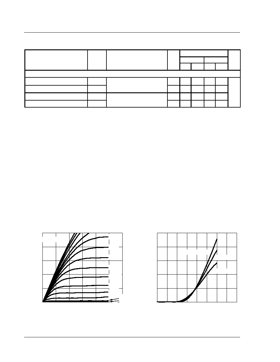
Typical Characteristics (25
_C Unless Otherwise Noted)
0
0.2
0.4
0.6
0.8
1.0
0
1
2
3
4
5
6
0
0.2
0.4
0.6
0.8
1.0
0
1
2
3
4
5
6
7
8
Output Characteristics
Transfer Characteristics
V
DS
≠ Drain-to-Source Voltage (V)
≠ Drain Current (A)
I
D
V
GS
= 10, 9, 8, 7 V
6.5 V
V
GS
≠ Gate-to-Source Voltage (V)
≠ Drain Current (A)
I
D
T
A
= ≠55
_C
25
_C
125
_C
6 V
5.5 V
5 V
4.5 V
4 V
3.5 V
3 V
2.5 V
2, 1 V

2N7000/7002, VQ1000J/P, BS170
Siliconix
S-52429--Rev. E, 28-Apr-97
5
Typical Characteristics (25
_C Unless Otherwise Noted)
0
4
8
12
16
20
0
400
800
1200
1600
2000
2400
0
0.5
1.0
1.5
2.0
≠55
≠30
≠5
20
45
70
95
120
145
0
1
2
3
4
5
6
7
0
0.2
0.4
0.6
0.8
1.0
0
10
20
30
40
50
60
0
5
10
15
20
25
30
35
Gate Charge
On-Resistance vs. Drain Current
≠ Gate-to-Source
V
oltage (V)
Q
g
≠ Total Gate Charge (pC)
V
DS
≠ Drain-to-Source Voltage (V)
C ≠ Capacitance (pF)
V
GS
C
rss
C
oss
C
iss
V
DS
= 30 V
I
D
= 0.5 A
≠ On-Resistance (
r
DS(on)
I
D
≠ Drain Current (A)
Capacitance
On-Resistance vs. Junction Temperature
V
GS
= 10 V, r
DS
@ 0.5 A
T
J
≠ Junction Temperature (
_
C)
(Normalized)
≠ On-Resistance (
r
DS(on)
r
DS
@ 10 V = V
GS
r
DS
@ 5 V = V
GS
T
J
= 25
_C
V
GS
= 5 V, r
DS
@ 0.05 A
V
GS
= 0 V
f = 1 MHz
0.001
0.010
0.100
1.000
0
0.2
0.4
0.6
0.8
1.0
1.2
1.4
Source-Drain Diode Forward Voltage
On-Resistance vs. Gate-to-Source Voltage
≠ On-Resistance (
r
DS(on)
V
SD
≠ Source-to-Drain Voltage (V)
V
GS
≠ Gate-to-Source Voltage (V)
≠ Source Current (A)
I
S
0
1
2
3
4
5
6
0
2
4
6
8
10
12
14
16
18
20
500 mA
r
DS
= 50 mA
W
)
W
)
W
)
T
J
= 25
_C
T
J
= 125
_C

2N7000/7002, VQ1000J/P, BS170
6
Siliconix
S-52429--Rev. E, 28-Apr-97
Typical Characteristics (25
_C Unless Otherwise Noted)
Threshold Voltage
T
J
≠ Temperature (
_C)
≠0.75
≠0.50
≠0.25
≠0.00
0.25
0.50
≠50
≠25
0
25
50
75
100
125
150
I
D
= 250
mA
V
ariance (V)
V
GS(th)
10 K
Duty Cycle = 0.5
0.2
0.1
0.05
0.02
Single Pulse
1
0.01
0.1
0.01
0.1
1
100
10
1 K
Normalized Effective Transient Thermal Impedance, Junction-to-Ambient (TO-226AA, BS170 Only)
Normalized Ef
fective
T
ransient
Thermal Impedance
t
1
≠ Square Wave Pulse Duration (sec)
1. Duty Cycle, D =
2. Per Unit Base = R
thJA
= 156
_
C/W
3. T
JM
≠ T
A
= P
DM
Z
thJA
(t)
t
1
t
2
t
1
Notes:
P
DM
t
2