© 2002 Fairchild Semiconductor Corporation
DS005939
www.fairchildsemi.com
October 1987
Revised March 2002
CD400
1BC
/
CD401
1BC
Quad 2-
Input
NOR B
u
f
f
e
r
ed B
Ser
i
es Gate ∑
Quad 2-I
nput
NAND
Buf
f
er
ed B
Seri
es G
a
te
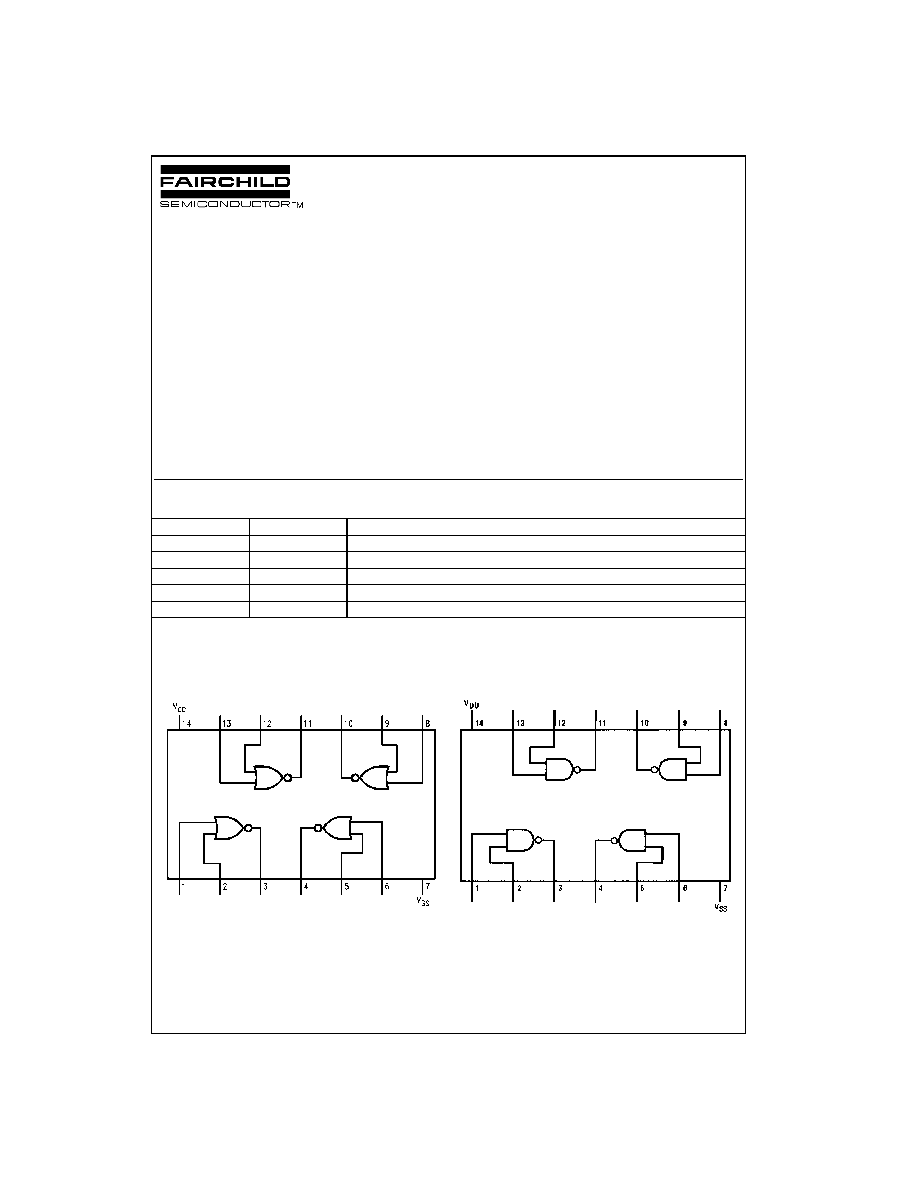
CD4001BC/CD4011BC
Quad 2-Input NOR Buffered B Series Gate ∑
Quad 2-Input NAND Buffered B Series Gate
General Description
The CD4001BC and CD4011BC quad gates are monolithic
complementary MOS (CMOS) integrated circuits con-
structed with N- and P-channel enhancement mode tran-
sistors. They have equal source and sink current
capabilities and conform to standard B series output drive.
The devices also have buffered outputs which improve
transfer characteristics by providing very high gain.
All inputs are protected against static discharge with diodes
to V
DD
and V
SS
.
Features
s
Low power TTL:
Fan out of 2 driving 74L compatibility:
or 1 driving 74LS
s
5V≠10V≠15V parametric ratings
s
Symmetrical output characteristics
s
Maximum input leakage 1
µ
A at 15V over full
temperature range
Ordering Code:
Devices also available in Tape and Reel. Specify by appending the suffix letter "X" to the ordering code.
Connection Diagrams
Pin Assignments for DIP, SOIC and SOP
CD4001BC
Top View
Pin Assignments for DIP and SOIC
CD4011BC
Top View
Order Number
Package Number
Package Description
CD4001BCM
M14A
14-Lead Small Outline Integrated Circuit (SOIC), JEDEC MS-012, 0.150" Narrow
CD4001BCSJ
M14D
14-Lead Small Outline Package (SOP), EIAJ TYPE II, 5.3mm Wide
CD4001BCN
N14A
14-Lead Plastic Dual-In-Line Package (PDIP), JEDEC MS-001, 0.300" Wide
CD4011BCM
M14A
14-Lead Small Outline Integrated Circuit (SOIC), JEDEC MS-012, 0.150" Narrow
CD4011BCN
N14A
14-Lead Plastic Dual-In-Line Package (PDIP), JEDEC MS-001, 0.300" Wide
3
www.fairchildsemi.com
CD400
1BC
/
CD401
1BC
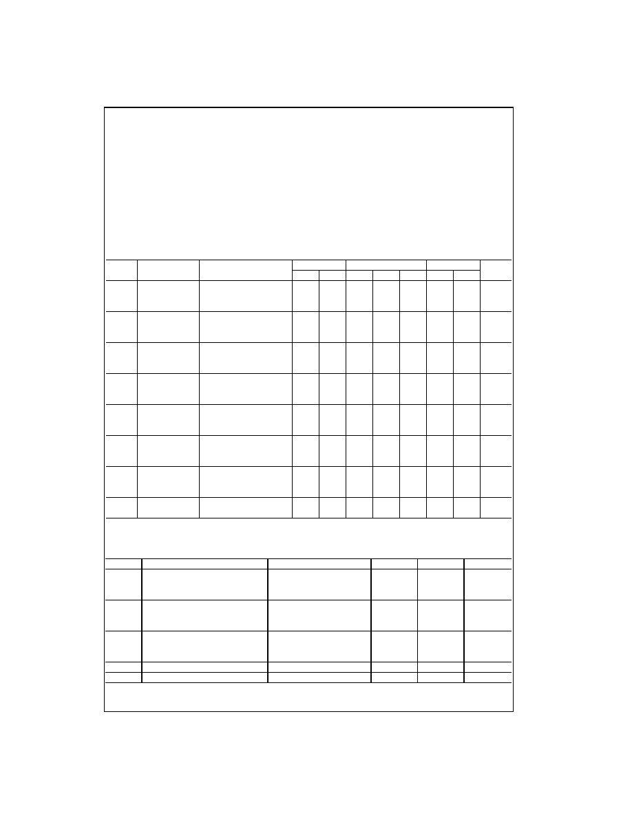
Absolute Maximum Ratings
(Note 1)
(Note 2)
Recommended Operating
Conditions
Note 1: "Absolute Maximum Ratings" are those values beyond which the
safety of the device cannot be guaranteed. Except for "Operating Tempera-
ture Range" they are not meant to imply that the devices should be oper-
ated at these limits. The Electrical Characteristics tables provide conditions
for actual device operation.
Note 2: All voltages measured with respect to V
SS
unless otherwise speci-
fied.
DC Electrical Characteristics
(Note 2)
Note 3: I
OL
and I
OH
are tested one output at a time.
AC Electrical Characteristics
(Note 4)
CD4001BC: T
A
=
25
∞
C, Input t
r
; t
f
=
20 ns. C
L
=
50 pF, R
L
=
200k. Typical temperature coefficient is 0.3%/
∞
C.
Note 4: AC Parameters are guaranteed by DC correlated testing.
Voltage at any Pin
-
0.5V to V
DD
+
0.5V
Power Dissipation (P
D
)
Dual-In-Line
700 mW
Small Outline
500 mW
V
DD
Range
-
0.5 V
DC
to
+
18 V
DC
Storage Temperature (T
S
)
-
65
∞
C to
+
150
∞
C
Lead Temperature (T
L
)
(Soldering, 10 seconds)
260
∞
C
Operating Range (V
DD
)
3 V
DC
to 15 V
DC
Operating Temperature Range
CD4001BC, CD4011BC
-
55
∞
C to
+
125
∞
C
Symbol
Parameter
Conditions
-
55
∞
C
+
25
∞
C
+
125
∞
C
Units
Min
Max
Min
Typ
Max
Min
Max
I
DD
Quiescent Device
V
DD
=
5V, V
IN
=
V
DD
or V
SS
0.25
0.004
0.25
7.5
µ
A
Current
V
DD
=
10V, V
IN
=
V
DD
or V
SS
0.5
0.005
0.50
15
V
DD
=
15V, V
IN
=
V
DD
or V
SS
1.0
0.006
1.0
30
V
OL
LOW Level
V
DD
=
5V
0.05
0
0.05
0.05
V
Output Voltage
V
DD
=
10V
|I
O
|
<
1
µ
A
0.05
0
0.05
0.05
V
DD
=
15V
0.05
0
0.05
0.05
V
OH
HIGH Level
V
DD
=
5V
4.95
4.95
5
4.95
V
Output Voltage
V
DD
=
10V
|I
O
|
<
1
µ
A
9.95
9.95
10
9.95
V
DD
=
15V
14.95
14.95
15
14.95
V
IL
LOW Level
V
DD
=
5V, V
O
=
4.5V
1.5
2
1.5
1.5
V
Input Voltage
V
DD
=
10V, V
O
=
9.0V
3.0
4
3.0
3.0
V
DD
=
15V, V
O
=
13.5V
4.0
6
4.0
4.0
V
IH
HIGH Level
V
DD
=
5V, V
O
=
0.5V
3.5
3.5
3
3.5
V
Input Voltage
V
DD
=
10V, V
O
=
1.0V
7.0
7.0
6
7.0
V
DD
=
15V, V
O
=
1.5V
11.0
11.0
9
11.0
I
OL
LOW Level Output
V
DD
=
5V, V
O
=
0.4V
0.64
0.51
0.88
0.36
mA
Current
V
DD
=
10V, V
O
=
0.5V
1.6
1.3
2.25
0.9
(Note 3)
V
DD
=
15V, V
O
=
1.5V
4.2
3.4
8.8
2.4
I
OH
HIGH Level Output
V
DD
=
5V, V
O
=
4.6V
-
0.64
-
0.51
-
0.88
-
0.36
mA
Current
V
DD
=
10V, V
O
=
9.5V
-
1.6
-
1.3
-
2.25
-
0.9
(Note 3)
V
DD
=
15V, V
O
=
13.5V
-
4.2
-
3.4
-
8.8
-
2.4
I
IN
Input Current
V
DD
=
15V, V
IN
=
0V
-
0.10
-
10
-
5
-
0.10
-
1.0
µ
A
V
DD
=
15V, V
IN
=
15V
0.1
10
-
5
0.10
1.0
Symbol
Parameter
Conditions
Typ
Max
Units
t
PHL
Propagation Delay Time,
V
DD
=
5V
120
250
ns
HIGH-to-LOW Level
V
DD
=
10V
50
100
V
DD
=
15V
35
70
t
PLH
Propagation Delay Time,
V
DD
=
5V
110
250
ns
LOW-to-HIGH Level
V
DD
=
10V
50
100
V
DD
=
15V
35
70
t
THL
, t
TLH
Transition Time
V
DD
=
5V
90
200
ns
V
DD
=
10V
50
100
V
DD
=
15V
40
80
C
IN
Average Input Capacitance
Any Input
5
7.5
pF
C
PD
Power Dissipation Capacity
Any Gate
14
pF

www.fairchildsemi.com
4
CD4001BC/
C
D
40
1
1
BC
AC Electrical Characteristics
(Note 5)
CD4011BC: T
A
=
25
∞
C, Input t
r
; t
f
=
20 ns. C
L
=
50 pF, R
L
=
200k. Typical Temperature Coefficient is 0.3%/
∞
C.
Note 5: AC Parameters are guaranteed by DC correlated testing.
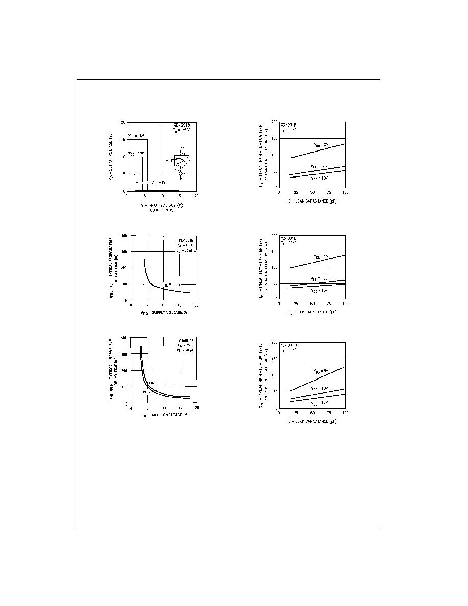
Typical Performance Characteristics
Typical
Transfer Characteristics
Typical
Transfer Characteristics
Typical
Transfer Characteristics
Symbol
Parameter
Conditions
Typ
Max
Units
t
PHL
Propagation Delay,
V
DD
=
5V
120
250
ns
HIGH-to-LOW Level
V
DD
=
10V
50
100
V
DD
=
15V
35
70
t
PLH
Propagation Delay,
V
DD
=
5V
85
250
ns
LOW-to-HIGH Level
V
DD
=
10V
40
100
V
DD
=
15V
30
70
t
THL
, t
TLH
Transition Time
V
DD
=
5V
90
200
ns
V
DD
=
10V
50
100
V
DD
=
15V
40
80
C
IN
Average Input Capacitance
Any Input
5
7.5
pF
C
PD
Power Dissipation Capacity
Any Gate
14
pF