 | –≠–ª–µ–∫—Ç—Ä–æ–Ω–Ω—ã–π –∫–æ–º–ø–æ–Ω–µ–Ω—Ç: 5M0365R | –°–∫–∞—á–∞—Ç—å:  PDF PDF  ZIP ZIP |
©2002 Fairchild Semiconductor Corporation
www.fairchildsemi.com
Rev.1.0.5
Features
∑ Precision Fixed Operating Frequency (100/67/50kHz)
∑ Low Start-up Current(Typ. 100uA)
∑ Pulse by Pulse Current Limiting
∑ Over Current Protection
∑ Over Voltage Protection (Min. 25V)
∑ Internal Thermal Shutdown Function
∑ Under Voltage Lockout
∑ Internal High Voltage Sense FET
∑ Auto-Restart Mode
Applications
∑ SMPS for VCR, SVR, STB, DVD & DVCD
∑ SMPS for Printer, Facsimile & Scanner
∑ Adaptor for Camcorder
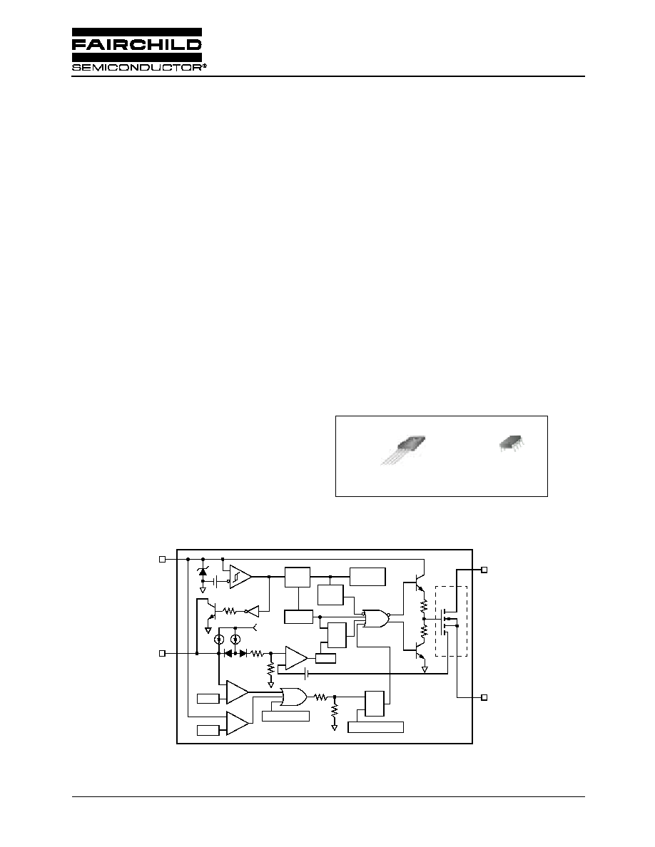
Description
The Fairchild Power Switch(FPS) product family is specially
designed for an off-line SMPS with minimal external
components. The Fairchild Power Switch(FPS) consists of a
high voltage power SenseFET and a current mode PWM IC.
Included PWM controller integrates the fixed frequency
oscillator, the under voltage lock-out, the leading edge
blanking, the optimized gate turn-on/turn-off driver, the
thermal shutdown protection, the over voltage protection,
and the temperature compensated precision current sources
for the loop compensation and the fault protection circuitry.
Compared to a discrete MOSFET and a PWM controller or
an RCCsolution, a Fairchild Power Switch(FPS) can reduce
the total component count, design size and weight and at the
same time increase efficiency, productivity, and system
reliability. It has a basic platform well suited for the cost
effective design in either a flyback converter or a forward
converter
Internal Block Diagram
#3 V
CC
32V
5
µ
A
9V
2.5R
1R
1mA
0.1V
+
-
OVER VOLTAGE S/D
+
-
7.5V
27V
Thermal S/D
S
R
Q
Power on reset
+
-
L.E.B
S
R
Q
OSC
5V
Vref
Internal
bias
Good
logic
SFET
#2 DRAIN
#1 GND
#4 FB
(*#3 V
CC
)
(*#4 FB)
(*#1.6.7.8 DRAIN)
(*#2 GND)
*Asterisk - KA5M0365RN, KA5L0365RN
KA5x03xx-SERIES
KA5H0365R, KA5M0365R, KA5L0365R, KA5M0365RN,
KA5L0365RN, KA5H0380R, KA5M0380R, KA5L0380R
Fairchild Power Switch(FPS)
TO-220F-4L
1. GND 2. Drain 3. V
CC
4. FB
1
8-DIP
1.6.7.8 Drain
2. GND
3. V
CC
4. FB 5. NC

KA5X03XX-SERIES
2
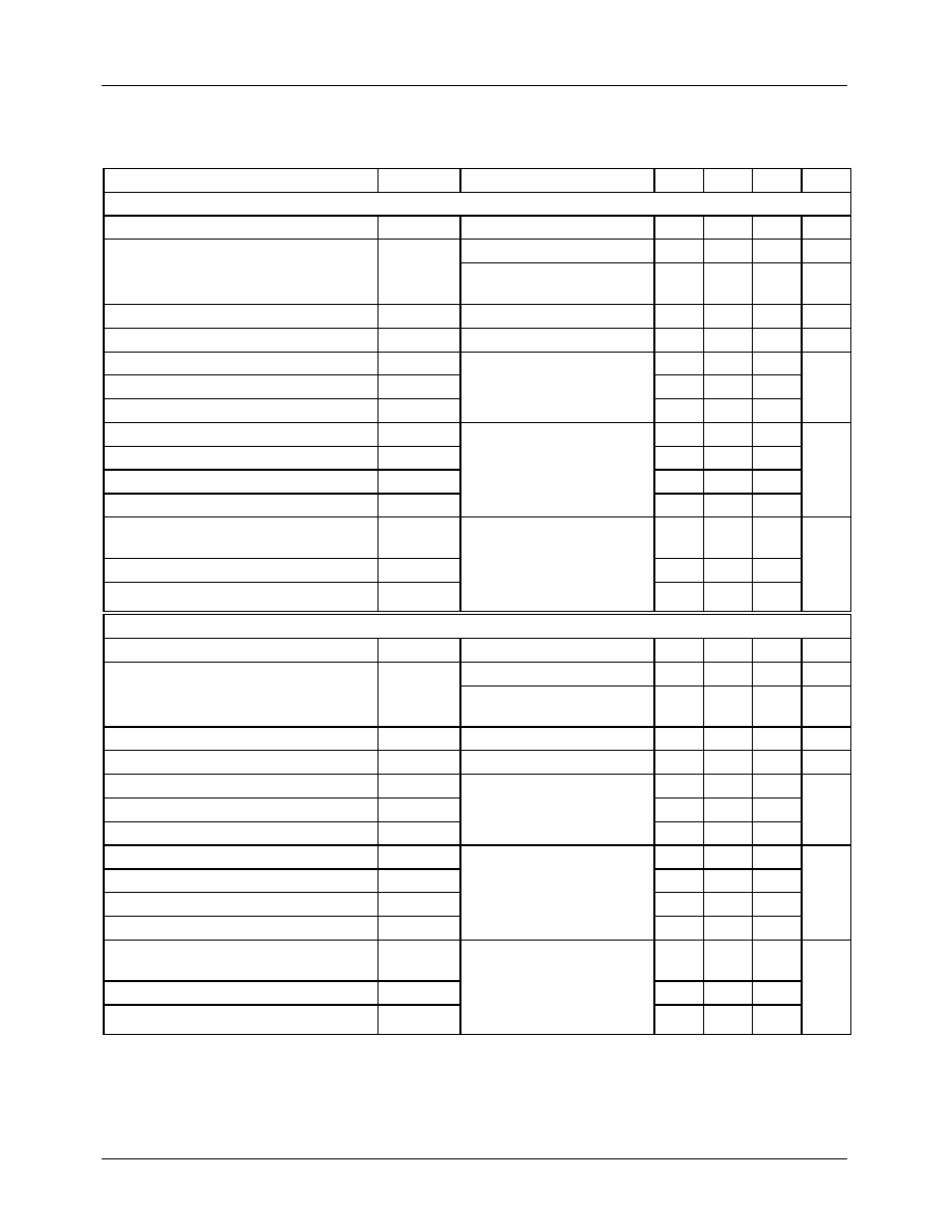
Absolute Maximum Ratings
(Ta=25
∞
C, unless otherwise specified)
Note:
1.
Repetitive rating: Pulse width limited by maximum junction temperature
2.
L
=
51mH, starting Tj
=
25
∞
C
3.
L
=
13
µ
H, starting Tj
=
25
∞
C
Characteristic
Symbol
Value
Unit
KA5H0365R, KA5M0365R, KA5L0365R
Maximum Drain Voltage
V
D,MAX
650
V
Drain-Gate Voltage (R
GS
=1M
)
V
DGR
650
V
Gate-Source (GND) Voltage
V
GS
±
30
V
Drain Current Pulsed
(1)
I
DM
12.0
A
DC
Continuous Drain Current (T
C
=25
∞
C)
I
D
3.0
A
DC
Continuous Drain Current (T
C
=100
∞
C)
I
D
2.4
A
DC
Single Pulsed Avalanche Energy
(2)
E
AS
358
mJ
Maximum Supply Voltage
V
CC,MAX
30
V
Analog Input Voltage Range
V
FB
-0.3 to V
SD
V
Total Power Dissipation
P
D
75
W
Derating
0.6
W/
∞
C
Operating Junction Temperature.
T
J
+160
∞
C
Operating Ambient Temperature.
T
A
-25 to +85
∞
C
Storage Temperature Range.
T
STG
-55 to +150
∞
C
KA5H0380R, KA5M0380R, KA5L0380R
Maximum Drain Voltage
V
D,MAX
800
V
Drain-Gate Voltage (R
GS
=1M
)
V
DGR
800
V
Gate-Source (GND) Voltage
V
GS
±
30
V
Drain Current Pulsed
(1)
I
DM
12.0
A
DC
Continuous Drain Current (T
C
=25
∞
C)
I
D
3.0
A
DC
Continuous Drain Current (T
C
=100
∞
C)
I
D
2.1
A
DC
Single Pulsed Avalanche Energy
(2)
E
AS
95
mJ
Maximum Supply Voltage
V
CC,MAX
30
V
Analog Input Voltage Range
V
FB
-0.3 to V
SD
V
Total Power Dissipation
P
D
75
W
Derating
0.6
W/
∞
C
Operating Junction Temperature.
T
J
+160
∞
C
Operating Ambient Temperature.
T
A
-25 to +85
∞
C
Storage Temperature Range.
T
STG
-55 to +150
∞
C

KA5X03XX-SERIES
3
Absolute Maximum Ratings
(Ta=25
∞
C, unless otherwise specified)
Note:
1.
Repetitive rating: Pulse width limited by maximum junction temperature
2.
L
=
51mH, starting Tj
=
25
∞
C
3.
L
=
13
µ
H, starting Tj
=
25
∞
C
Characteristic
Symbol
Value
Unit
KA5M0365RN, KA5L0365RN
Maximum Drain Voltage
V
D,MAX
650
V
Drain-Gate Voltage (R
GS
=1M
)
V
DGR
650
V
Gate-Source (GND) Voltage
V
GS
±
30
V
Drain Current Pulsed
(1)
I
DM
12.0
A
DC
Continuous Drain Current (Ta=25
∞
C)
I
D
0.42
A
DC
Continuous Drain Current (Ta=100
∞
C)
I
D
0.28
A
DC
Single Pulsed Avalanche Energy
(2)
E
AS
127
mJ
Maximum Supply Voltage
V
CC,MAX
30
V
Analog Input Voltage Range
V
FB
-0.3 to V
SD
V
Total Power Dissipation
P
D
1.56
W
Derating
0.0125
W/
∞
C
Operating Junction Temperature.
T
J
+160
∞
C
Operating Ambient Temperature.
T
A
-25 to +85
∞
C
Storage Temperature Range.
T
STG
-55 to +150
∞
C
KA5X03XX-SERIES
4
Electrical Characteristics (SenseFET Part)
(Ta = 25
∞
C unless otherwise specified)
Note:
1.
Pulse test: Pulse width
300
µ
S, duty
2%
2.
Parameter
Symbol
Condition
Min.
Typ.
Max.
Unit
KA5H0365R, KA5M0365R, KA5L0365R
Drain-Source Breakdown Voltage
BV
DSS
V
GS
=0V, I
D
=50
µ
A
650
-
-
V
Zero Gate Voltage Drain Current
I
DSS
V
DS
=Max. Rating, V
GS
=0V
-
-
50
µ
A
V
DS
=0.8Max. Rating,
V
GS
=0V, T
C
=125
∞
C
-
-
200
µ
A
Static Drain-Source on Resistance
(Note)
R
DS(ON)
V
GS
=10V, I
D
=0.5A
-
3.6
4.5
Forward Transconductance
(Note)
gfs
V
DS
=50V, I
D
=0.5A
2.0
-
-
S
Input Capacitance
Ciss
V
GS
=0V, V
DS
=25V,
f=1MHz
-
720
-
pF
Output Capacitance
Coss
-
40
-
Reverse Transfer Capacitance
Crss
-
40
-
Turn On Delay Time
td(on)
V
DD
=0.5BV
DSS
, I
D
=1.0A
(MOSFET switching
time is essentially
independent of
operating temperature)
-
150
-
nS
Rise Time
tr
-
100
-
Turn Off Delay Time
td(off)
-
150
-
Fall Time
tf
-
42
-
Total Gate Charge
(Gate-Source+Gate-Drain)
Qg
V
GS
=10V, I
D
=1.0A,
V
DS
=0.5BV
DSS
(MOSFET
switching time is essentially
independent of
operating temperature)
-
-
34
nC
Gate-Source Charge
Qgs
-
7.3
-
Gate-Drain (Miller) Charge
Qgd
-
13.3
-
KA5H0380R, KA5M0380R, KA5L0380R
Drain-Source Breakdown Voltage
BV
DSS
V
GS
=0V, I
D
=50
µ
A
800
-
-
V
Zero Gate Voltage Drain Current
I
DSS
V
DS
=Max. Rating, V
GS
=0V
-
-
250
µ
A
V
DS
=0.8Max. Rating,
V
GS
=0V, T
C
=125
∞
C
-
-
1000
µ
A
Static Drain-Source on Resistance
(Note)
R
DS(ON)
V
GS
=10V, I
D
=0.5A
-
4.0
5.0
Forward Transconductance
(Note)
gfs
V
DS
=50V, I
D
=0.5A
1.5
2.5
-
S
Input Capacitance
Ciss
V
GS
=0V, V
DS
=25V,
f=1MHz
-
779
-
pF
Output Capacitance
Coss
-
75.6
-
Reverse Transfer Capacitance
Crss
-
24.9
-
Turn On Delay Time
td(on)
V
DD
=0.5BV
DSS
, I
D
=1.0A
(MOSFET switching
time is essentially
independent of
operating temperature)
-
40
-
nS
Rise Time
tr
-
95
-
Turn Off Delay Time
td(off)
-
150
-
Fall Time
tf
-
60
-
Total Gate Charge
(Gate-Source+Gate-Drain)
Qg
V
GS
=10V, I
D
=1.0A,
V
DS
=0.5BV
DSS
(MOSFET
switching time is
essentially independent of
operating temperature)
-
-
34
nC
Gate-Source Charge
Qgs
-
7.2
-
Gate-Drain (Miller) Charge
Qgd
-
12.1
-
S
1
R
----
=

KA5X03XX-SERIES
5
Electrical Characteristics (SenseFET Part)
(Ta = 25
∞
C unless otherwise specified)
Note:
1.
Pulse test: Pulse width
300
µ
S, duty
2%
2.
Parameter
Symbol
Condition
Min.
Typ.
Max.
Unit
KA5M0365RN, KA5L0365RN
Drain-Source Breakdown Voltage
BV
DSS
V
GS
=0V, I
D
=50
µ
A
650
-
-
V
Zero Gate Voltage Drain Current
I
DSS
V
DS
=Max. Rating, V
GS
=0V
-
-
50
µ
A
V
DS
=0.8Max. Rating,
V
GS
=0V, T
C
=125
∞
C
-
-
200
µ
A
Static Drain-Source on Resistance
(Note)
R
DS(ON)
V
GS
=10V, I
D
=0.5A
-
3.6
4.5
Forward Transconductance
(Note)
gfs
V
DS
=50V, I
D
=0.5A
2.0
-
-
S
Input Capacitance
Ciss
V
GS
=0V, V
DS
=25V,
f=1MHz
-
314.9
-
pF
Output Capacitance
Coss
-
47
-
Reverse Transfer Capacitance
Crss
-
9
-
Turn On Delay Time
td(on)
V
DD
=0.5BV
DSS
, I
D
=1.0A
(MOSFET switching
time is essentially
independent of
operating temperature)
-
11.2
-
nS
Rise Time
tr
-
34
-
Turn Off Delay Time
td(off)
-
28.2
-
Fall Time
tf
-
32
-
Total Gate Charge
(Gate-Source+Gate-Drain)
Qg
V
GS
=10V, I
D
=1.0A,
V
DS
=0.5BV
DSS
(MOSFET
switching time is
essentially independent of
operating temperature)
11.93
nC
Gate-Source Charge
Qgs
-
1.95
-
Gate-Drain (Miller) Charge
Qgd
6.85
S
1
R
----
=

KA5X03XX-SERIES
6
Electrical Characteristics (Control Part)
(Continued)
(Ta = 25
∞
C unless otherwise specified)
Note:
1. These parameters, although guaranteed, are not 100% tested in production
2. These parameters, although guaranteed, are tested in EDS(water test) process
Characteristic
Symbol
Test condition
Min.
Typ.
Max.
Unit
UVLO SECTION
Start Threshold Voltage
V
START
V
FB
=GND
14
15
16
V
Stop Threshold Voltage
V
STOP
V
FB
=GND
8.4
9
9.6
V
OSCILLATOR SECTION
Initial Accuracy
F
OSC
KA5H0365R
KA5H0380R
90
100
110
kHz
Initial Accuracy
F
OSC
KA5M0365R
KA5M0365RN
KA5M0380R
61
67
73
kHz
Initial Accuracy
F
OSC
KA5L0365R
KA5L0365RN
KA5L0380R
45
50
55
kHz
Frequency Change With Temperature
(2)
-
-25
∞
C
Ta
+85
∞
C
-
±
5
±
10
%
Maximum Duty Cycle
Dmax
KA5H0365R
KA5H0380R
62
67
72
%
Maximum Duty Cycle
Dmax
KA5M0365R
KA5M0365RN
KA5M0380R
KA5L0365R
KA5L0365RN
KA5L0380R
72
77
82
%
FEEDBACK SECTION
Feedback Source Current
I
FB
Ta=25
∞
C, 0V<Vfb<3V
0.7
0.9
1.1
mA
Shutdown Feedback Voltage
V
SD
Vfb>6.5V
6.9
7.5
8.1
V
Shutdown Delay Current
Idelay
Ta=25
∞
C, 5V
Vfb
V
SD
4
5
6
µ
A
REFERENCE SECTION
Output Voltage
(1)
Vref
Ta=25
∞
C
4.80
5.00
5.20
V
Temperature Stability
(1)(2)
Vref/
T
-25
∞
C
Ta
+85
∞
C
-
0.3
0.6
mV/
∞
C
CURRENT LIMIT(SELF-PROTECTION)SECTION
Peak Current Limit
I
OVER
Max. inductor current
1.89
2.15
2.41
A
PROTECTION SECTION
Over Voltage Protection
V
OVP
V
CC
>24V
25
27
29
V
Thermal Shutdown Temperature (Tj)
(1)
T
SD
-
140
160
-
∞
C
TOTAL STANDBY CURRENT SECTION
Start-up Current
I
START
V
CC
=14V
-
100
170
µ
A
Operating Supply Current
(Control Part Only)
I
OP
V
CC
<28
-
7
12
mA

KA5X03XX-SERIES
7
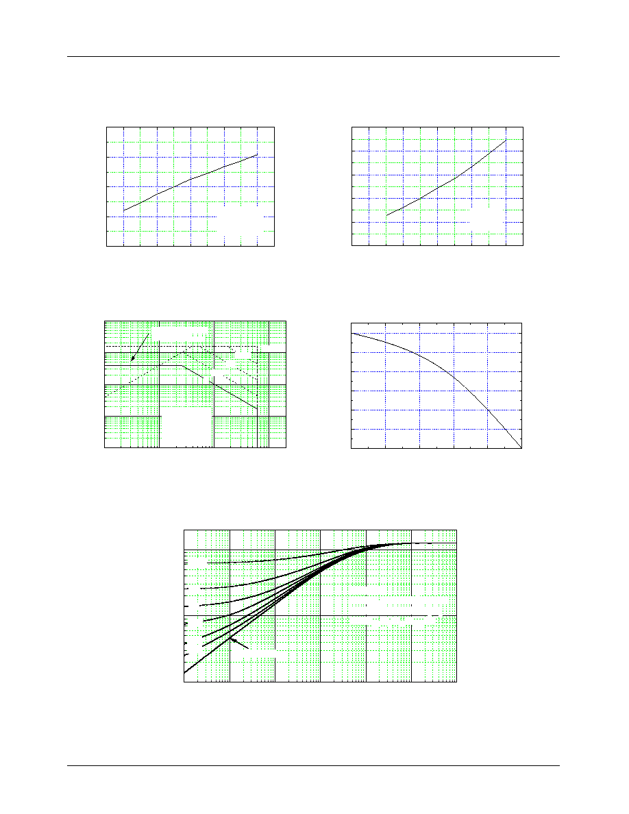
Typical Performance Characteristics(SenseFET part)
(KA5H0365R, KA5M0365R, KA5L0365R)
1
10
0.1
1
10
@Notes:
1. 300
µ
s Pulse Test
2. T
C
= 25
o
C
V
GS
Top : 15V
10V
8.0V
7.0V
6.0V
5.5V
5.0V
Bottom:4.5V
I
D
,
D
r
a
i
n
C
u
rr
ent
[
A
]
V
DS
, Drain-Source Voltage [V]
2
4
6
8
10
0.1
1
10
@Notes:
1. V
DS
= 30V
2. 300
µ
s Pulse Test
-25
o
C
25
o
C
150
o
C
I
D
,
D
r
a
i
n C
u
r
r
ent
[
A
]
V
GS
, Gate-Source Voltage [V]
0
1
2
3
4
5
0
1
2
3
4
5
6
7
@ Note : Tj=25
Vgs=10V
Vgs=20V
R
D
S
(
on)
, [
]
D
r
a
i
n-
S
our
c
e
O
n
-
R
es
i
s
t
anc
e
I
D
,Drain Current [A]
0.4
0.6
0.8
1.0
1.2
0.01
0.1
1
@Notes :
1. VGS = 0 V
2. 300
µ
s Pulse Test
25
o
C
150
o
C
I
DR
, R
e
v
e
r
s
e
D
r
ai
n
C
u
r
r
en
t
[A
]
V
SD
, Source-Drain Voltage [V]
10
0
10
1
0
100
200
300
400
500
600
700
C
rss
C
oss
C
iss
C
iss
= C
gs
+ C
gd
(C
ds
= shorted)
C
oss
= C
ds
+ C
gd
C
rss
= C
gd
C
a
paci
t
an
c
e
[
p
F
]
V
DS
, Drain-Source Voltage [V]
0
5
10
15
20
25
0
2
4
6
8
10
V
DS
=520V
V
DS
=320V
V
DS
=130V
@ Note : I
D
=3.0A
V
GS
,
G
at
e-
S
our
c
e
V
o
l
t
a
ge[
V
]
Q
G
,Total Gate Charge [nC]
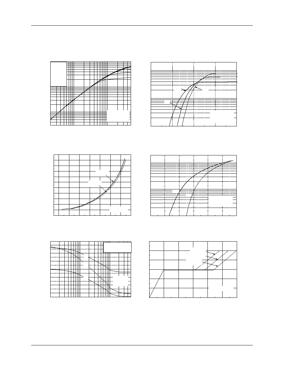
Figure 1. Output Characteristics
Figure 2. Transfer Characteristics
Figure 3. On-Resistance vs. Drain Current
Figure 4. Source-Drain Diode Forward Voltage
Figure 5. Capacitance vs. Drain-Source Voltage
Figure 6. Gate Charge vs. Gate-Source Voltage
KA5X03XX-SERIES
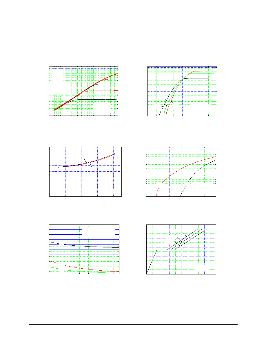
8
Typical Performance Characteristics
(Continued)
-50
0
50
100
150
0.8
0.9
1.0
1.1
1.2
@ Notes :
1. V
GS
= 0V
2. I
D
= 250
µ
A
T
J
, Junction Temperature [
o
C]
BV
DS
S
,
(
N
or
mal
i
z
ed)
D
r
a
i
n-
Sour
c
e
B
r
eak
d
o
w
n
V
o
l
t
a
g
e
-50
0
50
100
150
0.0
0.5
1.0
1.5
2.0
2.5
@ Notes:
1. V
GS
= 10V
2. I
D
= 1.5 A
T
J
, Junction Temperature [
o
C]
R
DS
(
o
n
)
,
(
N
or
m
a
l
i
z
e
d)
D
r
ai
n-
S
our
c
e
O
n
-
R
es
i
s
t
a
nc
e
10
0
10
1
10
2
10
3
10
-2
10
-1
10
0
10
1
10
2
10
µ
s
DC
100
µ
s
1 ms
10 ms
@ Notes :
1. T
C
= 25
o
C
2. T
J
= 150
o
C
3. Single Pulse
Operation in This Area
is Limited by R
DS(on)
I
D
,
Drain
Curr
ent
[A]
V
DS
, Drain-Source Voltage [V]
25
50
75
100
125
150
0.0
0.5
1.0
1.5
2.0
2.5
3.0
I
D
,
D
r
a
i
n C
u
r
r
ent [
A
]
T
C
, Case Temperature [
o
C]
10
-5
10
-4
10
-3
10
-2
10
-1
10
0
10
1
10
-2
10
-1
10
0
single pulse
0.2
0.1
0.01
0.02
0.05
D=0.5
@ Notes :
1. Z
JC
(t)=1.25
o
C/W Max.
2. Duty Factor, D=t
1
/t
2
3. T
JM
-T
C
=P
DM
*Z
JC
(t)
Z
JC
(t) ,
Therma
l Respon
se
t
1
, Square Wave Pulse Duration [sec]
Figure 7. Breakdown Voltage vs. Temperature
Figure 8. On-Resistance vs. Temperature
Figure 9. Max. Safe Operating Area
Figure 10. Max. Drain Current vs. Case Temperature
Figure 11. Thermal Response
KA5X03XX-SERIES
9
Typical Performance Characteristics
(Continued)
(KA5H0380R, KA5M0380R, KA5L0380R)
10
0
10
1
10
-1
10
0
10
1
@Notes:
1. 300
µ
s Pulse Test
2. T
C
= 25
o
C
V
GS
Top : 15V
10V
8.0V
7.0V
6.0V
5.5V
5.0V
Bottom:4.5V
I
D
, D
r
ai
n
C
u
r
r
e
n
t
[A
]
V
DS
, Drain-Source Voltage [V]
2
4
6
8
10
10
-1
10
0
10
1
@ Notes:
1. V
DS
= 30 V
2. 300
µ
s Pulse Test
-25
o
C
25
o
C
150
o
C
I
D
,
D
r
ai
n C
u
rr
ent
[
A
]
V
GS
, Gate-Source Voltage [V]
0.4
0.6
0.8
1.0
0.1
1
10
@ Notes:
1. V
GS
= 0V
2. 300
µ
s Pulse Test
25
o
C
150
o
C
I
DR
,
R
e
v
e
rs
e D
r
ai
n C
u
rrent
[
A
]
V
SD
, Source-Drain Voltage [V]
10
0
10
1
0
100
200
300
400
500
600
700
800
900
1000
C
rss
C
oss
C
iss
C
iss
= C
gs
+ C
gd
(C
ds
= shorted)
C
oss
= C
ds
+ C
gd
C
rss
= C
gd
Ca
pa
ci
ta
n
c
e [p
F
]
V
DS
, Drain-Source Voltage [V]
0
5
10
15
20
25
30
0
2
4
6
8
10
@ Note : I
D
=3.0A
V
DS
=640V
V
DS
=400V
V
DS
=160V
V
GS
,
G
a
t
e-S
ourc
e
V
o
l
t
age
[
V
]
Q
G
,Total Gate Charge [nC]
0
1
2
3
4
0
1
2
3
4
5
6
7
8
Vgs=10V
Vgs=20V
@ Note : Tj=25
Fig3. On-Resistance vs. Drain Current
R
D
S
(
on)
,
[
]
D
r
a
i
n-
S
o
u
r
c
e
O
n
-
R
es
i
s
t
a
nc
e
I
D
,Drain Current
Figure 1. Output Characteristics
Figure 2. Thansfer Characteristics
Figure 3. On-Resistance vs. Drain Current
Figure 4. Source-Drain Diode Forward Voltage
Figure 5. Capacitance vs. Drain-Source Voltage
Figure 6. Gate Charge vs. Gate-Source Voltage

KA5X03XX-SERIES
10
Typical Performance Characteristics
(Continued)
(KA5H0380R, KA5M0380R, KA5L0380R)
10
- 5
10
- 4
10
- 3
10
- 2
10
- 1
10
0
10
1
10
- 2
10
- 1
10
0
single pulse
0.2
0.1
0.01
0.02
0.05
D=0.5
@ Notes :
1. Z
J C
(t)=1.25
o
C/W Max.
2. Duty Factor, D=t
1
/t
2
3. T
J M
-T
C
=P
D M
*Z
J C
(t)
Z
JC
(t
) ,
T
her
mal
Res
pon
se
t
1
, Square Wave Pulse Duration [sec]
-50
0
50
100
150
0.8
0.9
1.0
1.1
1.2
@ Notes :
1. V
GS
= 0V
2. I
D
= 250
µ
A
T
J
, Junction Temperature [
o
C]
BV
DS
S
,
(
N
o
r
m
a
liz
e
d
)
D
r
ai
n
-
S
our
c
e
B
r
eak
dow
n
V
o
l
t
ag
e
-50
0
50
100
150
0.0
0.5
1.0
1.5
2.0
2.5
R
D
S
(
on)
,
(
N
or
m
a
l
i
z
ed)
D
r
ai
n-
S
our
c
e
O
n
-
R
es
i
s
t
anc
e
T
J
, Junction Temperature [
o
C]
@ Notes:
1. V
GS
= 10V
2. I
D
= 1.5 A
10
1
10
2
10
3
10
-2
10
-1
10
0
10
1
10
2
100
µ
s
DC
10
µ
s
1 ms
10 ms
@ Notes :
1. T
C
= 25
o
C
2. T
J
= 150
o
C
3. Single Pulse
Operation in This Area
is Limited by R
DS(on)
I
D
, Drai
n Current [
A
]
V
DS
, Drain-Source Voltage [V]
40
60
80
100
120
140
0.0
0.5
1.0
1.5
2.0
2.5
3.0
3.5
I
D
,
D
r
ai
n C
u
r
r
ent
[
A
]
T
C
, Case Temperature [
o
C]
Figure 7. Breakdown Voltage vs. Temperature
Figure 8. On-Resistance vs. Temperature
Figure 9. Max. Safe Operating Area
Figure 10. Max. Drain Current vs. Case Temperature
Figure 11. Thermal Response
KA5X03XX-SERIES
11
Typical Performance Characteristics(SenseFET part)
(Continued)
(KA5M0365RN, KA5L0365RN)
10
0
10
1
10
-1
10
0
10
1
V
GS
Top : 15.0 V
10.0 V
8.0 V
7.0 V
6.5 V
6.0 V
Bottom : 5.5 V
Note :
1. 250
s Pulse Test
2. T
C
= 25
I
D
,
D
r
ai
n
C
u
r
r
e
nt
[
A
]
V
DS
, Drain-Source Voltage [V]
2
4
6
8
10
10
-1
10
0
10
1
Note
1. V
DS
= 50V
2. 250
s Pulse Test
-55
150
25
I
D
,
D
r
ai
n C
u
r
r
ent
[
A
]
V
GS
, Gate-Source Voltage [V]
0
1
2
3
4
5
6
7
2.5
3.0
3.5
4.0
4.5
5.0
5.5
6.0
6.5
7.0
7.5
8.0
V
GS
= 20V
V
GS
= 10V
Note : T
J
= 25
R
DS(
O
N)
[
],
D
r
ai
n
-
S
o
ur
c
e
O
n
-
R
es
i
s
t
a
nc
e
I
D
, Drain Current [A]
0.2
0.4
0.6
0.8
1.0
1.2
1.4
10
-1
10
0
10
1
25
150
Note :
1. V
GS
= 0V
2. 250
s Pulse Test
I
DR
, R
e
v
e
r
s
e
D
r
a
i
n
C
u
r
r
e
n
t
[
A
]
V
SD
, Source-Drain Voltage [V]
10
-1
10
0
10
1
100
200
300
400
500
600
700
C
iss
= C
gs
+ C
gd
(C
ds
= shorted)
C
oss
= C
ds
+ C
gd
C
rss
= C
gd
Note ;
1. V
GS
= 0 V
2. f = 1 MHz
C
rss
C
oss
C
iss
C
a
p
a
citanc
es [
p
F]
V
DS
, Drain-Source Voltage [V]
0
2
4
6
8
10
12
0
2
4
6
8
10
12
V
DS
= 325V
V
DS
= 130V
V
DS
= 520V
Note : I
D
= 3.0 A
V
GS
, G
a
te-Source Vol
t
ag
e [V]
Q
G
, Total Gate Charge [nC]
Figure 1. Output Characteristics
Figure 2. Transfer Characteristics
Figure 3. On-Resistance vs. Drain Current
Figure 4. Source-Drain Diode Forward Voltage
Figure 5. Capacitance vs. Drain-Source Voltage
Figure 6. Gate Charge vs. Gate-Source Voltage

KA5X03XX-SERIES
12
Typical Performance Characteristics
(Continued)
( KA5M0365RN, KA5L0365RN)
-50
0
50
100
150
0.90
0.95
1.00
1.05
1.10
1.15
Note :
1. V
GS
= 0 V
2. I
D
= 250
A
BV
DS
S
,
(
N
or
m
a
l
i
z
ed)
D
r
ai
n-
So
ur
ce Br
eakdow
n
V
o
l
t
age
T
J
, Junction Temperature [
o
C]
-50
0
50
100
150
0.5
1.0
1.5
2.0
2.5
Note :
1. V
GS
= 10 V
2. I
D
= 1.5 A
R
DS
(O
N
)
,
(
N
or
m
a
l
i
zed)
Dr
ai
n-
Sour
ce
On-
R
esi
s
t
a
nce
T
J
, Junction Temperature [
o
C]
Figure 7. Breakdown Voltage vs. Temperature
Figure 8. On-Resistance vs. Temperature
Figure 9. Max. Safe Operating Area
Figure 10. Max. Drain Current vs. Case Temperature
Figure 11. Thermal Response
10
0
10
1
10
2
10
-3
10
-2
10
-1
10
0
10
1
DC
10 s
1 s
100 ms
10 ms
1 ms
100
µ
s
10
µ
s
Operation in This Area
is Limited by R
DS(on)
I
D
,
Dr
a
i
n
Cu
r
r
e
n
t
[
A
]
V
DS
, Drain-Source Voltage [V]
25
50
75
100
125
150
0.0
0.1
0.2
0.3
0.4
0.5
I
D
,
D
r
ai
n C
u
r
r
ent
[
A
]
T
C
, Case Temperature [? ]
1E-5
1E-4
1E-3
0.01
0.1
1
10
100
1000
0.1
1
10
0.05
0.02
0.01
single pulse
0.2
0.1
D=0.5
? Notes :
1. Z
? JC
(t) = 80 ? /W Max.
2. Duty Factor, D=t
1
/t
2
3. T
JM
- T
C
= P
DM
* Z
? JC
(t)
Z
?J
C
(
t
)
,
T
her
m
a
l
R
e
sp
onse
t
1
, Square Wave Pulse Duration [sec]
KA5X03XX-SERIES
13
Typical Performance Characteristics (Control Part)
(Continued)
(These characteristic graphs are normalized at Ta = 25
∞
C)
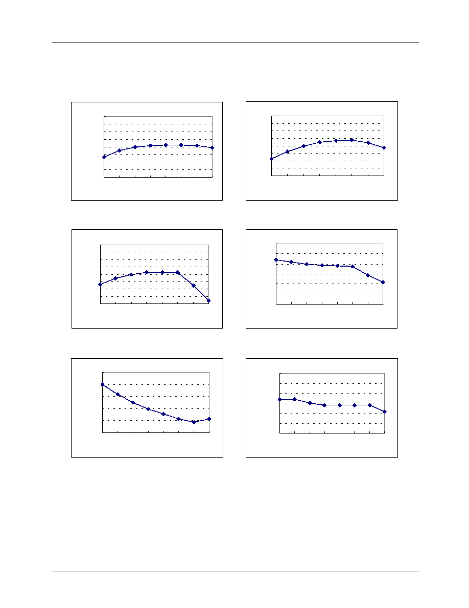
Fig.1 Operating Frequency
0.8
0.85
0.9
0.95
1
1.05
1.1
1.15
1.2
-25
0
25
50
75
100 125 150
Fosc
Fig.2 Feedback Source Current
0.8
0.85
0.9
0.95
1
1.05
1.1
1.15
1.2
-25
0
25
50
75
100 125 150
Ifb
Fig.3 Operating Current
0.8
0.85
0.9
0.95
1
1.05
1.1
1.15
1.2
-25
0
25
50
75
100 125 150
Iop
Fig.4 Max Inductor Current
0.8
0.85
0.9
0.95
1
1.05
1.1
-25
0
25
50
75
100 125 150
Ipeak
Fig.5 Start up Current
0.5
0.7
0.9
1.1
1.3
1.5
-25
0
25
50
75
100 125 150
Istart
Fig.6 Start Threshold Voltage
0.85
0.9
0.95
1
1.05
1.1
1.15
-25
0
25
50
75 100 125 150
Vstart
Figure 1. Operating Frequency
Figure 2. Feedback Source Current
Figure 3. Operating Supply Current
Figure 4. Peak Current Limit
Figure 5. Start up Current
Figure 6. Start Threshold Voltage
I
over
KA5X03XX-SERIES
14
Typical Performance Characteristics
(Continued)
(These characteristic graphs are normalized at Ta = 25
∞
C)
Fig.7 Stop Threshold Voltage
0.85
0.9
0.95
1
1.05
1.1
1.15
-25
0
25
50
75
100 125 150
Vstop
Fig.8 Maximum Duty Cycle
0.85
0.9
0.95
1
1.05
1.1
1.15
-25
0
25
50
75 100 125 150
Dmax
Fig.9 Vcc Zener Voltage
0.8
0.85
0.9
0.95
1
1.05
1.1
1.15
1.2
-25
0
25
50
75
100 125 150
Vz
Fig.10 Shutdown Feedback Voltage
0.85
0.9
0.95
1
1.05
1.1
1.15
-25
0
25
50
75
100 125 150
Vsd
Fig.11 Shutdown Delay Current
0.8
0.85
0.9
0.95
1
1.05
1.1
1.15
1.2
-25
0
25
50
75
100 125 150
Idelay
Fig.12 Over Voltage Protection
0.85
0.9
0.95
1
1.05
1.1
1.15
-25
0
25
50
75
100 125 150
Vovp
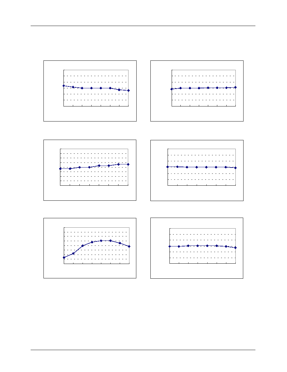
Figure 7. Stop Threshold Voltage
Figure 8. Maximum Duty Cycle
Figure 9. V
CC
Zener Voltage
Figure 10. Shutdown Feedback Voltage
Figure 11. Shutdown Delay Current
Figure 12. Over Voltage Protection
KA5X03XX-SERIES
15
Typical Performance Characteristics
(Continued)
(These characteristic graphs are normalized at Ta = 25
∞
C)
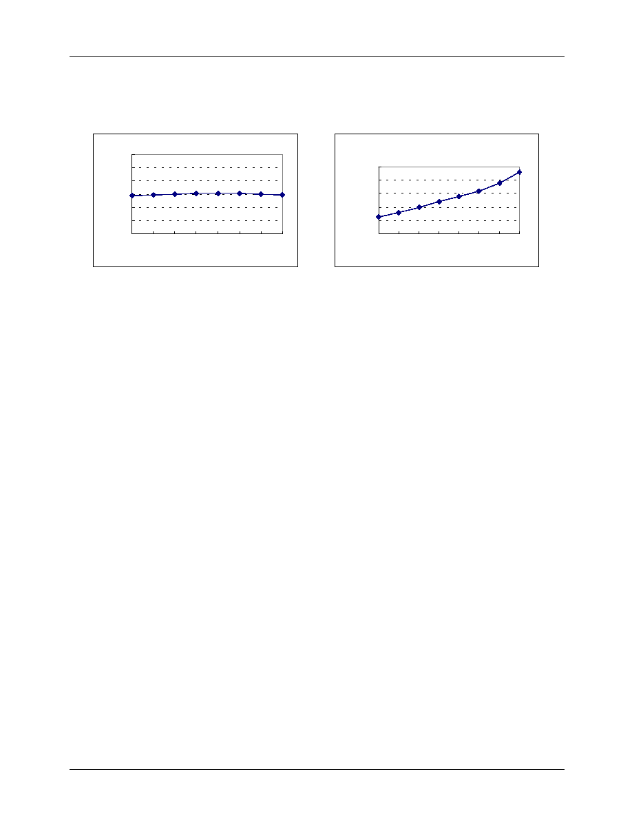
Figure13. Soft Start Voltage
Figure 14. Static Drain-Source on Resistance
Fig.13 Soft Start Voltage
0.85
0.9
0.95
1
1.05
1.1
1.15
-25
0
25
50
75
100 125 150
Vss
Fig.14 Drain Source Turn-on
Resistance
0
0.5
1
1.5
2
2.5
-25
0
25
50
75 100 125 150
Rdson
( )

KA5X03XX-SERIES
16
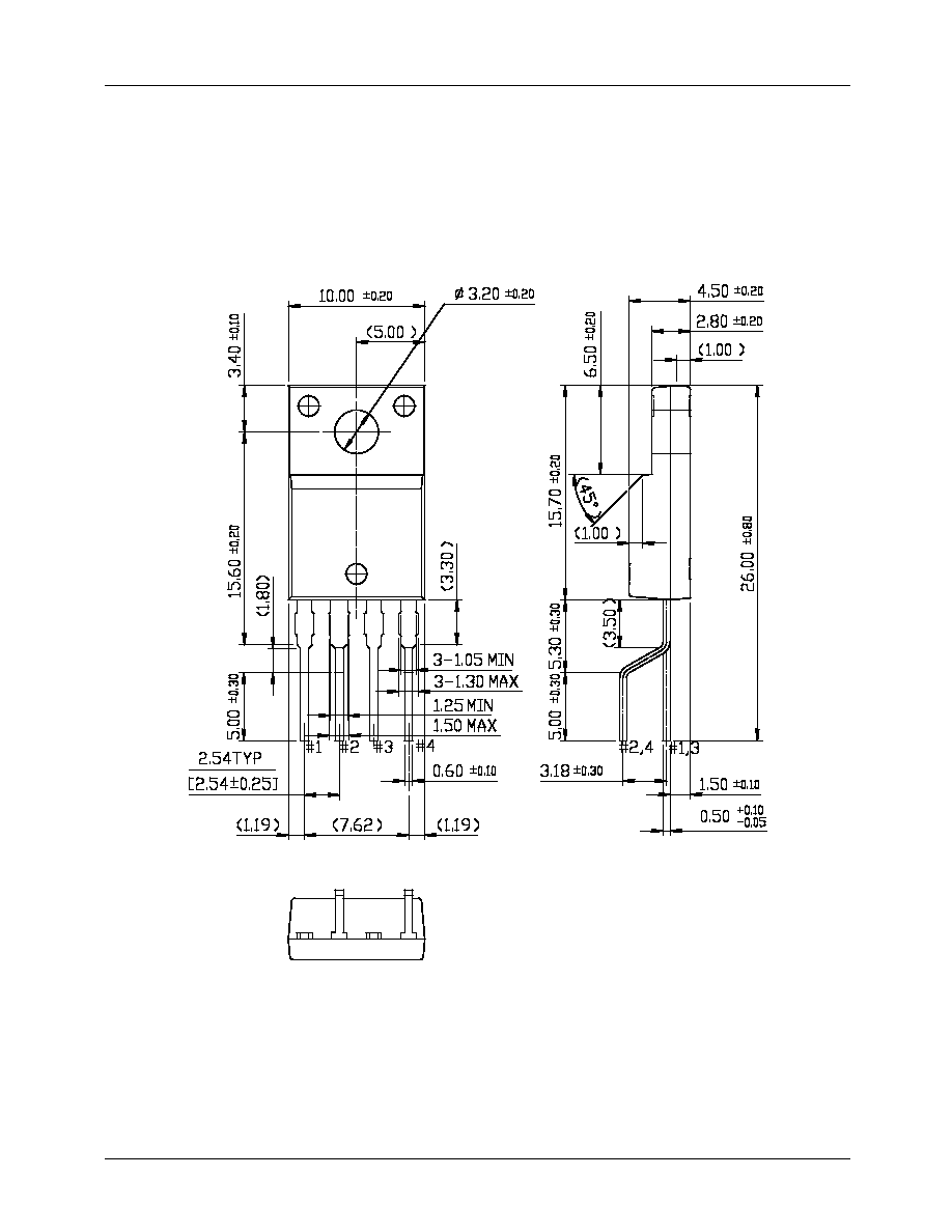
Package Dimensions
TO-220F-4L
KA5X03XX-SERIES
17
Package Dimensions
(Continued)
TO-220F-4L(Forming)
KA5X03XX-SERIES
18
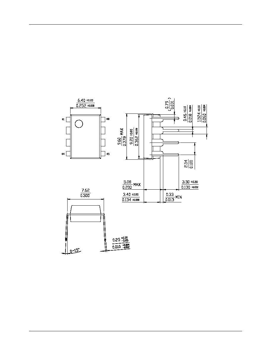
Package Dimensions
(Continued)
8-DIP
KA5X03XX-SERIES
19
Ordering Information
TU :Non Forming Type
YDTU : Forming type
Product Number
Package
Marking Code
BV
DSS
F
OSC
R
DS(on)
KA5H0365RTU
TO-220F-4L
5H0365R
650V
100kHz
3.6
KA5H0365RYDTU
TO-220F-4L(Forming)
KA5M0365RTU
TO-220F-4L
5M0365R
650V
67kHz
3.6
KA5M0365RYDTU
TO-220F-4L(Forming)
KA5L0365RTU
TO-220F-4L
5L0365R
650V
50kHz
3.6
KA5L0365RYDTU
TO-220F-4L(Forming)
KA5M0365RN
8-DIP
5M0365R
650V
67kHz
3.6
KA5L0365RN
8-DIP
5L0365R
650V
50kHz
3.6
Product Number
Package
Marking Code
BV
DSS
F
OSC
R
DS(on)
KA5H0380RTU
TO-220F-4L
5H0380R
800V
100kHz
4.6
KA5H0380RYDTU
TO-220F-4L(Forming)
KA5M0380RTU
TO-220F-4L
5M0380R
800V
67kHz
4.6
KA5M0380RYDTU
TO-220F-4L(Forming)
KA5L0380RTU
TO-220F-4L
5L0380R
800V
50kHz
4.6
KA5L0380RYDTU
TO-220F-4L(Forming)

KA5X03XX-SERIES
12/12/02 0.0m 001
Stock#DSxxxxxxxx
2002 Fairchild Semiconductor Corporation
LIFE SUPPORT POLICY
FAIRCHILD'S PRODUCTS ARE NOT AUTHORIZED FOR USE AS CRITICAL COMPONENTS IN LIFE SUPPORT DEVICES
OR SYSTEMS WITHOUT THE EXPRESS WRITTEN APPROVAL OF THE PRESIDENT OF FAIRCHILD SEMICONDUCTOR
CORPORATION. As used herein:
1. Life support devices or systems are devices or systems
which, (a) are intended for surgical implant into the body,
or (b) support or sustain life, and (c) whose failure to
perform when properly used in accordance with
instructions for use provided in the labeling, can be
reasonably expected to result in a significant injury of the
user.
2. A critical component in any component of a life support
device or system whose failure to perform can be
reasonably expected to cause the failure of the life support
device or system, or to affect its safety or effectiveness.
www.fairchildsemi.com
DISCLAIMER
FAIRCHILD SEMICONDUCTOR RESERVES THE RIGHT TO MAKE CHANGES WITHOUT FURTHER NOTICE TO ANY
PRODUCTS HEREIN TO IMPROVE RELIABILITY, FUNCTION OR DESIGN. FAIRCHILD DOES NOT ASSUME ANY
LIABILITY ARISING OUT OF THE APPLICATION OR USE OF ANY PRODUCT OR CIRCUIT DESCRIBED HEREIN; NEITHER
DOES IT CONVEY ANY LICENSE UNDER ITS PATENT RIGHTS, NOR THE RIGHTS OF OTHERS.