 | –≠–ª–µ–∫—Ç—Ä–æ–Ω–Ω—ã–π –∫–æ–º–ø–æ–Ω–µ–Ω—Ç: 6N139SV | –°–∫–∞—á–∞—Ç—å:  PDF PDF  ZIP ZIP |
©2005 Fairchild Semiconductor Corporation
1
www.fairchildsemi.com
July 2005
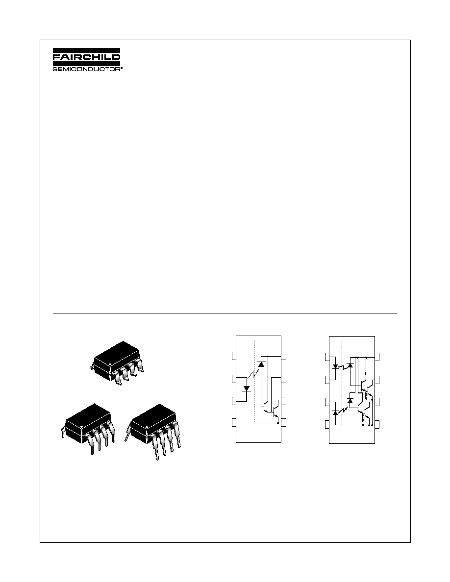
Single-Channel: 6N138, 6N139 Dual-Channel: HCPL-2730, HCPL-2731 Rev. 1.0.0
Single-Channel: 6N138, 6N139 Dual-Channel: HCPL-2730, HCPL-2731 Low Input Current High Gain Split Darlington Optocouplers
Single-Channel: 6N138, 6N139
Dual-Channel: HCPL-2730, HCPL-2731
Low Input Current High Gain Split
Darlington Optocouplers
Features
Low current - 0.5 mA
Superior CTR-2000%
Superior CMR-10 kV/µs
CTR guaranteed 0-70∞C
U.L. recognized (File # E90700)
VDE recognized (File # 120915) Ordering option
V, e.g., 6N138V
Dual Channel - HCPL-2730
HCPL-2731
Applications
Digital logic ground isolation
Telephone ring detector
EIA-RS-232C line receiver
High common mode noise line receiver
µP bus isolation
Current loop receiver
Description
The 6N138/9 and HCPL-2730/HCPL-2731 optocouplers consist
of an AlGaAs LED optically coupled to a high gain split darling-
ton photodetector.
The split darlington configuration separating the input photo-
diode and the first stage gain from the output transistor permits
lower output saturation voltage and higher speed operation than
possible with conventional darlington phototransistor optocou-
pler. In the dual channel devices, HCPL-2730/HCPL2731, an
integrated emitter - base resistor provides superior stability over
temperature.
The combination of a very low input current of 0.5 mA and a
high current transfer ratio of 2000% makes this family particu-
larly useful for input interface to MOS, CMOS, LSTTL and EIA
RS232C, while output compatibility is ensured to CMOS as well
as high fan-out TTL requirements. An internal noise shield pro-
vides exceptional common mode rejection of 10 kV/µs.
Package
Schematic
8
8
1
8
1
1
1
2
3
4
5
6
7
8
+
_
V
F
V
CC
V
B
V
O
GND
6N138 / 6N139
N/C
N/C
1
2
3
4
5
6
7
8
+
_
V
F1
V
CC
V
01
V
02
GND
HCPL-2730 / HCPL-2731
V
F2
_
+
2
www.fairchildsemi.com
Single-Channel: 6N138, 6N139 Dual-Channel: HCPL-2730, HCPL-2731 Rev. 1.0.0
Single-Channel: 6N138, 6N139 Dual-Channel: HCPL-2730, HCPL-2731 Low Input Current High Gain Split Darlington Optocouplers
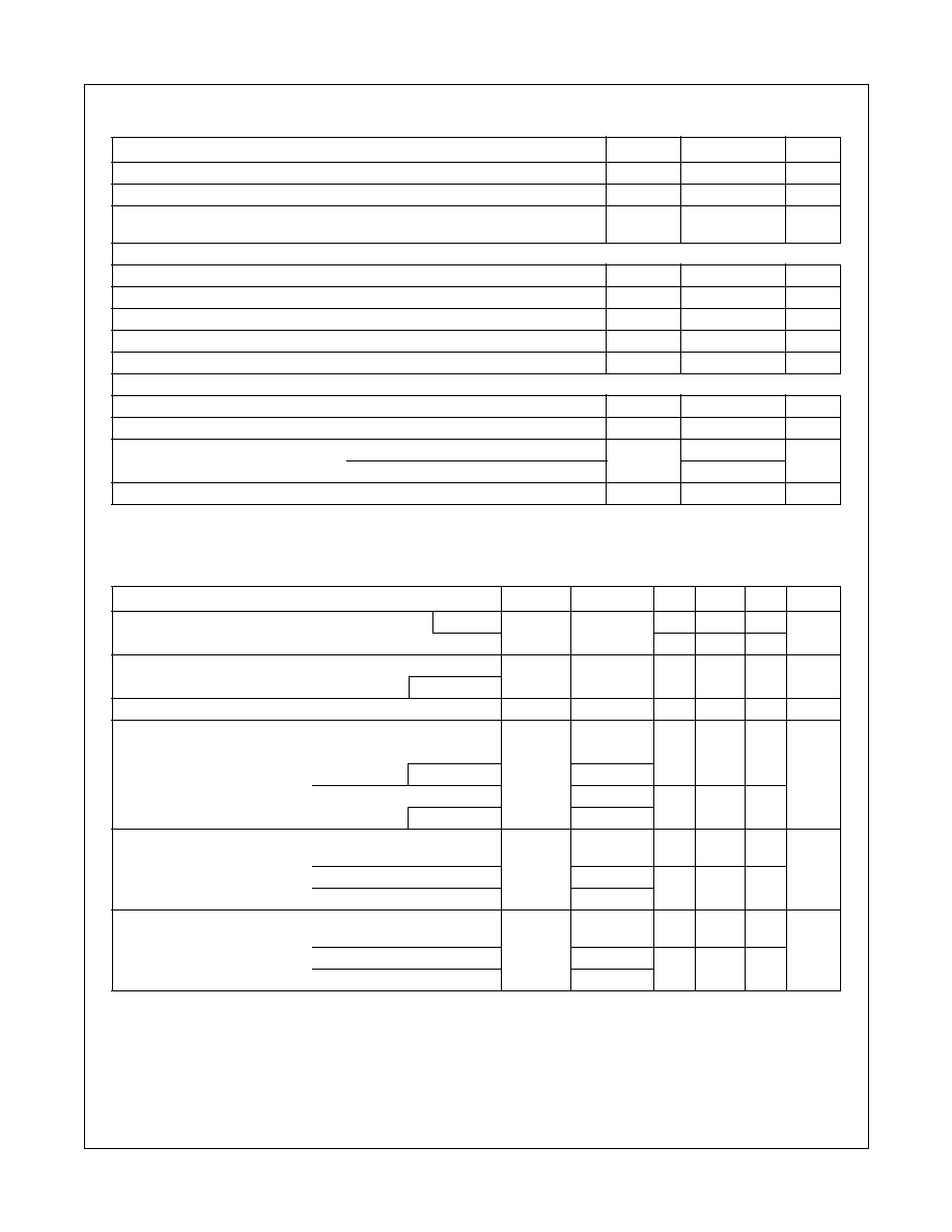
Absolute Maximum Ratings
(T
A
= 25∞C unless otherwise specified)
Electrical Characteristics
(T
A
= 0 to 70∞C Unless otherwise specified)
Individual Component Characteristics
** All Typicals at T
A
= 25∞C
Parameter
Symbol
Value
Units
Storage Temperature
T
STG
-55 to +125
∞C
Operating Temperature
T
OPR
-40 to +85
∞C
Lead Solder Temperature (Wave solder only. See recommended reflow profile graph for
SMD mounting)
T
SOL
260 for 10 sec
∞C
EMITTER
DC/Average Forward Input Current
Each Channel
I
F
(avg)
20
mA
Peak Forward Input Current (50% duty cycle, 1 ms P.W.)
Each Channel
I
F
(pk)
40
mA
Peak Transient Input Current - (
1 µs P.W., 300 pps)
I
F
(trans)
1.0
A
Reverse Input Voltage
Each Channel
V
R
5
V
Input Power Dissipation
Each Channel
P
D
35
mW
DETECTOR
Average Output Current
Each Channel
I
O
(avg)
60
mA
Emitter-Base Reverse Voltage
(6N138 and 6N139)
V
ER
0.5
V
Supply Voltage, Output Voltage
(6N138, HCPL-2730)
V
CC
, V
O
-0.5 to 7
V
(6N139, HCPL-2731)
-0.5 to 18
Output Power Dissipation
Each Channel
P
O
100
mW
Parameter
Test Conditions Symbol
Device
Min Typ** Max
Unit
EMITTER
T
A
=25∞C
V
F
All
1.30
1.7
V
Input Forward Voltage
Each channel (I
F
= 1.6 mA)
1.75
Input Reverse Breakdown Voltage
(T
A
= 25∞C, I
R
= 10 µA)
BV
R
All
5.0
20
V
Each Channel
Temperature coefficient of forward voltage (I
F
= 1.6 mA)
(
V
F
/
T
A
)
All
-1.8
mV/∞C
DETECTOR
Logic high output current
(I
F
= 0 mA, V
O
= V
CC
= 18 V)
I
OH
6N139
0.01
100
µA
Each Channel
HCPL-2731
(I
F
= 0 mA, V
O
= V
CC
= 7 V)
6N138
0.01
250
Each Channel
HCPL-2730
Logic low supply
(I
F
= 1.6 mA, V
O
= Open)
(V
CC
= 18 V)
I
CCL
6N138
6N139
0.4
1.5
mA
(I
F1
= I
F2
= 1.6 mA, V
CC
= 18 V)
HCPL-2731
1.3
3
(V
O1
- V
O2
= Open, V
CC
= 7 V
HCPL-2730
Logic high supply
(I
F
= 0 mA, V
O
= Open,
V
CC
= 18 V)
I
CCH
6N135
6N136
0.05
10
µA
(I
F1
= I
F2
= 0 mA, V
CC
= 18 V)
HCPL-2731
0.10
20
(V
O1
- V
O2
= Open, V
CC
= 7 V
HCPL-2730
3
www.fairchildsemi.com
Single-Channel: 6N138, 6N139 Dual-Channel: HCPL-2730, HCPL-2731 Rev. 1.0.0
Single-Channel: 6N138, 6N139 Dual-Channel: HCPL-2730, HCPL-2731 Low Input Current High Gain Split Darlington Optocouplers
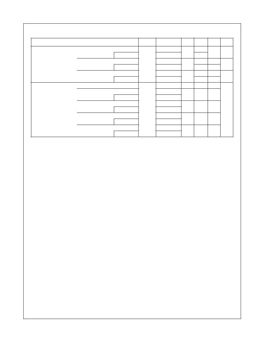
Transfer Characteristics
(T
A
= 0 to 70∞C Unless otherwise specified)
** All Typicals at T
A
= 25∞C
Parameter
Test Conditions Symbol
Device
Min
Typ**
Max
Unit
COUPLED
(I
F
= 0.5 mA, V
O
= 0.4 V, V
CC
= 4.5 V)
CTR
6N139
400
1100
%
Current transfer ratio
(Note 1, 2)
Each Channel
HCPL-2731
3500
(I
F
= 1.6 mA, V
O
= 0.4 V, V
CC
= 4.5 V)
6N139
500
1300
%
Each Channel
HCPL-2731
2500
(I
F
= 1.6 mA, V
O
= 0.4 V, V
CC
= 4.5 V)
6N138
300
1300
%
Each Channel
HCPL-2730
2500
Logic low output voltage
output voltage (Note 2)
(I
F
= 0.5 mA, I
O
= 2 mA, V
CC
= 4.5 V)
V
OL
6N139
0.08
0.4
V
(I
F
= 1.6 mA, I
O
= 8 mA, V
CC
= 4.5 V)
6N139
0.01
0.4
Each Channel
HCPL-2731
(I
F
= 0.5 mA, I
O
= 15 mA, V
CC
= 4.5 V)
6N139
0.13
0.4
Each Channel
HCPL-2731
(I
F
= 12 mA, I
O
= 24 mA, V
CC
= 4.5 V)
6N139
0.20
0.4
Each Channel
HCPL-2731
(I
F
= 1.6 mA, I
O
= 4.8 mA, V
CC
= 4.5 V)
6N138
0.10
0.4
Each Channel
HCPL-2730
4
www.fairchildsemi.com
Single-Channel: 6N138, 6N139 Dual-Channel: HCPL-2730, HCPL-2731 Rev. 1.0.0
Single-Channel: 6N138, 6N139 Dual-Channel: HCPL-2730, HCPL-2731 Low Input Current High Gain Split Darlington Optocouplers
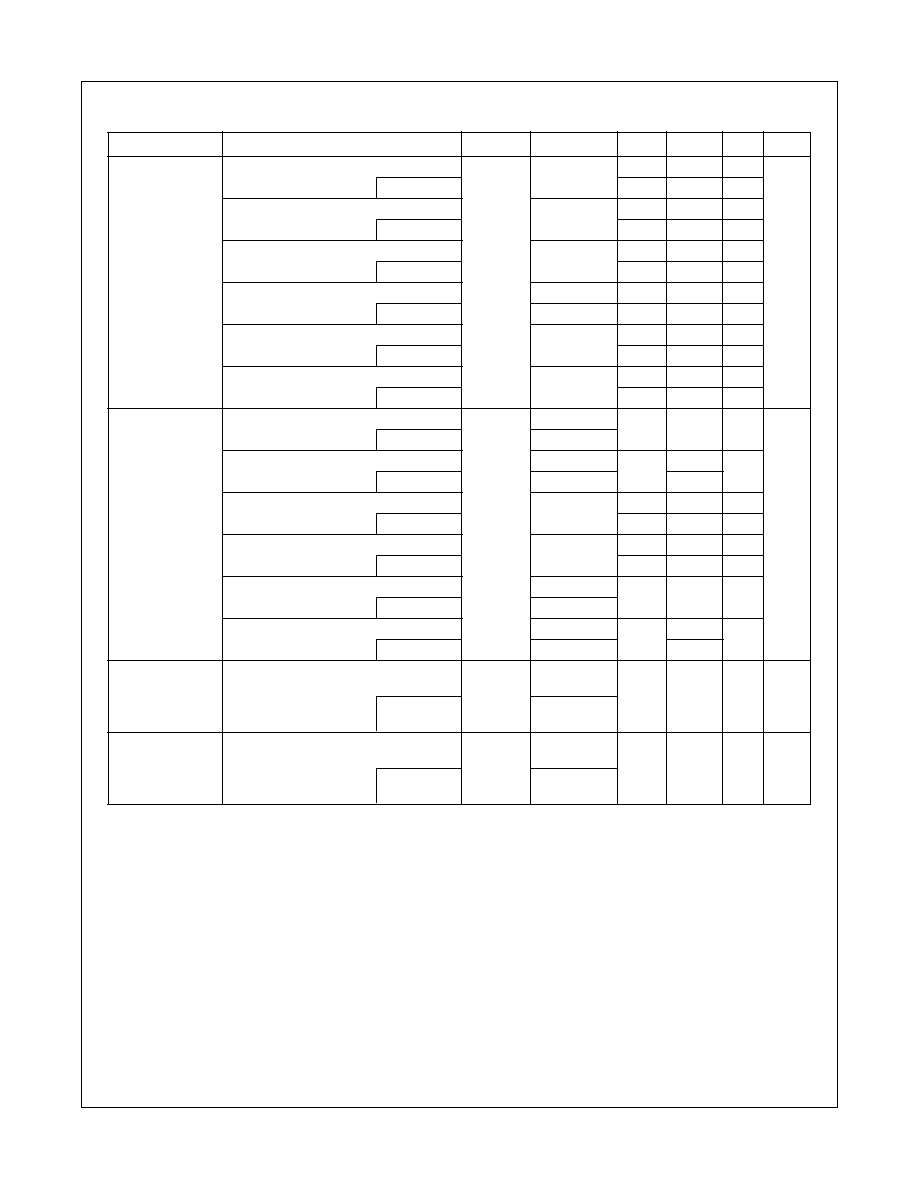
Switching Characteristics
(T
A
= 0 to 70∞C unless otherwise specified., V
CC
= 5 V)
** All Typicals at T
A
= 25∞C
Parameter
Test Conditions Symbol
Device
Min
Typ**
Max
Unit
Propagation delay
time to logic low
(Note 2) (Fig. 22)
(R
L
= 4.7 k
, I
F
= 0.5 mA)
T
PHL
6N139
30
µs
T
A
= 25∞C
4
25
(R
L
= 4.7 k
, I
F
= 0.5 mA)
HCPL-2731
120
Each Channel
T
A
= 25∞C
3
100
(R
L
= 270
, I
F
= 12 mA)
6N139
2
T
A
= 25∞C
0.2
1
(R
L
= 270
, I
F
= 12 mA)
HCPL-2730
3
Each Channel
T
A
= 25∞C
HCPL-2731
0.3
2
(R
L
= 2.2 k
, I
F
= 1.6 mA)
6N138
15
T
A
= 25∞C
1.5
10
(R
L
= 2.2 k
, I
F
= 1.6 mA)
HCPL-2731
HCPL-2730
25
Each Channel
T
A
= 25∞C
1
20
Propagation delay
time to logic high
(Note 2) (Fig. 22)
(R
L
= 4.7 k
, I
F
= 0.5 mA)
T
PLH
6N139
90
µs
Each Channel
HCPL-2731
(R
L
= 4.7 k
, I
F
= 0.5 mA) T
A
= 25∞C
6N139
12
60
Each Channel
HCPL-2731
22
(R
L
= 270
, I
F
= 12 mA)
6N139
10
T
A
= 25∞C
1.3
7
(R
L
= 270
, I
F
= 12 mA) Each Channel
HCPL-2730
HCPL-2731
15
T
A
= 25∞C
5
10
(R
L
= 2.2 k
, I
F
= 1.6 mA)
6N138
50
Each Channel
HCPL-2730/1
(R
L
= 2.2 k
, I
F
= 1.6 mA) T
A
= 25∞C
6N138
7
35
Each Channel
HCPL-2730/1
16
Common mode
transient immunity
at logic high
(I
F
= 0 mA, |V
CM
| = 10 V
P-P
)
T
A
= 25∞C, (R
L
= 2.2 k
) (Note 3) (Fig. 23)
|CM
H
|
6N138
6N139
1,000
10,000
V/µs
Each Channel
HCPL-2730
HCPL-2731
Common mode
transient immunity
at logic low
(I
F
= 1.6 mA, |V
CM
| = 10 V
P-P
, R
L
= 2.2 k
)
T
A
= 25∞C, (Note 3) (Fig. 23)
|CM
L
|
6N138
6N139
1,000
10,000
V/µs
Each Channel
HCPL-2730
HCPL-2731
5
www.fairchildsemi.com
Single-Channel: 6N138, 6N139 Dual-Channel: HCPL-2730, HCPL-2731 Rev. 1.0.0
Single-Channel: 6N138, 6N139 Dual-Channel: HCPL-2730, HCPL-2731 Low Input Current High Gain Split Darlington Optocouplers
Isolation Characteristics
(T
A
= 0 to 70∞C Unless otherwise specified)
** All Typicals at T
A
= 25∞C
Notes
1. Current Transfer Ratio is defined as a ratio of output collector current, I
O
, to the forward LED input current, I
F
, times 100%.
2. Pin 7 open. (6N138 and 6N139 only)
3. Common mode transient immunity in logic high level is the maximum tolerable (positive) dV
cm
/dt on the leading edge of the com-
mon mode pulse signal V
CM
, to assure that the output will remain in a logic high state (i.e., V
O
>2.0 V). Common mode transient
immunity in logic low level is the maximum tolerable (negative) dV
cm
/dt on the trailing edge of the common mode pulse signal,
V
CM
, to assure that the output will remain in a logic low state (i.e., V
O
<0.8 V).
4. Device is considered a two terminal device: Pins 1, 2, 3 and 4 are shorted together and Pins 5, 6, 7 and 8 are shorted together.
5. For dual channel devices, C
I-O
is measured by shorting pins 1 and 2 or pins 3 and 4 together and pins 5 through 8 shorted
together.
6. Measured between pins 1 and 2 shorted together, and pins 3 and 4 shorted together.
I
Characteristics
Test Conditions Symbol
Min
Typ**
Max
Unit
Input-output
insulation leakage current
(Relative humidity = 45%)
(T
A
= 25∞C, t = 5 s)
(V
I-O
= 3000 VDC)
(Note 8)
I
I-O
1.0
µA
Withstand insulation test voltage
(RH
50%, T
A
= 25∞C)
(Note 4) ( t = 1 min.)
V
ISO
2500
V
RMS
Resistance (input to output)
(Note 4) (V
I-O
= 500 VDC)
R
I-O
10
12
Capacitance (input to output)
(Note 4, 5) (f = 1 MHz)
C
I-O
0.6
pF
Input-Input
Insulation leakage current
(RH
45%, V
I-I
= 500 VDC) (Note 6)
t = 5 s, (HCPL-2730/2731 only)
I
I-I
0.005
µA
Input-Input Resistance
(V
I-I
= 500 VDC) (Note 6)
(HCPL-2730/2731 only)
R
I-I
10
11
Input-Input Capacitance
(f = 1 MHz) (Note 6)
(HCPL-2730/2731 only)
C
I-I
0.03
pF