 | –≠–ª–µ–∫—Ç—Ä–æ–Ω–Ω—ã–π –∫–æ–º–ø–æ–Ω–µ–Ω—Ç: 74121 | –°–∫–∞—á–∞—Ç—å:  PDF PDF  ZIP ZIP |
© 1999 Fairchild Semiconductor Corporation
DS006538
www.fairchildsemi.com
June 1989
Revised November 1999
DM74121
One-
S
h
ot
w
i
th
Cl
ear
and Compl
e
m
e
nt
ary
Outpu
t
s
DM74121
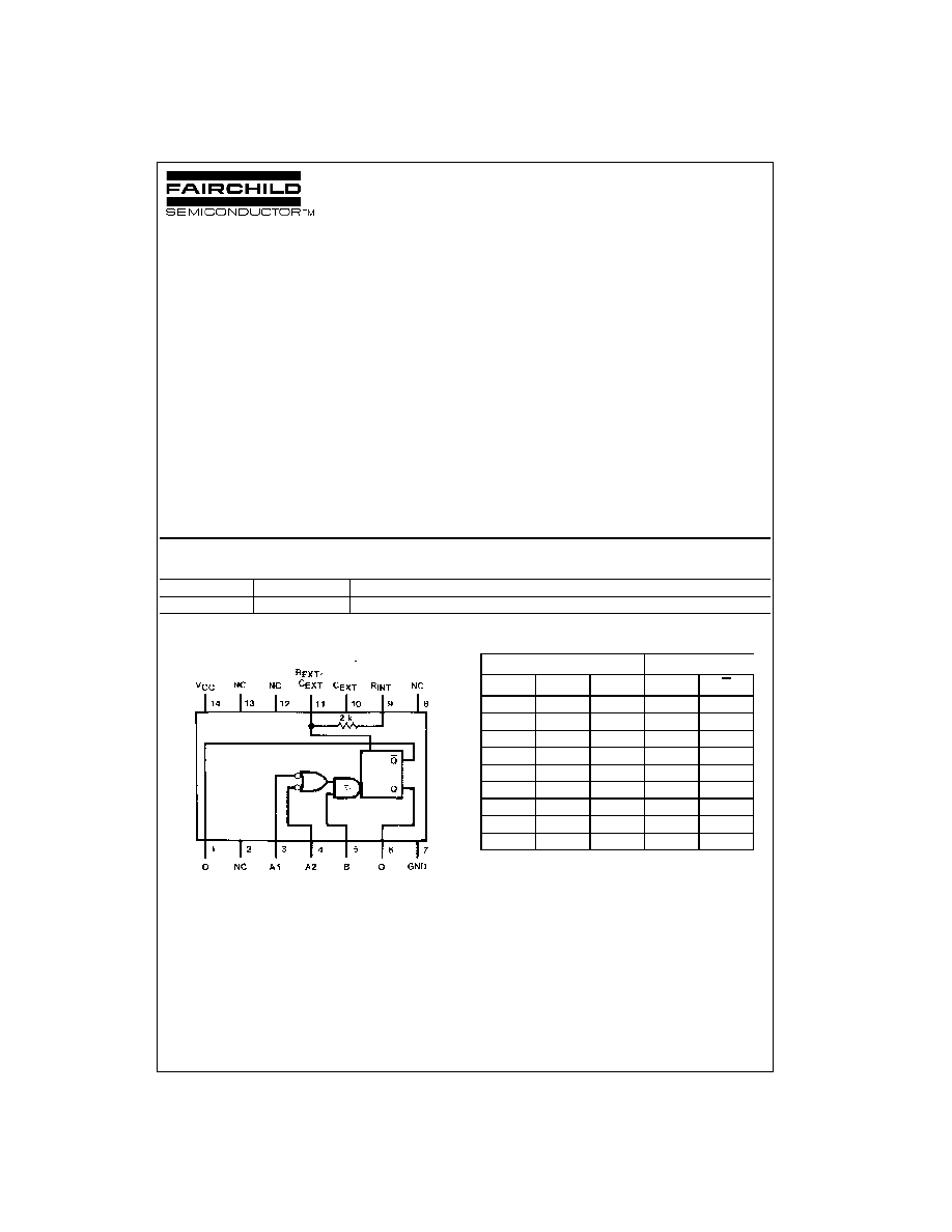
One-Shot with Clear and Complementary Outputs
General Description
The DM74121 is a monostable multivibrator featuring both
positive and negative edge triggering with complementary
outputs. An internal 2k
timing resistor is provided for
design convenience minimizing component count and lay-
out problems. this device can be used with a single exter-
nal capacitor. Inputs (A) are active-LOW trigger transition
inputs and input (B) is and active-HIGH transition Schmitt-
trigger input that allows jitter-free triggering from inputs with
transition rates as slow as 1 volt/second. A high immunity
to V
CC
noise of typically 1.5V is also provided by internal
circuitry at the input stage.
To obtain optimum and trouble free operation please read
operating rules and one-shot application notes carefully
and observe recommendations.
Features
s
Triggered from active-HIGH transition or active-LOW
transition inputs
s
Variable pulse width from 30 ns to 28 seconds
s
Jitter free Schmitt-trigger input
s
Excellent noise immunity typically 1.2V
s
Stable pulse width up to 90% duty cycle
s
TTL, DTL compatible
s
Compensated for V
CC
and temperature variations
s
Input clamp diodes
Ordering Code:
Connection Diagram
Function Table
H
=
HIGH Logic Level
=
Positive Going Transition
L
=
LOW Logic Level
=
Negative Going Transition
X
=
Can Be Either LOW or HIGH
�
=
A Positive Pulse
=
A Negative Pulse
Functional Description
The basic output pulse width is determined by selection of
an internal resistor R
INT
or an external resistor (R
X
) and
capacitor (C
X
). Once triggered the output pulse width is
independent of further transitions of the inputs and is func-
tion of the timing components. Pulse width can vary from a
few nano-seconds to 28 seconds by choosing appropriate
R
X
and C
X
combinations. There are three trigger inputs
from the device, two negative edge-triggering (A) inputs,
one positive edge Schmitt-triggering (B) input.
Order Number
Package Number
Package Description
DM74121N
N14A
14-Lead Plastic Dual-In-Line Package (PDIP), JEDEC MS-001, 0.300 Wide
Inputs
Outputs
A1
A2
B
Q
Q
L
X
H
L
H
X
L
H
L
H
X
X
L
L
H
H
H
X
L
H
H
H
�
H
H
�
H
�
L
X
�
X
L
�

www.fairchildsemi.com
2
DM74121
Operating Rules
1. To use the internal 2 k
timing resistor, connect the
R
INT
pin to V
CC
.
2. An external resistor (R
X
) or the internal resistor (2 k
)
and an external capacitor (C
X
) are required for proper
operation. The value of C
X
may vary from 0 to any nec-
essary value. For small time constants use high-quality
mica, glass, polypropylene, polycarbonate, or polysty-
rene capacitors. For large time constants use solid tan-
talum or special aluminum capacitors. If the timing
capacitors have leakages approaching 100 nA or if
stray capacitance from either terminal to ground is
greater than 50 pF the timing equations may not repre-
sent the pulse width the device generates.
3. The pulse width is essentially determined by external
timing components R
X
and C
X
. For C
X
<
1000 pF see
Figure 1 design curves on t
W
as function of timing com-
ponents value. For C
X
>
1000 pF the output is defined
as:
t
W
=
K R
X
C
X
where [R
X
is in Kilo-ohm]
[C
X
is in pico Farad]
[t
W
is in nano second]
[K
0.7]
4. If C
X
is an electrolytic capacitor a switching diode is
often required for standard TTL one-shots to prevent
high inverse leakage current Figure 2.
5. Output pulse width versus V
CC
and operation tempera-
tures: Figure 3 depicts the relationship between pulse
width variation versus V
CC.
Figure 4 depicts pulse
width variation versus ambient temperature.
6. The "K" coefficient is not a constant, but varies as a
function of the timing capacitor C
X
. Figure 5 details this
characteristic.
7. Under any operating condition C
X
and R
X
must be kept
as close to the one-shot device pins as possible to min-
imize stray capacitance, to reduce noise pick-up, and
to reduce I X R and Ldi/dt voltage developed along
their connecting paths. If the lead length from C
X
to
pins (10) and (11) is greater than 3 cm, for example,
the output pulse width might be quite different from val-
ues predicted from the appropriate equations. A non-
inductive and low capacitive path is necessary to
ensure complete discharge of C
X
in each cycle of its
operation so that the output pulse width will be accu-
rate.
8. V
CC
and ground wiring should conform to good high-
frequency standards and practices so that switching
transients on the V
CC
and ground return leads do not
cause interaction between one-shots. A 0.01
µ
F to 0.10
µ
F bypass capacitor (disk ceramic or monolithic type)
from V
CC
to ground is necessary on each device. Fur-
thermore, the bypass capacitor should be located as
close to the V
CC
-pin as space permits.
For further detailed device characteristics and output per-
formance please refer to the one-shot application note, AN-
366.
FIGURE 1.
FIGURE 2.
FIGURE 3.
FIGURE 4.
FIGURE 5.
3
www.fairchildsemi.com
DM74121
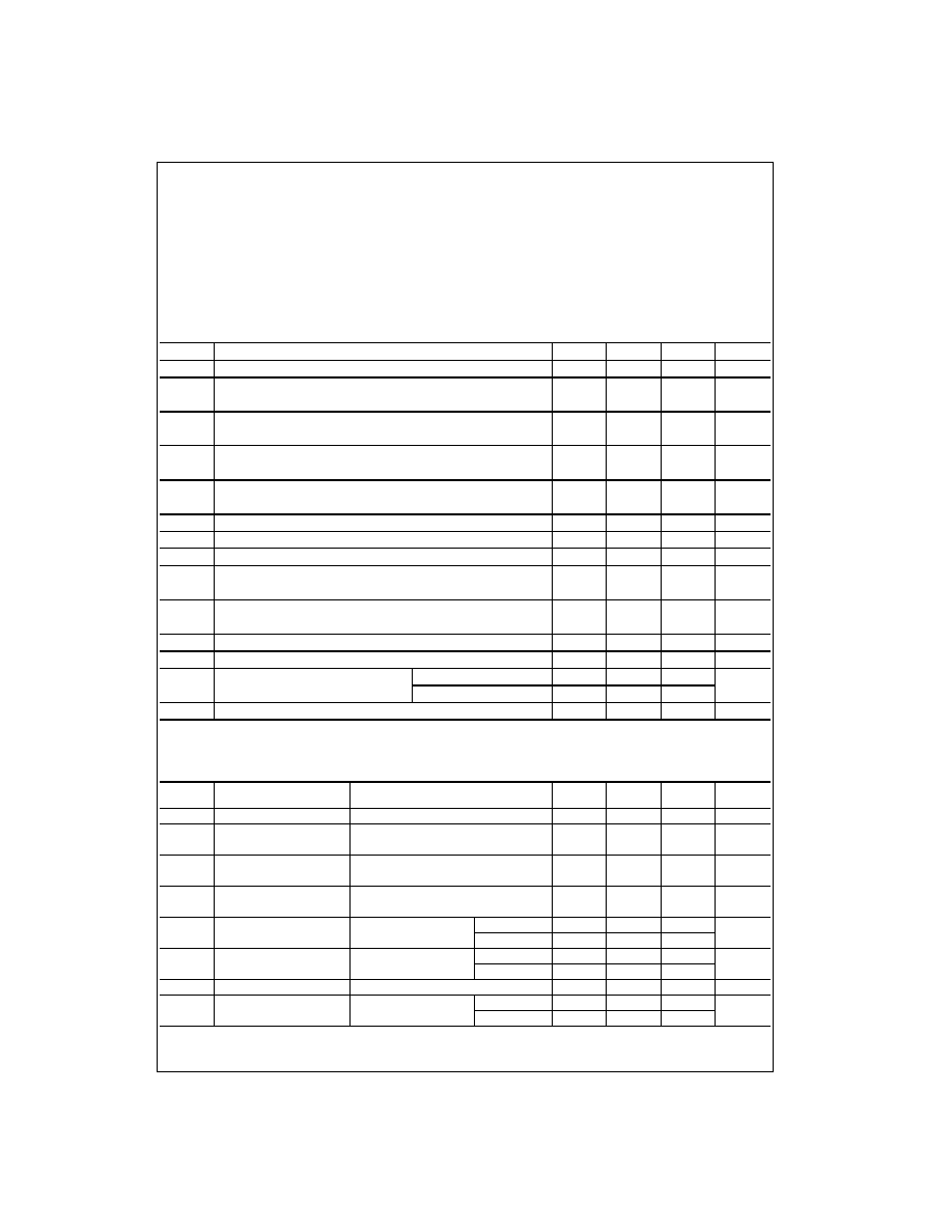
Absolute Maximum Ratings
(Note 1)
Note 1: The Absolute Maximum Ratings are those values beyond which
the safety of the device cannot be guaranteed. The device should not be
operated at these limits. The parametric values defined in the Electrical
Characteristics tables are not guaranteed at the absolute maximum ratings.
The Recommended Operating Conditions table will define the conditions
for actual device operation.
Recommended Operating Conditions
Note 2: T
A
=
25
∞
C and V
CC
=
5V
Electrical Characteristics
over recommended operating free air temperature range (unless otherwise noted)
Note 3: All typicals are at V
CC
=
5V, T
A
=
25
∞
C.
Note 4: Not more than one output should be shorted at a time.
Supply Voltage
7V
Input Voltage
5.5V
Operating Free Air Temperature Range
0
∞
C to
+
70
∞
C
Storage Temperature Range
-
65
∞
C to
+
150
∞
C
Symbol
Parameter
Min
Nom
Max
Units
V
CC
Supply Voltage
4.75
5
5.25
V
V
T
+
Positive-Going Input Threshold Voltage
1.4
2
V
at the A Input (V
CC
=
Min)
V
T
-
Negative-Going Input Threshold Voltage
0.8
1.4
V
at the A Input (V
CC
=
Min)
V
T
+
Positive-Going Input Threshold Voltage
1.5
2
V
at the B Input (V
CC
=
Min)
V
T
-
Negative-Going Input Threshold Voltage
0.8
1.3
V
at the B Input (V
CC
=
Min)
I
OH
HIGH Level Output Current
-
0.4
mA
I
OL
LOW Level Output Current
16
mA
t
W
Input Pulse Width (Note 2)
40
ns
dV/dt
Rate of Rise or Fall of
1
V/s
Schmidt Input (B) (Note 2)
dV/dt
Rate of Rise or Fall of
1
V/
µ
s
Schmidt Input (A) (Note 2)
R
EXT
External Timing Resistor (Note 2)
1.4
40
k
C
EXT
External Timing Capacitance (Note 2)
0
1000
µ
F
DC
Duty Cycle (Note 2)
R
T
=
2 k
67
%
R
T
=
R
EXT
(Max)
90
T
A
Free Air Operating Temperature
0
70
∞
C
Symbol
Parameter
Conditions
Min
Typ
(Note 3)
Max
Units
V
I
Input Clamp Voltage
V
CC
=
Min, I
I
=
-
12 mA
-
1.5
V
V
OH
HIGH Level Output
V
CC
=
Min, I
OH
=
Max,
2.4
3.4
V
Voltage
V
IL
=
Max, V
IH
=
Min
V
OL
LOW Level Output
V
CC
=
Min, I
OL
=
Max,
0.2
0.4
V
Voltage
V
IH
=
Max, V
IL
=
Min
I
I
Input Current @
V
CC
=
Max, V
I
=
5.5V
1
mA
Max Input Voltage
I
IH
HIGH Level
V
CC
=
Max,
A1, A2
40
µ
A
Input Current
V
I
=
2.4V
B
80
I
IL
LOW Level
V
CC
=
Max,
A1, A2
-
1.6
mA
Input Current
V
I
=
0.4V
B
-
3.2
I
OS
Short Circuit Output Current
V
CC
=
Max (Note 4)
-
18
-
55
mA
I
CC
Supply Current
V
CC
=
Max
Quiescent
13
25
mA
Triggered
23
40
www.fairchildsemi.com
4
DM74121
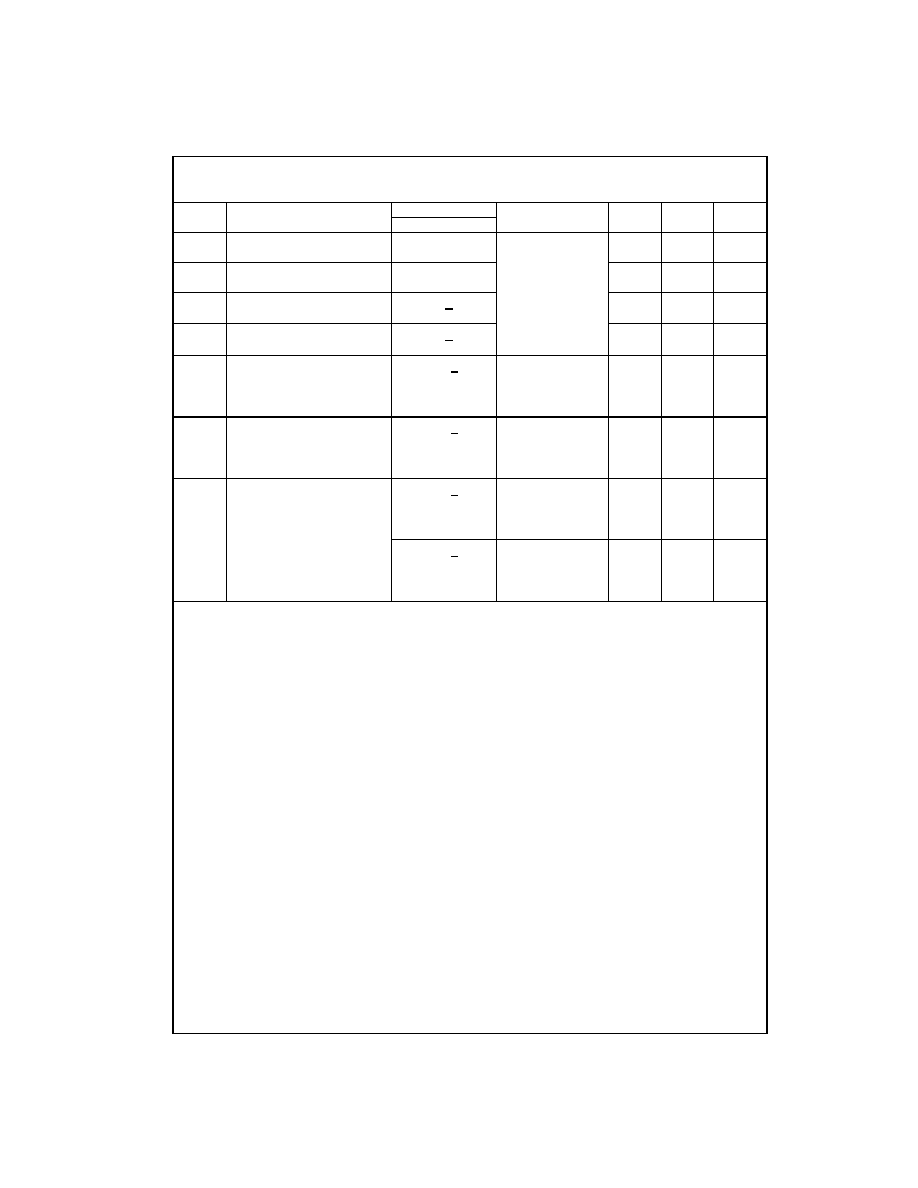
Switching Characteristics
At V
CC
=
5V and T
A
=
25
∞
C (See Test Waveforms and Output Load Section)
Symbol
Parameter
From (Input)
Conditions
Min
Max
Units
To (Output)
t
PLH
Propagation Delay Time
A1, A2
C
EXT
=
80 pF
70
ns
LOW-to-HIGH Level Output
to Q
R
INT
to V
CC
t
PLH
Propagation Delay Time
B to
C
L
=
15 pF
55
ns
LOW-to-HIGH Level Output
Q
R
L
=
400
t
PHL
Propagation Delay Time
A1, A2
80
ns
HIGH-to-LOW Level Output
to Q
t
PHL
Propagation Delay Time
B
65
ns
HIGH-to-LOW Level Output
to Q
t
W(OUT)
Output Pulse
A1, A2 or B
C
EXT
=
80 pF
70
150
ns
Width Using the
to Q, Q
R
INT
to V
CC
Internal Timing Resistor
R
L
=
400
C
L
=
15 pF
t
W(OUT)
Output Pulse
A1, A2
C
EXT
=
0 pF
50
ns
Width Using Zero
to Q, Q
R
INT
to V
CC
Timing Capacitance
R
L
=
400
C
L
=
15 pF
t
W(OUT)
Output Pulse
A1, A2
C
EXT
=
100pF
600
800
ns
Width Using External
to Q, Q
R
INT
=
10 k
Timing Resistor
R
L
=
400
C
L
=
15pF
A1, A2
C
EXT
=
1
µ
F
6
8
ms
to Q, Q
R
INT
=
10 k
R
L
=
400
C
L
=
15 pF
5
www.fairchildsemi.com
DM74121
One-
S
h
ot
w
i
th
Cl
ear
and Compl
e
m
e
nt
ary
Outpu
t
s
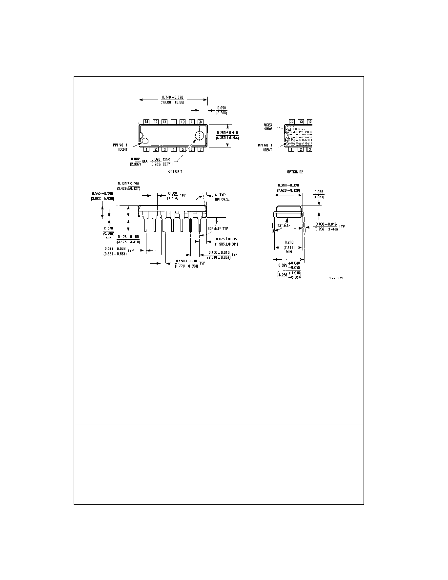
Physical Dimensions
inches (millimeters) unless otherwise noted
14-Lead Plastic Dual-In-Line Package (PDIP), JEDEC MS-001, 0.300 Wide
Package Number N14A
Fairchild does not assume any responsibility for use of any circuitry described, no circuit patent licenses are implied and
Fairchild reserves the right at any time without notice to change said circuitry and specifications.
LIFE SUPPORT POLICY
FAIRCHILD'S PRODUCTS ARE NOT AUTHORIZED FOR USE AS CRITICAL COMPONENTS IN LIFE SUPPORT
DEVICES OR SYSTEMS WITHOUT THE EXPRESS WRITTEN APPROVAL OF THE PRESIDENT OF FAIRCHILD
SEMICONDUCTOR CORPORATION. As used herein:
1. Life support devices or systems are devices or systems
which, (a) are intended for surgical implant into the
body, or (b) support or sustain life, and (c) whose failure
to perform when properly used in accordance with
instructions for use provided in the labeling, can be rea-
sonably expected to result in a significant injury to the
user.
2. A critical component in any component of a life support
device or system whose failure to perform can be rea-
sonably expected to cause the failure of the life support
device or system, or to affect its safety or effectiveness.
www.fairchildsemi.com