© 2000 Fairchild Semiconductor Corporation
DS006391
www.fairchildsemi.com
August 1986
Revised March 2000
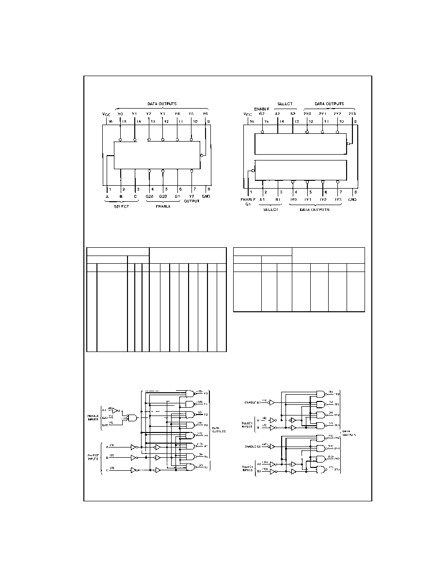
DM74LS138
∑ D
M
74LS13
9
Decode
r/Demul
t
i
p
lex
e
r
DM74LS138 ∑ DM74LS139
Decoder/Demultiplexer
General Description
These Schottky-clamped circuits are designed to be used
in high-performance memory-decoding or data-routing
applications, requiring very short propagation delay times.
In high-performance memory systems these decoders can
be used to minimize the effects of system decoding. When
used with high-speed memories, the delay times of these
decoders are usually less than the typical access time of
the memory. This means that the effective system delay
introduced by the decoder is negligible.
The DM74LS138 decodes one-of-eight lines, based upon
the conditions at the three binary select inputs and the
three enable inputs. Two active-low and one active-high
enable inputs reduce the need for external gates or invert-
ers when expanding. A 24-line decoder can be imple-
mented with no external inverters, and a 32-line decoder
requires only one inverter. An enable input can be used as
a data input for demultiplexing applications.
The DM74LS139 comprises two separate two-line-to-four-
line decoders in a single package. The active-low enable
input can be used as a data line in demultiplexing applica-
tions.
All of these decoders/demultiplexers feature fully buffered
inputs, presenting only one normalized load to its driving
circuit. All inputs are clamped with high-performance
Schottky diodes to suppress line-ringing and simplify sys-
tem design.
Features
s
Designed specifically for high speed:
Memory decoders
Data transmission systems
s
DM74LS138 3-to-8-line decoders incorporates 3 enable
inputs to simplify cascading and/or data reception
s
DM74LS139 contains two fully independent 2-to-4-line
decoders/demultiplexers
s
Schottky clamped for high performance
s
Typical propagation delay (3 levels of logic)
DM74LS138
21 ns
DM74LS139
21 ns
s
Typical power dissipation
DM74LS138
32 mW
DM74LS139
34 mW
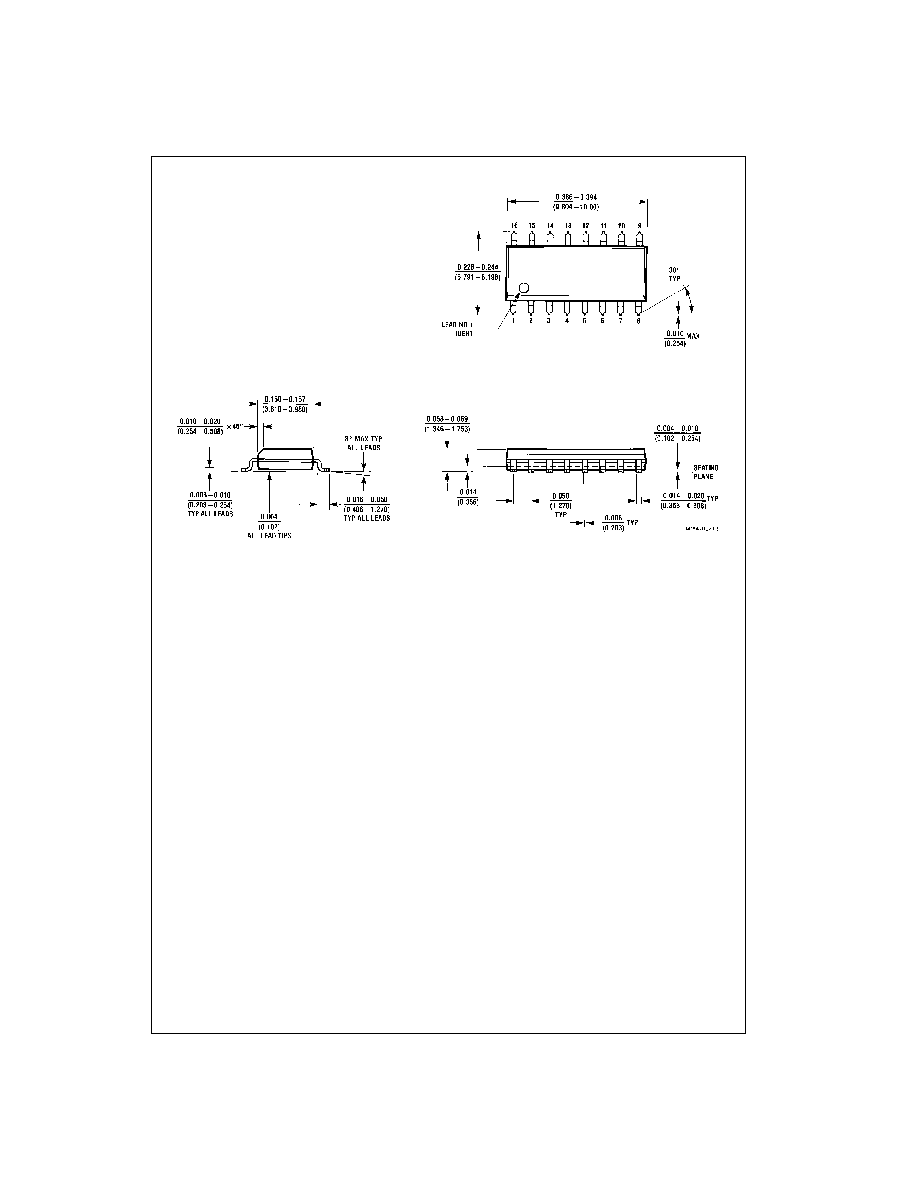
Ordering Code:
Devices also available in Tape and Reel. Specify by appending the suffix letter "X" to the ordering code.
Order Number
Package Number
Package Description
DM74LS138M
M16A
16-Lead Small Outline Integrated Circuit (SOIC), JEDEC MS-012, 0.150 Narrow
DM74LS138SJ
M16D
16-Lead Small Outline Package (SOP), EIAJ TYPE II, 5.3mm Wide
DM74LS138N
N16E
16-Lead Plastic Dual-In-Line Package (PDIP), JEDEC MS-001, 0.300 Wide
DM74LS139M
M16A
16-Lead Small Outline Integrated Circuit (SOIC), JEDEC MS-012, 0.150 Narrow
DM74LS139SJ
M16D
16-Lead Small Outline Package (SOP), EIAJ TYPE II, 5.3mm Wide
DM74LS139N
N16E
16-Lead Plastic Dual-In-Line Package (PDIP), JEDEC MS-001, 0.300 Wide
3
www.fairchildsemi.com
DM74LS138
∑ D
M
74LS13
9
Absolute Maximum Ratings
(Note 2)
Note 2: The "Absolute Maximum Ratings" are those values beyond which
the safety of the device cannot be guaranteed. The device should not be
operated at these limits. The parametric values defined in the Electrical
Characteristics tables are not guaranteed at the absolute maximum ratings.
The "Recommended Operating Conditions" table will define the conditions
for actual device operation.
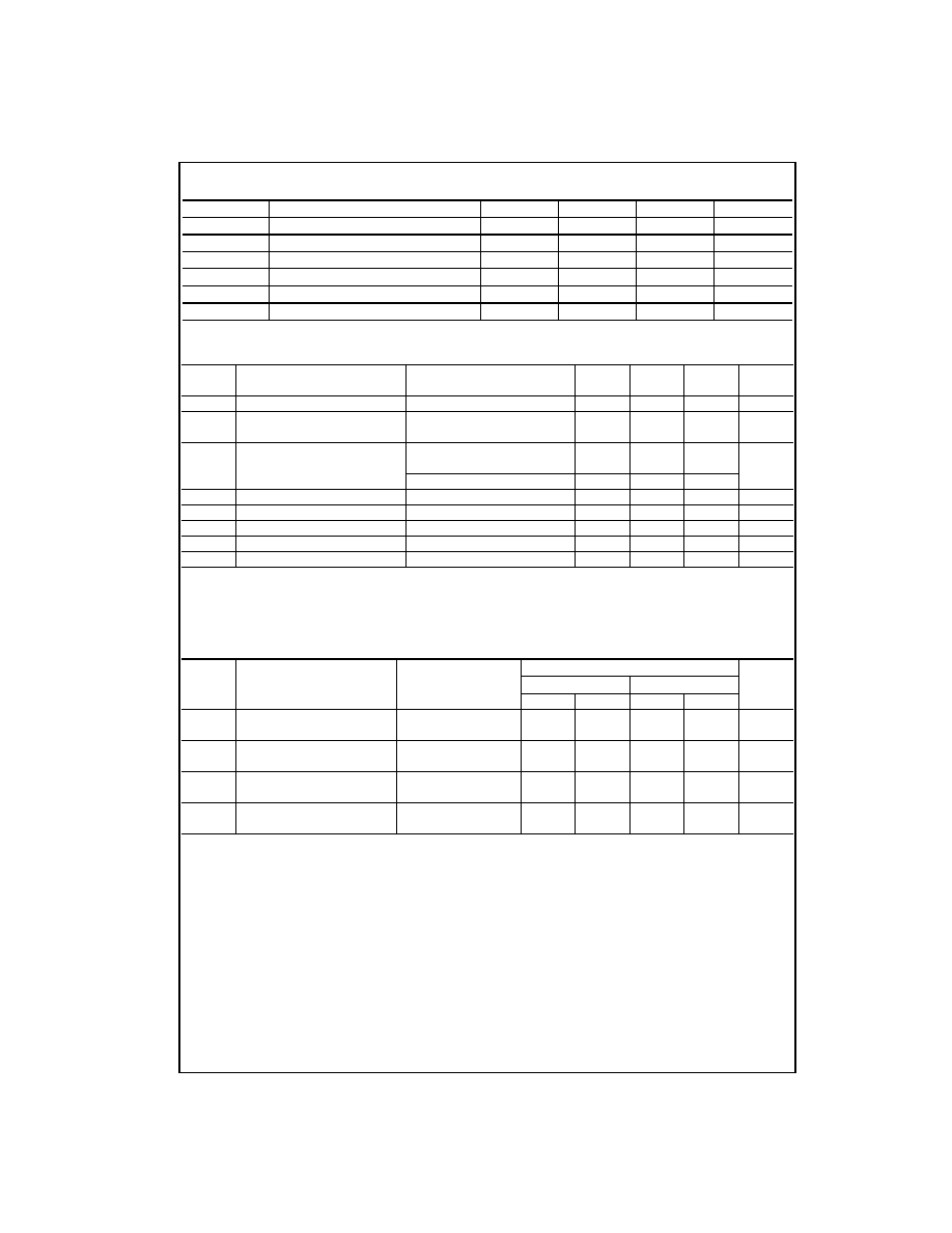
DM74LS138 Recommended Operating Conditions
DM74LS138 Electrical Characteristics
over recommended operating free air temperature range (unless otherwise noted)
Note 3: All typicals are at V
CC
=
5V, T
A
=
25
∞
C.
Note 4: Not more than one output should be shorted at a time, and the duration should not exceed one second.
Note 5: I
CC
is measured with all outputs enabled and OPEN.
DM74LS138 Switching Characteristics
at V
CC
=
5V and T
A
=
25
∞
C
Supply Voltage
7V
Input Voltage
7V
Operating Free Air Temperature Range
0
∞
C to
+
70
∞
C
Storage Temperature Range
-
65
∞
C to
+
150
∞
C
Symbol
Parameter
Min
Nom
Max
Units
V
CC
Supply Voltage
4.75
5
5.25
V
V
IH
HIGH Level Input Voltage
2
V
V
IL
LOW Level Input Voltage
0.8
V
I
OH
HIGH Level Output Current
-
0.4
mA
I
OL
LOW Level Output Current
8
mA
T
A
Free Air Operating Temperature
0
70
∞
C
Symbol
Parameter
Conditions
Min
Typ
Max
Units
(Note 3)
V
I
Input Clamp Voltage
V
CC
=
Min, I
I
=
-
18 mA
-
1.5
V
V
OH
HIGH Level Output Voltage
V
CC
=
Min, I
OH
=
Max, V
IL
=
Max, V
IH
=
Min
2.7
3.4
V
V
OL
LOW
Level V
CC
=
Min, I
OL
=
Max, V
IL
=
Max, V
IH
=
Min
0.35
0.5
V
Output Voltage
I
OL
=
4 mA, V
CC
=
Min
0.25
0.4
I
I
Input Current @ Max Input Voltage
V
CC
=
Max, V
I
=
7V
0.1
mA
I
IH
HIGH Level Input Current
V
CC
=
Max, V
I
=
2.7V
20
µ
A
I
IL
LOW Level Input Current
V
CC
=
Max, V
I
=
0.4V
-
0.36
mA
I
OS
Short Circuit Output Current
V
CC
=
Max (Note 4)
-
20
-
100
mA
I
CC
Supply Current
V
CC
=
Max (Note 5)
6.3
10
mA
From (Input)
Levels
R
L
=
2 k
Symbol
Parameter
To (Output)
of Delay
C
L
=
15 pF
C
L
=
50 pF
Units
Min
Max
Min
Max
t
PLH
Propagation Delay Time
Select to Output
2
18
27
ns
LOW-to-HIGH Level Output
t
PHL
Propagation Delay Time
Select to Output
2
27
40
ns
HIGH-to-LOW Level Output
t
PLH
Propagation Delay Time
Select to Output
3
18
27
ns
LOW-to-HIGH Level Output
t
PHL
Propagation Delay Time
Select to Output
3
27
40
ns
HIGH-to-LOW Level Output
t
PLH
Propagation Delay Time
Enable to Output
2
18
27
ns
LOW-to-HIGH Level Output
t
PHL
Propagation Delay Time
Enable to Output
2
24
40
ns
HIGH-to-LOW Level Output
t
PLH
Propagation Delay Time
Enable to Output
3
18
27
ns
LOW-to-HIGH Level Output
t
PHL
Propagation Delay Time
Enable to Output
3
28
40
ns
HIGH-to-LOW Level Output
www.fairchildsemi.com
4
DM74LS138
∑ DM74LS139
DM74LS139 Recommended Operating Conditions
DM74LS139 Electrical Characteristics
over recommended operating free air temperature range (unless otherwise noted)
Note 6: All typicals are at V
CC
=
5V, T
A
=
25
∞
C.
Note 7: Not more than one output should be shorted at a time, and the duration should not exceed one second.
Note 8: I
CC
is measured with all outputs enabled and OPEN.
DM74LS139 Switching Characteristics
at V
CC
=
5V and T
A
=
25
∞
C
Symbol
Parameter
Min
Nom
Max
Units
V
CC
Supply Voltage
4.75
5
5.25
V
V
IH
HIGH Level Input Voltage
2
V
V
IL
LOW Level Input Voltage
0.8
V
I
OH
HIGH Level Output Current
-
0.4
mA
I
OL
LOW Level Output Current
8
mA
T
A
Free Air Operating Temperature
0
70
∞
C
Symbol
Parameter
Conditions
Min
Typ
Max
Units
(Note 6)
V
I
Input Clamp Voltage
V
CC
=
Min, I
I
=
-
18 mA
-
1.5
V
V
OH
HIGH Level
V
CC
=
Min, I
OH
=
Max,
2.7
3.4
V
Output Voltage
V
IL
=
Max, V
IH
=
Min
V
OL
LOW
Level V
CC
=
Min, I
OL
=
Max
0.35
0.5
Output Voltage
V
IL
=
Max, V
IH
=
Min
V
I
OL
=
4 mA, V
CC
=
Min
0.25
0.4
I
I
Input Current @ Max Input Voltage
V
CC
=
Max, V
I
=
7V
0.1
mA
I
IH
HIGH Level Input Current
V
CC
=
Max, V
I
=
2.7V
20
µ
A
I
IL
LOW Level Input Current
V
CC
=
Max, V
I
=
0.4V
-
0.36
mA
I
OS
Short Circuit Output Current
V
CC
=
Max (Note 7)
-
20
-
100
mA
I
CC
Supply Current
V
CC
=
Max (Note 8)
6.8
11
mA
From (Input)
R
L
=
2 k
Symbol
Parameter
To (Output)
C
L
=
15 pF
C
L
=
50 pF
Units
Min
Max
Min
Max
t
PLH
Propagation Delay Time
Select to Output
18
27
ns
LOW-to-HIGH Level Output
t
PHL
Propagation Delay Time
Select to Output
27
40
ns
HIGH-to-LOW Level Output
t
PLH
Propagation Delay Time
Enable to Output
18
27
ns
LOW-to-HIGH Level Output
t
PHL
Propagation Delay Time
Enable to Output
24
40
ns
HIGH-to-LOW Level Output