© 2000 Fairchild Semiconductor Corporation
DS006406
www.fairchildsemi.com
September 1986
Revised March 2000
DM74LS193
Synchr
onous 4-Bi
t Binar
y
Count
er wit
h
Dual
C
l
ock
DM74LS193
Synchronous 4-Bit Binary Counter with Dual Clock
General Description
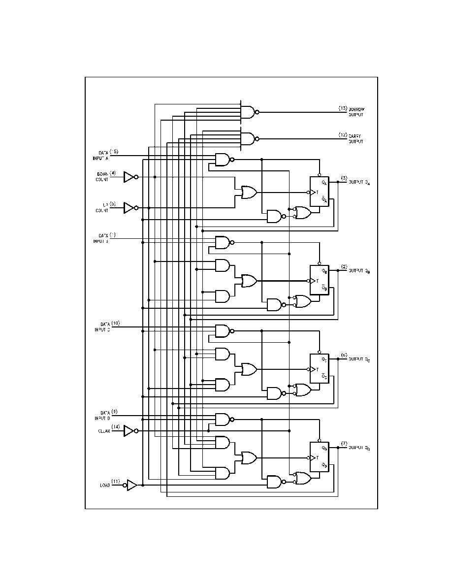
The DM74LS193 circuit is a synchronous up/down 4-bit
binary counter. Synchronous operation is provided by hav-
ing all flip-flops clocked simultaneously, so that the outputs
change together when so instructed by the steering logic.
This mode of operation eliminates the output counting
spikes normally associated with asynchronous (ripple-
clock) counters.
The outputs of the four master-slave flip-flops are triggered
by a LOW-to-HIGH level transition of either count (clock)
input. The direction of counting is determined by which
count input is pulsed while the other count input is held
HIGH.
The counter is fully programmable; that is, each output may
be preset to either level by entering the desired data at the
inputs while the load input is LOW. The output will change
independently of the count pulses. This feature allows the
counters to be used as modulo-N dividers by simply modi-
fying the count length with the preset inputs.
A clear input has been provided which, when taken to a
high level, forces all outputs to the low level; independent
of the count and load inputs. The clear, count, and load
inputs are buffered to lower the drive requirements of clock
drivers, etc., required for long words.
These counters were designed to be cascaded without the
need for external circuitry. Both borrow and carry outputs
are available to cascade both the up and down counting
functions. The borrow output produces a pulse equal in
width to the count down input when the counter underflows.
Similarly, the carry output produces a pulse equal in width
to the count down input when an overflow condition exists.
The counters can then be easily cascaded by feeding the
borrow and carry outputs to the count down and count up
inputs respectively of the succeeding counter.
Features
s
Fully independent clear input
s
Synchronous operation
s
Cascading circuitry provided internally
s
Individual preset each flip-flop
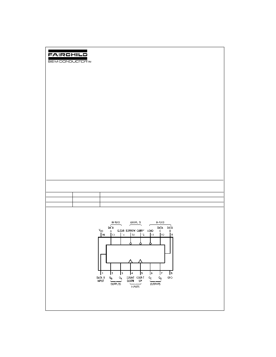
Ordering Code:
Connection Diagram
Order Number
Package Number
Package Description
DM74LS193M
M16A
16-Lead Small Outline Integrated Circuit (SOIC), JEDEC MS-012, 0.150" Narrow Body
DM74LS193N
N16E
16-Lead Plastic Dual-In-Line Package (PDIP), JEDEC MS-001, 0.300" Wide
3
www.fairchildsemi.com
DM74LS193
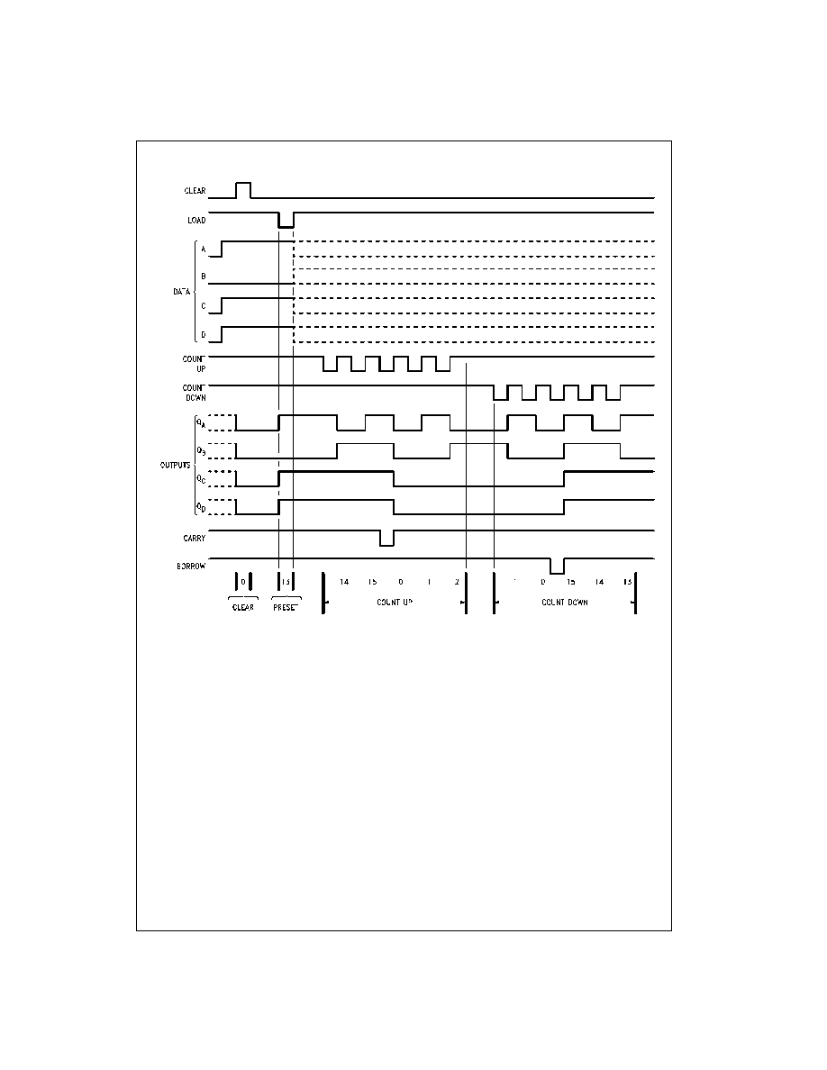
Timing Diagram
Note A: Clear overrides load, data, and count inputs
Note B: When counting up, count-down input must be HIGH; when counting down, count-up input must be HIGH.
www.fairchildsemi.com
4
DM74LS193
Absolute Maximum Ratings
(Note 1)
Note 1: The "Absolute Maximum Ratings" are those values beyond which
the safety of the device cannot be guaranteed. The device should not be
operated at these limits. The parametric values defined in the Electrical
Characteristics tables are not guaranteed at the absolute maximum ratings.
The "Recommended Operating Conditions" table will define the conditions
for actual device operation.
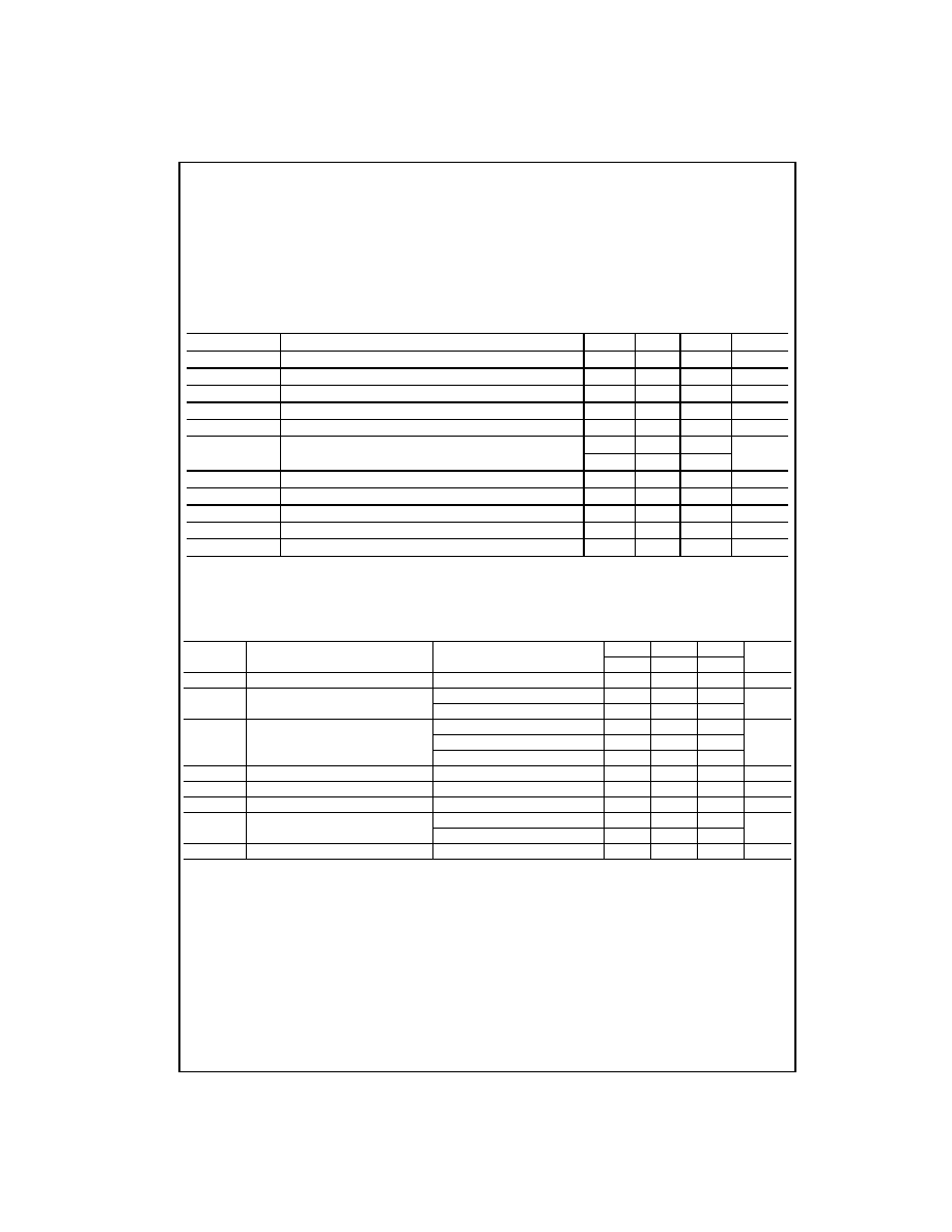
Recommended Operating Conditions
Note 2: C
L
=
15 pF, R
L
=
2 k
, I
A
=
25
∞
C and V
CC
=
5V.
Note 3: C
L
=
50 pF, R
L
=
2 k
, I
A
=
25
∞
C and V
CC
=
5V.
Note 4: T
A
=
25
∞
C and V
CC
=
5V.
DC Electrical Characteristics
Note 5: All typicals are at V
CC
=
5V, T
A
=
25
∞
C.
Note 6: Not more than one output should be shorted at a time, and the duration should not exceed one second.
Note 7: I
CC
is measured with all outputs open, CLEAR and LOAD inputs grounded, and all other inputs at 4.5V.
Operating Free Air Temperature Range
-
0
∞
C to
+
70
∞
C
Supply Voltage
7V
Input Voltage
7V
Storage Temperature Range
-
65
∞
C to
+
125
∞
C
Symbol
Parameter
Min
Nom
Max
Units
V
CC
Supply Voltage
4.75
5
5.25
V
V
IH
HIGH Level Input Voltage
2
V
V
IL
LOW Level Input Voltage
0.8
V
I
OH
HIGH Level Output Current
-
0.4
mA
I
OL
LOW Level Output Current
8
mA
f
CLK
Clock Frequency (Note 2)
0
25
MHz
Clock Frequency (Note 3)
t
W
Pulse Width of any Input (Note 4)
20
ns
t
SU
Data Setup Time (Note 4)
20
ns
t
H
Data Hold Time (Note 4)
0
ns
t
EN
Enable Time to Clock (Note 4)
40
ns
T
A
Free Air Operating Temperature
0
70
∞
C
Symbol
Parameter
Conditions
Min
Typ
Max
Units
(Note 5)
V
I
Input Clamp Voltage
V
CC
=
Min, I
I
=
-
18 mA
-
1.5
V
V
OH
HIGH Level Output
V
CC
=
Min, I
OH
=
Max
2.5
3.4
V
Voltage
V
IL
=
Max, V
IH
=
Min
2.7
3.4
V
OL
LOW Level Output
V
CC
=
Min, I
OL
=
Max
0.25
0.4
Voltage
V
IL
=
Max, V
IH
=
Min
0.35
0.5
V
I
OL
=
4 mA, V
CC
=
Min
0.25
0.4
I
I
Input Current @ Max Input Voltage
V
CC
=
Max, V
I
=
7V
0.1
mA
I
IH
HIGH Level Input Current
V
CC
=
Max, V
I
=
2.7V
20
µ
A
I
IL
LOW Level Input Current
V
CC
=
Max, V
I
=
0.4V
-
0.4
mA
I
OS
Short Circuit
V
CC
=
Max
-
20
-
100
mA
Output Current
(Note 6)
-
20
-
100
I
CC
Supply Current
V
CC
=
Max (Note 7)
19
34
mA