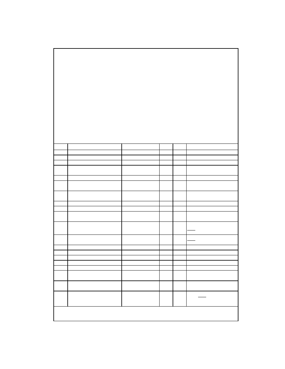
 | –≠–ª–µ–∫—Ç—Ä–æ–Ω–Ω—ã–π –∫–æ–º–ø–æ–Ω–µ–Ω—Ç: 74ABT652 | –°–∫–∞—á–∞—Ç—å:  PDF PDF  ZIP ZIP |

November 1992
Revised January 1999
7
4
AB
T6
52
Oct
a
l T
r
anscei
ver
s
and Regi
ster
s w
i
th
3-
ST
A
T
E O
u
t
put
s
© 1999 Fairchild Semiconductor Corporation
DS011512.prf
www.fairchildsemi.com
74ABT652
Octal Transceivers and Registers with 3-STATE Outputs
General Description
The ABT652 consists of bus transceiver circuits with D-
type flip-flops and control circuitry arranged for multiplexed
transmission of data directly from the input bus or from the
internal registers. Data on the A or B bus will be clocked
into the registers as the appropriate clock pin goes to HIGH
logic level. Output Enable pins (OEAB, OEBA) are pro-
vided to control the transceiver function.
Features
s
Independent registers for A and B buses
s
Multiplexed real-time and stored data
s
A and B output sink capability of 64 mA, source
capability of 32 mA
s
Guaranteed output skew
s
Guaranteed multiple output switching specifications
s
Output switching specified for both 50 pF and
250 pF loads
s
Guaranteed simultaneous switching noise level and
dynamic threshold performance
s
Guaranteed latchup protection
s
High impedance glitch free bus loading during entire
power up and power down cycle
s
Nondestructive hot insertion capability
Ordering Code:
Devices also available in Tape and Reel. Specify by appending the suffix letter "X" to the ordering code.
Connection Diagram
Pin Assignment for
SOIC, SSOP and TSSOP
Pin Descriptions
Order Number
Package Number
Package Description
74ABT652CSC M24B
24-Lead Small Outline Integrated Circuit (SOIC), JEDEC MS-013, 0.300" Wide Body
74ABT652CMSA
MSA24
24-Lead Shrink Small Outline Package (SSOP), EIAJ TYPE II, 5.3mm Wide
74ABT652CMTC
MTC24
24-Lead Thin Shrink Small Outline Package (TSSOP), JEDEC MO-153, 4.4mm Wide
Pin Names
Description
A
0
≠A
7
Data Register A Inputs/3-STATE Outputs
B
0
≠B
7
Data Register B Inputs/3-STATE Outputs
CPAB, CPBA
Clock Pulse Inputs
SAB, SBA
Select Inputs
OEAB, OEBA Output Enable Inputs

www.fairchildsemi.com
2
74ABT652
Truth Table
H
=
HIGH Voltage Level
L
=
LOW Voltage Level
X
=
Immaterial
=
LOW to HIGH Clock Transition
Note 1: The data output functions may be enabled or disabled by various signals at OEAB or OEBA inputs. Data input functions are always enabled, i.e.,
data at the bus pins will be stored on every LOW to HIGH transition on the clock inputs.
Functional Description
In the transceiver mode, data present at the HIGH imped-
ance port may be stored in either the A or B register or
both.
The select (SAB, SBA) controls can multiplex stored and
real-time.
The examples in Figure 1 demonstrate the four fundamen-
tal bus-management functions that can be performed with
the ABT652.
Data on the A or B data bus, or both, can be stored in the
internal D flip-flop by LOW to HIGH transitions at the
appropriate Clock Inputs (CPAB, CPBA) regardless of the
Select or Output Enable Inputs. When SAB and SBA are in
the real time transfer mode, it is also possible to store data
without using the internal D flip-flops by simultaneously
enabling OEAB and OEBA. In this configuration each Out-
put reinforces its Input. Thus when all other data sources to
the two sets of bus lines are in a HIGH impedance state,
each set of bus lines will remain at its last state.
Logic Diagram
Please note that this diagram is provided only for the understanding of logic operations and should not be used to estimate propagation delays.
Inputs
Inputs/Outputs (Note 1)
Operating Mode
OEAB
OEBA
CPAB
CPBA
SAB
SBA
A
0
thru A
7
B
0
thru B
7
L
H
H or L H or L
X
X
Input
Input
Isolation
L
H
X
X
Store A and B Data
X
H
H or L
X
X
Input
Not Specified Store A, Hold B
H
H
X
X
Input
Output
Store A in Both Registers
L
X
H or L
X
X
Not Specified Input
Hold A, Store B
L
L
X
X
Output
Input
Store B in Both Registers
L
L
X
X
X
L
Output
Input
Real-Time B Data to A Bus
L
L
X
H or L
X
H
Store B Data to A Bus
H
H
X
X
L
X
Input
Output
Real-Time A Data to B Bus
H
H
H or L
X
H
X
Stored A Data to B Bus
H
L
H or L H or L
H
H
Output
Output
Stored A Data to B Bus and
Stored B Data to A Bus

3
www.fairchildsemi.com
7
4
AB
T6
52
Note A: Real-Time
Transfer Bus B to Bus A
Note C: Storage
Note B: Real-Time
Transfer Bus A to Bus B
Note D: Transfer Storage
Data to A or B
FIGURE 1.
OEAB OEBA CPAB CPBA SAB SBA
L
L
X
X
X
L
OEAB OEBA CPAB CPBA SAB SBA
X
H
X
X
X
L
X
X
X
X
L
H
X
X
OEAB OEBA CPAB CPBA SAB SBA
H
H
X
X
L
X
OEAB OEBA CPAB CPBA SAB SBA
H
L
H or L H or L
H
H
www.fairchildsemi.com
4
74ABT652
Absolute Maximum Ratings
(Note 2)
Recommended Operating
Conditions
Note 2: Absolute maximum ratings are values beyond which the device
may be damaged or have its useful life impaired. Functional operation
under these conditions is not implied.
Note 3: Either voltage limit or current limit is sufficient to protect inputs.
DC Electrical Characteristics
Note 4: Guaranteed but not tested.
Note 5: For 8 outputs toggling, I
CCD
<
1.4 mA/MHz.
Note 6: Guaranteed, but not tested.
Storage Temperature
-
65
∞
C to
+
150
∞
C
Ambient Temperature under Bias
-
55
∞
C to
+
125
∞
C
Junction Temperature under Bias
-
55
∞
C to
+
150
∞
C
V
CC
Pin Potential to Ground Pin
-
0.5V to
+
7.0V
Input Voltage (Note 3)
-
0.5V to
+
7.0V
Input Current (Note 3)
-
30 mA to
+
5.0 mA
Voltage Applied to Any Output
in the Disable
or Power-Off State
-
0.5V to
+
5.5V
in the HIGH State
-
0.5V to V
CC
Current Applied to Output
in LOW State (Max)
twice the rated I
OL
(mA)
DC Latchup Source Current
-
500 mA
Over Voltage Latchup (I/O)
10V
Free Air Ambient Temperature
-
40
∞
C to
+
85
∞
C
Supply Voltage
+
4.5V to
+
5.5V
Minimum Input Edge Rate (
V/
t)
Data Input
50 mV/ns
Enable Input
20 mV/ns
Clock Input
100 mV/ns
Symbol
Parameter
Min
Typ
Max
Units
V
CC
Conditions
V
IH
Input HIGH Voltage
2.0
V
Recognized HIGH Signal
V
IL
Input LOW Voltage
0.8
V
Recognized LOW Signal
V
CD
Input Clamp Diode Voltage
-
1.2
V
Min
I
IN
=
-
18 mA (Non I/O Pins)
V
OH
Output HIGH
2.5
V
Min
I
OH
=
-
3 mA, (A
n
, B
n
)
Voltage
2.0
I
OH
=
-
32 mA, (A
n
, B
n
)
V
OL
Output LOW Voltage
0.55
V
Min
I
OL
=
64 mA, (A
n
, B
n
)
V
ID
Input Leakage Test
4.75
V
0.0
I
ID
=
1.9
µ
A, (Non-I/O Pins)
All Other Pins Grounded
I
IH
Input HIGH Current
1
µ
A
Max
V
IN
=
2.7V (Non-I/O Pins) (Note 4)
1
V
IN
=
V
CC
(Non-I/O Pins)
I
BVI
Input HIGH Current Breakdown Test
7
µ
A
Max
V
IN
=
7.0V (Non-I/O Pins)
I
BVIT
Input HIGH Current Breakdown Test (I/O)
100
µ
A
Max
V
IN
=
5.5V (A
n
, B
n
)
I
IL
Input LOW Current
-
1
µ
A
Max
V
IN
=
0.5V (Non-I/O Pins) (Note 4)
-
1
V
IN
=
0.0V (Non-I/O Pins)
I
IH
+
I
OZH
Output Leakage Current
10
µ
A
0V≠5.5V V
OUT
=
2.7V (A
n
, B
n
);
OEBA
=
2.0V and OEAB
=
GND
=
2.0V
I
IL
+
I
OZL
Output Leakage Current
-
10
µ
A
0V≠5.5V V
OUT
=
0.5V (A
n
, B
n
);
OEBA
=
2.0V and OEAB
=
GND
=
2.0V
I
OS
Output Short-Circuit Current
-
100
-
275
mA
Max
V
OUT
=
0V (A
n
, B
n
)
I
CEX
Output HIGH Leakage Current
50
µ
A
Max
V
OUT
=
V
CC
(A
n
, B
n
)
I
ZZ
Bus Drainage Test
100
µ
A
0.0V
V
OUT
=
5.5V (A
n
, B
n
); All Others GND
I
CCH
Power Supply Current
250
µ
A
Max
All Outputs HIGH
I
CCL
Power Supply Current
30
mA
Max
All Outputs LOW
I
CCZ
Power Supply Current
50
µ
A
Max
Outputs 3-STATE;
All others at V
CC
or GND
I
CCT
Additional I
CC
/Input
2.5
mA
Max
V
I
=
V
CC
-
2.1V
All others at V
CC
or GND
I
CCD
Dynamic I
CC
No Load
0.18
mA/MHz
Max
Outputs Open (Note 5)
(Note 6)
OEAB
=
OEBA
=
GND
One bit toggling, 50% duty cycle

5
www.fairchildsemi.com
7
4
AB
T6
52
DC Electrical Characteristics
(SOIC package)
Note 7: Max number of outputs defined as (n). n
-
1 data inputs are driven 0V to 3V. One output at LOW. Guaranteed, but not tested.
Note 8: Max number of outputs defined as (n). n
-
1 data inputs are driven 0V to 3V. One output HIGH. Guaranteed, but not tested.
Note 9: Max number of data inputs (n) switching. n
-
1 inputs switching 0V to 3V. Input-under-test switching: 3V to threshold (V
ILD
), 0V to threshold (V
IHD
).
Guaranteed, but not tested.
AC Electrical Characteristics
(SOIC and SSOP Package)
Symbol
Parameter
Min
Typ
Max
Units
V
CC
Conditions
C
L
=
50 pF, R
L
=
500
V
OLP
Quiet Output Maximum Dynamic V
OL
0.6
0.8
V
5.0
T
A
=
25
∞
C (Note 7)
V
OLV
Quiet Output Minimum Dynamic V
OL
-
1.2
-
0.9
V
5.0
T
A
=
25
∞
C (Note 7)
V
OHV
Minimum HIGH Level Dynamic Output Voltage
2.5
3.0
V
5.0
T
A
=
25
∞
C (Note 8)
V
IHD
Minimum HIGH Level Dynamic Input Voltage
2.2
1.8
V
5.0
T
A
=
25
∞
C (Note 9)
V
ILD
Maximum LOW Level Dynamic Input Voltage
0.8
0.4
V
5.0
T
A
=
25
∞
C (Note 9)
Symbol
Parameter
T
A
=
+
25
∞
C
T
A
=
-
40
∞
C to
+
85
∞
C
Units
V
CC
=
+
5.0V
V
CC
=
4.5V≠5.5V
C
L
=
50 pF
C
L
=
50 pF
Min
Typ
Max
Min
Max
f
max
Max Clock Frequency
200
200
MHz
t
PLH
Propagation Delay
1.7
3.0
4.9
1.7
4.9
ns
t
PHL
Clock to Bus
1.7
3.4
4.9
1.7
4.9
t
PLH
Propagation Delay
1.5
2.6
4.5
1.5
4.5
ns
t
PHL
Bus to Bus
1.5
3.0
4.5
1.5
4.5
t
PLH
Propagation Delay
1.5
3.0
5.0
1.5
5.0
ns
t
PHL
SBA or SAB to A
n
to B
n
1.5
3.4
5.0
1.5
5.0
t
PZH
Enable Time
1.5
3.3
5.5
1.5
5.5
ns
t
PZL
OEBA or OEAB to A
n
or B
n
1.5
3.7
5.5
1.5
5.5
t
PHZ
Disable Time
1.5
3.7
6.0
1.5
6.0
ns
t
PLZ
OEBA or OEAB to A
n
or B
n
1.5
3.3
6.0
1.5
6.0