 | –≠–ª–µ–∫—Ç—Ä–æ–Ω–Ω—ã–π –∫–æ–º–ø–æ–Ω–µ–Ω—Ç: 74AC109CW | –°–∫–∞—á–∞—Ç—å:  PDF PDF  ZIP ZIP |
© 2000 Fairchild Semiconductor Corporation
DS009923
www.fairchildsemi.com
November 1988
Revised August 2000
7
4
AC
1
09
∑ 74ACT109 Dual JK
Posi
ti
ve Edge-T
r
i
gg
ered Fli
p
-Fl
o
p
74AC109 ∑ 74ACT109
Dual JK Positive Edge-Triggered Flip-Flop
General Description
The AC/ACT109 consists of two high-speed completely
independent transition clocked JK flip-flops. The clocking
operation is independent of rise and fall times of the clock
waveform. The JK design allows operation as a D-Type
flip-flop (refer to AC/ACT74 data sheet) by connecting the J
and K inputs together.
Asynchronous Inputs:
LOW input to S
D
(Set) sets Q to HIGH level
LOW input to C
D
(Clear) sets Q to LOW level
Clear and Set are independent of clock
Simultaneous LOW on C
D
and S
D
makes
both Q and Q HIGH
Features
s
I
CC
reduced by 50%
s
Outputs source/sink 24 mA
s
ACT109 has TTL-compatible inputs
Ordering Code:
Device also available in Tape and Reel. Specify by appending suffix letter "X" to the ordering code.
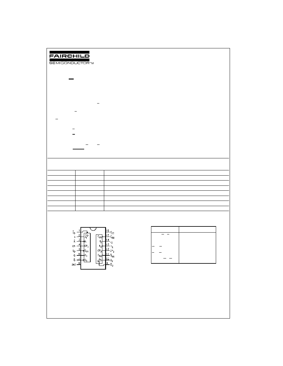
Connection Diagram
Pin Descriptions
FACT
is a trademark of Fairchild Semiconductor Corporation.
Order Number
Package Number
Package Description
74AC109SC
M16A
16-Lead Small Outline Integrated Circuit (SOIC), JEDEC MS-012, 0.150 Narrow
74AC109SJ
M16D
16-Lead Small Outline Package (SOP), EIAJ TYPE II, 5.3mm Wide
74AC109MTC
MTC16
16-Lead Thin Shrink Small Outline Package (TSSOP), JEDEC MO-153, 4.4mm Wide
74AC109PC
N16E
16-Lead Plastic Dual-in-Line Package (PDIP), JEDEC MS-001, 0.300" Wide
74ACT109SC
M16A
16-Lead Small Outline Integrated Circuit (SOIC), JEDEC MS-012, 0.150 Narrow
74AC109MTC
MTC16
16-Lead Thin Shrink Small Outline Package (TSSOP), JEDEC MO-153, 4.4mm Wide
74ACT109PC
N16E
16-Lead Plastic Dual-In-Line Package (PDIP), JEDEC MS-001, 0.300 Wide
Pin Names
Description
J
1
, J
2
, K
1
, K
2
Data Inputs
CP
1
, CP
2
Clock Pulse Inputs
C
D1
, C
D2
Direct Clear Inputs
S
D1
, S
D2
Direct Set Inputs
Q
1
, Q
2
, Q
1
, Q
2
Outputs
www.fairchildsemi.com
2
74AC109
∑
74ACT109
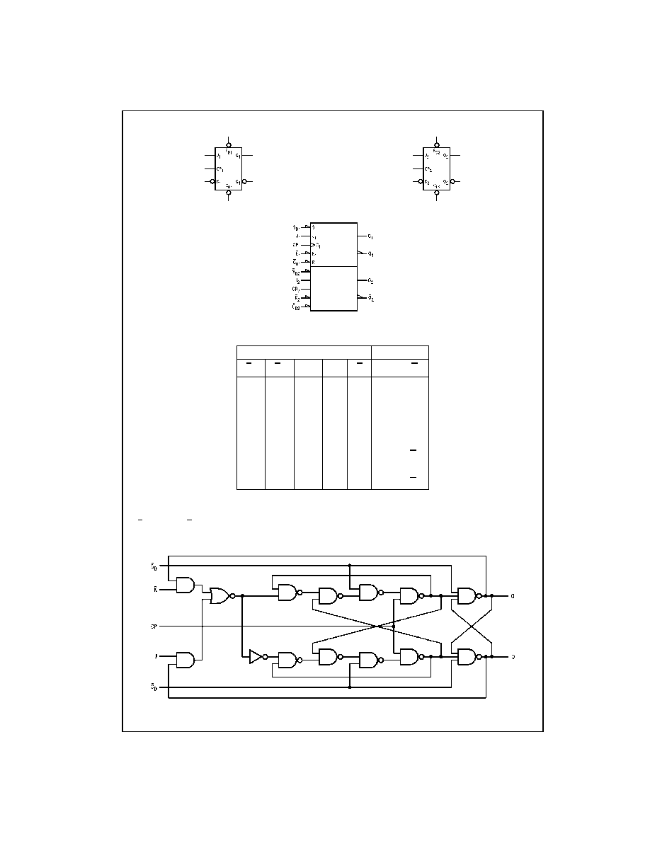
Logic Symbols
IEEE/IEC
Truth Table
(each half)
H
=
HIGH Voltage Level
L
=
LOW Voltage Level
=
LOW-to-HIGH Transition
X
=
Immaterial
Q
0
(Q
0
)
=
Previous Q
0
(Q
0
) before LOW-to-HIGH Transition of Clock
Logic Diagram
(one half shown)
Please note that this diagram is provided only for the understanding of logic operations and should not be used to estimate propagation delays.
Inputs
Outputs
S
D
C
D
CP
J
K
Q
Q
L
H
X
X
X
H
L
H
L
X
X
X
L
H
L
L
X
X
X
H
H
H
H
L
L
L
H
H
H
H
L
Toggle
H
H
L
H
Q
0
Q
0
H
H
H
H
H
L
H
H
L
X
X
Q
0
Q
0
3
www.fairchildsemi.com
74
A
C
10
9
∑
74ACT109
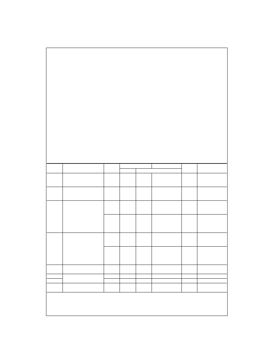
Absolute Maximum Ratings
(Note 1)
Recommended Operating
Conditions
Note 1: Absolute maximum ratings are those values beyond which damage
to the device may occur. The databook specifications should be met, with-
out exception, to ensure that the system design is reliable over its power
supply, temperature, and output/input loading variables.Fairchild does not
recommend operation of FACT
circuits outside databook specifications.
DC Electrical Characteristics for AC
Note 2: All outputs loaded; thresholds on input associated with output under test.
Note 3: Maximum test duration 2.0 ms, one output loaded at a time.
Note 4: I
IN
and I
CC
@ 3.0V are guaranteed to be less than or equal to the respective limit @ 5.5V V
CC
.
Supply Voltage (V
CC
)
-
0.5V to
+
7.0V
DC Input Diode Current (I
IK
)
V
I
=
-
0.5V
-
20 mA
V
I
=
V
CC
+
0.5V
+
20 mA
DC Input Voltage (V
I
)
-
0.5V to V
CC
+
0.5V
DC Output Diode Current (I
OK
)
V
O
=
-
0.5V
-
20 mA
V
O
=
V
CC
+
0.5V
+
20 mA
DC Output Voltage (V
O
)
-
0.5V to V
CC
+
0.5V
DC Output Source
or Sink Current (I
O
)
±
50 mA
DC V
CC
or Ground Current
per Output Pin (I
CC
or I
GND
)
±
50 mA
Storage Temperature (T
STG
)
-
65
∞
C to
+
150
∞
C
Junction Temperature (T
J
)
PDIP
140
∞
C
Supply Voltage (V
CC
)
AC
2.0V to 6.0V
ACT
4.5V to 5.5V
Input Voltage (V
I
)
0V to V
CC
Output Voltage (V
O
)
0V to V
CC
Operating Temperature (T
A
)
-
40
∞
C to
+
85
∞
C
Minimum Input Edge Rate (
V/
t)
AC Devices
V
IN
from 30% to 70% of V
CC
V
CC
@ 3.3V, 4.5V, 5.5V
125 mV/ns
Minimum Input Edge Rate (
V/
t)
ACT Devices
V
IN
from 0.8V to 2.0V
V
CC
@ 4.5V, 5.5V
125 mV/ns
Symbol
Parameter
V
CC
T
A
=
+
25
∞
C
T
A
=
-
40
∞
C to
+
85
∞
C
Units
Conditions
(V)
Typ
Guaranteed Limits
V
IH
Minimum HIGH Level
3.0
1.5
2.1
2.1
V
OUT
=
0.1V
Input Voltage
4.5
2.25
3.15
3.15
V
or V
CC
-
0.1V
5.5
2.75
3.85
3.85
V
IL
Maximum LOW Level
3.0
1.5
0.9
0.9
V
OUT
=
0.1V
Input Voltage
4.5
2.25
1.35
1.35
V
or V
CC
-
0.1V
5.5
2.75
1.65
1.65
V
OH
Minimum HIGH Level
3.0
2.99
2.9
2.9
Output Voltage
4.5
4.49
4.4
4.4
V
I
OUT
=
-
50
µ
A
5.5
5.49
5.4
5.4
V
IN
=
V
IL
or V
IH
3.0
2.56
2.46
I
OH
=
-
12 mA
4.5
3.86
3.76
V
I
OH
=
-
24 mA
5.5
4.86
4.76
I
OH
=
-
24 mA (Note 2)
V
OL
Maximum LOW Level
3.0
0.002
0.1
0.1
Output Voltage
4.5
0.001
0.1
0.1
V
I
OUT
=
50
µ
A
5.5
0.001
0.1
0.1
V
IN
=
V
IL
or V
IH
3.0
0.36
0.44
I
OL
=
12 mA
4.5
0.36
0.44
V
I
OL
=
24 mA
5.5
0.36
0.44
I
OL
=
24 mA (Note 2)
I
IN
Maximum Input
5.5
±
0.1
±
1.0
µ
A
V
I
=
V
CC,
(Note 4)
Leakage Current
GND
I
OLD
Minimum Dynamic
5.5
75
mA
V
OLD
=
1.65V Max
I
OHD
Output Current (Note 3)
5.5
-
75
mA
V
OHD
=
3.85V Min
I
CC
Maximum Quiescent
5.5
2.0
20.0
µ
A
V
IN
=
V
CC
(Note 4)
Supply Current
or GND
www.fairchildsemi.com
4
74AC109
∑
74ACT109
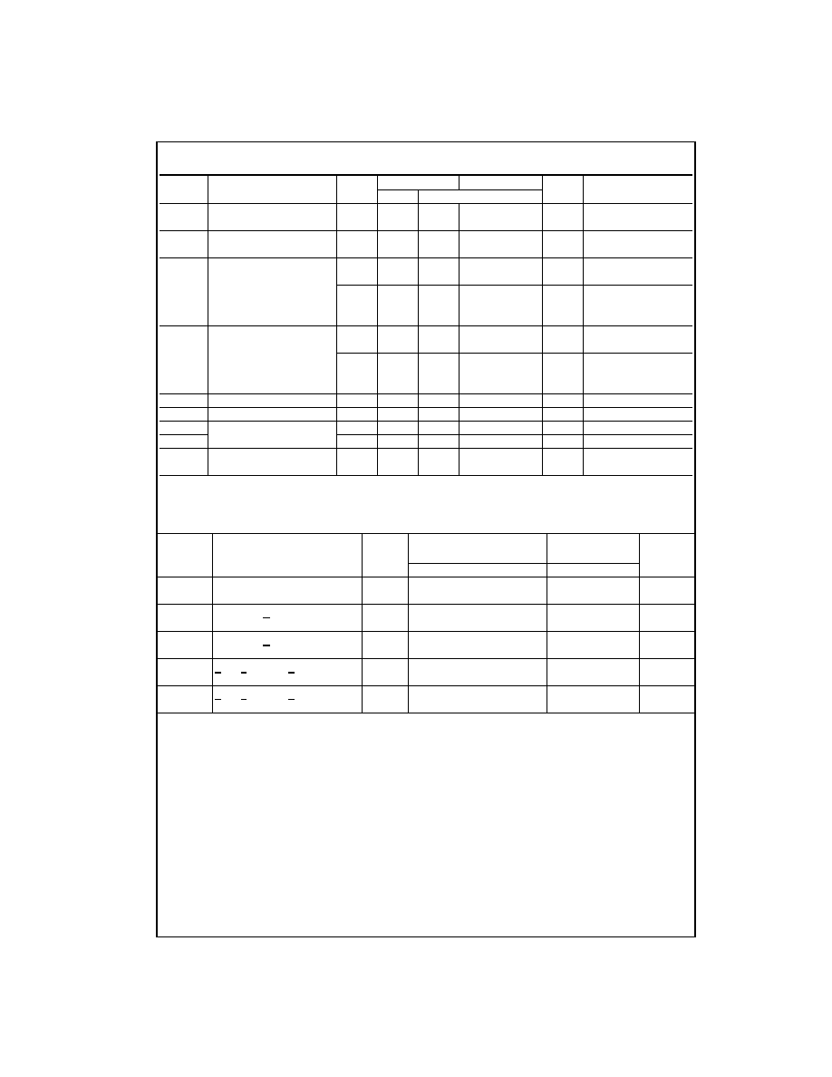
DC Electrical Characteristics for ACT
Note 5: All outputs loaded; thresholds on input associated with output under test.
Note 6: Maximum test duration 2.0 ms, one output loaded at a time.
AC Electrical Characteristics for AC
Note 7: Voltage Range 3.3 is 3.3V
±
0.3V
Voltage Range 5.0 is 5.0V
±
0.5V
Symbol
Parameter
V
CC
T
A
=
+
25
∞
C
T
A
=
-
40
∞
C to
+
85
∞
C
Units
Conditions
(V)
Typ
Guaranteed Limits
V
IH
Minimum HIGH Level
4.5
1.5
2.0
2.0
V
V
OUT
=
0.1V
Input Voltage
5.5
1.5
2.0
2.0
or V
CC
-
0.1V
V
IL
Maximum LOW Level
4.5
1.5
0.8
0.8
V
V
OUT
=
0.1V
Input Voltage
5.5
1.5
0.8
0.8
or V
CC
-
0.1V
V
OH
Minimum HIGH Level
4.5
4.49
4.4
4.4
V
I
OUT
=
-
50
µ
A
Output Voltage
5.5
5.49
5.4
5.4
V
IN
=
V
IL
or V
IH
4.5
3.86
3.76
V
I
OH
=
-
24 mA
5.5
4.86
4.76
I
OH
=
-
24 mA (Note 5)
V
OL
Maximum LOW Level
4.5
0.001
0.1
0.1
V
I
OUT
=
50
µ
A
Output Voltage
5.5
0.001
0.1
0.1
V
IN
=
V
IL
or V
IH
4.5
0.36
0.44
V
I
OL
=
24 mA
5.5
0.36
0.44
I
OL
=
24 mA (Note 5)
I
IN
Maximum Input Leakage Current
5.5
±
0.1
±
1.0
µ
A
FV
I
=
V
CC
, GND
I
CCT
Maximum I
CC
/Input
5.5
0.6
1.5
mA
V
I
=
V
CC
-
2.1V
I
OLD
Minimum Dynamic
5.5
75
mA
V
OLD
=
1.65V Max
I
OHD
Output Current (Note 6)
5.5
-
75
mA
V
OHD
=
3.85V Min
I
CC
Maximum Quiescent
5.5
2.0
20.0
µ
A
V
IN
=
V
CC
or GND
Supply Current
V
CC
T
A
=
+
25
∞
C
T
A
=
-
40
∞
C to
+
85
∞
C
Symbol
Parameter
(V)
C
L
=
50 pF
C
L
=
50 pF
Units
(Note 7)
Min
Typ
Max
Min
Max
f
MAX
Maximum Clock
3.3
125
150
100
MHz
Frequency
5.0
150
175
125
t
PLH
Propagation Delay
3.3
4.0
8.0
13.5
3.5
16.0
ns
CP
n
to Q
n
or Q
n
5.0
2.5
6.0
10.0
2.0
10.5
t
PHL
Propagation Delay
3.3
3.0
8.0
14.0
3.0
14.5
ns
CP
n
to Q
n
or Q
n
5.0
2.0
6.0
10.0
1.5
10.5
t
PLH
Propagation Delay
3.3
3.0
8.0
12.0
2.5
13.0
ns
C
Dn
or S
Dn
to Q
n
or Q
n
5.0
2.5
6.0
9.0
2.0
10.0
t
PHL
Propagation Delay
3.3
3.0
10.0
12.0
3.0
13.5
ns
C
Dn
or S
Dn
to Q
n
or Q
n
5.0
2.0
7.5
9.5
2.0
10.5
5
www.fairchildsemi.com
74
A
C
10
9
∑
74ACT109
AC Operating Requirements for AC
Note 8: Voltage Range 3.3 is 3.3V
±
0.3V
Voltage Range 5.0 is 5.0V
±
0.5V
AC Electrical Characteristics for ACT
Note 9: Voltage Range 5.0 is 5.0V
±
0.5V
AC Operating Requirements for ACT
Note 10: Voltage Range 5.0 is 5.0V
±
0.5V
Capacitance
V
CC
T
A
=
+
25
∞
C
T
A
=
-
40
∞
C to
+
85
∞
C
Symbol
Parameter
(V)
C
L
=
50 pF
C
L
=
50 pF
Units
(Note 8)
Typ
Guaranteed Minimum
t
S
Setup Time, HIGH or LOW
3.3
3.5
6.5
7.5
ns
J
n
or K
n
to CP
n
5.0
2.0
4.5
5.0
t
H
Hold Time, HIGH or LOW
3.3
-
1.5
0
0
ns
J
n
or K
n
to CP
n
5.0
-
0.5
0.5
0.5
t
W
Pulse Width
3.3
2.0
7.0
7.5
ns
C
Dn
or S
Dn
5.0
2.0
4.5
5.0
t
REC
Recovery Time
3.3
-
2.5
0
0
ns
C
Dn
or S
Dn
to CP
n
5.0
-
1.5
0
0
V
CC
T
A
=
+
25
∞
C
T
A
=
-
40
∞
C to
+
85
∞
C
Symbol
Parameter
(V)
C
L
=
50 pF
C
L
=
50 pF
Units
(Note 9)
Min
Typ
Max
Min
Max
f
MAX
Maximum Clock Frequency
5.0
145
210
125
MHz
t
PLH
Propagation Delay
5.0
4.0
7.0
11.0
3.5
13.0
ns
CP
n
to Q
n
or Q
n
t
PHL
Propagation Delay
5.0
3.0
6.0
10.0
2.5
11.5
ns
CP
n
to Q
n
or Q
n
t
PLH
Propagation Delay
5.0
2.5
5.5
9.5
2.0
10.5
ns
C
Dn
or S
Dn
to Q
n
or Q
n
t
PHL
Propagation Delay
5.0
2.5
6.0
10.0
2.0
11.5
ns
C
Dn
or S
Dn
to Q
n
or Q
n
V
CC
T
A
=
+
25
∞
C
T
A
=
-
40
∞
C to
+
85
∞
C
Symbol
Parameter
(V)
C
L
=
50 pF
C
L
=
50 pF
Units
(Note 10)
Typ
Guaranteed Minimum
t
S
Setup Time, HIGH or LOW
5.0
0.5
2.0
2.5
ns
J
n
or K
n
to CP
n
t
H
Hold Time, HIGH or LOW
5.0
0
2.0
2.0
ns
J
n
or K
n
to CP
n
t
W
Pulse Width
5.0
3.0
5.0
6.0
ns
CP
n
or C
Dn
or S
Dn
t
rec
Recovery Time
5.0
-
2.5
0
0
ns
C
Dn
or S
Dn
to CP
n
Symbol
Parameter
Typ
Units
Conditions
C
IN
Input Capacitance
4.5
pF
V
CC
=
OPEN
C
PD
Power Dissipation Capacitance
35.0
pF
V
CC
=
5.0V
www.fairchildsemi.com
6
74AC109
∑
74ACT109
Physical Dimensions
inches (millimeters) unless otherwise noted
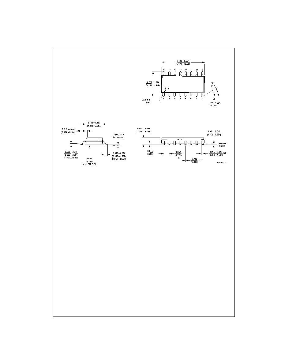
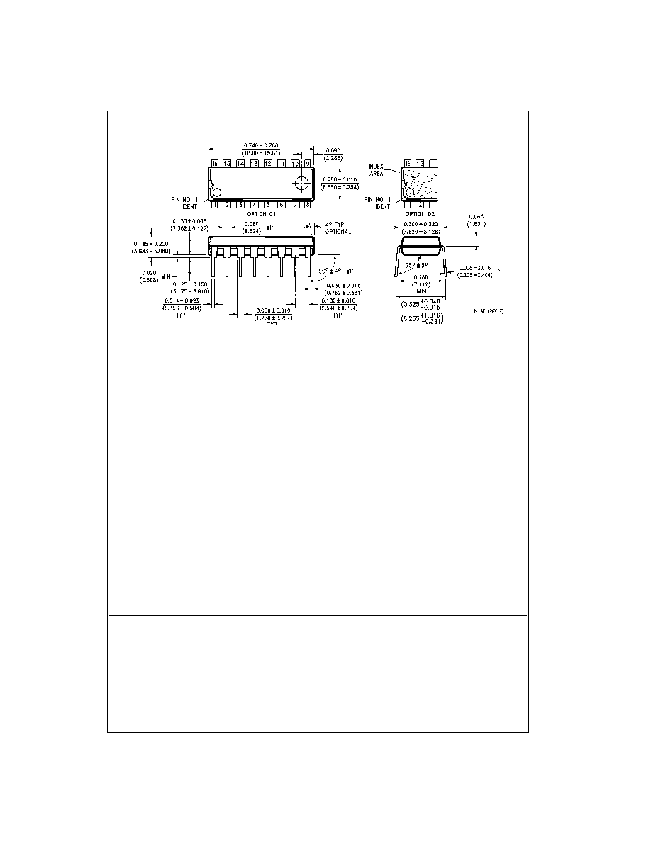
16-Lead Small Outline Integrated Circuit (SOIC), JEDEC MS-012, 0.150 Narrow
Package Number M16A

7
www.fairchildsemi.com
74
A
C
10
9
∑
74ACT109
Physical Dimensions
inches (millimeters) unless otherwise noted (Continued)
16-Lead Small Outline Package (SOP), EIAJ TYPE II, 5.3mm Wide
Package Number M16D
www.fairchildsemi.com
8
74AC109
∑
74ACT109
Physical Dimensions
inches (millimeters) unless otherwise noted (Continued)
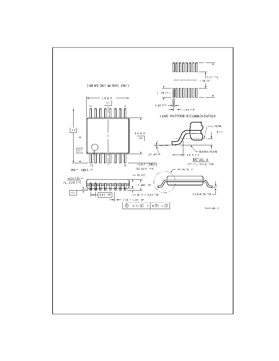
16-Lead Thin Shrink Small Outline Package (TSSOP), JEDEC MO-153, 4.4mm Wide
Package Number MTC16
9
www.fairchildsemi.com
74
A
C
10
9
∑
74ACT109 Dual JK
Posi
ti
ve Edge-T
r
i
gg
ered Fli
p
-Fl
o
p
Physical Dimensions
inches (millimeters) unless otherwise noted (Continued)
16-Lead Plastic Dual-In-Line Package (PDIP), JEDEC MS-001, 0.300 Wide
Package Number N16E
Fairchild does not assume any responsibility for use of any circuitry described, no circuit patent licenses are implied and
Fairchild reserves the right at any time without notice to change said circuitry and specifications.
LIFE SUPPORT POLICY
FAIRCHILD'S PRODUCTS ARE NOT AUTHORIZED FOR USE AS CRITICAL COMPONENTS IN LIFE SUPPORT
DEVICES OR SYSTEMS WITHOUT THE EXPRESS WRITTEN APPROVAL OF THE PRESIDENT OF FAIRCHILD
SEMICONDUCTOR CORPORATION. As used herein:
1. Life support devices or systems are devices or systems
which, (a) are intended for surgical implant into the
body, or (b) support or sustain life, and (c) whose failure
to perform when properly used in accordance with
instructions for use provided in the labeling, can be rea-
sonably expected to result in a significant injury to the
user.
2. A critical component in any component of a life support
device or system whose failure to perform can be rea-
sonably expected to cause the failure of the life support
device or system, or to affect its safety or effectiveness.
www.fairchildsemi.com